WO2024176757A1 - 保護膜形成用組成物、半導体基板、及び電子部品 - Google Patents
保護膜形成用組成物、半導体基板、及び電子部品 Download PDFInfo
- Publication number
- WO2024176757A1 WO2024176757A1 PCT/JP2024/003036 JP2024003036W WO2024176757A1 WO 2024176757 A1 WO2024176757 A1 WO 2024176757A1 JP 2024003036 W JP2024003036 W JP 2024003036W WO 2024176757 A1 WO2024176757 A1 WO 2024176757A1
- Authority
- WO
- WIPO (PCT)
- Prior art keywords
- protective film
- semiconductor substrate
- foreign matter
- forming
- composition
- Prior art date
- Legal status (The legal status is an assumption and is not a legal conclusion. Google has not performed a legal analysis and makes no representation as to the accuracy of the status listed.)
- Ceased
Links
Images







Classifications
-
- C—CHEMISTRY; METALLURGY
- C09—DYES; PAINTS; POLISHES; NATURAL RESINS; ADHESIVES; COMPOSITIONS NOT OTHERWISE PROVIDED FOR; APPLICATIONS OF MATERIALS NOT OTHERWISE PROVIDED FOR
- C09J—ADHESIVES; NON-MECHANICAL ASPECTS OF ADHESIVE PROCESSES IN GENERAL; ADHESIVE PROCESSES NOT PROVIDED FOR ELSEWHERE; USE OF MATERIALS AS ADHESIVES
- C09J5/00—Adhesive processes in general; Adhesive processes not provided for elsewhere, e.g. relating to primers
- C09J5/02—Adhesive processes in general; Adhesive processes not provided for elsewhere, e.g. relating to primers involving pretreatment of the surfaces to be joined
-
- C—CHEMISTRY; METALLURGY
- C08—ORGANIC MACROMOLECULAR COMPOUNDS; THEIR PREPARATION OR CHEMICAL WORKING-UP; COMPOSITIONS BASED THEREON
- C08K—Use of inorganic or non-macromolecular organic substances as compounding ingredients
- C08K5/00—Use of organic ingredients
- C08K5/04—Oxygen-containing compounds
- C08K5/06—Ethers; Acetals; Ketals; Ortho-esters
-
- C—CHEMISTRY; METALLURGY
- C08—ORGANIC MACROMOLECULAR COMPOUNDS; THEIR PREPARATION OR CHEMICAL WORKING-UP; COMPOSITIONS BASED THEREON
- C08L—COMPOSITIONS OF MACROMOLECULAR COMPOUNDS
- C08L101/00—Compositions of unspecified macromolecular compounds
- C08L101/02—Compositions of unspecified macromolecular compounds characterised by the presence of specified groups, e.g. terminal or pendant functional groups
- C08L101/06—Compositions of unspecified macromolecular compounds characterised by the presence of specified groups, e.g. terminal or pendant functional groups containing oxygen atoms
-
- C—CHEMISTRY; METALLURGY
- C09—DYES; PAINTS; POLISHES; NATURAL RESINS; ADHESIVES; COMPOSITIONS NOT OTHERWISE PROVIDED FOR; APPLICATIONS OF MATERIALS NOT OTHERWISE PROVIDED FOR
- C09D—COATING COMPOSITIONS, e.g. PAINTS, VARNISHES OR LACQUERS; FILLING PASTES; CHEMICAL PAINT OR INK REMOVERS; INKS; CORRECTING FLUIDS; WOODSTAINS; PASTES OR SOLIDS FOR COLOURING OR PRINTING; USE OF MATERIALS THEREFOR
- C09D125/00—Coating compositions based on homopolymers or copolymers of compounds having one or more unsaturated aliphatic radicals, each having only one carbon-to-carbon double bond, and at least one being terminated by an aromatic carbocyclic ring; Coating compositions based on derivatives of such polymers
- C09D125/02—Homopolymers or copolymers of hydrocarbons
- C09D125/04—Homopolymers or copolymers of styrene
- C09D125/06—Polystyrene
-
- C—CHEMISTRY; METALLURGY
- C09—DYES; PAINTS; POLISHES; NATURAL RESINS; ADHESIVES; COMPOSITIONS NOT OTHERWISE PROVIDED FOR; APPLICATIONS OF MATERIALS NOT OTHERWISE PROVIDED FOR
- C09D—COATING COMPOSITIONS, e.g. PAINTS, VARNISHES OR LACQUERS; FILLING PASTES; CHEMICAL PAINT OR INK REMOVERS; INKS; CORRECTING FLUIDS; WOODSTAINS; PASTES OR SOLIDS FOR COLOURING OR PRINTING; USE OF MATERIALS THEREFOR
- C09D5/00—Coating compositions, e.g. paints, varnishes or lacquers, characterised by their physical nature or the effects produced; Filling pastes
- C09D5/008—Temporary coatings
-
- G—PHYSICS
- G03—PHOTOGRAPHY; CINEMATOGRAPHY; ANALOGOUS TECHNIQUES USING WAVES OTHER THAN OPTICAL WAVES; ELECTROGRAPHY; HOLOGRAPHY
- G03F—PHOTOMECHANICAL PRODUCTION OF TEXTURED OR PATTERNED SURFACES, e.g. FOR PRINTING, FOR PROCESSING OF SEMICONDUCTOR DEVICES; MATERIALS THEREFOR; ORIGINALS THEREFOR; APPARATUS SPECIALLY ADAPTED THEREFOR
- G03F7/00—Photomechanical, e.g. photolithographic, production of textured or patterned surfaces, e.g. printing surfaces; Materials therefor, e.g. comprising photoresists; Apparatus specially adapted therefor
- G03F7/004—Photosensitive materials
- G03F7/039—Macromolecular compounds which are photodegradable, e.g. positive electron resists
-
- H—ELECTRICITY
- H10—SEMICONDUCTOR DEVICES; ELECTRIC SOLID-STATE DEVICES NOT OTHERWISE PROVIDED FOR
- H10P—GENERIC PROCESSES OR APPARATUS FOR THE MANUFACTURE OR TREATMENT OF DEVICES COVERED BY CLASS H10
- H10P52/00—Grinding, lapping or polishing of wafers, substrates or parts of devices
-
- H—ELECTRICITY
- H10—SEMICONDUCTOR DEVICES; ELECTRIC SOLID-STATE DEVICES NOT OTHERWISE PROVIDED FOR
- H10P—GENERIC PROCESSES OR APPARATUS FOR THE MANUFACTURE OR TREATMENT OF DEVICES COVERED BY CLASS H10
- H10P72/00—Handling or holding of wafers, substrates or devices during manufacture or treatment thereof
- H10P72/70—Handling or holding of wafers, substrates or devices during manufacture or treatment thereof for supporting or gripping
- H10P72/74—Handling or holding of wafers, substrates or devices during manufacture or treatment thereof for supporting or gripping using temporarily an auxiliary support
-
- H—ELECTRICITY
- H10—SEMICONDUCTOR DEVICES; ELECTRIC SOLID-STATE DEVICES NOT OTHERWISE PROVIDED FOR
- H10P—GENERIC PROCESSES OR APPARATUS FOR THE MANUFACTURE OR TREATMENT OF DEVICES COVERED BY CLASS H10
- H10P72/00—Handling or holding of wafers, substrates or devices during manufacture or treatment thereof
- H10P72/70—Handling or holding of wafers, substrates or devices during manufacture or treatment thereof for supporting or gripping
- H10P72/74—Handling or holding of wafers, substrates or devices during manufacture or treatment thereof for supporting or gripping using temporarily an auxiliary support
- H10P72/7412—Handling or holding of wafers, substrates or devices during manufacture or treatment thereof for supporting or gripping using temporarily an auxiliary support the auxiliary support including means facilitating the separation of a device or wafer from the auxiliary support
-
- H—ELECTRICITY
- H10—SEMICONDUCTOR DEVICES; ELECTRIC SOLID-STATE DEVICES NOT OTHERWISE PROVIDED FOR
- H10P—GENERIC PROCESSES OR APPARATUS FOR THE MANUFACTURE OR TREATMENT OF DEVICES COVERED BY CLASS H10
- H10P72/00—Handling or holding of wafers, substrates or devices during manufacture or treatment thereof
- H10P72/70—Handling or holding of wafers, substrates or devices during manufacture or treatment thereof for supporting or gripping
- H10P72/74—Handling or holding of wafers, substrates or devices during manufacture or treatment thereof for supporting or gripping using temporarily an auxiliary support
- H10P72/7416—Handling or holding of wafers, substrates or devices during manufacture or treatment thereof for supporting or gripping using temporarily an auxiliary support used during dicing or grinding
-
- H—ELECTRICITY
- H10—SEMICONDUCTOR DEVICES; ELECTRIC SOLID-STATE DEVICES NOT OTHERWISE PROVIDED FOR
- H10P—GENERIC PROCESSES OR APPARATUS FOR THE MANUFACTURE OR TREATMENT OF DEVICES COVERED BY CLASS H10
- H10P95/00—Generic processes or apparatus for manufacture or treatments not covered by the other groups of this subclass
-
- H—ELECTRICITY
- H10—SEMICONDUCTOR DEVICES; ELECTRIC SOLID-STATE DEVICES NOT OTHERWISE PROVIDED FOR
- H10W—GENERIC PACKAGES, INTERCONNECTIONS, CONNECTORS OR OTHER CONSTRUCTIONAL DETAILS OF DEVICES COVERED BY CLASS H10
- H10W72/00—Interconnections or connectors in packages
- H10W72/01—Manufacture or treatment
- H10W72/013—Manufacture or treatment of die-attach connectors
-
- H—ELECTRICITY
- H10—SEMICONDUCTOR DEVICES; ELECTRIC SOLID-STATE DEVICES NOT OTHERWISE PROVIDED FOR
- H10W—GENERIC PACKAGES, INTERCONNECTIONS, CONNECTORS OR OTHER CONSTRUCTIONAL DETAILS OF DEVICES COVERED BY CLASS H10
- H10W72/00—Interconnections or connectors in packages
- H10W72/01—Manufacture or treatment
- H10W72/013—Manufacture or treatment of die-attach connectors
- H10W72/01371—Cleaning, e.g. oxide removal or de-smearing
-
- C—CHEMISTRY; METALLURGY
- C09—DYES; PAINTS; POLISHES; NATURAL RESINS; ADHESIVES; COMPOSITIONS NOT OTHERWISE PROVIDED FOR; APPLICATIONS OF MATERIALS NOT OTHERWISE PROVIDED FOR
- C09J—ADHESIVES; NON-MECHANICAL ASPECTS OF ADHESIVE PROCESSES IN GENERAL; ADHESIVE PROCESSES NOT PROVIDED FOR ELSEWHERE; USE OF MATERIALS AS ADHESIVES
- C09J2203/00—Applications of adhesives in processes or use of adhesives in the form of films or foils
- C09J2203/326—Applications of adhesives in processes or use of adhesives in the form of films or foils for bonding electronic components such as wafers, chips or semiconductors
-
- C—CHEMISTRY; METALLURGY
- C09—DYES; PAINTS; POLISHES; NATURAL RESINS; ADHESIVES; COMPOSITIONS NOT OTHERWISE PROVIDED FOR; APPLICATIONS OF MATERIALS NOT OTHERWISE PROVIDED FOR
- C09J—ADHESIVES; NON-MECHANICAL ASPECTS OF ADHESIVE PROCESSES IN GENERAL; ADHESIVE PROCESSES NOT PROVIDED FOR ELSEWHERE; USE OF MATERIALS AS ADHESIVES
- C09J2301/00—Additional features of adhesives in the form of films or foils
- C09J2301/50—Additional features of adhesives in the form of films or foils characterized by process specific features
- C09J2301/502—Additional features of adhesives in the form of films or foils characterized by process specific features process for debonding adherents
-
- C—CHEMISTRY; METALLURGY
- C09—DYES; PAINTS; POLISHES; NATURAL RESINS; ADHESIVES; COMPOSITIONS NOT OTHERWISE PROVIDED FOR; APPLICATIONS OF MATERIALS NOT OTHERWISE PROVIDED FOR
- C09J—ADHESIVES; NON-MECHANICAL ASPECTS OF ADHESIVE PROCESSES IN GENERAL; ADHESIVE PROCESSES NOT PROVIDED FOR ELSEWHERE; USE OF MATERIALS AS ADHESIVES
- C09J2425/00—Presence of styrenic polymer
- C09J2425/003—Presence of styrenic polymer in the primer coating
Definitions
- the present invention relates to a composition for forming a protective film that can protect semiconductor substrates, electronic components, etc. from foreign matter, scratches, breakage, etc., and to a method for manufacturing semiconductor substrates, electronic components, and processed semiconductor substrates.
- a process is being considered in which a semiconductor substrate (e.g., a wafer) is attached to a support substrate, then back-grinding (grinding), wiring creation processes, etc. are carried out, and then the support substrate is peeled off to obtain the desired semiconductor substrate.
- a semiconductor substrate e.g., a wafer
- back-grinding grinding
- wiring creation processes etc.
- Patent Documents 1 and 2 disclose a composition for forming a substrate processing film and a substrate processing method that can efficiently remove minute particles from the substrate surface and easily remove the formed substrate processing film from the substrate surface in a process of forming a substrate processing film on the surface of a semiconductor substrate and removing foreign matter from the substrate surface.
- the semiconductor substrate when attaching a semiconductor substrate to a support substrate, the semiconductor substrate is attached using an adhesive layer (e.g., a liquid composition containing a polymer, a backgrind tape, a dicing tape, etc.) that is resistant to subsequent processes (e.g., a heating process, a chemical treatment process, etc.).
- an adhesive layer e.g., a liquid composition containing a polymer, a backgrind tape, a dicing tape, etc.
- a support substrate having an adhesive layer is used.
- a process of peeling off the semiconductor substrate is performed.
- the adhesive layer or the adhesive layer of the support substrate may remain on the substrate as a foreign matter (residue). This occurs particularly noticeably when an adhesive layer is formed directly on the surface of a semiconductor substrate on which wiring, etc. has already been formed, or when a support substrate having an adhesive layer is attached directly. This foreign matter may not be completely removed even if cleaning is performed with known organic solvents, liquid chemicals, etc.
- chip mounting When electronic components (also called semiconductor chips) are mounted on printed circuit boards, etc., a process called chip mounting is carried out.
- chip mounting an electronic component is picked up from a reel or tray on which multiple electronic components are placed using a gripping member such as a suction nozzle, and the electronic component is placed in the desired position on the printed circuit board.
- a gripping member such as a suction nozzle
- an object of the present invention is to provide a composition for forming a protective film that can protect semiconductor substrates, electronic components, etc. from foreign matter, scratches, breakage, etc. and can form a protective film that is easily removable.
- Another object of the present invention is to provide a protective film formed from the composition for forming a protective film, a semiconductor substrate or electronic component having the protective film, and a method for manufacturing a processed semiconductor substrate using the protective film.
- a composition for forming a protective film comprising: a polymer (A) having at least one of a phenolic hydroxy group and a carboxy group; a vinyl ether group-containing crosslinking agent (B); a photoacid generator (C); and a solvent (D).
- R 3 each independently represents a divalent organic group; and n1 represents an integer of 2 to 6.
- a method for producing a processed semiconductor substrate comprising the steps of: A first step of manufacturing a laminate by bonding the semiconductor substrate according to [9] and a supporting base material via the coating film for removing foreign matter, which is the protective film; A second step of processing the laminate; A third step of irradiating the coating film for removing foreign matter with light; A fourth step of peeling off the supporting substrate from the laminate; and a fifth step of washing the semiconductor substrate or the supporting substrate with a remover to remove the foreign matter removing coating film.
- the method for producing a processed semiconductor substrate according to [11] wherein in the fifth step, foreign matter is removed together with the foreign matter removal coating film.
- the present invention can provide a composition for forming a protective film that can protect semiconductor substrates, electronic components, and the like from foreign matter, scratches, breakage, and the like, and can form a protective film that is easily removable.
- the present invention can also provide a protective film formed from the composition for forming a protective film, a semiconductor substrate or electronic component having the protective film, and a method for producing a processed semiconductor substrate using the protective film.
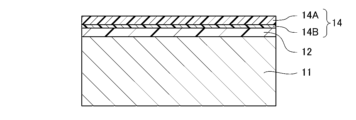
- FIG. 1A is a schematic cross-sectional view for explaining an example of a method for manufacturing a processed semiconductor substrate (part 1).
- FIG. 1B is a schematic cross-sectional view for explaining one example of a method for manufacturing a processed semiconductor substrate (part 2).
- FIG. 1C is a schematic cross-sectional view for explaining one example of a method for manufacturing a processed semiconductor substrate (part 3).
- FIG. 1D is a schematic cross-sectional view for explaining one example of a method for manufacturing a processed semiconductor substrate (part 4).
- FIG. 1E is a schematic cross-sectional view for explaining an example of a method for manufacturing a processed semiconductor substrate (part 5).
- FIG. 1F is a schematic cross-sectional view for explaining one example of a method for manufacturing a processed semiconductor substrate (part 6).
- FIG. 1G is a schematic cross-sectional view for explaining one example of a method for manufacturing a processed semiconductor substrate (part 7).
- FIG. 1H is a schematic cross-sectional view for explaining one example of a method for manufacturing a processed semiconductor substrate (part 8).
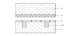
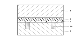
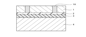
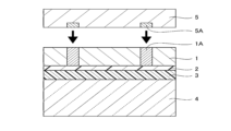
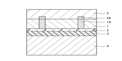
- FIG. 2A is a schematic cross-sectional view (part 1) for explaining another example of a method for manufacturing a processed semiconductor substrate.
- FIG. 2B is a schematic cross-sectional view (part 2) for explaining another example of a method for manufacturing a processed semiconductor substrate.
- FIG. 2C is a schematic cross-sectional view (part 3) for explaining another example of the method for manufacturing a processed semiconductor substrate.
- FIG. 1G is a schematic cross-sectional view for explaining one example of a method for manufacturing a processed semiconductor substrate (part 7).
- FIG. 1H is a schematic cross-sectional view for explaining one example of a method for manufacturing a processed semiconductor substrate (part 8).
- FIG. 2A is a schematic cross-sectional view (part 1)
- FIG. 2D is a schematic cross-sectional view (part 4) for explaining another example of a method for manufacturing a processed semiconductor substrate.
- FIG. 2E is a schematic cross-sectional view (part 5) for explaining another example of a method for manufacturing a processed semiconductor substrate.
- FIG. 2F is a schematic cross-sectional view (part 6) for explaining another example of a method for manufacturing a processed semiconductor substrate.
- FIG. 2G is a schematic cross-sectional view (part 7) for explaining another example of a method for manufacturing a processed semiconductor substrate.
- FIG. 2H is a schematic cross-sectional view (part 8) for explaining another example of a method for manufacturing a processed semiconductor substrate.
- FIG. 2I is a schematic cross-sectional view (part 9) for explaining another example of a method for manufacturing a processed semiconductor substrate.
- FIG. 2J is a schematic cross-sectional view (part 10) for explaining another example of a method for manufacturing a processed semiconductor substrate.
- FIG. 2K is a schematic cross-sectional view (part 11) for explaining another example of a method for manufacturing a processed semiconductor substrate.
- FIG. 2L is a schematic cross-sectional view (part 12) for explaining another example of a method for manufacturing a processed semiconductor substrate.
- the composition for forming a protective film of the present invention contains a polymer (A), a crosslinking agent (B), a photoacid generator (C) and a solvent (D).
- the polymer (A) has at least one of a phenolic hydroxy group and a carboxy group.
- the crosslinking agent (B) has at least two vinyl ether groups.
- the crosslinking agent (B) may be referred to as a vinyl ether group-containing crosslinking agent (B).
- the composition for forming a protective film may contain an acetalization catalyst (E) as another component.
- an acetal structure is formed by a reaction (acetalization reaction) between a phenolic hydroxy group or a carboxy group in the polymer (A) and a vinyl ether group in the vinyl ether group-containing crosslinking agent (B) by heating or the like.
- a protective film having a crosslinked structure has solvent resistance (e.g., resistance to organic solvents and alkaline removal solutions).
- solvent resistance e.g., resistance to organic solvents and alkaline removal solutions.
- the crosslinked structure is decomposed by the decomposition of the acetal structure by the acid generated from the photoacid generator.
- a solvent e.g., an organic solvent or an alkaline removal solution
- the light may be laser light or non-laser light.
- the wavelength of the light is not particularly limited, and may be, for example, 210 nm to 440 nm.
- Examples of light sources include low-pressure mercury lamps (germicidal lamps, fluorescent chemical lamps, black lights), high-pressure discharge lamps (high-pressure mercury lamps, metal halide lamps), short arc discharge lamps (ultra-high-pressure mercury lamps, xenon lamps, mercury-xenon lamps), and light-emitting diodes (LEDs).
- the amount of irradiation is not particularly limited, and may be, for example, 5 mJ/cm 2 to 1,000 mJ/cm 2 .
- the protective film-forming composition is preferably a composition for forming a coating film for removing foreign matter, which is a protective film that protects a semiconductor substrate from foreign matter.
- the composition for forming a protective film is preferably a composition for forming a protective film for preventing scratches or damage to electronic components.
- the protective film-forming composition of the present invention is not a composition for forming an antireflective film.
- the antireflective film-forming composition is a composition for forming an antireflective film used in a lithography process for manufacturing a semiconductor device.
- the antireflective film-forming composition is a composition for forming an antireflective film provided between a photoresist and a substrate.
- the composition for forming a protective film of the present invention is not the composition for forming an anti-reflective film described in WO2005/111724.
- the polymer (A) has at least one of a phenolic hydroxy group and a carboxy group.
- the sum of the numbers of phenolic hydroxy groups and carboxy groups contained in polymer (A) is, for example, 2 or more.
- the number of phenolic hydroxy groups may be 2 or more and no carboxy groups may be contained, or the number of carboxy groups may be 2 or more and no phenolic hydroxy groups may be contained.
- the polymer (A) is not particularly limited as long as it has at least one of a phenolic hydroxy group and a carboxy group, and examples of the polymer include phenol novolac, cresol novolac, polyhydroxystyrene, polyamic acid, and polyacrylic acid.
- the polymer (A) a polymer in which all of the units (repeating unit structures) constituting the polymer have a phenolic hydroxy group or a carboxyl group can be used.
- a polymer composed of a unit having a phenolic hydroxy group or a carboxyl group and a unit not having a phenolic hydroxy group or a carboxyl group can also be used.
- the molar ratio of the unit having a phenolic hydroxy group or a carboxyl group in the polymer is preferably 1% or more, for example 10% or more, and particularly 20% or more, based on the total units constituting the polymer.
- the molar ratio of the unit having a phenolic hydroxy group or a carboxyl group in the polymer is 5% to 100%, for example 10% to 100%, preferably 20% to 100%, and more preferably 30% to 100%. %.
- Examples of the polymer (A) include polymers represented by the following formulas (4) to (23) and (26) to (35), in which p1 , p2 , p3 and p4 each represent the molar proportion of each unit in the polymer, and the sum of these represents a value that is 100%.
- Polymer (A) includes polymers (e.g., polyhydroxystyrene) containing hydroxystyrene units (repeating units derived from hydroxystyrene).
- Polymer (A) also includes polymers produced by copolymerization of hydroxystyrene with compounds having addition polymerizable double bonds, such as acrylic acid ester compounds, methacrylic acid ester compounds, maleimides, and vinyl ether compounds, for example, polymers of formulas (8) to (11).
- the hydroxystyrene units are contained in a molar ratio of 10% or more with respect to all units constituting the polymer.
- the molar ratio of the hydroxystyrene units in the polymer is 10% or more, preferably 20% or more, with respect to all units constituting the polymer, for example, 10% to 100%, preferably 20% to 100%, more preferably 30% to 100%.
- Polymer (A) also includes polymers containing acrylic acid units or methacrylic acid units (e.g., polyacrylic acid or polymethacrylic acid polymers).
- Polymer (A) also includes polymers produced from compounds having addition polymerizable double bonds, such as acrylic acid ester compounds, methacrylic acid ester compounds, and styrene compounds, and acrylic acid or methacrylic acid, such as polymers of formulas (10), (12) to (15). From the viewpoint of the solubility of the protective film in an alkaline removal solution after irradiation with light, it is preferable that the acrylic acid units or methacrylic acid units are contained in a molar ratio of 10% or more with respect to the total units constituting the polymer.
- the molar ratio of the acrylic acid units or methacrylic acid units in the polymer is 10% or more, preferably 20% or more, with respect to the total units constituting the polymer, for example, 10% to 100%, preferably 20% to 90%, and more preferably 30% to 70%.
- Polymer (A) may also be a polyimide.
- the polyimide used in the present invention may be produced from a tetracarboxylic dianhydride compound and a diamine compound having a phenolic hydroxyl group or a carboxyl group.
- Examples of such polyimides include polyimides of formulas (31) to (35).
- the polyimide of formula (31) may be obtained by reacting a 1,2,4,5-benzenetetracarboxylic dianhydride compound with 3,5-diaminobenzoic acid and 2,2-bis(3-amino-4-toluyl)hexafluoropropane.
- Polymer (A) may also include polyamic acids.
- Polyamic acids may be produced by reacting a diamine compound with a tetracarboxylic acid or its derivatives, such as a tetracarboxylic dianhydride compound or a dicarboxylic dihalide.
- Polyamic acids may also be produced by synthesizing a polyamic acid silyl ester by polymerization using a bissilylated diamine compound and a tetracarboxylic dianhydride compound, and then decomposing the silyl ester portion with an acid.
- Examples of polyamic acids used in the present invention include polyamic acids of formulas (16) to (23) and (26) to (30).
- polyamic acid of formula (20) may be obtained by reacting a 1,2,4,5-benzenetetracarboxylic dianhydride compound with 3,5-diaminobenzoic acid and 2,2'-bis(trifluoromethyl)-4,4'-diaminobiphenyl.
- Polymer (A) also includes polymers made from a compound having at least two epoxy groups and a compound having at least two phenolic hydroxyl or carboxyl groups, such as those made from a compound having at least two, e.g., from two to six, epoxy groups and a compound having at least two, e.g., from two to six, phenolic hydroxyl or carboxyl groups.
- a polymer can be produced by reacting a compound having at least two epoxy groups with a compound having at least two phenolic hydroxyl groups or carboxyl groups in an amount approximately equimolar to the epoxy groups, in the presence of a catalyst such as a quaternary ammonium salt.
- Examples of compounds having at least two epoxy groups include tris(2,3-epoxypropyl)isocyanurate, 1,4-butanediol diglycidyl ether, 1,2-epoxy-4-(epoxyethyl)cyclohexane, glycerol triglycidyl ether, diethylene glycol diglycidyl ether, 2,6-diglycidylphenyl glycidyl ether, 1,1,3-tris[p-(2,3-epoxypropoxy)phenyl]propane, 1,2-cyclohexanedicarboxylic acid diglycidyl ester, 4,4'-methylenebis(N,N-diglycidylaniline), 3,4-epoxycyclohexylmethyl-3,4-epoxycyclohexanecarboxylate, trimethylolethane triglycidyl ether, bisphenol-A diglycidyl ether, and pentaerythrito
- Examples of the compound having at least two phenolic hydroxyl groups or carboxyl groups include 1,2,3-anthracene triol, 2,7,9-anthracene triol, 2-hydroxy-1-naphthoic acid, 7-hydroxy-1-naphthoic acid, 3-hydroxy-2-naphthoic acid, 2,6-naphthoic acid, 1-hydroxy-4-phenyl-3-naphthoic acid, 6-ethoxy-2,3-naphthalenediol, 4-hydroxybenzoic acid, 2-chloro-4-hydroxybenzoic acid, 2,4-dihydroxy-5-methylbenzoic acid,
- Examples of the hydroxybenzoic acid include 3-hydroxybenzoic acid, 5-hydroxyisophthalic acid, 2,5-dihydroxybenzoic acid, terephthalic acid, 2-nitroterephthalic acid, 3,5-dibromo-4-hydroxybenzoic acid, 3,5-dibromo-2,4-dihydroxybenzoic acid, 3-i
- the polymer (A) may also be represented by the formula (1): (In formula (1), R 1 represents a hydrogen atom or a methyl group. X represents -O- or -N(R 3 )-(R 3 represents a hydrogen atom or a methyl group). R 2 represents a single bond or an alkylene group having 1 to 6 carbon atoms. R 11 represents an alkyl group having 1 to 6 carbon atoms. m represents an integer of 0 to 4. When m is 2 or more, two or more R 11 may be the same or different.) can be used.
- the unit of formula (1) is contained in a molar ratio of, for example, 10% or more relative to all units constituting the polymer.
- the molar ratio of the unit of formula (1) in the polymer is 10% or more, preferably 20% or more, for example, 10% to 100%, preferably 15% to 80%, more preferably 20% to 70%, and most preferably 25% to 50%.
- Examples of the monomer that provides the unit represented by formula (1) include the monomer represented by the following formula (1-1).
- R 1 represents a hydrogen atom or a methyl group.
- X represents -O- or -N(R 3 )- (R 3 represents a hydrogen atom or a methyl group).
- R 2 represents a single bond or an alkylene group having 1 to 6 carbon atoms.
- R 11 represents an alkyl group having 1 to 6 carbon atoms.
- m represents an integer of 0 to 4. When m is 2 or more, two or more R 11 may be the same or different.
- Examples of the monomer represented by formula (1-1) include the following monomers.
- a polymer having a unit represented by formula (1) can be produced by polymerizing a monomer represented by formula (1-1) using a polymerization initiator such as N,N'-azobisisobutyronitrile.
- a polymer having a unit represented by formula (1) can contain other units as long as the ratio of formula (1) in the polymer satisfies the above-mentioned value.
- the other units can be introduced into the polymer by using a polymerizable compound such as acrylic acid, methacrylic acid, an acrylic acid ester compound, a methacrylic acid ester compound, a maleimide compound, acrylonitrile, maleic anhydride, a styrene compound, or a vinyl compound during the production of the polymer.
- acrylic acid ester compounds include methyl acrylate, ethyl acrylate, isopropyl acrylate, benzyl acrylate, naphthyl acrylate, anthryl acrylate, anthryl methyl acrylate, phenyl acrylate, 2-hydroxyethyl acrylate, 2-hydroxypropyl acrylate, 2,2,2-trifluoroethyl acrylate, tert-butyl acrylate, cyclohexyl acrylate, isobornyl acrylate, 2-methoxyethyl acrylate, methoxyethyl
- acrylates include triethylene glycol acrylate, mono-(2-(acryloyloxy)ethyl)phthalate, 2-ethoxyethyl acrylate, tetrahydrofurfuryl acrylate, 3-methoxybutyl acrylate, 2-methyl-2-adamantyl acrylate, 2-propyl-2-adamantyl acrylate, 2-
- methacrylic acid ester compounds include methyl methacrylate, ethyl methacrylate, isopropyl methacrylate, benzyl methacrylate, naphthyl methacrylate, anthryl methacrylate, anthryl methyl methacrylate, phenyl methacrylate, 2-hydroxyethyl methacrylate, 2-hydroxypropyl methacrylate, 2,2,2-trifluoroethyl methacrylate, tert-butyl methacrylate, cyclohexyl methacrylate, isobornyl methacrylate, 2-methoxyethyl methacrylate, and methacrylate.
- methacryloyloxy-6-hydroxynorbornene-2-carboxylic acid methacrylate examples include triethylene glycol methacrylate, mono-(2-(methacryloyloxy)ethyl)phthalate, 2-ethoxyethyl methacrylate, tetrahydrofurfuryl methacrylate, 3-methoxybutyl methacrylate, 2-methyl-2-adamantyl methacrylate, 2-propyl-2-adamantyl methacrylate, 8-methyl-8-tricyclodecyl methacrylate, 8-ethyl-8-tricyclodecyl methacrylate, and 5-methacryloyloxy-6-hydroxynorbornene-2-carboxylic-6-lactone.
- vinyl compounds include vinyl ether, methyl vinyl ether, benzyl vinyl ether, 2-hydroxyethyl vinyl ether, phenyl vinyl ether, and propyl vinyl ether.
- Styrene compounds include styrene, methylstyrene, chlorostyrene, bromostyrene, and hydroxystyrene.
- maleimide compounds include maleimide, N-methylmaleimide, N-phenylmaleimide, and N-cyclohexylmaleimide.
- Examples of the polymer having a unit represented by formula (1) in the composition for forming a protective film of the present invention include polymers of formulas (44) to (49), in which q1 , q2 , q3 and q4 each represent the molar proportion of each unit in the polymer, q1 is 10% or more, and the sum of these represents a value of 100%.
- the weight-average molecular weight of polymer (A) is not particularly limited, but is preferably 1,000 to 50,000, and more preferably 1,500 to 30,000.
- the weight-average molecular weight is a value obtained by gel permeation chromatography (GPC) using polystyrene as a standard sample.
- the content of the polymer (A) in the composition for forming a protective film is not particularly limited, but is preferably 40% by mass to 95% by mass, more preferably 50% by mass to 90% by mass, and particularly preferably 60% by mass to 85% by mass, based on the solid content.
- the solid content here refers to all the components of the protective film-forming composition excluding the solvent component.
- the vinyl ether group-containing crosslinking agent (B) is not particularly limited as long as it is a compound having two or more vinyl ether groups.
- the number of vinyl ether groups contained in the vinyl ether group-containing crosslinking agent (B) is not particularly limited as long as it is two or more, and may be, for example, 2 to 8, 2 to 6, or 2 to 4.
- the molecular weight of the vinyl ether group-containing crosslinking agent (B) is not particularly limited, and may be, for example, 100 to 1,000, 100 to 800, or 100 to 550.
- Examples of the vinyl ether group-containing crosslinking agent (B) include compounds represented by the following formula (VE).
- VE vinyl ether group-containing crosslinking agent
- X represents an n-valent organic group
- n represents an integer of 2 to 6.
- the number of carbon atoms of X in formula (VE) is not particularly limited, and may be, for example, 1 to 30, 1 to 20, or 1 to 10.
- X may have a heteroatom, for example, an oxygen atom, a nitrogen atom, a sulfur atom, etc.
- Examples of the vinyl ether group-containing crosslinking agent (B) include a compound represented by the following formula (VE-1), a compound represented by the following formula (VE-2), and a compound represented by the following formula (VE-3).
- VE-1 represents a divalent organic group.
- VE-2 represents a trivalent organic group.
- R 3 each independently represents a divalent organic group; and n1 represents an integer of 2 to 6.
- the number of carbon atoms in R 1 in formula (VE-1) is not particularly limited, and may be, for example, 1 to 30, 1 to 20, or 1 to 10.
- Examples of the compound represented by formula (VE-1) include compounds represented by the following formulae (VE-1-1) to (VE-1-3).
- m1 represents an integer of 1 to 6.
- R a represents an ethylene group or a propylene group.
- m2 represents an integer of 2 to 6.
- m1 may be 1, 2, 3, 4, 5, or 6.
- R a in formula (VE-1-3) may be a 1,2-ethylene group, a 1,3-propylene group, or a 1,2-propylene group.
- m2 may be 2, 3, 4, 5 or 6.
- the number of carbon atoms of R 2 in formula (VE-2) is not particularly limited and may be, for example, 1 to 30, 1 to 20, 1 to 10, or 1 to 6.
- R 2 is, for example, a saturated hydrocarbon group.
- the number of carbon atoms of R 3 in formula (VE-3) is not particularly limited, and may be, for example, 1 to 30, 1 to 20, 1 to 10, 1 to 6, 2 to 6, or 3 to 5.
- R 3 in formula (VE-3) include -(CH 2 ) m1 - (m1 represents an integer of 1 to 10) and -(CH 2 O) m2-1 -CH 2 - (m2 represents an integer of 1 to 10).
- m1 and m2 may each independently be an integer of 1 to 6, an integer of 2 to 6, or an integer of 3 to 5.
- Examples of the compound represented by formula (VE-3) include the compounds represented by the following formulae (VE-3-1) to (VE-3-6).
- vinyl ether group-containing crosslinking agent (B) examples include bis(4-(vinyloxymethyl)cyclohexylmethyl)glutarate, triethylene glycol divinyl ether, adipic acid divinyl ester, diethylene glycol divinyl ether, dipropylene glycol divinyl ether, tris(4-vinyloxy)butyl trimellitate, bis(4-(vinyloxy)butyl)terephthalate, bis(4-(vinyloxy)butyl)isophthalate, ethylene glycol divinyl ether, 1,4-butanediol divinyl ether, tetramethylene glycol divinyl ether, tetraethylene glycol divinyl ether, neopentyl glycol divinyl ether, trimethylolpropane trivinyl ether, trimethylolethane trivinyl ether, hexanediol divinyl ether, 1,4-cyclohex
- the vinyl ether group-containing crosslinking agent (B) can be used alone or in combination of two or more types.
- the content of the vinyl ether group-containing crosslinking agent (B) in the protective film-forming composition is not particularly limited, but is preferably 3% by mass to 80% by mass, more preferably 5% by mass to 75% by mass, and particularly preferably 10% by mass to 65% by mass, relative to the polymer (A).
- the photoacid generator (C) can be a compound that generates an acid by irradiation with light used for exposure.
- it can be a photoacid generator such as a diazomethane compound, an onium salt compound, a sulfonimide compound, a nitrobenzyl compound, a benzoin tosylate compound, a halogen-containing triazine compound, and a cyano group-containing oxime sulfonate compound.
- the photoacid generator of an onium salt compound is preferred.
- onium salt compounds examples include sulfonium salt compounds and iodonium salt compounds.
- Examples of the cations (sulfonium ions) in sulfonium salt compounds include triphenylsulfonium, tri-p-tolylsulfonium, tri-o-tolylsulfonium, tris(4-methoxyphenyl)sulfonium, 1-naphthyldiphenylsulfonium, 2-naphthyldiphenylsulfonium, tris(4-fluorophenyl)sulfonium, tri-1-naphthylsulfonium, tri-2-naphthylsulfonium, tris(4-hydroxyphenyl)sulfonium, 4-(phenylthio)phenyldiphenylsulfonium, sulfonium, 4-(p-tolylthio)phenyldi-p-tolylsulfonium, 4-(4-methoxyphenylthio)phenylbis(
- Cations (iodonium ions) in iodonium salt compounds include, for example, iodonium ions such as diphenyliodonium, di-p-tolyliodonium, bis(4-dodecylphenyl)iodonium, bis(4-methoxyphenyl)iodonium, (4-octyloxyphenyl)phenyliodonium, bis(4-decyloxy)phenyliodonium, 4-(2-hydroxytetradecyloxy)phenylphenyliodonium, 4-isopropylphenyl(p-tolyl)iodonium, and 4-isobutylphenyl(p-tolyl)iodonium.
- iodonium ions such as diphenyliodonium, di-p-tolyliodonium, bis(4-dodecylphenyl)iodonium, bis(4-methoxyphenyl)
- Examples of the anion (X ⁇ ) in the onium salt compound include the following. ⁇ MY a - ⁇ (R f ) b PF 6-b - ⁇ R x1 c BY 4-c - ⁇ R x2 SO 3 - ⁇ (R x2 SO 2 ) 3 C - ⁇ (R x2 SO 2 ) 2 N -
- X 1 ⁇ may be a halogen anion, for example, a fluoride ion, a chloride ion, a bromide ion, an iodide ion, or the like.
- M represents a phosphorus atom, a boron atom, or an antimony atom.
- Y represents a halogen atom (preferably a fluorine atom).
- Rf represents an alkyl group in which 80 mol % or more of hydrogen atoms are substituted with fluorine atoms (preferably an alkyl group having 1 to 8 carbon atoms).
- alkyl group which is substituted with fluorine to form Rf include linear alkyl groups (methyl, ethyl, propyl, butyl, pentyl, octyl, etc.), branched alkyl groups (isopropyl, isobutyl, sec-butyl, tert-butyl, etc.), and cycloalkyl groups (cyclopropyl, cyclobutyl, cyclopentyl, cyclohexyl, etc.).
- the ratio of hydrogen atoms of these alkyl groups in Rf substituted with fluorine atoms is preferably 80 mol % or more, more preferably 90 mol % or more, and particularly preferably 100%, based on the molar number of hydrogen atoms possessed by the original alkyl group.
- substitution ratio with fluorine atoms is within these preferred ranges, the photosensitivity of the sulfonium salt (Q) becomes even better.
- Rf include CF3- , CF3CF2- , ( CF3 ) 2CF- , CF3CF2CF2- , CF3CF2CF2CF2- , ( CF3 ) 2CFCF2- , CF3CF2 ( CF3 ) CF- , and ( CF3 ) 3C- .
- the b Rfs are mutually independent and therefore may be the same or different from each other .
- P represents a phosphorus atom
- F represents a fluorine atom
- R x1 represents a phenyl group in which a part of hydrogen atoms is replaced with at least one element or electron-withdrawing group.
- an element include halogen atoms, such as fluorine atoms, chlorine atoms, and bromine atoms.
- electron-withdrawing groups include trifluoromethyl groups, nitro groups, and cyano groups. Of these, a phenyl group in which at least one hydrogen atom is replaced with a fluorine atom or a trifluoromethyl group is preferred.
- c R x1 are mutually independent, and therefore may be the same or different from each other.
- B represents a boron atom.
- R x2 represents an alkyl group having 1 to 20 carbon atoms, a fluoroalkyl group having 1 to 20 carbon atoms, or an aryl group having 6 to 20 carbon atoms
- the alkyl group and the fluoroalkyl group may be linear, branched, or cyclic, and the alkyl group, the fluoroalkyl group, or the aryl group may be unsubstituted or may have a substituent.
- substituent include a hydroxyl group, an amino group which may be substituted (for example, those exemplified in the description of the above formulas (c2) to (c6) below), a nitro group, and the like.
- the carbon chain in the alkyl group, fluoroalkyl group or aryl group represented by R x2 may have a heteroatom such as an oxygen atom, a nitrogen atom or a sulfur atom.
- the carbon chain in the alkyl group or fluoroalkyl group represented by R x2 may have a divalent functional group (e.g., an ether bond, a carbonyl bond, an ester bond, an amino bond, an amide bond, an imide bond, a sulfonyl bond, a sulfonylamido bond, a sulfonylimide bond, a urethane bond, etc.).
- the alkyl group, fluoroalkyl group, or aryl group represented by R x2 has the above-mentioned substituent, hetero atom, or functional group
- the number of the above-mentioned substituent, hetero atom, or functional group may be 1 or 2 or more.
- S represents a sulfur atom
- O represents an oxygen atom
- C represents a carbon atom
- N represents a nitrogen atom
- a represents an integer of 4 or more and 6 or less.
- b is preferably an integer of 1 or more and 5 or less, more preferably an integer of 2 or more and 4 or less, and particularly preferably 2 or 3.
- c is preferably an integer of 1 or more and 4 or less, and more preferably 4.
- Examples of the anion represented by MY a - include anions represented by SbF 6 - , PF 6 - , or BF 4 - .
- the anion represented by (Rf) b PF 6-b - includes (CF 3 CF 2 ) 2 PF 4 - , (CF 3 CF 2 ) 3 PF 3 - , ((CF 3 ) 2 CF) 2 PF 4 - , ((CF 3 ) 2 CF) 3 PF 3 - , (CF 3 CF 2 CF 2 ) 2 PF 4 - , (CF 3 CF 2 CF 2 ) 3 PF 3 - , ((CF 3 ) 2 CFCF 2 ) 2 PF 4 - , ((CF 3 ) 2 CFCF 2 ) 3 PF 3 - , (CF 3 CF 2 CF 2CF2 ) 2PF4- or ( CF3CF2CF2CF2 ) 3PF3- .
- the anion represented by ( CF3CF2 ) 3PF3- , ( CF3CF2CF2 ) 3PF3- , ( ( CF3 ) 2CF ) 3PF3- , ( ( CF3 ) 2CF ) 2PF4- , ( ( CF3 ) 2CFCF2 ) 3PF3- or (( CF3 ) 2CFCF2 ) 2PF4- are preferred.
- the anion represented by R x1 c BY 4-c - is preferably R x1 c BY 4-c - (In the formula, R x1 represents a phenyl group in which at least a portion of the hydrogen atoms is substituted with a halogen atom or an electron-withdrawing group, Y represents a halogen atom, and c represents an integer of 1 to 4.)
- Examples of the anion include an anion represented by ((C 6 F 5 ) 4 B) -- , (((CF 3 ) 2 C 6 H 3 ) 4 B) -- , ((CF 3 C 6 H 4 ) 4 B) -- , ((C 6 F 5 ) 2 BF 2 ) -- , (C 6 F 5 BF 3 ) --, or ((C 6 H 3 F 2 ) 4 B) -- .
- an anion represented by ((C 6 F 5 ) 4 B) -- or (((CF 3 ) 2 C 6 H 3 ) 4 B) -- is preferred.
- Examples of the anion represented by R x2 SO 3 - include trifluoromethanesulfonate anion, pentafluoroethanesulfonate anion, heptafluoropropanesulfonate anion, nonafluorobutanesulfonate anion, pentafluorophenylsulfonate anion, p-toluenesulfonate anion, benzenesulfonate anion, camphorsulfonate anion, methanesulfonate anion, ethanesulfonate anion, propanesulfonate anion, butanesulfonate anion, etc.
- trifluoromethanesulfonate anion trifluoromethanesulfonate anion, nonafluorobutanesulfonate anion, methanesulfonate anion, butanesulfonate anion, camphorsulfonate anion, benzenesulfonate anion, and p-toluenesulfonate anion are preferred.
- Examples of the anion represented by (R x2 SO 2 ) 3 C -- include anions represented by (CF 3 SO 2 ) 3 C -- , (C 2 F 5 SO 2 ) 3 C -- , (C 3 F 7 SO 2 ) 3 C -- , or (C 4 F 9 SO 2 ) 3 C -- .
- Examples of the anion represented by (R x2 SO 2 ) 2 N -- include anions represented by (CF 3 SO 2 ) 2 N -- , (C 2 F 5 SO 2 ) 2 N -- , (C 3 F 7 SO 2 ) 2 N -- , or (C 4 F 9 SO 2 ) 2 N -- .
- Examples of the monovalent polyatomic anion include anions represented by MY a - , (Rf) b PF 6-b - , R x1 c BY 4-c - , R x2 SO 3 - , (R x2 SO 2 ) 3 C - or (R x2 SO 2 ) 2 N - as well as perhalogen acid ions (ClO 4 - , BrO 4 - , etc.), halogenated sulfonate ions (FSO 3 - , ClSO 3 - , etc.), sulfate ions (CH 3 SO 4 - , CF 3 SO 4 - , HSO 4 - , etc.), carbonate ions (HCO 3 - , CH 3 CO 3 -, etc.), aluminate ions (AlCl 4 - , AlF 4 - , etc.), hexafluorobismuthate ion (BiF 6 - ), carboxy
- sulfonimide compounds include N-(trifluoromethanesulfonyloxy)succinimide, N-(nonafluoro-normal butanesulfonyloxy)succinimide, N-(camphorsulfonyloxy)succinimide, and N-(trifluoromethanesulfonyloxy)naphthalimide.
- the content of the photoacid generator (C) in the protective film-forming composition is not particularly limited, but is preferably 0.1% by mass to 20% by mass, and more preferably 1% by mass to 15% by mass, relative to the polymer (A).
- solvent (D) examples include ethylene glycol monomethyl ether, ethylene glycol monoethyl ether, methyl cellosolve acetate, ethyl cellosolve acetate, diethylene glycol monomethyl ether, diethylene glycol monoethyl ether, propylene glycol, propylene glycol monomethyl ether, propylene glycol monomethyl ether acetate, propylene glycol propyl ether acetate, toluene, xylene, methyl ethyl ketone, cyclopentanone, cyclohexanone, ethyl 2-hydroxypropionate, ethyl 2-hydroxy-2-methylpropionate, ethyl ethoxyacetate, ethyl hydroxyacetate, methyl 2-hydroxy-3-methylbutanoate, methyl 3-methoxypropionate, ethyl 3-methoxypropionate, ethyl 3-e
- the composition for forming a protective film can be easily prepared, for example, by uniformly mixing the respective components, and is used in the form of a solution dissolved in a suitable solvent.
- the protective film-forming composition thus prepared is preferably used after filtering using a filter having a pore size of about 0.2 ⁇ m.
- the protective film-forming composition thus prepared also has excellent long-term storage stability at room temperature.
- the proportion of solids in the protective film-forming composition is not particularly limited as long as each component is uniformly dissolved, but is, for example, 0.5 to 50% by mass, or, for example, 1 to 30% by mass.
- the composition for forming a protective film may contain an acetalization catalyst (E) as a catalyst for the reaction (acetalization reaction) between the phenolic hydroxy group or carboxy group in the polymer (A) and the vinyl ether group in the vinyl ether group-containing crosslinking agent (B).
- an acetalization catalyst (E) as a catalyst for the reaction (acetalization reaction) between the phenolic hydroxy group or carboxy group in the polymer (A) and the vinyl ether group in the vinyl ether group-containing crosslinking agent (B).
- the composition for forming a protective film may not contain the acetalization catalyst (E).
- the acetalization (hemiacetalization) catalyst is not particularly limited, but an acid is preferred.
- the acid may be, for example, an organic acid or an inorganic acid.
- the organic acid include an aliphatic monocarboxylic acid, an aliphatic polycarboxylic acid, an aromatic carboxylic acid, an aromatic sulfonic acid, or a salt thereof.
- inorganic acids include sulfates, hydrogen sulfates, mineral acids, and heteropolyacids.
- Examples of the aliphatic monocarboxylic acid include formic acid, acetic acid, propionic acid, butanoic acid, trichloroacetic acid, dichloroacetic acid, pyruvic acid, and glycolic acid.
- Examples of the aliphatic polycarboxylic acid include oxalic acid, maleic acid, succinic acid, malonic acid, fumaric acid, tartaric acid, and citric acid.
- Examples of aromatic carboxylic acids include benzoic acid and terephthalic acid.
- aromatic sulfonic acids or salts thereof include benzenesulfonic acid, p-toluenesulfonic acid, pyridinium p-toluenesulfonate, and quinolinium p-toluenesulfonate.
- Examples of sulfates include sodium sulfate, potassium sulfate, magnesium sulfate, calcium sulfate, nickel sulfate, copper sulfate, and zirconium sulfate.
- Examples of hydrogen sulfates include sodium hydrogen sulfate and potassium hydrogen sulfate.
- Examples of mineral acids include sulfuric acid, hydrochloric acid, phosphoric acid, and polyphosphoric acid.
- Examples of heteropolyacids include phosphovanadomolybdic acid, phosphotungstomolybdic acid, and silicotungstomolybdic acid.
- organic acids are preferred, and aliphatic polycarboxylic acids are more preferred.
- the content of the acetalization catalyst (E) in the composition for forming a protective film is not particularly limited, but is preferably 0.1% by mass to 10% by mass, and more preferably 0.5% by mass to 5% by mass, relative to the polymer (A).
- the composition for forming a protective film may contain additives such as a light absorbing compound, a surfactant, an adhesive assistant, a rheology adjuster, and silica particles.
- the protective film-forming composition is preferably a composition for forming a coating film for removing foreign matter, which is a protective film that protects a semiconductor substrate from foreign matter.
- the coating film for removing foreign matter is a film that can be removed by a removal liquid after being irradiated with light.
- foreign matter refers to substances other than the intended object that are attached to the substrate.
- foreign matter is unnecessary material. Examples of foreign matter include particles attached to the wafer, metal impurities, post-etching residues, peeling residues of adhesive layers, etc.
- the coating film for removing foreign matter is particularly preferably used in the process of bonding wafers together with an adhesive and then peeling the adhesive off, by forming the coating film of the present invention before applying the adhesive, and then removing foreign matter (residue of the adhesive layer) after the wafer bonding and peeling processes.
- the coating film for removing foreign matter can also be used to remove foreign matter that is already present on the semiconductor substrate.
- the remover is not particularly limited as long as it can remove the protective film formed from the composition for forming a protective film after light irradiation.
- the protective film is formed, for example, on a semiconductor substrate or an electronic component, and in this case, removal refers to removal from the semiconductor substrate or the electronic component.
- the manner of removal can be dissolving removal, peeling removal, etc. Peeling removal can be, for example, peeling from the adherend by swelling.
- the removal liquid may contain water or an organic solvent.
- the removal liquid may contain an organic solvent in an amount of 50% by mass or more.
- organic solvents include ethylene glycol monomethyl ether, ethylene glycol monoethyl ether, methyl cellosolve acetate, ethyl cellosolve acetate, diethylene glycol monomethyl ether, diethylene glycol monoethyl ether, propylene glycol, propylene glycol monomethyl ether, propylene glycol monomethyl ether acetate, propylene glycol propyl ether acetate, toluene, xylene, methyl ethyl ketone, cyclopentanone, cyclohexanone, ethyl 2-hydroxypropionate, ethyl 2-hydroxy-2-methylpropionate, ethyl ethoxyacetate, ethyl hydroxyacetate, methyl 2-hydroxy-3-methylbutanoate, methyl 3-methoxypropionate, ethyl 3-methoxypropionate, ethyl 3-ethoxypropionate, methyl 3-ethoxypropionate,
- the removal liquid examples include an alkaline removal liquid and an acidic removal liquid.
- the alkaline removal solution contains an alkali, such as ammonia, an inorganic alkaline compound, a quaternary ammonium hydroxide, an amine, or hydrazine.
- the alkaline removal liquid may be a developer or cleaning liquid used in the semiconductor manufacturing process and may be alkaline.
- an example of the developer is NMD-3 (a 2.38% aqueous solution of tetramethylammonium hydroxide, manufactured by Tokyo Ohka Kogyo Co., Ltd.).
- inorganic alkali compounds include potassium hydroxide, sodium hydroxide, lithium hydroxide, diammonium hydrogen phosphate, dipotassium hydrogen phosphate, disodium hydrogen phosphate, lithium silicate, sodium silicate, potassium silicate, lithium carbonate, sodium carbonate, potassium carbonate, lithium borate, sodium borate, potassium borate, and the like.
- examples of the quaternary ammonium hydroxide include tetramethylammonium hydroxide, tetraethylammonium hydroxide, trimethylhydroxyethylammonium hydroxide, and choline.
- Examples of the amine include ethanolamine, methylamine, dimethylamine, trimethylamine, monoethylamine, diethylamine, triethylamine, n-propylamine, di-n-propylamine, isopropylamine, diisopropylamine, methyldiethylamine, dimethylethanolamine, triethanolamine, and ethylenediamine.
- An example of the hydrazine is hydrazine monohydrate.
- the alkaline removal solution may also be SC-1 (ammonia-hydrogen peroxide solution).
- the acidic removal solution contains an acid.
- the acid include inorganic acids and organic acids.
- the inorganic acids include sulfuric acid, nitric acid, hydrochloric acid, phosphoric acid, and hydrofluoric acid.
- the acidic removal solution is, for example, an aqueous solution containing dilute hydrofluoric acid.
- the acidic removal solution may be, for example, an aqueous solution containing sulfuric acid and hydrogen peroxide, or an aqueous solution containing acetic acid or a chelating agent, such as an organic acid, a salt of an organic acid, an amino acid, or a derivative of an amino acid.
- the protective film dissolves in the removal solution means that when the protective film is immersed, washed, etc. in the removal solution, it dissolves in the removal solution and no longer exists on the substrate or other adherent.
- dissolution means that the film formed on the substrate is removed, for example, by at least 90% or more from the initial thickness (i.e., the remaining film thickness is 10% or less of the initial thickness), or by at least 95% or more (i.e., the remaining film thickness is 5% or less of the initial thickness), or by at least 99% or more (i.e., the remaining film thickness is 1% or less of the initial thickness), and most preferably by 100% (i.e., the remaining film thickness is 0% of the initial thickness (no remaining film)).
- the protective film of the present invention is formed from the protective film-forming composition of the present invention.
- the protective film of the present invention can be formed, for example, in the following manner.
- the coating film forming composition for removing foreign matter of the present invention is applied onto a semiconductor substrate by a suitable application method such as a spinner, a coater, or immersion, and then baked to form a coating film for removing foreign matter.
- the baking conditions are appropriately selected from a baking temperature of 80° C. to 300° C. and a baking time of 0.3 to 60 minutes.
- an acetal structure is formed by the reaction (acetalization reaction) between the phenolic hydroxy group or carboxy group in the polymer (A) and the vinyl ether group in the vinyl ether group-containing crosslinking agent (B), resulting in the formation of a protective film having a crosslinked structure.
- the thickness of the protective film is not particularly limited and is, for example, 1 nm to 200 ⁇ m, preferably 5 nm to 150 ⁇ m, and most preferably 10 nm to 100 ⁇ m.
- the thickness of the protective film is, for example, 5 nm to 100 ⁇ m, preferably 10 nm to 50 ⁇ m, and most preferably 15 nm to 20 ⁇ m.
- the thickness of the protective film is, for example, 1 nm to 200 ⁇ m, preferably 5 nm to 150 ⁇ m, and most preferably 10 nm to 100 ⁇ m.
- the semiconductor substrate of the present invention has thereon the protective film of the present invention.
- the protective film here is usually a protective film having a crosslinked structure, and is a protective film before being irradiated with light.
- the main material constituting the entire semiconductor substrate is not particularly limited as long as it is used for this type of application, but examples thereof include silicon, silicon carbide, and compound semiconductors.
- the shape of the semiconductor substrate is not particularly limited, but may be, for example, a disk shape. Note that the disk-shaped semiconductor substrate does not need to have a perfectly circular surface, and for example, the outer periphery of the semiconductor substrate may have a straight line portion called an orientation flat, or may have a cut called a notch.
- the thickness of the disk-shaped semiconductor substrate may be appropriately determined depending on the intended use of the semiconductor substrate, and is not particularly limited, but is, for example, 500 to 1,000 ⁇ m.
- the diameter of the disk-shaped semiconductor substrate may be appropriately determined depending on the intended use of the semiconductor substrate, and is not particularly limited, but is, for example, 100 to 1,000 mm.
- the semiconductor substrate may have bumps, which are protruding terminals.
- the semiconductor substrate has the bumps on the supporting base side.
- bumps are usually formed on a surface on which a circuit is formed.
- the circuit may be a single layer or a multilayer.
- the surface opposite to the surface having the bumps is the surface to be processed.
- the material, size, shape, structure, and density of the bumps on the semiconductor substrate are not particularly limited. Examples of the bump include a ball bump, a printed bump, a stud bump, and a plated bump.
- the height, radius and pitch of the bumps are appropriately determined based on the conditions of a bump height of about 1 to 200 ⁇ m, a bump radius of 1 to 200 ⁇ m and a bump pitch of 1 to 500 ⁇ m.
- materials for the bump include low melting point solder, high melting point solder, tin, indium, gold, silver, copper, etc.
- the bump may be composed of only a single component, or may be composed of multiple components. More specifically, examples of the bump include alloy plating mainly composed of Sn, such as SnAg bump, SnBi bump, Sn bump, and AuSn bump.
- the bump may have a laminated structure including a metal layer made of at least one of these components.
- An example of a semiconductor substrate is a silicon wafer with a diameter of approximately 300 mm and a thickness of approximately 770 ⁇ m.
- the electronic component of the present invention has thereon the protective film of the present invention.
- the protective film here is usually a protective film having a crosslinked structure, and is a protective film before being irradiated with light.
- Examples of electronic components include IC (Integrated Circuit) chips and semiconductor elements including IC chips.
- Examples of semiconductor elements having an IC chip include a ball grid array (BGA), a chip-scale package (CSP), a pin grid array (PGA), and a line grid array (LGA).
- BGA ball grid array
- CSP chip-scale package
- PGA pin grid array
- LGA line grid array
- the protective film is provided on the contact surface when the electronic component is gripped by a gripping member (e.g., a suction nozzle).
- a gripping member e.g., a suction nozzle
- the electronic component After the electronic component is placed in the designated position by the gripping member, light is irradiated onto the protective film.
- the protective film When the protective film is irradiated with light, the cross-linked structure breaks down, allowing it to be removed by the removal liquid.
- the method for producing a processed semiconductor substrate of the present invention includes a first step, a second step, a third step, a fourth step, and a fifth step.
- the first step is a step of producing a laminate by bonding a semiconductor substrate of the present invention (a semiconductor substrate having a coating film for removing foreign matter, which is one embodiment of the protective film of the present invention) and a supporting substrate via the coating film for removing foreign matter.
- the second step is a step of processing the laminate.
- the third step is a step of irradiating the coating film for removing foreign matter with light.
- the fourth step is a step of peeling off the support substrate from the laminate.
- the fifth step is a step of washing the semiconductor substrate or the supporting base material with a remover to remove the coating film for removing foreign matter.
- a coating film for removing foreign matter which is a heat-resistant protective film of the present invention, is used as the coating film for removing foreign matter.
- the first step is a step of producing a laminate by bonding a semiconductor substrate of the present invention (a semiconductor substrate having a coating film for removing foreign matter, which is one embodiment of the protective film of the present invention) and a supporting substrate via the coating film for removing foreign matter.
- the supporting substrate is not particularly limited as long as it is a material capable of supporting a semiconductor substrate when the laminate (e.g., a semiconductor substrate) is processed, but examples include flexible supporting substrates and glass supporting substrates.
- the supporting substrate is preferably a light-transmitting substrate.
- the supporting substrate is preferably a substrate having sufficient transparency to the light used in the third step.
- the shape of the support substrate is not particularly limited, but may be, for example, a disk shape.
- the thickness of the disk-shaped support base may be appropriately determined depending on the size of the semiconductor substrate, and is not particularly limited, but is, for example, 500 to 1,000 ⁇ m.
- the diameter of the disk-shaped support base may be appropriately determined depending on the size of the semiconductor substrate, and is not particularly limited, but is, for example, 100 to 1,000 mm.
- An example of a support substrate is a glass wafer with a diameter of about 300 mm and a thickness of about 700 ⁇ m.
- the first step is preferably a step of manufacturing a laminate by bonding a semiconductor substrate and a supporting substrate via a coating film for removing foreign matter and an adhesive layer.
- the adhesive layer is not particularly limited as long as the supporting substrate can be peeled off from the laminate in the fourth step.
- the adhesive layer can be formed using a known adhesive and method.
- the adhesive may be, for example, a coating type wafer temporary adhesive described in International Publication No.
- a temporary bonding material from Thin Materials (Nissan Chemical Industries, Ltd.), a semiconductor wafer temporary bonding material from Toray Industries, Inc., WaferBOND (registered trademark) CR-200, HT-10.10 (manufactured by Brewer Science), or a tape-like adhesive (for example, a backgrind tape (for example, 3MTM temporary fixing adhesive tape ATT-4025 (manufactured by 3M Japan Ltd.), E series, P series, S series (manufactured by Lintec Corporation, trade name), ICROS Tape (registered trademark) (manufactured by Mitsui Chemicals Tocello Co., Ltd.)), a dicing tape (for example, a solvent-resistant dicing tape (manufactured by Nitto Denko Corporation, trade name), a temperature-sensitive adhesive sheet Intelimer (registered trademark) tape (manufactured by Nitta Corporation), Intelimer (registered trademark) tape (manufactured by Ni
- a wafer adhesive applied in a particular wafer handling system (e.g., Zero Newton® (manufactured by Tokyo Ohka Kogyo Co., Ltd.)).
- a pressure-sensitive adhesive layer what is called a pressure-sensitive adhesive layer, a pressure-sensitive adhesive tape, or a temporary fixing material may be used. Examples of such materials include the pressure-sensitive adhesive layer described in International Publication No. 2021/225163, the adhesive layer described in International Publication No. 2022/065376, and the photocurable adhesive layer described in International Publication No. 2022/065388.
- backgrind tape is composed of a base film, an adhesive layer, and a release film.
- Soft thermoplastic films such as ethylene-vinyl acetate copolymer (EVA) have traditionally been used as the base film, but attempts have been made to use rigid oriented films such as polyethylene terephthalate (PET) to improve wafer support. Further improvements have since been made, and laminate designs of two types of films with different elastic moduli, such as a laminate design of PET and an ethylene-based copolymer, and a laminate design of polypropylene (PP) and an ethylene-based copolymer, have been reported.
- EVA ethylene-vinyl acetate copolymer
- PET polyethylene terephthalate
- the adhesive is generally acrylic. It is known that acrylic adhesives are designed to crosslink by reacting an acrylic copolymer made mainly from a monomer with a low glass transition temperature, such as butyl acrylate, with a curing agent. Since backgrind tape is applied to the circuit surface of a wafer, there is concern about contamination from the adhesive after the tape is peeled off. For this reason, designs using emulsion-based adhesives have been reported, with the assumption that any remaining adhesive can be removed by washing with water, but complete removal is difficult.
- the thickness of the adhesive layer is not particularly limited, but is, for example, 5 ⁇ m to 500 ⁇ m, preferably 10 ⁇ m to 300 ⁇ m, more preferably 20 ⁇ m to 200 ⁇ m, and particularly preferably 30 ⁇ m to 150 ⁇ m.
- the adhesive layer may be formed on a coating film for removing foreign matter, on a supporting substrate, or on a semiconductor substrate.
- the support substrate preferably has a pressure-sensitive adhesive layer.
- the support substrate has, for example, a flexible support and a pressure-sensitive adhesive layer.
- Examples of the flexible support include polyimide films.
- the pressure-sensitive adhesive layer is not particularly limited, and examples include layers formed from the pressure-sensitive adhesives described above.
- the lamination is performed, for example, under heat and pressure.
- the heating temperature is not particularly limited as long as it is equal to or higher than room temperature (25° C.), but is usually equal to or higher than 50° C., and from the viewpoint of avoiding excessive heating, is usually equal to or lower than 220° C., and in one embodiment, equal to or lower than 170° C.
- the load is not particularly limited as long as it allows bonding of the substrates and layers and does not damage the substrates and layers, but is, for example, 0.5 to 50 kN.
- the pressure to be applied during bonding is, for example, 0.1 to 20 N/mm 2. Note that the pressure refers to the force (load) per unit area (mm 2 ) of the substrate in contact with the jig that applies the load.
- the degree of reduced pressure is not particularly limited as long as it allows bonding of the substrate and the layer and does not damage the substrate or the layer, but is, for example, 10 to 10,000 Pa.
- the layer structure of the laminate produced in the first step may be semiconductor substrate/coating film for removing foreign matter/adhesive layer/support substrate, for the purpose of removing foreign matter, which is a peeled residue of the adhesive layer, together with the coating film for removing foreign matter in the fifth step, and preventing the presence of foreign matter on the semiconductor substrate.
- the layer structure of the laminate produced in the first step may be semiconductor substrate/adhesive layer/coating film for removing foreign matter/supporting substrate, for the purpose of removing foreign matter, which is a peeled residue of the adhesive layer, together with the coating film for removing foreign matter in the fifth step and preventing the presence of foreign matter on the supporting substrate.
- the supporting substrate can be easily reused.
- the layer structure of the laminate produced in the first step may be semiconductor substrate/coating film for removing foreign matter/adhesive layer/coating film for removing foreign matter/supporting substrate.
- the second step is a step of processing the laminate.
- the processing in the second step is not particularly limited, and may include, for example, a polishing process for the semiconductor substrate, a through-electrode formation process for the semiconductor substrate, a connection process between the semiconductor substrate and the second semiconductor substrate, etc.
- the processing in the second step may include one of these processes, or may include two or more of them.
- the polishing treatment of the semiconductor substrate is not particularly limited as long as it is a treatment for polishing the surface of the semiconductor substrate opposite to the surface on which the coating film for removing foreign matter is formed, thereby thinning the semiconductor substrate.
- physical polishing using an abrasive or a grindstone may be used.
- the polishing process can be carried out using a general polishing device used for polishing semiconductor substrates (e.g., silicon wafers).
- the polishing process reduces the thickness of the semiconductor substrate, resulting in a semiconductor substrate that has been thinned to a desired thickness.
- the thickness of the thinned semiconductor substrate is not particularly limited, but may be, for example, 30 to 300 ⁇ m, or 30 to 100 ⁇ m.
- a through electrode may be formed in a polished semiconductor substrate to realize electrical continuity between the thinned semiconductor substrates when a plurality of thinned semiconductor substrates are stacked. Therefore, the method may include a through electrode forming process in which a through electrode is formed in the polished semiconductor substrate after the polishing process and before the peeling step.
- the method for forming a through electrode in a semiconductor substrate is not particularly limited, but may be, for example, a method of forming a through hole and filling the formed through hole with a conductive material.
- the through holes are formed by, for example, photolithography.
- the through holes are filled with a conductive material by, for example, a plating technique.
- the through electrode forming process may be performed without performing the polishing process.
- connection process is, for example, a process of connecting a semiconductor substrate and a second semiconductor substrate.
- the second semiconductor substrate is not particularly limited, and examples thereof include those mentioned in the above description of the semiconductor substrate.
- the connection process is performed, for example, under heating, and for example, under pressure.
- the heating temperature is not particularly limited, but may be, for example, 100°C to 350°C.
- the wiring of the semiconductor substrate and the wiring of the second semiconductor substrate are electrically connected to each other by connecting the ends of the wirings to each other.
- the material, shape, and structure of the wiring in the semiconductor substrate are not particularly limited.
- the material, shape, and structure of the wiring in the second semiconductor substrate are not particularly limited.
- the third step is a step of irradiating the coating film for removing foreign matter with light.
- the light to be irradiated onto the coating film for removing foreign matter is not particularly limited as long as it can generate an acid from the photoacid generator.
- the light may be laser light or non-laser light.
- the wavelength of the light is not particularly limited, and may be, for example, 210 nm to 440 nm.
- Examples of light sources include low-pressure mercury lamps (germicidal lamps, fluorescent chemical lamps, black lights), high-pressure discharge lamps (high-pressure mercury lamps, metal halide lamps), short arc discharge lamps (ultra-high-pressure mercury lamps, xenon lamps, mercury-xenon lamps), and light-emitting diodes (LEDs).
- the amount of irradiation is not particularly limited, and may be, for example, 5 mJ/cm 2 to 1,000 mJ/cm 2 .
- the third step may be performed after the fourth step and before the fifth step. That is, the coating film for removing foreign matter may be irradiated with light after the supporting substrate is peeled off from the laminate.
- the fourth step is a step of peeling off the supporting base from the laminate, which can be said to be a step of separating the semiconductor substrate from the supporting base.
- the peeling method include, but are not limited to, solvent peeling, mechanical peeling using equipment with sharp parts (so-called debonder), and manual peeling between the semiconductor substrate and the supporting base material.
- the laminate includes an adhesive layer
- peeling usually occurs within the adhesive layer or at the interface between the adhesive layer and an adjacent substrate or layer (e.g., a coating film for removing foreign matter). Peeling occurring within the adhesive layer means that the adhesive layer is cleaved.
- the coating film for removing foreign matter may be decomposed by irradiating the coating film for removing foreign matter with light, making it easier to peel off the supporting substrate from the laminate.
- the fifth step is a step of cleaning the semiconductor substrate or the supporting base material with a remover to remove the coating film for removing foreign matter.
- a coating film for removing foreign matter remains on the semiconductor substrate that has been peeled off from the supporting base material, and the coating film for removing foreign matter is then removed with a removal liquid.
- the foreign matter is removed together with the coating film for removing foreign matter.
- foreign matter which is a peeled residue of the adhesive layer, is removed together with the foreign matter removing coating film.
- Examples of the remover include the removers mentioned in the description of the composition for forming a protective film of the present invention.
- the cleaning method is not particularly limited, but examples thereof include a method of immersing the semiconductor substrate on which the foreign matter removal coating film remains in a removal liquid, and a method of spraying the removal liquid onto the semiconductor substrate on which the foreign matter removal coating film remains.
- the cleaning conditions are not particularly limited, but for example, the temperature of the cleaning solution is 5° C. to 50° C.
- the cleaning time is appropriately selected from 2 to 500 seconds, or 3 to 400 seconds.
- the coating film for removing foreign matter can be easily peeled off at room temperature (e.g., 25°C) using a commonly used 2.38% by mass aqueous solution of tetramethylammonium hydroxide.
- a semiconductor substrate 11 is prepared (FIG. 1A).
- a coating film 12 for removing foreign matter which is a protective film of the present invention, is formed on the semiconductor substrate 11 (FIG. 1B).
- the coating film 12 for removing foreign matter has a crosslinked structure due to an acetal structure.
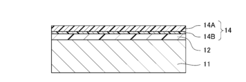
- the semiconductor substrate 11 having the foreign matter removing coating film 12 shown in Fig. 1B and the supporting base material 14 having the flexible support 14A and the adhesive layer 14B are arranged so that the foreign matter removing coating film 12 and the adhesive layer 14B face each other, and are bonded together (Fig. 1C).
- the supporting base material 14 has optical transparency.
- the surface of the semiconductor substrate 11 opposite to the surface on which the foreign matter removing coating film 12 is disposed is polished to thin the semiconductor substrate 11 (FIG. 1D).
- the coating film 12 for removing foreign matter is irradiated with light L from the side of the supporting substrate 14 (FIG. 1E).
- the cross-linked structure of the coating film 12 for removing foreign matter is decomposed by the light irradiation.
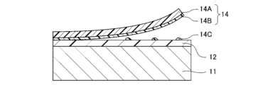
- the support base 14 is separated from the semiconductor substrate 11 (FIGS. 1F and 1G). After separation, peeling residue 14C of adhesive layer 14B remains on foreign matter removal coating film 12 (FIG. 1G). Therefore, foreign matter removal coating film 12 is removed with a removal liquid (FIG. 1H). By doing so, peeling residue 14C, which is a foreign matter, can be prevented from remaining on semiconductor substrate 11.
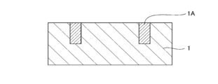
- a semiconductor substrate 1 having wiring 1A is prepared (FIG. 2A).
- a coating film 2 for removing foreign matter is formed on the semiconductor substrate 1 (FIG. 2B).
- the coating film 2 for removing foreign matter has a cross-linked structure due to an acetal structure.
- a glass substrate 4 having an adhesive layer 3 formed on its surface is prepared (FIG. 2C).
- the adhesive layer 3 and the glass substrate 4 are optically transparent.
- FIGS. 2C and 2E are arranged so that the foreign matter removal coating film 2 and the adhesive layer 3 face each other, and are bonded together.
- FIG. 2F the surface of the semiconductor substrate 1 opposite to the surface on which the coating film 2 for removing foreign matter is polished to thin the semiconductor substrate 1 (FIG. 2F), thereby exposing the wiring 1A.
- the laminate shown in FIG. 2F and a second semiconductor substrate 5 having wiring 5A are arranged so that the surface of the semiconductor substrate 1 opposite to the surface of the coating film 2 for removing foreign matter faces the surface of the second semiconductor substrate 5 on which the wiring 5A is exposed, and are bonded together (FIGS. 2G and 2H).
- the manufacturing method of the processed semiconductor substrate of the present invention can be suitably used for hybrid bonding to connect semiconductor substrates together.
- Example 1 Preparation of protective film-forming composition> 0.51 g of polyhydroxystyrene (product name VP-8000), 0.25 g of triethylene glycol divinyl ether, 0.01 g of oxalic acid, and 0.04 g of a photoacid generator CPI-110TF (manufactured by San-Apro) were added to 9.6 g of propylene glycol monomethyl ether and 9.6 g of propylene glycol monomethyl ether acetate, and the mixture was stirred at room temperature for 30 minutes to prepare a composition for forming a protective film [1].
- polyhydroxystyrene product name VP-8000
- triethylene glycol divinyl ether 0.01 g of oxalic acid
- a photoacid generator CPI-110TF manufactured by San-Apro
- the protective film-forming composition [1] was applied onto a semiconductor substrate (silicon wafer) using a spinner, and then baked on a hot plate at a temperature of 190° C. for 90 seconds to form a protective film with a thickness of 113 nm.
- the resulting protective film was insoluble in propylene glycol monomethyl ether.
- the resulting protective film was insoluble in propylene glycol monomethyl ether acetate.
- the obtained protective film was insoluble in a 2.38% by mass aqueous solution of tetramethylammonium hydroxide (manufactured by Tokyo Ohka Kogyo Co., Ltd., product name NMD-3).
- the protective film-forming composition [1] was applied onto a silicon wafer using a spinner, and then baked for 60 seconds at a temperature of 190°C using a hot plate to form a protective film with a thickness of 113 nm.
- the obtained protective film was exposed to ultraviolet light having a wavelength of 365 nm at 500 mJ/ cm2 using an ultraviolet irradiation device PLA-501 manufactured by Canon Inc.
- Paddle development was performed for 60 seconds using a 2.38 mass% aqueous solution of tetramethylammonium hydroxide (manufactured by Tokyo Ohka Kogyo Co., Ltd., product name NMD-3) as an alkaline removal solution, and the product was washed with pure water. The protective film was dissolved, and no residual film was observed.
- tetramethylammonium hydroxide manufactured by Tokyo Ohka Kogyo Co., Ltd., product name NMD-3
- Example 2 ⁇ Preparation of protective film-forming composition>> 0.63 g of polyhydroxystyrene (product name VP-8000), 0.13 g of 1,4-cyclohexanedimethanol divinyl ether, and 0.04 g of a photoacid generator CPI-110TF (manufactured by San-Apro) were added to 9.6 g of propylene glycol monomethyl ether and 9.6 g of propylene glycol monomethyl ether acetate, and the mixture was stirred at room temperature for 30 minutes to prepare a composition for forming a protective film [2].
- the protective film-forming composition [2] was applied onto a semiconductor substrate (silicon wafer) using a spinner, and then baked on a hot plate at a temperature of 190° C. for 90 seconds to form a protective film with a thickness of 123 nm.
- the resulting protective film was insoluble in propylene glycol monomethyl ether.
- the resulting protective film was insoluble in propylene glycol monomethyl ether acetate.
- the obtained protective film was insoluble in a 2.38% by mass aqueous solution of tetramethylammonium hydroxide (manufactured by Tokyo Ohka Kogyo Co., Ltd., product name NMD-3).
- the protective film forming composition [2] was applied onto a silicon wafer using a spinner, and then baked for 60 seconds at 190°C using a hot plate to form a protective film with a thickness of 123 nm.
- the obtained protective film was exposed to 500 mJ/ cm2 ultraviolet light with a wavelength of 365 nm using a Canon Inc. ultraviolet irradiation device PLA-501.
- Paddle development was performed for 60 seconds using a 2.38 mass% aqueous solution of tetramethylammonium hydroxide (manufactured by Tokyo Ohka Kogyo Co., Ltd., product name NMD-3) as an alkaline removal solution, and the product was washed with pure water. The protective film was dissolved, and no residual film was observed.
- tetramethylammonium hydroxide manufactured by Tokyo Ohka Kogyo Co., Ltd., product name NMD-3
- Example 3 Preparation of protective film-forming composition> 0.63 g of polyhydroxystyrene (product name VP-8000), 0.13 g of trimethylolpropane trivinyl ether, and 0.04 g of a photoacid generator CPI-110TF (manufactured by San-Apro) were added to 9.6 g of propylene glycol monomethyl ether and 9.6 g of propylene glycol monomethyl ether acetate, and the mixture was stirred at room temperature for 30 minutes to prepare a composition for forming a protective film [3].
- polyhydroxystyrene product name VP-8000
- CPI-110TF photoacid generator
- the protective film-forming composition [3] was applied onto a semiconductor substrate (silicon wafer) using a spinner, and then baked on a hot plate at a temperature of 190° C. for 90 seconds to form a protective film with a thickness of 123 nm.
- the resulting protective film was insoluble in propylene glycol monomethyl ether.
- the resulting protective film was insoluble in propylene glycol monomethyl ether acetate.
- the obtained protective film was insoluble in a 2.38% by mass aqueous solution of tetramethylammonium hydroxide (manufactured by Tokyo Ohka Kogyo Co., Ltd., product name NMD-3).
- the protective film-forming composition [3] was applied onto a silicon wafer using a spinner, and then baked for 60 seconds at a temperature of 190°C using a hot plate to form a protective film with a thickness of 123 nm.
- the obtained protective film was exposed to ultraviolet light of a wavelength of 365 nm at 500 mJ/ cm2 using an ultraviolet irradiation device PLA-501 manufactured by Canon Inc.
- Paddle development was performed for 60 seconds using a 2.38 mass% aqueous solution of tetramethylammonium hydroxide (manufactured by Tokyo Ohka Kogyo Co., Ltd., product name NMD-3) as an alkaline removal solution, and the film was washed with pure water. The protective film was dissolved, and no residual film was observed.
- tetramethylammonium hydroxide manufactured by Tokyo Ohka Kogyo Co., Ltd., product name NMD-3
- Example 4 Preparation of protective film-forming composition> A composition for forming a protective film [4] was prepared in the same manner as in Example 1, except that 0.04 g of the photoacid generator CPI-110TF (manufactured by San-Apro) in Example 1 was changed to 0.04 g of the photoacid generator CPI-210S (manufactured by San-Apro).
- the protective film-forming composition [4] was applied onto a semiconductor substrate (silicon wafer) using a spinner, and then baked on a hot plate at a temperature of 190° C. for 90 seconds to form a protective film with a thickness of 111 nm.
- the resulting protective film was insoluble in propylene glycol monomethyl ether.
- the resulting protective film was insoluble in propylene glycol monomethyl ether acetate.
- the obtained protective film was insoluble in a 2.38% by mass aqueous solution of tetramethylammonium hydroxide (manufactured by Tokyo Ohka Kogyo Co., Ltd., product name NMD-3).
- the protective film-forming composition [4] was applied onto a silicon wafer using a spinner, and then baked for 60 seconds at a temperature of 190°C using a hot plate to form a protective film with a thickness of 111 nm.
- the obtained protective film was exposed to 500 mJ/ cm2 ultraviolet light with a wavelength of 365 nm using a Canon Inc. ultraviolet irradiation device PLA-501.
- Paddle development was performed for 60 seconds using a 2.38 mass% aqueous solution of tetramethylammonium hydroxide (manufactured by Tokyo Ohka Kogyo Co., Ltd., product name NMD-3) as an alkaline removal solution, and the product was washed with pure water. The protective film was dissolved, and no residual film was observed.
- tetramethylammonium hydroxide manufactured by Tokyo Ohka Kogyo Co., Ltd., product name NMD-3
- Example 5 Preparation of protective film-forming composition> A composition for forming a protective film [5] was prepared in the same manner as in Example 1, except that 0.04 g of the photoacid generator CPI-110TF (manufactured by San-Apro) in Example 1 was changed to 0.04 g of the photoacid generator CPI-310MS (manufactured by San-Apro).
- ⁇ Solubility after exposure to light in alkaline removal solution>> In the same manner as in the evaluation of ⁇ Solubility after exposure to light in an alkaline removal solution>> in Example 4, the ⁇ Solubility after exposure to light in an alkaline removal solution>> was evaluated for a protective film having a thickness of 111 nm formed from the protective film-forming composition [5]. As a result, the protective film was dissolved and no residual film was observed.
- Example 6 Preparation of protective film-forming composition> A composition for forming a protective film [6] was prepared in the same manner as in Example 1, except that 0.04 g of the photoacid generator CPI-110TF (manufactured by San-Apro) in Example 1 was changed to 0.04 g of the photoacid generator CPI-310CS (manufactured by San-Apro).
- ⁇ Solubility after exposure to light in alkaline removal solution>> In the same manner as in the evaluation of ⁇ Solubility after exposure to light in an alkaline removal solution>> in Example 4, the ⁇ Solubility after exposure to light in an alkaline removal solution>> was evaluated for a protective film having a thickness of 111 nm formed from the protective film-forming composition [6]. As a result, the protective film was dissolved and no residual film was observed.
Landscapes
- Chemical & Material Sciences (AREA)
- Organic Chemistry (AREA)
- Engineering & Computer Science (AREA)
- Life Sciences & Earth Sciences (AREA)
- Materials Engineering (AREA)
- Wood Science & Technology (AREA)
- Medicinal Chemistry (AREA)
- Chemical Kinetics & Catalysis (AREA)
- Health & Medical Sciences (AREA)
- Polymers & Plastics (AREA)
- Physics & Mathematics (AREA)
- Spectroscopy & Molecular Physics (AREA)
- General Physics & Mathematics (AREA)
- Materials For Photolithography (AREA)
- Compositions Of Macromolecular Compounds (AREA)
- Paints Or Removers (AREA)
- Manufacturing & Machinery (AREA)
Abstract
Description
また、本発明は、当該保護膜形成用組成物から形成される保護膜、当該保護膜を有する半導体基板又は電子部品、及び当該保護膜を用いた加工された半導体基板の製造方法を提供することを目的とする。
すなわち、本発明は以下を包含する。
[1] フェノール性ヒドロキシ基及びカルボキシ基の少なくともいずれかを有するポリマー(A)、ビニルエーテル基含有架橋剤(B)、光酸発生剤(C)及び溶剤(D)を含む、保護膜形成用組成物。
[2] 前記ポリマー(A)が、ヒドロキシスチレンに由来する繰り返し単位を有する、[1]に記載の保護膜形成用組成物。
[3] 半導体基板を異物から保護する保護膜である異物除去用コーティング膜を形成するための組成物である、[1]又は[2]に記載の保護膜形成用組成物。
[4] 電子部品の傷つき防止又は破損防止のための保護膜を形成するための組成物である、[1]又は[2]に記載の保護膜形成用組成物。
[5] 反射防止膜形成用組成物ではない、[1]から[4]のいずれかに記載の保護膜形成用組成物。
[6] 前記ビニルエーテル基含有架橋剤(B)が、下記式(VE)で表される化合物である、[1]から[5]のいずれかに記載の保護膜形成用組成物。
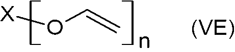
[7] 前記ビニルエーテル基含有架橋剤(B)が、下記式(VE-1)で表される化合物、下記式(VE-2)で表される化合物、及び下記式(VE-3)で表される化合物の少なくともいずれかである、[1]から[6]のいずれかに記載の保護膜形成用組成物。

式(VE-2)中、R2は、3価の有機基を表す。
式(VE-3)中、R3は、それぞれ独立して、2価の有機基を表す。n1は、2~6の整数を表す。)
[8] [1]から[7]のいずれかに記載の保護膜形成用組成物から形成された保護膜。
[9] [8]に記載の保護膜を有する半導体基板。
[10] [8]に記載の保護膜を有する電子部品。
[11] 加工された半導体基板の製造方法であって、
[9]に記載の半導体基板と支持基材とを、前記保護膜である異物除去用コーティング膜を介して貼り合わせて積層体を製造する第1工程と、
該積層体を加工する第2工程と、
前記異物除去用コーティング膜に光を照射する第3工程と、
該積層体から前記支持基材を剥離する第4工程と、
前記半導体基板又は前記支持基材を除去液で洗浄して、前記異物除去用コーティング膜を除去する第5工程とを含む、加工された半導体基板の製造方法。
[12] 前記第5工程で前記異物除去用コーティング膜とともに異物を除去する、[11]に記載の加工された半導体基板の製造方法。
[13] 前記第1工程が、前記半導体基板と前記支持基材とを、前記異物除去用コーティング膜及び接着剤層を介して貼り合わせて積層体を製造する工程である、[11]又は[12]に記載の加工された半導体基板の製造方法。
[14] 前記第5工程で前記異物除去用コーティング膜と共に、前記接着剤層の剥離残渣である異物を除去する、[13]に記載の半導体基板の製造法方法。
[15] 前記加工が、前記半導体基板と第2の半導体基板とを接続することを含む、[11]から[14]のいずれかに記載の加工された半導体基板の製造方法。
[16] 前記第3工程が、前記第4工程の後かつ前記第5工程の前に行われる、[11]から[15]のいずれかに記載の加工された半導体基板の製造方法。
また、本発明は、当該保護膜形成用組成物から形成される保護膜、当該保護膜を有する半導体基板又は電子部品、及び当該保護膜を用いた加工された半導体基板の製造方法を提供することができる。
本発明の保護膜形成用組成物は、ポリマー(A)、架橋剤(B)、光酸発生剤(C)及び溶剤(D)を含む。
ポリマー(A)は、フェノール性ヒドロキシ基及びカルボキシ基の少なくともいずれかを有する。
架橋剤(B)は、少なくとも2つのビニルエーテル基を有する。以下、架橋剤(B)を、ビニルエーテル基含有架橋剤(B)と称することがある。
保護膜形成用組成物は、その他の成分として、アセタール化触媒(E)を含んでいてもよい。
他方、架橋構造を有する保護膜に光を照射すると、光酸発生剤から発生した酸によるアセタール構造の分解により架橋構造が分解される。その結果、光が照射された後の保護膜は、溶剤(例えば、有機溶剤やアルカリ性除去液)に溶解しやすくなる。そのため、保護膜の除去が容易となる。
光の波長としては、特に制限されず、例えば、210nm~440nmが挙げられる。
光源としては、例えば、えば、低圧水銀ランプ(殺菌ランプ、蛍光ケミカルランプ、ブラックライト)、高圧放電ランプ(高圧水銀ランプ、メタルハライドランプ)、ショートアーク放電ランプ(超高圧水銀ランプ、キセノンランプ、水銀キセノンランプ)、発光ダイオード(light-emitting diode;LED)などが挙げられる。
照射量としては、特に制限されず、例えば、5mJ/cm2~1,000mJ/cm2が挙げられる。
保護膜形成用組成物は、好ましくは、電子部品の傷つき防止又は破損防止のための保護膜を形成するための組成物である。
例えば、本発明の保護膜形成用組成物は、WO2005/111724に記載の反射防止膜形成用組成物ではない。
ポリマー(A)は、フェノール性ヒドロキシ基及びカルボキシ基の少なくともいずれかを有する。
%である。

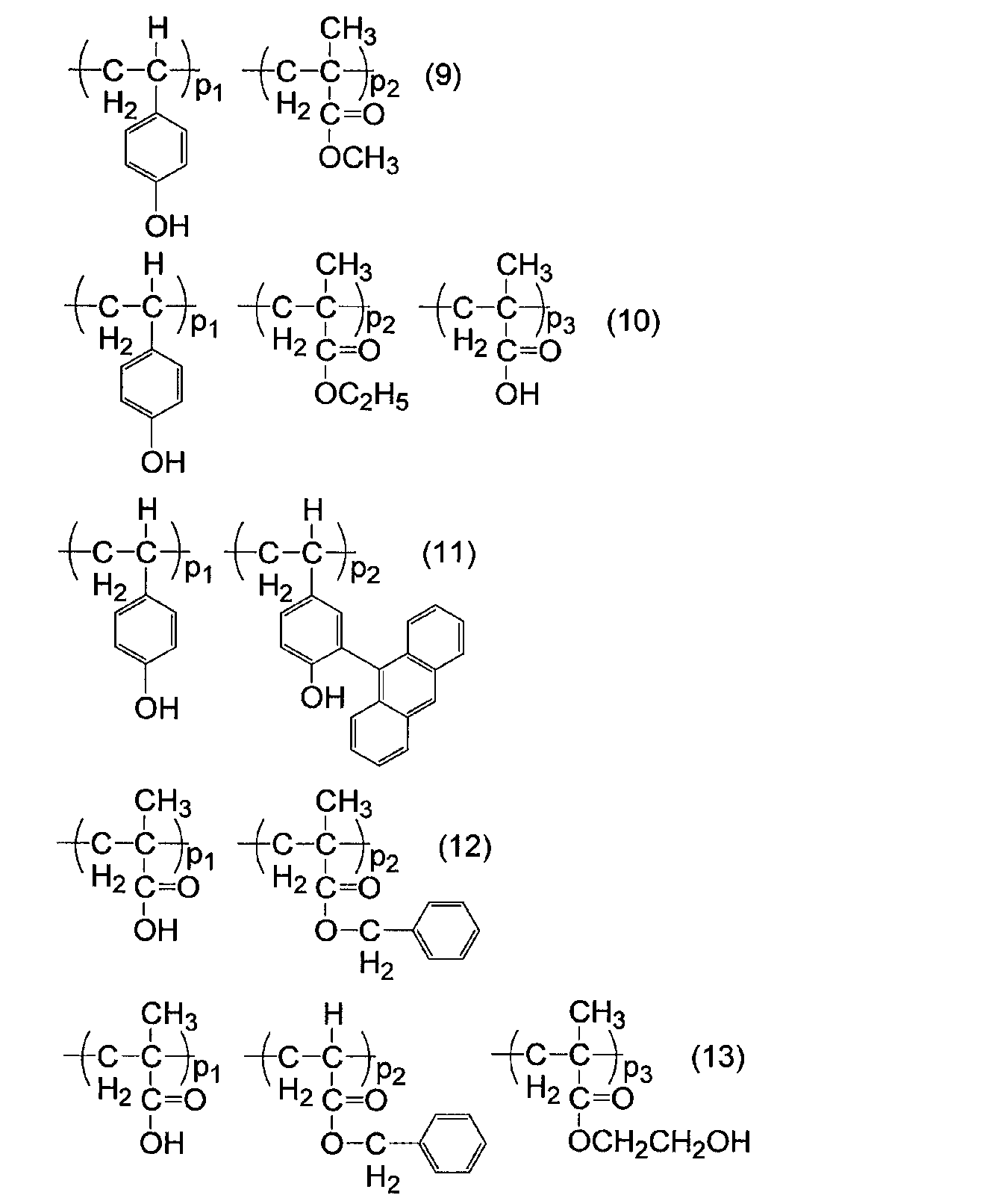


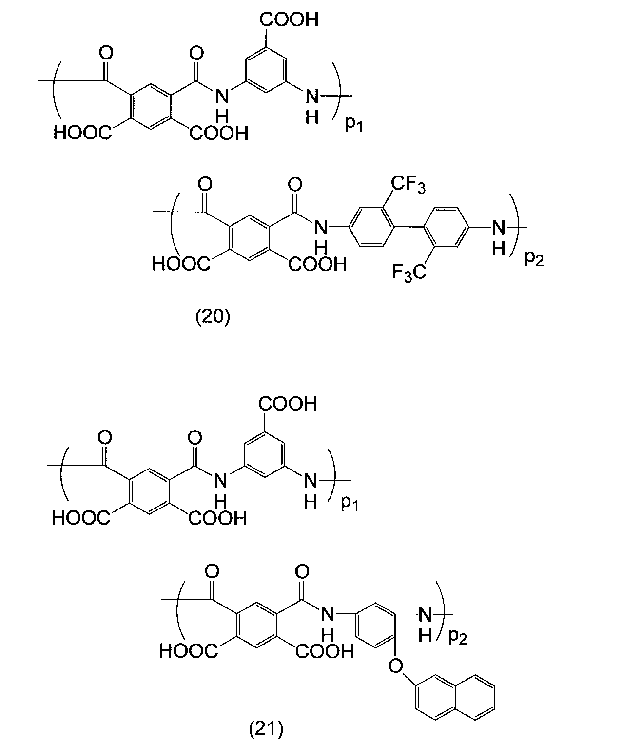
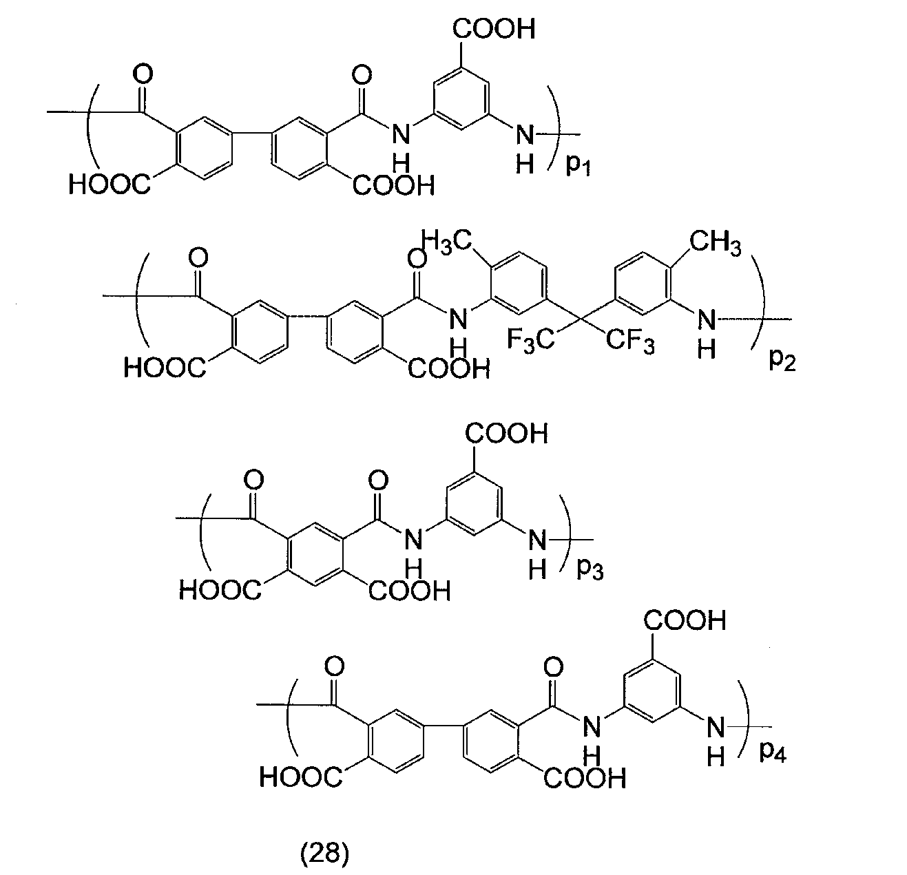

このようなポリマーは、少なくとも二つのエポキシ基を有する化合物とエポキシ基に対してほぼ等モル量の少なくとも二つのフェノール性ヒドロキシ基又はカルボキシル基を有する化合物を、四級アンモニウム塩等の触媒存在下において反応させることにより製造することができる。
少なくとも二つのエポキシ基を有する化合物としては、例えば、トリス(2,3-エポキシプロピル)イソシアヌレート、1,4-ブタンジオールジグリシジルエーテル、1,2-エポキシ-4-(エポキシエチル)シクロヘキサン、グリセロールトリグリシジルエーテル、ジエチレングリコールジグリシジルエーテル、2,6-ジグリシジルフェニルグリシジルエーテル、1,1,3-トリス[p-(2,3-エポキシプロポキシ)フェニル]プロパン、1,2-シクロヘキサンジカルボン酸ジグリシジルエステル、4,4’-メチレンビス(N,N-ジグリシジルアニリン)、3,4-エポキシシクロヘキシルメチル-3,4-エポキシシクロヘキサンカルボキシレート、トリメチロールエタントリグリシジルエーテル、ビスフェノール-A-ジグリシジルエーテル、及びペンタエリスリトールポリグリシジルエーテル等を挙げることができる。
少なくとも二つのフェノール性ヒドロキシ基又はカルボキシル基を有する化合物としては、例えば、1,2,3-アントラセントリオール、2,7,9-アントラセントリオール、2-ヒドロキシ-1-ナフトエ酸、7-ヒドロキシ-1-ナフトエ酸、3-ヒドロキシ-2-ナフトエ酸、2,6-ナフトエ酸、1-ヒドロキシ-4-フェニル-3-ナフトエ酸、6-エトキシ-2,3-ナフタレンジオール、4-ヒドロキシ安息香酸、2-クロロ-4-ヒドロキシ安息香酸、2,4-ジヒドロキシ-5-メチル安息香酸、3-ヒドロキシ安息香酸、5-ヒドロキシイソフタル酸、2,5-ジヒドロキシ安息香酸、テレフタル酸、2-ニトロテレフタル酸、3,5-ジブロモ-4-ヒドロキシ安息香酸、3,5-ジブロモ-2,4-ジヒドロキシ安息香酸、3-ヨ-ド-5-ニトロ-4-ヒドロキシ安息香酸、3,5-ジヨード-2-ヒドロキシ安息香酸、2,4,6-トリヨード-3-ヒドロキシ安息香酸、2,4,6-トリブロモ-3-ヒドロキシ安息香酸、及び2-ブロモ-4,6-ジメチル-3-ヒドロキシ安息香酸等が挙げられる。
少なくとも二つのエポキシ基を有する化合物と少なくとも二つのフェノール性ヒドロキシ基又はカルボキシル基を有する化合物とから製造されるポリマーとしては、例えば、式(43)のポリマーが挙げられる。

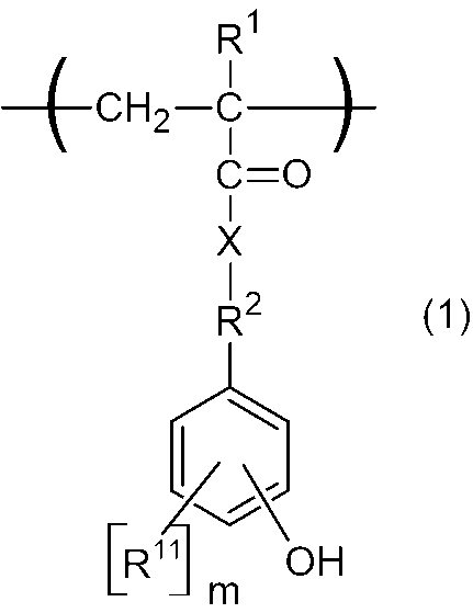
光が照射された後の保護膜のアルカリ性除去液に対する溶解性の点から、式(1)のユニットはポリマーを構成する全ユニットに対して、例えば、10%以上のモル割合で含まれる。ポリマーにおける式(1)のユニットのモル割合は10%以上、好ましくは20%以上であり、例えば10%~100%、好ましくは15%~80%、より好ましくは20%~70%、最も好ましくは25%~50%である。
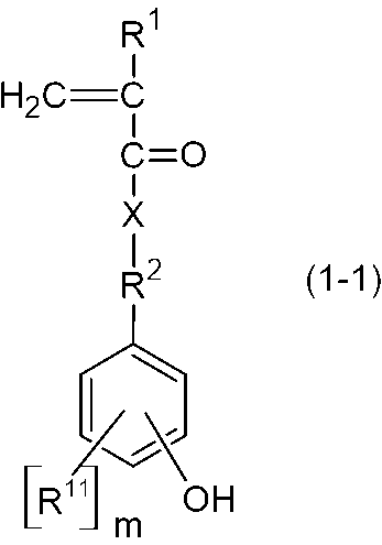

ここで固形分とは、保護膜形成用組成物の全成分から溶剤成分を除いたものである。
ビニルエーテル基含有架橋剤(B)としては、2つ以上のビニルエーテル基を有する化合物であれば、特に制限されない。
ビニルエーテル基含有架橋剤(B)が有するビニルエーテル基の数としては、2つ以上であれば特に制限されず、例えば、2つ~8つであってもよいし、2つ~6つであってもよいし、2つ~4つであってもよい。
ビニルエーテル基含有架橋剤(B)の分子量としては、特に制限されず、例えば、100~1,000であってもよいし、100~800であってもよいし、100~550であってもよい。
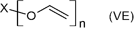
Xは、ヘテロ原子を有していてもよい。ヘテロ原子としては、例えば、酸素原子、窒素原子、硫黄原子などが挙げられる。
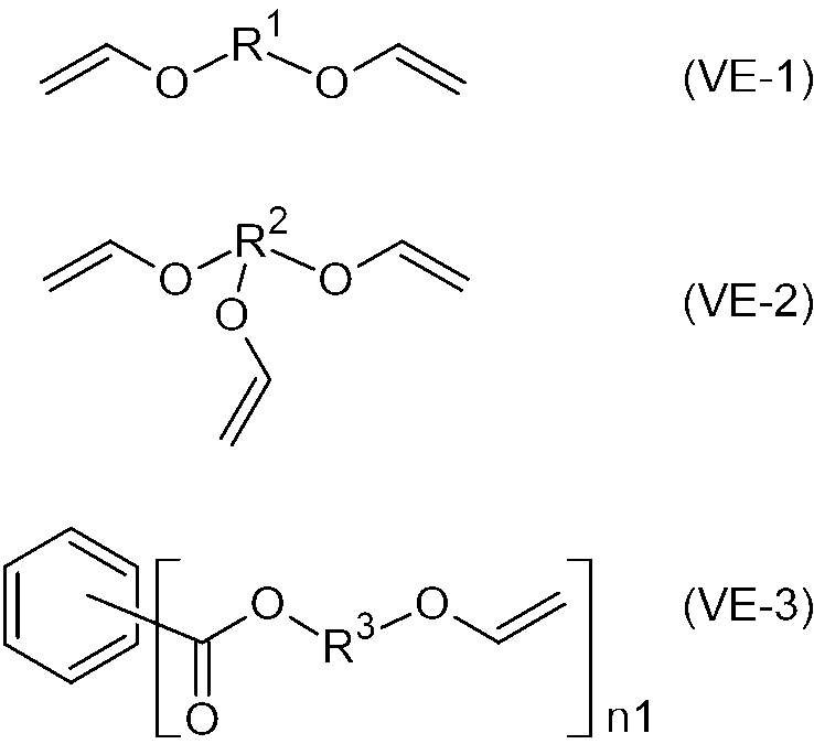
式(VE-2)中、R2は、3価の有機基を表す。
式(VE-3)中、R3は、それぞれ独立して、2価の有機基を表す。n1は、2~6の整数を表す。)
式(VE-1)で表される化合物としては、例えば、下記式(VE-1-1)~式(VE-1-3)の化合物などが挙げられる。
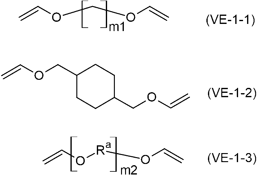
式(VE-1-3)中、Raは、エチレン基、又はプロピレン基を表す。m2は、2~6の整数を表す。)
式(VE-1-3)中のRaは、1,2-エチレン基であってもよいし、1,3-プロピレン基であってもよいし、1,2-プロピレン基であってもよい。
式(VE-1-3)中のm2は、2であってもよいし、3であってもよいし、4であってもよいし、5であってもよいし、6であってもよい。
式(VE-2)中のR2としては、例えば、飽和炭化水素基などが挙げられる。
式(VE-3)中のR3としては、例えば、-(CH2)m1-(m1は1~10の整数を表す。)、-(CH2O)m2-1-CH2-(m2は1~10の整数を表す。)などが挙げられる。m1及びm2は、それぞれ独立して、1~6の整数であってもよいし、2~6の整数であってもよいし、3~5の整数であってもよい。
式(VE-3)で表される化合物としては、例えば、下記式(VE-3-1)~式(VE-3-6)の化合物が挙げられる。
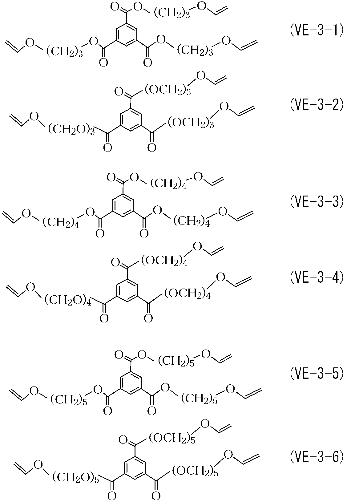
光酸発生剤(C)としては、露光に使用される光の照射によって酸を発生する化合物が挙げられる。例えば、ジアゾメタン化合物、オニウム塩化合物、スルホンイミド化合物、ニトロベンジル化合物、ベンゾイントシレート化合物、ハロゲン含有トリアジン化合物、及びシアノ基含有オキシムスルホネート化合物等の光酸発生剤が挙げられる。これらの中でオニウム塩化合物の光酸発生剤が好適である。
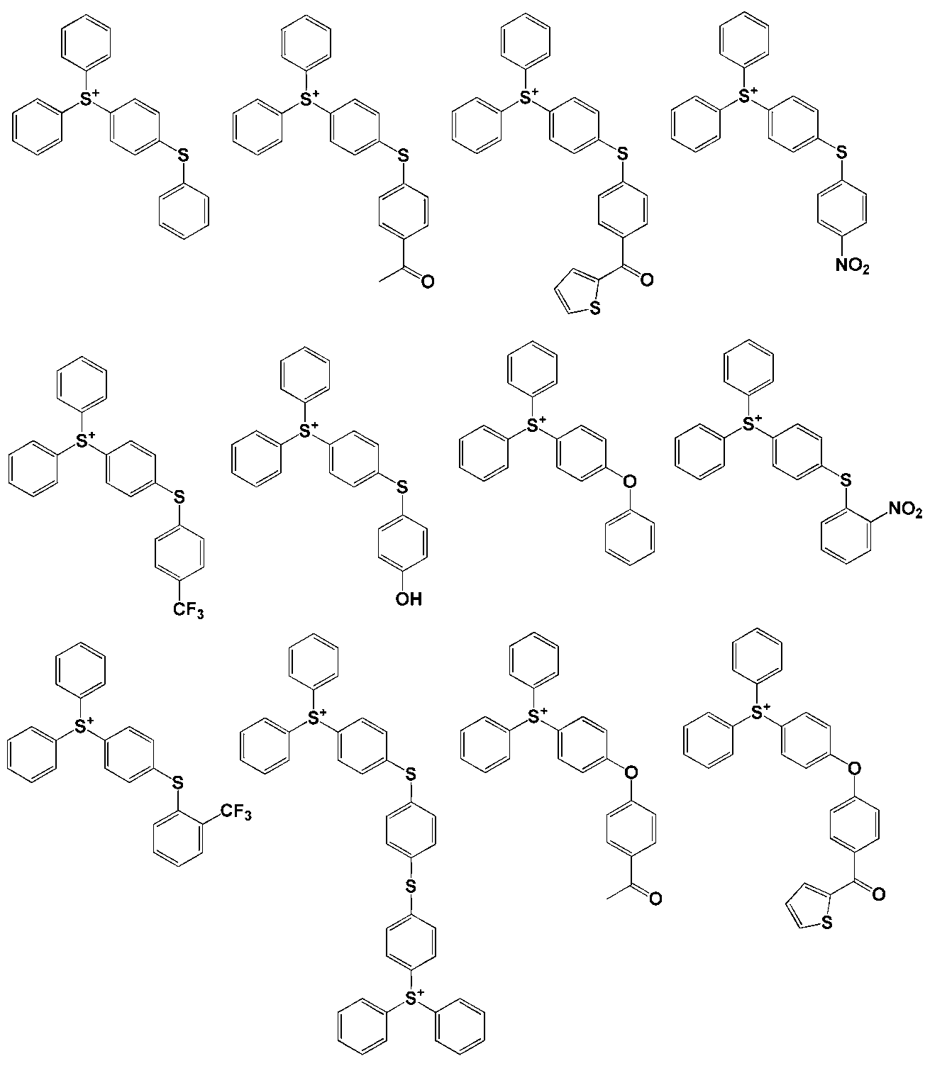

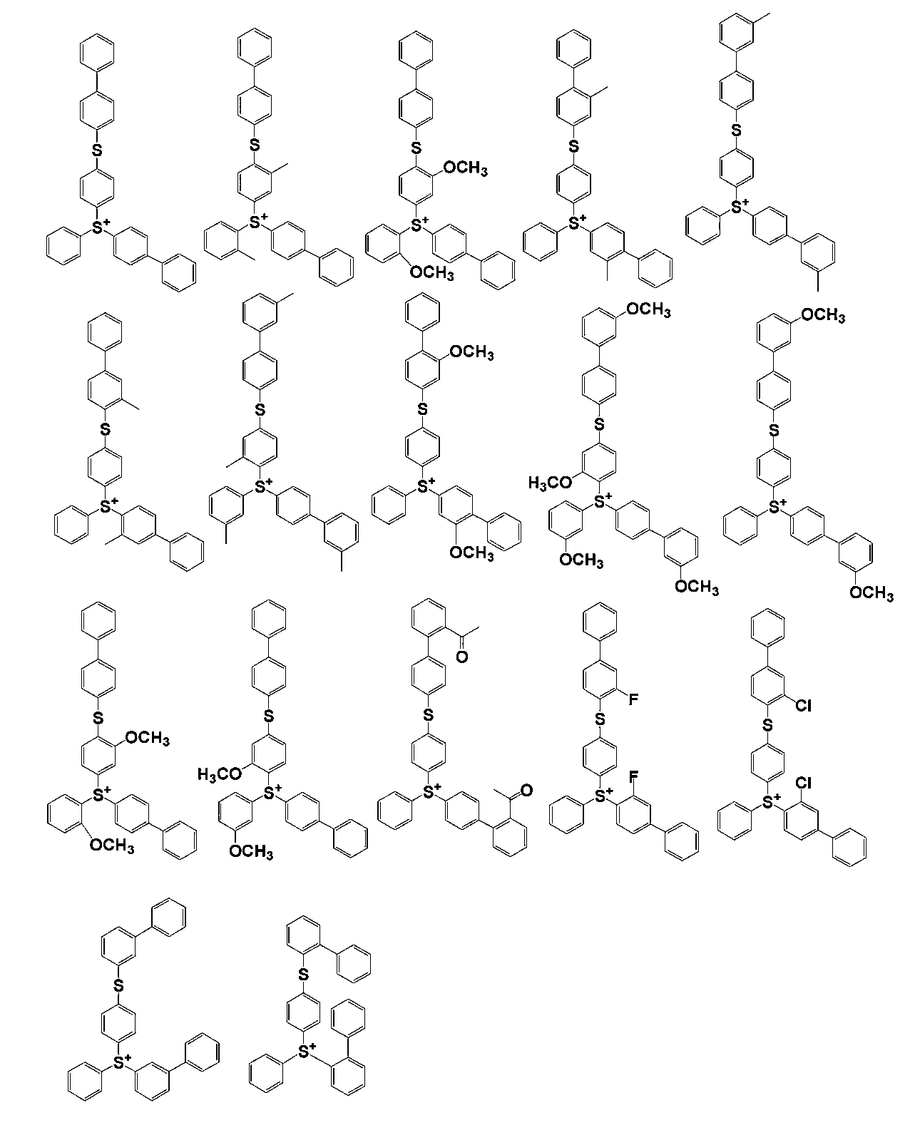
・MYa -
・(Rf)bPF6-b -
・Rx1 cBY4-c -
・Rx2SO3 -
・(Rx2SO2)3C-
・(Rx2SO2)2N-
Yはハロゲン原子(フッ素原子が好ましい。)を表す。
また、Rx2で表されるアルキル基、フルオロアルキル基又はアリール基における炭素鎖は、酸素原子、窒素原子、硫黄原子等のヘテロ原子を有していてもよい。特に、Rx2で表されるアルキル基又はフルオロアルキル基における炭素鎖は、2価の官能基(例えば、エーテル結合、カルボニル結合、エステル結合、アミノ結合、アミド結合、イミド結合、スルホニル結合、スルホニルアミド結合、スルホニルイミド結合、ウレタン結合等)を有していてもよい。
Rx2で表されるアルキル基、フルオロアルキル基又はアリール基が上記置換基、ヘテロ原子、又は官能基を有する場合、上記置換基、ヘテロ原子、又は官能基の個数は、1個であっても2個以上であってもよい。
aは4以上6以下の整数を表す。
bは、1以上5以下の整数が好ましく、さらに好ましくは2以上4以下の整数、特に好ましくは2又は3である。
cは、1以上4以下の整数が好ましく、さらに好ましくは4である。
Rx1 cBY4-c -
(式中、Rx1は水素原子の少なくとも一部がハロゲン原子又は電子求引基で置換されたフェニル基を示し、Yはハロゲン原子を示し、cは1以上4以下の整数を示す。)
であり、例えば、((C6F5)4B)-、(((CF3)2C6H3)4B)-、((CF3C6H4)4B)-、((C6F5)2BF2)-、(C6F5BF3)-又は((C6H3F2)4B)-で表されるアニオン等が挙げられる。これらのうち、((C6F5)4B)-又は(((CF3)2C6H3)4B)-で表されるアニオンが好ましい。
溶剤(D)としては、例えば、エチレングリコールモノメチルエーテル、エチレングリコールモノエチルエーテル、メチルセロソルブアセテート、エチルセロソルブアセテート、ジエチレングリコールモノメチルエーテル、ジエチレングリコールモノエチルエーテル、プロピレングリコール、プロピレングリコールモノメチルエーテル、プロピレングリコールモノメチルエーテルアセテート、プロピレングリコールプロピルエーテルアセテート、トルエン、キシレン、メチルエチルケトン、シクロペンタノン、シクロヘキサノン、2-ヒドロキシプロピオン酸エチル、2-ヒドロキシ-2-メチルプロピオン酸エチル、エトキシ酢酸エチル、ヒドロキシ酢酸エチル、2-ヒドロキシ-3-メチルブタン酸メチル、3-メトキシプロピオン酸メチル、3-メトキシプロピオン酸エチル、3-エトキシプロピオン酸エチル、3-エトキシプロピオン酸メチル、ピルビン酸メチル、ピルビン酸エチル、酢酸エチル、酢酸ブチル、乳酸エチル、乳酸ブチル、N,N-ジメチルホルムアミド、N,N-ジメチルアセトアミド、N-メチルピロリドン等を用いることができる。
これらの溶剤は単独または2種以上の組合せで使用することができる。
さらに、プロピレングリコールモノブチルエーテル、プロピレングリコールモノブチルエーテルアセテート等の高沸点溶剤を混合して使用することができる。
このように調製された保護膜形成用組成物は、孔径が0.2μm程度のフィルタなどを用いて濾過した後、使用に供することが好ましい。このように調製された保護膜形成用組成物は、室温で長期間の貯蔵安定性にも優れる。
ポリマー(A)におけるフェノール性ヒドロキシ基又はカルボキシ基と、ビニルエーテル基含有架橋剤(B)におけるビニルエーテル基との反応(アセタール化反応)のための触媒として、保護膜形成用組成物はアセタール化触媒(E)を含んでいてもよい。
ポリマー(A)におけるフェノール性ヒドロキシ基又はカルボキシ基と、ビニルエーテル基含有架橋剤(B)におけるビニルエーテル基との組み合わせによっては、保護膜形成用組成物はアセタール化触媒(E)を含んでいなくてもよい。
酸としては、例えば、有機酸、無機酸が挙げられる。
有機酸としては、例えば、脂肪族モノカルボン酸、脂肪族多価カルボン酸、芳香族カルボン酸、芳香族スルホン酸またはその塩などが挙げられる。
無機酸としては、例えば、硫酸塩、硫酸水素塩、鉱酸、ヘテロポリ酸などが挙げられる。
脂肪族多価カルボン酸としては、例えば、シュウ酸、マレイン酸、コハク酸、マロン酸、フマル酸、酒石酸、クエン酸などが挙げられる。
芳香族カルボン酸としては、例えば、安息香酸、テレフタル酸などが挙げられる。
芳香族スルホン酸またはその塩としては、例えば、ベンゼンスルホン酸、p-トルエンスルホン酸、p-トルエンスルホン酸ピリジニウム塩、p-トルエンスルホン酸キノリニウム塩などが挙げられる。
硫酸水素塩としては、例えば、硫酸水素ナトリウム、硫酸水素カリウムなどが挙げられる。
鉱酸としては、例えば、硫酸、塩酸、リン酸、ポリリン酸などが挙げられる。
ヘテロポリ酸としては、例えば、リンバナドモリブデン酸、リンタングストモリブデン酸、ケイタングストモリブデン酸などが挙げられる。
保護膜形成用組成物は、添加剤として、吸光性化合物、界面活性剤、接着補助剤、レオロジー調整剤、シリカ粒子などを含むことができる。
異物除去用コーティング膜は、光照射された後に除去液によって除去可能な膜である。
保護膜は、例えば、半導体基板上又は電子部品上に形成される。その場合の除去としては、半導体基板上又は電子部品上から除去されることを指す。
ここで、除去の態様としては、溶解除去、剥離除去などが挙げられる。剥離除去としては、例えば、膨潤によって被着物から剥離することが挙げられる。
除去液は、有機溶剤を50質量%以上含む除去液であってもよい。
アルカリ性除去液は、半導体製造プロセスで用いられる現像液又は洗浄液であり、かつアルカリ性を示すものでもよい。例えば、現像液として、NMD-3(2.38%テトラメチルアンモニウムヒドロキシド水溶液、東京応化工業株式会社製)が挙げられる。
無機アルカリ化合物としては、例えば、水酸化カリウム、水酸化ナトリウム、水酸化リチウム、リン酸水素二アンモニウム、リン酸水素二カリウム、リン酸水素二ナトリウム、ケイ酸リチウム、ケイ酸ナトリウム、ケイ酸カリウム、炭酸リチウム、炭酸ナトリウム、炭酸カリウム、ホウ酸リチウム、ホウ酸ナトリウム、ホウ酸カリウム等などが挙げられる。
水酸化四級アンモニウムとしては、例えば、水酸化テトラメチルアンモニウム、水酸化テトラエチルアンモニウム、トリメチルヒドロキシエチルアンモニウムヒドロキシド、コリンなどが挙げられる。
アミンとしては、例えば、エタノールアミン、メチルアミン、ジメチルアミン、トリメチルアミン、モノエチルアミン、ジエチルアミン、トリエチルアミン、n-プロピルアミン、ジ-n-プロピルアミン、イソプロピルアミン、ジイソプロピルアミン、メチルジエチルアミン、ジメチルエタノールアミン、トリエタノールアミン、エチレンジアミンなどが挙げられる。
ヒドラジンとしては、例えばヒドラジン一水和物などが挙げられる。
また、アルカリ性除去液は、SC-1(アンモニア-過酸化水素溶液)であってもよい。
酸性除去液は、例えば、希フッ酸を含む水溶液である。
また、酸性除去液は、例えば、硫酸及び過酸化水素を含む水溶液であってもよいし、酢酸又はキレート剤を含む水溶液であってもよい。キレート剤としては、例えば、有機酸、有機酸の塩、アミノ酸、アミノ酸の誘導体などが挙げられる。
本発明の保護膜は、本発明の保護膜形成用組成物から形成される。
半導体基板の上に、スピナー、コーター、浸漬等の適当な塗布方法により本発明の異物除去用コーティング膜形成組成物が塗布され、その後、焼成することにより異物除去用コーティング膜が形成される。焼成する条件としては、焼成温度80℃~300℃、焼成時間0.3~60分間の中から適宜、選択される。
この際に、ポリマー(A)におけるフェノール性ヒドロキシ基又はカルボキシ基と、ビニルエーテル基含有架橋剤(B)におけるビニルエーテル基との反応(アセタール化反応)によってアセタール構造が形成される。その結果、架橋構造を有する保護膜が形成される。
本発明の半導体基板は、その上に本発明の保護膜を有する。
ここでの保護膜は、通常、架橋構造を有する保護膜であって、光照射前の保護膜である。
半導体基板の形状は、特に限定されないが、例えば、円盤状である。なお、円盤状の半導体基板は、その面の形状が完全な円形である必要はなく、例えば、半導体基板の外周は、オリエンテーション・フラットと呼ばれる直線部を有していてもよいし、ノッチと呼ばれる切込みを有していてもよい。
円盤状の半導体基板の厚さとしては、半導体基板の使用目的などに応じて適宜定めればよく、特に限定されないが、例えば、500~1,000μmである。
円盤状の半導体基板の直径としては、半導体基板の使用目的などに応じて適宜定めればよく、特に限定されないが、例えば、100~1,000mmである。
半導体基板がバンプを有する場合、半導体基板は、支持基材側にバンプを有する。
半導体基板において、バンプは、通常、回路が形成された面上に形成されている。回路は、単層であってもよし、多層であってもよい。回路の形状としては特に制限されない。
半導体基板において、バンプを有する面と反対側の面(裏面)は、加工に供される面である。
半導体基板が有するバンプの材質、大きさ、形状、構造、密度としては、特に限定されない。
バンプとしては、例えば、ボールバンプ、印刷バンプ、スタッドバンプ、めっきバンプなどが挙げられる。
通常、バンプ高さ1~200μm程度、バンプ半径1~200μm、バンプピッチ1~500μmという条件からバンプの高さ、半径及びピッチは適宜決定される。
バンプの材質としては、例えば、低融点はんだ、高融点はんだ、スズ、インジウム、金、銀、銅などが挙げられる。バンプは、単一の成分のみで構成されていてもよいし、複数の成分から構成されていてもよい。より具体的には、SnAgバンプ、SnBiバンプ、Snバンプ、AuSnバンプ等のSnを主体とした合金めっき等が挙げられる。
また、バンプは、これらの成分の少なくともいずれかからなる金属層を含む積層構造を有してもよい。
本発明の電子部品は、その上に本発明の保護膜を有する。
ここでの保護膜は、通常、架橋構造を有する保護膜であって、光照射前の保護膜である。
ICチップを備える半導体素子としては、例えば、BGA(Ball Grid Array)、CSP(Chip-Scale Package)、PGA(Pin Grid Array)、LGA(Line Grid Array)などが挙げられる。
本発明の加工された半導体基板の製造方法は、第1工程と、第2工程と、第3工程と、第4工程と、第5工程とを含む。
第1工程は、本発明の半導体基板(本発明の保護膜の一実施形態である異物除去用コーティング膜を有する半導体基板)と支持基材とを、異物除去用コーティング膜を介して貼り合わせて積層体を製造する工程である。
第2工程は、積層体を加工する工程である。
第3工程は、異物除去用コーティング膜に光を照射する工程である。
第4工程は、積層体から支持基材を剥離する工程である。
第5工程は、半導体基板又は支持基材を除去液で洗浄して、異物除去用コーティング膜を除去する工程である。
第一の実施形態では、異物除去用コーティング膜として耐熱性を有する本発明の保護膜である異物除去用コーティング膜を用いる。
第1工程は、本発明の半導体基板(本発明の保護膜の一実施形態である異物除去用コーティング膜を有する半導体基板)と支持基材とを、異物除去用コーティング膜を介して貼り合わせて積層体を製造する工程である。
支持基材は、第3工程において用いられる光に対して十分な透過性を有する基材であることが好ましい。
円盤状の支持基材の厚さとしては、半導体基板の大きさなどに応じて適宜定めればよく、特に限定されないが、例えば、500~1,000μmである。
円盤状の支持基材の直径としては、半導体基板の大きさなどに応じて適宜定めればよく、特に限定されないが、例えば、100~1,000mmである。
接着剤層は、公知の接着剤と方法によって形成することができる。接着剤としては例えば国際公開第2015/190438号等に記載の塗布タイプのウエハー仮接着剤、Thin Materials社の仮貼り合わせ材料(日産化学株式会社)、東レ株式会社製の半導体用ウエハー仮貼り材料、WaferBOND(登録商標)CR-200、HT-10.10(ブリューワーサイエンス社製)を用いてもよいし、テープ状接着剤(例えば、バックグラインド用テープ(例えば、3MTM仮固定用粘着テープ ATT-4025(スリーエム ジャパン株式会社製)、Eシリーズ、Pシリーズ、Sシリーズ(リンテック株式会社製、商品名)、イクロステープ(登録商標)(三井化学東セロ株式会社製))、ダイシング用テープ(例えば、耐溶剤ダイシングテープ(日東電工株式会社製、商品名)、感温性粘着シート インテリマー(登録商標)テープ(ニッタ株式会社製)、インテリマー(登録商標)テープ(アンカーテクノ株式会社製)等)を用いてもよい。
特定のウエハーハンドリングシステム(例えば、Zero Newton(登録商標)(東京応化工業株式会社製)中に適用されるウエハー用接着剤でもよい。
また、接着剤層としては、粘着剤層、粘着テープ、仮固定材と称されるものを用いてもよい。そのようなものとしては、例えば、国際公開第2021/225163号パンフレットに記載の粘着剤層、国際公開第2022/065376号パンフレットに記載の接着剤層、国際公開第2022/065388号パンフレットに記載の光硬化型接着剤層などが挙げられる。
加熱の温度としては、常温(25℃)以上であれば、特に限定されないが、通常50℃以上であり、過度の加熱を回避する観点から、通常220℃以下であり、ある態様においては、170℃以下である。
荷重は、基板や層の貼り合わせができ、かつ基板や層に損傷を与えない限り特に限定されるものではないが、例えば、0.5~50kNである。
また、貼り合せ時の圧力としては、例えば、0.1~20N/mm2が挙げられる。なお、圧力は、荷重を掛ける治具に接する基板の単位面積(mm2)当たりの力(荷重)を指す。
減圧度は、基板と層の貼り合わせができ、かつ基板や層に損傷を与えない限り特に限定されるものではないが、例えば、10~10,000Paである。
また、接着剤層を用いる場合、第5工程で異物除去用コーティング膜と共に接着剤層の剥離残渣である異物を除去し、支持基材に異物が存在しないようにすることを目的として、第1工程で製造する積層体の層構造は、半導体基板/接着剤層/異物除去用コーティング膜/支持基材であってもよい。この場合、支持基材の再利用が容易になる。
また、半導体基板及び支持基材に異物が存在しないようにすることなどを目的として、第1工程で製造する積層体の層構造は、半導体基板/異物除去用コーティング膜/接着剤層/異物除去用コーティング膜/支持基材であってもよい。
第2工程は、積層体を加工する工程である。
第2工程における加工としては、特に制限されないが、例えば、半導体基板の研磨処理、半導体基板の貫通電極形成処理、半導体基板と第2の半導体基板との接続処理などが挙げられる。第2工程における加工は、これらの処理の1つを含んでいてもよいし、2つ以上を含んでいてもよい。
半導体基板の研磨処理としては、例えば、半導体基板の異物除去用コーティング膜側の面と反対側の面を研磨し、半導体基板を薄くする処理であれば、特に限定されないが、例えば、研磨剤や砥石を用いた物理的研磨などが挙げられる。
研磨処理は、半導体基板(例えば、シリコンウエハー)の研磨に使用されている一般的な研磨装置を用いて行うことができる。
研磨処理によって、半導体基板の厚さが減り、所望の厚さに薄化した半導体基板が得られる。薄化した半導体基板の厚みとしては、特に限定されないが、例えば、30~300μmであってもよいし、30~100μmであってもよい。
例えば、研磨された半導体基板には、複数の薄化された半導体基板を積層した際に薄化された半導体基板間の導通を実現するための貫通電極が形成される場合がある。
そのため、研磨処理の後であって剥離工程の前に、研磨された半導体基板に貫通電極が形成される貫通電極形成処理を含んでいてもよい。
半導体基板に貫通電極を形成する方法としては、特に限定されないが、例えば、貫通孔を形成し、形成された貫通孔に導電性材料を充填することなどが挙げられる。
貫通孔の形成は、例えば、フォトリソグラフィーによって行われる。
貫通孔への導電性材料の充填は、例えば、めっき技術によって行われる。
なお、第2工程では、研磨処理を行わず、貫通電極形成処理が行われてもよい。
接続処理は、例えば、半導体基板と第2の半導体基板とを接続する処理である。
第2の半導体基板としては、特に制限されず、例えば、前述の半導体基板の説明で挙げたものなどが挙げられる。
接続処理は、例えば、加熱下で行われる。また、接続処理は、例えば、加圧下で行われる。
加熱温度としては、特に制限されないが、例えば、100℃~350℃が挙げられる。
半導体基板における配線の材質、形状、構造としては、特に制限されない。
第2の半導体基板における配線の材質、形状、構造としては、特に制限されない。
第3工程は、異物除去用コーティング膜に光を照射する工程である。
異物除去用コーティング膜に照射される光としては、通常、光酸発生剤から酸を発生させることができる限り、特に制限されない。
光は、レーザー光であってもよいし、非レーザー光であってもよい。
光の波長としては、特に制限されず、例えば、210nm~440nmが挙げられる。
光源としては、例えば、えば、低圧水銀ランプ(殺菌ランプ、蛍光ケミカルランプ、ブラックライト)、高圧放電ランプ(高圧水銀ランプ、メタルハライドランプ)、ショートアーク放電ランプ(超高圧水銀ランプ、キセノンランプ、水銀キセノンランプ)、発光ダイオード(light-emitting diode;LED)などが挙げられる。
照射量としては、特に制限されず、例えば、5mJ/cm2~1,000mJ/cm2が挙げられる。
第4工程は、積層体から支持基材を剥離する工程である。第4工程は半導体基板と支持基材とが分離される工程ということができる。
剥離の方法としては、例えば、溶剤剥離、鋭部を有する機材(いわゆるディボンダー)による機械的な剥離、半導体基板と支持基材との間でマニュアルで引きはがす剥離等が挙げられるが、これらに限定されない。
積層体が接着剤層を含
む場合、通常、接着剤層内部又は接着剤層と隣接する基板若しくは層(例えば異物除去用コーティング膜)との界面で剥離が起こる。接着剤層内部で剥離が起こるとは、接着剤層が開裂することを意味する。
また、第3工程の後に第4工程が行われる場合、異物除去用コーティング膜への光照射によって、異物除去用コーティング膜が分解し、積層体から支持基材を剥離することが容易になる場合がある。
第5工程は、半導体基板又は支持基材を除去液で洗浄して、異物除去用コーティング膜を除去する工程である。
支持基材から剥離された半導体基板上には、例えば、異物除去用コーティング膜が残っている。そこで、その異物除去用コーティング膜を除去液で除去する。
第5工程では、例えば、異物除去用コーティング膜とともに異物を除去する。
第5工程では、例えば、異物除去用コーティング膜と共に、接着剤層の剥離残渣である異物を除去する。
洗浄方法としては、特に制限されないが、異物除去用コーティング膜が残っている半導体基板を除去液に浸漬する方法、異物除去用コーティング膜が残っている半導体基板に除去液を吹き付ける方法などが挙げられる。
洗浄の条件としては、特に制限されないが、例えば、洗浄液の温度は5℃~50℃である。また、洗浄時間は2~500秒、あるいは3~400秒から適宜選択される。
まず、半導体基板11を用意する(図1A)。
次に、半導体基板11上に、本発明の保護膜である異物除去用コーティング膜12を形成する(図1B)。このとき、異物除去用コーティング膜12は、アセタール構造によって架橋構造を有している。
次に、図1Bに示す、異物除去用コーティング膜12を備える半導体基板11と、可撓性支持体14A及び粘着剤層14Bを有する支持基材14とを、異物除去用コーティング膜12と粘着剤層14Bとが向かい合うように配置して、貼り合せる(図1C)。なお、支持基材14は、光透過性を有する。
次に、半導体基板11の異物除去用コーティング膜12側の面と反対側の面を研磨し、半導体基板11を薄くする(図1D)。
次に、支持基材14側から、異物除去用コーティング膜12に光Lを照射する(図1E)。光照射によって異物除去用コーティング膜12の架橋構造は分解される。
次に、支持基材14を半導体基板11から分離する(図1F及び図1G)。
分離後の異物除去コーティング膜12上には、粘着剤層14Bの剥離残渣14Cが残っている(図1G)。そこで、異物除去用コーティング膜12を除去液により除去する(図1H)。そうすることにより、半導体基板11上に異物である剥離残渣14Cが残るのを防ぐことができる。
まず、配線1Aを有する半導体基板1を用意する(図2A)。
次に、半導体基板1上に、異物除去用コーティング膜2を形成する(図2B)。このとき、異物除去用コーティング膜2は、アセタール構造によって架橋構造を有している。
他方で、表面に接着剤層3が形成されたガラス基板4を用意する(図2C)。なお、接着剤層3及びガラス基板4は、光透過性を有する。
そして、図2Bに示す、異物除去用コーティング膜2を備える半導体基板1と、図2Cに示す、接着剤層3を備えるガラス基板4とを、異物除去用コーティング膜2と接着剤層3とが向かい合うように配置して、貼り合せる(図2D、及び図2E)。
次に、半導体基板1の異物除去用コーティング膜2側の面と反対側の面を研磨し、半導体基板1を薄くする(図2F)。そして、配線1Aを露出させる。
次に、図2Fに示す積層体と、配線5Aを有する第2の半導体基板5とを、半導体基板1の異物除去用コーティング膜2側の面と反対側の面と、第2の半導体基板5の配線5Aが露出している面とが向かい合うように配置して、貼り合せる(図2G、及び図2H)。
次に、ガラス基板4側から、異物除去用コーティング膜2に光Lを照射する(図2I)。光照射によって異物除去用コーティング膜2の架橋構造は分解される。
次に、接着剤層3及びガラス基板4を半導体基板1から分離する(図2J)。分離は、例えば、接着剤層3にレーザーを照射して接着剤層3の接着力を低下させることによって、容易に行うことができる。
分離後の異物除去コーティング膜2上には、接着剤層3の剥離残渣3Aが残っている(図2J及び図2K)。そこで、異物除去用コーティング膜2を除去液により除去する(図2L)。そうすることにより、半導体基板1上に異物である剥離残渣3Aが残るのを防ぐことができる。
<保護膜形成用組成物の調製>
ポリヒドロキシスチレン(商品名VP-8000)0.51g、トリエチレングリコールジビニルエーテル0.25g、シュウ酸0.01g、及び光酸発生剤CPI-110TF(サンアプロ製)0.04gを、プロピレングリコールモノメチルエーテル9.6g及びプロピレングリコールモノメチルエーテルアセテート9.6gに添加し、室温で30分間撹拌して保護膜形成用組成物[1]を調製した。
<<有機溶剤及びアルカリ性除去液への光照射前の溶解性>>
保護膜形成用組成物[1]を半導体基板(シリコンウェハー)上にスピナーを用いて塗布した後、ホットプレートを用い温度190℃で90秒間焼成して膜厚113nmの保護膜を形成した。
得られた保護膜は、プロピレングリコールモノメチルエーテルに不溶であった。
得られた保護膜は、プロピレングリコールモノメチルエーテルアセテートに不溶であった。
得られた保護膜は、2.38質量%の水酸化テトラメチルアンモニウム水溶液(東京応化工業(株)製、商品名NMD-3)に不溶であった。
保護膜形成用組成物[1]をシリコンウェハー上にスピナーを用いて塗布した後、ホットプレートを用い温度190℃で60秒間焼成して膜厚113nmの保護膜を形成した。得られた保護膜上に、キヤノン(株)製紫外線照射装置PLA-501により波長365nmの紫外線を500mJ/cm2露光した。アルカリ性除去液として2.38質量%の水酸化テトラメチルアンモニウム水溶液(東京応化工業(株)製、商品名NMD-3)を用いて60秒間パドル現像を行い、純水で洗浄した。保護膜は溶解し、残膜は見られなかった。
<<保護膜形成用組成物の調製>>
ポリヒドロキシスチレン(商品名VP-8000)0.63g、1,4-シクロヘキサンジメタノールジビニルエーテル0.13g、及び光酸発生剤CPI-110TF(サンアプロ製)0.04gを、プロピレングリコールモノメチルエーテル9.6g及びプロピレングリコールモノメチルエーテルアセテート9.6gに添加し、室温で30分間撹拌して保護膜形成用組成物[2]を調製した。
<<有機溶剤及びアルカリ性除去液への光照射前の溶解性>>
保護膜形成用組成物[2]を半導体基板(シリコンウェハー)上にスピナーを用いて塗布した後、ホットプレートを用い温度190℃で90秒間焼成して膜厚123nmの保護膜を形成した。
得られた保護膜は、プロピレングリコールモノメチルエーテルに不溶であった。
得られた保護膜は、プロピレングリコールモノメチルエーテルアセテートに不溶であった。
得られた保護膜は、2.38質量%の水酸化テトラメチルアンモニウム水溶液(東京応化工業(株)製、商品名NMD-3)に不溶であった。
保護膜形成組用成物[2]をシリコンウェハー上にスピナーを用いて塗布した後、ホットプレートを用い温度190℃で60秒間焼成して膜厚123nmの保護膜を形成した。得られた保護膜上に、キヤノン(株)製紫外線照射装置PLA-501により波長365nmの紫外線を500mJ/cm2露光した。アルカリ性除去絵液として2.38質量%の水酸化テトラメチルアンモニウム水溶液(東京応化工業(株)製、商品名NMD-3)を用いて60秒間パドル現像を行い、純水で洗浄した。保護膜は溶解し、残膜は見られなかった。
<保護膜形成用組成物の調製>
ポリヒドロキシスチレン(商品名VP-8000)0.63g、トリメチロールプロパントリビニルエーテル0.13g、及び光酸発生剤CPI-110TF(サンアプロ製)0.04gを、プロピレングリコールモノメチルエーテル9.6g及びプロピレングリコールモノメチルエーテルアセテート9.6gに添加し、室温で30分間撹拌して保護膜形成用組成物[3]を調製した。
<<有機溶剤及びアルカリ性除去液への光照射前の溶解性>>
保護膜形成用組成物[3]を半導体基板(シリコンウェハー)上にスピナーを用いて塗布した後、ホットプレートを用い温度190℃で90秒間焼成して膜厚123nmの保護膜を形成した。
得られた保護膜は、プロピレングリコールモノメチルエーテルに不溶であった。
得られた保護膜は、プロピレングリコールモノメチルエーテルアセテートに不溶であった。
得られた保護膜は、2.38質量%の水酸化テトラメチルアンモニウム水溶液(東京応化工業(株)製、商品名NMD-3)に不溶であった。
保護膜形成用組成物[3]をシリコンウェハー上にスピナーを用いて塗布した後、ホットプレートを用い温度190℃で60秒間焼成して膜厚123nmの保護膜を形成した。得られた保護膜上に、キヤノン(株)製紫外線照射装置PLA-501により波長365nmの紫外線を500mJ/cm2露光した。アルカリ性除去液として2.38質量%の水酸化テトラメチルアンモニウム水溶液(東京応化工業(株)製、商品名NMD-3)を用いて60秒間パドル現像を行い、純水で洗浄した。保護膜は溶解し、残膜は見られなかった。
<保護膜形成用組成物の調製>
実施例1において、光酸発生剤CPI-110TF(サンアプロ製)0.04gを、光酸発生剤CPI-210S(サンアプロ製)0.04gに変更した以外は、実施例1と同様にして、保護膜形成用組成物[4]を調製した。
<<有機溶剤及びアルカリ性除去液への光照射前の溶解性>>
保護膜形成用組成物[4]を半導体基板(シリコンウェハー)上にスピナーを用いて塗布した後、ホットプレートを用い温度190℃で90秒間焼成して膜厚111nmの保護膜を形成した。
得られた保護膜は、プロピレングリコールモノメチルエーテルに不溶であった。
得られた保護膜は、プロピレングリコールモノメチルエーテルアセテートに不溶であった。
得られた保護膜は、2.38質量%の水酸化テトラメチルアンモニウム水溶液(東京応化工業(株)製、商品名NMD-3)に不溶であった。
保護膜形成用組成物[4]をシリコンウェハー上にスピナーを用いて塗布した後、ホットプレートを用い温度190℃で60秒間焼成して膜厚111nmの保護膜を形成した。得られた保護膜上に、キヤノン(株)製紫外線照射装置PLA-501により波長365nmの紫外線を500mJ/cm2露光した。アルカリ性除去液として2.38質量%の水酸化テトラメチルアンモニウム水溶液(東京応化工業(株)製、商品名NMD-3)を用いて60秒間パドル現像を行い、純水で洗浄した。保護膜は溶解し、残膜は見られなかった。
<保護膜形成用組成物の調製>
実施例1において、光酸発生剤CPI-110TF(サンアプロ製)0.04gを、光酸発生剤CPI-310MS(サンアプロ製)0.04gに変更した以外は、実施例1と同様にして、保護膜形成用組成物[5]を調製した。
<<有機溶剤及びアルカリ性除去液への光照射前の溶解性>>
実施例4における<<有機溶剤及びアルカリ性除去液への光照射前の溶解性>>の評価と同様にして、保護膜形成用組成物[5]から形成される膜厚111nmの保護膜について、<<有機溶剤及びアルカリ性除去液への光照射前の溶解性>>を評価した。
得られた保護膜は、プロピレングリコールモノメチルエーテルに不溶であった。
得られた保護膜は、プロピレングリコールモノメチルエーテルアセテートに不溶であった。
得られた保護膜は、2.38質量%の水酸化テトラメチルアンモニウム水溶液(東京応化工業(株)製、商品名NMD-3)に不溶であった。
実施例4における<<アルカリ性除去液への光照射後の溶解性>>の評価と同様にして、保護膜形成用組成物[5]から形成される膜厚111nmの保護膜について、<<アルカリ性除去液への光照射後の溶解性>>を評価した。
その結果、保護膜は溶解し、残膜は見られなかった。
<保護膜形成用組成物の調製>
実施例1において、光酸発生剤CPI-110TF(サンアプロ製)0.04gを、光酸発生剤CPI-310CS(サンアプロ製)0.04gに変更した以外は、実施例1と同様にして、保護膜形成用組成物[6]を調製した。
<<有機溶剤及びアルカリ性除去液への光照射前の溶解性>>
実施例4における<<有機溶剤及びアルカリ性除去液への光照射前の溶解性>>の評価と同様にして、保護膜形成用組成物[6]から形成される膜厚111nmの保護膜について、<<有機溶剤及びアルカリ性除去液への光照射前の溶解性>>を評価した。
得られた保護膜は、プロピレングリコールモノメチルエーテルに不溶であった。
得られた保護膜は、プロピレングリコールモノメチルエーテルアセテートに不溶であった。
得られた保護膜は、2.38質量%の水酸化テトラメチルアンモニウム水溶液(東京応化工業(株)製、商品名NMD-3)に不溶であった。
実施例4における<<アルカリ性除去液への光照射後の溶解性>>の評価と同様にして、保護膜形成用組成物[6]から形成される膜厚111nmの保護膜について、<<アルカリ性除去液への光照射後の溶解性>>を評価した。
その結果、保護膜は溶解し、残膜は見られなかった。
1A 配線
2 異物除去用コーティング膜
3 接着剤層
3A 剥離残渣
4 ガラス基板
5 第2の半導体基板
5A 配線
11 半導体基板
12 異物除去用コーティング膜
14 支持基材
14A 可撓性支持体
14B 粘着剤層
14C 剥離残渣
L 光
Claims (16)
- フェノール性ヒドロキシ基及びカルボキシ基の少なくともいずれかを有するポリマー(A)、ビニルエーテル基含有架橋剤(B)、光酸発生剤(C)及び溶剤(D)を含む、保護膜形成用組成物。
- 前記ポリマー(A)が、ヒドロキシスチレンに由来する繰り返し単位を有する、請求項1に記載の保護膜形成用組成物。
- 半導体基板を異物から保護する保護膜である異物除去用コーティング膜を形成するための組成物である、請求項1に記載の保護膜形成用組成物。
- 電子部品の傷つき防止又は破損防止のための保護膜を形成するための組成物である、請求項1に記載の保護膜形成用組成物。
- 反射防止膜形成用組成物ではない、請求項1に記載の保護膜形成用組成物。
- 前記ビニルエーテル基含有架橋剤(B)が、下記式(VE)で表される化合物である、請求項1に記載の保護膜形成用組成物。
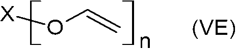
- 前記ビニルエーテル基含有架橋剤(B)が、下記式(VE-1)で表される化合物、下記式(VE-2)で表される化合物、及び下記式(VE-3)で表される化合物の少なくともいずれかである、請求項1に記載の保護膜形成用組成物。

式(VE-2)中、R2は、3価の有機基を表す。
式(VE-3)中、R3は、それぞれ独立して、2価の有機基を表す。n1は、2~6の整数を表す。) - 請求項1から7のいずれかに記載の保護膜形成用組成物から形成された保護膜。
- 請求項8に記載の保護膜を有する半導体基板。
- 請求項8に記載の保護膜を有する電子部品。
- 加工された半導体基板の製造方法であって、
請求項9に記載の半導体基板と支持基材とを、前記保護膜である異物除去用コーティング膜を介して貼り合わせて積層体を製造する第1工程と、
該積層体を加工する第2工程と、
前記異物除去用コーティング膜に光を照射する第3工程と、
該積層体から前記支持基材を剥離する第4工程と、
前記半導体基板又は前記支持基材を除去液で洗浄して、前記異物除去用コーティング膜を除去する第5工程とを含む、加工された半導体基板の製造方法。 - 前記第5工程で前記異物除去用コーティング膜とともに異物を除去する、請求項11に記載の加工された半導体基板の製造方法。
- 前記第1工程が、前記半導体基板と前記支持基材とを、前記異物除去用コーティング膜及び接着剤層を介して貼り合わせて積層体を製造する工程である、請求項11に記載の加工された半導体基板の製造方法。
- 前記第5工程で前記異物除去用コーティング膜と共に、前記接着剤層の剥離残渣である異物を除去する、請求項13に記載の半導体基板の製造法方法。
- 前記加工が、前記半導体基板と第2の半導体基板とを接続することを含む、請求項11に記載の加工された半導体基板の製造方法。
- 前記第3工程が、前記第4工程の後かつ前記第5工程の前に行われる、請求項11に記載の加工された半導体基板の製造方法。
Priority Applications (3)
| Application Number | Priority Date | Filing Date | Title |
|---|---|---|---|
| JP2025502214A JPWO2024176757A1 (ja) | 2023-02-20 | 2024-01-31 | |
| CN202480013450.6A CN120712637A (zh) | 2023-02-20 | 2024-01-31 | 保护膜形成用组合物、半导体基板及电子部件 |
| KR1020257028679A KR20250155534A (ko) | 2023-02-20 | 2024-01-31 | 보호막 형성용 조성물, 반도체 기판, 및 전자 부품 |
Applications Claiming Priority (2)
| Application Number | Priority Date | Filing Date | Title |
|---|---|---|---|
| JP2023024117 | 2023-02-20 | ||
| JP2023-024117 | 2023-02-20 |
Publications (1)
| Publication Number | Publication Date |
|---|---|
| WO2024176757A1 true WO2024176757A1 (ja) | 2024-08-29 |
Family
ID=92500794
Family Applications (1)
| Application Number | Title | Priority Date | Filing Date |
|---|---|---|---|
| PCT/JP2024/003036 Ceased WO2024176757A1 (ja) | 2023-02-20 | 2024-01-31 | 保護膜形成用組成物、半導体基板、及び電子部品 |
Country Status (5)
| Country | Link |
|---|---|
| JP (1) | JPWO2024176757A1 (ja) |
| KR (1) | KR20250155534A (ja) |
| CN (1) | CN120712637A (ja) |
| TW (1) | TW202502941A (ja) |
| WO (1) | WO2024176757A1 (ja) |
Citations (3)
| Publication number | Priority date | Publication date | Assignee | Title |
|---|---|---|---|---|
| WO1999015935A1 (en) * | 1997-09-22 | 1999-04-01 | Clariant International Ltd. | Novel process for preparing resists |
| JP2016219459A (ja) * | 2015-05-14 | 2016-12-22 | 富士フイルム株式会社 | 保護膜形成用組成物、保護膜の製造方法、保護膜の剥離方法 |
| JP2021110796A (ja) * | 2020-01-08 | 2021-08-02 | 富士フイルム株式会社 | 感光性樹脂組成物、層状膜、感光層、積層体、キット及び半導体デバイス |
Family Cites Families (2)
| Publication number | Priority date | Publication date | Assignee | Title |
|---|---|---|---|---|
| WO2017056746A1 (ja) | 2015-09-30 | 2017-04-06 | Jsr株式会社 | 半導体基板洗浄用膜形成組成物及び半導体基板の洗浄方法 |
| WO2020008965A1 (ja) | 2018-07-04 | 2020-01-09 | Jsr株式会社 | 基板処理膜形成用組成物及び基板の処理方法 |
-
2024
- 2024-01-31 JP JP2025502214A patent/JPWO2024176757A1/ja active Pending
- 2024-01-31 WO PCT/JP2024/003036 patent/WO2024176757A1/ja not_active Ceased
- 2024-01-31 KR KR1020257028679A patent/KR20250155534A/ko active Pending
- 2024-01-31 CN CN202480013450.6A patent/CN120712637A/zh active Pending
- 2024-02-16 TW TW113105533A patent/TW202502941A/zh unknown
Patent Citations (3)
| Publication number | Priority date | Publication date | Assignee | Title |
|---|---|---|---|---|
| WO1999015935A1 (en) * | 1997-09-22 | 1999-04-01 | Clariant International Ltd. | Novel process for preparing resists |
| JP2016219459A (ja) * | 2015-05-14 | 2016-12-22 | 富士フイルム株式会社 | 保護膜形成用組成物、保護膜の製造方法、保護膜の剥離方法 |
| JP2021110796A (ja) * | 2020-01-08 | 2021-08-02 | 富士フイルム株式会社 | 感光性樹脂組成物、層状膜、感光層、積層体、キット及び半導体デバイス |
Also Published As
| Publication number | Publication date |
|---|---|
| JPWO2024176757A1 (ja) | 2024-08-29 |
| TW202502941A (zh) | 2025-01-16 |
| CN120712637A (zh) | 2025-09-26 |
| KR20250155534A (ko) | 2025-10-30 |
Similar Documents
| Publication | Publication Date | Title |
|---|---|---|
| CN102981368B (zh) | 含有乙烯基醚化合物的形成防反射膜的组合物 | |
| US9790407B2 (en) | Aqueous detergent soluble coating and adhesive and methods of temporary bonding for manufacturing | |
| TW201219562A (en) | Processes and compositions for removing substances from substrates | |
| US20050263743A1 (en) | Compositions and processes for photoresist stripping and residue removal in wafer level packaging | |
| TW201042402A (en) | Compositions and methods for removing organic substances | |
| US20190016999A1 (en) | Cleaning composition | |
| EP1810323A1 (en) | Compositions and processes for photoresist stripping and residue removal in wafer level packaging | |
| DE60233897D1 (de) | N für die fortgeschrittene mikrolithographie | |
| JP7281263B2 (ja) | 樹脂組成物、感光性フィルム、支持体付き感光性フィルム、プリント配線板及び半導体装置 | |
| CN103119105A (zh) | 用于从基片去除物质的包含至少一种单酰胺和/或至少一种二酰胺的聚合物或单体组合物及其使用方法 | |
| EP3894534A1 (en) | Substrate cleaning solution and method for manufacturing device | |
| US20250361419A1 (en) | Composition for forming coating film for removing foreign matters and semiconductor substrate | |
| JP2014202849A (ja) | 感光性接着剤組成物、それを用いたパターン硬化膜の製造方法及び電子部品 | |
| TWI713753B (zh) | 層合體之製造方法、層合體,及接著劑組成物 | |
| US9018308B2 (en) | Polybenzimidazole/polyacrylate mixtures | |
| CN107526251A (zh) | 阻焊剂图案的形成方法 | |
| KR102559679B1 (ko) | 감광성 수지 조성물 | |
| KR20250155534A (ko) | 보호막 형성용 조성물, 반도체 기판, 및 전자 부품 | |
| JP2019087543A (ja) | 対象物の処理方法、洗浄剤、半導体装置およびその製造方法 | |
| KR20220044759A (ko) | 영구 접합 및 패터닝 재료 | |
| TW202219231A (zh) | 永久性黏合及圖案材料 | |
| KR20170130279A (ko) | 봉지체의 제조 방법, 및 적층체 | |
| WO2025192471A1 (ja) | 異物除去用コーティング膜形成組成物及び半導体基板 | |
| WO2025154589A1 (ja) | 異物除去用コーティング膜形成組成物及び半導体基板 | |
| WO2026014430A1 (ja) | 異物除去用コーティング膜形成組成物及び半導体基板 |
Legal Events
| Date | Code | Title | Description |
|---|---|---|---|
| 121 | Ep: the epo has been informed by wipo that ep was designated in this application |
Ref document number: 24760064 Country of ref document: EP Kind code of ref document: A1 |
|
| WWE | Wipo information: entry into national phase |
Ref document number: 2025502214 Country of ref document: JP |
|
| ENP | Entry into the national phase |
Ref document number: 1020257028679 Country of ref document: KR Free format text: ST27 STATUS EVENT CODE: A-0-1-A10-A15-NAP-PA0105 (AS PROVIDED BY THE NATIONAL OFFICE) |
|
| NENP | Non-entry into the national phase |
Ref country code: DE |
|
| WWP | Wipo information: published in national office |
Ref document number: 1020257028679 Country of ref document: KR |
|
| 122 | Ep: pct application non-entry in european phase |
Ref document number: 24760064 Country of ref document: EP Kind code of ref document: A1 |