WO2024176704A1 - 反射型マスクブランク、反射型マスク及び半導体デバイスの製造方法 - Google Patents
反射型マスクブランク、反射型マスク及び半導体デバイスの製造方法 Download PDFInfo
- Publication number
- WO2024176704A1 WO2024176704A1 PCT/JP2024/002152 JP2024002152W WO2024176704A1 WO 2024176704 A1 WO2024176704 A1 WO 2024176704A1 JP 2024002152 W JP2024002152 W JP 2024002152W WO 2024176704 A1 WO2024176704 A1 WO 2024176704A1
- Authority
- WO
- WIPO (PCT)
- Prior art keywords
- film
- thin film
- phase shift
- reflective mask
- reflectance
- Prior art date
- Legal status (The legal status is an assumption and is not a legal conclusion. Google has not performed a legal analysis and makes no representation as to the accuracy of the status listed.)
- Ceased
Links
Classifications
-
- G—PHYSICS
- G03—PHOTOGRAPHY; CINEMATOGRAPHY; ANALOGOUS TECHNIQUES USING WAVES OTHER THAN OPTICAL WAVES; ELECTROGRAPHY; HOLOGRAPHY
- G03F—PHOTOMECHANICAL PRODUCTION OF TEXTURED OR PATTERNED SURFACES, e.g. FOR PRINTING, FOR PROCESSING OF SEMICONDUCTOR DEVICES; MATERIALS THEREFOR; ORIGINALS THEREFOR; APPARATUS SPECIALLY ADAPTED THEREFOR
- G03F1/00—Originals for photomechanical production of textured or patterned surfaces, e.g., masks, photo-masks, reticles; Mask blanks or pellicles therefor; Containers specially adapted therefor; Preparation thereof
- G03F1/22—Masks or mask blanks for imaging by radiation of 100nm or shorter wavelength, e.g. X-ray masks, extreme ultraviolet [EUV] masks; Preparation thereof
- G03F1/24—Reflection masks; Preparation thereof
-
- G—PHYSICS
- G03—PHOTOGRAPHY; CINEMATOGRAPHY; ANALOGOUS TECHNIQUES USING WAVES OTHER THAN OPTICAL WAVES; ELECTROGRAPHY; HOLOGRAPHY
- G03F—PHOTOMECHANICAL PRODUCTION OF TEXTURED OR PATTERNED SURFACES, e.g. FOR PRINTING, FOR PROCESSING OF SEMICONDUCTOR DEVICES; MATERIALS THEREFOR; ORIGINALS THEREFOR; APPARATUS SPECIALLY ADAPTED THEREFOR
- G03F1/00—Originals for photomechanical production of textured or patterned surfaces, e.g., masks, photo-masks, reticles; Mask blanks or pellicles therefor; Containers specially adapted therefor; Preparation thereof
- G03F1/26—Phase shift masks [PSM]; PSM blanks; Preparation thereof
-
- G—PHYSICS
- G03—PHOTOGRAPHY; CINEMATOGRAPHY; ANALOGOUS TECHNIQUES USING WAVES OTHER THAN OPTICAL WAVES; ELECTROGRAPHY; HOLOGRAPHY
- G03F—PHOTOMECHANICAL PRODUCTION OF TEXTURED OR PATTERNED SURFACES, e.g. FOR PRINTING, FOR PROCESSING OF SEMICONDUCTOR DEVICES; MATERIALS THEREFOR; ORIGINALS THEREFOR; APPARATUS SPECIALLY ADAPTED THEREFOR
- G03F1/00—Originals for photomechanical production of textured or patterned surfaces, e.g., masks, photo-masks, reticles; Mask blanks or pellicles therefor; Containers specially adapted therefor; Preparation thereof
- G03F1/26—Phase shift masks [PSM]; PSM blanks; Preparation thereof
- G03F1/32—Attenuating PSM [att-PSM], e.g. halftone PSM or PSM having semi-transparent phase shift portion; Preparation thereof
Definitions
- the present invention relates to a reflective mask blank and a reflective mask used in the manufacture of semiconductor devices, and a method for manufacturing semiconductor devices using the reflective mask.
- EUV lithography using EUV (Extreme Ultra Violet) light, which is an extreme ultraviolet ray with a wavelength of about 13.5 nm, has been proposed.
- EUV lithography a reflective mask is used because the difference in the absorption rate of EUV light between materials is small.
- a multilayer reflective film that reflects exposure light is formed on a substrate, and a thin film (absorber film or phase shift film) that absorbs exposure light is formed in a pattern on the multilayer reflective film has been proposed.
- Light incident on a reflective mask mounted on an exposure machine (pattern transfer device) is absorbed in areas with a thin film pattern and reflected by a multilayer reflective film in areas without a thin film pattern, resulting in a light image being transferred onto a semiconductor substrate through a reflective optical system.
- the thin film is a phase shift film, part of the exposure light incident on the phase shift film pattern is reflected with a phase difference from the light reflected by the multilayer reflective film (phase shift), thereby allowing the desired contrast (resolution) to be obtained.
- Patent Document 1 describes how, in order to improve transfer resolution by applying the principles of halftone masks to EUV exposure, the material of a halftone film (phase shift film) made of a single layer is selected from a predetermined region in a diagram shown in planar coordinates with the refractive index and extinction coefficient as the coordinate axes.
- a specific material for the single layer TaMo (composition ratio 1:1) is described.
- Patent Document 2 describes that in a halftone EUV mask, in order to provide a degree of freedom in selectability of reflectance and high cleaning resistance, and to reduce the projection effect (shadowing effect), the material of the halftone film is a compound of Ta and Ru, and the composition range is specified.
- Reflective mask blanks, and reflective masks obtained by forming a transfer pattern on a reflective mask blank are manufactured through a variety of processes, including deposition of a multilayer thin film onto a substrate, formation of a resist film, pattern etching, and cleaning.
- high-level quality control is usually implemented to minimize variations in manufacturing conditions between lots.
- slight variations in manufacturing conditions or unforeseen damage that occurs during the manufacturing process can cause deviations between the actual values and the design values of the film thickness and density of the thin film (phase shift film), resulting in errors and variations in optical characteristics such as the amount of phase shift within the mask blank or mask or between individual masks.
- the present invention aims to provide a reflective mask blank and a reflective mask that can ensure high-quality and stable production by minimizing the film thickness and density dependence of the optical properties of the thin film, such as the amount of phase shift, as well as a method for manufacturing semiconductor devices using the reflective mask.
- the present invention has the following configuration.
- Configuration 1 of the present invention is a reflective mask blank having a substrate, a multilayer reflective film formed on the substrate, and a thin film formed on the multilayer reflective film, characterized in that a rate of change in reflectance of the thin film in the range of light wavelengths from 13.525 nm to 13.550 nm is not less than ⁇ 12%/nm and not more than 4%/nm.
- a second aspect of the present invention is the reflective mask blank according to the first aspect, wherein the thin film is made of a material containing at least one element selected from the group consisting of Ru, Cr, Pt, and Ta.
- a third aspect of the present invention is the reflective mask blank according to the first aspect, wherein the thin film is a phase shift film that shifts the phase of incident light.
- a fourth aspect of the present invention is the reflective mask blank according to the first aspect, wherein the thin film has a reflectance of 2% or more for EUV light.
- a fifth aspect of the present invention is the reflective mask blank according to the first aspect, wherein the rate of change in reflectance is ⁇ 10%/nm or more.
- Configuration 6 of the present invention is the reflective mask blank according to configuration 1, characterized in that the amount of change in phase shift when the thickness of the thin film varies by 1% or the amount of change in phase shift when the density of the thin film varies by 1% is 2 degrees or less.
- Configuration 7 of the present invention is the reflective mask blank according to configuration 1, characterized in that, when ⁇ max is a wavelength at which the reflectance spectrum of the thin film has a maximum reflectance in the wavelength range of 13 nm to 14 nm, and CW is an average value of two wavelengths that are closest to 13.53 nm among the wavelengths at which the reflectance is 1/2 of the maximum reflectance, the difference between ⁇ max and CW is 0.05 nm or less.
- Configuration 8 of the present invention is a reflective mask having a substrate, a multilayer reflective film formed on the substrate, and a thin film provided on the multilayer reflective film and having a transfer pattern formed thereon, wherein a rate of change in reflectance of the thin film in the range of light wavelengths from 13.525 nm to 13.550 nm is not less than ⁇ 12%/nm and not more than 4%/nm.
- a ninth aspect of the present invention is the reflective mask according to the eighth aspect, wherein the thin film is made of a material containing at least one element selected from the group consisting of Ru, Cr, Pt, and Ta.
- a tenth aspect of the present invention is the reflective mask according to the eighth aspect, wherein the thin film is a phase shift film that shifts the phase of incident light.
- An eleventh aspect of the present invention is the reflective mask according to the eighth aspect, wherein the thin film has a reflectance of 2% or more for EUV light.
- a twelfth aspect of the present invention is the reflective mask according to the eighth aspect, wherein the rate of change in reflectance is ⁇ 10%/nm or more.
- Structure 13 of the present invention is the reflective mask according to structure 8, characterized in that the amount of change in phase shift when the thickness of the thin film varies by 1% or the amount of change in phase shift when the density of the thin film varies by 1% is 2 degrees or less.
- Structure 14 of the present invention is the reflective mask according to structure 8, characterized in that, when ⁇ max is the wavelength at which the reflectance spectrum of the thin film has maximum reflectance in the wavelength range from 13 nm to 14 nm, and CW is the average value of two wavelengths that are closest to 13.53 nm among the wavelengths at which the reflectance is 1/2 of the maximum reflectance, the difference between ⁇ max and CW is 0.05 nm or less.
- Configuration 15 of the present invention is a method for manufacturing a semiconductor device, comprising exposing and transferring a transfer pattern to a transfer target on a semiconductor substrate using a reflective mask having a transfer pattern manufactured using the reflective mask blank according to any one of configurations 1 to 7.
- a sixteenth aspect of the present invention is a method for manufacturing a semiconductor device, comprising exposing and transferring the transfer pattern onto a transfer target on a semiconductor substrate using a reflective mask according to any one of the eighth to fourteenth aspects.
- the present invention it is possible to reduce the film thickness or density dependency of the optical properties (e.g., phase shift amount) of a thin film, particularly a phase shift film, formed on a reflective mask blank.
- the film thickness or density of the phase shift film varies slightly from the design value during the manufacturing process of the reflective mask blank and/or reflective mask, it is possible to stably manufacture high-quality reflective mask blanks and reflective masks having the desired optical properties (phase shift amount).
- a high-quality reflective mask having the desired optical characteristics can be used for EUV exposure, so the quality of semiconductor devices having fine and highly accurate transfer patterns can be stably guaranteed.
- FIG. 2 is a schematic cross-sectional view of a main portion for explaining the general configuration of a reflective mask blank.
- 1A to 1C are process diagrams showing, in schematic cross-sectional views of essential parts, steps for producing a reflective mask from a reflective mask blank.
- FIG. 1 is a schematic cross-sectional view of a main part for explaining the configuration of a reflective mask blank 100 of this embodiment.
- the reflective mask blank 100 includes a mask blank substrate 1 (hereinafter, simply referred to as "substrate 1"), a multilayer reflective film 2 formed on a first main surface (front surface) side and reflecting EUV light, which is exposure light, a protective film 3 provided to protect the multilayer reflective film 2 and formed of a material resistant to an etchant used in patterning a thin film (phase shift film 4) described later and a cleaning solution, and a phase shift film (sometimes referred to as an "absorbing film”) 4 as a thin film that absorbs EUV light, which are laminated in this order.
- phase shift film 4 sometimes referred to as an "absorbing film”
- a back conductive film 5 for an electrostatic chuck is formed on the second main surface (back surface) side of the substrate 1.
- the thin film may be referred to as a phase shift film, but the thin film may be a so-called binary film.
- the EUV light includes light with a wavelength of 13.5 nm, for example, light with a wavelength of 13 nm to 14 nm. In this specification, light includes not only visible light but also electromagnetic waves.
- the reflectance (absolute reflectance) of a thin film means the absolute reflectance from the surface of the thin film when the thin film is formed on the multilayer reflective film formed on the substrate, and the same applies to the relative reflectance of the thin film.
- the reflectance of a multilayer reflective film means the reflectance from the surface of the multilayer reflective film when the multilayer reflective film is formed on the substrate.
- the reflectance (absolute reflectance and relative reflectance) in this specification means a value when the angle of incidence of EUV light on the thin film or multilayer reflective film is the same as the angle of incidence of EUV light used in exposure when transferring a pattern using a reflective mask or a reflective mask manufactured from a reflective mask blank, on the irradiation target.
- the light from the EUV light source when transferring the pattern is irradiated onto the reflective mask 200 via the illumination optical system at an angle of, for example, 6° to 8° with respect to a plane perpendicular to the main surface of the reflective mask 200.
- the angle of incidence of EUV light on the thin film or multilayer reflective film is not particularly limited, but can be, for example, 6 degrees.
- “having a multilayer reflective film 2 on the main surface of the mask blank substrate 1” means that the multilayer reflective film 2 is disposed in contact with the surface of the mask blank substrate 1, and also includes the case where another film is disposed between the mask blank substrate 1 and the multilayer reflective film 2.
- “having film B on film A” means that films A and B are disposed so as to be in direct contact with each other, and also includes the case where another film is disposed between films A and B.
- film A is disposed in contact with the surface of film B means that films A and B are disposed so as to be in direct contact with each other, without another film being interposed between them.
- the substrate 1 is preferably one having a low thermal expansion coefficient within the range of 0 ⁇ 5 ppb/° C.
- materials having a low thermal expansion coefficient within this range include SiO 2 —TiO 2 glass and multi-component glass ceramics.
- the first main surface of the substrate 1 on which the transfer pattern (phase shift pattern 4a) is formed is surface-processed to have a high flatness in order to obtain at least pattern transfer accuracy and positional accuracy.
- the flatness is preferably 0.1 ⁇ m or less in a 132 mm ⁇ 132 mm area of the first main surface of the substrate 1, more preferably 0.05 ⁇ m or less, and particularly preferably 0.03 ⁇ m or less.
- the second main surface on the opposite side to the side on which the transfer pattern is formed is the surface that is electrostatically chucked when set in the exposure device.
- the flatness is preferably 0.1 ⁇ m or less, more preferably 0.05 ⁇ m or less, and particularly preferably 0.03 ⁇ m or less.
- the flatness of the second main surface side of the reflective mask blank 100 is preferably 1 ⁇ m or less in a 142 mm ⁇ 142 mm area, more preferably 0.5 ⁇ m or less, and particularly preferably 0.3 ⁇ m or less.
- flatness is a value that represents the warpage (amount of deformation) of the surface, as indicated by TIR (Total Indicated Reading). This value is the absolute value of the difference in height between the highest point on the surface of substrate 1 above the focal plane, which is determined by the least squares method with the surface of substrate 1 as the reference plane, and the lowest point on the surface of substrate 1 below the focal plane.
- the surface smoothness of the substrate 1 is high.
- the surface roughness of the first main surface of the substrate 1 on which the phase shift pattern 4a, which is the transfer pattern, is formed is preferably 0.1 nm or less in root mean square roughness (RMS).
- RMS root mean square roughness
- the substrate 1 preferably has high rigidity to prevent deformation due to film stress of the film (such as the multilayer reflective film 2) formed thereon.
- the substrate 1 it is preferable for the substrate 1 to have a high Young's modulus of 65 GPa or more.
- the multilayer reflective film 2 has a function of reflecting EUV light in the reflective mask 200, and is configured as a multilayer film in which layers made of materials with different refractive indices as main components are periodically laminated. .
- the multilayer film may be stacked in multiple periods, with a high refractive index layer/low refractive index layer stacked in this order from the substrate 1 side, as one period, or may be stacked in multiple periods, with a low refractive index layer/high refractive index layer stacked in this order from the substrate 1 side, as one period.
- the top layer of the multilayer reflective film 2 i.e., the surface layer of the multilayer reflective film 2 opposite the substrate 1
- the top layer is preferably a high refractive index layer.
- the top layer is a low refractive index layer.
- the low refractive index layer constitutes the top surface of the multilayer reflective film 2, it may be easily oxidized, which may reduce the reflectance of the reflective mask 200.
- the multilayer reflective film 2 it is preferable to further form a high refractive index layer on the uppermost low refractive index layer to form the multilayer reflective film 2.
- the uppermost layer is the high refractive index layer, so it can be left as is.
- a layer containing silicon (Si) is used as the high refractive index layer.
- the material containing Si may be a Si compound containing boron (B), carbon (C), nitrogen (N), and oxygen (O) in addition to Si.
- a layer containing Si as the high refractive index layer, a reflective mask 200 for EUV lithography with excellent reflectance of EUV light can be obtained.
- a glass substrate is preferably used as the substrate 1. Si also has excellent adhesion to the glass substrate.
- a simple metal selected from molybdenum (Mo), ruthenium (Ru), rhodium (Rh), and platinum (Pt), or an alloy thereof is used as the low refractive index layer.
- the multilayer reflective film 2 for EUV light with a wavelength of 13 nm to 14 nm a Mo/Si periodic laminate film in which Mo films and Si films are alternately laminated for about 30 to 60 periods is preferably used.
- the high refractive index layer, which is the uppermost layer of the multilayer reflective film 2 may be formed of silicon (Si).
- the reflectance of such a multilayer reflective film 2 is, for example, 65% or more for EUV light with a wavelength of 13 nm to 14 nm, and the upper limit is preferably 73%.
- the film thickness and period of each constituent layer of the multilayer reflective film 2 may be appropriately selected according to the exposure wavelength, and are selected so as to satisfy the law of Bragg reflection.
- the multilayer reflective film 2 has multiple high refractive index layers and multiple low refractive index layers, but the film thicknesses of the high refractive index layers and the low refractive index layers do not have to be the same.
- the film thickness of the Si layer on the outermost surface of the multilayer reflective film 2 can be adjusted within a range that does not reduce the reflectance.
- the film thickness of the outermost Si (high refractive index layer) can be 3 nm to 10 nm.
- the multilayer reflective film 2 can be formed by a method known in the art.
- the multilayer reflective film 2 can be formed by depositing each layer by ion beam sputtering.
- a Mo/Si periodic multilayer film for example, a Si film with a thickness of about 4 nm is first deposited on the substrate 1 using a Si target by ion beam sputtering, and then a Mo film with a thickness of about 3 nm is deposited using a Mo target. This constitutes one period, and 30 to 60 periods are stacked to form the multilayer reflective film 2 (the outermost layer is a Si layer).
- it is preferable to form the multilayer reflective film 2 by supplying krypton (Kr) ion particles from an ion source and performing ion beam sputtering.
- Kr krypton
- a protective film 3 can be formed on the multilayer reflective film 2 or in contact with the surface of the multilayer reflective film 2.
- the protective film 3 also serves to protect the multilayer reflective film 2 when correcting black defects in the phase shift pattern 4a using an electron beam (EB).
- FIG. 1 shows a case where the protective film 3 is a single layer, but it can also be a laminated structure of two or more layers.
- the protective film 3 is made of a material that is resistant to an etchant and a cleaning solution used when patterning the phase shift film 4.
- the protective film 3 By forming the protective film 3 on the multilayer reflective film 2, damage to the surface of the multilayer reflective film 2 can be suppressed when manufacturing the reflective mask 200 (EUV mask) using a substrate with a multilayer reflective film. Therefore, the reflectance characteristic of the multilayer reflective film 2 for EUV light is improved.
- protective film 3 is a single layer. If protective film 3 includes multiple layers, the properties of the material of the top layer of protective film 3 (the layer in contact with phase shift film 4) become important in relation to phase shift film 4. If phase shift film 4 includes multiple layers, the properties of the material of the bottom layer of phase shift film 4 (the layer in contact with protective film 3) become important in relation to (the top layer of) protective film 3.
- a material that is resistant to the etching gas used in the dry etching for patterning the phase shift film 4 formed on the protective film 3 can be selected as the material for the protective film 3.
- the protective film 3 can be made of, for example, a material containing Ru (ruthenium) as a main component (main component: 50 atomic % or more).
- the material containing Ru as a main component can be Ru metal alone, a Ru alloy containing Ru and one or more metals selected from Nb, Zr, Y, B, Ti, La, Mo, Co, Cr, Rh and/or Re, or a material containing nitrogen (N) and oxygen (O) in these materials.
- the protective film 14 can also have a laminated structure of three or more layers, with the bottom and top layers being layers made of a material containing Ru as a main component, and a metal other than Ru or an alloy being interposed between the bottom and top layers.
- EUV exposure can cause contamination such as the deposition of a carbon film on the mask or the growth of an oxide film. Therefore, when a reflective mask is used in the manufacture of semiconductor devices, it must be cleaned frequently to remove foreign matter and contamination from the reflective mask. For this reason, reflective masks are required to have a cleaning resistance that is orders of magnitude higher than that of transmissive masks used in optical lithography. By providing the reflective mask 200 with the protective film 3, it is possible to increase the cleaning resistance to cleaning solutions.
- the thickness of the protective film 3 is not particularly limited as long as it can perform the function of protecting the multilayer reflective film 2. From the viewpoint of the reflectance of EUV light, the thickness of the protective film 3 is preferably 1.0 nm to 8.0 nm, and more preferably 1.5 nm to 6.0 nm.
- the method for forming the protective film 3 can be any known film formation method without any particular restrictions. Specific examples include sputtering and ion beam sputtering.
- phase shift film 4 that shifts the phase of EUV light is formed as a thin film on the protective film 3.
- the phase shift film 4 may be a single layer film or a laminated film including multiple layers.
- the laminated film may include a lower layer and an upper layer formed on the lower layer.
- the lower layer may be, for example, a buffer layer.
- the lower layer may further include multiple layers. The same applies to the upper layer.
- the phase shift film 4 phase shift pattern 4a
- the EUV light is absorbed and reduced, while a part of the light is reflected at a level that does not adversely affect the pattern transfer.
- the EUV light is reflected from the multilayer reflective film 2 through the protective film 3.
- the phase shift film 4 is formed so that the reflected light from the surface of the multilayer reflective film 2 and the reflected light from the surface of the phase shift film 4 have a predetermined phase difference (also referred to as the "phase shift amount").
- a predetermined phase difference also referred to as the "phase shift amount”
- phase shift amount For example, light having a phase difference between each other within a range of 100 to 300 degrees interferes with each other at the pattern edge portion, thereby improving the image contrast of the projected optical image.
- the resolution increases and various latitudes relating to exposure, such as exposure dose latitude and focus latitude, are expanded.
- the lower limit of the phase difference of the reflected light of the phase shift film 4 relative to the reflected light from the multilayer reflective film 2 is 100 degrees or more, preferably 150 degrees or more, more preferably 180 degrees or more, and even more preferably 200 degrees or more.
- the upper limit of the phase difference of the reflected light of the phase shift film 4 relative to the reflected light from the multilayer reflective film 2 may be 310 degrees or less, preferably 300 degrees or less, more preferably 280 degrees or less, and even more preferably 250 degrees or less.
- the absolute reflectance from the surface of the phase shift film 4 (phase shift pattern 4a) to EUV light is preferably 2% or more.
- absolute reflectance means the reflected light intensity relative to the incident light intensity.
- absolute reflectance amount of light reflected from the surface of the phase shift film / amount of light incident on the surface of the phase shift film
- the relative reflectance from the surface of the phase shift film 4 is preferably 3% or more, and more preferably 4% or more. Also, the relative reflectance from the surface of the phase shift film 4 is preferably 30% or less, and more preferably 20% or less.
- the relative reflectance from the surface of the phase shift film 4 refers to the reflectance (%) of light reflected from the surface of the phase shift film 4 relative to the reflectance of light reflected from the multilayer reflective film 2 (including protective film 3) when irradiated with EUV light, assuming that the reflectance of light reflected from this multilayer reflective film 2 (including protective film 3) is 100%.
- the relative reflectance (%) of the phase shift film is the value obtained by dividing the absolute reflectance of the phase shift film 4 by the reflectance of the multilayer reflective film 2 (including protective film 3) and multiplying this value by 100.
- the phase shift film 4 formed on the multilayer reflective film 2 of the reflective mask blank 100 according to this embodiment is formed so that in its reflectance spectrum, the rate of change in (absolute) reflectance from the wavelength of EUV light of 13.525 nm to 13.550 nm is -12%/nm or more and +4%/nm or less.
- the “rate of change in reflectance” refers to the ratio of the amount of change in absolute reflectance ( R2 - R1) obtained from the reflectance at ⁇ 1 : 13.525 nm and the reflectance at ⁇ 2 : 13.550 nm, which are wavelengths in the vicinity of the central wavelength 13.53 nm of EUV light (formula (1)).
- the rate of change in reflectance is the difference obtained by subtracting the reflectance R1 at ⁇ 1 : 13.525 nm from the reflectance R2 at ⁇ 2 : 13.550 nm, divided by the difference (0.025 nm) obtained by subtracting ⁇ 1 : 13.525 nm from ⁇ 2 : 13.550 nm.
- the inventors analyzed the reflectance spectrum and optical characteristics of the phase shift film 4 under various conditions. As a result, as described above, it was found that if the rate of change in reflectance of the phase shift film 4 is at least -12%/nm and at most +4%/nm at wavelengths of at least 13.525 nm to 13.550 nm, the film thickness dependence and density dependence of the phase shift amount in the phase shift film 4 can be sufficiently suppressed to below the desired value. In addition, 13.525 nm and 13.550 nm are very close values. Therefore, in the reflectance spectrum of the phase shift film 4, the slope of the tangent at a wavelength of 13.53 nm may be at least 12%/nm and at most +4%/nm. The above wavelength of 13.53 nm corresponds to the central wavelength ⁇ c of the EUV exposure light used to form the transfer pattern of a semiconductor device.
- the thickness dependency of the phase shift film 4 is such that the amount of change in the phase shift when the thickness of the phase shift film 4 varies by 1% is 2 degrees or less.
- the density dependency of the phase shift film 4 is such that the amount of change in the phase shift when the density of the material of the phase shift film 4 varies by 1% is 2 degrees or less.
- the change in the amount of phase shift (phase shift distribution) when the thickness or density of the phase shift film 4 varies by 1% can be obtained by simulation from data such as the refractive index n, extinction coefficient k, thickness and density of the thin film.
- the difference between the wavelength ⁇ max at which the reflectance is maximum and the wavelength CW at which the half-width of the maximum reflectance is the median is 0.05 nm or less in the wavelength range of 13 nm to 14 nm in the reflectance spectrum of the phase shift film 4 for EUV light.
- the difference (distance) between the wavelength ⁇ max and CW is 0.05 nm or less.
- the reflectance spectrum refers to a spectrum in which the absolute reflectance from the surface of the thin film (phase shift film) 4 is taken as the vertical axis and the wavelength of the irradiated light (electromagnetic wave) is taken as the horizontal axis.
- etching or the like preferably dry etching is possible with chlorine (Cl)-based gas and/or fluorine (F)-based gas
- Examples of materials for the phase shift film 4 include materials containing at least one element selected from ruthenium (Ru), tantalum (Ta), chromium (Cr), rhodium (Rh), molybdenum (Mo), niobium (Nb), titanium (Ti), zirconium (Zr), yttrium (Y), silicon (Si), palladium (Pd), silver (Ag), platinum (Pt), gold (Au), iridium (Ir), tungsten (W), cobalt (Co), manganese (Mn), tin (Sn), vanadium (V), nickel (Ni), iron (Fe), hafnium (Hf), copper (Cu), tellurium (Te), zinc (Zn), magnesium (Mg), germanium (Ge), and aluminum (Al).
- the material for the phase shift film 4 may also contain at least one element selected from oxygen (O), nitrogen (N), carbon (C), and boron (B).
- the phase shift film 4 is more preferably made of a material containing at least one element selected from Ru, Cr, Pt, and Ta.
- a material containing at least one element selected from Ru, Cr, Pt, and Ta examples include Ru-based materials, RuCr-based materials, RuPt-based materials, RuTa-based materials, TaNb-based materials, IrTa-based materials, Cr-based materials, Pt-based materials, PtTa-based materials, PtCr-based materials, PtTi-based materials, PtNb-based materials, and PtMo-based materials.
- the material may further contain at least one element selected from O, N, C, and B.
- the phase shift film 4 can be formed by a known film formation method such as magnetron sputtering, such as DC sputtering and RF sputtering, or ion beam sputtering.
- the sputtering target can contain at least one of the following elements: Ru, Ta, Cr, Rh, Mo, Nb, Ti, Zr, Y, Si, Pd, Ag, Pt, Au, Ir, W, Co, Mn, Sn, V, Ni, Fe, Hf, Cu, Te, Zn, Mg, Ge, and Al.
- a back conductive film 5 for electrostatic chuck may be formed on the second main surface (back surface) side (opposite to the surface on which the multilayer reflective film 2 is formed) of the substrate 1.
- the electrical characteristics (sheet resistance) of the back conductive film 5 for electrostatic chuck is preferably 100 ⁇ / ⁇ ( ⁇ /Square) or less.
- the back conductive film 5 can be formed, for example, by magnetron sputtering or ion beam sputtering using a target of a metal or alloy such as chromium or tantalum.
- the material of the back conductive film 5 is preferably a material containing chromium (Cr) or tantalum (Ta).
- the material of the back conductive film 5 is preferably a Cr compound containing Cr and at least one selected from boron, nitrogen, oxygen, and carbon.
- Cr compounds include CrN, CrON, CrCN, CrCON, CrBN, CrBON, CrBCN, and CrBOCN.
- the material of the back conductive film 5 is preferably Ta (tantalum), an alloy containing Ta, or a Ta compound containing any of these and at least one of boron, nitrogen, oxygen, and carbon.
- Ta compounds include TaB, TaN, TaO, TaON, TaCON, TaBN, TaBO, TaBON, TaBCON, TaHf, TaHO, TaHN, TaHON, TaHON, TaHCON, TaSi, TaSiO, TaSiN, TaSiONCON, TaSi, TaSiO, TaSiN, TaSiON, and TaSiCON.
- the thickness of the back surface conductive film 5 is not particularly limited as long as it satisfies the function for use in an electrostatic chuck, but is usually 10 nm to 200 nm.
- this back surface conductive film 5 also serves to adjust the stress on the second main surface side of the mask blank 100, and is adjusted to obtain a flat reflective mask blank 100 by balancing the stress from the various films formed on the first main surface side.
- an etching mask film (not shown) can be further formed on the phase shift film 4 as necessary.
- the etching mask film is preferably formed of a material having etching selectivity with respect to the phase shift film 4. Examples of materials for the etching mask film include materials containing one or more elements selected from Cr, Ta, and Si, and materials further containing one or more elements selected from O, N, C, and B in addition to these materials.
- the etching mask film may be a single layer film or a laminated film containing multiple layers.
- the etching mask film can be formed by known methods such as DC sputtering, RF sputtering, and ion beam sputtering.
- the thickness of the etching mask film is preferably 5 nm or more from the viewpoint of ensuring its function as a hard mask.
- the thickness of the etching mask film is desirably 5 nm or more and 20 nm or less, and preferably 5 nm or more and 15 nm or less.
- the non-patterned region can be covered with a film with low reflectivity (binary film) to prevent unnecessary exposure of the transfer target (such as a resist film) on the semiconductor substrate corresponding to the non-patterned region.
- This binary film may be provided separately between the etching mask film and the thin film.
- the etching mask film may be used as the binary film.
- the reflective mask blank 100 of this embodiment can reduce the film thickness and density dependence of the phase shift amount in the phase shift film 4 compared to the conventional method. As a result, even if slight variations occur in the film thickness and density of the phase shift film 4 during the manufacturing process of the reflective mask blank 100, a high-quality reflective mask blank 100 having the desired optical characteristics can be stably manufactured.
- the reflective mask 200 has a phase shift pattern 4a formed by patterning the phase shift film 4 of the above-mentioned reflective mask blank 100.
- the phase shift pattern 4a can be formed by patterning the phase shift film 4 of the reflective mask blank 100 with a predetermined dry etching gas (e.g., a dry etching gas containing a chlorine-based gas and an oxygen gas, or a dry etching gas containing fluorine).
- a predetermined dry etching gas e.g., a dry etching gas containing a chlorine-based gas and an oxygen gas, or a dry etching gas containing fluorine.
- FIGS 2A to 2D are schematic diagrams showing an example of a method for manufacturing a reflective mask 200.
- a reflective mask blank 100 is prepared, which has a substrate 1, a multilayer reflective film 2 formed on the substrate 1, a protective film 3 formed on the multilayer reflective film 2, and a phase shift film 4 formed on the protective film 3.
- a resist film 11 is formed on the phase shift film 4 of the reflective mask blank 100 ( Figure 2A).
- the thickness of the resist film 11 is, for example, 100 nm.
- a pattern is drawn on the resist film 11 by exposure using an electron beam lithography device, and then a development and rinsing process is performed to form a resist pattern 11a ( Figure 2B). Then, using the resist pattern 11a as a mask, the phase shift film 4 is dry etched. As a result, the portion of the phase shift film 4 that is not covered by the resist pattern 11a is removed, and a phase shift pattern 4a is formed ( Figure 2C).
- the etching gas for the phase shift film 4 is appropriately selected depending on the material of the phase shift film.
- the etching gas for the phase shift film 4 may be, but is not limited to, a chlorine-based gas containing oxygen, an oxygen gas/fluorine-based gas, or a chlorine-based gas not containing oxygen gas depending on the material of the phase shift film 4 and its composition ratio.
- an etching mask film may be provided on the phase shift film 4 as necessary, and the phase shift film 4 may be dry-etched using the etching mask film pattern as a mask to form the phase shift pattern 4a.
- the resist pattern 11a is removed by ashing or using a resist stripper, and then wet cleaning is performed using an acidic or alkaline aqueous solution ( Figure 2D).
- a reflective mask 200 having the desired transfer pattern is manufactured.
- the reflective mask 200 of this embodiment can reduce the film thickness and density dependence of the phase shift amount in the phase shift pattern 4a compared to the conventional method. As a result, even if slight variations occur in the film thickness or density of the phase shift film 4 during the manufacturing process of the reflective mask blank 100 or the reflective mask 200, a high-quality reflective mask 200 having the desired optical characteristics can be stably manufactured.
- the reflective mask 200 is set in an exposure tool having an exposure light source of EUV light, and a transfer pattern is transferred to a transfer target (resist film) formed on a transfer (semiconductor) substrate, thereby manufacturing a semiconductor device.
- the semiconductor device manufacturing method of this embodiment allows a high-quality reflective mask 200 with the desired optical characteristics to be used for exposure transfer, so the quality of semiconductor devices with fine and highly accurate transfer patterns can be reliably guaranteed.
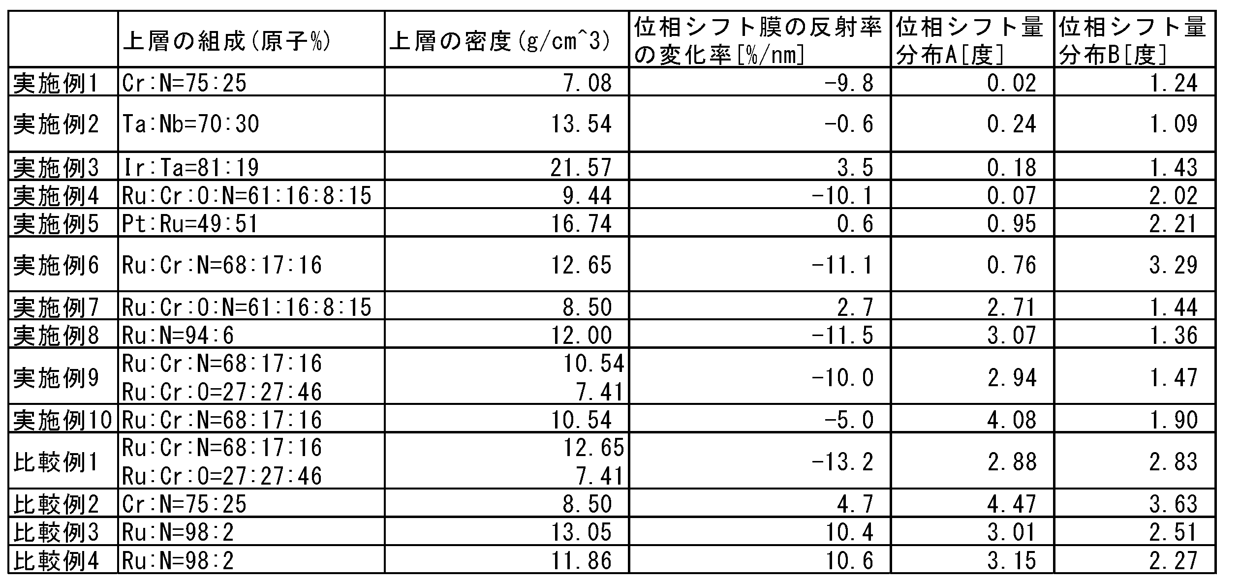
- the rate of change in reflectance of the phase shift film represents the rate of change in absolute reflectance of the thin film (phase shift film) 4 from wavelengths of 13.525 nm to 13.550 nm.
- the rate of change in reflectance of these phase shift films was calculated from the absolute reflectances measured at wavelengths of 13.525 nm and 13.550 nm.
- the reflective mask blanks of Examples 1 to 10 had a rate of change in reflectance from wavelengths of 13.525 nm to 13.550 nm of -12/nm or more and +4%/nm or less.
- none of Comparative Examples 1 to 4 satisfied this requirement.
- the rate of change in reflectance of the phase shift film may be determined from the reflectance spectrum of the thin film when EUV light with a central wavelength of about 13.5 nm is incident. Even in this case, the reflective mask blanks of Examples 1 to 10 had a rate of change in reflectance from wavelengths of 13.525 nm to 13.550 nm of -12/nm or more and +4%/nm or less, while none of Comparative Examples 1 to 4 satisfied this requirement.
- phase shift distribution A is the change in phase shift amount [degrees] when the thickness of the thin film 4 (phase shift film) changes by 1%, that is, it is an index showing the film thickness dependency of the phase shift amount.
- Phase shift distribution B is the change in phase shift amount [degrees] when the density of the thin film (phase shift film) 4 changes by 1%, that is, it is an index showing the density dependency of the phase shift amount. Note that, when the thin film (phase shift film) 4 includes a lower layer and an upper layer, the change in phase shift amount [degrees] indicates the value when the thickness or density of the upper layer changes by 1%.
- the phase shift amount distributions A and B can be obtained by simulation from the refractive index n, extinction coefficient k, film thickness, density, and the like of the thin film.
- phase shift film 4 will be simply referred to as the thin film 4.
- Example 1 A multilayer reflective film 2 was formed on the main surface of a SiO 2 -TiO 2 based glass substrate 1, and a protective film 3 made of a RuNb film was formed on the surface of the multilayer reflective film 2. Next, a lower layer made of TaBN and an upper layer made of CrN were formed on the lower layer on the protective film 3, thereby forming a thin film 4 as a phase shift film 4.
- the conditions for forming the thin film 4 in this Example 1 are shown below. Lower layer (TaBN film): TaB alloy target, Ar and N2 mixed gas atmosphere, film thickness 4 nm Upper layer (CrN film): Cr target, Ar and N2 mixed gas atmosphere, film thickness 37.1 nm
- the absolute reflectance of the thin film 4 described above at an EUV light wavelength of 13.5 nm was 2.9%.
- the density of the lower layer was 14.99 g/ cm3
- the density of the upper layer was 7.08 g/ cm3 .
- the phase shift amount of the thin film 4 formed under these conditions at a wavelength of 13.5 nm was 142 degrees.
- the rate of change in reflectance of the thin film 4 in Example 1 from wavelengths of 13.525 nm to 13.550 nm was -9.8%/nm.
- the phase shift amount distribution A of the thin film 4 at this time was 0.02 degrees
- the phase shift amount distribution B was 1.24 degrees, both of which were below the predetermined 2 degrees.
- Example 2 A multilayer reflective film 2 was formed on the main surface of a SiO 2 —TiO 2 based glass substrate 1, and a thin film 4 made of TaNb was formed on the surface of the multilayer reflective film 2.
- the conditions for forming the thin film 4 in this Example 2 are as follows. TaNb film: TaNb alloy target, Ar gas atmosphere, film thickness 39.8 nm
- the absolute reflectance of the thin film 4 made of the TaNb film at an EUV light wavelength of 13.5 nm was 9.1%.
- the density of the thin film 4 was 13.54 g/ cm3 .
- the phase shift amount of the thin film 4 formed under these conditions at a wavelength of 13.5 nm was 103 degrees.
- the rate of change in reflectance of the thin film 4 in Example 2 from wavelengths of 13.525 nm to 13.550 nm was -0.6%/nm.
- the phase shift amount distribution A of the thin film 4 at this time was 0.24 degrees
- the phase shift amount distribution B was 1.09 degrees, both of which were below the prescribed 2 degrees.
- Example 3 A multilayer reflective film 2 was formed on the main surface of a SiO 2 —TiO 2 based glass substrate 1, and a thin film 4 made of IrTa was formed on the surface of the multilayer reflective film 2.
- the conditions for forming the thin film 4 in this Example 3 are as follows. IrTa film: IrTa alloy target, Ar gas atmosphere, film thickness 25.7 nm
- the absolute reflectance of the thin film 4 made of the IrTa film at an EUV light wavelength of 13.5 nm was 6.0%.
- the density of the thin film 4 was 21.57 g/ cm3 .
- the phase shift amount of the thin film 4 formed under these conditions at an EUV light wavelength of 13.5 nm was 125 degrees.
- the rate of change in reflectance of the thin film 4 in Example 3 from wavelengths of 13.525 nm to 13.550 nm was 3.5%/nm.
- the phase shift amount distribution A of the thin film 4 at this time was 0.18 degrees
- the phase shift amount distribution B was 1.43 degrees, both of which were below the specified 2 degrees.
- Example 4 A multilayer reflective film 2 was formed on the main surface of a SiO 2 -TiO 2 based glass substrate 1, and a protective film 3 made of a RuRhCrN film was formed on the surface of the multilayer reflective film 2. Next, a lower layer made of TaON and an upper layer made of RuCrON were formed on the lower layer to form a thin film 4. The conditions for forming the thin film 4 in Example 4 are shown below. Lower layer (TaON film): Ta target, mixed gas atmosphere of Ar, O2 and N2 , film thickness 3 nm Upper layer (RuCrON film): RuCr alloy target, mixed gas atmosphere of Ar, O2 and N2 , film thickness 38.9 nm
- the absolute reflectance of the thin film 4 made of the TaON film and RuCrON film described above at an EUV light wavelength of 13.5 nm was 10.8%.
- the density of the lower layer was 9.28 g/ cm3
- the density of the upper layer was 9.44 g/ cm3 .
- the phase shift amount of the thin film 4 formed under these conditions at a wavelength of 13.5 nm was 195 degrees.
- the rate of change in reflectance of the thin film 4 in Example 4 from wavelengths of 13.525 nm to 13.550 nm was -10.1%/nm.
- the phase shift distribution A of the thin film 4 at this time was 0.07 degrees, which was less than the specified 2 degrees.
- Example 5 A multilayer reflective film 2 was formed on the main surface of a SiO 2 -TiO 2 based glass substrate 1, and a protective film 3 made of a RuRhCrN film was formed on the surface of the multilayer reflective film 2. Next, a lower layer made of CrN and an upper layer made of PtRu were formed on the lower layer to form a thin film 4. The conditions for forming the thin film 4 in Example 5 are shown below. Lower layer (CrN film): Cr target, Ar and N2 mixed gas atmosphere, film thickness 4 nm Upper layer (PtRu film): PtRu alloy target, Ar gas atmosphere, film thickness 30.2 nm
- the absolute reflectance of the thin film 4 made of the above CrN film and PtRu film at an EUV light wavelength of 13.5 nm was 3.6%.
- the density of the lower layer was 7.08 g/ cm3
- the density of the upper layer was 16.74 g/ cm3 .
- the phase shift amount of the thin film 4 formed under these conditions at a wavelength of 13.5 nm was 199 degrees.
- the rate of change in reflectance of the thin film 4 in Example 5 from wavelengths of 13.525 nm to 13.550 nm was 0.6%/nm.
- the phase shift distribution A of the thin film 4 at this time was 0.95 degrees, which was less than the specified 2 degrees.
- Example 6 A multilayer reflective film 2 was formed on the main surface of a SiO 2 -TiO 2 based glass substrate 1, and a protective film 3 made of a RuNb film was formed on the surface of the multilayer reflective film 2. Next, a lower layer made of TaBO and an upper layer made of RuCrN were formed on the lower layer to form a thin film 4. The conditions for forming the thin film 4 in Example 6 are shown below. Lower layer (TaBO film): TaB alloy target, Ar and O2 mixed gas atmosphere, film thickness 6 nm Upper layer (RuCrN film): RuCr alloy target, Ar and N2 mixed gas atmosphere, film thickness 44.5 nm
- the refractive index n and extinction coefficient k at a wavelength of 13.5 nm of the TaBO film and RuCrN film of Example 6 formed as described above were as follows, respectively.
- the absolute reflectance of the thin film 4 consisting of the TaBO film and the RuCrN film at an EUV light wavelength of 13.5 nm was 4.2%.
- the density of the lower layer was 9.00 g/ cm3
- the density of the upper layer was 12.65 g/ cm3 .
- the phase shift amount of the thin film 4 formed under these conditions at a wavelength of 13.5 nm was 298 degrees.
- the rate of change in reflectance of the thin film 4 in Example 6 from wavelengths of 13.525 nm to 13.550 nm was -11.1%/nm.
- the phase shift distribution A of the thin film 4 at this time was 0.76 degrees, which was less than the specified 2 degrees.
- Example 7 A multilayer reflective film 2 was formed on the main surface of a SiO 2 -TiO 2 based glass substrate 1, and a protective film 3 made of a RuRhCrN film was formed on the surface of the multilayer reflective film 2. Next, a lower layer made of TaON and an upper layer made of RuCrON were formed on the lower layer to form a thin film 4. The conditions for forming the thin film 4 in Example 7 are shown below. Lower layer (TaON film): Ta target, mixed gas atmosphere of Ar, O2 and N2 , film thickness 3 nm Upper layer (RuCrON film): RuCr alloy target, mixed gas atmosphere of Ar, O2 and N2 , film thickness 35.2 nm
- the absolute reflectance of the thin film 4 made of the TaON film and RuCrON film described above at an EUV light wavelength of 13.5 nm was 18.0%.
- the density of the lower layer was 9.28 g/ cm3
- the density of the upper layer was 8.50 g/ cm3 .
- the phase shift amount of the thin film 4 formed under these conditions at a wavelength of 13.5 nm was 164 degrees.
- the rate of change in reflectance of the thin film 4 in Example 7 from wavelengths of 13.525 nm to 13.550 nm was 2.7%/nm.
- the phase shift distribution B of the thin film 4 at this time was 1.44 degrees, which was less than the specified 2 degrees.
- Example 8 A multilayer reflective film 2 was formed on the main surface of a SiO 2 -TiO 2 based glass substrate 1, and a protective film 3 made of a RuRhCrN film was formed on the surface of the multilayer reflective film 2. Next, a lower layer made of TaBN and TaBO laminated in this order was formed on the protective film 3, and an upper layer made of RuN was formed on the lower layer, thereby forming a thin film 4.
- the conditions for forming the thin film 4 in Example 8 are shown below.
- the absolute reflectance of thin film 4 consisting of the above TaBN film, TaBO film and RuN film at an EUV light wavelength of 13.5 nm was 11.9%.
- the density of the TaBN film was 14.99 g/cm 3
- the density of the TaBO film was 9.00 g/cm 3
- the density of the upper layer was 12.00 g/cm 3 .
- the phase shift amount of thin film 4 formed under these conditions at a wavelength of 13.5 nm was 204 degrees.
- the rate of change in reflectance of the thin film 4 in Example 8 from wavelengths of 13.525 nm to 13.550 nm was -11.5%/nm.
- the phase shift distribution B of the thin film 4 at this time was 1.36 degrees, which was less than the specified 2 degrees.
- Example 9 A multilayer reflective film 2 was formed on the main surface of a SiO 2 -TiO 2 based glass substrate 1, and a protective film 3 made of a RuNb film was formed on the surface of the multilayer reflective film 2. Next, a lower layer made of TaBO and an upper layer made by laminating RuCrN and RuCrO in this order on the lower layer were formed on the protective film 3, thereby forming a thin film 4. The conditions for forming the thin film 4 in Example 9 are shown below.
- the absolute reflectance of thin film 4 consisting of the above TaBO film and RuCrN/RuCrO film at an EUV light wavelength of 13.5 nm was 12.5%.
- the density of the TaBO film was 9.00 g/ cm3
- the density of the RuCrN film was 10.54 g/ cm3
- the density of the RuCrO film was 7.41 g/ cm3 .
- the phase shift amount of thin film 4 formed under these conditions at a wavelength of 13.5 nm was 194 degrees.
- the rate of change in reflectance of the thin film 4 in Example 9 from wavelengths of 13.525 nm to 13.550 nm was -10.0%/nm.
- the phase shift distribution B of the thin film 4 at this time was 1.47 degrees, which was less than the prescribed 2 degrees.
- Example 10 A multilayer reflective film 2 was formed on the main surface of a SiO 2 -TiO 2 based glass substrate 1, and a protective film 3 made of a RuNb film was formed on the surface of the multilayer reflective film 2. Next, a lower layer made of TaBO and an upper layer made of RuCrN were formed on the lower layer to form a thin film 4. The conditions for forming the thin film 4 in Example 10 are shown below. Lower layer (TaBO film): TaB alloy target, Ar and O2 mixed gas atmosphere, film thickness 6 nm Upper layer (RuCrN film): RuCr alloy target, Ar and N2 mixed gas atmosphere, film thickness 38.8 nm
- the refractive index n and extinction coefficient k at a wavelength of 13.5 nm of the TaBO film and RuCrN film of Example 10 formed as described above were as follows, respectively.
- the absolute reflectance of the thin film 4 composed of the TaBO film and RuCrN film described above at an EUV light wavelength of 13.5 nm was 12.2%.
- the density of the TaBO film was 9.00 g/ cm3
- the density of the RuCrN film was 10.54 g/ cm3 .
- the phase shift amount of the thin film 4 formed under these conditions at a wavelength of 13.5 nm was 224 degrees.
- the rate of change in reflectance of the thin film 4 in Example 10 from wavelengths of 13.525 nm to 13.550 nm was -5.0%/nm.
- the phase shift distribution B of the thin film 4 at this time was 1.90 degrees, which was less than the specified 2 degrees.
- a reflective mask was manufactured from the reflective mask blanks obtained in Examples 1 to 10, and a transfer image was obtained by simulating the transfer of the resist film (transfer target) on a semiconductor device by exposure to EUV light using this reflective mask.
- the transfer pattern in this transfer image had high CD in-plane uniformity and was fine and highly accurate. From these results, it was found that when a transfer pattern is transferred to a resist film on a semiconductor device using a reflective mask obtained from the reflective mask blanks of Examples 1 to 10, the circuit pattern finally formed on the semiconductor device can be formed with high accuracy.
- Comparative Example 1 In Comparative Example 1, a multilayer reflective film was formed on the main surface of the same SiO 2 -TiO 2 glass substrate as in the Example, and a protective film made of a RuNb film was formed on the multilayer reflective film. A lower layer made of TaBO and an upper layer made of a RuCrN film and a RuCrO film were formed on the lower layer in this order to form a thin film. The conditions for forming the thin film 4 in Comparative Example 1 are shown below.
- the density of the TaBO film was 9.00 g/ cm3
- the density of the RuCrN film was 12.65 g/ cm3
- the density of the RuCrO film was 7.41 g/ cm3 .
- Phase shift amount distribution A of the thin film 4 at this time was 2.88 degrees (>2 degrees), indicating high film thickness dependency.
- Phase shift amount distribution B of the thin film 4 was 2.83 degrees (>2 degrees), indicating high density dependency as well.
- Comparative Example 2 In Comparative Example 2, a multilayer reflective film was formed on the main surface of the same SiO 2 —TiO 2 glass substrate as in the Example, and a protective film made of a RuNb film was formed on the multilayer reflective film. A thin film was formed by forming a lower layer made of TaBN on the protective film 3 and an upper layer made of CrN on the lower layer. The conditions for forming the thin film 4 in Comparative Example 2 are shown below. Lower layer (TaBN film): TaB alloy target, Ar and N2 mixed gas atmosphere, film thickness 4 nm Upper layer (CrN film): Cr target, Ar and N2 mixed gas atmosphere, film thickness 43.1 nm
- the density of the TaBN film was 14.99 g/ cm3 , and the density of the CrN film was 8.50 g/ cm3 .
- phase shift distribution A of thin film 4 in this case was 4.47 degrees (>2 degrees), indicating high film thickness dependency.
- Phase shift distribution B of thin film 4 was 3.63 degrees (>2 degrees), indicating high density dependency.
- Comparative Example 3 In Comparative Example 3, a multilayer reflective film was formed on the main surface of the same SiO 2 -TiO 2 glass substrate as in the Example, and a protective film made of a RuRhCrN film was formed on the multilayer reflective film. A lower layer made of a TaBN film and a TaBO film formed on the TaBN film, and an upper layer made of a RuN film on the lower layer were formed on the lower layer to form a thin film 4. The conditions for forming the thin film 4 in Comparative Example 3 are shown below.
- the density of the TaBN film was 14.99 g/ cm3
- the density of the TaBO film was 9.00 g/ cm3
- the density of the RuN film was 13.05 g/ cm3 .
- Phase shift amount distribution A of the thin film 4 at this time was 3.01 degrees (>2 degrees), indicating high film thickness dependency.
- Phase shift amount distribution B of the thin film 4 was 2.51 degrees (>2 degrees), indicating high density dependency as well.
- Comparative Example 4 has a film structure made of the same materials and composition as Comparative Example 3, but differs from Comparative Example 3 in the thickness of each layer constituting the lower layer and the density of the upper layer.
- the conditions for forming the thin film in Comparative Example 4 are shown below.
- the density of the TaBN film was 14.99 g/cm 3
- the density of the TaBO film was 9.00 g/cm 3
- the density of the RuN film was 11.86 g/cm 3 .
- Phase shift amount distribution A of the thin film 4 at this time was 3.15 degrees (>2 degrees), indicating high film thickness dependency.
- Phase shift amount distribution B of the thin film 4 was 2.27 degrees (>2 degrees), indicating high density dependency as well.
- Reflective masks were manufactured from the reflective mask blanks obtained in Comparative Examples 1 to 4, and the transferred images obtained by exposing and transferring the resist film (transfer target) on a semiconductor device with EUV light using these reflective masks were obtained by simulation.
- the CD in-plane uniformity of the transferred pattern in the transferred image was lower than in Examples 1 to 10, and did not have sufficient CD in-plane uniformity.
Landscapes
- Physics & Mathematics (AREA)
- General Physics & Mathematics (AREA)
- Preparing Plates And Mask In Photomechanical Process (AREA)
- Exposure Of Semiconductors, Excluding Electron Or Ion Beam Exposure (AREA)
Abstract
Description
本発明の構成1は、基板と、前記基板上に形成された多層反射膜と、前記多層反射膜上に形成された薄膜とを有する反射型マスクブランクであって、光の波長13.525nmから13.550nmにおける、前記薄膜の反射率の変化率が-12%/nm以上かつ4%/nm以下であることを特徴とする反射型マスクブランクである。
本発明の構成2は、前記薄膜が、Ru、Cr、Pt及びTaから選ばれる少なくとも1つを含む材料からなることを特徴とする、構成1に記載の反射型マスクブランクである。
本発明の構成3は、前記薄膜が、入射した光の位相をシフトさせる位相シフト膜であることを特徴とする、構成1に記載の反射型マスクブランクである。
本発明の構成4は、EUV光に対する前記薄膜の反射率が2%以上であることを特徴とする、構成1に記載の反射型マスクブランクである。
本発明の構成5は、前記反射率の変化率が-10%/nm以上であることを特徴とする、構成1に記載の反射型マスクブランクである。
本発明の構成6は、前記薄膜の膜厚が1%変動したときの位相シフト量の変化量又は前記薄膜の密度が1%変動したときの位相シフト量の変化量が2度以下であることを特徴とする、構成1に記載の反射型マスクブランクである。
本発明の構成7は、前記薄膜の反射率スペクトルの波長13nmから14nmにおいて、最大反射率となる波長をλmaxとし、前記反射率が前記最大反射率の1/2となる波長のうち最も13.53nmに近い2つの波長の平均値をCWとしたとき、λmaxとCWとの差が0.05nm以下であることを特徴とする、構成1に記載の反射型マスクブランクである。
本発明の構成8は、基板と、前記基板上に形成された多層反射膜と、前記多層反射膜上に設けられ、転写パターンが形成された薄膜とを有する反射型マスクであって、光の波長13.525nmから13.550nmにおける、前記薄膜の反射率の変化率が-12%/nm以上かつ4%/nm以下であることを特徴とする反射型マスクである。
本発明の構成9は、前記薄膜が、Ru、Cr、Pt及びTaから選ばれる少なくとも1つを含む材料からなることを特徴とする、構成8に記載の反射型マスクである。
本発明の構成10は、前記薄膜が、入射した光の位相をシフトさせる位相シフト膜であることを特徴とする、構成8に記載の反射型マスクである。
本発明の構成11は、EUV光に対する前記薄膜の反射率が2%以上であることを特徴とする、構成8に記載の反射型マスクである。
本発明の構成12は、前記反射率の変化率が-10%/nm以上であることを特徴とする、構成8に記載の反射型マスクである。
本発明の構成13は、前記薄膜の膜厚が1%変動したときの位相シフト量の変化量又は前記薄膜の密度が1%変動したときの位相シフト量の変化量が2度以下であることを特徴とする、構成8に記載の反射型マスクである。
本発明の構成14は、前記薄膜の反射率スペクトルの波長13nmから14nmにおいて、最大反射率となる波長をλmaxとし、前記反射率が前記最大反射率の1/2となる波長のうち最も13.53nmに近い2つの波長の平均値をCWとしたとき、λmaxとCWとの差が0.05nm以下であることを特徴とする、構成8に記載の反射型マスクである。
本発明の構成15は、構成1から7のいずれかに記載の反射型マスクブランクを用いて製造された、転写パターンを有する反射型マスクを用いて、半導体基板上の転写対象に前記転写パターンを露光転写することを含むことを特徴とする半導体デバイスの製造方法である。
本発明の構成16は、構成8から14のいずれかに記載の反射型マスクを用いて、半導体基板上の転写対象に前記転写パターンを露光転写することを含むことを特徴とする半導体デバイスの製造方法である。
図1は、本実施形態の反射型マスクブランク100の構成を説明するための要部断面模式図である。図1に示されるように、反射型マスクブランク100は、マスクブランク用基板1(以下、単に「基板1」という。)と、第1主面(表面)側に形成された露光光であるEUV光を反射する多層反射膜2と、当該多層反射膜2を保護するために設けられ、後述する薄膜(位相シフト膜4)をパターニングする際に使用するエッチャントや、洗浄液に対して耐性を有する材料で形成される保護膜3と、薄膜として、EUV光を吸収する位相シフト膜(「吸収膜」という場合がある。)4とを有し、これらがこの順で積層されるものである。また、基板1の第2主面(裏面)側には、静電チャック用の裏面導電膜5が形成される。本明細書において、薄膜を位相シフト膜としている場合があるが、薄膜はいわゆるバイナリ膜であってもよい。また、EUV光は、波長13.5nmの光を含み、例えば波長13nmから14nmの光である。本明細書において、光とは可視光だけでなく電磁波も含む。
基板1は、EUV光による露光時の熱による転写パターン(位相シフトパターン4a)の歪みを防止するため、0±5ppb/℃の範囲内の低熱膨張係数を有するものが好ましく用いられる。この範囲の低熱膨張係数を有する素材としては、例えば、SiO2-TiO2系ガラス、多成分系ガラスセラミックス等を用いることができる。
多層反射膜2は、反射型マスク200において、EUV光を反射する機能を有するものであり、屈折率の異なる物質を主成分とする各層が周期的に積層された多層膜の構成となっている。
後述する反射型マスク200の製造工程におけるドライエッチング及び洗浄から多層反射膜2を保護するために、多層反射膜2の上に、又は多層反射膜2の表面に接して保護膜3を形成することができる。また、電子線(EB)を用いた位相シフトパターン4aの黒欠陥修正の際の多層反射膜2の保護も兼ね備える。ここで、図1では保護膜3が1層の場合を示しているが、2層あるいは3層以上の積層構造とすることもできる。保護膜3は、位相シフト膜4をパターニングする際に使用するエッチャント、及び洗浄液に対して耐性を有する材料で形成される。多層反射膜2上に保護膜3が形成されていることにより、多層反射膜付き基板を用いて反射型マスク200(EUVマスク)を製造する際の多層反射膜2の表面へのダメージを抑制することができる。そのため、多層反射膜2のEUV光に対する反射率特性が良好となる。
本実施形態において、保護膜3の上には、薄膜として、EUV光の位相をシフトする位相シフト膜4が形成される。位相シフト膜4は、単層膜でもよく、複数の層を含む積層膜であってもよい。該積層膜は、下層および下層上に形成された上層を含むことができる。下層は、例えばバッファ層とすることができる。下層は、さらに複数の層を含んでもよい。上層も同様である。位相シフト膜4(位相シフトパターン4a)が形成されている部分では、EUV光を吸収して減光しつつパターン転写に悪影響がないレベルで一部の光を反射させる。一方、開口部(位相シフト膜4がない部分)では、EUV光が、保護膜3を介して多層反射膜2から反射する。位相シフト膜4は、多層反射膜2の表面からの反射光と位相シフト膜4の表面からの反射光とが、所定の位相差(これを「位相シフト量」ともいう。)となるように形成される。例えば互いに100~300°の範囲内の位相差を有する光同士がパターンエッジ部で干渉し合うことにより、投影光学像の像コントラストが向上する。その像コントラストの向上にともなって解像度が上がり、露光量裕度、及び焦点裕度等の露光に関する各種裕度が拡がる。
基板1の第2主面(裏面)側(多層反射膜2形成面の反対側)には、静電チャック用の裏面導電膜5が形成されてもよい。静電チャック用の裏面導電膜5の電気的特性(シート抵抗)は100Ω/□(Ω/Square)以下であることが好ましい。裏面導電膜5の形成方法は、例えばマグネトロンスパッタリング法やイオンビームスパッタリング法により、クロム及びタンタル等の金属及び合金のターゲットを使用して形成することができる。
本実施形態による反射型マスク200は、上記の反射型マスクブランク100の位相シフト膜4がパターニングされた位相シフトパターン4aを有する。位相シフトパターン4aは、反射型マスクブランク100の位相シフト膜4を、所定のドライエッチングガス(例えば、塩素系ガスと酸素ガスとを含むドライエッチングガスやフッ素を含むドライエッチングガス)によって、位相シフト膜4をパターニングすることにより形成することができる。
次に、上記の反射型マスク200を用いた半導体デバイスの製造方法を説明する。本実施形態によれば、反射型マスク200を、EUV光の露光光源を有する露光装置にセットし、被転写(半導体)基板上に形成されている転写対象(レジスト膜)に転写パターンを転写することにより、半導体デバイスを製造することができる。
位相シフト量分布A及びBは、薄膜の屈折率n、消衰係数k、膜厚及び密度などからシミュレーションにより求めることができる。
Si02-TiO2系ガラス基板1の主表面上に、多層反射膜2を形成し、多層反射膜2の表面にRuNb膜からなる保護膜3を成膜した。次に、保護膜3上に、TaBNからなる下層と、下層上にCrNからなる上層とを成膜することにより、位相シフト膜4としての薄膜4を形成した。この実施例1による薄膜4の形成条件を下記に示す。
下層(TaBN膜):TaB合金ターゲット、ArとN2の混合ガス雰囲気、膜厚4nm
上層(CrN膜):Crターゲット、ArとN2の混合ガス雰囲気、膜厚37.1nm
下層(TaBN膜):n=0.9511、k=0.0325
上層(CrN膜):n=0.9279、k=0.0384
Si02-TiO2系ガラス基板1の主表面上に、多層反射膜2を形成し、多層反射膜2の表面に、TaNbからなる薄膜4を形成した。この実施例2による薄膜4の形成条件を下記に示す。
TaNb膜:TaNb合金ターゲット、Arガス雰囲気、膜厚39.8nm
TaNb膜:n=0.9522、k=0.0244
Si02-TiO2系ガラス基板1の主表面上に、多層反射膜2を形成し、多層反射膜2の表面に、IrTaからなる薄膜4を形成した。この実施例3による薄膜4の形成条件を下記に示す。
IrTa膜:IrTa合金ターゲット、Arガス雰囲気、膜厚25.7nm
IrTa膜:n=0.9149、k=0.0430
Si02-TiO2系ガラス基板1の主表面上に、多層反射膜2を形成し、多層反射膜2の表面にRuRhCrN膜からなる保護膜3を成膜した。次に、保護膜3上に、TaONからなる下層と、下層上にRuCrONからなる上層を成膜することにより、薄膜4を形成した。この実施例4による薄膜4の形成条件を下記に示す。
下層(TaON膜):Taターゲット、Ar、O2及びN2の混合ガス雰囲気、膜厚3nm
上層(RuCrON膜):RuCr合金ターゲット、Ar、O2及びN2の混合ガス雰囲気、膜厚38.9nm
下層(TaON膜):n=0.9550,k=0.0255
上層(RuCrON膜):n=0.9091、k=0.0196
Si02-TiO2系ガラス基板1の主表面上に、多層反射膜2を形成し、多層反射膜2の表面にRuRhCrN膜からなる保護膜3を成膜した。次に、保護膜3上に、CrNからなる下層と、下層上にPtRuからなる上層を成膜することにより、薄膜4を形成した。この実施例5による薄膜4の形成条件を下記に示す。
下層(CrN膜):Crターゲット、ArとN2の混合ガス雰囲気、膜厚4nm
上層(PtRu膜):PtRu合金ターゲット、Arガス雰囲気、膜厚30.2nm
下層(CrN膜):n=0.9279,k=0.0384
上層(PtRu膜):n=0.8908、k=0.0385
Si02-TiO2系ガラス基板1の主表面上に、多層反射膜2を形成し、多層反射膜2の表面にRuNb膜からなる保護膜3を成膜した。次に、保護膜3上に、TaBOからなる下層と、下層上にRuCrNからなる上層を成膜することにより、薄膜4を形成した。この実施例6による薄膜4の形成条件を下記に示す。
下層(TaBO膜):TaB合金ターゲット、ArとO2の混合ガス雰囲気、膜厚6nm
上層(RuCrN膜):RuCr合金ターゲット、ArとN2の混合ガス雰囲気、膜厚44.5nm
下層(TaBO膜):n=0.9573,k=0.0261
上層(RuCrN膜):n=0.8803、k=0.0246
Si02-TiO2系ガラス基板1の主表面上に、多層反射膜2を形成し、多層反射膜2の表面にRuRhCrN膜からなる保護膜3を成膜した。次に、保護膜3上に、TaONからなる下層と、下層上にRuCrONからなる上層を成膜することにより、薄膜4を形成した。この実施例7による薄膜4の形成条件を下記に示す。
下層(TaON膜):Taターゲット、Ar、O2及びN2の混合ガス雰囲気、膜厚3nm
上層(RuCrON膜):RuCr合金ターゲット、Ar、O2及びN2の混合ガス雰囲気、膜厚35.2nm
下層(TaON膜):n=0.9550,k=0.0255
上層(RuCrON膜):n=0.9182、k=0.0177
Si02-TiO2系ガラス基板1の主表面上に、多層反射膜2を形成し、多層反射膜2の表面にRuRhCrN膜からなる保護膜3を成膜した。次に、保護膜3上に、TaBNと、TaBOとをこの順で積層してなる下層と、下層上にRuNからなる上層を成膜することにより、薄膜4を形成した。この実施例8による薄膜4の形成条件を下記に示す。
下層(TaBN膜):TaB合金ターゲット、ArとN2の混合ガス雰囲気、膜厚13.2nm
下層(TaBO膜):TaB合金ターゲット、ArとO2の混合ガス雰囲気、膜厚4.9nm
上層(RuN膜):Ruターゲット、ArとN2の混合ガス雰囲気、膜厚26.5nm
下層(TaBN膜):n=0.9511、k=0.0325
下層(TaBO膜):n=0.9573、k=0.0261
上層(RuN膜):n=0.8891、k=0.0170
Si02-TiO2系ガラス基板1の主表面上に、多層反射膜2を形成し、多層反射膜2の表面にRuNb膜からなる保護膜3を成膜した。次に、保護膜3上に、TaBOからなる下層と、下層上にRuCrN及びRuCrOをこの順で積層してなる上層とを成膜することにより、薄膜4を形成した。この実施例9による薄膜4の形成条件を下記に示す。
下層(TaBO膜):TaB合金ターゲット、ArとO2の混合ガス雰囲気、膜厚10.5nm
上層(RuCrN膜):RuCr合金ターゲット、ArとN2の混合ガス雰囲気、膜厚29.2nm
上層(RuCrO膜):RuCr合金ターゲット、ArとO2の混合ガス雰囲気、膜厚4nm
下層(TaBO膜):n=0.9573、k=0.0261
上層(RuCrN膜):n=0.9003、k=0.0205
上層(RuCrO膜):n=0.9213、k=0.0268
Si02-TiO2系ガラス基板1の主表面上に、多層反射膜2を形成し、多層反射膜2の表面にRuNb膜からなる保護膜3を成膜した。次に、保護膜3上に、TaBOからなる下層と、下層上にRuCrNからなる上層とを成膜することにより、薄膜4を形成した。この実施例10による薄膜4の形成条件を下記に示す。
下層(TaBO膜):TaB合金ターゲット、ArとO2の混合ガス雰囲気、膜厚6nm
上層(RuCrN膜):RuCr合金ターゲット、ArとN2の混合ガス雰囲気、膜厚38.8nm
下層(TaBO膜):n=0.9573、k=0.0261
上層(RuCrN膜):n=0.9003、k=0.0205
比較例1では、実施例と同一のSi02-TiO2系ガラス基板の主表面上に、多層反射膜を形成し、多層反射膜の上に、RuNb膜からなる保護膜を形成した。保護膜上に、TaBOからなる下層と、下層上にRuCrN膜及びRuCrO膜からなる上層とをこの順に成膜することにより、薄膜を形成した。
比較例1による薄膜4の形成条件を下記に示す。
下層(TaBO膜):TaB合金ターゲット、ArとO2の混合ガス雰囲気、膜厚10.5nm
上層(RuCrN膜):RuCr合金ターゲット、ArとN2の混合ガス雰囲気、膜厚43.5nm
上層(RuCrO膜):RuCr合金ターゲット、ArとO2の混合ガス雰囲気、膜厚4nm
比較例2では、実施例と同一のSi02-TiO2系ガラス基板の主表面上に、多層反射膜を形成し、多層反射膜の上に、RuNb膜からなる保護膜を形成した。保護膜3上に、TaBNからなる下層と、下層上にCrNからなる上層とを成膜することにより、薄膜を形成した。
比較例2による薄膜4の形成条件を下記に示す。
下層(TaBN膜):TaB合金ターゲット、ArとN2の混合ガス雰囲気、膜厚4nm
上層(CrN膜):Crターゲット、ArとN2の混合ガス雰囲気、膜厚43.1nm
比較例3では、実施例と同一のSi02-TiO2系ガラス基板の主表面上に、多層反射膜を形成し、多層反射膜の上に、RuRhCrN膜からなる保護膜を形成した。保護膜3上に、TaBN膜及びTaBN膜上に形成されたTaBO膜からなる下層と、下層上にRuN膜からなる上層とを成膜し、薄膜4を形成した。
比較例3による薄膜4の形成条件を下記に示す。
下層(TaBN膜):TaB合金ターゲット、ArとN2の混合ガス雰囲気、膜厚4nm
下層(TaBO膜):TaB合金ターゲット、ArとO2の混合ガス雰囲気、膜厚5.2nm
上層(RuN膜):Ruターゲット、ArとN2の混合ガス雰囲気、膜厚39nm
比較例4は、比較例3と同一の材料・組成からなる膜構成を有しており、比較例3とは下層を構成する各層の厚さ及び上層の密度が異なっている。
比較例4による薄膜の形成条件を下記に示す。
下層(TaBN膜):TaB合金ターゲット、ArとN2の混合ガス雰囲気、膜厚12.7nm
下層(TaBO膜):TaB合金ターゲット、ArとO2の混合ガス雰囲気、膜厚3.1nm
上層(RuN膜):Ruターゲット、ArとN2の混合ガス雰囲気、膜厚39nm
2 多層反射膜
3 保護膜
4 位相シフト膜(薄膜)
5 裏面導電膜
100 反射型マスクブランク
200 反射型マスク
Claims (16)
- 基板と、
前記基板上に形成された多層反射膜と、
前記多層反射膜上に形成された薄膜と
を有する反射型マスクブランクであって、
光の波長13.525nmから13.550nmにおける、前記薄膜の反射率の変化率が-12%/nm以上かつ4%/nm以下であることを特徴とする反射型マスクブランク。 - 前記薄膜が、Ru、Cr、Pt及びTaから選ばれる少なくとも1つを含む材料からなることを特徴とする、請求項1に記載の反射型マスクブランク。
- 前記薄膜が、入射した光の位相をシフトさせる位相シフト膜であることを特徴とする、請求項1に記載の反射型マスクブランク。
- EUV光に対する前記薄膜の反射率が2%以上であることを特徴とする、請求項1に記載の反射型マスクブランク。
- 前記反射率の変化率が-10%/nm以上であることを特徴とする、請求項1に記載の反射型マスクブランク。
- 前記薄膜の膜厚が1%変動したときの位相シフト量の変化量又は前記薄膜の密度が1%変動したときの位相シフト量の変化量が2度以下であることを特徴とする、請求項1に記載の反射型マスクブランク。
- 前記薄膜の反射率スペクトルの波長13nmから14nmにおいて、最大反射率となる波長をλmaxとし、前記反射率が前記最大反射率の1/2となる波長のうち最も13.53nmに近い2つの波長の平均値をCWとしたとき、λmaxとCWとの差が0.05nm以下であることを特徴とする、請求項1に記載の反射型マスクブランク。
- 基板と、
前記基板上に形成された多層反射膜と、
前記多層反射膜上に設けられ、転写パターンが形成された薄膜と
を有する反射型マスクであって、
光の波長13.525nmから13.550nmにおける、前記薄膜の反射率の変化率が-12%/nm以上かつ4%/nm以下であることを特徴とする反射型マスク。 - 前記薄膜が、Ru、Cr、Pt及びTaから選ばれる少なくとも1つを含む材料からなることを特徴とする、請求項8に記載の反射型マスク。
- 前記薄膜が、入射した光の位相をシフトさせる位相シフト膜であることを特徴とする、請求項8に記載の反射型マスク。
- EUV光に対する前記薄膜の反射率が2%以上であることを特徴とする、請求項8に記載の反射型マスク。
- 前記反射率の変化率が-10%/nm以上であることを特徴とする、請求項8に記載の反射型マスク。
- 前記薄膜の膜厚が1%変動したときの位相シフト量の変化量又は前記薄膜の密度が1%変動したときの位相シフト量の変化量が2度以下であることを特徴とする、請求項8に記載の反射型マスク。
- 前記薄膜の反射率スペクトルの波長13nmから14nmにおいて、最大反射率となる波長をλmaxとし、前記反射率が前記最大反射率の1/2となる波長のうち最も13.53nmに近い2つの波長の平均値をCWとしたとき、λmaxとCWとの差が0.05nm以下であることを特徴とする、請求項8に記載の反射型マスク。
- 請求項1から7のいずれかに記載の反射型マスクブランクを用いて製造された、転写パターンを有する反射型マスクを用いて、半導体基板上の転写対象に前記転写パターンを露光転写することを含むことを特徴とする半導体デバイスの製造方法。
- 請求項8から14のいずれかに記載の反射型マスクを用いて、半導体基板上の転写対象に前記転写パターンを露光転写することを含むことを特徴とする半導体デバイスの製造方法。
Priority Applications (1)
| Application Number | Priority Date | Filing Date | Title |
|---|---|---|---|
| KR1020257026079A KR20250151382A (ko) | 2023-02-22 | 2024-01-25 | 반사형 마스크 블랭크, 반사형 마스크 및 반도체 디바이스의 제조 방법 |
Applications Claiming Priority (2)
| Application Number | Priority Date | Filing Date | Title |
|---|---|---|---|
| JP2023025832A JP2024119143A (ja) | 2023-02-22 | 2023-02-22 | 反射型マスクブランク、反射型マスク及び半導体デバイスの製造方法 |
| JP2023-025832 | 2023-02-22 |
Publications (1)
| Publication Number | Publication Date |
|---|---|
| WO2024176704A1 true WO2024176704A1 (ja) | 2024-08-29 |
Family
ID=92501016
Family Applications (1)
| Application Number | Title | Priority Date | Filing Date |
|---|---|---|---|
| PCT/JP2024/002152 Ceased WO2024176704A1 (ja) | 2023-02-22 | 2024-01-25 | 反射型マスクブランク、反射型マスク及び半導体デバイスの製造方法 |
Country Status (4)
| Country | Link |
|---|---|
| JP (1) | JP2024119143A (ja) |
| KR (1) | KR20250151382A (ja) |
| TW (1) | TW202436990A (ja) |
| WO (1) | WO2024176704A1 (ja) |
Citations (4)
| Publication number | Priority date | Publication date | Assignee | Title |
|---|---|---|---|---|
| JP2018146945A (ja) * | 2017-03-03 | 2018-09-20 | Hoya株式会社 | 反射型マスクブランク、反射型マスク及び半導体装置の製造方法 |
| JP2021128247A (ja) * | 2020-02-13 | 2021-09-02 | Hoya株式会社 | 反射型マスクブランク、反射型マスク、導電膜付き基板、及び半導体装置の製造方法 |
| JP2022129534A (ja) * | 2021-02-25 | 2022-09-06 | Hoya株式会社 | マスクブランク、反射型マスク、および半導体デバイスの製造方法 |
| WO2022249863A1 (ja) * | 2021-05-27 | 2022-12-01 | Hoya株式会社 | マスクブランク、反射型マスク及び半導体デバイスの製造方法 |
Family Cites Families (2)
| Publication number | Priority date | Publication date | Assignee | Title |
|---|---|---|---|---|
| JP2006228766A (ja) | 2005-02-15 | 2006-08-31 | Toppan Printing Co Ltd | 極端紫外線露光用マスク、マスクブランク、及び露光方法 |
| JP5233321B2 (ja) | 2008-02-27 | 2013-07-10 | 凸版印刷株式会社 | 極端紫外線露光用マスクブランク、極端紫外線露光用マスク、極端紫外線露光用マスクの製造方法及び極端紫外線露光用マスクを用いたパターン転写方法 |
-
2023
- 2023-02-22 JP JP2023025832A patent/JP2024119143A/ja active Pending
-
2024
- 2024-01-25 WO PCT/JP2024/002152 patent/WO2024176704A1/ja not_active Ceased
- 2024-01-25 KR KR1020257026079A patent/KR20250151382A/ko active Pending
- 2024-02-05 TW TW113104395A patent/TW202436990A/zh unknown
Patent Citations (4)
| Publication number | Priority date | Publication date | Assignee | Title |
|---|---|---|---|---|
| JP2018146945A (ja) * | 2017-03-03 | 2018-09-20 | Hoya株式会社 | 反射型マスクブランク、反射型マスク及び半導体装置の製造方法 |
| JP2021128247A (ja) * | 2020-02-13 | 2021-09-02 | Hoya株式会社 | 反射型マスクブランク、反射型マスク、導電膜付き基板、及び半導体装置の製造方法 |
| JP2022129534A (ja) * | 2021-02-25 | 2022-09-06 | Hoya株式会社 | マスクブランク、反射型マスク、および半導体デバイスの製造方法 |
| WO2022249863A1 (ja) * | 2021-05-27 | 2022-12-01 | Hoya株式会社 | マスクブランク、反射型マスク及び半導体デバイスの製造方法 |
Also Published As
| Publication number | Publication date |
|---|---|
| JP2024119143A (ja) | 2024-09-03 |
| TW202436990A (zh) | 2024-09-16 |
| KR20250151382A (ko) | 2025-10-21 |
Similar Documents
| Publication | Publication Date | Title |
|---|---|---|
| US12111566B2 (en) | Reflective mask blank, reflective mask and manufacturing method thereof, and semiconductor device manufacturing method | |
| JP7502510B2 (ja) | 反射型マスクブランク、反射型マスク、及び半導体装置の製造方法 | |
| KR102906466B1 (ko) | 반사형 마스크 블랭크, 반사형 마스크, 그리고 반사형 마스크 및 반도체 장치의 제조 방법 | |
| KR102938891B1 (ko) | 반사형 마스크 블랭크 및 반사형 마스크, 그리고 반도체 장치의 제조 방법 | |
| JP7676624B2 (ja) | 反射型マスクブランク、反射型マスク、導電膜付き基板、及び半導体装置の製造方法 | |
| US20230418148A1 (en) | Multilayer reflective film-equipped substrate, reflective mask blank, reflective mask, and method for producing semiconductor device | |
| JP2007109964A (ja) | 多層反射膜付き基板、その製造方法、反射型マスクブランクおよび反射型マスク | |
| JP7743590B2 (ja) | 反射型マスクブランク、反射型マスク、反射型マスクの製造方法、及び半導体装置の製造方法 | |
| US20240411220A1 (en) | Multilayer reflective film-attached substrate, reflective mask blank, reflective mask, and method for producing semiconductor device | |
| US20240231216A1 (en) | Mask blank, reflective mask, and method for producing semiconductor devices | |
| US20230314928A1 (en) | Multilayer reflective film-equipped substrate, reflective mask blank, reflective mask manufacturing method, and semiconductor device manufacturing method | |
| TW202240279A (zh) | 光罩基底、反射型光罩、及半導體裝置之製造方法 | |
| JP7826305B2 (ja) | マスクブランク、反射型マスク及び半導体デバイスの製造方法 | |
| JP2024134733A (ja) | 反射型マスクブランク、反射型マスクの製造方法、反射型マスク、および半導体装置の製造方法 | |
| KR20250093487A (ko) | 반사형 마스크 블랭크 및 반사형 마스크, 그리고 반사형 마스크 및 반도체 장치의 제조 방법 | |
| WO2024176704A1 (ja) | 反射型マスクブランク、反射型マスク及び半導体デバイスの製造方法 | |
| WO2025089390A1 (ja) | 反射型マスクブランク、反射型マスク、及び半導体装置の製造方法 | |
| JP2025074011A (ja) | 反射型マスクブランク、反射型マスク、及び半導体装置の製造方法 | |
| WO2022203024A1 (ja) | 反射型マスクブランク、反射型マスク、反射型マスクの製造方法及び半導体装置の製造方法 | |
| TW202443289A (zh) | 反射型遮罩基底及反射型遮罩、以及反射型遮罩及半導體裝置之製造方法 |
Legal Events
| Date | Code | Title | Description |
|---|---|---|---|
| 121 | Ep: the epo has been informed by wipo that ep was designated in this application |
Ref document number: 24760011 Country of ref document: EP Kind code of ref document: A1 |
|
| ENP | Entry into the national phase |
Ref document number: 1020257026079 Country of ref document: KR Free format text: ST27 STATUS EVENT CODE: A-0-1-A10-A15-NAP-PA0105 (AS PROVIDED BY THE NATIONAL OFFICE) |
|
| NENP | Non-entry into the national phase |
Ref country code: DE |
|
| WWP | Wipo information: published in national office |
Ref document number: 1020257026079 Country of ref document: KR |
|
| 122 | Ep: pct application non-entry in european phase |
Ref document number: 24760011 Country of ref document: EP Kind code of ref document: A1 |