WO2024176373A1 - 電力変換ユニット - Google Patents
電力変換ユニット Download PDFInfo
- Publication number
- WO2024176373A1 WO2024176373A1 PCT/JP2023/006390 JP2023006390W WO2024176373A1 WO 2024176373 A1 WO2024176373 A1 WO 2024176373A1 JP 2023006390 W JP2023006390 W JP 2023006390W WO 2024176373 A1 WO2024176373 A1 WO 2024176373A1
- Authority
- WO
- WIPO (PCT)
- Prior art keywords
- explosion
- proof plate
- unit
- power conversion
- housing
- Prior art date
- Legal status (The legal status is an assumption and is not a legal conclusion. Google has not performed a legal analysis and makes no representation as to the accuracy of the status listed.)
- Ceased
Links
Images




Classifications
-
- H—ELECTRICITY
- H02—GENERATION; CONVERSION OR DISTRIBUTION OF ELECTRIC POWER
- H02M—APPARATUS FOR CONVERSION BETWEEN AC AND AC, BETWEEN AC AND DC, OR BETWEEN DC AND DC, AND FOR USE WITH MAINS OR SIMILAR POWER SUPPLY SYSTEMS; CONVERSION OF DC OR AC INPUT POWER INTO SURGE OUTPUT POWER; CONTROL OR REGULATION THEREOF
- H02M7/00—Conversion of AC power input into DC power output; Conversion of DC power input into AC power output
- H02M7/42—Conversion of DC power input into AC power output without possibility of reversal
- H02M7/44—Conversion of DC power input into AC power output without possibility of reversal by static converters
- H02M7/48—Conversion of DC power input into AC power output without possibility of reversal by static converters using discharge tubes with control electrode or semiconductor devices with control electrode
Definitions
- An embodiment of the present invention relates to a power conversion unit.
- the power conversion unit has a shelf provided in the housing and units stored on the shelf.
- the power conversion unit has a DC fuse to prevent short circuits and explosions. If a short circuit occurs in a power conversion unit, it could affect other healthy units.
- Each unit has an explosion-proof mechanism.
- the explosion-proof mechanism has a cover that seals the unit.
- the unit has a cooling mechanism for cooling the items inside.
- the cooling mechanism can be an air-cooling mechanism or a water-cooling mechanism. If the unit is sealed, heat may build up inside the unit, reducing the cooling efficiency.
- large-capacity power conversion units do not include DC fuses in order to reduce costs and size. Without DC fuses, if a short circuit occurred, it could affect other healthy units.
- the problem that this invention aims to solve is to provide a power conversion unit that can improve explosion-proof performance.
- the power conversion unit of the embodiment includes a housing, a first element, a second element, and an explosion-proof plate.
- the first element is disposed inside the housing.
- the second element is disposed inside the housing horizontally adjacent to the first element.
- the explosion-proof plate covers the first element and the second element when viewed from above the housing.
- the explosion-proof plate is a laminated conductor connected to the first element and the second element.
- FIG. 2 is a perspective view showing the configuration of a power conversion unit according to the first embodiment.
- FIG. 2 is a perspective view showing a configuration of a power control unit in the power conversion unit according to the first embodiment.
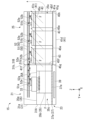
- FIG. 2 is a cross-sectional view showing a configuration of a power control unit in the power conversion unit of the first embodiment.
- FIG. 4 is a cross-sectional view showing a flow of cooling air in the power conversion unit of the first embodiment.
- FIG. 13 is a perspective view showing a configuration of a power control unit in a power conversion unit according to a second embodiment.
- FIG. 11 is a cross-sectional view showing a configuration of a power control unit in a power conversion unit according to a second embodiment.
- FIG. 13 is a perspective view showing a configuration of a power control unit in a power conversion unit according to a third embodiment.
- FIG. 13 is a cross-sectional view showing a configuration of a power control unit in a power conversion unit according to a fourth embodiment.
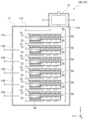
- FIG. 13 is a top view showing a unit configuration of the power conversion unit according to the fourth embodiment.
- FIG. 13 is a cross-sectional view showing a configuration of a power control unit in a power conversion unit according to a fifth embodiment.
- First Embodiment 1 is a perspective view showing a power conversion unit according to the present embodiment, in which reference numeral 10 denotes a power conversion unit.
- the X-axis, Y-axis, and Z-axis directions which are mutually orthogonal in three-dimensional space, are parallel to each other.
- the X-axis direction is parallel to the left-right direction of the power conversion unit 10.
- the Y-axis direction is parallel to the front-rear direction of the power conversion unit 10.
- the Z-axis direction is parallel to the up-down direction of the power conversion unit 10.
- the power conversion unit 10 is, for example, a panel provided in electrical equipment.
- the panel is a switchboard, distribution board, control panel, etc. that constitutes a power supply device, a motor drive device, etc.
- the power conversion unit 10 includes various circuit components such as semiconductor elements, conductors, fuses, capacitors, transformers, switches, circuit breakers, and measuring instruments.
- the power conversion unit 10 includes an operation unit 10a and a power control unit 10b.
- the operation unit 10a accepts input operations by an operator related to the operation of the power control unit 10b.
- the operation unit 10a outputs a signal that instructs the operation of the power control unit 10b in response to the input operations by the operator.
- the operation unit 10a for example, includes an input device such as an operation button and a display such as a liquid crystal display.
- the power control unit 10 b includes, for example, a housing 11 , a plurality of fans (fluid machinery) 13 , and a plurality of power control units (units) 15 .
- An upper portion 11a of the housing 11 in the Z-axis direction supports a plurality of fans 13.
- An exhaust port 11A (see FIG. 3) formed in the upper portion 11a faces and communicates with each of the fans 13, for example, along the Z-axis direction.
- a plurality of intake ports 11B formed in a front portion 11b of the housing 11 in the Y-axis direction faces, for example, an appropriate power control unit 15 along the Y-axis direction.
- Each intake port 11B is, for example, a rectangular opening.
- the housing 11 supports a number of power control units 15 disposed therein.
- the multiple fans 13 are, for example, two fans 13. Each fan 13 draws air from outside the housing 11 into the housing 11 through each intake port 11B in the front part 11b of the housing 11. Each fan 13 exhausts air from inside the housing 11 to the outside through an exhaust port 11A in the top part 11a of the housing 11. Each fan 13 cools the multiple power control units 15 with cooling air F formed by the air flowing inside the housing 11.
- the plurality of power control units 15 is, for example, 12 power control units 15.
- the plurality of power control units 15 are arranged inside the housing 11, for example, in six rows in the Z-axis direction and two rows in the X-axis direction.
- each other than the power control units 15 in the top two rows is arranged, for example, along the Y-axis direction, facing each of the intake ports 11B of the housing 11.
- Fig. 2 is a perspective view showing the configuration of the power control unit 15 in the power conversion unit 10 of this embodiment.
- Fig. 3 is a cross-sectional view showing the configuration of the power control unit 15 of this embodiment and the flow of heat and cooling air F.
- Each power control unit 15 includes, for example, an element unit 21 , a driving unit 23 , and a capacitor unit 25 . As shown in FIGS. 2 and 3, the element unit 21 and the drive unit 23 are arranged so as to be stacked along the Z-axis direction, for example.
- the element unit 21 comprises a first unit housing 31, a plurality of semiconductor elements (first elements) 33, and a heat sink (heat dissipation member) 35.
- the first unit housing 31 supports the plurality of semiconductor elements 33 and the heat sink 35 internally.
- a front opening 31A and a rear opening 31B are formed in the front part 31a and rear part 31b in the Y-axis direction of the first unit housing 31, which face and communicate with the heat sink 35 along the Y-axis direction, for example.
- the multiple semiconductor elements 33 are, for example, multiple switching elements and rectifying elements that form a bridge circuit by being bridge-connected.
- the switching elements are transistors such as IGBTs (Insulated Gate Bipolar Transistors) or MOSFETs (Metal Oxide Semiconductor Field Effect Transistors).
- the rectifying elements are diodes connected in parallel to each transistor.
- the multiple semiconductor elements 33 are arranged on the element placement surface 35A of the heat sink 35.
- the element placement surface 35A of the heat sink 35 is, for example, the upper end surface of the upper portion 35a in the Z-axis direction of the heat sink 35.
- the multiple semiconductor elements 33 are arranged, for example, in a row on the element placement surface 35A along the X-axis direction.
- the outer shape of the heat sink 35 is, for example, a rectangular parallelepiped.
- the length of the heat sink 35 along the Y-axis direction is formed to be, for example, a predetermined length longer than the length in the Y-axis direction of each semiconductor element 33 arranged on the element arrangement surface 35A.
- the predetermined length is, for example, approximately the length required to fix each semiconductor element 33 to the element arrangement surface 35A.
- the heat sink 35 includes a plurality of fin members 35b.
- the outer shape of each fin member 35b is, for example, a plate shape parallel to the YZ plane.
- the plurality of fin members 35b extend downward in the Z-axis direction from the upper portion 35a and contact a partition member 37a of the drive unit 23, which will be described later.
- the plurality of fin members 35b are arranged side by side at predetermined intervals along the X-axis direction.
- the multiple fin members 35b of the heat sink 35 form a flow path 35c for air to flow inside the housing 11.
- the flow direction of air in the heat sink 35 is set parallel to the YZ plane by the multiple fin members 35b.
- the drive unit 23 includes a second unit housing 37 and a substrate 39.
- the second unit housing 37 supports the substrate 39 disposed therein.
- the second unit housing 37 includes a partition member 37a.
- the partition member 37a separates the interior of the second unit housing 37, in which the substrate 39 is disposed, from the air flow path 35c formed by the heat sink 35.
- the partition member 37a has an outer shape, for example, a plate shape parallel to the XY plane.
- the partition member 37a prevents the air (cooling air) F flowing through the flow path 35c in the heat sink 35 from flowing into the inside of the second unit housing 37.
- the substrate 39 includes, for example, a drive substrate that drives and controls the switching elements of the multiple semiconductor elements 33 .
- the capacitor unit 25 is disposed adjacent to the element unit 21 and the drive unit 23 along the Y-axis direction while being separated from the element unit 21 and the drive unit 23, for example. 2 and 3, the capacitor unit 25 includes a third unit housing (support member) 41 and a plurality of capacitors (capacitors: second elements) 43.
- the third unit housing 41 supports the plurality of capacitors 43 arranged therein.
- the third unit housing 41 includes, for example, a left side portion 41a and a right side portion 41b in the X-axis direction, an upper portion 41c and a lower portion 41d in the Z-axis direction, and a support member 41e between the upper portion 41c and the lower portion 41d.
- the outer shape of each of the left side portion 41a and the right side portion 41b is, for example, a plate shape parallel to the YZ plane.
- Each of the left side portion 41a and the right side portion 41b may be formed with a plurality of side openings through which air (cooling air) F passes.
- Each side opening is, for example, a circular opening penetrating the left side portion 41a and the right side portion 41b.
- each of the upper portion 41c, lower portion 41d, and support member 41e is, for example, a plate-like shape parallel to the XY plane.
- the upper portion 41c has a plurality of insertion holes 45b into which a plurality of capacitors 43 are inserted.
- Each upper opening 45c is, for example, a circular opening that penetrates the upper portion 41c.
- the upper portion 41c has a plurality of upper openings 45c through which air (cooling air) F passes.
- the lower portion 41d may be formed with a plurality of lower openings for passing air (cooling air) F.
- Each lower opening is, for example, a penetrating opening having a rounded rectangular shape.
- a support member 41e on which the plurality of capacitors 43 are arranged is formed with a plurality of support portion openings (through holes) 45e for passing air (cooling air) F.
- Each support portion opening 45e is, for example, a circular through opening.
- Each opening 45f is, for example, a rectangular opening.
- an opening 45g is formed in the front portion 41f in the Y-axis direction, through which air (cooling air) F passes.
- the opening 45g is, for example, a trapezoidal opening.
- a rear portion 41g in the Y-axis direction is formed with a plurality of openings 45h for allowing air (cooling air) F to pass through.
- the plurality of openings 45h are, for example, circular through-holes.
- Each capacitor 43 includes, for example, a capacitor that smoothes out voltage fluctuations that occur with the on/off switching operation of a switching element among the multiple semiconductor elements 33 .
- the first unit housing 31, the second unit housing 37 and the third unit housing 41 may be configured as an integrated unit.
- the power control unit 15 has its upper surface covered by an explosion-proof plate 50.
- the power control unit 15 has its upper surface closed by an explosion-proof plate 50.
- the explosion-proof plate 50 is a conductor.
- the explosion-proof plate 50 can be a copper plate.
- the explosion-proof plate 50 covers at least the semiconductor elements 33 and the capacitors 43.
- the explosion-proof plate 50 covers the semiconductor elements 33 and the capacitors 43 to the extent that they are not visible when viewed from above.
- the explosion-proof plate 50 covers the element unit 21 and the capacitor unit 25.
- the explosion-proof plate 50 continuously covers the element unit 21 and the capacitor unit 25.
- the explosion-proof plate 50 blocks the upper surface of the power control unit 15. Blocking means that even if an unpredictable arc flash or the like occurs in the power control unit 15, the high-temperature gas and pressure wave associated with this are not released to the other power control units 15. Even if an unpredictable arc flash or the like occurs in the power control unit 15, the explosion-proof plate 50 does not allow the high-temperature gas and pressure wave associated with this to be released to the other power control units 15.
- the explosion-proof plate 50 has a rectangular outline that matches the outline of the power control unit 15 when viewed from above.
- the explosion-proof plate 50 has a rectangular outline that is slightly smaller than the outline of the power control unit 15 when viewed from above.
- the explosion-proof plate 50 has a predetermined thickness dimension necessary for blocking. Also, as a part of the circuit that converts a large amount of power in the power control unit 15, the explosion-proof plate 50 has a predetermined thickness dimension necessary.
- the explosion-proof plate 50 has a configuration that allows it to be closed off from the first unit housing 31 and the third unit housing 41 at both ends in the Y direction.
- the explosion-proof plate 50 has a configuration that allows it to be closed off from the first unit housing 31 and the third unit housing 41 at both ends in the X direction.
- the explosion-proof plate 50 has its end in the X direction spaced apart from the left side portion 41a and the right side portion 41b.
- the distance between the explosion-proof plate 50 and the left side portion 41a is a distance that allows insulation. This insulation distance is set based on the rated voltage of the power control unit 15, etc.
- the distance between the explosion-proof plate 50 and the right side portion 41b is a distance that allows insulation. This insulation distance is set based on the rated voltage of the power control unit 15, etc.
- the explosion-proof plate 50 may be connected to the left side portion 41a and the right side portion 41b in the X direction. In this case, the explosion-proof plate 50 and the left side portion 41a are connected by an insulator. The explosion-proof plate 50 and the right side portion 41b are connected by an insulator. The explosion-proof plate 50 is supported by the first unit housing 31 and the third unit housing 41. In the capacitor unit 25, a flow passage 25c is formed between the explosion-proof plate 50 and the third unit housing 41. The explosion-proof plate 50 is spaced apart from the semiconductor element 33 and the capacitor 43 in the Z direction.
- the explosion-proof plate 50 is connected to each of the semiconductor elements 33 and the capacitors 43.
- the explosion-proof plate 50 also serves as a PN conductor that constitutes a circuit together with the semiconductor elements 33 and the capacitors 43.
- the explosion-proof plate 50 is made up of multiple laminated conductor plates.
- the explosion-proof plate 50 is made up of, for example, a laminated conductor plate (laminated conductor) 51 and a laminated conductor plate (laminated conductor) 52.
- the conductor plates 51 and 52 can be copper plates.
- the conductor plates 51 and 52 can be copper plates with a thickness of 1 mm or more.
- the conductor plates 51 and 52 can be copper plates with a thickness of about 2 mm, or 2 mm ⁇ 0.5 mm. Both the conductor plates 51 and 52 extend along the X-Y plane.
- the conductor plate 51 and the conductor plate 52 may have substantially the same contour shape when viewed from above.
- the conductor plate 51 and the conductor plate 52 may have different contour shapes when viewed from above.
- the conductor plate 51 is disposed, for example, above the conductor plate 52 in the Z direction.
- the conductive plate 51 and the conductive plate 52 are spaced apart in the Z direction. There is a distance in the Z direction between the conductive plate 51 and the conductive plate 52.
- a spacer can be disposed in the gap in the Z direction between the conductive plate 51 and the conductive plate 52.
- the spacer is an insulator.
- the conductive plate 51 and the conductive plate 52 are connected to different terminals of the plurality of semiconductor elements 33 and the plurality of capacitors 43, respectively.
- the conductor plate 51 is connected to the semiconductor element 33 via a connection portion (spacer) 51a.
- the connection portion 51a also serves as a spacer between the conductor plate 51 and the semiconductor element 33.
- the conductor plate 51 and the connection portion 51a are fixed by bolting.
- the connection portion 51a is disposed on the upper surface of the semiconductor element 33.
- the connection portion 51a may be integral with the terminal of the semiconductor element 33.
- the connection portion 51a is made of a conductive conductor.
- the connection portion 51a is not connected to the conductor plate 52.
- the connection portion 51a passes through a through hole (opening) 52e formed in the conductor plate 52. Air (cooling air) F can pass through the through hole 52e.
- the through hole 52e is covered by the conductor plate 51 when viewed from above.
- the conductor plate 51 is located above the through hole 52e in the Z direction.
- the conductor plate 51 is connected to the capacitor 43 via a connection portion (spacer) 51b.
- the connection portion 51b also serves as a spacer between the conductor plate 51 and the capacitor 43.
- the conductor plate 51 and the connection portion 51b are fixed by bolting.
- the connection portion 51b is disposed on the upper surface of the capacitor 43.
- the connection portion 51b may be integral with the terminal of the capacitor 43.
- the connection portion 51b is made of a conductive conductor.
- the connection portion 51b is not connected to the conductor plate 52.
- the connection portion 51b passes through a through hole 52e formed in the conductor plate 52. Air (cooling air) F can pass through the through hole 52e.
- the through hole 52e is covered by the conductor plate 51 when viewed from above.
- the conductor plate 51 is located above the through hole 52e in the Z direction.
- the conductive plate 52 is connected to the semiconductor element 33 via a connection portion (spacer) 52a.
- the connection portion 52a also serves as a spacer between the conductive plate 52 and the semiconductor element 33.
- the conductive plate 52 and the connection portion 52a are fixed by bolting.
- the connection portion 52a is disposed on the upper surface of the semiconductor element 33.
- the connection portion 52a may be integral with the terminal of the semiconductor element 33.
- the connection portion 52a is made of a conductive conductor.
- the conductive plate 52 is connected to the capacitor 43 via a connection portion (spacer) 52b.
- the connection portion 52b also serves as a spacer between the conductive plate 52 and the capacitor 43.
- the conductive plate 52 and the connection portion 52b are fixed by bolting.
- the connection portion 52b is disposed on the upper surface of the capacitor 43.
- the connection portion 52b may be integral with the terminal of the capacitor 43.
- the connection portion 52b is made of a conductive conductor.
- the conductive plate 52 is spaced apart from the semiconductor element 33 and the capacitor 43 in the Z direction.
- a spacer may be placed between the conductive plate 52 and the semiconductor element 33.
- the spacer is an insulating material with high thermal conductivity.
- FIG. 4 is a cross-sectional view showing the flow of cooling air F in the power conversion unit 10 of the present embodiment.
- the power conversion unit 10 is cooled by driving a plurality of fans 13.
- the fans 13 draw air from outside the housing 11 into the housing 11 through the plurality of air intakes 11B.
- the air that passes through the inside of the housing 11 is exhausted to the outside of the housing 11 through the exhaust ports 11A and the fans 13.
- the air passing through the inside of the housing 11 acts as cooling air F in a flow path from the air intakes 11B to the exhaust ports 11A, thereby cooling the plurality of power control units 15.
- the cooling air F is sucked into the housing 11 from each intake port 11B.
- the cooling air F flows along the Y-axis direction toward the element unit 21 and the drive unit 23 of each power control unit 15.
- the cooling air F reaches each power control unit 15.
- the lower surface of the semiconductor element 33 contacts the heat sink 35. As shown in Fig. 3, heat is conducted from the semiconductor element 33 to the heat sink 35. The semiconductor element 33 is cooled. The upper surface of the semiconductor element 33 is connected to the explosion-proof plate 50 via the connection parts 51a and 52a. Heat is conducted from the semiconductor element 33 to the explosion-proof plate 50 via the connection parts 51a and 52a. The semiconductor element 33 is cooled.
- the upper surface of the semiconductor element 33 faces the lower surface of the explosion-proof plate 50.
- the upper surface of the semiconductor element 33 faces the lower surface of the conductive plate 52. Heat is radiated from the semiconductor element 33 to the explosion-proof plate 50.
- the semiconductor element 33 is cooled. In element unit 21, heat transferred from semiconductor element 33 to explosion-proof plate 50 moves toward capacitor unit 25 on which cooling air F is blowing, as will be described later.
- the cooling air F flows from the front opening 31A of the first unit housing 31 of the element unit 21 toward the heat sink 35, as shown in FIGS.
- the cooling air F passes through a flow path 35c formed by the heat sink 35.
- the cooling air F flows between the multiple fin members 35b arranged side by side at intervals.
- the cooling air F cools the fin members 35b.
- the cooling air F cools the heat sink 35.
- the multiple semiconductor elements 33 are cooled by heat dissipation from the heat sink 35.
- the cooling air F passes through the heat sink 35 and the rear opening 31B of the first unit housing 31.
- the cooling air F flows inside the third unit housing 41 of the capacitor unit 25.
- the cooling air F flows between the upper portion 41c and the support member 41e inside the third unit housing 41.
- the cooling air F flows between the multiple capacitors 43.
- the cooling air F cools each of the capacitors 43.
- the cooling air F passes through the inside of the third unit housing 41.
- the cooling air F flows toward each exhaust port 11A and each fan 13.
- the cooling air F is exhausted to the outside of the housing 11.
- capacitor 43 is cooled by cooling air F as shown in FIG.
- Capacitor 43 is connected at its upper surface to explosion-proof plate 50 via connection parts 51b and 52b. Heat is conducted from capacitor 43 to explosion-proof plate 50 via connection parts 51b and 52b.
- Capacitor 43 is cooled.
- the upper surface of the capacitor 43 faces the lower surface of the explosion-proof plate 50.
- the upper surface of the capacitor 43 faces the lower surface of the conductive plate 52. Heat is radiated from the capacitor 43 to the explosion-proof plate 50.
- the semiconductor element 33 is cooled.
- cooling air F flows along the lower surface of explosion-proof plate 50. Explosion-proof plate 50 is cooled by cooling air F. As explosion-proof plate 50 is cooled, capacitor 43 is cooled. In capacitor unit 25, cooling air F passes through through hole 52e of conductive plate 52. As a result, cooling air F passes between conductive plates 51 and 52. Conductive plates 51 and 52 are cooled by cooling air F.
- the cooling air F does not directly hit the explosion-proof plate 50.
- the explosion-proof plate 50 is cooled by the cooling air F in the capacitor unit 25.
- the explosion-proof plate 50 conducts heat from the element unit 21 to the capacitor unit 25.
- the explosion-proof plate 50 conducts heat from the element unit 21 to the capacitor unit 25, which is cooled by the cooling air F.
- the explosion-proof plate 50 can cool the element unit 21. By cooling the explosion-proof plate 50, the semiconductor element 33 and the capacitor 43 are cooled.
- cooling air F passes through a pair of openings 45f, opening 45g, and multiple openings 45h in the Y-axis direction.
- cooling air F passes through multiple side openings and multiple upper openings 45c in each of the X-axis and Z-axis directions.
- Cooling air F passes through multiple lower openings 45d and multiple support openings 45e.
- cooling air F passes through the through hole 52e of the conductor plate 52.
- the multiple capacitor units 25 arranged in the Z-axis direction function as a so-called wind tunnel for the cooling air F passing through the inside along the X-axis, Y-axis, and Z-axis directions.
- the power conversion unit 10 of this embodiment is provided with an explosion-proof plate 50 that covers the entire top surface of the power control unit 15, thereby providing a power conversion unit 10 that has excellent cooling while also being explosion-proof.
- the entire top surface of the power control unit 15 is covered by the explosion-proof plate 50, which prevents broken items from scattering and the spread of damage.
- the explosion-proof plate 50 is a laminated conductor that also serves as a PN conductor, and is made of a material (copper) with excellent electrical and thermal conductivity, which prevents heat from building up inside the power control unit 15 while maintaining low inductance. Furthermore, the power conversion unit 10 allows the number of parts in the power control unit 15 to be reduced.
- the power conversion unit 10 is configured so that the entire top surface of the power control unit 15 is covered by the explosion-proof plate 50, which increases the heat dissipation area and improves the cooling efficiency of the semiconductor element 33 and the capacitor 43 compared to a configuration without the explosion-proof plate 50.
- the semiconductor element 33 is primarily cooled by the heat sink 35.
- the heat generated by the semiconductor element 33 is transferred to the explosion-proof plate 50, which is a conductor, and the temperature of the explosion-proof plate 50 is raised by the heat, thereby further cooling the semiconductor element 33 and improving the cooling efficiency.
- multiple semiconductor elements 33 are arranged in a row along a direction perpendicular to the flow direction of the cooling air F. Moreover, all of the semiconductor elements 33 are connected to the explosion-proof plate 50. The upper surfaces of all of the semiconductor elements 33 face the explosion-proof plate 50. This improves the cooling efficiency by the explosion-proof plate 50 in addition to the heat sink 35. For example, compared to a case where multiple semiconductor elements 33 are arranged in multiple rows along the flow direction of the cooling air F, each semiconductor element 33 can be actively cooled, and since cooling can be performed by the explosion-proof plate 50, the length of the heat sink 35 in the flow direction of the cooling air F can be reduced.
- the power conversion unit 10 is designed so that the cooling air F hits the explosion-proof plate 50 on the capacitor unit 25 side, which is the downwind side of the cooling air F, so that heat can be conducted and pulled from the upwind side to the downwind side by the thermal conduction of the explosion-proof plate 50, which is a conductor, and dissipated from the explosion-proof plate 50 in the capacitor unit 25. Since the cooling air F hits the explosion-proof plate 50 in the capacitor unit 25, the explosion-proof plate 50 can also contribute to cooling the semiconductor element 33.
- the power conversion unit 10 can prevent the semiconductor element 33 on the upstream side from thermally acting on the capacitor 43 on the downstream side.
- the power conversion unit 10 can prevent the flow path of the cooling air F from becoming longer by improving the cooling efficiency with the explosion-proof plate 50.
- the explosion-proof plate 50 improves the cooling efficiency of the semiconductor element 33, thereby making it possible to prevent the flow path in the heat sink 35 from becoming longer. By preventing the flow path in the heat sink 35 from becoming longer, it is possible to prevent an increase in the temperature gradient of the heat sink 35.
- the power conversion unit 10 includes a heat sink 35 that is arranged upstream in the flow direction of the cooling air F. This allows the multiple semiconductor elements 33 arranged on the heat sink 35 to be actively cooled. Moreover, the semiconductor elements 33 can be cooled by an explosion-proof plate 50 in addition to the heat sink 35. For example, the multiple semiconductor elements 33 can be cooled more efficiently than when a semiconductor element 33 that generates a relatively large amount of heat is arranged downstream in the flow direction of the cooling air F compared to other circuit elements.
- the power conversion unit 10 includes a third unit housing 41 with multiple upper openings, as well as an explosion-proof plate 50. This allows the cooling air F to pass through the inside of the third unit housing 41 along the explosion-proof plate 50. By making the inside of the multiple third unit housings 41 and the explosion-proof plate 50 function as a wind tunnel, it is possible to suppress an increase in pressure loss inside the housing 11.
- the power conversion unit 10 can prevent the need to provide a separate ventilation path for the cooling air F inside the housing 11.
- the power conversion unit 10 can prevent the housing 11 from becoming large. By reducing the pressure loss inside the housing 11, the cooling capacity of the cooling air F inside the housing 11 can be improved and the internal capacity of the housing 11 can be increased. By having the cooling air F flow along the explosion-proof plate 50, the cooling capacity can be improved and the internal capacity of the housing 11 can be increased. By increasing the cooling capacity of the cooling air F, the increase in power consumption of each fan 13 can be suppressed and each fan 13 can be made smaller.
- the power conversion unit 10 includes a partition member 37a that separates the inside of the second unit housing 37 from the air flow path 35c formed by the heat sink 35. This makes it possible to prevent the exhaust heat of the heat sink 35 from thermally acting on the substrate 39 inside the second unit housing 37.
- the explosion-proof plate 50 that conducts heat from the element unit 21 to the capacitor unit 25 can increase the cooling efficiency of the element unit 21.
- the explosion-proof plate 50 improves the cooling efficiency of the element unit 21, and by separating the element unit 21 and the drive unit 23 from the capacitor unit 25, the ease of maintenance can be improved.
- the element unit 21, the drive unit 23, and the capacitor unit 25 may be separated from each other, or may be integrally formed in an appropriate combination.
- Fig. 5 is a perspective view showing the configuration of the power control unit 15 in the power conversion unit 10 of this embodiment.
- Fig. 6 is a cross-sectional view showing the configuration of the power control unit 15 of this embodiment.
- the insulating reinforcement portion 55 is provided to increase the strength of the explosion-proof plate 50. Specifically, the insulating reinforcement portion 55 prevents the explosion-proof plate 50 from being turned over and deformed by an upward blast from below at the four corners of the explosion-proof plate 50.
- the insulating reinforcement portion 55 is attached to the upper surface of the explosion-proof plate 50.
- the insulating reinforcement portion 55 contacts the upper surface of the explosion-proof plate 50.
- the insulating reinforcement portion 55 is attached to at least the four corners of the explosion-proof plate 50.
- the insulating reinforcement part 55 is made of an insulating material.
- the insulating reinforcement part 55 is made of a material that can provide the strength necessary to maintain the strength of the four corners so that they do not curl up when the force applied from below by the explosion-proof plate 50 is applied.
- the insulating reinforcement part 55 is made of Dallas epoxy resin, for example.
- the insulating reinforcement part 55 has a thickness and shape that can maintain the strength necessary to prevent the four corners from curling up when the force applied from below by the explosion-proof plate 50 is applied.
- the insulating reinforcement portion 55 has a rod insulating reinforcement portion 55a and a rod insulating reinforcement portion 55b.
- the rod insulation reinforcement part 55a connects two of the four corners of the explosion-proof plate 50 that are located on the same side in the Y direction.
- the rod insulation reinforcement part 55a is arranged along the side extending in the X direction of the rectangular outline of the explosion-proof plate 50 when viewed from above.
- the rod insulation reinforcement part 55a is arranged along the end of the explosion-proof plate 50 in the Y direction.
- the rod insulation reinforcement part 55a is arranged at the end of the element unit 21 of the rectangular outline of the explosion-proof plate 50 when viewed from above.
- the rod insulating reinforcement part 55a is fixed to the upper surface of the explosion-proof plate 50.
- the rod insulating reinforcement part 55a may be screwed to the explosion-proof plate 50.
- the ends of the rod insulation reinforcement part 55a in the X direction are closer to the left side part 41a and the right side part 41b than the explosion-proof plate 50.
- the ends of the rod insulation reinforcement part 55a in the X direction are connected to the left side part 41a and the right side part 41b.
- the ends of the rod insulation reinforcement part 55a in the X direction are fixed to the left side part 41a and the right side part 41b.
- the ends of the rod insulation reinforcement part 55a in the X direction may be screwed to the left side part 41a and the right side part 41b.
- the rod insulation reinforcement portion 55b connects two of the four corners of the explosion-proof plate 50 that are located on the same side in the Y direction.
- the rod insulation reinforcement portion 55b is arranged along the side extending in the X direction of the rectangular outline of the explosion-proof plate 50 when viewed from above.
- the rod insulation reinforcement portion 55b is arranged along the end of the explosion-proof plate 50 in the Y direction.
- the rod insulation reinforcement portion 55b is arranged at the end of the rectangular outline of the explosion-proof plate 50 at the capacitor unit 25.
- the rod insulating reinforcement part 55b is fixed to the upper surface of the explosion-proof plate 50.
- the rod insulating reinforcement part 55b may be screwed to the explosion-proof plate 50.
- the ends of the rod insulation reinforcement part 55b in the X direction are closer to the left side part 41a and the right side part 41b than the explosion-proof plate 50.
- the ends of the rod insulation reinforcement part 55b in the X direction are connected to the left side part 41a and the right side part 41b.
- the ends of the rod insulation reinforcement part 55b in the X direction are fixed to the left side part 41a and the right side part 41b.
- the ends of the rod insulation reinforcement part 55b in the X direction may be screwed to the left side part 41a and the right side part 41b.
- the insulating reinforcement portion 55 has a rod-shaped insulating reinforcement portion 55a and a rod-shaped insulating reinforcement portion 55b that face each other in the Y direction.
- the rod-shaped insulating reinforcement portion 55a and the rod-shaped insulating reinforcement portion 55b are arranged parallel to each other.
- the rod-shaped insulating reinforcement portion 55a and the rod-shaped insulating reinforcement portion 55b have approximately the same thickness.
- the insulating reinforcing portion 55 is fixed to the first unit housing 31 and the third unit housing 41. In this way, the explosion-proof plate 50 is fixed to the first unit housing 31 and the third unit housing 41.
- the power conversion unit 10 in this embodiment is configured with an insulating reinforcement section 55 on the explosion-proof plate 50 that covers the entire upper surface of the power control unit 15, which prevents broken items from scattering and further prevents damage from spreading. Since the insulating reinforcement section 55 is made of a material with excellent insulation properties for the explosion-proof plate 50, which is a laminated conductor, there is no need to consider electrical effects on the power control unit 15. Since the insulating reinforcement section 55 is made of a material with excellent insulation properties, it can be tightly attached to the explosion-proof plate 50, which is a laminated conductor. The insulating reinforcement section 55 can suppress deformation of the explosion-proof plate 50 due to damage.
- the insulating reinforcing portion 55 is made of a material having excellent insulating properties, so that it does not affect the performance of preventing heat buildup within the power control unit 15.
- the insulating reinforcing portion 55 is made of a material having excellent strength, so that the explosion-proof property can be further improved. Furthermore, by fixing the insulating reinforcement portion 55 to the first unit housing 31 and the third unit housing 41, the first unit housing 31 and the third unit housing 41 can be reinforced, thereby improving the strength of the power control unit 15.
- the rod insulation reinforcement portion 55a and the rod insulation reinforcement portion 55b are configured to extend over the entire length in the X direction in the contour shape of the explosion-proof plate 50, but are not limited to this configuration.
- the rod insulation reinforcement portion 55a and the rod insulation reinforcement portion 55b can also be configured to each extend a length of about 1/4 to 1/3 of the entire length in the X direction, including the corners, in the contour shape of the explosion-proof plate 50.
- FIG. 7 is a perspective view showing the configuration of the power control unit 15 in the power conversion unit 10 of the present embodiment. This embodiment differs from the above-described second embodiment in terms of the insulating reinforcing portion 55 .
- the insulating reinforcement portion 55 has a rod insulating reinforcement portion 55c and a rod insulating reinforcement portion 55d.
- the rod insulation reinforcement portion 55c connects two of the four corners of the explosion-proof plate 50 that are located on the same side in the X direction.
- the rod insulation reinforcement portion 55c is arranged along the side extending in the Y direction of the rectangular outline of the explosion-proof plate 50 when viewed from above.
- the rod insulation reinforcement portion 55c is arranged along the end of the explosion-proof plate 50 in the X direction.
- the rod insulation reinforcement portion 55c is arranged at the end of the rectangular outline of the explosion-proof plate 50 when viewed from above that extends from the element unit 21 to the capacitor unit 25.
- the rod insulating reinforcement part 55c is fixed to the upper surface of the explosion-proof plate 50.
- the rod insulating reinforcement part 55c may be screwed to the explosion-proof plate 50.
- the X-direction end of the rod insulating reinforcement part 55c is closer to the left side part 41a than the explosion-proof plate 50.
- the X-direction end of the rod insulating reinforcement part 55c protrudes beyond the outline of the explosion-proof plate 50.
- the X-direction end of the rod insulating reinforcement part 55c is connected to the left side part 41a.
- the X-direction end of the rod insulating reinforcement part 55c is fixed to the left side part 41a.
- the X-direction end of the rod insulating reinforcement part 55c may be screwed to the left side part 41a.
- the rod insulating reinforcement portion 55c is fixed to the first unit housing 31 and the third unit housing 41 over its entire length in the Y direction.
- the rod insulation reinforcement portion 55d connects two of the four corners of the explosion-proof plate 50 that are located on the same side in the X direction.
- the rod insulation reinforcement portion 55d is arranged along the side extending in the Y direction of the rectangular outline of the explosion-proof plate 50 when viewed from above.
- the rod insulation reinforcement portion 55d is arranged along the end of the explosion-proof plate 50 in the X direction.
- the rod insulation reinforcement portion 55d is arranged at the end of the rectangular outline of the explosion-proof plate 50 that extends from the element unit 21 to the capacitor unit 25.
- the rod insulating reinforcement part 55d is fixed to the upper surface of the explosion-proof plate 50.
- the rod insulating reinforcement part 55d may be screwed to the explosion-proof plate 50.
- the rod insulating reinforcement part 55b is closer to the right side part 41b at both ends in the X direction than the explosion-proof plate 50.
- the rod insulating reinforcement part 55d has an end in the X direction connected to the right side part 41b.
- the rod insulating reinforcement part 55d has an end in the X direction fixed to the right side part 41b.
- the rod insulating reinforcement part 55d may have an end in the X direction screwed to the right side part 41b.
- the rod insulating reinforcement portion 55d is fixed to the first unit housing 31 and the third unit housing 41 over its entire length in the Y direction.
- the rod insulating reinforcement portion 55c and the rod insulating reinforcement portion 55d face each other in the X direction.
- the rod insulating reinforcement portion 55c and the rod insulating reinforcement portion 55d are arranged parallel to each other.
- the rod insulating reinforcement portion 55c and the rod insulating reinforcement portion 55d have approximately the same thickness.
- the insulating reinforcing portion 55 is fixed to the first unit housing 31 and the third unit housing 41. In this way, the explosion-proof plate 50 is fixed to the first unit housing 31 and the third unit housing 41.
- the explosion-proof plate 50 can be more firmly fixed to the first unit housing 31 and the third unit housing 41.
- the insulating reinforcement portion 55 is fixed to the first unit housing 31 and the third unit housing 41 over its entire length in the Y direction, thereby eliminating gaps and further improving the explosion-proof performance.
- This embodiment also provides the same effects as the above-mentioned embodiment.
- the rod insulation reinforcement portion 55c and the rod insulation reinforcement portion 55d are configured to extend over the entire length in the Y direction in the contour shape of the explosion-proof plate 50, but are not limited to this configuration.
- the rod insulation reinforcement portion 55a and the rod insulation reinforcement portion 55b can also be configured to each extend a length of about 1/4 to 1/3, including the corners, of the entire length in the Y direction in the contour shape of the explosion-proof plate 50.
- Fig. 8 is a cross-sectional view showing the configuration of the power control unit 15 in the power conversion unit 10 of this embodiment.
- Fig. 9 is a schematic top view showing the configuration of the power control unit 15. This embodiment differs from the above-described first embodiment in terms of the through-hole (opening) 51e.
- the explosion-proof plate 50 has through holes 51e formed in the upper conductor plate 51. Air (cooling air) F can pass through the through holes (openings) 51e.
- the through holes 51e overlap the conductor plate 52 when viewed from above.
- the conductor plate 52 is located below the through holes 51e in the Z direction.
- the through holes 51e are arranged at positions corresponding to the respective through holes 52e. Specifically, the through holes 51e are arranged at positions downstream of the through holes 52e along the flow direction of the cooling air F.
- through hole 51e is positioned so as to overlap connection portion 52a when viewed from above.
- Through hole 51e is positioned so as to overlap connection portion 52b when viewed from above.
- the position of through hole 51e is not limited to this position as long as it is downstream of through hole 52e.
- the cooling air F that passes through the through-hole 52e passes further through the through-hole 51e.
- the cooling air F flows along both sides of the lower conductor plate 52.
- the cooling air F flows along the lower surface of the upper conductor plate 51.
- This embodiment also provides the same effects as the above-mentioned embodiment.
- FIG. 10 is a cross-sectional view showing the configuration of the power control unit 15 in the power conversion unit 10 of the present embodiment. This embodiment differs from the first to fourth embodiments described above in terms of the insulating and heat-transfer portion 57 .
- the insulating heat transfer portion 57 is disposed between the conductor plate 51 and the conductor plate 52.
- the insulating heat transfer portion 57 is in close contact with the conductor plate 51 and the conductor plate 52, respectively.
- the insulating heat transfer portion 57 fills the entire area between the conductor plate 51 and the conductor plate 52.
- the insulating heat transfer portion 57 may also fill the through hole 52e.
- the insulating heat transfer section 57 is made of a high-strength material.
- the insulating heat transfer section 57 is made of a material that has insulating properties.
- the insulating heat transfer section 57 is made of a material that has high thermal conductivity.
- the material of the insulating heat transfer section 57 can be selected as appropriate.
- the insulating heat transfer section 57 can be made of the same material as the insulating reinforcement section 55.
- the insulating and heat-transferring portion 57 can have the same contour shape as the explosion-proof plate 50 when viewed from above.
- the insulating heat transfer part 57 may have a contour shape that protrudes in the X direction from the contour shape of the explosion-proof plate 50 when viewed from above.
- the X direction end of the insulating heat transfer part 57 may be fixed to the first unit housing 31 and the third unit housing 41, similar to the insulating reinforcement part 55.
- the insulating heat transfer section 57 is fixed to the first unit housing 31 and the third unit housing 41 at its end in the X direction, so that the explosion-proof plate 50 can be more firmly fixed to the first unit housing 31 and the third unit housing 41.
- the X-direction end of the insulating heat transfer section 57 can be fixed to the first unit housing 31 and the third unit housing 41 over its entire length in the Y direction.
- the explosion-proof plate 50 can be more firmly fixed to the first unit housing 31 and the third unit housing 41.
- the insulating and heat-transferring section 57 is fixed to the first unit housing 31 and the third unit housing 41 over its entire length in the Y direction, thereby eliminating gaps and further improving the explosion-proof performance.
- Heat is conducted from the upper conductive plate 51 to the lower conductive plate 52 by the insulating heat transfer part 57. Heat is conducted from the lower conductive plate 52 to the upper conductive plate 51 by the insulating heat transfer part 57. Moreover, heat conduction between the conductive plates 51 and 52 is facilitated over the entire area of the explosion-proof plate 50. Heat dissipation is further promoted by the thermal conduction of the insulating heat transfer part 57. As a result, when the temperature of the conductor plate 51 is high, the heat can be conducted to the conductor plate 52 which is actively cooled by the cooling air F hitting it and flowing along it, thereby improving the cooling efficiency.
- the heat transferred from the semiconductor element 33 to the explosion-proof plate 50 can be transferred to the conductor plate 52, which is located in the capacitor unit 25 and has high cooling efficiency, and can be cooled efficiently.
- This embodiment also provides the same effects as the above-mentioned embodiment.
- the insulating heat transfer portion 57 is configured to fill the entire area of the explosion-proof plate 50, but is not limited to this configuration.
- the insulating heat transfer portion 57 may be configured such that a plurality of members equivalent to the rod insulating reinforcement portion 55a extending in the X direction are arranged between the conductor plate 51 and the conductor plate 52 at intervals in the Y direction.
- the insulating heat transfer portion 57 can be configured such that a plurality of members equivalent to the rod insulating reinforcement portion 55c extending in the Y direction are arranged between the conductive plates 51 and 52 and spaced apart in the X direction.
- the contour shape of the explosion-proof plate 50 may be configured so that each of the corners extends to a length of about 1/4 to 1/3 of the total length in the X direction.
- the insulating heat transfer section 57 can be configured such that a plurality of members equivalent to the rod insulating reinforcement section 55c extending in the Y direction are arranged between the conductor plates 51 and 52, spaced apart in the X direction, and the insulating heat transfer section 57 has a through hole 51e arranged at a position downstream of the through hole 52e along the flow direction of the cooling air F.
- the explosion-proof plate 50 can enhance explosion-proofing and improve cooling performance.
Landscapes
- Engineering & Computer Science (AREA)
- Power Engineering (AREA)
- Inverter Devices (AREA)
Abstract
電力変換ユニットは、筐体と、第1素子と、第2素子と、防爆板と、を備える。第1素子は、筐体の内部に配置される。第2素子は、筐体の内部に第1素子に水平方向に隣接して配置される。防爆板は、筐体の上面視して第1素子と第2素子とを覆う。防爆板は、第1素子および第2素子に接続される積層導体である。
Description
本発明の実施形態は、電力変換ユニットに関する。
電力変換ユニットは、筐体に設けた棚と、棚上に収納されたユニットと、を有する。電力変換ユニットは、短絡防止、防爆のため、直流ヒューズを有する。電力変換ユニットは、ユニット等で短絡が発生した場合、他の健全ユニットへ影響を及ぼす可能性があった。各ユニットは、防爆機構を有する。一例としては、防爆機構が、ユニットを密閉するカバーを有する。
ユニットは、内部の用品を冷却する冷却機構を有する。冷却機構には、風冷機構、水冷機構がある。ユニットを密閉すると、ユニット内に熱がこもり、冷却効率が低下する可能性があった。
また、大容量の電力変換ユニットは、コスト削減、小型化から直流ヒューズをなくしている。直流ヒューズがないと、短絡が発生した場合、他の健全ユニットへ影響が及ぶ可能性があった。
ユニットは、内部の用品を冷却する冷却機構を有する。冷却機構には、風冷機構、水冷機構がある。ユニットを密閉すると、ユニット内に熱がこもり、冷却効率が低下する可能性があった。
また、大容量の電力変換ユニットは、コスト削減、小型化から直流ヒューズをなくしている。直流ヒューズがないと、短絡が発生した場合、他の健全ユニットへ影響が及ぶ可能性があった。
本発明が解決しようとする課題は、防爆性能を向上させることができる電力変換ユニットを提供することである。
実施形態の電力変換ユニットは、筐体と、第1素子と、第2素子と、防爆板と、を備える。第1素子は、筐体の内部に配置される。第2素子は、筐体の内部に第1素子に水平方向に隣接して配置される。防爆板は、筐体の上面視して第1素子と第2素子とを覆う。防爆板は、第1素子および第2素子に接続される積層導体である。
以下、第1実施形態に係る電力変換ユニットを、図面に基づいて説明する。
(第1の実施形態)
図1は、本実施形態における電力変換ユニットを示す斜視図である。図において、符号10は、電力変換ユニットである。
図1は、本実施形態における電力変換ユニットを示す斜視図である。図において、符号10は、電力変換ユニットである。
以下、3次元空間で互いに直交するX軸、Y軸及びZ軸の各軸方向は、各軸に平行な方向である。例えば図1に示すように、X軸方向は電力変換ユニット10の左右方向に平行である。Y軸方向は電力変換ユニット10の前後方向に平行である。Z軸方向は電力変換ユニット10の上下方向に平行である。
本実施形態に係る電力変換ユニット10は、例えば、電気設備等に備えられる盤である。盤は、電源装置及びモータ駆動装置等を構成する配電盤、分電盤及び制御盤等である。電力変換ユニット10は、例えば、半導体素子、導体、ヒューズ、キャパシタ(コンデンサ)、トランス、開閉器、遮断器及び計測機器等の各種の回路構成要素を備える。
電力変換ユニット10は、図1に示すように、操作部10a及び電力制御部10bを備える。操作部10aは、例えば、電力制御部10bの動作に関する操作者の入力操作を受け付ける。操作部10aは、操作者の入力操作に応じて電力制御部10bの動作を指示する信号を出力する。操作部10aは、例えば、操作ボタン等の入力機器及び液晶ディスプレイ等の表示器を備える。
電力制御部10bは、例えば、筐体11と、複数のファン(流体機械)13と、複数の電力制御ユニット(ユニット)15と、を備える。
筐体11のZ軸方向での上部11aは、複数のファン13を支持する。上部11aに形成された排気口11A(図3参照)は、例えばZ軸方向に沿って各ファン13に臨んで通じている。筐体11のY軸方向での前部11bに形成された複数の吸気口11Bは、例えばY軸方向に沿って適宜の電力制御ユニット15に対向して臨んでいる。各吸気口11Bは、例えば矩形の開口である。
筐体11は、内部に配置される複数の電力制御ユニット15を支持する。
筐体11のZ軸方向での上部11aは、複数のファン13を支持する。上部11aに形成された排気口11A(図3参照)は、例えばZ軸方向に沿って各ファン13に臨んで通じている。筐体11のY軸方向での前部11bに形成された複数の吸気口11Bは、例えばY軸方向に沿って適宜の電力制御ユニット15に対向して臨んでいる。各吸気口11Bは、例えば矩形の開口である。
筐体11は、内部に配置される複数の電力制御ユニット15を支持する。
複数のファン13は、例えば2つのファン13である。各ファン13は、筐体11の前部11bの各吸気口11Bから筐体11の外部の空気を内部に吸入する。各ファン13は、筐体11の上部11aの排気口11Aから筐体11の内部の空気を外部に排出する。各ファン13は、筐体11の内部を流れる空気により形成される冷却風Fによって複数の電力制御ユニット15を冷却する。
複数の電力制御ユニット15は、例えば12個の電力制御ユニット15である。複数の電力制御ユニット15は、例えばZ軸方向に6段及びX軸方向に2列に並んで筐体11の内部に配置されている。複数の電力制御ユニット15のうち、最上段の2列の電力制御ユニット15以外の各々は、例えばY軸方向に沿って筐体11の各吸気口11Bに対向して臨むように配置されている。
図2は、本実施形態の電力変換ユニット10での電力制御ユニット15の構成を示す斜視図である。図3は、本実施形態の電力制御ユニット15の構成および熱と冷却風Fとの流れを示す断面図である。
各電力制御ユニット15は、例えば、素子ユニット21と、駆動ユニット23と、キャパシタユニット25と、を備える。
素子ユニット21と駆動ユニット23とは、図2,図3に示すように、例えばZ軸方向に沿って積層されるように配置されている。
各電力制御ユニット15は、例えば、素子ユニット21と、駆動ユニット23と、キャパシタユニット25と、を備える。
素子ユニット21と駆動ユニット23とは、図2,図3に示すように、例えばZ軸方向に沿って積層されるように配置されている。
素子ユニット21は、第1ユニット筐体31と、複数の半導体素子(第1素子)33と、ヒートシンク(放熱部材)35と、を備える。第1ユニット筐体31は、複数の半導体素子33及びヒートシンク35を内部で支持する。第1ユニット筐体31のY軸方向での前部31a及び後部31bには、例えばY軸方向に沿ってヒートシンク35に臨んで通じる前部開口31A及び後部開口31Bが形成されている。
複数の半導体素子33は、例えば、ブリッジ接続されることによってブリッジ回路を形成する複数のスイッチング素子及び整流素子等である。スイッチング素子は、IGBT(Insulated Gate Bipolar Transistor)又はMOSFET(Metal Oxide Semi-conductor Field Effect Transistor)等のトランジスタである。整流素子は、各トランジスタに並列に接続されるダイオードである。
複数の半導体素子33は、ヒートシンク35の素子配置面35Aに配置されている。ヒートシンク35の素子配置面35Aは、例えばヒートシンク35のZ軸方向での上部35aの上端面である。複数の半導体素子33は、例えば素子配置面35A上でX軸方向に沿って一列に並んで配置されている。
ヒートシンク35の外形は、例えば直方体状である。ヒートシンク35のY軸方向に沿った長さは、例えば素子配置面35Aに配置される各半導体素子33のY軸方向の長さよりも所定長さだけ大きく形成されている。所定長さは、例えば各半導体素子33を素子配置面35Aに固定するために必要な長さ程度等である。
ヒートシンク35は、複数のフィン部材35bを備える。各フィン部材35bの外形は、例えばY-Z平面に平行な板状である。複数のフィン部材35bは、上部35aからZ軸方向の下方に向かって延び、後述する駆動ユニット23の仕切り部材37aに接している。複数のフィン部材35bは、X軸方向に沿って所定間隔をあけて並んで配置されている。
ヒートシンク35の複数のフィン部材35bは、筐体11の内部を流れる空気の流路35cを形成する。ヒートシンク35での空気の流通方向は、複数のフィン部材35bによってY-Z平面に平行に設定されている。
ヒートシンク35の複数のフィン部材35bは、筐体11の内部を流れる空気の流路35cを形成する。ヒートシンク35での空気の流通方向は、複数のフィン部材35bによってY-Z平面に平行に設定されている。
駆動ユニット23は、第2ユニット筐体37と、基板39とを備える。第2ユニット筐体37は、内部に配置される基板39を支持する。第2ユニット筐体37は、仕切り部材37aを備える。仕切り部材37aは、基板39が配置される第2ユニット筐体37の内部と、ヒートシンク35によって形成される空気の流路35cと、を隔てる。
仕切り部材37aの外形は、例えばX-Y平面に平行な板状である。仕切り部材37aは、ヒートシンク35での流路35cを流れる空気(冷却風)Fが第2ユニット筐体37の内部に流れ込むことを禁止する。
基板39は、例えば複数の半導体素子33のうちのスイッチング素子等を駆動制御する駆動基板等を備える。
基板39は、例えば複数の半導体素子33のうちのスイッチング素子等を駆動制御する駆動基板等を備える。
キャパシタユニット25は、例えば素子ユニット21及び駆動ユニット23とは分離された状態でY軸方向に沿って素子ユニット21及び駆動ユニット23に隣接するように配置されている。
キャパシタユニット25は、図2,図3に示すように、第3ユニット筐体(支持部材)41と、複数のキャパシタ(コンデンサ:第2素子)43と、を備える。第3ユニット筐体41は、内部に配置される複数のキャパシタ43を支持する。
キャパシタユニット25は、図2,図3に示すように、第3ユニット筐体(支持部材)41と、複数のキャパシタ(コンデンサ:第2素子)43と、を備える。第3ユニット筐体41は、内部に配置される複数のキャパシタ43を支持する。
第3ユニット筐体41は、例えば、X軸方向での左側部41a及び右側部41bと、Z軸方向での上部41c及び下部41dと、上部41cと下部41dとの間の支持部材41eと、を備える。
左側部41a及び右側部41bの各々の外形は、例えばY-Z平面に平行な板状である。左側部41a及び右側部41bの各々には、空気(冷却風)Fが通り抜けるための複数の側部開口が形成されていてもよい。各側部開口は、例えば円形状に貫通する開口である。
左側部41a及び右側部41bの各々の外形は、例えばY-Z平面に平行な板状である。左側部41a及び右側部41bの各々には、空気(冷却風)Fが通り抜けるための複数の側部開口が形成されていてもよい。各側部開口は、例えば円形状に貫通する開口である。
上部41c、下部41d及び支持部材41eの各々の外形は、例えばX-Y平面に平行な板状である。上部41cには、複数のキャパシタ43が挿入される複数の挿入孔45bが形成されている。各上部開口45cは、例えば円形状に貫通する開口である。上部41cには、空気(冷却風)Fが通り抜けるための複数の上部開口45cが形成されている。
下部41dには、空気(冷却風)Fが通り抜けるための複数の下部開口が形成されてもよい。各下部開口は、例えば角丸長方形状に貫通する開口である。
複数のキャパシタ43が配置される支持部材41eには、空気(冷却風)Fが通り抜けるための複数の支持部開口(貫通孔)45eが形成されている。各支持部開口45eは、例えば円形状に貫通する開口である。
複数のキャパシタ43が配置される支持部材41eには、空気(冷却風)Fが通り抜けるための複数の支持部開口(貫通孔)45eが形成されている。各支持部開口45eは、例えば円形状に貫通する開口である。
Z軸方向に沿って所定間隔をあけて配置されている上部41cと支持部材41eとの間には、Y軸方向に沿って空気(冷却風)Fが通り抜けるための一対の対向する開口45fが形成されている。各開口45fは、例えば長方形状の開口である。
Z軸方向に沿って所定間隔をあけて配置されている下部41dと支持部材41eとの間のうち、Y軸方向での前部41fには空気(冷却風)Fが通り抜けるための開口45gが形成されている。開口45gは、例えば台形状の開口である。
下部41dと支持部材41eとの間のうち、Y軸方向での後部41gには空気(冷却風)Fが通り抜けるための複数の開口45hが形成されている。複数の開口45hは、例えば円形状に貫通する開口である。
下部41dと支持部材41eとの間のうち、Y軸方向での後部41gには空気(冷却風)Fが通り抜けるための複数の開口45hが形成されている。複数の開口45hは、例えば円形状に貫通する開口である。
各キャパシタ43は、例えば複数の半導体素子33のうちのスイッチング素子のオン及びオフの切換動作に伴って発生する電圧変動を平滑化するキャパシタ等を備える。
なお、第1ユニット筐体31、第2ユニット筐体37および第3ユニット筐体41は、一体として構成することもできる。
なお、第1ユニット筐体31、第2ユニット筐体37および第3ユニット筐体41は、一体として構成することもできる。
電力制御ユニット15は、その上面が、防爆板50によって覆われている。電力制御ユニット15は、その上面が、防爆板50によって閉塞されている。防爆板50は導体である。防爆板50は、銅板とすることができる。防爆板50は、少なくとも複数の半導体素子33および複数のキャパシタ43を覆っている。防爆板50は、上面視して半導体素子33およびキャパシタ43が全て目視できない程度に覆っている。
防爆板50は、素子ユニット21とキャパシタユニット25とを覆う。防爆板50は、素子ユニット21とキャパシタユニット25とを連続して覆う。防爆板50は、電力制御ユニット15の上面を閉塞する。閉塞するとは、電力制御ユニット15内で予期しがたいアークフラッシュ等が発生しても、これに伴う高温ガスや圧力波を、他の電力制御ユニット15に放出させないことを意味する。防爆板50は、電力制御ユニット15内で予期しがたいアークフラッシュ等が発生しても、これに伴う高温ガスや圧力波を、他の電力制御ユニット15に放出させない。
防爆板50は、上面視した電力制御ユニット15の輪郭にあわせて矩形輪郭を有する。防爆板50は、上面視した電力制御ユニット15の輪郭よりも若干小さい矩形輪郭を有する。
防爆板50は、上面視した電力制御ユニット15の輪郭にあわせて矩形輪郭を有する。防爆板50は、上面視した電力制御ユニット15の輪郭よりも若干小さい矩形輪郭を有する。
防爆板50は、閉塞に必要な所定の厚さ寸法を有する。また、電力制御ユニット15で大容量の電力を変換する回路の一部として、必要な所定の厚さ寸法を有する。
防爆板50は、Y方向の両端部において、第1ユニット筐体31および第3ユニット筐体41に対して閉塞可能な構成を有する。防爆板50は、X方向の両端部において、第1ユニット筐体31および第3ユニット筐体41に対して閉塞可能な構成を有する。
防爆板50は、Y方向の両端部において、第1ユニット筐体31および第3ユニット筐体41に対して閉塞可能な構成を有する。防爆板50は、X方向の両端部において、第1ユニット筐体31および第3ユニット筐体41に対して閉塞可能な構成を有する。
防爆板50は、X方向の端部が左側部41a及び右側部41bと離間している。防爆板50と左側部41aとの離間距離は、絶縁可能な距離である。この絶縁距離は、電力制御ユニット15における定格電圧等により設定される。防爆板50と右側部41bとの離間距離は、絶縁可能な距離である。この絶縁距離は、電力制御ユニット15における定格電圧等により設定される。
防爆板50は、X方向において左側部41a及び右側部41bと接続されてもよい。この場合、防爆板50と左側部41aとは、絶縁物によって接続される。防爆板50と右側部41bとは、絶縁物によって接続される。防爆板50は、第1ユニット筐体31および第3ユニット筐体41に支持される。キャパシタユニット25において、防爆板50と第3ユニット筐体41との間に流通流路25cが形成される。
防爆板50は、Z方向で半導体素子33およびキャパシタ43と離間している。
防爆板50は、Z方向で半導体素子33およびキャパシタ43と離間している。
防爆板50は、複数の半導体素子33および複数のキャパシタ43にそれぞれ接続される。防爆板50は、複数の半導体素子33および複数のキャパシタ43とともに回路を構成するPN導体を兼ねる。防爆板50は、複数の導体板が積層される。防爆板50は、例えば導体板(積層導体)51と導体板(積層導体)52とが積層される。導体板51と導体板52とは、銅板とすることができる。導体板51と導体板52とは、厚さ1mm以上の銅板とすることができる。導体板51と導体板52とは、厚さ2mm程度、厚さ2mm±0.5mmの銅板とすることができる。導体板51と導体板52とは、いずれもX-Y平面に沿って延在する。
導体板51と導体板52とは、上面視してほぼ同じ輪郭形状とすることが可能である。導体板51と導体板52とは、上面視して異なる輪郭形状とすることが可能である。導体板51は、例えば、導体板52よりもZ方向で上側に配置される。
導体板51と導体板52とは、Z方向に離間している。導体板51と導体板52との間には、Z方向に距離を有する。導体板51と導体板52とは、Z方向の隙間に、スペーサを配置することができる。スペーサは、絶縁物である。
導体板51と導体板52とは、それぞれが複数の半導体素子33および複数のキャパシタ43の異なる端子に接続される。
導体板51と導体板52とは、Z方向に離間している。導体板51と導体板52との間には、Z方向に距離を有する。導体板51と導体板52とは、Z方向の隙間に、スペーサを配置することができる。スペーサは、絶縁物である。
導体板51と導体板52とは、それぞれが複数の半導体素子33および複数のキャパシタ43の異なる端子に接続される。
導体板51は、接続部(スペーサ)51aを介して半導体素子33に接続される。接続部51aは、導体板51と半導体素子33との間のスペーサを兼ねる。導体板51と接続部51aとは、ボルト締めにより固定されている。接続部51aは、半導体素子33の上面に配置される。接続部51aは、半導体素子33の端子と一体でもよい。接続部51aは、導電性を有する導体からなる。接続部51aは、導体板52と接続されていない。接続部51aは、導体板52に形成された貫通孔(開口)52eを貫通している。貫通孔52eは、空気(冷却風)Fが通り抜けることができる。貫通孔52eは、上面視して導体板51が覆う。貫通孔52eは、Z方向の上側に導体板51が位置する。
導体板51は、接続部(スペーサ)51bを介してキャパシタ43に接続される。接続部51bは、導体板51とキャパシタ43との間のスペーサを兼ねる。導体板51と接続部51bとは、ボルト締めにより固定されている。接続部51bは、キャパシタ43の上面に配置される。接続部51bは、キャパシタ43の端子と一体でもよい。接続部51bは、導電性を有する導体からなる。接続部51bは、導体板52と接続されていない。接続部51bは、導体板52に形成された貫通孔52eを貫通している。貫通孔52eは、空気(冷却風)Fが通り抜けることができる。貫通孔52eは、上面視して導体板51が覆う。貫通孔52eは、Z方向の上側に導体板51が位置する。
導体板52は、接続部(スペーサ)52aを介して半導体素子33に接続される。接続部52aは、導体板52と半導体素子33との間のスペーサを兼ねる。導体板52と接続部52aとは、ボルト締めにより固定されている。接続部52aは、半導体素子33の上面に配置される。接続部52aは、半導体素子33の端子と一体でもよい。接続部52aは、導電性を有する導体からなる。
導体板52は、接続部(スペーサ)52bを介してキャパシタ43に接続される。接続部52bは、導体板52とキャパシタ43との間のスペーサを兼ねる。導体板52と接続部52bとは、ボルト締めにより固定されている。接続部52bは、キャパシタ43の上面に配置される。接続部52bは、キャパシタ43の端子と一体でもよい。接続部52bは、導電性を有する導体からなる。
導体板52とは、Z方向で半導体素子33およびキャパシタ43と離間している。導体板52と半導体素子33との間には、接続部52aおよび接続部52b以外にもスペーサを配置してもよい。この場合、スペーサは高熱伝導の絶縁物である。
図4は、本実施形態の電力変換ユニット10における冷却風Fの流れを示す断面図である。
電力変換ユニット10は、図3,図4に示すように、複数のファン13の駆動によって冷却をおこなう。ファン13により、筐体11の外部の空気は複数の吸気口11Bを介して筐体11の内部に吸い込まれる。筐体11の内部を通過した空気は各排気口11A及び各ファン13を介して筐体11の外部に排出される。筐体11の内部を通過する空気は、各吸気口11Bから各排気口11Aに至る流通経路で冷却風Fとして作用することによって複数の電力制御ユニット15を冷却する。
電力変換ユニット10は、図3,図4に示すように、複数のファン13の駆動によって冷却をおこなう。ファン13により、筐体11の外部の空気は複数の吸気口11Bを介して筐体11の内部に吸い込まれる。筐体11の内部を通過した空気は各排気口11A及び各ファン13を介して筐体11の外部に排出される。筐体11の内部を通過する空気は、各吸気口11Bから各排気口11Aに至る流通経路で冷却風Fとして作用することによって複数の電力制御ユニット15を冷却する。
冷却風Fは、先ず、各吸気口11Bから筐体11の内部に吸い込まれる。冷却風Fは、Y軸方向に沿って各電力制御ユニット15の素子ユニット21及び駆動ユニット23に向かって流れる。冷却風Fは、各電力制御ユニット15に到達する。
ここで、素子ユニット21において、半導体素子33は、その下面でヒートシンク35に接触する。半導体素子33からは、図3に示すように、ヒートシンク35に熱が伝導する。半導体素子33は冷却される。
半導体素子33は、その上面で接続部51aおよび接続部52aを介して防爆板50に接続される。接続部51aおよび接続部52aを介して、半導体素子33から防爆板50に熱が伝導する。半導体素子33は冷却される。
半導体素子33は、その上面で接続部51aおよび接続部52aを介して防爆板50に接続される。接続部51aおよび接続部52aを介して、半導体素子33から防爆板50に熱が伝導する。半導体素子33は冷却される。
同時に、半導体素子33は、その上面で防爆板50の下面に対向する。半導体素子33の上面は、導体板52の下面に対向する。半導体素子33から防爆板50に熱が放射される。半導体素子33は冷却される。
素子ユニット21において、半導体素子33から防爆板50に伝わった熱は、後述するように冷却風Fの当たっているキャパシタユニット25に向けて移動する。
素子ユニット21において、半導体素子33から防爆板50に伝わった熱は、後述するように冷却風Fの当たっているキャパシタユニット25に向けて移動する。
電力制御ユニット15において、冷却風Fは、図3,図4に示すように、素子ユニット21の第1ユニット筐体31の前部開口31Aからヒートシンク35に向かって流れる。
冷却風Fは、ヒートシンク35によって形成された流路35cを通過する。冷却風Fは、間隔をあけて並んで配置された複数のフィン部材35bの間を流れる。冷却風Fは、フィン部材35bを冷却する。冷却風Fは、ヒートシンク35を冷却する。ヒートシンク35からの放熱により、複数の半導体素子33が冷却される。
冷却風Fは、ヒートシンク35によって形成された流路35cを通過する。冷却風Fは、間隔をあけて並んで配置された複数のフィン部材35bの間を流れる。冷却風Fは、フィン部材35bを冷却する。冷却風Fは、ヒートシンク35を冷却する。ヒートシンク35からの放熱により、複数の半導体素子33が冷却される。
冷却風Fは、ヒートシンク35及び第1ユニット筐体31の後部開口31Bを通過する。冷却風Fは、キャパシタユニット25の第3ユニット筐体41の内部を流れる。冷却風Fは、第3ユニット筐体41の内部のうち、上部41cと支持部材41eとの間を流れる。冷却風Fは、複数のキャパシタ43の間を流れる。冷却風Fは、各キャパシタ43を冷却する。
冷却風Fは、第3ユニット筐体41の内部を通過する。冷却風Fは、各排気口11A及び各ファン13に向かって流れる。冷却風Fは、筐体11の外部に排出される。
冷却風Fは、第3ユニット筐体41の内部を通過する。冷却風Fは、各排気口11A及び各ファン13に向かって流れる。冷却風Fは、筐体11の外部に排出される。
ここで、キャパシタユニット25において、キャパシタ43は、図3に示すように、冷却風Fにより冷却される。
キャパシタ43は、その上面で接続部51bおよび接続部52bを介して防爆板50に接続される。接続部51bおよび接続部52bを介して、キャパシタ43から防爆板50に熱が伝導する。キャパシタ43は冷却される。
同時に、キャパシタ43は、その上面で防爆板50の下面に対向する。キャパシタ43の上面は、導体板52の下面に対向する。キャパシタ43から防爆板50に熱が放射される。半導体素子33は冷却される。
キャパシタ43は、その上面で接続部51bおよび接続部52bを介して防爆板50に接続される。接続部51bおよび接続部52bを介して、キャパシタ43から防爆板50に熱が伝導する。キャパシタ43は冷却される。
同時に、キャパシタ43は、その上面で防爆板50の下面に対向する。キャパシタ43の上面は、導体板52の下面に対向する。キャパシタ43から防爆板50に熱が放射される。半導体素子33は冷却される。
キャパシタユニット25において、冷却風Fは、防爆板50の下面に沿って流れる。防爆板50は、冷却風Fにより冷却される。防爆板50が冷却されることで、キャパシタ43が冷却される。
キャパシタユニット25において、冷却風Fは、導体板52の貫通孔52eを通過する。これにより、導体板51と導体板52との間を冷却風Fが通過する。導体板51と導体板52とが冷却風Fによって冷却される。
キャパシタユニット25において、冷却風Fは、導体板52の貫通孔52eを通過する。これにより、導体板51と導体板52との間を冷却風Fが通過する。導体板51と導体板52とが冷却風Fによって冷却される。
また、素子ユニット21において、冷却風Fは、防爆板50に直接当たっていない。しかし、防爆板50は、キャパシタユニット25において冷却風Fによって冷却されている。防爆板50は、素子ユニット21からキャパシタユニット25に熱が伝導する。防爆板50は、素子ユニット21から冷却風Fにより冷却されるキャパシタユニット25まで、熱を伝導する。防爆板50は、素子ユニット21を冷却することができる。防爆板50が冷却されることで、半導体素子33およびキャパシタ43が冷却される。
キャパシタユニット25では、Y軸方向での一対の開口45f、開口45g及び複数の開口45hを冷却風Fが通過する。加えて、X軸方向及びZ軸方向の各々での複数の側部開口、複数の上部開口45cを冷却風Fが通過する。複数の下部開口45d及び複数の支持部開口45eを冷却風Fが通過する。さらに、導体板52の貫通孔52eを冷却風Fが通過する。Z軸方向に並んで配置される複数のキャパシタユニット25は、X軸方向、Y軸方向及びZ軸方向に沿って内部を通過する冷却風Fに対して、いわゆる風洞として機能する。
本実施形態の電力変換ユニット10は、電力制御ユニット15の上面全域を覆う防爆板50を配置することで、防爆構造を構成しつつ、冷却に優れた電力変換ユニット10を提供することができる。
本実施形態の電力変換ユニット10は、電力制御ユニット15の上面が、その全域で防爆板50によって覆われる構成とされているため、破損した用品の飛散を防止し、被害拡大を防ぐことができる。しかも防爆板50がPN導体を兼ねた積層導体とされており、導電性および熱伝導に優れた材料(銅)とされることで、低インダクタンス化を維持したまま、電力制御ユニット15内での熱のこもりを防ぐことができる。また、電力変換ユニット10は、電力制御ユニット15の部品点数を削減することができる。
さらに、電力変換ユニット10は、電力制御ユニット15の上面がその全域で防爆板50によって覆われる構成とされているため、防爆板50のない構成に比べて、放熱面積も広くして、半導体素子33およびキャパシタ43の冷却効率を高めることができる。
電力変換ユニット10では、半導体素子33をヒートシンク35によって主に冷却する。これに加えて、半導体素子33で発生した熱を導体である防爆板50に伝えて、防爆板50を熱の煽りで温度上昇させることで、半導体素子33をより一層冷却して冷却効率を向上することができる。
電力変換ユニット10は、複数の半導体素子33が冷却風Fの流通方向に直交する方向に沿って一列に並んだ配置とされる。しかも、全ての半導体素子33が防爆板50に接続される。全ての半導体素子33の上面が防爆板50に対向する。このため、ヒートシンク35に加えて防爆板50による冷却効率を向上させることができる。例えば、複数の半導体素子33が冷却風Fの流通方向に沿って複数列に並んで配置される場合等に比べて、各半導体素子33を積極的に冷却することができるとともに、防爆板50による冷却をおこなうことができるため冷却風Fの流通方向でのヒートシンク35の長さを小さくすることができる。
電力変換ユニット10は、冷却風Fの風下側であるキャパシタユニット25側において、冷却風Fが防爆板50に当たるようにしているため、導体である防爆板50の熱伝導により、風上側から風下側に熱を伝導させて引っ張り、キャパシタユニット25において防爆板50から放熱させることができる。キャパシタユニット25において防爆板50には冷却風Fが当たっているため、防爆板50は、半導体素子33の冷却にも寄与することができる。電力変換ユニット10は、上流側の半導体素子33が下流側のキャパシタ43に熱的に作用することを防ぐことができる。
電力変換ユニット10は、防爆板50により冷却効率を向上することで、冷却風Fの流通経路が長くなることを抑制することができる。電力制御ユニット15での冷却風Fの流通経路が長くなることを抑制することによって、電力制御ユニット15の温度勾配の増大を抑制することができる。
防爆板50により半導体素子33の冷却効率を向上することで、ヒートシンク35での流通経路が長くなることを抑制することができる。ヒートシンク35での流通経路が長くなることを抑制することによって、ヒートシンク35の温度勾配の増大を抑制することができる。
防爆板50により半導体素子33の冷却効率を向上することで、ヒートシンク35での流通経路が長くなることを抑制することができる。ヒートシンク35での流通経路が長くなることを抑制することによって、ヒートシンク35の温度勾配の増大を抑制することができる。
冷却風Fの流通経路が長くなることを抑制することにより、冷却風Fの圧力損失の増大を抑制することができる。冷却風Fの圧力損失を低減することによって、冷却風Fの風速を増大させ、複数の半導体素子33及び複数のキャパシタ43の冷却効率を向上させることができる。冷却風Fの流通方向でのヒートシンク35の長さが小さくなること、及び、冷却風Fの圧力損失が低減されることによって、冷却風Fの下流側に配置される他の電機機器の冷却効率を向上させることができる。
電力変換ユニット10は、冷却風Fの流通方向の上流側に配置されるヒートシンク35を備える。このため、ヒートシンク35に配置される複数の半導体素子33を積極的に冷却することができる。しかも、ヒートシンク35に加え防爆板50により半導体素子33を冷却することができる。例えば相対的に発熱が大きい半導体素子33を他の回路要素よりも冷却風Fの流通方向の下流側に配置する場合等に比べて、複数の半導体素子33を効率よく冷却することができる。
電力変換ユニット10は、複数の上部開口が形成された第3ユニット筐体41に加えて防爆板50を備える。このため、冷却風Fが第3ユニット筐体41の内部を防爆板50に沿って通過することを促すことができる。複数の第3ユニット筐体41および防爆板50の内部を風洞として機能させることによって、筐体11の内部での圧力損失の増大を抑制することができる。
電力変換ユニット10は、筐体11の内部に冷却風Fの通風路を別途に設ける必要が生じることを防ぐことができる。電力変換ユニット10は、筐体11が大型になることを防ぐことができる。筐体11の内部の圧力損失を低減することによって、筐体11の内部での冷却風Fによる冷却能力を向上させ、筐体11の内部の容量を増大させることができる。防爆板50に沿って冷却風Fが流れることで冷却能力を向上させ、筐体11の内部の容量を増大させることができる。冷却風Fの冷却能力の増大により、各ファン13の消費電力の増大を抑制し、各ファン13を小型化することができる。
電力変換ユニット10は、第2ユニット筐体37の内部と、ヒートシンク35によって形成される空気の流路35cと、を隔てる仕切り部材37aを備える。このため、ヒートシンク35の排熱が第2ユニット筐体37の内部の基板39に熱的に作用することを抑制することができる。同時に、素子ユニット21からキャパシタユニット25に熱を伝導させる防爆板50によって、素子ユニット21の冷却効率を上げることができる。
防爆板50によって、素子ユニット21の冷却効率を向上するとともに、素子ユニット21及び駆動ユニット23と、キャパシタユニット25とを分離することによって、保守容易性を向上させることができる。
防爆板50によって、素子ユニット21の冷却効率を向上するとともに、素子ユニット21及び駆動ユニット23と、キャパシタユニット25とを分離することによって、保守容易性を向上させることができる。
上述した実施形態では、素子ユニット21と、駆動ユニット23と、キャパシタユニット25とは、互いに分離されてもよいし、適宜の組み合わせで一体的に形成されてもよい。
以下、第2実施形態に係る電力変換ユニットを、図面に基づいて説明する。
(第2の実施形態)
図5は、本実施形態の電力変換ユニット10での電力制御ユニット15の構成を示す斜視図である。図6は、本実施形態の電力制御ユニット15の構成を示す断面図である。
図5は、本実施形態の電力変換ユニット10での電力制御ユニット15の構成を示す斜視図である。図6は、本実施形態の電力制御ユニット15の構成を示す断面図である。
本実施形態において、上述した第1実施形態と異なるのは、絶縁補強部55に関する点である。
絶縁補強部55は、防爆板50の強度を増加するために設けられる。具体的には、絶縁補強部55は、防爆板50の四隅において、下側から上向きの爆風等によって、防爆板50がめくれる変形を起こすことを防止する。絶縁補強部55は、防爆板50の上面に取り付けられる。絶縁補強部55は、防爆板50の上面に接触する。絶縁補強部55は、少なくとも防爆板50の四隅に取り付けられる。
絶縁補強部55は、防爆板50の強度を増加するために設けられる。具体的には、絶縁補強部55は、防爆板50の四隅において、下側から上向きの爆風等によって、防爆板50がめくれる変形を起こすことを防止する。絶縁補強部55は、防爆板50の上面に取り付けられる。絶縁補強部55は、防爆板50の上面に接触する。絶縁補強部55は、少なくとも防爆板50の四隅に取り付けられる。
絶縁補強部55は、絶縁材料からなる。絶縁補強部55は、防爆板50が下側から作用した力で、四隅がめくれ上がらないように強度を維持できる強度を付与可能な材質からなる。絶縁補強部55は、例えば、ダラスエポキシ樹脂からなる。絶縁補強部55は、防爆板50が下側から作用した力で、四隅がめくれ上がらないように強度を維持可能な太さおよび形状を有する。
絶縁補強部55は、図5,図6に示すように、棒絶縁補強部55aと棒絶縁補強部55bとを有する。
棒絶縁補強部55aは、防爆板50の四隅のうちY方向で同じ側に位置する2箇所を結ぶ。棒絶縁補強部55aは、上面視した防爆板50の矩形輪郭のうち、X方向に延在する辺に沿って配置される。棒絶縁補強部55aは、防爆板50におけるY方向の端部に沿って配置される。棒絶縁補強部55aは、上面視した防爆板50の矩形輪郭のうち、素子ユニット21における端部に配置される。
棒絶縁補強部55aは、防爆板50の上面に固定される。棒絶縁補強部55aは、防爆板50に螺合されてもよい。
棒絶縁補強部55aは、X方向の両端部において、防爆板50よりもX方向の端部がそれぞれ左側部41a及び右側部41bと近接している。棒絶縁補強部55aは、X方向の端部がそれぞれ左側部41a及び右側部41bと接続されている。棒絶縁補強部55aは、X方向の端部がそれぞれ左側部41a及び右側部41bに固定されている。棒絶縁補強部55aは、X方向の端部がそれぞれ左側部41a及び右側部41bに螺合されてもよい。
棒絶縁補強部55aは、X方向の両端部において、防爆板50よりもX方向の端部がそれぞれ左側部41a及び右側部41bと近接している。棒絶縁補強部55aは、X方向の端部がそれぞれ左側部41a及び右側部41bと接続されている。棒絶縁補強部55aは、X方向の端部がそれぞれ左側部41a及び右側部41bに固定されている。棒絶縁補強部55aは、X方向の端部がそれぞれ左側部41a及び右側部41bに螺合されてもよい。
棒絶縁補強部55bは、防爆板50の四隅のうちY方向で同じ側に位置する2箇所を結ぶ。棒絶縁補強部55bは、上面視した防爆板50の矩形輪郭のうち、X方向に延在する辺に沿って配置される。棒絶縁補強部55bは、防爆板50におけるY方向の端部に沿って配置される。棒絶縁補強部55bは、防爆板50の矩形輪郭のうち、キャパシタユニット25における端部に配置される。
棒絶縁補強部55bは、防爆板50の上面に固定される。棒絶縁補強部55bは、防爆板50に螺合されてもよい。
棒絶縁補強部55bは、X方向の両端部において、防爆板50よりもX方向の端部がそれぞれ左側部41a及び右側部41bと近接している。棒絶縁補強部55bは、X方向の端部がそれぞれ左側部41a及び右側部41bと接続されている。棒絶縁補強部55bは、X方向の端部がそれぞれ左側部41a及び右側部41bに固定されている。棒絶縁補強部55bは、X方向の端部がそれぞれ左側部41a及び右側部41bに螺合されてもよい。
棒絶縁補強部55bは、X方向の両端部において、防爆板50よりもX方向の端部がそれぞれ左側部41a及び右側部41bと近接している。棒絶縁補強部55bは、X方向の端部がそれぞれ左側部41a及び右側部41bと接続されている。棒絶縁補強部55bは、X方向の端部がそれぞれ左側部41a及び右側部41bに固定されている。棒絶縁補強部55bは、X方向の端部がそれぞれ左側部41a及び右側部41bに螺合されてもよい。
絶縁補強部55は、棒絶縁補強部55aと棒絶縁補強部55bとが、Y方向において互いに対向する。棒絶縁補強部55aと棒絶縁補強部55aとは、互いに平行に配置される。棒絶縁補強部55aと棒絶縁補強部55aとは、ほぼ等しい太さである。
絶縁補強部55は、第1ユニット筐体31および第3ユニット筐体41に対して固定されている。これにより、防爆板50が第1ユニット筐体31および第3ユニット筐体41に対して固定されている。
絶縁補強部55は、第1ユニット筐体31および第3ユニット筐体41に対して固定されている。これにより、防爆板50が第1ユニット筐体31および第3ユニット筐体41に対して固定されている。
本実施形態における電力変換ユニット10は、電力制御ユニット15の上面全域を覆う防爆板50に対して、絶縁補強部55を設けた構成とされているため、破損した用品の飛散を防止し、被害拡大をさらに防止することができる。積層導体とされた防爆板50に対して、絶縁補強部55が絶縁性に優れた材料とされることで、電力制御ユニット15における電気的な影響を考慮する必要がない。絶縁補強部55が絶縁性に優れた材料とされることで、積層導体とされた防爆板50に密着させることができる。絶縁補強部55により、破損による防爆板50の変形を抑制できる。
絶縁補強部55が絶縁性に優れた材料とされることで、電力制御ユニット15内での熱のこもり防止性能に影響を与えることがない。絶縁補強部55が強度に優れた材料とされることで、防爆性をより一層向上することができる。
また、絶縁補強部55が第1ユニット筐体31および第3ユニット筐体41に対して固定されることにより、第1ユニット筐体31および第3ユニット筐体41を補強して、電力制御ユニット15の強度を向上することができる。
また、絶縁補強部55が第1ユニット筐体31および第3ユニット筐体41に対して固定されることにより、第1ユニット筐体31および第3ユニット筐体41を補強して、電力制御ユニット15の強度を向上することができる。
本実施形態においては、上述した実施形態と同等の効果を奏することができる。
本実施形態においては、棒絶縁補強部55aと棒絶縁補強部55bとが、防爆板50の輪郭形状においてX方向の全長に延在する構成としたが、この構成に限定されない。例えば、棒絶縁補強部55aと棒絶縁補強部55bとが、防爆板50の輪郭形状においてX方向の全長に対して、隅部を含む1/4~1/3程度の長さにそれぞれ延在する構成とすることもできる。
以下、第3実施形態に係る電力変換ユニットを、図面に基づいて説明する。
(第3の実施形態)
図7は、本実施形態の電力変換ユニット10での電力制御ユニット15の構成を示す斜視図である。
本実施形態において、上述した第2実施形態と異なるのは、絶縁補強部55に関する点である。
図7は、本実施形態の電力変換ユニット10での電力制御ユニット15の構成を示す斜視図である。
本実施形態において、上述した第2実施形態と異なるのは、絶縁補強部55に関する点である。
絶縁補強部55は、図7に示すように、棒絶縁補強部55cと棒絶縁補強部55dとを有する。
棒絶縁補強部55cは、防爆板50の四隅のうちX方向で同じ側に位置する2箇所を結ぶ。棒絶縁補強部55cは、上面視した防爆板50の矩形輪郭のうち、Y方向に延在する辺に沿って配置される。棒絶縁補強部55cは、防爆板50におけるX方向の端部に沿って配置される。棒絶縁補強部55cは、上面視した防爆板50の矩形輪郭のうち、素子ユニット21からキャパシタユニット25にかけて延在する端部に配置される。
棒絶縁補強部55cは、防爆板50の上面に固定される。棒絶縁補強部55cは、防爆板50に螺合されてもよい。
棒絶縁補強部55cは、X方向の端部において、防爆板50よりも左側部41aと近接している。棒絶縁補強部55cは、X方向の端部において、防爆板50の輪郭よりもはみ出している。棒絶縁補強部55cは、X方向の端部が左側部41aと接続されている。棒絶縁補強部55cは、X方向の端部が左側部41aに固定されている。棒絶縁補強部55cは、X方向の端部が左側部41aに螺合されてもよい。
棒絶縁補強部55cは、Y方向の全長で第1ユニット筐体31および第3ユニット筐体41に対して固定される。
棒絶縁補強部55cは、X方向の端部において、防爆板50よりも左側部41aと近接している。棒絶縁補強部55cは、X方向の端部において、防爆板50の輪郭よりもはみ出している。棒絶縁補強部55cは、X方向の端部が左側部41aと接続されている。棒絶縁補強部55cは、X方向の端部が左側部41aに固定されている。棒絶縁補強部55cは、X方向の端部が左側部41aに螺合されてもよい。
棒絶縁補強部55cは、Y方向の全長で第1ユニット筐体31および第3ユニット筐体41に対して固定される。
棒絶縁補強部55dは、防爆板50の四隅のうちX方向で同じ側に位置する2箇所を結ぶ。棒絶縁補強部55dは、上面視した防爆板50の矩形輪郭のうち、Y方向に延在する辺に沿って配置される。棒絶縁補強部55dは、防爆板50におけるX方向の端部に沿って配置される。棒絶縁補強部55dは、防爆板50の矩形輪郭のうち、素子ユニット21からキャパシタユニット25にかけて延在する端部に配置される。
棒絶縁補強部55dは、防爆板50の上面に固定される。棒絶縁補強部55dは、防爆板50に螺合されてもよい。
棒絶縁補強部55bは、X方向の両端部において、防爆板50よりも右側部41bと近接している。棒絶縁補強部55dは、X方向の端部が右側部41bと接続されている。棒絶縁補強部55dは、X方向の端部が右側部41bに固定されている。棒絶縁補強部55dは、X方向の端部が右側部41bに螺合されてもよい。
棒絶縁補強部55dは、Y方向の全長で第1ユニット筐体31および第3ユニット筐体41に対して固定される。
棒絶縁補強部55bは、X方向の両端部において、防爆板50よりも右側部41bと近接している。棒絶縁補強部55dは、X方向の端部が右側部41bと接続されている。棒絶縁補強部55dは、X方向の端部が右側部41bに固定されている。棒絶縁補強部55dは、X方向の端部が右側部41bに螺合されてもよい。
棒絶縁補強部55dは、Y方向の全長で第1ユニット筐体31および第3ユニット筐体41に対して固定される。
絶縁補強部55は、棒絶縁補強部55cと棒絶縁補強部55dとが、X方向において互いに対向する。棒絶縁補強部55cと棒絶縁補強部55dとは、互いに平行に配置される。棒絶縁補強部55cと棒絶縁補強部55dとは、ほぼ等しい太さである。
絶縁補強部55は、第1ユニット筐体31および第3ユニット筐体41に対して固定されている。これにより、防爆板50が第1ユニット筐体31および第3ユニット筐体41に対して固定されている。
絶縁補強部55は、第1ユニット筐体31および第3ユニット筐体41に対して固定されている。これにより、防爆板50が第1ユニット筐体31および第3ユニット筐体41に対して固定されている。
絶縁補強部55は、Y方向の全長で第1ユニット筐体31および第3ユニット筐体41に対して固定されることで、より強固に防爆板50を第1ユニット筐体31および第3ユニット筐体41に対して固定することができる。
絶縁補強部55は、Y方向の全長で第1ユニット筐体31および第3ユニット筐体41に対して固定されることで、隙間をなくして防爆性能をより一層向上することができる。
絶縁補強部55は、Y方向の全長で第1ユニット筐体31および第3ユニット筐体41に対して固定されることで、隙間をなくして防爆性能をより一層向上することができる。
本実施形態においても、上述した実施形態と同等の効果を奏することができる。
本実施形態においては、棒絶縁補強部55cと棒絶縁補強部55dとが、防爆板50の輪郭形状においてY方向の全長に延在する構成としたが、この構成に限定されない。例えば、棒絶縁補強部55aと棒絶縁補強部55bとが、防爆板50の輪郭形状においてY方向の全長に対して、隅部を含む1/4~1/3程度の長さにそれぞれ延在する構成とすることもできる。
以下、第4実施形態に係る電力変換ユニットを、図面に基づいて説明する。
(第4の実施形態)
図8は、本実施形態の電力変換ユニット10での電力制御ユニット15の構成を示す断面図である。図9は、電力制御ユニット15の構成を示す模式上面図である。
本実施形態において、上述した第1実施形態と異なるのは、貫通孔(開口)51eに関する点である。
図8は、本実施形態の電力変換ユニット10での電力制御ユニット15の構成を示す断面図である。図9は、電力制御ユニット15の構成を示す模式上面図である。
本実施形態において、上述した第1実施形態と異なるのは、貫通孔(開口)51eに関する点である。
防爆板50は、図8,図9に示すように、上側の導体板51に貫通孔51eが形成される。貫通孔(開口)51eは、空気(冷却風)Fが通り抜けることができる。貫通孔51eは、上面視して導体板52に重なっている。貫通孔51eは、Z方向の下側に導体板52が位置する。貫通孔51eは、それぞれの貫通孔52eに対応する位置に配置される。具体的には、貫通孔51eは、冷却風Fの流れ方向に沿って貫通孔52eの下流となる位置に配置される。
例えば、貫通孔51eは、上面視して接続部52aと重なる位置に配置される。貫通孔51eは、上面視して接続部52bと重なる位置に配置される。貫通孔51eの配置は、貫通孔52eの下流であれば、この位置に限定されない。
貫通孔51eが冷却風Fの流れ方向に沿って貫通孔52eの下流となる位置に配置されることで、貫通孔52eを通り抜けた冷却風Fは、さらに貫通孔51eを通り抜ける。冷却風Fは、下側の導体板52に対して、その両面に沿って流れる。冷却風Fは、上側の導体板51に対して、その下面に沿って流れる。
これにより、導体板52および導体板51が冷却される。したがって、冷却風Fによる防爆板50の冷却効率を向上することができる。
本実施形態においても、上述した実施形態と同等の効果を奏することができる。
以下、第4実施形態に係る電力変換ユニットを、図面に基づいて説明する。
(第5の実施形態)
図10は、本実施形態の電力変換ユニット10での電力制御ユニット15の構成を示す断面図である。
本実施形態において、上述した第1~第4実施形態と異なるのは、絶縁伝熱部57に関する点である。
図10は、本実施形態の電力変換ユニット10での電力制御ユニット15の構成を示す断面図である。
本実施形態において、上述した第1~第4実施形態と異なるのは、絶縁伝熱部57に関する点である。
絶縁伝熱部57は、導体板51と導体板52との間に配置される。絶縁伝熱部57は、導体板51と導体板52とにそれぞれ密着される。絶縁伝熱部57は、導体板51と導体板52との間の全域に充填される。なお、絶縁伝熱部57は、貫通孔52eに充填されてもよい。
絶縁伝熱部57は、高強度の材質からなる。絶縁伝熱部57は、絶縁性を有する材質からなる。絶縁伝熱部57は、熱伝導性が高い材質からなる。絶縁伝熱部57の材質は、適宜選択することができる。あるいは、絶縁伝熱部57は、絶縁補強部55と同じ材質とすることができる。
絶縁伝熱部57は、上面視して、防爆板50と同じ輪郭形状とすることができる。
あるいは、絶縁伝熱部57は、上面視して、防爆板50の輪郭形状よりも、X方向にはみ出した輪郭形状とすることができる。この場合、絶縁伝熱部57のX方向端部は、絶縁補強部55と同様に、第1ユニット筐体31および第3ユニット筐体41に対して固定することができる。
あるいは、絶縁伝熱部57は、上面視して、防爆板50の輪郭形状よりも、X方向にはみ出した輪郭形状とすることができる。この場合、絶縁伝熱部57のX方向端部は、絶縁補強部55と同様に、第1ユニット筐体31および第3ユニット筐体41に対して固定することができる。
絶縁伝熱部57は、X方向の端部で第1ユニット筐体31および第3ユニット筐体41に対して固定されることで、より強固に防爆板50を第1ユニット筐体31および第3ユニット筐体41に対して固定することができる。
さらに、絶縁伝熱部57のX方向端部は、Y方向の全長で第1ユニット筐体31および第3ユニット筐体41に対して固定されることができる。
絶縁伝熱部57は、Y方向の全長で第1ユニット筐体31および第3ユニット筐体41に対して固定されることで、より強固に防爆板50を第1ユニット筐体31および第3ユニット筐体41に対して固定することができる。
絶縁伝熱部57は、Y方向の全長で第1ユニット筐体31および第3ユニット筐体41に対して固定されることで、隙間をなくして防爆性能をより一層向上することができる。
絶縁伝熱部57は、Y方向の全長で第1ユニット筐体31および第3ユニット筐体41に対して固定されることで、より強固に防爆板50を第1ユニット筐体31および第3ユニット筐体41に対して固定することができる。
絶縁伝熱部57は、Y方向の全長で第1ユニット筐体31および第3ユニット筐体41に対して固定されることで、隙間をなくして防爆性能をより一層向上することができる。
絶縁伝熱部57によって、上側の導体板51から下側の導体板52へと熱が伝導する。絶縁伝熱部57によって、下側の導体板52から上側の導体板51へと熱が伝導する。しかも、防爆板50の全域で、導体板51と導体板52との間の熱伝導が容易になる。絶縁伝熱部57の熱伝導により、さらに放熱が促進される。
これにより、導体板51の温度が高い場合には、冷却風Fが当たるとともに冷却風Fが沿って流れることで積極的に冷却される導体板52に熱を伝導させて、冷却効率を向上することができる。
これにより、導体板51の温度が高い場合には、冷却風Fが当たるとともに冷却風Fが沿って流れることで積極的に冷却される導体板52に熱を伝導させて、冷却効率を向上することができる。
したがって、半導体素子33から防爆板50へと伝達された熱を、キャパシタユニット25に位置するとともに冷却効率の高い導体板52に伝えて、効率的に冷却することができる。
本実施形態においても、上述した実施形態と同等の効果を奏することができる。
本実施形態においては、絶縁伝熱部57が、防爆板50の全域に充填される構成としたが、この構成に限定されない。例えば、絶縁伝熱部57を、X方向に延在する棒絶縁補強部55aと同等の部材が導体板51と導体板52との間に、Y方向に離間して複数配置された構成とすることもできる。
あるいは、絶縁伝熱部57を、Y方向に延在する棒絶縁補強部55cと同等の部材が導体板51と導体板52との間に、X方向に離間して複数配置された構成とすることもできる。
さらに、防爆板50の輪郭形状においてX方向の全長に対して、隅部を含む1/4~1/3程度の長さにそれぞれ延在する構成とすることもできる。
あるいは、絶縁伝熱部57を、Y方向に延在する棒絶縁補強部55cと同等の部材が導体板51と導体板52との間に、X方向に離間して複数配置された構成とすることもできる。
さらに、防爆板50の輪郭形状においてX方向の全長に対して、隅部を含む1/4~1/3程度の長さにそれぞれ延在する構成とすることもできる。
さらに、上述した各実施形態における個々の構成を個別に選択して、それぞれ組み合わせて実施することも可能である。
例えば、絶縁伝熱部57を、Y方向に延在する棒絶縁補強部55cと同等の部材が導体板51と導体板52との間に、X方向に離間して複数配置されるとともに、冷却風Fの流れ方向に沿って貫通孔52eの下流となる位置に配置される貫通孔51eを有する構成とすることが可能である。
例えば、絶縁伝熱部57を、Y方向に延在する棒絶縁補強部55cと同等の部材が導体板51と導体板52との間に、X方向に離間して複数配置されるとともに、冷却風Fの流れ方向に沿って貫通孔52eの下流となる位置に配置される貫通孔51eを有する構成とすることが可能である。
以上説明した少なくともひとつの実施形態によれば、防爆板50を持つことにより、防爆性を高め、冷却性能を向上することができる。
本発明のいくつかの実施形態を説明したが、これらの実施形態は、例として提示したものであり、発明の範囲を限定することは意図していない。これら実施形態は、その他の様々な形態で実施されることが可能であり、発明の要旨を逸脱しない範囲で、種々の省略、置き換え、変更を行うことができる。これら実施形態やその変形は、発明の範囲や要旨に含まれると同様に、特許請求の範囲に記載された発明とその均等の範囲に含まれるものである。
10…電力変換ユニット、11…筐体、13…ファン(流体機械)、15…電力制御ユニット(ユニット)、21…素子ユニット、23…駆動ユニット、25…キャパシタユニット、31…第1ユニット筐体、33…半導体素子(第1素子)、35…ヒートシンク(放熱部材)、35c…流路(流通流路)、37…第2ユニット筐体、39…基板、41…第3ユニット筐体(支持部材)、43…キャパシタ(コンデンサ、第2素子)、50…防爆板、51,52…導体板(積層導体)、51a,51b,51a,52b…接続部(スペーサ)、51e…貫通孔(開口)、52e…貫通孔(開口)、55…絶縁補強部、57…絶縁伝熱部、
Claims (7)
- 筐体と、
前記筐体の内部に配置される第1素子と、
前記筐体の内部に前記第1素子に水平方向に隣接して配置される第2素子と、
前記筐体の上面視して前記第1素子と前記第2素子とを覆う防爆板と、
を有し、
前記防爆板は、前記第1素子および前記第2素子に接続される積層導体である、
電力変換ユニット。 - 前記防爆板の隅部は、絶縁補強部を有する、
請求項1記載の電力変換ユニット。 - 前記防爆板は、前記第1素子および前記第2素子と上下方向に離間しており、
前記防爆板は、前記第1素子および前記第2素子に接続されるスペーサを有する、
請求項1記載の電力変換ユニット。 - 前記第1素子に接続された放熱部材と、
前記放熱部材から前記第2素子に向かう方向に冷媒が流れるように前記筐体の内部に前記防爆板に沿って形成された流通流路と、
前記流通流路に前記冷媒の流れを生じさせる流体機械と、
を有する、
請求項1記載の電力変換ユニット。 - 前記防爆板は、階層の異なる前記積層導体ごとに、上面視して異なる位置に開口を有し、
前記開口が、下側の前記積層導体の前記開口に対して、対応する上側の前記積層導体の前記開口が前記冷媒の流れ方向で下流に位置して、
下側の前記開口から上側の前記開口へと前記冷媒が流れる、
請求項4記載の電力変換ユニット。 - 前記絶縁補強部は、前記防爆板の縁部に沿って配置される、
請求項2記載の電力変換ユニット。 - 前記防爆板は、階層の異なる前記積層導体の間に絶縁伝熱部が充填される、
請求項1記載の電力変換ユニット。
Priority Applications (2)
| Application Number | Priority Date | Filing Date | Title |
|---|---|---|---|
| PCT/JP2023/006390 WO2024176373A1 (ja) | 2023-02-22 | 2023-02-22 | 電力変換ユニット |
| JP2023540881A JP7511772B1 (ja) | 2023-02-22 | 2023-02-22 | 電力変換ユニット |
Applications Claiming Priority (1)
| Application Number | Priority Date | Filing Date | Title |
|---|---|---|---|
| PCT/JP2023/006390 WO2024176373A1 (ja) | 2023-02-22 | 2023-02-22 | 電力変換ユニット |
Publications (1)
| Publication Number | Publication Date |
|---|---|
| WO2024176373A1 true WO2024176373A1 (ja) | 2024-08-29 |
Family
ID=91714574
Family Applications (1)
| Application Number | Title | Priority Date | Filing Date |
|---|---|---|---|
| PCT/JP2023/006390 Ceased WO2024176373A1 (ja) | 2023-02-22 | 2023-02-22 | 電力変換ユニット |
Country Status (2)
| Country | Link |
|---|---|
| JP (1) | JP7511772B1 (ja) |
| WO (1) | WO2024176373A1 (ja) |
Citations (4)
| Publication number | Priority date | Publication date | Assignee | Title |
|---|---|---|---|---|
| JP2005130542A (ja) * | 2003-10-21 | 2005-05-19 | Hitachi Ltd | インバータ装置 |
| WO2012090307A1 (ja) * | 2010-12-28 | 2012-07-05 | 三菱電機株式会社 | 電力変換装置 |
| JP2012186352A (ja) * | 2011-03-07 | 2012-09-27 | Fuji Electric Co Ltd | 半導体電力変換装置の冷却構造 |
| JP2018512742A (ja) * | 2015-04-13 | 2018-05-17 | アーベーベー・シュバイツ・アーゲー | パワーエレクトロニクスモジュール |
-
2023
- 2023-02-22 JP JP2023540881A patent/JP7511772B1/ja active Active
- 2023-02-22 WO PCT/JP2023/006390 patent/WO2024176373A1/ja not_active Ceased
Patent Citations (4)
| Publication number | Priority date | Publication date | Assignee | Title |
|---|---|---|---|---|
| JP2005130542A (ja) * | 2003-10-21 | 2005-05-19 | Hitachi Ltd | インバータ装置 |
| WO2012090307A1 (ja) * | 2010-12-28 | 2012-07-05 | 三菱電機株式会社 | 電力変換装置 |
| JP2012186352A (ja) * | 2011-03-07 | 2012-09-27 | Fuji Electric Co Ltd | 半導体電力変換装置の冷却構造 |
| JP2018512742A (ja) * | 2015-04-13 | 2018-05-17 | アーベーベー・シュバイツ・アーゲー | パワーエレクトロニクスモジュール |
Also Published As
| Publication number | Publication date |
|---|---|
| JPWO2024176373A1 (ja) | 2024-08-29 |
| JP7511772B1 (ja) | 2024-07-05 |
Similar Documents
| Publication | Publication Date | Title |
|---|---|---|
| JP5532623B2 (ja) | 空気調和機の電装装置 | |
| JP2010187504A (ja) | インバータ装置 | |
| CN101202529A (zh) | 电子装置及电动机变频器 | |
| US20110199736A1 (en) | Power converter | |
| JP3300566B2 (ja) | パワーモジュール及び電力変換装置 | |
| WO2015194259A1 (ja) | 冷却器及び冷却器の固定方法 | |
| JP7527446B2 (ja) | 電力変換装置 | |
| JP6026059B1 (ja) | 電子機器 | |
| JP7511772B1 (ja) | 電力変換ユニット | |
| JP5869093B1 (ja) | 制御盤 | |
| JP3880913B2 (ja) | 制御盤 | |
| JP6555177B2 (ja) | 半導体モジュール | |
| JP2013105965A (ja) | 電装品のシール構造 | |
| US6522540B2 (en) | Device for radiating heat generating electronic parts, an electronic equipment having a heat radiating construction, and an electronic apparatus | |
| CN104115268A (zh) | 电子器件的冷却装置及具备该冷却装置的冷冻循环装置的热源机 | |
| JP7485855B1 (ja) | 電力変換ユニット | |
| KR102956307B1 (ko) | 수냉식 방열 시스템을 갖는 반도체 차단기 | |
| JP2013153065A (ja) | 発熱素子の放熱構造及びそれを備えた空気調和機 | |
| KR102892747B1 (ko) | 균일한 확산 방열을 위한 밀폐 구조의 증기 챔버 기반 공냉각 기능을 구비한 전기차 모터의 인버터 모듈 | |
| JP2024141671A (ja) | 電力変換ユニット | |
| JP7720822B2 (ja) | 電子部品モジュール | |
| JP2020102319A (ja) | 電池モジュール | |
| JP2013085393A (ja) | 電力変換装置 | |
| KR20240140589A (ko) | 차량의 전장품 제어기 | |
| WO2025229734A1 (ja) | 電力変換装置および電気設備 |
Legal Events
| Date | Code | Title | Description |
|---|---|---|---|
| WWE | Wipo information: entry into national phase |
Ref document number: 2023540881 Country of ref document: JP |
|
| 121 | Ep: the epo has been informed by wipo that ep was designated in this application |
Ref document number: 23924027 Country of ref document: EP Kind code of ref document: A1 |
|
| NENP | Non-entry into the national phase |
Ref country code: DE |
|
| 122 | Ep: pct application non-entry in european phase |
Ref document number: 23924027 Country of ref document: EP Kind code of ref document: A1 |