WO2024172000A1 - 電磁鋼板およびその製造方法 - Google Patents
電磁鋼板およびその製造方法 Download PDFInfo
- Publication number
- WO2024172000A1 WO2024172000A1 PCT/JP2024/004695 JP2024004695W WO2024172000A1 WO 2024172000 A1 WO2024172000 A1 WO 2024172000A1 JP 2024004695 W JP2024004695 W JP 2024004695W WO 2024172000 A1 WO2024172000 A1 WO 2024172000A1
- Authority
- WO
- WIPO (PCT)
- Prior art keywords
- steel sheet
- modified
- silicon steel
- phase
- modified portion
- Prior art date
- Legal status (The legal status is an assumption and is not a legal conclusion. Google has not performed a legal analysis and makes no representation as to the accuracy of the status listed.)
- Ceased
Links
Images






Classifications
-
- C—CHEMISTRY; METALLURGY
- C21—METALLURGY OF IRON
- C21D—MODIFYING THE PHYSICAL STRUCTURE OF FERROUS METALS; GENERAL DEVICES FOR HEAT TREATMENT OF FERROUS OR NON-FERROUS METALS OR ALLOYS; MAKING METAL MALLEABLE, e.g. BY DECARBURISATION OR TEMPERING
- C21D8/00—Modifying the physical properties of ferrous metals or ferrous alloys by deformation combined with, or followed by, heat treatment
- C21D8/12—Modifying the physical properties of ferrous metals or ferrous alloys by deformation combined with, or followed by, heat treatment during manufacturing of articles with special electromagnetic properties
-
- C—CHEMISTRY; METALLURGY
- C21—METALLURGY OF IRON
- C21D—MODIFYING THE PHYSICAL STRUCTURE OF FERROUS METALS; GENERAL DEVICES FOR HEAT TREATMENT OF FERROUS OR NON-FERROUS METALS OR ALLOYS; MAKING METAL MALLEABLE, e.g. BY DECARBURISATION OR TEMPERING
- C21D9/00—Heat treatment, e.g. annealing, hardening, quenching or tempering, adapted for particular articles; Furnaces therefor
- C21D9/46—Heat treatment, e.g. annealing, hardening, quenching or tempering, adapted for particular articles; Furnaces therefor for sheet metals
-
- C—CHEMISTRY; METALLURGY
- C22—METALLURGY; FERROUS OR NON-FERROUS ALLOYS; TREATMENT OF ALLOYS OR NON-FERROUS METALS
- C22C—ALLOYS
- C22C22/00—Alloys based on manganese
-
- C—CHEMISTRY; METALLURGY
- C22—METALLURGY; FERROUS OR NON-FERROUS ALLOYS; TREATMENT OF ALLOYS OR NON-FERROUS METALS
- C22C—ALLOYS
- C22C30/00—Alloys containing less than 50% by weight of each constituent
-
- C—CHEMISTRY; METALLURGY
- C22—METALLURGY; FERROUS OR NON-FERROUS ALLOYS; TREATMENT OF ALLOYS OR NON-FERROUS METALS
- C22C—ALLOYS
- C22C38/00—Ferrous alloys, e.g. steel alloys
-
- C—CHEMISTRY; METALLURGY
- C22—METALLURGY; FERROUS OR NON-FERROUS ALLOYS; TREATMENT OF ALLOYS OR NON-FERROUS METALS
- C22C—ALLOYS
- C22C38/00—Ferrous alloys, e.g. steel alloys
- C22C38/02—Ferrous alloys, e.g. steel alloys containing silicon
-
- C—CHEMISTRY; METALLURGY
- C22—METALLURGY; FERROUS OR NON-FERROUS ALLOYS; TREATMENT OF ALLOYS OR NON-FERROUS METALS
- C22C—ALLOYS
- C22C38/00—Ferrous alloys, e.g. steel alloys
- C22C38/18—Ferrous alloys, e.g. steel alloys containing chromium
- C22C38/40—Ferrous alloys, e.g. steel alloys containing chromium with nickel
- C22C38/58—Ferrous alloys, e.g. steel alloys containing chromium with nickel with more than 1.5% by weight of manganese
-
- C—CHEMISTRY; METALLURGY
- C22—METALLURGY; FERROUS OR NON-FERROUS ALLOYS; TREATMENT OF ALLOYS OR NON-FERROUS METALS
- C22C—ALLOYS
- C22C38/00—Ferrous alloys, e.g. steel alloys
- C22C38/60—Ferrous alloys, e.g. steel alloys containing lead, selenium, tellurium, or antimony, or more than 0.04% by weight of sulfur
-
- G—PHYSICS
- G01—MEASURING; TESTING
- G01N—INVESTIGATING OR ANALYSING MATERIALS BY DETERMINING THEIR CHEMICAL OR PHYSICAL PROPERTIES
- G01N23/00—Investigating or analysing materials by the use of wave or particle radiation, e.g. X-rays or neutrons, not covered by groups G01N3/00 – G01N17/00, G01N21/00 or G01N22/00
- G01N23/22—Investigating or analysing materials by the use of wave or particle radiation, e.g. X-rays or neutrons, not covered by groups G01N3/00 – G01N17/00, G01N21/00 or G01N22/00 by measuring secondary emission from the material
- G01N23/225—Investigating or analysing materials by the use of wave or particle radiation, e.g. X-rays or neutrons, not covered by groups G01N3/00 – G01N17/00, G01N21/00 or G01N22/00 by measuring secondary emission from the material using electron or ion
- G01N23/2251—Investigating or analysing materials by the use of wave or particle radiation, e.g. X-rays or neutrons, not covered by groups G01N3/00 – G01N17/00, G01N21/00 or G01N22/00 by measuring secondary emission from the material using electron or ion using incident electron beams, e.g. scanning electron microscopy [SEM]
- G01N23/2252—Measuring emitted X-rays, e.g. electron probe microanalysis [EPMA]
-
- H—ELECTRICITY
- H01—ELECTRIC ELEMENTS
- H01F—MAGNETS; INDUCTANCES; TRANSFORMERS; SELECTION OF MATERIALS FOR THEIR MAGNETIC PROPERTIES
- H01F1/00—Magnets or magnetic bodies characterised by the magnetic materials therefor; Selection of materials for their magnetic properties
- H01F1/01—Magnets or magnetic bodies characterised by the magnetic materials therefor; Selection of materials for their magnetic properties of inorganic materials
- H01F1/03—Magnets or magnetic bodies characterised by the magnetic materials therefor; Selection of materials for their magnetic properties of inorganic materials characterised by their coercivity
- H01F1/12—Magnets or magnetic bodies characterised by the magnetic materials therefor; Selection of materials for their magnetic properties of inorganic materials characterised by their coercivity of soft-magnetic materials
- H01F1/14—Magnets or magnetic bodies characterised by the magnetic materials therefor; Selection of materials for their magnetic properties of inorganic materials characterised by their coercivity of soft-magnetic materials metals or alloys
- H01F1/147—Alloys characterised by their composition
-
- H—ELECTRICITY
- H01—ELECTRIC ELEMENTS
- H01F—MAGNETS; INDUCTANCES; TRANSFORMERS; SELECTION OF MATERIALS FOR THEIR MAGNETIC PROPERTIES
- H01F3/00—Cores, Yokes, or armatures
- H01F3/02—Cores, Yokes, or armatures made from sheets
-
- H—ELECTRICITY
- H01—ELECTRIC ELEMENTS
- H01F—MAGNETS; INDUCTANCES; TRANSFORMERS; SELECTION OF MATERIALS FOR THEIR MAGNETIC PROPERTIES
- H01F38/00—Adaptations of transformers or inductances for specific applications or functions
- H01F38/18—Rotary transformers
-
- H—ELECTRICITY
- H01—ELECTRIC ELEMENTS
- H01F—MAGNETS; INDUCTANCES; TRANSFORMERS; SELECTION OF MATERIALS FOR THEIR MAGNETIC PROPERTIES
- H01F7/00—Magnets
- H01F7/06—Electromagnets; Actuators including electromagnets
- H01F7/20—Electromagnets; Actuators including electromagnets without armatures
-
- H—ELECTRICITY
- H02—GENERATION; CONVERSION OR DISTRIBUTION OF ELECTRIC POWER
- H02K—DYNAMO-ELECTRIC MACHINES
- H02K1/00—Details of the magnetic circuit
- H02K1/02—Details of the magnetic circuit characterised by the magnetic material
-
- H—ELECTRICITY
- H02—GENERATION; CONVERSION OR DISTRIBUTION OF ELECTRIC POWER
- H02K—DYNAMO-ELECTRIC MACHINES
- H02K1/00—Details of the magnetic circuit
- H02K1/06—Details of the magnetic circuit characterised by the shape, form or construction
- H02K1/22—Rotating parts of the magnetic circuit
-
- H—ELECTRICITY
- H02—GENERATION; CONVERSION OR DISTRIBUTION OF ELECTRIC POWER
- H02K—DYNAMO-ELECTRIC MACHINES
- H02K1/00—Details of the magnetic circuit
- H02K1/06—Details of the magnetic circuit characterised by the shape, form or construction
- H02K1/22—Rotating parts of the magnetic circuit
- H02K1/27—Rotor cores with permanent magnets
- H02K1/2706—Inner rotors
- H02K1/272—Inner rotors the magnetisation axis of the magnets being perpendicular to the rotor axis
- H02K1/274—Inner rotors the magnetisation axis of the magnets being perpendicular to the rotor axis the rotor consisting of two or more circumferentially positioned magnets
- H02K1/2753—Inner rotors the magnetisation axis of the magnets being perpendicular to the rotor axis the rotor consisting of two or more circumferentially positioned magnets the rotor consisting of magnets or groups of magnets arranged with alternating polarity
- H02K1/276—Magnets embedded in the magnetic core, e.g. interior permanent magnets [IPM]
Definitions
- the present invention relates to electromagnetic steel sheets and the like having modified portions.
- Many magnetic components used in alternating magnetic fields are made of laminated electromagnetic steel sheets formed into a specified shape to form a magnetic circuit, suppress eddy current loss (iron loss), ensure strength, etc.
- part of the laminate is often made non-magnetic (including weakly magnetic and low magnetic).
- the rotors and stators of electric motors are usually made by laminating core sheets made of silicon steel plates that have been formed (punched, melted, trimmed, etc.) into the desired shape.
- the narrow bridges (connecting parts) that form on the outer periphery of the slots that house the permanent magnets that act as magnetomotive sources are demagnetized by modification, reducing ineffective magnetic flux that does not contribute to rotational torque.
- Such modifications can be achieved by transforming the metal structure (ferrite phase) of the silicon steel sheet before or after lamination into a metal structure containing an austenite phase. Relevant descriptions are found, for example, in the following patent documents.
- Patent No. 2616504 JP 6-74124 (Patent No. 2989977) Patent Publication 2008-308712 Patent Publication No. 2011-6741 JP 2011-171613 (Patent No. 5622074) JP 2014-214351 (Patent No. 6212924) JP 2015-201997 (Patent No. 6350964) WO2022/004672
- Patent Document 1 a build-up layer is formed on a stainless steel ring used for magnetic detection by melting and solidifying alloy powder through laser light irradiation, and the magnetic properties are changed (modified) in each region.
- the Schaeffler phase diagram which shows the existence regions of three phases (ferrite, austenite, and martensite) on a coordinate system with Ni equivalent and Cr equivalent as axes, is used as a reference.
- Patent Document 2 proposes irradiating a fixed iron core for an electromagnetic actuator (fuel injection valve) made of stainless steel with a laser to transform the ferrite phase and processing-induced martensite phase into a non-magnetic austenite phase.
- Patent Documents 1 and 2 contain no mention whatsoever of modifying silicon steel sheets.
- Patent Document 3 a silicon steel plate is coated with a paste of a mixture of Mn-Ni-B alloy powder and an aqueous solution of methyl cellulose in a specified area, and then heated in a heating furnace (1120°C for 20 minutes) to demagnetize the specified area of the silicon steel plate (Example 4 of Patent Document 3).
- the metal structure that is created by slowly heating the alloy powder to melt into the silicon steel plate is significantly different from the metal structure that is created by melting both the alloy powder and the silicon steel plate and then solidifying them.
- Patent Document 4 ink in which Ni-Cr powder is dispersed in tetradecane is printed on an electromagnetic steel sheet, and then the ink is irradiated with an electron beam for local heating (1520°C x 1 second) after drying to form a molten alloyed non-magnetic region on the electromagnetic steel sheet.
- Patent Document 4 also mentions local heating by laser irradiation and the reduction of the molten alloying temperature by adding B, but does not include any specific description of these (e.g. the amount of B).
- Patent Document 5 proposes that a rotor core sheet formed by cutting out an Fe-Cr-C alloy plate (ferromagnetic material) is heated from the outer periphery with high frequency, and only the narrow connecting parts (bridges) on the outer periphery are transformed into an austenite-based metal structure (weakly magnetic parts) while remaining unmelted. Patent Document 5 also does not make any mention of modifying the silicon steel plate.
- Patent Document 6 proposes heating conditions (amount of heat input) for modifying a magnetic material to a non-magnetic material. Patent Document 6 also does not include any specific description of modifying silicon steel sheets.
- Patent documents 7 and 8 state that modified parts are provided in the bridges of the rotor core.
- the magnetic permeability of the electromagnetic steel sheet is merely partially reduced by laser irradiation (heating).
- Patent document 8 a silicon steel sheet (base material) and a modifying material (nickel, chromium, etc.) are laser melted to form a modified part made of an austenitic phase.
- Patent document 8 does not provide any specific description of the structural structure or component composition of the modified part.
- the present invention was made in consideration of these circumstances, and aims to provide a new electrical steel sheet in which a modified portion is provided in a silicon steel sheet, or a manufacturing method thereof.
- Electromagnetic steel sheet The present invention provides an electrical steel sheet comprising a silicon steel sheet having a modified portion that includes at least an austenitic phase, the modified portion containing 0.15 to 3 mass % of B relative to the entire modified portion.
- Such a modified portion has, for example, a metal structure including an austenite phase and a compound phase, the compound phase includes a B-based compound that includes B, and the B-based compound has a lower density than the austenite phase.
- a silicon steel sheet is modified by melting and solidifying a portion of it, the occurrence of cracks or shrinkage cavities in the region where the modified portion is formed (modified area) as described above is prevented. This allows for greater freedom in the shape of the modified portion, greater freedom in setting the modified area, and improved yield of the silicon steel sheet.
- the compound phase is also non-magnetic.
- silicon steel sheet in this specification means raw material, substrate, or base material, regardless of its form, or whether it has been treated or processed.
- electromagtic steel sheet means silicon steel sheet at least partially modified (treated), or silicon steel sheet having at least a partially modified portion. Such electromagnetic steel sheet may be in a state before processing such as forming, or in a state after such processing. It does not matter which occurs first or second.
- the present invention can also be understood as a manufacturing method for electrical steel sheet, and may be a manufacturing method that includes a modification step of irradiating a high-energy beam to a modifier arranged on a specific region of a silicon steel sheet to form a modified portion in a part of the silicon steel sheet, thereby obtaining a desired electrical steel sheet.
- a modified portion containing at least an austenite phase is formed in a part of the silicon steel sheet.
- the modified portion contains 0.15 to 3 mass % B relative to the entire modified portion, it is possible to, for example, reduce the area to be modified (modified region), improve the yield of the silicon steel sheet (increase in the degree of freedom in the removal processing region), increase the degree of freedom in the shape of the modified portion, or suppress distortion or unevenness that occurs in the electromagnetic steel sheet.
- the present invention can also be understood as a magnetic member or electromagnetic device using an electromagnetic steel sheet.
- the present invention may be a core sheet made of a silicon steel sheet having the above-mentioned modified portion in a part thereof.
- the core sheet may be a silicon steel sheet having a modified portion formed therein, and may be before or after processing such as trimming (e.g., punching) or after the processing (in a form that can be stacked).
- the present invention can also be understood as a member in which electromagnetic steel sheets (core sheets, etc.) are laminated, or a device using the same.
- the present invention may be a core (magnetic core) in which multiple electromagnetic steel sheets are laminated.
- the core is, for example, a rotor core and/or a stator core that constitutes an electric motor.
- the present invention may also be a rotor or stator in which such a rotor core or stator core is combined with a permanent magnet or an electromagnetic coil (armature).
- armature a magnet-embedded rotor
- a magnet-embedded rotor e.g., a rotor for IPM
- permanent magnets are embedded in the magnet holes of the rotor core.
- the present invention may also be an electric motor (including a generator) equipped with a rotor and/or a stator made of the above-mentioned electromagnetic steel sheet (core sheet).
- an electric motor including a generator
- core sheet a stator made of the above-mentioned electromagnetic steel sheet
- non-magnetic means that it is less easily magnetized (less easily transmits magnetic flux) than the base material, silicon steel sheet. Regardless of the specific degree, “non-magnetic” includes “weakly magnetic” or “low magnetic”. Forming such a non-magnetic region (non-magnetic area) in part of a silicon steel sheet is referred to as “modification” or “demagnetization” in this specification.
- Areas that have been modified to be nonmagnetic (modified zones) are determined by a decrease in (initial) magnetic permeability, a decrease in saturation magnetic flux density, an increase in magnetic resistance, etc., compared to the base material silicon steel sheet.
- the modified parts which are part or all of the modified zones, usually contain austenite phase formed by transformation of the ferrite phase of the silicon steel sheet.
- the entire modified part may be austenite phase, or part of the modified part may contain other phases (ferrite phase, martensite phase, compound phase, etc.).
- x to y in this specification includes a lower limit of x and an upper limit of y. Any numerical value included in the various numerical values or numerical ranges described in this specification may be used as a new lower limit or upper limit to create a new range such as "a to b.” Additionally, unless otherwise specified, "x to y ⁇ m” in this specification means x ⁇ m to y ⁇ m. The same applies to other units (mm, etc.).
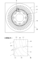
- FIG. 1 is a hypothetical diagram showing an example of separating a rotor core sheet and a stator core sheet from a silicon steel plate.
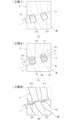
- FIG. 2 is a schematic diagram showing an example of a modification process applied to the silicon steel sheet.
- FIG. 13 is a schematic diagram showing another modified region (modified portion).
- FIG. 2 is a schematic diagram showing a modification process according to the embodiment.
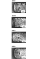
- 4 is a photograph showing the surface of a sample obtained in the modification process.
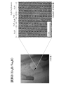
- 1 shows a TEM image and an XRD diffraction pattern of the B-based compound of sample 1.
- 1 shows a TEM image and an XRD diffraction pattern of the B-based compound of sample 2.
- 4 is a photograph showing the surface of a sample obtained in the modification process. 4 is a surface observation photograph of another sample obtained by the modification process. 1 is a photograph showing indentations formed in a modified region observed under a microscope.
- One or more components selected arbitrarily from the items described in this specification may be added to the configuration of the present invention described above.
- the components related to the method may also be components related to the object (electromagnetic steel sheet, core sheet, etc.). Which embodiment is best depends on the target, required performance, etc.
- the processing area may need to be expanded further to obtain a healthy modified area. This may result in restrictions on the shape of the modified area and removal area, or a decrease in the yield of the silicon steel sheet. Furthermore, the expansion of the modified area may increase the amount of heat input to the silicon steel sheet, which may lead to increased distortion of the electromagnetic steel sheet, and increased energy consumption and processing time.
- shrinkage cavities shrinkage holes, shrinkage tubes, external shrinkage, etc.
- solidification shrinkage liquid phase against the shrinkage (solidification shrinkage) when the liquid phase changes to a solid phase (especially in the final stage).
- High-temperature cracks are caused by insufficient supply of liquid phase, like shrinkage cavities, and grow due to tensile stress generated by solid-state shrinkage of the solidified solid phase.
- such a general theory does not simply apply to the case of the present invention, where the liquid phase (pocket) created by irradiation with a high-energy beam can be rapidly solidified immediately thereafter.
- the silicon steel plate and modifier When irradiated with a high-energy beam, the silicon steel plate and modifier instantly melt into a liquid phase (molten metal), and this liquid phase is rapidly cooled and solidified into a solid phase by the excessive heat of the surroundings. It is believed that a certain amount of B has a very large effect on this solidification process and, by extension, on the solidification structure. In other words, it is believed that B contributes greatly to improving the replenishment of the liquid phase (molten metal) to the solidification shrinkage area that occurs during the solidification process, and to the emergence of a high-strength metal structure that can withstand solidification shrinkage after solidification.
- the modified portion is made of a metal structure formed by melting and then solidifying.
- This metal structure includes an austenite phase and a compound phase.
- the austenite phase may be, for example, a primary crystal or may be part of a eutectic.
- the compound phase may be, for example, a part of a eutectic, or may not be.
- the type and amount of the compound phase that crystallizes or precipitates can vary depending on the iron alloy composition during melting and the modification process. From the perspective of preventing shrinkage cavities during melting and solidification, it is preferable for the density of the compound phase to be lower than that of the austenite phase. A low-density compound phase can compensate for the amount of solidification shrinkage that occurs when the austenite phase crystallizes, and can prevent the occurrence or coarsening of shrinkage cavities.
- B-based compounds are examples of such compound phases.
- B-based compounds include (Fe, Cr) 2 B, Fe 2 B, Cr 5 B 3 , Cr 2 B, and CrB. Incidentally, it is not easy to distinguish Fe from Cr in B-based compounds. There are cases where Fe-B compounds and Cr-B compounds are formed separately, and cases where Fe and Cr are mixed or combined to form a B compound ((Fe, Cr)-B compound). Furthermore, there are cases where other elements are incorporated.
- the compound phase may contain one or more of such B-based compounds.
- the densities (specific gravities) of the B-based compounds are, for example, Fe2B : 7.33 g/ cm3 , Cr5B3 : 6.46 g/ cm3 , Cr2B : 6.58 g/ cm3 , and CrB: 6.07 g/ cm3 .
- the density of the austenite phase varies depending on the component composition, but is about 7.8 to 7.9 g/ cm3 .
- the volume percentage of B-based compounds relative to the entire metal structure is, for example, 1-45% by volume (simply referred to as "%)", 2-40%, 6-30%, or 15-25%. If there are too few B-based compounds, shrinkage cavities are more likely to occur in the modified area. If there are too many B-based compounds, the modified area becomes brittle and hard, which can reduce the workability and lamination properties of the electromagnetic steel sheet.
- the volumetric percentage of B-based compounds can be found, for example, as follows.
- the volume and mass of a sample taken from the modified area are measured to determine its density ( ⁇ ).
- the ratio of the primary austenite phase and eutectic is measured based on the observed cross-sectional structure.
- the cross-sectional structure is observed using a metallurgical microscope or SEM.
- the area ratio of the austenite phase and multiple compound phases in the eutectic is measured from the results of observations using SEM, EDS, EPMA, TEM, STEM, etc. By converting the area ratio of each phase into a volume ratio, x and y can essentially be obtained.
- x and y can essentially be obtained.
- x and y can essentially be obtained.
- x and y can essentially be obtained.
- multiple compounds in the eutectic structure are identified using XRD, SAD analysis, STEM image analysis, etc., their densities can also be obtained from a known database. By determining the density in this way, it is also possible to avoid (substitute) measuring the area ratio of some compound phases.
- the B-based compound may be, for example, a complex compound in which at least two or more types of compounds are alternately formed.
- the compounds constituting the complex compound are, for example, two or more types such as Fe 2 B, Cr 2 B, FeCrB, Cr 5 B 3 , and CrB.
- the form of each compound that appears alternately may be granular or layered.
- the complex compound is layered.
- a specific example of such a complex compound is, for example, a complex compound in which Fe 2 B layers and Cr 2 B layers are alternately layered.
- the thickness of each layer observed from a microscopic photograph is, for example, 1 to 20 nm, 2 to 10 nm, or 3 to 5 nm.
- Silicon steel plate Silicon steel sheet is a (thin) plate material made of silicon steel. Silicon steel is an iron alloy containing 1-7%, 2-4%, or 2.5-3.5% Si based on the total content. Unless otherwise specified, the chemical composition in this specification is the mass percentage (mass%) based on the total content of the target, and is simply indicated by "%".
- Soft magnetic silicon steel is usually composed of Si with the remainder being Fe and (unavoidable) impurities, but may also contain alloying elements such as C, Mn, P, S, Ni, Al, Cr, Ca, and Mg. The total of these elements is, for example, 6% or less, or even 3% or less.
- iron alloys containing Si, regardless of whether or not C is present, are also referred to as "steel".
- the specific magnetic properties (magnetic permeability, saturation magnetization, etc.), structure, thickness, etc. of the silicon steel sheet can be selected as appropriate.
- a typical silicon steel sheet has, for example, a bcc crystal structure (ferrite phase) and its thickness is, for example, 0.1 to 1.0 mm or even 0.15 to 0.7 mm. If it is too thin, it may result in an increase in the number of layers (increased costs), a decrease in the strength of the modified area, and narrowing of the beam irradiation conditions. If it is too thick, it may result in increased iron loss and increased distortion due to the modification process.
- Silicon steel sheet may be non-oriented or oriented.
- non-oriented silicon steel sheet is used for electric motors (including generators/simply called “motors”); for example, oriented silicon steel sheet is used for transformers.
- At least one surface of the silicon steel sheet may be insulated. If an insulating coating (insulating film formation) is performed after the modification process, the insulating coating on the silicon steel sheet before the modification process may not be necessary.
- the modified portion is made of an iron alloy (referred to as a "modified alloy” as appropriate) with silicon steel as the base material (base material, raw material).
- the alloying elements include Si, B, Al, etc.
- an appropriate amount of alloying elements that stably generate the austenite phase, which is a non-magnetic phase, may be included.
- the composition of the alloying elements can be specified or adjusted, for example, based on the region that forms the austenite phase on the Schaeffler phase diagram (structural diagram).
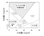
- the Schaeffler phase diagram shows the metal structures (F: ferrite phase, A: austenite phase, M: martensite) that appear in iron alloys, based on the Cr equivalent (horizontal axis) and Ni equivalent (vertical axis) shown below (see FIG. 5).
- an iron alloy having a composition within the region (hatched region in FIG. 5 ) that satisfies both of the following formulas (1) and (2) is mainly composed of an austenite phase and can exhibit non-magnetic (weak magnetic) properties. 0.78Creq+Nieq ⁇ 25.50 (1) 1.20Creq-Nieq ⁇ 8.43 (2)
- examples of alloying elements that contribute to the formation or stabilization of the austenite phase include Ni, Cr, Si, Mn, C, Mo, and Nb.
- the composition ranges of the representative elements Ni, Cr, Si, and Mn are shown as examples.
- the chemical composition of each element is the mass percentage of the entire modified alloy and is simply expressed as "%".
- Ni is contained, for example, at 10-30%, 13-27%, 15-25% or 17-23%.
- Cr is contained, for example, at 8-28%, 13-24%, 15-22% or 17-20%. If there is too little Ni or Cr, the austenite phase will decrease, and if there is too much, the raw material costs will increase.
- the silicon content is, for example, 1-5%, 1.3-4%, or 1.5-3%.
- silicon is a substitute for Cr. Excessive silicon hardens or embrittles the modified area.
- the lower limit of silicon depends on the chemical composition of the silicon steel plate, which is the base material.
- Mn is included, for example, at 20-60%, 26-54%, 30-50%, or 34-46%.
- Mn is a substitute for Ni. Mn can suppress cracking in the modified area, but if there is too little, the effect is small. Since Mn is easily evaporated in the liquid phase, excessive Mn can easily cause the composition of the modified area to fluctuate.
- B can prevent shrinkage cavities and high-temperature cracks from occurring in the modified region.
- B is contained in the entire modified alloy in an amount of, for example, 0.1-3%, 0.15-2.5%, 0.2-2%, 0.3-1.5%, 0.4-1.3%, or 0.5-1.1%. If there is too little B, the above-mentioned effects are poor, and if there is too much B, it can lead to embrittlement, hardening, and increased raw material costs. If there is too much B, cracks due to embrittlement are more likely to occur in the modified region when pressure is applied (for example, when stacking magnetic steel sheets) or when a high load is applied.
- the modified alloy may further contain an appropriate amount of Al. This can further prevent defects (particularly cracks) from occurring in the modified region.
- the amount of Al contained in the entire modified alloy is, for example, 0.5-5%, 1-4%, 1.5-3.5%, or 2-3%. If there is too little Al, the effect is poor, and if there is too much Al, it will harden the alloy and reduce its non-magnetic properties.
- the chemical components of the modified alloy are identified, for example, by analyzing a sample taken from approximately the center of the modified region (modified part) excluding the defective area.
- B is analyzed, for example, by an electron probe microanalyzer (EPMA).
- Other elements are analyzed, for example, by an energy dispersive spectroscopy (EDS).
- EDS energy dispersive spectroscopy
- the presence or absence or proportion of austenite phase contained in the modified part is analyzed by an X-ray diffraction device (XRD) or an electron backscatter diffraction device (EBSD).
- XRD X-ray diffraction device
- EBSD electron backscatter diffraction device
- the modification process is performed, for example, by irradiating a high-energy beam (also simply referred to as a "beam") onto a modifier disposed on a specific region of the silicon steel sheet.
- the modification process can form a modified portion including at least an austenite phase in a part of the silicon steel sheet.
- Modifier The modifier and the base material silicon steel plate are melted and mixed, then cooled and solidified to produce a modified alloy with the above-mentioned chemical composition.
- the modifier is supplied to a specific region of the silicon steel plate, for example, as a powder, ink (paste, slurry), sheet (film), etc.
- the powder is supplied onto a silicon steel plate, for example, by scraping.
- the powder is scraped off using a form placed on the silicon steel plate or a depression (recess) formed on the silicon steel plate.
- the ink (slurry) is applied onto the silicon steel plate, for example, by screen printing or inkjet printing.
- the sheet (film) is, for example, previously formed (punched, etc.) into the desired shape and then attached onto the silicon steel plate.
- a modifier consisting only of powder does not contain a solvent, a dispersion medium, a binder, etc., and the component composition of the modified alloy is easy to adjust.
- the modifier powder may be a single type or multiple types (mixed powder).
- the raw material powder constituting the modifier powder may be any of single element powders (Ni powder, Cr powder, B powder, Al powder, Mn powder, etc.), alloy powders (NiCr-based powder, FeB-based powder, FeAl-based powder, FeMn-based powder, etc.), powders of compounds (including intermetallic compounds) (Fe 2 B powder, FeAl 3 powder, etc.), etc.
- the component composition of the modifier and the amount of modifier supplied onto the silicon steel plate are adjusted taking into consideration the desired composition of the modifier alloy and the chemical composition and plate thickness of the silicon steel plate (base material).
- the thickness (height) should be, for example, about 0.1 to 1.4 mm, 0.2 to 1.0 mm, or 0.3 to 0.8 mm. If the thickness is too small or too large, the demagnetization of the modifier alloy may decrease.
- the plate thickness of silicon steel plate is usually about 0.15 to 0.7 mm.
- the high energy beam is, for example, a laser or an electron beam with a high energy density (fluence).
- the type (amplification medium, excitation source, optical resonator, etc.), output, energy density, irradiation area, overlap rate, etc. of the laser are appropriately selected and adjusted.
- the laser may be a continuous wave laser or a pulsed laser.
- One example of the laser is a fiber laser (a type of solid-state laser) that uses an optical fiber (for example, a double clad fiber with a rare earth element doped in the core) as the amplification medium.
- the fiber laser for example, has a semiconductor laser (LD) as an excitation source, and an optical reflection mirror on the input side and a low reflection mirror on the output side as an optical resonator.
- LD semiconductor laser
- the irradiation range and irradiation trajectory of the beam can be adjusted according to the desired shape of the modified portion. It is not necessary to melt the entire modifier placed on the silicon steel plate. The remaining modifier may be removed after the beam is irradiated.
- the end points (start point and end point) of the trajectory of the beam irradiation should be set (placed) in the removal area of the silicon steel plate. Near the end points, the molten mixture of the silicon steel plate and the modifier becomes unstable, and defects are likely to occur.
- a shaping process may be carried out to make the bead below the base surface (which may be flat or recessed).
- the shaping process may be carried out immediately after the modification process, or may be carried out together with the lamination process described below.
- the shaping process may also serve to remove thermal distortion of the silicon steel plate caused by beam irradiation.
- the area near the surface irradiated with the beam may be subjected to an insulating treatment.
- the insulating treatment may be, for example, the application of an insulating resin, a chemical treatment (e.g., phosphate treatment), etc.
- the insulating treatment process may be a processing process that forms an insulating space between opposing surfaces when stacked. The processing process may also serve as the shaping process described above.
- the order of the forming process for obtaining an electromagnetic steel sheet (sheet) of a desired shape from a silicon steel sheet does not matter. It is efficient to carry out the forming process after the reforming process.
- the forming process is, for example, a separation process (trimming) such as punching with a press or cutting (splitting, dividing, etc.) with a laser or the like.
- the order of the forming process and the above-mentioned shaping process and/or insulation process does not matter either. Finishing processes, etc. may be carried out after the forming process.
- the silicon steel sheets (electromagnetic steel sheets) having the modified portions and formed into the desired shape are stacked to form a laminate (stacking process). Multiple electromagnetic steel sheets are fixed together by crimping using a press process, welding, gluing, etc. The laminate may be subjected to additional finishing processes, etc., to ensure dimensional accuracy.
- An example of an application of an electromagnetic steel sheet is a core sheet.
- the core sheet is, for example, a rotor core sheet or a stator core sheet of an electric motor (including a generator).
- a laminate of rotor core sheets becomes a rotor core, and a laminate of stator core sheets becomes a stator core.
- Rotor core sheet 1 and stator core sheet 2 are punched out from a single silicon steel plate M.
- Rotor core sheet 1 and stator core sheet 2 are used to manufacture a rotor core (lamination/not shown) and a stator core (lamination/not shown) of an embedded magnet synchronous machine (called an "IPM motor").
- IPM motor embedded magnet synchronous machine
- the same reference numerals are used in each figure to indicate each part of silicon steel plate M before punching (imaginary parts shown by two-dot chain lines) and each part of silicon steel plate M after punching (actual parts shown by solid lines). Note that in the overall view of Figure 1A, even the imaginary parts are shown by solid lines for ease of display.
- the rotor core sheet 1 is for 8 magnetic poles. As shown in the enlarged view of part A, for each magnetic pole, approximately U-shaped slots 101, 102 for integrally molding the bonded magnet and bridges 111, 112 (connecting parts) are planned to be formed on the outer circumferential ends of the slots.
- the slots 101, 102 (slot areas) and the shaft hole 10 are areas that can be removed by punching (trimming) (areas to be removed), and the bridges 111, 112 (bridge areas) are areas that can remain after punching (trimming) (areas to be left).
- the modification process is performed on the area (modified area) including the bridge area before punching.
- the entire area or a part of each bridge (111, 112, etc.) created after punching is made into the modified area.
- the modified area created after punching is usually part of the modified area.
- the stator core sheet 2 is for 48 poles. For each pole, comb-tooth shaped teeth 211, 212 and slots 201, 202, 203 on either side of them are planned to be formed.
- the slots 201, 202, 203 (slot areas) before punching are the areas planned to be removed, while the teeth 211, 212 (teeth areas) and the yoke 21 are the areas planned to remain.
- only a portion selected as appropriate will be explained regarding each part of the rotor core sheet 1 and stator core sheet 2, and explanations of other parts that appear repeatedly in the circumferential direction will be omitted.
- modifiers 311, 312 are provided in and around the areas (Step I).
- the modifiers 311, 312 are, for example, powder layers formed by scraping off a mixture of CrNi alloy powder and FeB powder.
- the beam is irradiated from above the modifiers 311 and 312.
- the beam is irradiated by scanning the center of the beam along a trajectory t (specific trajectory) that passes through the areas that are to become the bridges 111 and 112, from a starting point p0 in the area that is to become the slots 101 and 102 on the rotor side to an end point p1 near the areas that are to become the slots 201, 202, and 203 on the stator side (Step II).
- a bead b (beam irradiation mark/modified area) is formed in the beam irradiation area, where the silicon steel plate M and the modifiers 311 and 312 are melted and mixed and cooled and solidified.
- the trajectory t of the beam irradiation is set so that at least one bead b is formed that penetrates the bridges 111, 112 in a substantially radial direction.
- the trajectory t is set so that the bead b formed on the bridges 111, 112 does not extend beyond the gap c created during punching to the stator core sheet 2 side.
- the beam irradiation may be performed from both sides (front and back sides) of the silicon steel plate M. However, even if the beam is only irradiated from one side of the silicon steel plate M, a bead (a bead that penetrates in the thickness direction) that reaches from one side of the silicon steel plate M to the other side can be formed.
- the silicon steel sheet M electromagnettic steel sheet
- the excess modifiers 311, 312 have been removed is punched using a die of a predetermined shape (step III).
- the rotor core sheet 1 having non-magnetic modified parts 121, 122 in parts of the bridges 111, 112 is obtained together with the stator core sheet 2.
- defects shrinkage cavities, cracks, unmelted parts, etc. formed near the start point p0 and end point p1 of the beam irradiation can be removed along with the formation of the slots 101, 102, etc.
- the more shrinkage cavities and cracks can be prevented and the smaller the defects can be made, the greater the degree of freedom in the shape of the modified part and the degree of freedom in setting the modified area can be expanded, and the yield of the silicon steel sheet can be improved, etc.
- Figure 1C shows an enlarged view of the case where the slot 101 of the rotor core sheet 1 is divided into two slots 1011 and 1012, one on the left and one on the right.
- non-magnetic modified parts 1211 and 1212 are formed in the bridges 1111 and 1112 in the outer peripheral end regions of the slots 1011 and 1012 by the modification process, as described above.
- modified part 1213 may also be formed in the bridge 1113 formed between the slots 1011 and 1012 (non-outer peripheral end region).
- the trajectory of the beam irradiation may be, for example, a straight path when viewed macroscopically, or a zigzag path when viewed microscopically.
- Base Material A silicon steel plate (Fe-3.1%Si-2.5%Ni/thickness: 0.5 mm/manufactured by Nippon Steel Corporation) was used as the base material.
- Modifier powder As raw material powders, Cr-50% Ni alloy powder (Well Powder manufactured by Nippon Welding Rod Co., Ltd.) and Fe-16% B powder (manufactured by Kojundo Chemical Laboratory Co., Ltd.) were prepared. These raw material powders were blended and mixed according to the desired composition of the modified region to produce a powder (referred to as "modifier powder") which was used as the modifier.
- a laser was irradiated onto the powder layer (modifier) excluding the frame plate, as shown in Fig. 2.
- a single-type fiber laser (laser generator: YLS-2000-SM manufactured by IPG Corporation, fiber core diameter: 24 ⁇ m, optical system: 3D galvanometer scanner manufactured by Yaskawa Electric Corporation, focusing diameter: 36 ⁇ m) was used.
- shrinkage cavity diameter The size of the shrinkage cavities that appeared in the modified area (simply referred to as "shrinkage cavity diameter") was measured using the circle measurement software of a one-shot 3D shape measuring instrument (VR-5000, manufactured by Keyence Corporation).
- the microstructures of Samples 1 and 2 observed under a metallurgical microscope confirmed the presence of a primary austenite phase and a eutectic.
- the primary austenite phase was dendritic, and the eutectic was composed of an austenite phase and a compound phase.
- the TEM image shown above shows the compound phase in the eutectic.
- Sample 3 also had a eutectic structure similar to that of Sample 1 and Sample 2.
- a part of the B-based compound phase in the eutectic of Sample 3 was further observed with a scanning transmission electron microscope (STEM/JEM-AEM200F manufactured by JEOL Ltd.) and a high angle annular dark field (HAADF) image obtained is shown in Figure 4C.
- STEM/JEM-AEM200F scanning transmission electron microscope
- HAADF high angle annular dark field
- the component analysis was performed as follows. B was analyzed using EPMA (EPMA-8050G, manufactured by Shimadzu Corporation). The other elements were analyzed using EDS (X-MAXN, manufactured by Oxford Instruments). The specific analysis conditions for each were as follows. An analysis sample ( ⁇ 25 mm) was prepared by cutting out an analysis portion (modified part) from a defect-free modified region, embedding it in resin, and polishing the cross section. Map analysis was performed on the central surface (100 ⁇ m x 100 ⁇ m) of the sample using EPMA for B. Map analysis was performed on the central surface (1000 ⁇ m x 300 ⁇ m) of the sample using EDS (voltage: 15 kV, current: 12 A) for the other components. The presence of austenite phase in the sample was confirmed by XRD.
- compositions of the austenite phase and the compound phase were identified by the above-mentioned component analysis. Based on this result, the density of the austenite phase ( ⁇ a) and the density of the compound phase ( ⁇ b, ⁇ c) were determined by quoting from an existing crystal structure database. In addition, the density ( ⁇ ) of the sample (modified part) taken from the modified region was previously obtained by the Archimedes method. From these, the content (volume %) of the compound phase was calculated. The type (composition) and the content of the compound phase are also shown in Table 1. Note that the entire sample 4 was an austenite phase, and no compound phase (eutectic) was observed.
- the identification (presence or absence) of the configuration according to the present invention can be determined by analyzing and analyzing the modified portion in a microscopic region (region defined in ⁇ m units), which is the general subject of analysis. Observation and analysis of the modified portion in an ultra-small region (region defined in nm units, e.g., 10 nm x 10 nm or 5 nm x 5 nm) can be performed appropriately and to the extent necessary.
- the base material was the above-mentioned silicon steel plate (Fe-3.1%Si-2.5%Ni/thickness: 0.5 mm).
- FIG. 6A and FIG. 6B Observation Photographs of the surface observation of the modified regions of each sample are shown in FIG. 6A and FIG. 6B (collectively referred to as "FIG. 6").
- the component analysis was performed as follows. B was analyzed using EPMA (EPMA-8050G, manufactured by Shimadzu Corporation). The other elements were analyzed using EDS (X-MAXN, manufactured by Oxford Instruments). The specific analysis conditions for each were as follows. A sample ( ⁇ 25 mm) for analysis was prepared by cutting out an analysis portion (modified part) from a defect-free modified region, embedding it in resin, and polishing the cross section. Map analysis was performed on the central surface (100 ⁇ m x 100 ⁇ m) of the sample using EPMA for B. Map analysis was performed on the central surface (1000 ⁇ m x 300 ⁇ m) of the sample using EDS (voltage: 15 kV, current: 12 A) for the other components. The presence of austenite phase in the sample was confirmed by XRD.
- Indentation test The brittleness of the modified region of each sample was evaluated by an indentation test.
- the indentation test was performed by pressing a diamond pyramid (indenter) against the modified region, with reference to the Vickers hardness test (JIS Z2244).
- the test load was 100 gf.
- Figure 7 shows an example of an optical microscope photograph of the indentations made in the modified regions of some of the samples.
- the cracks started at the corners of the indentations and extended in a short, approximately straight line.
- the crack lengths (the total length if there were multiple cracks) were measured at three different locations in the modified regions of each sample using a linear approximation.
- the crack lengths for each sample thus determined are also shown in Table 2.
Landscapes
- Chemical & Material Sciences (AREA)
- Engineering & Computer Science (AREA)
- Materials Engineering (AREA)
- Power Engineering (AREA)
- Physics & Mathematics (AREA)
- Organic Chemistry (AREA)
- Metallurgy (AREA)
- Mechanical Engineering (AREA)
- Electromagnetism (AREA)
- Crystallography & Structural Chemistry (AREA)
- Thermal Sciences (AREA)
- Dispersion Chemistry (AREA)
- Immunology (AREA)
- Pathology (AREA)
- General Physics & Mathematics (AREA)
- General Health & Medical Sciences (AREA)
- Biochemistry (AREA)
- Analytical Chemistry (AREA)
- Life Sciences & Earth Sciences (AREA)
- Health & Medical Sciences (AREA)
- Manufacturing & Machinery (AREA)
- Soft Magnetic Materials (AREA)
Abstract
ケイ素鋼板の一部に改質部を有する電磁鋼板を提供する。本発明は、溶融凝固してできた改質部を一部に有するケイ素鋼板である。この改質部は、オーステナイト相と化合物相を含む金属組織を有する。その化合物相は、オーステナイト相よりも低密度なB系化合物を含むとよい。また本発明は、ケイ素鋼板の特定領域上に配置した改質材へ高エネルギービームを照射して、少なくともオーステナイト相を含む改質部をケイ素鋼板の一部に形成する改質工程を備える電磁鋼板の製造方法である。その改質部にはBが、例えば、0.15~3質量%さらには0.3~1.5質量%含まれるとよい。
Description
本発明は、改質部を有する電磁鋼板等に関する。
交番磁界中で使用される磁性部材の多くは、磁気回路の形成、渦電流損失(鉄損)の抑制、強度の確保等のため、所定形状に成形された電磁鋼板の積層体からなる。磁性部材のさらなる高性能化や低損失化(効率化)等を図るため、積層体の一部が非磁性(弱磁性、低磁性を含む。)にされることも多い。
例えば、電動機(モータ、ジェネレータ)のロータやステータは、通常、所望形状に成形(打ち抜き、溶断等のトリミング)されたケイ素鋼板からなるコアシートを積層してなる。起磁源である永久磁石を収容するスロットの外周側にできる狭幅なブリッジ(連結部)は、改質により非磁性化されて、回転トルクに寄与しない無効な磁束の低減が図られる。
このような改質は、積層前または積層後のケイ素鋼板の金属組織(フェライト相)をオーステナイト相を含む金属組織へ変態させてなされ得る。これに関連する記載が、例えば、下記の特許文献にある。
特許文献1は、磁気検出に用いるステンレス鋼製リング上に、合金粉末をレーザ光照射により溶融凝固させた肉盛層を形成して、領域毎に磁気特性を変化(改質)させている。改質に際して、3相(フェライト相、オーステナイト相、マルテンサイト相)の存在域を、Ni当量とCr当量を軸とする座標上に示したシェフラー状態図が参考にされている。
特許文献2は、ステンレス鋼からなる電磁アクチュエータ(燃料噴射弁)用固定鉄心にレーザ照射をして、フェライト相や加工誘起マルテンサイト相を非磁性なオーステナイト相へ変態させることを提案している。特許文献1や特許文献2には、ケイ素鋼板の改質に関する記載は一切ない。
特許文献3は、Mn―Ni―B合金粉末とメチルセルロース水溶液を混合したペーストを所定域に塗布したケイ素鋼板を加熱炉で加熱(1120℃×20分間)し、ケイ素鋼板の所定域を非磁性化している(特許文献3の実施例4)。緩慢な加熱により合金粉末をケイ素鋼板へ溶け込ませてできる金属組織は、合金粉末とケイ素鋼板を共に溶融させた後に凝固させてできる金属組織とは大きく異なる。
特許文献4は、Ni―Cr粉末をテトラデカンに分散させたインクを電磁鋼板に印刷した後、乾燥後のインクへ電子ビーム照射する局所加熱(1520℃×1秒間)により、溶融合金化された非磁性領域を電磁鋼板上に形成している。特許文献4には、レーザ照射による局所加熱や、B添加による溶融合金化温度の低減に関する言及もあるが、それらに関する具体的な記載(例えばB量)は一切ない。
特許文献5は、Fe―Cr―C系合金板(強磁性素材)から切り出して形成されたロータコアシートを外周側から高周波加熱して、外周側にある狭幅な連結部(ブリッジ)だけを非溶融のままオーステナイト主体の金属組織(弱磁性部)へ変態させることを提案している。特許文献5にも、ケイ素鋼板の改質に関する記載は一切ない。
特許文献6は、磁性体を非磁性体へ改質する加熱条件(入熱量)に関する提案をしている。特許文献6にも、ケイ素鋼板の改質に関する具体的な記載は一切ない。
特許文献7、8には、ロータコアのブリッジに改質部を設ける旨の記載がある。特許文献7は、レーザ照射(加熱)により電磁鋼板の透磁率を部分的に低下させているに過ぎない。特許文献8は、ケイ素鋼板(母材)と改質材(ニッケル、クロム等)とをレーザ溶融して、オーステナイト相からなる改質部を形成している。しかし、その改質部の組織構造や成分組成等に関する具体的な記載は特許文献8にない。
本発明はこのような事情に鑑みて為されたものであり、ケイ素鋼板の一部に改質部を設けた新たな電磁鋼板またはその製造方法等を提供することを目的とする。
本発明者は鋭意研究した結果、ケイ素鋼板の一部に設けた改質部が、特定の成分組成(B量)や金属組織を有するとき、歩留まりよく所望特性の電磁鋼板が得られた。この成果を発展させることにより、以降に述べる本発明を完成するに至った。
《電磁鋼板》
本発明は、少なくともオーステナイト相を含む改質部を、一部に有するケイ素鋼板からなり、該改質部全体に対してBが0.15~3質量%含まれる電磁鋼板である。
本発明は、少なくともオーステナイト相を含む改質部を、一部に有するケイ素鋼板からなり、該改質部全体に対してBが0.15~3質量%含まれる電磁鋼板である。
このような改質部は、例えば、オーステナイト相と化合物相を含む金属組織を有し、該化合物相は、Bを含むB系化合物を含み、該B系化合物は、該オーステナイト相よりも低密度となる。
ケイ素鋼板の一部を溶融凝固させて改質する場合なら、上述した改質部の形成領域(改質域)における割れまたは引け巣等の発生が抑止される。これにより、改質部の形態自由度の拡大、改質域の設定自由度の拡大またはケイ素鋼板の歩留まり向上等が図られ得る。オーステナイト相に加えて、化合物相も非磁性であるとよい。
特に断らない限り、本明細書でいう「ケイ素鋼板」は、素材、基材または母材を意味し、その形態や、処理または加工の有無等を問わない。また「電磁鋼板」は、少なくとも一部が改質(処理)されたケイ素鋼板、または少なくとも一部に改質部を有するケイ素鋼板を意味する。このような電磁鋼板は、成形等の加工前の状態でも、その加工後の状態でもよい。改質と加工の先後は問わない。
《電磁鋼板の製造方法》
本発明は、電磁鋼板の製造方法としても把握でき、ケイ素鋼板の特定領域上に配置した改質材へ高エネルギービームを照射して、該ケイ素鋼板の一部に改質部を形成する改質工程を備え、所望の電磁鋼板を得る製造方法でもよい。
本発明は、電磁鋼板の製造方法としても把握でき、ケイ素鋼板の特定領域上に配置した改質材へ高エネルギービームを照射して、該ケイ素鋼板の一部に改質部を形成する改質工程を備え、所望の電磁鋼板を得る製造方法でもよい。
この改質工程により、例えば、少なくともオーステナイト相を含む改質部が該ケイ素鋼板の一部に形成される。改質部の全体に対してBが0.15~3質量%含まれる場合、例えば、改質処理する領域(改質域)の縮小化、ケイ素鋼板の歩留まり向上(除去加工域の自由度拡大)、改質部の形態自由度の拡大または電磁鋼板に生じる歪みや凹凸の抑制等を図ることもできる。
《磁性部材と電磁機器》
(1)本発明は、電磁鋼板を用いた磁性部材や電磁機器としても把握される。例えば、本発明は、上述した改質部を一部に有するケイ素鋼板からなるコアシートでもよい。コアシートは、その形態を問わず、改質部が形成されたケイ素鋼板であれば、トリミング(例えば打抜き)等の加工前でも、その加工後(積層可能な形態)でもよい。
(1)本発明は、電磁鋼板を用いた磁性部材や電磁機器としても把握される。例えば、本発明は、上述した改質部を一部に有するケイ素鋼板からなるコアシートでもよい。コアシートは、その形態を問わず、改質部が形成されたケイ素鋼板であれば、トリミング(例えば打抜き)等の加工前でも、その加工後(積層可能な形態)でもよい。
(2)本発明は、電磁鋼板(コアシート等)を積層した部材や、それを用いた装置としても把握される。例えば、本発明は、複数の電磁鋼板を積層したコア(磁心)でもよい。コアは、例えば、電動機を構成するロータコアおよび/またはステータコアである。また本発明は、そのようなロータコアやステータコアと、永久磁石や電磁コイル(アーマチャ)とを組み合わせたロータやステータでもよい。このような一例として、ロータコアの磁石孔に永久磁石が埋め込まれた磁石内包型ロータ(例えばIPM用ロータ)がある。
さらに本発明は、上述した電磁鋼板(コアシート)からなるロータおよび/またはステータを備えた電動機(発電機を含む)でもよい。
《その他》
(1)本明細書でいう「非磁性」は、母材であるケイ素鋼板よりも磁化され難いこと(磁束を通し難いこと)を意味する。その具体的な程度は問わず、「弱磁性」または「低磁性」も含めて「非磁性」という。このような非磁性な領域(非磁性域)をケイ素鋼板の一部に形成することを、本明細書では「改質」または「非磁性化」という。
(1)本明細書でいう「非磁性」は、母材であるケイ素鋼板よりも磁化され難いこと(磁束を通し難いこと)を意味する。その具体的な程度は問わず、「弱磁性」または「低磁性」も含めて「非磁性」という。このような非磁性な領域(非磁性域)をケイ素鋼板の一部に形成することを、本明細書では「改質」または「非磁性化」という。
非磁性に改質された領域(改質域)は、母材であるケイ素鋼板に対して、(初)透磁率の低下、飽和磁束密度の低下、磁気抵抗の増大等により判断される。改質域の一部または全部である改質部には、通常、ケイ素鋼板のフェライト相が変態してできたオーステナイト相が含まれる。改質部の全体がオーステナイト相でもよいし、改質部の一部にそれ以外の他相(フェライト相、マルテンサイト相、化合物相等)が含まれてもよい。
(2)特に断らない限り本明細書でいう「x~y」は下限値xおよび上限値yを含む。本明細書に記載した種々の数値または数値範囲に含まれる任意の数値を新たな下限値または上限値として「a~b」のような範囲を新設し得る。また、特に断らない限り、本明細書でいう「x~yμm」はxμm~yμmを意味する。他の単位系(mm等)についても同様である。
本明細書中に記載した事項から任意に選択した一つまたは二つ以上の構成要素を上述した本発明の構成に付加し得る。方法に関する構成要素も物(電磁鋼板、コアシート等)に関する構成要素となり得る。いずれの実施形態が最良であるか否かは、対象、要求性能等によって異なる。
《本発明の経緯と機序》
本発明の完成に至った経緯と、特定の成分組成(B量)や金属組織を有する電磁鋼板が優れた効果を発現する機序は次のように考えられる。
本発明の完成に至った経緯と、特定の成分組成(B量)や金属組織を有する電磁鋼板が優れた効果を発現する機序は次のように考えられる。
(1)経緯
ケイ素鋼板は、通常、所望形状に成形(打ち抜き等のトリミング)されるため、多かれ少なかれ除去される部分(除去域)が生じる。改質により欠陥(引け巣、割れ等)が生じても、その欠陥を包括する領域(欠陥域)が除去域内にある限り、基本的に電磁鋼板自体の不良とはならず、その品質は確保され得る。
ケイ素鋼板は、通常、所望形状に成形(打ち抜き等のトリミング)されるため、多かれ少なかれ除去される部分(除去域)が生じる。改質により欠陥(引け巣、割れ等)が生じても、その欠陥を包括する領域(欠陥域)が除去域内にある限り、基本的に電磁鋼板自体の不良とはならず、その品質は確保され得る。
もっとも、欠陥域が拡大すると、所望の改質部の確保が困難になったり、健全な改質部を確保するために処理域(改質域)の余計な拡張が必要になる。その結果、改質部や除去域の形状制限やケイ素鋼板の歩留まり悪化等が生じ得る。また、改質域の拡張は、ケイ素鋼板への入熱量の増加となり、電磁鋼板の歪み等の拡大、エネルギー消費量や加工時間の増加等が生じ得る。
(2)機序
改質域に所定量のBが含まれるとき、改質に伴い生じ得る引け巣や割れ等の欠陥域が大幅に縮小されるが、現状、その理由は定かではない。一般的な鋳物に関していえば、引け巣(収縮空孔、収縮管、外ひけ等)は、液相が固相へ変化するとき(特に最終段階)の収縮(凝固収縮)に対する液相の補給不足に起因して生じる。(高温)割れは、引け巣と同様に液相の補給不足に起因して生じ、凝固した固相の固体収縮により発生する引張応力により成長する。しかし、このような一般論が、高エネルギービームの照射によりできた液相(湯溜り)が、その直後に急速凝固し得る本発明のような場合にまで、単純に当てはまる訳ではない。
改質域に所定量のBが含まれるとき、改質に伴い生じ得る引け巣や割れ等の欠陥域が大幅に縮小されるが、現状、その理由は定かではない。一般的な鋳物に関していえば、引け巣(収縮空孔、収縮管、外ひけ等)は、液相が固相へ変化するとき(特に最終段階)の収縮(凝固収縮)に対する液相の補給不足に起因して生じる。(高温)割れは、引け巣と同様に液相の補給不足に起因して生じ、凝固した固相の固体収縮により発生する引張応力により成長する。しかし、このような一般論が、高エネルギービームの照射によりできた液相(湯溜り)が、その直後に急速凝固し得る本発明のような場合にまで、単純に当てはまる訳ではない。
ケイ素鋼板と改質材は、高エネルギービームの照射により瞬時に溶融して液相(溶湯)となり、その液相は周囲への拔熱により急冷凝固した固相となる。所定量のBが、そのような凝固過程、ひいては凝固組織に及ぼす影響が非常に大きいと考えられる。つまりBは、凝固過程で生じる凝固収縮域への液相(溶湯)の補充性の改善、凝固後の固体収縮に耐え得る高強度な金属組織の出現等に、大きく寄与していると考えられる。
《金属組織》
(1)改質部は、溶融後に凝固してできた金属組織からなる。この金属組織は、オーステナイト相と化合物相を含む。オーステナイト相は、例えば、初晶でもよいし、共晶の一部でもよい。化合物相は、例えば、共晶の一部でもよいし、そうでなくてもよい。
(1)改質部は、溶融後に凝固してできた金属組織からなる。この金属組織は、オーステナイト相と化合物相を含む。オーステナイト相は、例えば、初晶でもよいし、共晶の一部でもよい。化合物相は、例えば、共晶の一部でもよいし、そうでなくてもよい。
晶出または析出する化合物相は、溶融時の鉄合金組成や改質工程等に応じて、種類や量が変化し得る。溶融凝固時の引け巣を抑止する観点からいうなら、オーステナイト相よりも低密度であるとよい。低密度な化合物相は、オーステナイト相が晶出するときに生じる凝固収縮量を補って、引け巣の発生またはその粗大化を抑止し得る。
(2)このような化合物相として、例えば、B系化合物がある。B系化合物には、(Fe、Cr)2B、Fe2B、Cr5B3 、Cr2B、CrB等がある。ちなみに、B系化合物中におけるFeとCrの峻別は容易ではない。Fe-B化合物とCr-B系化合物が個別に形成されている場合もあれば、FeとCrが混在または複合化してB化合物((Fe、Cr)-B化合物)を形成している場合もあり得る。さらには、別な元素が取り込まれている場合もあり得る。
化合物相は、そのようなB系化合物の一種以上を含めばよい。B系化合物の密度(比重)は、例えば、Fe2B:7.33g/cm3、Cr5B3:6.46g/cm3、Cr2B:6.58g/cm3、CrB:6.07g/cm3 である。なお、オーステナイト相の密度は、その成分組成により異なるが、7.8~7.9g/cm3程度である。
B系化合物は、金属組織全体に対する体積割合で、例えば、1~45体積%(単に「%」という。)、2~40%、6~30%または15~25%含まれる。B系化合物が過少では、改質域に引け巣が生じ易くなる。B系化合物が過多になると、改質部の脆化や硬質化により、電磁鋼板の加工性や積層性等が低下し得る。
B系化合物の体積割合は、例えば、次のようにして求められる。改質部から採取した試料の体積と質量を測定し、その密度(ρ)を求める。X線回折分析(XRD)、電子プローブマイクロアナライザー(EPMA)、エネルギー分散型線分光分析(EDS、EDX)等により、試料に含まれるB系化合物の種類やオーステナイト相(母相)の種類を特定する。これにより、オーステナイト相の密度(ρa)とB系化合物の密度(ρb)が、既知のデータベースから求まる。あるB系化合物の体積割合をx(0<x<1)とすると、ρ=(1-x)ρa+xρbを解いて、そのB系化合物の体積割合(100x(%))が求まる。
金属組織中に複数種の化合物が含まれる場合は次のように考えるとよい。例えば、上記のB系化合物に加えて2種目の化合物(別なB系化合物等)が含まれるときなら、その密度:ρc、その体積割合:y(0<y<1)として、ρ=(1-x-y)ρa+xρb+yρcと表現される。但し、変数の増加に伴い、別な測定が必要になる。
例えば、観察した断面組織に基づいて、初晶となるオーステナイト相と共晶の割合を測定する。断面組織は、金属顕微鏡やSEMにより観察される。さらに、SEM、EDS、EPMA、TEM、STEMなどの観察結果から、共晶中におけるオーステナイト相と複数種の化合物相との面積割合を測定する。各相の面積割合を体積割合へ換算すれば、実質的にx、yを求めることができる。その他、共晶組織にある複数種の化合物は、XRD、SAD分析、STEM像解析などで同定すれば、それらの密度も既知のデータベースから求まる。このような密度の特定により、一部の化合物相の面積割合の測定を回避(代替)することもできる。
(3)改質部に含まれるB系化合物の具体的な態様(種類数、成分組成、形状等)は問わない。一例として、B系化合物は、例えば、少なくとも二種以上の化合物が交互に形成された複化合物でもよい。複化合物を構成する化合物(「構成化合物」という。)は、例えば、Fe2B、Cr2B、FeCrB、Cr5B3 、CrB等の二種以上である。交互に現れる各化合物の形態は粒状でも層状でもよい。層状な構成化合物が交互に出現する場合、複化合物は積層状となる。その具体例として、例えば、Fe2B層とCr2B層が交互に積層された複化合物がある。顕微鏡写真から観察される各層の厚さは、例えば、1~20nm、2~10nmまたは3~5nmである。
《ケイ素鋼板》
ケイ素鋼板は、ケイ素鋼からなる(薄)板材である。ケイ素鋼は、その全体に対してSiを1~7%、2~4%または2.5~3.5%を含む鉄合金である。本明細書でいう化学成分は、特に断らない限り、その対象全体に対する質量割合(質量%)であり、単に「%」で示す。
ケイ素鋼板は、ケイ素鋼からなる(薄)板材である。ケイ素鋼は、その全体に対してSiを1~7%、2~4%または2.5~3.5%を含む鉄合金である。本明細書でいう化学成分は、特に断らない限り、その対象全体に対する質量割合(質量%)であり、単に「%」で示す。
軟磁性であるケイ素鋼は、通常、Siと残部であるFeおよび(不可避)不純物とからなるが、C、Mn、P、S、Ni、Al、Cr、Ca、Mg等の合金元素が含まれてもよい。それらの合計は、例えば、6%以下さらには3%以下である。なお、本明細書では、Cの有無を問わず、Siを含む鉄合金も「鋼」という。
ケイ素鋼板の具体的な磁気特性(透磁率、飽和磁化等)、組織、厚さ等は、適宜選択され得る。代表的なケイ素鋼板は、例えば、bcc結晶構造(フェライト相)からなり、その厚さは、例えば、0.1~1.0mmさらには0.15~0.7mmである。薄過ぎると、積層数の増加(コスト増加)、改質部の強度低下、ビームの照射条件の狭小化等が生じ得る。厚過ぎると、鉄損の増加、改質工程による歪みの増加等が生じ得る。
ケイ素鋼板は、無方向性でも方向性でもよい。電動機(発電機を含む/単に「モータ」という。)には、例えば、無方向性ケイ素鋼板が用いられる。変圧器(トランス)等には、例えば、方向性ケイ素鋼板が用いられる。ケイ素鋼板は、少なくとも一方の表面が絶縁被覆されていてもよい。改質工程後に絶縁被覆(絶縁膜形成)を行なうなら、改質工程前のケイ素鋼板における絶縁被覆は無くてもよい。
《改質部》
(1)改質部は、ケイ素鋼を基材(母材、原料)とする鉄合金(適宜「改質合金」という。)からなる。その合金元素として、Siの他、B、Al等がある。その他、非磁性相となるオーステナイト相を安定的に生成させる合金元素が適量含まれてもよい。
(1)改質部は、ケイ素鋼を基材(母材、原料)とする鉄合金(適宜「改質合金」という。)からなる。その合金元素として、Siの他、B、Al等がある。その他、非磁性相となるオーステナイト相を安定的に生成させる合金元素が適量含まれてもよい。
(2)合金元素の成分組成は、例えば、シェフラーの状態図(組織図)上でオーステナイト相を形成する領域に基づいて特定または調整され得る。シェフラーの状態図は、下記に示すCr当量(横軸)とNi当量(縦軸)を基軸として、鉄合金に現れる金属組織(F:フェライト相、A:オーステナイト相、M:マルテンサイト)を示している(図5参照)。
Ni当量(Nieq)=[Ni]+30[C]+0.5[Mn]
Cr当量(Creq)=[Cr]+[Mo]+1.5[Si]+0.5[Nb]
([X]は、鉄合金中に含まれる合金元素Xの含有量(質量%)を示す。)
Ni当量(Nieq)=[Ni]+30[C]+0.5[Mn]
Cr当量(Creq)=[Cr]+[Mo]+1.5[Si]+0.5[Nb]
([X]は、鉄合金中に含まれる合金元素Xの含有量(質量%)を示す。)
シェフラーの状態図に基づけば、下式(1)、(2)を共に満たす領域内(図5のハッチング域)にある成分組成の鉄合金は、主にオーステナイト相からなり、非磁性(弱磁性)を発現し得る。
0.78Creq+Nieq≧25.50 (1)
1.20Creq-Nieq≦8.43 (2)
0.78Creq+Nieq≧25.50 (1)
1.20Creq-Nieq≦8.43 (2)
シェフラーの状態図からもわかるように、オーステナイト相の形成または安定化に寄与する合金元素として、例えば、Ni、Cr、Si、Mn、C、Mo、Nb等がある。ここでは、代表的なNi、Cr、Si、Mnについて、それらの組成範囲を例示する。各元素の化学成分は、改質合金全体に対する質量割合であり単に「%」で表記する。
Niは、例えば、10~30%、13~27%、15~25%または17~23%含まれる。Crは、例えば、8~28%、13~24%、15~22%または17~20%含まれる。NiやCrが過少ではオーステナイト相が減少し、それらが過多では原料コストが増加する。
Siは、例えば、1~5%、1.3~4%または1.5~3%含まれる。Siは、Cr当量式からわかるように、Crの代替となる。過多なSiは改質部を硬質化または脆化させる。Siの下限値は母材であるケイ素鋼板の化学組成に依存する。
Mnは、例えば、20~60%、26~54%、30~50%または34~46%含まれる。Mnは、Ni当量式からわかるように、Niの代替となる。Mnは改質域の割れを抑制し得るが、過少ではその効果が乏しい。Mnは液相で蒸発しやすいため、過多なMnは改質部の成分が変動し易くなる。
(3)Bは、引け巣や高温割れ(クラック)等が改質域で発生することを抑止し得る。Bは、改質合金全体に対して、例えば、0.1~3%、0.15~2.5%、0.2~2%、0.3~1.5%、0.4~1.3%または0.5~1.1%含まれる。Bが過少では上述した効果が乏しく、Bが過多では脆化、硬質化、原料コスト増加等を招く。Bが過多になると、加圧時(例えば電磁鋼板の積層時)や高荷重作用時などに、脆化に依るクラックが改質部に生じ易くなる。
改質合金は、さらにAlを適量含んでもよい。これにより改質域における欠陥(特に割れ)の発生をさらに抑止し得る。Alは、改質合金全体に対して、例えば、0.5~5%、1~4%、1.5~3.5%または2~3%含まれる。Alは過少では、その効果が乏しく、Alが過多では硬質化や非磁性の低下を招く。
(4)改質合金の化学成分は、例えば、欠陥域を除いた改質域(改質部)の略中央付近から採取したサンプルを分析して特定される。Bは、例えば、電子プローブマイクロアナライザー(EPMA)により分析される。その他の元素は、例えば、エネルギー分散型分光装置(EDS)により分析される。改質部に含まれるオーステナイト相の有無または割合は、X線回折装置(XRD)または電子後方散乱回折装置(EBSD)により分析される。
《改質工程》
改質工程は、例えば、ケイ素鋼板の特定領域上に配置した改質材へ高エネルギービーム(単に「ビーム」ともいう。)を照射してなされる。改質工程により、ケイ素鋼板の一部に、少なくともオーステナイト相を含む改質部が形成され得る。
改質工程は、例えば、ケイ素鋼板の特定領域上に配置した改質材へ高エネルギービーム(単に「ビーム」ともいう。)を照射してなされる。改質工程により、ケイ素鋼板の一部に、少なくともオーステナイト相を含む改質部が形成され得る。
(1)改質材
改質材と母材であるケイ素鋼板とが溶融混合後に冷却凝固されて、上述した化学成分の改質合金ができる。改質材は、例えば、粉末、インク(ペースト、スラリー)、シート(フィルム)等として、ケイ素鋼板の特定領域に供給される。
改質材と母材であるケイ素鋼板とが溶融混合後に冷却凝固されて、上述した化学成分の改質合金ができる。改質材は、例えば、粉末、インク(ペースト、スラリー)、シート(フィルム)等として、ケイ素鋼板の特定領域に供給される。
粉末は、例えば、擦切り等によりケイ素鋼板上に供給される。粉末の擦切りは、ケイ素鋼板上に載置した型枠やケイ素鋼板上に形成した窪み(凹部)等を利用してなされる。インク(スラリー)は、例えば、スクリーン印刷、インクジェット印刷等によりケイ素鋼板上に塗布される。シート(フィルム)は、例えば、予め所望形状に成形(型抜き等)された状態でケイ素鋼板上に貼着される。
粉末のみからなる改質材(「改質粉末」という。)は、溶媒、分散媒、結合剤等を含まず、改質合金の成分組成を調整し易い。改質粉末は、単種でも複数種(混合粉末)でもよい。改質粉末を構成する原料粉末は、単元素粉末(Ni粉末、Cr粉末、B粉末、Al粉末、Mn粉末等)、合金粉末(NiCr系粉末、FeB系粉末、FeAl系粉末、FeMn系粉末等)、化合物(金属間化合物を含む)の粉末(Fe2B粉末、FeAl3粉末等)等のいずれでもよい。
改質材の成分組成や改質材のケイ素鋼板上への供給量は、改質合金の所望組成およびケイ素鋼板(母材)の化学組成と板厚を考慮して調整される。なお、ケイ素鋼板上に改質粉末を層状に形成する場合、その厚さ(高さ)は、例えば、0.1~1.4mm、0.2~1.0mmまたは0.3~0.8mm程度とするとよい。その厚さが過小でも過大でも、改質合金の非磁性化が低下し得る。ちなみに、ケイ素鋼板の板厚は、通常、0.15~0.7mm程度である。
(2)高エネルギービーム
高エネルギービームは、例えば、エネルギー密度(フルエンス)が大きいレーザや電子ビームである。レーザは、種類(増幅媒質、励起源、光共振器等)、出力、エネルギー密度、照射エリア、オーバーラップ率等が適宜、選択・調整される。レーザは、連続波レーザでもパルスレーザでもよい。レーザの一例として、増幅媒質に光ファイバー(例えば、コアに希土類元素をドープしたダブルクラッドファイバー)を用いたファイバーレーザ(固体レーザの一種)がある。ファイバーレーザは、例えば、半導体レーザ(LD)を励起源として、入射側の光反射ミラーと出力側の低反射ミラーとを光共振器として備える。
高エネルギービームは、例えば、エネルギー密度(フルエンス)が大きいレーザや電子ビームである。レーザは、種類(増幅媒質、励起源、光共振器等)、出力、エネルギー密度、照射エリア、オーバーラップ率等が適宜、選択・調整される。レーザは、連続波レーザでもパルスレーザでもよい。レーザの一例として、増幅媒質に光ファイバー(例えば、コアに希土類元素をドープしたダブルクラッドファイバー)を用いたファイバーレーザ(固体レーザの一種)がある。ファイバーレーザは、例えば、半導体レーザ(LD)を励起源として、入射側の光反射ミラーと出力側の低反射ミラーとを光共振器として備える。
ビームの照射範囲や照射軌跡は、所望する改質部の形態に応じて調整され得る。必ずしも、ケイ素鋼板上に配置した改質材全体を溶融させなくてもよい。残存した改質材は、ビーム照射後に除去されてもよい。ビームを照射する軌跡の端点(始点や終点)は、ケイ素鋼板の除去域に設定(配置)されるとよい。その端点付近では、ケイ素鋼板と改質材の溶融混合が不安定となり、欠陥ができ易い。
《他工程》
(1)ビームの照射痕(適宜「ビード」という。)が、ケイ素鋼板の基面(非改質表面)から盛り上がっているとき、それを基面以下(平坦状態でも、さらに窪んだ状態でもよい。)にする整形工程を行なってもよい。整形工程は、改質工程の直後になされてもよいし、後述する積層工程の際に併せてなされてもよい。整形工程は、ビーム照射により生じたケイ素鋼板の熱歪み等の除去を兼ねてもよい。
(1)ビームの照射痕(適宜「ビード」という。)が、ケイ素鋼板の基面(非改質表面)から盛り上がっているとき、それを基面以下(平坦状態でも、さらに窪んだ状態でもよい。)にする整形工程を行なってもよい。整形工程は、改質工程の直後になされてもよいし、後述する積層工程の際に併せてなされてもよい。整形工程は、ビーム照射により生じたケイ素鋼板の熱歪み等の除去を兼ねてもよい。
(2)ビーム照射された表面付近は絶縁処理がなされてもよい。絶縁処理は、例えば、絶縁樹脂塗布、化成処理(例えばリン酸塩処理)等である。絶縁処理工程は、積層時の対面間に絶縁空間を形成する加工工程でもよい。加工工程は、上述した整形工程を兼ねてもよい。
(3)ケイ素鋼板から所望形状の電磁鋼板(シート)を得る成形工程と改質工程の前後関係は問わない。改質工程後に、成形工程がなされると効率的である。成形工程は、例えば、プレスによる打抜き加工、レーザ等による切断(分割、分断等)加工などの分離工程(トリミング)である。成形工程と上述した整形工程および/または絶縁処理工程との前後関係も問わない。成形工程後に仕上処理等がなされてもよい。
(4)改質部を有し所望形状に成形されたケイ素鋼板(電磁鋼板)は、積み重ねられて積層体となる(積層工程)。複数の電磁鋼板の固定は、プレス加工等によるかしめ、溶接、接着等によりなされる。積層体は、寸法精度を確保するために、仕上加工等が別途なされてもよい。
《具体例》
(1)電磁鋼板の用途例としてコアシートがある。コアシートは、例えば、電動機(発電機を含む。)のロータコアシートやステータコアシートである。ロータコアシートの積層体がロータコアとなり、ステータコアシートの積層体がステータコアとなる。
(1)電磁鋼板の用途例としてコアシートがある。コアシートは、例えば、電動機(発電機を含む。)のロータコアシートやステータコアシートである。ロータコアシートの積層体がロータコアとなり、ステータコアシートの積層体がステータコアとなる。
(2)一枚のケイ素鋼板または電磁鋼板から、ロータコアシートとステータコアシートを分取すると、ケイ素鋼板の歩留まり向上が図れる。このような具体例について以下説明する。
図1Aに示すように、1枚のケイ素鋼板Mから、ロータコアシート1とステータコアシート2を打抜く場合を考える。ロータコアシート1とステータコアシート2は、磁石埋込型同期機(「IPMモータ」という。)のロータコア(積層体/図略)とステータコア(積層体/図略)の製造に用いられる。説明の便宜上、適宜、ケイ素鋼板Mの打抜き前の各部(二点鎖線で示す仮想部分)とケイ素鋼板Mの打抜き後の各部(実線で示す実部分)には、各図において同符号を付した。なお、図1Aの全体図は、表示の都合上、仮想部分も実線になっている。
ロータコアシート1は8磁極用である。A部拡大図に示すように、その1磁極あたり、ボンド磁石を一体成形する略U文字状のスロット101、102と、それらの外周端側にブリッジ111、112(連結部)との形成が予定されている。スロット101、102(スロット域)と軸穴10は打抜き(トリミング)により除去され得る領域(除去予定域)であり、ブリッジ111、112(ブリッジ域)は打抜き(トリミング)後も残存し得る領域(残存予定域)である。改質工程は打抜き前のブリッジ域を含む領域(改質域)に施される。打抜き後にできる各ブリッジ(111、112等)の全域またはその一部が改質部とされる。打抜き後にできる改質部は、通常、改質域の一部である。
ステータコアシート2は48極用である。その1極あたり、櫛歯状のティース211、212と、それらの両側にあるスロット201、202、203との形成が予定されている。打抜き前のスロット201、202、203(スロット域)は除去予定域、ティース211、212(ティース域)とヨーク21は残存予定域となる。便宜上、ロータコアシート1やステータコアシート2の各部に関する説明は、適宜抽出した一部のみについて行い、周方向に繰返し現れる他部の説明は省略した。
(3)打抜き前のケイ素鋼板Mに対して、ブリッジ111、112となる予定域の一部を非磁性化する改質工程の概要を図1Bに示した。先ず、その予定域およびその周辺に改質材311、312を設ける(工程I)。改質材311、312は、例えば、CrNi合金粉とFeB粉末の混合粉末を擦切りして形成した粉末層である。
改質材311、312上からビーム照射する。ビーム照射は、ロータ側のスロット101、102となる予定域にある始点p0から、ステータ側のスロット201、202、203となる予定域付近にある終点p1まで、ブリッジ111、112となる予定域を通過する軌跡t(特定軌跡)に沿って、ビーム中心を走査させる(工程II)。これにより、ビーム照射域には、ケイ素鋼板Mと改質材311、312が溶融混合および冷却凝固してできたビードb(ビーム照射痕/改質域)が形成される。
ここで、ビーム照射の軌跡tは、ブリッジ111、112を略半径方向に貫くビードbが少なくとも一つできるように設定した。また、ブリッジ111、112にできるビードbが、打抜き時の隙間cを越えてステータコアシート2側に及ばないように、その軌跡tを設定した。なお、ビーム照射は、ケイ素鋼板Mの両面側(表面側と裏面側)から行ってもよい。もっとも、ケイ素鋼板Mの一面側からビーム照射を行うだけでも、ケイ素鋼板Mの一面側から他面側に到るビード(厚さ方向に貫通したビード)が形成され得る。
その後、余分な改質材311、312を除去したケイ素鋼板M(電磁鋼板)を、所定形状の金型で打抜き加工する(工程III)。これにより、ブリッジ111、112の一部に非磁性な改質部121、122を有するロータコアシート1が、ステータコアシート2と共に得られる。打抜き加工時、ビーム照射の始点p0や終点p1の付近にできた欠陥部(引け巣、割れ、未溶解部等)は、スロット101、102等の形成と共に除去され得る。引け巣や割れ等を抑止して欠陥部を小さくできる程、改質部の形態自由度や改質域の設定自由度を拡大でき、またケイ素鋼板の歩留まりの向上等を図れる。
(4)ロータコアシート1のスロット101が、左右に2分割されたスロット1011、1012からなる場合を図1Cに拡大して示した。このとき、スロット1011、1012の外周端域にあるブリッジ1111、1112には、上述したように、改質工程によって非磁性な改質部1211、1212が形成される。この他、スロット1011とスロット1012の間(非外周端域)にできるブリッジ1113にも改質部1213が形成されてもよい。
ちなみに、ビーム照射の軌跡は、例えば、マクロ的に観て直線状の経路でも、ミクロ的に観ればジグザグ状の経路であってもよい。
[第1実施例]
ケイ素鋼板上に配置した改質材(粉末層)へレーザ照射を行なった。得られた試料の改質域を観察および分析した。このような具体例を示しつつ本発明をさらに詳しく説明する。
ケイ素鋼板上に配置した改質材(粉末層)へレーザ照射を行なった。得られた試料の改質域を観察および分析した。このような具体例を示しつつ本発明をさらに詳しく説明する。
《試料の製作》
(1)母材
母材にはケイ素鋼板(Fe-3.1%Si-2.5%Ni/厚さ:0.5mm/日本製鉄株式会社製)を用いた。
(1)母材
母材にはケイ素鋼板(Fe-3.1%Si-2.5%Ni/厚さ:0.5mm/日本製鉄株式会社製)を用いた。
(2)改質材
原料粉末として、Cr-50%Ni合金粉(日本ウェルデング・ロッド株式会社製ウェルパウダー)、Fe―16%B粉末(株式会社高純度化学研究所製)を用意した。これら原料粉末を改質域の所望組成に応じて配合・混合した粉末(「改質粉末」という。)を改質材に供した。
原料粉末として、Cr-50%Ni合金粉(日本ウェルデング・ロッド株式会社製ウェルパウダー)、Fe―16%B粉末(株式会社高純度化学研究所製)を用意した。これら原料粉末を改質域の所望組成に応じて配合・混合した粉末(「改質粉末」という。)を改質材に供した。
(3)改質材の配置
図2に示すように、長方形状の貫通孔(幅3mm×長さ10mm)を有する平板状の枠板(厚さ:0.4~0.8mm)をケイ素鋼板上に載置した。その貫通孔へ改質粉末を充填し、余分な粉末を擦切った。こうしてケイ素鋼板上に粉末層(改質材)を形成した。なお、改質部の所望組成に応じて、枠板の厚さを適宜変更し、粉末層の厚さ(h)を調整した。
図2に示すように、長方形状の貫通孔(幅3mm×長さ10mm)を有する平板状の枠板(厚さ:0.4~0.8mm)をケイ素鋼板上に載置した。その貫通孔へ改質粉末を充填し、余分な粉末を擦切った。こうしてケイ素鋼板上に粉末層(改質材)を形成した。なお、改質部の所望組成に応じて、枠板の厚さを適宜変更し、粉末層の厚さ(h)を調整した。
(4)レーザ照射
図2に示すように、枠板を除いた粉末層(改質材)上へレーザを照射した。レーザには、シングルタイプのファイバーレーザ(レーザ発信機:株式会社IPG製YLS-2000-SM、ファイバーコア径:24μm、光学系:株式会社安川電機製3Dガルバノスキャナ、集光径:36μm)を用いた。
図2に示すように、枠板を除いた粉末層(改質材)上へレーザを照射した。レーザには、シングルタイプのファイバーレーザ(レーザ発信機:株式会社IPG製YLS-2000-SM、ファイバーコア径:24μm、光学系:株式会社安川電機製3Dガルバノスキャナ、集光径:36μm)を用いた。
レーザの照射軌跡は、ジグザグ状に左右へミクロ的に振幅させつつ、マクロ的に観れば矢印方向へ直線状に移動させた。その左右への振幅幅は±1.5mm、直線状の移動速度(照射速度)は11mm/sとした。レーザ出力は340Wとし、Arフロー条件下でレーザ照射を行った。改質域の冷却を待ってから、ケイ素鋼板上に残存した粉末を除去した。こうして表1に示す各試料を得た。
《観察と分析》
(1)表面観察
試料の改質域を表面観察した写真を図3にまとめて示した。
(1)表面観察
試料の改質域を表面観察した写真を図3にまとめて示した。
改質域に現れた引け巣のサイズ(単に「引け巣径」という。)は、ワンショット3D形状測定機(株式会社キーエンス製VR-5000)の円測定ソフトウェアを用いて測定した。
(2)金属組織
試料の改質域から欠陥(引け巣、割れ等)がない部分(改質部)を選択して、その略中央付近の金属組織を観察した。
試料の改質域から欠陥(引け巣、割れ等)がない部分(改質部)を選択して、その略中央付近の金属組織を観察した。
試料1と試料2を透過型電子顕微鏡(TEM/日本電子株式会社製JEM-ARM200F)で観察して得られた明視野像をそれぞれ図4Aと図4Bに示した。各TEM像に現れた化合物相の結晶構造を、TEMに付帯している制限視野回折装置(SAD)で分析した。試料1と試料2に係るSAD回折パターンをそれぞれ図4Aと図4Bに併せて示した。
試料1と試料2を金属顕微鏡で観察したミクロ組織から、初晶オーステナイト相と共晶が確認された。初晶オーステナイト相はデンドライト状であり、共晶はオーステナイト相と化合物相で構成されていた。上述したTEM像は、共晶中の化合物相を示している。
試料3も、試料1および試料2と同様な共晶組織であった。試料3の共晶中のB系化合物相の一部(TEM像に示す矢印の先端部)をさらに、走査透過電子顕微鏡(STEM/日本電子株式会社製JEM-AEM200F)で観察して得られた高角度散乱暗視野(HAADF:high angle annular dark field)像を図4Cに示した。そのHAADF-STEM像からわかるように、複数種のB系化合物(Fe2BとCr2B)が層状に交互配置された積層構造を有する複化合物の存在が明らかになった。
(3)成分分析
試料の改質域から欠陥(引け巣、割れ等)がない部分(改質部)を選択して、その略中央付近の化学成分を分析した。その結果を表1に併せて示した。元素記号の前に付した数値が、分析部分(改質部)の全体に対する質量%を示す。
試料の改質域から欠陥(引け巣、割れ等)がない部分(改質部)を選択して、その略中央付近の化学成分を分析した。その結果を表1に併せて示した。元素記号の前に付した数値が、分析部分(改質部)の全体に対する質量%を示す。
成分分析は次のように行なった。BはEPMA(株式会社島津製作所製EPMA-8050G)により分析した。その他の元素は、EDS(Oxford Instruments社製X-MAXN)により分析される。それぞれの具体的な分析条件は次の通りである。欠陥がない改質域から切り出した分析部分(改質部)を樹脂埋め後に断面を研磨した分析用の試料(φ25mm)を製作した。Bは、その試料中央面(100μm×100μm)でEPMAによりマップ分析を行った。他の成分は、その試料中央面(1000μm×300μm)で、EDS(電圧:15kV、電流:12A)によりマップ分析を行った。その試料中にオーステナイト相が含まれることはXRDにより確認した。
《解析》
上述した成分分析により、オーステナイト相と化合物相の各組成を特定した。この結果に基づいて、オーステナイト相の密度(ρa)と化合物相の密度(ρb、ρc)を、既存の結晶構造データベースから引用して確定した。また、改質域から採取した試料(改質部)の密度(ρ)は、予めアルキメデス法により求めておいた。これらから、化合物相の含有量(体積%)を算出した。化合物相の種類(組成)とその含有量を表1に併せて示した。なお、試料4は、全体がオーステナイト相となっており、化合物相(共晶)は観られなかった。
上述した成分分析により、オーステナイト相と化合物相の各組成を特定した。この結果に基づいて、オーステナイト相の密度(ρa)と化合物相の密度(ρb、ρc)を、既存の結晶構造データベースから引用して確定した。また、改質域から採取した試料(改質部)の密度(ρ)は、予めアルキメデス法により求めておいた。これらから、化合物相の含有量(体積%)を算出した。化合物相の種類(組成)とその含有量を表1に併せて示した。なお、試料4は、全体がオーステナイト相となっており、化合物相(共晶)は観られなかった。
《評価》
表1、図4A~図4Cから明らかなように、オーステナイト相中にB系化合物からなる化合物相が分散している金属組織が形成される場合、改質域に引け巣が殆ど観られなかった。オーステナイト相の晶出時に生じる凝固収縮が、それよりも低密度なB系化合物により補われたためと考えられる。また、そのB系化合物は、単種に限らず、複数種(複化合物)になり得ることもわかった。さらに複化合物は、層状となり得ることもわかった。
表1、図4A~図4Cから明らかなように、オーステナイト相中にB系化合物からなる化合物相が分散している金属組織が形成される場合、改質域に引け巣が殆ど観られなかった。オーステナイト相の晶出時に生じる凝固収縮が、それよりも低密度なB系化合物により補われたためと考えられる。また、そのB系化合物は、単種に限らず、複数種(複化合物)になり得ることもわかった。さらに複化合物は、層状となり得ることもわかった。
以上から、本発明によれば、改質域に現れる欠陥を縮小さらには消失させれることが確認された。これにより、改質部の形成自由度の拡大、ケイ素鋼板の有効活用または改質工程の効率化等を図りつつ、改質部を有する電磁鋼板を製造できることが明らかとなった。
なお、通常、本発明に係る構成の特定(有無)は、一般的な分析対象である微小領域(μm単位で規定される領域)において、改質部を分析や解析して判断されれば足り得る。超極小領域(nm単位で規定される領域/例えば10nm×10nmまたは5nm×5nm)における改質部の観察や分析等は、適宜、必要な範囲でなされれば足る。
[第2実施例]
第1実施例と同様に製作した試料の改質域を観察および分析した。但し、第1実施例では改質域の組織に主眼をおいたが、第2実施例では改質域の成分に主眼をおいた。このような具体例を示しつつ本発明をさらに詳しく説明する。
第1実施例と同様に製作した試料の改質域を観察および分析した。但し、第1実施例では改質域の組織に主眼をおいたが、第2実施例では改質域の成分に主眼をおいた。このような具体例を示しつつ本発明をさらに詳しく説明する。
《試料の製作》
(1)母材には、上述したケイ素鋼板(Fe-3.1%Si-2.5%Ni/厚さ:0.5mm)を用いた。
(1)母材には、上述したケイ素鋼板(Fe-3.1%Si-2.5%Ni/厚さ:0.5mm)を用いた。
(2)改質材の原料粉末として、上述したCr-50%Ni合金粉、Fe―16%B粉末に加えて、Al粉末(株式会社高純度化学研究所製)、Mn-35%Cr粉末(株式会社高純度化学研究所製)も用意した。
(3)改質材の配置とレーザ照射は、第1実施例と同様に行なった。こうして表2に示す各試料を得た。
《観察と分析》
(1)観察
各試料の改質域を表面観察した写真を図6Aおよび図6B(両者を併せて「図6」という。)にまとめて示した。
(1)観察
各試料の改質域を表面観察した写真を図6Aおよび図6B(両者を併せて「図6」という。)にまとめて示した。
(2)分析
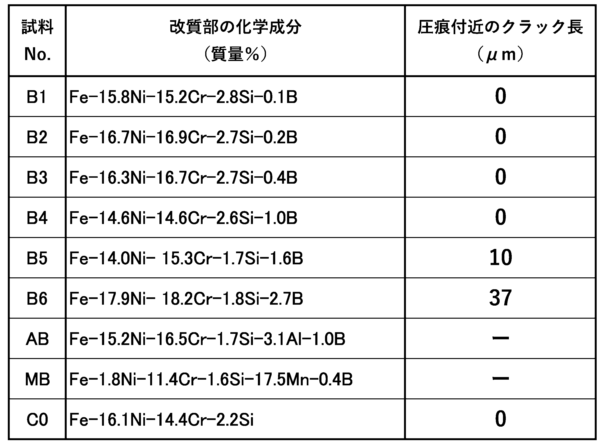
各試料の改質域から欠陥(引け巣、割れ等)がない部分(改質部)を選択して、その略中央付近の化学成分を分析した。その結果を表2に併せて示した。元素記号の前に付した数値が、分析部分(改質部)の全体に対する質量%を示す。
各試料の改質域から欠陥(引け巣、割れ等)がない部分(改質部)を選択して、その略中央付近の化学成分を分析した。その結果を表2に併せて示した。元素記号の前に付した数値が、分析部分(改質部)の全体に対する質量%を示す。
成分分析は次のように行なった。BはEPMA(株式会社島津製作所製EPMA-8050G)により分析した。その他の元素は、EDS(Oxford Instruments社製X-MAXN)により分析される。それぞれの具体的な分析条件は次の通りである。欠陥がない改質域から切り出した分析部分(改質部)を樹脂埋め後に断面を研磨した分析用の試料(φ25mm)を製作した。Bは、その試料中央面(100μm×100μm)でEPMAによりマップ分析を行った。他の成分は、その試料中央面(1000μm×300μm)で、EDS(電圧:15kV、電流:12A)によりマップ分析を行った。また、その試料中にオーステナイト相が含まれることはXRDにより確認した。
《圧痕試験》
各試料の改質域の脆性を圧痕試験により評価した。圧痕試験は、ビッカース硬さ試験(JIS Z2244)を参考にしつつ、ダイヤモンド製の四角錐(圧子)を改質域へ押し付けて行なった。このときの試験荷重は100gfとした。
各試料の改質域の脆性を圧痕試験により評価した。圧痕試験は、ビッカース硬さ試験(JIS Z2244)を参考にしつつ、ダイヤモンド製の四角錐(圧子)を改質域へ押し付けて行なった。このときの試験荷重は100gfとした。
一部の試料について、改質域にできた圧痕を光学顕微鏡で観察した写真を図7に例示した。図7からもわかるように、クラックは、圧痕の角を起点にして、略直線状に短く延びていた。各試料の改質域毎に、異なる三箇所でクラックの長さ(クラックが複数あるときは合計値)を直線近似して測定した。それらの平均値(N=3)を、改質域一つあたりのクラック長とした。こうして求めた各試料のクラック長を表2に併せて示した。
《評価》
(1)図6から明らかなように、改質部(改質材、改質域)に適量のBが含まれるとき、引け巣やクラックが縮小さらには出現しない(消失する)ことがわかった。この傾向は、Bと共にAlを含むときに顕著であった。また、NiがMnで置換されても、引け巣やクラックの発生が十分に抑止されることもわかった。
(1)図6から明らかなように、改質部(改質材、改質域)に適量のBが含まれるとき、引け巣やクラックが縮小さらには出現しない(消失する)ことがわかった。この傾向は、Bと共にAlを含むときに顕著であった。また、NiがMnで置換されても、引け巣やクラックの発生が十分に抑止されることもわかった。
(2)表2からわかるように、改質部に含まれるBが過多(例えば1.5%超)になると、圧痕周りにクラックが発生した。また、そのB量の増加と共にクラックも増大することもわかった。
以上から、本発明によれば、改質域に現れる欠陥を縮小さらには消失させれることが確認された。これにより、改質部の形成自由度の拡大、ケイ素鋼板の有効活用または改質工程の効率化等を図りつつ、改質部を有する電磁鋼板を製造できることが明らかとなった。また改質域に含まれるB量の調整により、改質部付近の割れ抑止や強度確保または電磁鋼板の積層性や歩留りの向上等を図れることもわかった。

M ケイ素鋼板
1 ロータコアシート
2 ステータコアシート
101 スロット
111 ブリッジ
121 改質部
311 改質材
1 ロータコアシート
2 ステータコアシート
101 スロット
111 ブリッジ
121 改質部
311 改質材
Claims (14)
- 少なくともオーステナイト相を含む改質部を、一部に有するケイ素鋼板からなり、
該改質部全体に対してBが0.15~3質量%含まれる電磁鋼板。 - 前記改質部は、少なくともNi、Cr、Siをさらに含む鉄合金からなる請求項1に記載の電磁鋼板。
- 前記鉄合金は、さらにAlおよび/またはMnを含む請求項2に記載の電磁鋼板。
- 前記改質部は、前記オーステナイト相と化合物相を含む金属組織を有し、
該化合物相は、Bを含むB系化合物を含み、
該B系化合物は、該オーステナイト相よりも低密度である請求項1に記載の電磁鋼板。 - 前記金属組織は、初晶オーステナイト相と共晶を含み、
前記B系化合物は、該共晶に含まれる請求項4に記載の電磁鋼板。 - 前記B系化合物は、前記金属組織全体に対する体積割合で1~45%含まれる請求項4に記載の電磁鋼板。
- 前記B系化合物は、(Fe、Cr)2B、Fe2B、Cr2B、Cr5B3 およびCrBの一種以上を含む請求項4に記載の電磁鋼板。
- 前記B系化合物は、少なくとも二種以上の化合物が交互に形成された複化合物を含む請求項4に記載の電磁鋼板。
- 前記複化合物は、積層状である請求項8に記載の電磁鋼板。
- 前記複化合物は、Fe2B層とCr2B層が交互に積層されてなる請求項9に記載の電磁鋼板。
- 前記オーステナイト相は、Niおよび/またはCrを含む請求項1または4に記載の電磁鋼板。
- 前記改質部がロータコアのブリッジとなる領域の少なくとも一部に形成されるコアシートに用いられる請求項1に記載の電磁鋼板。
- ケイ素鋼板の特定領域上に配置した改質材へ高エネルギービームを照射して、少なくともオーステナイト相を含む改質部を該ケイ素鋼板の一部に形成する改質工程を備え、
該改質部全体に対してBが0.15~3質量%含まれる電磁鋼板の製造方法。 - 前記改質部全体に対してBが0.3~1.5質量%含まれる請求項13に記載の電磁鋼板の製造方法。
Applications Claiming Priority (8)
| Application Number | Priority Date | Filing Date | Title |
|---|---|---|---|
| JP2023023038 | 2023-02-17 | ||
| JP2023023033 | 2023-02-17 | ||
| JP2023-023038 | 2023-02-17 | ||
| JP2023-023033 | 2023-02-17 | ||
| JP2023-136916 | 2023-08-25 | ||
| JP2023136916A JP2024117688A (ja) | 2023-02-17 | 2023-08-25 | 電磁鋼板とその製造方法、コアシート、ロータおよび電動機 |
| JP2023-136918 | 2023-08-25 | ||
| JP2023136918A JP2024117689A (ja) | 2023-02-17 | 2023-08-25 | 電磁鋼板とその製造方法およびロータコア |
Publications (1)
| Publication Number | Publication Date |
|---|---|
| WO2024172000A1 true WO2024172000A1 (ja) | 2024-08-22 |
Family
ID=92421901
Family Applications (1)
| Application Number | Title | Priority Date | Filing Date |
|---|---|---|---|
| PCT/JP2024/004695 Ceased WO2024172000A1 (ja) | 2023-02-17 | 2024-02-12 | 電磁鋼板およびその製造方法 |
Country Status (1)
| Country | Link |
|---|---|
| WO (1) | WO2024172000A1 (ja) |
Citations (4)
| Publication number | Priority date | Publication date | Assignee | Title |
|---|---|---|---|---|
| JP2008099360A (ja) * | 2006-10-06 | 2008-04-24 | Toyota Motor Corp | 鋼材の非磁性領域形成方法及び非磁性領域が形成された鋼材 |
| JP2008308712A (ja) * | 2007-06-13 | 2008-12-25 | Toyota Motor Corp | 鋼材の非磁性領域形成方法及び非磁性領域が形成された鋼材 |
| JP2011006741A (ja) * | 2009-06-25 | 2011-01-13 | Denso Corp | 鋼材の磁気特性改質領域の形成方法 |
| US20180278100A1 (en) * | 2017-03-27 | 2018-09-27 | Ford Global Technologies, Llc | Method for adjusting magnetic permeability of electrical steel |
-
2024
- 2024-02-12 WO PCT/JP2024/004695 patent/WO2024172000A1/ja not_active Ceased
Patent Citations (4)
| Publication number | Priority date | Publication date | Assignee | Title |
|---|---|---|---|---|
| JP2008099360A (ja) * | 2006-10-06 | 2008-04-24 | Toyota Motor Corp | 鋼材の非磁性領域形成方法及び非磁性領域が形成された鋼材 |
| JP2008308712A (ja) * | 2007-06-13 | 2008-12-25 | Toyota Motor Corp | 鋼材の非磁性領域形成方法及び非磁性領域が形成された鋼材 |
| JP2011006741A (ja) * | 2009-06-25 | 2011-01-13 | Denso Corp | 鋼材の磁気特性改質領域の形成方法 |
| US20180278100A1 (en) * | 2017-03-27 | 2018-09-27 | Ford Global Technologies, Llc | Method for adjusting magnetic permeability of electrical steel |
Similar Documents
| Publication | Publication Date | Title |
|---|---|---|
| JP3690616B2 (ja) | 回転機 | |
| JP5699642B2 (ja) | モータコア | |
| Garibaldi | Laser additive manufacturing of soft magnetic cores for rotating electrical machinery: materials development and part design | |
| JP6514752B2 (ja) | Fe系非晶質軟磁性バルク合金、その製造方法、およびその使用 | |
| CN111373494A (zh) | 高磁导率软磁合金和制造高磁导率软磁合金的方法 | |
| JP7783485B2 (ja) | 磁性部材の製造方法 | |
| Andreiev et al. | Soft-magnetic behavior of laser beam melted FeSi3 alloy with graded cross-section | |
| Hamada et al. | Development of rotor core with high magnetic flux by partial non-magnetic improvement of silicon steel | |
| Genç et al. | Influence of heat treatment on microstructure and magnetic properties of laser powder bed fusion generated NdFeB magnets | |
| KR20230123512A (ko) | 회전 전기 기기, 스테이터의 철심 및 로터의 철심의세트, 회전 전기 기기의 제조 방법, 스테이터용 무방향성 전자 강판 및 로터용 무방향성 전자 강판의 제조 방법, 스테이터 및 로터의 제조 방법, 그리고 무방향성 전자 강판의 세트 | |
| Lee et al. | Enhanced magnetic properties and Goss texture development of FeSi3. 5 by direct energy deposition | |
| US11827961B2 (en) | FeCoV alloy and method for producing a strip from an FeCoV alloy | |
| JP2024117689A (ja) | 電磁鋼板とその製造方法およびロータコア | |
| JP2024117688A (ja) | 電磁鋼板とその製造方法、コアシート、ロータおよび電動機 | |
| CA3184065A1 (en) | A method for the additive manufacture of magnetic materials | |
| WO2024171622A1 (ja) | 電磁鋼板とその製造方法およびロータコア | |
| JP2024117128A (ja) | 電磁鋼板とその製造方法、コアシート、ロータおよび電動機 | |
| WO2024171623A1 (ja) | 電磁鋼板とその製造方法、コアシート、ロータコア、ロータおよび電動機 | |
| Hamada et al. | Development of Partial Non-Magnetization Improvement for Silicon Steel and Rotor Evaluation | |
| CN1081404C (zh) | 永磁场型旋转电机 | |
| Gargalis | Optimisation of silicon content in Fe-Si alloys processed via laser powder bed fusion for an additively manufactured soft magnetic core | |
| JP5561148B2 (ja) | 圧縮応力下での鉄損劣化の小さいモータコア | |
| Tiismus et al. | Axial Synchronous Magnetic Coupling Modeling and Printing with Selective Laser Melting | |
| WO2023228821A1 (ja) | 発電用磁歪素子および磁歪発電デバイス | |
| Urban et al. | Correlation between residual stress, building angle and illumination parameters of additive manufactured FeSi6. 5 and mechanical and magnetic properties |
Legal Events
| Date | Code | Title | Description |
|---|---|---|---|
| 121 | Ep: the epo has been informed by wipo that ep was designated in this application |
Ref document number: 24756845 Country of ref document: EP Kind code of ref document: A1 |
|
| NENP | Non-entry into the national phase |
Ref country code: DE |
|
| 122 | Ep: pct application non-entry in european phase |
Ref document number: 24756845 Country of ref document: EP Kind code of ref document: A1 |