WO2024171714A1 - プラズマ処理装置 - Google Patents
プラズマ処理装置 Download PDFInfo
- Publication number
- WO2024171714A1 WO2024171714A1 PCT/JP2024/001413 JP2024001413W WO2024171714A1 WO 2024171714 A1 WO2024171714 A1 WO 2024171714A1 JP 2024001413 W JP2024001413 W JP 2024001413W WO 2024171714 A1 WO2024171714 A1 WO 2024171714A1
- Authority
- WO
- WIPO (PCT)
- Prior art keywords
- ring
- voltage level
- substrate
- bias electrode
- electrode
- Prior art date
- Legal status (The legal status is an assumption and is not a legal conclusion. Google has not performed a legal analysis and makes no representation as to the accuracy of the status listed.)
- Ceased
Links
Images






Classifications
-
- H—ELECTRICITY
- H01—ELECTRIC ELEMENTS
- H01J—ELECTRIC DISCHARGE TUBES OR DISCHARGE LAMPS
- H01J37/00—Discharge tubes with provision for introducing objects or material to be exposed to the discharge, e.g. for the purpose of examination or processing thereof
- H01J37/32—Gas-filled discharge tubes
- H01J37/32009—Arrangements for generation of plasma specially adapted for examination or treatment of objects, e.g. plasma sources
- H01J37/32082—Radio frequency generated discharge
- H01J37/32137—Radio frequency generated discharge controlling of the discharge by modulation of energy
- H01J37/32146—Amplitude modulation, includes pulsing
-
- H—ELECTRICITY
- H01—ELECTRIC ELEMENTS
- H01J—ELECTRIC DISCHARGE TUBES OR DISCHARGE LAMPS
- H01J37/00—Discharge tubes with provision for introducing objects or material to be exposed to the discharge, e.g. for the purpose of examination or processing thereof
- H01J37/32—Gas-filled discharge tubes
- H01J37/32009—Arrangements for generation of plasma specially adapted for examination or treatment of objects, e.g. plasma sources
- H01J37/32082—Radio frequency generated discharge
- H01J37/32174—Circuits specially adapted for controlling the RF discharge
-
- H—ELECTRICITY
- H01—ELECTRIC ELEMENTS
- H01J—ELECTRIC DISCHARGE TUBES OR DISCHARGE LAMPS
- H01J37/00—Discharge tubes with provision for introducing objects or material to be exposed to the discharge, e.g. for the purpose of examination or processing thereof
- H01J37/32—Gas-filled discharge tubes
- H01J37/32431—Constructional details of the reactor
- H01J37/32532—Electrodes
- H01J37/32541—Shape
-
- H—ELECTRICITY
- H01—ELECTRIC ELEMENTS
- H01J—ELECTRIC DISCHARGE TUBES OR DISCHARGE LAMPS
- H01J37/00—Discharge tubes with provision for introducing objects or material to be exposed to the discharge, e.g. for the purpose of examination or processing thereof
- H01J37/32—Gas-filled discharge tubes
- H01J37/32431—Constructional details of the reactor
- H01J37/32532—Electrodes
- H01J37/32568—Relative arrangement or disposition of electrodes; moving means
-
- H—ELECTRICITY
- H01—ELECTRIC ELEMENTS
- H01J—ELECTRIC DISCHARGE TUBES OR DISCHARGE LAMPS
- H01J37/00—Discharge tubes with provision for introducing objects or material to be exposed to the discharge, e.g. for the purpose of examination or processing thereof
- H01J37/32—Gas-filled discharge tubes
- H01J37/32431—Constructional details of the reactor
- H01J37/32532—Electrodes
- H01J37/32577—Electrical connecting means
-
- H—ELECTRICITY
- H01—ELECTRIC ELEMENTS
- H01J—ELECTRIC DISCHARGE TUBES OR DISCHARGE LAMPS
- H01J37/00—Discharge tubes with provision for introducing objects or material to be exposed to the discharge, e.g. for the purpose of examination or processing thereof
- H01J37/32—Gas-filled discharge tubes
- H01J37/32431—Constructional details of the reactor
- H01J37/32623—Mechanical discharge control means
- H01J37/32642—Focus rings
-
- H—ELECTRICITY
- H01—ELECTRIC ELEMENTS
- H01J—ELECTRIC DISCHARGE TUBES OR DISCHARGE LAMPS
- H01J37/00—Discharge tubes with provision for introducing objects or material to be exposed to the discharge, e.g. for the purpose of examination or processing thereof
- H01J37/32—Gas-filled discharge tubes
- H01J37/32431—Constructional details of the reactor
- H01J37/32697—Electrostatic control
-
- H—ELECTRICITY
- H01—ELECTRIC ELEMENTS
- H01J—ELECTRIC DISCHARGE TUBES OR DISCHARGE LAMPS
- H01J37/00—Discharge tubes with provision for introducing objects or material to be exposed to the discharge, e.g. for the purpose of examination or processing thereof
- H01J37/32—Gas-filled discharge tubes
- H01J37/32431—Constructional details of the reactor
- H01J37/32715—Workpiece holder
-
- H—ELECTRICITY
- H05—ELECTRIC TECHNIQUES NOT OTHERWISE PROVIDED FOR
- H05H—PLASMA TECHNIQUE; PRODUCTION OF ACCELERATED ELECTRICALLY-CHARGED PARTICLES OR OF NEUTRONS; PRODUCTION OR ACCELERATION OF NEUTRAL MOLECULAR OR ATOMIC BEAMS
- H05H1/00—Generating plasma; Handling plasma
- H05H1/24—Generating plasma
- H05H1/46—Generating plasma using applied electromagnetic fields, e.g. high frequency or microwave energy
-
- H—ELECTRICITY
- H10—SEMICONDUCTOR DEVICES; ELECTRIC SOLID-STATE DEVICES NOT OTHERWISE PROVIDED FOR
- H10P—GENERIC PROCESSES OR APPARATUS FOR THE MANUFACTURE OR TREATMENT OF DEVICES COVERED BY CLASS H10
- H10P50/00—Etching of wafers, substrates or parts of devices
- H10P50/20—Dry etching; Plasma etching; Reactive-ion etching
- H10P50/24—Dry etching; Plasma etching; Reactive-ion etching of semiconductor materials
- H10P50/242—Dry etching; Plasma etching; Reactive-ion etching of semiconductor materials of Group IV materials
-
- H—ELECTRICITY
- H10—SEMICONDUCTOR DEVICES; ELECTRIC SOLID-STATE DEVICES NOT OTHERWISE PROVIDED FOR
- H10P—GENERIC PROCESSES OR APPARATUS FOR THE MANUFACTURE OR TREATMENT OF DEVICES COVERED BY CLASS H10
- H10P72/00—Handling or holding of wafers, substrates or devices during manufacture or treatment thereof
- H10P72/70—Handling or holding of wafers, substrates or devices during manufacture or treatment thereof for supporting or gripping
- H10P72/72—Handling or holding of wafers, substrates or devices during manufacture or treatment thereof for supporting or gripping using electrostatic chucks
- H10P72/722—Details of electrostatic chucks
-
- H—ELECTRICITY
- H01—ELECTRIC ELEMENTS
- H01J—ELECTRIC DISCHARGE TUBES OR DISCHARGE LAMPS
- H01J2237/00—Discharge tubes exposing object to beam, e.g. for analysis treatment, etching, imaging
- H01J2237/32—Processing objects by plasma generation
- H01J2237/33—Processing objects by plasma generation characterised by the type of processing
- H01J2237/334—Etching
- H01J2237/3343—Problems associated with etching
- H01J2237/3344—Problems associated with etching isotropy
Definitions
- An exemplary embodiment of the present disclosure relates to a plasma processing apparatus.
- Patent Document 1 a technology for supplying high frequency and pulse voltage to multiple electrodes is described in Patent Document 1.
- This disclosure provides technology that can improve the in-plane uniformity of a substrate during plasma processing.
- a plasma processing apparatus includes a plasma processing chamber and a substrate support disposed within the plasma processing chamber, the substrate support including a base, an electrostatic chuck disposed on the base and having a substrate support surface and a ring support surface, and at least one annular member disposed on the ring support surface to surround a substrate disposed on the substrate support surface, a substrate chuck electrode disposed below the substrate support surface within the electrostatic chuck, at least one ring chuck electrode disposed below the ring support surface within the electrostatic chuck, a substrate bias electrode disposed within the electrostatic chuck and below the substrate chuck electrode, and at least one ring chuck electrode disposed within the electrostatic chuck and below the substrate chuck electrode.
- the switch includes a ring bias electrode disposed below the pole, a first voltage pulse generator configured to generate a first sequence of voltage pulses having a first voltage level, a second voltage pulse generator configured to generate a second sequence of voltage pulses having a second voltage level, and a switch configured to switch between a first connection state and a second connection state, the first connection state being a state in which the first voltage pulse generator is electrically connected to the substrate bias electrode and the second voltage pulse generator is electrically connected to the ring bias electrode, and the second connection state being a state in which the first voltage pulse generator is electrically connected to the ring bias electrode and the second voltage pulse generator is electrically connected to the substrate bias electrode.
- One exemplary embodiment of the present disclosure provides a technology that can improve the in-plane uniformity of a substrate during plasma processing.
- FIG. 1 is a diagram for explaining a configuration example of a plasma processing system.
- FIG. 1 is a diagram for explaining a configuration example of a capacitively coupled plasma processing apparatus.
- 3A to 3C are diagrams for explaining a configuration example of a substrate support part and a DC power supply in the first exemplary embodiment.
- 1A and 1B are diagrams for explaining examples of the configuration of bias electrodes in a plan view.
- FIG. 4 is a diagram showing an example of a voltage pulse.
- FIG. 2 is a diagram for explaining a configuration example of a switch;
- FIG. 13 is a diagram for explaining the fluctuation of a plasma sheath above a substrate.
- FIG. 13 is a diagram for explaining the fluctuation of a plasma sheath above a substrate.
- FIG. 13 is a diagram for explaining the fluctuation of the plasma sheath above the substrate when the thickness of the ring assembly is large.
- FIG. 13 is a diagram for explaining the variation of the plasma sheath on the substrate when the thickness of the ring assembly is reduced.
- FIG. 13A and 13B are diagrams for explaining other examples of the arrangement of ring bias electrodes.
- 13A and 13B are diagrams for explaining other examples of the arrangement of ring bias electrodes.
- 13A and 13B are diagrams for explaining a configuration example of a substrate support part and a DC power supply in a second exemplary embodiment.
- 13A and 13B are diagrams for explaining a configuration example of a substrate support part and a DC power supply in a second exemplary embodiment.
- a plasma processing chamber and a substrate support disposed within the plasma processing chamber including a base, an electrostatic chuck disposed on the base and having a substrate support surface and a ring support surface, and at least one annular member disposed on the ring support surface to surround a substrate disposed on the substrate support surface, a substrate chuck electrode disposed within the electrostatic chuck below the substrate support surface, at least one ring chuck electrode disposed within the electrostatic chuck below the ring support surface, a substrate bias electrode disposed within the electrostatic chuck and below the substrate chuck electrode, and a ring bias electrode disposed within the electrostatic chuck and below the at least one ring chuck electrode.
- a plasma processing apparatus includes a bias electrode, a first voltage pulse generator configured to generate a sequence of first voltage pulses having a first voltage level, a second voltage pulse generator configured to generate a sequence of second voltage pulses having a second voltage level, and a switch configured to switch between a first connection state and a second connection state, the first connection state being a state in which the first voltage pulse generator is electrically connected to the substrate bias electrode and the second voltage pulse generator is electrically connected to the ring bias electrode, and the second connection state being a state in which the first voltage pulse generator is electrically connected to the ring bias electrode and the second voltage pulse generator is electrically connected to the substrate bias electrode.
- the switch includes a rotatable member, a first wire and a second wire attached to the rotatable member, and is configured to switch between a first connection state and a second connection state by rotation of the rotatable member, the first connection state being a state in which the first voltage pulse generator is electrically connected to the substrate bias electrode via the first wire and the second voltage pulse generator is electrically connected to the ring bias electrode via the second wire, and the second connection state being a state in which the first voltage pulse generator is electrically connected to the ring bias electrode via the first wire and the second voltage pulse generator is electrically connected to the substrate bias electrode via the second wire.
- the switch is an electrical circuit.
- the first voltage level and the second voltage level have negative polarity.
- the absolute value of the first voltage level is greater than the absolute value of the second voltage level.
- the substrate bias electrode and the ring bias electrode are positioned at the same height.
- the substrate bias electrode and the ring bias electrode are positioned at different heights.
- the ring bias electrode is positioned lower than the substrate bias electrode.
- the substrate bias electrode has an outer edge region and the ring bias electrode has an inner edge region that vertically overlaps with the outer edge region of the substrate bias electrode.
- the ring chuck electrodes include an inner ring chuck electrode to which a first ring chuck voltage having a first polarity is applied, and an outer ring chuck electrode to which a second ring chuck voltage having a second polarity is applied.
- a plasma processing chamber and a substrate support disposed within the plasma processing chamber including a base, an electrostatic chuck disposed on the base and having a substrate support surface and a ring support surface, and at least one annular member disposed on the ring support surface to surround a substrate disposed on the substrate support surface, a substrate chuck electrode disposed below the substrate support surface within the electrostatic chuck, at least one ring chuck electrode disposed below the ring support surface within the electrostatic chuck, and a substrate support disposed within the electrostatic chuck.
- a substrate bias electrode disposed below the substrate chuck electrode; a ring bias electrode disposed within the electrostatic chuck and disposed below the at least one ring chuck electrode; a first DC power supply configured to generate a first primary DC signal having a first primary voltage level; a second DC power supply configured to generate a second primary DC signal having a second primary voltage level; and a second DC power supply configured to generate a first secondary DC signal having a first secondary voltage level and a second secondary DC signal having a second secondary voltage level from the first primary DC signal and the second primary DC signal.
- a plasma processing apparatus including: a voltage adder configured to generate a second secondary DC signal such that a second secondary voltage level has the same voltage level as the first primary voltage level; a first voltage pulse generator configured to generate a sequence of first voltage pulses having the first secondary voltage level from the first secondary DC signal; and a second voltage pulse generator configured to generate a sequence of second voltage pulses having the second secondary voltage level from the second secondary DC signal.
- the first primary voltage level and the second primary voltage level have negative polarity.
- the absolute value of the first primary voltage level is greater than the absolute value of the second primary voltage level.
- the absolute value of the first primary voltage level is greater than or equal to five times the absolute value of the second primary voltage level.
- the substrate bias electrode and the ring bias electrode are positioned at the same height.
- the substrate bias electrode and the ring bias electrode are positioned at different heights.
- the ring bias electrode is positioned lower than the substrate bias electrode.
- the substrate bias electrode has an outer edge region and the ring bias electrode has an inner edge region that vertically overlaps with the outer edge region of the substrate bias electrode.
- the ring chuck electrodes include an inner ring chuck electrode to which a first ring chuck voltage having a first polarity is applied, and an outer ring chuck electrode to which a second ring chuck voltage having a second polarity is applied.
- FIG. 1 is a diagram for explaining a configuration example of a plasma processing system.
- the plasma processing system includes a plasma processing device 1 and a control unit 2.
- the plasma processing system is an example of a substrate processing system
- the plasma processing device 1 is an example of a substrate processing device.
- the plasma processing device 1 includes a plasma processing chamber 10, a substrate support unit 11, and a plasma generation unit 12.
- the plasma processing chamber 10 has a plasma processing space.
- the plasma processing chamber 10 also has at least one gas supply port for supplying at least one processing gas to the plasma processing space, and at least one gas exhaust port for exhausting gas from the plasma processing space.
- the gas supply port is connected to a gas supply unit 20 described later, and the gas exhaust port is connected to an exhaust system 40 described later.
- the substrate support unit 11 is disposed in the plasma processing space, and has a substrate support surface for supporting a substrate.
- the plasma generating unit 12 is configured to generate plasma from at least one processing gas supplied into the plasma processing space.
- the plasma formed in the plasma processing space may be capacitively coupled plasma (CCP), inductively coupled plasma (ICP), ECR plasma (Electron-Cyclotron-resonance plasma), Helicon wave excited plasma (HWP), or surface wave plasma (SWP), etc.
- various types of plasma generating units may be used, including AC (Alternating Current) plasma generating units and DC (Direct Current) plasma generating units.
- the AC signal (AC power) used in the AC plasma generating unit has a frequency in the range of 100 kHz to 10 GHz.
- AC signals include RF (Radio Frequency) signals and microwave signals.
- the RF signal has a frequency in the range of 100 kHz to 150 MHz.
- the control unit 2 processes computer-executable instructions that cause the plasma processing apparatus 1 to perform the various steps described in this disclosure.
- the control unit 2 may be configured to control each element of the plasma processing apparatus 1 to perform the various steps described herein. In one embodiment, a part or all of the control unit 2 may be included in the plasma processing apparatus 1.
- the control unit 2 may include, for example, a computer 2a.
- the computer 2a may include, for example, a processing unit (CPU: Central Processing Unit) 2a1, a storage unit 2a2, and a communication interface 2a3.
- the processing unit 2a1 may be configured to perform various control operations by reading a program from the storage unit 2a2 and executing the read program. This program may be stored in the storage unit 2a2 in advance, or may be acquired via a medium when necessary.
- the acquired program is stored in the storage unit 2a2, and is read from the storage unit 2a2 by the processing unit 2a1 and executed.
- the medium may be various storage media readable by the computer 2a, or may be a communication line connected to the communication interface 2a3.
- the memory unit 2a2 may include a RAM (Random Access Memory), a ROM (Read Only Memory), a HDD (Hard Disk Drive), a SSD (Solid State Drive), or a combination of these.
- the communication interface 2a3 may communicate with the plasma processing device 1 via a communication line such as a LAN (Local Area Network).
- FIG. 1 is a diagram for explaining a configuration example of a capacitively coupled plasma processing device.
- the capacitively coupled plasma processing apparatus 1 includes a plasma processing chamber 10, a gas supply unit 20, a power supply 30, and an exhaust system 40.
- the plasma processing apparatus 1 also includes a substrate support unit 11 and a gas inlet unit.
- the gas inlet unit is configured to introduce at least one processing gas into the plasma processing chamber 10.
- the gas inlet unit includes a shower head 13.
- the substrate support unit 11 is disposed in the plasma processing chamber 10.
- the shower head 13 is disposed above the substrate support unit 11. In one embodiment, the shower head 13 constitutes at least a part of the ceiling of the plasma processing chamber 10.
- the plasma processing chamber 10 has a plasma processing space 10s defined by the shower head 13, the sidewall 10a of the plasma processing chamber 10, and the substrate support unit 11.
- the plasma processing chamber 10 is grounded.
- the shower head 13 and the substrate support unit 11 are electrically insulated from the plasma processing chamber 10 housing.
- the substrate support 11 includes a main body 111 and a ring assembly (edge ring assembly) 112.
- the main body 111 has a central region 111a for supporting the substrate W and an annular region 111b for supporting the ring assembly 112.
- a wafer is an example of a substrate W.
- the annular region 111b of the main body 111 surrounds the central region 111a of the main body 111 in a plan view.
- the substrate W is disposed on the central region 111a of the main body 111, and the ring assembly 112 is disposed on the annular region 111b of the main body 111 so as to surround the substrate W on the central region 111a of the main body 111. Therefore, the central region 111a is also called a substrate support surface for supporting the substrate W, and the annular region 111b is also called a ring support surface for supporting the ring assembly 112.
- the main body 111 includes a base 1110 and an electrostatic chuck 1111.
- the base 1110 includes a conductive member.
- the conductive member of the base 1110 may function as a lower electrode.
- the electrostatic chuck 1111 is disposed on the base 1110.
- the electrostatic chuck 1111 includes a ceramic member 1111a and an electrostatic electrode 1111b disposed within the ceramic member 1111a.
- the ceramic member 1111a has a central region 111a. In one embodiment, the ceramic member 1111a also has an annular region 111b. Note that other members surrounding the electrostatic chuck 1111, such as an annular electrostatic chuck or an annular insulating member, may have the annular region 111b.
- the ring assembly 112 may be disposed on the annular electrostatic chuck or the annular insulating member, or may be disposed on both the electrostatic chuck 1111 and the annular insulating member.
- an RF or DC electrode may be disposed within the ceramic member 1111a, in which case the RF or DC electrode functions as the lower electrode.
- the RF or DC electrode is also called a bias electrode. Note that both the conductive member of the base 1110 and the RF or DC electrode may function as two lower electrodes.
- the ring assembly 112 includes one or more annular members.
- the one or more annular members include one or more edge rings and at least one cover ring.
- the edge rings are formed of a conductive or insulating material, and the cover rings are formed of an insulating material.
- the substrate support 11 may also include a temperature adjustment module configured to adjust at least one of the electrostatic chuck 1111, the ring assembly 112, and the substrate to a target temperature.
- the temperature adjustment module may include a heater, a heat transfer medium, a flow passage 1110a, or a combination thereof.
- a heat transfer fluid such as brine or a gas flows through the flow passage 1110a.
- the flow passage 1110a is formed in the base 1110, and one or more heaters are disposed in the ceramic member 1111a of the electrostatic chuck 1111.
- the substrate support 11 may also include a heat transfer gas supply configured to supply a heat transfer gas between the back surface of the substrate W and the central region 111a.
- the shower head 13 is configured to introduce at least one processing gas from the gas supply unit 20 into the plasma processing space 10s.
- the shower head 13 has at least one gas supply port 13a, at least one gas diffusion chamber 13b, and multiple gas inlets 13c.
- the processing gas supplied to the gas supply port 13a passes through the gas diffusion chamber 13b and is introduced into the plasma processing space 10s from the multiple gas inlets 13c.
- the shower head 13 also includes an upper electrode.
- the gas introduction unit may include, in addition to the shower head 13, one or more side gas injectors (SGI) attached to one or more openings formed in the side wall 10a.
- SGI side gas injectors
- the gas supply unit 20 may include at least one gas source 21 and at least one flow controller 22.
- the gas supply unit 20 is configured to supply at least one process gas from a respective gas source 21 through a respective flow controller 22 to the showerhead 13.
- Each flow controller 22 may include, for example, a mass flow controller or a pressure-controlled flow controller.
- the gas supply unit 20 may include at least one flow modulation device that modulates or pulses the flow rate of the at least one process gas.
- the power supply 30 includes an RF power supply 31 coupled to the plasma processing chamber 10 via at least one impedance matching circuit.
- the RF power supply 31 is configured to supply at least one RF signal (RF power), such as a source RF signal and a bias RF signal, to at least one lower electrode and/or at least one upper electrode. This causes a plasma to be formed from at least one processing gas supplied to the plasma processing space 10s.
- the RF power supply 31 can function as at least a part of the plasma generating unit 12.
- a bias RF signal to at least one lower electrode, a bias potential is generated on the substrate W, and ion components in the formed plasma can be attracted to the substrate W.
- the RF power supply 31 includes a first RF generating unit 31a and a second RF generating unit 31b.
- the first RF generating unit 31a is coupled to at least one lower electrode and/or at least one upper electrode via at least one impedance matching circuit and configured to generate a source RF signal (source RF power) for plasma generation.
- the source RF signal has a frequency in the range of 10 MHz to 150 MHz.
- the first RF generating unit 31a may be configured to generate multiple source RF signals having different frequencies. The generated one or more source RF signals are supplied to at least one lower electrode and/or at least one upper electrode.
- the second RF generator 31b is coupled to at least one lower electrode via at least one impedance matching circuit and configured to generate a bias RF signal (bias RF power).
- the frequency of the bias RF signal may be the same as or different from the frequency of the source RF signal.
- the bias RF signal has a frequency lower than the frequency of the source RF signal.
- the bias RF signal has a frequency in the range of 100 kHz to 60 MHz.
- the second RF generator 31b may be configured to generate multiple bias RF signals having different frequencies.
- the generated one or more bias RF signals are provided to at least one lower electrode. Also, in various embodiments, at least one of the source RF signal and the bias RF signal may be pulsed.
- the power supply 30 may also include a DC power supply 32 coupled to the plasma processing chamber 10.
- the DC power supply 32 includes a first DC generator 32a and a second DC generator 32b.
- the first DC generator 32a is connected to at least one lower electrode and configured to generate a first DC signal.
- the generated first DC signal is applied to the at least one lower electrode.
- the second DC generator 32b is connected to at least one upper electrode and configured to generate a second DC signal.
- the generated second DC signal is applied to the at least one upper electrode.
- the first and second DC signals may be pulsed.
- a sequence of DC-based voltage pulses is applied to at least one lower electrode and/or at least one upper electrode.
- the voltage pulses may have a rectangular, trapezoidal, triangular or combination of these pulse waveforms.
- a waveform generator for generating a sequence of voltage pulses from the DC signal is connected between the first DC generator 32a and at least one lower electrode.
- the first DC generator 32a and the waveform generator constitute a voltage pulse generator.
- the second DC generator 32b and the waveform generator constitute a voltage pulse generator
- the voltage pulse generator is connected to at least one upper electrode.
- the voltage pulses may have a positive polarity or a negative polarity.
- the sequence of voltage pulses may include one or more positive polarity voltage pulses and one or more negative polarity voltage pulses within one period.
- the first and second DC generating units 32a and 32b may be provided in addition to the RF power source 31, or the first DC generating unit 32a may be provided in place of the second RF generating unit 31b.
- the exhaust system 40 may be connected to, for example, a gas exhaust port 10e provided at the bottom of the plasma processing chamber 10.
- the exhaust system 40 may include a pressure regulating valve and a vacuum pump. The pressure in the plasma processing space 10s is adjusted by the pressure regulating valve.
- the vacuum pump may include a turbomolecular pump, a dry pump, or a combination thereof.
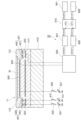
- Fig. 3 is a diagram for explaining a configuration example of the substrate support part 11 and the DC power supply 32 in the first exemplary embodiment.
- the substrate support part 11 has a substrate chuck electrode 200, a ring chuck electrode 201, a substrate bias electrode 202, and a ring bias electrode 203 inside the electrostatic chuck 1111.
- the substrate chuck electrode 200 and the ring chuck electrode 201 may be an example of the electrostatic electrode 1111b.
- the DC power supply 32 includes a first DC power supply 250, a second DC power supply 251, a first voltage pulse generator 260, a second voltage pulse generator 261, an impedance matcher 270, and a switch 280.
- the substrate chuck electrode 200 can be disposed below the substrate support surface within the electrostatic chuck 1111.
- the substrate chuck electrode 200 has a circular shape.
- the substrate chuck electrode 200 is connected to a direct current (DC) power supply 301 via a switch 300.
- DC direct current
- a DC voltage from the DC power supply 301 is applied to the substrate chuck electrode 200, an electrostatic force of attraction (Coulomb force) is generated between the substrate chuck electrode 200 and the substrate W.
- the substrate W is attracted to the electrostatic chuck 1111 by the electrostatic force and is adsorbed and held on the substrate support surface.
- the ring chuck electrode 201 may be disposed below the ring support surface within the electrostatic chuck 1111.
- the ring chuck electrode 201 includes an inner ring chuck electrode 400 and an outer ring chuck electrode 401.
- the inner ring chuck electrode 400 is connected to a DC power supply 411 via a switch 410.
- the outer ring chuck electrode 401 is disposed outside the inner ring chuck electrode 400.
- the outer ring chuck electrode 401 is connected to a DC power supply 421 via a switch 420.
- the ring chuck electrode 201 generates a potential difference between the inner ring chuck electrode 400 and the outer ring chuck electrode 401, and the potential difference causes the ring assembly 112 to be attracted and held to the ring support surface.
- the polarity of the first ring chuck voltage applied to the inner ring chuck electrode 400 is different from the polarity of the second ring chuck voltage applied to the outer ring chuck electrode 401.
- the substrate bias electrode 202 may be positioned within the electrostatic chuck 1111 below the substrate support surface such that it vertically overlaps with the substrate support surface.
- the ring bias electrode 203 may be positioned within the electrostatic chuck 1111 below the ring support surface such that it vertically overlaps with the ring support surface.
- the substrate bias electrode 202 and the ring bias electrode 203 may be positioned at the same height.
- the substrate bias electrode 202 may have a circular shape.
- the ring bias electrode 203 may have a ring shape with a width in the radial direction.
- the ring bias electrode 203 has a larger diameter than the substrate bias electrode 202 and is positioned outside the substrate bias electrode 202.
- the first DC power source 250 may generate a first DC signal DC1 having a first primary voltage level V1.
- the first primary voltage level V1 may have a negative polarity.
- the first DC power source 250 is electrically connected to a first voltage pulse generator 260.
- the generated first DC signal DC1 may be supplied to the first voltage pulse generator 260.
- the second DC power source 251 may generate a second DC signal DC2 having a second primary voltage level V2.
- the second primary voltage level V2 may have a negative polarity.
- the second DC power source 251 is electrically connected to a second voltage pulse generator 261.
- the generated second DC signal DC2 may be supplied to the second voltage pulse generator 261.
- the absolute value of the first primary voltage level V1 may be greater than the absolute value of the second primary voltage level V2, and the absolute value of the first primary voltage level V1 may be five times or more greater than the absolute value of the second primary voltage level V2.
- the first voltage pulse generator 260 may generate a first voltage pulse signal DC3 having a first voltage level V1 from the first DC signal DC1 supplied from the first DC power source 250.
- the first voltage level may have the same voltage level (V1) as the first primary voltage level.
- the first voltage pulse signal DC3 may include a sequence of first voltage pulses.
- the first voltage pulse generator 260 is electrically connected to the switch 280 via the impedance matching device 270.
- the generated first voltage pulse signal DC3 may be supplied to the switch 280.
- the first voltage pulse generator 260 is electrically connected to the second voltage pulse generator 261 and may supply the first DC signal DC1 supplied from the first DC power source 250 to the second voltage pulse generator 261.
- the second voltage pulse generator 261 may generate a second voltage pulse signal DC4 having a second voltage level V3 (V1+V2) obtained by adding the first primary voltage level V1 and the second primary voltage level V2 from the second DC signal DC2 supplied from the second DC power source 251 and the first DC signal DC1 supplied from the first DC power source 250 (first voltage pulse generator 260).
- the absolute value of the second voltage level V3 may be greater than the absolute value of the first voltage level V1.
- the second voltage pulse signal DC4 may include a sequence of second voltage pulses.
- the second voltage pulse generator 261 is electrically connected to the switch 280 via the impedance matching device 270.
- the generated second voltage pulse signal DC4 may be supplied to the switch 280.
- the second voltage level may be the same voltage level (V2) as the second primary voltage level as long as it is greater than the first voltage level.
- the first voltage pulse signal DC3 may have a sequence PS1 of voltage pulses having a first voltage level V1 during a first state S1 in a repeating period T, and may have a reference voltage level Vref continuously during a second state S2 in the repeating period T. That is, during the second state S2, the first voltage pulse signal DC3 may be maintained at the reference voltage level Vref .
- the absolute value of the reference voltage level Vref is smaller than the absolute value of the first voltage level V1.
- the first voltage level V1 has a negative polarity.
- the reference voltage level Vref has a zero voltage level.
- the second voltage pulse signal DC4 may have a sequence PS2 of voltage pulses having a second voltage level V3 during a first state S1 in a repeating period T, and may have a reference voltage level Vref continuously during a second state S2 in a repeating period T. That is, during the second state S2, the second voltage pulse signal DC4 may be maintained at the reference voltage level Vref .
- the absolute value of the reference voltage level Vref is smaller than the absolute value of the second voltage level V3.
- the second voltage level V3 has a negative polarity and the reference voltage level Vref has a zero voltage level.
- the switch 280 shown in FIG. 3 is configured to be able to switch between electrical connection states. In one embodiment, the switch 280 is able to switch between a first connection state in which the first voltage pulse generator 260 is electrically connected to the substrate bias electrode 202 and the second voltage pulse generator 261 is electrically connected to the ring bias electrode 203, and a second connection state in which the first voltage pulse generator 260 is electrically connected to the ring bias electrode 203 and the second voltage pulse generator 261 is electrically connected to the substrate bias electrode 202.
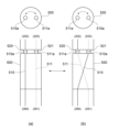
- FIG. 6 is a diagram illustrating an example of the configuration of the switch 280.
- the switch 280 may mechanically switch between a first connection state and a second connection state.
- the switch 280 may include a rotatable member 500, and a first wiring 510 and a second wiring 511 attached to the rotatable member 500.
- the rotatable member 500 can rotate 180 degrees to exchange the position of the terminal 510a of the first wiring 510 with the position of the terminal 511a of the second wiring 511.
- the rotatable member 500 can be switched between a first connection state (state (a) in Figure 6) and a second connection state (state (b) in Figure 6) by rotation.
- the first connection state (a) is a state in which the terminal 510a of the first wiring 510 is connected to the wiring terminal 520 connected to the substrate bias electrode 202, the first voltage pulse generator 260 is electrically connected to the substrate bias electrode 202, and further the terminal 511a of the second wiring 511 is connected to the wiring terminal 521 connected to the ring bias electrode 203, and the second voltage pulse generator 261 is electrically connected to the ring bias electrode 203.
- the second connection state (b) is a state in which the terminal 510a of the first wiring 510 is connected to the wiring terminal 521 of the ring bias electrode 203, the first voltage pulse generator 260 is electrically connected to the ring bias electrode 203, and further, the terminal 511a of the second wiring 511 is connected to the wiring terminal 520 of the substrate bias electrode 202, and the second voltage pulse generator 261 is electrically connected to the substrate bias electrode 202.
- a first voltage pulse having a first voltage level V1 generated by the first voltage pulse generator 260 is applied to the substrate bias electrode 202 shown in FIG. 3, and a second voltage pulse having a second voltage level V3 generated by the second voltage pulse generator 261 is applied to the ring bias electrode 203.
- a second voltage pulse having a second voltage level V3 generated by the second voltage pulse generator 261 is applied to the substrate bias electrode 202, and a first voltage pulse having a first voltage level V1 generated by the first voltage pulse generator 260 is applied to the ring bias electrode 203.
- the plasma processing method includes an etching process that uses plasma to etch a film on a substrate W.
- the plasma processing method is performed by a controller 2 in a plasma processing apparatus 1.
- the substrate W is carried into the chamber 10 by the transport arm, placed on the substrate support 11 by the lifter, and held by suction on the substrate support 11 as shown in FIG. 2.
- the processing gas is supplied to the shower head 13 by the gas supply unit 20, and is supplied from the shower head 13 to the plasma processing space 10s.
- the processing gas supplied at this time includes a gas that generates active species necessary for the etching process of the substrate W.
- One or more RF signals are supplied from the RF power supply 31 to the upper electrode and/or the lower electrode.
- the atmosphere in the plasma processing space 10s is exhausted from the gas exhaust port 10e, and the inside of the plasma processing space 10s may be depressurized. As a result, plasma is generated on the substrate support 11 in the plasma processing space 10s, and the substrate W is etched.
- a voltage pulse signal is supplied from the first voltage pulse generator 260 and the second voltage pulse generator 261 shown in FIG. 3 to the substrate bias electrode 202 and the ring bias electrode 203, and a voltage pulse is applied to each of them.
- a bias signal based on the voltage pulse is generated for the substrate W and the ring assembly 112, and the ion components in the plasma above the substrate W are attracted to the substrate W side.
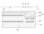
- the voltage level of the voltage pulse applied to the ring bias electrode 203 is made higher than the voltage level of the voltage pulse applied to the substrate bias electrode 202. That is, the switch 280 is switched to the first connection state (a), and a first voltage pulse signal DC3 having a first voltage level V1 is supplied from the first voltage pulse generator 260 to the substrate bias electrode 202, and a second voltage pulse signal DC4 having a second voltage level V3 higher than the first voltage level V1 is supplied from the second voltage pulse generator 261 to the ring bias electrode 203.
- the plasma sheath PS approaches parallel (horizontal) to the substrate W, and the angle at which the ion component of the plasma enters the substrate W (ion incidence angle) in the plane of the substrate W approaches perpendicular to the substrate W.
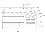
- the voltage level of the voltage pulse applied to the substrate bias electrode 202 is made higher than the voltage level of the voltage pulse applied to the ring bias electrode 203. That is, the switch 280 is switched to the second connection state (b), and a first voltage pulse signal DC3 having a first voltage level V1 is supplied from the first voltage pulse generator 260 to the ring bias electrode 203, and a second voltage pulse signal DC4 having a second voltage level V3 higher than the first voltage level V1 is supplied from the second voltage pulse generator 261 to the substrate bias electrode 202.
- the plasma sheath PS approaches parallel (horizontal) to the substrate W, and the angle at which the ion component of the plasma enters the substrate W (ion incidence angle) in the plane of the substrate W approaches perpendicular to the substrate W.
- the plasma processing apparatus 1 includes a substrate support 11, a substrate bias electrode 202, a ring bias electrode 203, a first voltage pulse generator 260, a second voltage pulse generator 261, and a switch 280.
- This makes it possible to control the ion incidence angle within the surface of the substrate W during plasma processing. As a result, it is possible to improve the uniformity within the surface of the substrate during plasma processing.
- the thickness of the ring assembly 112 at the time of shipment can be increased.
- the position of the upper surface 112a of the ring assembly 112 becomes higher, and the plasma sheath PS becomes higher above the ring assembly 112. Therefore, the switch 280 is switched to the second connection state (b), and the voltage level of the voltage pulse applied to the substrate bias electrode 202 is made higher than the voltage level of the voltage pulse applied to the ring bias electrode 203.
- the plasma sheath PS becomes closer to being parallel (horizontal) to the substrate W, and the angle at which the ion component of the plasma enters the substrate W (ion incidence angle) within the plane of the substrate W becomes closer to being perpendicular to the substrate W.
- the switch 280 is switched to the first connection state (a), and the voltage level of the voltage pulse applied to the ring bias electrode 203 is made higher than the voltage level of the voltage pulse applied to the substrate bias electrode 202.
- the plasma sheath PS becomes closer to parallel (horizontal) to the substrate W, and the angle at which the ion component of the plasma enters the substrate W (ion incidence angle) within the surface of the substrate W becomes closer to perpendicular to the substrate W.
- the usage period (life) of the ring assembly 112 can be extended and the number of times the ring assembly 112 needs to be replaced can be reduced.
- the substrate bias electrode 202 and the ring bias electrode 203 of the substrate support portion 11 may be disposed at different heights.
- the ring bias electrode 203 may be disposed at a lower position than the substrate bias electrode 202.
- the outer edge region 202a of the substrate bias electrode 202 may vertically overlap with the inner edge region 203a of the ring bias electrode 203.
- the radial width D1 of the overlapping portion of the substrate bias electrode 202 and the ring bias electrode 203 may be 9 mm to 11 mm.
- the ring bias electrode 203 may be positioned higher than the substrate bias electrode 202.
- the switch 280 mechanically switches between the first and second connection states, but it may be an electrical circuit that electrically switches between them.
- FIGS. 13 and 14 are diagrams for explaining a configuration example of the substrate support 11 and the DC power supply 32 in the second exemplary embodiment.
- the substrate support 11 may be the same as that in the first exemplary embodiment.
- the DC power supply 32 includes a first DC power supply 600, a second DC power supply 601, a voltage adder 610, a first voltage pulse generator 620, a second voltage pulse generator 621, and an impedance matcher 630.
- the first DC power source 600 may generate a first primary DC signal DC1 having a first primary voltage level V1.
- the first primary voltage level V1 may have a negative polarity.
- the first DC power source 600 is electrically connected to a voltage adder 610.
- the generated first primary DC signal DC1 may be supplied to the voltage adder 610.
- the second DC power source 601 may generate a second primary DC signal DC2 having a second primary voltage level V2.
- the second primary voltage level V2 may have a negative polarity.
- the second DC power source 601 is electrically connected to a voltage adder 610.
- the generated second primary DC signal DC2 may be supplied to the voltage adder 610.
- the absolute value of the first primary voltage level V1 may be greater than the absolute value of the second primary voltage level V2, and the absolute value of the first primary voltage level V1 may be five times or more greater than the absolute value of the second primary voltage level V2.
- the voltage adder 610 may use the first primary DC signal DC1 and the second primary DC signal DC2 to generate a first secondary DC signal DC3 having a first secondary voltage level and a second secondary DC signal DC4 having a second secondary voltage level.
- the voltage adder 610 is configured to switch between a first generation state and a second generation state.
- a first generation state as shown in FIG. 13
- a first secondary DC signal DC3 having a first secondary voltage level V1 that is the same voltage level as the first primary voltage level V1
- a second secondary DC signal DC4 having a second secondary voltage level V3 (V1+V2) that is the voltage level obtained by adding the first primary voltage level V1 and the second primary voltage level V2 is generated.
- V1+V2 second secondary DC signal DC4 having a second secondary voltage level V3
- a first secondary DC signal DC3 having a first secondary voltage level V3 (V1+V2) that is the voltage level obtained by adding the first primary voltage level V1 and the second primary voltage level V2 is generated, and a second secondary DC signal DC4 having a second secondary voltage level V1 that is the same voltage level as the first primary voltage level V1 is generated.
- the voltage adder 610 is electrically connected to the first voltage pulse generator 620 and the second voltage pulse generator 621.
- the first secondary DC signal DC3 generated by the voltage adder 610 can be supplied to the first voltage pulse generator 620, and the second secondary DC signal DC4 can be supplied to the second voltage pulse generator 621.
- the first voltage pulse generator 620 may generate a first voltage pulse signal DC5 having a first secondary voltage level (V1 or V3) from the first secondary DC signal DC3 supplied from the voltage adder 610.
- the first voltage pulse signal DC5 may include a sequence of first voltage pulses. In one embodiment, the sequence of first voltage pulses has a pulse pattern similar to the example shown in FIG. 5.
- the first voltage pulse generator 620 is electrically connected to the substrate bias electrode 202.
- the generated first voltage pulse signal DC5 may be supplied to the substrate bias electrode 202.
- a bias pulse signal based on a DC voltage is generated, and ion components in the plasma generated on the substrate W of the substrate support 11 can be attracted to the substrate bias electrode 202.
- the second voltage pulse generator 621 may generate a second voltage pulse signal DC6 having a second secondary voltage level (V1 or V3) from the second secondary DC signal DC4 supplied from the voltage adder 610.
- the second voltage pulse signal DC6 may include a sequence of second voltage pulses. In one embodiment, the sequence of second voltage pulses has a pulse pattern similar to the example shown in FIG. 5.
- the second voltage pulse generator 621 is electrically connected to the ring bias electrode 203.
- the generated second voltage pulse signal DC6 may be supplied to the ring bias electrode 203.
- a bias pulse signal based on a DC voltage is generated, and ion components in the plasma generated on the substrate W of the substrate support 11 can be attracted to the ring bias electrode 203.
- the voltage level of the voltage pulse applied to the ring bias electrode 203 is made higher than the voltage level of the voltage pulse applied to the substrate bias electrode 202. That is, as shown in FIG. 13, the voltage adder 610 is switched to the first generation state, and a first secondary DC signal DC3 having a first secondary voltage level V1 and a second secondary DC signal DC4 having a second secondary voltage level V3 are generated.
- a first voltage pulse signal DC5 having a first secondary voltage level V1 is supplied from the first voltage pulse generator 260 to the substrate bias electrode 202, and a voltage pulse signal DC6 having a second secondary voltage level V3 higher than the first secondary voltage level V1 is supplied from the second voltage pulse generator 261 to the ring bias electrode 203.
- the plasma sheath PS becomes closer to being parallel (horizontal) to the substrate W, and the angle at which the ion components of the plasma enter the substrate W within the plane of the substrate W (ion incidence angle) becomes closer to being perpendicular to the substrate W.
- the voltage level of the voltage pulse applied to the substrate bias electrode 202 is made higher than the voltage level of the voltage pulse applied to the ring bias electrode 203. That is, as shown in FIG. 14, the voltage adder 610 is switched to a second generation state, and a first secondary DC signal DC3 having a first secondary voltage level V3 and a second secondary DC signal DC4 having a second secondary voltage level V1 are generated.
- a first voltage pulse signal DC5 having a first secondary voltage level V3 higher than the second secondary voltage level V1 is supplied from the first voltage pulse generator 260 to the substrate bias electrode 202, and a voltage pulse signal DC6 having a second secondary voltage level V1 is supplied from the second voltage pulse generator 261 to the ring bias electrode 203.
- the plasma sheath PS becomes closer to being parallel (horizontal) to the substrate W, and the angle at which the ion components of the plasma enter the substrate W within the plane of the substrate W (ion incidence angle) becomes closer to being perpendicular to the substrate W.
- the substrate bias electrode 202 and the ring bias electrode 203 of the substrate support portion 11 may be disposed at different heights.
- the ring bias electrode 203 may be disposed at a lower position than the substrate bias electrode 202.
- the outer edge region 202a of the substrate bias electrode 202 may vertically overlap with the inner edge region 203a of the ring bias electrode 203.
- the ring bias electrode 203 may be disposed at a higher position than the substrate bias electrode 202.
- the ring chuck electrode 201 shown in FIG. 3 has two electrodes 400, 401 with different polarities, but it may have one electrode with a single polarity.
- the substrate bias electrode 202 and the ring bias electrode 203 may each be composed of multiple electrodes.
- a capacitively coupled plasma device has been described as an example, but the present invention is not limited to this and may be applied to other plasma devices.
- an inductively coupled plasma device may be used instead of a capacitively coupled plasma device.
- a plasma processing chamber a substrate support disposed within the plasma processing chamber, the substrate support including: a base; an electrostatic chuck disposed on the base, the electrostatic chuck having a substrate support surface and a ring support surface; and at least one annular member disposed on the ring support surface to surround a substrate disposed on the substrate support surface; a substrate chuck electrode disposed within the electrostatic chuck below the substrate support surface; at least one ring chuck electrode disposed within the electrostatic chuck below the ring support surface; a substrate bias electrode disposed within the electrostatic chuck and below the substrate chuck electrode; a ring bias electrode disposed within the electrostatic chuck and positioned below the at least one ring chuck electrode; a first voltage pulse generator configured to generate a sequence of first voltage pulses having a first voltage level; a second voltage pulse generator configured to generate a sequence of second voltage pulses having a second voltage level; a switch configured to switch between a first connection state and a second connection state, the first connection state being
- the switch is A rotatable member; a first wire and a second wire attached to the rotatable member; The first connection state and the second connection state are switched by rotating the rotatable member, the first connection state is a state in which the first voltage pulse generator is electrically connected to the substrate bias electrode via the first wiring, and the second voltage pulse generator is electrically connected to the ring bias electrode via the second wiring; the second connection state is a state in which the first voltage pulse generator is electrically connected to the ring bias electrode via the first wiring, and the second voltage pulse generator is electrically connected to the substrate bias electrode via the second wiring; 2.
- the switch is an electric circuit. 2.
- the ring bias electrode is disposed at a lower position than the substrate bias electrode.
- the substrate bias electrode has an outer edge region; 9.
- the ring bias electrode has an inner edge region that vertically overlaps the outer edge region of the substrate bias electrode.
- the ring chuck electrode is an inner ring chuck electrode to which a first ring chuck voltage having a first polarity is applied; an outer ring chuck electrode to which a second ring chuck voltage having a second polarity is applied; 10.
- the plasma processing apparatus according to claim 1 is an inner ring chuck electrode to which a first ring chuck voltage having a first polarity is applied; an outer ring chuck electrode to which a second ring chuck voltage having a second polarity is applied; 10.
- the plasma processing apparatus according to claim 1 .
- a plasma processing chamber a substrate support disposed within the plasma processing chamber, the substrate support including: a base; an electrostatic chuck disposed on the base, the electrostatic chuck having a substrate support surface and a ring support surface; and at least one annular member disposed on the ring support surface to surround a substrate disposed on the substrate support surface; a substrate chuck electrode disposed within the electrostatic chuck below the substrate support surface; at least one ring chuck electrode disposed within the electrostatic chuck below the ring support surface; a substrate bias electrode disposed within the electrostatic chuck and below the substrate chuck electrode; a ring bias electrode disposed within the electrostatic chuck and positioned below the at least one ring chuck electrode; a first DC power supply configured to generate a first primary DC signal having a first primary voltage level; a second DC power supply configured to generate a second primary DC signal having a second primary voltage level; a voltage adder configured to generate a first secondary DC signal having a first secondary voltage level and a second secondary
- an absolute value of the first primary voltage level is greater than or equal to five times the absolute value of the second primary voltage level; 14.
- the ring bias electrode is disposed at a lower position than the substrate bias electrode. 17.
- the substrate bias electrode has an outer edge region; 20.
- the ring chuck electrode is an inner ring chuck electrode to which a first ring chuck voltage having a first polarity is applied; an outer ring chuck electrode to which a second ring chuck voltage having a second polarity is applied; 19.
- the plasma processing apparatus according to any one of claims 11 to 18.
- REFERENCE SIGNS LIST 1 plasma processing apparatus, 10: chamber, 11: substrate support, 112: ring assembly, 1111: electrostatic chuck, 200: substrate chuck electrode, 201: ring chuck electrode, 202: substrate bias electrode, 203: ring bias electrode, 250: first DC power supply, 251: second DC power supply, 260: first voltage pulse generator, 261: second voltage pulse generator, 280: switch, W: substrate
Landscapes
- Physics & Mathematics (AREA)
- Engineering & Computer Science (AREA)
- Plasma & Fusion (AREA)
- Chemical & Material Sciences (AREA)
- Analytical Chemistry (AREA)
- Electromagnetism (AREA)
- Spectroscopy & Molecular Physics (AREA)
- Drying Of Semiconductors (AREA)
- Chemical Vapour Deposition (AREA)
Priority Applications (4)
| Application Number | Priority Date | Filing Date | Title |
|---|---|---|---|
| CN202480010890.6A CN120642034A (zh) | 2023-02-14 | 2024-01-19 | 等离子体处理装置 |
| JP2025500737A JPWO2024171714A1 (https=) | 2023-02-14 | 2024-01-19 | |
| KR1020257029719A KR20250150573A (ko) | 2023-02-14 | 2024-01-19 | 플라즈마 처리 장치 |
| US19/293,201 US20250364212A1 (en) | 2023-02-14 | 2025-08-07 | Plasma processing apparatus |
Applications Claiming Priority (2)
| Application Number | Priority Date | Filing Date | Title |
|---|---|---|---|
| JP2023-020626 | 2023-02-14 | ||
| JP2023020626 | 2023-02-14 |
Related Child Applications (1)
| Application Number | Title | Priority Date | Filing Date |
|---|---|---|---|
| US19/293,201 Continuation US20250364212A1 (en) | 2023-02-14 | 2025-08-07 | Plasma processing apparatus |
Publications (1)
| Publication Number | Publication Date |
|---|---|
| WO2024171714A1 true WO2024171714A1 (ja) | 2024-08-22 |
Family
ID=92421424
Family Applications (1)
| Application Number | Title | Priority Date | Filing Date |
|---|---|---|---|
| PCT/JP2024/001413 Ceased WO2024171714A1 (ja) | 2023-02-14 | 2024-01-19 | プラズマ処理装置 |
Country Status (6)
| Country | Link |
|---|---|
| US (1) | US20250364212A1 (https=) |
| JP (1) | JPWO2024171714A1 (https=) |
| KR (1) | KR20250150573A (https=) |
| CN (1) | CN120642034A (https=) |
| TW (1) | TW202503829A (https=) |
| WO (1) | WO2024171714A1 (https=) |
Families Citing this family (1)
| Publication number | Priority date | Publication date | Assignee | Title |
|---|---|---|---|---|
| WO2024024594A1 (ja) * | 2022-07-28 | 2024-02-01 | 東京エレクトロン株式会社 | プラズマ処理装置及び電源システム |
Citations (6)
| Publication number | Priority date | Publication date | Assignee | Title |
|---|---|---|---|---|
| JP2021158134A (ja) * | 2020-03-25 | 2021-10-07 | 東京エレクトロン株式会社 | 基板支持器及びプラズマ処理装置 |
| JP2022523069A (ja) * | 2019-02-01 | 2022-04-21 | アプライド マテリアルズ インコーポレイテッド | エッジリングの温度及びバイアスの制御 |
| WO2022168642A1 (ja) * | 2021-02-04 | 2022-08-11 | 東京エレクトロン株式会社 | プラズマ処理装置及びプラズマ処理方法 |
| JP2022184788A (ja) * | 2021-05-31 | 2022-12-13 | 東京エレクトロン株式会社 | プラズマ処理装置 |
| WO2022259793A1 (ja) * | 2021-06-08 | 2022-12-15 | 東京エレクトロン株式会社 | プラズマ処理装置 |
| JP2023010808A (ja) * | 2017-09-29 | 2023-01-20 | 住友大阪セメント株式会社 | 静電チャック装置 |
Family Cites Families (1)
| Publication number | Priority date | Publication date | Assignee | Title |
|---|---|---|---|---|
| US11848176B2 (en) | 2020-07-31 | 2023-12-19 | Applied Materials, Inc. | Plasma processing using pulsed-voltage and radio-frequency power |
-
2024
- 2024-01-19 JP JP2025500737A patent/JPWO2024171714A1/ja active Pending
- 2024-01-19 WO PCT/JP2024/001413 patent/WO2024171714A1/ja not_active Ceased
- 2024-01-19 CN CN202480010890.6A patent/CN120642034A/zh active Pending
- 2024-01-19 KR KR1020257029719A patent/KR20250150573A/ko active Pending
- 2024-01-31 TW TW113103684A patent/TW202503829A/zh unknown
-
2025
- 2025-08-07 US US19/293,201 patent/US20250364212A1/en active Pending
Patent Citations (6)
| Publication number | Priority date | Publication date | Assignee | Title |
|---|---|---|---|---|
| JP2023010808A (ja) * | 2017-09-29 | 2023-01-20 | 住友大阪セメント株式会社 | 静電チャック装置 |
| JP2022523069A (ja) * | 2019-02-01 | 2022-04-21 | アプライド マテリアルズ インコーポレイテッド | エッジリングの温度及びバイアスの制御 |
| JP2021158134A (ja) * | 2020-03-25 | 2021-10-07 | 東京エレクトロン株式会社 | 基板支持器及びプラズマ処理装置 |
| WO2022168642A1 (ja) * | 2021-02-04 | 2022-08-11 | 東京エレクトロン株式会社 | プラズマ処理装置及びプラズマ処理方法 |
| JP2022184788A (ja) * | 2021-05-31 | 2022-12-13 | 東京エレクトロン株式会社 | プラズマ処理装置 |
| WO2022259793A1 (ja) * | 2021-06-08 | 2022-12-15 | 東京エレクトロン株式会社 | プラズマ処理装置 |
Also Published As
| Publication number | Publication date |
|---|---|
| TW202503829A (zh) | 2025-01-16 |
| CN120642034A (zh) | 2025-09-12 |
| JPWO2024171714A1 (https=) | 2024-08-22 |
| KR20250150573A (ko) | 2025-10-20 |
| US20250364212A1 (en) | 2025-11-27 |
Similar Documents
| Publication | Publication Date | Title |
|---|---|---|
| JP2024168188A (ja) | 基板処理装置 | |
| US20250364212A1 (en) | Plasma processing apparatus | |
| JP2026012789A (ja) | プラズマ処理装置 | |
| JP2025179121A (ja) | プラズマ処理方法及びプラズマ処理装置 | |
| JP2025004870A (ja) | 基板支持器及びプラズマ処理装置 | |
| JP2024094874A (ja) | プラズマ処理装置 | |
| WO2024257401A1 (ja) | プラズマ処理装置 | |
| JP7583229B1 (ja) | 静電チャック | |
| WO2024252740A1 (ja) | プラズマ処理装置 | |
| WO2025169734A1 (ja) | プラズマ処理装置 | |
| WO2026004597A1 (ja) | プラズマ処理装置 | |
| US20250232954A1 (en) | Plasma processing apparatus and power supply system | |
| JP7723172B1 (ja) | 静電チャック | |
| WO2024070578A1 (ja) | プラズマ処理装置及び電源システム | |
| JP2024111591A (ja) | プラズマ処理装置 | |
| WO2026042553A1 (ja) | プラズマ処理装置及び電源システム | |
| JP2025127899A (ja) | プラズマ処理装置 | |
| JP2025173686A (ja) | プラズマ処理装置 | |
| JP2025029851A (ja) | プラズマ処理装置 | |
| WO2024204321A1 (ja) | エッチング装置及びエッチング方法 | |
| JP2025064037A (ja) | 静電チャック、基板支持器、及びプラズマ処理装置 | |
| JP2025090149A (ja) | プラズマ処理方法及びプラズマ処理装置 | |
| WO2024018960A1 (ja) | プラズマ処理装置及びプラズマ処理方法 | |
| WO2025263340A1 (ja) | 基板支持器及び基板処理装置 | |
| WO2026034233A1 (ja) | プラズマ処理装置及び電源システム |
Legal Events
| Date | Code | Title | Description |
|---|---|---|---|
| 121 | Ep: the epo has been informed by wipo that ep was designated in this application |
Ref document number: 24756565 Country of ref document: EP Kind code of ref document: A1 |
|
| ENP | Entry into the national phase |
Ref document number: 2025500737 Country of ref document: JP Kind code of ref document: A |
|
| WWE | Wipo information: entry into national phase |
Ref document number: 2025500737 Country of ref document: JP |
|
| WWE | Wipo information: entry into national phase |
Ref document number: 202480010890.6 Country of ref document: CN |
|
| ENP | Entry into the national phase |
Ref document number: 1020257029719 Country of ref document: KR Free format text: ST27 STATUS EVENT CODE: A-0-1-A10-A15-NAP-PA0105 (AS PROVIDED BY THE NATIONAL OFFICE) |
|
| WWP | Wipo information: published in national office |
Ref document number: 202480010890.6 Country of ref document: CN |
|
| NENP | Non-entry into the national phase |
Ref country code: DE |
|
| WWP | Wipo information: published in national office |
Ref document number: 1020257029719 Country of ref document: KR |
|
| 122 | Ep: pct application non-entry in european phase |
Ref document number: 24756565 Country of ref document: EP Kind code of ref document: A1 |