WO2024162015A1 - 撮像装置、データ処理方法、及び、記録媒体 - Google Patents
撮像装置、データ処理方法、及び、記録媒体 Download PDFInfo
- Publication number
- WO2024162015A1 WO2024162015A1 PCT/JP2024/001199 JP2024001199W WO2024162015A1 WO 2024162015 A1 WO2024162015 A1 WO 2024162015A1 JP 2024001199 W JP2024001199 W JP 2024001199W WO 2024162015 A1 WO2024162015 A1 WO 2024162015A1
- Authority
- WO
- WIPO (PCT)
- Prior art keywords
- processing
- imaging
- inference
- imaging device
- circuit
- Prior art date
- Legal status (The legal status is an assumption and is not a legal conclusion. Google has not performed a legal analysis and makes no representation as to the accuracy of the status listed.)
- Ceased
Links
Images











Classifications
-
- G—PHYSICS
- G06—COMPUTING OR CALCULATING; COUNTING
- G06T—IMAGE DATA PROCESSING OR GENERATION, IN GENERAL
- G06T7/00—Image analysis
-
- G—PHYSICS
- G06—COMPUTING OR CALCULATING; COUNTING
- G06V—IMAGE OR VIDEO RECOGNITION OR UNDERSTANDING
- G06V10/00—Arrangements for image or video recognition or understanding
- G06V10/70—Arrangements for image or video recognition or understanding using pattern recognition or machine learning
- G06V10/82—Arrangements for image or video recognition or understanding using pattern recognition or machine learning using neural networks
-
- H—ELECTRICITY
- H04—ELECTRIC COMMUNICATION TECHNIQUE
- H04N—PICTORIAL COMMUNICATION, e.g. TELEVISION
- H04N23/00—Cameras or camera modules comprising electronic image sensors; Control thereof
- H04N23/60—Control of cameras or camera modules
-
- H—ELECTRICITY
- H04—ELECTRIC COMMUNICATION TECHNIQUE
- H04N—PICTORIAL COMMUNICATION, e.g. TELEVISION
- H04N25/00—Circuitry of solid-state image sensors [SSIS]; Control thereof
- H04N25/70—SSIS architectures; Circuits associated therewith
Definitions
- This technology relates to an imaging device, a data processing method, and a recording medium, and to an imaging device, a data processing method, and a recording medium that improve the information security of an imaging device that has a processing circuit that performs inference processing built in.
- Patent documents 1 to 4 disclose technology that uses inference processing to generate a complementary image from an image obtained from an imaging element, and performs image recognition processing, etc., all within a single chip.
- This technology was developed in light of these circumstances, and aims to improve the information security of imaging devices that incorporate a processing circuit that performs inference processing.
- the imaging device or recording medium of the first aspect of the present technology has an imaging unit that captures an image, and a processing unit mounted on an integrated chip together with the imaging unit, the processing unit performing inference processing using the captured image captured by the imaging unit as input, and the processing unit is an imaging device that performs learning processing of an inference model used in the inference processing, or a recording medium on which a program is recorded to cause a computer to function as such a processing unit.
- the data processing method of the present technology is a data processing device having an imaging unit and a processing unit mounted together with the imaging unit on an integrated chip, the imaging unit captures an image, the processing unit performs inference processing using the captured image captured by the imaging unit as an input, and performs learning processing of an inference model used in the inference processing.
- an image is captured, an inference process is performed using the captured image as an input, and a learning process is performed on an inference model used in the inference process.
- the imaging device has an imaging unit that captures an image and a processing unit that performs inference processing, and the processing unit is an imaging device that performs the inference processing using an element characteristic value that indicates the characteristics of an element as an input.
- an image is captured, and inference processing is performed using element characteristic values indicating the characteristics of the element as input.
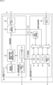
- FIG. 1 is a block diagram showing an example of the configuration of an embodiment of a digital camera to which the present technology is applied.
- FIG. 2 is a block diagram showing an example of a basic configuration of the imaging apparatus shown in FIG. 1 .
- FIG. 2 is a perspective view showing an outline of an external configuration example of the imaging device shown in FIG. 1 .
- FIG. 2 is a perspective view showing an outline of an external configuration example of the imaging device shown in FIG. 1 .
- FIG. 2 is a perspective view showing an outline of an external configuration example of the imaging device shown in FIG. 1 .
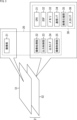
- FIG. 1 is an explanatory diagram of DNN processing in an imaging device.
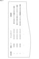
- FIG. 13 is a diagram showing an example of a log related to update processing of circuit setting values by DNN processing.
- FIG. 1 is a block diagram showing an example of the configuration of an embodiment of an imaging device to which the present technology is applied.
- FIG. 13 is a block diagram showing an example of the configuration of an imaging device according to another embodiment.
- FIG. 1 is a diagram illustrating an example of a circuit configuration of an imaging device as a stacked sensor.
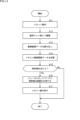
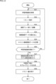
- 11 is a flowchart showing an example of the procedure of an inference process of an inference model that performs object detection using a captured image as input.
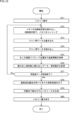
- 11 is a flowchart showing an example of the procedure of an inference process of an inference model that inputs internal element characteristics and outputs circuit setting values. This is a diagram explaining input/output data during learning of an inference model that uses internal element characteristics as input and feeds back circuit setting values.
- 11 is a flowchart showing an example of a procedure for determining a learning timing from an inference result in an inference process for detecting an object included in a captured image.
- 13 is a diagram showing an example of a processing procedure for detecting a change in the installation environment (deployment environment) and determining the timing for learning.
- 1 is a block diagram showing an example of the configuration of an embodiment of a computer to which the present technology is applied.
- This technology uses machine learning techniques to create an image sensor (imaging device) that detects device anomalies from the element characteristic values and environmental information (voltage, current, temperature, etc.) acquired on the sensor device, and feeds back circuit setting values to achieve optimal control in the target device.
- imaging device imaging device
- environmental information voltage, current, temperature, etc.
- An imaging device to which this technology is applied has a pixel section, a sensor control circuit, an AI processing circuit, and a memory device.
- the imaging device is equipped with a monitor circuit for acquiring element characteristic values for the pixel section, the sensor control circuit, and the memory device, and the output value of the monitor circuit is supplied to the AI processing circuit.
- the AI processing circuit uses inference processing to detect device abnormalities and optimal circuit setting values from the output value of the monitor circuit, etc.
- the pixel section, sensor control circuit, AI processing circuit, and memory device of the imaging device can be provided on a stacked chip.
- the communication paths within the imaging device are shielded from the outside, ensuring security and reducing the security risks of images being eavesdropped on or tampered with by malicious attackers, thereby improving information security.
- the AI processing circuit can perform the following six processes. Note that the learning process here refers to the "coefficient update process of the inference model.” (1) Inference processing for captured images (2) Learning processing using captured images (3) Inference processing for internal element characteristics (4) Learning processing using internal element characteristics (5) Inference processing for both captured images and internal element characteristics (6) Learning processing using both captured images and internal element characteristics
- FIG. 1 is a block diagram showing an example of the configuration of an embodiment of a digital camera to which the present technology is applied.
- the digital camera can capture both still images and videos.
- the digital camera has an optical system 1, an image capture device 2, a memory 3, a signal processing unit 4, an output unit 5, and a control unit 6.
- the optical system 1 includes, for example, a zoom lens, a focus lens, an aperture, etc. (not shown), and allows external light to enter the imaging device 2.
- the imaging device 2 is, for example, a CMOS (Complementary Metal Oxide Semiconductor) image sensor composed of one chip, which receives incident light from the optical system 1, performs photoelectric conversion, and outputs image data corresponding to the incident light from the optical system 1.
- CMOS Complementary Metal Oxide Semiconductor
- the memory 3 temporarily stores image data etc. output by the imaging device 2.
- the signal processing unit 4 performs camera signal processing using the image data stored in the memory 3, such as noise removal and white balance adjustment as necessary, and supplies the processed data to the output unit 5. Note that some or all of the processing performed by the memory 3 and the signal processing unit 4 may be performed by the memory and the signal processing unit of the imaging device 2.
- the output unit 5 outputs the image data from the signal processing unit 4 and the signal processing results stored in the memory 3. That is, the output unit 5 has a display (not shown) made of, for example, a liquid crystal or the like, and displays an image corresponding to the image data from the signal processing unit 4 as a so-called through image.
- the output unit 5 also has a driver (not shown) that drives a recording medium such as a semiconductor memory, a magnetic disk, or an optical disk, and records the image data from the signal processing unit 4 and the signal processing results stored in the memory 3 on the recording medium.
- a driver (not shown) that drives a recording medium such as a semiconductor memory, a magnetic disk, or an optical disk, and records the image data from the signal processing unit 4 and the signal processing results stored in the memory 3 on the recording medium.
- the output unit 5 functions, for example, as an I/F (Interface) that transmits data between an external device and the output unit 5, and transmits image data from the signal processing unit 4 and image data recorded on a recording medium to the external device.
- I/F Interface
- the control unit 6 controls each block that makes up the digital camera in accordance with user operations, etc.
- the imaging device 2 captures an image. That is, the imaging device 2 receives incident light from the optical system 1, performs photoelectric conversion, and obtains and outputs image data corresponding to the incident light.
- the image data output by the imaging device 2 is supplied to and stored in the memory 3.
- the image data stored in the memory 3 is subjected to camera signal processing by the signal processing unit 4, and the resulting image data is supplied to and output by the output unit 5.
- the imaging device 2 also performs signal processing using the image (data) obtained by imaging, and outputs the signal processing results.
- the signal processing results output by the imaging device 2 are stored in the memory 3, for example.
- the imaging device 2 selectively outputs the image itself obtained by imaging, and the results of signal processing using that image, etc.
- Fig. 2 is a block diagram showing an example of a basic configuration of the imaging device 2 in Fig. 1.
- the imaging device 2 has an imaging block 20 and a signal processing block 30.
- the imaging block 20 and the signal processing block 30 are electrically connected by connection lines (internal buses) CL1, CL2, and CL3.
- the imaging block 20 has an imaging section 21, an imaging processing section 22, an output control section 23, an output I/F (Interface) 24, and an imaging control section 25, and captures an image.
- the imaging unit 21 is composed of multiple pixels arranged two-dimensionally.
- the imaging unit 21 is driven by the imaging processing unit 22 to capture an image. That is, light from the optical system 1 ( Figure 1) is incident on the imaging unit 21.
- the imaging unit 21 receives the incident light from the optical system 1 at each pixel, performs photoelectric conversion, and outputs an analog image signal corresponding to the incident light.
- the size of the image (signal) output by the imaging unit 21 can be selected from multiple sizes, such as 12M (3968 x 2976) pixels and VGA (Video Graphics Array) size (640 x 480 pixels).
- the imaging unit 21 it is possible to select, for example, whether to output an RGB (red, green, blue) color image or a black and white image with luminance only. These selections can be made as a type of shooting mode setting.
- RGB red, green, blue
- the imaging processing unit 22 performs imaging processing related to the capture of an image by the imaging unit 21, such as driving the imaging unit 21, AD (Analog to Digital) conversion of the analog image signal output by the imaging unit 21, and imaging signal processing, under the control of the imaging control unit 25.
- AD Analog to Digital
- imaging signal processing includes, for example, a process for calculating the brightness of each small area of the image output by the imaging unit 21 by calculating the average pixel value for each predetermined small area, a process for converting the image output by the imaging unit 21 into an HDR (High Dynamic Range) image, defect correction, development, etc.
- HDR High Dynamic Range
- the imaging processing unit 22 outputs, as a captured image, a digital image signal (here, for example, an image of 12 megapixels or VGA size) obtained by AD conversion or the like of the analog image signal output by the imaging unit 21.
- the captured image output by the imaging processing unit 22 is supplied to the output control unit 23 and also to the image compression unit 35 of the signal processing block 30 via the connection line CL2.
- the output control unit 23 is also supplied with the results of signal processing using the captured images, etc. from the signal processing block 30 via the connection line CL3.
- the output control unit 23 performs output control to selectively output the captured image from the imaging processing unit 22 and the signal processing results from the signal processing block 30 from the (single) output I/F 24 to the outside (for example, memory 3 in FIG. 1). That is, the output control unit 23 selects the captured image from the imaging processing unit 22 or the signal processing results from the signal processing block 30 and supplies them to the output I/F 24.
- the output I/F 24 is an I/F that outputs the captured image and the signal processing results supplied from the output control unit 23 to the outside.
- a relatively high-speed parallel I/F such as MIPI (registered trademark) (Mobile Industry Processor Interface) can be adopted.
- MIPI registered trademark
- the captured image from the imaging processing unit 22 or the signal processing results from the signal processing block 30 are output to the outside according to the output control of the output control unit 23. Therefore, for example, when only the signal processing results from the signal processing block 30 are required outside and the captured image itself is not required, it is possible to output only the signal processing results, and the amount of data output from the output I/F 24 to the outside can be reduced.
- the signal processing block 30 performs signal processing to obtain the signal processing results required externally, and the signal processing results are output from the output I/F 24, eliminating the need to perform signal processing externally and reducing the load on external blocks.
- the imaging control unit 25 has a communication I/F 26 and a register group 27.
- the communication I/F 26 is a first communication I/F, such as a serial communication I/F such as I2C (Inter-Integrated Circuit), and exchanges necessary information, such as information to be read and written to the register group 27, with the outside (such as the control unit 6 in FIG. 1).
- I2C Inter-Integrated Circuit
- the register group 27 has multiple registers and stores imaging information related to the imaging of an image by the imaging unit 21, as well as various other information.
- the register group 27 stores imaging information received from the outside via the communication I/F 26, and the results of imaging signal processing by the imaging processing unit 22 (e.g., the brightness of each small area of the captured image, etc.).
- the imaging information stored in the register group 27 includes, for example, ISO sensitivity (analog gain during AD conversion in the imaging processing unit 22), exposure time (shutter speed), frame rate, focus, shooting mode, cropping range, etc. (information representing the same).
- Shooting modes include, for example, a manual mode in which the exposure time, frame rate, etc. are set manually, and an automatic mode in which the settings are automatically set according to the scene.
- the automatic mode includes modes that correspond to various shooting scenes, such as night scenes and human faces.
- the cut-out range refers to the range cut out from the image output by the imaging unit 21 when the imaging processing unit 22 cuts out a part of the image output by the imaging unit 21 and outputs it as a captured image.
- the cut-out range it is possible to cut out, for example, only the range in which a person appears from the image output by the imaging unit 21. Note that, in addition to a method of cutting out an image from the image output by the imaging unit 21, there is also a method of reading out only the image (signal) of the cut-out range from the imaging unit 21.
- the imaging control unit 25 controls the imaging processing unit 22 according to the imaging information stored in the register group 27, thereby controlling the imaging of an image by the imaging unit 21.
- the register group 27 can store the imaging information, the results of imaging signal processing by the imaging processing unit 22, as well as output control information related to output control by the output control unit 23.
- the output control unit 23 can perform output control to selectively output the captured image and the signal processing results according to the output control information stored in the register group 27.
- the imaging control unit 25 and the CPU 31 of the signal processing block 30 are connected via a connection line CL1, and the CPU 31 can read and write information from the register group 27 via the connection line CL1. That is, in the imaging device 2, reading and writing information from the register group 27 can be performed not only from the communication I/F 26 but also from the CPU 31.
- the signal processing block 30 has a CPU (Central Processing Unit) 31, a DSP (Digital Signal Processor) 32, a memory 33, a communication I/F 34, an image compression unit 35, and an input I/F 36, and performs predetermined signal processing using the captured image obtained by the imaging block 10.
- the CPU 31 and the input I/F 36 that make up the signal processing block 30 are connected to each other via a bus, and can exchange information as necessary.
- the CPU 31 executes the programs stored in the memory 33 to control the signal processing block 30, read and write information to and from the register group 27 of the imaging control unit 25 via the connection line CL1, and perform various other processes.
- the CPU 31 functions as an imaging information calculation unit that calculates imaging information using the signal processing results obtained by signal processing in the DSP 32, and feeds back and stores new imaging information calculated using the signal processing results to the register group 27 of the imaging control unit 25 via the connection line CL1. Therefore, the CPU 31 can ultimately control imaging in the imaging unit 21 and imaging signal processing in the imaging processing unit 22 according to the signal processing results of the captured image.
- the imaging information stored in the register group 27 by the CPU 31 can be provided (output) to the outside from the communication I/F 26.
- focus information from the imaging information stored in the register group 27 can be provided from the communication I/F 26 to a focus driver (not shown) that controls the focus.
- the DSP 32 executes a program stored in the memory 33 to function as a signal processing unit that performs signal processing using the captured image supplied to the signal processing block 30 from the imaging processing unit 22 via the connection line CL2 and information received from the outside by the input I/F 36.
- the memory 33 is composed of a static random access memory (SRAM) or a dynamic RAM (DRAM), and stores data necessary for the processing of the signal processing block 30.
- the memory 33 stores programs received from outside via the communication I/F 34, captured images compressed by the image compression unit 35 and used in signal processing in the DSP 32, the signal processing results of the signal processing performed by the DSP 32, information received by the input I/F 36, etc.
- the communication I/F 34 is a second communication I/F, for example a serial communication I/F such as SPI (Serial Peripheral Interface), and exchanges necessary information such as programs executed by the CPU 31 and DSP 32 with the outside (for example, the memory 3 and control unit 6 in FIG. 1).
- the communication I/F 34 downloads programs to be executed by the CPU 31 and DSP 32 from the outside, and supplies them to the memory 33 for storage. Therefore, depending on the programs downloaded by the communication I/F 34, various processes can be executed by the CPU 31 and DSP 32.
- the communication I/F 34 can exchange any data, in addition to programs, with the outside.
- the communication I/F 34 can output to the outside the signal processing results obtained by the signal processing in the DSP 32.
- the communication I/F 34 can also output information according to the instructions of the CPU 31 to an external device, thereby controlling the external device according to the instructions of the CPU 31.
- the signal processing results obtained by the signal processing in the DSP 32 can be output to the outside from the communication I/F 34, and can also be written by the CPU 31 to the register group 27 of the imaging control unit 25.
- the signal processing results written to the register group 27 can be output to the outside from the communication I/F 26. The same applies to the processing results performed by the CPU 31.
- the captured image is supplied to the image compression unit 35 from the imaging processing unit 22 via the connection line CL2.
- the image compression unit 35 performs a compression process to compress the captured image, and generates a compressed image with a smaller amount of data than the captured image.
- the compressed image generated by the image compression unit 35 is supplied to the memory 33 via the bus and stored there.
- the signal processing in the DSP 32 can be performed using the captured image itself, or using a compressed image generated from the captured image by the image compression unit 35. Since the compressed image has a smaller amount of data than the captured image, it is possible to reduce the load of signal processing in the DSP 32 and save the storage capacity of the memory 33 that stores the compressed image.
- the compression process in the image compression unit 35 can be, for example, scaling down a captured image of 12M (3968 x 2976) pixels to a VGA size image. If the signal processing in the DSP 32 is performed on luminance and the captured image is an RGB image, the compression process can be YUV conversion to convert the RGB image to a YUV image, for example.
- the image compression unit 35 can be realized by software or by dedicated hardware.
- the captured image supplied from the imaging processing unit 22 through the connection line CL2 can be stored in the memory 33 as is without being compressed by the image compression unit 35.
- the captured image has been compressed by the image compression unit 35, it will be referred to simply as the captured image without being distinguished from an uncompressed captured image.
- the input I/F 36 is an I/F that receives information from the outside.
- the input I/F 36 receives the output of an external sensor (external sensor output) from the external sensor, and supplies it to the memory 33 via the bus for storage.
- an external sensor external sensor output
- a parallel I/F such as MIPI (registered trademark) (Mobile Industry Processor Interface) can be used, as in the output I/F 24.
- MIPI registered trademark
- the external sensor for example, a distance sensor that senses information related to distance can be used.
- an image sensor that senses light and outputs an image corresponding to that light that is, an image sensor separate from the imaging device 2 can be used.
- the DSP 32 can also perform signal processing using the external sensor output received by the input I/F 36 from the external sensor described above and stored in the memory 33.
- the one-chip imaging device 2 configured as described above, signal processing is performed in the DSP 32 using the captured image (compressed image generated from the captured image) obtained by imaging in the imaging section 21, and the signal processing result of the signal processing and the captured image are selectively output from the output I/F 24. Therefore, it is possible to configure a compact imaging device that outputs information required by the user.
- the DSP 32 performs AI (Artificial Intelligence) processing based on the captured image and the element characteristic values described below.
- AI processing is processing that artificially realizes intelligence similar to that of humans on a computer, and includes, for example, inference processing (inference processing using an algorithm of the DNN) using an inference model (machine learning model) having a neural network (NN) structure in machine learning technology, particularly a deep neural network (DNN).
- inference processing using the DNN inference model is performed as the AI processing.
- the configuration of the signal processing block 30 is not limited to the case of FIG. 2, and is not limited to the case where the AI processing is performed by the DSP 32.
- the component that performs the AI processing is not limited to the DSP 32, and the signal processing block 30 performs the AI processing.
- the signal processing block 30 performs a process of updating (learning) the parameters (weights, biases, etc.) of the inference model (referred to as an update process or learning process of the inference model).
- AI processing includes inference processing by AI (inference processing using a DNN inference model) and learning processing for inference processing (learning processing of parameters (weights, biases, etc.) of the DNN inference model).
- FIG. 3 is a perspective view showing an example of the external configuration of the imaging device 2 in FIG. 1.
- the imaging device 2 can be configured as a one-chip semiconductor device having a stacked structure in which multiple dies are stacked, as shown in FIG. 3, for example.
- the imaging device 2 is a stacked chip in which two dies (substrates), dies 51 and 52, are stacked and integrated into one chip.
- the upper die 51 is equipped with the imaging unit 21, and the lower die 52 is equipped with the imaging processing unit 22 through the imaging control unit 25, and the CPU 31 through the input I/F 36.
- the upper die 51 and the lower die 52 are electrically connected, for example, by forming a through hole that passes through the die 51 and reaches the die 52, or by performing Cu-Cu bonding that directly connects the Cu wiring exposed on the underside of the die 51 with the Cu wiring exposed on the upper side of the die 52.
- the imaging processing unit 22 can adopt, for example, a column-parallel AD method or an area AD method as a method for performing AD conversion of the image signal output by the imaging unit 21.
- a column-parallel AD method for example, an ADC (AD Converter) is provided for each column of pixels that make up the imaging unit 21, and the ADC for each column is responsible for AD conversion of the pixel signals of the pixels in that column, thereby performing AD conversion of the image signals of the pixels in each column of one row in parallel.
- the column-parallel AD method part of the imaging processing unit 22 that performs AD conversion using the column-parallel AD method may be mounted on the upper die 51.
- the pixels that make up the imaging unit 21 are divided into multiple blocks, and an ADC is provided for each block.
- the ADC of each block is then responsible for AD conversion of the pixel signals of the pixels in that block, so that AD conversion of the image signals of the pixels in multiple blocks is performed in parallel.
- the block is the smallest unit, and AD conversion (readout and AD conversion) of the image signal can be performed only on the necessary pixels among the pixels that make up the imaging unit 21.
- the imaging device 2 can be configured as a single die (chip).
- two dies 51 and 52 are stacked to form a one-chip imaging device 2, but the one-chip imaging device 2 can be formed by stacking three or more dies.
- the memory 33 in FIG. 3 can be mounted on a separate die.
- the imaging device 2 may be configured as shown in Figs. 4 and 5.
- Figs. 4 and 5 the parts common to Fig. 3 and the imaging device 2 and the parts common to Figs. 4 and 5 are given the same reference numerals, and the description will be omitted as appropriate.
- the imaging device 2 in Fig. 4 has two independent printed circuit boards 71A and 71B. Two dies 51 and 52A and an external I/F 53A are mounted on the printed circuit board 71A. The dies 51 and 52A are stacked to form a single chip.
- the dies 51 and 52A are electrically connected to each other by Cu-Cu bonding, in which the Cu wiring exposed on the lower surface side of the die 51 is directly connected to the Cu wiring exposed on the upper surface side of the die 52A, as in the case of the dies 51 and 52 in Fig. 3.
- the die 52A and the external I/F 53A are electrically connected to each other, for example, via wiring printed on the printed circuit board 71A.
- the die 51 is equipped with an imaging unit 21, similar to the die 51 in FIG. 3, and the die 52A is equipped with imaging processing and control units 22, 25, which are part of the components equipped on the die 52 in FIG. 3.
- the imaging control and processing units 22, 25 are components that include the imaging processing unit 22 and the imaging control unit 25.
- the imaging processing and control units 22, 25 supply the captured image output from the imaging processing unit 22 and information input/output to the imaging control unit 25 to the external I/F 53A, or obtain it from the external I/F 53A.
- the printed circuit board 71B is equipped with the die 52B and the external I/F 53B.
- the die 52B and the external I/F 53B are electrically connected, for example, via wiring printed on the printed circuit board 71B.
- the die 52B is equipped with components including the signal processing block 30, which is part of the components mounted on the die 52 in FIG. 5.
- the output control unit 23 and the output I/F 24 are mounted on the die 52B.
- the components mounted on the die 52 in FIG. 3 may be divided and mounted on the die 52A and the die 52B, and some of the components may be mounted in duplicate. Therefore, for example, the die 52B may be equipped with a processing unit that performs DNN processing (AI processing) among the processes of the signal processing block 30, and a processing unit that performs processes other than DNN processing may be mounted on the die 51A.
- DNN processing AI processing
- the external I/F 53A of the printed circuit board 71A and the external I/F 53B of the printed circuit board 71B are connected to be able to communicate with each other, for example, via a LAN (Local Area Network). Through communication between these external I/Fs 53A and 53B, various information such as captured images is exchanged between the imaging processing and control unit 25 of the die 52A and the signal processing block 30 of the die 52B.
- LAN Local Area Network
- the imaging device 2 in FIG. 5 has a single printed circuit board 72.
- Two dies 51 and 52A which are the same as the dies 51, 52A, and 52B in FIG. 4, and an external I/F 53A are mounted on the printed circuit board 72.
- the dies 51 and 52A are stacked to form a single chip.
- the dies 51 and 52A are electrically connected to each other by Cu-Cu bonding, in which the Cu wiring exposed on the lower surface of the die 51 is directly connected to the Cu wiring exposed on the upper surface of the die 52A, as in the case of the dies 51 and 52 in FIG. 3.
- the dies 51, 52A, and 52B are respectively equipped with the imaging unit 21, the imaging processing and control units 22 and 25, and the signal processing unit lock 30, as in the case of the dies 51, 52A, and 52B in FIG. 4.
- the dies 52A and 52B are electrically connected to each other, for example, via wiring printed on the printed circuit board 71A. This wiring connection allows the exchange of various information, such as captured images, between the imaging control and processing unit 25 of die 52A and the signal processing block 30 of die 52B.
- the imaging device 2 in Fig. 3 has the lowest security risk.
- the imaging device 2 in Fig. 4 there is a risk that data such as captured images transmitted between the printed circuit board 71A (external I/F 53A) and the printed circuit board 71B (external I/F 53B) may be probed.
- the imaging device 2 in Fig. 5 there is a risk that data such as captured images transmitted between the die 52A and the die 52B may be probed.
- such a risk is extremely low.
- the imaging device 2 in Fig. 3 is more advantageous in miniaturizing the imaging device 2 than the imaging devices 2 in Figs. 4 and 5, and is more advantageous in speeding up the transmission of captured image data from the imaging processing unit 22 to the output control unit 23.
- the signal processing performed by the imaging device 2 may employ, for example, DNN processing (AI processing), as well as fusion processing and self-location estimation processing (SLAM: Simultaneously Localization and Mapping).
- DNN processing AI processing
- SLAM Simultaneously Localization and Mapping
- the imaging device 2 receives the output of a distance sensor, such as a ToF (Time of Flight) sensor, arranged to have a predetermined positional relationship with the imaging device 2, via the input I/F 36.
- the DSP 32 integrates the output of the distance sensor and the captured image to determine a highly accurate distance, such as a process of removing noise in a distance image obtained from the output of the distance sensor using the captured image.
- the imaging device 2 receives, via the input I/F 36, an image output by an image sensor arranged to have a predetermined positional relationship with the imaging device 2.
- the DSP 32 performs self-location estimation using the image from the input I/F 36 and the captured image as a stereo image.
- DNN processing is performed as the signal processing of DSP32.
- the DNN processing in the imaging device 2 will be described with reference to Fig. 6.
- the DNN processing in the imaging device 2 is performed by the signal processing block 30 in Fig. 2, and the signal processing block 30 can receive the captured image from the imaging unit 21 and the internal element characteristics (element characteristic values indicating the internal element characteristics) of the imaging device 2 from a monitor circuit described later.
- the signal processing block 30 can perform the following DNN processing such as (1) to (4).
- DNN processing for captured images As the DNN processing in the imaging device 2, image recognition such as object detection and segmentation by DNN processing (inference processing) using machine learning techniques such as Convolutional Neural Network (CNN), Generative Adversarial Network (GAN), and Transformer technology, and generation of various processed images such as image compression and high resolution (super resolution) can be performed.
- the input to the inference model used in the DNN processing is the captured image acquired by the imaging unit 21 as shown in FIG. 6, and the output from the inference model may be an image processed by the DNN processing (corrected image), metadata (inference result), or both.
- the inference model used in the DNN processing is also simply referred to as the inference model.
- DNN processing in the imaging device 2 may include detection of abnormalities in various elements constituting the imaging device 2, estimation of appropriate circuit setting values (such as a core power supply voltage and a bias voltage/current supplied to each module of the imaging device 2) to be fed back to the internal circuit of the imaging device 2, etc.
- the input to the inference model is the characteristics (internal element characteristics) of the elements constituting the imaging device 2 as shown in FIG. 6.
- Values indicating the internal element characteristics (element characteristic values) may be obtained from a monitor circuit arranged inside the imaging device 2.
- the output from the inference model may be the circuit setting values, (the results of) abnormality detection, or both.
- the element characteristic values input to the inference model include the following examples:
- the element characteristic values input to the inference model may be one type or a combination of multiple types of element characteristic values.
- signal line voltage, power supply noise, and surrounding environment information when pixel signals are read out for each column from the pixel array unit
- signal line voltage, power supply noise, and surrounding environmental information temperature, gyro, etc.
- signal line voltage, power supply noise, and surrounding environmental information when reading each word - Supply voltage and current consumption waveforms for each block (especially the power supply waveforms and current consumption values when Dynamic Voltage and Frequency Scaling (DVFS) technology is applied as a low-power technology
- circuit setting values (control parameters) output from the inference model include the following:
- the circuit setting values output from the inference model may be one or any combination of multiple circuit setting values.
- DNN processing of captured image and internal element characteristics As the DNN processing in the imaging device 2, image recognition by DNN processing, generation of a corrected image, etc. can be performed as in (1).
- the input to the inference model is both the captured image and the internal element characteristics
- the output from the inference model is a corrected image, metadata (inference result), or both.
- a learning process (update process) of the inference model i.e., an update of the parameters (weight coefficient, bias, etc.) of the inference model
- the error backpropagation method may be adopted as the learning process of the inference model.
- the captured image and element characteristic values are stored as learning data in the internal memory of the imaging device 2, and the optimal parameters of the inference model are calculated by the error backpropagation method using the stored learning data.
- the parameters of the inference model after the learning process are updated to the calculated optimal parameters.
- the timing (learning timing) for performing the learning process of the inference model can be determined on-chip.
- the following method can be applied. Note that, when learning data (teacher data) such as captured images used in the learning process of the inference model is newly acquired, the learning process includes a process for acquiring (collecting) the learning data, and the learning timing is the timing for starting to acquire the learning data.
- the first determination method when an inference model outputs certainty for multiple classes as an inference result, if it is determined that the peak of the certainty distribution for each class output by the inference model has dropped (if it is determined that the distribution does not have a large peak and that the object (class) has not been estimated with a significant difference), for example, if the certainty distribution for each class does not show a peak larger than a predetermined determination value, or if the certainty of none of the classes shows a certainty larger than a predetermined difference with respect to the certainty of the other classes, it is determined (determined) that it is time to learn. Also, it may be determined that it is time to learn when the difference between the first and second largest certainty among the certainties for each class is equal to or smaller than a threshold value, or when the largest (maximum) certainty is smaller than a threshold value.
- the timing of learning is determined (determined) when the placement environment of the imaging device 2 is updated (changed). Whether or not the placement environment of the imaging device 2 has been updated can be determined based on, for example, information about the environment in which the imaging device 2 is placed (temperature, brightness, gravity, etc.). The information about the environment is detected by a sensor built into the imaging device 2 or a sensor separate from the imaging device 2, and is supplied to the imaging device 2.
- the third determination method when it is determined that the element characteristic value inside the imaging device 2 is an abnormal value, or when the change in the element characteristic value exceeds a predetermined threshold, it is determined (determined) that it is time to learn.
- the motion detection sensor receives an input from the image capture device 2 that deviates from the regular movement of an object, it is determined (determined) as the timing to learn.
- the learning timing may be determined based on an external signal supplied to the imaging device 2.
- the imaging device 2 may have a mechanism (function) for saving and outputting information on the circuit setting value update processing, i.e., information showing how the circuit setting value was inferred and determined, as a history (log).
- the log is saved in the memory 33 of the imaging device 2 when the circuit setting value update processing by the DNN processing is executed, and is output to the external device when requested by the external device.
- FIG. 7 is a diagram showing an example of a log on the circuit setting value update processing by the DNN processing. In FIG.
- the information of the log includes information such as an execution number, a processing code, a timestamp, input information (not shown), and a processing result.
- the execution number is a sequence indicating the order in which the circuit setting value update processing was executed.
- the processing code is a code assigned to each execution of the circuit setting value update processing.
- the timestamp is the time when the circuit setting value change processing was executed.
- the input information is the internal element characteristic (element characteristic value) input to the DNN processing (inference model) during the circuit setting value update processing.
- the processing results are the circuit setting values updated by the circuit setting value update process.
- FIG. 7 shows, as examples of updated circuit setting values, the bias voltage setting value of element xxx, the changeover switch setting value of element yyy, and the clock frequency setting value for element zzz.
- the learning process of the inference model in the imaging device 2 of the present technology in addition to the general learning method described above, the following learning method can be used.
- a process of changing the circuit setting value for a memory element (memory 33) is performed as the DNN process.
- the learning process of the inference model used to infer the circuit setting value for example, data is read and written to a test cell in memory 33, and the learning process of the inference model is performed in a state where it is possible to obtain output data that is the correct answer.
- detection of anomalies in internal elements of the imaging device 2 detection of abnormal operation
- the learning process of the inference model used to detect anomalies in the internal elements is performed using only data during normal operation defined by the user or system.
- the inference model evaluates how much the data input to the inference model differs from the data used during learning, and abnormal operation of the elements is detected based on the evaluation results (see non-patent literature: J. Yu, et al., "FastFlow: Unsupervised Anomaly Detection and Localization via 2D Normalizing Flows,” arXiv:2111.07677, etc.).
- the DNN processing is performed using an inference model that mainly uses captured images as input.
- the learning process of the inference model can use a label-free learning method (unsupervised learning) without specially preparing correct answer labels.
- label-free learning methods unsupervised learning
- Many techniques have been proposed for label-free learning methods, so a detailed explanation will be omitted (for example, non-patent literature: T. Chen, et al., "A Simple Framework for Contrastive Learning of Visual Representations" arXiv:2002.05709).
- Fig. 8 is a block diagram showing a configuration example of an embodiment of an imaging device 2 to which the present technology is applied.
- Fig. 8 shows components of the imaging device 2 that are not shown in Figs. 2 to 5, and also shows components that embody or abstract some of the components in Figs. 2 to 5.
- the imaging device 2 has a pixel array section 101, a vertical scanning circuit 102, an AD conversion circuit 103, a control circuit 104, a signal processing circuit 105, a memory 106, an input/output section 107, and an element characteristic monitor circuit 108.
- the pixel array section 101 is a component that has the function of the imaging section 21 in FIG. 2.
- the pixel array section 101 has, for example, a plurality of pixel circuits arranged in a matrix array in the horizontal direction (row direction) and the vertical direction (column direction). Each pixel circuit includes a photoelectric conversion element that performs photoelectric conversion on the received light, and a circuit that reads out the charge from the photoelectric conversion element.
- the row direction arrangement of the pixel circuits is called a line.
- a line For example, in a pixel array section 100 having X pixel circuits per line and Y lines, one frame of an image (image data) can be formed by (X ⁇ Y) pixels (pixel signals).
- the pixel array section 101 may also include a Dual PD (Photodiode), ToF, EVS (Event-based Vision Sensor), etc.
- the vertical scanning circuit 102 is part of the circuit that drives the imaging unit 21 in the imaging processing unit 22 in FIG. 2.
- the vertical scanning circuit 102 supplies control signals for reading out pixel signals to the pixel circuits of the pixel array unit 101 for each line under the control of the control circuit 104.
- the lines to which the control signals are supplied are switched in the vertical direction, and the pixel signals are read out from the pixel circuits for each line and transmitted to the AD conversion circuit 103.
- the AD conversion circuit 103 is a circuit section included in the image capture processing section 22 in FIG. 2.
- the AD conversion circuit 103 converts the pixel signal (analog image signal) from the pixel array section 101 into a digital image signal by AD conversion or the like, and supplies it to the signal processing circuit 105 as a captured image.
- the control circuit 104 includes a circuit section that executes the processing of the imaging control section 25 in FIG. 2, and controls the AD conversion circuit 103, the signal processing circuit 105, the memory 106, the input/output section 107, and the element characteristic monitor circuit 108.
- the control circuit 104 controls the vertical scanning circuit 1012, the AD conversion circuit 103, etc., to control the imaging of images in the pixel array section 101.
- the signal processing circuit 105 is a circuit section that executes the imaging processing in the imaging processing section 22 in FIG. 2 and the processing of the signal processing block 30.
- the signal processing circuit 105 includes a circuit section (DNN processing circuit 126 in FIG. 10) that executes the above-mentioned DNN processing (AI processing).
- the captured image and the signal processing results processed by the signal processing circuit 105 are supplied to the input/output section 107.
- the signal processing circuit 105 may have multiple circuit sections (e.g., multiple processors).
- the signal processing circuit 105 is configured with a DNN processing circuit 126 that executes processing including DNN processing, and a signal processing circuit 125 that executes processing other than the processing in the DNN processing circuit 126.
- Memory 106 corresponds to memory 33 of signal processing block 30 in FIG. 2.
- Memory 106 includes volatile memory for buffering images and intermediate data, and non-volatile memory for storing parameters (weights, etc.) of the inference model in DNN processing.
- the input/output unit 107 is a circuit unit that includes the output control unit 23 and the output I/F 24 of the imaging block 20 in FIG. 2, and the input I/F 36 of the signal processing block 30. Note that the communication I/Fs 26 and 34 in FIG. 2 may be included in the input/output unit 107.
- the element characteristic monitor circuit 108 (hereinafter referred to as the monitor circuit 108) is a circuit section that detects the internal element characteristics of the imaging device 2.
- the monitor circuit 108 detects element characteristic values that indicate the element characteristics of each module of the pixel array section 101 to the input/output section 107 of the imaging device 2, and stores them in the memory 106.
- the element characteristic values detected by the monitor circuit 108 may be supplied to the signal processing circuit 105 (DNN processing circuit 126) instead of being stored in the memory 106.
- the element characteristic values detected by the monitor circuit 108 are used as input to an inference model in the DNN processing of the internal element characteristics in the signal processing circuit 105 when detecting an abnormality in an element (module) that constitutes the imaging device 2, or estimating an appropriate circuit setting value to be fed back to the internal circuit of the imaging device 2.
- the element characteristic values stored in the memory 106 are also used in the learning process of the inference model. If an abnormality is detected in the element, an abnormality detection signal indicating this is output from the signal processing circuit 105 (DNN processing circuit 126 in FIG. 10) to an external system or the control circuit 104.
- FIG. 9 is a block diagram showing an example of the configuration of another embodiment of the imaging device 2.
- parts common to the imaging device 2 in Fig. 8 are given the same reference numerals, and descriptions thereof will be omitted as appropriate.
- the imaging device 2 in FIG. 9 has a pixel array section 101, a vertical scanning circuit 102, an AD conversion circuit 103, a control circuit 104, a signal processing circuit 105, a memory 106, an input/output section 107, and monitor circuits 108A to 108G. Therefore, the imaging device 2 in FIG. 9 has the pixel array section 101, the vertical scanning circuit 102, the AD conversion circuit 103, the control circuit 104, the signal processing circuit 105, a memory 106, and an input/output section 107 in common with the imaging device 2 in FIG. 8. However, the imaging device 2 in FIG. 9 differs from the imaging device 2 in FIG. 8 in that it has new monitor circuits 108A to 108G instead of the monitor circuit 108 of the imaging device 2 in FIG. 8.
- the monitor circuits 108A to 108G are provided in the pixel array unit 101, the vertical scanning circuit 102, the AD conversion circuit 103, the control circuit 104, the signal processing circuit 105, the memory 106, and the input/output unit 107, respectively.
- the monitor circuits 108A to 108G detect element characteristic values indicating element characteristics of the modules (components) in which they are provided.
- the element characteristic values detected by the monitor circuits 108A to 108G are stored in the memory 106 or supplied to the signal processing circuit 105 (DNN processing circuit 126).
- the element characteristic values detected by the monitor circuits 108A to 108G are used in DNN processing of the internal element characteristics in the signal processing circuit 105, as in the imaging device 2 of FIG. 8.
- the monitor circuit 108A provided in the pixel array unit 101 may read out the element characteristic value of the test element through the AD conversion circuit 103.
- monitor circuit 108 The monitor circuit 108 in FIG. 8 and the monitor circuits 108A to 108G in FIG. 9 (hereinafter collectively referred to as monitor circuit 108) may employ the techniques described in reference document 1 (JP 2018-101966 A), reference document 2 (JP 2006-202383 A), reference document 3 (JP 2021-67473 A), and reference document 4 (T. Hashida, et al., “An On-Chip Waveform Capturer and Application to Diagnosis of Power Delivery in SoC Integration,” Journal of Solid-State Circuits, vol. 46, No. 4, Apr. 2011.), as specific examples.
- reference document 1 JP 2018-101966 A
- reference document 2 JP 2006-202383 A
- reference document 3 JP 2021-67473 A
- reference document 4 T. Hashida, et al., “An On-Chip Waveform Capturer and Application to Diagnosis of Power Delivery in SoC Integration,” Journal of Solid-State Circuits, vol. 46, No. 4, Apr. 2011.
- Reference 1 discloses pixels that are arranged around the pixel array and are physically shielded from light by metal wiring, and these pixels can be applied to the monitor circuit 108.
- the monitor circuit 108 acquires the black level output characteristics of the pixel array as an element characteristic value.
- Reference 2 discloses a method of placing a dummy cell in a memory cell and monitoring the characteristics, and this method can be applied to the monitor circuit 108.
- Reference 3 discloses a circuit for performing high-precision temperature measurement in a CMOS image sensor. This circuit can be applied to the monitor circuit 108.
- Reference 4 discloses a technology for acquiring a voltage waveform within a chip in a System on Chip (SoC). This technology can be applied to the monitor circuit 108.
- SoC System on Chip
- FIG. 10 is a diagram showing an example of a circuit configuration as a stacked type sensor of an imaging device. 3 to 5 show configuration examples of the imaging device 2 as a stacked chip, and FIG. 10 is a diagram illustrating an example of the arrangement in circuit units in the configuration example of FIG. 3.
- the imaging device 2 is configured as one stacked chip by stacking an upper die 51 and a lower die 52.
- the die 51 is a pixel chip on which a pixel array section 101 is mounted
- the die 52 is a circuit chip on which the imaging device 2 is mounted other than the image array section 101.
- the wiring connecting the die 51 and the die 52 is arranged between the connection sections 111A and 112A of the die 51 and the connection sections 111B and 112B of the die 51 facing them.
- a Bayer array color filter consisting of the primary colors R (red), G (green), and B (blue), for example, is installed in the light receiving element of each pixel, as shown in (A) to (C) in the figure.
- (A) to (C) are color filters in which RGB filters are arranged in a Bayer array for every pixel, every four adjacent pixels, and every nine adjacent pixels, respectively.
- the filter installed on the light receiving element of each pixel may be a four-color color filter as in (D) in the figure, an IR transmission filter, a polarizing filter, a complementary color filter, or the like, and is not particularly limited.
- the die 52 is equipped with the vertical scanning circuit 102, AD conversion circuit 103 (indicated as ADC in the figure), and control circuit 104 shown in Figures 8 and 9.
- the die 52 is also equipped with the horizontal scanning circuit 103, PLL (frequency generation circuit) 121, LDO (power supply circuit) 122, CP (boost circuit) 123, BC (bias voltage circuit) 124, signal processing circuit 125, and DNN processing circuit 126.
- the horizontal scanning circuit 103 is included in the AD conversion circuit 103 in Figures 8 and 9 and is given the same reference numeral as the AD conversion circuit 103.
- the signal processing circuit 125 and the DNN processing circuit 126 are included in the signal processing circuit 105 in Figures 8 and 9, and the processing circuit that mainly performs DNN processing in the signal processing circuit 105 is referred to as the DNN processing circuit 126, and the circuits other than the DNN processing circuit 126 are referred to as the signal processing circuit 125.
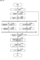
- FIG. 11 is a flowchart showing an example of the procedure of the inference process of the inference model that performs object detection using a captured image as an input.
- step S11 a reset operation of each part of the imaging device 2 is performed.
- step S12 the pixel array unit 101 performs imaging.
- step S13 the DNN processing circuit 126 reads out the captured image (data) from the pixel array unit 101.
- step S14 the DNN processing circuit 126 stores the read captured image in the memory 106.
- step S15 the DNN processing circuit 126 determines whether or not to perform object detection. If the result in step S15 is affirmative, the process proceeds to step S16. If the result in step S15 is negative, the process ends.
- step S16 the DNN processing circuit 126 acquires the captured image from the memory 106 and inputs it to the inference model (neural network), performs object detection by inference processing using the inference model, and outputs the object detection result as the output of the inference model.
- step S17 the DNN processing circuit 126 writes the object detection result back to the memory 106.
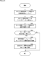
- FIG. 12 is a flowchart showing an example of the procedure of the learning process of the inference model with the captured image as input.
- the DNN processing circuit 126 starts the acquisition process of the learning image.
- the reset operation of each part of the imaging device 2 is performed.
- the pixel array unit 101 performs imaging.
- the DNN processing circuit 126 reads the captured image (data) from the pixel array unit 101.
- the DNN processing circuit 126 stores the read captured image in the memory 106.
- the DNN processing circuit 126 determines whether the acquisition of the learning image has been completed.
- step S36 determines whether the number of captured images required for the learning process of the inference model has been acquired. If the result of step S36 is affirmative, the process proceeds to step S37. If the result of step S36 is negative, the process returns to step S31 and is repeated from step S31.
- step S37 the DNN processing circuit 126 performs a model update process using the backpropagation method using the learning image.
- step S38 the DNN processing circuit 126 generates model parameters at the time of completion of learning.
- step S39 the DNN processing circuit 126 writes the generated model parameters back to the memory 106. When the process of step S39 is completed, the process of this flowchart is completed.
- DNN processing for internal element characteristics As a DNN process for internal element characteristics, an example of the procedure for inference processing and learning processing when feeding back circuit setting values (element control parameters) by inference processing using an inference model for internal element characteristics will be described.
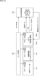
- Example of input and output data for inference processing is a diagram for explaining input/output data of an inference model that uses internal element characteristics as input and feeds back circuit setting values.
- the image pickup device 2 in FIG. 13 includes the pixel array unit 101, the control circuit 104, the memory 106, the monitor circuit 108, and the DNN processing circuit 126 shown in FIG. 8 and FIG. 10.
- the DNN processing circuit 126 reads model parameters from the memory 106 to set (construct) an inference model.
- the monitor circuit 108 detects element characteristic values from the respective probe points of the pixel array unit 101, the control circuit 104, and the memory 106, and supplies them to the DNN processing circuit 126.
- the DNN processing circuit 126 inputs the element characteristic values from the monitor circuit 108 to the inference model.
- the DNN processing circuit 126 supplies circuit setting values (control parameters) output as an inference result of the inference model to the pixel array unit 101, the control circuit 104, and the memory 106.
- the pixel array unit 101, the control circuit 104, and the memory 106 operate according to the circuit setting value from the DNN processing circuit 126.
- the memory 106 can be configured as one memory, or can be configured as two memories, a control value storage memory 106A and a correction target memory 106B.
- the control value storage memory 106A is a memory that stores data for controlling model parameters, circuit setting values, etc.
- the correction target memory 106B is a memory that stores data other than model parameters, such as image data.
- the correction target memory 106B is a target for correction by the circuit setting value of the inference result of the DNN processing circuit 126 when normal data cannot be read due to aging deterioration or failure.
- the memory 106 can be configured by providing areas for the control value storage memory 106A and the correction target memory 106B in one memory.
- the inference model outputs the bias voltage (reference voltage) of the memory read sense amplifier as the circuit setting value of the inference result.
- FIG. 14 is a flowchart showing an example of the procedure of the inference process of the inference model that inputs the internal element characteristics and outputs the circuit setting value.
- the control circuit 104 is configured (set) with the values stored in the memory 106 (control value storage memory 106A).
- the control circuit 104 reads out the known test data stored in the memory 106 (correction target memory 106B).
- the monitor circuit 108 acquires the voltage and temperature information of the probe point as the element characteristic value.
- the processes of steps S52 and S53 can be performed in parallel in synchronization.
- step S54 the control circuit 104 judges whether the test data read out from the memory 106 (correction target memory 106B) is different from the known value. If it is judged in step S54 that the test data is not different from the known value, the process ends. If it is judged in step S54 that the test data is different from the known value, the process proceeds to step S55.
- step S55 the DNN processing circuit 126 inputs the element characteristic value acquired by the monitor circuit 108 into the inference model, and infers a reference voltage (reference voltage of the read circuit of the correction target memory 106B) as a circuit setting value by the inference model.
- step S55 the DNN processing circuit 126 writes the reference voltage value inferred by the inference model back to the memory 106 (control value storage memory 106A), and updates the reference voltage value that the control circuit 104 uses as the circuit setting value next.
- the process of step S55 is completed, the process of this flowchart is completed.
- FIG. 15 is a diagram for explaining input/output data during learning of an inference model that uses internal element characteristics as input and feeds back circuit setting values.
- the DNN processing circuit 126 reads out model parameters from the memory 106 to set (construct) an inference model.
- the monitor circuit 108 detects element characteristic values from the respective probe points of the pixel array unit 101, the control circuit 104, and the memory 106, and supplies them to the DNN processing circuit 126 together with an inference expected value.
- the inference expected value is correct answer data of the output of the inference model in response to the input of the element characteristic value detected from the probe point to the inference model, and an inference expected value corresponding to the element characteristic value is prepared in advance.
- the DNN processing circuit 126 updates the model parameters using the element characteristic value from the monitor circuit 108 and the inference expected value as learning data. After learning, the DNN processing circuit 126 writes the updated model parameters back to the memory 106, and sets the inference model with the model parameters in the inference processing from the next time onwards.
- FIG. 16 is a flowchart showing an example of a procedure of learning processing of an inference model with internal element characteristics as input.
- step S71 a reset operation of each part of the imaging device 2 is performed.
- step S72 the control circuit 104 reads a circuit setting value from the memory 106 (control value storage memory 106A) and configures (sets) the memory 106 (memory 106B to be corrected) with the circuit setting value.
- step S73 the DNN processing circuit 126 writes known test data to the memory 106 (memory 106B to be corrected).
- the DNN processing circuit 126 reads the test data written in the memory 106 (memory 106B to be corrected).
- step S75 the monitor circuit 108 acquires the voltage (including reference voltage, etc.) of the probe point, temperature information, etc. as element characteristic values.
- the processes of steps S74 and S75 can be performed synchronously in parallel.
- step S76 the DNN processing circuit 126 stores the expected read value of the test data (the test data in step S73), the read test data (the test data in step S74), and element characteristic values such as reference voltages (the element characteristic values acquired in step S75) in the memory 106 (control value storage memory 106A) as learning data.
- step S77 the DNN processing circuit 126 determines whether or not to end the acquisition of learning data. If the result is affirmative in step S77, the process proceeds to step S78. If the result is negative in step S77, the process returns to step S72 and repeats from step S72. In step S78, the DNN processing circuit 126 uses the learning data to perform a model update process using the backpropagation method.
- step S79 the DNN processing circuit 126 generates model parameters at the time of completion of learning.
- step S80 the DNN processing circuit 126 writes the generated model parameters back to the memory 106 (control value storage memory 106A).
- DNN processing of captured images and internal element characteristics As DNN processing for a captured image and internal element characteristics, an example of the procedure of inference processing and learning processing when object detection is performed by inference processing using an inference model for a captured image and internal element characteristics will be described.
- FIG. 17 is a diagram for explaining input/output data of an inference model that performs object detection using a captured image and internal element characteristics as input.
- the DNN processing circuit 126 reads model parameters from the memory 106 to set (construct) an inference model.
- the monitor circuit 108 detects element characteristic values from the respective probe points of the pixel array unit 101, the control circuit 104, and the memory 106, and supplies them to the DNN processing circuit 126.
- the memory 106 supplies the captured image captured by the pixel array unit 101 and stored in the memory 106 to the DNN processing circuit 126.
- the DNN processing circuit 126 inputs the element characteristic values from the monitor circuit 108 and the captured image from the memory 106 to the inference model.
- the DNN processing circuit 126 outputs the recognition result, metadata, or corrected image output as the inference result of the inference model to an external system or the like.
- FIG. 18 is a flowchart showing an example of the procedure of an inference process of an inference model that performs object detection using a captured image and internal element characteristics as input.
- step S101 a reset operation of each part of the imaging device 2 is performed.
- step S102 the pixel array unit 101 performs imaging.
- step S103 the DNN processing circuit 126 reads out the captured image (data) from the pixel array unit 101.
- step S104 the DNN processing circuit 126 stores the read captured image in the memory 106.
- the monitor circuit 108 acquires the voltage and temperature information of the probe point as element characteristic values.
- the monitor circuit 108 stores the acquired element characteristic values in the memory 106.
- steps S103 and S105 are started synchronously, and when the processes of both steps S104 and S106 are completed, the process proceeds to step S107.
- step S107 the DNN processing circuit 126 acquires the captured image and the element characteristic value from the memory 106 and inputs them to the inference model (neural network).
- step S108 the DNN processing circuit 126 performs object detection by inference processing using the inference model, and outputs the object detection result as the output of the inference model.
- step S109 the DNN processing circuit 126 writes the object detection result back to the memory 106.
- FIG. 19 is a diagram for explaining input/output data during learning of an inference model that performs image recognition (not limited to object detection) using a captured image and internal element characteristics as input.
- the DNN processing circuit 126 reads out model parameters from the memory 106 to set (construct) an inference model.
- the monitor circuit 108 detects element characteristic values from the respective probe points of the pixel array unit 101, the control circuit 104, and the memory 106, and supplies them to the DNN processing circuit 126.
- the memory 106 supplies the captured image captured by the pixel array unit 101 and stored in the memory 106 to the DNN processing circuit 126.
- the DNN processing circuit 126 performs unsupervised learning of the inference model using the element characteristic values from the monitor circuit 108 and the captured image from the memory 106 as learning data. After learning, the DNN processing circuit 126 writes the updated model parameters back to the memory 106 and sets the inference model with those model parameters in the next inference process.
- FIG. 20 is a flowchart showing an example of a procedure of a learning process of an inference model that performs image recognition using a captured image and internal element characteristics as input.
- step S121 a reset operation of each part of the imaging device 2 is performed.
- step S122 the DNN processing circuit 126 starts acquiring learning data.
- step S123 the pixel array unit 101 performs imaging.
- step S124 the DNN processing circuit 126 reads out the captured image (data) from the pixel array unit 101.
- the DNN processing circuit 126 stores the read captured image in the memory 106.
- the monitor circuit 108 acquires the voltage and temperature information of the probe point as element characteristic values.
- step S127 the monitor circuit 108 stores the acquired element characteristic values in the memory 106. Note that steps S124 and S126 are started synchronously, and when the processes of both steps S125 and S127 are completed, the process proceeds to step S128.
- step S1208 the DNN processing circuit 126 judges whether the acquisition of the learning data is completed. If the result is affirmative in step S128, the process proceeds to step S129. If the result is negative in step S128, the process returns to step S122 and repeats from step S122.
- step S129 the DNN processing circuit 126 acquires the captured image and element characteristic values from the memory 106, inputs them to the inference model (neural network), and performs model update processing by the error backpropagation method.
- step S130 the DNN processing circuit 126 generates model parameters at the time of completion of learning.
- step S131 the DNN processing circuit 126 writes the generated model parameters back to the memory 106 (control value storage memory 106A). When the process of step S131 ends, the process of this flowchart ends.
- ⁇ Learning process execution> (Type 1)
- steps S151 to S156 in FIG. 21 are common to steps S11 to S16 in FIG. 11, and steps S159 to S167 in FIG. 21 are common to steps S31 to S39 in FIG. 12, so the description will be omitted.
- the model parameters in step S167 are written back to the control value storage memory 106A.
- step S157 the DNN processing circuit 126 determines whether the distribution peak of the confidence is equal to or greater than a threshold value as a result of the object detection by the inference model. If the result in step S157 is affirmative, the process proceeds to step S158. If the result in step S157 is negative, the process proceeds to step S159. In step S158, the DNN processing circuit 126 writes the object detection result back to the memory 106. When the process of step S158 ends, the process of this flowchart ends. In steps S159 to S167, a learning process of the inference model is performed, and when the learning is completed, the process of this flowchart ends.
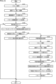
- FIG. 22 shows an example of a procedure for detecting a change in the installation environment (arrangement environment) and determining the learning timing. Note that steps S191 to S199 in FIG. 22 are common to steps S31 to S39 in FIG. 12, so the description will be omitted.
- step S181 a reset operation of each part of the imaging device 2 is performed.
- step S182 the DNN processing circuit 126 acquires temperature information from a temperature sensor outside the imaging device 2.
- the DNN processing circuit 126 stores the acquired temperature information in the memory 106 (control value storage memory 106A).
- the DNN processing circuit 126 acquires ambient luminance information from an external illuminance sensor of the imaging device 2. The ambient luminance information may be acquired from the captured image.
- step S185 the DNN processing circuit 126 stores the acquired luminance information in the memory 106 (control value storage memory 106A).
- step S186 the DNN processing circuit 126 acquires gyro information from a gyro sensor external to the imaging device 2.
- step S187 the DNN processing circuit 126 stores the acquired gyro information in the memory 106 (control value storage memory 106A). Note that steps S182, S184, and S186 are started synchronously, and when all the processes in steps S183, S185, and S187 are completed, the process proceeds to step S188.
- step S188 the DNN processing circuit 126 reads out the environmental information (temperature information, brightness information, gyro information) from the memory 106 (control value storage memory 106A).
- step S189 the DNN processing circuit 126 detects a change in the installation environment (placement environment) of the imaging device 2 based on the environmental information.
- step S190 the DNN processing circuit 126 determines whether the installation location of the imaging device 2 has been changed. If the result in step S190 is affirmative, the processing of this flowchart ends. If the result in step S190 is negative, the processing proceeds to step S191, and in steps S191 to S199, a learning process of the inference model is performed. When the learning is completed, the processing of this flowchart ends. Note that if the memory 106 is divided into the control value storage memory 106A and the correction target memory 106B, the model parameters in step S199 are written back to the control value storage memory 106A.
- the above-mentioned series of processes can be executed by hardware or software.
- the programs constituting the software are installed in a computer.
- the computer includes a computer built into dedicated hardware, and a general-purpose personal computer, for example, capable of executing various functions by installing various programs.
- FIG. 23 is a block diagram showing an example of the hardware configuration of a computer that executes the above-mentioned series of processes using a program.
- a CPU Central Processing Unit
- ROM Read Only Memory
- RAM Random Access Memory
- an input/output interface 505 Connected to the input/output interface 505 are an input unit 506, an output unit 507, a storage unit 508, a communication unit 509, and a drive 510.
- the input unit 506 includes a keyboard, mouse, microphone, etc.
- the output unit 507 includes a display, speaker, etc.
- the storage unit 508 includes a hard disk, non-volatile memory, etc.
- the communication unit 509 includes a network interface, etc.
- the drive 510 drives removable media 511 such as a magnetic disk, optical disk, magneto-optical disk, or semiconductor memory.
- the CPU 501 loads a program stored in the storage unit 508, for example, into the RAM 503 via the input/output interface 505 and the bus 504, and executes the program, thereby performing the above-mentioned series of processes.
- the program executed by the computer (CPU 501) can be provided by being recorded on removable media 511 such as package media, for example.
- the program can also be provided via a wired or wireless transmission medium such as a local area network, the Internet, or digital satellite broadcasting.
- a program can be installed in the storage unit 508 via the input/output interface 505 by inserting the removable media 511 into the drive 510.
- the program can also be received by the communication unit 509 via a wired or wireless transmission medium and installed in the storage unit 508.
- the program can be pre-installed in the ROM 502 or storage unit 508.
- the program executed by the computer may be a program in which processing is performed chronologically in the order described in this specification, or a program in which processing is performed in parallel or at the required timing, such as when called.
- the processing performed by a computer according to a program does not necessarily have to be performed in chronological order according to the order described in the flowchart.
- the processing performed by a computer according to a program also includes processing that is executed in parallel or individually (for example, parallel processing or processing by objects).
- the program may be processed by one computer (processor), or may be distributed among multiple computers. Furthermore, the program may be transferred to a remote computer for execution.
- a system refers to a collection of multiple components (devices, modules (parts), etc.), regardless of whether all the components are in the same housing. Therefore, multiple devices housed in separate housings and connected via a network, and a single device in which multiple modules are housed in a single housing, are both systems.
- the configuration described above as one device (or processing unit) may be divided and configured as multiple devices (or processing units).
- the configurations described above as multiple devices (or processing units) may be combined and configured as one device (or processing unit).
- configurations other than those described above may also be added to the configuration of each device (or processing unit).
- part of the configuration of one device (or processing unit) may be included in the configuration of another device (or other processing unit).
- this technology can be configured as cloud computing, in which a single function is shared and processed collaboratively by multiple devices via a network.
- the above-mentioned program can be executed in any device.
- the device has the necessary functions (functional blocks, etc.) and is able to obtain the necessary information.
- each step described in the above flowchart can be executed by one device, or can be shared and executed by multiple devices.
- one step includes multiple processes, the multiple processes included in that one step can be executed by one device, or can be shared and executed by multiple devices.
- multiple processes included in one step can be executed as multiple step processes.
- processes described as multiple steps can be executed collectively as one step.
- processing of the steps that describe a program executed by a computer may be executed chronologically in the order described in this specification, or may be executed in parallel, or individually at the required timing, such as when a call is made. In other words, as long as no contradictions arise, the processing of each step may be executed in an order different from the order described above. Furthermore, the processing of the steps that describe this program may be executed in parallel with the processing of other programs, or may be executed in combination with the processing of other programs.
- the present technology can also be configured as follows.
- the processing unit performs a learning process of an inference model used in the inference process.
- the imaging device according to any one of (10) to (13), wherein the processing unit performs the inference process using an image captured by the imaging unit and the element characteristic value as input.
- the processing unit performs image recognition on the captured image by the inference processing.
- the processing unit performs a learning process of an inference model used in the inference process.
- the imaging device according to any one of (10) to (16), wherein the imaging unit and the processing unit are mounted on an integrated chip.
- Imaging device 101 Pixel array section, 104 Control circuit, 105 Signal processing circuit, 108 Memory, 126 DNN circuit
Landscapes
- Engineering & Computer Science (AREA)
- Multimedia (AREA)
- Theoretical Computer Science (AREA)
- Signal Processing (AREA)
- Computer Vision & Pattern Recognition (AREA)
- Physics & Mathematics (AREA)
- General Physics & Mathematics (AREA)
- Evolutionary Computation (AREA)
- Health & Medical Sciences (AREA)
- Artificial Intelligence (AREA)
- Computing Systems (AREA)
- Databases & Information Systems (AREA)
- General Health & Medical Sciences (AREA)
- Medical Informatics (AREA)
- Software Systems (AREA)
- Studio Devices (AREA)
Abstract
Description
スマートフォンや監視カメラ等のデバイスにおいて、イメージセンサで取得された画像に対して、機械学習技術を用いて物体検出や認識処理等の推論処理を行う機能を持つものが多く発売されている。また、より発展的な機能として、取得された画像を用いて、対象の推論モデルの学習を行うものも学会等で多く提案がなされている。
近年のイメージセンサにおいては有機膜の活用や、MRAM(Magnetoresistive Random Access Memory:磁気抵抗メモリ)等の新規不揮発メモリデバイスの活用が進んでいる。これらのデバイスにおいて、製造時の特性ばらつきの補正や、使用中の特性変化への対応が課題となる。
(1)撮像画像に対する推論処理
(2)撮像画像を用いた学習処理
(3)内部素子特性に対する推論処理
(4)内部素子特性を用いた学習処理
(5)撮像画像と内部素子特性の両方に対する推論処理
(6)撮像画像と内部素子特性の両方を用いた学習処理
<本技術が適用されたデジタルカメラの一実施の形態>
図2は、図1の撮像装置2の基本的構成例を示すブロック図である。図2において、撮像装置2は、撮像ブロック20及び信号処理ブロック30を有する。撮像ブロック20と信号処理ブロック30とは、接続線(内部バス)CL1,CL2、及び、CL3によって電気的に接続されている。
図6を用いて撮像装置2におけるDNN処理について説明する。撮像装置2におけるDNN処理は図2の信号処理ブロック30により実施され、信号処理ブロック30には、撮像部21からの撮像画像と、後述のモニタ回路からの撮像装置2の内部素子特性(内部素子特性を示す素子特性値)とが入力され得る。信号処理ブロック30は、次の(1)ないし(4)のようなDNN処理を行うことができる。
撮像装置2におけるDNN処理としては、畳み込みニューラルネットワーク(CNN:Convolutional Neural Network)、Generative Adversarial Network(GAN)、Transformer技術等の機械学習の技術を用いたDNN処理(推論処理)によるオブジェクト検出やセグメンテーション等の画像認識、画像圧縮や高解像度化(超解像)等の各種加工画像の生成等が実施され得る。この場合、DNN処理で用いられる推論モデルへの入力は、図6のように撮像部21において取得された撮像画像であり、推論モデルからの出力はDNN処理により加工された画像(補正画像)、メタデータ(推論結果)のみ、または、これらの両方が考えられる。以下において、DNN処理に用いられる推論モデルを、単に推論モデルともいう。
撮像装置2におけるDNN処理としては、撮像装置2を構成する様々な素子の異常の検出や、撮像装置2の内部回路にフィードバックする適切な回路設定値(撮像装置2の各モジュールに供給されるコア電源電圧やバイアス電圧/電流等)の推定等が実施され得る。この場合、推論モデルへの入力は、図6のように撮像装置2を構成する素子の特性(内部素子特性)である。内部素子特性を示す値(素子特性値)は、撮像装置2の内部に配置されたモニタ回路から取得され得る。推論モデルからの出力は、回路設定値、異常検出(の結果)、または、これらの両方が考えられる。
ここで、推論モデルに入力される素子特性値には、次のような例が該当する。なお、推論モデルに入力される素子特性値は1または任意の組合せの複数種の素子特性値であってよい。
・メモリデバイス(メモリ33)における、各ワード読み出し時の信号線電圧、電源ノイズ、周囲の環境情報(温度、ジャイロ等)
・各ブロック単位での供給電圧、消費電流波形(特に、低電力化技術としてDynamic Voltage and Frequency Scaling(DVFS)技術を適用した際の電源波形や消費電流値)
推論モデルから出力される回路設定値(制御パラメータ)には、次のような例が該当する。推論モデルから出力される回路設定値は1または任意の組合せの複数種の回路設定値であってよい。
・メモリ読み出し回路におけるセンスアンプ用参照電圧値
・画素駆動タイミング(トリガパルスタイミング、立ち上がり幅等)
有機材料を用いたセンサデバイスにおいて、センサに対して強い光が当たった際の劣化が課題となるが、これに対して、センサ読み出し時の各カラムの信号電圧等をモニタリングし、推論モデルへの入力することで、現在の劣化状況に合わせた画素負バイアスの制御、負荷MOS電流量の制御、読み出しパルス幅の制御等を行うことができる。
撮像装置2におけるDNN処理としては、(1)と同様にDNN処理による画像認識、補正画像の生成等が実施され得る。ただし、(1)の場合と異なり、推論モデルへの入力は、撮像画像と内部素子特性との両方であり、推論モデルからの出力は、補正画像、メタデータ(推論結果)、または、これらの両方である。推論モデルに対して、撮像画像だけでなく、内部素子特性が入力されることで、素子ごとのばらつきや特性変化が加味されて、より高い精度の画像認識や加工画像の生成が可能になる。
画素アレイ部に対するセンサ読み出し時、各カラム回路における負荷MOSトランジスタの電流値をモニタリングし、推論モデルへの入力とすることで、リニアリティ特性の変化を含めたような形で撮像画像に対する推論処理を行うことができる。
撮像装置2におけるDNN処理としては、上記(1)ないし(4)のいずれが実施される場合においても、推論モデルの学習処理(更新処理)、すなわち、推論モデルのパラメータ(重み係数・バイアス等)の更新が実施され得る。例えば、推論モデルの学習処理としては、誤差逆伝播法が採用され得る。この場合に、撮像装置2の内部のメモリに撮像画像や素子特性値が学習データとして保存され、保存された学習データを用いて、推論モデルの最適なパラメータが誤差逆伝播法により算出される。学習処理後の推論モデルのパラメータは、その算出された最適なパラメータに更新される。
本技術の撮像装置2では、推論モデルの学習処理を行うタイミング(学習タイミング)がオンチップで決定され得る。学習タイミングの決定方法としては、例えば次のような方法が適用され得る。なお、推論モデルの学習処理に使用される撮像画像等の学習データ(教師データ)を新たに取得する場合には、学習処理には、学習データを取得(収集)する処理が含まれることとし、学習タイミングは、学習データの取得を開始するタイミングであることとする。
撮像装置2は、内部回路の適切な回路設定値を推論して内部回路にフィードバックするDNN処理(回路設定値の更新処理)を実施する場合において、回路設定値の更新処理に関する情報、すなわち、回路設定値がどのように推論、判断されたかを示す情報を履歴(ログ)として保存し、出力する機構(機能)を有するようにしてもよい。ログは、DNN処理による回路設定値の更新処理が実行された際に撮像装置2のメモリ33に保存され、外部装置からの要求時等に外部装置へ出力される。図7は、DNN処理による回路設定値の更新処理に関するログの一例を示した図である。図7において、ログの情報として、実行番号、処理コード、タイムスタンプ、入力情報(不図示)、および、処理結果等の情報が含まれる。実行番号は、回路設定値の更新処理に対して、実行された順序を示す順番である。処理コードは、回路設定値の更新処理の実行毎に割り振られたコードである。タイムスタンプは、回路設定値の変更処理が実行された時刻である。入力情報は、回路設定値の更新処理の際にDNN処理(推論モデル)に入力された内部素子特性(素子特性値)である。処理結果は、回路設定値の更新処理により更新された回路設定値である、図7には更新された回路設定値の例として、素子xxxのバイアス電圧の設定値、素子yyyの切り替えスイッチの設定値、素子zzzへのクロック周波数の設定値が示されている。
一般に推論モデルの学習処理においては、事前に用意された入力データの推論モデルへの入力に対して、推論モデルから出力される出力データと、推論モデルからの出力としてあるべきラベル(正解データ)とを対応付け、それらの間の誤差を最小化する推論モデルのパラメータを求める学習処理が行われる。
図8は、本技術が適用された撮像装置2の実施の形態の構成例を示したブロック図である。図8には、図2乃至図5には図示されていない撮像装置2の構成要素が示されると共に、図2乃至図5の一部の構成要素を具体化又は抽象化した構成要素が示されている。
図9は、撮像装置2の他の実施の形態の構成例を示したブロック図である。図中、図8の撮像装置2と共通する部分には同一の符号が付されており、その説明を適宜省略する。
図8のモニタ回路108、および図9のモニタ回路108Aないし108G(以下、全てを総称してモニタ回路108という)は、具体例として、参照文献1(特開2018-101966号公報)、参照文献2(特開2006-202383号公報)、参照文献3(特開2021-67473号公報)、および、参照文献4(T. Hashida, et al., “An On-Chip Waveform Capturer and Application to Diagnosis of Power Delivery in SoC Integration,” Journal of Solid-State Circuits, vol.46, No.4, Apr. 2011.)に記載の技術が適用され得る。
図10は、撮像装置の積層型センサとしての回路構成例を示した図である。
なお、積層型チップとしての撮像装置2の構成例は、図3ないし図5に示されており、図10は、図3の構成例における回路単位での配置例を例示した図である。図10において、撮像装置2は、上側のダイ51と下側のダイ52とが積層されて1つの積層型チップとして構成される。ダイ51は、画素アレイ部101が搭載された画素チップであり、ダイ52は、撮像装置2の画像アレイ部101以外が搭載された回路チップである。ダイ51とダイ52との間を接続する配線は、ダイ51の接続部111Aおよび112Aと、これらに対向するダイ51の接続部111Bおよび112Bとの間に配置される。ダイ51の画素アレイ部101には、各画素の受光素子には例えばR(レッド)、G(グリーン)、B(ブルー)の原色からなる図中(A)ないし(C)のようなベイヤー配列のカラーフィルタが設置される。図中(A)ないし(C)は、それぞれ、1画素ごと、隣接する4画素ごと、および隣接する9画素ごとにRGBのフィルタがベイヤー配列で配置されたカラーフィルタである。また、各画素の受光素子に設置されるフィルタは、図中(D)のような4色のカラーフィルタの場合や、IR透過フィルタ、偏光フィルタ、または補色フィルタ等の場合であってもよく、特に限定されない。
<撮像画像に対するDNN処理>
撮像画像に対するDNN処理として、撮像画像に対して推論モデルによる推論処理により、物体検出を行う場合の推論処理および学習処理の手順例について説明する。なお、以下の図11ないし図22は、図8の構成の撮像装置2に基づいて説明を行うが、図8の信号処理回路105の処理については、図10のDNN処理回路126が行うものとする。
図11は、撮像画像を入力として物体検出を行う推論モデルの推論処理の手順例を示したフローチャートである。ステップS11では、撮像装置2の各部のリセット動作が行われる。ステップS12では、画素アレイ部101は、撮像を行う。ステップS13では、DNN処理回路126は、画素アレイ部101から撮像画像(データ)を読み出す。ステップS14では、DNN処理回路126は、読み出した撮像画像をメモリ106に記憶させる。ステップS15では、DNN処理回路126は、物体検出を行うか否かを判定する。ステップS15において、肯定された場合には処理はステップS16に進む。ステップS15において、否定された場合には処理は終了する。ステップS16では、DNN処理回路126は、メモリ106から撮像画像を取得して推論モデル(ニューラルネットワーク)への入力とし、推論モデルによる推論処理により物体検出を行い、推論モデルの出力として物体検出結果を出力する。ステップS17では、DNN処理回路126は、物体検出結果をメモリ106に書き戻す。ステップS17の処理が終了すると、本フローチャートの処理が終了する。
図12は、撮像画像を入力とする推論モデルの学習処理の手順例を示したフローチャートである。ステップS31では、DNN処理回路126は、学習用画像の取得処理を開始する。ステップS32では、撮像装置2の各部のリセット動作が行われる。ステップS33では、画素アレイ部101は、撮像を行う。ステップS34では、DNN処理回路126は、画素アレイ部101から撮像画像(データ)を読み出す。ステップS35では、DNN処理回路126は、読み出した撮像画像をメモリ106に記憶させる。ステップS36では、DNN処理回路126は、学習用画像の取得は終了したか否かを判定する。すなわち、DNN処理回路126は、推論モデルの学習処理に必要な数の撮像画像が取得されたか否かを判定する。ステップS36において、肯定された場合には処理はステップS37に進む。ステップS36において、否定された場合には処理はステップS31に戻り、ステップS31から繰り返す。ステップS37では、DNN処理回路126は、学習用画像を使用して、誤差逆伝播法を用いたモデル更新処理を行う。ステップS38では、DNN処理回路126は、学習完了時のモデルパラメータを生成する。ステップS39では、DNN処理回路126は、生成したモデルパラメータをメモリ106に書き戻す。ステップS39の処理が終了すると、本フローチャートの処理が終了する。
内部素子特性に対するDNN処理として、内部素子特性に対して推論モデルによる推論処理により、回路設定値(素子制御パラメータ)をフォードバックする場合の推論処理および学習処理の手順例について説明する。
図13は、内部素子特性を入力として回路設定値をフィードバックする推論モデルの入出力データに関して説明する図である。図13の撮像装置2には、図8及び図10に示した画素アレイ部101、制御回路104、メモリ106、モニタ回路108、およびDNN処理回路126が示されている。DNN処理回路126は、メモリ106からモデルパラメータを読み出して推論モデルを設定(構築)する。モニタ回路108は、画素アレイ部101、制御回路104、およびメモリ106のそれぞれのプローブ点から素子特性値を検出し、DNN処理回路126に供給する。DNN処理回路126は、モニタ回路108からの素子特性値を推論モデルへの入力とする。DNN処理回路126は、推論モデルの推論結果として出力された回路設定値(制御パラメータ)を画素アレイ部101、制御回路104、メモリ106に供給する。画素アレイ部101、制御回路104、およびメモリ106は、DNN処理回路126からの回路設定値にしたがって動作する。なお、メモリ106は、1つのメモリで構成する他、制御値格納メモリ106A及び補正対象メモリ106Bの2つのメモリに分けて構成することができる。制御値格納メモリ106Aは、モデルパラメータや回路設定値等の制御のためのデータを記憶するメモリである。補正対象メモリ106Bは、モデルパラメータ等以外のデータ、例えば、画像データ等を記憶するメモリである。補正対象メモリ106Bは、経年劣化や故障等により正常なデータ読み出しが出来なくなった場合に、DNN処理回路126の推論結果の回路設定値によって、補正の対象となる。その他、メモリ106は、1つのメモリに、制御値格納メモリ106A及び補正対象メモリ106Bそれぞれとしての領域を設けて構成することができる。
図14は、内部素子特性を入力として回路設定値を出力する推論モデルの推論処理の手順例を示したフローチャートである。ステップS51では、メモリ106(制御値格納メモリ106A)に記憶されている値で、制御回路104のコンフィグレーション(設定)が行われる。ステップS52では、制御回路104は、メモリ106(補正対象メモリ106B)に記憶されている既知のテスト用データを読み出す。ステップS53では、モニタ回路108は、プローブ点の電圧や温度情報等を素子特性値として取得する。ここで、ステップS52及びS53の処理は同期して並列に行うことができる。ステップS54では、制御回路104は、メモリ106(補正対象メモリ106B)から読み出されたテスト用データが既知の値と異なるかどうかを判定する。ステップS54において、テスト用データが既知の値と異ならないと判定された場合、処理は終了する。ステップS54において、テスト用データが既知の値と異なると判定された場合、処理は、ステップS55に進む。ステップS55では、DNN処理回路126は、モニタ回路108で取得された素子特性値を推論モデルに入力し、推論モデルにより回路設定値として参照電圧(補正対象メモリ106Bの読み出し回路の参照電圧)等を推論する。ステップS55では、DNN処理回路126は、推論モデルにより推論された参照電圧値をメモリ106(制御値格納メモリ106A)に書き戻し、制御回路104が次に回路設定値として使用する参照電圧値を更新する。ステップS55の処理が終了すると、本フローチャートの処理が終了する。
図15は、内部素子特性を入力として回路設定値をフィードバックする推論モデルの学習時の入出力データに関して説明する図である。尚、図中、図13と共通する部分には、同一符号が付されており、その説明を省略する。DNN処理回路126は、メモリ106からモデルパラメータを読み出して推論モデルを設定(構築)する。モニタ回路108は、画素アレイ部101、制御回路104、およびメモリ106のそれぞれのプローブ点から素子特性値を検出し、推論期待値と共にDNN処理回路126に供給する。推論期待値は、プローブ点から検出された素子特性値の推論モデルへの入力に対する推論モデルの出力の正解データであり、素子特性値に対応した推論期待値が事前に用意されている。DNN処理回路126は、モニタ回路108からの素子特性値と、推論期待値とを学習用データとして使用してモデルパラメータを更新する。DNN処理回路126は、学習後、更新されたモデルパラメータをメモリ106に書き戻し、次回からの推理処理においてそのモデルパラメータで推論モデルを設定する。
図16は、内部素子特性を入力とする推論モデルの学習処理の手順例を示したフローチャートである。ステップS71では、撮像装置2の各部のリセット動作が行われる。ステップS72では、制御回路104は、メモリ106(制御値格納メモリ106A)から回路設定値を読み出し、その回路設定値で、メモリ106(補正対象メモリ106B)のコンフィグレーション(設定)を行う。ステップS73では、DNN処理回路126は、メモリ106(補正対象メモリ106B)に既知のテスト用データを書き込む。ステップS74では、DNN処理回路126は、メモリ106(補正対象メモリ106B)に書き込んだテスト用データを読み出す。ステップS75では、モニタ回路108は、プローブ点の電圧(参照電圧等を含む)や温度情報等を素子特性値として取得する。ここで、ステップS74及びS75の処理は同期して並列に行うことができる。ステップS76では、DNN処理回路126は、テスト用データの読み出し期待値(ステップS73のテスト用データ)と、読み出したテスト用データ(ステップS74のテスト用データ)と、参照電圧等の素子特性値(ステップS75で取得された素子特性値)とを学習用データとしてメモリ106(制御値格納メモリ106A)に記憶させる。
撮像画像および内部素子特性に対するDNN処理として、撮像画像および内部素子特性に対して推論モデルによる推論処理により、物体検出を行う場合の推論処理および学習処理の手順例について説明する。
図17は、撮像画像および内部素子特性を入力として物体検出を行う推論モデルの入出力データに関して説明する図である。尚、図中、図15と共通する部分には、同一符号が付されており、その説明を省略する。DNN処理回路126は、メモリ106からモデルパラメータを読み出して推論モデルを設定(構築)する。モニタ回路108は、画素アレイ部101、制御回路104、およびメモリ106のそれぞれのプローブ点から素子特性値を検出し、DNN処理回路126に供給する。メモリ106は、画素アレイ部101により撮像されてメモリ106に記憶された撮像画像をDNN処理回路126に供給する。DNN処理回路126は、モニタ回路108からの素子特性値と、メモリ106からの撮像画像とを推論モデルへの入力とする。DNN処理回路126は、推論モデルの推論結果として出力された認識結果、メタデータ、または補正画像を外部システム等に出力する。
図18は、撮像画像および内部素子特性を入力として物体検出を行う推論モデルの推論処理の手順例を示したフローチャートである。ステップS101では、撮像装置2の各部のリセット動作が行われる。ステップS102では、画素アレイ部101は、撮像を行う。ステップS103では、DNN処理回路126は、画素アレイ部101から撮像画像(データ)を読み出す。ステップS104では、DNN処理回路126は、読み出した撮像画像をメモリ106に記憶させる。ステップS105では、モニタ回路108は、プローブ点の電圧や温度情報等を素子特性値として取得する。ステップS106では、モニタ回路108は、取得した素子特性値をメモリ106に記憶させる。なお、ステップS103とステップS105は同期して開始され、ステップS104とステップS106の両方の処理が終了すると、処理はステップS107に進む。
ステップS107では、DNN処理回路126は、メモリ106から撮像画像と素子特性値とを取得して推論モデル(ニューラルネットワーク)に入力する。ステップS108では、DNN処理回路126は、推論モデルによる推論処理により物体検出を行い、推論モデルの出力として物体検出結果を出力する。ステップS109では、DNN処理回路126は、物体検出結果をメモリ106に書き戻す。ステップS109の処理が終了すると、本フローチャートの処理が終了する。
図19は、撮像画像および内部素子特性を入力として画像認識(物体検出に限らない)を行う推論モデルの学習時の入出力データに関して説明する図である。尚、図中、図15と共通する部分には、同一符号が付されており、その説明を省略する。DNN処理回路126は、メモリ106からモデルパラメータを読み出して推論モデルを設定(構築)する。モニタ回路108は、画素アレイ部101、制御回路104、およびメモリ106のそれぞれのプローブ点から素子特性値を検出し、DNN処理回路126に供給する。メモリ106は、画素アレイ部101により撮像されてメモリ106に記憶された撮像画像をDNN処理回路126に供給する。DNN処理回路126は、モニタ回路108からの素子特性値と、メモリ106からの撮像画像とを学習用データとして用いて推論モデルの教師無しの学習を行う。DNN処理回路126は、学習後、更新されたモデルパラメータをメモリ106に書き戻し、次回からの推理処理においてそのモデルパラメータで推論モデルを設定する。
図20は、撮像画像および内部素子特性を入力として画像認識を行う推論モデルの学習処理の手順例を示したフローチャートである。ステップS121では、撮像装置2の各部のリセット動作が行われる。ステップS122では、DNN処理回路126は学習用データの取得を開始する。ステップS123では、画素アレイ部101は、撮像を行う。ステップS124では、DNN処理回路126は、画素アレイ部101から撮像画像(データ)を読み出す。ステップS125では、DNN処理回路126は、読み出した撮像画像をメモリ106に記憶させる。ステップS126では、モニタ回路108は、プローブ点の電圧や温度情報等を素子特性値として取得する。ステップS127では、モニタ回路108は、取得した素子特性値をメモリ106に記憶させる。なお、ステップS124とステップS126は同期して開始され、ステップS125とステップS127の両方の処理が終了すると、処理はステップS128に進む。
ステップS131の処理が終了すると、本フローチャートの処理が終了する。
(形態1)
撮像画像に含まれる物体検出する推論処理において、推論結果から学習タイミングを判断する処理の手順例を図21のフローチャートに示す。なお、図21のステップS151ないしステップS156は、図11のステップS11ないしステップS16と共通し、図21のステップS159ないしステップS167は、図12のステップS31ないしステップS39と共通するので説明を省略する。なお、メモリ106が、制御値格納メモリ106Aと補正対象メモリ106Bとに別れている場合、ステップS167のモデルパラメータを書き戻しは、制御値格納メモリ106Aに対して行われる。ステップS157では、DNN処理回路126は、推論モデルによる物体検出の結果、確信度の分布ピークが閾値以上か否かを判定する。ステップS157において、肯定された場合には処理はステップS158に進む。ステップS157において、否定された場合には処理はステップS159に進む。ステップS158では、DNN処理回路126は、物体検出結果をメモリ106に書き戻す。ステップS158の処理が終了すると、本フローチャートの処理が終了する。ステップS159ないしステップS167では推論モデルの学習処理が行われて、学習が完了すると、本フローチャートの処理が終了する。
設置環境(配置環境)の変化を検出して学習タイミングを判断する処理の手順例を図22に示す。なお、図22のステップS191ないしステップS199は、図12のステップS31ないしステップS39と共通するので説明を省略する。ステップS181では、撮像装置2の各部のリセット動作が行われる。ステップS182では、DNN処理回路126は、撮像装置2の外部の温度センサから温度情報を取得する。ステップS183では、DNN処理回路126は、取得した温度情報をメモリ106(制御値格納メモリ106A)に記憶させる。ステップS184では、DNN処理回路126は、撮像装置2の外部の照度センサから周辺輝度情報を取得する。周辺輝度情報は、撮像画像から取得してもよい。ステップS185では、DNN処理回路126は、取得した輝度情報をメモリ106(制御値格納メモリ106A)に記憶させる。ステップS186では、DNN処理回路126は、撮像装置2の外部のジャイロセンサからジャイロ情報を取得する。ステップS187では、DNN処理回路126は、取得したジャイロ情報をメモリ106(制御値格納メモリ106A)に記憶させる。なお、ステップS182とステップS184とステップS186は同期して開始され、ステップS183とステップS185とステップS187の全ての処理が終了すると、処理はステップS188に進む。
上述した一連の処理は、ハードウエアにより実行することもできるし、ソフトウエアにより実行することもできる。一連の処理をソフトウエアにより実行する場合には、そのソフトウエアを構成するプログラムが、コンピュータにインストールされる。ここで、コンピュータには、専用のハードウエアに組み込まれているコンピュータや、各種のプログラムをインストールすることで、各種の機能を実行することが可能な、例えば汎用のパーソナルコンピュータなどが含まれる。
なお、本技術は以下のような構成も取ることができる。
(1)
画像を撮像する撮像部と、
一体化されたチップに前記撮像部とともに搭載された処理部であって、前記撮像部が撮像した撮像画像を入力とした推論処理を行う処理部と
を有し、
前記処理部は、前記推論処理に用いられる推論モデルの学習処理を行う
撮像装置。
(2)
前記推論モデルは、機械学習技術におけるニューラルネットワークの構造を有する
前記(1)に記載の撮像装置。
(3)
前記処理部は、前記撮像部が撮像した前記撮像画像を用いて前記学習処理を行う
前記(1)又は(2)に記載の撮像装置。
(4)
前記処理部は、誤差逆伝播法を用いて前記学習処理を行う
前記(1)乃至(3)のいずれかに記載の撮像装置。
(5)
前記処理部は、前記学習処理を行う学習タイミングを決定する
前記(1)乃至(4)のいずれかに記載の撮像装置。
(6)
前記処理部は、環境情報に基づいて前記推論処理により出力される各クラスの確信度に基づいて前記学習タイミングを決定する
前記(5)に記載の撮像装置。
(7)
前記処理部は、前記チップに搭載された素子の特性を示す素子特性値に基づいて前記学習タイミングを決定する
前記(5)又は(6)に記載の撮像装置。
(8)
前記処理部は、前記素子特性値の変化に基づいて前記学習タイミングを決定する
前記(7)に記載の撮像装置。
(9)
前記処理部は、前記推論処理により前記撮像画像に対する画像認識を行う
前記(1)乃至(8)のいずれかに記載の撮像装置。
(10)
画像を撮像する撮像部と、
推論処理を行う処理部と
を有し、
前記処理部は、素子の特性を示す素子特性値を入力として前記推論処理を行う
撮像装置。
(11)
前記処理部は、前記推論処理の推論結果として、回路の動作にかかわる回路設定値を出力する
前記(10)に記載の撮像装置。
(12)
前記処理部は、前記素子特性値として、前記撮像部の画素アレイ、制御回路、および、記憶素子のうちのいれかの素子特性値を取得する
前記(10)又は(11)に記載の撮像装置。
(13)
前記処理部は、前記素子特性値として、電流値、電圧値、及び、温度情報のうちのいずれかを取得する
前記(10)乃至(12)のいずれかに記載の撮像装置。
(14)
前記処理部は、前記撮像部が撮像した撮像画像と前記素子特性値とを入力として前記推論処理を行う
前記(10)乃至(13)のいずれかに記載の撮像装置。
(15)
前記処理部は、前記推論処理により前記撮像画像に対する画像認識を行う
前記(14)に記載の撮像装置。
(16)
前記処理部は、前記推論処理に用いられる推論モデルの学習処理を行う
前記(10)乃至(15)のいずれかに記載の撮像装置。
(17)
前記撮像部と前記処理部とは一体化されたチップに搭載された
前記(10)乃至(16)のいずれかに記載の撮像装置。
(18)
撮像部と、
一体化されたチップに前記撮像部とともに搭載された処理部と
を有するデータ処理装置の
前記撮像部が、画像を撮像し、
前記処理部が、前記撮像部が撮像した撮像画像を入力とした推論処理を行い、かつ、前記推論処理に用いられる推論モデルの学習処理を行う
データ処理方法。
(19)
コンピュータを
画像を撮像する撮像部とともに一体化されたチップに搭載された処理部であって、前記撮像部が撮像した撮像画像を入力とした推論処理を行い、かつ、前記推論処理に用いられる推論モデルの学習処理を行う処理部
として機能させるためのプログラムが記録された記録媒体。
Claims (19)
- 画像を撮像する撮像部と、
一体化されたチップに前記撮像部とともに搭載された処理部であって、前記撮像部が撮像した撮像画像を入力とした推論処理を行う処理部と
を有し、
前記処理部は、前記推論処理に用いられる推論モデルの学習処理を行う
撮像装置。 - 前記推論モデルは、機械学習技術におけるニューラルネットワークの構造を有する
請求項1に記載の撮像装置。 - 前記処理部は、前記撮像部が撮像した前記撮像画像を用いて前記学習処理を行う
請求項1に記載の撮像装置。 - 前記処理部は、誤差逆伝播法を用いて前記学習処理を行う
請求項1に記載の撮像装置。 - 前記処理部は、前記学習処理を行う学習タイミングを決定する
請求項1に記載の撮像装置。 - 前記処理部は、環境情報に基づいて前記推論処理により出力される各クラスの確信度に基づいて前記学習タイミングを決定する
請求項5に記載の撮像装置。 - 前記処理部は、前記チップに搭載された素子の特性を示す素子特性値に基づいて前記学習タイミングを決定する
請求項5に記載の撮像装置。 - 前記処理部は、前記素子特性値の変化に基づいて前記学習タイミングを決定する
請求項7に記載の撮像装置。 - 前記処理部は、前記推論処理により前記撮像画像に対する画像認識を行う
請求項1に記載の撮像装置。 - 画像を撮像する撮像部と、
推論処理を行う処理部と
を有し、
前記処理部は、素子の特性を示す素子特性値を入力として前記推論処理を行う
撮像装置。 - 前記処理部は、前記推論処理の推論結果として、回路の動作にかかわる回路設定値を出力する
請求項10に記載の撮像装置。 - 前記処理部は、前記素子特性値として、前記撮像部の画素アレイ、制御回路、および、記憶素子のうちのいずれかの素子特性値を取得する
請求項10に記載の撮像装置。 - 前記処理部は、前記素子特性値として、電流値、電圧値、及び、温度情報のうちのいずれかを取得する
請求項10に記載の撮像装置。 - 前記処理部は、前記撮像部が撮像した撮像画像と前記素子特性値とを入力として前記推論処理を行う
請求項10に記載の撮像装置。 - 前記処理部は、前記推論処理により前記撮像画像に対する画像認識を行う
請求項14に記載の撮像装置。 - 前記処理部は、前記推論処理に用いられる推論モデルの学習処理を行う
請求項10に記載の撮像装置。 - 前記撮像部と前記処理部とは一体化されたチップに搭載された
請求項10に記載の撮像装置。 - 撮像部と、
一体化されたチップに前記撮像部とともに搭載された処理部と
を有するデータ処理装置の
前記撮像部が、画像を撮像し、
前記処理部が、前記撮像部が撮像した撮像画像を入力とした推論処理を行い、かつ、前記推論処理に用いられる推論モデルの学習処理を行う
データ処理方法。 - コンピュータを
画像を撮像する撮像部とともに一体化されたチップに搭載された処理部であって、前記撮像部が撮像した撮像画像を入力とした推論処理を行い、かつ、前記推論処理に用いられる推論モデルの学習処理を行う処理部
として機能させるためのプログラムが記録された記録媒体。
Priority Applications (1)
| Application Number | Priority Date | Filing Date | Title |
|---|---|---|---|
| CN202480009465.5A CN120604276A (zh) | 2023-02-03 | 2024-01-18 | 成像装置、数据处理方法及记录介质 |
Applications Claiming Priority (2)
| Application Number | Priority Date | Filing Date | Title |
|---|---|---|---|
| JP2023015027 | 2023-02-03 | ||
| JP2023-015027 | 2023-02-03 |
Publications (1)
| Publication Number | Publication Date |
|---|---|
| WO2024162015A1 true WO2024162015A1 (ja) | 2024-08-08 |
Family
ID=92146411
Family Applications (1)
| Application Number | Title | Priority Date | Filing Date |
|---|---|---|---|
| PCT/JP2024/001199 Ceased WO2024162015A1 (ja) | 2023-02-03 | 2024-01-18 | 撮像装置、データ処理方法、及び、記録媒体 |
Country Status (2)
| Country | Link |
|---|---|
| CN (1) | CN120604276A (ja) |
| WO (1) | WO2024162015A1 (ja) |
Citations (8)
| Publication number | Priority date | Publication date | Assignee | Title |
|---|---|---|---|---|
| JP2001054027A (ja) * | 1999-08-16 | 2001-02-23 | Nikon Corp | デジタルスチルカメラ |
| JP2008182419A (ja) * | 2007-01-24 | 2008-08-07 | Matsushita Electric Ind Co Ltd | 位相調整装置およびデジタルカメラ |
| KR20180138558A (ko) * | 2018-10-10 | 2018-12-31 | 에스케이텔레콤 주식회사 | 객체 검출을 위한 영상분석 서버장치 및 방법 |
| JP2020182219A (ja) * | 2018-07-31 | 2020-11-05 | ソニーセミコンダクタソリューションズ株式会社 | 固体撮像装置、電子機器及び制御方法 |
| JP2021122106A (ja) * | 2020-01-31 | 2021-08-26 | キヤノン株式会社 | 撮像装置、学習装置、撮像装置の制御方法、学習方法、学習済みモデルおよびプログラム |
| WO2021187365A1 (ja) * | 2020-03-19 | 2021-09-23 | ソニーセミコンダクタソリューションズ株式会社 | データ生成方法、学習方法、推定方法、データ生成装置及びプログラム |
| WO2022070947A1 (ja) * | 2020-09-30 | 2022-04-07 | ソニーセミコンダクタソリューションズ株式会社 | 信号処理装置、撮像装置、信号処理方法 |
| JP2022128256A (ja) * | 2021-02-22 | 2022-09-01 | 株式会社日立製作所 | 異常度算出システムおよび方法 |
-
2024
- 2024-01-18 WO PCT/JP2024/001199 patent/WO2024162015A1/ja not_active Ceased
- 2024-01-18 CN CN202480009465.5A patent/CN120604276A/zh active Pending
Patent Citations (8)
| Publication number | Priority date | Publication date | Assignee | Title |
|---|---|---|---|---|
| JP2001054027A (ja) * | 1999-08-16 | 2001-02-23 | Nikon Corp | デジタルスチルカメラ |
| JP2008182419A (ja) * | 2007-01-24 | 2008-08-07 | Matsushita Electric Ind Co Ltd | 位相調整装置およびデジタルカメラ |
| JP2020182219A (ja) * | 2018-07-31 | 2020-11-05 | ソニーセミコンダクタソリューションズ株式会社 | 固体撮像装置、電子機器及び制御方法 |
| KR20180138558A (ko) * | 2018-10-10 | 2018-12-31 | 에스케이텔레콤 주식회사 | 객체 검출을 위한 영상분석 서버장치 및 방법 |
| JP2021122106A (ja) * | 2020-01-31 | 2021-08-26 | キヤノン株式会社 | 撮像装置、学習装置、撮像装置の制御方法、学習方法、学習済みモデルおよびプログラム |
| WO2021187365A1 (ja) * | 2020-03-19 | 2021-09-23 | ソニーセミコンダクタソリューションズ株式会社 | データ生成方法、学習方法、推定方法、データ生成装置及びプログラム |
| WO2022070947A1 (ja) * | 2020-09-30 | 2022-04-07 | ソニーセミコンダクタソリューションズ株式会社 | 信号処理装置、撮像装置、信号処理方法 |
| JP2022128256A (ja) * | 2021-02-22 | 2022-09-01 | 株式会社日立製作所 | 異常度算出システムおよび方法 |
Also Published As
| Publication number | Publication date |
|---|---|
| CN120604276A (zh) | 2025-09-05 |
Similar Documents
| Publication | Publication Date | Title |
|---|---|---|
| US12437201B2 (en) | Predicting optimal values for parameters used in an operation of an image signal processor using machine learning | |
| TWI511558B (zh) | 具有高動態範圍攝取能力之影像感測器 | |
| US8149305B2 (en) | Method and apparatus to detect a dead pixel of an image sensor and method and apparatus to capture an image from an image sensor | |
| TWI395958B (zh) | 壞點偵測校正設備、系統及偵測校正壞點的方法 | |
| CN104010128A (zh) | 摄像设备及其控制方法 | |
| EP2248170A1 (en) | System and method for a high dynamic range image sensor sensitive array | |
| CN103248834B (zh) | 固态成像设备、驱动方法及电子设备 | |
| US12166962B2 (en) | Image signal processor and image sensor including the image signal processor | |
| US12088944B2 (en) | Imaging array with drive-sense circuits and methods for use therewith | |
| US12155954B2 (en) | Handheld communication device with drive-sense imaging array and methods for use therewith | |
| US7141774B2 (en) | Method for setting individual information of solid-state image sensor, solid-state image sensor, and imaging device | |
| US12456183B2 (en) | System and platform for automatic optimization of image quality of image sensor and operating method thereof | |
| JP2009089078A (ja) | 固体撮像装置及び撮像装置 | |
| JP7506468B2 (ja) | 撮像装置、撮像装置の制御方法 | |
| JP7447947B2 (ja) | 電子機器 | |
| JPWO2017175802A1 (ja) | 画像処理装置、電子機器、再生装置、再生プログラムおよび再生方法 | |
| WO2024162015A1 (ja) | 撮像装置、データ処理方法、及び、記録媒体 | |
| CN115118856B (zh) | 图像传感器、图像处理方法、摄像头模组及电子设备 | |
| WO2025182745A1 (ja) | 撮像装置、情報処理方法および情報処理システム | |
| CN117956291A (zh) | 亮度变化检测装置及方法、电子设备 | |
| US20150334317A1 (en) | High dynamic range array of sensitive image sensor blocks using block processing | |
| JP2025117107A (ja) | 情報処理装置、及び情報処理方法 | |
| JP2005150801A (ja) | 固体撮像装置に対する電源電圧設定方法、固体撮像装置、およびカメラ装置 |
Legal Events
| Date | Code | Title | Description |
|---|---|---|---|
| 121 | Ep: the epo has been informed by wipo that ep was designated in this application |
Ref document number: 24749969 Country of ref document: EP Kind code of ref document: A1 |
|
| WWE | Wipo information: entry into national phase |
Ref document number: 202480009465.5 Country of ref document: CN |
|
| NENP | Non-entry into the national phase |
Ref country code: DE |
|
| WWP | Wipo information: published in national office |
Ref document number: 202480009465.5 Country of ref document: CN |
|
| 122 | Ep: pct application non-entry in european phase |
Ref document number: 24749969 Country of ref document: EP Kind code of ref document: A1 |
|
| NENP | Non-entry into the national phase |
Ref country code: JP |