WO2024157348A1 - 光デバイス - Google Patents
光デバイス Download PDFInfo
- Publication number
- WO2024157348A1 WO2024157348A1 PCT/JP2023/002050 JP2023002050W WO2024157348A1 WO 2024157348 A1 WO2024157348 A1 WO 2024157348A1 JP 2023002050 W JP2023002050 W JP 2023002050W WO 2024157348 A1 WO2024157348 A1 WO 2024157348A1
- Authority
- WO
- WIPO (PCT)
- Prior art keywords
- core
- layer
- optical
- soliton
- optical device
- Prior art date
- Legal status (The legal status is an assumption and is not a legal conclusion. Google has not performed a legal analysis and makes no representation as to the accuracy of the status listed.)
- Ceased
Links
Images



Classifications
-
- G—PHYSICS
- G02—OPTICS
- G02B—OPTICAL ELEMENTS, SYSTEMS OR APPARATUS
- G02B6/00—Light guides; Structural details of arrangements comprising light guides and other optical elements, e.g. couplings
- G02B6/10—Light guides; Structural details of arrangements comprising light guides and other optical elements, e.g. couplings of the optical waveguide type
- G02B6/12—Light guides; Structural details of arrangements comprising light guides and other optical elements, e.g. couplings of the optical waveguide type of the integrated circuit kind
-
- G—PHYSICS
- G02—OPTICS
- G02F—OPTICAL DEVICES OR ARRANGEMENTS FOR THE CONTROL OF LIGHT BY MODIFICATION OF THE OPTICAL PROPERTIES OF THE MEDIA OF THE ELEMENTS INVOLVED THEREIN; NON-LINEAR OPTICS; FREQUENCY-CHANGING OF LIGHT; OPTICAL LOGIC ELEMENTS; OPTICAL ANALOGUE/DIGITAL CONVERTERS
- G02F1/00—Devices or arrangements for the control of the intensity, colour, phase, polarisation or direction of light arriving from an independent light source, e.g. switching, gating or modulating; Non-linear optics
- G02F1/35—Non-linear optics
- G02F1/355—Non-linear optics characterised by the materials used
-
- G—PHYSICS
- G02—OPTICS
- G02F—OPTICAL DEVICES OR ARRANGEMENTS FOR THE CONTROL OF LIGHT BY MODIFICATION OF THE OPTICAL PROPERTIES OF THE MEDIA OF THE ELEMENTS INVOLVED THEREIN; NON-LINEAR OPTICS; FREQUENCY-CHANGING OF LIGHT; OPTICAL LOGIC ELEMENTS; OPTICAL ANALOGUE/DIGITAL CONVERTERS
- G02F1/00—Devices or arrangements for the control of the intensity, colour, phase, polarisation or direction of light arriving from an independent light source, e.g. switching, gating or modulating; Non-linear optics
- G02F1/35—Non-linear optics
- G02F1/365—Non-linear optics in an optical waveguide structure
Definitions
- the present invention relates to an optical device.
- a compound semiconductor on insulator (CSOI) optical waveguide can utilize the high optical nonlinearity of compound semiconductors and can obtain strong optical confinement due to the large refractive index difference between compound semiconductors and SiO2 , making it possible to generate frequency comb light with high efficiency using extremely low pump light intensity.
- Non-Patent Document 1 Non-Patent Document 1
- the frequency comb light realized in Non-Patent Document 1 is one in which the light intensity is generated periodically in the frequency (wavelength) domain, and coherence between the individual comb lights is not maintained.
- a state in which coherence between comb lights is maintained is called a soliton comb. This is achieved by creating a state in which soliton pulse light circulates within an optical resonator, and achieving a soliton comb state is important for spectroscopic applications that handle even the phase information of each comb line, and for applications such as frequency standards.
- Non-Patent Document 2 In recent years, it has been shown that this soliton comb state can be achieved by continuously sweeping the pump light wavelength from the short wavelength side (negative pump light wavelength detuning) to the long wavelength side (positive wavelength detuning) with respect to the resonant wavelength of the optical resonator.
- the solid line (a) shows the relationship between the pump light wavelength detuning and the generated comb light intensity when generating a soliton comb state.
- the Kerr effect which is also a third-order nonlinear optical effect, also shifts the resonant wavelength of the optical resonator toward longer wavelengths depending on the input light intensity (in the case of typical nonlinear materials), so in order to obtain an effective zero detuning state, the wavelength is swept further toward longer wavelengths.
- a stronger optical intensity exists inside the optical resonator, and the power of the FWM wavelength-converted light also increases.
- FWM occurs in a cascading manner, multiple comb lines are generated, and the overall comb light intensity increases.
- the solid line (a) is drawn taking into account the Kerr effect, but in reality, there is also a resonant wavelength shift due to thermal effects (thermo-optical effect, thermal resistance, heat dissipation rate, etc.). It is known that the presence of thermal effects makes it even more difficult to generate a soliton comb state, as described in Non-Patent Document 2. That is, when the wavelength sweep is continued and the effective zero detuning state is exceeded, the optical intensity in the optical resonator decreases, so the optical resonator temperature also decreases, and the resonant wavelength blue shifts due to the thermo-optical effect. Therefore, the actual comb light intensity reaches a soliton step through a process shown by the dashed line (c) in Figure 7. In other words, on the low wavelength side of the pump light wavelength detuning that forms the soliton step, an unrealizable soliton comb state shown in region (d) exists.
- Keff is expressed by the following formula.
- n g is the group refractive index
- K c is the thermal conductance of the optical resonator system (W/K)
- ⁇ a is the linear absorption loss rate inside the optical resonator (rad/s)
- ⁇ is the loss rate of the entire optical resonator (rad/s)
- ⁇ n/ ⁇ T is the effective thermo-optic coefficient (1/K) of the optical waveguide that constitutes the optical resonator
- ⁇ p is the angular momentum frequency of the pump light (rad/s)
- t R is the "round-trip time" (s) of the optical resonator.
- Non-Patent Document 3 describes how an optical resonator made using an AlGaAs optical waveguide is cooled to an environment of 20 K or less in a refrigerator and pump light is injected into it, thereby reducing ⁇ n/ ⁇ T by about two orders of magnitude compared to room temperature, thereby realizing soliton comb generation.
- a refrigerator and other equipment is required to obtain an extremely low temperature environment of 20 K or less, which poses a major problem.
- Optical resonators using CSOI optical waveguides are expected to generate soliton combs with pump light intensities of submilliwatts, and it is anticipated that a soliton comb light source on a single chip will be realized and put to practical use using a semiconductor laser light source integrated on the same chip as the pump light source.
- laser driving is also difficult in an extremely low temperature environment. Even for such future developments, there is a demand for technology that can generate soliton combs at room temperature, rather than operating in an extremely low temperature environment.
- the present invention was made to solve the above problems, and aims to make it possible to generate soliton combs in a room temperature environment in an optical resonator using a CSOI optical waveguide.
- the optical device according to the present invention has an optical waveguide that is made up of a cladding layer made of an insulating material that has higher heat dissipation properties than silicon oxide, and a core made of a compound semiconductor.
- the optical device has an optical waveguide that is made up of a cladding layer made of a material with a negative ⁇ n/ ⁇ T, which indicates the relationship between the refractive index n and the temperature T, and a core made of a compound semiconductor.
- the optical device comprises an optical waveguide composed of a cladding layer and a core formed on the cladding layer, the core comprising a first core composed of a compound semiconductor and a second core composed of a material having a nonlinear optical effect in which ⁇ n/ ⁇ T, which indicates the relationship between the refractive index n and the temperature T, is lower than that of the compound semiconductor.
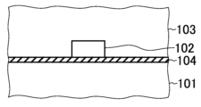
- FIG. 1 is a cross-sectional view showing a configuration of an optical device according to a first embodiment of the present invention.
- Figure 2A is a characteristic diagram showing the results of calculating the Lugiato-Lefever equation, which is commonly used in soliton comb generation simulations, using the split-step Fourier method.
- FIG. 2B is a characteristic diagram showing the spectrum of the region indicated by the double arrow in FIG. 2A and the pulse waveform in the optical resonator.
- FIG. 3 is a characteristic diagram showing the relationship between the achievable soliton step width and K c and ⁇ a / ⁇ when thermal effects are taken into consideration in the relationship between the comb light intensity and the pump light wavelength detuning shown by the solid line (a) in FIG. 2A.
- FIG. 1 is a cross-sectional view showing a configuration of an optical device according to a first embodiment of the present invention.
- Figure 2A is a characteristic diagram showing the results of calculating the Lugiato-Lefever equation, which is
- FIG. 4 is a cross-sectional view showing the configuration of another optical device according to the first embodiment of the present invention.
- Second Embodiment FIG. 5 is a cross-sectional view showing a configuration of an optical device according to a second embodiment of the present invention.
- Third Embodiment FIG. 6 is a cross-sectional view showing a configuration of an optical device according to a third embodiment of the present invention.
- FIG. 7 is a diagram for explaining the generation of a soliton comb state.
- This optical device includes a CSOI optical waveguide including an undercladding layer 101 made of an insulating material having higher heat dissipation properties than silicon oxide, and a core 102 made of a compound semiconductor.
- This optical device is an optical resonator including a CSOI optical waveguide.
- the core 102 has, for example, a so-called channel shape with a rectangular cross-sectional shape, and has a height of 400 nm and a width of 860 nm.
- an overclad layer 103 is formed on the underclad layer 101 so as to cover the core 102.
- a bonding layer 104 is formed between the underclad layer 101 and the core 102 (overclad layer 103).
- the bonding layer 104 can have a thickness of, for example, 5 nm. In this example, the bonding layer 104 is formed to cover the entire surface of the underclad layer 101.
- the core 102 is made of AlGaAs (Al composition 20%), and the undercladding layer 101 can be made of SiC, which is a material with high thermal conductivity.
- the overcladding layer 103 can be made of SiO 2 , and the bonding layer 104 can be made of SiO 2.
- Figure 2A shows the results of calculating the Lugiato-Lefever equation (LLE), which is commonly used in simulating soliton comb generation, using the split-step Fourier method.
- LLE Lugiato-Lefever equation
- Figure 2A the relationship between the comb light intensity and the pump light wavelength detuning is shown by the solid line (a).
- the pump light wavelength detuning is normalized to the optical resonator half-width, and the comb light intensity is normalized to the input pump light to the optical resonator.
- a clear soliton step is present in the region indicated by the double arrow in Figure 2A. When the spectrum of this region and the pulse waveform inside the optical resonator were checked, it was found to be a step in a single soliton state (Figure 2B).
- the parameters of the optical resonator are a ring radius of 30 ⁇ m, an internal Q value of 0.49 ⁇ 10 6 , a pump light wavelength of 1582 nm, and an input light power of 12 mW.
- the dashed line (b) shows the transition of the comb light intensity taking into account the thermal effect, calculated using K c obtained from the material structure of each layer of the above-mentioned optical device (CSOI optical waveguide).
- K c is 1.0 ⁇ 10 ⁇ 3 (W/K)
- ⁇ n/ ⁇ T is 2.2 ⁇ 10 ⁇ 4 (1/K)
- ⁇ a / ⁇ is 0.15.
- the dashed line (c) shows the transition of the comb light intensity taking into account the thermal effect in the case of a structure equivalent to the optical waveguide of Non-Patent Document 3, in which the undercladding layer is made of SiO 2.
- K c is 2.0 ⁇ 10 ⁇ 4 (W/K).
- the dashed line (b) has an intersection with the soliton step of the solid line (a), and it is clear that the soliton state can be accessed.
- the dashed line (c) does not intersect with the soliton step of the solid line (a), and it is clear that the soliton state cannot be accessed.
- a method for fabricating an optical device according to the first embodiment will be described.
- a SiC substrate is prepared, and a compound semiconductor epitaxial growth substrate having a layer structure of an AlGaAs layer/sacrificial layer/GaAs substrate is fabricated using a crystal growth apparatus such as a general MOCVD apparatus.
- a bonding layer 104 made of SiO2 is formed on the surface of the AlGaAs layer of the compound semiconductor epitaxial growth substrate by a general plasma CVD method or a sputtering method.
- the surface of the bonding layer 104 of the compound semiconductor epitaxial growth substrate and the surface of the SiC substrate are bonded by a general surface hydrophilization bonding technique.
- excellent effects such as easy bonding, improved yield, and suppression of voids can be obtained.
- the bonding layer 104 it is preferable not to use the bonding layer 104. If the bonding layer 104 is not used, the top AlGaAs layer of the growth substrate and the SiC substrate can be bonded (joined) together by a technique other than surface hydrophilization bonding, such as a surface activation bonding technique using Ar plasma irradiation.
- the GaAs substrate and sacrificial layer on the compound semiconductor epitaxial growth substrate side are removed by wet etching.
- a hard mask layer is formed of SiO2 by a general plasma CVD method or sputtering method.
- a resist pattern of an optical waveguide and a ring optical resonator is formed on the hard mask layer by electron beam drawing lithography or ultraviolet photolithography.
- the hard mask layer is patterned by dry etching using the resist pattern as a mask to form a hard mask pattern.
- the AlGaAs layer is patterned by dry etching using the hard mask pattern thus formed, forming a core 102 made of AlGaAs on the SiC substrate that will become the undercladding layer 101.
- the overcladding layer 103 is deposited by a general plasma CVD method, and the optical device structure described with reference to Figure 1 is fabricated.
- the undercladding layer 101 can be made of SiO2 , which is highly versatile (for example, a Si substrate with a thermally oxidized surface is used instead of a SiC substrate), and the overcladding layer 103 can be made of an insulating material (high thermal conductivity material) that has higher heat dissipation properties than silicon oxide such as SiC. Also, both the undercladding layer 101 and the overcladding layer 103 can be made of a high thermal conductivity material.
- the core 102 is made of AlGaAs, a III-V compound semiconductor, which provides the largest refractive index difference with the undercladding layer 101 made of SiC.
- the core can also be made of InP, InGaP, or GaP, which have lower refractive indices than AlGaAs.
- a core made of these materials provides a similarly large refractive index difference with the undercladding made of SiC.
- the band gap of the compound semiconductor that makes up the core is set so that nonlinear absorption at the pump light wavelength can be sufficiently suppressed.
- the core size in the above-described embodiment is an example, and can be adjusted as appropriate based on the design concept of the present invention.
- the core shape is not limited to the so-called channel type, but can also be the so-called rib type.
- SiC thermal conductivity 490 W/m/K
- diamond thermal conductivity 2000 W/m/K
- various materials can be applied with the intention of increasing K eff by improving the thermal conductivity according to the present invention.
- Fig. 3 shows the relationship between the accessible D range on soliton step, Kc, and ⁇ a/ ⁇ when considering thermal effects in the relationship between the comb light intensity and pump light wavelength detuning shown by the solid line (a) in Fig. 2A. It can be seen that as Kc increases, the accessible soliton step width also increases, making it easier to generate a soliton state. It can also be seen that as ⁇ a / ⁇ decreases, i.e., the absorption loss rate at the internal Q value decreases, the accessible soliton step width also increases, making it easier to generate a soliton state.
- the change in the achievable soliton step width with respect to the change in ⁇ a / ⁇ is large, but in the region where Kc is large (about 10 -1 W/K), the change in the achievable soliton step width with respect to the change in ⁇ a / ⁇ is small.
- the achievable soliton step width is not easily affected by the magnitude of the absorption loss inside the optical resonator. It is generally known that the absorption loss inside the optical resonator strongly depends on the manufacturing process, has a small degree of freedom in control, and is difficult to suppress. It is suggested that by using the structure of the optical device according to the present invention, a robust soliton comb light source can be realized against such events that are difficult to control in the manufacturing process.
- a core 102 may be disposed on an undercladding layer 101 in contact with the core 102, and an overcladding layer 103 may be formed on the undercladding layer 101.
- an overcladding layer 103 may be formed on the undercladding layer 101.
- This optical device includes a CSOI optical waveguide including an undercladding layer 121, a core 122 made of a compound semiconductor, and an overcladding layer 123 formed on the undercladding layer 121 to cover the core 122.
- This optical device is an optical resonator including a CSOI optical waveguide.
- the overcladding layer 123 is made of a material having a negative ⁇ n/ ⁇ T, which indicates the relationship between the refractive index n and the temperature T.
- the undercladding layer 121 is made of SiC, which is a material with high thermal conductivity.
- the core 122 is formed on and in contact with the undercladding layer 121.
- the cladding layer (over cladding layer 123) from a material with a negative ⁇ n/ ⁇ T, it is possible to reduce ⁇ n/ ⁇ T in the above-mentioned formula (1).
- K eff As described above, in order to realize a soliton comb state, it is important to make K eff as large as possible, and by reducing ⁇ n/ ⁇ T in formula (1), it is possible to increase K eff .
- the cladding layer by forming the cladding layer from a material with a negative ⁇ n/ ⁇ T, it is possible to reduce ⁇ n/ ⁇ T in formula (1) and increase K eff , thereby realizing soliton comb generation in a room temperature environment.
- the undercladding layer 121 from SiC, which is a material with high thermal conductivity, it is possible to increase Kc in the formula (1), and further increase Keff .
- Materials with negative ⁇ n/ ⁇ T can be, for example, titanium oxide or polymeric materials with electro-optical effects.
- Athermal optical filters have been realized that use cladding layers made of these materials and Si as a core material, which has a large ⁇ n/ ⁇ T similar to compound semiconductors, and similar configurations can be used.
- the materials with negative ⁇ n/ ⁇ T shown here are just examples, and the core size can be designed appropriately depending on the material used, taking into account the realization of anomalous dispersion, the optical confinement coefficient, the comb generation threshold, etc.
- This optical device includes a CSOI optical waveguide including an undercladding layer 131, a first core 132 made of a compound semiconductor, a second core 133 formed on the undercladding layer 131, and an overcladding layer 134 formed on the undercladding layer 131 to cover the core 132.
- This optical device is an optical resonator including a CSOI optical waveguide.
- the second core 133 is made of a material having a nonlinear optical effect in which ⁇ n/ ⁇ T, which indicates the relationship between the refractive index n and the temperature T, is lower than that of the compound semiconductor that makes up the first core 132.
- the second core 133 can be made of, for example, SiN.
- the second core 133 formed in a slab shape is formed on the undercladding layer 131, and the first core 132 is formed on the second core 133.
- the second core 133 and the first core 132 form a rib type as a whole.
- the second core 133 is not limited to a slab shape, and can be a channel type.
- the undercladding layer 131 can be made of SiC, which is a material with high thermal conductivity.
- the overcladding layer 134 can be made of SiO2 .
- the third embodiment by providing the first core 132 made of a compound semiconductor and the second core 133 made of a material having a nonlinear optical effect with a lower ⁇ n/ ⁇ T than that of the compound semiconductor, it is possible to reduce ⁇ n/ ⁇ T in the above-mentioned formula (1).
- a composite structure combining the first core 131 and the second core 133 reduces ⁇ n/ ⁇ T in formula (1) and increases K eff , thereby realizing soliton comb generation in a room temperature environment.
- the undercladding layer 131 by forming the undercladding layer 131 from SiC, which is a material with high thermal conductivity, it is possible to increase Kc in formula (1), and further increase Keff .
- the overcladding layer 133 can be formed from a material in which ⁇ n/ ⁇ T, which indicates the relationship between the refractive index n and the temperature T, is negative.
- the above-mentioned materials are just examples, and depending on the material used, the combination of the first and second cores and the core size can be appropriately designed while taking into consideration the realization of anomalous dispersion, the optical confinement factor, the comb generation threshold, etc.
- the cladding layer is made of an insulating material with higher heat dissipation properties than silicon oxide, so that soliton combs can be generated in an optical resonator using a CSOI optical waveguide at room temperature.
- the cladding layer is made of a material with a negative ⁇ n/ ⁇ T, which indicates the relationship between the refractive index n and the temperature T, so that soliton combs can be generated in an optical resonator using a CSOI optical waveguide at room temperature.
- the core has a composite structure with a first core made of a compound semiconductor and a second core made of a material with a nonlinear optical effect whose ⁇ n/ ⁇ T, which indicates the relationship between the refractive index n and the temperature T, is lower than that of a compound semiconductor, so that soliton combs can be generated in an optical resonator using a CSOI optical waveguide at room temperature.
- Keff is increased, and therefore, an excellent effect is obtained in that a soliton step region that can be realized in a room temperature environment can be obtained in an optical resonator using a CSOI optical waveguide.
- This makes it possible to generate a soliton comb in a room temperature environment with extremely low pump light intensity, which is a feature of an optical resonator using a CSOI optical waveguide, and thus makes it possible to realize a soliton comb light source on a single chip integrated with a semiconductor laser.
Landscapes
- Physics & Mathematics (AREA)
- Nonlinear Science (AREA)
- General Physics & Mathematics (AREA)
- Optics & Photonics (AREA)
- Engineering & Computer Science (AREA)
- Microelectronics & Electronic Packaging (AREA)
- Optical Modulation, Optical Deflection, Nonlinear Optics, Optical Demodulation, Optical Logic Elements (AREA)
Priority Applications (2)
| Application Number | Priority Date | Filing Date | Title |
|---|---|---|---|
| JP2024572564A JPWO2024157348A1 (https=) | 2023-01-24 | 2023-01-24 | |
| PCT/JP2023/002050 WO2024157348A1 (ja) | 2023-01-24 | 2023-01-24 | 光デバイス |
Applications Claiming Priority (1)
| Application Number | Priority Date | Filing Date | Title |
|---|---|---|---|
| PCT/JP2023/002050 WO2024157348A1 (ja) | 2023-01-24 | 2023-01-24 | 光デバイス |
Publications (1)
| Publication Number | Publication Date |
|---|---|
| WO2024157348A1 true WO2024157348A1 (ja) | 2024-08-02 |
Family
ID=91970268
Family Applications (1)
| Application Number | Title | Priority Date | Filing Date |
|---|---|---|---|
| PCT/JP2023/002050 Ceased WO2024157348A1 (ja) | 2023-01-24 | 2023-01-24 | 光デバイス |
Country Status (2)
| Country | Link |
|---|---|
| JP (1) | JPWO2024157348A1 (https=) |
| WO (1) | WO2024157348A1 (https=) |
Citations (5)
| Publication number | Priority date | Publication date | Assignee | Title |
|---|---|---|---|---|
| US20090180747A1 (en) * | 2008-01-15 | 2009-07-16 | Interuniversitair Microelektronica Centrum (Imec) | Method for Effective Refractive Index Trimming of Optical Waveguiding Structures and Optical Waveguiding Structures |
| JP2017040841A (ja) * | 2015-08-21 | 2017-02-23 | 国立大学法人 東京大学 | 光導波路素子および光集積回路装置 |
| US20180307118A1 (en) * | 2017-03-17 | 2018-10-25 | Commissariat A L'energie Atomique Et Aux Energies Alternatives | Optoelectronic device for generation a frequency comb |
| JP2019204904A (ja) * | 2018-05-24 | 2019-11-28 | 日本電信電話株式会社 | 半導体光モジュール |
| WO2023276053A1 (ja) * | 2021-06-30 | 2023-01-05 | 日本電信電話株式会社 | 光デバイス |
-
2023
- 2023-01-24 JP JP2024572564A patent/JPWO2024157348A1/ja active Pending
- 2023-01-24 WO PCT/JP2023/002050 patent/WO2024157348A1/ja not_active Ceased
Patent Citations (5)
| Publication number | Priority date | Publication date | Assignee | Title |
|---|---|---|---|---|
| US20090180747A1 (en) * | 2008-01-15 | 2009-07-16 | Interuniversitair Microelektronica Centrum (Imec) | Method for Effective Refractive Index Trimming of Optical Waveguiding Structures and Optical Waveguiding Structures |
| JP2017040841A (ja) * | 2015-08-21 | 2017-02-23 | 国立大学法人 東京大学 | 光導波路素子および光集積回路装置 |
| US20180307118A1 (en) * | 2017-03-17 | 2018-10-25 | Commissariat A L'energie Atomique Et Aux Energies Alternatives | Optoelectronic device for generation a frequency comb |
| JP2019204904A (ja) * | 2018-05-24 | 2019-11-28 | 日本電信電話株式会社 | 半導体光モジュール |
| WO2023276053A1 (ja) * | 2021-06-30 | 2023-01-05 | 日本電信電話株式会社 | 光デバイス |
Non-Patent Citations (1)
| Title |
|---|
| MA JIANBIN, WANG RUITING, LUO GUANGZHEN, MA PENGFEI, WANG PENGFEI, ZHANG YEJIN, PAN JIAOQING: "Broadened Low Anomalous Dispersion in Athermal Aluminum Nitride Hybrid Waveguides", IEEE PHOTONICS JOURNAL, IEEE, vol. 14, no. 3, 1 June 2022 (2022-06-01), pages 1 - 7, XP093195531, ISSN: 1943-0647, DOI: 10.1109/JPHOT.2022.3171435 * |
Also Published As
| Publication number | Publication date |
|---|---|
| JPWO2024157348A1 (https=) | 2024-08-02 |
Similar Documents
| Publication | Publication Date | Title |
|---|---|---|
| Chen et al. | Advances in lithium niobate photonics: development status and perspectives | |
| CN110729630B (zh) | 一种采用铌酸锂材料制成的波长高速调谐的激光器 | |
| Abel et al. | A hybrid barium titanate–silicon photonics platform for ultraefficient electro-optic tuning | |
| JP6983590B2 (ja) | 光変調器及びその製造方法 | |
| JP6622228B2 (ja) | 光変調器及びその製造方法 | |
| JP5515927B2 (ja) | 半導体光素子 | |
| US8369670B2 (en) | Optical devices having controlled nonlinearity | |
| Amarnath et al. | Electrically pumped InGaAsP-InP microring optical amplifiers and lasers with surface passivation | |
| US20230007949A1 (en) | Optical Device | |
| Grover et al. | A tunable GaInAsP-InP optical microring notch filter | |
| Liu et al. | Bandwidth and wavelength tunable all-optical filter based on cascaded opto-mechanical microring resonators | |
| Kotlyar et al. | Lithium Niobate Fabry-Perot microcavity based on strip loaded waveguides | |
| CN103688203B (zh) | 波向量匹配的谐振器及总线波导系统 | |
| Wang et al. | Design and demonstration of compact and broadband wavelength demultiplexer based on subwavelength grating (SWG) | |
| JP2018041957A (ja) | 光電変換デバイスおよび光電変換デバイスの動作波長の制御方法 | |
| Fainman et al. | Silicon nanophotonic devices for chip-scale optical communication applications | |
| WO2019198529A1 (ja) | 半導体光素子 | |
| WO2024157348A1 (ja) | 光デバイス | |
| US7034990B2 (en) | Wavelength conversion element and method for using same | |
| JP5164897B2 (ja) | 光フィルタ | |
| WO2025163879A1 (ja) | 光デバイス | |
| WO2024003979A1 (ja) | 光デバイス | |
| Tavousi et al. | Add-drop and channel-drop optical filters based on photonic crystal ring resonators | |
| CN116381852B (zh) | 一种可承受大功率光输入的铌酸锂水平端面耦合器 | |
| CN114815045A (zh) | 一种基于二维材料纳米带的多模克尔光频梳产生器件 |
Legal Events
| Date | Code | Title | Description |
|---|---|---|---|
| 121 | Ep: the epo has been informed by wipo that ep was designated in this application |
Ref document number: 23918318 Country of ref document: EP Kind code of ref document: A1 |
|
| ENP | Entry into the national phase |
Ref document number: 2024572564 Country of ref document: JP Kind code of ref document: A |
|
| WWE | Wipo information: entry into national phase |
Ref document number: 2024572564 Country of ref document: JP |
|
| NENP | Non-entry into the national phase |
Ref country code: DE |
|
| 122 | Ep: pct application non-entry in european phase |
Ref document number: 23918318 Country of ref document: EP Kind code of ref document: A1 |