WO2024154566A1 - Semiconductor device - Google Patents
Semiconductor device Download PDFInfo
- Publication number
- WO2024154566A1 WO2024154566A1 PCT/JP2023/046940 JP2023046940W WO2024154566A1 WO 2024154566 A1 WO2024154566 A1 WO 2024154566A1 JP 2023046940 W JP2023046940 W JP 2023046940W WO 2024154566 A1 WO2024154566 A1 WO 2024154566A1
- Authority
- WO
- WIPO (PCT)
- Prior art keywords
- terminal
- semiconductor device
- electrode
- resin
- lead
- Prior art date
Links
- 239000004065 semiconductor Substances 0.000 title claims abstract description 177
- 229920005989 resin Polymers 0.000 claims abstract description 231
- 239000011347 resin Substances 0.000 claims abstract description 231
- 238000007789 sealing Methods 0.000 claims abstract description 108
- 238000004891 communication Methods 0.000 claims description 6
- 230000004048 modification Effects 0.000 description 20
- 238000012986 modification Methods 0.000 description 20
- 239000000463 material Substances 0.000 description 15
- 230000017525 heat dissipation Effects 0.000 description 5
- 230000000694 effects Effects 0.000 description 4
- 239000002184 metal Substances 0.000 description 3
- 229910052751 metal Inorganic materials 0.000 description 3
- PXHVJJICTQNCMI-UHFFFAOYSA-N nickel Substances [Ni] PXHVJJICTQNCMI-UHFFFAOYSA-N 0.000 description 3
- 229910002601 GaN Inorganic materials 0.000 description 2
- JMASRVWKEDWRBT-UHFFFAOYSA-N Gallium nitride Chemical compound [Ga]#N JMASRVWKEDWRBT-UHFFFAOYSA-N 0.000 description 2
- 229910045601 alloy Inorganic materials 0.000 description 2
- 239000000956 alloy Substances 0.000 description 2
- 238000013459 approach Methods 0.000 description 2
- 239000010949 copper Substances 0.000 description 2
- 238000007747 plating Methods 0.000 description 2
- HBMJWWWQQXIZIP-UHFFFAOYSA-N silicon carbide Chemical compound [Si+]#[C-] HBMJWWWQQXIZIP-UHFFFAOYSA-N 0.000 description 2
- 229910010271 silicon carbide Inorganic materials 0.000 description 2
- 229910052709 silver Inorganic materials 0.000 description 2
- 239000004332 silver Substances 0.000 description 2
- RYGMFSIKBFXOCR-UHFFFAOYSA-N Copper Chemical compound [Cu] RYGMFSIKBFXOCR-UHFFFAOYSA-N 0.000 description 1
- BQCADISMDOOEFD-UHFFFAOYSA-N Silver Chemical compound [Ag] BQCADISMDOOEFD-UHFFFAOYSA-N 0.000 description 1
- 238000005452 bending Methods 0.000 description 1
- 239000004020 conductor Substances 0.000 description 1
- 229910052802 copper Inorganic materials 0.000 description 1
- 239000003822 epoxy resin Substances 0.000 description 1
- 230000005669 field effect Effects 0.000 description 1
- 230000006872 improvement Effects 0.000 description 1
- WABPQHHGFIMREM-AKLPVKDBSA-N lead-210 Chemical compound [210Pb] WABPQHHGFIMREM-AKLPVKDBSA-N 0.000 description 1
- 238000000034 method Methods 0.000 description 1
- 229910052759 nickel Inorganic materials 0.000 description 1
- 229920000647 polyepoxide Polymers 0.000 description 1
- 230000008569 process Effects 0.000 description 1
- 238000004080 punching Methods 0.000 description 1
- 229910052710 silicon Inorganic materials 0.000 description 1
- 239000010703 silicon Substances 0.000 description 1
- 229910000679 solder Inorganic materials 0.000 description 1
- 238000001721 transfer moulding Methods 0.000 description 1
Images


Classifications
-
- H—ELECTRICITY
- H01—ELECTRIC ELEMENTS
- H01L—SEMICONDUCTOR DEVICES NOT COVERED BY CLASS H10
- H01L23/00—Details of semiconductor or other solid state devices
- H01L23/48—Arrangements for conducting electric current to or from the solid state body in operation, e.g. leads, terminal arrangements ; Selection of materials therefor
Definitions
- This disclosure relates to a semiconductor device.
- Patent Document 1 discloses an example of a conventional semiconductor device.
- the semiconductor device disclosed in this document includes a semiconductor element, multiple leads, and sealing resin.
- the semiconductor element is mounted on a first lead, and a collector electrode on the back surface is conductive to the first lead.
- An emitter electrode on the main surface of the semiconductor element is conductive to a third lead.
- the sealing resin covers each of the multiple leads and the semiconductor element.
- the first lead has a first terminal protruding from the sealing resin
- the third lead has a third terminal protruding from the sealing resin.
- a high voltage e.g., several thousand volts
- a discharge occurs on the surface of the sealing resin between the first and third terminals, and the first and third terminals may be short-circuited.
- An object of the present disclosure is to provide a semiconductor device that is an improvement over conventional semiconductor devices.
- an object of the present disclosure is to provide a semiconductor device that can withstand a high voltage.
- the semiconductor device provided by the first aspect of the present disclosure includes a switching element having a first electrode, a second electrode, and a third electrode, and in which the first electrode and the second electrode are controlled to be turned on/off by applying a drive voltage between the third electrode and the second electrode while a potential difference is applied between the first electrode and the second electrode, a base on which the switching element is mounted, a first lead having a first terminal that is conductive with the first electrode, a second lead having a second terminal that is conductive with the second electrode, a third lead having a third terminal that is conductive with the third electrode, and a sealing resin that covers the switching element and a portion of each of the first terminal, the second terminal, and the third terminal.
- the first terminal, the second terminal, and the third terminal each include a portion that protrudes from the sealing resin to one side in a first direction perpendicular to the thickness direction of the base.
- the first terminal, the second terminal, and the third terminal are arranged spaced apart from each other in a second direction perpendicular to both the thickness direction and the first direction.
- the second terminal is located on the opposite side of the third terminal from the first terminal in the second direction.
- the above configuration allows the semiconductor device to withstand high voltages.
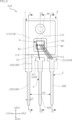
- FIG. 1 is a perspective view showing a semiconductor device according to a first embodiment of the present disclosure.
- FIG. 2 is a plan view showing the semiconductor device according to the first embodiment of the present disclosure, seen through a sealing resin.
- FIG. 3 is a bottom view showing the semiconductor device according to the first embodiment of the present disclosure.
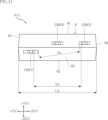
- FIG. 4 is a front view showing the semiconductor device according to the first embodiment of the present disclosure.
- FIG. 5 is a cross-sectional view taken along line VV in FIG.
- FIG. 6 is a cross-sectional view taken along line VI-VI in FIG.
- FIG. 7 is a cross-sectional view taken along line VII-VII in FIG.
- FIG. 8 is a perspective view showing a semiconductor device according to a first modification of the first embodiment.
- FIG. 9 is a bottom view showing a semiconductor device according to a first modification of the first embodiment.
- FIG. 10 is a cross-sectional view showing a semiconductor device according to a first modification of the first embodiment.
- FIG. 11 is a front view showing a semiconductor device according to a first modification of the first embodiment.
- FIG. 12 is a perspective view showing a semiconductor device according to a second modification of the first embodiment.
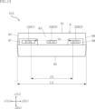
- FIG. 13 is a plan view showing a semiconductor device according to a second modification of the first embodiment.
- FIG. 14 is a front view showing a semiconductor device according to a second modification of the first embodiment.
- FIG. 15 is a perspective view showing a semiconductor device according to a third modification of the first embodiment.
- FIG. 10 is a cross-sectional view showing a semiconductor device according to a first modification of the first embodiment.
- FIG. 11 is a front view showing a semiconductor device according to a first modification of the first embodiment.
- FIG. 12 is a perspective view showing a semiconductor device according
- FIG. 16 is a plan view showing a semiconductor device according to a third modification of the first embodiment, seen through a sealing resin.
- FIG. 17 is a front view showing a semiconductor device according to a third modification of the first embodiment.
- FIG. 18 is a plan view showing a semiconductor device according to a fourth modification of the first embodiment, seen through a sealing resin.
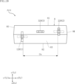
- FIG. 19 is a front view showing a semiconductor device according to a fourth modification of the first embodiment.
- FIG. 20 is a plan view showing a semiconductor device according to a second embodiment of the present disclosure.
- FIG. 21 is a plan view showing the semiconductor device according to the second embodiment of the present disclosure, seen through the sealing resin.
- FIG. 22 is a cross-sectional view taken along line XXII-XXII in FIG. FIG.
- FIG. 23 is a cross-sectional view taken along line XXIII-XXIII in FIG.
- FIG. 24 is a perspective view showing a semiconductor device according to a third embodiment of the present disclosure.
- FIG. 25 is a plan view showing a semiconductor device according to a third embodiment of the present disclosure, seen through a sealing resin.
- FIG. 26 is a front view showing a semiconductor device according to a third embodiment of the present disclosure.
- FIG. 27 is a plan view showing a semiconductor device according to a first modification of the third embodiment, seen through a sealing resin.
- FIG. 28 is a front view showing a semiconductor device according to a first modification of the third embodiment.
- an object A is formed on an object B" and “an object A is formed on an object B” include “an object A is formed directly on an object B” and “an object A is formed on an object B with another object interposed between the object A and the object B” unless otherwise specified.
- an object A is disposed on an object B” and “an object A is disposed on an object B” include “an object A is disposed directly on an object B” and “an object A is disposed on an object B with another object interposed between the object A and the object B" unless otherwise specified.
- an object A is located on an object B includes “an object A is located on an object B in contact with an object B” and “an object A is located on an object B with another object interposed between the object A and the object B” unless otherwise specified.
- an object A overlaps an object B when viewed in a certain direction includes “an object A overlaps the entire object B” and “an object A overlaps a part of an object B.”
- a surface A faces in direction B is not limited to the case where the angle of surface A with respect to direction B is 90°, but also includes the case where surface A is tilted with respect to direction B.
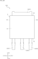
- the semiconductor device A10 includes a first lead 1, a second lead 2, a third lead 3, a switching element 6, a first conductive member 71, a second conductive member 72, and a sealing resin 8.
- FIG. 1 is a perspective view of the semiconductor device A10.
- FIG. 2 is a plan view of the semiconductor device A10, seen through the sealing resin 8.
- FIG. 3 is a bottom view of the semiconductor device A10.
- FIG. 4 is a front view of the semiconductor device A10.
- FIG. 5 is a cross-sectional view taken along line V-V in FIG. 2.
- FIG. 6 is a cross-sectional view taken along line VI-VI in FIG. 2.
- FIG. 7 is a cross-sectional view taken along line VII-VII in FIG. 2.
- the outline of the sealing resin 8 seen through is shown by an imaginary line (double-dashed line).
- the semiconductor device A10 shown in these figures is a device that is mounted on the circuit boards of various devices.
- the uses and functions of the semiconductor device A10 are not limited.
- the package format of the semiconductor device A10 is a SIP (Single Inline Package).
- the package format of the semiconductor device A10 is not limited to SIP.
- the thickness direction z corresponds to the thickness direction of the semiconductor device A10 (more specifically, for example, the sealing resin 8).
- the first direction x corresponds, for example, to the up-down direction in FIG. 2.
- the second direction y corresponds, for example, to the left-right direction in FIG. 2.
- the shape of the sealing resin 8 is rectangular. There are no particular limitations on the dimensions of the semiconductor device A10.
- the first lead 1, the second lead 2, and the third lead 3 are electrically connected to the switching element 6, and form a conductive path between the switching element 6 and the circuit wiring when the semiconductor device A10 is mounted on a circuit board.
- the first lead 1, the second lead 2, and the third lead 3 are formed, for example, by subjecting a metal plate (lead frame) to processes such as punching and bending.
- the materials constituting the first lead 1, the second lead 2, and the third lead 3 are not particularly limited, and may be, for example, either Cu (copper) or Ni (nickel), or an alloy thereof.
- the first lead 1 supports the switching element 6 and is electrically connected to the switching element 6.
- the first lead 1 has a base 110 and a first terminal 120.
- the base 110 is a portion on which the switching element 6 is mounted, and is rectangular (or approximately rectangular) when viewed in the thickness direction z.
- the base 110 has a first main surface 111, a first back surface 112, a base end surface 114, and a base through hole 113.
- the first main surface 111 and the first back surface 112 face opposite each other in the thickness direction z.
- the first main surface 111 faces the z1 side in the thickness direction z.
- the switching element 6 is bonded to the first main surface 111.
- the first back surface 112 faces the z2 side in the thickness direction z.
- the first back surface 112 is exposed from the sealing resin 8 and serves as a back surface terminal.
- the base end surface 114 is connected to the first main surface 111 and the first back surface 112, and faces the x1 side in the first direction x.
- the base through-hole 113 is a hole that extends parallel to the thickness direction z from the first main surface 111 to the first back surface 112.
- the base through-hole 113 is disposed in the center of the base 110 in the second direction y and toward the x2 side in the first direction x (toward the upper side in FIGS. 2 and 3), and is circular when viewed in the thickness direction z.
- the base through-hole 113 is separated from the switching element 6 when viewed in the thickness direction z.
- the position and shape of the base through-hole 113 are not limited.
- the first terminal 120 is connected to the base 110 and is electrically connected to the switching element 6 via the base 110.
- the first dimension L1 which is the width dimension (dimension in the second direction y) of the first terminal 120, is smaller than the width dimension (dimension in the second direction y) of the base 110.
- the plate thickness direction of the first terminal 120 coincides with the thickness direction z
- the second direction y perpendicular to both the plate thickness direction (thickness direction z) and the first direction x corresponds to the width direction of the first terminal 120.
- the first terminal 120 has a first surface 121 and a second surface 122.
- the first surface 121 and the second surface 122 are surfaces facing the plate thickness direction of the first terminal 120 and facing opposite to each other.
- the first surface 121 faces the z1 side of the thickness direction z
- the second surface 122 faces the z2 side of the thickness direction z.
- the thickness dimension (dimension in thickness direction z) of the first terminal 120 is smaller than the thickness dimension (dimension in thickness direction z) of the base 110.
- the thickness dimension of the base 110 is larger than the thickness dimension of the first terminal 120.
- the first terminal 120 is connected to the base end surface 114 of the base 110. More specifically, the first terminal 120 is connected to the base end surface 114 (and by extension the portion 110) at the end of the base end surface 114 on the y1 side in the second direction y as shown in FIG. 2, and at the end of the base end surface 114 on the z1 side in the thickness direction z as shown in FIG. 5.
- the first terminal 120 extends in the first direction x and includes a portion that protrudes from the sealing resin 8.
- the first terminal 120 includes a base end portion and a tip end portion.
- the base end portion extends from a position connected to the base 110 to a position that protrudes a short distance beyond the sealing resin 8.
- the base end portion has a larger width dimension than the tip end portion.
- the first terminal 120 includes a first straight portion 123 and a first connecting portion 124.
- the first straight portion 123 is a portion that extends straight along the first direction x, and includes a portion covered with the sealing resin 8 and a portion that protrudes from the sealing resin 8.
- the first connecting portion 124 is a portion that connects the first straight portion 123 and the base 110, and is connected to the first straight portion 123 and the base 110. As shown in FIG. 5, the first connecting portion 124 is entirely covered with the sealing resin 8 and is inclined with respect to the base 110 and the first straight portion 123.
- the first straight portion 123 has a first surface 121 (a surface facing the z1 side in the thickness direction z) that faces the same side as the first main surface 111, and is located on the z1 side in the thickness direction z with respect to the first main surface 111. Therefore, the first connecting portion 124 is inclined so that the x1 side in the first direction x is closer to the z1 side in the thickness direction z.
- the shape of the first lead 1 is not limited to the above.
- the base 110 may have a back side recess around the first back surface 112 that is recessed from the first back surface 112 to the first main surface 111 and covered by the sealing resin 8 to prevent the first lead 1 from falling out of the sealing resin 8 to the z2 side in the thickness direction z.
- the third lead 3 is electrically connected to the switching element 6.
- the third lead 3 is disposed at a distance from the first lead 1. As shown in FIG. 2, the third lead 3 is disposed on the x1 side in the first direction x of the base 110 of the first lead 1, and at the center of the base 110 in the second direction y. The third lead 3 is disposed on the y2 side in the second direction y with respect to the first terminal 120.
- the third lead 3 includes a third pad 310 and a third terminal 320.
- the third pad 310 is the portion to which the second conductive member 72 is bonded, and has a rectangular shape (or a substantially rectangular shape) that is longer in the second direction y when viewed in the thickness direction z. As shown in Figures 2 and 7, the third pad 310 has a pad main surface 311 and a pad back surface 312. The pad main surface 311 and the pad back surface 312 face opposite each other in the thickness direction z. The pad main surface 311 faces the z1 side in the thickness direction z. An end of the second conductive member 72 is bonded to the pad main surface 311. The pad back surface 312 faces the z2 side in the thickness direction z.
- the third pad 310 is entirely covered with sealing resin 8.
- the third terminal 320 is connected to the third pad 310 and is electrically connected to the switching element 6 via the third pad 310 and the second conductive member 72.
- the width dimension (dimension in the second direction y) of the third terminal 320 is smaller than the width dimension (dimension in the second direction y) of the third pad 310.
- the thickness dimension (dimension in the thickness direction z) of the third terminal 320 is the same as the thickness dimension (dimension in the thickness direction z) of the third pad 310 and is the same as the thickness dimension of the first terminal 120.
- the third terminal 320 is disposed on the x1 side of the third pad 310 in the first direction x and in the center in the second direction y.
- the third terminal 320 is located on the y2 side of the first terminal 120 in the second direction y.
- the third terminal 320 has a fifth surface 321 and a sixth surface 322.
- the fifth surface 321 and the sixth surface 322 are surfaces that face in the plate thickness direction of the third terminal 320 and face in opposite directions to each other. As shown in FIG. 7, the fifth surface 321 faces the z1 side in the thickness direction z, and the sixth surface 322 faces the z2 side in the thickness direction z.
- the third terminal 320 extends in the first direction x and includes a portion that protrudes from the sealing resin 8.
- the third terminal 320 has a width dimension larger than that of the tip side portion from the position connected to the third pad 310 to a position protruding a short distance beyond the sealing resin 8.
- the shape of the third lead 3 is not limited to the above.
- the second lead 2 is electrically connected to the switching element 6.
- the second lead 2 is disposed at a distance from the first lead 1 and the second lead 2.
- the second lead 2 is disposed on the x1 side in the first direction x of the base 110 of the first lead 1, at a position corresponding to the end of the first terminal 120 on the y2 side in the second direction y in the second direction y.
- the second lead 2 and the third lead 3 are located at the same position in the thickness direction z.
- the second lead 2 includes a second pad 210 and a second terminal 220.
- the second pad 210 is the portion to which the first conductive member 71 is bonded, and has a rectangular shape (or a substantially rectangular shape) that is long in the second direction y when viewed in the thickness direction z. As shown in Figures 2 and 6, the second pad 210 has a pad main surface 211 and a pad back surface 212. The pad main surface 211 and the pad back surface 212 face opposite each other in the thickness direction z. The pad main surface 211 faces the z1 side in the thickness direction z. An end of the first conductive member 71 is bonded to the pad main surface 211. The pad back surface 212 faces the z2 side in the thickness direction z. The second pad 210 is entirely covered with sealing resin 8.
- the second terminal 220 is connected to the second pad 210 and is electrically connected to the switching element 6 via the second pad 210 and the first conductive member 71.
- the width dimension (dimension in the second direction y) of the second terminal 220 is smaller than the width dimension (dimension in the second direction y) of the second pad 210.
- the thickness dimension (dimension in the thickness direction z) of the second terminal 220 is the same as the thickness dimension (dimension in the thickness direction z) of the second pad 210 and is the same as the thickness dimension of the first terminal 120.
- the second terminal 220 is disposed on the x1 side of the first direction x and in the center of the second direction y with respect to the second pad 210.
- the second terminal 220 is located on the y2 side of the second direction y with respect to the third terminal 320 in the second direction y.
- the second terminal 220 is located on the opposite side of the first terminal 120 with respect to the third terminal 320 in the second direction y.
- the second terminal 220 has a third surface 221 and a fourth surface 222.
- the third surface 221 and the fourth surface 222 are surfaces that face the plate thickness direction of the second terminal 220 and face opposite each other. As shown in FIG. 6, the third surface 221 faces the z1 side in the thickness direction z, and the fourth surface 222 faces the z2 side in the thickness direction z.
- the second terminal 220 extends in the first direction x and includes a portion that protrudes from the sealing resin 8.
- the second terminal 220 has a width dimension larger than that of the tip side portion from the position connected to the second pad 210 to a position protruding a short distance beyond the sealing resin 8.
- the shape of the second lead 2 is not limited to the above.
- the portions of the first terminal 120, the second terminal 220, and the third terminal 320 exposed from the sealing resin 8 have the same shape.
- the tip of the first terminal 120 (the end on the x1 side in the first direction x opposite the portion connected to the base 110), the tip of the second terminal 220 (the end on the x1 side in the first direction x opposite the portion connected to the second pad 210), and the tip of the third terminal 320 (the end on the x1 side in the first direction x opposite the portion connected to the third pad 310) are in the same position in the first direction x.
- the second terminal 220 is located on the opposite side of the third terminal 320 from the first terminal 120 in the second direction y.
- the first distance D1 which is the distance between the first terminal 120 and the second terminal 220 in the second direction y, is larger than the width dimension (first dimension L1) of the first terminal 120.
- the distance (first distance D1) between the first terminal 120 and the second terminal 220 in the second direction y is 3 to 11 times the width dimension (first dimension L1) of the first terminal 120.
- An outer plating layer made of, for example, an alloy mainly composed of Sn may be formed on the portions of the first lead 1, the second lead 2, and the third lead 3 exposed from the sealing resin 8.
- An inner plating layer made of, for example, Ag may be formed on the region of the first main surface 111 of the first lead 1 to which the switching element 6 is bonded, the region of the pad main surface 211 of the second lead 2 to which the first conductive member 71 is bonded, and the region of the pad main surface 311 of the third lead 3 to which the second conductive member 72 is bonded.
- the switching element 6 is an element that realizes the switching function to be performed by the semiconductor device A10. There is no particular limitation on the type of the switching element 6.
- the switching element 6 is a transistor such as a metal-oxide-semiconductor field-effect transistor (MOSFET).
- MOSFET metal-oxide-semiconductor field-effect transistor
- the switching element 6 includes an element body 60, a first electrode 63, a second electrode 64, and a third electrode 65.
- the element body 60 is plate-shaped and rectangular when viewed in the thickness direction z.
- the element body 60 is made of a semiconductor material, and in this embodiment, is made of Si (silicon).
- the material of the element body 60 is not limited, and may be other materials such as SiC (silicon carbide) and GaN (gallium nitride).
- the element body 60 has an element main surface 61 and an element back surface 62.
- the element main surface 61 and the element back surface 62 face opposite each other in the thickness direction z.
- the element main surface 61 faces the z1 side in the thickness direction z.
- the element back surface 62 faces the z2 side in the thickness direction z.
- the second electrode 64 and the third electrode 65 are arranged on the element main surface 61.
- the first electrode 63 is arranged on the element back surface 62.
- the first electrode 63 is a drain electrode
- the second electrode 64 is a source electrode
- the third electrode 65 is a gate electrode.
- the second electrode 64 is larger than the third electrode 65.
- the switching element 6 applies a driving voltage to the third electrode 65 (gate electrode) and the second electrode 64 (source electrode) while applying a potential difference between the first electrode 63 (drain electrode) and the second electrode 64 (source electrode), thereby controlling the on/off of the first electrode 63 (drain electrode) and the second electrode 64 (source electrode).
- the switching element 6 is mounted at the center of the first main surface 111 in the second direction y, toward the x1 side in the first direction x.
- the switching element 6 is disposed at a position that does not overlap the base through-hole 113 when viewed in the thickness direction z.
- the switching element 6 is bonded to the first main surface 111 via a bonding material 69, with the element back surface 62 facing the first main surface 111.
- the bonding material 69 is a conductive bonding material, such as solder.
- the bonding material 69 may be other conductive bonding materials such as silver paste and sintered silver bonding material.
- the first electrode 63 of the switching element 6 is bonded to the first main surface 111 by the bonding material 69, and is electrically connected to the first lead 1.
- the first conductive member 71 is joined to the second electrode 64 of the switching element 6 and the pad main surface 211 of the second lead 2.
- the second electrode 64 of the switching element 6 is electrically connected to the second lead 2.
- the second conductive member 72 is joined to the third electrode 65 of the switching element 6 and the pad main surface 311 of the third lead 3.
- the third electrode 65 of the switching element 6 is electrically connected to the third lead 3.
- the first conductive member 71 and the second conductive member 72 are, for example, wires (bonding wires).
- the material, thickness, and number of the first conductive member 71 and the second conductive member 72 are not limited. In the illustrated example, multiple (three) first conductive members 71 are joined to the second electrode 64 and the pad main surface 211.
- the first conductive member 71 connecting the switching element 6 and the second lead 2, and the second conductive member 72 connecting the switching element 6 and the third lead 3 may be made of a conductive material other than a wire (such as a metal plate or a metal ribbon).
- a high voltage is applied from the outside between the first terminal 120 (drain terminal) and the second terminal 220 (source terminal).
- the potential difference between the first terminal 120 (drain terminal) and the third terminal 320 (gate terminal) also increases according to the applied high voltage.
- the sealing resin 8 covers parts of the first lead 1, the second lead 2, and the third lead 3, as well as the switching element 6, the first conductive member 71, and the second conductive member 72.
- the sealing resin 8 is made of, for example, a black epoxy resin. There are no limitations on the material of the sealing resin 8.
- the sealing resin 8 is formed, for example, by transfer molding using a mold.
- the sealing resin 8 has a resin main surface 81, a resin back surface 82, a resin end surface 83, a first resin side surface 84, a second resin side surface 85, and a third resin side surface 86.
- the resin main surface 81 and the resin back surface 82 face opposite each other in the thickness direction z.
- the resin main surface 81 faces the z1 side in the thickness direction z
- the resin back surface 82 faces the z2 side in the thickness direction z.
- the first back surface 112 of the first lead 1 is exposed from the resin back surface 82 over its entirety, and the resin back surface 82 and the first back surface 112 are flush with each other.
- the resin end surface 83 and the first resin side surface 84 are surfaces connected to the resin main surface 81 and the resin back surface 82, respectively.
- the resin end surface 83 and the first resin side surface 84 face opposite each other in the first direction x.
- the resin end surface 83 is a surface located on the x1 side of the first direction x and facing the x1 side of the first direction x.
- the first resin side surface 84 is a surface located on the x2 side of the first direction x and facing the x2 side of the first direction x.
- the second resin side surface 85 and the third resin side surface 86 are surfaces connected to the resin main surface 81, the resin back surface 82, the resin end surface 83, and the first resin side surface 84, respectively.
- the second resin side surface 85 and the third resin side surface 86 face opposite each other in the second direction y.
- the second resin side surface 85 is a surface located on the y1 side of the second direction y and facing the y1 side of the second direction y.
- the third resin side surface 86 is a surface that is disposed on the y2 side in the second direction y and faces the y2 side in the second direction y.
- the resin end surface 83, the first resin side surface 84, the second resin side surface 85, and the third resin side surface 86 each have a surface that is connected to the resin main surface 81 and inclined so as to approach each other toward the resin main surface 81.
- the sealing resin 8 has a tapered shape in which the cross-sectional area in the xy plane of the sealing resin 8 is smaller toward the resin main surface 81.
- the resin end surface 83, the first resin side surface 84, the second resin side surface 85, and the third resin side surface 86 each have a surface that is connected to the resin back surface 82 and inclined so as to approach each other toward the resin back surface 82.
- the sealing resin 8 has a tapered shape in which the cross-sectional area in the xy plane of the sealing resin 8 is smaller toward the resin back surface 82.
- the shapes of the resin end surface 83, the first resin side surface 84, the second resin side surface 85, and the third resin side surface 86 are not limited.
- the resin end surface 83 is a surface facing the direction in which the first terminal 120, the second terminal 220, and the third terminal 320 protrude.
- the first terminal 120, the second terminal 220, and the third terminal 320 protrude from the resin end surface 83.
- the first terminal 120, the third terminal 320, and the second terminal 220 are spaced apart from each other in the second direction y, and are arranged in this order from the y1 side of the second direction y to the y2 side of the second direction y.
- the second terminal 220 is located on the opposite side of the third terminal 320 from the first terminal 120 in the second direction y.
- the ratio of the distance (first distance D1) between the first terminal 120 and the second terminal 220 in the second direction y to the dimension (second dimension L2) between the second resin side surface 85 and the third resin side surface 86 of the sealing resin 8 in the second direction y is large.
- the ratio of the distance (first distance D1) between the first terminal 120 and the second terminal 220 in the second direction y to the dimension (second dimension L2) between the second resin side surface 85 and the third resin side surface 86 of the sealing resin 8 in the second direction y is 20% to 85%.
- the first terminal 120, the second terminal 220, and the third terminal 320 are disposed at the same position in the thickness direction z on the resin end surface 83.
- the sealing resin 8 has a resin through hole 89.
- the resin through hole 89 is a through hole that extends parallel to the thickness direction z from the resin main surface 81 to the resin back surface 82.
- the resin through hole 89 is disposed at the center of the sealing resin 8 in the second direction y and toward the x2 side in the first direction x (toward the upper side in FIG. 2), and is circular when viewed in the thickness direction z.
- the center of the resin through hole 89 is the same as the center of the base through hole 113.
- the diameter of the resin through hole 89 is smaller than the diameter of the base through hole 113. As shown in FIGS.
- the resin through hole 89 is located inside the base through hole 113, and the hole wall of the resin through hole 89 is entirely formed by the sealing resin 8.
- the base 110 is not exposed from the hole wall of the resin through hole 89.
- the resin through hole 89 is used, for example, to attach a heat dissipation member to the semiconductor device A10 by inserting a fastening member such as a screw through the resin through hole 89.
- the first back surface 112 is connected to the heat dissipation member via an electrical insulating sheet or the like, so that heat generated by the switching element 6 is dissipated via the base 110 and the heat dissipation member.
- the first lead 1 has a first terminal 120
- the second lead 2 has a second terminal 220
- the third lead 3 has a third terminal 320.
- the first terminal 120, the second terminal 220, and the third terminal 320 each protrude from the resin end surface 83 (sealing resin 8) toward the x1 side of the first direction x.
- the first terminal 120, the second terminal 220, and the third terminal 320 are arranged spaced apart from each other in the second direction y.
- the second terminal 220 is located on the opposite side of the first terminal 120 with respect to the third terminal 320 in the second direction y. This terminal arrangement allows the distance (first distance D1) between the first terminal 120 and the second terminal 220 in the second direction y to be increased.
- the distance (first distance D1) between the first terminal 120 and the second terminal 220 in the second direction y is 3 to 11 times the dimension (first dimension L1) in the width direction of the first terminal 120.
- the ratio of the distance (first distance D1) between the first terminal 120 and the second terminal 220 in the second direction y to the dimension (second dimension L2) between the second resin side surface 85 and the third resin side surface 86 of the sealing resin 8 in the second direction y is 20% to 85%.
- the creepage distance Dc which is the shortest distance connecting the location where the first terminal 120 protrudes from the sealing resin 8 and the location where the second terminal 220 protrudes from the sealing resin 8 along the surface of the sealing resin 8, can be secured sufficiently large compared to the case where the first terminal 120 and the second terminal 220 are arranged at positions adjacent to each other in the second direction y.
- the semiconductor device A10 can suppress discharge at the resin end surface 83 even when a high voltage is applied between the first terminal 120 and the second terminal 220. Therefore, the semiconductor device A10 of this embodiment can achieve high voltage resistance.
- the pad back surface 212 is exposed from the resin back surface 82.
- the semiconductor device A10 can dissipate heat emitted by the switching element 6 by connecting a heat dissipation member to the pad back surface 212.
- the sealing resin 8 has a resin through hole 89 extending parallel to the thickness direction z.
- the semiconductor device A10 can easily attach a heat dissipation member by inserting a fastening member such as a screw through the resin through hole 89.
- the center of the resin through hole 89 is the same as the center of the base through hole 113, and the diameter of the resin through hole 89 is smaller than the diameter of the base through hole 113.
- the resin through hole 89 is located inside the base through hole 113, and the hole wall of the resin through hole 89 is entirely formed by the sealing resin 8.
- the base 110 is not exposed from the hole wall of the resin through hole 89. This insulates the base 110 from the fastening member.
- the thickness dimension of the base 110 is greater than the thickness dimensions of the first terminal 120, the second lead 2, and the third lead 3.
- the semiconductor device A10 can efficiently absorb the heat emitted by the switching element 6 into the base 110.
- the base 110 has a base through hole 113 and the sealing resin 8 has a resin through hole 89 has been described, but the present disclosure is not limited to this.
- the base 110 does not have to have a base through hole 113, and the sealing resin 8 does not have to have a resin through hole 89. This also applies to the other embodiments and modified examples described below.
- FIGS. 8 to 19 show modified examples of the semiconductor device A10 according to the first embodiment.
- elements that are the same as or similar to those in the above embodiment are given the same reference numerals as in the above embodiment, and duplicated descriptions will be omitted.
- Figures 8 to 11 show a semiconductor device A11 according to a first modified example of the first embodiment.
- Figure 8 is a perspective view of the semiconductor device A11.
- Figure 9 is a bottom view of the semiconductor device A11, which corresponds to Figure 3.
- Figure 10 is a cross-sectional view of the semiconductor device A11, which corresponds to Figure 5.
- Figure 11 is a front view of the semiconductor device A11.
- the semiconductor device A11 differs from the semiconductor device A10 of the above embodiment in the configuration of the first lead 1.
- the first terminal 120 extends entirely straight along the first direction x.
- the position at which the first terminal 120 protrudes from the resin end surface 83 is on the z2 side in the thickness direction z compared to the semiconductor device A10.
- the position of the first terminal 120 in the thickness direction z is different from the positions of the second terminal 220 and the third terminal 320 in the thickness direction z.
- the first terminal 120 and the second terminal 220 and the third terminal 320 are spaced apart from each other in the thickness direction z.
- the first back surface 112 of the base 110 is not exposed from the resin back surface 82 and is covered by the sealing resin 8.
- the position at which the first terminal 120 protrudes from the resin end surface 83 is on the z2 side in the thickness direction z from the position at which the second terminal 220 protrudes from the resin end surface 83.
- the creepage distance Dc between the first terminal 120 and the second terminal 220 on the surface of the sealing resin 8 can be extended more than in the semiconductor device A10. This makes it possible to increase the voltage resistance of the semiconductor device A11.
- FIG. 12 is a perspective view of the semiconductor device A12.
- Fig. 13 is a plan view of the semiconductor device A12.
- Fig. 14 is a front view of the semiconductor device A12.
- the semiconductor device A12 differs from the semiconductor device A10 of the above embodiment in the configuration of the sealing resin 8.
- the sealing resin 8 has a first convex portion 87 and a second convex portion 88.
- the first convex portion 87 and the second convex portion 88 each protrude from the resin end surface 83 toward the x1 side in the first direction x.
- the first convex portion 87 is provided at a position corresponding to the first terminal 120, and the first terminal 120 protrudes from the first convex portion 87.
- the second convex portion 88 is provided at a position corresponding to the second terminal 220, and the second terminal 220 protrudes from the second convex portion 88.
- the creepage distance Dc between the first terminal 120 and the second terminal 220 on the surface of the sealing resin 8 can be extended more than in the semiconductor device A10. This makes it possible to increase the withstand voltage of the semiconductor device A12.
- FIG. 15 to 17 show a semiconductor device A13 according to a third modified example of the first embodiment.
- Fig. 15 is a perspective view of the semiconductor device A13.
- Fig. 16 is a plan view of the semiconductor device A13, and corresponds to Fig. 2.
- the outline of the sealing resin 8 is shown by an imaginary line (two-dot chain line) through the sealing resin 8.
- Fig. 17 is a front view of the semiconductor device A13.
- the semiconductor device A13 differs from the semiconductor device A11 of the above modification mainly in the configuration of the first terminal 120 in the first lead 1.
- the first terminal 120 has a first twisted portion 125.
- the first twisted portion 125 is a portion of the first terminal 120 that is twisted 90° around the first direction x, which is the longitudinal direction of the first terminal 120, at a portion of the first terminal 120 covered with the sealing resin 8.
- the first terminal 120 has the first twisted portion 125, so that the first surface 121 and the second surface 122 face both sides of the second direction y at the portion of the first terminal 120 exposed from the sealing resin 8.
- the first terminal 120 without the first twisted portion 125 is shown by an imaginary line (two-dot chain line).
- the creepage distance Dc between the first terminal 120 and the second terminal 220 on the surface of the sealing resin 8 can be extended more than in the semiconductor device A10 and the semiconductor device A11. This makes it possible to increase the withstand voltage of the semiconductor device A13.
- Figures 18 and 19 show a semiconductor device A14 according to a fourth modification of the first embodiment.
- Figure 18 is a plan view of the semiconductor device A14, and corresponds to Figure 2.
- the outline of the sealing resin 8 is shown by an imaginary line (two-dot chain line) through the sealing resin 8.
- Figure 19 is a front view of the semiconductor device A14.
- the semiconductor device A14 differs from the semiconductor device A13 of the above modified example in the configuration of the second terminal 220 in the second lead 2.
- the second terminal 220 in addition to the first terminal 120 having the first twisted portion 125, the second terminal 220 has a second twisted portion 223.
- the second twisted portion 223 is a portion of the second terminal 220 that is twisted 90 degrees around the first direction x, which is the longitudinal direction of the second terminal 220, in a portion of the second terminal 220 that is covered with the sealing resin 8.
- the second terminal 220 since the second terminal 220 has the second twisted portion 223, the third surface 221 and the fourth surface 222 face on both sides of the second direction y in the portion of the second terminal 220 that is exposed from the sealing resin 8.
- the first terminal 120 when the first terminal 120 does not have the first twisted portion 125 and the second terminal 220 when the second terminal 220 does not have the second twisted portion 223 are shown by imaginary lines (double-dashed lines).
- the creepage distance Dc between the first terminal 120 and the second terminal 220 on the surface of the sealing resin 8 can be extended more than in the semiconductor device A13. This makes it possible to increase the withstand voltage of the semiconductor device A14.
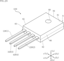
- FIGS. 20 to 26 show other embodiments of the present disclosure.
- elements that are the same as or similar to those in the above embodiment are given the same reference numerals as in the above embodiment, and duplicated descriptions are omitted.
- FIG. 20 to 23 show a semiconductor device A20 according to a second embodiment of the present disclosure.
- FIG. 20 is a plan view of the semiconductor device A20.
- FIG. 21 is a plan view of the semiconductor device A20, seen through the sealing resin 8. In FIG. 21, for ease of understanding, the outline of the see-through sealing resin 8 is shown by an imaginary line (two-dot chain line).
- FIG. 22 is a cross-sectional view taken along line XXII-XXII in FIG. 21.
- FIG. 23 is a cross-sectional view taken along line XXIII-XXIII in FIG. 21.
- the semiconductor device A20 of this embodiment has a surface mount type package structure.
- the first lead 1 has a base 110, a first terminal 120, and an extension 130.
- the extension 130 is connected to the base 110.
- the extension 130 is located on the opposite side of the base 110 from the first terminal 120 in the first direction x.
- the extension 130 extends from the base 110 to the x2 side in the first direction x, and protrudes from the first resin side surface 84 of the sealing resin 8 to the x2 side in the first direction x.
- the first terminal 120, the second terminal 220, and the third terminal 320 each have a bent portion exposed from the sealing resin 8.
- the tip portion on the x1 side in the first direction x is located on the z2 side in the thickness direction z of the portion protruding from the sealing resin 8 (resin end surface 83).
- the first terminal 120, the second terminal 220, and the third terminal 320 each protrude from the resin end surface 83 (sealing resin 8) toward the x1 side in the first direction x.
- the second terminal 220 is located on the opposite side of the first terminal 120 with respect to the third terminal 320 in the second direction y.
- This terminal arrangement allows the distance (first distance D1) between the first terminal 120 and the second terminal 220 in the second direction y to be increased.
- the creepage distance between the first terminal 120 and the second terminal 220 on the surface of the sealing resin 8 can be secured sufficiently large compared to the case where the first terminal 120 and the second terminal 220 are located adjacent to each other in the second direction y.
- the semiconductor device A20 has a common configuration with the semiconductor device A10, and thus achieves the same effects as the semiconductor device A10.
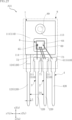
- FIG. 24 is a perspective view of the semiconductor device A30.
- Fig. 25 is a plan view of the semiconductor device A30, and corresponds to Fig. 2.
- the outline of the sealing resin 8 is shown by an imaginary line (two-dot chain line) through the sealing resin 8.
- Fig. 26 is a front view of the semiconductor device A30.
- the semiconductor device A30 of this embodiment further includes a fourth lead 4 and a third conductive member 73.
- the fourth lead 4 is electrically connected to the switching element 6. As shown in FIG. 25, the fourth lead 4 is disposed apart from the first lead 1, the second lead 2, and the third lead 3. The fourth lead 4 is disposed on the x1 side of the base 110 of the first lead 1 in the first direction x, between the second lead 2 and the third lead 3 in the second direction y. As shown in FIG. 26, in this embodiment, the position of the fourth lead 4 in the thickness direction z is the same as that of the second lead 2 and the third lead 3.
- the fourth lead 4 includes a fourth pad 410 and a fourth terminal 420.
- the fourth pad 410 is the portion to which the third conductive member 73 is bonded, and has a rectangular shape (or a roughly rectangular shape) that is longer in the second direction y when viewed in the thickness direction z.
- the fourth pad 410 has a pad main surface 411.
- the pad main surface 411 faces the z1 side in the thickness direction z, and the third conductive member 73 is bonded to it.
- the third conductive member 73 is a wire (bonding wire). There are no limitations on the material, thickness, or number of the third conductive member 73.
- the fourth pad 410 is entirely covered with sealing resin 8.
- the fourth terminal 420 is connected to the fourth pad 410 and is electrically connected to the second electrode 64 (source electrode) of the switching element 6 via the fourth pad 410 and the third conductive member 73.
- the fourth terminal 420 functions as a source sense terminal of the semiconductor device A30.
- the width dimension (dimension in the second direction y) of the fourth terminal 420 is smaller than the width dimension (dimension in the second direction y) of the fourth pad 410.
- the thickness dimension (dimension in the thickness direction z) of the fourth terminal 420 is the same as the thickness dimension (dimension in the thickness direction z) of the fourth pad 410 and is the same as the thickness dimension of the first terminal 120. As shown in FIG.
- the fourth terminal 420 is disposed on the x1 side of the first direction x and in the center in the second direction y with respect to the fourth pad 410.
- the fourth terminal 420 extends in the first direction x and includes a portion protruding from the sealing resin 8.
- the shape of the fourth lead 4 is not limited to the above.
- the first terminal 120, the third terminal 320, the fourth terminal 420, and the second terminal 220 are spaced apart from one another in the second direction y on the resin end surface 83, and are arranged in this order from the y1 side of the second direction y to the y2 side of the second direction y.
- the first terminal 120 and the second terminal 220 are located on the outermost sides opposite one another in the second direction y among the first terminal 120, the second terminal 220, the third terminal 320, and the fourth terminal 420.
- the first terminal 120, the second terminal 220, the third terminal 320, and the fourth terminal 420 are arranged at the same position in the thickness direction z on the resin end surface 83.
- the second terminal 220 is located on the opposite side of the third terminal 320 from the first terminal 120 in the second direction y.
- the first terminal 120 and the second terminal 220 are located on the outermost sides of the first terminal 120 to the fourth terminal 420 on the opposite sides in the second direction y.
- This terminal arrangement makes it possible to increase the distance (first distance D1) between the first terminal 120 and the second terminal 220 in the second direction y.
- the semiconductor device A30 to have a high withstand voltage.
- the semiconductor device A30 has a common configuration with the semiconductor device A10 and thus achieves the same effects as the semiconductor device A10.
- FIGS. 27 and 28 show a modified example of the semiconductor device A30 according to the third embodiment.
- elements that are the same as or similar to those in the third embodiment above are given the same reference numerals as in the above embodiment, and duplicated descriptions are omitted.
- Figures 27 and 28 show a semiconductor device A31 according to a first modified example of the third embodiment.
- Figure 27 is a plan view of the semiconductor device A31, and corresponds to Figure 2.
- the outline of the sealing resin 8 is shown by an imaginary line (two-dot chain line) through the sealing resin 8.
- Figure 28 is a front view of the semiconductor device A31.
- the semiconductor device A31 differs from the semiconductor device A30 of the above embodiment mainly in the arrangement of the second lead 2 and the fourth lead 4.
- the arrangement of the second lead 2 and the fourth lead 4 is swapped compared to the semiconductor device A30.
- the fourth lead 4 is arranged on the y2 side of the second direction y relative to the second lead 2 in the second direction y.
- the first terminal 120, the third terminal 320, the second terminal 220, and the fourth terminal 420 are spaced apart from each other in the second direction y on the resin end surface 83, and are arranged in this order from the y1 side of the second direction y to the y2 side of the second direction y.
- the second terminal 220 is located on the opposite side of the third terminal 320 from the first terminal 120 in the second direction y.
- This arrangement of terminals allows the distance (first distance D1) between the first terminal 120 and the second terminal 220 in the second direction y to be increased.
- the semiconductor device A31 has a configuration in common with the semiconductor device A10, and thus provides the same effects as the semiconductor device A10.
- the semiconductor device according to the present disclosure is not limited to the above-mentioned embodiment.
- the specific configuration of each part of the semiconductor device according to the present disclosure can be freely designed in various ways.
- Appendix 1 a switching element having a first electrode, a second electrode, and a third electrode, the first electrode and the second electrode being on/off controlled by applying a drive voltage between the third electrode and the second electrode while a potential difference is applied between the first electrode and the second electrode; a first lead having a base on which the switching element is mounted and a first terminal electrically connected to the first electrode; a second lead having a second terminal in electrical communication with the second electrode; a third lead having a third terminal in electrical communication with the third electrode; a sealing resin that covers the switching element, and a portion of each of the first terminal, the second terminal, and the third terminal; the first terminal, the second terminal, and the third terminal each include a portion protruding from the sealing resin to one side in a first direction perpendicular to a thickness direction of the base, the first terminal, the second terminal, and the third terminal are disposed apart from one another in the thickness direction and in a second direction perpendicular to the
- the first terminal has a first surface and a second surface facing in opposite directions and is plate-shaped extending in the first direction; 2.
- the semiconductor device according to claim 1 wherein the second terminal has a third surface and a fourth surface facing opposite each other and is plate-shaped extending in the first direction.
- Appendix 3. 3.
- Appendix 4. 4.
- the sealing resin has a resin main surface and a resin back surface facing opposite each other in the thickness direction, a resin end surface connected to the resin main surface and the resin back surface and facing one side in the first direction, a first resin side surface facing the other side in the first direction, and a second resin side surface and a third resin side surface facing opposite each other in the second direction.
- Appendix 8 The semiconductor device described in Appendix 7, wherein when a dimension in a second direction between the second resin side surface and the third resin side surface is a second dimension, and a distance in the second direction between the first terminal and the second terminal is a first distance, a ratio of the first distance to the second dimension is 20% to 85%.
- the sealing resin has a first protrusion protruding from the resin end surface to one side in the first direction, 9. The semiconductor device according to claim 7, wherein the first terminal protrudes from the first protrusion.
- Appendix 10. the sealing resin has a second protrusion protruding from the resin end surface to one side in the first direction, 10. The semiconductor device according to claim 7, wherein the second terminal protrudes from the second protrusion.
- Appendix 11. a first conductive member conductively connected to the second electrode and the second lead; a second conductive member conductively connected to the third electrode and the third lead, 11.
- the semiconductor device according to claim 1 wherein the first conductive member and the second conductive member are covered with the sealing resin.
- the second lead includes a first pad connected to the second terminal on the other side in the first direction and to which the first conductive member is conductively joined; 12.
- the third lead is connected to the other side of the third terminal in the first direction and has a second pad to which the second conductive member is conductively joined.
- the switching element has a main surface facing one side in the thickness direction and a back surface facing the other side in the thickness direction, the first electrode is a drain electrode and is disposed on a rear surface of the element; the second electrode is a source electrode and is disposed on the main surface of the element; the third electrode is a gate electrode and is disposed on the main surface of the element; the first electrode is conductively bonded to the base; 13.
- the semiconductor device wherein the first terminal is connected to the base.
- Appendix 14. a fourth lead having a fourth terminal in electrical communication with the second electrode; 14.
- Appendix 15. 15. The semiconductor device according to claim 14, wherein the first terminal and the second terminal are located at outermost positions opposite to each other in the second direction among the first terminal to the fourth terminal.
Landscapes
- Physics & Mathematics (AREA)
- Condensed Matter Physics & Semiconductors (AREA)
- General Physics & Mathematics (AREA)
- Engineering & Computer Science (AREA)
- Computer Hardware Design (AREA)
- Microelectronics & Electronic Packaging (AREA)
- Power Engineering (AREA)
- Structures Or Materials For Encapsulating Or Coating Semiconductor Devices Or Solid State Devices (AREA)
Abstract
This semiconductor device comprises: a switching element in which a part between a first electrode and a second electrode is controlled on/off by applying a drive voltage between a third electrode and the second electrode in a state where a potential difference is set between the first electrode and the second electrode; a first terminal conductive to the first electrode; a second terminal conductive to the second electrode; a third terminal conductive to the third electrode; and a sealing resin. The first terminal, the second terminal, and the third terminal each include portions projected from the sealing resin. The first terminal, the second terminal, and the third terminal are spaced apart from each other in a second direction. The second terminal is positioned opposite to the first terminal relative to the third terminal in the second direction.
Description
本開示は、半導体装置に関する。
This disclosure relates to a semiconductor device.
半導体素子を備えた半導体装置は、様々な構成が提案されている。特許文献1には、従来の半導体装置の一例が開示されている。同文献に開示された半導体装置は、半導体素子、複数のリードおよび封止樹脂を備えている。半導体素子は、第1リードに搭載され、裏面のコレクタ電極が第1リードに導通している。半導体素子の主面のエミッタ電極が第3リードに導通している。封止樹脂は、複数のリードの一部ずつと半導体素子とを覆っている。第1リードは封止樹脂から突出する第1端子を備え、第3リードは封止樹脂から突出する第3端子を備えている。当該半導体装置の第1端子と第3端子との間に高電圧(たとえば数千V)が印加されると、第1端子と第3端子との間の封止樹脂の表面上で放電が起こり、第1端子と第3端子とが短絡する場合がある。
Various configurations have been proposed for semiconductor devices equipped with semiconductor elements. Patent Document 1 discloses an example of a conventional semiconductor device. The semiconductor device disclosed in this document includes a semiconductor element, multiple leads, and sealing resin. The semiconductor element is mounted on a first lead, and a collector electrode on the back surface is conductive to the first lead. An emitter electrode on the main surface of the semiconductor element is conductive to a third lead. The sealing resin covers each of the multiple leads and the semiconductor element. The first lead has a first terminal protruding from the sealing resin, and the third lead has a third terminal protruding from the sealing resin. When a high voltage (e.g., several thousand volts) is applied between the first and third terminals of the semiconductor device, a discharge occurs on the surface of the sealing resin between the first and third terminals, and the first and third terminals may be short-circuited.
本開示は、従来より改良が施された半導体装置を提供することを一の課題とする。特に本開示は、上記した事情に鑑み、高耐電圧化を図ることができる半導体装置を提供することを一の課題とする。
An object of the present disclosure is to provide a semiconductor device that is an improvement over conventional semiconductor devices. In particular, in view of the above-mentioned circumstances, an object of the present disclosure is to provide a semiconductor device that can withstand a high voltage.
本開示の第1の側面によって提供される半導体装置は、第1電極、第2電極および第3電極を有し、前記第1電極および前記第2電極間に電位差を与えた状態で前記第3電極および前記第2電極間に駆動電圧を与えることによって、前記第1電極および前記第2電極間がオン/オフ制御されるスイッチング素子と、前記スイッチング素子が搭載される基部、および前記第1電極と導通する第1端子を有する第1リードと、前記第2電極と導通する第2端子を有する第2リードと、前記第3電極と導通する第3端子を有する第3リードと、前記スイッチング素子、ならびに前記第1端子、前記第2端子および前記第3端子の各々の一部を覆う封止樹脂と、を備える。前記第1端子、前記第2端子および前記第3端子は、前記封止樹脂から前記基部の厚さ方向と直交する第1方向の一方側に突出する部分をそれぞれ含む。前記第1端子、前記第2端子および前記第3端子は、前記厚さ方向および前記第1方向の双方と直交する第2方向に互いに離隔して配置されている。前記第2端子は、前記第2方向において前記第3端子に対して前記第1端子とは反対側に位置する。
The semiconductor device provided by the first aspect of the present disclosure includes a switching element having a first electrode, a second electrode, and a third electrode, and in which the first electrode and the second electrode are controlled to be turned on/off by applying a drive voltage between the third electrode and the second electrode while a potential difference is applied between the first electrode and the second electrode, a base on which the switching element is mounted, a first lead having a first terminal that is conductive with the first electrode, a second lead having a second terminal that is conductive with the second electrode, a third lead having a third terminal that is conductive with the third electrode, and a sealing resin that covers the switching element and a portion of each of the first terminal, the second terminal, and the third terminal. The first terminal, the second terminal, and the third terminal each include a portion that protrudes from the sealing resin to one side in a first direction perpendicular to the thickness direction of the base. The first terminal, the second terminal, and the third terminal are arranged spaced apart from each other in a second direction perpendicular to both the thickness direction and the first direction. The second terminal is located on the opposite side of the third terminal from the first terminal in the second direction.
上記構成によれば、半導体装置に関し、高耐電圧化を図ることができる。
The above configuration allows the semiconductor device to withstand high voltages.
本開示のその他の特徴および利点は、添付図面を参照して以下に行う詳細な説明によって、より明らかとなろう。
Other features and advantages of the present disclosure will become more apparent from the following detailed description taken in conjunction with the accompanying drawings.
以下、本開示の好ましい実施の形態につき、図面を参照して具体的に説明する。
Below, a preferred embodiment of this disclosure will be described in detail with reference to the drawings.
本開示における「第1」、「第2」、「第3」等の用語は、単にラベルとして用いたものであり、必ずしもそれらの対象物に順列を付することを意図していない。
The terms "first," "second," "third," etc., used in this disclosure are used merely as labels and are not necessarily intended to assign any order to their objects.
本開示において、「ある物Aがある物Bに形成されている」および「ある物Aがある物B上に形成されている」とは、特段の断りのない限り、「ある物Aがある物Bに直接形成されていること」、および、「ある物Aとある物Bとの間に他の物を介在させつつ、ある物Aがある物Bに形成されていること」を含む。同様に、「ある物Aがある物Bに配置されている」および「ある物Aがある物B上に配置されている」とは、特段の断りのない限り、「ある物Aがある物Bに直接配置されていること」、および、「ある物Aとある物Bとの間に他の物を介在させつつ、ある物Aがある物Bに配置されていること」を含む。同様に、「ある物Aがある物B上に位置している」とは、特段の断りのない限り、「ある物Aがある物Bに接して、ある物Aがある物B上に位置していること」、および、「ある物Aとある物Bとの間に他の物が介在しつつ、ある物Aがある物B上に位置していること」を含む。「ある物Aがある物Bにある方向に見て重なる」とは、特段の断りのない限り、「ある物Aがある物Bのすべてに重なること」、および、「ある物Aがある物Bの一部に重なること」を含む。本開示において「ある面Aが方向B(の一方側または他方側)を向く」とは、面Aの方向Bに対する角度が90°である場合に限定されず、面Aが方向Bに対して傾いている場合を含む。
In this disclosure, "an object A is formed on an object B" and "an object A is formed on an object B" include "an object A is formed directly on an object B" and "an object A is formed on an object B with another object interposed between the object A and the object B" unless otherwise specified. Similarly, "an object A is disposed on an object B" and "an object A is disposed on an object B" include "an object A is disposed directly on an object B" and "an object A is disposed on an object B with another object interposed between the object A and the object B" unless otherwise specified. Similarly, "an object A is located on an object B" includes "an object A is located on an object B in contact with an object B" and "an object A is located on an object B with another object interposed between the object A and the object B" unless otherwise specified. Unless otherwise specified, "an object A overlaps an object B when viewed in a certain direction" includes "an object A overlaps the entire object B" and "an object A overlaps a part of an object B." In this disclosure, "a surface A faces in direction B (one side or the other side of direction B)" is not limited to the case where the angle of surface A with respect to direction B is 90°, but also includes the case where surface A is tilted with respect to direction B.
第1実施形態:
図1~図7に基づき、本開示の第1実施形態に係る半導体装置A10について説明する。半導体装置A10は、第1リード1、第2リード2、第3リード3、スイッチング素子6、第1導通部材71、第2導通部材72および封止樹脂8を備えている。 First embodiment:
1 to 7, a semiconductor device A10 according to a first embodiment of the present disclosure will be described. The semiconductor device A10 includes afirst lead 1, a second lead 2, a third lead 3, a switching element 6, a first conductive member 71, a second conductive member 72, and a sealing resin 8.
図1~図7に基づき、本開示の第1実施形態に係る半導体装置A10について説明する。半導体装置A10は、第1リード1、第2リード2、第3リード3、スイッチング素子6、第1導通部材71、第2導通部材72および封止樹脂8を備えている。 First embodiment:
1 to 7, a semiconductor device A10 according to a first embodiment of the present disclosure will be described. The semiconductor device A10 includes a
図1は、半導体装置A10の斜視図である。図2は、半導体装置A10の平面図であり、封止樹脂8を透過している。図3は、半導体装置A10の底面図である。図4は、半導体装置A10の正面図である。図5は、図2のV-V線に沿う断面図である。図6は、図2のVI-VI線に沿う断面図である。図7は、図2のVII-VII線に沿う断面図である。図2においては、透過した封止樹脂8の外形を想像線(二点鎖線)で示している。
FIG. 1 is a perspective view of the semiconductor device A10. FIG. 2 is a plan view of the semiconductor device A10, seen through the sealing resin 8. FIG. 3 is a bottom view of the semiconductor device A10. FIG. 4 is a front view of the semiconductor device A10. FIG. 5 is a cross-sectional view taken along line V-V in FIG. 2. FIG. 6 is a cross-sectional view taken along line VI-VI in FIG. 2. FIG. 7 is a cross-sectional view taken along line VII-VII in FIG. 2. In FIG. 2, the outline of the sealing resin 8 seen through is shown by an imaginary line (double-dashed line).
これらの図に示す半導体装置A10は、様々な機器の回路基板に実装される装置である。半導体装置A10の用途や機能は限定されない。半導体装置A10のパッケージ形式は、SIP(Single Inline Package)である。半導体装置A10のパッケージ形式は、SIPに限定されない。
The semiconductor device A10 shown in these figures is a device that is mounted on the circuit boards of various devices. The uses and functions of the semiconductor device A10 are not limited. The package format of the semiconductor device A10 is a SIP (Single Inline Package). The package format of the semiconductor device A10 is not limited to SIP.
半導体装置A10の説明においては、互いに直交する3つの方向(x方向、y方向、z方向)を適宜参照する。一例として以下では、x方向を「第1方向x」、y方向を「第2方向y」、z方向を「厚さ方向z」と称するが、本開示がこれに限定されるわけではない。厚さ方向zは、半導体装置A10(より詳細には、たとえば封止樹脂8)の厚さ方向に対応する。第1方向xは、たとえば図2における上下方向に対応する。第2方向yは、たとえば図2における左右方向に対応する。厚さ方向z視(「平面視」とも称する)において、封止樹脂8の形状は、矩形状である。半導体装置A10の各寸法は特に限定されない。
In describing the semiconductor device A10, three mutually orthogonal directions (x direction, y direction, z direction) will be referred to as appropriate. As an example, in the following, the x direction will be referred to as the "first direction x", the y direction as the "second direction y", and the z direction as the "thickness direction z", but the present disclosure is not limited to this. The thickness direction z corresponds to the thickness direction of the semiconductor device A10 (more specifically, for example, the sealing resin 8). The first direction x corresponds, for example, to the up-down direction in FIG. 2. The second direction y corresponds, for example, to the left-right direction in FIG. 2. When viewed in the thickness direction z (also referred to as a "planar view"), the shape of the sealing resin 8 is rectangular. There are no particular limitations on the dimensions of the semiconductor device A10.
第1リード1、第2リード2および第3リード3は、スイッチング素子6と導通し、半導体装置A10が回路基板に実装されたときに、スイッチング素子6と回路配線との導通経路を構成する。第1リード1、第2リード2および第3リード3は、たとえば、金属板(リードフレーム)に打ち抜き加工や折り曲げ加工等を施すことにより形成されている。第1リード1、第2リード2および第3リード3の構成材料は特に限定されず、たとえばCu(銅)およびNi(ニッケル)のいずれか、またはこれらの合金などからなる。
The first lead 1, the second lead 2, and the third lead 3 are electrically connected to the switching element 6, and form a conductive path between the switching element 6 and the circuit wiring when the semiconductor device A10 is mounted on a circuit board. The first lead 1, the second lead 2, and the third lead 3 are formed, for example, by subjecting a metal plate (lead frame) to processes such as punching and bending. The materials constituting the first lead 1, the second lead 2, and the third lead 3 are not particularly limited, and may be, for example, either Cu (copper) or Ni (nickel), or an alloy thereof.
第1リード1は、スイッチング素子6を支持するとともに、スイッチング素子6と導通している。第1リード1は、基部110および第1端子120を備えている。
The first lead 1 supports the switching element 6 and is electrically connected to the switching element 6. The first lead 1 has a base 110 and a first terminal 120.
基部110は、スイッチング素子6を搭載する部分であり、厚さ方向zに見て矩形状(あるいは略矩形状)である。基部110は、第1主面111、第1裏面112、基部端面114および基部貫通孔113を有する。第1主面111および第1裏面112は、厚さ方向zにおいて互いに反対側を向いている。第1主面111は、厚さ方向zのz1側を向いている。第1主面111は、スイッチング素子6が接合されている。第1裏面112は、厚さ方向zのz2側を向いている。第1裏面112は、封止樹脂8から露出しており、裏面端子になる。基部端面114は、第1主面111および第1裏面112につながり、第1方向xのx1側を向く面である。図7に示すように、基部貫通孔113は、第1主面111から第1裏面112まで厚さ方向zに平行に延びる孔である。基部貫通孔113は、基部110の第2方向y中央で、且つ第1方向xのx2側寄り(図2および図3においては上側寄り)に配置され、厚さ方向zに見て円形状である。基部貫通孔113は、厚さ方向zに見て、スイッチング素子6から離隔している。基部貫通孔113の位置および形状は限定されない。
The base 110 is a portion on which the switching element 6 is mounted, and is rectangular (or approximately rectangular) when viewed in the thickness direction z. The base 110 has a first main surface 111, a first back surface 112, a base end surface 114, and a base through hole 113. The first main surface 111 and the first back surface 112 face opposite each other in the thickness direction z. The first main surface 111 faces the z1 side in the thickness direction z. The switching element 6 is bonded to the first main surface 111. The first back surface 112 faces the z2 side in the thickness direction z. The first back surface 112 is exposed from the sealing resin 8 and serves as a back surface terminal. The base end surface 114 is connected to the first main surface 111 and the first back surface 112, and faces the x1 side in the first direction x. As shown in FIG. 7, the base through-hole 113 is a hole that extends parallel to the thickness direction z from the first main surface 111 to the first back surface 112. The base through-hole 113 is disposed in the center of the base 110 in the second direction y and toward the x2 side in the first direction x (toward the upper side in FIGS. 2 and 3), and is circular when viewed in the thickness direction z. The base through-hole 113 is separated from the switching element 6 when viewed in the thickness direction z. The position and shape of the base through-hole 113 are not limited.
第1端子120は、基部110につながっており、基部110を介してスイッチング素子6に導通している。図2に示すように、第1端子120の幅寸法(第2方向yの寸法)である第1寸法L1は、基部110の幅寸法(第2方向yの寸法)より小さい。図示した例では、第1端子120の板厚方向は厚さ方向zと一致しており、当該板厚方向(厚さ方向z)および第1方向xの双方と直交する第2方向yが、第1端子120の幅方向に相当する。第1端子120は、第1面121および第2面122を有する。第1面121および第2面122は、第1端子120の板厚方向を向く面であり、互いに反対側を向いている。本実施形態では、図5に示すように、第1面121は厚さ方向zのz1側を向いており、第2面122は、厚さ方向zのz2側を向いている。図5に示すように、第1端子120の厚さ寸法(厚さ方向zの寸法)は、基部110の厚さ寸法(厚さ方向zの寸法)より小さい。換言すると、基部110の厚さ寸法は、第1端子120の厚さ寸法より大きい。
The first terminal 120 is connected to the base 110 and is electrically connected to the switching element 6 via the base 110. As shown in FIG. 2, the first dimension L1, which is the width dimension (dimension in the second direction y) of the first terminal 120, is smaller than the width dimension (dimension in the second direction y) of the base 110. In the illustrated example, the plate thickness direction of the first terminal 120 coincides with the thickness direction z, and the second direction y perpendicular to both the plate thickness direction (thickness direction z) and the first direction x corresponds to the width direction of the first terminal 120. The first terminal 120 has a first surface 121 and a second surface 122. The first surface 121 and the second surface 122 are surfaces facing the plate thickness direction of the first terminal 120 and facing opposite to each other. In this embodiment, as shown in FIG. 5, the first surface 121 faces the z1 side of the thickness direction z, and the second surface 122 faces the z2 side of the thickness direction z. As shown in FIG. 5, the thickness dimension (dimension in thickness direction z) of the first terminal 120 is smaller than the thickness dimension (dimension in thickness direction z) of the base 110. In other words, the thickness dimension of the base 110 is larger than the thickness dimension of the first terminal 120.
第1端子120は、基部110の基部端面114につながっている。より詳細には、第1端子120は、図2に示すように基部端面114の第2方向yのy1側の端部において、且つ、図5に示すように基部端面114の厚さ方向zのz1側の端部において基部端面114(延いては部110)につながっている。第1端子120は、第1方向xに延びており、封止樹脂8から突出する部分を含んでいる。図2に示すように、第1端子120は、基端側の部分および先端側の部分を含む。上記基端側の部分は、基部110につながった位置から、封止樹脂8より少しの距離だけ突出した位置まで延びている。上記基端側の部分は、上記先端側の部分より幅寸法が大きくなっている。
The first terminal 120 is connected to the base end surface 114 of the base 110. More specifically, the first terminal 120 is connected to the base end surface 114 (and by extension the portion 110) at the end of the base end surface 114 on the y1 side in the second direction y as shown in FIG. 2, and at the end of the base end surface 114 on the z1 side in the thickness direction z as shown in FIG. 5. The first terminal 120 extends in the first direction x and includes a portion that protrudes from the sealing resin 8. As shown in FIG. 2, the first terminal 120 includes a base end portion and a tip end portion. The base end portion extends from a position connected to the base 110 to a position that protrudes a short distance beyond the sealing resin 8. The base end portion has a larger width dimension than the tip end portion.
半導体装置A10では、第1端子120は、第1直行部123および第1連結部124を含む。第1直行部123は、第1方向xに沿って真っすぐ延びる部分であり、封止樹脂8に覆われた部分と封止樹脂8から突出する部分とを含んでいる。第1連結部124は、第1直行部123と基部110とを連結する部分であり、第1直行部123および基部110につながっている。図5に示すように、第1連結部124は、全体が封止樹脂8に覆われており、基部110および第1直行部123に対して傾斜している。第1直行部123は、第1主面111と同じ側を向く第1面121(厚さ方向zのz1側を向く面)が、第1主面111に対して、厚さ方向zのz1側に位置している。したがって、第1連結部124は、第1方向xのx1側の方がより厚さ方向zのz1側に位置する傾斜になっている。第1リード1の形状は上記したものに限定されない。たとえば、基部110は、第1リード1が封止樹脂8から厚さ方向zのz2側に抜け落ちることを防止するために、第1裏面112の周囲に、第1裏面112から第1主面111に凹んで封止樹脂8に覆われる裏面側凹部が形成されてもよい。
In the semiconductor device A10, the first terminal 120 includes a first straight portion 123 and a first connecting portion 124. The first straight portion 123 is a portion that extends straight along the first direction x, and includes a portion covered with the sealing resin 8 and a portion that protrudes from the sealing resin 8. The first connecting portion 124 is a portion that connects the first straight portion 123 and the base 110, and is connected to the first straight portion 123 and the base 110. As shown in FIG. 5, the first connecting portion 124 is entirely covered with the sealing resin 8 and is inclined with respect to the base 110 and the first straight portion 123. The first straight portion 123 has a first surface 121 (a surface facing the z1 side in the thickness direction z) that faces the same side as the first main surface 111, and is located on the z1 side in the thickness direction z with respect to the first main surface 111. Therefore, the first connecting portion 124 is inclined so that the x1 side in the first direction x is closer to the z1 side in the thickness direction z. The shape of the first lead 1 is not limited to the above. For example, the base 110 may have a back side recess around the first back surface 112 that is recessed from the first back surface 112 to the first main surface 111 and covered by the sealing resin 8 to prevent the first lead 1 from falling out of the sealing resin 8 to the z2 side in the thickness direction z.
第3リード3は、スイッチング素子6と導通している。第3リード3は、第1リード1から離隔して配置されている。第3リード3は、図2に示すように、第1リード1の基部110の第1方向xのx1側で、第2方向yにおいて基部110の第2方向y中央に配置されている。第3リード3は、第2方向yにおいて、第1端子120に対して第2方向yのy2側に配置されている。第3リード3は、第3パッド310および第3端子320を備えている。
The third lead 3 is electrically connected to the switching element 6. The third lead 3 is disposed at a distance from the first lead 1. As shown in FIG. 2, the third lead 3 is disposed on the x1 side in the first direction x of the base 110 of the first lead 1, and at the center of the base 110 in the second direction y. The third lead 3 is disposed on the y2 side in the second direction y with respect to the first terminal 120. The third lead 3 includes a third pad 310 and a third terminal 320.
第3パッド310は、第2導通部材72が接合される部分であり、厚さ方向zに見て第2方向yに長い矩形状(あるいは略矩形状)である。図2、図7に示すように、第3パッド310は、パッド主面311およびパッド裏面312を有する。パッド主面311およびパッド裏面312は、厚さ方向zにおいて互いに反対側を向いている。パッド主面311は、厚さ方向zのz1側を向いている。パッド主面311には、第2導通部材72の端部が接合されている。パッド裏面312は、厚さ方向zのz2側を向いている。第3パッド310は、全体にわたって封止樹脂8に覆われている。
The third pad 310 is the portion to which the second conductive member 72 is bonded, and has a rectangular shape (or a substantially rectangular shape) that is longer in the second direction y when viewed in the thickness direction z. As shown in Figures 2 and 7, the third pad 310 has a pad main surface 311 and a pad back surface 312. The pad main surface 311 and the pad back surface 312 face opposite each other in the thickness direction z. The pad main surface 311 faces the z1 side in the thickness direction z. An end of the second conductive member 72 is bonded to the pad main surface 311. The pad back surface 312 faces the z2 side in the thickness direction z. The third pad 310 is entirely covered with sealing resin 8.
第3端子320は、第3パッド310につながっており、第3パッド310および第2導通部材72を介して、スイッチング素子6に導通している。図2に示すように、第3端子320の幅寸法(第2方向yの寸法)は、第3パッド310の幅寸法(第2方向yの寸法)より小さい。図7に示すように、第3端子320の厚さ寸法(厚さ方向zの寸法)は、第3パッド310の厚さ寸法(厚さ方向zの寸法)と同じであり、第1端子120の厚さ寸法と同じである。第3端子320は、図2に示すように、第3パッド310に対して、第1方向xのx1側で、且つ第2方向yの中央に配置されている。第3端子320は、第2方向yにおいて、第1端子120に対して第2方向yのy2側に位置する。
The third terminal 320 is connected to the third pad 310 and is electrically connected to the switching element 6 via the third pad 310 and the second conductive member 72. As shown in FIG. 2, the width dimension (dimension in the second direction y) of the third terminal 320 is smaller than the width dimension (dimension in the second direction y) of the third pad 310. As shown in FIG. 7, the thickness dimension (dimension in the thickness direction z) of the third terminal 320 is the same as the thickness dimension (dimension in the thickness direction z) of the third pad 310 and is the same as the thickness dimension of the first terminal 120. As shown in FIG. 2, the third terminal 320 is disposed on the x1 side of the third pad 310 in the first direction x and in the center in the second direction y. The third terminal 320 is located on the y2 side of the first terminal 120 in the second direction y.
第3端子320は、第5面321および第6面322を有する。第5面321および第6面322は、第3端子320の板厚方向を向く面であり、互いに反対側を向いている。図7に示すように、第5面321は厚さ方向zのz1側を向いており、第6面322は厚さ方向zのz2側を向いている。第3端子320は、第1方向xに延びており、封止樹脂8から突出する部分を含んでいる。第3端子320は、第3パッド310につながった位置から封止樹脂8より少しの距離だけ突出した位置まで、先端側の部分より幅寸法が大きくなっている。第3リード3の形状は上記したものに限定されない。
The third terminal 320 has a fifth surface 321 and a sixth surface 322. The fifth surface 321 and the sixth surface 322 are surfaces that face in the plate thickness direction of the third terminal 320 and face in opposite directions to each other. As shown in FIG. 7, the fifth surface 321 faces the z1 side in the thickness direction z, and the sixth surface 322 faces the z2 side in the thickness direction z. The third terminal 320 extends in the first direction x and includes a portion that protrudes from the sealing resin 8. The third terminal 320 has a width dimension larger than that of the tip side portion from the position connected to the third pad 310 to a position protruding a short distance beyond the sealing resin 8. The shape of the third lead 3 is not limited to the above.
第2リード2は、スイッチング素子6と導通している。第2リード2は、第1リード1および第2リード2から離隔して配置されている。第2リード2は、図2に示すように、第1リード1の基部110の第1方向xのx1側で、第2方向yにおいて第1端子120の第2方向yのy2側の端部に対応する位置に配置されている。本実施形態では、図4、図6、図7に示すように、第2リード2および第3リード3の厚さ方向zにおける位置は同じである。第2リード2は、第2パッド210および第2端子220を備えている。
The second lead 2 is electrically connected to the switching element 6. The second lead 2 is disposed at a distance from the first lead 1 and the second lead 2. As shown in FIG. 2, the second lead 2 is disposed on the x1 side in the first direction x of the base 110 of the first lead 1, at a position corresponding to the end of the first terminal 120 on the y2 side in the second direction y in the second direction y. In this embodiment, as shown in FIGS. 4, 6, and 7, the second lead 2 and the third lead 3 are located at the same position in the thickness direction z. The second lead 2 includes a second pad 210 and a second terminal 220.
第2パッド210は、第1導通部材71が接合される部分であり、厚さ方向zに見て第2方向yに長い矩形状(あるいは略矩形状)である。図2、図6に示すように、第2パッド210は、パッド主面211およびパッド裏面212を有する。パッド主面211およびパッド裏面212は、厚さ方向zにおいて互いに反対側を向いている。パッド主面211は、厚さ方向zのz1側を向いている。パッド主面211には、第1導通部材71の端部が接合されている。パッド裏面212は、厚さ方向zのz2側を向いている。第2パッド210は、全体にわたって封止樹脂8に覆われている。
The second pad 210 is the portion to which the first conductive member 71 is bonded, and has a rectangular shape (or a substantially rectangular shape) that is long in the second direction y when viewed in the thickness direction z. As shown in Figures 2 and 6, the second pad 210 has a pad main surface 211 and a pad back surface 212. The pad main surface 211 and the pad back surface 212 face opposite each other in the thickness direction z. The pad main surface 211 faces the z1 side in the thickness direction z. An end of the first conductive member 71 is bonded to the pad main surface 211. The pad back surface 212 faces the z2 side in the thickness direction z. The second pad 210 is entirely covered with sealing resin 8.
第2端子220は、第2パッド210につながっており、第2パッド210および第1導通部材71を介して、スイッチング素子6に導通している。図2に示すように、第2端子220の幅寸法(第2方向yの寸法)は、第2パッド210の幅寸法(第2方向yの寸法)より小さい。図6に示すように、第2端子220の厚さ寸法(厚さ方向zの寸法)は、第2パッド210の厚さ寸法(厚さ方向zの寸法)と同じであり、第1端子120の厚さ寸法と同じである。第2端子220は、図2に示すように、第2パッド210に対して、第1方向xのx1側で、且つ第2方向yの中央に配置されている。第2端子220は、第2方向yにおいて、第3端子320に対して第2方向yのy2側に位置する。そして、第2端子220は、第2方向yにおいて、第3端子320に対して第1端子120とは反対側に位置する。
The second terminal 220 is connected to the second pad 210 and is electrically connected to the switching element 6 via the second pad 210 and the first conductive member 71. As shown in FIG. 2, the width dimension (dimension in the second direction y) of the second terminal 220 is smaller than the width dimension (dimension in the second direction y) of the second pad 210. As shown in FIG. 6, the thickness dimension (dimension in the thickness direction z) of the second terminal 220 is the same as the thickness dimension (dimension in the thickness direction z) of the second pad 210 and is the same as the thickness dimension of the first terminal 120. As shown in FIG. 2, the second terminal 220 is disposed on the x1 side of the first direction x and in the center of the second direction y with respect to the second pad 210. The second terminal 220 is located on the y2 side of the second direction y with respect to the third terminal 320 in the second direction y. The second terminal 220 is located on the opposite side of the first terminal 120 with respect to the third terminal 320 in the second direction y.
第2端子220は、第3面221および第4面222を有する。第3面221および第4面222は、第2端子220の板厚方向を向く面であり、互いに反対側を向いている。図6に示すように、第3面221は厚さ方向zのz1側を向いており、第4面222は厚さ方向zのz2側を向いている。第2端子220は、第1方向xに延びており、封止樹脂8から突出する部分を含んでいる。第2端子220は、第2パッド210につながった位置から封止樹脂8より少しの距離だけ突出した位置まで、先端側の部分より幅寸法が大きくなっている。第2リード2の形状は上記したものに限定されない。
The second terminal 220 has a third surface 221 and a fourth surface 222. The third surface 221 and the fourth surface 222 are surfaces that face the plate thickness direction of the second terminal 220 and face opposite each other. As shown in FIG. 6, the third surface 221 faces the z1 side in the thickness direction z, and the fourth surface 222 faces the z2 side in the thickness direction z. The second terminal 220 extends in the first direction x and includes a portion that protrudes from the sealing resin 8. The second terminal 220 has a width dimension larger than that of the tip side portion from the position connected to the second pad 210 to a position protruding a short distance beyond the sealing resin 8. The shape of the second lead 2 is not limited to the above.
図2に示すように、第1端子120、第2端子220、および第3端子320の封止樹脂8から露出した部分は、同様の形状になっている。第1端子120の先端(基部110につながる部分とは反対側の第1方向xのx1側の端部)、第2端子220の先端(第2パッド210につながる部分とは反対側の第1方向xのx1側の端部)、および第3端子320の先端(第3パッド310につながる部分とは反対側の第1方向xのx1側の端部)は、第1方向xにおいて同様の位置にある。
2, the portions of the first terminal 120, the second terminal 220, and the third terminal 320 exposed from the sealing resin 8 have the same shape. The tip of the first terminal 120 (the end on the x1 side in the first direction x opposite the portion connected to the base 110), the tip of the second terminal 220 (the end on the x1 side in the first direction x opposite the portion connected to the second pad 210), and the tip of the third terminal 320 (the end on the x1 side in the first direction x opposite the portion connected to the third pad 310) are in the same position in the first direction x.
図2を参照して上記したように、第2端子220は、第2方向yにおいて、第3端子320に対して第1端子120とは反対側に位置する。第1端子120と第2端子220の第2方向yにおける距離である第1距離D1は、第1端子120の幅方向の寸法(第1寸法L1)と比較して大きい。たとえば、第1端子120と第2端子220の第2方向yにおける距離(第1距離D1)は、第1端子120の幅方向の寸法(第1寸法L1)の3倍~11倍である。
As described above with reference to FIG. 2, the second terminal 220 is located on the opposite side of the third terminal 320 from the first terminal 120 in the second direction y. The first distance D1, which is the distance between the first terminal 120 and the second terminal 220 in the second direction y, is larger than the width dimension (first dimension L1) of the first terminal 120. For example, the distance (first distance D1) between the first terminal 120 and the second terminal 220 in the second direction y is 3 to 11 times the width dimension (first dimension L1) of the first terminal 120.
第1リード1、第2リード2、および第3リード3の封止樹脂8から露出した部分には、たとえばSnを主成分とする合金からなる外層めっき層が形成されてもよい。第1リード1の第1主面111のうちスイッチング素子6が接合される領域、第2リード2のパッド主面211のうち第1導通部材71が接合される領域、および、第3リード3のパッド主面311のうち第2導通部材72が接合される領域には、たとえばAgからなる内層めっき層が形成されてもよい。
An outer plating layer made of, for example, an alloy mainly composed of Sn may be formed on the portions of the first lead 1, the second lead 2, and the third lead 3 exposed from the sealing resin 8. An inner plating layer made of, for example, Ag may be formed on the region of the first main surface 111 of the first lead 1 to which the switching element 6 is bonded, the region of the pad main surface 211 of the second lead 2 to which the first conductive member 71 is bonded, and the region of the pad main surface 311 of the third lead 3 to which the second conductive member 72 is bonded.
スイッチング素子6は、半導体装置A10が果たすべきスイッチング機能を実現する素子である。スイッチング素子6の種類は特に限定されない。本実施形態では、スイッチング素子6は、MOSFET(metal-oxide-semiconductor field-effect transistor)などのトランジスタである。スイッチング素子6は、素子本体60、第1電極63、第2電極64、および第3電極65を備えている。
The switching element 6 is an element that realizes the switching function to be performed by the semiconductor device A10. There is no particular limitation on the type of the switching element 6. In this embodiment, the switching element 6 is a transistor such as a metal-oxide-semiconductor field-effect transistor (MOSFET). The switching element 6 includes an element body 60, a first electrode 63, a second electrode 64, and a third electrode 65.
素子本体60は、板状であり、厚さ方向zに見て矩形状である。素子本体60は、半導体材料からなり、本実施形態では、Si(シリコン)からなる。素子本体60の材料は限定されず、たとえばSiC(シリコンカーバイド)やGaN(ガリウムナイトライド)などの他の材料であってもよい。素子本体60は、素子主面61および素子裏面62を有する。素子主面61および素子裏面62は、厚さ方向zにおいて互いに反対側を向いている。素子主面61は、厚さ方向zのz1側を向いている。素子裏面62は、厚さ方向zのz2側を向いている。第2電極64および第3電極65は、素子主面61に配置されている。第1電極63は、素子裏面62に配置されている。本実施形態においては、第1電極63はドレイン電極であり、第2電極64はソース電極であり、第3電極65はゲート電極である。第2電極64は、第3電極65よりも大である。スイッチング素子6は、第1電極63(ドレイン電極)および第2電極64(ソース電極)に電位差を与えた状態で第3電極65(ゲート電極)および第2電極64(ソース電極)に駆動電圧を与えることによって、第1電極63(ドレイン電極)および第2電極64(ソース電極)がオン/オフ制御される。
The element body 60 is plate-shaped and rectangular when viewed in the thickness direction z. The element body 60 is made of a semiconductor material, and in this embodiment, is made of Si (silicon). The material of the element body 60 is not limited, and may be other materials such as SiC (silicon carbide) and GaN (gallium nitride). The element body 60 has an element main surface 61 and an element back surface 62. The element main surface 61 and the element back surface 62 face opposite each other in the thickness direction z. The element main surface 61 faces the z1 side in the thickness direction z. The element back surface 62 faces the z2 side in the thickness direction z. The second electrode 64 and the third electrode 65 are arranged on the element main surface 61. The first electrode 63 is arranged on the element back surface 62. In this embodiment, the first electrode 63 is a drain electrode, the second electrode 64 is a source electrode, and the third electrode 65 is a gate electrode. The second electrode 64 is larger than the third electrode 65. The switching element 6 applies a driving voltage to the third electrode 65 (gate electrode) and the second electrode 64 (source electrode) while applying a potential difference between the first electrode 63 (drain electrode) and the second electrode 64 (source electrode), thereby controlling the on/off of the first electrode 63 (drain electrode) and the second electrode 64 (source electrode).
図2に示すように、スイッチング素子6は、第1主面111の第2方向y中央で、第1方向xのx1側寄りに搭載されている。スイッチング素子6は、厚さ方向zに見て基部貫通孔113にかからない位置に配置されている。図6および図7に示すように、スイッチング素子6は、素子裏面62を第1主面111に向けて、接合材69を介して、第1主面111に接合されている。本実施形態では、接合材69は、導電性の接合材であり、たとえばはんだである。接合材69は、銀ペーストおよび焼結銀接合材などの他の導電性接合材であってもよい。スイッチング素子6の第1電極63は、接合材69によって第1主面111に接合され、第1リード1に電気的に接続されている。
As shown in FIG. 2, the switching element 6 is mounted at the center of the first main surface 111 in the second direction y, toward the x1 side in the first direction x. The switching element 6 is disposed at a position that does not overlap the base through-hole 113 when viewed in the thickness direction z. As shown in FIG. 6 and FIG. 7, the switching element 6 is bonded to the first main surface 111 via a bonding material 69, with the element back surface 62 facing the first main surface 111. In this embodiment, the bonding material 69 is a conductive bonding material, such as solder. The bonding material 69 may be other conductive bonding materials such as silver paste and sintered silver bonding material. The first electrode 63 of the switching element 6 is bonded to the first main surface 111 by the bonding material 69, and is electrically connected to the first lead 1.
第1導通部材71は、スイッチング素子6の第2電極64と、第2リード2のパッド主面211とに接合されている。スイッチング素子6の第2電極64は、第2リード2に電気的に接続されている。第2導通部材72は、スイッチング素子6の第3電極65と、第3リード3のパッド主面311とに接合されている。スイッチング素子6の第3電極65は、第3リード3に電気的に接続されている。本実施形態では、第1導通部材71および第2導通部材72は、たとえばワイヤ(ボンディングワイヤ)である。第1導通部材71および第2導通部材72の材料や太さ、数は限定されない。図示した例では、複数(3本)の第1導通部材71が、第2電極64とパッド主面211とに接合されている。スイッチング素子6と第2リード2とをつなぐ第1導通部材71、およびスイッチング素子6と第3リード3とをつなぐ第2導通部材72は、ワイヤ以外の導電性を有する部材(たとえば金属板および金属リボンなど)によって構成されてもよい。
The first conductive member 71 is joined to the second electrode 64 of the switching element 6 and the pad main surface 211 of the second lead 2. The second electrode 64 of the switching element 6 is electrically connected to the second lead 2. The second conductive member 72 is joined to the third electrode 65 of the switching element 6 and the pad main surface 311 of the third lead 3. The third electrode 65 of the switching element 6 is electrically connected to the third lead 3. In this embodiment, the first conductive member 71 and the second conductive member 72 are, for example, wires (bonding wires). The material, thickness, and number of the first conductive member 71 and the second conductive member 72 are not limited. In the illustrated example, multiple (three) first conductive members 71 are joined to the second electrode 64 and the pad main surface 211. The first conductive member 71 connecting the switching element 6 and the second lead 2, and the second conductive member 72 connecting the switching element 6 and the third lead 3 may be made of a conductive material other than a wire (such as a metal plate or a metal ribbon).
第1電極63に導通する第1リード1の第1端子120が半導体装置A10のドレイン端子として機能し、第2電極64に導通する第2リード2の第2端子220が半導体装置A10のソース端子として機能し、第3電極65に導通する第3リード3の第3端子320が半導体装置A10のゲート端子として機能する。第1端子120(ドレイン端子)と第2端子220(ソース端子)との間には、外部から高電圧が印加される。第1端子120(ドレイン端子)と第3端子320(ゲート端子)との間の電位差も、印加された高電圧に応じて大きくなる。
The first terminal 120 of the first lead 1, which is conductive to the first electrode 63, functions as the drain terminal of the semiconductor device A10, the second terminal 220 of the second lead 2, which is conductive to the second electrode 64, functions as the source terminal of the semiconductor device A10, and the third terminal 320 of the third lead 3, which is conductive to the third electrode 65, functions as the gate terminal of the semiconductor device A10. A high voltage is applied from the outside between the first terminal 120 (drain terminal) and the second terminal 220 (source terminal). The potential difference between the first terminal 120 (drain terminal) and the third terminal 320 (gate terminal) also increases according to the applied high voltage.
封止樹脂8は、第1リード1、第2リード2、および第3リード3の一部ずつと、スイッチング素子6、第1導通部材71および第2導通部材72の全体とを覆っている。封止樹脂8は、たとえば黒色のエポキシ樹脂からなる。封止樹脂8の材料は限定されない。封止樹脂8は、たとえば金型を用いたトランスファ成形により形成される。
The sealing resin 8 covers parts of the first lead 1, the second lead 2, and the third lead 3, as well as the switching element 6, the first conductive member 71, and the second conductive member 72. The sealing resin 8 is made of, for example, a black epoxy resin. There are no limitations on the material of the sealing resin 8. The sealing resin 8 is formed, for example, by transfer molding using a mold.
封止樹脂8は、樹脂主面81、樹脂裏面82、樹脂端面83、第1樹脂側面84、第2樹脂側面85、および第3樹脂側面86を備えている。樹脂主面81と樹脂裏面82とは、厚さ方向zにおいて互いに反対側を向いている。樹脂主面81は厚さ方向zのz1側を向いており、樹脂裏面82は、厚さ方向zのz2側を向いている。図3、図5~図7に示すように、第1リード1の第1裏面112は、全体にわたって、樹脂裏面82から露出しており、樹脂裏面82と第1裏面112とは互いに面一になっている。
The sealing resin 8 has a resin main surface 81, a resin back surface 82, a resin end surface 83, a first resin side surface 84, a second resin side surface 85, and a third resin side surface 86. The resin main surface 81 and the resin back surface 82 face opposite each other in the thickness direction z. The resin main surface 81 faces the z1 side in the thickness direction z, and the resin back surface 82 faces the z2 side in the thickness direction z. As shown in Figures 3 and 5 to 7, the first back surface 112 of the first lead 1 is exposed from the resin back surface 82 over its entirety, and the resin back surface 82 and the first back surface 112 are flush with each other.
樹脂端面83および第1樹脂側面84は、それぞれ、樹脂主面81および樹脂裏面82につながる面である。樹脂端面83および第1樹脂側面84は、第1方向xにおいて互いに反対側を向いている。樹脂端面83は、第1方向xのx1側に配置されて第1方向xのx1側を向く面である。第1樹脂側面84は、第1方向xのx2側に配置されて第1方向xのx2側を向く面である。第2樹脂側面85および第3樹脂側面86は、それぞれ、樹脂主面81、樹脂裏面82、樹脂端面83、および第1樹脂側面84につながる面である。第2樹脂側面85および第3樹脂側面86は、第2方向yにおいて互いに反対側を向いている。第2樹脂側面85は、第2方向yのy1側に配置されて第2方向yのy1側を向く面である。第3樹脂側面86は、第2方向yのy2側に配置されて第2方向yのy2側を向く面である。
The resin end surface 83 and the first resin side surface 84 are surfaces connected to the resin main surface 81 and the resin back surface 82, respectively. The resin end surface 83 and the first resin side surface 84 face opposite each other in the first direction x. The resin end surface 83 is a surface located on the x1 side of the first direction x and facing the x1 side of the first direction x. The first resin side surface 84 is a surface located on the x2 side of the first direction x and facing the x2 side of the first direction x. The second resin side surface 85 and the third resin side surface 86 are surfaces connected to the resin main surface 81, the resin back surface 82, the resin end surface 83, and the first resin side surface 84, respectively. The second resin side surface 85 and the third resin side surface 86 face opposite each other in the second direction y. The second resin side surface 85 is a surface located on the y1 side of the second direction y and facing the y1 side of the second direction y. The third resin side surface 86 is a surface that is disposed on the y2 side in the second direction y and faces the y2 side in the second direction y.
樹脂端面83、第1樹脂側面84、第2樹脂側面85、および第3樹脂側面86は、それぞれ、樹脂主面81につながり、樹脂主面81に向かうほど互いに近づくように傾斜する面を備えている。封止樹脂8のうち、これらの樹脂主面81につながり傾斜する面に囲まれる部分は、xy平面での断面積が樹脂主面81に向かうほど小さくなるテーパ形状である。樹脂端面83、第1樹脂側面84、第2樹脂側面85、および第3樹脂側面86は、それぞれ、樹脂裏面82につながり、樹脂裏面82に向かうほど互いに近づくように傾斜する面を備えている。封止樹脂8のうち、これらの樹脂主面81につながり傾斜する面に囲まれる部分は、xy平面での断面積が樹脂裏面82に向かうほど小さくなるテーパ形状である。樹脂端面83、第1樹脂側面84、第2樹脂側面85、および第3樹脂側面86の形状は限定されない。
The resin end surface 83, the first resin side surface 84, the second resin side surface 85, and the third resin side surface 86 each have a surface that is connected to the resin main surface 81 and inclined so as to approach each other toward the resin main surface 81. The sealing resin 8 has a tapered shape in which the cross-sectional area in the xy plane of the sealing resin 8 is smaller toward the resin main surface 81. The resin end surface 83, the first resin side surface 84, the second resin side surface 85, and the third resin side surface 86 each have a surface that is connected to the resin back surface 82 and inclined so as to approach each other toward the resin back surface 82. The sealing resin 8 has a tapered shape in which the cross-sectional area in the xy plane of the sealing resin 8 is smaller toward the resin back surface 82. The shapes of the resin end surface 83, the first resin side surface 84, the second resin side surface 85, and the third resin side surface 86 are not limited.
樹脂端面83は、第1端子120、第2端子220、および第3端子320が突出する方向を向く面である。第1端子120、第2端子220、および第3端子320は、樹脂端面83から突出している。図4に示すように、第1端子120、第3端子320、および第2端子220は、第2方向yにおいて互いに離隔し、この順で第2方向yのy1側から第2方向yのy2側に並んでいる。第2端子220は、第2方向yにおいて、第3端子320に対して第1端子120とは反対側に位置する。このような端子配置とされることにより、封止樹脂8の第2樹脂側面85と第3樹脂側面86との第2方向yにおける寸法(第2寸法L2)に対する、第1端子120と第2端子220の第2方向yにおける距離(第1距離D1)の割合は大きい。たとえば、封止樹脂8の第2樹脂側面85と第3樹脂側面86との第2方向yにおける寸法(第2寸法L2)に対し、第1端子120と第2端子220の第2方向yにおける距離(第1距離D1)の割合は、20%~85%である。第1端子120、第2端子220および第3端子320は、樹脂端面83において、厚さ方向zにおける同じ位置に配置されている。
The resin end surface 83 is a surface facing the direction in which the first terminal 120, the second terminal 220, and the third terminal 320 protrude. The first terminal 120, the second terminal 220, and the third terminal 320 protrude from the resin end surface 83. As shown in FIG. 4, the first terminal 120, the third terminal 320, and the second terminal 220 are spaced apart from each other in the second direction y, and are arranged in this order from the y1 side of the second direction y to the y2 side of the second direction y. The second terminal 220 is located on the opposite side of the third terminal 320 from the first terminal 120 in the second direction y. With this terminal arrangement, the ratio of the distance (first distance D1) between the first terminal 120 and the second terminal 220 in the second direction y to the dimension (second dimension L2) between the second resin side surface 85 and the third resin side surface 86 of the sealing resin 8 in the second direction y is large. For example, the ratio of the distance (first distance D1) between the first terminal 120 and the second terminal 220 in the second direction y to the dimension (second dimension L2) between the second resin side surface 85 and the third resin side surface 86 of the sealing resin 8 in the second direction y is 20% to 85%. The first terminal 120, the second terminal 220, and the third terminal 320 are disposed at the same position in the thickness direction z on the resin end surface 83.
本実施形態では、封止樹脂8は、樹脂貫通孔89を備えている。樹脂貫通孔89は、樹脂主面81から樹脂裏面82まで厚さ方向zに平行に延びる貫通孔である。樹脂貫通孔89は、封止樹脂8の第2方向y中央で、且つ、第1方向xのx2側寄り(図2においては上側寄り)に配置され、厚さ方向zに見て円形状である。本実施形態においては、樹脂貫通孔89の中心は、基部貫通孔113の中心と同一である。樹脂貫通孔89の直径は、基部貫通孔113の直径よりも小さい。図2、図3、および図7に示すように、樹脂貫通孔89は基部貫通孔113の内側に位置し、樹脂貫通孔89の孔壁は、全て封止樹脂8によって形成されている。樹脂貫通孔89の孔壁からは基部110が露出しない。樹脂貫通孔89は、ねじなどの締結部材を挿通させて、半導体装置A10に放熱部材を取り付けるためなどに用いられる。第1裏面112が、電気絶縁シートなどを介して放熱部材に接続されることで、スイッチング素子6から発生した熱が基部110および放熱部材を介して放出される。
In this embodiment, the sealing resin 8 has a resin through hole 89. The resin through hole 89 is a through hole that extends parallel to the thickness direction z from the resin main surface 81 to the resin back surface 82. The resin through hole 89 is disposed at the center of the sealing resin 8 in the second direction y and toward the x2 side in the first direction x (toward the upper side in FIG. 2), and is circular when viewed in the thickness direction z. In this embodiment, the center of the resin through hole 89 is the same as the center of the base through hole 113. The diameter of the resin through hole 89 is smaller than the diameter of the base through hole 113. As shown in FIGS. 2, 3, and 7, the resin through hole 89 is located inside the base through hole 113, and the hole wall of the resin through hole 89 is entirely formed by the sealing resin 8. The base 110 is not exposed from the hole wall of the resin through hole 89. The resin through hole 89 is used, for example, to attach a heat dissipation member to the semiconductor device A10 by inserting a fastening member such as a screw through the resin through hole 89. The first back surface 112 is connected to the heat dissipation member via an electrical insulating sheet or the like, so that heat generated by the switching element 6 is dissipated via the base 110 and the heat dissipation member.
次に、半導体装置A10の作用効果について説明する。
Next, the effects of the semiconductor device A10 will be explained.
半導体装置A10において、第1リード1は、第1端子120を備え、第2リード2は第2端子220を備え、第3リード3は第3端子320を備えている。第1端子120、第2端子220および第3端子320は、それぞれ、樹脂端面83(封止樹脂8)から第1方向xのx1側に突出している。第1端子120、第2端子220および第3端子320は、第2方向yにおいて互いに離隔して配置されている。第2端子220は、第2方向yにおいて、第3端子320に対して第1端子120とは反対側に位置する。このような端子配置であることにより、第1端子120と第2端子220の第2方向yにおける距離(第1距離D1)を大きくすることができる。具体的には、第1端子120と第2端子220の第2方向yにおける距離(第1距離D1)は、第1端子120の幅方向の寸法(第1寸法L1)の3倍~11倍である。封止樹脂8の第2樹脂側面85と第3樹脂側面86との第2方向yにおける寸法(第2寸法L2)に対し、第1端子120と第2端子220の第2方向yにおける距離(第1距離D1)の割合は、20%~85%である。上記構成によれば、図4に示すように、封止樹脂8から第1端子120が突出する箇所と封止樹脂8から第2端子220が突出する箇所とを封止樹脂8の表面に沿って結んだ最短距離である沿面距離Dcを、第1端子120と第2端子220とが第2方向yにおいて隣り合う位置に配置されている場合と比較して、十分に大きく確保することが可能である。これにより、半導体装置A10は、第1端子120と第2端子220との間に高電圧が印加された場合でも、樹脂端面83での放電を抑制できる。したがって、本実施形態の半導体装置A10は、高耐電圧化を図ることができる。
In the semiconductor device A10, the first lead 1 has a first terminal 120, the second lead 2 has a second terminal 220, and the third lead 3 has a third terminal 320. The first terminal 120, the second terminal 220, and the third terminal 320 each protrude from the resin end surface 83 (sealing resin 8) toward the x1 side of the first direction x. The first terminal 120, the second terminal 220, and the third terminal 320 are arranged spaced apart from each other in the second direction y. The second terminal 220 is located on the opposite side of the first terminal 120 with respect to the third terminal 320 in the second direction y. This terminal arrangement allows the distance (first distance D1) between the first terminal 120 and the second terminal 220 in the second direction y to be increased. Specifically, the distance (first distance D1) between the first terminal 120 and the second terminal 220 in the second direction y is 3 to 11 times the dimension (first dimension L1) in the width direction of the first terminal 120. The ratio of the distance (first distance D1) between the first terminal 120 and the second terminal 220 in the second direction y to the dimension (second dimension L2) between the second resin side surface 85 and the third resin side surface 86 of the sealing resin 8 in the second direction y is 20% to 85%. According to the above configuration, as shown in FIG. 4, the creepage distance Dc, which is the shortest distance connecting the location where the first terminal 120 protrudes from the sealing resin 8 and the location where the second terminal 220 protrudes from the sealing resin 8 along the surface of the sealing resin 8, can be secured sufficiently large compared to the case where the first terminal 120 and the second terminal 220 are arranged at positions adjacent to each other in the second direction y. As a result, the semiconductor device A10 can suppress discharge at the resin end surface 83 even when a high voltage is applied between the first terminal 120 and the second terminal 220. Therefore, the semiconductor device A10 of this embodiment can achieve high voltage resistance.
本実施形態によると、パッド裏面212は、樹脂裏面82から露出している。半導体装置A10は、パッド裏面212に放熱部材を接続することで、スイッチング素子6が放出する熱を放出できる。封止樹脂8は、厚さ方向zに平行に延びる樹脂貫通孔89を備えている。半導体装置A10は、ねじなどの締結部材を樹脂貫通孔89に挿通させることで、容易に放熱部材を取り付けられる。樹脂貫通孔89の中心は基部貫通孔113の中心と同一であり、樹脂貫通孔89の直径は基部貫通孔113の直径よりも小さい。樹脂貫通孔89は基部貫通孔113の内側に位置し、樹脂貫通孔89の孔壁は、全て封止樹脂8によって形成されている。樹脂貫通孔89の孔壁からは基部110が露出しない。これにより、基部110と締結部材とが絶縁される。本実施形態によると、基部110の厚さ寸法は、第1端子120、第2リード2、および第3リード3の厚さ寸法より大きい。半導体装置A10は、スイッチング素子6が放出する熱を効率よく基部110に吸収できる。
In this embodiment, the pad back surface 212 is exposed from the resin back surface 82. The semiconductor device A10 can dissipate heat emitted by the switching element 6 by connecting a heat dissipation member to the pad back surface 212. The sealing resin 8 has a resin through hole 89 extending parallel to the thickness direction z. The semiconductor device A10 can easily attach a heat dissipation member by inserting a fastening member such as a screw through the resin through hole 89. The center of the resin through hole 89 is the same as the center of the base through hole 113, and the diameter of the resin through hole 89 is smaller than the diameter of the base through hole 113. The resin through hole 89 is located inside the base through hole 113, and the hole wall of the resin through hole 89 is entirely formed by the sealing resin 8. The base 110 is not exposed from the hole wall of the resin through hole 89. This insulates the base 110 from the fastening member. In this embodiment, the thickness dimension of the base 110 is greater than the thickness dimensions of the first terminal 120, the second lead 2, and the third lead 3. The semiconductor device A10 can efficiently absorb the heat emitted by the switching element 6 into the base 110.
本実施形態においては、基部110が基部貫通孔113を備え、封止樹脂8が樹脂貫通孔89を備えている場合について説明したが、本開示はこれに限られない。基部110は基部貫通孔113を備えなくてもよいし、封止樹脂8は樹脂貫通孔89を備えなくてもよい。このことは、後述する他の実施形態および変形例においても同様である。
In this embodiment, the case where the base 110 has a base through hole 113 and the sealing resin 8 has a resin through hole 89 has been described, but the present disclosure is not limited to this. The base 110 does not have to have a base through hole 113, and the sealing resin 8 does not have to have a resin through hole 89. This also applies to the other embodiments and modified examples described below.
図8~図19は、第1実施形態に係る半導体装置A10の変形例を示している。これらの図において、上記実施形態と同一または類似の要素には、上記実施形態と同一の符号を付して、重複する説明を省略する。
FIGS. 8 to 19 show modified examples of the semiconductor device A10 according to the first embodiment. In these figures, elements that are the same as or similar to those in the above embodiment are given the same reference numerals as in the above embodiment, and duplicated descriptions will be omitted.
第1変形例:
図8~図11は、第1実施形態の第1変形例に係る半導体装置A11を示している。図8は、半導体装置A11の斜視図である。図9は、半導体装置A11の底面図であり、図3に対応する図である。図10は、半導体装置A11の断面図であり、図5に対応する図である。図11は、半導体装置A11の正面図である。 First modified example:
Figures 8 to 11 show a semiconductor device A11 according to a first modified example of the first embodiment. Figure 8 is a perspective view of the semiconductor device A11. Figure 9 is a bottom view of the semiconductor device A11, which corresponds to Figure 3. Figure 10 is a cross-sectional view of the semiconductor device A11, which corresponds to Figure 5. Figure 11 is a front view of the semiconductor device A11.
半導体装置A11は、第1リード1の構成が上記実施形態の半導体装置A10とは異なる。半導体装置A11において、第1端子120は、その全体が第1方向xに沿って真っ直ぐ延びている。樹脂端面83において第1端子120が突出する位置は、半導体装置A10と比較して、厚さ方向zのz2側にある。第1端子120の厚さ方向zにおける位置が、第2端子220および第3端子320の厚さ方向zにおける位置と異なる。第1端子120と、第2端子220および第3端子320とは、厚さ方向zにおいて互いに離隔している。半導体装置A11においては、基部110の第1裏面112が樹脂裏面82から露出しておらず、封止樹脂8によって覆われている。
The semiconductor device A11 differs from the semiconductor device A10 of the above embodiment in the configuration of the first lead 1. In the semiconductor device A11, the first terminal 120 extends entirely straight along the first direction x. The position at which the first terminal 120 protrudes from the resin end surface 83 is on the z2 side in the thickness direction z compared to the semiconductor device A10. The position of the first terminal 120 in the thickness direction z is different from the positions of the second terminal 220 and the third terminal 320 in the thickness direction z. The first terminal 120 and the second terminal 220 and the third terminal 320 are spaced apart from each other in the thickness direction z. In the semiconductor device A11, the first back surface 112 of the base 110 is not exposed from the resin back surface 82 and is covered by the sealing resin 8.
本変形例の半導体装置A11によれば、図8、図11に表れているように、樹脂端面83において第1端子120が突出する位置は、樹脂端面83において第2端子220が突出する位置よりも厚さ方向zのz2側にある。半導体装置A11においては、封止樹脂8の表面における第1端子120と第2端子220との沿面距離Dcを、半導体装置A10よりも延長することができる。これにより、半導体装置A11の高耐電圧化を図りうる。
As shown in Figures 8 and 11, in the semiconductor device A11 of this modified example, the position at which the first terminal 120 protrudes from the resin end surface 83 is on the z2 side in the thickness direction z from the position at which the second terminal 220 protrudes from the resin end surface 83. In the semiconductor device A11, the creepage distance Dc between the first terminal 120 and the second terminal 220 on the surface of the sealing resin 8 can be extended more than in the semiconductor device A10. This makes it possible to increase the voltage resistance of the semiconductor device A11.
第2変形例:
図12~図14は、第1実施形態の第2変形例に係る半導体装置A12を示している。図12は、半導体装置A12の斜視図である。図13は、半導体装置A12の平面図である。図14は、半導体装置A12の正面図である。 Second Modification:
12 to 14 show a semiconductor device A12 according to a second modification of the first embodiment. Fig. 12 is a perspective view of the semiconductor device A12. Fig. 13 is a plan view of the semiconductor device A12. Fig. 14 is a front view of the semiconductor device A12.
半導体装置A12は、封止樹脂8の構成が上記実施形態の半導体装置A10とは異なる。半導体装置A12において、封止樹脂8は、第1凸部87および第2凸部88を有する。第1凸部87および第2凸部88は、それぞれ、樹脂端面83から第1方向xのx1側に突出している。第1凸部87は、第1端子120に対応する位置に設けられており、当該第1凸部87から第1端子120が突出している。第2凸部88は、第2端子220に対応する位置に設けられており、当該第2凸部88から第2端子220が突出している。
The semiconductor device A12 differs from the semiconductor device A10 of the above embodiment in the configuration of the sealing resin 8. In the semiconductor device A12, the sealing resin 8 has a first convex portion 87 and a second convex portion 88. The first convex portion 87 and the second convex portion 88 each protrude from the resin end surface 83 toward the x1 side in the first direction x. The first convex portion 87 is provided at a position corresponding to the first terminal 120, and the first terminal 120 protrudes from the first convex portion 87. The second convex portion 88 is provided at a position corresponding to the second terminal 220, and the second terminal 220 protrudes from the second convex portion 88.
本変形例の半導体装置A12によれば、図13、図14に表れているように、封止樹脂8の表面における第1端子120と第2端子220との沿面距離Dcを、半導体装置A10よりも延長することができる。これにより、半導体装置A12の高耐電圧化を図りうる。
As shown in Figures 13 and 14, in the semiconductor device A12 of this modified example, the creepage distance Dc between the first terminal 120 and the second terminal 220 on the surface of the sealing resin 8 can be extended more than in the semiconductor device A10. This makes it possible to increase the withstand voltage of the semiconductor device A12.
第3変形例:
図15~図17は、第1実施形態の第3変形例に係る半導体装置A13を示している。図15は、半導体装置A13の斜視図である。図16は、半導体装置A13の平面図であり、図2に対応する図である。図16においては、理解の便宜上、封止樹脂8を透過して、封止樹脂8の外形を想像線(二点鎖線)で示している。図17は、半導体装置A13の正面図である。 Third variant:
15 to 17 show a semiconductor device A13 according to a third modified example of the first embodiment. Fig. 15 is a perspective view of the semiconductor device A13. Fig. 16 is a plan view of the semiconductor device A13, and corresponds to Fig. 2. In Fig. 16, for ease of understanding, the outline of the sealingresin 8 is shown by an imaginary line (two-dot chain line) through the sealing resin 8. Fig. 17 is a front view of the semiconductor device A13.
図15~図17は、第1実施形態の第3変形例に係る半導体装置A13を示している。図15は、半導体装置A13の斜視図である。図16は、半導体装置A13の平面図であり、図2に対応する図である。図16においては、理解の便宜上、封止樹脂8を透過して、封止樹脂8の外形を想像線(二点鎖線)で示している。図17は、半導体装置A13の正面図である。 Third variant:
15 to 17 show a semiconductor device A13 according to a third modified example of the first embodiment. Fig. 15 is a perspective view of the semiconductor device A13. Fig. 16 is a plan view of the semiconductor device A13, and corresponds to Fig. 2. In Fig. 16, for ease of understanding, the outline of the sealing
半導体装置A13は、主に第1リード1における第1端子120の構成が上記変形例の半導体装置A11とは異なる。半導体装置A13において、第1端子120は、第1捻れ部125を有する。第1捻れ部125は、第1端子120のうち封止樹脂8に覆われた箇所において、第1端子120の長手方向である第1方向xの周りに90°捻られた部分である。本変形例では、第1端子120が第1捻れ部125を有することで、第1端子120のうち封止樹脂8から露出する部分においては、第1面121および第2面122が第2方向yの両側を向く。図17においては、第1端子120が第1捻れ部125を有さない場合における当該第1端子120を想像線(二点鎖線)で表している。
The semiconductor device A13 differs from the semiconductor device A11 of the above modification mainly in the configuration of the first terminal 120 in the first lead 1. In the semiconductor device A13, the first terminal 120 has a first twisted portion 125. The first twisted portion 125 is a portion of the first terminal 120 that is twisted 90° around the first direction x, which is the longitudinal direction of the first terminal 120, at a portion of the first terminal 120 covered with the sealing resin 8. In this modification, the first terminal 120 has the first twisted portion 125, so that the first surface 121 and the second surface 122 face both sides of the second direction y at the portion of the first terminal 120 exposed from the sealing resin 8. In FIG. 17, the first terminal 120 without the first twisted portion 125 is shown by an imaginary line (two-dot chain line).
本変形例の半導体装置A13によれば、図17に示すように、封止樹脂8の表面における第1端子120と第2端子220との沿面距離Dcを、半導体装置A10および半導体装置A11よりも延長することができる。これにより、半導体装置A13の高耐電圧化を図りうる。
As shown in FIG. 17, in the semiconductor device A13 of this modified example, the creepage distance Dc between the first terminal 120 and the second terminal 220 on the surface of the sealing resin 8 can be extended more than in the semiconductor device A10 and the semiconductor device A11. This makes it possible to increase the withstand voltage of the semiconductor device A13.
第4変形例:
図18および図19は、第1実施形態の第4変形例に係る半導体装置A14を示している。図18は、半導体装置A14の平面図であり、図2に対応する図である。図18においては、理解の便宜上、封止樹脂8を透過して、封止樹脂8の外形を想像線(二点鎖線)で示している。図19は、半導体装置A14の正面図である。 Fourth Modification:
Figures 18 and 19 show a semiconductor device A14 according to a fourth modification of the first embodiment. Figure 18 is a plan view of the semiconductor device A14, and corresponds to Figure 2. In Figure 18, for ease of understanding, the outline of the sealingresin 8 is shown by an imaginary line (two-dot chain line) through the sealing resin 8. Figure 19 is a front view of the semiconductor device A14.
図18および図19は、第1実施形態の第4変形例に係る半導体装置A14を示している。図18は、半導体装置A14の平面図であり、図2に対応する図である。図18においては、理解の便宜上、封止樹脂8を透過して、封止樹脂8の外形を想像線(二点鎖線)で示している。図19は、半導体装置A14の正面図である。 Fourth Modification:
Figures 18 and 19 show a semiconductor device A14 according to a fourth modification of the first embodiment. Figure 18 is a plan view of the semiconductor device A14, and corresponds to Figure 2. In Figure 18, for ease of understanding, the outline of the sealing
半導体装置A14は、第2リード2における第2端子220の構成が上記変形例の半導体装置A13とは異なる。半導体装置A14においては、第1端子120が第1捻れ部125を有することに加えて、第2端子220が第2捻れ部223を有する。第2捻れ部223は、第2端子220のうち封止樹脂8に覆われた箇所において、第2端子220の長手方向である第1方向xの周りに90°捻られた部分である。本変形例では、第2端子220が第2捻れ部223を有することで、第2端子220のうち封止樹脂8から露出する部分においては、第3面221および第4面222が第2方向yの両側を向く。図19においては、第1端子120が第1捻れ部125を有さない場合における当該第1端子120と、第2端子220が第2捻れ部223を有さない場合における当該第2端子220とを、想像線(二点鎖線)で表している。
The semiconductor device A14 differs from the semiconductor device A13 of the above modified example in the configuration of the second terminal 220 in the second lead 2. In the semiconductor device A14, in addition to the first terminal 120 having the first twisted portion 125, the second terminal 220 has a second twisted portion 223. The second twisted portion 223 is a portion of the second terminal 220 that is twisted 90 degrees around the first direction x, which is the longitudinal direction of the second terminal 220, in a portion of the second terminal 220 that is covered with the sealing resin 8. In this modified example, since the second terminal 220 has the second twisted portion 223, the third surface 221 and the fourth surface 222 face on both sides of the second direction y in the portion of the second terminal 220 that is exposed from the sealing resin 8. In FIG. 19, the first terminal 120 when the first terminal 120 does not have the first twisted portion 125 and the second terminal 220 when the second terminal 220 does not have the second twisted portion 223 are shown by imaginary lines (double-dashed lines).
本変形例の半導体装置A14によれば、図19に示すように、封止樹脂8の表面における第1端子120と第2端子220との沿面距離Dcを、半導体装置A13より延長することができる。これにより、半導体装置A14の高耐電圧化を図りうる。
As shown in FIG. 19, in the semiconductor device A14 of this modified example, the creepage distance Dc between the first terminal 120 and the second terminal 220 on the surface of the sealing resin 8 can be extended more than in the semiconductor device A13. This makes it possible to increase the withstand voltage of the semiconductor device A14.
図20~図26は、本開示の他の実施形態を示している。これらの図において、上記実施形態と同一または類似の要素には、上記実施形態と同一の符号を付して、重複する説明を省略する。
FIGS. 20 to 26 show other embodiments of the present disclosure. In these figures, elements that are the same as or similar to those in the above embodiment are given the same reference numerals as in the above embodiment, and duplicated descriptions are omitted.
第2実施形態:
図20~図23は、本開示の第2実施形態に係る半導体装置A20を示している。図20は、半導体装置A20の平面図である。図21は、半導体装置A20の平面図であり、封止樹脂8を透過している。図21においては、理解の便宜上、透過した封止樹脂8の外形を想像線(二点鎖線)で示している。図22は、図21のXXII-XXII線に沿う断面図である。図23は、図21のXXIII-XXIII線に沿う断面図である。 Second embodiment:
20 to 23 show a semiconductor device A20 according to a second embodiment of the present disclosure. FIG. 20 is a plan view of the semiconductor device A20. FIG. 21 is a plan view of the semiconductor device A20, seen through the sealingresin 8. In FIG. 21, for ease of understanding, the outline of the see-through sealing resin 8 is shown by an imaginary line (two-dot chain line). FIG. 22 is a cross-sectional view taken along line XXII-XXII in FIG. 21. FIG. 23 is a cross-sectional view taken along line XXIII-XXIII in FIG. 21.
図20~図23は、本開示の第2実施形態に係る半導体装置A20を示している。図20は、半導体装置A20の平面図である。図21は、半導体装置A20の平面図であり、封止樹脂8を透過している。図21においては、理解の便宜上、透過した封止樹脂8の外形を想像線(二点鎖線)で示している。図22は、図21のXXII-XXII線に沿う断面図である。図23は、図21のXXIII-XXIII線に沿う断面図である。 Second embodiment:
20 to 23 show a semiconductor device A20 according to a second embodiment of the present disclosure. FIG. 20 is a plan view of the semiconductor device A20. FIG. 21 is a plan view of the semiconductor device A20, seen through the sealing
本実施形態の半導体装置A20は、表面実装型のパッケージ構造である。第1リード1は、基部110、第1端子120および延出部130を備えている。延出部130は、基部110につながる。延出部130は、第1方向xにおいて、基部110に対して第1端子120とは反対側に位置する。延出部130は、基部110から第1方向xのx2側に延びており、封止樹脂8の第1樹脂側面84から第1方向xのx2側に突き出ている。
The semiconductor device A20 of this embodiment has a surface mount type package structure. The first lead 1 has a base 110, a first terminal 120, and an extension 130. The extension 130 is connected to the base 110. The extension 130 is located on the opposite side of the base 110 from the first terminal 120 in the first direction x. The extension 130 extends from the base 110 to the x2 side in the first direction x, and protrudes from the first resin side surface 84 of the sealing resin 8 to the x2 side in the first direction x.
本実施形態において、第1端子120、第2端子220および第3端子320は、それぞれ、封止樹脂8から露出する部分が屈曲している。第1端子120、第2端子220および第3端子320の各々において、第1方向xのx1側の先端部分は、封止樹脂8(樹脂端面83)から突出する箇所よりも厚さ方向zのz2側に位置する。
In this embodiment, the first terminal 120, the second terminal 220, and the third terminal 320 each have a bent portion exposed from the sealing resin 8. In each of the first terminal 120, the second terminal 220, and the third terminal 320, the tip portion on the x1 side in the first direction x is located on the z2 side in the thickness direction z of the portion protruding from the sealing resin 8 (resin end surface 83).
本実施形態においては、第1端子120、第2端子220および第3端子320は、それぞれ、樹脂端面83(封止樹脂8)から第1方向xのx1側に突出している。第2端子220は、第2方向yにおいて、第3端子320に対して第1端子120とは反対側に位置する。このような端子配置であることにより、第1端子120と第2端子220の第2方向yにおける距離(第1距離D1)を大きくすることができる。上記構成によれば、封止樹脂8の表面における第1端子120と第2端子220との沿面距離を、第1端子120と第2端子220とが第2方向yにおいて隣り合う位置に配置されている場合と比較して、十分に大きく確保することが可能である。これにより、半導体装置A20は、高耐電圧化を図りうる。半導体装置A20は、半導体装置A10と共通する構成により、半導体装置A10と同等の効果を奏する。
In this embodiment, the first terminal 120, the second terminal 220, and the third terminal 320 each protrude from the resin end surface 83 (sealing resin 8) toward the x1 side in the first direction x. The second terminal 220 is located on the opposite side of the first terminal 120 with respect to the third terminal 320 in the second direction y. This terminal arrangement allows the distance (first distance D1) between the first terminal 120 and the second terminal 220 in the second direction y to be increased. With the above configuration, the creepage distance between the first terminal 120 and the second terminal 220 on the surface of the sealing resin 8 can be secured sufficiently large compared to the case where the first terminal 120 and the second terminal 220 are located adjacent to each other in the second direction y. This allows the semiconductor device A20 to achieve a high withstand voltage. The semiconductor device A20 has a common configuration with the semiconductor device A10, and thus achieves the same effects as the semiconductor device A10.
第3実施形態:
図24~図26は、本開示の第3実施形態に係る半導体装置A30を示している。図24は、半導体装置A30の斜視図である。図25は、半導体装置A30の平面図であり、図2に対応する図である。図25においては、理解の便宜上、封止樹脂8を透過して、封止樹脂8の外形を想像線(二点鎖線)で示している。図26は、半導体装置A30の正面図である。 Third embodiment:
24 to 26 show a semiconductor device A30 according to a third embodiment of the present disclosure. Fig. 24 is a perspective view of the semiconductor device A30. Fig. 25 is a plan view of the semiconductor device A30, and corresponds to Fig. 2. In Fig. 25, for ease of understanding, the outline of the sealingresin 8 is shown by an imaginary line (two-dot chain line) through the sealing resin 8. Fig. 26 is a front view of the semiconductor device A30.
図24~図26は、本開示の第3実施形態に係る半導体装置A30を示している。図24は、半導体装置A30の斜視図である。図25は、半導体装置A30の平面図であり、図2に対応する図である。図25においては、理解の便宜上、封止樹脂8を透過して、封止樹脂8の外形を想像線(二点鎖線)で示している。図26は、半導体装置A30の正面図である。 Third embodiment:
24 to 26 show a semiconductor device A30 according to a third embodiment of the present disclosure. Fig. 24 is a perspective view of the semiconductor device A30. Fig. 25 is a plan view of the semiconductor device A30, and corresponds to Fig. 2. In Fig. 25, for ease of understanding, the outline of the sealing
本実施形態の半導体装置A30は、第4リード4および第3導通部材73をさらに備えている。第4リード4は、スイッチング素子6と導通している。第4リード4は、図25に示すように、第1リード1、第2リード2、および第3リード3から離隔して配置されている。第4リード4は、第1リード1の基部110の第1方向xのx1側で、第2方向yにおいて第2リード2と第3リード3との間に配置されている。図26に示すように、本実施形態では、第4リード4の厚さ方向zにおける位置は、第2リード2および第3リード3と同じである。第4リード4は、第4パッド410および第4端子420を備えている。
The semiconductor device A30 of this embodiment further includes a fourth lead 4 and a third conductive member 73. The fourth lead 4 is electrically connected to the switching element 6. As shown in FIG. 25, the fourth lead 4 is disposed apart from the first lead 1, the second lead 2, and the third lead 3. The fourth lead 4 is disposed on the x1 side of the base 110 of the first lead 1 in the first direction x, between the second lead 2 and the third lead 3 in the second direction y. As shown in FIG. 26, in this embodiment, the position of the fourth lead 4 in the thickness direction z is the same as that of the second lead 2 and the third lead 3. The fourth lead 4 includes a fourth pad 410 and a fourth terminal 420.
第4パッド410は、第3導通部材73が接合される部分であり、厚さ方向zに見て第2方向yに長い矩形状(あるいは略矩形状)である。第4パッド第410は、パッド主面411を有する。パッド主面411は、厚さ方向zのz1側を向いており、第3導通部材73が接合されている。図示した例では、第3導通部材73は、ワイヤ(ボンディングワイヤ)である。第3導通部材73の材料や太さ、数は限定されない。第4パッド410は、全体にわたって封止樹脂8に覆われている。
The fourth pad 410 is the portion to which the third conductive member 73 is bonded, and has a rectangular shape (or a roughly rectangular shape) that is longer in the second direction y when viewed in the thickness direction z. The fourth pad 410 has a pad main surface 411. The pad main surface 411 faces the z1 side in the thickness direction z, and the third conductive member 73 is bonded to it. In the example shown, the third conductive member 73 is a wire (bonding wire). There are no limitations on the material, thickness, or number of the third conductive member 73. The fourth pad 410 is entirely covered with sealing resin 8.
第4端子420は、第4パッド410につながっており、第4パッド410および第3導通部材73を介して、スイッチング素子6の第2電極64(ソース電極)に導通している。第4端子420は、半導体装置A30のソースセンス端子として機能する。第4端子420の幅寸法(第2方向yの寸法)は、第4パッド410の幅寸法(第2方向yの寸法)より小さい。第4端子420の厚さ寸法(厚さ方向zの寸法)は、第4パッド410の厚さ寸法(厚さ方向zの寸法)と同じであり、第1端子120の厚さ寸法と同じである。第4端子420は、図25に示すように、第4パッド410に対して、第1方向xのx1側で、且つ第2方向yの中央に配置されている。第4端子420は、第1方向xに延びており、封止樹脂8から突出する部分を含んでいる。第4リード4の形状は上記したものに限定されない。
The fourth terminal 420 is connected to the fourth pad 410 and is electrically connected to the second electrode 64 (source electrode) of the switching element 6 via the fourth pad 410 and the third conductive member 73. The fourth terminal 420 functions as a source sense terminal of the semiconductor device A30. The width dimension (dimension in the second direction y) of the fourth terminal 420 is smaller than the width dimension (dimension in the second direction y) of the fourth pad 410. The thickness dimension (dimension in the thickness direction z) of the fourth terminal 420 is the same as the thickness dimension (dimension in the thickness direction z) of the fourth pad 410 and is the same as the thickness dimension of the first terminal 120. As shown in FIG. 25, the fourth terminal 420 is disposed on the x1 side of the first direction x and in the center in the second direction y with respect to the fourth pad 410. The fourth terminal 420 extends in the first direction x and includes a portion protruding from the sealing resin 8. The shape of the fourth lead 4 is not limited to the above.
図26に示すように、第1端子120、第3端子320、第4端子420、および第2端子220は、樹脂端面83において、第2方向yにおいて互いに離隔し、この順で第2方向yのy1側から第2方向yのy2側に並んでいる。第1端子120および第2端子220は、第1端子120、第2端子220、第3端子320および第4端子420のうち、第2方向yにおいて互いに反対側の最も外側に位置する。第1端子120、第2端子220、第3端子320、および第4端子420は、樹脂端面83において、厚さ方向zにおける同じ位置に配置されている。
As shown in FIG. 26, the first terminal 120, the third terminal 320, the fourth terminal 420, and the second terminal 220 are spaced apart from one another in the second direction y on the resin end surface 83, and are arranged in this order from the y1 side of the second direction y to the y2 side of the second direction y. The first terminal 120 and the second terminal 220 are located on the outermost sides opposite one another in the second direction y among the first terminal 120, the second terminal 220, the third terminal 320, and the fourth terminal 420. The first terminal 120, the second terminal 220, the third terminal 320, and the fourth terminal 420 are arranged at the same position in the thickness direction z on the resin end surface 83.
本実施形態においては、第2端子220は、第2方向yにおいて、第3端子320に対して第1端子120とは反対側に位置する。本実施形態では、第1端子120と第2端子220とは、第1端子120ないし第4端子420のうち、第2方向yにおいて互いに反対側の最も外側に位置する。このような端子配置であることにより、第1端子120と第2端子220の第2方向yにおける距離(第1距離D1)を大きくすることができる。上記構成によれば、図26に示すように、封止樹脂8の表面における第1端子120と第2端子220との沿面距離Dcを、第1端子120と第2端子220とが第2方向yにおいて隣り合う位置に配置されている場合と比較して、十分に大きく確保することが可能である。これにより、半導体装置A30は、高耐電圧化を図りうる。半導体装置A30は、半導体装置A10と共通する構成により、半導体装置A10と同等の効果を奏する。
In this embodiment, the second terminal 220 is located on the opposite side of the third terminal 320 from the first terminal 120 in the second direction y. In this embodiment, the first terminal 120 and the second terminal 220 are located on the outermost sides of the first terminal 120 to the fourth terminal 420 on the opposite sides in the second direction y. This terminal arrangement makes it possible to increase the distance (first distance D1) between the first terminal 120 and the second terminal 220 in the second direction y. With the above configuration, as shown in FIG. 26, it is possible to ensure that the creepage distance Dc between the first terminal 120 and the second terminal 220 on the surface of the sealing resin 8 is sufficiently large compared to the case where the first terminal 120 and the second terminal 220 are located adjacent to each other in the second direction y. This allows the semiconductor device A30 to have a high withstand voltage. The semiconductor device A30 has a common configuration with the semiconductor device A10 and thus achieves the same effects as the semiconductor device A10.
図27および図28は、第3実施形態に係る半導体装置A30の変形例を示している。これらの図において、上記第3実施形態と同一または類似の要素には、上記実施形態と同一の符号を付して、重複する説明を省略する。
FIGS. 27 and 28 show a modified example of the semiconductor device A30 according to the third embodiment. In these figures, elements that are the same as or similar to those in the third embodiment above are given the same reference numerals as in the above embodiment, and duplicated descriptions are omitted.
第1変形例:
図27および図28は、第3実施形態の第1変形例に係る半導体装置A31を示している。図27は、半導体装置A31の平面図であり、図2に対応する図である。図27においては、理解の便宜上、封止樹脂8を透過して、封止樹脂8の外形を想像線(二点鎖線)で示している。図28は、半導体装置A31の正面図である。 First modified example:
Figures 27 and 28 show a semiconductor device A31 according to a first modified example of the third embodiment. Figure 27 is a plan view of the semiconductor device A31, and corresponds to Figure 2. In Figure 27, for ease of understanding, the outline of the sealingresin 8 is shown by an imaginary line (two-dot chain line) through the sealing resin 8. Figure 28 is a front view of the semiconductor device A31.
図27および図28は、第3実施形態の第1変形例に係る半導体装置A31を示している。図27は、半導体装置A31の平面図であり、図2に対応する図である。図27においては、理解の便宜上、封止樹脂8を透過して、封止樹脂8の外形を想像線(二点鎖線)で示している。図28は、半導体装置A31の正面図である。 First modified example:
Figures 27 and 28 show a semiconductor device A31 according to a first modified example of the third embodiment. Figure 27 is a plan view of the semiconductor device A31, and corresponds to Figure 2. In Figure 27, for ease of understanding, the outline of the sealing
半導体装置A31は、主に第2リード2および第4リード4の配置が上記実施形態の半導体装置A30とは異なる。半導体装置A31において、半導体装置A30と比べて、第2リード2および第4リード4の配置が入れ替わっている。第4リード4は、第2方向yにおいて第2リード2よりも第2方向yのy2側に配置される。半導体装置A31では、図27に示すように、第1端子120、第3端子320、第2端子220、および第4端子420は、樹脂端面83において、第2方向yにおいて互いに離隔し、この順で第2方向yのy1側から第2方向yのy2側に並んでいる。
The semiconductor device A31 differs from the semiconductor device A30 of the above embodiment mainly in the arrangement of the second lead 2 and the fourth lead 4. In the semiconductor device A31, the arrangement of the second lead 2 and the fourth lead 4 is swapped compared to the semiconductor device A30. The fourth lead 4 is arranged on the y2 side of the second direction y relative to the second lead 2 in the second direction y. In the semiconductor device A31, as shown in FIG. 27, the first terminal 120, the third terminal 320, the second terminal 220, and the fourth terminal 420 are spaced apart from each other in the second direction y on the resin end surface 83, and are arranged in this order from the y1 side of the second direction y to the y2 side of the second direction y.
半導体装置A31において、第2端子220は、第2方向yにおいて、第3端子320に対して第1端子120とは反対側に位置する。このような端子配置であることにより、第1端子120と第2端子220の第2方向yにおける距離(第1距離D1)を大きくすることができる。上記構成によれば、図28に示すように、封止樹脂8の表面における第1端子120と第2端子220との沿面距離Dcを、第1端子120と第2端子220とが第2方向yにおいて隣り合う位置に配置されている場合と比較して、十分に大きく確保することが可能である。これにより、半導体装置A31は、高耐電圧化を図りうる。半導体装置A31は、半導体装置A10と共通する構成により、半導体装置A10と同等の効果を奏する。
In the semiconductor device A31, the second terminal 220 is located on the opposite side of the third terminal 320 from the first terminal 120 in the second direction y. This arrangement of terminals allows the distance (first distance D1) between the first terminal 120 and the second terminal 220 in the second direction y to be increased. With the above configuration, as shown in FIG. 28, it is possible to ensure a sufficiently large creepage distance Dc between the first terminal 120 and the second terminal 220 on the surface of the sealing resin 8 compared to the case where the first terminal 120 and the second terminal 220 are located adjacent to each other in the second direction y. This allows the semiconductor device A31 to have a high withstand voltage. The semiconductor device A31 has a configuration in common with the semiconductor device A10, and thus provides the same effects as the semiconductor device A10.
本開示に係る半導体装置は、上述した実施形態に限定されるものではない。本開示に係る半導体装置の各部の具体的な構成は、種々に設計変更自在である。
The semiconductor device according to the present disclosure is not limited to the above-mentioned embodiment. The specific configuration of each part of the semiconductor device according to the present disclosure can be freely designed in various ways.
本開示は、以下の付記に記載された実施形態を含む。
付記1.
第1電極、第2電極および第3電極を有し、前記第1電極および前記第2電極間に電
位差を与えた状態で前記第3電極および前記第2電極間に駆動電圧を与えることによって、前記第1電極および前記第2電極間がオン/オフ制御されるスイッチング素子と、
前記スイッチング素子が搭載される基部、および前記第1電極と導通する第1端子を有する第1リードと、
前記第2電極と導通する第2端子を有する第2リードと、
前記第3電極と導通する第3端子を有する第3リードと、
前記スイッチング素子、ならびに前記第1端子、前記第2端子および前記第3端子の各々の一部を覆う封止樹脂と、を備え、
前記第1端子、前記第2端子および前記第3端子は、前記封止樹脂から前記基部の厚さ方向と直交する第1方向の一方側に突出する部分をそれぞれ含み、
前記第1端子、前記第2端子および前記第3端子は、前記厚さ方向および前記第1方向と直交する第2方向に互いに離隔して配置されており、
前記第2端子は、前記第2方向において前記第3端子に対して前記第1端子とは反対側に位置する、半導体装置。
付記2.
前記第1端子は、互いに反対側を向く第1面および第2面を有し、且つ前記第1方向に延びる板状であり、
前記第2端子は、互いに反対側を向く第3面および第4面を有し、且つ前記第1方向に延びる板状である、付記1に記載の半導体装置。
付記3.
前記第1端子のうち前記封止樹脂から露出する部分において、前記第1面および前記第2面は、前記第2方向を向く、付記2に記載の半導体装置。
付記4.
前記第2端子のうち前記封止樹脂から露出する部分において、前記第3面および前記第4面は、前記第2方向を向く、付記3に記載の半導体装置。
付記5.
前記第1端子と前記第2端子の前記第2方向における距離を第1距離とし、前記第1面に対して直交する板厚方向および前記第1方向と直交する幅方向における前記第1端子の寸法を第1寸法とする場合、前記第1距離は、前記第1寸法の3倍~11倍である、付記2に記載の半導体装置。
付記6.
前記第1端子および前記第2端子は、前記厚さ方向において互いに離隔する、付記1ないし5のいずれかに記載の半導体装置。
付記7.
前記封止樹脂は、前記厚さ方向において互いに反対側を向く樹脂主面および樹脂裏面と、前記樹脂主面および前記樹脂裏面につながり、且つ前記第1方向の一方側を向く樹脂端面と、前記第1方向の他方側を向く第1樹脂側面と、前記第2方向において互いに反対側を向く第2樹脂側面および第3樹脂側面と、を有する、付記1ないし6のいずれかに記載の半導体装置。
付記8.
前記第2樹脂側面と前記第3樹脂側面との第2方向における寸法を第2寸法とし、前記第1端子と前記第2端子の前記第2方向における距離を第1距離とする場合、前記第2寸法に対する前記第1距離の割合は、20%~85%である、付記7に記載の半導体装置。
付記9.
前記封止樹脂は、前記樹脂端面から前記第1方向の一方側に突出する第1凸部を有し、
前記第1凸部から前記第1端子が突出している、付記7または8に記載の半導体装置。
付記10.
前記封止樹脂は、前記樹脂端面から前記第1方向の一方側に突出する第2凸部を有し、
前記第2凸部から前記第2端子が突出している、付記7ないし9のいずれかに記載の半導体装置。
付記11.
前記第2電極と前記第2リードとに導電接合された第1導通部材と、
前記第3電極と前記第3リードとに導電接合された第2導通部材と、をさらに備え、
前記第1導通部材および前記第2導通部材は、前記封止樹脂に覆われている、付記1ないし10のいずれかに記載の半導体装置。
付記12.
前記第2リードは、前記第2端子に対して前記第1方向の他方側につながり、且つ前記第1導通部材が導電接合された第1パッドを有し、
前記第3リードは、前記第3端子に対して前記第1方向の他方側につながり、且つ前記第2導通部材が導電接合された第2パッドを有する、付記11に記載の半導体装置。
付記13.
前記スイッチング素子は、前記厚さ方向の一方側を向く素子主面および前記厚さ方向の他方側を向く素子裏面を有し、
前記第1電極は、ドレイン電極であり、且つ前記素子裏面に配置されており、
前記第2電極は、ソース電極であり、且つ前記素子主面に配置されており、
前記第3電極は、ゲート電極であり、且つ前記素子主面に配置されており、
前記第1電極は、前記基部に導電接合されており、
前記第1端子は、前記基部につながっている、付記1ないし12のいずれかに記載の半導体装置。
付記14.
前記第2電極と導通する第4端子を有する第4リードをさらに備え、
前記第4端子は、前記封止樹脂から前記第1方向の一方側に突出する部分を含み、且つ前記第1端子、前記第2端子および前記第3端子に対して、前記第2方向に離隔して配置される、付記1ないし13のいずれかに記載の半導体装置。
付記15.
前記第1端子および前記第2端子は、前記第1端子ないし前記第4端子のうち前記第2方向において互いに反対側の最も外側に位置する、付記14に記載の半導体装置。 The present disclosure includes the embodiments described in the appended claims below.
Appendix 1.
a switching element having a first electrode, a second electrode, and a third electrode, the first electrode and the second electrode being on/off controlled by applying a drive voltage between the third electrode and the second electrode while a potential difference is applied between the first electrode and the second electrode;
a first lead having a base on which the switching element is mounted and a first terminal electrically connected to the first electrode;
a second lead having a second terminal in electrical communication with the second electrode;
a third lead having a third terminal in electrical communication with the third electrode;
a sealing resin that covers the switching element, and a portion of each of the first terminal, the second terminal, and the third terminal;
the first terminal, the second terminal, and the third terminal each include a portion protruding from the sealing resin to one side in a first direction perpendicular to a thickness direction of the base,
the first terminal, the second terminal, and the third terminal are disposed apart from one another in the thickness direction and in a second direction perpendicular to the first direction,
The second terminal is located on an opposite side of the third terminal from the first terminal in the second direction.
Appendix 2.
the first terminal has a first surface and a second surface facing in opposite directions and is plate-shaped extending in the first direction;
2. The semiconductor device according toclaim 1, wherein the second terminal has a third surface and a fourth surface facing opposite each other and is plate-shaped extending in the first direction.
Appendix 3.
3. The semiconductor device according toclaim 2, wherein the first surface and the second surface of the first terminal are oriented in the second direction in a portion of the first terminal exposed from the sealing resin.
Appendix 4.
4. The semiconductor device according toclaim 3, wherein the third surface and the fourth surface face in the portion of the second terminal exposed from the sealing resin.
Appendix 5.
The semiconductor device described inAppendix 2, wherein when a distance between the first terminal and the second terminal in the second direction is a first distance, and a dimension of the first terminal in a plate thickness direction perpendicular to the first surface and a width direction perpendicular to the first direction is a first dimension, the first distance is 3 to 11 times the first dimension.
Appendix 6.
6. The semiconductor device according toclaim 1, wherein the first terminal and the second terminal are spaced apart from each other in the thickness direction.
Appendix 7.
7. The semiconductor device according toclaim 1, wherein the sealing resin has a resin main surface and a resin back surface facing opposite each other in the thickness direction, a resin end surface connected to the resin main surface and the resin back surface and facing one side in the first direction, a first resin side surface facing the other side in the first direction, and a second resin side surface and a third resin side surface facing opposite each other in the second direction.
Appendix 8.
The semiconductor device described in Appendix 7, wherein when a dimension in a second direction between the second resin side surface and the third resin side surface is a second dimension, and a distance in the second direction between the first terminal and the second terminal is a first distance, a ratio of the first distance to the second dimension is 20% to 85%.
Appendix 9.
the sealing resin has a first protrusion protruding from the resin end surface to one side in the first direction,
9. The semiconductor device according to claim 7, wherein the first terminal protrudes from the first protrusion.
Appendix 10.
the sealing resin has a second protrusion protruding from the resin end surface to one side in the first direction,
10. The semiconductor device according to claim 7, wherein the second terminal protrudes from the second protrusion.
Appendix 11.
a first conductive member conductively connected to the second electrode and the second lead;
a second conductive member conductively connected to the third electrode and the third lead,
11. The semiconductor device according toclaim 1, wherein the first conductive member and the second conductive member are covered with the sealing resin.
Appendix 12.
the second lead includes a first pad connected to the second terminal on the other side in the first direction and to which the first conductive member is conductively joined;
12. The semiconductor device according to claim 11, wherein the third lead is connected to the other side of the third terminal in the first direction and has a second pad to which the second conductive member is conductively joined.
Appendix 13.
the switching element has a main surface facing one side in the thickness direction and a back surface facing the other side in the thickness direction,
the first electrode is a drain electrode and is disposed on a rear surface of the element;
the second electrode is a source electrode and is disposed on the main surface of the element;
the third electrode is a gate electrode and is disposed on the main surface of the element;
the first electrode is conductively bonded to the base;
13. The semiconductor device according toclaim 1, wherein the first terminal is connected to the base.
Appendix 14.
a fourth lead having a fourth terminal in electrical communication with the second electrode;
14. The semiconductor device according toclaim 1, wherein the fourth terminal includes a portion protruding from the sealing resin to one side in the first direction, and is disposed at a distance in the second direction from the first terminal, the second terminal, and the third terminal.
Appendix 15.
15. The semiconductor device according to claim 14, wherein the first terminal and the second terminal are located at outermost positions opposite to each other in the second direction among the first terminal to the fourth terminal.
付記1.
第1電極、第2電極および第3電極を有し、前記第1電極および前記第2電極間に電
位差を与えた状態で前記第3電極および前記第2電極間に駆動電圧を与えることによって、前記第1電極および前記第2電極間がオン/オフ制御されるスイッチング素子と、
前記スイッチング素子が搭載される基部、および前記第1電極と導通する第1端子を有する第1リードと、
前記第2電極と導通する第2端子を有する第2リードと、
前記第3電極と導通する第3端子を有する第3リードと、
前記スイッチング素子、ならびに前記第1端子、前記第2端子および前記第3端子の各々の一部を覆う封止樹脂と、を備え、
前記第1端子、前記第2端子および前記第3端子は、前記封止樹脂から前記基部の厚さ方向と直交する第1方向の一方側に突出する部分をそれぞれ含み、
前記第1端子、前記第2端子および前記第3端子は、前記厚さ方向および前記第1方向と直交する第2方向に互いに離隔して配置されており、
前記第2端子は、前記第2方向において前記第3端子に対して前記第1端子とは反対側に位置する、半導体装置。
付記2.
前記第1端子は、互いに反対側を向く第1面および第2面を有し、且つ前記第1方向に延びる板状であり、
前記第2端子は、互いに反対側を向く第3面および第4面を有し、且つ前記第1方向に延びる板状である、付記1に記載の半導体装置。
付記3.
前記第1端子のうち前記封止樹脂から露出する部分において、前記第1面および前記第2面は、前記第2方向を向く、付記2に記載の半導体装置。
付記4.
前記第2端子のうち前記封止樹脂から露出する部分において、前記第3面および前記第4面は、前記第2方向を向く、付記3に記載の半導体装置。
付記5.
前記第1端子と前記第2端子の前記第2方向における距離を第1距離とし、前記第1面に対して直交する板厚方向および前記第1方向と直交する幅方向における前記第1端子の寸法を第1寸法とする場合、前記第1距離は、前記第1寸法の3倍~11倍である、付記2に記載の半導体装置。
付記6.
前記第1端子および前記第2端子は、前記厚さ方向において互いに離隔する、付記1ないし5のいずれかに記載の半導体装置。
付記7.
前記封止樹脂は、前記厚さ方向において互いに反対側を向く樹脂主面および樹脂裏面と、前記樹脂主面および前記樹脂裏面につながり、且つ前記第1方向の一方側を向く樹脂端面と、前記第1方向の他方側を向く第1樹脂側面と、前記第2方向において互いに反対側を向く第2樹脂側面および第3樹脂側面と、を有する、付記1ないし6のいずれかに記載の半導体装置。
付記8.
前記第2樹脂側面と前記第3樹脂側面との第2方向における寸法を第2寸法とし、前記第1端子と前記第2端子の前記第2方向における距離を第1距離とする場合、前記第2寸法に対する前記第1距離の割合は、20%~85%である、付記7に記載の半導体装置。
付記9.
前記封止樹脂は、前記樹脂端面から前記第1方向の一方側に突出する第1凸部を有し、
前記第1凸部から前記第1端子が突出している、付記7または8に記載の半導体装置。
付記10.
前記封止樹脂は、前記樹脂端面から前記第1方向の一方側に突出する第2凸部を有し、
前記第2凸部から前記第2端子が突出している、付記7ないし9のいずれかに記載の半導体装置。
付記11.
前記第2電極と前記第2リードとに導電接合された第1導通部材と、
前記第3電極と前記第3リードとに導電接合された第2導通部材と、をさらに備え、
前記第1導通部材および前記第2導通部材は、前記封止樹脂に覆われている、付記1ないし10のいずれかに記載の半導体装置。
付記12.
前記第2リードは、前記第2端子に対して前記第1方向の他方側につながり、且つ前記第1導通部材が導電接合された第1パッドを有し、
前記第3リードは、前記第3端子に対して前記第1方向の他方側につながり、且つ前記第2導通部材が導電接合された第2パッドを有する、付記11に記載の半導体装置。
付記13.
前記スイッチング素子は、前記厚さ方向の一方側を向く素子主面および前記厚さ方向の他方側を向く素子裏面を有し、
前記第1電極は、ドレイン電極であり、且つ前記素子裏面に配置されており、
前記第2電極は、ソース電極であり、且つ前記素子主面に配置されており、
前記第3電極は、ゲート電極であり、且つ前記素子主面に配置されており、
前記第1電極は、前記基部に導電接合されており、
前記第1端子は、前記基部につながっている、付記1ないし12のいずれかに記載の半導体装置。
付記14.
前記第2電極と導通する第4端子を有する第4リードをさらに備え、
前記第4端子は、前記封止樹脂から前記第1方向の一方側に突出する部分を含み、且つ前記第1端子、前記第2端子および前記第3端子に対して、前記第2方向に離隔して配置される、付記1ないし13のいずれかに記載の半導体装置。
付記15.
前記第1端子および前記第2端子は、前記第1端子ないし前記第4端子のうち前記第2方向において互いに反対側の最も外側に位置する、付記14に記載の半導体装置。 The present disclosure includes the embodiments described in the appended claims below.
a switching element having a first electrode, a second electrode, and a third electrode, the first electrode and the second electrode being on/off controlled by applying a drive voltage between the third electrode and the second electrode while a potential difference is applied between the first electrode and the second electrode;
a first lead having a base on which the switching element is mounted and a first terminal electrically connected to the first electrode;
a second lead having a second terminal in electrical communication with the second electrode;
a third lead having a third terminal in electrical communication with the third electrode;
a sealing resin that covers the switching element, and a portion of each of the first terminal, the second terminal, and the third terminal;
the first terminal, the second terminal, and the third terminal each include a portion protruding from the sealing resin to one side in a first direction perpendicular to a thickness direction of the base,
the first terminal, the second terminal, and the third terminal are disposed apart from one another in the thickness direction and in a second direction perpendicular to the first direction,
The second terminal is located on an opposite side of the third terminal from the first terminal in the second direction.
the first terminal has a first surface and a second surface facing in opposite directions and is plate-shaped extending in the first direction;
2. The semiconductor device according to
3. The semiconductor device according to
4. The semiconductor device according to
Appendix 5.
The semiconductor device described in
6. The semiconductor device according to
Appendix 7.
7. The semiconductor device according to
The semiconductor device described in Appendix 7, wherein when a dimension in a second direction between the second resin side surface and the third resin side surface is a second dimension, and a distance in the second direction between the first terminal and the second terminal is a first distance, a ratio of the first distance to the second dimension is 20% to 85%.
Appendix 9.
the sealing resin has a first protrusion protruding from the resin end surface to one side in the first direction,
9. The semiconductor device according to claim 7, wherein the first terminal protrudes from the first protrusion.
Appendix 10.
the sealing resin has a second protrusion protruding from the resin end surface to one side in the first direction,
10. The semiconductor device according to claim 7, wherein the second terminal protrudes from the second protrusion.
Appendix 11.
a first conductive member conductively connected to the second electrode and the second lead;
a second conductive member conductively connected to the third electrode and the third lead,
11. The semiconductor device according to
Appendix 12.
the second lead includes a first pad connected to the second terminal on the other side in the first direction and to which the first conductive member is conductively joined;
12. The semiconductor device according to claim 11, wherein the third lead is connected to the other side of the third terminal in the first direction and has a second pad to which the second conductive member is conductively joined.
Appendix 13.
the switching element has a main surface facing one side in the thickness direction and a back surface facing the other side in the thickness direction,
the first electrode is a drain electrode and is disposed on a rear surface of the element;
the second electrode is a source electrode and is disposed on the main surface of the element;
the third electrode is a gate electrode and is disposed on the main surface of the element;
the first electrode is conductively bonded to the base;
13. The semiconductor device according to
Appendix 14.
a fourth lead having a fourth terminal in electrical communication with the second electrode;
14. The semiconductor device according to
Appendix 15.
15. The semiconductor device according to claim 14, wherein the first terminal and the second terminal are located at outermost positions opposite to each other in the second direction among the first terminal to the fourth terminal.
A10~A14,A20,A30,A31:半導体装置
1:第1リード 110:基部
111:第1主面 112:第1裏面
113:基部貫通孔 114:基部端面
120:第1端子 121:第1面
122:第2面 123:第1直行部
124:第1連結部 125:第1捻れ部
130:延出部 2:第2リード
210:第2パッド 220:第2端子
221:第3面 222:第4面
223:第2捻れ部 3:第3リード
310:第3パッド 311:パッド主面
312:パッド裏面 321:第5面
322:第6面 4:第4リード
410:第4パッド 411:パッド主面
412:パッド裏面 420:第4端子
6:スイッチング素子 60:素子本体
61:素子主面 62:素子裏面
63:第1電極(ドレイン電極) 64:第2電極(ソース電極)
65:第3電極(ゲート電極) 69:接合材69
71:第1導通部材 72:第2導通部材
73:第3導通部材 8:封止樹脂
81:樹脂主面 82:樹脂裏面
83:樹脂端面 84:第1樹脂側面
85:第2樹脂側面 86:第3樹脂側面
87:第1凸部 88:第2凸部
89:樹脂貫通孔 D1:第1距離
Dc:沿面距離 L1:第1寸法 L2:第2寸法 A10 to A14, A20, A30, A31: semiconductor device 1: first lead 110: base 111: first main surface 112: first back surface 113: base through hole 114: base end surface 120: first terminal 121: first surface 122: second surface 123: first perpendicular portion 124: first connecting portion 125: first twisted portion 130: extension portion 2: second lead 210: second pad 220: second terminal 221: third surface 222: fourth surface 223: second twisted portion 3: third lead 310: third pad 311: pad main surface 312: pad back surface 321: fifth surface 322: sixth surface 4: fourth lead 410: fourth pad 411: pad main surface 412: pad back surface 420: Fourth terminal 6: Switching element 60: Element body 61: Element main surface 62: Element rear surface 63: First electrode (drain electrode) 64: Second electrode (source electrode)
65: third electrode (gate electrode) 69:bonding material 69
71: First conductive member 72: Second conductive member 73: Third conductive member 8: Sealing resin 81: Resin main surface 82: Resin back surface 83: Resin end surface 84: First resin side surface 85: Second resin side surface 86: Third resin side surface 87: First convex portion 88: Second convex portion 89: Resin through hole D1: First distance Dc: Creepage distance L1: First dimension L2: Second dimension
1:第1リード 110:基部
111:第1主面 112:第1裏面
113:基部貫通孔 114:基部端面
120:第1端子 121:第1面
122:第2面 123:第1直行部
124:第1連結部 125:第1捻れ部
130:延出部 2:第2リード
210:第2パッド 220:第2端子
221:第3面 222:第4面
223:第2捻れ部 3:第3リード
310:第3パッド 311:パッド主面
312:パッド裏面 321:第5面
322:第6面 4:第4リード
410:第4パッド 411:パッド主面
412:パッド裏面 420:第4端子
6:スイッチング素子 60:素子本体
61:素子主面 62:素子裏面
63:第1電極(ドレイン電極) 64:第2電極(ソース電極)
65:第3電極(ゲート電極) 69:接合材69
71:第1導通部材 72:第2導通部材
73:第3導通部材 8:封止樹脂
81:樹脂主面 82:樹脂裏面
83:樹脂端面 84:第1樹脂側面
85:第2樹脂側面 86:第3樹脂側面
87:第1凸部 88:第2凸部
89:樹脂貫通孔 D1:第1距離
Dc:沿面距離 L1:第1寸法 L2:第2寸法 A10 to A14, A20, A30, A31: semiconductor device 1: first lead 110: base 111: first main surface 112: first back surface 113: base through hole 114: base end surface 120: first terminal 121: first surface 122: second surface 123: first perpendicular portion 124: first connecting portion 125: first twisted portion 130: extension portion 2: second lead 210: second pad 220: second terminal 221: third surface 222: fourth surface 223: second twisted portion 3: third lead 310: third pad 311: pad main surface 312: pad back surface 321: fifth surface 322: sixth surface 4: fourth lead 410: fourth pad 411: pad main surface 412: pad back surface 420: Fourth terminal 6: Switching element 60: Element body 61: Element main surface 62: Element rear surface 63: First electrode (drain electrode) 64: Second electrode (source electrode)
65: third electrode (gate electrode) 69:
71: First conductive member 72: Second conductive member 73: Third conductive member 8: Sealing resin 81: Resin main surface 82: Resin back surface 83: Resin end surface 84: First resin side surface 85: Second resin side surface 86: Third resin side surface 87: First convex portion 88: Second convex portion 89: Resin through hole D1: First distance Dc: Creepage distance L1: First dimension L2: Second dimension
Claims (15)
- 第1電極、第2電極および第3電極を有し、前記第1電極および前記第2電極間に電位差を与えた状態で前記第3電極および前記第2電極間に駆動電圧を与えることによって、前記第1電極および前記第2電極間がオン/オフ制御されるスイッチング素子と、
前記スイッチング素子が搭載される基部、および前記第1電極と導通する第1端子を有する第1リードと、
前記第2電極と導通する第2端子を有する第2リードと、
前記第3電極と導通する第3端子を有する第3リードと、
前記スイッチング素子、ならびに前記第1端子、前記第2端子および前記第3端子の各々の一部を覆う封止樹脂と、を備え、
前記第1端子、前記第2端子および前記第3端子は、前記封止樹脂から前記基部の厚さ方向と直交する第1方向の一方側に突出する部分をそれぞれ含み、
前記第1端子、前記第2端子および前記第3端子は、前記厚さ方向および前記第1方向と直交する第2方向に互いに離隔して配置されており、
前記第2端子は、前記第2方向において前記第3端子に対して前記第1端子とは反対側に位置する、半導体装置。 a switching element having a first electrode, a second electrode, and a third electrode, the first electrode and the second electrode being on/off controlled by applying a drive voltage between the third electrode and the second electrode while a potential difference is applied between the first electrode and the second electrode;
a first lead having a base on which the switching element is mounted and a first terminal electrically connected to the first electrode;
a second lead having a second terminal in electrical communication with the second electrode;
a third lead having a third terminal in electrical communication with the third electrode;
a sealing resin that covers the switching element, and a portion of each of the first terminal, the second terminal, and the third terminal;
the first terminal, the second terminal, and the third terminal each include a portion protruding from the sealing resin to one side in a first direction perpendicular to a thickness direction of the base,
the first terminal, the second terminal, and the third terminal are disposed apart from one another in the thickness direction and in a second direction perpendicular to the first direction,
The second terminal is located on an opposite side of the third terminal from the first terminal in the second direction. - 前記第1端子は、互いに反対側を向く第1面および第2面を有し、且つ前記第1方向に延びる板状であり、
前記第2端子は、互いに反対側を向く第3面および第4面を有し、且つ前記第1方向に延びる板状である、請求項1に記載の半導体装置。 the first terminal has a first surface and a second surface facing in opposite directions and is plate-shaped extending in the first direction;
The semiconductor device according to claim 1 , wherein the second terminal has a third surface and a fourth surface facing in opposite directions, and is plate-shaped extending in the first direction. - 前記第1端子のうち前記封止樹脂から露出する部分において、前記第1面および前記第2面は、前記第2方向を向く、請求項2に記載の半導体装置。 The semiconductor device according to claim 2, wherein the first surface and the second surface of the first terminal that is exposed from the sealing resin face in the second direction.
- 前記第2端子のうち前記封止樹脂から露出する部分において、前記第3面および前記第4面は、前記第2方向を向く、請求項3に記載の半導体装置。 The semiconductor device according to claim 3, wherein the third surface and the fourth surface of the portion of the second terminal exposed from the sealing resin face the second direction.
- 前記第1端子と前記第2端子の前記第2方向における距離を第1距離とし、前記第1面に対して直交する板厚方向および前記第1方向と直交する幅方向における前記第1端子の寸法を第1寸法とする場合、前記第1距離は、前記第1寸法の3倍~11倍である、請求項2に記載の半導体装置。 The semiconductor device according to claim 2, wherein the distance between the first terminal and the second terminal in the second direction is a first distance, and the dimension of the first terminal in the plate thickness direction perpendicular to the first surface and in the width direction perpendicular to the first direction is a first dimension, and the first distance is 3 to 11 times the first dimension.
- 前記第1端子および前記第2端子は、前記厚さ方向において互いに離隔する、請求項1ないし5のいずれかに記載の半導体装置。 The semiconductor device according to any one of claims 1 to 5, wherein the first terminal and the second terminal are spaced apart from each other in the thickness direction.
- 前記封止樹脂は、前記厚さ方向において互いに反対側を向く樹脂主面および樹脂裏面と、前記樹脂主面および前記樹脂裏面につながり、且つ前記第1方向の一方側を向く樹脂端面と、前記第1方向の他方側を向く第1樹脂側面と、前記第2方向において互いに反対側を向く第2樹脂側面および第3樹脂側面と、を有する、請求項1ないし6のいずれかに記載の半導体装置。 The semiconductor device according to any one of claims 1 to 6, wherein the sealing resin has a resin main surface and a resin back surface facing opposite each other in the thickness direction, a resin end surface connected to the resin main surface and the resin back surface and facing one side in the first direction, a first resin side surface facing the other side in the first direction, and a second resin side surface and a third resin side surface facing opposite each other in the second direction.
- 前記第2樹脂側面と前記第3樹脂側面との第2方向における寸法を第2寸法とし、前記第1端子と前記第2端子の前記第2方向における距離を第1距離とする場合、前記第2寸法に対する前記第1距離の割合は、20%~85%である、請求項7に記載の半導体装置。 The semiconductor device according to claim 7, wherein the ratio of the first distance to the second dimension is 20% to 85%, where the dimension in the second direction between the second resin side surface and the third resin side surface is the second dimension, and the distance in the second direction between the first terminal and the second terminal is the first distance.
- 前記封止樹脂は、前記樹脂端面から前記第1方向の一方側に突出する第1凸部を有し、
前記第1凸部から前記第1端子が突出している、請求項7または8に記載の半導体装置。 the sealing resin has a first protrusion protruding from the resin end surface to one side in the first direction,
The semiconductor device according to claim 7 , wherein the first terminal protrudes from the first protrusion. - 前記封止樹脂は、前記樹脂端面から前記第1方向の一方側に突出する第2凸部を有し、
前記第2凸部から前記第2端子が突出している、請求項7ないし9のいずれかに記載の半導体装置。 the sealing resin has a second protrusion protruding from the resin end surface to one side in the first direction,
10. The semiconductor device according to claim 7, wherein the second terminal protrudes from the second protrusion. - 前記第2電極と前記第2リードとに導電接合された第1導通部材と、
前記第3電極と前記第3リードとに導電接合された第2導通部材と、をさらに備え、
前記第1導通部材および前記第2導通部材は、前記封止樹脂に覆われている、請求項1ないし10のいずれかに記載の半導体装置。 a first conductive member conductively connected to the second electrode and the second lead;
a second conductive member conductively connected to the third electrode and the third lead,
The semiconductor device according to claim 1 , wherein the first conductive member and the second conductive member are covered with the sealing resin. - 前記第2リードは、前記第2端子に対して前記第1方向の他方側につながり、且つ前記第1導通部材が導電接合された第1パッドを有し、
前記第3リードは、前記第3端子に対して前記第1方向の他方側につながり、且つ前記第2導通部材が導電接合された第2パッドを有する、請求項11に記載の半導体装置。 the second lead includes a first pad connected to the second terminal on the other side in the first direction and to which the first conductive member is conductively joined;
12 . The semiconductor device according to claim 11 , wherein the third lead includes a second pad connected to the other side of the third terminal in the first direction and to which the second conductive member is conductively joined. - 前記スイッチング素子は、前記厚さ方向の一方側を向く素子主面および前記厚さ方向の他方側を向く素子裏面を有し、
前記第1電極は、ドレイン電極であり、且つ前記素子裏面に配置されており、
前記第2電極は、ソース電極であり、且つ前記素子主面に配置されており、
前記第3電極は、ゲート電極であり、且つ前記素子主面に配置されており、
前記第1電極は、前記基部に導電接合されており、
前記第1端子は、前記基部につながっている、請求項1ないし12のいずれかに記載の半導体装置。 the switching element has a main surface facing one side in the thickness direction and a back surface facing the other side in the thickness direction,
the first electrode is a drain electrode and is disposed on a rear surface of the element;
the second electrode is a source electrode and is disposed on the main surface of the element;
the third electrode is a gate electrode and is disposed on the main surface of the element;
the first electrode is conductively bonded to the base;
The semiconductor device according to claim 1 , wherein the first terminal is connected to the base portion. - 前記第2電極と導通する第4端子を有する第4リードをさらに備え、
前記第4端子は、前記封止樹脂から前記第1方向の一方側に突出する部分を含み、且つ前記第1端子、前記第2端子および前記第3端子に対して、前記第2方向に離隔して配置される、請求項1ないし13のいずれかに記載の半導体装置。 a fourth lead having a fourth terminal in electrical communication with the second electrode;
14. The semiconductor device according to claim 1, wherein the fourth terminal includes a portion protruding from the sealing resin to one side in the first direction, and is disposed at a distance in the second direction from the first terminal, the second terminal, and the third terminal. - 前記第1端子および前記第2端子は、前記第1端子ないし前記第4端子のうち前記第2方向において互いに反対側の最も外側に位置する、請求項14に記載の半導体装置。 The semiconductor device according to claim 14, wherein the first terminal and the second terminal are located at the outermost positions opposite each other in the second direction among the first terminal to the fourth terminal.
Applications Claiming Priority (2)
| Application Number | Priority Date | Filing Date | Title |
|---|---|---|---|
| JP2023-004347 | 2023-01-16 | ||
| JP2023004347 | 2023-01-16 |
Publications (1)
| Publication Number | Publication Date |
|---|---|
| WO2024154566A1 true WO2024154566A1 (en) | 2024-07-25 |
Family
ID=91955863
Family Applications (1)
| Application Number | Title | Priority Date | Filing Date |
|---|---|---|---|
| PCT/JP2023/046940 WO2024154566A1 (en) | 2023-01-16 | 2023-12-27 | Semiconductor device |
Country Status (1)
| Country | Link |
|---|---|
| WO (1) | WO2024154566A1 (en) |
Citations (4)
| Publication number | Priority date | Publication date | Assignee | Title |
|---|---|---|---|---|
| US20090212284A1 (en) * | 2008-02-22 | 2009-08-27 | Infineon Technologies Ag | Electronic device and manufacturing thereof |
| JP2010003917A (en) * | 2008-06-20 | 2010-01-07 | Toshiba Components Co Ltd | Sip type resin-sealed semiconductor device |
| WO2018198957A1 (en) * | 2017-04-24 | 2018-11-01 | ローム株式会社 | Semiconductor device |
| WO2020059751A1 (en) * | 2018-09-19 | 2020-03-26 | ローム株式会社 | Semiconductor device |
-
2023
- 2023-12-27 WO PCT/JP2023/046940 patent/WO2024154566A1/en unknown
Patent Citations (4)
| Publication number | Priority date | Publication date | Assignee | Title |
|---|---|---|---|---|
| US20090212284A1 (en) * | 2008-02-22 | 2009-08-27 | Infineon Technologies Ag | Electronic device and manufacturing thereof |
| JP2010003917A (en) * | 2008-06-20 | 2010-01-07 | Toshiba Components Co Ltd | Sip type resin-sealed semiconductor device |
| WO2018198957A1 (en) * | 2017-04-24 | 2018-11-01 | ローム株式会社 | Semiconductor device |
| WO2020059751A1 (en) * | 2018-09-19 | 2020-03-26 | ローム株式会社 | Semiconductor device |
Similar Documents
| Publication | Publication Date | Title |
|---|---|---|
| JP7441287B2 (en) | semiconductor equipment | |
| JP7137558B2 (en) | semiconductor equipment | |
| JP7450006B2 (en) | semiconductor equipment | |
| JP2007027404A (en) | Semiconductor device | |
| WO2024154566A1 (en) | Semiconductor device | |
| US20220301966A1 (en) | Semiconductor device | |
| US20220301965A1 (en) | Semiconductor device | |
| WO2021241304A1 (en) | Mounting structure for semiconductor module | |
| WO2023021938A1 (en) | Semiconductor device | |
| WO2023136074A1 (en) | Semiconductor device | |
| WO2023100759A1 (en) | Semiconductor device | |
| WO2023100681A1 (en) | Semiconductor device | |
| WO2024181293A1 (en) | Semiconductor device | |
| WO2024185473A1 (en) | Semiconductor device | |
| WO2023100663A1 (en) | Semiconductor device | |
| WO2023100659A1 (en) | Semiconductor device | |
| WO2023100731A1 (en) | Semiconductor device | |
| WO2024128062A1 (en) | Semiconductor device | |
| WO2024057876A1 (en) | Semiconductor device | |
| US20220301967A1 (en) | Semiconductor device | |
| JP7299751B2 (en) | semiconductor equipment | |
| US20220301993A1 (en) | Semiconductor device | |
| WO2024150668A1 (en) | Semiconductor device | |
| WO2023149257A1 (en) | Semiconductor device | |
| WO2024116743A1 (en) | Semiconductor device |
Legal Events
| Date | Code | Title | Description |
|---|---|---|---|
| 121 | Ep: the epo has been informed by wipo that ep was designated in this application |
Ref document number: 23917776 Country of ref document: EP Kind code of ref document: A1 |