WO2024150551A1 - 多層基板 - Google Patents
多層基板 Download PDFInfo
- Publication number
- WO2024150551A1 WO2024150551A1 PCT/JP2023/042580 JP2023042580W WO2024150551A1 WO 2024150551 A1 WO2024150551 A1 WO 2024150551A1 JP 2023042580 W JP2023042580 W JP 2023042580W WO 2024150551 A1 WO2024150551 A1 WO 2024150551A1
- Authority
- WO
- WIPO (PCT)
- Prior art keywords
- conductor layer
- axis
- ground conductor
- viewed
- ground
- Prior art date
- Legal status (The legal status is an assumption and is not a legal conclusion. Google has not performed a legal analysis and makes no representation as to the accuracy of the status listed.)
- Ceased
Links
Images




Classifications
-
- H—ELECTRICITY
- H01—ELECTRIC ELEMENTS
- H01Q—ANTENNAS, i.e. RADIO AERIALS
- H01Q9/00—Electrically-short antennas having dimensions not more than twice the operating wavelength and consisting of conductive active radiating elements
- H01Q9/04—Resonant antennas
- H01Q9/0407—Substantially flat resonant element parallel to ground plane, e.g. patch antenna
- H01Q9/0414—Substantially flat resonant element parallel to ground plane, e.g. patch antenna in a stacked or folded configuration
-
- H—ELECTRICITY
- H01—ELECTRIC ELEMENTS
- H01Q—ANTENNAS, i.e. RADIO AERIALS
- H01Q1/00—Details of, or arrangements associated with, antennas
- H01Q1/36—Structural form of radiating elements, e.g. cone, spiral, umbrella; Particular materials used therewith
- H01Q1/38—Structural form of radiating elements, e.g. cone, spiral, umbrella; Particular materials used therewith formed by a conductive layer on an insulating support
-
- H—ELECTRICITY
- H01—ELECTRIC ELEMENTS
- H01Q—ANTENNAS, i.e. RADIO AERIALS
- H01Q1/00—Details of, or arrangements associated with, antennas
- H01Q1/48—Earthing means; Earth screens; Counterpoises
-
- H—ELECTRICITY
- H01—ELECTRIC ELEMENTS
- H01Q—ANTENNAS, i.e. RADIO AERIALS
- H01Q1/00—Details of, or arrangements associated with, antennas
- H01Q1/52—Means for reducing coupling between antennas; Means for reducing coupling between an antenna and another structure
-
- H—ELECTRICITY
- H01—ELECTRIC ELEMENTS
- H01Q—ANTENNAS, i.e. RADIO AERIALS
- H01Q13/00—Waveguide horns or mouths; Slot antennas; Leaky-waveguide antennas; Equivalent structures causing radiation along the transmission path of a guided wave
- H01Q13/08—Radiating ends of two-conductor microwave transmission lines, e.g. of coaxial lines, of microstrip lines
-
- H—ELECTRICITY
- H05—ELECTRIC TECHNIQUES NOT OTHERWISE PROVIDED FOR
- H05K—PRINTED CIRCUITS; CASINGS OR CONSTRUCTIONAL DETAILS OF ELECTRIC APPARATUS; MANUFACTURE OF ASSEMBLAGES OF ELECTRICAL COMPONENTS
- H05K3/00—Apparatus or processes for manufacturing printed circuits
- H05K3/46—Manufacturing multilayer circuits
Definitions
- the present invention relates to a multilayer substrate.
- the antenna module described in Patent Document 1 As an example of a conventional invention related to a multilayer board, the antenna module described in Patent Document 1 is known.
- This antenna module includes a ground electrode, a power supply element, a power supply line, and a first stub.
- the ground electrode and the power supply element form a patch antenna.
- the power supply line transmits a high-frequency signal to a first power supply point of the power supply element.
- the first stub branches off from the power supply line.
- the object of the present invention is to provide a multilayer substrate that can suppress coupling between the branch conductor layer and the radiation conductor layer.
- a multilayer substrate comprises:
- the antenna includes a laminate, a radiation conductor layer, a first ground conductor layer, a second ground conductor layer, a current path, and a branch conductor layer
- the laminate has a structure in which a plurality of insulating layers are laminated along the Z axis, the radiating conductor layer is provided on the laminate, the first ground conductor layer is provided in the laminate, overlaps the radiation conductor layer when viewed in the negative direction of the Z axis, and is located on the negative side of the Z axis with respect to the radiation conductor layer; the second ground conductor layer is provided on the laminate, does not overlap the radiation conductor layer when viewed in the negative direction of the Z axis, and is located on the positive side of the Z axis with respect to the first ground conductor layer;
- the multilayer substrate of the present invention can suppress coupling between the branching conductor layer and the radiating conductor layer.
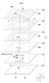
- FIG. 1 is an exploded perspective view of a multilayer substrate 10.
- FIG. FIG. 2 is an exploded perspective view of the multilayer substrate 10a.
- FIG. 3 is an exploded perspective view of the multilayer substrate 10b.
- FIG. 4 is an exploded perspective view of the multilayer substrate 10c.
- FIG. 5 is an exploded perspective view of the multilayer substrate 10d.
- FIG. 6 is a rear view of the multilayer board 10d.
- the stacking direction of the laminate 12 is parallel to the up-down axis.
- the up-down axis coincides with the Z axis.
- the up direction is the positive direction of the Z axis.
- the down direction is the negative direction of the Z axis.
- two sides of the laminate 12 extend along the left-right axis.
- the remaining two sides of the laminate 12 extend along the front-rear axis.
- the left-right axis is perpendicular to the up-down axis.
- the front-rear axis is perpendicular to both the up-down axis and the left-right axis.
- the multilayer substrate 10 is used, for example, in a wireless communication terminal such as a smartphone. As shown in FIG. 1, the multilayer substrate 10 includes a laminate 12, a radiation conductor layer 16, a first ground conductor layer 28, second ground conductor layers 30a to 30d, a current path R, and a branch conductor layer 22.
- the laminate 12 has a plate shape. As shown in FIG. 1, the laminate 12 has a rectangular shape when viewed from below.
- the laminate 12 has a structure in which the insulator layers 14a to 14f are stacked along the vertical axis (Z-axis).
- the insulator layers 14a to 14f are arranged in this order from top to bottom.
- the insulator layers 14a to 14f are made of a thermoplastic resin such as polyimide or liquid crystal polymer. Adjacent insulator layers 14a to 14f are fused together.
- the laminate 12 is flexible.
- the radiating conductor layer 16 emits and/or receives high-frequency signals.
- the radiating conductor layer 16 is provided on the laminate 12.
- the radiating conductor layer 16 is located on the upper main surface of the insulator layer 14a.
- the radiating conductor layer 16 has a rectangular shape when viewed from below.
- the radiating conductor layer 16 has two sides extending along the front-to-back axis and two sides extending along the left-to-right axis when viewed from below.
- the first ground conductor layer 28 is provided on the laminate 12 as shown in FIG. 1. More specifically, the first ground conductor layer 28 is located below the radiation conductor layer 16 (negative side of the Z axis). The first ground conductor layer 28 is provided on the lower main surface of the insulator layer 14f. As shown in FIG. 1, the first ground conductor layer 28 has a rectangular shape when viewed from below. The first ground conductor layer 28 covers substantially the entire lower main surface of the insulator layer 14f. As a result, the first ground conductor layer 28 overlaps with the radiation conductor layer 16 when viewed from the downward direction (negative direction of the Z axis). The first ground conductor layer 28 is connected to a ground potential. As a result, the radiation conductor layer 16 and the first ground conductor layer 28 form a patch antenna.
- the second ground conductor layers 30a to 30d are provided on the laminate 12 as shown in FIG. 1. More specifically, the second ground conductor layers 30a to 30d are located above the first ground conductor layer 28 (on the positive side of the Z axis). In this embodiment, the second ground conductor layers 30a to 30d are located on the upper main surfaces of the insulator layers 14a to 14d, respectively.
- the second ground conductor layers 30a to 30d are located near the radiation conductor layer 16. Specifically, when viewed from below (the negative direction of the Z axis), there are no ground conductor layers other than the first ground conductor layer 28 between the radiation conductor layer 16 and the second ground conductor layers 30a to 30d. The second ground conductor layers 30a to 30d are connected to the ground potential.
- a high-frequency signal is transmitted through the current path R.
- the current path R is formed by a conductor connecting the external electrode 24 and the radiation conductor layer 16.
- the current path R is provided in the laminate 12.
- the current path R is connected to the radiation conductor layer 16.
- the current path R includes the signal conductor layer 20 and the interlayer connection conductors v1 and v2.
- the signal conductor layer 20 is provided in the laminate 12.
- the signal conductor layer 20 is located below the radiation conductor layer 16 (negative side of the Z axis).
- the signal conductor layer 20 is located above the first ground conductor layer 28 (positive side of the Z axis).
- the signal conductor layer 20 is located on the upper main surface of the insulator layer 14e.
- the signal conductor layer 20 includes a first portion 20a and a second portion 20b.
- the first portion 20a extends along the front-to-rear axis.
- the second portion 20b extends along the left-to-right axis. When viewed from below, the front end of the first portion 20a overlaps with the radiating conductor layer 16. The rear end of the first portion 20a is connected to the right end of the second portion 20b.
- the external electrode 24 is provided on the lower main surface of the insulator layer 14f.
- the external electrode 24 is not in contact with the first ground conductor layer 28. Therefore, the external electrode 24 is located within an opening provided in the first ground conductor layer 28. When viewed from below, the external electrode 24 overlaps with the left end of the second portion. A high-frequency signal is input to or output from the external electrode 24.
- the interlayer connection conductor v1 electrically connects the radiation conductor layer 16 and the signal conductor layer 20. More specifically, the interlayer connection conductor v1 penetrates the insulator layers 14a to 14d along the up-down axis. The upper end of the interlayer connection conductor v1 contacts the radiation conductor layer 16 at the power supply point P1. The lower end of the interlayer connection conductor v1 contacts the front end of the first portion 20a.
- the interlayer connection conductor v2 electrically connects the signal conductor layer 20 and the external electrode 24. More specifically, the interlayer connection conductor v2 penetrates the insulator layers 14e and 14f along the up-down axis. The upper end of the interlayer connection conductor v2 contacts the left end of the second portion 20b. The lower end of the interlayer connection conductor v2 contacts the external electrode 24.
- the interlayer connection conductors v3 to v5 electrically connect the first ground conductor layer 28 and the second ground conductor layers 30a to 30d. More specifically, the interlayer connection conductors v3 to v5 penetrate the insulator layers 14a to 14f along the up-down axis. The upper ends of the interlayer connection conductors v3 to v5 are in contact with the second ground conductor layer 30a. The lower ends of the interlayer connection conductors v3 to v5 are in contact with the first ground conductor layer 28. Furthermore, the middle parts of the interlayer connection conductors v3 to v5 are in contact with the second ground conductor layers 30b to 30d.
- the branch conductor layer 22 is provided in the laminate 12.
- the branch conductor layer 22 is located below the second ground conductor layers 30a to 30d (negative side of the Z axis).
- the branch conductor layer 22 is located on the upper main surface of the insulator layer 14e.
- the branch conductor layer 22 branches off from the current path R. More specifically, the branch conductor layer 22 extends rightward from the rear end of the first portion 20a and the right end of the second portion 20b. Therefore, when viewed in the downward direction, the branch conductor layer 22 has a linear shape. When viewed in the downward direction (negative side of the Z axis), at least a portion of the branch conductor layer 22 overlaps with the second ground conductor layers 30a to 30d.
- the branch conductor layer 22 when viewed in the downward direction, the entire branch conductor layer 22 overlaps with the second ground conductor layers 30a to 30d. Therefore, when viewed downward (negative direction of the Z axis), the connection portion between the branch conductor layer 22 and the current path R overlaps with the second ground conductor layers 30a to 30d. However, when viewed downward (negative direction of the Z axis), the branch conductor layer 22 does not overlap with the radiation conductor layer 16. Such a branch conductor layer 22 is an open stub. Therefore, the branch conductor layer 22 is not connected to any conductor layer other than the signal conductor layer 20.
- the above-mentioned radiation conductor layer 16, signal conductor layer 20, branch conductor layer 22, external electrode 24, first ground conductor layer 28, and second ground conductor layers 30a to 30d are formed by patterning metal foil attached to the upper or lower principal surfaces of the insulator layers 14a to 14f.
- the metal foil is, for example, copper foil.
- the interlayer connection conductors v1 to v5 are formed by filling conductive paste into through holes that penetrate the insulator layers 14a to 14f along the vertical axis, and solidifying the conductive paste by heating and pressurizing.
- the multilayer substrate 10 can suppress coupling between the branch conductor layer 22 and the radiation conductor layer 16. More specifically, when viewed from below, at least a portion of the branch conductor layer 22 overlaps with the second ground conductor layers 30a-30d. This allows the second ground conductor layers 30a-30d to be located between the radiation conductor layer 16 and the branch conductor layer 22. As a result, the multilayer substrate 10 can suppress coupling between the branch conductor layer 22 and the radiation conductor layer 16.
- connection portion between the branch conductor layer 22 and the current path R overlaps with the second ground conductor layers 30a to 30d. This makes it possible to more effectively suppress coupling between the branch conductor layer 22 and the radiation conductor layer 16.
- the entire branch conductor layer 22 overlaps with the second ground conductor layers 30a to 30d. This makes it possible to more effectively suppress coupling between the branch conductor layer 22 and the radiation conductor layer 16.
- the branch conductor layer 22 when viewed from below, does not overlap with the radiation conductor layer 16. This makes it possible to more effectively suppress coupling between the branch conductor layer 22 and the radiation conductor layer 16.
- the branch conductor layer 22 branches off from the current path R.
- the branch conductor layer 22 plays a role in matching the characteristic impedance generated in the radiating conductor layer 16 with the characteristic impedance generated in the current path R.
- the reflection of high-frequency signals at the boundary between the radiating conductor layer 16 and the current path R is suppressed, and the loss of high-frequency signals is reduced.
- the branch conductor layer 22 is not far away from the radiating conductor layer 16 for the following reasons. Reflection of the high-frequency signal occurs at the power supply point P1. The reflected high-frequency signal is reflected again at the branch conductor layer 22. The reflected wave is radiated as an electromagnetic wave from the radiating conductor layer 16. In this way, in the multilayer substrate 10, the reflected wave is used as an electromagnetic wave of the high-frequency signal.
- the branch conductor layer 22 is far away from the radiating conductor layer 16, loss occurs in the reflected wave between the branch conductor layer 22 and the radiating conductor layer 16. Therefore, it is preferable that the branch conductor layer 22 is not far away from the radiating conductor layer 16. This improves the gain of the radiating conductor layer 16.
- the second ground conductor layers 30a-30d do not overlap the radiating conductor layer 16 when viewed from below, and are located above the first ground conductor layer 28.
- the radiation pattern and reception pattern of the radiating conductor layer 16 are less likely to spread in the direction approaching the first ground conductor layer 28. This improves the directivity of the radiation pattern and reception pattern of the radiating conductor layer 16.
- the second ground conductor layers 30a to 30d when viewed from below, have a ring shape that surrounds the radiation conductor layer 16. This further improves the directivity of the radiation pattern and reception pattern of the radiation conductor layer 16.
- the distance D1 between the signal conductor layer 20 and the first ground conductor layer 28 on the vertical axis (Z axis) is shorter than the distance D2 between the signal conductor layer 20 and the radiating conductor layer 16 on the vertical axis (Z axis). This prevents the signal conductor layer 20 from coupling to the radiating conductor layer 16.
- FIG. 2 is an exploded perspective view of the multilayer substrate 10a.
- the multilayer substrate 10a differs from the multilayer substrate 10 in the shape of the second ground conductor layers 30a-30d. More specifically, when viewed from below, the second ground conductor layers 30a-30d have an angular C-shape. When viewed from below, the second ground conductor layers 30a-30d do not have a front edge. In this way, when viewed from below, the second ground conductor layers 30a-30d do not have to have a ring shape surrounding the radiation conductor layer 16.
- the rest of the structure of the multilayer substrate 10a is the same as that of the multilayer substrate 10, so a description will be omitted.
- the multilayer substrate 10a can achieve the same effects as the multilayer substrate 10.
- Fig. 3 is an exploded perspective view of the multilayer substrate 10b.
- the multilayer substrate 10b differs from the multilayer substrate 10 in the following respects.
- the multilayer substrate 10b does not include the second ground conductor layer 30d.
- the multilayer substrate 10b further includes an interlayer connection conductor v11.
- the first portion 20a and the second portion 20b are provided in different insulating layers.
- the first portion 20a is located on the upper main surface of the insulator layer 14d.
- the second portion 20b is located on the upper main surface of the insulator layer 14e.
- the interlayer connection conductor v11 penetrates the insulator layer 14d along the vertical axis (Z-axis).
- the upper end of the interlayer connection conductor v11 contacts the rear end of the first portion 20a.
- the lower end of the interlayer connection conductor v11 contacts the right end of the second portion 20b and the left end of the branch conductor layer 22.
- the branch conductor layer 22 is connected to the interlayer connection conductor v11.
- the rest of the structure of the multilayer board 10b is the same as that of the multilayer board 10, so a description will be omitted.
- the multilayer board 10b can achieve the same effects as the multilayer board 10.
- Fig. 4 is an exploded perspective view of the multilayer substrate 10c.
- the multilayer board 10c differs from the multilayer board 10 in that it further includes an interlayer connection conductor v12.
- the interlayer connection conductor v12 electrically connects the branch conductor layer 22 and the first ground conductor layer 28. Specifically, the interlayer connection conductor v12 penetrates the insulator layers 14e and 14f along the up-down axis. The upper end of the interlayer connection conductor v12 contacts the right end of the branch conductor layer 22. The lower end of the interlayer connection conductor v12 contacts the first ground conductor layer 28. This makes the branch conductor layer 22 a short stub.
- the rest of the structure of the multilayer board 10c is the same as that of the multilayer board 10, so a description will be omitted.
- the multilayer board 10c can achieve the same effects as the multilayer board 10.
- FIG. 5 is an exploded perspective view of the multilayer substrate 10d.
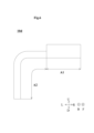
- Fig. 6 is a rear view of the multilayer substrate 10d.
- the multilayer board 10d differs from the multilayer board 10 in that it has a first section A1 and a second section A2. More specifically, the first section A1 is provided with a radiation conductor layer 16 and second ground conductor layers 30a-30d. The second section A2 is provided with a signal conductor layer 20 and a first ground conductor layer 28. The second section A2 has a band shape that extends along the signal conductor layer 20. The first section A1 is not bent. The second section A2 is bent. The rest of the structure of the multilayer board 10d is the same as that of the multilayer board 10, so a description will be omitted. The multilayer board 10d can achieve the same effects as the multilayer board 10.
- the multilayer board according to the present invention is not limited to the multilayer boards 10, 10a to 10d, and may be modified within the scope of the invention.
- the structures of the multilayer boards 10, 10a to 10d may be combined in any manner.
- the interlayer connection conductors v11 and v12 may pass through multiple insulating layers.
- connection portion between the branch conductor layer 22 and the current path R does not have to overlap with the second ground conductor layers 30a to 30d.
- a portion of the branch conductor layer 22 may overlap with the second ground conductor layers 30a to 30d.
- the branch conductor layer 22 may overlap the radiating conductor layer 16.
- the branched conductor layer 22 does not have to have a linear shape.
- the branched conductor layer 22 may have, for example, a circular or square shape.
- the multilayer substrate 10, 10a to 10d may have a feed point P2 in addition to the feed point P1.
- the electromagnetic field vibration direction of the high-frequency signal fed at the feed point P2 is different from the electromagnetic field vibration direction of the high-frequency signal fed at the feed point P1.
- a third ground conductor layer may be provided on the signal conductor layer 20.
- the multilayer substrate 10, 10a to 10d may include at least one of the second ground conductor layers 30a to 30d.
- each of the second ground conductor layers 30a to 30d may include multiple conductor layers arranged at intervals on a circular track surrounding the periphery of the radiation conductor layer 16 when viewed in the downward direction.
- the present invention has the following structure:
- the laminate has a structure in which a plurality of insulating layers are laminated along the Z axis, the radiating conductor layer is provided on the laminate, the first ground conductor layer is provided in the laminate, overlaps the radiation conductor layer when viewed in the negative direction of the Z axis, and is located on the negative side of the Z axis with respect to the radiation conductor layer; the second ground conductor layer is provided on the laminate, does not overlap the radiation conductor layer when viewed in the negative direction of the Z axis, and is located on the positive side of the Z axis with respect to the first ground conductor layer; When viewed in the negative direction of the Z axis, there is no ground conductor layer other than the first ground conductor layer between the radiation conductor layer and the second ground conductor layer, the current path is provided in the laminate and is connected to the radiation conductor layer; the branch
- a multilayer substrate according to (1) When viewed in the negative direction of the Z axis, a connection portion between the branch conductor layer and the current path overlaps with the second ground conductor layer.
- the branch conductor layer does not overlap with the radiation conductor layer.
- a multilayer substrate according to any one of (1) to (3).
- the current path includes an interlayer connection conductor; the interlayer connection conductor penetrates at least one of the plurality of insulating layers along the Z-axis;
- the branch conductor layer is connected to the interlayer connection conductor.
- a multilayer substrate according to any one of (1) to (4).
- the second ground conductor layer When viewed in the negative direction of the Z axis, the second ground conductor layer has a ring shape surrounding the radiation conductor layer.
- a multilayer substrate according to any one of (1) to (5).
- the current path includes a signal conductor layer; the signal conductor layer is provided in the laminate, and is located on the negative side of the Z axis with respect to the radiation conductor layer, and is located on the positive side of the Z axis with respect to the first ground conductor layer; a distance in the Z-axis direction between the signal conductor layer and the first ground conductor layer is shorter than a distance in the Z-axis direction between the signal conductor layer and the radiation conductor layer;
- a multilayer substrate according to any one of (1) to (6).
- the branched conductor layer is an open stub.
- the branch conductor layer is a short stub.
- Multilayer substrate 12 Laminated bodies 14a to 14f: Insulator layer 16: Radiating conductor layer 20: Signal conductor layer 20a: First portion 20b: Second portion 22: Branch conductor layer 24: External electrode 28: First ground conductor layer 30a to 30d: Second ground conductor layer A1: First section A2: Second section P1, P2: Power supply point R: Current paths v1 to v5, v11, v12: Interlayer connection conductors
Landscapes
- Engineering & Computer Science (AREA)
- Manufacturing & Machinery (AREA)
- Microelectronics & Electronic Packaging (AREA)
- Structure Of Printed Boards (AREA)
- Production Of Multi-Layered Print Wiring Board (AREA)
Priority Applications (3)
| Application Number | Priority Date | Filing Date | Title |
|---|---|---|---|
| CN202390000694.1U CN224153581U (zh) | 2023-01-11 | 2023-11-28 | 多层基板 |
| JP2024570073A JP7803439B2 (ja) | 2023-01-11 | 2023-11-28 | 多層基板 |
| US19/256,811 US20250329932A1 (en) | 2023-01-11 | 2025-07-01 | Multilayer substrate |
Applications Claiming Priority (2)
| Application Number | Priority Date | Filing Date | Title |
|---|---|---|---|
| JP2023-002194 | 2023-01-11 | ||
| JP2023002194 | 2023-01-11 |
Related Child Applications (1)
| Application Number | Title | Priority Date | Filing Date |
|---|---|---|---|
| US19/256,811 Continuation US20250329932A1 (en) | 2023-01-11 | 2025-07-01 | Multilayer substrate |
Publications (1)
| Publication Number | Publication Date |
|---|---|
| WO2024150551A1 true WO2024150551A1 (ja) | 2024-07-18 |
Family
ID=91896706
Family Applications (1)
| Application Number | Title | Priority Date | Filing Date |
|---|---|---|---|
| PCT/JP2023/042580 Ceased WO2024150551A1 (ja) | 2023-01-11 | 2023-11-28 | 多層基板 |
Country Status (4)
| Country | Link |
|---|---|
| US (1) | US20250329932A1 (https=) |
| JP (1) | JP7803439B2 (https=) |
| CN (1) | CN224153581U (https=) |
| WO (1) | WO2024150551A1 (https=) |
Citations (4)
| Publication number | Priority date | Publication date | Assignee | Title |
|---|---|---|---|---|
| JP2019009544A (ja) * | 2017-06-22 | 2019-01-17 | Tdk株式会社 | デュアルバンドパッチアンテナ |
| WO2019188471A1 (ja) * | 2018-03-30 | 2019-10-03 | 株式会社村田製作所 | アンテナモジュールおよびそれを搭載した通信装置 |
| WO2022064864A1 (ja) * | 2020-09-24 | 2022-03-31 | 株式会社村田製作所 | アンテナ素子 |
| WO2022234748A1 (ja) * | 2021-05-07 | 2022-11-10 | 株式会社村田製作所 | アンテナ素子、電子機器及びアンテナ素子の製造方法 |
-
2023
- 2023-11-28 JP JP2024570073A patent/JP7803439B2/ja active Active
- 2023-11-28 WO PCT/JP2023/042580 patent/WO2024150551A1/ja not_active Ceased
- 2023-11-28 CN CN202390000694.1U patent/CN224153581U/zh active Active
-
2025
- 2025-07-01 US US19/256,811 patent/US20250329932A1/en active Pending
Patent Citations (4)
| Publication number | Priority date | Publication date | Assignee | Title |
|---|---|---|---|---|
| JP2019009544A (ja) * | 2017-06-22 | 2019-01-17 | Tdk株式会社 | デュアルバンドパッチアンテナ |
| WO2019188471A1 (ja) * | 2018-03-30 | 2019-10-03 | 株式会社村田製作所 | アンテナモジュールおよびそれを搭載した通信装置 |
| WO2022064864A1 (ja) * | 2020-09-24 | 2022-03-31 | 株式会社村田製作所 | アンテナ素子 |
| WO2022234748A1 (ja) * | 2021-05-07 | 2022-11-10 | 株式会社村田製作所 | アンテナ素子、電子機器及びアンテナ素子の製造方法 |
Also Published As
| Publication number | Publication date |
|---|---|
| US20250329932A1 (en) | 2025-10-23 |
| CN224153581U (zh) | 2026-04-21 |
| JPWO2024150551A1 (https=) | 2024-07-18 |
| JP7803439B2 (ja) | 2026-01-21 |
Similar Documents
| Publication | Publication Date | Title |
|---|---|---|
| JP6750738B2 (ja) | アンテナモジュールおよび通信装置 | |
| JP5495335B2 (ja) | アンテナユニット | |
| CN110854548B (zh) | 天线结构及具有该天线结构的无线通信装置 | |
| TW201842712A (zh) | 高頻模組 | |
| WO2011021677A1 (ja) | アンテナモジュール | |
| WO2019208022A1 (ja) | アンテナモジュールおよびそれを搭載した通信装置 | |
| US12046838B2 (en) | Multilayer board | |
| US20250118897A1 (en) | Electronic device and multilayer substrate | |
| JP7803439B2 (ja) | 多層基板 | |
| US20250038413A1 (en) | Multilayer substrate | |
| JP7750263B2 (ja) | 多層基板 | |
| US20180191082A1 (en) | Wideband antenna array on laminated printed circuit board | |
| JP2019016929A (ja) | 多層基板型アレイアンテナ | |
| US12620712B2 (en) | Multilayer board and antenna module | |
| JP6890155B2 (ja) | アレイアンテナ | |
| JP7794328B2 (ja) | 多層基板 | |
| US20240088565A1 (en) | Multilayer board and antenna module | |
| JP2019114938A (ja) | アンテナモジュール | |
| CN220895843U (zh) | 多层基板及天线模块 | |
| JP7845285B2 (ja) | 多層基板及びアンテナモジュール | |
| JP7810309B2 (ja) | アンテナ部品 | |
| JP6493879B2 (ja) | アンテナ装置 | |
| CN220653600U (zh) | 多层基板 | |
| US20240422913A1 (en) | Circuit module and circuit board | |
| CN223024647U (zh) | 多层基板 |
Legal Events
| Date | Code | Title | Description |
|---|---|---|---|
| 121 | Ep: the epo has been informed by wipo that ep was designated in this application |
Ref document number: 23916167 Country of ref document: EP Kind code of ref document: A1 |
|
| WWE | Wipo information: entry into national phase |
Ref document number: 2024570073 Country of ref document: JP |
|
| NENP | Non-entry into the national phase |
Ref country code: DE |
|
| 122 | Ep: pct application non-entry in european phase |
Ref document number: 23916167 Country of ref document: EP Kind code of ref document: A1 |