WO2024150293A1 - 量子変換器及び量子変換方法 - Google Patents
量子変換器及び量子変換方法 Download PDFInfo
- Publication number
- WO2024150293A1 WO2024150293A1 PCT/JP2023/000372 JP2023000372W WO2024150293A1 WO 2024150293 A1 WO2024150293 A1 WO 2024150293A1 JP 2023000372 W JP2023000372 W JP 2023000372W WO 2024150293 A1 WO2024150293 A1 WO 2024150293A1
- Authority
- WO
- WIPO (PCT)
- Prior art keywords
- ferromagnetic
- topological insulator
- insulator film
- quantum
- film
- Prior art date
- Legal status (The legal status is an assumption and is not a legal conclusion. Google has not performed a legal analysis and makes no representation as to the accuracy of the status listed.)
- Ceased
Links
Images


Classifications
-
- G—PHYSICS
- G06—COMPUTING OR CALCULATING; COUNTING
- G06N—COMPUTING ARRANGEMENTS BASED ON SPECIFIC COMPUTATIONAL MODELS
- G06N10/00—Quantum computing, i.e. information processing based on quantum-mechanical phenomena
- G06N10/40—Physical realisations or architectures of quantum processors or components for manipulating qubits, e.g. qubit coupling or qubit control
-
- G—PHYSICS
- G02—OPTICS
- G02F—OPTICAL DEVICES OR ARRANGEMENTS FOR THE CONTROL OF LIGHT BY MODIFICATION OF THE OPTICAL PROPERTIES OF THE MEDIA OF THE ELEMENTS INVOLVED THEREIN; NON-LINEAR OPTICS; FREQUENCY-CHANGING OF LIGHT; OPTICAL LOGIC ELEMENTS; OPTICAL ANALOGUE/DIGITAL CONVERTERS
- G02F1/00—Devices or arrangements for the control of the intensity, colour, phase, polarisation or direction of light arriving from an independent light source, e.g. switching, gating or modulating; Non-linear optics
- G02F1/01—Devices or arrangements for the control of the intensity, colour, phase, polarisation or direction of light arriving from an independent light source, e.g. switching, gating or modulating; Non-linear optics for the control of the intensity, phase, polarisation or colour
- G02F1/09—Devices or arrangements for the control of the intensity, colour, phase, polarisation or direction of light arriving from an independent light source, e.g. switching, gating or modulating; Non-linear optics for the control of the intensity, phase, polarisation or colour based on magneto-optical elements, e.g. exhibiting Faraday effect
-
- G—PHYSICS
- G02—OPTICS
- G02F—OPTICAL DEVICES OR ARRANGEMENTS FOR THE CONTROL OF LIGHT BY MODIFICATION OF THE OPTICAL PROPERTIES OF THE MEDIA OF THE ELEMENTS INVOLVED THEREIN; NON-LINEAR OPTICS; FREQUENCY-CHANGING OF LIGHT; OPTICAL LOGIC ELEMENTS; OPTICAL ANALOGUE/DIGITAL CONVERTERS
- G02F1/00—Devices or arrangements for the control of the intensity, colour, phase, polarisation or direction of light arriving from an independent light source, e.g. switching, gating or modulating; Non-linear optics
- G02F1/35—Non-linear optics
- G02F1/353—Frequency conversion, i.e. wherein a light beam is generated with frequency components different from those of the incident light beams
-
- G—PHYSICS
- G02—OPTICS
- G02F—OPTICAL DEVICES OR ARRANGEMENTS FOR THE CONTROL OF LIGHT BY MODIFICATION OF THE OPTICAL PROPERTIES OF THE MEDIA OF THE ELEMENTS INVOLVED THEREIN; NON-LINEAR OPTICS; FREQUENCY-CHANGING OF LIGHT; OPTICAL LOGIC ELEMENTS; OPTICAL ANALOGUE/DIGITAL CONVERTERS
- G02F2/00—Demodulating light; Transferring the modulation of modulated light; Frequency-changing of light
- G02F2/02—Frequency-changing of light, e.g. by quantum counters
-
- G—PHYSICS
- G06—COMPUTING OR CALCULATING; COUNTING
- G06N—COMPUTING ARRANGEMENTS BASED ON SPECIFIC COMPUTATIONAL MODELS
- G06N10/00—Quantum computing, i.e. information processing based on quantum-mechanical phenomena
Definitions
- This disclosure relates to a quantum converter and a quantum conversion method.
- Quantum converters for quantum conversion have also been proposed.
- the objective of this disclosure is to provide a quantum converter and a quantum conversion method that can improve conversion efficiency.
- a quantum converter includes a ferromagnetic topological insulator film having a first surface, a magnetic field application unit that applies a magnetic field including a component perpendicular to the first surface to the ferromagnetic topological insulator film, and a microwave transceiver unit that transmits and receives microwaves between the ferromagnetic topological insulator film, and in which laser light is irradiated onto the first surface of the ferromagnetic topological insulator film.
- This disclosure makes it possible to improve conversion efficiency.
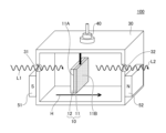
- FIG. 1 is a schematic diagram showing a quantum converter according to a first embodiment.
- FIG. 2 is a schematic diagram showing a quantum converter according to a reference example.
- FIG. 3 is a diagram showing the relationship between the thickness of a ferromagnetic topological insulator film and the ratio of conversion efficiencies.
- FIG. 4 is a diagram showing the relationship between the thickness of a ferromagnetic topological insulator film, the atomic ratio of the ferromagnetic material, and the ratio of the conversion efficiency.
- FIG. 5 is a schematic diagram showing a quantum converter according to the second embodiment.
- FIG. 6 is a schematic diagram showing a quantum converter according to the third embodiment.
- FIG. 1 is a schematic diagram showing a quantum converter according to the first embodiment.
- the quantum converter 100 has a microwave resonator 30, a laminate 10, a south pole 51, a north pole 52, and an antenna 40.
- the laminate 10 includes a ferromagnetic topological insulator film 11 and a first film 12.
- the ferromagnetic topological insulator film 11 includes a first surface 11A and a second surface 11B opposite to the first surface 11A.
- the first film 12 is in contact with the first surface 11A.
- the first film 12 is made of, for example, a nonmagnetic insulator.
- the first film 12 is a substrate including, for example, SrTiO 3 , InP, or Al 2 O 3 , or any combination thereof.
- the ferromagnetic topological insulator film 11 includes a topological insulator and a ferromagnetic material doped into the topological insulator.
- the topological insulator includes Bi, Sb, and Te
- the ferromagnetic material includes Cr or V, or both of these.
- the composition of the ferromagnetic topological insulator film 11 is, for example, Crx (Bi1 - ySby ) 2-xTe3 or Vx (Bi1 - ySby ) 2-xTe3 .
- the value of x is 0.1 or more and 0.6 or less
- the value of y is 0.7 or more and 0.9 or less.
- the thickness of the ferromagnetic topological insulator film 11 is, for example, 5 nm or more and 100 ⁇ m or less.
- the ferromagnetic topological insulator film 11 has a square planar shape with a side length of about 1 mm when viewed from a direction perpendicular to the first surface 11A.
- the planar shape of the ferromagnetic topological insulator film 11 is not limited to a square shape, and may be a circle or the like.
- the south pole 51 and north pole 52 are provided on the outer wall surface of the microwave resonator 30.
- the south pole 51 faces the first surface 11A
- the north pole 52 faces the second surface 11B.
- a magnetic field H is generated between the south pole 51 and the north pole 52, oriented from the south pole 51 to the north pole 52.
- the south pole 51 and the north pole 52 act as magnetic field application units and apply a magnetic field H including a component perpendicular to the first surface 11A to the ferromagnetic topological insulator film 11.
- the antenna 40 is provided on the outer wall surface of the microwave resonator 30.
- the antenna 40 serves as a microwave transmitting/receiving unit, transmitting and receiving microwaves between the ferromagnetic topological insulator film 11.
- the microwave resonator 30 is provided with an inlet 31 and an outlet 32.
- the inlet 31 faces the first surface 11A
- the outlet 32 faces the second surface 11B.
- An optical fiber is connected to the inlet 31, and laser light L1 is irradiated from the outside toward the ferromagnetic topological insulator film 11 through the inlet 31.
- the laser light L1 is irradiated toward the first surface 11A of the ferromagnetic topological insulator film 11.
- An optical fiber is connected to the outlet 32, and the laser light L2 that has passed through the ferromagnetic topological insulator film 11 is output to the outside through the outlet 32.
- the laser light L1 is linearly polarized laser light.
- the polarization and other properties of the laser light L2 outputted to the outside through the output port 32 are detected.
- the microwave photons of the microwaves irradiated to the ferromagnetic topological insulator film 11 through the antenna 40 are quantum converted into optical photons.
- the photon conversion efficiency ⁇ of a ferromagnetic material utilizing the Faraday effect is approximately expressed as “ ⁇ F 2 /N S 2 ,” where “ ⁇ F ” is the Faraday rotation angle, and “N S ” is the total number of spins contained in the ferromagnetic material.
- the Faraday rotation angle ⁇ F in a ferromagnetic topological insulator film is expressed as "tan -1 ⁇ (rad)."
- ⁇ is the fine structure constant, and the value of "tan -1 ⁇ (rad),” that is, the Faraday rotation angle ⁇ F , is approximately 1/137 rad.
- the total number of spins N S contained in the ferromagnetic topological insulator film 11 is "n S ⁇ V," where n S (mm -3 ) is the spin density per unit volume of the ferromagnetic topological insulator film 11 and V (mm 3 ) is the volume of the ferromagnetic topological insulator film 11.
- n S0 (mm -3 ) is the spin density per unit volume of the ferromagnetic material contained in the ferromagnetic topological insulator film 11 and ⁇ S is the atomic ratio of the ferromagnetic material in the ferromagnetic topological insulator film 11
- the spin density n S per unit volume of the ferromagnetic topological insulator film 11 is " ⁇ S ⁇ n S0 (mm -3 )."
- the spin density nS of the ferromagnetic topological insulator film 11 is calculated as follows.
- 40 atomic % is Bi or Sb .
- Cr0.15 ( Bi0.1Sb0.9 ) 1.85Te3 15 atomic % of Bi or Sb contained in ( Bi0.1Sb0.9 ) 2Te3 is replaced with Cr . Therefore, the atomic ratio of Cr in Cr0.15 ( Bi0.1Sb0.9 ) 1.85Te3 is 6 atomic %.
- the spin density nS of the ferromagnetic topological insulator film 11 having a composition of Cr0.15 ( Bi0.1Sb0.9 ) 1.85Te3 is "0.06 ⁇ nS0,Cr (mm -3 ) ".
- the conversion efficiency ⁇ TI of the ferromagnetic topological insulator film 11 having a composition of Cr0.15(Bi0.1Sb0.9)1.85Te3 is expressed as " (1/137) 2 /(0.06 ⁇ nS0,Cr ⁇ V ) 2 ".
- the spin density n S0,Cr is 2.1 ⁇ 10 19 mm ⁇ 3
- the thickness d of the ferromagnetic topological insulator film 11 is 30 nm and the area S of the first surface 11A is 1 mm 2
- the conversion efficiency ⁇ TI of the ferromagnetic topological insulator film 11 is approximately 1.14 ⁇ 10 ⁇ 2 .
- FIG. 2 is a schematic diagram showing a quantum converter according to the reference example.
- the quantum converter 100X of the reference example has a ferromagnetic sphere 10X instead of the laminate 10.
- the sphere 10X is made of yttrium iron garnet (YIG) and has a diameter of 0.75 mm.
- the south pole 51 and north pole 52 are arranged so that a magnetic field H is formed in a direction perpendicular to the traveling direction of the laser light L1.
- the other configurations are the same as those of the first embodiment.
- the Faraday rotation angle ⁇ F of the sphere 10X is expressed as " ⁇ d (rad)" where ⁇ is the Verdet constant and d is the diameter (mm).
- the Verdet constant of YIG is 0.38 (rad/mm).
- the total number of spins N S contained in the sphere 10X is "n S ⁇ V" when the spin density per unit volume of the sphere 10X is n S (mm -3 ) and the volume of the sphere 10X is V (mm 3 ).
- the entire sphere 10X is made of YIG, which is a ferromagnetic material, and the spin density n S is equal to the spin density per unit volume of the YIG, n S0 (mm -3 ).
- the conversion efficiency ⁇ of the sphere 10X made of YIG is expressed as "(0.38) 2 /(n S0,YIG ⁇ V) 2 .” Since the spin density n S0,YIG is 2.1 ⁇ 10 19 mm ⁇ 3 , when the volume V is 0.2209 mm 3 (diameter is 0.75 mm), the conversion efficiency ⁇ YIG of the sphere 10X is about 10 ⁇ 10 .
- the conversion efficiency ⁇ of the ferromagnetic topological insulator film 11 in the first embodiment is approximately 10 8 times larger than the conversion efficiency ⁇ YIG of the sphere 10X in the reference example.
- FIG. 3 is a diagram showing the relationship between the thickness d of the ferromagnetic topological insulator film 11 and the conversion efficiency ratio ( ⁇ TI / ⁇ YIG ).
- FIG. 3 shows the relationship when the atomic ratio ⁇ S of the ferromagnetic material is 1%, 6%, 25%, and 100%.
- FIG. 4 is a diagram showing the relationship between the thickness d of the ferromagnetic topological insulator film 11, the atomic ratio ⁇ S of the ferromagnetic material, and the conversion efficiency ratio ( ⁇ TI / ⁇ YIG ).
- the atomic ratio ⁇ S of the ferromagnetic material is constant, the smaller the thickness d of the ferromagnetic topological insulator film 11, the larger the conversion efficiency ratio ( ⁇ TI / ⁇ YIG ).
- the thickness d of the ferromagnetic topological insulator film 11 is constant, the smaller the atomic ratio of the ferromagnetic material ⁇ S , the larger the conversion efficiency ratio ( ⁇ TI / ⁇ YIG ).
- the conversion efficiency ratio ( ⁇ TI / ⁇ YIG ) is approximately 1 ⁇ 10 8 or more and 1 ⁇ 10 9 or less.
- the thickness d of the ferromagnetic topological insulator film 11 is less than 5 nm, the ferromagnetic topological insulator film 11 may behave as a two-dimensional material, making it difficult to obtain the Faraday effect. If the thickness d is 5 nm or more, the ferromagnetic topological insulator film 11 can be easily and stably formed.
- FIG. 5 is a schematic diagram showing a quantum converter according to the second embodiment.
- the quantum converter 200 according to the second embodiment has a stack 20 instead of the stack 10.
- the laminate 20 has multiple ferromagnetic topological insulator films 11 and multiple first films 12. Multiple ferromagnetic topological insulator films 11 and first films 12 are stacked alternately. Between two ferromagnetic topological insulator films 11 adjacent to each other in the stacking direction, the first surface 11A of one of the films faces the second surface 11B of the other film.
- the second embodiment can also obtain a high conversion efficiency, as in the first embodiment.
- the first embodiment when the spin density n S per unit volume of the ferromagnetic topological insulator film 11 is low, the total number of spins N S contained in the ferromagnetic topological insulator film 11 is small, and there is a possibility that a ferromagnetic resonance state (Kittel mode) cannot be realized.
- the second embodiment since a plurality of ferromagnetic topological insulator films 11 are stacked, even if the spin density n S is low, the total number of spins contained in the stack 10 can be sufficiently obtained, and a ferromagnetic resonance state can be realized.
- the conversion efficiency ⁇ TI in the second embodiment is expressed as "(n ⁇ F ) 2 /(n ⁇ N S ) 2 " when the number of ferromagnetic topological insulator films 11 is n, and is therefore " ⁇ F 2 /N S 2 ".
- the thickness of the first film 12 sandwiched between the two ferromagnetic topological insulator films 11 is, for example, less than or equal to the thickness d of the ferromagnetic topological insulator film 11.
- the third embodiment differs from the second embodiment mainly in the polarization of the laser light irradiated to the ferromagnetic topological insulator film 11.
- Fig. 6 is a schematic diagram showing a quantum converter according to the third embodiment.
- laser light L3 is irradiated from the outside toward the ferromagnetic topological insulator film 11 through an inlet 31.
- the laser light L3 includes two types of laser light whose deflection angles are orthogonal to each other.
- the laser light L3 is irradiated onto the first surface 11A of the ferromagnetic topological insulator film 11.
- An outlet 32 does not necessarily have to be provided.
- microwaves corresponding to the polarization of the laser light L3 are emitted from the laminate 20 and output to the outside through the antenna 40.
- the optical photons of the laser light L3 irradiated to the ferromagnetic topological insulator film 11 are quantum converted into microwave photons of microwaves.
- the third embodiment also provides high conversion efficiency, similar to the second embodiment.
- laminate 10 may be used instead of laminate 20.
- the quantum converter according to the present disclosure can be used, for example, for communication between superconducting quantum bits housed in each of a number of refrigerators.
- the use of the quantum converter according to the present disclosure is not limited to communication between superconducting quantum bits.
- the quantum converter can be used for quantum computing.
- Laminate 11 Ferromagnetic topological insulator film 11A: First surface 11B: Second surface 12: First film 20: Laminate 30: Microwave resonator 31: Inlet 32: Outlet 40: Antenna 51: South pole 52: North pole 100, 200, 300: Quantum converter
Landscapes
- Physics & Mathematics (AREA)
- General Physics & Mathematics (AREA)
- Engineering & Computer Science (AREA)
- Nonlinear Science (AREA)
- Theoretical Computer Science (AREA)
- Optics & Photonics (AREA)
- General Engineering & Computer Science (AREA)
- Pure & Applied Mathematics (AREA)
- Condensed Matter Physics & Semiconductors (AREA)
- Data Mining & Analysis (AREA)
- Evolutionary Computation (AREA)
- Mathematical Analysis (AREA)
- Mathematical Optimization (AREA)
- Computational Mathematics (AREA)
- Computing Systems (AREA)
- Artificial Intelligence (AREA)
- Mathematical Physics (AREA)
- Software Systems (AREA)
- Power Engineering (AREA)
- Thin Magnetic Films (AREA)
Priority Applications (3)
| Application Number | Priority Date | Filing Date | Title |
|---|---|---|---|
| PCT/JP2023/000372 WO2024150293A1 (ja) | 2023-01-11 | 2023-01-11 | 量子変換器及び量子変換方法 |
| EP23915917.1A EP4651040A4 (en) | 2023-01-11 | 2023-01-11 | QUANTUM CONVERTER AND QUANTUM CONVERSION METHOD |
| JP2024569710A JPWO2024150293A1 (https=) | 2023-01-11 | 2023-01-11 |
Applications Claiming Priority (1)
| Application Number | Priority Date | Filing Date | Title |
|---|---|---|---|
| PCT/JP2023/000372 WO2024150293A1 (ja) | 2023-01-11 | 2023-01-11 | 量子変換器及び量子変換方法 |
Publications (1)
| Publication Number | Publication Date |
|---|---|
| WO2024150293A1 true WO2024150293A1 (ja) | 2024-07-18 |
Family
ID=91896631
Family Applications (1)
| Application Number | Title | Priority Date | Filing Date |
|---|---|---|---|
| PCT/JP2023/000372 Ceased WO2024150293A1 (ja) | 2023-01-11 | 2023-01-11 | 量子変換器及び量子変換方法 |
Country Status (3)
| Country | Link |
|---|---|
| EP (1) | EP4651040A4 (https=) |
| JP (1) | JPWO2024150293A1 (https=) |
| WO (1) | WO2024150293A1 (https=) |
Cited By (1)
| Publication number | Priority date | Publication date | Assignee | Title |
|---|---|---|---|---|
| EP4693117A1 (en) * | 2024-08-08 | 2026-02-11 | Fujitsu Limited | Quantum transducer and quantum transduction method |
Citations (5)
| Publication number | Priority date | Publication date | Assignee | Title |
|---|---|---|---|---|
| JP2019512104A (ja) | 2016-02-08 | 2019-05-09 | インターナショナル・ビジネス・マシーンズ・コーポレーションInternational Business Machines Corporation | 歪み誘導型電気光学材料を有する集積マイクロ波−光単一フォトントランスデューサ |
| JP2019512161A (ja) | 2015-12-17 | 2019-05-09 | インターナショナル・ビジネス・マシーンズ・コーポレーションInternational Business Machines Corporation | Squidを利用する周波数変換装置および周波数変換装置を構成する方法 |
| US20210271999A1 (en) | 2019-10-02 | 2021-09-02 | International Business Machines Corporation | System and method to control quantum states of microwave frequency qubits with optical signals |
| WO2022137421A1 (ja) * | 2020-12-24 | 2022-06-30 | 富士通株式会社 | 量子ビット回路、量子コンピュータ及び量子ビット回路の製造方法 |
| US20220207405A1 (en) | 2020-12-29 | 2022-06-30 | Agency For Defense Development | Microwave-optic conversion system of quantum signals employing 3-dimensional microwave resonator and crystal oscillator |
Family Cites Families (1)
| Publication number | Priority date | Publication date | Assignee | Title |
|---|---|---|---|---|
| KR102619166B1 (ko) * | 2020-12-01 | 2023-12-27 | 국방과학연구소 | 광-마이크로파 양자 얽힘 광자쌍 생성 장치 및 그 방법, 이를 이용한 양자 레이더 |
-
2023
- 2023-01-11 JP JP2024569710A patent/JPWO2024150293A1/ja active Pending
- 2023-01-11 WO PCT/JP2023/000372 patent/WO2024150293A1/ja not_active Ceased
- 2023-01-11 EP EP23915917.1A patent/EP4651040A4/en active Pending
Patent Citations (5)
| Publication number | Priority date | Publication date | Assignee | Title |
|---|---|---|---|---|
| JP2019512161A (ja) | 2015-12-17 | 2019-05-09 | インターナショナル・ビジネス・マシーンズ・コーポレーションInternational Business Machines Corporation | Squidを利用する周波数変換装置および周波数変換装置を構成する方法 |
| JP2019512104A (ja) | 2016-02-08 | 2019-05-09 | インターナショナル・ビジネス・マシーンズ・コーポレーションInternational Business Machines Corporation | 歪み誘導型電気光学材料を有する集積マイクロ波−光単一フォトントランスデューサ |
| US20210271999A1 (en) | 2019-10-02 | 2021-09-02 | International Business Machines Corporation | System and method to control quantum states of microwave frequency qubits with optical signals |
| WO2022137421A1 (ja) * | 2020-12-24 | 2022-06-30 | 富士通株式会社 | 量子ビット回路、量子コンピュータ及び量子ビット回路の製造方法 |
| US20220207405A1 (en) | 2020-12-29 | 2022-06-30 | Agency For Defense Development | Microwave-optic conversion system of quantum signals employing 3-dimensional microwave resonator and crystal oscillator |
Non-Patent Citations (5)
| Title |
|---|
| HAMA, YUSUKE ET AL.: "8a-Z08-8 Nonlinear current on the surface of ferromagnetic topological insulator induced by spin pumping", LECTURE PREPRINTS OF THE 81ST JSAP AUTUMN MEETING, JAPAN SOCIETY OF APPLIED PHYSICS; [ONLINE VIRTUAL MEETING]; SEPTEMBER 9-11, 2020, JAPAN SOCIETY OF APPLIED PHYSICS, JP, vol. 81, 1 January 2020 (2020-01-01) - 11 September 2020 (2020-09-11), JP, pages 09 - 018, XP009556433 * |
| J. MACIEJKO ET AL., PHYS. REV. LETT., vol. 105, 2010, pages 166803 |
| R. HISATOMI, REV. B, vol. 93, 2016, pages 174427 |
| See also references of EP4651040A1 |
| TSE, MACDONALD, LETT., vol. 105, 2010, pages 057401 |
Cited By (1)
| Publication number | Priority date | Publication date | Assignee | Title |
|---|---|---|---|---|
| EP4693117A1 (en) * | 2024-08-08 | 2026-02-11 | Fujitsu Limited | Quantum transducer and quantum transduction method |
Also Published As
| Publication number | Publication date |
|---|---|
| EP4651040A4 (en) | 2026-03-18 |
| EP4651040A1 (en) | 2025-11-19 |
| JPWO2024150293A1 (https=) | 2024-07-18 |
Similar Documents
| Publication | Publication Date | Title |
|---|---|---|
| Kajale et al. | Field-free deterministic switching of all–van der Waals spin-orbit torque system above room temperature | |
| Sani et al. | Mutually synchronized bottom-up multi-nanocontact spin–torque oscillators | |
| Kamra et al. | Magnon-squeezing as a niche of quantum magnonics | |
| Qin et al. | In-plane critical magnetic fields in magic-angle twisted trilayer graphene | |
| Buddhiraju et al. | Nonreciprocal metamaterial obeying time-reversal symmetry | |
| Zhu et al. | Magnon-photon strong coupling for tunable microwave circulators | |
| US11011693B2 (en) | Integrated quantum circuit assemblies for cooling apparatus | |
| Ranzani et al. | Circulators at the quantum limit: Recent realizations of quantum-limited superconducting circulators and related approaches | |
| Kutsaev et al. | Up‐and‐coming advances in optical and microwave nonreciprocity: From classical to quantum realm | |
| US9767876B2 (en) | Magnonic holographic memory and methods | |
| JP3834616B2 (ja) | スピンフィルタ | |
| Sun et al. | Colossal anisotropic absorption of spin currents induced by chirality | |
| US20190131683A1 (en) | Multi-path interferometric josephson isolator based on nondegenerate three-wave mixing josephson devices | |
| WO2024150293A1 (ja) | 量子変換器及び量子変換方法 | |
| Ledwith et al. | Topological phase transitions and quantum Hall effect in the graphene family | |
| Dionne et al. | Circular polarization and nonreciprocal propagation in magnetic media | |
| Shuai et al. | Local anisotropy control of Pt/Co/Ir thin film with perpendicular magnetic anisotropy by surface acoustic waves | |
| EP2973995A1 (en) | Spin oscillator device | |
| Han et al. | Topological junctions in high-Chern-number quantum anomalous Hall systems | |
| Zheng et al. | Double-barrier magnetic tunnel junctions with enhanced tunnel magnetoresistance | |
| Zhang et al. | Spin-valley locking and pure spin-triplet superconductivity in noncollinear antiferromagnets proximitized to conventional superconductors | |
| Li et al. | Strain and stacking induced topological phase transition in bipolar ferromagnetic semiconductor OsClBr | |
| Chen et al. | Magnon confinement in a nanomagnonic waveguide by a magnetic Moiré superlattice | |
| Tahir et al. | Emergent flat band lattices in spatially periodic magnetic fields | |
| Han et al. | Topologically Protected and Highly Localized Surface Waves in Gyro‐Electromagnetic Metamaterials |
Legal Events
| Date | Code | Title | Description |
|---|---|---|---|
| 121 | Ep: the epo has been informed by wipo that ep was designated in this application |
Ref document number: 23915917 Country of ref document: EP Kind code of ref document: A1 |
|
| WWE | Wipo information: entry into national phase |
Ref document number: 2024569710 Country of ref document: JP |
|
| NENP | Non-entry into the national phase |
Ref country code: DE |
|
| WWP | Wipo information: published in national office |
Ref document number: 2023915917 Country of ref document: EP |