WO2024142183A1 - 光導波路素子、光変調器、および光送信装置 - Google Patents
光導波路素子、光変調器、および光送信装置 Download PDFInfo
- Publication number
- WO2024142183A1 WO2024142183A1 PCT/JP2022/048045 JP2022048045W WO2024142183A1 WO 2024142183 A1 WO2024142183 A1 WO 2024142183A1 JP 2022048045 W JP2022048045 W JP 2022048045W WO 2024142183 A1 WO2024142183 A1 WO 2024142183A1
- Authority
- WO
- WIPO (PCT)
- Prior art keywords
- electrode
- optical waveguide
- optical
- segment
- electrodes
- Prior art date
- Legal status (The legal status is an assumption and is not a legal conclusion. Google has not performed a legal analysis and makes no representation as to the accuracy of the status listed.)
- Ceased
Links
Images








Classifications
-
- G—PHYSICS
- G02—OPTICS
- G02F—OPTICAL DEVICES OR ARRANGEMENTS FOR THE CONTROL OF LIGHT BY MODIFICATION OF THE OPTICAL PROPERTIES OF THE MEDIA OF THE ELEMENTS INVOLVED THEREIN; NON-LINEAR OPTICS; FREQUENCY-CHANGING OF LIGHT; OPTICAL LOGIC ELEMENTS; OPTICAL ANALOGUE/DIGITAL CONVERTERS
- G02F1/00—Devices or arrangements for the control of the intensity, colour, phase, polarisation or direction of light arriving from an independent light source, e.g. switching, gating or modulating; Non-linear optics
- G02F1/01—Devices or arrangements for the control of the intensity, colour, phase, polarisation or direction of light arriving from an independent light source, e.g. switching, gating or modulating; Non-linear optics for the control of the intensity, phase, polarisation or colour
- G02F1/03—Devices or arrangements for the control of the intensity, colour, phase, polarisation or direction of light arriving from an independent light source, e.g. switching, gating or modulating; Non-linear optics for the control of the intensity, phase, polarisation or colour based on ceramics or electro-optical crystals, e.g. exhibiting Pockels effect or Kerr effect
- G02F1/035—Devices or arrangements for the control of the intensity, colour, phase, polarisation or direction of light arriving from an independent light source, e.g. switching, gating or modulating; Non-linear optics for the control of the intensity, phase, polarisation or colour based on ceramics or electro-optical crystals, e.g. exhibiting Pockels effect or Kerr effect in an optical waveguide structure
Definitions
- the present invention relates to an optical waveguide element, an optical modulator, and an optical transmitter.
- optical modulators incorporating an optical modulation element as an optical waveguide element composed of an optical waveguide formed on a substrate and a control electrode for controlling the light wave propagating through the optical waveguide are widely used.
- optical waveguide elements performing optical modulation semiconductor optical modulation elements using a semiconductor substrate such as an InP substrate and LN optical modulation elements using a LiNbO3 (hereinafter also referred to as LN) substrate have been put to practical use.
- the optical waveguide further includes a radio frequency electrode arranged on the optical substrate for modulating an optical wave propagating through the optical waveguide to perform a modulation operation
- the control electrode is a bias electrode that controls a bias point of the modulation operation.
- the auxiliary electrode is arranged such that the edge facing the segment electrode is closer to the segment electrode than a position which bisects the distance between the edge of the common electrode on the front optical waveguide side and the edge of the segment electrode on the optical waveguide side.
- the Mach-Zehnder type optical waveguides 37a, 37b, 37c, and 37d will be collectively referred to as the Mach-Zehnder type optical waveguide 37.
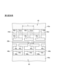
- Fig. 4 is a partial detailed view of part B of bias electrode portion 40 shown in Fig. 3.
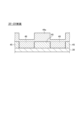
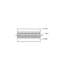
- Figs. 5 and 6 are a VV sectional view and a VI-VI sectional view of part B shown in Fig. 4.
- Part B in Fig. 4 shows the second control electrode 44 and the first control electrode 43 which face each other across one parallel waveguide 39b of the Mach-Zehnder type optical waveguide 37d.
- the other second control electrode 44 and the first control electrode 43 which face each other across the other parallel waveguide 39a in Fig. 3 are also configured in the same manner as shown in Fig. 4.
- each portion of the first control electrode 43 and the second control electrode 44 is formed directly on the optical substrate 30.
- the segment electrodes 43c, 44c arranged near the parallel waveguide 39 are divided along the extension direction of the parallel waveguide 39, so that it is possible to reduce substrate stress that may occur in the portion of the optical substrate 30 near the parallel waveguide 39, compared to a conventional bias electrode that is not divided.
- connection electrodes 43b and 44b may be connected to one end of each of the segment electrodes 43c and 44c in the longitudinal direction along the extension direction of the parallel waveguide 39.
- FIG. 7 is a diagram showing the configuration of the control electrode 42 of the light modulation element 3 according to the first modified example.
- FIG. 7 corresponds to FIG. 4 described above.
- the connection electrodes 43b and 44b are each connected to the left end of the segment electrodes 43c and 44c, respectively, in the longitudinal direction along the extension direction of the parallel waveguide 39.
- the first control electrode 43 and the second control electrode 44 that sandwich the parallel waveguide 39a can also be configured in a similar manner to the above.
- the auxiliary electrode 43d is arranged, for example, at a position where the side facing the segment electrode 43c is closer to the segment electrode 43c than the position that bisects the distance between the side of the common electrode 43a on the parallel waveguide 39 side and the side of the segment electrode 43c on the parallel waveguide 39 side.
- the auxiliary electrode 44d is arranged at a position where the side facing the segment electrode 44c is closer to the segment electrode 44c than the position that bisects the distance between the side of the common electrode 44a on the parallel waveguide 39 side and the side of the segment electrode 44c on the parallel waveguide 39 side.
- the auxiliary electrode 43d is arranged at a position where the line EL1, which is an extension of the side facing the segment electrode 43c, is closer to the segment electrode 43c than the line CL1, which indicates the position where the distance between the side of the common electrode 43a on the parallel waveguide 39b side and the side of the segment electrode 43c on the parallel waveguide 39b side is bisected.
- the auxiliary electrode 44d is arranged at a position where the line EL2, which is an extension of the side facing the segment electrode 44c, is closer to the segment electrode 44c than the line CL2, which indicates the position where the distance between the side of the common electrode 44a on the parallel waveguide 39b side and the side of the segment electrode 44c on the parallel waveguide 39b side is bisected.
- the first control electrode 43 and the second control electrode 44 on either side of the parallel waveguide 39a may be configured in the same manner as above.
- the auxiliary electrode 43d is arranged, for example, at a position where the side facing the segment electrode 43c is closer to the common electrode 43a than the position where the distance between the side of the common electrode 43a on the parallel waveguide 39 side and the side of the segment electrode 43c on the parallel waveguide 39 side is halved.
- the auxiliary electrode 44d is arranged at a position where the side facing the segment electrode 44c is closer to the common electrode 44a than the position where the distance between the side of the common electrode 44a on the parallel waveguide 39 side and the side of the segment electrode 44c on the parallel waveguide 39 side is halved.
- FIG. 9 is a diagram showing the configuration of the control electrode 42 of the light modulation element 3 according to the second modified example.
- FIG. 9 corresponds to FIG. 4 described above.
- the auxiliary electrode 43d is arranged at a position where the line EL1, which is an extension of the side facing the segment electrode 43c, is closer to the common electrode 43a than the line CL1, which indicates the position where the line EL1 bisects the distance between the side of the common electrode 43a on the parallel waveguide 39b side and the side of the segment electrode 43c on the parallel waveguide 39b side.
- the auxiliary electrode 44d is arranged at a position where the line EL2, which is an extension of the side facing the segment electrode 44c, is closer to the common electrode 44a than the line CL2, which indicates the position where the line EL2 bisects the distance between the side of the common electrode 44a on the parallel waveguide 39b side and the side of the segment electrode 44c on the parallel waveguide 39b side.
- the first control electrode 43 and the second control electrode 44 on either side of the parallel waveguide 39a can be configured in the same manner as above.
- the auxiliary electrodes 43d and 44d are formed closer to the common electrodes 43a and 44a, respectively, and away from the segment electrodes 43c and 44c, so that the substrate stress that may occur in the optical substrate 30 near the parallel waveguide 39 due to the auxiliary electrodes 43d and 44d can be reduced. Therefore, in the configuration shown in FIG. 9, the bias point fluctuation amount of the Mach-Zehnder type optical waveguide 37d can be further reduced.
- the auxiliary electrode 43d is disposed, for example, at a position where the side facing the segment electrode 43c halves the distance between the side of the common electrode 43a facing the parallel waveguide 39 and the side of the segment electrode 43c facing the parallel waveguide 39.
- the auxiliary electrode 44d is disposed at a position where the side facing the segment electrode 44c halves the distance between the side of the common electrode 44a facing the parallel waveguide 39 and the side of the segment electrode 44c facing the parallel waveguide 39.
- FIG. 10 is a diagram showing the configuration of the control electrode 42 of the light modulation element 3 according to the second modified example.
- FIG. 10 corresponds to FIG. 4 described above. Note that in FIG. 10, as in FIG. 8, only the boundaries of the common electrode 43a, the connection electrode 43b, the segment electrode 43c, and the auxiliary electrode 43d of the first control electrode 43 are shown by dotted lines. The same is true for the second control electrode 44.
- the side of the auxiliary electrode 43d facing the segment electrode 43c is arranged at the same position as line CL1, which indicates the position that bisects the distance between the side of the common electrode 43a facing the parallel waveguide 39b and the side of the segment electrode 43c facing the parallel waveguide 39b.
- the auxiliary electrode 44d is arranged at the same position as line CL2, which indicates the position that bisects the distance between the side of the common electrode 44a facing the parallel waveguide 39b and the side of the segment electrode 44c facing the parallel waveguide 39b.
- the first control electrode 43 and the second control electrode 44 that sandwich the parallel waveguide 39a can also be configured in the same manner as above.
- the configuration shown in FIG. 10 can achieve a good balance between the effect of improving manufacturing yield and long-term reliability of the configuration of FIG. 8 relating to the second modified example, and the effect of reducing bias point fluctuation of the configuration of FIG. 9 relating to the third modified example.
- segment electrode 43c of the first control electrode 43 and the segment electrode 44c of the second control electrode 44 facing each other across the parallel waveguide 39 do not necessarily have to be configured line-symmetrically with respect to the parallel waveguide 39 as shown in FIG.
- the segment electrode 44c of the second control electrode 44 is disposed at a position shifted along the extension direction of the parallel waveguide 39 from a position that is linearly symmetrical with respect to the parallel waveguide 39 with respect to the segment electrode 43c of the first control electrode 43.
- a low-elasticity layer made of a low-elasticity material having an elastic modulus equal to or less than one-tenth that of the control electrode 42 may be disposed between the control electrode 42 and the optical substrate 30.
- a resin may be used as the low-elasticity material constituting the low-elasticity layer 45.
- the substrate stress occurring at the boundary between the control electrode 42 and the optical substrate 30 can be alleviated, and the bias point fluctuation can be further reduced.
- FIGS. 14 and 15 are diagrams showing the configuration of a light modulation element 3 according to such a seventh modified example.
- FIG. 14 is a diagram corresponding to FIG. 3 described above.
- FIG. 15 is a cross-sectional view taken along the line XV-XV in FIG. 14.
- a plurality of through holes 48 (circular dotted lines in the figure) that are circular in plan view are arranged in a matrix in the low elastic layer 45 that is arranged under each of the common electrode 43a of the first control electrode 43 and the common electrode 44a of the second control electrode 44.
- FIG. 14 only one through hole 48 is labeled with a reference symbol as an example, but the multiple dotted circles in the figure all represent through holes 48.
- the common electrode 44a of the second control electrode 44 passes through the inside of the through hole 48 (dotted rectangle) and extends to the main surface of the optical substrate 30.
- the common electrode 43a of the first control electrode 43 also passes through the inside of the through hole 48 and extends to the main surface of the optical substrate 30, similar to FIG. 15.
- control electrode 42 passes through the inside of the through hole 48 and comes into direct contact with the optical substrate 30. Therefore, even if the low-elasticity layer 45 is made of resin, for example, the adhesion between the control electrode 42 and the optical substrate 30 can be increased, improving the reliability of the light modulation element 3.
- the through holes 48 are not limited to being circular, and may have any shape in plan view. In this case, it is desirable that the opening area of the through holes 48 on the optical substrate 30 side is approximately the same as that of the circular through holes in plan view with a diameter of 1 ⁇ m or more and 25 ⁇ m or less.
- the through holes 48 are also not limited to being arranged in a matrix, and may be arranged in any regular or irregular pattern. In this case, too, it is preferable that the spacing between the through holes 48 is 50 ⁇ m or more and 500 ⁇ m or less.
- FIG. 16 is a diagram showing the configuration of the optical transmission device 60 according to this embodiment.
- This optical transmission device 60 has the optical modulator 1, a light source 61, and a modulation signal generation unit 62.
- the modulation signal generation unit 62 is an electronic circuit that generates a high-frequency signal (modulation signal) for causing the optical modulator 1 to perform a modulation operation.
- the bias electrode 51 for adjusting the operating points of the nested Mach-Zehnder optical waveguides 35a and 35b can also be configured similarly to the control electrode 42 shown in Fig. 4.
- Fig. 17 is a diagram showing an example of a bias electrode 51 configured similarly to the control electrode 42.
- the two bias electrodes 51 sandwiching one parallel waveguide 35a1 (see Fig. 2) of the nested Mach-Zehnder optical waveguide 35a are configured similarly to the first control electrode 43 and the second control electrode 44, respectively.
- the bias electrode portion 40 is arranged upstream of the RF electrode portion 41 along the direction of light propagation in the optical waveguide 31, but depending on the arrangement of the optical waveguide on the optical substrate 30 (for example, in a configuration that does not include the folded region 38), it may be arranged downstream of the RF electrode portion 41.
- two bias electrode portions 40 may be arranged at positions sandwiching the RF electrode portion 41 along the direction of light propagation in the optical waveguide 31.
- the segment electrodes In the optical waveguide element of configuration 1, a voltage is supplied to each of the segment electrodes from the common electrode via the connection electrode and the auxiliary electrode, so that even if the line width of the segment electrodes is narrow and conductor defects occur in some of the segment electrodes, the other segment electrodes can normally control the light waves propagating through the optical waveguide. Therefore, with the optical waveguide element of configuration 1, the segment electrodes can be formed thin to reduce bias point fluctuations, while improving the manufacturing yield and long-term reliability of the optical waveguide element.
- (Configuration 4) The optical waveguide element according to configuration 1 or 2, wherein the auxiliary electrode has an edge facing the segment electrode that is closer to the common electrode than a position that bisects the distance between the edge of the common electrode on the optical waveguide side and the edge of the segment electrode on the optical waveguide side.
- the auxiliary electrodes are formed closer to the common electrode and away from the segment electrodes, so that it is possible to reduce substrate stress that may occur in the optical substrate near the optical waveguide due to the auxiliary electrodes. Therefore, in the optical waveguide element of configuration 4, it is possible to further reduce the bias point fluctuation.
- An optical transmitter comprising: the optical modulator according to configuration 9; and an electronic circuit that generates an electrical signal for causing the optical waveguide element to perform an optical modulation operation.
- an optical modulator is used in which the bias point fluctuation of the drive voltage is reduced while improving the manufacturing yield and/or long-term reliability, so that an optical transmission device with high transmission quality can be realized at low cost.
Landscapes
- Physics & Mathematics (AREA)
- Nonlinear Science (AREA)
- Chemical & Material Sciences (AREA)
- Engineering & Computer Science (AREA)
- Ceramic Engineering (AREA)
- Crystallography & Structural Chemistry (AREA)
- General Physics & Mathematics (AREA)
- Optics & Photonics (AREA)
- Optical Modulation, Optical Deflection, Nonlinear Optics, Optical Demodulation, Optical Logic Elements (AREA)
- Optical Integrated Circuits (AREA)
Abstract
Description
しかしながら、電極の狭線幅化は、電極形成時の電極パターン欠損等により、光導波路素子の製造歩留まりに影響を与え得ると共に、長期信頼性にも影響を与え得る。
本発明の他の態様によると、前記光学基板上に配された、前記光導波路を伝搬する光波を変調して変調動作を行うための高周波電極を更に含み、前記制御電極は、前記変調動作のバイアス点の制御を行うバイアス電極である。
本発明の他の態様によると、前記補助電極は、前記セグメント電極に対向する辺が、前記共通電極の前光導波路の側の辺と前記セグメント電極の前記光導波路の側の辺との距離を二等分する位置よりも前記セグメント電極に近い位置に配されている。
本発明の他の態様によると、前記補助電極は、前記セグメント電極に対向する辺が、前記共通電極の前光導波路の側の辺と前記セグメント電極の前記光導波路の側の辺との距離を二等分する位置よりも前記共通電極に近い位置に配されている。
本発明の他の態様によると、前記補助電極は、前記セグメント電極に対向する辺が、前記共通電極の前光導波路の側の辺と前記セグメント電極の前記光導波路の側の辺との距離を二等分する位置に配されている。
本発明の他の態様によると、前記セグメント電極の厚みは、3μm以下である。
本発明の他の態様によると、前記光導波路の延在方向に直交する方向に測った前記セグメント電極の幅は、前記補助電極の幅より狭い。
本発明の他の態様によると、前記制御電極と前記光学基板との間に、弾性係数が前記共通電極の10分の1以下の低弾性材料から成る低弾性層が配されている。
本発明の他の態様は、光変調素子である上記いずれかの光導波路素子と、前記光導波路素子を収容する筐体と、前記光導波路素子に光を入力する光ファイバと、前記光導波路素子が出力する光を前記筐体の外部へ導く光ファイバと、を備える光変調器である。
本発明の他の態様は、上記いずれかの光変調器と、前記光導波路素子に光変調動作を行わせるための電気信号を生成する電子回路と、を備える光送信装置である。
[1.第1実施形態]
まず、本発明の第1の実施形態について説明する。
図1は、本発明の第1の実施形態に係る、光導波路素子である光変調素子を用いた光変調器1の構成を示す図である。
光変調器1は、筐体2と、筐体2内に収容された光変調素子3と、を有する。光変調素子3は、例えば、DP-QPSK変調器構成である。筐体2は、例えば、業界規格であるHB-CDM規格(“Implementation Agreement for the High Bandwidth Coherent Driver Modulator (HB-CDM) OIF-HB-CDM-02.0”(July 15、2021、OIF発行))に準拠する。なお、筐体2は、最終的にはその開口部に板体であるカバー(不図示)が固定されて、その内部が気密封止される。
光変調素子3は、光学基板30の一方の主面(図2に示す面)に形成された光導波路31(図示太線点線の全体)で構成され、例えば100GBaudを超えるようなコヒーレント多値変調を行う。光学基板30は、例えば、20μm以下(例えば2μm)の厚さに加工され薄膜化された、電気光学効果を有するXカットのLN基板である。また、光導波路31は、薄膜化された光学基板30の表面に形成された、帯状に延在する凸部で構成された凸状光導波路(例えば、リブ型光導波路又はリッジ型光導波路)である。
以下、並行導波路39a、39bを総称して並行導波路39ともいうものとする。
第1制御電極43と2つの第2制御電極44との間に発生する電界により、それぞれの並行導波路39を伝搬する光波が制御されて、マッハツェンダ型光導波路37dにおける変調動作のバイアス点が制御される。
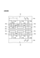
図4に示すB部には、マッハツェンダ型光導波路37dの一方の並行導波路39bを挟んで対向する一方の第2制御電極44と第1制御電極43とが示されている。なお、図3において他方の並行導波路39aを挟んで対向する他方の第2制御電極44と第1制御電極43も、図4に示す構成と同様に構成される。
ここで、補助電極43dおよび44dは、それぞれ、隣接する接続電極43b同士および44d同士を接続し得る任意の位置に配されるものとすることができる。
[第1変形例]
上述した図4に示す第1制御電極43および第2制御電極44では、接続電極43bおよび44bのそれぞれは、セグメント電極43cおよび44cのそれぞれの、並行導波路39の延在方向に沿った長さ方向の中央部分に接続されているものとした。ただし、これは一例であって、接続電極43bおよび44bのそれぞれは、セグメント電極43cおよび44cのそれぞれの任意の位置に接続されているものとすることができる。
上述した図4に示す第1制御電極43および第2制御電極44において、補助電極43dおよび44dの位置は、隣接する接続電極43b同士および44b同士を接続できる限り任意である。ただし、補助電極43dおよび44dは、それぞれ、セグメント電極43cおよび44cに近い位置に配置されるか、共通電極43aおよび44aに近い位置に配置されるかで、それぞれ異なる効果を有する。
光変調素子3の第3の変形例として、補助電極43dは、例えば、セグメント電極43cに対向する辺が、共通電極43aの並行導波路39側の辺とセグメント電極43cの並行導波路39側の辺との距離を二等分する位置よりも共通電極43aに近い位置に配されている。同様に、補助電極44dは、セグメント電極44cに対向する辺が、共通電極44aの並行導波路39側の辺とセグメント電極44cの並行導波路39側の辺との距離を二等分する位置よりも共通電極44aに近い位置に配されている。
光変調素子3の第3の変形例として、補助電極43dは、例えば、セグメント電極43cに対向する辺が、共通電極43aの並行導波路39側の辺とセグメント電極43cの並行導波路39側の辺との距離を二等分する位置に配されている。同様に、補助電極44dは、セグメント電極44cに対向する辺が、共通電極44aの並行導波路39側の辺とセグメント電極44cの並行導波路39側の辺との距離を二等分する位置に配されている。
並行導波路39を挟んで対向する第1制御電極43のセグメント電極43cと第2制御電極44のセグメント電極44cとは、必ずしも図4に示すように並行導波路39に関して線対称に構成されていなくてもよい。
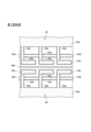
光変調素子3の第6の変形例として、制御電極42と光学基板30との間に、弾性係数が制御電極42の10分の1以下の低弾性材料から成る低弾性層が配されているものとすることができる。低弾性層45を構成する低弾性材料としては、例えば、樹脂を用いることができる。
光変調素子3の第7の変形例として、第6の変形例において示した低弾性層45は、低弾性層45の厚さ方向に延在する一つ又は複数の貫通穴を有し、制御電極42は、上記貫通穴を通って光学基板の主面まで延在するよう構成される。
次に、本発明の第2の実施形態について説明する。本実施形態は、第1の実施形態又はその変形例に係る光変調器1を搭載した光送信装置60である。図16は、本実施形態に係る光送信装置60の構成を示す図である。この光送信装置60は、光変調器1と、光源61と、変調信号生成部62と、を有する。変調信号生成部62は、光変調器1に変調動作を行わせるための高周波信号(変調信号)を生成する電子回路である。変調信号生成部62は、例えば、外部から与えられる送信データに基づき、光変調器1が備える光変調素子3に入力するための4つの変調信号を生成して、光変調器1の信号ピン4に入力する。これにより、光変調器1は、入力光ファイバ6から入射される光源61からの光を変調し、出力光ファイバ7を介して変調光を出力する。
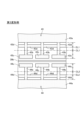
図2に示す構成において、ネスト型マッハツェンダ型光導波路35a、35bの動作点を調整するためのバイアス電極51も、図4に示す制御電極42と同様に構成するものすることができる。図17は、制御電極42と同様に構成されたバイアス電極51の一例を示す図である。図示の例では、ネスト型マッハツェンダ型光導波路35aの一方の並行導波路35a1(図2参照)を挟む2つのバイアス電極51が、それぞれ、第1制御電極43および第2制御電極44と同様に構成されている。
上記の実施形態および変形例は、以下の構成をサポートする。
構成1の光導波路素子によれば、セグメント電極のそれぞれには、接続電極と補助電極とを介して共通電極から電圧が供給されるので、セグメント電極の線幅が狭く一部のセグメント電極において導体欠損が生じても、他のセグメント電極により、光導波路を伝搬する光波を正常に制御することができる。このため、構成1の光導波路素子によれば、セグメント電極を細く形成してバイアス点変動量を低減しつつ、光導波路素子としての製造歩留まりおよび長期信頼性を向上することができる。
構成2の光導波路素子によれば、高周波伝送線路として構成される高周波電極に比べて一般に設計自由度の高いバイアス電極において、電極線幅を狭く構成してバイアス点変動を低減することができる。
構成3の光導波路素子によれば、接続電極における導体欠損の発生を共通電極から補助電極までの範囲に留めつつ当該欠損に対する電気の迂回路を補助電極により確保し得る確率が高まる。したがって、構成3の光導波路素子によれば、光導波路素子としての製造歩留まりおよび長期信頼性を、より向上することができる。
構成4の光導波路素子によれば、補助電極は、共通電極寄りに、セグメント電極から離れて形成されるので、補助電極に起因して光導波路近傍の光学基板に発生し得る基板応力を低減することができる。このため、構成4の光導波路素子によれば、バイアス点変動量をより低減することができる。
構成5の光導波路素子によれば、製造歩留まりおよび長期信頼性の向上効果と、バイアス点変動量の低減効果とを、バランス良く発揮させることができる。
構成6の光導波路素子によれば、光導波路近傍における基板応力を低減してバイアス点変動量を低減することができる。
構成7の光導波路素子によれば、光導波路の近傍における基板応力の発生を更に抑制して、バイアス点変動量を更に低減することができる。
構成8の光導波路素子によれば、制御電極と光学基板との境界部に発生する基板応力を緩和して、さらにバイアス点変動量を低減することができる。
構成9の光変調器によれば、製造歩留まりおよび又は長期信頼性を向上しつつ、駆動電圧のバイアス点変動を低減することができる。
構成10の光送信装置によれば、製造歩留まりおよび又は長期信頼性を向上しつつ駆動電圧のバイアス点変動が低減された光変調器を用いるので、伝送品質の高い光送信装置を安価に実現することができる。
Claims (10)
- 光学基板の主面上に配された光導波路と、前記光導波路を伝搬する光波を制御する制御電極と、を有する光導波路素子であって、
前記制御電極は、前記光学基板の主面上において前記光導波路を挟んで対向する第1制御電極と第2制御電極とを含み、
前記第1制御電極および前記第2制御電極は、それぞれ、前記光導波路に沿って延在する共通電極と、前記共通電極よりも前記光導波路に近接して配された、前記光導波路の延在方向に沿って分割された複数のセグメント電極と、前記複数のセグメント電極のそれぞれを前記共通電極に接続する複数の接続電極と、前記光導波路の延在方向に延びて、隣接する前記接続電極を互いに接続する補助電極と、含む、
光導波路素子。 - 前記光学基板上に配された、前記光導波路を伝搬する光波を変調して変調動作を行うための高周波電極を更に含み、
前記制御電極は、前記変調動作のバイアス点の制御を行うバイアス電極である、
請求項1に記載の光導波路素子。 - 前記補助電極は、前記セグメント電極に対向する辺が、前記共通電極の前光導波路の側の辺と前記セグメント電極の前記光導波路の側の辺との距離を二等分する位置よりも前記セグメント電極に近い位置に配されている、
請求項1または2に記載の光導波路素子。 - 前記補助電極は、前記セグメント電極に対向する辺が、前記共通電極の前光導波路の側の辺と前記セグメント電極の前記光導波路の側の辺との距離を二等分する位置よりも前記共通電極に近い位置に配されている、
請求項1または2に記載の光導波路素子。 - 前記補助電極は、前記セグメント電極に対向する辺が、前記共通電極の前光導波路の側の辺と前記セグメント電極の前記光導波路の側の辺との距離を二等分する位置に配されている、
請求項1または2に記載の光導波路素子。 - 前記セグメント電極の厚みは、3μm以下である、
請求項1ないし5のいずれか一項に記載の光導波路素子。 - 前記光導波路の延在方向に直交する方向に測った前記セグメント電極の幅は、前記補助電極の幅より狭い、
請求項1ないし6のいずれか一項に記載の光導波路素子。 - 前記制御電極と前記光学基板との間に、弾性係数が前記共通電極の10分の1以下の低弾性材料から成る低弾性層が配されている、
請求項1ないし7のいずれか一項に記載の光導波路素子。 - 光変調素子である請求項1ないし8のいずれか一項に記載の光導波路素子と、
前記光導波路素子を収容する筐体と、
前記光導波路素子に光を入力する光ファイバと、
前記光導波路素子が出力する光を前記筐体の外部へ導く光ファイバと、
を備える光変調器。 - 請求項9に記載の光変調器と、
前記光導波路素子に光変調動作を行わせるための電気信号を生成する電子回路と、
を備える光送信装置。
Priority Applications (2)
| Application Number | Priority Date | Filing Date | Title |
|---|---|---|---|
| PCT/JP2022/048045 WO2024142183A1 (ja) | 2022-12-26 | 2022-12-26 | 光導波路素子、光変調器、および光送信装置 |
| CN202280101968.6A CN120225948A (zh) | 2022-12-26 | 2022-12-26 | 光波导元件、光调制器及光发送装置 |
Applications Claiming Priority (1)
| Application Number | Priority Date | Filing Date | Title |
|---|---|---|---|
| PCT/JP2022/048045 WO2024142183A1 (ja) | 2022-12-26 | 2022-12-26 | 光導波路素子、光変調器、および光送信装置 |
Publications (1)
| Publication Number | Publication Date |
|---|---|
| WO2024142183A1 true WO2024142183A1 (ja) | 2024-07-04 |
Family
ID=91716680
Family Applications (1)
| Application Number | Title | Priority Date | Filing Date |
|---|---|---|---|
| PCT/JP2022/048045 Ceased WO2024142183A1 (ja) | 2022-12-26 | 2022-12-26 | 光導波路素子、光変調器、および光送信装置 |
Country Status (2)
| Country | Link |
|---|---|
| CN (1) | CN120225948A (ja) |
| WO (1) | WO2024142183A1 (ja) |
Citations (7)
| Publication number | Priority date | Publication date | Assignee | Title |
|---|---|---|---|---|
| JP2003530592A (ja) * | 2000-04-06 | 2003-10-14 | ブッカム・テクノロジー・ピーエルシー | 予め決められた周波数チャープを有する光変調器 |
| JP2004102160A (ja) * | 2002-09-12 | 2004-04-02 | Fujitsu Quantum Devices Ltd | 光変調器及びその製造方法 |
| JP2006084537A (ja) * | 2004-09-14 | 2006-03-30 | Fujitsu Ltd | 光デバイス |
| WO2006126460A1 (ja) * | 2005-05-23 | 2006-11-30 | Sharp Kabushiki Kaisha | アクティブマトリクス基板、表示装置および画素欠陥修正方法 |
| JP2009098640A (ja) * | 2007-09-12 | 2009-05-07 | Anritsu Corp | 光変調器 |
| JP2013235247A (ja) * | 2012-04-11 | 2013-11-21 | Nippon Telegr & Teleph Corp <Ntt> | 半導体光変調素子 |
| US20210157177A1 (en) * | 2019-11-27 | 2021-05-27 | HyperLight Corporation | Electro-optic devices having engineered electrodes |
-
2022
- 2022-12-26 WO PCT/JP2022/048045 patent/WO2024142183A1/ja not_active Ceased
- 2022-12-26 CN CN202280101968.6A patent/CN120225948A/zh active Pending
Patent Citations (7)
| Publication number | Priority date | Publication date | Assignee | Title |
|---|---|---|---|---|
| JP2003530592A (ja) * | 2000-04-06 | 2003-10-14 | ブッカム・テクノロジー・ピーエルシー | 予め決められた周波数チャープを有する光変調器 |
| JP2004102160A (ja) * | 2002-09-12 | 2004-04-02 | Fujitsu Quantum Devices Ltd | 光変調器及びその製造方法 |
| JP2006084537A (ja) * | 2004-09-14 | 2006-03-30 | Fujitsu Ltd | 光デバイス |
| WO2006126460A1 (ja) * | 2005-05-23 | 2006-11-30 | Sharp Kabushiki Kaisha | アクティブマトリクス基板、表示装置および画素欠陥修正方法 |
| JP2009098640A (ja) * | 2007-09-12 | 2009-05-07 | Anritsu Corp | 光変調器 |
| JP2013235247A (ja) * | 2012-04-11 | 2013-11-21 | Nippon Telegr & Teleph Corp <Ntt> | 半導体光変調素子 |
| US20210157177A1 (en) * | 2019-11-27 | 2021-05-27 | HyperLight Corporation | Electro-optic devices having engineered electrodes |
Also Published As
| Publication number | Publication date |
|---|---|
| CN120225948A (zh) | 2025-06-27 |
Similar Documents
| Publication | Publication Date | Title |
|---|---|---|
| US20240210784A1 (en) | Optical waveguide element, optical modulator, and optical transmission device | |
| CN113050301B (zh) | 光波导元件、光调制器、光调制模块以及光发送装置 | |
| US20230367169A1 (en) | Optical waveguide element, optical modulator, optical modulation module, and optical transmission device | |
| US20230367147A1 (en) | Optical waveguide element, optical modulator, optical modulation module, and optical transmission device | |
| US11442329B2 (en) | Optical waveguide element, optical modulator, optical modulation module, and optical transmission apparatus | |
| US20240319558A1 (en) | Optical waveguide element, optical modulator, optical modulation module, and optical transmission device | |
| US20220381977A1 (en) | Optical waveguide device, manufacturing method of optical modulation element, optical modulator, optical modulation module, and optical transmission apparatus | |
| WO2019167486A1 (ja) | 光変調器、及び光伝送装置 | |
| US11493788B2 (en) | Optical modulator | |
| US20230258967A1 (en) | Optical waveguide device, optical modulator, optical modulation module, and optical transmission apparatus | |
| WO2024142183A1 (ja) | 光導波路素子、光変調器、および光送信装置 | |
| JP7746750B2 (ja) | 光デバイス及び光通信装置 | |
| US20240152021A1 (en) | Optical waveguide element, optical modulator, optical modulation module, and optical transmission device | |
| JP7543879B2 (ja) | 光導波路素子、光変調器、光変調モジュール、及び光送信装置 | |
| EP4603896A1 (en) | Optical modulation device, optical modulator, optical modulation module, optical transmission apparatus, and optical transmission system | |
| US20220291533A1 (en) | Optical modulator and optical transmission apparatus using same | |
| US20250264746A1 (en) | Optical modulation device, optical modulator, optical modulation module, optical transmission apparatus, and optical transmission system | |
| US20250264744A1 (en) | Optical modulation device, optical modulator, optical modulation module, optical transmission apparatus, and optical transmission system |
Legal Events
| Date | Code | Title | Description |
|---|---|---|---|
| 121 | Ep: the epo has been informed by wipo that ep was designated in this application |
Ref document number: 22969977 Country of ref document: EP Kind code of ref document: A1 |
|
| WWE | Wipo information: entry into national phase |
Ref document number: 202280101968.6 Country of ref document: CN |
|
| WWP | Wipo information: published in national office |
Ref document number: 202280101968.6 Country of ref document: CN |
|
| NENP | Non-entry into the national phase |
Ref country code: DE |
|
| 122 | Ep: pct application non-entry in european phase |
Ref document number: 22969977 Country of ref document: EP Kind code of ref document: A1 |
|
| NENP | Non-entry into the national phase |
Ref country code: JP |