WO2024135254A1 - 電波反射装置 - Google Patents
電波反射装置 Download PDFInfo
- Publication number
- WO2024135254A1 WO2024135254A1 PCT/JP2023/042565 JP2023042565W WO2024135254A1 WO 2024135254 A1 WO2024135254 A1 WO 2024135254A1 JP 2023042565 W JP2023042565 W JP 2023042565W WO 2024135254 A1 WO2024135254 A1 WO 2024135254A1
- Authority
- WO
- WIPO (PCT)
- Prior art keywords
- radio wave
- wave reflecting
- reflector
- wave reflector
- elements
- Prior art date
- Legal status (The legal status is an assumption and is not a legal conclusion. Google has not performed a legal analysis and makes no representation as to the accuracy of the status listed.)
- Ceased
Links
Images


Classifications
-
- H—ELECTRICITY
- H01—ELECTRIC ELEMENTS
- H01Q—ANTENNAS, i.e. RADIO AERIALS
- H01Q3/00—Arrangements for changing or varying the orientation or the shape of the directional pattern of the waves radiated from an antenna or antenna system
- H01Q3/44—Arrangements for changing or varying the orientation or the shape of the directional pattern of the waves radiated from an antenna or antenna system varying the electric or magnetic characteristics of reflecting, refracting, or diffracting devices associated with the radiating element
- H01Q3/46—Active lenses or reflecting arrays
-
- H—ELECTRICITY
- H01—ELECTRIC ELEMENTS
- H01Q—ANTENNAS, i.e. RADIO AERIALS
- H01Q15/00—Devices for reflection, refraction, diffraction or polarisation of waves radiated from an antenna, e.g. quasi-optical devices
- H01Q15/14—Reflecting surfaces; Equivalent structures
-
- H—ELECTRICITY
- H01—ELECTRIC ELEMENTS
- H01Q—ANTENNAS, i.e. RADIO AERIALS
- H01Q15/00—Devices for reflection, refraction, diffraction or polarisation of waves radiated from an antenna, e.g. quasi-optical devices
- H01Q15/14—Reflecting surfaces; Equivalent structures
- H01Q15/148—Reflecting surfaces; Equivalent structures with means for varying the reflecting properties
Definitions
- One embodiment of the present invention relates to a radio wave reflection device having a radio wave reflection plate made of liquid crystal material, and a control method thereof.
- a phased array antenna device has the characteristic that, when a high-frequency signal is applied to some or all of the multiple antenna elements, the amplitude and phase of each high-frequency signal can be controlled to control the radiation directivity of the antenna while keeping the antenna orientation fixed in one direction.
- a phased array antenna device has been disclosed that uses a phase shifter that utilizes the phenomenon in which the dielectric constant of liquid crystal changes with applied voltage (see Patent Document 1).
- Patent Document 2 discloses a metasurface that applies a voltage to a radio wave reflecting element that contains liquid crystal, thereby changing the orientation of the liquid crystal molecules in the radio wave reflecting element, adjusting the reflection phase, and controlling the corresponding resonant frequency of the radio wave reflecting element.
- radio wave reflectors It is desirable for radio wave reflectors to be large in order to increase the reflection strength of radio waves. However, from the standpoint of manufacturing, transporting, and installation, the larger they are, the higher the costs in all respects, which is undesirable. Therefore, it is effective to use them in tiling, where multiple radio wave reflectors are installed in combination to increase the size when in use.
- the size of this ineffective area varies depending on the size of the frame and the gaps between the radio wave reflectors. For this reason, when combining radio wave reflectors into one large radio wave reflecting device, there is an issue that the pitch of the radio wave reflecting elements is not constant within the surface, compromising the in-surface uniformity of the radio wave reflecting surface.
- the radio wave reflecting device includes at least a first radio wave reflector and a second radio wave reflector, each of which includes a radio wave reflecting surface on which a plurality of radio wave reflecting elements are arranged, and a mounting section provided along a first edge of the radio wave reflecting surface and on which a circuit for driving the plurality of radio wave reflecting elements is mounted, the second side opposite to the first side on which the mounting section of the first radio wave reflector is arranged so as to overlap the mounting section of the second radio wave reflector, and the normal direction of the radio wave reflecting surface of the first radio wave reflector is inclined with respect to the normal direction of an imaginary line connecting the first side of the first radio wave reflector and the first side of the second radio wave reflector.
- the method for controlling a radio wave reflecting device is as follows: when the first pitch of the multiple radio wave reflecting elements is P and the inclination of the normal direction of the radio wave reflecting surface of the first radio wave reflector relative to the normal direction of the virtual straight line is ⁇ , the amount of phase change ⁇ n of the reflected waves of the first radio wave reflecting element and the nth radio wave reflecting element is 2 ⁇ ((n-1)p sin ⁇ ).
- FIG. 1 is a plan view showing a configuration of a radio wave reflector according to an embodiment of the present invention.
- FIG. 2 is an enlarged plan view showing the configuration of a radio wave reflector according to one embodiment of the present invention.
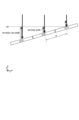
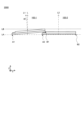
- 1 is a side view showing a configuration of a radio wave reflecting device according to an embodiment of the present invention; 1 is a plan view showing a configuration of a radio wave reflecting device according to an embodiment of the present invention; 1 is an enlarged plan view showing a configuration of a radio wave reflecting device according to an embodiment of the present invention;
- FIG. 11 is a cross-sectional end view showing an example of a thin film transistor of a radio wave reflector according to a modified example of the present invention.
- 1 is an enlarged side view showing a configuration of a radio wave reflector according to an embodiment of the present invention.
- 1 is a side view showing a configuration of a radio wave reflecting device according to an embodiment of the present invention;
- FIG. 1A shows a plan view of a radio wave reflector according to an embodiment of the present invention.
- FIG. 1B shows an enlarged plan view of a reflecting element of the radio wave reflector according to an embodiment of the present invention.
- the radio wave reflector 100 is provided on a first surface of an array substrate 110 with a reflecting area (radio wave reflecting surface) 102 that reflects radio waves and a peripheral area 104 that surrounds the reflecting area 102.
- a plurality of reflecting elements (radio wave reflecting elements) 10 are spaced apart at the same interval w2 as the adjacent reflecting elements 10, and are arranged in an array shape with the same period (pitch) P in a first direction (X direction) parallel to a first side A of the array substrate 110 and a second direction (Y direction) perpendicular to the first direction.
- the reflective element 10 includes a first electrode 150, a liquid crystal layer 130, and a second electrode 170.
- the first electrodes 150 are formed on a first surface of the array substrate 110.
- the second electrodes 170 are formed on a first surface of the counter substrate 120.
- the first electrode 150 and the second electrode 170 are spaced apart and arranged opposite each other in a third direction (Z direction) perpendicular to the first direction (X direction) and the second direction (Y direction).
- the liquid crystal layer 130 is arranged in the area between the first electrode 150 and the second electrode 170.
- the liquid crystal layer 130 and the second electrode 170 are arranged in common to the multiple reflective elements 10.
- the multiple second electrodes 170 are patch electrodes in which adjacent ones are connected to each other by wiring.
- the first electrodes 150 are arranged one by one on the multiple reflective elements 10, and are arranged so that adjacent ones have a gap between them.
- the first electrode 150 is a liquid crystal control electrode that defines one unit of the reflective element 10.
- the radio wave reflector 100 is a device that scatters radio waves incident on its incident surface in a predetermined direction, with the opposing substrate 120 disposed on the incident surface side and the array substrate 110 disposed on the rear side of the incident surface. That is, the second electrode 170 is disposed on the incident surface, and the first electrode 150 is disposed on the rear side of the second electrode 170 with the liquid crystal layer 130 sandwiched therebetween.
- the multiple first electrodes 150 are shown as squares each having the same width w1 in the first direction (X direction) and the second direction (Y direction). However, this is not limited to this, and the multiple first electrodes 150 may have any shape that is symmetrical in the first direction (X direction) and the second direction (Y direction), and may be, for example, polygonal or circular.
- the multiple first electrodes 150 are arranged at equal intervals w2 in a first direction (X-axis direction).
- the multiple first electrodes 150 are arranged at equal intervals w2 in a second direction (Y-axis direction) perpendicular to the first direction.
- the intervals w2 between the multiple first electrodes 150 aligned in the first direction (X-axis direction) are approximately the same as the intervals w2 between the multiple first electrodes 150 aligned in the second direction (Y-axis direction).
- the multiple first electrodes 150 are arranged in an array with the same period (pitch) P in a first direction (X-axis direction).
- the multiple first electrodes 150 are arranged in an array with the same period (pitch) P in a second direction (Y-axis direction) perpendicular to the first direction.
- the period (pitch) P of the multiple first electrodes 150 aligned in the first direction (X-axis direction) is approximately the same as the period (pitch) P of the multiple first electrodes 150 aligned in the second direction (Y-axis direction).
- the period (pitch) P of the first electrodes 150 is the sum of the width w1 of the first electrodes 150 and the spacing w2 of the first electrodes 150.
- the period (pitch) P at which the reflective elements 10 are arranged is preferably in the range of 1/3 to 1/2 of the wavelength of the radio wave to maximize reflected power.
- the period (pitch) P at which the reflective elements 10 are arranged is preferably 3 mm to 6 mm.
- the multiple first electrodes 150 arranged along the second direction (Y-axis direction) are electrically connected by a bias signal line 160.
- the bias signal line 160 is drawn from the first end of the reflective area 102 to the peripheral area 104 and is electrically connected to a drive circuit 180 that drives the reflective element 10 via wiring.
- the drive circuit 180 outputs a bias signal to the bias signal line 160.
- the drive circuit 180 is mounted on a mounting section 106 arranged on the first side A (part of the peripheral area 104) of the array substrate 110.
- the opposing substrate 120 exposes wiring (not shown) on the array substrate 110 and the drive circuit 180 at the mounting section 106.
- the mounting section 106 extends in the first direction (X-direction) along the first end of the reflective area 102 and the first side A of the array substrate 110.
- a flexible printed circuit board is further connected to the drive circuit 180 via a terminal (not shown).
- the multiple first electrodes 150 arranged along the first direction (X-axis direction) are electrically connected by a selection signal line 260.
- the selection signal line 260 is drawn from the first end of the reflective area 102 to the peripheral area 104 and is electrically connected to a drive circuit 280 that drives the reflective element 10 via wiring.
- the drive circuit 280 outputs a selection signal to the selection signal line 260.
- the drive circuit 280 is mounted on a mounting section 106 arranged on the first side A (part of the peripheral area 104) of the array substrate 110.
- the opposing substrate 120 exposes wiring (not shown) and the drive circuit 280 on the array substrate 110 at the mounting section 106.
- a flexible printed circuit board is further connected to the drive circuit 280 via a terminal (not shown).
- the drive circuit 180 and the drive circuit 280 may be arranged in an integrated manner.
- each of the first electrodes 150 is connected to a thin film transistor (TFT) 200.
- the thin film transistor 200 used as a switching element has a gate connected to a selection signal line 260, one of the input/output terminals connected to a bias signal line 160, and the other of the input/output terminals connected to the first electrode 150.
- the switching operation (on/off state) of the thin film transistor 200 is controlled by a selection signal from the selection signal line 260, and a bias signal (bias voltage) is input from the bias signal line 160.
- the first electrodes 150 are individually input with a bias signal by the thin film transistor 200. That is, the first electrodes 150 arranged in a matrix are individually input with a bias signal by the thin film transistor 200.
- a liquid crystal layer 130 is filled between the multiple first electrodes 150 and the second electrodes 170.
- the liquid crystal layer 130 is surrounded and sealed by a seal 140.
- the first surface of the array substrate 110 includes a first side A on which the mounting portion 106 is disposed, a second side B opposite the first side A, a third side C connecting the first side A and the second side B, and a fourth side D opposite the third side C.
- the distance a from the first side A on which the mounting portion 106 is disposed to the multiple reflective elements 10 adjacent to the first side A is greater than the distance b from the second side B to the multiple reflective elements 10 adjacent to the second side B, greater than the distance c from the third side C to the multiple reflective elements 10 adjacent to the third side C, and greater than the distance d from the fourth side D to the multiple reflective elements 10 adjacent to the fourth side D.
- the sum of the distance c from the third side C to the multiple reflective elements 10 adjacent to the third side C and the distance d from the fourth side D to the multiple reflective elements 10 adjacent to the fourth side D may be the sum of an integer multiple of the period (pitch) P at which the multiple reflective elements 10 are arranged and the interval w2 between the adjacent reflective elements 10.
- the sum of the width c of the peripheral region arranged on the third side C and the width d of the peripheral region arranged on the fourth side D may satisfy lW1+(l+1)W2 (l is an integer equal to or greater than 0), where W1 is the width of the reflective element 10 and W2 is the interval between the reflective elements 10.
- the width c of the peripheral region indicates the distance between the third side C and the reflective element 10 at the very end of the reflective region 102 in the first direction (X-axis direction)
- the width d of the peripheral region indicates the distance between the fourth side D and the reflective element 10 at the very end of the reflective region 102 in the first direction (X-axis direction).
- twice the distance c from the third side C to the multiple reflective elements 10 adjacent to the third side C may be the sum of an integer multiple of the period (pitch) P at which the multiple reflective elements 10 are arranged and the spacing w2 between adjacent reflective elements 10.
- twice the width c of the peripheral region arranged on the third side C may satisfy mW1+(m+1)W2 (m is an integer equal to or greater than 0), where W1 is the width of the reflective element 10 and W2 is the spacing between the reflective elements 10.
- twice the distance d from the fourth side D to the multiple reflective elements 10 adjacent to the fourth side D may be the sum of an integer multiple of the period (pitch) P at which the multiple reflective elements 10 are arranged and the spacing w2 between adjacent reflective elements 10.
- twice the width d of the peripheral region arranged on the fourth side D may satisfy nW1+(n+1)W2 (n is an integer equal to or greater than 0), where W1 is the width of the reflective element 10 and W2 is the spacing between the reflective elements 10.
- the width c of the peripheral region arranged on the third side C and the distance d from the fourth side D to the multiple reflective elements 10 adjacent to the fourth side D may be different or the same.
- the radio wave reflector according to this embodiment has the above-described configuration, so that when multiple radio wave reflectors are combined, the pitch of the reflecting elements in the first direction (X-axis direction) can be made constant within the plane.
- FIG. 2 shows a side view of a radio wave reflecting device according to an embodiment of the present invention.
- FIG. 3(A) shows a plan view of a radio wave reflecting device according to an embodiment of the present invention.
- FIG. 3(B) shows an enlarged plan view of the connection portion of each radio wave reflecting plate in a radio wave reflecting device according to an embodiment of the present invention.
- the reflecting element 10 shown by the dotted line is not actually arranged, but is shown here as a virtual reflecting element to make it easier to understand the combination pitch.
- the radio wave reflecting device 1000 includes a radio wave reflecting plate 100-1, a radio wave reflecting plate 100-2, a radio wave reflecting plate 100-3, and a radio wave reflecting plate 100-4 (here, when the radio wave reflecting plates 100-1, 100-2, 100-3, and 100-4 are not distinguished from one another, they are referred to as radio wave reflecting plate 100).
- Each of the radio wave reflecting plates 100-1, 100-2, 100-3, and 100-4 has a reflective area 102-1, 102-2, 102-3, and 102-4 that reflects radio waves, and a peripheral area 104-1, 104-2, 104-3, and 104-4 that surrounds the reflective areas 102-1, 102-2, 102-3, and 102-4 (when the reflective areas 102-1, 102-2, 102-3, and 102-4 are not distinguished, they are referred to as reflective area 102, and when the peripheral areas 104-1, 104-2, 104-3, and 104-4 are not distinguished, they are referred to as peripheral area 104).
- the radio wave reflecting plates 100-1, 100-2, 100-3, and 100-4 are arranged so that the reflection areas 102-1, 102-2, 102-3, and 102-4 face the same side.
- a plurality of reflection elements 10 are spaced apart at the same interval w2 as adjacent reflection elements 10, and are arranged in an array with the same period (pitch) P in a first direction (X direction) along a first side A of the array substrate 110 and in a second direction (Y direction) perpendicular to the first direction.
- the first surface of the array substrate 110 of the radio wave reflector 100-1 includes a first side A1 on which the mounting section 106-1 is located, a second side B1 opposite the first side A1, a third side C1 connecting the first side A1 and the second side B1, and a fourth side D1 opposite the third side C1.
- the first surface of the array substrate 110 of the radio wave reflector 100-2 includes a first side A2 on which the mounting section 106-2 is located, a second side B2 opposite the first side A2, a third side C2 connecting the first side A2 and the second side B2, and a fourth side D2 opposite the third side C2.
- the first surface of the array substrate 110 of the radio wave reflector 100-3 includes a first side A3 on which the mounting section 106-3 is located, a second side B3 opposite the first side A3, a third side C3 connecting the first side A3 and the second side B3, and a fourth side D3 opposite the third side C3.
- the first surface of the array substrate 110 of the radio wave reflector 100-4 includes a first side A4 on which the mounting section 106-4 is located, a second side B4 opposite the first side A4, a third side C4 connecting the first side A4 and the second side B4, and a fourth side D4 opposite the third side C4.
- the second side B1 of the radio wave reflector 100-1 and the first side A2 of the radio wave reflector 100-2 are arranged to overlap.
- the second side B1 of the radio wave reflector 100-1 is arranged so as to overlap the mounting section 106-2 arranged on the first side A2 of the radio wave reflector 100-2.
- a spacer 20 is disposed under the second side B2 of the radio wave reflector 100-2.
- the height of the spacer 20 in the normal direction L2 of the reflection area 102-2 may be approximately the same as the height of the mounting portion 106-2 in the normal direction L2 of the reflection area 102-2.
- the reflection position of the first reflection element 10-1 disposed on the second side B1 side of the reflection area 102-1 of the radio wave reflector 100-1 and the reflection position of the first reflection element 10-1 disposed on the second side B2 side of the reflection area 102-2 of the radio wave reflector 100-2 are located at approximately the same height.
- An imaginary straight line LB (dotted line) connecting the reflection position of the first reflection element 10-1 arranged on the second side B1 of the reflection area 102-1 of the radio wave reflector 100-1 and the reflection position of the first reflection element 10-1 arranged on the second side B2 of the reflection area 102-2 of the radio wave reflector 100-2 is arranged approximately parallel to an imaginary straight line LA (two-dot chain line) connecting the first side A1 of the radio wave reflector 100-1 and the first side A2 of the radio wave reflector 100-2.
- LA two-dot chain line
- the normal direction L1 of the reflection area 102-1 of the radio wave reflector 100-1 is inclined with respect to the normal direction L of the imaginary straight line LA connecting the first side A1 of the radio wave reflector 100-1 and the first side A2 of the radio wave reflector 100-2.
- the normal direction L2 of the reflection area 102-2 of the radio wave reflector 100-2 is inclined with respect to the normal direction L of the imaginary straight line LA. It is preferable that the angle ⁇ 1 of the normal direction L1 of the reflection area 102-1 of the radio wave reflector 100-1 with respect to the normal direction L of the imaginary straight line LA and the angle ⁇ 2 of the normal direction L2 of the reflection area 102-2 of the radio wave reflector 100-2 with respect to the normal direction L of the imaginary straight line LA are substantially the same (when there is no need to distinguish between the angles ⁇ 1 and ⁇ 2, the angle is referred to as angle ⁇ ).
- the second side B1 of the radio wave reflector 100-1 and the first side A2 of the radio wave reflector 100-2 are arranged approximately parallel to each other.
- the distance in the second direction (Y-axis direction) between the reflecting element 10 arranged adjacent to the second side B1 of the radio wave reflector 100-1 and the reflecting element 10 arranged adjacent to the first side A2 of the radio wave reflector 100-2 is the sum of an integer multiple of the period (pitch) P at which the multiple reflecting elements 10 are arranged and the interval w2 between the adjacent reflecting elements 10.
- the distance between the reflecting area 102-1 of the radio wave reflector 100-1 and the reflecting area 102-2 of the radio wave reflector 100-2 satisfies oW1+(o+1)W2 (o is an integer equal to or greater than 0), where W1 is the width of the reflecting element 10 and W2 is the interval between the reflecting elements 10.
- the distance between reflection area 102-1 and reflection area 102-2 refers to the distance when viewed in a plan view from the normal direction of reflection area 102-1 and reflection area 102-2, and does not include the distance in the step direction where radio wave reflector 100-1 and radio wave reflector 100-2 overlap.
- the radio wave reflecting device has the above-mentioned configuration, so that when multiple radio wave reflecting plates are combined, the pitch of the reflecting elements in the second direction (Y-axis direction) can be made constant within the plane.
- the third side C1 of the radio wave reflector 100-1 and the third side C2 of the radio wave reflector 100-2 are aligned on the same line in the second direction (Y direction).
- the third side C1 of the radio wave reflector 100-1 and the third side C2 of the radio wave reflector 100-2 may be offset in the first direction (X direction).
- the second side B3 of the radio wave reflector 100-3 and the first side A4 of the radio wave reflector 100-4 are arranged to overlap.
- the second side B3 of the radio wave reflector 100-3 is arranged so as to overlap the mounting portion 106-4 arranged on the first side A4 of the radio wave reflector 100-4.
- radio wave reflector 100-3 and radio wave reflector 100-4 are omitted here as it is the same as that of radio wave reflector 100-1 and radio wave reflector 100-2.
- An imaginary straight line LA connecting the first side A3 of radio wave reflector 100-3 and the first side A4 of radio wave reflector 100-4 is arranged so as to be parallel to an imaginary straight line LA connecting the first side A1 of radio wave reflector 100-1 and the first side A2 of radio wave reflector 100-2. Therefore, the reflection area 102-1 of radio wave reflector 100-1, the reflection area 102-2 of radio wave reflector 100-2, the reflection area 102-3 of radio wave reflector 100-3, and the reflection area 102-4 of radio wave reflector 100-4 are arranged approximately parallel.
- the reflection area 102-1 of the radio wave reflector 100-1, the reflection area 102-2 of the radio wave reflector 100-2, the reflection area 102-3 of the radio wave reflector 100-3, and the reflection area 102-4 of the radio wave reflector 100-4 are arranged approximately parallel to each other, which makes it easy to adjust the position when installing them and simplifies the directional control of the radio waves.
- the third side C1 of the radio wave reflector 100-1 and the fourth side D3 of the radio wave reflector 100-3 are disposed adjacent to each other.
- the third side C1 of the radio wave reflector 100-1 and the fourth side D3 of the radio wave reflector 100-3 are disposed approximately parallel to each other.
- the distance in the first direction (X-axis direction) between the reflecting element 10 arranged adjacent to the third side C1 of the radio wave reflecting plate 100-1 and the reflecting element 10 arranged adjacent to the fourth side D3 of the radio wave reflecting plate 100-3 is the sum of an integer multiple of the period (pitch) P at which the multiple reflecting elements 10 are arranged and the spacing w2 between adjacent reflecting elements 10.
- the distance between the reflecting area 102-1 of the radio wave reflecting plate 100-1 and the reflecting area 102-3 of the radio wave reflecting plate 100-3 satisfies pW1+(p+1)W2 (p is an integer equal to or greater than 0), where W1 is the width of the reflecting element 10 and W2 is the spacing between the reflecting elements 10.
- the distance between the reflective area 102-1 and the reflective area 102-3 refers to the sum of the distance between the third side C1 and the reflective area 102-1 in the first direction (X-axis direction), the distance between the third side C1 and the fourth side D3 in the first direction (X-axis direction), and the distance between the fourth side D3 and the reflective area 102-3 in the first direction (X-axis direction) when viewed in a plane from the normal direction of the reflective area 102-1 and the reflective area 102-3.
- the distance between the reflection area 102-1 of the radio wave reflector 100-1 and the reflection area 102-3 of the radio wave reflector 100-3 is approximately the same as the distance between the reflection area 102-1 of the radio wave reflector 100-1 and the reflection area 102-2 of the radio wave reflector 100-2. Therefore, it is preferable that the integer n and the integer m are the same.
- the third side C1 of the radio wave reflector 100-1 and the fourth side D3 of the radio wave reflector 100-3 are preferably arranged in contact with each other, and the distance between the third side C1 and the fourth side D3 in the first direction (X-axis direction) is preferably 0.
- this is not limited to this, and the reflection area 102-1 of the radio wave reflector 100-1 and the reflection area 102-3 of the radio wave reflector 100-3 may be spaced apart as long as the distance between them satisfies the above range.
- the radio wave reflecting device has the above-mentioned configuration, so that the pitch of the reflecting elements can be made constant within the surface when multiple radio wave reflectors are combined.
- the second side B1 of the radio wave reflector 100-1 and the second side B3 of the radio wave reflector 100-3 are aligned on the same line in the first direction (X direction).
- the second side B1 of the radio wave reflector 100-1 and the second side B3 of the radio wave reflector 100-3 may be offset in the second direction (Y direction).
- the third side C2 of the radio wave reflector 100-2 and the fourth side D4 of the radio wave reflector 100-4 are disposed adjacent to each other.
- the third side C2 of the radio wave reflector 100-2 and the fourth side D4 of the radio wave reflector 100-4 are disposed substantially parallel to each other.
- the arrangement of the radio wave reflector 100-2 and the radio wave reflector 100-4 is the same as the arrangement of the radio wave reflector 100-1 and the radio wave reflector 100-3, so it will not be described here.
- radio wave reflectors 100 In FIG. 3, a configuration in which four radio wave reflectors 100 are combined is shown. However, this is not limited to this, and additional radio wave reflectors 100 may be combined in the lower left and right directions using the radio wave reflectors 100-2 and 100-4 on which the spacers 20 are arranged as a base.
- the second side B of the additional radio wave reflector 100 may be arranged so as to overlap the mounting parts 106-1 and 106-3 of the radio wave reflectors 100-1 and 100-3, the fourth side D of the additional radio wave reflector 100 may be arranged adjacent to the third sides C3 and C4 of the radio wave reflectors 100-3 and 100-4, and the third side C of the additional radio wave reflector 100 may be arranged adjacent to the fourth sides D1 and D2 of the radio wave reflectors 100-1 and 100-2.
- the radio wave reflecting device of this embodiment can reduce the ineffective area where no radio wave reflecting elements are arranged within a surface formed by combining multiple radio wave reflecting plates, and can make the pitch of the reflecting elements constant.
- the radio wave reflecting device of this embodiment can easily adjust its position when installed, and can simplify the directional control of radio waves.
- each first electrode 150 is connected to the bias signal line 160 and the selection signal line 260 via the thin film transistor 200 shown in FIG. 4.
- FIG. 4 is a cross-sectional view showing an example of the thin film transistor 200.
- the thin film transistor 200 has a structure in which, for example, an undercoat layer 1510, a gate electrode 1530, a bottom gate insulating film 1550, an oxide semiconductor layer 1570, a first connection wiring layer 1590, a top gate insulating film 1610, a bottom gate electrode 1630, a passivation film 1650, a second connection wiring layer 1670, a signal line 1690, and an insulating film 1710 are sequentially stacked on the array substrate 110.
- an overcoat layer 1730, an insulating film 1750, a first electrode 150, a first alignment film 112a, a liquid crystal layer 130, a second alignment film 112b, a second electrode 170, and an opposing substrate 120 are sequentially stacked.
- the undercoat layer 1510 may be made of, for example, a silicon oxide film.
- the bottom gate insulating film 1550 may be made of, for example, a laminated structure of a silicon nitride film and a silicon oxide film.
- the gate electrode 1530 may be made of, for example, molybdenum, tungsten, or an alloy thereof.
- the top gate insulating film 1610 may be made of, for example, a silicon oxide film.
- the first connection wiring layer 1590 and the second connection wiring layer 1670 may be made of, for example, a Ti/Al/Ti laminated structure or a Mo/Al/Mo laminated structure.
- the passivation film 1650 may be made of, for example, a silicon nitride film.
- the insulating film 1710 may be made of, for example, a silicon oxide film or a silicon nitride film.
- the first electrode 150 may be made of, for example, a Ti/Al/Ti laminated structure or a Mo/Al/Mo laminated structure.
- the second electrode 170 may be made of, for example, molybdenum, tungsten, or an alloy thereof.
- the thin-film transistor 200 is shown as a dual-gate TFT using an oxide semiconductor, but amorphous silicon or low-temperature polysilicon (LTPS) may also be used. Also, in FIG. 4, an example of vertical electric field driving is shown, but horizontal electric field driving may also be used.
- LTPS low-temperature polysilicon
- the radio wave reflecting device 1000 further includes a control unit (not shown) that controls the potential difference between each of the first electrodes 150 and the second electrode 170 via each thin film transistor 200.
- the control unit controls the voltage applied to each of the first electrodes 150 to control the potential difference between each of the first electrodes 150 and the second electrode 170, and drives each liquid crystal layer 130 to change the dielectric constant of the liquid crystal molecules in their orientation state.
- the phase of the radio wave reflected by each reflecting element 10 changes, and as a result, the traveling direction of the irradiated radio wave changes. This mechanism allows the radio wave reflector 100 to reflect radio waves at a reflection angle different from the angle of incidence.
- the normal direction of the reflection area 102 of the radio wave reflector 100 is inclined at an angle ⁇ in the second direction (Y-axis direction) with respect to the normal direction L of the virtual straight line LA. Therefore, the reflection angle of the multiple reflection elements 10 arranged in the second direction (Y-axis direction) needs to be corrected by the inclination angle ⁇ of the radio wave reflector 100.
- the reflection angle is determined by the amount of change in the phase of the reflected wave, and the amount of change in the phase of the reflected wave can be controlled by controlling the potential difference between the first electrode 150 and the second electrode 170 by the control unit.
- each first electrode 150 is connected to a selection signal line 260 via a thin film transistor 200 shown in FIG. 4 and is controlled individually.
- the multiple reflective elements 10 arranged in the second direction have different phases of reflected waves.
- the multiple reflective elements 10 arranged in the second direction delay the phase of the reflected wave from the second side B side to the first side A side of the array substrate 110.
- the multiple reflective elements 10 of the radio wave reflector 100 include a first reflective element 10-1, a second reflective element 10-2 adjacent to the first side A side of the first reflective element 10-1, and an nth reflective element 10-n arranged on the first side A side of the first reflective element 10-1 with n-2 reflective elements 10 in between.
- the phase change amount ⁇ 2 of the reflected wave of the second reflecting element 10-2 based on the reflection position LB of the first reflecting element 10-1 satisfies 2 ⁇ (p sin ⁇ )
- the phase change amount ⁇ n of the reflected wave of the nth reflecting element 10-n based on the reflection position LB of the first reflecting element 10-1 satisfies 2 ⁇ ((n-1)p sin ⁇ ).
- the nth reflecting element 10-n has a phase delay of 2 ⁇ ((n-1)p ⁇ sin ⁇ ) relative to the first reflecting element 10-1, so a voltage that advances the phase by that amount is applied to the nth reflecting element 10-n. If the applied voltage to the first reflecting element 10-1 is Vpp and the wavelength of the radio wave is ⁇ , the applied voltage V2 to the second reflecting element 10-2 satisfies Vpp ⁇ 2/ ⁇ , and the applied voltage Vn to the nth reflecting element 10-n satisfies Vpp ⁇ n/ ⁇ .
- the phase of the reflected waves of the multiple reflecting elements 10 of the radio wave reflector 100 can be aligned to the reflection position LB of the first reflecting element 10-1. It is preferable that the applied voltage Vn to the nth reflecting element 10-n is appropriately adjusted based on the gamma characteristics of the liquid crystal.
- the reflection areas 102 of the multiple radio wave reflectors 100 are arranged approximately parallel, so by making the same correction to each reflection element 10 in all the radio wave reflectors 100, the phases of the reflected waves of the multiple radio wave reflectors 100 in the radio wave reflecting device 1000 can be aligned.
- the radio wave reflector 100 has a reflection axis parallel to the first direction (X-axis direction) and a reflection axis parallel to the second direction (Y-axis direction).
- each first electrode 150 is connected to a bias signal line 160 and a selection signal line 260 via a thin film transistor 200 shown in FIG. 4, and is individually controlled. Therefore, the radio wave reflector 100 can control the reflection angle in the rotation direction about the reflection axis parallel to the first direction (X-axis direction) and the reflection axis parallel to the second direction (Y-axis direction). Therefore, by combining these, it becomes possible to control the reflection angle in all directions forward for the radio wave reflecting device 1000.
- the radio wave reflecting device 2000 of the second embodiment is the same as the radio wave reflecting device 1000 of the first embodiment, except that, as shown in FIG. 6, the spacer 20 is not arranged under the second sides B2 and B4 of the radio wave reflecting plates 100-2 and 100-4. Therefore, a repeated explanation will be omitted.
- the normal direction L2 of the reflection area 102-2 of the radio wave reflector 100-2 is approximately parallel to the normal direction L of the imaginary straight line LA connecting the first side A1 of the radio wave reflector 100-1 and the first side A2 of the radio wave reflector 100-2.
- the normal direction of the reflection area 102-4 of the radio wave reflector 100-4 (not shown) is approximately parallel to the normal direction L of the imaginary straight line LA connecting the first side A1 of the radio wave reflector 100-1 and the first side A2 of the radio wave reflector 100-2. Therefore, in the radio wave reflectors 100-2 and 100-4, it is not necessary to correct the reflection angle for the multiple reflecting elements 10 arranged in the second direction (Y-axis direction).
- the reflection position LB of the first reflecting element 10-1 arranged on the second side B1 of the reflection area 102-1 of the radio wave reflector 100-1 is different from the reflection position of the first reflecting element 10-1 arranged on the second side B2 of the reflection area 102-2 of the radio wave reflector 100-2.
- the reflection position of the nth reflecting element 10-n arranged on the first side A1 of the reflection area 102-1 of the radio wave reflector 100-1 and the reflection position of the first reflecting element 10-1 arranged on the second side B2 of the reflection area 102-2 of the radio wave reflector 100-2 are located at approximately the same height.
- the radio wave reflectors 100-2 and 100-4 it is necessary to correct the reflection positions of the multiple reflecting elements 10 arranged in the second direction (Y-axis direction).
- the period (pitch) of the multiple reflecting elements 10 aligned in the second direction (Y-axis direction) is P
- the inclination of the normal direction L1 of the reflecting area 102-1 of the radio wave reflecting plate 100-1 relative to the normal direction L of the virtual straight line LA is ⁇ 1
- the reflecting element 10 arranged in the reflection area 102-2 of the radio wave reflector 100-2 has a phase delay of 2 ⁇ ((n-1)p sin ⁇ ) relative to the first reflecting element 10-1 arranged on the second side B1 of the reflection area 102-1 of the radio wave reflector 100-1, so a voltage that advances the phase by that amount is applied to the reflecting element 10 arranged in the reflection area 102-2 of the radio wave reflector 100-2.
- the applied voltage of the first reflecting element 10-1 arranged on the second side B1 of the reflection area 102-1 of the radio wave reflector 100-1 is Vpp and the wavelength of the radio waves is ⁇
- the applied voltage Vn of the reflecting element 10 arranged in the reflection area 102-2 of the radio wave reflector 100-2 satisfies Vpp ⁇ n/ ⁇ .
- the phase of the reflected waves of the multiple reflecting elements 10 of the radio wave reflector 100-2 can be aligned with the reflection position LB of the first reflecting element 10-1 of the reflecting area 102-1 of the radio wave reflector 100-1.
- the reflection areas 102 of the multiple radio wave reflectors 100 other than the radio wave reflectors 100-2 and 100-4, which do not have spacers 20, are arranged approximately parallel, so by making a similar correction to each reflection element 10 in these radio wave reflectors 100, the phases of the reflected waves of the multiple radio wave reflectors 100 in the radio wave reflecting device 2000 can be aligned.
Landscapes
- Physics & Mathematics (AREA)
- Electromagnetism (AREA)
- Aerials With Secondary Devices (AREA)
Priority Applications (2)
| Application Number | Priority Date | Filing Date | Title |
|---|---|---|---|
| JP2024565711A JPWO2024135254A1 (https=) | 2022-12-22 | 2023-11-28 | |
| US19/243,985 US20250316910A1 (en) | 2022-12-22 | 2025-06-20 | Reflecting device and control method thereof |
Applications Claiming Priority (2)
| Application Number | Priority Date | Filing Date | Title |
|---|---|---|---|
| JP2022-205319 | 2022-12-22 | ||
| JP2022205319 | 2022-12-22 |
Related Child Applications (1)
| Application Number | Title | Priority Date | Filing Date |
|---|---|---|---|
| US19/243,985 Continuation US20250316910A1 (en) | 2022-12-22 | 2025-06-20 | Reflecting device and control method thereof |
Publications (1)
| Publication Number | Publication Date |
|---|---|
| WO2024135254A1 true WO2024135254A1 (ja) | 2024-06-27 |
Family
ID=91588184
Family Applications (1)
| Application Number | Title | Priority Date | Filing Date |
|---|---|---|---|
| PCT/JP2023/042565 Ceased WO2024135254A1 (ja) | 2022-12-22 | 2023-11-28 | 電波反射装置 |
Country Status (3)
| Country | Link |
|---|---|
| US (1) | US20250316910A1 (https=) |
| JP (1) | JPWO2024135254A1 (https=) |
| WO (1) | WO2024135254A1 (https=) |
Citations (3)
| Publication number | Priority date | Publication date | Assignee | Title |
|---|---|---|---|---|
| JP2019530387A (ja) * | 2016-09-22 | 2019-10-17 | 華為技術有限公司Huawei Technologies Co.,Ltd. | ビーム・ステアリング・アンテナのための液晶調整可能メタサーフェス |
| JP2021175054A (ja) * | 2020-04-22 | 2021-11-01 | Kddi株式会社 | メタサーフェス反射板アレイ |
| WO2022244676A1 (ja) * | 2021-05-17 | 2022-11-24 | 株式会社ジャパンディスプレイ | 電波反射板および電波反射装置 |
-
2023
- 2023-11-28 WO PCT/JP2023/042565 patent/WO2024135254A1/ja not_active Ceased
- 2023-11-28 JP JP2024565711A patent/JPWO2024135254A1/ja active Pending
-
2025
- 2025-06-20 US US19/243,985 patent/US20250316910A1/en active Pending
Patent Citations (3)
| Publication number | Priority date | Publication date | Assignee | Title |
|---|---|---|---|---|
| JP2019530387A (ja) * | 2016-09-22 | 2019-10-17 | 華為技術有限公司Huawei Technologies Co.,Ltd. | ビーム・ステアリング・アンテナのための液晶調整可能メタサーフェス |
| JP2021175054A (ja) * | 2020-04-22 | 2021-11-01 | Kddi株式会社 | メタサーフェス反射板アレイ |
| WO2022244676A1 (ja) * | 2021-05-17 | 2022-11-24 | 株式会社ジャパンディスプレイ | 電波反射板および電波反射装置 |
Also Published As
| Publication number | Publication date |
|---|---|
| JPWO2024135254A1 (https=) | 2024-06-27 |
| US20250316910A1 (en) | 2025-10-09 |
Similar Documents
| Publication | Publication Date | Title |
|---|---|---|
| JP7743514B2 (ja) | 電波反射板 | |
| WO2022244676A1 (ja) | 電波反射板および電波反射装置 | |
| JP7500323B2 (ja) | フェーズドアレイアンテナの駆動方法及び反射板の駆動方法 | |
| JP7589093B2 (ja) | 電波反射板 | |
| JP7711168B2 (ja) | 電波反射板 | |
| JP7589092B2 (ja) | 電波反射板 | |
| WO2022259789A1 (ja) | 電波反射板及びフェーズドアレイアンテナ | |
| US20250015508A1 (en) | Reflect array | |
| US20240364008A1 (en) | Reflect array | |
| WO2023058399A1 (ja) | 電波反射装置 | |
| US20250149800A1 (en) | Reflecting device | |
| WO2024135254A1 (ja) | 電波反射装置 | |
| WO2024116573A1 (ja) | 電波反射装置 | |
| WO2025169782A1 (ja) | 電波反射装置の調整方法 | |
| US20250379366A1 (en) | Intelligent reflecting surface and reflecting device | |
| US20250266865A1 (en) | Intelligent reflecting surface | |
| US20260005436A1 (en) | Reflecting element for intelligent reflecting surface | |
| US20250226588A1 (en) | Intelligent reflecting surface | |
| WO2024185259A1 (ja) | 電波反射装置 | |
| US20260003234A1 (en) | Intelligent reflecting surface | |
| WO2025027981A1 (ja) | 電波反射装置の検査装置、およびその検査方法 | |
| US20250093708A1 (en) | Reflecting device | |
| US20250379617A1 (en) | Intelligent reflecting surface | |
| WO2024202471A1 (ja) | 電波反射装置 | |
| WO2026023255A1 (ja) | 電波反射装置 |
Legal Events
| Date | Code | Title | Description |
|---|---|---|---|
| 121 | Ep: the epo has been informed by wipo that ep was designated in this application |
Ref document number: 23906622 Country of ref document: EP Kind code of ref document: A1 |
|
| WWE | Wipo information: entry into national phase |
Ref document number: 2024565711 Country of ref document: JP |
|
| NENP | Non-entry into the national phase |
Ref country code: DE |
|
| 122 | Ep: pct application non-entry in european phase |
Ref document number: 23906622 Country of ref document: EP Kind code of ref document: A1 |