WO2024128094A1 - 表示制御装置、それを用いた自動車、表示システム - Google Patents
表示制御装置、それを用いた自動車、表示システム Download PDFInfo
- Publication number
- WO2024128094A1 WO2024128094A1 PCT/JP2023/043658 JP2023043658W WO2024128094A1 WO 2024128094 A1 WO2024128094 A1 WO 2024128094A1 JP 2023043658 W JP2023043658 W JP 2023043658W WO 2024128094 A1 WO2024128094 A1 WO 2024128094A1
- Authority
- WO
- WIPO (PCT)
- Prior art keywords
- display
- display device
- video data
- image
- osd
- Prior art date
- Legal status (The legal status is an assumption and is not a legal conclusion. Google has not performed a legal analysis and makes no representation as to the accuracy of the status listed.)
- Ceased
Links
Images


Classifications
-
- B—PERFORMING OPERATIONS; TRANSPORTING
- B60—VEHICLES IN GENERAL
- B60K—ARRANGEMENT OR MOUNTING OF PROPULSION UNITS OR OF TRANSMISSIONS IN VEHICLES; ARRANGEMENT OR MOUNTING OF PLURAL DIVERSE PRIME-MOVERS IN VEHICLES; AUXILIARY DRIVES FOR VEHICLES; INSTRUMENTATION OR DASHBOARDS FOR VEHICLES; ARRANGEMENTS IN CONNECTION WITH COOLING, AIR INTAKE, GAS EXHAUST OR FUEL SUPPLY OF PROPULSION UNITS IN VEHICLES
- B60K35/00—Instruments specially adapted for vehicles; Arrangement of instruments in or on vehicles
-
- G—PHYSICS
- G09—EDUCATION; CRYPTOGRAPHY; DISPLAY; ADVERTISING; SEALS
- G09G—ARRANGEMENTS OR CIRCUITS FOR CONTROL OF INDICATING DEVICES USING STATIC MEANS TO PRESENT VARIABLE INFORMATION
- G09G5/00—Control arrangements or circuits for visual indicators common to cathode-ray tube indicators and other visual indicators
- G09G5/36—Control arrangements or circuits for visual indicators common to cathode-ray tube indicators and other visual indicators characterised by the display of a graphic pattern, e.g. using an all-points-addressable [APA] memory
- G09G5/37—Details of the operation on graphic patterns
- G09G5/377—Details of the operation on graphic patterns for mixing or overlaying two or more graphic patterns
-
- H—ELECTRICITY
- H04—ELECTRIC COMMUNICATION TECHNIQUE
- H04N—PICTORIAL COMMUNICATION, e.g. TELEVISION
- H04N5/00—Details of television systems
- H04N5/66—Transforming electric information into light information
Definitions
- This disclosure relates to a display control device, an automobile using the same, and a display system.
- Patent Document 1 discloses a technology that provides an OSD function to an in-vehicle display device.
- the display on the display device may transition from the normal image to a black image, etc. During this transition, the entire screen may not become a black image, and the normal image may be partially displayed, resulting in an image not being displayed properly on the display device.
- This disclosure has been made in light of these circumstances, and one of its illustrative purposes is to provide a technique for appropriately displaying images when transitioning displays on a display device with an OSD function.
- the display control device includes an output interface that outputs video data and image data for OSD (On Screen Display) to be superimposed on the video data to a display device, and an acquisition unit that acquires mask data for masking the display of the display device.
- OSD On Screen Display
- the output interface When switching the video data to be output to the display device, the output interface outputs the mask data to the display device so that the display of the display device is masked when the display transitions in response to the switching of the video data.
- the display system includes the display control device and a display device.
- the display on the display device is masked based on the mask data when a transition occurs in response to switching of video data.
- a display control device includes an output interface that outputs video data and image data for OSD (On Screen Display) to be superimposed on the video data to a display device, and a generation unit that generates a synchronization signal for the video data output from the output interface.
- OSD On Screen Display
- the output interface When switching the video data to be output to the display device, the output interface outputs the synchronization signal for the video data before the switch to the display device together with the video data after the switch.
- a display system includes the above-mentioned display control device and a display device.
- the display device displays an image corresponding to the switched video data based on a synchronization signal of the video data before the switch.
- Another aspect of the present disclosure is an automobile.
- the automobile is equipped with the above-described display system.
- This disclosure provides a technique for appropriately displaying images when transitioning displays on a display device that uses an OSD function.
- FIG. 1 is a block diagram showing the configuration of a display system according to the first embodiment.
- FIG. 2 is a block diagram for explaining details of the timing controller according to the first embodiment.
- FIG. 3A is a diagram showing an example of an image normally displayed on the display device.
- FIG. 3B is a diagram showing an example of an image displayed during a display transition on the display device.
- FIG. 3C is a diagram showing an example of an image displayed on the display device after the transition.
- FIG. 4A is a diagram showing an example of an image normally displayed on the display device.
- FIG. 4B shows the image displayed during the transition.
- FIG. 4C is a diagram showing an example of an image displayed on the display device after the transition.
- FIG. 4A is a diagram showing an example of an image normally displayed on the display device.
- FIG. 4B shows the image displayed during the transition.
- FIG. 4C is a diagram showing an example of an image displayed on the display device after the transition.
- FIG. 5 is a flowchart for explaining an example of the operation of the display system according to the first embodiment.
- FIG. 6A shows an image displayed on a display panel before a transition.
- FIG. 6B is a diagram showing the image to be displayed on the display panel after the transition.
- FIG. 6C illustrates an image that may be displayed on a display panel during the transition.
- FIG. 7 is a block diagram for explaining details of the timing controller according to the second embodiment.
- FIG. 8A is a diagram showing an example of an image normally displayed on the display device.
- FIG. 8B is a diagram showing an example of an image displayed on the display device when transitioning from the image shown in FIG. 8A.
- FIG. 8A shows an image displayed on a display panel before a transition.
- FIG. 6B is a diagram showing the image to be displayed on the display panel after the transition.
- FIG. 6C illustrates an image that may be displayed on a display panel during the transition.
- FIG. 7 is a block diagram for explaining details of
- FIG. 8C is a diagram showing an example of an image to be displayed on the display device after a display abnormality on the display device is detected.
- FIG. 9 is a flowchart for explaining an example of the operation of the display system according to an embodiment of the present disclosure.
- FIG. 10 is a timing chart for explaining an example of the operation of the timing controller according to the embodiment.
- FIG. 11A is a diagram showing an image displayed on a display panel before a transition.
- FIG. 11B is a diagram showing the image to be displayed on the display panel after the transition.
- FIG. 11C is a diagram showing images that may be displayed on the display panel during the display transition.
- a display control device includes an output interface that outputs video data and image data for OSD (On Screen Display) to be superimposed on the video data to a display device, and an acquisition unit that acquires mask data for masking the display of the display device.
- OSD On Screen Display
- the output interface When switching the video data to be output to the display device, the output interface outputs the mask data to the display device so that the display of the display device is masked when the display transitions in response to the switching of the video data.
- This configuration allows images to be displayed appropriately when transitioning displays on a display device that uses the OSD function.
- the device may further include a detection unit that detects an abnormality related to the display of the display device.
- the output interface may switch the video data to be output to the display device in response to the detection of an abnormality.
- the display device masked based on the mask data may display a portion of the image displayed on the display device based on the switched video data.
- a display system includes the above-described display control device and a display device.
- the display on the display device is masked based on the mask data when a transition occurs in response to switching of video data.
- the display device may include a meter cluster panel installed in a vehicle.
- the display of the display device masked based on the mask data may include an image that is displayed on the display device based on the switched video data and is not dependent on the vehicle's driving state.
- a display control device includes an output interface that outputs video data and image data for OSD (On Screen Display) that is superimposed on the video data to a display device, and a generation unit that generates a synchronization signal for the video data output from the output interface.
- OSD On Screen Display
- the output interface When switching the video data to be output to the display device, the output interface outputs the synchronization signal for the video data before the switch to the display device together with the video data after the switch.
- This configuration makes it possible to display images appropriately when transitioning displays on a display device that uses the OSD function.
- the display control device may further include a detection unit that detects an abnormality related to the display of the display device.
- the output interface may switch the video data to be output to the display device in response to the detection of an abnormality.
- a display system includes the above-mentioned display control device and a display device.
- the display device displays an image corresponding to the switched video data based on a synchronization signal of the video data before the switch.
- the display device may include a meter cluster panel installed in a vehicle.
- An automobile according to one embodiment is equipped with the above-mentioned display system.
- First Embodiment 1 is a block diagram showing a configuration of a display system 1 according to a first embodiment.
- the display system 1 includes a timing controller 10 (display control device), a microcomputer 12, an external memory 14, a graphic controller 16, and a display device 20.
- the timing controller 10, the microcomputer 12, and the external memory 14 are mounted on a cluster board 101.
- the graphic controller 16 is mounted on an image processing board 162.
- the graphics controller 16 may be composed of a GPU (Graphics Processing Unit) or the like.
- the graphics controller 16 generates video data S1.
- the graphics controller 16 is connected to the timing controller 10 via a video transmission line 160.
- the video data S1 is transmitted to the timing controller 10.
- the timing controller 10 normally receives video data S1 from the graphic controller 16 and superimposes image data for OSD on the video data S1 in response to control by the microcomputer 12.
- the output data S2 which includes the video data S1 on which the image data for OSD has been superimposed, is transmitted to the display device 20.
- the microcomputer 12 controls the display system 1 in an integrated manner.
- the microcomputer 12 and the timing controller 10 are connected via a control line 120 that is separate from the video transmission line 160.
- the control line 120 can be an I2C interface or an SPI.
- the microcontroller 12 may transmit various signals to the timing controller 10 for display on the display device 20, such as a signal indicating the operating state of the microcontroller 12 and a signal for controlling the OSD function of the timing controller 10.
- the external memory 14 stores data related to characters for the OSD.
- the external memory 14 is not limited to a particular type, but may be a flash memory or an EEPROM (Electrically Erasable Programmable Read-Only Memory), etc.
- the display device 20 includes a display panel 200, a gate driver 202, and a source driver 204.
- the display panel 200 may be composed of a liquid crystal panel, an organic EL (Electro-Luminescence) panel, or the like.
- the display panel 200 displays images based on the video data S1 and image data for OSD.
- the display panel 200 in this embodiment is configured as a meter cluster panel mounted on an automobile, and can display various information necessary for driving the automobile.
- the display panel 200 may display, for example, a speedometer and mileage.
- the display panel 200 includes a pixel array.
- the pixel array has a plurality of pixel circuits arranged in a plurality of rows and a plurality of columns, a plurality of gate lines GL each corresponding to the plurality of rows, and a plurality of source lines SL each corresponding to the plurality of columns.
- the gate driver 202 sequentially selects a number of gate lines GL in the pixel array for a predetermined period of time.
- the source driver 204 writes a voltage at a level according to data transmitted from the timing controller 10 to each pixel circuit corresponding to the gate line GL selected by the gate driver 202 via each source line SL.
- An image is displayed on the display panel 200 by sequentially writing the voltages.
- FIG. 2 is a block diagram for explaining details of the timing controller 10 according to an embodiment of the present disclosure.
- the timing controller 10 includes a detection circuit 100, a fail-safe controller 102, a memory controller 104, multiplexers 106 and 108, and an OSD control circuit 110.
- the detection circuit 100 detects an abnormality in the display of the display device 20 and transmits a signal S6 indicating the detection result to the fail-safe controller 102.
- the detection circuit 100 may detect an abnormality in the video data S1 transmitted from the graphic controller 16, for example.
- the detection circuit 100 may also detect an abnormality in the display of the display device 20 based on a signal S3 related to the operation of the display device 20. If there is an abnormality in the operation of the display device 20, the detection circuit 100 can detect that there is an abnormality in the display of the display device 20.
- the detection circuit 100 may detect an abnormality in the display of the display device 20 based on a signal S4 indicating the state of the microcomputer 12 transmitted from the microcomputer 12. If there is an abnormality in the microcomputer 12, the detection circuit 100 can detect that there is an abnormality in the display device 20.
- the fail-safe controller 102 transmits a signal S7 to the multiplexer 106 in response to the detection of an abnormality related to the display of the display device 20. For example, when the detection circuit 100 detects an abnormality related to the display of the display device 20, the fail-safe controller 102 transmits a signal to the OSD control circuit 110 via the multiplexer 106, instructing the display device 20 to generate mask data.
- the multiplexer 106 combines the signal S5 transmitted from the microcomputer 12 and the signal S7 transmitted from the fail-safe controller 102, and transmits a signal S8 according to the result to the OSD control circuit 110.
- the memory controller 104 is an interface with the external memory 14.
- the memory controller 104 loads data related to characters for the OSD from the external memory 14 and stores the data in the internal memory 114 of the OSD control circuit 110.
- the OSD control circuit 110 acquires various data related to the OSD and transmits the data to the multiplexer 108.
- the OSD control circuit 110 can acquire data related to characters for the OSD and mask data for masking the display of the display device 20.
- the OSD control circuit 110 has an OSD controller 112, an internal memory 114, an OSD generation circuit 116, and an OSD mask circuit 118.
- the OSD controller 112 controls the operation of the OSD generation circuit 116.
- the OSD controller 112 may control the OSD generation circuit 116 to generate image data of characters for OSD.
- the OSD controller 112 may transmit a signal for generating mask data to the OSD mask circuit 118 via the OSD generation circuit 116.
- the internal memory 114 stores data related to characters for the OSD.
- the internal memory 114 is not limited to a particular type, but may be, for example, an SRAM (Static Random Access Memory).
- the OSD generation circuit 116 generates image data D1 for OSD and transmits the image data D1 to the multiplexer 108. Specifically, the OSD generation circuit 116 can refer to information related to OSD characters stored in the internal memory 114 and generate image data for the OSD characters based on that information. The OSD generation circuit 116 may also transmit a signal for generating mask data to the OSD mask circuit 118.
- the OSD mask circuit 118 generates mask data D2 for masking the display of the display device 20 and transmits the mask data D2 to the multiplexer 108. Specifically, it generates mask data for masking the display panel 200 so that the image based on the video data S1 and the image of the OSD characters are not displayed on the display panel 200.
- the multiplexer 108 (output interface) outputs the video data S1 and the OSD image data D1 to the display device 20.
- the multiplexer 108 superimposes the OSD character image data D1 onto the video data S1 using various known techniques. For example, the multiplexer 108 may replace the luminance value of an area of the video data S1 where the OSD image data D1 should be overlaid with the luminance value of the OSD image data D1.
- the output data S2 which includes the video data and mask data that have been processed by the multiplexer 108, is transmitted to the display device 20.
- the multiplexer 108 can also switch the video data to be output.
- the multiplexer 108 may switch the video data to be output in response to an abnormality being detected in the detection circuit 100. Specifically, when an abnormality is detected, the multiplexer 108 may switch the video data so that the display on the display device 20 transitions from a normal image to a black image (a fail-safe image).
- the multiplexer 108 When switching the video data to be output to the display device 20, the multiplexer 108 outputs mask data to the display device 20 so that the display of the display device 20 is masked when the display of the display device 20 transitions in response to the switching of the video data. For example, when an abnormality is detected in the detection circuit 100, the multiplexer 108 may output mask data to the display device 20 so that the display of the display device 20 is masked when the display of the display device 20 transitions in response to the switching of the video data to be output.
- Figure 3A is a diagram showing an example of an image normally displayed on the display device 20
- Figure 3B is a diagram showing an example of an image displayed on the display device 20 when the display on the display device 20 transitions
- Figure 3C is a diagram showing an example of an image displayed on the display device 20 after the transition.
- OSD character image is displayed along with an image showing a speedometer, etc.
- OSD character images 30, 32 representing various warning lights and indicator lights are displayed at the top and bottom of the screen. Examples of half-open doors, warning lights and indicator lights include those related to the handbrake and seat belt.
- OSD character image 34 showing the driving status of the vehicle
- OSD image 36 showing the vehicle's speed.
- the video data is switched so that the image displayed on the display device 20 transitions from the image shown in FIG. 3A to the image shown in FIG. 3C.
- the image shown in FIG. 3C is an image in which an OSD character image 30 is displayed on a black image.
- the display on the display device 20 transitions from the image shown in FIG. 3A to the image shown in FIG. 3C, the display on the display device 20 is masked. Specifically, the image shown in FIG. 3B is displayed on the display device 20. In the image shown in FIG. 3B, the display device 20 is masked so that the image shown in FIG. 3A, including the OSD character images 30, 32, 34, and 36, is not displayed.
- the display on the display device 20 transitions from the image shown in FIG. 3A to the image shown in FIG. 3C via the image shown in FIG. 3B.
- FIGs 4A to 4C an example of an image transition in the opposite flow to that of Figures 3A to 3C will be described.
- the image shown in Figure 4A is the same as the image shown in Figure 3C
- the image shown in Figure 4C is the same as the image shown in Figure 3A.
- Figure 4B also shows the image displayed during the transition.
- the image when masked includes the post-transition image shown in FIG. 4C.
- the image shown in FIG. 4B includes images other than OSD character images, and more specifically, includes images that are not related to the driving state of the car.
- the image shown in FIG. 4B may include an image related to a speedometer. This makes it possible to reduce the sense of discomfort felt by the user when the post-transition image is displayed from a masked display state.
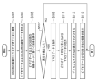
- FIG. 5 is a flowchart for explaining an example of the operation of the display system 1 according to the first embodiment. Below, an example of the operation of the display system 1 will be explained according to the flowchart shown in FIG. 5.
- the multiplexer 108 superimposes image data for OSD on the video data (S101).
- the multiplexer 108 outputs the video data and image data for OSD to the display device 20 (S103).
- the display device 20 displays an image based on the video data and image data for OSD output in S103 (S105). As a result, a screen including an OSD character image is displayed on the display panel 200 of the display device 20.
- the fail-safe controller 102 determines whether or not the detection circuit 100 has detected an abnormality related to the display of an image on the display device 20 (S107). If the fail-safe controller 102 determines in S107 that the detection circuit 100 has not detected an abnormality, the flowchart shown in FIG. 5 ends. On the other hand, if the fail-safe controller 102 determines in S107 that the detection circuit 100 has detected an abnormality, the process proceeds to S109.
- the OSD control circuit 110 accordingly generates mask data (S109). Specifically, the OSD mask circuit 118 generates mask data and transmits the mask data to the multiplexer 108.
- the multiplexer 108 switches the video data and outputs the mask data generated in S109 to the display device 20 (S111).
- the display device 20 then masks the display on the display panel 200 based on the mask data output in S111 (S113). As a result, the image based on the video data and the OSD character image are no longer displayed on the display panel 200.
- the display device 20 then displays the image after the video data has been switched (S115).
- in-vehicle meter cluster panels have increasingly been made to use liquid crystal displays.
- indicator and warning lights that were previously displayed using separate LEDs (Light Emitting Diodes) are now displayed on the same LCD.
- indicator and warning lights provide particularly important information to drivers, it is desirable for them to be controlled by a controller (microcomputer) that is independent of the GPU that displays other information.
- OSD OSD
- the IC Integrated Circuit
- FIGS. 6A to 6C are diagrams for explaining an example in which the display coordinates of the OSD are shifted at the timing of a transition.
- FIG. 6A is a diagram showing an image displayed on the display panel before the transition.
- FIG. 6B is a diagram showing an image to be displayed on the display panel after the transition.
- FIG. 6C is a diagram showing an image that may be displayed on the display panel during the transition.
- the timing controller 10 has a circuit that generates mask data for masking the image displayed on the display device 20, including the OSD character image, during image transitions. As a result, the image shown in FIG. 6C is masked on the display panel. In this way, the display system 1 according to this embodiment can achieve higher functional safety by monitoring the image and enabling independent operation.
- Second Embodiment 2 is a block diagram for explaining a timing controller 40 according to the second embodiment.
- the timing controller 40 according to the second embodiment is different from the timing controller 10 according to the first embodiment in that it mainly includes a synchronization signal generating circuit 105 and a multiplexer 107, and does not include an OSD mask circuit 118.
- FIG. 2 the same reference numerals are given to components having substantially the same functions as those in the first embodiment, and the description thereof is omitted as appropriate.
- the processing related to the mask data described in the first embodiment may not be performed.
- the timing controller 40 includes a detection circuit 100, a fail-safe controller 102, a memory controller 104, a synchronization signal generation circuit 105 (generation unit), multiplexers 106, 107, and 408, and an OSD control circuit 410.
- the synchronization signal generation circuit 105 generates a synchronization signal S9 for the video data output from the multiplexer 408, and outputs the synchronization signal S9 to the multiplexer 107.
- the video data can be synchronized with other video data.
- the synchronization signal generation circuit 105 may generate a synchronization signal S9 for the video data before the switching.
- the synchronization signal generation circuit 105 may generate a synchronization signal S9 for the video data before the switching in response to the detection circuit 100 detecting an abnormality related to the display of the display device 20.
- this synchronization signal S9 it is possible to synchronize the video data after the switching with the video data before the switching.
- the multiplexer 107 combines information from the graphic controller 16 and the synchronization signal generation circuit 105, and outputs data S10 to the multiplexer 408.
- the multiplexer 107 can output video data S1 from the graphic controller to the multiplexer 408. It can also output the synchronization signal S9 generated by the synchronization signal generation circuit 105 to the multiplexer 408.
- the OSD control circuit 410 acquires various data related to the OSD and transmits the generated image data D3 to the multiplexer 408.
- the OSD control circuit 410 has an OSD controller 112, an internal memory 114, and an OSD generation circuit 116.
- the OSD generation circuit 116 generates image data D3 for OSD and transmits the image data D3 to the multiplexer 408. Specifically, the OSD generation circuit 116 can refer to information about characters for OSD stored in the internal memory 114 and generate image data D3 for the OSD characters based on that information.
- the multiplexer 408 outputs the video data and image data for OSD to the display device 20.
- the multiplexer 408 superimposes image data D3 of OSD characters onto the video data S1 using various known techniques. For example, the multiplexer 408 may replace the luminance value of an area of the video data S1 where the image data D3 for OSD should be overlaid with the luminance value of the image data D3 for OSD.
- the output data S11 which includes the video data that has been processed by the multiplexer 408, is transmitted to the display device 20.
- the multiplexer 408 can also switch the video data to be output.
- the multiplexer 408 may switch the video data to be output in response to an abnormality being detected in the detection circuit 100. Specifically, when an abnormality is detected, the multiplexer 408 may switch the video data so that the display on the display device 20 transitions from a normal image to a black image (a fail-safe image).
- the multiplexer 408 when switching the video data to be output to the display device 20, the multiplexer 408 outputs a synchronization signal S9 of the video data before switching to the display device 20 together with the video data after switching. This allows the display device 20 to display an image based on the video data after switching that is synchronized with the video data before switching. Furthermore, by using this synchronization signal S9, positional deviation of the image based on the image data for OSD is suppressed when switching the video data.
- Figure 8A is a diagram showing an example of an image normally displayed on the display device 20
- Figure 8C is a diagram showing an example of an image to be displayed on the display device 20 after an abnormality related to the display on the display device 20 is detected
- Figure 8B is a diagram showing an example of an image displayed on the display device 20 when transitioning from the image shown in Figure 8A to the image shown in Figure 8C.
- OSD character image is displayed along with an image showing a speedometer, etc.
- OSD character images 50, 52 representing various warning lights and indicator lights are displayed at the top and bottom of the screen. Examples of half-open doors, warning lights and indicator lights include those relating to the handbrake and seat belt.
- OSD character image 54 showing the driving status of the vehicle
- OSD image 56 showing the vehicle's speed.
- the video data is switched so that the image displayed on the display device 20 transitions from the image shown in FIG. 8A to the image shown in FIG. 8C.
- the image based on the video data after the switch is an image in which an OSD character image 50 is displayed on a black image.
- images are drawn in sequence from the top to the bottom of the screen based on the video data, as shown by the drawing directions in Figures 8A to 8C.
- images are drawn down to the bottom of the screen, images are drawn in sequence from the top to the bottom based on the video data.
- the total length of the screen in the drawing direction is taken as L1.
- an image is drawn in area A1 from the top of the screen to a position L2 ( ⁇ L1) in the drawing direction based on the video data before the switch, and at that timing the video data is switched to the video data after the switch. Therefore, in the area below area A1 shown in Figure 8A, an image is displayed based on the video data after the switch.
- the video data after switching is synchronized with the video data before switching based on the synchronization signal. Therefore, as shown in FIG. 8B, the image of area A2 below area A1 shown in FIG. 8C is displayed in area A2 below area A1. Therefore, as shown in FIG. 8B, the OSD display, particularly the OSD character image 52 in area A2, is prevented from shifting position. As a result, images can be displayed appropriately when the display transitions on a display device that uses the OSD function.
- FIG. 9 is a flowchart for explaining an example of the operation of the display system 4 according to one embodiment of the present disclosure. Below, an example of the operation of the display system 4 will be explained according to the flowchart shown in FIG. 9.
- the multiplexer 408 superimposes image data for OSD on the video data (S201).
- the synchronization signal generation circuit 105 generates a synchronization signal S9 for the video data (S203).
- This synchronization signal S9 is a signal synchronized with the video data (video data before switching) on which the image data for OSD was superimposed in S201.
- the synchronization signal generation circuit 105 continues to generate the synchronization signal S9.
- the multiplexer 408 outputs the video data and the image data for OSD to the display device 20 (S205).
- the display device 20 displays an image based on the video data and the image data for OSD output in S205 (S207). As a result, a screen including an OSD character image is displayed on the display panel 200 of the display device 20.
- the synchronization signal generation circuit 105 determines whether or not the detection circuit 100 has detected an abnormality regarding the display of an image on the display device 20 (S209). If the synchronization signal generation circuit 105 determines in S209 that the detection circuit 100 has not detected an abnormality, the process of the flowchart shown in FIG. 9 ends. On the other hand, if the synchronization signal generation circuit 105 determines in S209 that the detection circuit 100 has detected an abnormality, the process proceeds to S211.
- the multiplexer 408 switches the video data and outputs a synchronization signal (S211).
- the display device 20 displays an image corresponding to the switched video data based on the synchronization signal (S213). As a result, an image is displayed based on the switched video data that is synchronized with the pre-switched video data.
- the process shown in FIG. 9 ends.
- Fig. 10 is a timing chart for explaining an example of the operation of the timing controller 40 according to the present embodiment.
- Fig. 10 shows input data D IN , a timing signal S T , video data D N in normal operation, a synchronization signal S S , video data D A in abnormal operation, an abnormality signal S A , and output data S11.
- the input data D IN is data input to the timing controller 40, including the video data S1 input from the graphic controller 16.
- the video data D N in the normal state is output from the multiplexer 408 to the display device 20 in accordance with the timing signal S T based on the input data D IN .
- the synchronous signal generating circuit 105 generates a synchronous signal S9 synchronized with the timing signal ST .
- This synchronous signal S9 is generated so that the rising timing (t1, t2, t4, t5) is the same as the rising timing of the timing signal ST .
- the video data DA in an abnormal state is output from the multiplexer 408 to the display device 20 together with this synchronous signal S9. As a result, the video data DA in an abnormal state is synchronized with the video data DN in a normal state.
- the abnormality signal S A is included in the signal S6 generated by the detection circuit 100.
- the abnormality signal S A is low, the normal video data D N is output, and when the abnormality signal S A is high, the abnormality video data D A is output.
- the normal video data D N is output until just before timing t3, the abnormality signal S A switches from low to high at timing t3, and the abnormality video data D A is output after timing t3.
- This video data D A is output together with a synchronization signal S9, and when switching from the normal video data D N to the abnormality video data D A , an image is displayed on the display device 20 so that the display positions of the images before and after the switching are synchronized. This suppresses positional deviation of the image on the display device 20 when switching the video data.
- in-vehicle meter cluster panels have increasingly been made to use liquid crystal displays.
- indicator and warning lights that were previously displayed using separate LEDs (Light Emitting Diodes) are now displayed on the same LCD.
- indicator and warning lights provide particularly important information to drivers, it is desirable for them to be controlled by a controller (microcomputer) that is independent of the GPU that displays other information.
- OSD OSD
- the IC Integrated Circuit
- FIGS. 11A to 11C are diagrams for explaining an example in which the OSD display coordinates are shifted at the timing of a transition.
- FIG. 11A is a diagram showing an image displayed on the display panel before the transition.
- FIG. 11B is a diagram showing an image to be displayed on the display panel after the transition.
- FIG. 11C is a diagram showing an image that may be displayed on the display panel during the transition.
- Images are drawn on the display panel in the drawing directions shown in Figures 11A to 11C, specifically from top to bottom, based on the video data and image data for OSD.
- the display transitions when area B1 of the image shown in Figure 11A is displayed on the display panel.
- the image in area B1 remains on the display panel, and area B2 of the image shown in Figure 11B is displayed in area B3 below.
- the video data before switching and the video data after switching can be synchronized using the synchronization signal S9, so that the positional deviation of the OSD display can be suppressed, as shown in FIG. 8B.
- the display system 4 of this embodiment by monitoring the image and enabling independent operation, higher functional safety can be achieved.
- Item 1 an output interface for outputting video data and image data for on-screen display (OSD) to be superimposed on the video data to a display device; an acquisition unit that acquires mask data for masking a display on the display device, the output interface outputs the mask data to the display device when switching the video data to be output to the display device, so that the display of the display device is masked at the time of a transition of the display on the display device in response to the switching of the video data.
- Display control device Display control device.
- a detection unit for detecting an abnormality related to the display of the display device is further provided.
- the output interface switches the video data to be output to the display device in response to the detection of the abnormality.
- Item 2 A display control device according to item 1.
- the display device masked based on the mask data displays a part of the image to be displayed on the display device based on the switched video data; 3.
- a display control device according to item 1 or 2.
- a display control device according to any one of items 1 to 3, The display device, The display on the display device is masked based on the mask data at the time of transition in response to the switching of the video data. Display system.
- the display device includes a meter cluster panel mounted on a vehicle. 5.
- the display of the display device masked based on the mask data includes an image that is displayed on the display device based on the switched video data and is not dependent on the running state of the automobile.
- Item 6 A display system according to item 5.
- an output interface for outputting video data and image data for on-screen display (OSD) to be superimposed on the video data to a display device; a generating unit that generates a synchronization signal for the video data output from the output interface, the output interface outputs, when switching the video data to be output to the display device, a synchronization signal of the video data before the switching together with the video data after the switching to the display device.
- Display control device
- a detection unit for detecting an abnormality related to the display of the display device is further provided.
- the output interface switches the video data to be output to the display device in response to the detection of the abnormality.
- Item 9 A display control device according to item 8.
- a display control device according to item 8 or 9
- the display device when switching the video data output from the output interface, displays an image corresponding to the switched video data based on a synchronization signal of the video data before the switching. Display system.
- the display device includes a meter cluster panel mounted on a vehicle. Item 11. A display system according to item 10.
- This disclosure relates to a display control device, an automobile using the same, and a display system.
Landscapes
- Engineering & Computer Science (AREA)
- Theoretical Computer Science (AREA)
- Physics & Mathematics (AREA)
- Computer Hardware Design (AREA)
- General Physics & Mathematics (AREA)
- Signal Processing (AREA)
- Multimedia (AREA)
- Chemical & Material Sciences (AREA)
- Combustion & Propulsion (AREA)
- Transportation (AREA)
- Mechanical Engineering (AREA)
- Controls And Circuits For Display Device (AREA)
- Control Of Indicators Other Than Cathode Ray Tubes (AREA)
Priority Applications (1)
| Application Number | Priority Date | Filing Date | Title |
|---|---|---|---|
| JP2024564319A JPWO2024128094A1 (https=) | 2022-12-14 | 2023-12-06 |
Applications Claiming Priority (4)
| Application Number | Priority Date | Filing Date | Title |
|---|---|---|---|
| JP2022199728 | 2022-12-14 | ||
| JP2022-199728 | 2022-12-14 | ||
| JP2023013203 | 2023-01-31 | ||
| JP2023-013203 | 2023-01-31 |
Publications (1)
| Publication Number | Publication Date |
|---|---|
| WO2024128094A1 true WO2024128094A1 (ja) | 2024-06-20 |
Family
ID=91484949
Family Applications (1)
| Application Number | Title | Priority Date | Filing Date |
|---|---|---|---|
| PCT/JP2023/043658 Ceased WO2024128094A1 (ja) | 2022-12-14 | 2023-12-06 | 表示制御装置、それを用いた自動車、表示システム |
Country Status (2)
| Country | Link |
|---|---|
| JP (1) | JPWO2024128094A1 (https=) |
| WO (1) | WO2024128094A1 (https=) |
Citations (5)
| Publication number | Priority date | Publication date | Assignee | Title |
|---|---|---|---|---|
| JP2002196276A (ja) * | 2000-12-25 | 2002-07-12 | Minolta Co Ltd | 車両用表示装置 |
| JP2013105171A (ja) * | 2011-11-17 | 2013-05-30 | Seiko Epson Corp | プロジェクター及びその制御方法 |
| US20140362448A1 (en) * | 2013-06-11 | 2014-12-11 | Honda Motor Co., Ltd. | Hud fusion interface |
| JP2017210233A (ja) * | 2016-05-19 | 2017-11-30 | カルソニックカンセイ株式会社 | 車両用情報表示装置 |
| JP2022037952A (ja) * | 2020-08-26 | 2022-03-10 | セイコーエプソン株式会社 | 回路装置、電子機器及びエラー検出方法 |
-
2023
- 2023-12-06 WO PCT/JP2023/043658 patent/WO2024128094A1/ja not_active Ceased
- 2023-12-06 JP JP2024564319A patent/JPWO2024128094A1/ja active Pending
Patent Citations (5)
| Publication number | Priority date | Publication date | Assignee | Title |
|---|---|---|---|---|
| JP2002196276A (ja) * | 2000-12-25 | 2002-07-12 | Minolta Co Ltd | 車両用表示装置 |
| JP2013105171A (ja) * | 2011-11-17 | 2013-05-30 | Seiko Epson Corp | プロジェクター及びその制御方法 |
| US20140362448A1 (en) * | 2013-06-11 | 2014-12-11 | Honda Motor Co., Ltd. | Hud fusion interface |
| JP2017210233A (ja) * | 2016-05-19 | 2017-11-30 | カルソニックカンセイ株式会社 | 車両用情報表示装置 |
| JP2022037952A (ja) * | 2020-08-26 | 2022-03-10 | セイコーエプソン株式会社 | 回路装置、電子機器及びエラー検出方法 |
Also Published As
| Publication number | Publication date |
|---|---|
| JPWO2024128094A1 (https=) | 2024-06-20 |
Similar Documents
| Publication | Publication Date | Title |
|---|---|---|
| JP5507090B2 (ja) | 表示装置 | |
| US11250766B2 (en) | Semiconductor apparatus | |
| US11186294B2 (en) | In-vehicle timing controller and vehicle using the same | |
| CN110718198B (zh) | 显示装置及其驱动方法 | |
| US12062309B2 (en) | Device and method for detecting screen freeze error of display of vehicle | |
| US11620926B2 (en) | Abnormality detection circuit | |
| US11263986B2 (en) | System and method for display fault monitoring | |
| US20190237036A1 (en) | Display device | |
| JP2021026135A (ja) | 表示装置および検査方法 | |
| JP7649836B2 (ja) | 表示装置およびその駆動方法 | |
| WO2024128094A1 (ja) | 表示制御装置、それを用いた自動車、表示システム | |
| US11642964B2 (en) | Display device, electronic apparatus, and moving object | |
| US11657743B2 (en) | Display driver, electronic apparatus, and moving object | |
| KR20240057233A (ko) | 사용자 경고 이미지를 제공하는 차량 정보 제공 장치 및 디지털 클러스터 장치 | |
| US11056033B2 (en) | Electro-optical apparatus, display control system, display driver, electronic device, and mobile unit | |
| JP2018159796A (ja) | 液晶表示装置 | |
| US20070040789A1 (en) | Protection device for gate integrated circuit, gate driver, liquid crystal display including the same and method of protecting a gate IC in a display | |
| JP7793937B2 (ja) | 車両通知システム | |
| US11074843B2 (en) | Drive circuit, electro-optical device, electronic apparatus including electro-optical device, and movable body including electronic apparatus | |
| JP2025099470A (ja) | 半導体装置および表示システム | |
| JP2025099469A (ja) | 半導体装置および表示システム | |
| US20250266012A1 (en) | Driver circuit and image display system | |
| JP2023027419A (ja) | タイミングコントローラおよびディスプレイシステム、自動車 | |
| US11972077B1 (en) | Resetting system and method | |
| CN120245716A (zh) | 车载显示系统、车载显示屏的显示控制方法以及机动车辆 |
Legal Events
| Date | Code | Title | Description |
|---|---|---|---|
| 121 | Ep: the epo has been informed by wipo that ep was designated in this application |
Ref document number: 23903383 Country of ref document: EP Kind code of ref document: A1 |
|
| WWE | Wipo information: entry into national phase |
Ref document number: 2024564319 Country of ref document: JP |
|
| NENP | Non-entry into the national phase |
Ref country code: DE |
|
| 122 | Ep: pct application non-entry in european phase |
Ref document number: 23903383 Country of ref document: EP Kind code of ref document: A1 |