WO2024100925A1 - 高周波回路および増幅回路 - Google Patents
高周波回路および増幅回路 Download PDFInfo
- Publication number
- WO2024100925A1 WO2024100925A1 PCT/JP2023/025481 JP2023025481W WO2024100925A1 WO 2024100925 A1 WO2024100925 A1 WO 2024100925A1 JP 2023025481 W JP2023025481 W JP 2023025481W WO 2024100925 A1 WO2024100925 A1 WO 2024100925A1
- Authority
- WO
- WIPO (PCT)
- Prior art keywords
- circuit
- delay
- variable
- phase
- phase shift
- Prior art date
- Legal status (The legal status is an assumption and is not a legal conclusion. Google has not performed a legal analysis and makes no representation as to the accuracy of the status listed.)
- Ceased
Links
Images




Classifications
-
- H—ELECTRICITY
- H03—ELECTRONIC CIRCUITRY
- H03F—AMPLIFIERS
- H03F3/00—Amplifiers with only discharge tubes or only semiconductor devices as amplifying elements
- H03F3/20—Power amplifiers, e.g. Class B amplifiers, Class C amplifiers
- H03F3/24—Power amplifiers, e.g. Class B amplifiers, Class C amplifiers of transmitter output stages
- H03F3/245—Power amplifiers, e.g. Class B amplifiers, Class C amplifiers of transmitter output stages with semiconductor devices only
-
- H—ELECTRICITY
- H01—ELECTRIC ELEMENTS
- H01Q—ANTENNAS, i.e. RADIO AERIALS
- H01Q21/00—Antenna arrays or systems
- H01Q21/06—Arrays of individually energised antenna units similarly polarised and spaced apart
- H01Q21/08—Arrays of individually energised antenna units similarly polarised and spaced apart the units being spaced along or adjacent to a rectilinear path
-
- H—ELECTRICITY
- H01—ELECTRIC ELEMENTS
- H01Q—ANTENNAS, i.e. RADIO AERIALS
- H01Q3/00—Arrangements for changing or varying the orientation or the shape of the directional pattern of the waves radiated from an antenna or antenna system
- H01Q3/26—Arrangements for changing or varying the orientation or the shape of the directional pattern of the waves radiated from an antenna or antenna system varying the relative phase or relative amplitude of energisation between two or more active radiating elements; varying the distribution of energy across a radiating aperture
-
- H—ELECTRICITY
- H01—ELECTRIC ELEMENTS
- H01Q—ANTENNAS, i.e. RADIO AERIALS
- H01Q3/00—Arrangements for changing or varying the orientation or the shape of the directional pattern of the waves radiated from an antenna or antenna system
- H01Q3/26—Arrangements for changing or varying the orientation or the shape of the directional pattern of the waves radiated from an antenna or antenna system varying the relative phase or relative amplitude of energisation between two or more active radiating elements; varying the distribution of energy across a radiating aperture
- H01Q3/2682—Time delay steered arrays
-
- H—ELECTRICITY
- H03—ELECTRONIC CIRCUITRY
- H03F—AMPLIFIERS
- H03F1/00—Details of amplifiers with only discharge tubes, only semiconductor devices or only unspecified devices as amplifying elements
- H03F1/02—Modifications of amplifiers to raise the efficiency, e.g. gliding Class A stages, use of an auxiliary oscillation
- H03F1/0205—Modifications of amplifiers to raise the efficiency, e.g. gliding Class A stages, use of an auxiliary oscillation in transistor amplifiers
- H03F1/0211—Modifications of amplifiers to raise the efficiency, e.g. gliding Class A stages, use of an auxiliary oscillation in transistor amplifiers with control of the supply voltage or current
- H03F1/0216—Continuous control
- H03F1/0222—Continuous control by using a signal derived from the input signal
-
- H—ELECTRICITY
- H03—ELECTRONIC CIRCUITRY
- H03F—AMPLIFIERS
- H03F3/00—Amplifiers with only discharge tubes or only semiconductor devices as amplifying elements
- H03F3/189—High-frequency amplifiers, e.g. radio frequency amplifiers
- H03F3/19—High-frequency amplifiers, e.g. radio frequency amplifiers with semiconductor devices only
- H03F3/195—High-frequency amplifiers, e.g. radio frequency amplifiers with semiconductor devices only in integrated circuits
-
- H—ELECTRICITY
- H03—ELECTRONIC CIRCUITRY
- H03F—AMPLIFIERS
- H03F3/00—Amplifiers with only discharge tubes or only semiconductor devices as amplifying elements
- H03F3/68—Combinations of amplifiers, e.g. multi-channel amplifiers for stereophonics
-
- H—ELECTRICITY
- H03—ELECTRONIC CIRCUITRY
- H03F—AMPLIFIERS
- H03F2200/00—Indexing scheme relating to amplifiers
- H03F2200/102—A non-specified detector of a signal envelope being used in an amplifying circuit
-
- H—ELECTRICITY
- H03—ELECTRONIC CIRCUITRY
- H03F—AMPLIFIERS
- H03F2200/00—Indexing scheme relating to amplifiers
- H03F2200/451—Indexing scheme relating to amplifiers the amplifier being a radio frequency amplifier
-
- H—ELECTRICITY
- H04—ELECTRIC COMMUNICATION TECHNIQUE
- H04B—TRANSMISSION
- H04B7/00—Radio transmission systems, i.e. using radiation field
- H04B7/02—Diversity systems; Multi-antenna system, i.e. transmission or reception using multiple antennas
- H04B7/04—Diversity systems; Multi-antenna system, i.e. transmission or reception using multiple antennas using two or more spaced independent antennas
- H04B7/06—Diversity systems; Multi-antenna system, i.e. transmission or reception using multiple antennas using two or more spaced independent antennas at the transmitting station
- H04B7/0613—Diversity systems; Multi-antenna system, i.e. transmission or reception using multiple antennas using two or more spaced independent antennas at the transmitting station using simultaneous transmission
- H04B7/0615—Diversity systems; Multi-antenna system, i.e. transmission or reception using multiple antennas using two or more spaced independent antennas at the transmitting station using simultaneous transmission of weighted versions of same signal
- H04B7/0617—Diversity systems; Multi-antenna system, i.e. transmission or reception using multiple antennas using two or more spaced independent antennas at the transmitting station using simultaneous transmission of weighted versions of same signal for beam forming
Definitions
- the present invention relates to high-frequency circuits and amplifier circuits.
- Patent Document 1 discloses a power amplifier device to which a variable power supply voltage is supplied using ET.
- the power amplifier device includes a power amplifier, a phase modulation circuit required for beamforming a high-frequency signal, which is disposed at the input stage of the power amplifier, and an amplitude modulation circuit for adjusting the amplitude of the variable power supply voltage.
- variable power supply voltage does not adequately correspond to the high-frequency signal input to the power amplifier, and there is a possibility that linearity will deteriorate due to deterioration of the EVM (Error Vector Magnitude) and ACLR (Adjacent Channel Leakage Power Ratio) of the high-frequency signal output from the power amplifier device.
- EVM Error Vector Magnitude
- ACLR Adjacent Channel Leakage Power Ratio
- the present invention provides a high-frequency circuit and an amplifier circuit in which degradation of linearity is suppressed.
- a high-frequency circuit comprises a first power amplifier and a second power amplifier that amplify a high-frequency signal, a tracker circuit configured to output a variable power supply voltage, a first variable phase-shift circuit connected to the input end of the first power amplifier and configured to vary the phase of the high-frequency signal, a second variable phase-shift circuit connected to the input end of the second power amplifier and configured to vary the phase of the high-frequency signal, an array antenna including a first antenna connected to the output end of the first power amplifier and a second antenna connected to the output end of the second power amplifier, a first variable delay circuit connected between the tracker circuit and the first power amplifier and configured to vary the amount of delay of the variable power supply voltage, and a second variable delay circuit connected between the tracker circuit and the second power amplifier and configured to vary the amount of delay of the variable power supply voltage.
- a radio frequency circuit includes a first power amplifier and a second power amplifier to which a variable power supply voltage is applied, a first variable phase shift circuit configured to vary the phase of a radio frequency signal input to the first power amplifier by a first phase shift amount, a second variable phase shift circuit configured to vary the phase of a radio frequency signal input to the second power amplifier by a second phase shift amount, an array antenna including a first antenna that radiates a radio frequency signal output from the first power amplifier and a second antenna that radiates a radio frequency signal output from the second power amplifier, a first variable delay circuit configured to add a first delay amount corresponding to the first phase shift amount to the variable power supply voltage applied to the first power amplifier, and a second variable delay circuit configured to add a second delay amount corresponding to the second phase shift amount to the variable power supply voltage applied to the second power amplifier.
- an amplifier circuit includes a first power amplifier and a second power amplifier that amplify a high-frequency signal, an external connection terminal that receives a variable power supply voltage according to the high-frequency signal, a first variable phase-shift circuit connected to the input terminal of the first power amplifier and configured to vary the phase of the high-frequency signal, a second variable phase-shift circuit connected to the input terminal of the second power amplifier and configured to vary the phase of the high-frequency signal, a first variable delay circuit connected between the external connection terminal and the first power amplifier and configured to vary the delay time of the variable power supply voltage, and a second variable delay circuit connected between the external connection terminal and the second power amplifier and configured to vary the delay time of the variable power supply voltage.
- the present invention provides a high-frequency circuit and an amplifier circuit that suppress degradation of linearity.
- FIG. 1A is a graph showing an example of a transition of a power supply voltage in an analog envelope tracking mode.
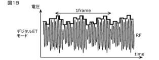
- FIG. 1B is a graph showing an example of the transition of the power supply voltage in the digital envelope tracking mode.
- FIG. 2 is a circuit configuration diagram of a high-frequency circuit according to an embodiment.
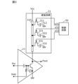
- FIG. 3 is a circuit diagram showing an example of a delay circuit and its peripheral circuits according to an embodiment.
- FIG. 4 is a diagram showing the relationship between antenna arrangement and beam radiation direction in the high-frequency circuit according to the embodiment.
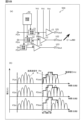
- FIG. 5A is a diagram illustrating the relationship between a high-frequency signal input/output to/from an amplifier circuit according to an embodiment and a variable power supply voltage.
- FIG. 5B is a diagram illustrating the relationship between the high frequency signal input/output to/from the amplifier circuit according to the comparative example and the variable power supply voltage.
- each figure is a schematic diagram in which emphasis, omissions, or adjustments to the ratio have been made as appropriate to illustrate the present invention, and is not necessarily an exact illustration, and may differ from the actual shape, positional relationship, and ratio.
- the same reference numerals are used for substantially the same configuration, and duplicate explanations may be omitted or simplified.
- connection includes not only direct connection by connection terminals and/or wiring conductors, but also electrical connection via other circuit elements.
- Connected between A and B means connected to both A and B between A and B.
- a “signal path” refers to a transmission line that is composed of a wiring through which a high-frequency signal propagates, an electrode directly connected to the wiring, and a terminal directly connected to the wiring or the electrode.
- the tracking mode which supplies a power amplifier with a variable power supply voltage that is dynamically adjusted over time based on the high-frequency signal.
- the tracking mode is a mode in which the power supply voltage applied to the amplifier circuit is dynamically adjusted.
- envelope tracking (ET) mode including analog ET mode and digital ET mode
- SPT symbol power tracking
- Figures 1A and 1B the horizontal axis represents time and the vertical axis represents voltage.
- the thick solid line represents the power supply voltage
- the thin solid line (waveform) represents the modulated wave.
- FIG. 1A is a graph showing an example of the transition of the power supply voltage in analog ET mode.
- Analog ET mode is an example of ET mode.
- the envelope of the modulated wave is tracked by continuously varying the power supply voltage.
- the power supply voltage is determined based on the envelope signal.
- the envelope signal is a signal that indicates the envelope of a modulated wave.
- the envelope value is expressed, for example, as the square root of (I 2 +Q 2 ).
- (I, Q) represents a constellation point.
- a constellation point is a point that represents a signal modulated by digital modulation on a constellation diagram.
- (I, Q) is determined, for example, by a BBIC (BaseBand Integrated Circuit) based on transmission information.
- BBIC BaseBand Integrated Circuit
- FIG. 1B is a graph showing an example of the progression of the power supply voltage in digital ET mode.
- the envelope of the modulated wave is tracked by varying the power supply voltage to multiple discrete voltage levels within one frame.
- the power supply voltage signal forms a square wave.
- the power supply voltage level is selected or set from multiple discrete voltage levels based on the envelope signal.
- the power supply voltage is varied in symbol units smaller than one frame based on the average output power.
- a frame is a unit of high-frequency signals having a length of 10 milliseconds and includes 10 subframes.
- a subframe is a unit of high-frequency signals having a length of 1 millisecond and includes two slots.
- a slot is a unit of high-frequency signals having a length of 0.5 milliseconds and includes six or seven symbols.
- a symbol is a unit of high-frequency signals having a length of, for example, 71 microseconds and includes a cyclic prefix (CP).
- CP cyclic prefix
- the power supply voltage level is modulated on a symbol-by-symbol basis.
- the voltage level is changed in the CP section. For example, in the first symbol, the voltage level is changed to a higher voltage level in the CP, and in the second symbol, the voltage level is changed to a lower voltage level in the CP. Note that the voltage level does not have to be changed in subsequent symbols.
- the power supply voltage level can be modulated based on the data signal in each symbol section.
- FIG. 2 is a circuit diagram of the high-frequency circuit 5 according to the embodiment.
- the high-frequency circuit 5 according to the embodiment corresponds to a user terminal (UE: User Equipment) in a cellular network, and is typically a mobile phone, a smartphone, a tablet computer, a wearable device, etc.
- UE User Equipment
- the high-frequency circuit 5 may also be an IoT (Internet of Things) sensor device, a medical/healthcare device, a car, an unmanned aerial vehicle (UAV: Unmanned Aerial Vehicle) (a.k.a. a drone), or an automated guided vehicle (AGV: Automated Guided Vehicle).
- UAV Unmanned Aerial Vehicle
- AGV Automated Guided Vehicle
- the high-frequency circuit 5 in this embodiment includes an amplifier circuit 1, a tracker circuit 2, a signal processing circuit 3, and antennas 4a, 4b, and 4c.
- the signal processing circuit 3 is an example of a signal processing circuit that processes high-frequency signals.
- the signal processing circuit 3 has a control unit that controls the amplifier circuit 1 and the tracker circuit 2. Specifically, the signal processing circuit 3 processes the transmission signal by up-conversion or the like, and outputs the high-frequency signal generated by this signal processing to the amplifier circuit 1.
- the signal processing circuit 3 also outputs an envelope signal, which is a signal that indicates the envelope of the modulated wave of the high-frequency signal, to the tracker circuit 2. Furthermore, the signal processing circuit 3 outputs beam control signals s1, s2, and s3, which indicate the radiation direction of the output beam of the high-frequency signal output from the antennas 4a to 4c, to the amplifier circuit 1.
- control unit of the signal processing circuit 3 may be implemented outside the signal processing circuit 3, for example, in the amplifier circuit 1 and the tracker circuit 2.
- the tracker circuit 2 is configured to output a variable power supply voltage Vcc based on a tracking mode to the amplifier circuit 1.
- the tracking modes that can be used are analog ET mode, digital ET mode, and SPT mode.
- FIG. 2 illustrates a circuit configuration that outputs multiple discrete variable power supply voltages when the digital ET mode is applied.
- the tracker circuit 2 includes a discrete voltage generation circuit 60, a voltage selection circuit 70, and a digital control circuit 80.
- the discrete voltage generating circuit 60 is configured to generate a plurality of discrete voltages, each having a plurality of discrete voltage levels.
- the discrete voltage generating circuit 60 is, for example, a switched capacitor circuit including a plurality of capacitors and a plurality of switches.
- the voltage selection circuit 70 is configured to selectively output at least one of the multiple discrete voltages generated by the discrete voltage generation circuit 60 based on the envelope signal to the amplifier circuit 1.
- the voltage selection circuit 70 is controlled based on a digital control signal output from the digital control circuit 80. In other words, when the digital ET mode is applied, the tracker circuit 2 outputs multiple discrete variable power supply voltages based on the envelope value of the high-frequency signal.
- the digital control circuit 80 can control the voltage selection circuit 70 based on the envelope signal from the signal processing circuit 3. Specifically, the digital control circuit 80 generates a digital logic (DCL: Digital Control Logic/Line) signal based on the envelope signal received from the signal processing circuit 3.
- DCL Digital Control Logic/Line
- the digital control circuit 80 may not be included in the tracker circuit 2, but may be included in the signal processing circuit 3.
- Antenna 4a is an example of a first antenna, and is connected to the output end of power amplifier 11 via antenna connection terminal 101, and radiates the first high-frequency signal output from power amplifier 11.
- Antenna 4b is an example of a second antenna, and is connected to the output end of power amplifier 12 via antenna connection terminal 102, and radiates the second high-frequency signal output from power amplifier 12.
- Antenna 4c is connected to the output end of power amplifier 13 via antenna connection terminal 103, and radiates the third high-frequency signal output from power amplifier 13.
- the antennas 4a to 4c form an array antenna, and for example, the antennas 4a to 4c are arranged at equal intervals, and the radiation surfaces of the antennas 4a to 4c are arranged on the same plane.
- the first high-frequency signal, the second high-frequency signal, and the third high-frequency signal form a single output beam (radiation beam) with directionality.
- the arrangement of the antennas 4a to 4c will be described later with reference to Figure 4.
- the array antenna of the high frequency circuit 5 is not limited to three antennas 4a to 4c, but may have two or more antennas.
- the amplifier circuit 1 includes power amplifiers 11, 12, and 13, phase shift circuits 21, 22, and 23, delay circuits 31, 32, and 33, a DPD circuit 41, a preamplifier 14, a distributor 42, a signal input terminal 100, antenna connection terminals 101, 102, and 103, a power supply voltage terminal 110, and beam control terminals 120, 130, and 140.
- the signal input terminal 100 is connected to the signal processing circuit 3 and transmits the high-frequency signal output from the signal processing circuit 3 to the phase shift circuits 21-23 and the power amplifiers 11-13.
- Antenna connection terminal 101 is connected to power amplifier 11 and antenna 4a, and transmits the first high-frequency signal amplified by power amplifier 11 to antenna 4a.
- Antenna connection terminal 102 is connected to power amplifier 12 and antenna 4b, and transmits the second high-frequency signal amplified by power amplifier 12 to antenna 4b.
- Antenna connection terminal 103 is connected to power amplifier 13 and antenna 4c, and transmits the third high-frequency signal amplified by power amplifier 13 to antenna 4c.
- the power supply voltage terminal 110 is an example of an external connection terminal of the amplifier circuit 1, and is connected to the tracker circuit 2, to the power amplifier 11 via the delay circuit 31, to the power amplifier 12 via the delay circuit 32, and to the power amplifier 13 via the delay circuit 33. With this connection configuration, the power supply voltage terminal 110 transmits the variable power supply voltage Vcc generated by the tracker circuit 2 to the power amplifiers 11 to 13.
- the amplifier circuit 1 receives multiple discrete variable power supply voltages from the tracker circuit 2 via the power supply voltage terminal 110.
- the beam control terminal 120 transmits a beam control signal s1 indicating the radiation direction of the output beam of the high frequency signal formed by the antennas 4a to 4c to the amplifier circuit 1.
- the beam control terminal 130 transmits a beam control signal s2 indicating the radiation direction of the output beam of the high frequency signal formed by the antennas 4a to 4c to the amplifier circuit 1.
- the beam control terminal 140 transmits a beam control signal s3 indicating the radiation direction of the output beam of the high frequency signal formed by the antennas 4a to 4c to the amplifier circuit 1.
- the beam control signal output from the signal processing circuit 3 may be a digital control signal. When the beam control signal is a digital control signal, the signal processing circuit 3 may output only one beam control signal, in which case, for example, there may be two beam control terminals.
- the power amplifier 11 is an example of a first power amplifier, and amplifies a high-frequency signal input from a signal input terminal 100.
- the input terminal of the power amplifier 11 is connected to the phase shift circuit 21, the output terminal is connected to the antenna connection terminal 101, and the power supply input terminal is connected to the delay circuit 31.
- the power amplifier 12 is an example of a second power amplifier, and amplifies the high-frequency signal input from the signal input terminal 100.
- the input terminal of the power amplifier 12 is connected to the phase shift circuit 22, the output terminal is connected to the antenna connection terminal 102, and the power supply input terminal is connected to the delay circuit 32.
- the power amplifier 13 amplifies the high-frequency signal input from the signal input terminal 100.
- the input terminal of the power amplifier 13 is connected to the phase shift circuit 23, the output terminal is connected to the antenna connection terminal 103, and the power supply input terminal is connected to the delay circuit 33.
- Each of the power amplifiers 11 to 13 has an amplifying transistor.
- the amplifying transistor is, for example, a bipolar transistor such as a heterojunction bipolar transistor (HBT) or a field effect transistor such as a metal-oxide-semiconductor field effect transistor (MOSFET).
- HBT heterojunction bipolar transistor
- MOSFET metal-oxide-semiconductor field effect transistor
- Each of the power amplifiers 11 to 13 may have two amplification transistors connected in cascode. By having each of the power amplifiers 11 to 13 in a cascode connection configuration, the amplifier circuit 1 can ensure high amplification gain even for high-frequency signals in the millimeter wave band and sub-terahertz band.
- the DPD circuit 41 is connected to the signal input terminal 100, and has the function of performing amplitude-amplitude conversion and/or amplitude-phase conversion on the high-frequency signal output from the signal processing circuit 3 in advance to impart distortion components to the high-frequency signal in order to improve the linearity of the high-frequency signal output from the power amplifiers 11-13. This makes it possible to cancel out the signal distortion characteristics of the power amplifiers 11-13 and the distortion components of the high-frequency signal generated by the DPD circuit 41, thereby improving the linearity of the high-frequency signal output from the power amplifiers 11-13.
- the preamplifier 14 has an input terminal connected to the DPD circuit 41 and an output terminal connected to the distributor 42, and amplifies the high-frequency signal output from the DPD circuit 41.
- the distributor 42 distributes the power of the high-frequency signal output from the preamplifier 14 into three high-frequency signals, and outputs the three high-frequency signals to the phase-shift circuits 21 to 23, respectively.
- the DPD circuit 41 and the preamplifier 14 may be omitted.
- the distributor 42 may be included in the signal processing circuit 3.
- Phase-shift circuit 21 is an example of a first variable phase-shift circuit, is connected to the input terminal of power amplifier 11, and is configured to vary the phase of the high-frequency signal input to phase-shift circuit 21.
- Phase-shift circuit 22 is an example of a second variable phase-shift circuit, is connected to the input terminal of power amplifier 12, and is configured to vary the phase of the high-frequency signal input to phase-shift circuit 22.
- Phase-shift circuit 23 is connected to the input terminal of power amplifier 13, and is configured to vary the phase of the high-frequency signal input to phase-shift circuit 23.
- Delay circuit 31 is an example of a first variable delay circuit, is connected between tracker circuit 2 and power amplifier 11, and is configured to vary the amount of delay of the variable power supply voltage Vcc output from tracker circuit 2.
- Delay circuit 32 is an example of a second variable delay circuit, is connected between tracker circuit 2 and power amplifier 12, and is configured to vary the amount of delay of the variable power supply voltage Vcc output from tracker circuit 2.
- Delay circuit 33 is connected between tracker circuit 2 and power amplifier 13, and is configured to vary the amount of delay of the variable power supply voltage Vcc output from tracker circuit 2.
- the supply timing of the variable power supply voltage supplied to the power amplifiers 11-13 can be adjusted by the delay circuits 31-33, so degradation of the EVM, ACLR, etc. of the high frequency signal output from the antennas 4a-4c can be suppressed, and linearity can be improved.
- variable delay amount of each of the delay circuits 31 to 33 corresponds to the phase delay Td (sec) or group delay Tgd (sec) of the variable power supply voltage Vcc.
- Equation 2 the group delay Tgd( ⁇ ) (sec) is expressed, for example, by Equation 2.
- the control circuit 50 is connected to the beam control terminals 120-140, the phase shift circuits 21-23, and the delay circuits 31-33. Based on the beam control signal s1, the control circuit 50 outputs a phase control signal s21 (first phase control signal) indicating the first phase shift amount to the phase shift circuit 21, and outputs a delay control signal s31 (first delay control signal) indicating the first delay amount corresponding to the first phase shift amount to the delay circuit 31. Based on the beam control signal s2, the control circuit 50 outputs a phase control signal s22 (second phase control signal) indicating the second phase shift amount to the phase shift circuit 22, and outputs a delay control signal s32 (second delay control signal) indicating the second delay amount corresponding to the second phase shift amount to the delay circuit 32.
- a phase control signal s21 first phase control signal
- a delay control signal s31 first delay control signal
- the control circuit 50 Based on the beam control signal s3, the control circuit 50 outputs a phase control signal s23 indicating the third phase shift amount to the phase shift circuit 23, and outputs a delay control signal s33 indicating the third delay amount corresponding to the third phase shift amount to the delay circuit 33.
- the delay circuit 31 receives a delay control signal s31 from the control circuit 50 and adds a first delay amount corresponding to the first phase shift amount of the phase shift circuit 21 to the variable power supply voltage Vcc.
- the delay circuit 32 receives a delay control signal s32 from the control circuit 50 and adds a second delay amount corresponding to the second phase shift amount of the phase shift circuit 22 to the variable power supply voltage Vcc.
- the delay circuit 33 receives a delay control signal s33 from the control circuit 50 and adds a third delay amount corresponding to the third phase shift amount of the phase shift circuit 23 to the variable power supply voltage Vcc.
- the timing of the variable power supply voltage supplied to the power amplifiers 11 to 13 is adjusted to correspond to the phase shift amount of the phase shift circuits 21 to 23, making it possible to suppress deterioration of the EVM and ACLR of the high-frequency signals output from the antennas 4a to 4c and improve linearity.
- FIG. 3 is a circuit diagram showing an example of a delay circuit 31 and its peripheral circuitry according to an embodiment. The diagram shows the circuit configuration and connection configuration of the delay circuit 31, the power amplifier 11, and the control circuit 50.
- the power amplifier 11 has a transistor, a resistor, and a capacitor.
- the transistor is, for example, an n-type bipolar transistor (amplifying element).
- the base of the transistor is connected to the input terminal (Pin) via a first capacitor, the emitter of the transistor is connected to ground, and the collector of the transistor is connected to the output terminal (Pout) and the delay circuit 31.
- a second capacitor is connected between the base and emitter of the transistor.
- the delay circuit 31 includes a wiring 310, switches 311, 321, and 331, and capacitors 312, 322, and 332.
- a series-connected circuit of the switch 311 and the capacitor 312, a series-connected circuit of the switch 321 and the capacitor 322, and a series-connected circuit of the switch 331 and the capacitor 332 are each connected between the wiring 310 and the ground. Each series-connected circuit is connected to a different position of the wiring 310.
- the switch 311 is switched between conductive and non-conductive by a delay control signal s31 from the control circuit 50.
- the switch 321 is switched between conductive and non-conductive by a delay control signal s32 from the control circuit 50.
- the switch 331 is switched between conductive and non-conductive by a delay control signal s33 from the control circuit 50.
- the delay control signals s31, s32, and s33 correspond to the gate signals of the switches 311, 321, and 331. According to the above configuration, by switching the switches 311, 321, and 331, the position where the capacitor is connected in the wiring 310 is changed, thereby changing the amount of delay added to the variable power supply voltage Vcc transmitted through the wiring 310.
- the circuit configuration of the delay circuit 31 is not limited to the above circuit configuration example.
- any configuration that allows the electrical length of the wiring 310 to be varied may be used, and an inductor may be used instead of the wiring 310.
- a variable capacitor such as a Digitally Tunable Capacitor (DTC) may be used instead of the three series-connected circuits described above.
- DTC Digitally Tunable Capacitor
- delay circuits 32 and 33 have the same circuit configuration as delay circuit 31.
- [2 Relationship between antenna arrangement and beam radiation direction] 4 is a diagram showing the relationship between antenna arrangement and beam radiation direction in the high-frequency circuit 5 according to the embodiment.
- the antennas 4a to 4c constitute an array antenna, and their radiation surfaces are arranged on one plane, and are arranged in a straight line on the plane at a distance d.
- the high-frequency signals radiated from the antennas 4a to 4c are converted into signals having radiation directivity with a beam angle ⁇ by controlling the amplitude and phase of the excitation current and voltage input to the antennas 4a to 4c.
- the beam angle ⁇ is defined as the angle between the normal direction of the radiation surfaces of the antennas 4a to 4c and the radiation direction of the output beams formed by the antennas 4a to 4c.
- the propagation path x of the high frequency signal output from antenna 4a (first high frequency signal) is longer by d x sin ⁇ than the propagation path x of the high frequency signal output from antenna 4b (second high frequency signal).
- the propagation path x of the high frequency signal output from antenna 4b (second high frequency signal) is longer by d x sin ⁇ than the propagation path x of the high frequency signal output from antenna 4c (third high frequency signal).
- the phase of the second high frequency signal is delayed by a phase difference ⁇ from the phase of the first high frequency signal
- the phase of the third high frequency signal is delayed by a phase difference ⁇ from the phase of the second high frequency signal.
- the phase difference ⁇ is expressed by Equation 3.
- Equation 3 when the beam angle ⁇ is between 0° and 90°, the larger the beam angle ⁇ , the larger the phase difference ⁇ .
- Equation 3 if the first shift amount of phase shift circuit 21 is 0, the second shift amount of phase shift circuit 22 is ⁇ (a delay by), and the third shift amount of phase shift circuit 23 is 2 ⁇ (a delay by).
- phase shift circuits 21 to 23 vary the amount of phase shift of the first to third high frequency signals based on the radiation direction of the output beams formed by the antennas 4a to 4c.
- Fig. 5A is a diagram showing the relationship between a high frequency signal input/output to/from an amplifier circuit 1 according to an embodiment and a variable power supply voltage Vcc
- Fig. 5B is a diagram showing the relationship between a high frequency signal input/output to/from an amplifier circuit 500 according to a comparative example and a variable power supply voltage Vcc.
- FIG. 5A shows the phase difference ⁇ and delay difference ⁇ t when an amplifier circuit 1 according to an embodiment emits a radio frequency signal with a beam angle ⁇
- FIG. 5A shows the relationship between the radio frequency signals P1in, P2in, and P3in input to the power amplifiers 11 to 13, the radio frequency signals P1out, P2out, and P3out output from the power amplifiers 11 to 13, and the variable power supply voltage Vcc supplied to the power amplifiers 11 to 13.
- FIG. 5B (a) shows the phase difference ⁇ when a radio frequency signal with a beam angle ⁇ is emitted in the amplifier circuit 500 according to the comparative example
- FIG. 5B (b) shows the relationship between the radio frequency signals P1in, P2in, and P3in input to the power amplifiers 11 to 13, the radio frequency signals P1out, P2out, and P3out output from the power amplifiers 11 to 13, and the variable power supply voltage Vcc supplied to the power amplifiers 11 to 13.
- the amplifier circuit 500 according to the comparative example differs from the amplifier circuit 1 according to the embodiment only in that it does not include the delay circuits 31 to 33.
- the first to third phase shift amounts are generated in the phase shift circuits 21 to 23 so as to satisfy the phase difference ⁇ defined in Equation 3.
- the high-frequency signal P2out is delayed in phase by ⁇ from the high-frequency signal P1out
- the high-frequency signal P3out is delayed in phase by ⁇ from the high-frequency signal P2out.
- the variable power supply voltage Vcc is supplied to the power amplifiers 11 to 13 at the same timing.
- variable power supply voltage Vcc corresponding to the envelope values of the high-frequency signals P2out and P3out is not supplied to the power amplifiers 12 and 13. This causes the EVM and ACLR of the high-frequency signal output from the amplifier circuit 500 to deteriorate, and the linearity of the high-frequency signal to deteriorate.
- phase shift circuits 21 to 23 when a high-frequency signal with a beam angle ⁇ is radiated from antennas 4a to 4c, first to third phase shift amounts are generated in phase shift circuits 21 to 23 so as to satisfy the phase difference ⁇ defined in equation 3.
- a delay difference ⁇ t corresponding to the phase difference ⁇ is generated in delay circuits 31 to 33.
- the control circuit 50 executes the following control.
- the control circuit 50 when outputting phase control signals s21, s22, and s23 with a phase difference ⁇ of ⁇ 1 to achieve a beam angle ⁇ 1, the control circuit 50 outputs delay control signals s31, s32, and s33 with a delay difference ⁇ t of ⁇ t1.
- the control circuit 50 When realizing a beam angle ⁇ 2 larger than ⁇ 1, the control circuit 50 outputs phase control signals s21, s22, and s23 with a phase difference ⁇ of ⁇ 2 larger than ⁇ 1, and outputs delay control signals s31, s32, and s33 with a delay difference ⁇ t of ⁇ t2 larger than ⁇ t1.
- the phase difference ⁇ is increased from ⁇ 1 to ⁇ 2, and the delay difference ⁇ t is increased from ⁇ t1 to ⁇ t2. Also, when the beam angle ⁇ is decreased from ⁇ 2 to ⁇ 1, the phase difference ⁇ is decreased from ⁇ 2 to ⁇ 1, and the delay difference ⁇ t is decreased from ⁇ t2 to ⁇ t1.
- the timing of supplying the variable power supply voltage Vcc to the power amplifiers 11 to 13 is linked to the amount of phase shift of the high frequency signal, so that the variable power supply voltage Vcc corresponding to the envelope values of the high frequency signals P1out, P2out, and P3out is supplied to each of the power amplifiers 11 to 13.
- This suppresses deterioration of the EVM, ACLR, and other characteristics of the high frequency signal output from the amplifier circuit 1, and also suppresses deterioration of linearity.
- the high-frequency circuit 5 includes power amplifiers 11 and 12 that amplify high-frequency signals, a tracker circuit 2 configured to output a variable power supply voltage, a phase-shift circuit 21 connected to the input terminal of the power amplifier 11 and configured to vary the phase of the high-frequency signal, a phase-shift circuit 22 connected to the input terminal of the power amplifier 12 and configured to vary the phase of the high-frequency signal, an array antenna including an antenna 4a connected to the output terminal of the power amplifier 11 and an antenna 4b connected to the output terminal of the power amplifier 12, a delay circuit 31 connected between the tracker circuit 2 and the power amplifier 11 and configured to vary the amount of delay of the variable power supply voltage, and a delay circuit 32 connected between the tracker circuit 2 and the power amplifier 12 and configured to vary the amount of delay of the variable power supply voltage.
- the timing of the variable power supply voltage supplied to the power amplifiers 11 and 12 can be adjusted by the delay circuits 31 and 32, so degradation of the EVM, ACLR, etc. of the high frequency signals output from the antennas 4a and 4b can be suppressed, and linearity can be improved.
- the delay circuit 31 is configured to add a delay amount corresponding to the phase shift amount of the phase shift circuit 21 to the variable power supply voltage
- the delay circuit 32 is configured to add a delay amount corresponding to the phase shift amount of the phase shift circuit 22 to the variable power supply voltage.
- the timing of the variable power supply voltage supplied to the power amplifiers 11 and 12 is adjusted to correspond to the phase shift amount of the phase shift circuits 21 and 22, so that degradation of the EVM, ACLR, etc. of the high frequency signals output from the antennas 4a and 4b can be suppressed, and linearity can be improved.
- the high frequency circuit 5 further includes a control circuit 50 that outputs a phase control signal s21 indicating a first phase shift amount to the phase shift circuit 21, outputs a phase control signal s22 indicating a second phase shift amount to the phase shift circuit 22, outputs a delay control signal s31 indicating a first delay amount corresponding to the first phase shift amount to the delay circuit 31, and outputs a delay control signal s32 indicating a second delay amount corresponding to the second phase shift amount to the delay circuit 32.
- a control circuit 50 that outputs a phase control signal s21 indicating a first phase shift amount to the phase shift circuit 21, outputs a phase control signal s22 indicating a second phase shift amount to the phase shift circuit 22, outputs a delay control signal s31 indicating a first delay amount corresponding to the first phase shift amount to the delay circuit 31, and outputs a delay control signal s32 indicating a second delay amount corresponding to the second phase shift amount to the delay circuit 32.
- the control circuit 50 when the control circuit 50 outputs phase control signals s21 and s22 with the phase difference ⁇ set to ⁇ 1, it outputs delay control signals s31 and s32 with the delay difference ⁇ t set to ⁇ t1, and when the control circuit 50 outputs phase control signals s21 and s22 with the phase difference ⁇ set to ⁇ 2 larger than ⁇ 1, it outputs delay control signals s31 and s32 with the delay difference ⁇ t set to ⁇ t2 larger than ⁇ t1.
- the phase shift circuits 21 and 22 vary the amount of phase shift of the high-frequency signal based on the radiation direction of the output beams formed by the antennas 4a and 4b.
- the beam angle ⁇ of the high frequency signal can be adjusted by varying the amount of phase shift in the phase shift circuits 21 and 22.
- the tracker circuit 2 outputs multiple discrete variable power supply voltages based on the envelope value of the high-frequency signal.
- the high-frequency circuit 5 can amplify high-frequency signals using digital ET.
- the power amplifiers 11 and 12 can amplify high-frequency signals in the millimeter wave band or the sub-terahertz band.
- the amplifier circuit 1 also includes power amplifiers 11 and 12 to which a variable power supply voltage is applied, a phase shift circuit 21 configured to vary the phase of the high frequency signal input to the power amplifier 11 by a first phase shift amount, a phase shift circuit 22 configured to vary the phase of the high frequency signal input to the power amplifier 12 by a second phase shift amount, an array antenna including an antenna 4a that radiates the high frequency signal output from the power amplifier 11 and an antenna 4b that radiates the high frequency signal output from the power amplifier 12, a delay circuit 31 configured to add a first delay amount corresponding to the first phase shift amount to the variable power supply voltage applied to the power amplifier 11, and a delay circuit 32 configured to add a second delay amount corresponding to the second phase shift amount to the variable power supply voltage applied to the power amplifier 12.
- the timing of the variable power supply voltage supplied to the power amplifiers 11 and 12 is adjusted by the delay circuits 31 and 32 in accordance with the phase shift amount of the phase shift circuits 21 and 22, so that degradation of the EVM, ACLR, etc. of the high frequency signals output from the antennas 4a and 4b can be suppressed, and linearity can be improved.
- delay circuits 31 and 32 increase the delay difference ⁇ t, which is the amount obtained by subtracting the first delay amount from the second delay amount, as the phase difference ⁇ , which is the amount obtained by subtracting the first phase shift amount from the second phase shift amount, increases.
- the amplifier circuit 1 also includes power amplifiers 11 and 12 that amplify high-frequency signals, a power supply voltage terminal 110 which is an external connection terminal, a phase shift circuit 21 connected to the input terminal of the power amplifier 11 and configured to vary the phase of the high-frequency signal, a phase shift circuit 22 connected to the input terminal of the power amplifier 12 and configured to vary the phase of the high-frequency signal, a delay circuit 31 connected between the power supply voltage terminal 110 and the power amplifier 11 and configured to vary the amount of delay of the variable power supply voltage, and a delay circuit 32 connected between the power supply voltage terminal 110 and the power amplifier 12 and configured to vary the amount of delay of the variable power supply voltage.
- the timing of the variable power supply voltage supplied to the power amplifiers 11 and 12 can be adjusted by the delay circuits 31 and 32, so that deterioration of the EVM, ACLR, etc. of the high frequency signals output from the power amplifiers 11 and 12 can be suppressed, and linearity can be improved.
- the delay circuit 31 is configured to add a delay amount corresponding to the phase shift amount of the phase shift circuit 21 to the variable power supply voltage
- the delay circuit 32 is configured to add a delay amount corresponding to the phase shift amount of the phase shift circuit 22 to the variable power supply voltage.
- the supply timing of the variable power supply voltage supplied to the power amplifiers 11 and 12 is adjusted to correspond to the phase shift amount of the phase shift circuits 21 and 22, so that deterioration of the EVM, ACLR, etc. of the high frequency signals output from the power amplifiers 11 and 12 can be suppressed, and linearity can be improved.
- the amplifier circuit 1 further includes a control circuit 50 that outputs a phase control signal s21 indicating a first phase shift amount to the phase shift circuit 21, outputs a phase control signal s22 indicating a second phase shift amount to the phase shift circuit 22, outputs a delay control signal s31 indicating a first delay amount corresponding to the first phase shift amount to the delay circuit 31, and outputs a delay control signal s32 indicating a second delay amount corresponding to the second phase shift amount to the delay circuit 32.
- a control circuit 50 that outputs a phase control signal s21 indicating a first phase shift amount to the phase shift circuit 21, outputs a phase control signal s22 indicating a second phase shift amount to the phase shift circuit 22, outputs a delay control signal s31 indicating a first delay amount corresponding to the first phase shift amount to the delay circuit 31, and outputs a delay control signal s32 indicating a second delay amount corresponding to the second phase shift amount to the delay circuit 32.
- the control circuit 50 when the control circuit 50 outputs phase control signals s21 and s22 with the phase difference ⁇ being ⁇ 1, it outputs delay control signals s31 and s32 with the delay difference ⁇ t being ⁇ t1, and when the control circuit 50 outputs phase control signals s21 and s22 with the phase difference ⁇ being ⁇ 2, which is greater than ⁇ 1, it outputs delay control signals s31 and s32 with the delay difference ⁇ t being ⁇ t2, which is greater than ⁇ t1.
- the high-frequency circuit and amplifier circuit according to the present invention have been described above based on the embodiments, the high-frequency circuit and amplifier circuit according to the present invention are not limited to the above-mentioned embodiments.
- the present invention also includes other embodiments realized by combining any of the components in the above-mentioned embodiments, modifications obtained by applying various modifications to the above-mentioned embodiments that would come to mind by a person skilled in the art without departing from the spirit of the present invention, and various devices incorporating the above-mentioned high-frequency circuit and amplifier circuit.
- circuit elements and wiring may be inserted between the paths connecting the circuit elements and signal paths disclosed in the drawings.
- the first variable delay circuit is configured to add a delay amount corresponding to a phase shift amount of the first variable phase shift circuit to the variable power supply voltage;
- the high-frequency circuit according to ⁇ 1> or ⁇ 2> further comprising a control circuit that outputs a first phase control signal indicating a first phase shift amount to the first variable phase shift circuit, outputs a second phase control signal indicating a second phase shift amount to the second variable phase shift circuit, outputs a first delay control signal indicating a first delay amount corresponding to the first phase shift amount to the first variable delay circuit, and outputs a second delay control signal indicating a second delay amount corresponding to the second phase shift amount to the second variable delay circuit.
- the control circuit includes: When outputting the first phase control signal and the second phase control signal with the phase difference ⁇ being ⁇ 1, outputting the first delay control signal and the second delay control signal with the delay difference ⁇ t being ⁇ t1;
- the high-frequency circuit described in ⁇ 3> wherein when outputting the first phase control signal and the second phase control signal such that the phase difference ⁇ is ⁇ 2 larger than ⁇ 1, the high-frequency circuit outputs the first delay control signal and the second delay control signal such that the delay difference ⁇ t is ⁇ t2 larger than ⁇ t1.
- ⁇ 5> The high-frequency circuit according to any one of ⁇ 1> to ⁇ 4>, wherein the first variable phase-shift circuit and the second variable phase-shift circuit vary an amount of phase shift of the high-frequency signal based on a radiation direction of an output beam formed by the first antenna and the second antenna.
- ⁇ 6> The high frequency circuit according to any one of ⁇ 1> to ⁇ 5>, wherein the tracker circuit outputs a plurality of discrete variable power supply voltages based on an envelope value of the high frequency signal.
- ⁇ 7> The high-frequency circuit according to any one of ⁇ 1> to ⁇ 6>, wherein the first power amplifier and the second power amplifier are capable of amplifying a high-frequency signal in a millimeter wave band or a sub-terahertz band.
- ⁇ 9> The high-frequency circuit described in ⁇ 8>, wherein the first variable delay circuit and the second variable delay circuit increase a delay difference ⁇ t, which is the amount obtained by subtracting the first delay amount from the second delay amount, as a phase difference ⁇ , which is the amount obtained by subtracting the first phase shift amount from the second phase shift amount, increases.
- a first power amplifier and a second power amplifier for amplifying a high frequency signal; an external connection terminal for receiving a variable power supply voltage corresponding to the high frequency signal; a first variable phase-shift circuit connected to an input end of the first power amplifier and configured to vary the phase of the high-frequency signal; a second variable phase-shift circuit connected to an input end of the second power amplifier and configured to vary the phase of the high-frequency signal; a first variable delay circuit connected between the external connection terminal and the first power amplifier and configured to vary a delay amount of the variable power supply voltage; a second variable delay circuit connected between the external connection terminal and the second power amplifier and configured to vary an amount of delay of the variable power supply voltage.
- the first variable delay circuit is configured to add a delay amount corresponding to a phase shift amount of the first variable phase shift circuit to the variable power supply voltage;
- the amplifier circuit according to ⁇ 10> or ⁇ 11> further comprising a control circuit that outputs a first phase control signal indicating a first phase shift amount to the first variable phase shift circuit, outputs a second phase control signal indicating a second phase shift amount to the second variable phase shift circuit, outputs a first delay control signal indicating a first delay amount corresponding to the first phase shift amount to the first variable delay circuit, and outputs a second delay control signal indicating a second delay amount corresponding to the second phase shift amount to the second variable delay circuit.
- the control circuit includes: When outputting the first phase control signal and the second phase control signal with the phase difference ⁇ being ⁇ 1, outputting the first delay control signal and the second delay control signal with the delay difference ⁇ t being ⁇ t1;
- the amplifier circuit described in ⁇ 12> wherein when outputting the first phase control signal and the second phase control signal such that the phase difference ⁇ is ⁇ 2 larger than ⁇ 1, the amplifier circuit outputs the first delay control signal and the second delay control signal such that the delay difference ⁇ t is ⁇ t2 larger than ⁇ t1.
- the present invention can be widely used in communication devices such as mobile phones as a high-frequency circuit or power amplifier circuit placed in a multi-band front end section.
Landscapes
- Engineering & Computer Science (AREA)
- Power Engineering (AREA)
- Microelectronics & Electronic Packaging (AREA)
- Amplifiers (AREA)
- Physics & Mathematics (AREA)
- Nonlinear Science (AREA)
Abstract
高周波回路(5)は、高周波信号を増幅する電力増幅器(11および12)と、可変電源電圧を出力するよう構成されたトラッカ回路(2)と、電力増幅器(11)の入力端に接続され、高周波信号の位相を可変するよう構成された移相回路(21)と、電力増幅器(12)の入力端に接続され、高周波信号の位相を可変するよう構成された移相回路(22)と、電力増幅器(11)の出力端に接続されたアンテナ(4a)および電力増幅器(12)の出力端に接続されたアンテナ(4b)を含むアレイアンテナと、トラッカ回路(2)および電力増幅器(11)の間に接続され、可変電源電圧の遅延時間を可変するよう構成された遅延回路(31)と、トラッカ回路(2)および電力増幅器(12)の間に接続され、可変電源電圧の遅延時間を可変するよう構成された遅延回路(32)と、を備える。
Description
本発明は、高周波回路および増幅回路に関する。
近年、電力増幅回路にエンベロープトラッキング(ET:Envelope Tracking)を適用することで、効率(電力付加効率)の改善が図られている。
特許文献1には、ETを用いて可変電源電圧が供給される電力増幅装置が開示されている。電力増幅装置は、電力増幅器と、電力増幅器の入力段に配置された、高周波信号のビームフォームに必要な位相変調回路と、可変電源電圧を振幅調整するための振幅変調回路と、を備える。
しかしながら、特許文献1に開示された電力増幅装置の場合、電力増幅器に入力される高周波信号に対して可変電源電圧が十分に対応せず、電力増幅装置から出力される高周波信号のEVM(Error Vector Magnitude)およびACLR(隣接チャネル漏洩電力比:Adjacent Channel Leakage Power Ratio)の劣化により線形性が劣化する可能性がある。
そこで、本発明は、線形性の劣化が抑制された高周波回路および増幅回路を提供する。
上記目的を達成するために、本発明の一態様に係る高周波回路は、高周波信号を増幅する第1電力増幅器および第2電力増幅器と、可変電源電圧を出力するよう構成されたトラッカ回路と、第1電力増幅器の入力端に接続され、高周波信号の位相を可変するよう構成された第1可変移相回路と、第2電力増幅器の入力端に接続され、高周波信号の位相を可変するよう構成された第2可変移相回路と、第1電力増幅器の出力端に接続された第1アンテナおよび第2電力増幅器の出力端に接続された第2アンテナを含むアレイアンテナと、トラッカ回路および第1電力増幅器の間に接続され、可変電源電圧の遅延量を可変するよう構成された第1可変遅延回路と、トラッカ回路および第2電力増幅器の間に接続され、可変電源電圧の遅延量を可変するよう構成された第2可変遅延回路と、を備える。
また、本発明の一態様に係る高周波回路は、可変電源電圧が印加される第1電力増幅器および第2電力増幅器と、第1電力増幅器に入力される高周波信号の位相を第1位相シフト量で可変するよう構成された第1可変移相回路と、第2電力増幅器に入力される高周波信号の位相を第2位相シフト量で可変するよう構成された第2可変移相回路と、第1電力増幅器から出力される高周波信号を放射する第1アンテナおよび第2電力増幅器から出力される高周波信号を放射する第2アンテナを含むアレイアンテナと、第1電力増幅器に印加される可変電源電圧に、第1位相シフト量に対応した第1遅延量を付加するよう構成された第1可変遅延回路と、第2電力増幅器に印加される可変電源電圧に、第2位相シフト量に対応した第2遅延量を付加するよう構成された第2可変遅延回路と、を備える。
また、本発明の一態様に係る増幅回路は、高周波信号を増幅する第1電力増幅器および第2電力増幅器と、高周波信号に応じた可変電源電圧を受ける外部接続端子と、第1電力増幅器の入力端に接続され、高周波信号の位相を可変するよう構成された第1可変移相回路と、第2電力増幅器の入力端に接続され、高周波信号の位相を可変するよう構成された第2可変移相回路と、外部接続端子および第1電力増幅器の間に接続され、可変電源電圧の遅延時間を可変するよう構成された第1可変遅延回路と、外部接続端子および第2電力増幅器の間に接続され、可変電源電圧の遅延時間を可変するよう構成された第2可変遅延回路と、を備える。
本発明によれば、線形性の劣化が抑制された高周波回路および増幅回路を提供することができる。
以下、本開示の実施の形態について、図面を用いて詳細に説明する。なお、以下で説明する実施の形態は、いずれも包括的または具体的な例を示すものである。以下の実施の形態で示される数値、形状、材料、構成要素、構成要素の配置および接続形態などは、一例であり、本発明を限定する主旨ではない。
なお、各図は、本発明を示すために適宜強調、省略、または比率の調整を行った模式図であり、必ずしも厳密に図示されたものではなく、実際の形状、位置関係、および比率とは異なる場合がある。各図において、実質的に同一の構成に対しては同一の符号を付しており、重複する説明は省略または簡素化される場合がある。
本開示の回路構成において、「接続される」とは、接続端子および/または配線導体で直接接続される場合だけでなく、他の回路素子を介して電気的に接続される場合も含む。「AおよびBの間に接続される」とは、AおよびBの間でAおよびBの両方に接続されることを意味する。
また、本開示において、「信号経路」とは、高周波信号が伝搬する配線、当該配線に直接接続された電極、および当該配線または当該電極に直接接続された端子等で構成された伝送線路であることを意味する。
まず、高周波信号を高効率に増幅する技術として、高周波信号に基づいて時間の経過とともに動的に調整された可変電源電圧を電力増幅器に供給するトラッキングモードについて説明する。トラッキングモードとは、増幅回路に印加される電源電圧を動的に調整するモードである。トラッキングモードにはいくつかの種類があるが、ここでは、エンベロープトラッキング(ET:Envelope Tracking)モード(アナログETモードおよびデジタルETモードを含む)およびシンボルパワートラッキング(SPT:Symbol Power Tracking)について図1Aおよび図1Bを参照しながら説明する。図1Aおよび図1Bにおいて、横軸は時間を表し、縦軸は電圧を表す。また、太い実線は、電源電圧を表し、細い実線(波形)は、変調波を表す。
図1Aは、アナログETモードにおける電源電圧の推移の一例を示すグラフである。アナログETモードは、ETモードの一例である。図1Aに示すように、アナログETモードでは、電源電圧を連続的に変動させることで変調波の包絡線を追跡する。アナログETモードでは、エンベロープ信号に基づいて、電源電圧が決定される。
なお、エンベロープ信号とは、変調波の包絡線を示す信号である。エンベロープ値は、例えば(I2+Q2)の平方根で表される。ここで、(I,Q)は、コンスタレーションポイントを表す。コンスタレーションポイントとは、デジタル変調によって変調された信号をコンスタレーションダイヤグラム上で表す点である。(I,Q)は、例えば送信情報に基づいてBBIC(BaseBand Integrated Circuit)で決定される。
図1Bは、デジタルETモードにおける電源電圧の推移の一例を示すグラフである。図1Bに示すように、デジタルETモードでは、1フレーム内で複数の離散的な電圧レベルに電源電圧を変動させることで変調波の包絡線を追跡する。その結果、電源電圧信号は矩形波を形成する。デジタルETモードでは、エンベロープ信号に基づいて、複数の離散的な電圧レベルの中から電源電圧レベルが選択または設定される。
また、図示していないが、SPTモードでは、平均出力電力に基づいて、1フレームよりも小さなシンボル単位で電源電圧を変動させる。
サブキャリア間隔が例えば15キロヘルツの場合のフレームは、10ミリ秒の長さを有する高周波信号の単位であり、10個のサブフレームを含む。サブフレームは、1ミリ秒の長さを有する高周波信号の単位であり、2個のスロットを含む。スロットは、0.5ミリ秒の長さを有する高周波信号の単位であり、6個または7個のシンボルを含む。シンボルは、例えば71マイクロ秒の長さを有する高周波信号の単位であり、サイクリックプレフィックス(CP:Cyclic Prefix)を含む。
SPTモードでは、電源電圧のレベルが1シンボル単位で変調される。このとき、電圧レベルは、CPの区間で変更される。例えば、第1シンボルでは、CPにおいてより高い電圧レベルに変更され、第2シンボルでは、CPにおいてより低い電圧レベルに変更される。なお、後続するシンボルにおいて、電圧レベルが変更されなくてもよい。電源電圧のレベルは、各シンボル区間のデータ信号に基づいて変調することができる。
(実施の形態)
[1 高周波回路5の構成]
本実施の形態に係る高周波回路5について、図2を参照しながら説明する。
[1 高周波回路5の構成]
本実施の形態に係る高周波回路5について、図2を参照しながら説明する。
図2は、実施の形態に係る高周波回路5の回路構成図である。本実施の形態に係る高周波回路5は、セルラーネットワークにおけるユーザ端末(UE:User Equipment)に相当し、典型的には、携帯電話、スマートフォン、タブレットコンピュータ、ウェアラブル・デバイス等である。なお、高周波回路5は、IoT(Internet of Things)センサ・デバイス、医療/ヘルスケア・デバイス、車、無人航空機(UAV:Unmanned Aerial Vehicle)(いわゆるドローン)、無人搬送車(AGV:Automated Guided Vehicle)であってもよい。
本実施の形態に係る高周波回路5は、増幅回路1と、トラッカ回路2と、信号処理回路3と、アンテナ4a、4bおよび4cと、を備える。
信号処理回路3は、高周波信号を処理する信号処理回路の一例である。信号処理回路3は、増幅回路1およびトラッカ回路2を制御する制御部を有する。具体的には、信号処理回路3は、送信信号をアップコンバート等により信号処理し、当該信号処理して生成された高周波信号を、増幅回路1に出力する。また、信号処理回路3は、高周波信号の変調波の包絡線を示す信号であるエンベロープ信号をトラッカ回路2に出力する。さらに、信号処理回路3は、アンテナ4a~4cから出力される高周波信号の出力ビームの放射方向を示すビーム制御信号s1、s2およびs3を増幅回路1に出力する。
なお、信号処理回路3の制御部としての機能の一部または全部は、信号処理回路3の外部に実装されてもよく、例えば、増幅回路1およびトラッカ回路2に実装されてもよい。
トラッカ回路2は、トラッキングモードに基づく可変電源電圧Vccを増幅回路1に出力するよう構成されている。トラッキングモードとしては、アナログETモード、デジタルETモード、およびSPTモードを用いることができる。図2には、デジタルETモードを適用する場合の複数の離散的な可変電源電圧を出力する回路構成が例示されている。デジタルETモードが適用される場合、トラッカ回路2は、離散電圧生成回路60と、電圧選択回路70と、デジタル制御回路80と、を備える。
離散電圧生成回路60は、複数の離散的な電圧レベルをそれぞれ有する複数の離散的電圧を生成するよう構成されている。離散電圧生成回路60は、例えば、複数のキャパシタおよび複数のスイッチを含むスイッチトキャパシタ回路である。
電圧選択回路70は、エンベロープ信号に基づいて離散電圧生成回路60で生成された複数の離散的電圧の少なくとも1つを選択的に増幅回路1に出力するよう構成されている。電圧選択回路70は、デジタル制御回路80から出力されるデジタル制御信号に基づいて制御される。つまり、トラッカ回路2は、デジタルETモードを適用する場合には、高周波信号のエンベロープ値に基づいて複数の離散的な可変電源電圧を出力する。
デジタル制御回路80は、信号処理回路3からのエンベロープ信号に基づいて、電圧選択回路70を制御することができる。具体的には、デジタル制御回路80は、信号処理回路3から受けたエンベロープ信号に基づいて、デジタル論理(DCL:Digital Control Logic/Line)信号を生成する。
なお、デジタル制御回路80は、トラッカ回路2に含まれず、信号処理回路3に含まれてもよい。
アンテナ4aは、第1アンテナの一例であり、アンテナ接続端子101を介して電力増幅器11の出力端に接続され、電力増幅器11から出力された第1高周波信号を放射する。アンテナ4bは、第2アンテナの一例であり、アンテナ接続端子102を介して電力増幅器12の出力端に接続され、電力増幅器12から出力された第2高周波信号を放射する。アンテナ4cは、アンテナ接続端子103を介して電力増幅器13の出力端に接続され、電力増幅器13から出力された第3高周波信号を放射する。
アンテナ4a~4cはアレイアンテナを構成し、例えば、アンテナ4a~4cが等間隔で配置され、アンテナ4a~4cの各放射面が同一平面に配置されている。上記構成により、第1高周波信号、第2高周波信号および第3高周波信号は、指向性を有する1つの出力ビーム(放射ビーム)を形成する。アンテナ4a~4cの配置構成については、図4を用いて後述する。
なお、高周波回路5が有するアレイアンテナは、3つのアンテナ4a~4cからなることに限定されず、2以上のアンテナを有していればよい。
増幅回路1は、電力増幅器11、12および13と、移相回路21、22および23と、遅延回路31、32および33と、DPD回路41と、プリアンプ14と、分配器42と、信号入力端子100と、アンテナ接続端子101、102および103と、電源電圧端子110と、ビーム制御端子120、130および140と、を備える。
信号入力端子100は、信号処理回路3に接続され、信号処理回路3から出力された高周波信号を移相回路21~23および電力増幅器11~13へ伝達する。
アンテナ接続端子101は、電力増幅器11およびアンテナ4aに接続され、電力増幅器11で増幅された第1高周波信号をアンテナ4aに伝達する。アンテナ接続端子102は、電力増幅器12およびアンテナ4bに接続され、電力増幅器12で増幅された第2高周波信号をアンテナ4bに伝達する。アンテナ接続端子103は、電力増幅器13およびアンテナ4cに接続され、電力増幅器13で増幅された第3高周波信号をアンテナ4cに伝達する。
電源電圧端子110は、増幅回路1の外部接続端子の一例であり、トラッカ回路2に接続され、遅延回路31を介して電力増幅器11に接続され、遅延回路32を介して電力増幅器12に接続され、遅延回路33を介して電力増幅器13に接続されている。この接続構成により、電源電圧端子110は、トラッカ回路2で生成された可変電源電圧Vccを電力増幅器11~13へ伝達する。増幅回路1は、電源電圧端子110を介してトラッカ回路2から複数の離散的な可変電源電圧を受ける。
ビーム制御端子120は、アンテナ4a~4cにより形成される高周波信号の出力ビームの放射方向を示すビーム制御信号s1を増幅回路1に伝達する。ビーム制御端子130は、アンテナ4a~4cにより形成される高周波信号の出力ビームの放射方向を示すビーム制御信号s2を増幅回路1に伝達する。ビーム制御端子140は、アンテナ4a~4cにより形成される高周波信号の出力ビームの放射方向を示すビーム制御信号s3を増幅回路1に伝達する。なお、信号処理回路3から出力されるビーム制御信号は、デジタル制御信号であってもよい。ビーム制御信号がデジタル制御信号の場合、信号処理回路3から出力されるビーム制御信号は1つであってもよく、この場合には、例えばビーム制御端子は2つとなる。
電力増幅器11は、第1電力増幅器の一例であり、信号入力端子100から入力された高周波信号を増幅する。電力増幅器11の入力端は移相回路21に接続され、出力端はアンテナ接続端子101に接続され、電源入力端は遅延回路31に接続されている。
電力増幅器12は、第2電力増幅器の一例であり、信号入力端子100から入力された高周波信号を増幅する。電力増幅器12の入力端は移相回路22に接続され、出力端はアンテナ接続端子102に接続され、電源入力端は遅延回路32に接続されている。
電力増幅器13は、信号入力端子100から入力された高周波信号を増幅する。電力増幅器13の入力端は移相回路23に接続され、出力端はアンテナ接続端子103に接続され、電源入力端は遅延回路33に接続されている。
電力増幅器11~13のそれぞれは、増幅トランジスタを有する。上記増幅トランジスタは、例えば、ヘテロ接合バイポーラトランジスタ(HBT:Heterojunction Bipolar Transistor)等のバイポーラトランジスタ、または、MOSFET(Metal-Oxide-Semiconductor Field Effect Transistor)等の電界効果トランジスタである。
また、電力増幅器11~13のそれぞれは、カスコード接続された2つの増幅トランジスタを有していてもよい。電力増幅器11~13のそれぞれが、カスコード接続の構成を有することにより、増幅回路1は、ミリ波帯およびサブテラヘルツ帯の高周波信号にも高い増幅利得を確保できる。
DPD回路41は、信号入力端子100に接続され、電力増幅器11~13から出力される高周波信号の線形性を向上させるべく、信号処理回路3から出力される高周波信号を、予め振幅-振幅変換および/または振幅-位相変換し、当該高周波信号に歪成分を持たせる機能を有する。これにより、電力増幅器11~13が有する信号歪特性とDPD回路41で生成した高周波信号の歪成分とを相殺して、電力増幅器11~13から出力される高周波信号の線形性を向上させることができる。
プリアンプ14は、入力端がDPD回路41に接続され、出力端が分配器42に接続され、DPD回路41から出力された高周波信号を増幅する。
分配器42は、プリアンプ14から出力された高周波信号を3つの高周波信号に電力分配し、当該3つの高周波信号を移相回路21~23にそれぞれ出力する。
なお、DPD回路41およびプリアンプ14の少なくとも1つは無くてもよい。また、分配器42は、信号処理回路3が有していてもよい。
移相回路21は、第1可変移相回路の一例であり、電力増幅器11の入力端に接続され、移相回路21に入力される高周波信号の位相を可変するよう構成されている。移相回路22は、第2可変移相回路の一例であり、電力増幅器12の入力端に接続され、移相回路22に入力される高周波信号の位相を可変するよう構成されている。移相回路23は、電力増幅器13の入力端に接続され、移相回路23に入力される高周波信号の位相を可変するよう構成されている。
遅延回路31は、第1可変遅延回路の一例であり、トラッカ回路2および電力増幅器11の間に接続され、トラッカ回路2から出力される可変電源電圧Vccの遅延量を可変するよう構成されている。遅延回路32は、第2可変遅延回路の一例であり、トラッカ回路2および電力増幅器12の間に接続され、トラッカ回路2から出力される可変電源電圧Vccの遅延量を可変するよう構成されている。遅延回路33は、トラッカ回路2および電力増幅器13の間に接続され、トラッカ回路2から出力される可変電源電圧Vccの遅延量を可変するよう構成されている。
上記構成によれば、増幅回路1に入力される高周波信号を移相回路21~23により位相シフトさせてアンテナ4a~4cから放射される高周波信号のビームフォーミング(出力ビームのビーム角の調整)をするにあたり、電力増幅器11~13に供給される可変電源電圧の供給タイミングを遅延回路31~33により調整できるので、アンテナ4a~4cから出力される高周波信号のEVMおよびACLRなどの劣化を抑制でき、線形性を向上させることが可能となる。
ここで、遅延回路31~33のそれぞれが可変する遅延量とは、可変電源電圧Vccの位相遅延Td(sec)または群遅延Tgd(sec)に相当する。
位相遅延Td(ω)(sec)は、移相回路21~23のそれぞれに入力される高周波信号と移相回路21~23のそれぞれから出力される高周波信号との位相シフト量をφ(ω)とし、高周波信号の周波数をf(=ω/2π)とし、ωを角周波数とした場合、例えば式1で表される。

また、群遅延Tgd(ω)(sec)は、例えば式2で表される。

式1および式2より、遅延回路31~33のぞれぞれの遅延量は、位相シフト量φが大きいほど大きくなる。
制御回路50は、ビーム制御端子120~140、移相回路21~23、ならびに遅延回路31~33に接続されている。制御回路50は、ビーム制御信号s1に基づいて、第1位相シフト量を示す位相制御信号s21(第1位相制御信号)を移相回路21に出力し、第1位相シフト量に対応した第1遅延量を示す遅延制御信号s31(第1遅延制御信号)を遅延回路31に出力する。また、制御回路50は、ビーム制御信号s2に基づいて、第2位相シフト量を示す位相制御信号s22(第2位相制御信号)を移相回路22に出力し、第2位相シフト量に対応した第2遅延量を示す遅延制御信号s32(第2遅延制御信号)を遅延回路32に出力する。また、制御回路50は、ビーム制御信号s3に基づいて、第3位相シフト量を示す位相制御信号s23を移相回路23に出力し、第3位相シフト量に対応した第3遅延量を示す遅延制御信号s33を遅延回路33に出力する。
遅延回路31は、制御回路50からの遅延制御信号s31を受け、移相回路21の第1位相シフト量に対応した第1遅延量を可変電源電圧Vccに付加する。遅延回路32は、制御回路50からの遅延制御信号s32を受け、移相回路22の第2位相シフト量に対応した第2遅延量を可変電源電圧Vccに付加する。遅延回路33は、制御回路50からの遅延制御信号s33を受け、移相回路23の第3位相シフト量に対応した第3遅延量を可変電源電圧Vccに付加する。
これによれば、アンテナ4a~4cから放射される高周波信号のビームフォーミングをするにあたり、電力増幅器11~13に供給される可変電源電圧の供給タイミングを、移相回路21~23の位相シフト量に対応させて調整するので、アンテナ4a~4cから出力される高周波信号のEVMおよびACLRなどの劣化を抑制でき、線形性を向上させることが可能となる。
次に、遅延回路31~33の回路構成を例示する。
図3は、実施の形態に係る遅延回路31およびその周辺回路の一例を示す回路図である。同図には、遅延回路31、電力増幅器11および制御回路50の回路構成および接続構成が示されている。
電力増幅器11は、トランジスタ、抵抗、およびキャパシタを有する。トランジスタは、例えばn型のバイポーラトランジスタ(増幅素子)である。トランジスタのベースは第1キャパシタを介して入力端(Pin)に接続され、トランジスタのエミッタはグランドに接続され、トランジスタのコレクタは出力端(Pout)および遅延回路31に接続される。また、第2キャパシタがトランジスタのベースおよびエミッタの間に接続されている。
遅延回路31は、配線310と、スイッチ311、321および331と、キャパシタ312、322および332と、を備える。スイッチ311およびキャパシタ312の直列接続回路、スイッチ321およびキャパシタ322の直列接続回路、およびスイッチ331およびキャパシタ332の直列接続回路が、それぞれ配線310とグランドとの間に接続されている。なお、各直列接続回路は、配線310の異なる位置に接続されている。スイッチ311は、制御回路50からの遅延制御信号s31により導通および非導通が切り替えられる。スイッチ321は、制御回路50からの遅延制御信号s32により導通および非導通が切り替えられる。スイッチ331は、制御回路50からの遅延制御信号s33により導通および非導通が切り替えられる。つまり、遅延制御信号s31、s32およびs33は、スイッチ311、321および331のゲート信号に相当する。上記構成によれば、スイッチ311、321および331が切り替えられることにより、配線310においてキャパシタが接続される位置が可変し、これにより、配線310を伝送する可変電源電圧Vccに付加される遅延量が可変する。
なお、遅延回路31の回路構成は、上記の回路構成例に限定されない。配線310を用いる場合には、配線310の電気長を可変する構成であればよく、また、配線310に代えてインダクタを用いてもよい。また、上記の3つの直列接続回路に代えて、DTC(Digitally Tunable Capacitor)のような可変コンデンサを用いてもよい。
なお、遅延回路32および33も、遅延回路31と同様の回路構成を有する。
[2 アンテナ配置とビーム放射方向との関係]
図4は、実施の形態に係る高周波回路5におけるアンテナ配置とビーム放射方向との関係を表す図である。アンテナ4a~4cは、アレイアンテナを構成し、それらの放射面が1つの平面上に配置され、当該平面上において距離dをあけて直線状に配置されている。アンテナ4a~4cから放射された高周波信号は、アンテナ4a~4cに入力される励振電流および電圧の振幅および位相が制御されて、ビーム角θの放射指向性を有する信号となる。なお、ビーム角θは、アンテナ4a~4cの放射面の法線方向と、アンテナ4a~4cにより形成される出力ビームの放射方向とのなす角度であると定義される。
図4は、実施の形態に係る高周波回路5におけるアンテナ配置とビーム放射方向との関係を表す図である。アンテナ4a~4cは、アレイアンテナを構成し、それらの放射面が1つの平面上に配置され、当該平面上において距離dをあけて直線状に配置されている。アンテナ4a~4cから放射された高周波信号は、アンテナ4a~4cに入力される励振電流および電圧の振幅および位相が制御されて、ビーム角θの放射指向性を有する信号となる。なお、ビーム角θは、アンテナ4a~4cの放射面の法線方向と、アンテナ4a~4cにより形成される出力ビームの放射方向とのなす角度であると定義される。
ここで、図4に示すように、アンテナ4a~4cから出力される高周波信号が、平面の波面を有するとした場合、高周波信号のビーム角θでは、アンテナ4aから出力される高周波信号(第1高周波信号)は、アンテナ4bから出力される高周波信号(第2高周波信号)よりもd×sinθの分だけ伝搬経路xが長くなる。また、アンテナ4bから出力される高周波信号(第2高周波信号)は、アンテナ4cから出力される高周波信号(第3高周波信号)よりもd×sinθの分だけ伝搬経路xが長くなる。
よって、第1高周波信号、第2高周波信号、第3高周波信号において、同位相の波面を合わせるには、第2高周波信号の位相を第1高周波信号の位相よりも位相差Δφだけ遅らせ、第3高周波信号の位相を第2高周波信号の位相よりも位相差Δφだけ遅らせることとなる。ここで、第1高周波信号~第3高周波信号の波長をλとすると、位相差Δφは式3で表される。

式3より、ビーム角θが0°以上90°以下である場合、ビーム角θが大きいほど位相差Δφは大きくなる。
式3の関係を満たすためには、移相回路21の第1シフト量を0とした場合、移相回路22の第2シフト量はΔφ(だけ遅らせること)となり、移相回路23の第3シフト量は2×Δφ(だけ遅らせること)となる。
つまり、移相回路21~23は、アンテナ4a~4cにより形成される出力ビームの放射方向に基づいて、第1高周波信号~第3高周波信号の位相シフト量を可変する。
[3 位相シフト量と遅延量との関係]
図5Aは、実施の形態に係る増幅回路1に入出力される高周波信号と可変電源電圧Vccとの関係を表す図である。また、図5Bは、比較例に係る増幅回路500に入出力される高周波信号と可変電源電圧Vccとの関係を表す図である。
図5Aは、実施の形態に係る増幅回路1に入出力される高周波信号と可変電源電圧Vccとの関係を表す図である。また、図5Bは、比較例に係る増幅回路500に入出力される高周波信号と可変電源電圧Vccとの関係を表す図である。
図5Aの(a)には、実施の形態に係る増幅回路1において、ビーム角θの高周波信号を放射する場合の位相差Δφおよび遅延差Δtが示されており、図5Aの(b)には、電力増幅器11~13に入力される高周波信号P1in、P2inおよびP3in、電力増幅器11~13から出力される高周波信号P1out、P2outおよびP3out、ならびに、電力増幅器11~13に供給される可変電源電圧Vccの関係が示されている。
また、図5Bの(a)には、比較例に係る増幅回路500において、ビーム角θの高周波信号を放射する場合の位相差Δφが示されており、図5Bの(b)には、電力増幅器11~13に入力される高周波信号P1in、P2inおよびP3in、電力増幅器11~13から出力される高周波信号P1out、P2outおよびP3out、ならびに、電力増幅器11~13に供給される可変電源電圧Vccの関係が示されている。
なお、比較例に係る増幅回路500は、実施の形態に係る増幅回路1と比較して、遅延回路31~33を備えていない点のみが構成として異なる。
図5Bに示すように、比較例に係る増幅回路500では、ビーム角θの高周波信号をアンテナ4a~4cから放射するにあたり、式3で規定される位相差Δφを満たすように移相回路21~23において第1~第3位相シフト量を生成している。これにより、図5Bの(b)に示すように、高周波信号P2outは高周波信号P1outよりもΔφだけ位相が遅れ、高周波信号P3outは高周波信号P2outよりもΔφだけ位相が遅れる。しかしながら、可変電源電圧Vccについては遅延量が生成されないため、可変電源電圧Vccは同じタイミングで電力増幅器11~13に供給される。このため、電力増幅器12および13においては、高周波信号P2outおよびP3outのエンベロープ値に対応した可変電源電圧Vccが供給されない。これにより、増幅回路500から出力される高周波信号のEVMおよびACLRなどが劣化し、高周波信号の線形性が劣化してしまう。
これに対して、図5Aに示すように、実施の形態に係る増幅回路1では、ビーム角θの高周波信号をアンテナ4a~4cから放射するにあたり、式3で規定される位相差Δφを満たすように移相回路21~23において第1~第3位相シフト量を生成している。これとともに、遅延回路31~33において、位相差Δφに対応した遅延差Δtが生成される。具体的には、遅延回路33で生成された第3遅延量から遅延回路32で生成された第2遅延量を減じた時間差、および、遅延回路32で生成された第2遅延量から遅延回路31で生成された第1遅延量を減じた時間差を、ともに遅延差Δtとした場合、制御回路50は、以下のような制御を実行する。
すなわち、制御回路50は、ビーム角θ1を実現すべく、位相差ΔφをΔφ1とする位相制御信号s21、s22およびs23を出力する場合、遅延差ΔtをΔt1とする遅延制御信号s31、s32およびs33を出力する。また、ビーム角θ1よりも大きいθ2を実現する場合、位相差ΔφをΔφ1よりも大きいΔφ2とする位相制御信号s21、s22およびs23を出力し、遅延差ΔtをΔt1よりも大きいΔt2とする遅延制御信号s31、s32およびs33を出力する。
制御回路50の上記制御によれば、ビーム角θをθ1からθ2へと大きくする場合、位相差ΔφをΔφ1からΔφ2へと大きくするとともに、遅延差ΔtをΔt1からΔt2へと大きくする。また、ビーム角θをθ2からθ1へと小さくする場合、位相差ΔφをΔφ2からΔφ1へと小さくするとともに、遅延差ΔtをΔt2からΔt1へと小さくする。
これによれば、電力増幅器11~13への可変電源電圧Vccの供給タイミングを、高周波信号の位相シフト量と連動させているため、電力増幅器11~13のそれぞれにおいて、高周波信号P1out、P2outおよびP3outのエンベロープ値に対応した可変電源電圧Vccが供給される。これにより、増幅回路1から出力される高周波信号のEVMおよびACLRなどの劣化が抑制され、線形性の劣化を抑制できる。
[4 効果など]
以上のように、本実施の形態に係る高周波回路5は、高周波信号を増幅する電力増幅器11および12と、可変電源電圧を出力するよう構成されたトラッカ回路2と、電力増幅器11の入力端に接続され、高周波信号の位相を可変するよう構成された移相回路21と、電力増幅器12の入力端に接続され、高周波信号の位相を可変するよう構成された移相回路22と、電力増幅器11の出力端に接続されたアンテナ4aおよび電力増幅器12の出力端に接続されたアンテナ4bを含むアレイアンテナと、トラッカ回路2および電力増幅器11の間に接続され、可変電源電圧の遅延量を可変するよう構成された遅延回路31と、トラッカ回路2および電力増幅器12の間に接続され、可変電源電圧の遅延量を可変するよう構成された遅延回路32と、を備える。
以上のように、本実施の形態に係る高周波回路5は、高周波信号を増幅する電力増幅器11および12と、可変電源電圧を出力するよう構成されたトラッカ回路2と、電力増幅器11の入力端に接続され、高周波信号の位相を可変するよう構成された移相回路21と、電力増幅器12の入力端に接続され、高周波信号の位相を可変するよう構成された移相回路22と、電力増幅器11の出力端に接続されたアンテナ4aおよび電力増幅器12の出力端に接続されたアンテナ4bを含むアレイアンテナと、トラッカ回路2および電力増幅器11の間に接続され、可変電源電圧の遅延量を可変するよう構成された遅延回路31と、トラッカ回路2および電力増幅器12の間に接続され、可変電源電圧の遅延量を可変するよう構成された遅延回路32と、を備える。
これによれば、アンテナ4aおよび4bから放射される高周波信号のビームフォーミングをするにあたり、電力増幅器11および12に供給される可変電源電圧の供給タイミングを、遅延回路31および32により調整できるので、アンテナ4aおよび4bから出力される高周波信号のEVMおよびACLRなどの劣化を抑制でき、線形性を向上させることが可能となる。
また例えば、高周波回路5において、遅延回路31は、移相回路21の位相シフト量に対応した遅延量を可変電源電圧に付加するよう構成され、遅延回路32は、移相回路22の位相シフト量に対応した遅延量を可変電源電圧に付加するよう構成される。
これによれば、アンテナ4aおよび4bから放射される高周波信号のビームフォーミングをするにあたり、電力増幅器11および12に供給される可変電源電圧の供給タイミングを、移相回路21および22の位相シフト量に対応させて調整するので、アンテナ4aおよび4bから出力される高周波信号のEVMおよびACLRなどの劣化を抑制でき、線形性を向上させることが可能となる。
また例えば、高周波回路5は、さらに、第1位相シフト量を示す位相制御信号s21を移相回路21に出力し、第2位相シフト量を示す位相制御信号s22を移相回路22に出力し、第1位相シフト量に対応した第1遅延量を示す遅延制御信号s31を遅延回路31に出力し、第2位相シフト量に対応した第2遅延量を示す遅延制御信号s32を遅延回路32に出力する制御回路50を備える。
また例えば、高周波回路5において、第2位相シフト量から第1位相シフト量を減じた量を位相差Δφとし、第2遅延量から第1遅延量を減じた時間を遅延差Δtとした場合、制御回路50は、位相差ΔφをΔφ1とする位相制御信号s21およびs22を出力する場合、遅延差ΔtをΔt1とする遅延制御信号s31およびs32を出力し、位相差ΔφをΔφ1よりも大きいΔφ2とする位相制御信号s21およびs22を出力する場合、遅延差ΔtをΔt1よりも大きいΔt2とする遅延制御信号s31およびs32を出力する。
これによれば、位相差Δφが大きくなるにつれて遅延差Δtが大きくなるので、位相差Δφと遅延差Δtとを連動させて可変することが可能となる。
また例えば、高周波回路5において、移相回路21および22は、アンテナ4aおよび4bにより形成される出力ビームの放射方向に基づいて高周波信号の位相シフト量を可変する。
これによれば、移相回路21および22の位相シフト量を可変させることで、高周波信号のビーム角θを調整できる。
また例えば、高周波回路5において、トラッカ回路2は、高周波信号のエンベロープ値に基づいて複数の離散的な可変電源電圧を出力する。
これによれば、高周波回路5は、デジタルETを用いて高周波信号を増幅できる。
また例えば、高周波回路5において、電力増幅器11および12は、ミリ波帯またはサブテラヘルツ帯の高周波信号を増幅可能である。
また、本実施の形態に係る増幅回路1は、可変電源電圧が印加される電力増幅器11および12と、電力増幅器11に入力される高周波信号の位相を第1位相シフト量で可変するよう構成された移相回路21と、電力増幅器12に入力される高周波信号の位相を第2位相シフト量で可変するよう構成された移相回路22と、電力増幅器11から出力される高周波信号を放射するアンテナ4aおよび電力増幅器12から出力される高周波信号を放射するアンテナ4bを含むアレイアンテナと、電力増幅器11に印加される可変電源電圧に、第1位相シフト量に対応した第1遅延量を付加するよう構成された遅延回路31と、電力増幅器12に印加される可変電源電圧に、第2位相シフト量に対応した第2遅延量を付加するよう構成された遅延回路32と、を備える。
これによれば、アンテナ4aおよび4bから放射される高周波信号のビームフォーミングをするにあたり、電力増幅器11および12に供給される可変電源電圧の供給タイミングを、移相回路21および22の位相シフト量に対応させて遅延回路31および32にて調整するので、アンテナ4aおよび4bから出力される高周波信号のEVMおよびACLRなどの劣化を抑制でき、線形性を向上させることが可能となる。
また例えば、増幅回路1において、遅延回路31および32は、第2位相シフト量から第1位相シフト量を減じた量である位相差Δφが大きくなるにつれて、第2遅延量から第1遅延量を減じた量である遅延差Δtを大きくする。
これによれば、位相差Δφが大きくなるにつれて遅延差Δtが大きくなるので、位相差Δφと遅延差Δtとを連動させて可変することが可能となる。
また、本実施の形態に係る増幅回路1は、高周波信号を増幅する電力増幅器11および12と、外部接続端子である電源電圧端子110と、電力増幅器11の入力端に接続され、高周波信号の位相を可変するよう構成された移相回路21と、電力増幅器12の入力端に接続され、高周波信号の位相を可変するよう構成された移相回路22と、電源電圧端子110および電力増幅器11の間に接続され、可変電源電圧の遅延量を可変するよう構成された遅延回路31と、電源電圧端子110および電力増幅器12の間に接続され、可変電源電圧の遅延量を可変するよう構成された遅延回路32と、を備える。
これによれば、電力増幅器11および12から出力される高周波信号をビームフォーミングするにあたり、電力増幅器11および12に供給される可変電源電圧の供給タイミングを、遅延回路31および32により調整できるので、電力増幅器11および12から出力される高周波信号のEVMおよびACLRなどの劣化を抑制でき、線形性を向上させることが可能となる。
また例えば、増幅回路1において、遅延回路31は、移相回路21の位相シフト量に対応した遅延量を可変電源電圧に付加するよう構成され、遅延回路32は、移相回路22の位相シフト量に対応した遅延量を可変電源電圧に付加するよう構成される。
これによれば、電力増幅器11および12から出力される高周波信号をビームフォーミングするにあたり、電力増幅器11および12に供給される可変電源電圧の供給タイミングを、移相回路21および22の位相シフト量に対応させて調整するので、電力増幅器11および12から出力される高周波信号のEVMおよびACLRなどの劣化を抑制でき、線形性を向上させることが可能となる。
また例えば、増幅回路1は、さらに、第1位相シフト量を示す位相制御信号s21を移相回路21に出力し、第2位相シフト量を示す位相制御信号s22を移相回路22に出力し、第1位相シフト量に対応した第1遅延量を示す遅延制御信号s31を遅延回路31に出力し、第2位相シフト量に対応した第2遅延量を示す遅延制御信号s32を遅延回路32に出力する制御回路50を備える。
また例えば、増幅回路1において、第2位相シフト量から第1位相シフト量を減じた量を位相差Δφとし、第2遅延時間から第1遅延時間を減じた時間を遅延差Δtとした場合、制御回路50は、位相差ΔφをΔφ1とする位相制御信号s21およびs22を出力する場合、遅延差ΔtをΔt1とする遅延制御信号s31およびs32を出力し、位相差ΔφをΔφ1よりも大きいΔφ2とする位相制御信号s21およびs22を出力する場合、遅延差ΔtをΔt1よりも大きいΔt2とする遅延制御信号s31およびs32を出力する。
これによれば、位相差Δφが大きくなるにつれて遅延差Δtが大きくなるので、位相差Δφと遅延差Δtとを連動させて可変することが可能となる。
(その他の実施の形態)
以上、本発明に係る高周波回路および増幅回路について、実施の形態に基づいて説明したが、本発明に係る高周波回路および増幅回路は、上記実施の形態に限定されるものではない。上記実施の形態における任意の構成要素を組み合わせて実現される別の実施の形態や、上記実施の形態に対して本発明の主旨を逸脱しない範囲で当業者が思いつく各種変形を施して得られる変形例や、上記高周波回路および増幅回路を内蔵した各種機器も本発明に含まれる。
以上、本発明に係る高周波回路および増幅回路について、実施の形態に基づいて説明したが、本発明に係る高周波回路および増幅回路は、上記実施の形態に限定されるものではない。上記実施の形態における任意の構成要素を組み合わせて実現される別の実施の形態や、上記実施の形態に対して本発明の主旨を逸脱しない範囲で当業者が思いつく各種変形を施して得られる変形例や、上記高周波回路および増幅回路を内蔵した各種機器も本発明に含まれる。
例えば、上記実施の形態に係る高周波回路および増幅回路の回路構成において、図面に開示された各回路素子および信号経路を接続する経路の間に、別の回路素子および配線などが挿入されてもよい。
以下に、上記実施の形態および変形例に基づいて説明した高周波回路および増幅回路の特徴を示す。
<1>
高周波信号を増幅する第1電力増幅器および第2電力増幅器と、
可変電源電圧を出力するよう構成されたトラッカ回路と、
前記第1電力増幅器の入力端に接続され、前記高周波信号の位相を可変するよう構成された第1可変移相回路と、
前記第2電力増幅器の入力端に接続され、前記高周波信号の位相を可変するよう構成された第2可変移相回路と、
前記第1電力増幅器の出力端に接続された第1アンテナおよび前記第2電力増幅器の出力端に接続された第2アンテナを含むアレイアンテナと、
前記トラッカ回路および前記第1電力増幅器の間に接続され、前記可変電源電圧の遅延量を可変するよう構成された第1可変遅延回路と、
前記トラッカ回路および前記第2電力増幅器の間に接続され、前記可変電源電圧の遅延量を可変するよう構成された第2可変遅延回路と、を備える、高周波回路。
高周波信号を増幅する第1電力増幅器および第2電力増幅器と、
可変電源電圧を出力するよう構成されたトラッカ回路と、
前記第1電力増幅器の入力端に接続され、前記高周波信号の位相を可変するよう構成された第1可変移相回路と、
前記第2電力増幅器の入力端に接続され、前記高周波信号の位相を可変するよう構成された第2可変移相回路と、
前記第1電力増幅器の出力端に接続された第1アンテナおよび前記第2電力増幅器の出力端に接続された第2アンテナを含むアレイアンテナと、
前記トラッカ回路および前記第1電力増幅器の間に接続され、前記可変電源電圧の遅延量を可変するよう構成された第1可変遅延回路と、
前記トラッカ回路および前記第2電力増幅器の間に接続され、前記可変電源電圧の遅延量を可変するよう構成された第2可変遅延回路と、を備える、高周波回路。
<2>
前記第1可変遅延回路は、前記第1可変移相回路の位相シフト量に対応した遅延量を前記可変電源電圧に付加するよう構成され、
前記第2可変遅延回路は、前記第2可変移相回路の位相シフト量に対応した遅延量を前記可変電源電圧に付加するよう構成される、<1>に記載の高周波回路。
前記第1可変遅延回路は、前記第1可変移相回路の位相シフト量に対応した遅延量を前記可変電源電圧に付加するよう構成され、
前記第2可変遅延回路は、前記第2可変移相回路の位相シフト量に対応した遅延量を前記可変電源電圧に付加するよう構成される、<1>に記載の高周波回路。
<3>
さらに、
第1位相シフト量を示す第1位相制御信号を前記第1可変移相回路に出力し、第2位相シフト量を示す第2位相制御信号を前記第2可変移相回路に出力し、前記第1位相シフト量に対応した第1遅延量を示す第1遅延制御信号を前記第1可変遅延回路に出力し、前記第2位相シフト量に対応した第2遅延量を示す第2遅延制御信号を前記第2可変遅延回路に出力する制御回路を備える、<1>または<2>に記載の高周波回路。
さらに、
第1位相シフト量を示す第1位相制御信号を前記第1可変移相回路に出力し、第2位相シフト量を示す第2位相制御信号を前記第2可変移相回路に出力し、前記第1位相シフト量に対応した第1遅延量を示す第1遅延制御信号を前記第1可変遅延回路に出力し、前記第2位相シフト量に対応した第2遅延量を示す第2遅延制御信号を前記第2可変遅延回路に出力する制御回路を備える、<1>または<2>に記載の高周波回路。
<4>
前記第2位相シフト量から前記第1位相シフト量を減じた量を位相差Δφとし、前記第2遅延量から前記第1遅延量を減じた時間を遅延差Δtとした場合、
前記制御回路は、
前記位相差ΔφをΔφ1とする前記第1位相制御信号および前記第2位相制御信号を出力する場合、前記遅延差ΔtをΔt1とする前記第1遅延制御信号および前記第2遅延制御信号を出力し、
前記位相差ΔφをΔφ1よりも大きいΔφ2とする前記第1位相制御信号および前記第2位相制御信号を出力する場合、前記遅延差ΔtをΔt1よりも大きいΔt2とする前記第1遅延制御信号および前記第2遅延制御信号を出力する、<3>に記載の高周波回路。
前記第2位相シフト量から前記第1位相シフト量を減じた量を位相差Δφとし、前記第2遅延量から前記第1遅延量を減じた時間を遅延差Δtとした場合、
前記制御回路は、
前記位相差ΔφをΔφ1とする前記第1位相制御信号および前記第2位相制御信号を出力する場合、前記遅延差ΔtをΔt1とする前記第1遅延制御信号および前記第2遅延制御信号を出力し、
前記位相差ΔφをΔφ1よりも大きいΔφ2とする前記第1位相制御信号および前記第2位相制御信号を出力する場合、前記遅延差ΔtをΔt1よりも大きいΔt2とする前記第1遅延制御信号および前記第2遅延制御信号を出力する、<3>に記載の高周波回路。
<5>
前記第1可変移相回路および前記第2可変移相回路は、前記第1アンテナおよび前記第2アンテナにより形成される出力ビームの放射方向に基づいて前記高周波信号の位相シフト量を可変する、<1>~<4>のいずれかに記載の高周波回路。
前記第1可変移相回路および前記第2可変移相回路は、前記第1アンテナおよび前記第2アンテナにより形成される出力ビームの放射方向に基づいて前記高周波信号の位相シフト量を可変する、<1>~<4>のいずれかに記載の高周波回路。
<6>
前記トラッカ回路は、前記高周波信号のエンベロープ値に基づいて複数の離散的な可変電源電圧を出力する、<1>~<5>のいずれかに記載の高周波回路。
前記トラッカ回路は、前記高周波信号のエンベロープ値に基づいて複数の離散的な可変電源電圧を出力する、<1>~<5>のいずれかに記載の高周波回路。
<7>
前記第1電力増幅器および前記第2電力増幅器は、ミリ波帯またはサブテラヘルツ帯の高周波信号を増幅可能である、<1>~<6>のいずれかに記載の高周波回路。
前記第1電力増幅器および前記第2電力増幅器は、ミリ波帯またはサブテラヘルツ帯の高周波信号を増幅可能である、<1>~<6>のいずれかに記載の高周波回路。
<8>
可変電源電圧が印加される第1電力増幅器および第2電力増幅器と、
前記第1電力増幅器に入力される高周波信号の位相を第1位相シフト量で可変するよう構成された第1可変移相回路と、
前記第2電力増幅器に入力される高周波信号の位相を第2位相シフト量で可変するよう構成された第2可変移相回路と、
前記第1電力増幅器から出力される高周波信号を放射する第1アンテナおよび前記第2電力増幅器から出力される高周波信号を放射する第2アンテナを含むアレイアンテナと、
前記第1電力増幅器に印加される前記可変電源電圧に、前記第1位相シフト量に対応した第1遅延量を付加するよう構成された第1可変遅延回路と、
前記第2電力増幅器に印加される前記可変電源電圧に、前記第2位相シフト量に対応した第2遅延量を付加するよう構成された第2可変遅延回路と、を備える、高周波回路。
可変電源電圧が印加される第1電力増幅器および第2電力増幅器と、
前記第1電力増幅器に入力される高周波信号の位相を第1位相シフト量で可変するよう構成された第1可変移相回路と、
前記第2電力増幅器に入力される高周波信号の位相を第2位相シフト量で可変するよう構成された第2可変移相回路と、
前記第1電力増幅器から出力される高周波信号を放射する第1アンテナおよび前記第2電力増幅器から出力される高周波信号を放射する第2アンテナを含むアレイアンテナと、
前記第1電力増幅器に印加される前記可変電源電圧に、前記第1位相シフト量に対応した第1遅延量を付加するよう構成された第1可変遅延回路と、
前記第2電力増幅器に印加される前記可変電源電圧に、前記第2位相シフト量に対応した第2遅延量を付加するよう構成された第2可変遅延回路と、を備える、高周波回路。
<9>
前記第1可変遅延回路および前記第2可変遅延回路は、前記第2位相シフト量から前記第1位相シフト量を減じた量である位相差Δφが大きくなるにつれて、前記第2遅延量から前記第1遅延量を減じた量である遅延差Δtを大きくする、<8>に記載の高周波回路。
前記第1可変遅延回路および前記第2可変遅延回路は、前記第2位相シフト量から前記第1位相シフト量を減じた量である位相差Δφが大きくなるにつれて、前記第2遅延量から前記第1遅延量を減じた量である遅延差Δtを大きくする、<8>に記載の高周波回路。
<10>
高周波信号を増幅する第1電力増幅器および第2電力増幅器と、
前記高周波信号に応じた可変電源電圧を受ける外部接続端子と、
前記第1電力増幅器の入力端に接続され、前記高周波信号の位相を可変するよう構成された第1可変移相回路と、
前記第2電力増幅器の入力端に接続され、前記高周波信号の位相を可変するよう構成された第2可変移相回路と、
前記外部接続端子および前記第1電力増幅器の間に接続され、前記可変電源電圧の遅延量を可変するよう構成された第1可変遅延回路と、
前記外部接続端子および前記第2電力増幅器の間に接続され、前記可変電源電圧の遅延量を可変するよう構成された第2可変遅延回路と、を備える、増幅回路。
高周波信号を増幅する第1電力増幅器および第2電力増幅器と、
前記高周波信号に応じた可変電源電圧を受ける外部接続端子と、
前記第1電力増幅器の入力端に接続され、前記高周波信号の位相を可変するよう構成された第1可変移相回路と、
前記第2電力増幅器の入力端に接続され、前記高周波信号の位相を可変するよう構成された第2可変移相回路と、
前記外部接続端子および前記第1電力増幅器の間に接続され、前記可変電源電圧の遅延量を可変するよう構成された第1可変遅延回路と、
前記外部接続端子および前記第2電力増幅器の間に接続され、前記可変電源電圧の遅延量を可変するよう構成された第2可変遅延回路と、を備える、増幅回路。
<11>
前記第1可変遅延回路は、前記第1可変移相回路の位相シフト量に対応した遅延量を前記可変電源電圧に付加するよう構成され、
前記第2可変遅延回路は、前記第2可変移相回路の位相シフト量に対応した遅延量を前記可変電源電圧に付加するよう構成される、<10>に記載の増幅回路。
前記第1可変遅延回路は、前記第1可変移相回路の位相シフト量に対応した遅延量を前記可変電源電圧に付加するよう構成され、
前記第2可変遅延回路は、前記第2可変移相回路の位相シフト量に対応した遅延量を前記可変電源電圧に付加するよう構成される、<10>に記載の増幅回路。
<12>
さらに、
第1位相シフト量を示す第1位相制御信号を前記第1可変移相回路に出力し、第2位相シフト量を示す第2位相制御信号を前記第2可変移相回路に出力し、前記第1位相シフト量に対応した第1遅延量を示す第1遅延制御信号を前記第1可変遅延回路に出力し、前記第2位相シフト量に対応した第2遅延量を示す第2遅延制御信号を前記第2可変遅延回路に出力する制御回路を備える、<10>または<11>に記載の増幅回路。
さらに、
第1位相シフト量を示す第1位相制御信号を前記第1可変移相回路に出力し、第2位相シフト量を示す第2位相制御信号を前記第2可変移相回路に出力し、前記第1位相シフト量に対応した第1遅延量を示す第1遅延制御信号を前記第1可変遅延回路に出力し、前記第2位相シフト量に対応した第2遅延量を示す第2遅延制御信号を前記第2可変遅延回路に出力する制御回路を備える、<10>または<11>に記載の増幅回路。
<13>
前記第2位相シフト量から前記第1位相シフト量を減じた量を位相差Δφとし、前記第2遅延量から前記第1遅延量を減じた時間を遅延差Δtとした場合、
前記制御回路は、
前記位相差ΔφをΔφ1とする前記第1位相制御信号および前記第2位相制御信号を出力する場合、前記遅延差ΔtをΔt1とする前記第1遅延制御信号および前記第2遅延制御信号を出力し、
前記位相差ΔφをΔφ1よりも大きいΔφ2とする前記第1位相制御信号および前記第2位相制御信号を出力する場合、前記遅延差ΔtをΔt1よりも大きいΔt2とする前記第1遅延制御信号および前記第2遅延制御信号を出力する、<12>に記載の増幅回路。
前記第2位相シフト量から前記第1位相シフト量を減じた量を位相差Δφとし、前記第2遅延量から前記第1遅延量を減じた時間を遅延差Δtとした場合、
前記制御回路は、
前記位相差ΔφをΔφ1とする前記第1位相制御信号および前記第2位相制御信号を出力する場合、前記遅延差ΔtをΔt1とする前記第1遅延制御信号および前記第2遅延制御信号を出力し、
前記位相差ΔφをΔφ1よりも大きいΔφ2とする前記第1位相制御信号および前記第2位相制御信号を出力する場合、前記遅延差ΔtをΔt1よりも大きいΔt2とする前記第1遅延制御信号および前記第2遅延制御信号を出力する、<12>に記載の増幅回路。
本発明は、マルチバンド対応のフロントエンド部に配置される高周波回路または電力増幅回路として、携帯電話などの通信機器に広く利用できる。
1、500 増幅回路
2 トラッカ回路
3 信号処理回路
4a、4b、4c アンテナ
5 高周波回路
11、12、13 電力増幅器
14 プリアンプ
21、22、23 移相回路
31、32、33 遅延回路
41 DPD回路
42 分配器
50 制御回路
60 離散電圧生成回路
70 電圧選択回路
80 デジタル制御回路
100 信号入力端子
101、102、103 アンテナ接続端子
110 電源電圧端子
120、130、140 ビーム制御端子
310 配線
311、321、331 スイッチ
312、322、332 キャパシタ
2 トラッカ回路
3 信号処理回路
4a、4b、4c アンテナ
5 高周波回路
11、12、13 電力増幅器
14 プリアンプ
21、22、23 移相回路
31、32、33 遅延回路
41 DPD回路
42 分配器
50 制御回路
60 離散電圧生成回路
70 電圧選択回路
80 デジタル制御回路
100 信号入力端子
101、102、103 アンテナ接続端子
110 電源電圧端子
120、130、140 ビーム制御端子
310 配線
311、321、331 スイッチ
312、322、332 キャパシタ
Claims (13)
- 高周波信号を増幅する第1電力増幅器および第2電力増幅器と、
可変電源電圧を出力するよう構成されたトラッカ回路と、
前記第1電力増幅器の入力端に接続され、前記高周波信号の位相を可変するよう構成された第1可変移相回路と、
前記第2電力増幅器の入力端に接続され、前記高周波信号の位相を可変するよう構成された第2可変移相回路と、
前記第1電力増幅器の出力端に接続された第1アンテナおよび前記第2電力増幅器の出力端に接続された第2アンテナを含むアレイアンテナと、
前記トラッカ回路および前記第1電力増幅器の間に接続され、前記可変電源電圧の遅延量を可変するよう構成された第1可変遅延回路と、
前記トラッカ回路および前記第2電力増幅器の間に接続され、前記可変電源電圧の遅延量を可変するよう構成された第2可変遅延回路と、を備える、
高周波回路。 - 前記第1可変遅延回路は、前記第1可変移相回路の位相シフト量に対応した遅延量を前記可変電源電圧に付加するよう構成され、
前記第2可変遅延回路は、前記第2可変移相回路の位相シフト量に対応した遅延量を前記可変電源電圧に付加するよう構成される、
請求項1に記載の高周波回路。 - さらに、
第1位相シフト量を示す第1位相制御信号を前記第1可変移相回路に出力し、第2位相シフト量を示す第2位相制御信号を前記第2可変移相回路に出力し、前記第1位相シフト量に対応した第1遅延量を示す第1遅延制御信号を前記第1可変遅延回路に出力し、前記第2位相シフト量に対応した第2遅延量を示す第2遅延制御信号を前記第2可変遅延回路に出力する制御回路を備える、
請求項1または2に記載の高周波回路。 - 前記第2位相シフト量から前記第1位相シフト量を減じた量を位相差Δφとし、前記第2遅延量から前記第1遅延量を減じた量を遅延差Δtとした場合、
前記制御回路は、
前記位相差ΔφをΔφ1とする前記第1位相制御信号および前記第2位相制御信号を出力する場合、前記遅延差ΔtをΔt1とする前記第1遅延制御信号および前記第2遅延制御信号を出力し、
前記位相差ΔφをΔφ1よりも大きいΔφ2とする前記第1位相制御信号および前記第2位相制御信号を出力する場合、前記遅延差ΔtをΔt1よりも大きいΔt2とする前記第1遅延制御信号および前記第2遅延制御信号を出力する、
請求項3に記載の高周波回路。 - 前記第1可変移相回路および前記第2可変移相回路は、前記第1アンテナおよび前記第2アンテナにより形成される出力ビームの放射方向に基づいて前記高周波信号の位相シフト量を可変する、
請求項1~4のいずれか1項に記載の高周波回路。 - 前記トラッカ回路は、前記高周波信号のエンベロープ値に基づいて複数の離散的な可変電源電圧を出力する、
請求項1~5のいずれか1項に記載の高周波回路。 - 前記第1電力増幅器および前記第2電力増幅器は、ミリ波帯またはサブテラヘルツ帯の高周波信号を増幅可能である、
請求項1~6のいずれか1項に記載の高周波回路。 - 可変電源電圧が印加される第1電力増幅器および第2電力増幅器と、
前記第1電力増幅器に入力される高周波信号の位相を第1位相シフト量で可変するよう構成された第1可変移相回路と、
前記第2電力増幅器に入力される高周波信号の位相を第2位相シフト量で可変するよう構成された第2可変移相回路と、
前記第1電力増幅器から出力される高周波信号を放射する第1アンテナおよび前記第2電力増幅器から出力される高周波信号を放射する第2アンテナを含むアレイアンテナと、
前記第1電力増幅器に印加される前記可変電源電圧に、前記第1位相シフト量に対応した第1遅延量を付加するよう構成された第1可変遅延回路と、
前記第2電力増幅器に印加される前記可変電源電圧に、前記第2位相シフト量に対応した第2遅延量を付加するよう構成された第2可変遅延回路と、を備える、
高周波回路。 - 前記第1可変遅延回路および前記第2可変遅延回路は、前記第2位相シフト量から前記第1位相シフト量を減じた量である位相差Δφが大きくなるにつれて、前記第2遅延量から前記第1遅延量を減じた量である遅延差Δtを大きくする、
請求項8に記載の高周波回路。 - 高周波信号を増幅する第1電力増幅器および第2電力増幅器と、
前記高周波信号に応じた可変電源電圧を受ける外部接続端子と、
前記第1電力増幅器の入力端に接続され、前記高周波信号の位相を可変するよう構成された第1可変移相回路と、
前記第2電力増幅器の入力端に接続され、前記高周波信号の位相を可変するよう構成された第2可変移相回路と、
前記外部接続端子および前記第1電力増幅器の間に接続され、前記可変電源電圧の遅延時間を可変するよう構成された第1可変遅延回路と、
前記外部接続端子および前記第2電力増幅器の間に接続され、前記可変電源電圧の遅延時間を可変するよう構成された第2可変遅延回路と、を備える、
増幅回路。 - 前記第1可変遅延回路は、前記第1可変移相回路の位相シフト量に対応した遅延量を前記可変電源電圧に付加するよう構成され、
前記第2可変遅延回路は、前記第2可変移相回路の位相シフト量に対応した遅延量を前記可変電源電圧に付加するよう構成される、
請求項10に記載の増幅回路。 - さらに、
第1位相シフト量を示す第1位相制御信号を前記第1可変移相回路に出力し、第2位相シフト量を示す第2位相制御信号を前記第2可変移相回路に出力し、前記第1位相シフト量に対応した第1遅延量を示す第1遅延制御信号を前記第1可変遅延回路に出力し、前記第2位相シフト量に対応した第2遅延量を示す第2遅延制御信号を前記第2可変遅延回路に出力する制御回路を備える、
請求項10または11に記載の増幅回路。 - 前記第2位相シフト量から前記第1位相シフト量を減じた量を位相差Δφとし、前記第2遅延量から前記第1遅延量を減じた量を遅延差Δtとした場合、
前記制御回路は、
前記位相差ΔφをΔφ1とする前記第1位相制御信号および前記第2位相制御信号を出力する場合、前記遅延差ΔtをΔt1とする前記第1遅延制御信号および前記第2遅延制御信号を出力し、
前記位相差ΔφをΔφ1よりも大きいΔφ2とする前記第1位相制御信号および前記第2位相制御信号を出力する場合、前記遅延差ΔtをΔt1よりも大きいΔt2とする前記第1遅延制御信号および前記第2遅延制御信号を出力する、
請求項12に記載の増幅回路。
Priority Applications (1)
| Application Number | Priority Date | Filing Date | Title |
|---|---|---|---|
| US19/201,340 US20250274085A1 (en) | 2022-11-11 | 2025-05-07 | High frequency circuit and amplifier circuit |
Applications Claiming Priority (2)
| Application Number | Priority Date | Filing Date | Title |
|---|---|---|---|
| JP2022180848 | 2022-11-11 | ||
| JP2022-180848 | 2022-11-11 |
Related Child Applications (1)
| Application Number | Title | Priority Date | Filing Date |
|---|---|---|---|
| US19/201,340 Continuation US20250274085A1 (en) | 2022-11-11 | 2025-05-07 | High frequency circuit and amplifier circuit |
Publications (1)
| Publication Number | Publication Date |
|---|---|
| WO2024100925A1 true WO2024100925A1 (ja) | 2024-05-16 |
Family
ID=91032104
Family Applications (1)
| Application Number | Title | Priority Date | Filing Date |
|---|---|---|---|
| PCT/JP2023/025481 Ceased WO2024100925A1 (ja) | 2022-11-11 | 2023-07-10 | 高周波回路および増幅回路 |
Country Status (2)
| Country | Link |
|---|---|
| US (1) | US20250274085A1 (ja) |
| WO (1) | WO2024100925A1 (ja) |
Citations (2)
| Publication number | Priority date | Publication date | Assignee | Title |
|---|---|---|---|---|
| US20180175809A1 (en) * | 2016-12-15 | 2018-06-21 | Massachusetts Institute Of Technology | Power amplifier operation |
| US20200350866A1 (en) * | 2019-03-25 | 2020-11-05 | Skyworks Solutions, Inc. | Envelope tracking for doherty power amplifiers |
-
2023
- 2023-07-10 WO PCT/JP2023/025481 patent/WO2024100925A1/ja not_active Ceased
-
2025
- 2025-05-07 US US19/201,340 patent/US20250274085A1/en active Pending
Patent Citations (2)
| Publication number | Priority date | Publication date | Assignee | Title |
|---|---|---|---|---|
| US20180175809A1 (en) * | 2016-12-15 | 2018-06-21 | Massachusetts Institute Of Technology | Power amplifier operation |
| US20200350866A1 (en) * | 2019-03-25 | 2020-11-05 | Skyworks Solutions, Inc. | Envelope tracking for doherty power amplifiers |
Also Published As
| Publication number | Publication date |
|---|---|
| US20250274085A1 (en) | 2025-08-28 |
Similar Documents
| Publication | Publication Date | Title |
|---|---|---|
| US10361660B2 (en) | Wide-bandwidth envelope tracking circuit | |
| US10432145B2 (en) | Envelope tracking circuit | |
| US10924063B2 (en) | Coupling a bias circuit to an amplifier using an adaptive coupling arrangement | |
| Li et al. | A MM-wave current-mode inverse outphasing transmitter front-end: A circuit duality of conventional voltage-mode outphasing | |
| US12095144B1 (en) | Radio frequency active antenna system in a package | |
| US11036262B1 (en) | Radio frequency power amplifier with adjacent channel leakage correction circuit | |
| JP2021193791A (ja) | 包絡線追跡アプリケーションのための適応バイアスを有する電力増幅器 | |
| US20240154573A1 (en) | Saturation detection of power amplifiers | |
| US11189911B2 (en) | Compact combiner for phased-array antenna beamformer | |
| US11949390B2 (en) | Load modulated balanced power amplifier integrated circuits including transformer-based hybrid splitter/combiner circuits | |
| US20210281219A1 (en) | Envelope tracking power amplifier apparatus with predistortion | |
| US9137067B1 (en) | High efficiency outphasing transmitter for electronically scanned arrays | |
| Wang et al. | Towards energy-efficient 5G mm-wave links: Exploiting broadband mm-wave Doherty power amplifier and multi-feed antenna with direct on-antenna power combining | |
| JP2020136772A (ja) | 電力増幅回路及びアンテナ装置 | |
| US11764738B2 (en) | Segmented power amplifier arrangements with feedforward adaptive bias circuits | |
| US20250253885A1 (en) | Amplifier circuit and communication apparatus | |
| CN102414996A (zh) | 无线通信装置和无线通信方法 | |
| US8463324B1 (en) | Antenna and quasi-optic power amplifier element and array for a radio frequency system | |
| US12463322B1 (en) | Antenna in display | |
| EP3859969B1 (en) | Bias arrangements for improving linearity of amplifiers | |
| EP2754238B1 (en) | Envelope tracking power amplifier with low impedance supply feed | |
| US20250274085A1 (en) | High frequency circuit and amplifier circuit | |
| US20240305247A1 (en) | Power amplifier circuit | |
| Greene et al. | Dual-vector phase rotator for Doherty beamformers | |
| US20260019043A1 (en) | Power amplifier circuit and power amplification method |
Legal Events
| Date | Code | Title | Description |
|---|---|---|---|
| 121 | Ep: the epo has been informed by wipo that ep was designated in this application |
Ref document number: 23888282 Country of ref document: EP Kind code of ref document: A1 |
|
| NENP | Non-entry into the national phase |
Ref country code: DE |
|
| 122 | Ep: pct application non-entry in european phase |
Ref document number: 23888282 Country of ref document: EP Kind code of ref document: A1 |
|
| NENP | Non-entry into the national phase |
Ref country code: JP |