WO2024095907A1 - 送信方法、送信装置、受信装置、及び受信方法 - Google Patents
送信方法、送信装置、受信装置、及び受信方法 Download PDFInfo
- Publication number
- WO2024095907A1 WO2024095907A1 PCT/JP2023/038830 JP2023038830W WO2024095907A1 WO 2024095907 A1 WO2024095907 A1 WO 2024095907A1 JP 2023038830 W JP2023038830 W JP 2023038830W WO 2024095907 A1 WO2024095907 A1 WO 2024095907A1
- Authority
- WO
- WIPO (PCT)
- Prior art keywords
- signal
- layer
- time
- unit
- delay
- Prior art date
- Legal status (The legal status is an assumption and is not a legal conclusion. Google has not performed a legal analysis and makes no representation as to the accuracy of the status listed.)
- Ceased
Links
Images















Classifications
-
- H—ELECTRICITY
- H04—ELECTRIC COMMUNICATION TECHNIQUE
- H04H—BROADCAST COMMUNICATION
- H04H20/00—Arrangements for broadcast or for distribution combined with broadcast
- H04H20/65—Arrangements characterised by transmission systems for broadcast
-
- H—ELECTRICITY
- H04—ELECTRIC COMMUNICATION TECHNIQUE
- H04H—BROADCAST COMMUNICATION
- H04H40/00—Arrangements specially adapted for receiving broadcast information
- H04H40/18—Arrangements characterised by circuits or components specially adapted for receiving
-
- H—ELECTRICITY
- H04—ELECTRIC COMMUNICATION TECHNIQUE
- H04J—MULTIPLEX COMMUNICATION
- H04J99/00—Subject matter not provided for in other groups of this subclass
-
- H—ELECTRICITY
- H04—ELECTRIC COMMUNICATION TECHNIQUE
- H04L—TRANSMISSION OF DIGITAL INFORMATION, e.g. TELEGRAPHIC COMMUNICATION
- H04L1/00—Arrangements for detecting or preventing errors in the information received
Definitions
- This disclosure relates to a transmission method, a transmission device, a receiving device, and a receiving method, and in particular to a transmission method, a transmission device, a receiving device, and a receiving method that can improve the time and cost required for channel selection on the receiving side.
- ISDB-T Integrated Services Digital Broadcasting - Terrestrial
- LDM Layered Division Multiplexing
- This disclosure has been made in light of these circumstances, and aims to improve channel selection time and costs on the receiving side.
- a transmission method is a transmission method in which a transmitting device multiplexes a signal of a first hierarchical level, which is a high-power hierarchical level in the LDM method, and a signal of a second hierarchical level, which is a low-power hierarchical level in the LDM method, performs time interleaving on the multiplexed signal, and constructs an OFDM frame using the time-interleaved signal.
- a transmission device is a transmission device that includes a multiplexing unit that multiplexes a signal of a first hierarchical level, which is a high-power hierarchical level in the LDM method, and a signal of a second hierarchical level, which is a low-power hierarchical level in the LDM method, a time interleaver that performs time interleaving on the multiplexed signal, and a frame constructing unit that constructs an OFDM frame using the time-interleaved signal.
- a signal of a first hierarchical level which is a high-power hierarchical level in the LDM method
- a signal of a second hierarchical level which is a low-power hierarchical level in the LDM method
- the multiplexed signal is time interleaved
- an OFDM frame is constructed using the time-interleaved signal.
- a receiving device is a receiving device that includes a multiplexing unit that multiplexes a signal of a first hierarchical level, which is a high-power hierarchical level in the LDM method, and a signal of a second hierarchical level, which is a low-power hierarchical level in the LDM method, a time interleaver that performs time interleaving on the multiplexed signal, and a frame constructing unit that constructs an OFDM frame using the time-interleaved signal.
- the receiving device includes a time deinterleaver that performs time deinterleaving to return the order of the time-interleaved signals obtained from the OFDM frame transmitted from a transmitting device that includes the OFDM frame to its original order, and a demodulation unit that demodulates the first hierarchical level signals and the second hierarchical level signals using the time-deinterleaved signal.
- a receiving method is a receiving method in which a receiving device includes a multiplexing unit that multiplexes a first hierarchical signal, which is a high-power hierarchical signal in the LDM method, and a second hierarchical signal, which is a low-power hierarchical signal in the LDM method, a time interleaver that performs time interleaving on the multiplexed signal, and a frame constructing unit that constructs an OFDM frame using the time-interleaved signal, and the receiving device performs time deinterleaving to return the order of the time-interleaved signals obtained from the OFDM frame transmitted from the transmitting device to the original order, and demodulates the first hierarchical signal and the second hierarchical signal using the time-deinterleaved signal.
- a transmitting device is provided with a multiplexing unit that multiplexes a first hierarchical signal, which is a high-power hierarchical signal in the LDM method, and a second hierarchical signal, which is a low-power hierarchical signal in the LDM method, a time interleaver that performs time interleaving on the multiplexed signal, and a frame constructing unit that constructs an OFDM frame using the time-interleaved signal.
- Time deinterleaving is performed to return the order of the time-interleaved signals obtained from the OFDM frame transmitted from the transmitting device to their original order, and the first hierarchical signal and the second hierarchical signal are demodulated using the time-deinterleaved signal.
- the transmitting device and receiving device of one aspect of the present disclosure may be independent devices or may be internal blocks constituting a single device.
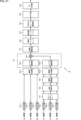
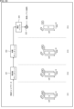
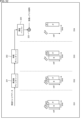
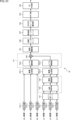
- FIG. 1 illustrates an example of the configuration of a transmission system.
- FIG. 1 is a diagram showing the configuration of a current receiving device.
- FIG. 13 is a diagram showing the delay of a time deinterleaver and a time interleaver, and the required capacity of a delay buffer.
- FIG. 1 is a diagram showing the configuration of a current transmitting device. 1 is a diagram illustrating a first example of a configuration of an embodiment of a transmitting device to which the present disclosure is applied. 1 is a diagram illustrating a first example of a configuration of an embodiment of a receiving device to which the present disclosure is applied.
- FIG. 2 is a diagram illustrating a detailed configuration example of a transmission device to which the present disclosure is applied.
- FIG. 1 is a diagram showing the configuration of a current receiving device.
- FIG. 13 is a diagram showing the delay of a time deinterleaver and a time interleaver, and the required capacity of a delay buffer.
- FIG. 1 is a
- FIG. 11 is a diagram illustrating a second example of a configuration of an embodiment of a transmitting device to which the present disclosure is applied.
- FIG. 11 is a diagram illustrating a second example of a configuration of an embodiment of a receiving device to which the present disclosure is applied.
- FIG. 2 is a diagram illustrating a detailed configuration example of a transmission device to which the present disclosure is applied.
- FIG. 10 is a diagram illustrating a schematic diagram of a process performed by a transmitting device when there is no delay adjustment.
- FIG. 10 is a diagram illustrating the process of a receiving device when there is no delay adjustment.
- FIG. 10 is a diagram illustrating a schematic diagram of a process performed by a transmitting device when delay adjustment is performed.
- FIG. 10 is a diagram illustrating a schematic diagram of a process performed by a transmitting device when delay adjustment is performed.
- FIG. 10 is a diagram illustrating a typical process performed by a receiving device when delay adjustment is performed.
- FIG. 2 is a diagram illustrating a detailed configuration example of a transmission device to which the present disclosure is applied.
- FIG. 13 is a diagram for explaining an example of specifications for hierarchical re-division and delay adjustment.
- FIG. 13 is a diagram for explaining a reduction in the circuitry of a receiving device by adjusting delay in an LL section.
- FIG. 13 is a diagram illustrating a schematic diagram of delay adjustment.
- FIG. 1 is a diagram showing a configuration for performing LDM demodulation processing in a current receiving device. A diagram showing delays in time deinterleaving and time interleaving, and the required capacity of a delay buffer.
- FIG. 1 is a diagram showing a configuration for performing LDM demodulation processing in a current receiving device.
- FIG. 1 is a diagram showing a configuration for performing LDM multiplexing processing in a current transmitting device.
- 1 is a diagram illustrating a first example of a configuration of an embodiment of a transmitting device to which the present disclosure is applied.
- 1 is a diagram illustrating a first example of a configuration of an embodiment of a receiving device to which the present disclosure is applied.
- FIG. 13 is a diagram illustrating another example configuration of a transmission device to which the present disclosure is applied.
- FIG. 11 is a diagram illustrating a second example of a configuration of an embodiment of a transmitting device to which the present disclosure is applied.
- FIG. 11 is a diagram illustrating a second example of a configuration of an embodiment of a receiving device to which the present disclosure is applied.
- FIG. 13 is a diagram illustrating a third example of a configuration of an embodiment of a transmitting device to which the present disclosure is applied.
- 10 is a diagram illustrating a schematic diagram of a process performed by a transmitting device when LL delay adjustment is not performed on the transmitting side.
- FIG. 11 is a diagram illustrating an example of the relationship between a time interleave length and a delay correction amount.
- 10 is a diagram illustrating a schematic diagram of a process performed by a receiving device when LL delay adjustment is not performed on the transmitting side.
- FIG. 1 is a diagram illustrating a schematic diagram of a process performed in a transmitting device when LL delay adjustment is performed on the transmitting side.
- FIG. 13 is a diagram illustrating a schematic diagram of a process performed in a receiving device when LL delay adjustment is performed on the transmitting side.
- FIG. 13 is a diagram illustrating a third example of a configuration of an embodiment of a transmitting device to which the present disclosure is applied.
- FIG. 13 is a diagram illustrating an example of hierarchical reconfiguration by a hierarchical reconfiguration unit.
- 11 is a diagram illustrating an example of LL delay adjustment by a delay adjustment unit. 11 is a diagram for explaining a reduction in the circuitry of a receiving device when LL delay adjustment is performed on the transmitting side.
- FIG. 13 is a flowchart illustrating a flow of a transmission side process.
- 13 is a flowchart illustrating a flow of a receiving side process.
- Fig. 1 is a diagram showing an example of the configuration of a transmission system.
- the transmission system is made up of a transmitting device 10 and a receiving device 20.
- a system refers to a logical collection of multiple devices.
- Transmitting device 10 is a device that transmits content such as broadcast programs and commercials produced by terrestrial broadcasting stations as broadcast signals. Transmitting device 10 generates a broadcast stream, performs the necessary processing, and transmits the resulting terrestrial digital television broadcast signal (hereinafter also referred to as terrestrial broadcast signal) from a transmitting antenna installed at the transmitting station.
- content such as broadcast programs and commercials produced by terrestrial broadcasting stations as broadcast signals.
- Transmitting device 10 generates a broadcast stream, performs the necessary processing, and transmits the resulting terrestrial digital television broadcast signal (hereinafter also referred to as terrestrial broadcast signal) from a transmitting antenna installed at the transmitting station.
- the receiving device 20 is a device capable of receiving broadcast signals from a television receiver, a set-top box (STB), etc.
- the receiving device 20 receives the terrestrial broadcast signal transmitted from the transmitting device 10 via an antenna.
- the receiving device 20 outputs video and audio of content such as a broadcast program by performing the necessary processing on the broadcast stream obtained from the received terrestrial broadcast signal.
- a broadcasting format such as ISDB-T can be used for terrestrial digital television broadcasting.
- ISDB-T is used, but the next generation format for terrestrial digital television broadcasting is under consideration.
- the LDM method as a multiplexing method for broadcast signals to transmit broadcast signals of a new broadcasting method is being considered.
- broadcast signals can be transmitted in a high-power hierarchy as the upper layer (UL: Upper Layer) and a low-power hierarchy as the lower layer (LL: Lower Layer).
- UL high-power hierarchy
- LL Low-power hierarchy
- the high-power hierarchy (UL) will transmit broadcast signals compatible with the existing broadcasting method (ISDB-T)
- the low-power hierarchy (LL) will transmit broadcast signals of a new broadcasting method (the next generation of ISDB-T).
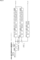
- FIG. 2 is a diagram showing a configuration for performing LDM demodulation processing in a current receiving device, in which the LDM demodulation processing is performed using the successive interference cancellation (SIC) method.
- SIC successive interference cancellation
- the LDM demodulation process in Figure 2 requires multiple time deinterleaving and time interleaving processes.
- the time deinterleaver in the upper row creates a delay of 0 to 380 ms when receiving ISDB-T (UL) and holds 948,480 cells.
- the number of held cells is calculated using the following formula (1).
- "I x (96 - 1)" is the maximum delay of the interleaver
- "I x ((i x 5) mod 96)" is I x mi .
- the time interleaver in the middle (circled number 2) generates a delay of 0 to 380 ms when regenerating ISDB-T (UL) signals, and holds 948,480 cells.
- the delay buffer (circled number 3) is a delay memory for main line data, generates a delay of 380 ms, and holds 1,896,960 cells + ⁇ , where ⁇ represents the delay of the time deinterleaver and anything other than the time interleaver.
- the time deinterleaver in the bottom (circled number 4) generates a delay of 0 to 380 ms when receiving the next-generation system (LL), and holds 948,480 cells.
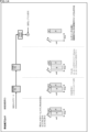
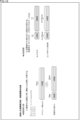
- Figure 3 is a diagram showing the delay of the time deinterleaver and time interleaver in Figure 2, and the required capacity of the delay buffer.
- the circled numbers 1 to 4 correspond to those in Figure 2, and represent the time deinterleaver in the upper row, the time interleaver and delay buffer in the middle row, and the time deinterleaver in the lower row.
- the delay of the time deinterleaver and time interleaver, and the required capacity of the delay buffer can be summarized as follows:
- ISDB-T (UL) reception 0 to 380 ms delay, 948,480 cells
- ISDB-T(UL) signal regeneration 0-380ms delay, 948,480 cells
- Main line data delay memory 380ms delay, 948,480cells x 2
- Next-generation (LL) reception 0 to 380 ms delay, 948,480 cells
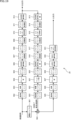
- Fig. 4 shows the configuration for performing LDM modulation processing in current transmitting devices. As shown in Fig. 4, current transmitting devices perform time interleaving on each of the UL and LL signals, and then perform LDM multiplexing.
- current transmission equipment performs LDM multiplexing after time interleaving, which results in increased channel selection time and costs for current reception equipment.
- current transmission equipment has a problem with the way current terrestrial digital broadcast signals and next-generation terrestrial digital broadcast signals are multiplexed, resulting in significant disadvantages in channel selection time and costs on the receiving side.
- this disclosure proposes to improve the channel selection time and cost on the receiving side by performing LDM multiplexing before performing time interleaving (and frequency interleaving) on the transmitting side.
- time interleaving (and frequency interleaving) we propose processing such as hierarchical reconfiguration so that an arbitrary hierarchical structure of LL can accommodate this.
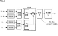
- Fig. 5 is a diagram showing a first example of a configuration of an embodiment of a transmitting device to which the present disclosure is applied.
- Fig. 6 is a diagram showing a first example of a configuration of an embodiment of a receiving device to which the present disclosure is applied.
- the transmitting device of the present disclosure multiplexes (signal multiplexing) the level-adjusted UL signal and the level-adjusted LL signal before performing time interleaving and frequency interleaving. Then, after multiplexing using the LDM method, time interleaving and frequency interleaving are performed.
- the time interleaving length (TIL length) is common to UL and LL.
- the receiving device of the present disclosure when performing LDM demodulation processing using successive interference cancellation (SIC), the receiving device of the present disclosure performs frequency deinterleaving and time deinterleaving before the delay buffer, which makes it possible to reduce the amount of time deinterleaving and time interleaving processing compared to LDM demodulation processing in current receiving devices.
- a delay time of 0 to 380 ms occurs when processing received data, and 948,480 cells are held. The number of held cells is calculated using formula (1) above.
- the delay required to match the replica signal (ISDB-T regenerated signal) for UL cancellation in the LDM system is only a few ms, so the impact on the channel selection time and required capacity of the delay buffer is minimal.
- the receiving device disclosed herein can improve channel selection time and costs.
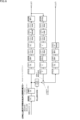
- FIG. 7 is a diagram showing a detailed configuration example of a transmission device to which the present disclosure is applied. As shown in FIG. 7, in the transmission device of the present disclosure, delay adjustment is performed before time interleaving, and OFDM frame construction, IFFT, and GI addition are performed after frequency interleaving.
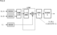
- Fig. 8 is a diagram showing a second example of the configuration of an embodiment of a transmitting device to which the present disclosure is applied.
- Fig. 9 is a diagram showing a second example of the configuration of an embodiment of a receiving device to which the present disclosure is applied.
- the transmitting device of the present disclosure multiplexes (signal multiplexing) the level-adjusted UL signal and the LL signal before performing time interleaving and frequency interleaving. Then, after multiplexing using the LDM method, time interleaving and frequency interleaving are performed.
- the time interleaving length (TIL length) uses the UL setting.
- the LL can have any segment configuration.
- the receiving device of the present disclosure when performing LDM demodulation processing using successive interference cancellation (SIC), performs frequency deinterleaving and time deinterleaving before the delay buffer, thereby reducing the amount of time deinterleaving and time interleaving processing.
- a delay time of 0 to 380 ms occurs and 948,480 cells are held.
- the receiving device disclosed herein can improve tuning time and costs.
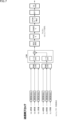
- FIG. 10 is a diagram illustrating a detailed configuration example of a transmission device to which the present disclosure is applied.
- time interleaving time IL
- I delay
- the transmitting device disclosed herein can perform inter-segment IL, hierarchical reconstruction, and delay adjustment processing for LL between BICM and hierarchical synthesis processing.
- inter-segment interleaving is performed individually on the LL for inter-segment IL.
- Inter-segment IL processing is not necessary as it can be performed without it, but having it provides safer performance. In other words, even if there is partial reception on the UL side, inter-segment IL can be achieved only on the LL side.
- This inter-segment IL corresponds to the inter-segment interleaving of the differential modulation section and synchronous modulation section after segment division in current ISDB-T broadcasting.
- the hierarchy allocation is reconfigured from the ABC hierarchy allocation of LL to the ABC hierarchy allocation of UL. This hierarchy reconfiguration process is required.
- time interleaving is performed in the UL hierarchical structure, delay amounts differ at the same hierarchical level. To resolve this, delay adjustment is performed on the transmitting side to ensure that delays are the same at the same hierarchical level. If this delay adjustment is not performed on the transmitting side, it will be necessary to handle it on the receiving side, so it is preferable for it to be performed on the transmitting side. However, it is also acceptable to not perform delay adjustment on the transmitting side and instead perform processing to handle the delay adjustment on the receiving side.
- FIG. 11 is a diagram that shows a schematic of the processing of the transmitting device of the present disclosure without delay adjustment.
- FIG. 12 is a diagram that shows a schematic of the processing of the receiving device of the present disclosure without delay adjustment.
- FIG. 13 is a diagram that shows a schematic diagram of the processing of the transmitting device of the present disclosure when delay adjustment is performed.
- FIG. 14 is a diagram that shows a schematic diagram of the processing of the receiving device of the present disclosure when delay adjustment is performed.
- FIG. 15 is a diagram showing a detailed configuration example of a transmission device to which the present disclosure is applied.
- UL and LL signals are multiplexed before time interleaving and frequency interleaving are performed, and in time interleaving (time IL), the UL setting is used as the time interleaving length (TIL length).
- the transmitting device of the present disclosure can perform inter-segment IL, hierarchical re-division, and delay adjustment processing for the LL between the BICM and hierarchical synthesis processing.
- Example specifications for hierarchical re-division and delay adjustment are shown in FIG. 16.
- the LL hierarchical layer is divided so that it has the same configuration as the UL hierarchical layer.
- delay adjustment a delay is added based on the time interleaving length (TIL length) of each UL hierarchical layer.
- FIG. 17 is a diagram explaining the circuit reduction of the receiving device by adjusting the delay in the LL section.
- FIG. 18 is a diagram showing the delay adjustment of the present disclosure.
- Figure 19 is a diagram showing a configuration for performing LDM demodulation processing in a current receiving device 20.
- the demodulator performs LDM demodulation processing using the successive interference cancellation (SIC) method.
- SIC successive interference cancellation
- the UL hierarchical signal is demodulated from the LDM multiplexed signal, and the demodulated UL hierarchical signal is re-modulated to generate a replica signal, and the replica signal is subtracted from the LDM multiplexed signal to demodulate the LL hierarchical signal.
- the current receiving device 20 holds the signal obtained from the OFDM (Orthogonal Frequency Division Multiplexing) frame received from the current transmitting device 10 (the transmitting device 10 in FIG. 21 described later) in a delay buffer 901 and inputs it to a UL demodulation processing unit that performs UL demodulation processing.
- OFDM Orthogonal Frequency Division Multiplexing
- the UL demodulation processing unit is composed of a frequency deinterleaver 902 that performs frequency deinterleaving, a time deinterleaver 903 that performs time deinterleaving, a demapper unit 904 that performs demapping, a bit deinterleaver 905 that performs bit deinterleaving, an inner code decoding unit 906 that decodes the inner code, a bit-byte conversion unit 907 that performs bit-byte conversion, a byte deinterleaver 908 that performs byte deinterleaving, a byte-bit conversion unit 909 that performs byte-bit conversion, an energy despreading unit 910 that performs energy despreading, a bit-byte conversion unit 911 that performs bit-byte conversion, and an outer code decoding unit 912 that decodes the outer code, and processes the input signal in order.
- the UL layer signal obtained by the UL demodulation processing is output to the subsequent circuit and is also output to the UL remodulation processing
- the UL remodulation processing unit is composed of an outer code encoding unit 913 that performs outer code encoding, a byte-to-bit conversion unit 914 that performs byte-to-bit conversion, an energy diffusion unit 915 that performs energy diffusion, a bit-to-byte conversion unit 916 that performs bit-to-byte conversion, a byte interleaver 917 that performs byte interleaving, a byte-to-bit conversion unit 918 that performs byte-to-bit conversion, an inner code encoding unit 919 that performs inner code encoding, a bit interleaver 920 that performs bit interleaving, a mapping unit 921 that performs mapping, a time interleaver 922 that performs time interleaving, and a frequency interleaver 923 that performs frequency interleaving, and processes the input signal in sequence.
- the replica signal obtained by the UL remodulation processing is output to a subtraction unit 924.
- the subtraction unit 924 receives, in synchronization with each other, the signal delayed by the delay buffer 901 (the LDM multiplexed signal) and a replica signal obtained by demodulating the UL layer signal from the delayed signal and then remodulating it.
- the subtraction unit 924 subtracts the replica signal from the LDM multiplexed signal, and outputs the resulting signal to an LL demodulation processing unit that performs LL demodulation processing.
- the replica signal is a regenerated signal that complies with ISDB-T.
- the LL demodulation processing unit is composed of a frequency deinterleaver 925 that performs frequency deinterleaving, a time deinterleaver 926 that performs time deinterleaving, a demapper unit 927 that performs demapping, a bit deinterleaver 928 that performs bit deinterleaving, an LDPC decoding unit 929 that decodes the LDPC code, a BCH decoding unit 930 that decodes the BCH code, and an energy despreading unit 931 that performs energy despreading, and processes the input signal in order.
- the LL layer signal obtained by the LL demodulation processing is output to the subsequent circuit.
- the current LDM demodulation process in the receiving device 20 involves time deinterleaving by the time deinterleaver 903 and the time deinterleaver 926, and time interleaving by the time interleaver 922, so multiple time deinterleaving and time interleaving processes are required.
- FIG. 20 is a diagram showing the delay in time deinterleaving and time interleaving performed by the receiving device 20 in FIG. 19, and the required capacity of the delay buffer.
- FIG. 20 also shows the transmitting side time interleaving performed by the time interleaver of the current transmitting device 10 (time interleaver 955 in FIG. 21, described later).
- carrier data is represented diagrammatically by boxes in the diagram. In each box in the diagram, D represents carrier data, the superscript number written on D represents the symbol delay, and the subscript number represents the carrier number. Also, the switches in the diagram diagrammatically represent switching between input and output for each carrier.
- the delay buffer 901 performs receiving side delay adjustment
- the time deinterleaver 903 performs receiving side time deinterleaving of the UL demodulation process
- the time interleaver 922 performs receiving side time interleaving of the UL remodulation process
- the subtraction unit 924 subtracts the replica signal from the signal delayed by the delay buffer 901 (the LDM multiplexed signal) to cancel the UL layer signal.
- the receiving side time interleaving by the time interleaver 922 causes a delay of 0 to 380 ms when regenerating the UL layer (ISDB-T) signal, and holds 948,480 cells.
- the delay buffer 901 is a delay memory for main line data (LDM multiplexed signals), and causes a delay of 380 ms, and holds 1,896,960 cells (948,480 cells x 2) + ⁇ , where ⁇ represents the delay excluding receiving side time deinterleaving and receiving side time interleaving.
- the time deinterleaver 926 also performs receiving side time deinterleaving for the LL demodulation process, and this time deinterleaving causes a delay of 0 to 380 ms when receiving the LL layer (next-generation system of ISDB-T), and holds 948,480 cells.
- FIG. 21 is a diagram showing the configuration for performing LDM multiplexing processing in the current transmitting device 10. As shown in FIG. 21, the transmitting device 10 receives three-layer signals (UL signals) of layers A, B, and C as UL layer signals, and three-layer signals (LL signals) of layers A, B, and C as LL layer signals.
- UL signals three-layer signals
- LL signals three-layer signals
- the BICM unit 951-1 performs BICM (Bit Interleaved Coded Modulation) processing on the UL signal of layer A.
- BICM units 951-2 and 951-3 similarly process the UL signals of layers B and C.
- the layer combining unit 953-1 combines the signals of each layer input from the BICM unit 951.
- the combined signal (data carrier symbol) is delayed by a delay adjustment unit 954-1 and input to the time interleaver 955-1.
- the time interleaver 955-1 performs time interleaving (interleaving in the time direction) on the signal after delay adjustment.
- the frequency interleaver 956-1 performs frequency interleaving (interleaving in the frequency direction) on the signal after time interleaving.
- the signal after frequency interleaving is input to the LDM multiplexing unit 971.
- the BICM unit 952-1 performs BICM processing on the LL signal of layer A.
- the BICM units 952-2 and 952-3 process the LL signals of layers B and C.
- the layer combining unit 953-2 combines the signals of each layer input from the BICM unit 952.
- the combined signal (data carrier symbol) is delayed by the delay adjustment unit 954-2 and input to the time interleaver 955-2.
- the time interleaver 955-2 performs time interleaving on the signal after the delay adjustment.
- the frequency interleaver 956-2 performs frequency interleaving on the signal after the time interleaving.
- the signal after the frequency interleaving is input to the LDM multiplexing unit 971.
- the LDM multiplexing unit 971 receives as input the frequency interleaved signal from the frequency interleaver 956-1 (data carrier symbols corresponding to the UL layer signal) and the frequency interleaved signal from the frequency interleaver 956-2 (data carrier symbols corresponding to the LL layer signal).
- the level adjustment unit 957-1 adjusts the power level of the signal after frequency interleaving by the frequency interleaver 956-1
- the level adjustment unit 957-2 adjusts the power level of the signal after frequency interleaving by the frequency interleaver 956-2.
- the multiplexing unit 958 multiplexes the signal input from the level adjustment unit 957-1 (data carrier symbol corresponding to the UL signal) and the signal input from the level adjustment unit 957-2 (data carrier symbol corresponding to the LL signal) using the LDM method, and outputs the multiplexed signal to the OFDM frame construction unit 959.
- the OFDM frame construction unit 959 constructs an OFDM frame by adding a Scattered Pilot (SP) carrier, which is a pilot signal, a Transmission and Multiplexing Configuration and Control (TMCC) carrier, which is transmission control information, and the like, to the data carrier to which the data carrier symbol is assigned, and outputs the frame to the IFFT unit 960.
- SP Scattered Pilot
- TMCC Transmission and Multiplexing Configuration and Control
- the IFFT unit 960 performs an Inverse Fast Fourier Transform (IFFT), and the GI addition unit 961 adds a Guard Interval (GI), thereby OFDM modulating the OFDM frame to generate a transmission signal, which is then transmitted to the outside.
- IFFT Inverse Fast Fourier Transform
- GI Guard Interval
- the UL layer signal (UL signal) and the LL layer signal (LL signal) are each time interleaved separately, and then multiplexed using the LDM method. That is, in the current transmitting device 10, time interleaving is performed by the time interleaver 955, and then LDM multiplexing is performed by the LDM multiplexing unit 971. Therefore, in the current receiving device 20, as shown in FIG. 19, a large number of time deinterleaving and time interleaving processes are required, resulting in increased channel selection time and costs. In other words, in the current transmitting device 10, there is a problem with the way the current terrestrial digital broadcasting signal and the next-generation terrestrial digital broadcasting signal are multiplexed, resulting in significant disadvantages in terms of channel selection time and cost on the receiving side.
- this disclosure proposes to improve the channel selection time and cost on the receiving side by performing LDM multiplexing before performing time interleaving on the transmitting side.
- time interleaving can be performed on the transmitting side that corresponds to the UL hierarchy, and we also propose processing such as hierarchical reconfiguration and delay adjustment so that the LL hierarchy of any hierarchical configuration can correspond to this.
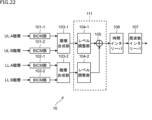
- FIG. 22 is a diagram showing a first example of the configuration of an embodiment of a transmitting device to which the present disclosure is applied.
- two-layer signals (UL signals) of layers A and B are input to the transmitting device 10 as UL layer signals
- two-layer signals (LL signals) of layers A and B are input as LL layer signals.
- the UL layer is a high-power layer in the LDM method.
- the LL layer is a low-power layer in the LDM method.
- Each layer of layers A and B is composed of one or more segments.
- ISDB-T adopts hierarchical transmission in which the transmission bandwidth of one channel is divided into 13 segments for transmission, but it is assumed that the next generation system of ISDB-T will also adopt hierarchical transmission using a multi-segment configuration.
- layers A and B an example of two layers, layers A and B, is shown, but three layers, layers A, B, and C, may be used.
- BICM unit 101-1 performs BICM processing on the UL signal of layer A and outputs the resulting signal to layer combining unit 103-1.
- BICM unit 101-2 processes the UL signal of layer B in the same manner.
- Layer combining unit 103-1 combines the signals (data carrier symbols) of each layer input from BICM unit 101 and outputs the result to LDM multiplexing unit 111.
- BICM unit 102-1 performs BICM processing on the LL signal of layer A and outputs the result to layer combining unit 103-2.
- BICM unit 102-2 processes the LL signal of layer B in the same manner.
- Layer combining unit 103-2 combines the signals (data carrier symbols) of each layer input from BICM unit 102 and outputs the result to LDM multiplexing unit 111.
- the LDM multiplexing unit 111 receives as input the signal from the hierarchical combining unit 103-1 (data carrier symbol corresponding to the UL hierarchical signal) and the signal from the hierarchical combining unit 103-2 (data carrier symbol corresponding to the LL hierarchical signal).
- the level adjustment unit 104-1 adjusts the power level of the signal input from the hierarchical combining unit 103-1
- the level adjustment unit 104-2 adjusts the power level of the signal input from the hierarchical combining unit 103-2.
- the power level is adjusted to multiplex the data carrier symbol corresponding to the UL hierarchical signal and the data carrier symbol corresponding to the LL hierarchical signal by the LDM method.
- the multiplexing unit 105 multiplexes the level-adjusted signal input from the level adjustment unit 104-1 and the level-adjusted signal input from the level adjustment unit 104-2 by the LDM method, and outputs the multiplexed signal to the time interleaver 106.
- the time interleaver 106 performs time interleaving on the multiplexed signal input from the LDM multiplexing unit 111, and outputs the time-interleaved signal to the frequency interleaver 107.
- the frequency interleaver 107 performs frequency interleaving on the time-interleaved signal input from the time interleaver 106, and outputs the frequency-interleaved signal.
- the multiplexing unit 105 before performing time interleaving and frequency interleaving, multiplexes (signal multiplexes) the UL layer signal (UL signal) and the LL layer signal (LL signal) using the LDM method. Then, after multiplexing using the LDM method, time interleaving is performed by the time interleaver 106 and frequency interleaving is performed by the frequency interleaver 107.
- FIG. 23 is a diagram showing a first example of the configuration of an embodiment of a receiving device to which the present disclosure is applied.
- a demodulator performs LDM demodulation processing using successive interference cancellation (SIC) method.
- SIC successive interference cancellation
- the UL layer signal is demodulated from the LDM multiplexed signal, and the demodulated UL layer signal is re-modulated to generate a replica signal, and the LL layer signal is demodulated by subtracting the replica signal from the LDM multiplexed signal.
- SIC successive interference cancellation
- a frequency deinterleaver 201 and a time deinterleaver 202 are provided in front of the delay buffer 203, and when a signal transmitted from the transmitting device 10 of FIG. 22 is received, the carrier data contained in the received signal is input to the frequency deinterleaver 201.
- the frequency deinterleaver 201 performs frequency deinterleaving on the signal input thereto.
- the frequency deinterleaver 201 performs frequency deinterleaving to restore the order of the signals after frequency interleaving by the frequency interleaver 107 in FIG. 22 to the original order.
- the signal after frequency deinterleaving is output to the time deinterleaver 202.
- the time deinterleaver 202 performs time deinterleaving on the frequency deinterleaved signal input from the frequency deinterleaver 201.
- the time deinterleaver 202 performs time deinterleaving to return the order of the signals after time interleaving by the time interleaver 106 in FIG. 22 to the original order.
- the signal after time deinterleaving is held in the delay buffer 203 and is input to a UL demodulation processing unit that performs UL demodulation processing.
- the UL demodulation processing unit is composed of a demapper unit 204 that performs demapping, a bit deinterleaver 205 that performs bit deinterleaving, an inner code decoding unit 206 that decodes the inner code, a bit-byte conversion unit 207 that performs bit-to-byte conversion, a byte deinterleaver 208 that performs byte deinterleaving, a byte-to-bit conversion unit 209 that performs byte-to-bit conversion, an energy despreading unit 210 that performs energy despreading, a bit-to-byte conversion unit 211 that performs bit-to-byte conversion, and an outer code decoding unit 212 that decodes the outer code, and processes the input signal in order.
- the UL layer signal obtained by the UL demodulation processing is output to the subsequent circuit and also to the UL remodulation processing unit that performs the UL remodulation processing.
- the UL remodulation processing unit is composed of an outer code encoding unit 213 that encodes the outer code, a byte-to-bit conversion unit 214 that performs byte-to-bit conversion, an energy diffusion unit 215 that performs energy diffusion, a bit-to-byte conversion unit 216 that performs bit-to-byte conversion, a byte interleaver 217 that performs byte interleaving, a byte-to-bit conversion unit 218 that performs byte-to-bit conversion, an inner code encoding unit 219 that encodes the inner code, a bit interleaver 220 that performs bit interleaving, and a mapping unit 221 that performs mapping, and processes the input signal in sequence.
- the replica signal obtained by the UL remodulation processing is output to a subtraction unit 222.
- the subtraction unit 222 receives, in synchronization with each other, a signal delayed by the delay buffer 203 (the LDM multiplexed signal after time deinterleaving) and a replica signal obtained by demodulating the UL hierarchical signal from the delayed signal and then remodulating it.
- the subtraction unit 222 subtracts the replica signal from the LDM multiplexed signal, and outputs the resulting signal to an LL demodulation processing unit that performs LL demodulation processing.
- the replica signal is a regenerated signal that complies with ISDB-T.
- the LL demodulation processing unit is composed of a demapper unit 223 that performs demapping, a bit deinterleaver 224 that performs bit deinterleaving, an LDPC decoding unit 225 that decodes the LDPC code, a BCH decoding unit 226 that decodes the BCH code, and an energy despreading unit 227 that performs energy despreading, and processes the input signal in order.
- the LL layer signal obtained by the LL demodulation processing is output to the subsequent circuit.
- the receiving device 20 when performing LDM demodulation processing using successive interference cancellation (SIC), the receiving device 20 performs frequency deinterleaving by frequency deinterleaver 201 and time deinterleaving by time deinterleaver 202 before the delay buffer 203. As a result, the receiving device 20 in FIG. 23 can reduce the amount of time deinterleaving and time interleaving compared to the LDM demodulation processing in the receiving device 20 in FIG. 19.
- the UL demodulation processing unit in FIG. 23 does not include a time deinterleaver
- the UL remodulation processing unit in FIG. 23 does not include a time interleaver
- the LL demodulation processing unit in FIG. 23 does not include a time deinterleaver.
- the time deinterleaver 202 in FIG. 23 receives an LDM multiplexed signal, a delay of 0 to 380 ms occurs, and 948,480 cells are held. The number of held cells is calculated using formula (1) above. At this time, the delay required to match the replica signal (ISDB-T regenerated signal) for UL cancellation in the LDM method is only a few ms, so the impact on the channel selection time and required capacity of the delay buffer is minimal. In this way, the receiving device 20 of the present disclosure can improve channel selection time and costs.
- FIG. 24 is a diagram showing another example configuration of a transmitting device to which the present disclosure is applied.
- the transmitting device 10 of FIG. 24 has an additional BICM unit 101-3 and BICM unit 102-3, and also performs BICM processing on the UL and LL signals of layer C, resulting in layer synthesis.
- the transmitting device 10 of FIG. 22 synthesized signals of two layers, layers A and B
- the transmitting device 10 of FIG. 24 synthesizes signals of three layers, layers A, B, and C.
- the transmitting device 10 of FIG. 24 additionally includes a delay adjustment unit 121, an OFDM frame construction unit 122, an IFFT unit 123, and a GI addition unit 124.
- the delay adjustment unit 121 performs delay adjustment on the signal after LDM multiplexing by the LDM multiplexing unit 111, and outputs the resulting signal to the time interleaver 106.
- the time interleaver 106 performs time interleaving on the delayed signal input from the delay adjustment unit 121, and outputs the time-interleaved signal to the frequency interleaver 107.
- the frequency interleaver 107 performs frequency interleaving on the time-interleaved signal input from the time interleaver 106, and outputs the frequency-interleaved signal to the OFDM frame construction unit 122.
- the OFDM frame constructing unit 122 uses the frequency interleaved signal input from the frequency interleaver 107 to construct an OFDM frame by adding an SP carrier, which is a pilot signal, a TMCC carrier, which is transmission control information, and the like, to the data carriers to which the data carrier symbols are assigned, and outputs the frame to the IFFT unit 123.
- the IFFT unit 123 performs IFFT, and the GI adding unit 124 adds a GI, thereby OFDM modulating the OFDM frame to generate a transmission signal, which is then transmitted to the outside.
- the transmitting device 10 of the present disclosure before performing time interleaving, LDM multiplexing of UL layer signals and LL layer signals is performed, and the time interleaving can be performed according to the setting of the time interleaving (UL TIL) of the UL layer. That is, in the transmitting device 10 of the present disclosure, since time interleaving is performed after LDM multiplexing, the time interleaving length (TIL length) is common to the UL layer and the LL layer, but the setting of the UL layer can be used as the time interleaving length (TIL length).
- TIL length time interleaving length
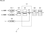
- FIG. 25 is a diagram showing a second example of the configuration of an embodiment of a transmitting device to which the present disclosure is applied. As shown in FIG. 25, two-layer signals (UL signals), A layer and B layer, are input as UL layer signals, and a LL layer signal (LL signal) is input to the transmitting device 10.
- UL signals two-layer signals
- a layer and B layer are input as UL layer signals
- LL signal LL signal
- BICM unit 301-1 performs BICM processing on the UL signal of layer A and outputs the resulting signal to layer combining unit 303.
- BICM unit 301-2 similarly processes the UL signal of layer B.
- Layer combining unit 303 combines the signals of each layer input from BICM unit 301 and outputs the result to LDM multiplexing unit 311.
- BICM unit 302 performs BICM processing on the LL signal and outputs it to LDM multiplexing unit 311.
- the LDM multiplexing unit 311 receives as input the UL layer signal from the layer combining unit 303 and the LL layer signal from the BICM unit 302.
- the level adjustment unit 304 adjusts the power level of the UL layer signal input from the layer combining unit 303 so that it can be multiplexed with the LL layer signal input from the BICM unit 302 using the LDM method.
- the multiplexing unit 305 multiplexes the level-adjusted UL layer signal input from the level adjustment unit 304 and the LL layer signal input from the BICM unit 302 using the LDM method, and outputs the multiplexed signal to the time interleaver 306.
- the time interleaver 306 performs time interleaving on the multiplexed signal input from the LDM multiplexing unit 311.
- the time interleaver 306 performs time interleaving corresponding to the UL layer of the UL and LL layers that are LDM multiplexed, and uses the setting of the UL layer as the time interleave length (TIL length).
- TIL length time interleave length
- the time interleaved signal is output to the frequency interleaver 307.
- the frequency interleaver 307 performs frequency interleaving on the time interleaved signal input from the time interleaver 306, and outputs the frequency interleaved signal.
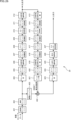
- FIG. 26 is a diagram showing a second example of the configuration of an embodiment of a receiving device to which the present disclosure is applied.
- the receiving device 20 when performing LDM demodulation processing using the successive interference cancellation (SIC) method, frequency deinterleaving and time deinterleaving are performed before the UL demodulation processing, thereby reducing the amount of time deinterleaving and time interleaving processing.
- SIC successive interference cancellation
- a frequency deinterleaver 401 and a time deinterleaver 402 are provided in front of the delay buffer 403, and when a signal transmitted from the transmitting device 10 of FIG. 25 is received, the carrier data contained in the received signal is input to the frequency deinterleaver 401.
- the frequency deinterleaver 401 performs frequency deinterleaving on the signal input thereto.
- the frequency deinterleaver 401 performs frequency deinterleaving to restore the signal order after frequency interleaving by the frequency interleaver 307 in FIG. 25 to the original order.
- the signal after frequency deinterleaving is output to the time deinterleaver 402.
- the time deinterleaver 402 performs time deinterleaving on the frequency deinterleaved signal input from the frequency deinterleaver 401.
- the time deinterleaver 402 performs time deinterleaving to return the order of the signals after time interleaving by the time interleaver 306 in FIG. 25 to the original order.
- the signal after time deinterleaving is held in the delay buffer 403 and is input to the UL demodulation processing unit which performs the UL demodulation process.
- the UL demodulation processing unit like the receiving device 20 in FIG. 23, is composed of a demapper unit 404 to an outer code decoding unit 412, and processes the input signals in sequence.
- the UL layer signal obtained by the UL demodulation processing is output to the subsequent circuit, and is also output to the UL remodulation processing unit which performs UL remodulation processing.
- the UL remodulation processing unit like the receiving device 20 in FIG. 23, is composed of a outer code encoding unit 413 to a mapping unit 421, and processes the input signals in sequence.
- the replica signal obtained by the UL remodulation processing is output to the subtraction unit 422.
- the subtraction unit 422 subtracts the replica signal from the LDM multiplexed signal, and outputs the resulting signal to the LL demodulation processing unit which performs LL demodulation processing.
- the LL demodulation processing unit is composed of the demapper unit 423 to the energy despreading unit 427, similar to the receiving device 20 in FIG. 23, and processes the input signal in order.
- the LL layer signal obtained by the LL demodulation processing is output to the subsequent circuit.
- the transmitting device 10 of the present disclosure can perform LDM multiplexing of the UL layer signal and the LL layer signal, and then perform time interleaving according to the time interleaving settings of the UL layer.
- TIL length time interleaving length
- the delay may be different within the same layer (between segments).
- the transmitting device 10 of the present disclosure can perform inter-segment interleaving, hierarchical reconstruction, and delay adjustment processing for the LL hierarchical signal between the BICM and hierarchical synthesis processing.
- Figure 27 is a diagram showing a third example of the configuration of an embodiment of a transmitting device to which the present disclosure is applied.
- the transmitting device 10 in FIG. 27 is configured by providing an inter-segment interleaver 131, a hierarchy reconstruction unit 132, and a delay adjustment unit 133 between the BICM units 102-1 to 102-3 and the hierarchy synthesis unit 103-2, as compared to the transmitting device 10 in FIG. 24. Therefore, the time interleaver 106 in FIG. 27 performs time interleaving according to the setting of the time interleaving (UL TIL) of the UL hierarchy.
- UL TIL time interleaving
- the former delay adjustment is also referred to as pre-TIL delay adjustment
- the latter delay adjustment is also referred to as LL delay adjustment.
- the inter-segment interleaver 131 performs inter-segment interleaving on the signals of each layer of the LL layer that has been subjected to BICM processing, and outputs the resulting signal to the layer reconstruction unit 132.
- inter-segment interleaving is not performed on partial reception, so inter-segment interleaving is performed individually on the LL layer.
- the hierarchical reconfiguration unit 132 performs hierarchical reconfiguration on the signals of each layer input from the inter-segment interleaver 131, and outputs the resulting hierarchically reconfigured signals of each layer to the delay adjustment unit 133.
- time interleaving is performed after multiplexing using the LDM method, so hierarchical reconfiguration is performed before hierarchical synthesis of the LL layer.
- the delay adjustment unit 133 performs LL delay adjustment on the signals of each layer input from the layer reconfiguration unit 132, and outputs the resulting delay-adjusted signals of each layer to the layer synthesis unit 103-2.
- hierarchical reconfiguration of the LL layer is performed to perform time interleaving in the hierarchical configuration of the UL layer, but for the LL layer, the delay amount is different within the same layer (between segments) before the reconfiguration.
- LL delay adjustment is performed to eliminate the state in which the delay amount is different within the same layer (between segments) of the LL layer, and to make the delay amount the same within the same layer (between segments).
- inter-segment interleaver 131 In the transmitting device 10 of FIG. 27, it is of course possible to provide all of the inter-segment interleaver 131, hierarchical reconstruction unit 132, and delay adjustment unit 133, but it is not necessary to provide all of them, and only some of them may be provided.
- performance is improved by implementing inter-segment interleaving, it is possible to achieve the system without implementing it, so the inter-segment interleaver 131 does not have to be a required component.
- performance can be improved by implementing inter-segment interleaving only on the LL layer side.
- inter-segment interleaving by the inter-segment interleaver 131 corresponds to the inter-segment interleaving of the differential modulation unit and synchronous modulation unit after segment division as specified in ISDB-T.
- Hierarchical reconfiguration is a necessary process when following the time interleaving settings of the UL hierarchy, and the hierarchy reconfiguration unit 132 can be a necessary component. If LL delay adjustment is not performed on the transmitting side, it will be necessary to handle it on the receiving side, so it is expected that it will be performed by the transmitting device 10 on the transmitting side. However, it is also possible that the transmitting device 10 on the transmitting side does not perform LL delay adjustment, and the receiving device 20 on the receiving side performs processing corresponding to the LL delay adjustment.
- Fig. 28 is a diagram showing a schematic diagram of the process performed by the transmitting device 10 in the case where the transmitting side does not perform LL delay adjustment.
- the transmitting device 10 in FIG. 28 does not perform LL delay adjustment, and therefore the delay adjustment unit 133 has been removed.
- the signals processed in each block are represented diagrammatically by boxes D1 to D9 separated by vertical dashed lines corresponding to the input and output of each block.
- the boxes represent the time direction on the X axis, the direction in which the cells are arranged (frequency direction) on the Y axis, and the power direction on the Z axis.
- D1 to D5 represent UL layer signals before LDM multiplexing in the upper boxes, and LL layer signals in the lower boxes. Boxes D6 to D9 represent signals after LDM multiplexing.
- the "A” in the top box represents tier A and the “B” represents tier B, indicating that the UL tier is composed of 13 segments, consisting of 1 segment in tier A (UL A) and 12 segments in tier B (UL B).
- the "A" in the bottom box represents tier A, and indicates that the LL tier is composed of the 13 segments in tier A.
- the signal processed by the BICM unit 102 is subjected to inter-segment interleaving by the inter-segment interleaver 131 and hierarchical reconfiguration by the hierarchy reconfiguration unit 132, and the resulting signal is processed by the hierarchy synthesis unit 103-2.
- level adjustment units 104-1 and 104-2 perform level adjustment
- multiplexing unit 105 multiplexes the level-adjusted signals, so that the boxes corresponding to the 13 segments of the UL layer and the boxes corresponding to the 13 segments of the LL layer are overlapped in the power direction (D6).
- the delay adjustment unit 121 performs pre-TIL delay adjustment on the LDM multiplexed signal.
- Figure 29 shows an example of the relationship between the time interleave length and the amount of delay correction.
- the time interleave length is specified by I, an independent parameter for each layer, and for delay time differences that occur between layers, the transmitter corrects the delay by the number of symbols shown in Figure 29 so that the total transmission and reception delay is an integer multiple of a frame.
- I the TIL length of layer A
- UL B the TIL length of layer B
- a delay of 1 frame and 14 symbols is added using the relationship shown in Figure 29.
- time interleaving is performed by time interleaver 106 (D8).
- This time interleaving is performed according to the settings of the time interleaving of the UL hierarchy (UL TIL).
- Frequency interleaving is performed by frequency interleaver 107 on the signal after time interleaving (D9). Note that in reality, a symbol delay is added for each cell, but this is not shown in the figure to simplify the explanation.
- Fig. 30 is a diagram showing a schematic diagram of the processing performed by the receiving device 20 when LL delay adjustment is not performed on the transmitting side.
- the signals processed in the blocks at the previous stage in the receiving device 20 of Fig. 23 are shown diagrammatically by the boxes D11 to D14 separated by vertical dashed lines corresponding to the input and output of each block.
- the transmitting device 10 in FIG. 28 transmits a signal that has been subjected to pre-TIL delay adjustment to the receiving device 20 in FIG. 30 (D11).
- the frequency deinterleaver 201 performs frequency deinterleaving on the signal (carrier data) received from the transmitting device 10, but this is omitted from the illustration here due to rearrangement in the frequency direction (D12).
- the time deinterleaver 202 performs time deinterleaving on the signal after frequency deinterleaving.
- the time deinterleaver 202 in FIG. 30 performs time deinterleaving to return the signal order after time interleaving by the time interleaver 106 in FIG. 28 to the original order.
- a delay of four frames is applied to the A layer of the UL layer (UL A) in a total of four frames for transmission and reception
- a delay of two frames is applied to the B layer of the UL layer (UL B) in a total of two frames for transmission and reception (D13).
- the subtraction unit 222 subtracts the replica signal from the time deinterleaved signal held in the delay buffer 203, and the signal of the A layer of the LL layer is demodulated using the resulting signal, but the delay according to the time deinterleaving remains even after the UL layer signal is cancelled (D14).
- the transmitting device 10 on the transmitting side does not perform LL delay adjustment, even after the UL layer signal is canceled using the replica signal, a delay corresponding to time deinterleaving is added, so in order to demodulate the LL layer signal, the receiving device 20 on the receiving side must perform processing to adjust the delay.
- Fig. 31 is a diagram showing a schematic diagram of a process performed by the transmitting device 10 when implementing LL delay adjustment on the transmitting side.
- the transmitting device 10 in FIG. 31 is provided with a delay adjustment unit 133 to perform LL delay adjustment.
- signals processed in the preceding blocks are represented diagrammatically by boxes D21 to D29 separated by vertical dashed lines corresponding to the inputs and outputs of each block.
- Inter-segment interleaving and hierarchical reconstruction are the same as in FIG. 28 (D22, D23).
- the delay adjustment unit 133 performs LL delay adjustment on the signals of each layer of the LL layer input from the layer reconfiguration unit 132. That is, the hierarchical reconfiguration of the LL layer is performed to perform time interleaving in the hierarchical configuration of the UL layer, but for the LL layer, the delay amount is different within the same layer (between segments) before the reconfiguration.
- LL delay adjustment is performed so that the delay amount is the same within the same layer (between segments) (D24).
- delay adjustment may be performed based on the time interleaving length (TIL length) of the UL hierarchical layer to match the maximum delay, so that the amount of delay is the same between segments in the same hierarchical layer. More specifically, as shown in FIG.
- level adjustment units 104-1 and 104-2 perform level adjustment
- multiplexing unit 105 multiplexes the level-adjusted signals, so that the boxes corresponding to the 13 segments of the UL layer and the boxes corresponding to the 13 segments of the LL layer are overlapped in the power direction (D25, D26).
- the delay adjustment unit 121 performs pre-TIL delay adjustment on the LDM multiplexed signal (D27). For example, using the relationship shown in Figure 29, it is possible to add a delay of 2 frames and 28 symbols to layer A and a delay of 1 frame and 14 symbols to layer B.
- a delay of 2 frames and 28 symbols is added to layer A, and a delay of 1 frame and 14 symbols is added to layer B (D27).
- a delay of 2 frames and 28 symbols is added to the part of the UL layer corresponding to layer A, and a delay of 1 frame and 14 symbols is added to the part of the UL layer corresponding to layer B (D27).
- a pre-TIL delay adjustment is further performed by delay adjustment unit 121 (D27).
- time interleaving is performed by the time interleaver 106.
- This time interleaving is performed according to the settings of the time interleaving of the UL hierarchy (UL TIL).
- UL TIL the time interleaving of the UL hierarchy
- the frequency interleaving of the signal after time interleaving is performed by the frequency interleaver 107 (D29).
- Fig. 32 is a diagram showing a schematic diagram of the processing performed by the receiving device 20 when LL delay adjustment is performed on the transmitting side.
- the signals processed in the blocks at the previous stage in the receiving device 20 of Fig. 23 are shown diagrammatically by the boxes D31 to D34 separated by vertical dashed lines corresponding to the input and output of each block.
- the transmitting device 10 in FIG. 31 transmits a signal that has been subjected to LL delay adjustment and pre-TIL delay adjustment to the receiving device 20 in FIG. 32 (D31).
- the frequency deinterleaver 201 performs frequency deinterleaving on the signal (carrier data) received from the transmitting device 10, but this is omitted from the illustration here due to rearrangement in the frequency direction (D32).
- the time deinterleaver 202 performs time deinterleaving on the signal after frequency deinterleaving.
- the time deinterleaver 202 in FIG. 32 performs time deinterleaving to return the order of the signals after time interleaving by the time interleaver 106 in FIG. 31 to the original order.
- a delay of four frames in total for transmission and reception is applied to the A layer of the UL layer (UL A), and a delay of two frames in total for transmission and reception is applied to the B layer of the UL layer (UL B) (D33).
- the subtraction unit 222 subtracts the replica signal from the time deinterleaved signal held in the delay buffer 203, and the signal at the A layer of the LL layer is demodulated using the resulting signal.
- the delay adjustment unit 133 on the transmitting side performs LL delay adjustment for the LL layer to match the maximum delay based on the time interleaving length (TIL length) of the UL layer, the delay is canceled after time deinterleaving by the time deinterleaver 202 on the receiving side.
- TIL length time interleaving length
- Fig. 33 is a diagram showing a third example of the configuration of an embodiment of a transmitting device to which the present disclosure is applied.
- the transmitting device 10 in Fig. 33 is configured similarly to the transmitting device 10 in Fig. 27, but Fig. 33 will be described with particular attention to the processing performed by the hierarchical reconfiguration unit 132 and the delay adjustment unit 133.
- the hierarchy reconfiguration unit 132 in FIG. 33 reconfigures (re-splits) the LL hierarchy so that it has the same configuration as the UL hierarchy.
- the hierarchy reconfiguration the hierarchy allocation is reconfigured so that the allocation of the A, B, and C hierarchies in the LL hierarchy is the same as the allocation of the A, B, and C hierarchies in the UL hierarchy.
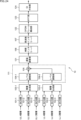
- the UL hierarchy is composed of 13 segments, consisting of 1 segment in the A hierarchical layer (UL A) and 12 segments in the B hierarchical layer (UL B), as shown in FIG. 34
- the hierarchy reconfiguration unit 132 splits the 13 segments in the A hierarchical layer of the LL hierarchy into 1 segment and 12 segments, just like the UL hierarchy.
- the delay adjustment unit 133 in Figure 33 adjusts the delay of each layer in the LL hierarchy after the hierarchy reconfiguration.
- the delay adjustment unit 133 adds a delay amount equivalent to 0 frames based on the TIL length of tier A (UL A) of the UL hierarchy to 1 segment (LL A 1Seg) of tier A of the LL hierarchy after the hierarchy reconfiguration, and adds a delay amount equivalent to 2 frames based on the TIL length of tier B (UL B) of the UL hierarchy to 12 segments (LL A 12Seg) of tier A of the LL hierarchy after the hierarchy reconfiguration.
- the delay amount is calculated from "maximum delay amount - delay amount of each hierarchy".
- the delay amount for 1 segment (LL A 1Seg) in tier A of the LL tier after hierarchical reconfiguration is 4 frames
- no delay adjustment is required for 1 segment (LL A 1Seg) in tier A of the LL tier.
- the delay amount for 12 segment (LL A 12Seg) in tier A of the LL tier after hierarchical reconfiguration is 2 frames
- a delay adjustment of 2 frames is performed for 12 segment (LL A 12Seg) in tier A of the LL tier.
- the UL layer signal and the LL layer signal are multiplexed before time interleaving is performed, but when performing time interleaving, if the UL layer setting is used as the time interleaving length (TIL length), LL delay adjustment is performed in the LL layer after layer reconfiguration.
- TIL length time interleaving length
- LL demodulation processing can be performed on the 13-segment LL layer signal.
- FIG. 36 is a diagram explaining the circuit reduction of the receiving device 20 when LL delay adjustment is performed on the transmitting side.
- signals processed by the transmitting device 10 carrier data after LL hierarchy re-division by the hierarchy reconfiguration unit 132, after LL delay adjustment by the delay adjustment unit 133, after pre-TIL delay adjustment by the delay adjustment unit 121, and after time interleaving (TIL) by the time interleaver 106 are represented diagrammatically by squares in the figure.
- TIL time interleaving
- D represents carrier data
- the superscript number next to D represents the symbol delay
- the subscript number represents the carrier number.
- the squares with a dotted pattern represent carrier data in layer B
- the squares without a pattern represent carrier data in layer A.
- time interleaving is performed by the time interleaver 106, and then an OFDM frame is constructed and transmitted via the transmission path.
- the OFDM frame transmitted via the transmission path is received, and time deinterleaving is performed by the time deinterleaver 202.
- TDIL time deinterleaving
- the carrier data at layer A of the UL hierarchy UL A
- the carrier data at layer B of the UL hierarchy UL B
- the carrier data at layer A of the UL hierarchy has a symbol delay of 816 symbols (dashed line frame L in the figure).
- the symbol delay of one segment of layer A of the LL layer (LL A 1Seg) is 816 symbols (436 symbols + 380 symbols), and the symbol delay of 12 segments of layer A of the LL layer (LL A 12Seg) is 816 symbols (626 symbols + 190 symbols), so the number of symbol delays in the LL layer are the same. Therefore, the receiving device 20 does not need a buffer to match the symbol delays, resulting in a reduction in circuitry.
- FIG. 37 is a flowchart illustrating the flow of the transmission side process executed by the transmitting device 10 shown in FIG. 22, FIG. 24, etc.
- step S11 the BICM unit 101 and the hierarchy synthesis unit 103-1 perform UL processing corresponding to the UL hierarchy.
- step S12 the BICM unit 102 and the hierarchy synthesis unit 103-2 perform LL processing corresponding to the LL hierarchy.
- step S13 the LDM multiplexing unit 111 multiplexes the signal obtained by the UL processing and the signal obtained by the LL processing using the LDM method.
- step S14 the time interleaver 106 performs time interleaving on the LDM multiplexed signal.
- the frequency interleaver 107 performs frequency interleaving on the time interleaved signal.
- step S16 the OFDM frame constructor 122 constructs an OFDM frame using the frequency interleaved signal.
- the layer reconfiguration unit 132 may reconfigure the LL layer. Also, when the delay adjustment unit 121 performs pre-TIL delay adjustment, the delay adjustment unit 133 performs LL delay adjustment, so that the receiving side does not need a buffer to match the symbol delay.
- FIG. 38 is a flowchart illustrating the flow of the receiving side process executed by the receiving device 20 of FIG. 23 etc.
- the receiving device 20 receives the OFDM frame transmitted from the transmitting device 10 (S31) and executes the processes from step S32 onwards.
- the frequency deinterleaver 201 performs frequency deinterleaving on the signal obtained from the received OFDM frame.
- the time deinterleaver 202 performs time deinterleaving on the signal after frequency deinterleaving.
- a UL demodulation processing unit such as the demapper unit 204 performs UL demodulation processing using the signal after time deinterleaving.
- the UL layer signal obtained by the UL demodulation processing is output to the outside and also to the UL remodulation processing unit.
- a UL remodulation processing unit such as the outer code encoding unit 213 performs UL remodulation processing using the UL layer signal after UL demodulation.
- step S36 an LL demodulation processing unit such as the demapper unit 223 performs LL demodulation processing using the signal obtained by subtracting the replica signal from the signal before UL demodulation.
- the signal of the LL layer obtained by the LL demodulation process is output to the outside.
- the transmitting device A signal of a first layer, which is a high-power layer in an LDM system, is multiplexed with a signal of a second layer, which is a low-power layer in the LDM system; After multiplexing, the signal is time interleaved.
- the transmission method according to (2) further comprising multiplexing a signal of the first layer and a signal of the second layer after layer reconfiguration.
- the transmission method according to (3) further comprising: performing delay adjustment according to the time interleaving on the signal of the second layer after hierarchical reconfiguration and before multiplexing.
- frequency interleaving is performed.
- a multiplexing unit that multiplexes a signal of a first layer, which is a high-power layer in an LDM system, and a signal of a second layer, which is a low-power layer in the LDM system; a time interleaver that performs time interleaving on the multiplexed signal; A frame constructing unit that constructs an OFDM frame using the time-interleaved signal.
- a multiplexing unit that multiplexes a signal of a first layer, which is a high-power layer in an LDM system, and a signal of a second layer, which is a low-power layer in the LDM system; a time interleaver that performs time interleaving on the multiplexed signal; a frame constructing unit that constructs an OFDM frame using the time-interleaved signal; and a time deinterleaver that performs time deinterleaving to return the sequence of the time-interleaved signals obtained from the OFDM frame transmitted from a transmitting device including the time-interleaved signal to the original sequence;
- a receiving device comprising: a demodulation unit that demodulates the first layer signal and the second layer signal using a time-deinterleaved signal.
- the transmitting device further includes a frequency interleaver that performs frequency interleaving on the time-interleaved signal, and the frame constructing unit constructs the OFDM frame using the frequency-interleaved signal;
- the OFDM frame may further include a frequency deinterleaver that performs frequency deinterleaving to return a signal sequence after frequency interleaving to an original sequence,
- the receiving device according to (7), wherein the time deinterleaver performs the time deinterleaving on a signal that has been frequency deinterleaved.
- the time-deinterleaved signal is stored in a delay buffer.
- the receiving device further comprising: a signal obtained by subtracting the replica signal from the time-deinterleaved signal stored in the delay buffer, the signal of the second layer being demodulated.
- the receiving device a multiplexing unit that multiplexes a signal of a first layer, which is a high-power layer in an LDM system, and a signal of a second layer, which is a low-power layer in the LDM system; a time interleaver that performs time interleaving on the multiplexed signal; a frame constructing unit that constructs an OFDM frame using the time-interleaved signal; and A receiving method comprising: demodulating the first layer signal and the second layer signal using a time-deinterleaved signal.
Landscapes
- Engineering & Computer Science (AREA)
- Signal Processing (AREA)
- Computer Networks & Wireless Communication (AREA)
- Detection And Prevention Of Errors In Transmission (AREA)
Abstract
Description
図1は、伝送システムの構成例を示す図である。図1において、伝送システムは、送信装置10と、受信装置20から構成される。システムとは、複数の装置が論理的に集合したものをいう。
図2は、現状の受信装置におけるLDM復調処理を行う構成を示す図である。図2では、逐次干渉除去(SIC:Successive Interference Cancellation)法を用いたLDM復調処理が行われる。

ISDB-T(UL)信号再生成:0~380ms遅延、948,480cell
本線データの遅延メモリ:380ms遅延、948,480cell×2
次世代方式(LL)受信:0~380ms遅延、948,480cell
図5は、本開示を適用した送信装置の一実施の形態の構成の第1の例を示す図である。図6は、本開示を適用した受信装置の一実施の形態の構成の第1の例を示す図である。
図8は、本開示を適用した送信装置の一実施の形態の構成の第2の例を示す図である。図9は、本開示を適用した受信装置の一実施の形態の構成の第2の例を示す図である。
図10は、本開示を適用した送信装置の詳細な構成例を示す図である。
図19乃至図21を参照して、現状のLDM方式での問題点について説明する。図19は、現状の受信装置20におけるLDM復調処理を行う構成を示す図である。

図22は、本開示を適用した送信装置の一実施の形態の構成の第1の例を示す図である。図22に示すように、送信装置10には、UL階層の信号として、A階層、B階層の2階層の信号(UL信号)が入力され、LL階層の信号として、A階層、B階層の2階層の信号(LL信号)が入力される。UL階層は、LDM方式における高電力階層となる層である。LL階層は、LDM方式における低電力階層となる層である。A階層、B階層の各階層は、1以上のセグメントから構成される。例えば、ISDB-Tでは1チャンネルの伝送帯域幅を13個のセグメントに分割して伝送する階層伝送を採用しているが、ISDB-Tの次世代方式でも複数セグメント構成を用いた階層伝送の採用が想定される。ここでは、A,B階層の2階層の例を示しているが、A,B,C階層の3階層であってもよい。
本開示の送信装置10では、時間インタリーブを行う前に、UL階層の信号とLL階層の信号とのLDM多重化を行うが、時間インタリーブは、UL階層の時間インタリーブ(UL TIL)の設定に従って実施することができる。すなわち、本開示の送信装置10では、LDM多重化の後に時間インタリーブを行うため、時間インタリーブ長(TIL長)は、UL階層とLL階層で共通化されるが、時間インタリーブ長(TIL長)としてUL階層の設定を用いることができる。
本開示の送信装置10では、時間インタリーブを行う前に、UL階層の信号とLL階層の信号とのLDM多重化を行うが、時間インタリーブは、UL階層の時間インタリーブの設定に従って実施することができる。UL階層の時間インタリーブの設定に従う場合、UL階層の階層ごとに、時間インタリーブ長(TIL長)が異なる可能性がある。このとき、LL階層にとっては、同一階層内(のセグメント間)で遅延が異なる状態となる可能性がある。
図28乃至図30を参照して、送信側でLL遅延調整を実施しない場合の構成を説明する。ただし、説明の簡略化のために、時間方向に注目して説明をし、周波数方向の詳細については適宜省略する。図28は、送信側でLL遅延調整を実施しない場合に送信装置10で行われる処理を模式的に示した図である。
図31、図32を参照して、送信側でLL遅延調整を実施する場合の構成を説明する。図31は、送信側でLL遅延調整を実施する場合に送信装置10で行われる処理を模式的に示した図である。
図33は、本開示を適用した送信装置の一実施の形態の構成の第3の例を示す図である。図33の送信装置10は、図27の送信装置10と同様に構成されるが、図33では、特に、階層再構成部132と遅延調整部133で行われる処理に注目して説明する。
図37は、図22、図24等の送信装置10により実行される送信側処理の流れを説明するフローチャートである。
図38は、図23等の受信装置20により実行される受信側処理の流れを説明するフローチャートである。
送信装置が、
LDM方式における高電力階層となる第1の階層の信号と、前記LDM方式における低電力階層となる第2の階層の信号とを多重化し、
多重化後の信号に対し、時間インタリーブを行い、
時間インタリーブ後の信号を用いて、OFDMフレームを構成する
送信方法。
(2)
前記時間インタリーブは、前記第1の階層に対応した時間インタリーブである
前記(1)に記載の送信方法。
(3)
前記第2の階層を、前記第1の階層に対応するように再構成する階層再構成を行い、
前記第1の階層の信号と、階層再構成後の前記第2の階層の信号とを多重化する
前記(2)に記載の送信方法。
(4)
階層再構成後の前記第2の階層の信号であって多重化前の信号に対し、前記時間インタリーブに応じた遅延調整を行う
前記(3)に記載の送信方法。
(5)
時間インタリーブ後の信号に対し、周波数インタリーブを行い、
周波数インタリーブ後の信号を用いて、前記OFDMフレームを構成する
前記(1)乃至(4)のいずれかに記載の送信方法。
(6)
LDM方式における高電力階層となる第1の階層の信号と、前記LDM方式における低電力階層となる第2の階層の信号とを多重化する多重化部と、
多重化後の信号に対し、時間インタリーブを行う時間インタリーバと、
時間インタリーブ後の信号を用いて、OFDMフレームを構成するフレーム構成部と
を備える送信装置。
(7)
LDM方式における高電力階層となる第1の階層の信号と、前記LDM方式における低電力階層となる第2の階層の信号とを多重化する多重化部と、
多重化後の信号に対し、時間インタリーブを行う時間インタリーバと、
時間インタリーブ後の信号を用いて、OFDMフレームを構成するフレーム構成部と
を備える送信装置から送信されてくる前記OFDMフレームから得られる、前記時間インタリーブ後の信号の並びを、元の並びに戻す時間デインタリーブを行う時間デインタリーバと、
時間デインタリーブ後の信号を用いて、前記第1の階層の信号と前記第2の階層の信号の復調を行う復調部と
を備える受信装置。
(8)
前記送信装置は、時間インタリーブ後の信号に対し、周波数インタリーブを行う周波数インタリーバをさらに備え、前記フレーム構成部は、周波数インタリーブ後の信号を用いて、前記OFDMフレームを構成しており、
前記OFDMフレームから得られる、周波数インタリーブ後の信号の並びを、元の並びに戻す周波数デインタリーブを行う周波数デインタリーバをさらに備え、
前記時間デインタリーバは、周波数デインタリーブ後の信号に対し、前記時間デインタリーブを行う
前記(7)に記載の受信装置。
(9)
時間デインタリーブ後の信号を遅延バッファに保持し、
時間デインタリーブ後の信号を用いて、前記第1の階層の信号を復調し、
復調した前記第1の階層の信号を再変調してレプリカ信号を生成し、
前記遅延バッファに保持した時間デインタリーブ後の信号から、前記レプリカ信号を減じて得られる信号を用いて、前記第2の階層の信号を復調する
前記(7)又は(8)に記載の受信装置。
(10)
受信装置が、
LDM方式における高電力階層となる第1の階層の信号と、前記LDM方式における低電力階層となる第2の階層の信号とを多重化する多重化部と、
多重化後の信号に対し、時間インタリーブを行う時間インタリーバと、
時間インタリーブ後の信号を用いて、OFDMフレームを構成するフレーム構成部と
を備える送信装置から送信されてくる前記OFDMフレームから得られる、前記時間インタリーブ後の信号の並びを、元の並びに戻す時間デインタリーブを行い、
時間デインタリーブ後の信号を用いて、前記第1の階層の信号と前記第2の階層の信号の復調を行う
受信方法。
Claims (10)
- 送信装置が、
LDM方式における高電力階層となる第1の階層の信号と、前記LDM方式における低電力階層となる第2の階層の信号とを多重化し、
多重化後の信号に対し、時間インタリーブを行い、
時間インタリーブ後の信号を用いて、OFDMフレームを構成する
送信方法。 - 前記時間インタリーブは、前記第1の階層に対応した時間インタリーブである
請求項1に記載の送信方法。 - 前記第2の階層を、前記第1の階層に対応するように再構成する階層再構成を行い、
前記第1の階層の信号と、階層再構成後の前記第2の階層の信号とを多重化する
請求項2に記載の送信方法。 - 階層再構成後の前記第2の階層の信号であって多重化前の信号に対し、前記時間インタリーブに応じた遅延調整を行う
請求項3に記載の送信方法。 - 時間インタリーブ後の信号に対し、周波数インタリーブを行い、
周波数インタリーブ後の信号を用いて、前記OFDMフレームを構成する
請求項1に記載の送信方法。 - LDM方式における高電力階層となる第1の階層の信号と、前記LDM方式における低電力階層となる第2の階層の信号とを多重化する多重化部と、
多重化後の信号に対し、時間インタリーブを行う時間インタリーバと、
時間インタリーブ後の信号を用いて、OFDMフレームを構成するフレーム構成部と
を備える送信装置。 - LDM方式における高電力階層となる第1の階層の信号と、前記LDM方式における低電力階層となる第2の階層の信号とを多重化する多重化部と、
多重化後の信号に対し、時間インタリーブを行う時間インタリーバと、
時間インタリーブ後の信号を用いて、OFDMフレームを構成するフレーム構成部と
を備える送信装置から送信されてくる前記OFDMフレームから得られる、前記時間インタリーブ後の信号の並びを、元の並びに戻す時間デインタリーブを行う時間デインタリーバと、
時間デインタリーブ後の信号を用いて、前記第1の階層の信号と前記第2の階層の信号の復調を行う復調部と
を備える受信装置。 - 前記送信装置は、時間インタリーブ後の信号に対し、周波数インタリーブを行う周波数インタリーバをさらに備え、前記フレーム構成部は、周波数インタリーブ後の信号を用いて、前記OFDMフレームを構成しており、
前記OFDMフレームから得られる、周波数インタリーブ後の信号の並びを、元の並びに戻す周波数デインタリーブを行う周波数デインタリーバをさらに備え、
前記時間デインタリーバは、周波数デインタリーブ後の信号に対し、前記時間デインタリーブを行う
請求項7に記載の受信装置。 - 時間デインタリーブ後の信号を遅延バッファに保持し、
時間デインタリーブ後の信号を用いて、前記第1の階層の信号を復調し、
復調した前記第1の階層の信号を再変調してレプリカ信号を生成し、
前記遅延バッファに保持した時間デインタリーブ後の信号から、前記レプリカ信号を減じて得られる信号を用いて、前記第2の階層の信号を復調する
請求項7に記載の受信装置。 - 受信装置が、
LDM方式における高電力階層となる第1の階層の信号と、前記LDM方式における低電力階層となる第2の階層の信号とを多重化する多重化部と、
多重化後の信号に対し、時間インタリーブを行う時間インタリーバと、
時間インタリーブ後の信号を用いて、OFDMフレームを構成するフレーム構成部と
を備える送信装置から送信されてくる前記OFDMフレームから得られる、前記時間インタリーブ後の信号の並びを、元の並びに戻す時間デインタリーブを行い、
時間デインタリーブ後の信号を用いて、前記第1の階層の信号と前記第2の階層の信号の復調を行う
受信方法。
Priority Applications (1)
| Application Number | Priority Date | Filing Date | Title |
|---|---|---|---|
| JP2024554467A JPWO2024095907A1 (ja) | 2022-10-31 | 2023-10-27 |
Applications Claiming Priority (2)
| Application Number | Priority Date | Filing Date | Title |
|---|---|---|---|
| JP2022-174579 | 2022-10-31 | ||
| JP2022174579 | 2022-10-31 |
Publications (1)
| Publication Number | Publication Date |
|---|---|
| WO2024095907A1 true WO2024095907A1 (ja) | 2024-05-10 |
Family
ID=90930464
Family Applications (1)
| Application Number | Title | Priority Date | Filing Date |
|---|---|---|---|
| PCT/JP2023/038830 Ceased WO2024095907A1 (ja) | 2022-10-31 | 2023-10-27 | 送信方法、送信装置、受信装置、及び受信方法 |
Country Status (2)
| Country | Link |
|---|---|
| JP (1) | JPWO2024095907A1 (ja) |
| WO (1) | WO2024095907A1 (ja) |
Citations (3)
| Publication number | Priority date | Publication date | Assignee | Title |
|---|---|---|---|---|
| JP2020014036A (ja) * | 2018-07-13 | 2020-01-23 | マクセル株式会社 | デジタル放送変調波の伝送方法 |
| JP2020096230A (ja) * | 2018-12-10 | 2020-06-18 | ソニー株式会社 | 送信装置、送信方法、受信装置、及び受信方法 |
| US20200396110A1 (en) * | 2019-06-17 | 2020-12-17 | Electronics And Telecommunications Research Institute | Modulation and demodulation method in layer-division multiplexing system, and receiver thereof |
-
2023
- 2023-10-27 JP JP2024554467A patent/JPWO2024095907A1/ja active Pending
- 2023-10-27 WO PCT/JP2023/038830 patent/WO2024095907A1/ja not_active Ceased
Patent Citations (3)
| Publication number | Priority date | Publication date | Assignee | Title |
|---|---|---|---|---|
| JP2020014036A (ja) * | 2018-07-13 | 2020-01-23 | マクセル株式会社 | デジタル放送変調波の伝送方法 |
| JP2020096230A (ja) * | 2018-12-10 | 2020-06-18 | ソニー株式会社 | 送信装置、送信方法、受信装置、及び受信方法 |
| US20200396110A1 (en) * | 2019-06-17 | 2020-12-17 | Electronics And Telecommunications Research Institute | Modulation and demodulation method in layer-division multiplexing system, and receiver thereof |
Also Published As
| Publication number | Publication date |
|---|---|
| JPWO2024095907A1 (ja) | 2024-05-10 |
Similar Documents
| Publication | Publication Date | Title |
|---|---|---|
| US9979498B2 (en) | Broadcast-signal transmitter/receiver and method for transmitting/receiving broadcast signals | |
| KR101921178B1 (ko) | 방송 신호 송/수신기 및 방송 신호 송/수신 방법 | |
| KR101844229B1 (ko) | 방송 신호 송/수신기 및 방송 신호 송/수신 방법 | |
| KR101079106B1 (ko) | 신호 송수신 장치 및 신호 송수신 방법 | |
| CN102783111B (zh) | 发射机和发送方法 | |
| JP6346274B2 (ja) | 放送信号送信装置、放送信号受信装置、放送信号送信方法及び放送信号受信方法 | |
| JP6174788B2 (ja) | 放送信号送信装置、放送信号受信装置、放送信号送信方法及び放送信号受信方法 | |
| DK2536133T3 (en) | Method and apparatus for receiving a transmission signal | |
| EP3529962A1 (en) | Transmitter, receiver, transmitting method, and receiving method | |
| JP2020184666A (ja) | 送信装置及びプログラム | |
| DK2536132T3 (en) | Method for sending a transmission signal and apparatus thereof | |
| GB2515892A (en) | Transmission techniques | |
| JP7453825B2 (ja) | 送信装置および受信装置 | |
| WO2024095907A1 (ja) | 送信方法、送信装置、受信装置、及び受信方法 | |
| KR102461179B1 (ko) | 송신 장치, 수신 장치 및 그 제어 방법 | |
| BR112013008868B1 (pt) | Receptor, receptor de televisão, e, método de recepção e recuperação de símbolos de dados de serviço local | |
| JP7847255B2 (ja) | 送信装置および受信装置 | |
| JP2024062695A (ja) | 送信装置及び受信装置 | |
| JP7798631B2 (ja) | 送信装置およびプログラム | |
| JP7723565B2 (ja) | 送信装置、受信装置、及び中継局 | |
| JP7267378B2 (ja) | 送信装置、及び受信装置 | |
| JP7128657B2 (ja) | 送信装置、受信装置、送受信システム、及びチップ | |
| WO2024106194A1 (ja) | 送信装置、送信方法、受信装置、及び受信方法 | |
| Posega | Advanced OFDM systems for terrestrial multimedia links | |
| KR20110068806A (ko) | 티디엠비 시스템의 계층변조 방법, 계층복조 방법 및 이를 지원하는 송수신기 |
Legal Events
| Date | Code | Title | Description |
|---|---|---|---|
| 121 | Ep: the epo has been informed by wipo that ep was designated in this application |
Ref document number: 23885663 Country of ref document: EP Kind code of ref document: A1 |
|
| WWE | Wipo information: entry into national phase |
Ref document number: 2024554467 Country of ref document: JP |
|
| NENP | Non-entry into the national phase |
Ref country code: DE |
|
| REG | Reference to national code |
Ref country code: BR Ref legal event code: B01A Ref document number: 112025007871 Country of ref document: BR |
|
| 122 | Ep: pct application non-entry in european phase |
Ref document number: 23885663 Country of ref document: EP Kind code of ref document: A1 |
|
| ENP | Entry into the national phase |
Ref document number: 112025007871 Country of ref document: BR Kind code of ref document: A2 Effective date: 20250422 |