WO2024095705A1 - 電力変換装置、プログラム - Google Patents
電力変換装置、プログラム Download PDFInfo
- Publication number
- WO2024095705A1 WO2024095705A1 PCT/JP2023/036600 JP2023036600W WO2024095705A1 WO 2024095705 A1 WO2024095705 A1 WO 2024095705A1 JP 2023036600 W JP2023036600 W JP 2023036600W WO 2024095705 A1 WO2024095705 A1 WO 2024095705A1
- Authority
- WO
- WIPO (PCT)
- Prior art keywords
- terminal
- potential side
- arm switch
- switch
- lower arm
- Prior art date
- Legal status (The legal status is an assumption and is not a legal conclusion. Google has not performed a legal analysis and makes no representation as to the accuracy of the status listed.)
- Ceased
Links
Images








Classifications
-
- H—ELECTRICITY
- H02—GENERATION; CONVERSION OR DISTRIBUTION OF ELECTRIC POWER
- H02M—APPARATUS FOR CONVERSION BETWEEN AC AND AC, BETWEEN AC AND DC, OR BETWEEN DC AND DC, AND FOR USE WITH MAINS OR SIMILAR POWER SUPPLY SYSTEMS; CONVERSION OF DC OR AC INPUT POWER INTO SURGE OUTPUT POWER; CONTROL OR REGULATION THEREOF
- H02M1/00—Details of apparatus for conversion
- H02M1/14—Arrangements for reducing ripples from DC input or output
-
- H—ELECTRICITY
- H02—GENERATION; CONVERSION OR DISTRIBUTION OF ELECTRIC POWER
- H02M—APPARATUS FOR CONVERSION BETWEEN AC AND AC, BETWEEN AC AND DC, OR BETWEEN DC AND DC, AND FOR USE WITH MAINS OR SIMILAR POWER SUPPLY SYSTEMS; CONVERSION OF DC OR AC INPUT POWER INTO SURGE OUTPUT POWER; CONTROL OR REGULATION THEREOF
- H02M7/00—Conversion of AC power input into DC power output; Conversion of DC power input into AC power output
- H02M7/02—Conversion of AC power input into DC power output without possibility of reversal
- H02M7/04—Conversion of AC power input into DC power output without possibility of reversal by static converters
- H02M7/12—Conversion of AC power input into DC power output without possibility of reversal by static converters using discharge tubes with control electrode or semiconductor devices with control electrode
Definitions
- This disclosure relates to a power conversion device and a program.
- a power conversion device compatible with both three-phase AC power supplies and single-phase AC power supplies.
- This power conversion device includes a series connection of upper and lower arm switches for three phases, a series connection of upper and lower arm diodes, a high-potential side path, a low-potential side path, and a DC side capacitor.
- the high-potential side path electrically connects the high-potential side terminals of each upper arm switch, the cathodes of the upper arm diodes, the high-potential side terminal of the capacitor, and the high-potential side DC terminal.
- the low-potential side path electrically connects the low-potential side terminals of each lower arm switch, the anodes of the lower arm diodes, the low-potential side terminal of the capacitor, and the low-potential side DC terminal.
- the power conversion device further includes first to third inductors.
- the first inductor electrically connects the connection point of the first upper and lower arm switches to a first AC terminal
- the second inductor electrically connects the connection point of the second upper and lower arm switches to a second AC terminal
- the third inductor electrically connects the connection point of the third upper and lower arm switches to a third AC terminal.
- the power conversion device includes a connection path that electrically connects the connection points of the upper and lower arm diodes and a fourth AC terminal, a first switch provided in the connection path, a second switch that electrically connects the first AC terminal and the second AC terminal, and a third switch that electrically connects the second AC terminal and the third AC terminal.
- the power conversion device When a three-phase AC power supply is connected to the first AC terminal, the second AC terminal, and the third AC terminal, the power conversion device performs switching control of the upper and lower arm switches to convert the AC power input from the first AC terminal, the second AC terminal, and the third AC terminal into DC power and output it from the high potential side DC terminal and the low potential side DC terminal when the first to third switches are in an OFF state.
- the power conversion device when a single-phase AC power supply is connected to the first AC terminal and the fourth AC terminal, the power conversion device performs switching control of the upper and lower arm switches in order to convert the AC power input from the first AC terminal and the fourth AC terminal into DC power and output it from the high potential side DC terminal and the low potential side DC terminal with the first to third switches turned on. Because the second and third switches are turned on, all of the first to third inductors can be used as power transmission paths during power conversion using a single-phase AC power supply. This makes it possible to increase the DC power output from the high potential side DC terminal and the low potential side DC terminal.
- the primary objective of this disclosure is to provide a power conversion device and program that can increase the DC power output while reducing DC power pulsation during power conversion using a single-phase AC power source.
- the present disclosure provides a power supply comprising a first AC terminal, a second AC terminal, a third AC terminal, and a fourth AC terminal; A high potential side DC terminal and a low potential side DC terminal; Equipped with A power conversion device configured to be connectable to the first AC terminal, the second AC terminal, and the third AC terminal, and configured to be connectable to the first AC terminal and the fourth AC terminal, a series connection of a first upper arm switch and a first lower arm switch; a series connection of a second upper arm switch and a second lower arm switch; a third upper arm switch and a third lower arm switch connected in series; A series connection of an upper arm rectifier and a lower arm rectifier; a high potential side path electrically connecting the high potential side terminals of the first, second and third upper arm switches, the high potential side terminal of the upper arm rectifier unit, and the high potential side DC terminal; a low potential side path electrically connecting the low potential side terminals of the first, second and third lower arm switches, the low potential side terminal of the lower arm rectifier unit,
- the second single-phase charging switch is turned on, and the first and second inductors can be used as a power transmission path. This makes it possible to increase the DC power output from the high-potential side DC terminal and the low-potential side DC terminal.
- the compensation switch is turned on, and the high potential side path or the low potential side path is electrically connected to the third AC terminal via the compensation storage unit.
- the compensation storage unit can charge and discharge an electric charge to absorb the pulsation of the DC power.
- the control unit performs switching control of the third upper arm switch and the third lower arm switch to reduce the pulsation of the DC power output from the high potential side DC terminal and the low potential side DC terminal due to the charging and discharging of the compensation storage unit.
- the pulsation of the DC power can be reduced while increasing the output DC power.
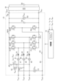
- FIG. 1 is an overall configuration diagram of an on-board charger according to a first embodiment
- FIG. 2 is a diagram showing an on-board charger connected to a three-phase AC power supply
- FIG. 3 is a diagram showing an on-board charger connected to a single-phase AC power source
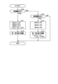
- FIG. 4 is a flowchart showing a procedure for controlling charging of a storage battery.
- FIG. 5 is a block diagram of a three-phase charging control process
- FIG. 6 is a time chart showing the transition of current, voltage, etc. during three-phase charging control.
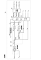
- FIG. 7 is a block diagram of a single-phase charging control process
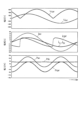
- FIG. 8 is a time chart showing the transition of current, voltage, etc. during single-phase charging control.
- FIG. 9 is a time chart relating to a pulsation reduction process according to the second embodiment.
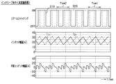
- FIG. 10 is a time chart showing interleaved driving according to the third embodiment;
- FIG. 11 is a time chart showing a switching mode etc. according to a comparative example.
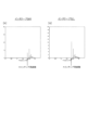
- FIG. 12 shows the results of FFT analysis showing the effect of reducing the current ripple.
- FIG. 13 is an overall configuration diagram of an on-board charger according to another embodiment;
- FIG. 14 is a diagram showing the overall configuration of an on-board charger according to another embodiment.
- the power conversion device according to this embodiment is provided in a vehicle such as an electric vehicle, and specifically, is an AC-DC-DC converter constituting an on-board charger.
- the on-board charger is also called an on-board charger.
- the power conversion device has an AC terminal and a DC terminal.
- the power conversion device has a function of converting AC power input via the AC terminal connected to an AC power source outside the vehicle into DC power and outputting it from the DC terminal.
- the DC power output from the DC terminal is supplied to a storage battery provided in the vehicle.
- the power conversion device also has a function of converting DC power input from the DC terminal into AC power and outputting it from the AC terminal.
- the AC power output from the AC terminal is supplied to an external power system via an external AC power source.
- the power conversion device can be connected to a three-phase AC power source or a single-phase AC power source.
- the power conversion device 10 has a first AC terminal Tac1, a second AC terminal Tac2, a third AC terminal Tac3, and a fourth AC terminal Tac4 as AC terminals.
- the first to fourth AC terminals Tac1 to Tac4 can be connected to an external three-phase AC power source 21 as shown in FIG. 2.
- the first and fourth AC terminals Tac1 and Tac4 can be connected to an external single-phase AC power source 22 as shown in FIG. 3.
- the power conversion device 10 has a high-potential side DC terminal TdcH and a low-potential side DC terminal TdcL as DC terminals.
- the high-potential side DC terminal TdcH and the low-potential side DC terminal TdcL are connected to the input section of a DCDC converter 24 constituting an on-board charger.
- the output section of the DCDC converter 24 is connected to a chargeable and dischargeable storage battery 20 mounted on the vehicle.
- the DCDC converter 24 transforms the DC voltage input from the high-potential side DC terminal TdcH and the low-potential side DC terminal TdcL, and supplies the transformed DC voltage to the storage battery 20.
- the DCDC converter 24 also transforms the DC voltage input from the storage battery 20 and supplies it to the high-potential side DC terminal TdcH and the low-potential side DC terminal TdcL.
- the DCDC converter 24 is, for example, an insulated DCDC converter in which the input section and the output section are electrically insulated, and includes a transformer that connects the input section and the output section.
- the power conversion device 10 includes four upper and lower arm switches for four phases, which are a series connection of a first upper arm switch S1H and a first lower arm switch S1L, a series connection of a second upper arm switch S2H and a second lower arm switch S2L, a series connection of a third upper arm switch S3H and a third lower arm switch S3L, and a series connection of a fourth upper arm switch S4H and a fourth lower arm switch S4L.
- each of the upper and lower arm switches S1H to S4L is an N-channel MOSFET having a body diode. Therefore, in each of the upper and lower arm switches S1H to S4L, the high potential side terminal is the drain, and the low potential side terminal is the source.
- the first phase is the U phase
- the second phase is the V phase
- the third phase is the W phase.
- the fourth upper arm switch S4H corresponds to the "upper arm rectifier”
- the fourth lower arm switch S4L corresponds to the "lower arm rectifier”.
- the power conversion device 10 includes a high-potential side path 30H, which is an electrical path connecting the high-potential side terminals of the first, second, third, and fourth upper arm switches S1H, S2H, S3H, and S4H to the high-potential side DC terminal TdcH, and a low-potential side path 30L, which is an electrical path connecting the low-potential side terminals of the first, second, third, and fourth lower arm switches S1L, S2L, S3L, and S4L to the low-potential side DC terminal TdcL.
- the high-potential side path 30H and the low-potential side path 30L are conductive members such as bus bars.
- the power conversion device 10 includes a DC side capacitor 34 that connects the high potential side path 30H and the low potential side path 30L.
- the DC side capacitor 34 functions as a smoothing capacitor and is, for example, an electrolytic capacitor.
- the power conversion device 10 includes a first path 41, a second path 42, and a third path 43.
- the first path 41 is an electrical path that connects the low potential side terminal of the first upper arm switch S1H and the high potential side terminal of the first lower arm switch S1L to the first AC terminal Tac1.
- the second path 42 is an electrical path that connects the low potential side terminal of the second upper arm switch S2H and the high potential side terminal of the second lower arm switch S2L to the second AC terminal Tac2.
- the third path 43 is an electrical path that connects the low potential side terminal of the third upper arm switch S3H and the high potential side terminal of the third lower arm switch S3L to the third AC terminal Tac3.
- the power conversion device 10 includes a first inductor 31 provided in a first path 41, a second inductor 32 provided in a second path 42, and a third inductor 33 provided in a third path 43.
- the inductors 31 to 33 have the same specifications. Therefore, the inductance values of the inductors 31 to 33 are the same.
- the rated currents (specifically, the temperature rise rated currents) of the inductors 31 to 33 are the same.
- the power conversion device 10 includes a connection path 44, which is an electrical path that connects the low potential side terminal of the fourth upper arm switch S4H and the high potential side terminal of the fourth lower arm switch S4L to the fourth AC terminal Tac4.
- the power conversion device 10 includes a first single-phase charging switch 45 provided on the connection path 44.
- the first single-phase charging switch 45 allows bidirectional current flow when it is turned on, and prevents bidirectional current flow when it is turned off.
- the power conversion device 10 includes a second single-phase charging switch 46.
- the second single-phase charging switch 46 connects a portion of the first path 41 closer to the first AC terminal Tac1 than the first inductor 31 and a portion of the second path 42 closer to the second AC terminal Tac2 than the second inductor 32.
- the second single-phase charging switch 46 allows bidirectional current flow when it is turned on, and blocks bidirectional current flow when it is turned off.
- the second single-phase charging switch 46 may, for example, connect the first AC terminal Tac1 and the second AC terminal Tac2.
- the power conversion device 10 includes a series connection of a compensation capacitor 47 and a compensation switch 48 as a configuration for reducing pulsation of the DC power output from each of the DC terminals TdcH and TdcL.
- the series connection of the compensation capacitor 47 and the compensation switch 48 connects the high potential side path 30H and a portion of the third path 43 closer to the third AC terminal Tac3 than the third inductor 33.
- the compensation capacitor 47 is, for example, a film capacitor.
- the compensation switch 48 allows bidirectional current flow when it is turned on, and blocks bidirectional current flow when it is turned off.
- the series connection of the compensation capacitor 47 and the compensation switch 48 may connect the high potential side path 30H and the third AC terminal Tac3.
- the compensation capacitor 47 may be provided on the high potential side path 30H side than the compensation switch 48.
- the power conversion device 10 includes a DC side voltage sensor 50, an AC side voltage sensor 51, and a compensation voltage sensor 52.
- the DC side voltage sensor 50 detects the terminal voltage of the DC side capacitor 34
- the AC side voltage sensor 51 detects the voltage difference between the first AC terminal Tac1 and the fourth AC terminal Tac4
- the compensation voltage sensor 52 detects the terminal voltage of the compensation capacitor 47.
- the power conversion device 10 is equipped with first to third current sensors 61 to 63.
- the first current sensor 61 detects the current flowing through the first inductor 31
- the second current sensor 62 detects the current flowing through the second inductor 32
- the third current sensor 63 detects the current flowing through the third inductor 33.
- the detection values of each of the sensors 50 to 52, 61 to 63 are input to a control device 70, which serves as a control unit provided in the power conversion device 10.
- the control device 70 is mainly composed of a microcomputer 71, which has a CPU.
- the functions provided by the microcomputer 71 can be provided by software recorded in a physical memory device and a computer that executes the software, by software alone, by hardware alone, or by a combination of these.
- the microcomputer 71 when the microcomputer 71 is provided by an electronic circuit that is hardware, it can be provided by a digital circuit including a large number of logic circuits, or by an analog circuit.
- the microcomputer 71 executes a program stored in a non-transitory tangible storage medium that serves as a storage unit provided in the microcomputer 71.
- the program includes, for example, programs for the processes shown in Figures 4, 5, 7, etc., which will be described later.
- the storage unit is, for example, a non-volatile memory.
- the programs stored in the storage unit can be updated via a communication network such as the Internet, for example, OTA (Over The Air), etc.
- the control device 70 performs three-phase charging control or single-phase charging control.
- the charging control is explained below using the flowchart in Figure 4.
- step S10 it is determined whether or not an instruction for three-phase charging control has been issued.
- a three-phase AC power supply 21 is connected to the first to third AC terminals Tac1 to Tac3
- an instruction for three-phase charging control has been issued.
- the amplitude and frequency of the output voltage of the three phases are the same, and the phases of the output voltage and output current are shifted by 120° for each phase.
- the neutral point of the three-phase AC power supply 21 is connected to the fourth AC terminal Tac4, but the neutral point does not have to be connected to the fourth AC terminal Tac4.
- step S10 three-phase charging control is performed in steps S11 and S12. More specifically, in step S11, the first single-phase charging switch 45, the second single-phase charging switch 46, and the compensation switch 48 are turned off. In addition, the fourth upper arm switch S4H and the fourth lower arm switch S4L are turned off.
- step S12 the first, second and third upper arm switches S1H, S2H and S3H and the first, second and third lower arm switches S1L, S2L and S3L are switched on alternately with dead time between them, so that the AC power input from the first AC terminal Tac1, the second AC terminal Tac2 and the third AC terminal Tac3 is converted into DC power and output from the high potential side DC terminal TdcH and the low potential side DC terminal TdcL.
- the upper arm switches and the lower arm switches are alternately turned on with dead time between them. In each phase, one switching period of the upper and lower arm switches is the same.
- step S10 determines whether or not a command for single-phase charging control has been issued.
- the amplitude of the output voltage of the single-phase AC power supply 22 is the same as the amplitude of the output voltage of the three-phase AC power supply 21.
- the frequency of the output voltage of the single-phase AC power supply 22 is the same as the frequency of the output voltage of the three-phase AC power supply 21.
- step S13 single-phase charging control is performed in steps S14 and S15. More specifically, in step S14, the first single-phase charging switch 45, the second single-phase charging switch 46, and the compensation switch 48 are turned on.
- step S15 the first upper arm switch S1H, the first lower arm switch S1L, the second upper arm switch S2H, and the second lower arm switch S2L are switched on in order to convert the AC power input from the first AC terminal Tac1 and the fourth AC terminal Tac4 into DC power and output it from the high potential side DC terminal TdcH and the low potential side DC terminal TdcL.
- the upper arm switch and the lower arm switch are alternately turned on in synchronization with each other with a dead time in between.
- one switching period of the upper and lower arm switches is the same, and is the same as one switching period during three-phase charging control.
- switching control is performed on the third upper arm switch S3H and the third lower arm switch S3L.
- the third upper arm switch S3H and the third lower arm switch S3L are alternately turned on with dead time in between.
- the third upper and lower arm switches S3H and S3L have the same switching period, which is also the same as the first and second upper and lower arm switches S1H, S1L, S2H, S2L.
- step S15 in a first period in which a current flows from the fourth AC terminal Tac4 to the first AC terminal Tac1 via the single-phase AC power supply 22, the fourth lower arm switch S4L is turned on and the fourth upper arm switch S4H is turned off.
- the fourth upper arm switch S4H is turned on and the fourth lower arm switch S4L is turned off. Whether the current timing is included in the first period or the second period may be determined based on, for example, the detection value of the first current sensor 61.
- One switching period Tsw4 of the fourth upper and lower arm switches S4H and S4L is the same as one period of the output voltage of the single-phase AC power supply 22, and is longer than one switching period Tsw1, Tsw2, and Tsw3 of the first, second, and third upper and lower arm switches S1H, S1L, S2H, S2L, S3H, and S3L.
- the fourth upper and lower arm switches S4H and S4L are semiconductor switching elements with longer turn-on and turn-off times than the first to third upper and lower arm switches S1H, S1L, S2H, S2L, S3H, and S3L. This eliminates the need to use high-performance switches for the fourth upper and lower arm switches S4H and S4L, reducing the cost of the power conversion device 10.
- step S15 during a first period in which a current flows from the fourth AC terminal Tac4 to the first AC terminal Tac1 via the single-phase AC power source 22, the fourth upper arm switch S4H is turned on and the fourth lower arm switch S4L is turned off.
- FIG. 5 is a block diagram of the three-phase charging control executed by the control device 70.
- the voltage control unit 80 calculates the d-axis target current Idref for controlling the terminal voltage of the DC side capacitor 34 detected by the DC side voltage sensor 50 (hereinafter, the DC voltage detection value Vdcr) to the target DC voltage Vdcref.
- the voltage control unit 80 includes a voltage deviation calculation unit 81 and a voltage feedback control unit 82.
- the voltage deviation calculation unit 81 calculates the voltage deviation ⁇ V by subtracting the DC voltage detection value Vdcr from the target DC voltage Vdcref.
- the target DC voltage Vdcref may be set, for example, based on the rated voltages of the upper and lower arm switches S1H to S4L and the DCDC converter 24.
- the voltage feedback control unit 82 calculates the d-axis target current Idref as a manipulated variable for feedback-controlling the voltage deviation ⁇ V to 0.
- the feedback control in the voltage feedback control unit 82 is, for example, proportional-integral control.
- the electrical angle calculation unit 83 calculates the electrical angle ⁇ e based on the voltage detected by the AC side voltage sensor 51 (hereinafter, AC voltage detection value V1r).
- the electrical angle ⁇ e at the zero-cross timing (specifically, for example, the zero-upcross timing) of the AC voltage detection value V1r is set to 0°, and the electrical angle ⁇ e at the next zero-upcross timing is set to 360°.
- one cycle of the AC voltage detection value V1r corresponds to one electrical angle cycle (0° to 360°).
- the AC voltage detection value V1r is set to positive when the voltage of the first AC terminal Tac1 is higher than the voltage of the fourth AC terminal Tac4.
- the two-phase conversion unit 84 converts the first, second, and third current detection values i1r, i2r, and i3r in the three-phase fixed coordinate system into d- and q-axis currents Idr and Iqr in the two-phase rotating coordinate system (dq-axis coordinate system) based on the currents detected by the first, second, and third current sensors 61, 62, and 63 (hereinafter referred to as the first, second, and third current detection values i1r, i2r, and i3r) and the electrical angle ⁇ e.
- the first, second, and third current detection values i1r, i2r, and i3r are positive when they flow from the first, second, and third AC terminals Tac1, Tac2, and Tac3 toward the first, second, and third inductors 31, 32, and 33.
- the current control unit 85 includes a d-axis deviation calculation unit 86, a d-axis feedback control unit 87, a q-axis deviation calculation unit 88, and a q-axis feedback control unit 89.
- the d-axis deviation calculation unit 86 calculates the d-axis current deviation ⁇ Id by subtracting the d-axis current Idr from the d-axis target current Idref.
- the d-axis feedback control unit 87 calculates the d-axis target voltage Vdref as a manipulated variable for feedback controlling the d-axis current deviation ⁇ Id to zero.
- the feedback control in the d-axis feedback control unit 87 is, for example, proportional-integral control.
- the q-axis deviation calculation unit 88 calculates the q-axis current deviation ⁇ Iq by subtracting the q-axis current Iqr from the q-axis target current Iqref.
- the q-axis target current Iqref is a target value of the reactive current, and in this embodiment, is set to 0 to make the power factor 1.
- Making the power factor 1 means making the phase difference between the first, second, and third output voltages V1, V2, and V3 of the three-phase AC power supply 21 and the first, second, and third current detection values i1r, i2r, and i3r 0.
- the q-axis feedback control unit 89 calculates the q-axis target voltage Vqref as a manipulated variable for feedback controlling the q-axis current deviation ⁇ Iq to 0.
- the feedback control in the q-axis feedback control unit 89 is, for example, proportional-integral control.
- the three-phase conversion unit 90 converts the d- and q-axis target voltages Vdref, Vqref in the two-phase rotating coordinate system into first, second, and third target voltages Vleg1ref, Vleg2ref, and Vleg3ref in the three-phase fixed coordinate system based on the d- and q-axis target voltages Vdref, Vqref and the electrical angle ⁇ e.
- the first, second, and third target voltages Vleg1ref, Vleg2ref, and Vleg3ref are sinusoidal signals whose phases are shifted by 120° in electrical angle.
- the sinusoidal signals are signals that become 0 every 180° of electrical angle.
- the PWM generating unit 91 generates a first upper and lower arm drive signal to be supplied to the gates of the first upper and lower arm switches S1H and S1L, a second upper and lower arm drive signal to be supplied to the gates of the second upper and lower arm switches S2H and S2L, and a third upper and lower arm drive signal to be supplied to the gates of the third upper and lower arm switches S3H and S3L by pulse width modulation (PWM) based on a comparison of the magnitude of the first, second and third target voltages Vleg1ref, Vleg2ref, Vleg3ref with the carrier signal.
- the carrier signal is, for example, a triangular wave signal, and one cycle of the carrier signal is sufficiently shorter than one electrical angle cycle (0° to 360°).
- the switching patterns of the first upper and lower arm switches S1H and S1L, the switching patterns of the second upper and lower arm switches S2H and S2L, and the switching patterns of the third upper and lower arm switches S3H and S3L are shifted in phase by 120°.
- Fig. 6 shows the transition of the first, second, and third output voltages V1, V2, and V3 of the three-phase AC power supply 21, the first, second, and third current detection values i1r, i2r, and i3r, the total value of the first, second, and third DC powers P1, P2, and P3, and the DC power Pdc output from each DC terminal TdcH and TdcL during three-phase charging control.
- the first, second, and third output voltages V1, V2, and V3 are positive when the voltages of the first, second, and third AC terminals Tac1, Tac2, and Tac3 are higher than the voltage of the neutral point of the three-phase AC power supply 21.
- the first, second, and third DC powers P1, P2, and P3 are individual DC powers output from the three-phase AC power supply 21 through the first, second, and third inductors 31, 32, and 33 from each DC terminal TdcH and TdcL.
- the frequency of the output voltages V1 to V3 of the three-phase AC power supply 21 is 50 Hz, and the target DC voltage Vdcref is set to 800 V.
- three-phase charging control is performed so that the phase difference between the first, second, and third output voltages V1, V2, and V3 and the first, second, and third current detection values i1r, i2r, and i3r is 0 (i.e., the power factor is 1).
- the first, second, and third target voltages Vleg1ref, Vleg2ref, and Vleg3ref are calculated in the three-phase conversion unit 90 so that the first DC power P1, the second DC power P2, and the third DC power P3 are equal.
- the effective value of the current flowing through the first, second, and third inductors 31, 32, and 33 is 16 Arms.
- control device 70 may perform three-phase charging control by performing switching control of the upper and lower arm switches S1H to S3L of the first to third phases based on average current mode control or the like, instead of the control shown in FIG. 5.
- FIG. 7 is a block diagram of the single-phase charging control executed by the control device 70.
- the control device 70 includes a charging control unit 100 for power transmission and a pulsation reduction control unit 120 for reducing pulsation in the DC power.
- the filter unit 112 performs low-pass filtering on the DC voltage detection value Vdcr. This removes the harmonic components of the output voltage of the single-phase AC power supply 22 that are included in the DC voltage detection value Vdcr.
- the harmonic components are, for example, components of the secondary frequency of the output voltage (for example, 100 Hz or 120 Hz).
- the voltage control unit 101 includes a voltage deviation calculation unit 102 and a voltage feedback control unit 103.
- the voltage deviation calculation unit 102 calculates a voltage deviation ⁇ V by subtracting the DC voltage detection value Vdcr from the target DC voltage Vdcref from which harmonic components have been removed in the filter unit 112.
- the voltage feedback control unit 103 calculates a target current amplitude Iampref as a manipulated variable for feedback controlling the voltage deviation ⁇ V to 0.
- the feedback control in the voltage feedback control unit 103 is, for example, proportional-integral control.
- the electrical angle calculation unit 83 calculates the electrical angle ⁇ e based on the AC voltage detection value V1r.
- the sine wave generation unit 109 generates a sine wave signal "sin ⁇ e" based on the electrical angle ⁇ e.
- the current control unit 105 includes a target current calculation unit 106, a current deviation calculation unit 107, and a current feedback control unit 108.
- the target current calculation unit 106 calculates the target current Iacref by multiplying the target current amplitude Iampref by the sine wave signal "sin x ⁇ e".
- the target current Iacref fluctuates with the same period as the AC voltage detection value V1r.
- the current deviation calculation unit 107 calculates the current deviation ⁇ I by subtracting the sum of the first current detection value i1r and the second current detection value i2r from the target current Iacref. The sum of the first current detection value i1r and the second current detection value i2r is calculated in the current addition unit 110.
- the current feedback control unit 108 calculates the first and second target voltages Vleg1ref, Vleg2ref as manipulated variables for feedback control of the current deviation ⁇ I to zero.
- the feedback control in the current feedback control unit 108 is, for example, proportional-integral control.
- the first and second target voltages Vleg1ref, Vleg2ref are signals of the same phase.
- the first and second target voltages Vleg1ref, Vleg2ref are calculated in the current feedback control unit 108 so that the first DC power P1 and the second DC power P2 are equal.
- the first PWM generating unit 111 generates a first upper and lower arm drive signal to be supplied to the gates of the first upper and lower arm switches S1H and S1L and a second upper and lower arm drive signal to be supplied to the gates of the second upper and lower arm switches S2H and S2L by pulse width modulation based on a magnitude comparison between the first and second target voltages Vleg1ref and Vleg2ref and the carrier signal.
- the phase difference between the switching pattern of the first upper and lower arm switches S1H and S1L and the switching pattern of the second upper and lower arm switches S2H and S2L is 0°.
- the on-switching timing and off-switching timing of the first upper arm switch S1H and the second upper arm switch S2H are synchronized, and the on-switching timing and off-switching timing of the first lower arm switch S1L and the second lower arm switch S2L are synchronized.
- the maximum value of the DC power output from the high potential side DC terminal TdcH and the low potential side DC terminal TdcL is Pdcmax.
- the charging control unit 100 generates the first upper and lower arm drive signal and the second upper and lower arm drive signal so that the maximum value of the DC power output from the high potential side DC terminal TdcH and the low potential side DC terminal TdcL in single-phase charging control is Pdcmax ⁇ 2/3 or less.
- the voltage feedback control unit 103 calculates the target current amplitude Iampref so that the maximum value of the DC power output from the high potential side DC terminal TdcH and the low potential side DC terminal TdcL in single-phase charging control is Pdcmax ⁇ 2/3 or less.
- the maximum current flowing through the first and second inductors 31, 32 during single-phase charging control to be equal to or less than the maximum current flowing through the first and second inductors 31, 32 during three-phase charging control.
- the rated current specifically, the temperature rise rated current
- the first, second, and third inductors 31, 32, and 33 can be reduced, allowing the first, second, and third inductors 31, 32, and 33 to be made smaller.
- the target compensation voltage calculation unit 121 calculates the target compensation voltage Vcpref, which is the target value of the terminal voltage of the compensation capacitor 47 for reducing the pulsation of the DC power Pdc. Specifically, the target compensation voltage calculation unit 121 calculates the target compensation voltage Vcpref based on the pulsation compensation amplitude Ppeak, the electrical angle ⁇ e, and the following equation (eq1).
- the pulsation compensation amplitude Ppeak [W] is a value set based on the amplitude of the output voltage Vac of the single-phase AC power supply 22, and specifically, is a value equivalent (for example, the same) as the amplitude of the output voltage Vac.
- ⁇ indicates the angular frequency [rad./sec] of the output voltage Vac
- t indicates the elapsed time [sec.] from the zero-up cross timing when the output voltage Vac switches from negative to positive, and can be grasped based on the electrical angle ⁇ e.
- Ccpr indicates the electrostatic capacitance [F] of the compensation capacitor 47.
- the target compensation voltage calculation unit 121 may calculate the target compensation voltage Vcpref based on map information in which the target compensation voltage Vcpref is defined in association with the pulsation compensation amplitude Ppeak and the electrical angle ⁇ e.
- the voltage control unit 122 includes a compensation voltage deviation calculation unit 123 and a compensation voltage feedback control unit 124.
- the compensation voltage deviation calculation unit 123 calculates a compensation voltage deviation ⁇ Vp by subtracting the voltage detected by the compensation voltage sensor 52 (hereinafter, the compensation voltage detection value Vcpr) from the target compensation voltage Vcpref.
- the compensation voltage feedback control unit 124 calculates a target feedback current I3fb as a manipulated variable for feedback controlling the compensation voltage deviation ⁇ Vp to 0.
- the feedback control in the compensation voltage feedback control unit 124 is, for example, proportional-integral control.
- the feedforward current calculation unit 125 calculates the target feedforward current I3ff based on the pulsation compensation amplitude Ppeak, the electrical angle ⁇ e, and the following equation (eq2):
- the feedforward current calculation unit 125 may calculate the target feedforward current I3ff based on map information in which the target feedforward current I3ff is defined in association with the pulsation compensation amplitude Ppeak and the electrical angle ⁇ e.
- the current control unit 126 includes an adder 127, a compensation current deviation calculation unit 128, and a compensation current feedback control unit 129.
- the compensation current deviation calculation unit 128 calculates the compensation current deviation ⁇ Ip by subtracting the third current detection value i3r from the target compensation current I3ref.
- the compensation current feedback control unit 129 calculates the third target voltage Vleg1ref3 as a manipulated variable for feedback controlling the compensation current deviation ⁇ Ip to 0.
- the feedback control in the compensation current feedback control unit 129 is, for example, proportional integral control.
- the second PWM generating unit 130 generates third upper and lower arm drive signals to be supplied to the gates of the third upper and lower arm switches S3H and S3L by pulse width modulation based on a comparison of the magnitude of the third target voltage Vleg3ref and the carrier signal.
- the compensation voltage detection value Vcpr is positive when the voltage on the compensation switch 48 side is higher than the voltage on the third path 43 side of both ends of the compensation capacitor 47.
- the output voltage Vac of the single-phase AC power supply 22 is positive when the voltage on the first AC terminal Tac1 side is higher than the voltage on the fourth AC terminal Tac4 side.
- the output current ia of the single-phase AC power supply 22 is positive when it flows from the fourth AC terminal Tac4 side to the first AC terminal Tac1 side.
- the current icpr flowing through the compensation capacitor 47 is positive when it flows from the third path 43 side to the compensation switch 48 side between both ends of the compensation capacitor 47.
- the frequency of the output voltage Vac of the single-phase AC power supply 22 is 50 Hz
- the effective value of the output voltage Vac is 230 Vrms
- the target DC voltage Vdcref is set to 800 V.
- the DC power Pdc is set to 2/3 of the DC power Pdc during three-phase charging control.
- single-phase charging control is performed so that the phase difference between the output voltage Vac of the single-phase AC power supply 22 and the first and second current detection values i1r, i2r becomes 0 (i.e., the power factor is 1), as shown in FIG. 8.
- the first and second target voltages Vleg1ref and Vleg2ref are calculated so that the first DC power P1 and the second DC power P2 are equal. Therefore, in the example shown in FIG. 8, the effective value of the current flowing through the first and second inductors 31 and 32 is 16 Arms.
- the output power Pac of the single-phase AC power supply 22 (i.e., the input power of the power conversion device 10) pulsates at a frequency twice the fundamental frequency of the output voltage Vac of the single-phase AC power supply 22, and also pulsates with an amplitude of 7,360 W centered at 7,360 W.
- the third upper and lower arm switches S3H and S3L are switched and controlled so that the compensation voltage detection value Vcpr is controlled to the target compensation voltage Vcpref for reducing this pulsating component.
- the pulsating component of the input power is absorbed as reactive power by the compensation capacitor 47, and the DC power Pdc transmitted to each DC terminal TdcH and TdcL is constant at approximately 7,360 W.
- the capacitance of the DC side capacitor 34 can be reduced, and the DC side capacitor 34 can be made smaller.
- the charging control unit 100 may calculate the target current amplitude Iampref so that the maximum value of the DC power output from the high potential side DC terminal TdcH and the low potential side DC terminal TdcL in single-phase charging control is greater than Pdcmax/3 and less than Pdcmax ⁇ 2/3.
- FIG. 9 shows the calculation results of the terminal voltage of the compensation capacitor 47 and the current flowing through the compensation capacitor 47 when the amplitude (7360 W is exemplified) of the pulsating power Pcpr absorbed by the compensation capacitor 47 is constant and the time average value (hereinafter, voltage average value) of the terminal voltage of the compensation capacitor 47 in one cycle of the output voltage Vac is changed.
- the pulsating power Pcpr shown in FIG. 9 pulsates around 0 at a frequency twice the fundamental frequency of the output voltage Vac of the single-phase AC power supply 22.
- Vca is the target compensation voltage Vcpref in the first embodiment.
- One cycle of the target compensation voltage Vcpref is the same as half the cycle of the output voltage Vac, and the voltage becomes 0 every half cycle of the output voltage Vac.
- Vaave is the average voltage value of Vca, and Vap is the peak value of Vca in one cycle of the output voltage Vac.
- Vcb is the target compensation voltage when the average voltage is made higher than Vca
- Vbave is the average voltage of Vcb
- Vcc is the target compensation voltage when the average voltage is made higher than Vcb
- Vcd is the target compensation voltage when the average voltage is made higher than Vcc.
- Vcb, Vcc, and Vcd each have the same period as half the output voltage Vac, and reach a peak value every half period of the output voltage Vac, and reach a minimum value every half period of the output voltage Vac.
- Ica is the current that flows through the compensation capacitor 47 when the target compensation voltage is Vca
- Icb is the current that flows through the compensation capacitor 47 when the target compensation voltage is Vcb
- Icc is the current that flows through the compensation capacitor 47 when the target compensation voltage is Vcc
- Icd is the current that flows through the compensation capacitor 47 when the target compensation voltage is Vcd.
- the target compensation voltage calculation unit 121 calculates a target compensation voltage Vcpref whose average voltage value of the target compensation voltage is higher than Vaave, on the condition that the peak value of the target compensation voltage is equal to or lower than the allowable upper limit voltage Vlim of the compensation capacitor 47.
- Vcb or Vcc are candidates for the target compensation voltage Vcpref.
- the value of "Vap/Vaave” corresponding to Vca is ⁇ /2.
- the target compensation voltage calculation unit 121 calculates the target compensation voltage Vcpref such that the peak value of the terminal voltage of the compensation capacitor 47 in one cycle of the output voltage Vac of the single-phase AC power supply 22 is smaller than the value obtained by multiplying the time average value of the terminal voltage of the compensation capacitor 47 in one cycle of the output voltage Vac by ⁇ /2.
- the target compensation voltage calculation unit 121 may calculate the target compensation voltage Vcpref based on map information in which the target compensation voltage Vcpref is specified in association with the pulsation compensation amplitude Ppeak and the electrical angle ⁇ e.
- the feedforward current calculation unit 125 may calculate the target feedforward current I3ff corresponding to the target compensation voltage Vcpref. For example, when Vcc in FIG. 9 is calculated as the target compensation voltage Vcpref, the feedforward current calculation unit 125 may calculate icc in FIG. 9 as the target feedforward current I3ff. The feedforward current calculation unit 125 may calculate the target feedforward current I3ff based on map information in which the target feedforward current I3ff is defined in association with the pulsation compensation amplitude Ppeak and the electrical angle ⁇ e. Also, as in the first embodiment, the feedforward current calculation unit 125 is not essential.
- the target compensation voltage Vcpref in the first embodiment can reduce the peak value of the terminal voltage of the compensation capacitor 47, but the ripple of the terminal voltage and current of the compensation capacitor 47 becomes large.
- the ripple of the terminal voltage and current can be reduced, and the compensation capacitor 47 can be made smaller.
- the rated current of each of the inductors 31 to 33 can be reduced, and each of the inductors 31 to 33 can be made smaller.
- the control device 70 drives the first and second upper and lower arm switches S1H, S1L, S2H, and S2L in an interleaved manner during single-phase charging control, as shown in FIG. 10.
- the interleaved driving in this embodiment is a switching control in which the timing at which the first upper arm switch S1H is switched on and the timing at which the second upper arm switch S2H is switched on are shifted by 180° in electrical angle.
- FIG. 10 also shows the transitions of the first and second current detection values i1r, i2r and the current flowing through the DC side capacitor 34 in the case of interleaved driving.
- FIG. 11 shows the switching control of the first embodiment without interleaved driving as a comparative example.
- FIG. 12 shows the results of FFT analysis of the current flowing through the DC side capacitor 34 in this embodiment and the comparative example.
- the current flowing through the first inductor 31 and the current flowing through the second inductor 32 flow in such a way that they cancel each other's current ripple.
- the rated value of the ripple current of the DC side capacitor 34 can be reduced, which in turn reduces the capacitance of the DC side capacitor 34 and makes the DC side capacitor 34 smaller.
- the low-potential side path 30L may be connected to the third path 43 via a series connection of a compensation capacitor 47 and a compensation switch 48.
- upper and lower arm diodes D4H and D4L may be provided instead of the fourth upper and lower arm switches S4H and S4L, as shown in FIG. 14.
- the cathode of each diode D4H and D4L corresponds to the high potential side terminal
- the anode corresponds to the low potential side terminal.
- the first upper arm switch may be composed of multiple N-channel MOSFETs connected in parallel. The same applies to the first lower arm switch and the second to fourth upper and lower arm switches.
- the upper and lower arm switches are not limited to N-channel MOSFETs, but may be, for example, IGBTs with freewheel diodes connected in inverse parallel.
- the collector of the IGBT corresponds to the high-potential terminal
- the emitter corresponds to the low-potential terminal.
- a small-capacity storage battery that can be charged and discharged may be provided.
- the power storage unit connected to the output of the DCDC converter 24 is not limited to a storage battery, but may be, for example, a large-capacity electric double-layer capacitor, or both a storage battery and an electric double-layer capacitor.
- the mobile body on which the power conversion device is mounted is not limited to a vehicle, but may be, for example, an aircraft or a ship. Furthermore, the power conversion device is not limited to being mounted on a mobile body, but may be mounted on a stationary device.
- control unit and the method described in the present disclosure may be realized by a dedicated computer provided by configuring a processor and memory programmed to execute one or more functions embodied in a computer program.
- control unit and the method described in the present disclosure may be realized by a dedicated computer provided by configuring a processor with one or more dedicated hardware logic circuits.
- control unit and the method described in the present disclosure may be realized by one or more dedicated computers configured by combining a processor and memory programmed to execute one or more functions with a processor configured with one or more hardware logic circuits.
- the computer program may be stored in a computer-readable non-transient tangible recording medium as instructions executed by the computer.
- the control unit is when it is determined that the three-phase AC power supply is connected to the first AC terminal, the second AC terminal, and the third AC terminal, in a state in which the compensation switch, the first single-phase charging switch, and the second single-phase charging switch are turned off, switching control is performed on the first upper arm switch, the first lower arm switch, the second upper arm switch, the second lower arm switch, the third upper arm switch, and the third lower arm switch so that DC power (P1) transmitted to the high potential side DC terminal and the low potential side DC terminal via the first inductor, DC power (P2) transmitted to the high potential side DC terminal and the low potential side DC terminal via the second inductor, and DC power (P3) transmitted to the high potential side DC terminal and the low potential side DC terminal via the third inductor are equivalent;
- a power conversion device as described in configuration 2, wherein when it is determined that the single-phase AC power source is connected to the first AC terminal and the fourth AC terminal, when the compensation switch, the first single-phase charging switch, and the second single-phase charging switch are
- the power conversion device according to any one of configurations 1 to 4, wherein the upper arm rectifier and the lower arm rectifier allow current to flow from their own low potential side terminals to their own high potential side terminals.
- the upper arm rectifier unit is a fourth upper arm switch (S4H) having a diode connected in anti-parallel
- the lower arm rectifier is a fourth lower arm switch (S4L) having an anti-parallel connected diode
- the control unit is turning on the fourth lower arm switch and turning off the fourth upper arm switch during a period in which it is determined that a current is flowing in a direction from the fourth AC terminal to the first AC terminal via the single-phase AC power supply;
- a power conversion device comprising: A program applied to a power conversion device configured to allow a three-phase AC power supply (21) to be connected to the first AC terminal, the second AC terminal, and the third AC terminal, and configured to allow a single-phase AC power supply (22) to be connected to the first AC terminal and the fourth AC terminal,
- the power conversion device is A series connection of a first upper arm switch (S1H) and a first lower arm switch (S1L); A series connection of a second upper arm switch (S2H) and a second lower arm switch (S2L); A series connection of a third upper arm switch (S3H) and a third lower arm switch (S3L); A series connection of an upper arm rectifier unit
Landscapes
- Engineering & Computer Science (AREA)
- Power Engineering (AREA)
- Rectifiers (AREA)
- Power Conversion In General (AREA)
Abstract
電力変換装置(10)は、第1~第3上,下アームスイッチ(S1H,S1L,S2H,S2L,S3H,S3L)と、上,下アーム整流部(S4H,D4H,S4L,D4L)と、補償用蓄電部(47)及び補償用スイッチ(48)の直列接続体と、第1,第2単相充電スイッチ(45,46)と、制御部(70)と、を備える。制御部は、第1,第4交流端子(Tac1,(Tac4)に単相交流電源(22)が接続されていると判定した場合、補償用スイッチ及び第1,第2単相充電スイッチをオンした状態において、第1,第4交流端子から入力された交流電力を直流電力に変換して高,低電位側直流端子(TdcH,TdcL)から出力すべく、第1,第2上,下アームスイッチのスイッチング制御を行うとともに、補償用蓄電部の充放電によって直流電力の脈動を低減すべく、第3上,下アームスイッチのスイッチング制御を行う。
Description
本出願は、2022年10月31日に出願された日本出願番号2022-175107号に基づくもので、ここにその記載内容を援用する。
本開示は、電力変換装置及びプログラムに関する。
従来、特許文献1に記載されているように、3相交流電源及び単相交流電源の双方に対応した電力変換装置が知られている。この電力変換装置は、3相分の上,下アームスイッチの直列接続体と、上,下アームダイオードの直列接続体と、高電位側経路と、低電位側経路と、直流側コンデンサとを備えている。高電位側経路は、各上アームスイッチの高電位側端子と、上アームダイオードのカソードと、コンデンサの高電位側端子と、高電位側直流端子とを電気的に接続する。低電位側経路は、各下アームスイッチの低電位側端子と、下アームダイオードのアノードと、コンデンサの低電位側端子と、低電位側直流端子とを電気的に接続する。
電力変換装置は、第1~第3インダクタを更に備えている。第1インダクタは、第1上,下アームスイッチの接続点と、第1交流端子とを電気的に接続し、第2インダクタは、第2上,下アームスイッチの接続点と、第2交流端子とを電気的に接続し、第3インダクタは、第3上,下アームスイッチの接続点と、第3交流端子とを電気的に接続する。
電力変換装置は、上,下アームダイオードの接続点と第4交流端子とを電気的に接続する接続経路、接続経路に設けられた第1スイッチ、第1交流端子と第2交流端子とを電気的に接続する第2スイッチ、及び第2交流端子と第3交流端子とを電気的に接続する第3スイッチを備えている。
電力変換装置は、第1交流端子、第2交流端子及び第3交流端子に3相交流電源が接続されている場合、第1~第3スイッチをオフした状態において、第1交流端子、第2交流端子及び第3交流端子から入力された交流電力を直流電力に変換して高電位側直流端子及び低電位側直流端子から出力すべく、各上,下アームスイッチのスイッチング制御を行う。
一方、電力変換装置は、第1交流端子及び第4交流端子に単相交流電源が接続されている場合、第1~第3スイッチをオンした状態において、第1交流端子及び第4交流端子から入力された交流電力を直流電力に変換して高電位側直流端子及び低電位側直流端子から出力すべく、各上,下アームスイッチのスイッチング制御を行う。第2,第3スイッチがオンされているため、単相交流電源が用いられる電力変換時において、第1~第3インダクタ全てを電力伝達経路として用いることができる。このため、高電位側直流端子及び低電位側直流端子から出力する直流電力を増加させることができる。
単相交流電源が用いられる電力変換時においては、3相交流電源が用いられる電力変換時よりも、高電位側直流端子及び低電位側直流端子から出力する直流電力の脈動が大きくなる。その結果、脈動を平滑化するコンデンサの静電容量が大きくなり、ひいてはコンデンサの体格が大きくなってしまう。
本開示は、単相交流電源が用いられる電力変換時において、出力される直流電力を増加させつつ、直流電力の脈動を低減できる電力変換装置及びプログラムを提供することを主たる目的とする。
本開示は、第1交流端子、第2交流端子、第3交流端子及び第4交流端子と、
高電位側直流端子及び低電位側直流端子と、
を備え、
前記第1交流端子、前記第2交流端子及び前記第3交流端子に3相交流電源が接続可能に構成され、前記第1交流端子及び前記第4交流端子に単相交流電源が接続可能に構成された電力変換装置において、
第1上アームスイッチ及び第1下アームスイッチの直列接続体と、
第2上アームスイッチ及び第2下アームスイッチの直列接続体と、
第3上アームスイッチ及び第3下アームスイッチの直列接続体と、
上アーム整流部及び下アーム整流部の直列接続体と、
前記第1,第2,第3上アームスイッチの高電位側端子と、前記上アーム整流部の高電位側端子と、前記高電位側直流端子とを電気的に接続する高電位側経路と、
前記第1,第2,第3下アームスイッチの低電位側端子と、前記下アーム整流部の低電位側端子と、前記低電位側直流端子とを電気的に接続する低電位側経路と、
前記第1上アームスイッチ及び前記第1下アームスイッチの接続点と、前記第1交流端子とを電気的に接続する第1インダクタと、
前記第2上アームスイッチ及び前記第2下アームスイッチの接続点と、前記第2交流端子とを電気的に接続する第2インダクタと、
前記第3上アームスイッチ及び前記第3下アームスイッチの接続点と、前記第3交流端子とを電気的に接続する第3インダクタと、
前記上アーム整流部及び前記下アーム整流部の接続点と、前記第4交流端子とを電気的に接続する接続経路と、
前記高電位側経路と前記低電位側経路とを電気的に接続する直流側蓄電部と、
前記高電位側経路又は前記低電位側経路と、前記第3交流端子とを電気的に接続する補償用蓄電部及び補償用スイッチの直列接続体と、
前記接続経路に設けられた第1単相充電スイッチと、
前記第1交流端子と前記第2交流端子とを電気的に接続する第2単相充電スイッチと、
制御部と、
を備え、
前記制御部は、前記第1交流端子及び前記第4交流端子に前記単相交流電源が接続されていると判定した場合、前記補償用スイッチ、前記第1単相充電スイッチ及び前記第2単相充電スイッチをオンした状態において、前記第1交流端子及び前記第4交流端子から入力された交流電力を直流電力に変換して前記高電位側直流端子及び前記低電位側直流端子から出力すべく、前記第1上アームスイッチ、前記第1下アームスイッチ、前記第2上アームスイッチ及び前記第2下アームスイッチのスイッチング制御を行うとともに、前記補償用蓄電部の充放電によって前記高電位側直流端子及び前記低電位側直流端子から出力される直流電力の脈動を低減すべく、前記第3上アームスイッチ及び前記第3下アームスイッチのスイッチング制御を行う。
高電位側直流端子及び低電位側直流端子と、
を備え、
前記第1交流端子、前記第2交流端子及び前記第3交流端子に3相交流電源が接続可能に構成され、前記第1交流端子及び前記第4交流端子に単相交流電源が接続可能に構成された電力変換装置において、
第1上アームスイッチ及び第1下アームスイッチの直列接続体と、
第2上アームスイッチ及び第2下アームスイッチの直列接続体と、
第3上アームスイッチ及び第3下アームスイッチの直列接続体と、
上アーム整流部及び下アーム整流部の直列接続体と、
前記第1,第2,第3上アームスイッチの高電位側端子と、前記上アーム整流部の高電位側端子と、前記高電位側直流端子とを電気的に接続する高電位側経路と、
前記第1,第2,第3下アームスイッチの低電位側端子と、前記下アーム整流部の低電位側端子と、前記低電位側直流端子とを電気的に接続する低電位側経路と、
前記第1上アームスイッチ及び前記第1下アームスイッチの接続点と、前記第1交流端子とを電気的に接続する第1インダクタと、
前記第2上アームスイッチ及び前記第2下アームスイッチの接続点と、前記第2交流端子とを電気的に接続する第2インダクタと、
前記第3上アームスイッチ及び前記第3下アームスイッチの接続点と、前記第3交流端子とを電気的に接続する第3インダクタと、
前記上アーム整流部及び前記下アーム整流部の接続点と、前記第4交流端子とを電気的に接続する接続経路と、
前記高電位側経路と前記低電位側経路とを電気的に接続する直流側蓄電部と、
前記高電位側経路又は前記低電位側経路と、前記第3交流端子とを電気的に接続する補償用蓄電部及び補償用スイッチの直列接続体と、
前記接続経路に設けられた第1単相充電スイッチと、
前記第1交流端子と前記第2交流端子とを電気的に接続する第2単相充電スイッチと、
制御部と、
を備え、
前記制御部は、前記第1交流端子及び前記第4交流端子に前記単相交流電源が接続されていると判定した場合、前記補償用スイッチ、前記第1単相充電スイッチ及び前記第2単相充電スイッチをオンした状態において、前記第1交流端子及び前記第4交流端子から入力された交流電力を直流電力に変換して前記高電位側直流端子及び前記低電位側直流端子から出力すべく、前記第1上アームスイッチ、前記第1下アームスイッチ、前記第2上アームスイッチ及び前記第2下アームスイッチのスイッチング制御を行うとともに、前記補償用蓄電部の充放電によって前記高電位側直流端子及び前記低電位側直流端子から出力される直流電力の脈動を低減すべく、前記第3上アームスイッチ及び前記第3下アームスイッチのスイッチング制御を行う。
本開示では、単相交流電源が用いられる電力変換時において、第2単相充電スイッチがオンされるため、第1,第2インダクタを電力伝達経路として用いることができる。このため、高電位側直流端子及び低電位側直流端子から出力される直流電力を増加させることができる。
また、本開示では、単相交流電源が用いられる電力変換時において、補償用スイッチがオンされ、高電位側経路又は前記低電位側経路と、第3交流端子とが補償用蓄電部を介して電気的に接続される。この場合、補償用蓄電部は、直流電力の脈動を吸収するような電荷の充放電を行うことができる。制御部は、補償用スイッチをオンした状態において、補償用蓄電部の充放電によって高電位側直流端子及び低電位側直流端子から出力される直流電力の脈動を低減すべく、第3上アームスイッチ及び第3下アームスイッチのスイッチング制御を行う。これにより、単相交流電源が用いられる電力変換時において、出力される直流電力を増加させつつ、直流電力の脈動を低減することができる。
本開示についての上記目的およびその他の目的、特徴や利点は、添付の図面を参照しながら下記の詳細な記述により、より明確になる。その図面は、
図1は、第1実施形態に係る車載充電器の全体構成図であり、
図2は、3相交流電源が接続された車載充電器を示す図であり、
図3は、単相交流電源が接続された車載充電器を示す図であり、
図4は、蓄電池の充電制御の手順を示すフローチャートであり、
図5は、3相充電制御処理のブロック図であり、
図6は、3相充電制御時における電流,電圧等の推移を示すタイムチャートであり、
図7は、単相充電制御処理のブロック図であり、
図8は、単相充電制御時における電流,電圧等の推移を示すタイムチャートであり、
図9は、第2実施形態に係る脈動低減処理に関するタイムチャートであり、
図10は、第3実施形態に係るインターリーブ駆動を示すタイムチャートであり、
図11は、比較例に係るスイッチング態様等を示すタイムチャートであり、
図12は、電流リプルの低減効果を示すFFT解析結果であり、
図13は、その他の実施形態に係る車載充電器の全体構成図であり、
図14は、その他の実施形態に係る車載充電器の全体構成図である。
図面を参照しながら、複数の実施形態を説明する。複数の実施形態において、機能的に及び/又は構造的に対応する部分及び/又は関連付けられる部分には同一の参照符号、又は百以上の位が異なる参照符号が付される場合がある。対応する部分及び/又は関連付けられる部分については、他の実施形態の説明を参照することができる。
<第1実施形態>
以下、本開示に係る電力変換装置を具体化した第1実施形態について、図面を参照しつつ説明する。本実施形態に係る電力変換装置は、電気自動車などの車両に備えられ、具体的には車載充電器を構成するAC-DCDCコンバータである。車載充電器は、オンボードチャージャとも呼ばれる。
以下、本開示に係る電力変換装置を具体化した第1実施形態について、図面を参照しつつ説明する。本実施形態に係る電力変換装置は、電気自動車などの車両に備えられ、具体的には車載充電器を構成するAC-DCDCコンバータである。車載充電器は、オンボードチャージャとも呼ばれる。
電力変換装置は、交流端子及び直流端子を備えている。電力変換装置は、車両外部の交流電源に接続された交流端子を介して入力された交流電力を直流電力に変換して直流端子から出力する機能を備えている。直流端子から出力された直流電力は、車両に備えられた蓄電池に供給される。また、電力変換装置は、直流端子から入力された直流電力を交流電力に変換して交流端子から出力する機能を備えている。交流端子から出力された交流電力は、外部の交流電源を介して外部の電力系統に供給される。電力変換装置は、3相交流電源又は単相交流電源に接続可能である。
図1に示すように、電力変換装置10は、交流端子として第1交流端子Tac1、第2交流端子Tac2、第3交流端子Tac3及び第4交流端子Tac4を備えている。第1~第4交流端子Tac1~Tac4のうち第1~第3交流端子Tac1~Tac3は、図2に示すように、外部の3相交流電源21に接続可能である。第1~第4交流端子Tac1~Tac4のうち第1,第4交流端子Tac1,Tac4は、図3に示すように、外部の単相交流電源22に接続可能である。
電力変換装置10は、直流端子として高電位側直流端子TdcH及び低電位側直流端子TdcLを備えている。高電位側直流端子TdcH及び低電位側直流端子TdcLは、車載充電器を構成するDCDCコンバータ24の入力部に接続されている。DCDCコンバータ24の出力部は、車両に搭載された充放電可能な蓄電池20に接続されている。DCDCコンバータ24は、高電位側直流端子TdcH及び低電位側直流端子TdcLから入力された直流電圧を変圧し、変圧した直流電圧を蓄電池20に供給する。また、DCDCコンバータ24は、蓄電池20から入力された直流電圧を変圧して高電位側直流端子TdcH及び低電位側直流端子TdcLに供給する。DCDCコンバータ24は、例えば、入力部と出力部とが電気的に絶縁された絶縁型DCDCコンバータであり、入力部と出力部とを接続するトランスを備えている。
電力変換装置10は、4相分の上,下アームスイッチとして、第1上アームスイッチS1H及び第1下アームスイッチS1Lの直列接続体と、第2上アームスイッチS2H及び第2下アームスイッチS2Lの直列接続体と、第3上アームスイッチS3H及び第3下アームスイッチS3Lの直列接続体と、第4上アームスイッチS4H及び第4下アームスイッチS4Lの直列接続体とを備えている。本実施形態において、各上,下アームスイッチS1H~S4Lは、ボディダイオードを有するNチャネルMOSFETである。このため、各上,下アームスイッチS1H~S4Lにおいて、高電位側端子はドレインであり、低電位側端子はソースである。第1~第3相のうち、例えば、第1相がU相であり、第2相がV相であり、第3相がW相である。なお、第4上アームスイッチS4Hが「上アーム整流部」に相当し、第4下アームスイッチS4Lが「下アーム整流部」に相当する。
電力変換装置10は、第1,第2,第3,第4上アームスイッチS1H,S2H,S3H,S4Hの高電位側端子と高電位側直流端子TdcHとを接続する電気経路である高電位側経路30Hと、第1,第2,第3,第4下アームスイッチS1L,S2L,S3L,S4Lの低電位側端子と低電位側直流端子TdcLとを接続する電気経路である低電位側経路30Lとを備えている。高電位側経路30H及び低電位側経路30Lは、例えばバスバー等の導電部材である。
電力変換装置10は、高電位側経路30Hと低電位側経路30Lとを接続する直流側コンデンサ34を備えている。直流側コンデンサ34は、平滑コンデンサとして機能し、例えば電解コンデンサである。
電力変換装置10は、第1経路41、第2経路42及び第3経路43を備えている。第1経路41は、第1上アームスイッチS1Hの低電位側端子及び第1下アームスイッチS1Lの高電位側端子と、第1交流端子Tac1とを接続する電気経路である。第2経路42は、第2上アームスイッチS2Hの低電位側端子及び第2下アームスイッチS2Lの高電位側端子と、第2交流端子Tac2とを接続する電気経路である。第3経路43は、第3上アームスイッチS3Hの低電位側端子及び第3下アームスイッチS3Lの高電位側端子と、第3交流端子Tac3とを接続する電気経路である。
電力変換装置10は、第1経路41に設けられた第1インダクタ31、第2経路42に設けられた第2インダクタ32、及び第3経路43に設けられた第3インダクタ33を備えている。本実施形態において、各インダクタ31~33は、同一仕様である。このため、各インダクタ31~33のインダクタンス値が同じである。また、各インダクタ31~33の定格電流(具体的には、温度上昇定格電流)が同じである。
電力変換装置10は、第4上アームスイッチS4Hの低電位側端子及び第4下アームスイッチS4Lの高電位側端子と、第4交流端子Tac4とを接続する電気経路である接続経路44を備えている。電力変換装置10は、接続経路44に設けられた第1単相充電スイッチ45を備えている。第1単相充電スイッチ45は、オンされている場合に双方向の電流の流通を許可し、オフされている場合に双方向の電流の流通を阻止する。
電力変換装置10は、第2単相充電スイッチ46を備えている。第2単相充電スイッチ46は、第1経路41のうち第1インダクタ31よりも第1交流端子Tac1側の部分と、第2経路42のうち第2インダクタ32よりも第2交流端子Tac2側の部分とを接続する。第2単相充電スイッチ46は、オンされている場合に双方向の電流の流通を許可し、オフされている場合に双方向の電流の流通を阻止する。なお、第2単相充電スイッチ46は、例えば、第1交流端子Tac1と第2交流端子Tac2とを接続していてもよい。
電力変換装置10は、各直流端子TdcH,TdcLから出力される直流電力の脈動を低減するための構成として、補償用コンデンサ47及び補償用スイッチ48の直列接続体を備えている。補償用コンデンサ47及び補償用スイッチ48の直列接続体は、高電位側経路30Hと、第3経路43のうち第3インダクタ33よりも第3交流端子Tac3側の部分とを接続する。補償用コンデンサ47は、例えばフィルムコンデンサである。補償用スイッチ48は、オンされている場合に双方向の電流の流通を許可し、オフされている場合に双方向の電流の流通を阻止する。なお、補償用コンデンサ47及び補償用スイッチ48の直列接続体は、高電位側経路30Hと第3交流端子Tac3とを接続してもよい。また、補償用コンデンサ47が補償用スイッチ48よりも高電位側経路30H側に設けられていてもよい。
電力変換装置10は、直流側電圧センサ50、交流側電圧センサ51及び補償用電圧センサ52を備えている。直流側電圧センサ50は、直流側コンデンサ34の端子電圧を検出し、交流側電圧センサ51は、第1交流端子Tac1と第4交流端子Tac4との電圧差を検出し、補償用電圧センサ52は、補償用コンデンサ47の端子電圧を検出する。
電力変換装置10は、第1~第3電流センサ61~63を備えている。第1電流センサ61は、第1インダクタ31に流れる電流を検出し、第2電流センサ62は、第2インダクタ32に流れる電流を検出し、第3電流センサ63は、第3インダクタ33に流れる電流を検出する。各センサ50~52,61~63の検出値は、電力変換装置10が備える制御部としての制御装置70に入力される。
制御装置70は、マイコン71を主体として構成され、マイコン71は、CPUを備えている。マイコン71が提供する機能は、実体的なメモリ装置に記録されたソフトウェア及びそれを実行するコンピュータ、ソフトウェアのみ、ハードウェアのみ、あるいはそれらの組合せによって提供することができる。例えば、マイコン71がハードウェアである電子回路によって提供される場合、それは多数の論理回路を含むデジタル回路、又はアナログ回路によって提供することができる。例えば、マイコン71は、自身が備える記憶部としての非遷移的実体的記録媒体(non-transitory tangible storage medium)に格納されたプログラムを実行する。プログラムには、例えば、後述する図4,5,7等に示す処理のプログラムが含まれる。プログラムが実行されることにより、プログラムに対応する方法が実行される。記憶部は、例えば不揮発性メモリである。なお、記憶部に記憶されたプログラムは、例えばOTA(Over The Air)等、インターネット等の通信ネットワークを介して更新可能である。
制御装置70は、3相充電制御又は単相充電制御を行う。以下、図4のフローチャートを用いて、充電制御について説明する。
ステップS10では、3相充電制御の指示がなされているか否かを判定する。本実施形態では、図2に示すように、第1~第3交流端子Tac1~Tac3に3相交流電源21が接続されていると判定した場合、3相充電制御の指示がなされていると判定する。3相交流電源21において、3相の出力電圧の振幅及び周波数は同じであり、出力電圧及び出力電流の位相は各相で120°ずつずれている。なお、図2では、3相交流電源21の中性点が第4交流端子Tac4に接続されているが、中性点が第4交流端子Tac4に接続されていなくてもよい。
ステップS10において肯定判定した場合には、ステップS11,S12において3相充電制御を行う。詳しくは、ステップS11では、第1単相充電スイッチ45、第2単相充電スイッチ46及び補償用スイッチ48をオフにする。また、第4上アームスイッチS4H及び第4下アームスイッチS4Lをオフにする。
ステップS12では、第1交流端子Tac1、第2交流端子Tac2及び第3交流端子Tac3から入力された交流電力を直流電力に変換して高電位側直流端子TdcH及び低電位側直流端子TdcLから出力すべく、第1,第2,第3上アームスイッチS1H,S2H,S3H及び第1,第2,第3下アームスイッチS1L,S2L,S3Lのスイッチング制御を行う。各相において、上アームスイッチと下アームスイッチとはデッドタイムを挟みつつ交互にオンされる。各相において、上,下アームスイッチの1スイッチング周期は同じである。
ステップS10において否定判定した場合には、ステップS13に進み、単相充電制御の指示がなされているか否かを判定する。本実施形態では、図3に示すように、第1交流端子Tac1及び第4交流端子Tac4に単相交流電源22が接続されていると判定した場合、単相充電制御の指示がなされていると判定する。本実施形態において、単相交流電源22の出力電圧の振幅は3相交流電源21の出力電圧の振幅と同じである。また、単相交流電源22の出力電圧の周波数は3相交流電源21の出力電圧の周波数と同じである。
ステップS13において肯定判定した場合には、ステップS14,S15において単相充電制御を行う。詳しくは、ステップS14では、第1単相充電スイッチ45、第2単相充電スイッチ46及び補償用スイッチ48をオンにする。
ステップS15では、第1交流端子Tac1及び第4交流端子Tac4から入力された交流電力を直流電力に変換して高電位側直流端子TdcH及び低電位側直流端子TdcLから出力すべく、第1上アームスイッチS1H、第1下アームスイッチS1L、第2上アームスイッチS2H及び第2下アームスイッチS2Lのスイッチング制御を行う。各相において、上アームスイッチと下アームスイッチとは、デッドタイムを挟みつつ、同期して交互にオンされる。各相において、上,下アームスイッチの1スイッチング周期は同じであり、3相充電制御時の1スイッチング周期と同じである。
また、高電位側直流端子TdcH及び低電位側直流端子TdcLから出力される直流電力の脈動を低減すべく、第3上アームスイッチS3H及び第3下アームスイッチS3Lのスイッチング制御を行う。第3上アームスイッチS3Hと第3下アームスイッチS3Lとは、デッドタイムを挟みつつ交互にオンされる。第3上,下アームスイッチS3H,S3Lの1スイッチング周期は同じであり、第1,第2上、下アームスイッチS1H,S1L,S2H,S2Lの1スイッチング周期と同じである。
また、ステップS15では、第4交流端子Tac4から単相交流電源22を介して第1交流端子Tac1へと向かう方向に電流が流れている第1期間において、第4下アームスイッチS4Lをオンするとともに第4上アームスイッチS4Hをオフする。一方、第1交流端子Tac1から単相交流電源22を介して第4交流端子Tac4へと向かう方向に電流が流れている第2期間において、第4上アームスイッチS4Hをオンするとともに第4下アームスイッチS4Lをオフする。現在のタイミングが第1期間及び第2期間のいずれに含まれているかは、例えば、第1電流センサ61の検出値に基づいて判定されればよい。
第4上,下アームスイッチS4H,S4Lの1スイッチング周期Tsw4は、単相交流電源22の出力電圧1周期と同じ周期であり、第1,第2,第3上、下アームスイッチS1H,S1L,S2H,S2L,S3H,S3Lの1スイッチング周期Tsw1,Tsw2,Tsw3よりも長い。これは、第1~第3相については、インダクタ31~33に流れる電流のリプルを低減するための高周波数(例えば、数十kHz~数百kHz)のスイッチングが必要な一方、第4相については、単相交流電源22の出力電圧の基本周波数(例えば、50Hz又は60Hz)と同等の周波数のスイッチングで足りるためである。このため、本実施形態において、第4上,下アームスイッチS4H,S4Lは、第1~第3上,下アームスイッチS1H,S1L,S2H,S2L,S3H,S3Lよりもターンオン時間及びターンオフ時間が長い半導体スイッチング素子である。これにより、第4上,下アームスイッチS4H,S4Lとして高性能なスイッチを用いる必要がなく、電力変換装置10のコストを削減できる。
なお、単相充電制御時において、第1上,下アームスイッチS1H,S1L及び第2上,下アームスイッチS2H,S2Lのスイッチング制御により各直流端子TdcH,TdcLから入力された直流電力を交流電力に変換して交流端子Tac1,Tac4から出力する場合、ステップS15において、第4交流端子Tac4から単相交流電源22を介して第1交流端子Tac1へと向かう方向に電流が流れている第1期間において、第4上アームスイッチS4Hをオンするとともに第4下アームスイッチS4Lをオフする。一方、第1交流端子Tac1から単相交流電源22を介して第4交流端子Tac4へと向かう方向に電流が流れている第2期間において、第4下アームスイッチS4Lをオンするとともに第4上アームスイッチS4Hをオフする。
続いて、図5を用いて、3相充電制御について説明する。図5は、制御装置70により実行される3相充電制御のブロック図である。電圧制御部80は、直流側電圧センサ50により検出された直流側コンデンサ34の端子電圧(以下、直流電圧検出値Vdcr)を目標直流電圧Vdcrefに制御するためのd軸目標電流Idrefを算出する。詳しくは、電圧制御部80は、電圧偏差算出部81と、電圧フィードバック制御部82とを備えている。電圧偏差算出部81は、目標直流電圧Vdcrefから直流電圧検出値Vdcrを差し引くことにより、電圧偏差ΔVを算出する。目標直流電圧Vdcrefは、例えば、各上,下アームスイッチS1H~S4L及びDCDCコンバータ24の定格電圧に基づいて設定されればよい。
電圧フィードバック制御部82は、電圧偏差ΔVを0にフィードバック制御するための操作量としてd軸目標電流Idrefを算出する。電圧フィードバック制御部82におけるフィードバック制御は、例えば比例積分制御である。
電気角算出部83は、交流側電圧センサ51により検出された電圧(以下、交流電圧検出値V1r)に基づいて、電気角θeを算出する。本実施形態では、交流電圧検出値V1rのゼロクロスタイミング(具体的には例えば、ゼロアップクロスタイミング)の電気角θeを0°とし、次のゼロアップクロスタイミングにおける電気角θeを360°とする。これにより、交流電圧検出値V1rの1周期が電気角1周期(0°~360°)に対応する。本実施形態において、交流電圧検出値V1rは、第4交流端子Tac4の電圧よりも第1交流端子Tac1の電圧が高い場合を正とする。
2相変換部84は、第1,第2,第3電流センサ61,62,63により検出された電流(以下、第1,第2,第3電流検出値i1r,i2r,i3r)と、電気角θeとに基づいて、3相固定座標系における第1,第2,第3電流検出値i1r,i2r,i3rを、2相回転座標系(dq軸座標系)におけるd,q軸電流Idr,Iqrに変換する。本実施形態において、第1,第2,第3電流検出値i1r,i2r,i3rは、第1,第2,第3交流端子Tac1,Tac2,Tac3側から第1,第2,第3インダクタ31,32,33側に向かって流れる場合を正とする。
電流制御部85は、d軸偏差算出部86、d軸フィードバック制御部87、q軸偏差算出部88及びq軸フィードバック制御部89を備えている。
d軸偏差算出部86は、d軸目標電流Idrefからd軸電流Idrを差し引くことにより、d軸電流偏差ΔIdを算出する。d軸フィードバック制御部87は、d軸電流偏差ΔIdを0にフィードバック制御するための操作量としてd軸目標電圧Vdrefを算出する。d軸フィードバック制御部87におけるフィードバック制御は、例えば比例積分制御である。
q軸偏差算出部88は、q軸目標電流Iqrefからq軸電流Iqrを差し引くことにより、q軸電流偏差ΔIqを算出する。q軸目標電流Iqrefは、無効電流の目標値であり、本実施形態では力率を1にするために0に設定されている。力率を1にするとは、3相交流電源21の第1,第2,第3出力電圧V1,V2,V3と、第1,第2,第3電流検出値i1r,i2r,i3rとの位相差を0にすることである。q軸フィードバック制御部89は、q軸電流偏差ΔIqを0にフィードバック制御するための操作量としてq軸目標電圧Vqrefを算出する。q軸フィードバック制御部89におけるフィードバック制御は、例えば比例積分制御である。
3相変換部90は、d,q軸目標電圧Vdref,Vqref及び電気角θeに基づいて、2相回転座標系におけるd,q軸目標電圧Vdref,Vqrefを、3相固定座標系における第1,第2,第3目標電圧Vleg1ref,Vleg2ref,Vleg3refに変換する。第1,第2,第3目標電圧Vleg1ref,Vleg2ref,Vleg3refは、電気角で位相が120°ずつずれており、正弦波状の信号である。正弦波状の信号は、電気角180°毎に0となる信号である。
PWM生成部91は、第1,第2,第3目標電圧Vleg1ref,Vleg2ref,Vleg3refと、キャリア信号との大小比較に基づくパルス幅変調(PWM)により、第1上,下アームスイッチS1H,S1Lのゲートに供給する第1上,下アーム駆動信号と、第2上,下アームスイッチS2H,S2Lのゲートに供給する第2上,下アーム駆動信号と、第3上,下アームスイッチS3H,S3Lのゲートに供給する第3上,下アーム駆動信号とを生成する。キャリア信号は、例えば三角波信号であり、キャリア信号の1周期は、電気角1周期(0°~360°)よりも十分に短い。電気角1周期において、第1上,下アームスイッチS1H,S1Lのスイッチングパターン、第2上,下アームスイッチS2H,S2Lのスイッチングパターン、及び第3上,下アームスイッチS3H,S3Lのスイッチングパターンは、位相が120°ずつずれている。
図6に、3相充電制御時における3相交流電源21の第1,第2、第3出力電圧V1,V2,V3、第1,第2,第3電流検出値i1r,i2r,i3r、第1,第2,第3直流電力P1,P2,P3の合計値、及び各直流端子TdcH,TdcLから出力された直流電力Pdcの推移を示す。第1,第2、第3出力電圧V1,V2,V3は、3相交流電源21の中性点の電圧よりも第1,第2,第3交流端子Tac1,Tac2,Tac3の電圧が高い場合を正とする。第1,第2,第3直流電力P1,P2,P3は、3相交流電源21から第1,第2,第3インダクタ31,32,33を介して各直流端子TdcH,TdcLから出力される個別の直流電力である。
図6に示す例では、3相交流電源21の出力電圧V1~V3の周波数が50Hzであり、目標直流電圧Vdcrefが800Vに設定されている。
図6に示すように、第1,第2,第3出力電圧V1,V2,V3と、第1,第2,第3電流検出値i1r,i2r,i3rとの位相差が0(つまり、力率が1)になるような3相充電制御が実行されている。
本実施形態では、3相充電制御時において、第1直流電力P1、第2直流電力P2及び第3直流電力P3が等しくなるように、第1,第2,第3目標電圧Vleg1ref,Vleg2ref,Vleg3refが3相変換部90において算出される。これにより、図6に示す例では、第1,第2,第3インダクタ31,32,33に流れる電流の実効値が16Armsになっている。
ちなみに、制御装置70は、3相充電制御として、図5に示す制御に代えて、平均電流モード制御等に基づく第1~第3相の上,下アームスイッチS1H~S3Lのスイッチング制御を行ってもよい。
続いて、図7を用いて、単相充電制御について説明する。図7は、制御装置70により実行される単相充電制御のブロック図である。
制御装置70は、電力伝達のための充電制御部100と、直流電力の脈動を低減するための脈動低減制御部120とを備えている。
充電制御部100において、フィルタ部112は、直流電圧検出値Vdcrにローパスフィルタ処理を施す。これにより、直流電圧検出値Vdcrに含まれる、単相交流電源22の出力電圧の高調波成分を除去する。高調波成分は、例えば、出力電圧の2次周波数(例えば、100Hz又は120Hz)の成分である。
電圧制御部101は、電圧偏差算出部102と、電圧フィードバック制御部103とを備えている。電圧偏差算出部102は、フィルタ部112において高調波成分が除去された目標直流電圧Vdcrefから、直流電圧検出値Vdcrを差し引くことにより、電圧偏差ΔVを算出する。電圧フィードバック制御部103は、電圧偏差ΔVを0にフィードバック制御するための操作量として目標電流振幅Iamprefを算出する。電圧フィードバック制御部103におけるフィードバック制御は、例えば比例積分制御である。
電気角算出部83は、交流電圧検出値V1rに基づいて、電気角θeを算出する。正弦波生成部109は、電気角θeに基づいて、正弦波信号「sin×θe」を生成する。
電流制御部105は、目標電流算出部106、電流偏差算出部107及び電流フィードバック制御部108を備えている。
目標電流算出部106は、目標電流振幅Iamprefに正弦波信号「sin×θe」を乗算することにより、目標電流Iacrefを算出する。目標電流Iacrefは、交流電圧検出値V1rと同じ周期で変動する。
電流偏差算出部107は、目標電流Iacrefから、第1電流検出値i1r及び第2電流検出値i2rの加算値を差し引くことにより、電流偏差ΔIを算出する。第1電流検出値i1r及び第2電流検出値i2rの加算値は、電流加算部110において算出される。
電流フィードバック制御部108は、電流偏差ΔIを0にフィードバック制御するための操作量として第1,第2目標電圧Vleg1ref,Vleg2refを算出する。電流フィードバック制御部108におけるフィードバック制御は、例えば比例積分制御である。第1,第2目標電圧Vleg1ref,Vleg2refは、同位相の信号である。本実施形態では、単相充電制御時において、第1直流電力P1及び第2直流電力P2が等しくなるように、第1,第2目標電圧Vleg1ref,Vleg2refが電流フィードバック制御部108において算出される。
第1PWM生成部111は、第1,第2目標電圧Vleg1ref,Vleg2refと、キャリア信号との大小比較に基づくパルス幅変調により、第1上,下アームスイッチS1H,S1Lのゲートに供給する第1上,下アーム駆動信号と、第2上,下アームスイッチS2H,S2Lのゲートに供給する第2上,下アーム駆動信号とを生成する。本実施形態では、電気角1周期において、第1上,下アームスイッチS1H,S1Lのスイッチングパターンと、第2上,下アームスイッチS2H,S2Lのスイッチングパターンとの位相差が0°である。つまり、第1上アームスイッチS1Hと第2上アームスイッチS2Hとのオン切替タイミング及びオフ切替タイミングが同期しており、第1下アームスイッチS1Lと第2下アームスイッチS2Lとのオン切替タイミング及びオフ切替タイミングが同期している。
ここで、第1交流端子Tac1、第2交流端子Tac2及び第3交流端子Tac3に3相交流電源21が接続されている場合において高電位側直流端子TdcH及び低電位側直流端子TdcLから出力される直流電力の最大値をPdcmaxとする。充電制御部100は、単相充電制御において高電位側直流端子TdcH及び低電位側直流端子TdcLから出力される直流電力の最大値がPdcmax×2/3以下となるように、第1上,下アーム駆動信号と第2上,下アーム駆動信号とを生成する。具体的には例えば、電圧フィードバック制御部103は、単相充電制御において高電位側直流端子TdcH及び低電位側直流端子TdcLから出力される直流電力の最大値がPdcmax×2/3以下となるように、目標電流振幅Iamprefを算出する。
これにより、単相充電制御時において第1,第2インダクタ31,32に流れる最大電流を、3相充電制御時において第1,第2インダクタ31,32に流れる最大電流と同等又はそれ以下にすることができる。その結果、第1,第2,第3インダクタ31,32,33の定格電流(具体的には、温度上昇定格電流)を小さくでき、第1,第2,第3インダクタ31,32,33の小型化を図ることができる。
続いて、脈動低減制御部120について説明する。
脈動低減制御部120において、目標補償電圧算出部121は、直流電力Pdcの脈動を低減するための補償用コンデンサ47の端子電圧の目標値である目標補償電圧Vcprefを算出する。具体的には、目標補償電圧算出部121は、脈動補償振幅Ppeakと、電気角θeと、下式(eq1)とに基づいて、目標補償電圧Vcprefを算出する。

電圧制御部122は、補償電圧偏差算出部123と、補償電圧フィードバック制御部124とを備えている。補償電圧偏差算出部123は、目標補償電圧Vcprefから、補償用電圧センサ52により検出された電圧(以下、補償電圧検出値Vcpr)を差し引くことにより、補償電圧偏差ΔVpを算出する。補償電圧フィードバック制御部124は、補償電圧偏差ΔVpを0にフィードバック制御するための操作量として目標フィードバック電流I3fbを算出する。補償電圧フィードバック制御部124におけるフィードバック制御は、例えば比例積分制御である。
フィードフォワード電流算出部125は、脈動補償振幅Ppeakと、電気角θeと、下式(eq2)とに基づいて、目標フィードフォワード電流I3ffを算出する。

電流制御部126は、加算部127と、補償電流偏差算出部128と、補償電流フィードバック制御部129とを備えている。加算部127は、目標フィードバック電流I3fbに目標フィードフォワード電流I3ffを加えることにより、目標補償電流I3refを算出する。なお、フィードフォワード電流算出部125は必須ではない。この場合、「I3ref=I3fb」となる。
補償電流偏差算出部128は、目標補償電流I3refから第3電流検出値i3rを差し引くことにより、補償電流偏差ΔIpを算出する。補償電流フィードバック制御部129は、補償電流偏差ΔIpを0にフィードバック制御するための操作量として第3目標電圧Vleg1ref3を算出する。補償電流フィードバック制御部129におけるフィードバック制御は、例えば比例積分制御である。
第2PWM生成部130は、第3目標電圧Vleg3refと、キャリア信号との大小比較に基づくパルス幅変調により、第3上,下アームスイッチS3H,S3Lのゲートに供給する第3上,下アーム駆動信号とを生成する。
図8に、単相充電制御時における補償電圧検出値Vcpr、単相交流電源22の出力電圧Vac,出力電流iac、補償用コンデンサ47に流れる電流icpr、第1,第2電流検出値i1r,i2r、単相交流電源22の出力電力Pac、補償用コンデンサ47の電力Pcpr(=Vcpr×icpr)、及び各直流端子TdcH,TdcLから出力された直流電力Pdcの推移を示す。補償電圧検出値Vcprは、補償用コンデンサ47の両端のうち、第3経路43側の電圧よりも補償用スイッチ48側の電圧が高い場合を正とする。単相交流電源22の出力電圧Vacは、第4交流端子Tac4側の電圧よりも第1交流端子Tac1側の電圧が高い場合を正とする。単相交流電源22の出力電流iacは、第4交流端子Tac4側から第1交流端子Tac1側に向かって流れる場合を正とする。補償用コンデンサ47に流れる電流icprは、補償用コンデンサ47の両端のうち、第3経路43側から補償用スイッチ48側に向かって流れる場合を正とする。
図8に示す例では、単相交流電源22の出力電圧Vacの周波数が50Hzであり、出力電圧Vacの実効値は230Vrmsであり、目標直流電圧Vdcrefが800Vに設定されている。また、直流電力Pdcが3相充電制御時の直流電力Pdcの2/3の値とされている。
第1,第2上,下アームスイッチS1H,S1L,S2H,S2Lの高周波スイッチング制御及び第4上,下アームスイッチS4H,S4Lの50Hzのスイッチング制御により、図8に示すように、単相交流電源22の出力電圧Vacと、第1,第2電流検出値i1r,i2rとの位相差が0(つまり、力率が1)になるような単相充電制御が実行されている。
本実施形態では、単相充電制御時において、第1直流電力P1及び第2直流電力P2が等しくなるように、第1,第2目標電圧Vleg1ref,Vleg2refが算出される。このため、図8に示す例では、第1,第2インダクタ31,32に流れる電流の実効値が16Armsになっている。
図8に示す例では、単相交流電源22の出力電力Pac(つまり、電力変換装置10の入力電力)は、単相交流電源22の出力電圧Vacの基本周波数の2倍の周波数で脈動し、また、7360Wを中心として7360Wの振幅にて脈動する。この脈動成分を低減するための目標補償電圧Vcprefに補償電圧検出値Vcprが制御されるように、第3上,下アームスイッチS3H,S3Lがスイッチング制御される。これにより、入力電力の脈動成分が補償用コンデンサ47に無効電力として吸収され、各直流端子TdcH,TdcLへ伝達される直流電力Pdcは、概ね7360Wで一定となる。その結果、直流側コンデンサ34の静電容量を低減でき、直流側コンデンサ34を小型化できる。
以上詳述した本実施形態によれば、単相充電制御時において、電力変換装置10から出力される直流電力Pdcを増加させつつ、直流電力Pdcの脈動を低減することができる。
<第1実施形態の変形例>
充電制御部100は、単相充電制御において高電位側直流端子TdcH及び低電位側直流端子TdcLから出力される直流電力の最大値が、Pdcmax/3よりも大きく、かつ、Pdcmax×2/3未満となるように、目標電流振幅Iamprefを算出してもよい。
充電制御部100は、単相充電制御において高電位側直流端子TdcH及び低電位側直流端子TdcLから出力される直流電力の最大値が、Pdcmax/3よりも大きく、かつ、Pdcmax×2/3未満となるように、目標電流振幅Iamprefを算出してもよい。
<第2実施形態>
以下、第2実施形態について、第1実施形態との相違点を中心に図面を参照しつつ説明する。本実施形態では、脈動低減制御部120における目標補償電圧Vcprefの設定方法が変更されている。以下、図9を用いて、この設定方法について説明する。図9には、補償用コンデンサ47で吸収する脈動電力Pcprの振幅(7360Wを例示)を一定とし、補償用コンデンサ47の端子電圧の出力電圧Vac1周期における時間平均値(以下、電圧平均値)を変化させた場合における補償用コンデンサ47の端子電圧及び補償用コンデンサ47に流れる電流の計算結果を示す。図9に示す脈動電力Pcprは、単相交流電源22の出力電圧Vacの基本周波数の2倍の周波数で0を中心に脈動する。
以下、第2実施形態について、第1実施形態との相違点を中心に図面を参照しつつ説明する。本実施形態では、脈動低減制御部120における目標補償電圧Vcprefの設定方法が変更されている。以下、図9を用いて、この設定方法について説明する。図9には、補償用コンデンサ47で吸収する脈動電力Pcprの振幅(7360Wを例示)を一定とし、補償用コンデンサ47の端子電圧の出力電圧Vac1周期における時間平均値(以下、電圧平均値)を変化させた場合における補償用コンデンサ47の端子電圧及び補償用コンデンサ47に流れる電流の計算結果を示す。図9に示す脈動電力Pcprは、単相交流電源22の出力電圧Vacの基本周波数の2倍の周波数で0を中心に脈動する。
図9において、Vcaは、第1実施形態の目標補償電圧Vcprefである。第1実施形態の目標補償電圧Vcprefは、1周期が出力電圧Vacの半周期と同じ周期であり、出力電圧Vacの半周期毎に0となる。また、Vaaveは、Vcaの電圧平均値であり、Vapは、出力電圧Vac1周期におけるVcaのピーク値である。
Vcbは、Vcaよりも電圧平均値を高くした場合の目標補償電圧であり、Vbaveは、Vcbの電圧平均値である。また、Vccは、Vcbよりも電圧平均値を高くした場合の目標補償電圧であり、Vcdは、Vccよりも電圧平均値を高くした場合の目標補償電圧である。Vcb,Vcc,Vcdは、1周期が出力電圧Vacの半周期と同じ周期であり、出力電圧Vacの半周期毎にピーク値となり、出力電圧Vacの半周期毎に最小値となる。
icaは、目標補償電圧をVcaとする場合に補償用コンデンサ47に流れる電流であり、icbは、目標補償電圧をVcbとする場合に補償用コンデンサ47に流れる電流である。また、iccは、目標補償電圧をVccとする場合に補償用コンデンサ47に流れる電流であり、icdは、目標補償電圧をVcdとする場合に補償用コンデンサ47に流れる電流である。
補償用コンデンサ47の電圧平均値を高くすることにより、目標補償電圧のピーク値はわずかに増大する一方、目標補償電圧の電圧リプル及び補償用コンデンサ47に流れる電流リプルが小さくなっている。このため、目標補償電圧算出部121は、目標補償電圧のピーク値が補償用コンデンサ47の許容上限電圧Vlim以下となることを条件として、目標補償電圧の電圧平均値がVaaveよりも高い目標補償電圧Vcprefを算出する。図9に示す例では、Vcb又はVccが目標補償電圧Vcprefの候補になる。
ここで、Vcaに対応する「Vap/Vaave」の値はπ/2となる。目標補償電圧の電圧平均値がVaaveよりも高い目標補償電圧においては、「出力電圧Vac1周期における目標補償電圧Vcprefのピーク値/目標補償電圧Vcprefの電圧平均値」がπ/2よりも小さくなる。このため、目標補償電圧算出部121は、単相交流電源22の出力電圧Vac1周期における補償用コンデンサ47の端子電圧のピーク値が、出力電圧Vac1周期における補償用コンデンサ47の端子電圧の時間平均値をπ/2倍した値よりも小さくなるような目標補償電圧Vcprefを算出する。目標補償電圧算出部121は、脈動補償振幅Ppeak及び電気角θeと紐付けられて目標補償電圧Vcprefが規定されたマップ情報に基づいて、目標補償電圧Vcprefを算出すればよい。
なお、この場合、フィードフォワード電流算出部125は、目標補償電圧Vcprefに対応する目標フィードフォワード電流I3ffを算出すればよい。例えば、目標補償電圧Vcprefとして図9のVccが算出される場合、フィードフォワード電流算出部125は、図9のiccを目標フィードフォワード電流I3ffとして算出すればよい。フィードフォワード電流算出部125は、脈動補償振幅Ppeak及び電気角θeと紐付けられて目標フィードフォワード電流I3ffが規定されたマップ情報に基づいて、目標フィードフォワード電流I3ffを算出すればよい。また、第1実施形態と同様に、フィードフォワード電流算出部125は必須ではない。
第1実施形態の目標補償電圧Vcprefは、補償用コンデンサ47の端子電圧のピーク値を低減できる一方、補償用コンデンサ47の端子電圧及び電流のリプルが大きくなる。これに対し、本実施形態によれば、端子電圧及び電流のリプルを低減でき、補償用コンデンサ47を小型化できる。また、各インダクタ31~33の定格電流も低減でき、各インダクタ31~33を小型化できる。
<第3実施形態>
以下、第3実施形態について、第1実施形態との相違点を中心に図面を参照しつつ説明する。本実施形態では、制御装置70は、単相充電制御時において、図10に示すように、第1,第2上,下アームスイッチS1H,S1L、S2H,S2Lをインターリーブ駆動する。本実施形態のインターリーブ駆動は、第1上アームスイッチS1Hのオンへの切り替えタイミングと、第2上アームスイッチS2Hのオンへの切り替えタイミングとを電気角で180°ずらすスイッチング制御である。図10には、インターリーブ駆動する場合における第1,第2電流検出値i1r,i2r及び直流側コンデンサ34に流れる電流の推移も示す。図11には、インターリーブ駆動しない第1実施形態のスイッチング制御を比較例として示す。
以下、第3実施形態について、第1実施形態との相違点を中心に図面を参照しつつ説明する。本実施形態では、制御装置70は、単相充電制御時において、図10に示すように、第1,第2上,下アームスイッチS1H,S1L、S2H,S2Lをインターリーブ駆動する。本実施形態のインターリーブ駆動は、第1上アームスイッチS1Hのオンへの切り替えタイミングと、第2上アームスイッチS2Hのオンへの切り替えタイミングとを電気角で180°ずらすスイッチング制御である。図10には、インターリーブ駆動する場合における第1,第2電流検出値i1r,i2r及び直流側コンデンサ34に流れる電流の推移も示す。図11には、インターリーブ駆動しない第1実施形態のスイッチング制御を比較例として示す。
図12に、本実施形態及び比較例における直流側コンデンサ34に流れる電流のFFT解析結果を示す。インターリーブ駆動する場合、第1インダクタ31に流れる電流と第2インダクタ32に流れる電流とが互いの電流リプルを打ち消し合うように流れる。これにより、直流側コンデンサ34に流出入する、第1,第2上,下アームスイッチS1H,S1L,S2H,S2Lのスイッチング周波数で変動する電流リプル成分が低減する。その結果、直流側コンデンサ34のリプル電流の定格値を低減でき、ひいては直流側コンデンサ34の静電容量を低減するとともに直流側コンデンサ34を小型化できる。
<その他の実施形態>
なお、上記各実施形態は、以下のように変更して実施してもよい。
なお、上記各実施形態は、以下のように変更して実施してもよい。
・図13に示すように、高電位側経路30Hに代えて、低電位側経路30Lが、補償用コンデンサ47及び補償用スイッチ48の直列接続体を介して第3経路43に接続されていてもよい。
・単相充電制御時において、双方向の電力変換を行わず、交流電力から直流電力へと単方向の電力変換のみ行う場合、第4上,下アームスイッチS4H,S4Lに代えて、図14に示すように、上,下アームダイオードD4H,D4Lが設けられていてもよい。この場合、各ダイオードD4H,D4Lのカソードが高電位側端子に相当し、アノードが低電位側端子に相当する。
・第1上アームスイッチが複数のNチャネルMOSFETの並列接続体で構成されていてもよい。第1下アームスイッチ及び第2~第4上,下アームスイッチについても同様である。
・上,下アームスイッチとしては、NチャネルMOSFETに限らず、例えば、フリーホイールダイオードが逆並列接続されたIGBTであってもよい。この場合、IGBTのコレクタが高電位側端子に相当し、エミッタが低電位側端子に相当する。
・直流側コンデンサ34及び補償用コンデンサ47に代えて、例えば、充放電可能な小容量の蓄電池が備えられていてもよい。
・DCDCコンバータ24の出力部に接続される蓄電部としては、蓄電池に限らず、例えば、大容量の電気二重層キャパシタ、又は蓄電池及び電気二重層キャパシタの双方であってもよい。
・電力変換装置が搭載される移動体としては、車両に限らず、例えば、航空機又は船舶であってもよい。また、電力変換装置の搭載先は、移動体に限らず、定置式の装置であってもよい。
・本開示に記載の制御部及びその手法は、コンピュータプログラムにより具体化された一つ乃至は複数の機能を実行するようにプログラムされたプロセッサ及びメモリを構成することによって提供された専用コンピュータにより、実現されてもよい。あるいは、本開示に記載の制御部及びその手法は、一つ以上の専用ハードウェア論理回路によってプロセッサを構成することによって提供された専用コンピュータにより、実現されてもよい。もしくは、本開示に記載の制御部及びその手法は、一つ乃至は複数の機能を実行するようにプログラムされたプロセッサ及びメモリと一つ以上のハードウェア論理回路によって構成されたプロセッサとの組み合わせにより構成された一つ以上の専用コンピュータにより、実現されてもよい。また、コンピュータプログラムは、コンピュータにより実行されるインストラクションとして、コンピュータ読み取り可能な非遷移有形記録媒体に記憶されていてもよい。
以下、上述した各実施形態から抽出される特徴的な構成を記載する。
[構成1]
第1交流端子(Tac1)、第2交流端子(Tac2)、第3交流端子(Tac3)及び第4交流端子(Tac4)と、
高電位側直流端子(TdcH)及び低電位側直流端子(TdcL)と、
を備え、
前記第1交流端子、前記第2交流端子及び前記第3交流端子に3相交流電源(21)が接続可能に構成され、前記第1交流端子及び前記第4交流端子に単相交流電源(22)が接続可能に構成された電力変換装置(10)において、
第1上アームスイッチ(S1H)及び第1下アームスイッチ(S1L)の直列接続体と、
第2上アームスイッチ(S2H)及び第2下アームスイッチ(S2L)の直列接続体と、
第3上アームスイッチ(S3H)及び第3下アームスイッチ(S3L)の直列接続体と、
上アーム整流部(S4H,D4H)及び下アーム整流部(S4L,D4L)の直列接続体と、
前記第1,第2,第3上アームスイッチの高電位側端子と、前記上アーム整流部の高電位側端子と、前記高電位側直流端子とを電気的に接続する高電位側経路(30H)と、
前記第1,第2,第3下アームスイッチの低電位側端子と、前記下アーム整流部の低電位側端子と、前記低電位側直流端子とを電気的に接続する低電位側経路(30L)と、
前記第1上アームスイッチ及び前記第1下アームスイッチの接続点と、前記第1交流端子とを電気的に接続する第1インダクタ(31)と、
前記第2上アームスイッチ及び前記第2下アームスイッチの接続点と、前記第2交流端子とを電気的に接続する第2インダクタ(32)と、
前記第3上アームスイッチ及び前記第3下アームスイッチの接続点と、前記第3交流端子とを電気的に接続する第3インダクタ(33)と、
前記上アーム整流部及び前記下アーム整流部の接続点と、前記第4交流端子とを電気的に接続する接続経路(44)と、
前記高電位側経路と前記低電位側経路とを電気的に接続する直流側蓄電部(34)と、
前記高電位側経路又は前記低電位側経路と、前記第3交流端子とを電気的に接続する補償用蓄電部(47)及び補償用スイッチ(48)の直列接続体と、
前記接続経路に設けられた第1単相充電スイッチ(45)と、
前記第1交流端子と前記第2交流端子とを電気的に接続する第2単相充電スイッチ(46)と、
制御部(70)と、
を備え、
前記制御部は、前記第1交流端子及び前記第4交流端子に前記単相交流電源が接続されていると判定した場合、前記補償用スイッチ、前記第1単相充電スイッチ及び前記第2単相充電スイッチをオンした状態において、前記第1交流端子及び前記第4交流端子から入力された交流電力を直流電力に変換して前記高電位側直流端子及び前記低電位側直流端子から出力すべく、前記第1上アームスイッチ、前記第1下アームスイッチ、前記第2上アームスイッチ及び前記第2下アームスイッチのスイッチング制御を行うとともに、前記補償用蓄電部の充放電によって前記高電位側直流端子及び前記低電位側直流端子から出力される直流電力の脈動を低減すべく、前記第3上アームスイッチ及び前記第3下アームスイッチのスイッチング制御を行う、電力変換装置。
[構成2]
前記制御部は、前記第1交流端子、前記第2交流端子及び前記第3交流端子に前記3相交流電源が接続されていると判定した場合、前記補償用スイッチ、前記第1単相充電スイッチ及び前記第2単相充電スイッチをオフした状態において、前記第1交流端子、前記第2交流端子及び前記第3交流端子から入力された交流電力を直流電力に変換して前記高電位側直流端子及び前記低電位側直流端子から出力すべく、前記第1上アームスイッチ、前記第1下アームスイッチ、前記第2上アームスイッチ、前記第2下アームスイッチ、前記第3上アームスイッチ及び前記第3下アームスイッチのスイッチング制御を行い、
前記第1交流端子、前記第2交流端子及び前記第3交流端子に前記3相交流電源が接続されている場合において前記高電位側直流端子及び前記低電位側直流端子から出力される直流電力の最大値をPdcmaxとし、
前記制御部は、前記第1交流端子及び前記第4交流端子に前記単相交流電源が接続されていると判定した場合、前記高電位側直流端子及び前記低電位側直流端子から出力される直流電力の最大値が、Pdcmax/3よりも大きくかつPdcmax×2/3以下の値となるように、前記第1上アームスイッチ、前記第1下アームスイッチ、前記第2上アームスイッチ及び前記第2下アームスイッチのスイッチング制御を行う、構成1に記載の電力変換装置。
[構成3]
前記制御部は、
前記第1交流端子、前記第2交流端子及び前記第3交流端子に前記3相交流電源が接続されていると判定した場合、前記補償用スイッチ、前記第1単相充電スイッチ及び前記第2単相充電スイッチをオフした状態において、前記第1インダクタを介して前記高電位側直流端子及び前記低電位側直流端子に伝達される直流電力(P1)と、前記第2インダクタを介して前記高電位側直流端子及び前記低電位側直流端子に伝達される直流電力(P2)と、前記第3インダクタを介して前記高電位側直流端子及び前記低電位側直流端子に伝達される直流電力(P3)とが同等になるように、前記第1上アームスイッチ、前記第1下アームスイッチ、前記第2上アームスイッチ、前記第2下アームスイッチ、前記第3上アームスイッチ及び前記第3下アームスイッチのスイッチング制御を行い、
前記第1交流端子及び前記第4交流端子に前記単相交流電源が接続されていると判定した場合、前記補償用スイッチ、前記第1単相充電スイッチ及び前記第2単相充電スイッチをオンした状態において、前記第1インダクタを介して前記高電位側直流端子及び前記低電位側直流端子に伝達される直流電力(P1)と、前記第2インダクタを介して前記高電位側直流端子及び前記低電位側直流端子に伝達される直流電力(P2)とが同等になるように、前記第1上アームスイッチ、前記第1下アームスイッチ、前記第2上アームスイッチ及び前記第2下アームスイッチのスイッチング制御を行う、構成2に記載の電力変換装置。
[構成4]
前記制御部は、前記補償用蓄電部の充放電によって前記高電位側直流端子及び前記低電位側直流端子から出力される直流電力の脈動を低減すべく、前記単相交流電源の出力電圧の半周期で前記補償用蓄電部の電圧を変動させるとともに、前記単相交流電源の出力電圧1周期における前記補償用蓄電部の電圧のピーク値が、前記出力電圧1周期における前記補償用蓄電部の電圧の時間平均値をπ/2倍した値よりも小さくなるように、前記第3上アームスイッチ及び前記第3下アームスイッチのスイッチング制御を行う、構成1~3のいずれか1つに記載の電力変換装置。
[構成5]
前記上アーム整流部及び前記下アーム整流部は、自身の低電位側端子から高電位側端子への電流の流通を許容する、構成1~4のいずれか1つに記載の電力変換装置。
[構成6]
前記上アーム整流部は、逆並列接続されたダイオードを有する第4上アームスイッチ(S4H)であり、
前記下アーム整流部は、逆並列接続されたダイオードを有する第4下アームスイッチ(S4L)であり、
前記制御部は、
前記第4交流端子から前記単相交流電源を介して前記第1交流端子へと向かう方向に電流が流れていると判定している期間において前記第4下アームスイッチをオンするとともに前記第4上アームスイッチをオフし、
前記第1交流端子から前記単相交流電源を介して前記第4交流端子へと向かう方向に電流が流れていると判定している期間において前記第4上アームスイッチをオンするとともに前記第4下アームスイッチをオフする、構成5に記載の電力変換装置。
[構成7]
前記第4上アームスイッチ及び前記第4下アームスイッチは、前記第1~第3上,下アームスイッチよりもターンオン時間及びターンオフ時間が長いスイッチである、構成6に記載の電力変換装置。
[構成8]
前記制御部は、前記第1交流端子及び前記第4交流端子から入力された交流電力を直流電力に変換して前記高電位側直流端子及び前記低電位側直流端子から出力すべく、前記第1上アームスイッチと前記第1下アームスイッチとを交互にオンし、かつ、前記第2上アームスイッチと前記第2下アームスイッチとを交互にオンし、かつ、前記第1上アームスイッチのスイッチング状態の切り替えタイミングと前記第2上アームスイッチのスイッチング状態の切り替えタイミングとをずらす、構成1~7のいずれか1つに記載の電力変換装置。
[構成9]
第1交流端子(Tac1)、第2交流端子(Tac2)、第3交流端子(Tac3)及び第4交流端子(Tac4)と、
高電位側直流端子(TdcH)及び低電位側直流端子(TdcL)と、
コンピュータ(71)と、
を備える電力変換装置(10)であって、
前記第1交流端子、前記第2交流端子及び前記第3交流端子に3相交流電源(21)が接続可能に構成され、前記第1交流端子及び前記第4交流端子に単相交流電源(22)が接続可能に構成された電力変換装置に適用されるプログラムにおいて、
前記電力変換装置は、
第1上アームスイッチ(S1H)及び第1下アームスイッチ(S1L)の直列接続体と、
第2上アームスイッチ(S2H)及び第2下アームスイッチ(S2L)の直列接続体と、
第3上アームスイッチ(S3H)及び第3下アームスイッチ(S3L)の直列接続体と、
上アーム整流部(S4H,D4H)及び下アーム整流部(S4L,D4L)の直列接続体と、
前記第1,第2,第3上アームスイッチの高電位側端子と、前記上アーム整流部の高電位側端子と、前記高電位側直流端子とを電気的に接続する高電位側経路(30H)と、
前記第1,第2,第3下アームスイッチの低電位側端子と、前記下アーム整流部の低電位側端子と、前記低電位側直流端子とを電気的に接続する低電位側経路(30L)と、
前記第1上アームスイッチ及び前記第1下アームスイッチの接続点と、前記第1交流端子とを電気的に接続する第1インダクタ(31)と、
前記第2上アームスイッチ及び前記第2下アームスイッチの接続点と、前記第2交流端子とを電気的に接続する第2インダクタ(32)と、
前記第3上アームスイッチ及び前記第3下アームスイッチの接続点と、前記第3交流端子とを電気的に接続する第3インダクタ(33)と、
前記上アーム整流部及び前記下アーム整流部の接続点と、前記第4交流端子とを電気的に接続する接続経路(44)と、
前記高電位側経路と前記低電位側経路とを電気的に接続する直流側蓄電部(34)と、
前記高電位側経路又は前記低電位側経路と、前記第3交流端子とを電気的に接続する補償用蓄電部(47)及び補償用スイッチ(48)の直列接続体と、
前記接続経路に設けられた第1単相充電スイッチ(45)と、
前記第1交流端子と前記第2交流端子とを電気的に接続する第2単相充電スイッチ(46)と、
を備え、
前記コンピュータに、
前記第1交流端子及び前記第4交流端子に前記単相交流電源が接続されているか否かを判定する処理と、
前記単相交流電源が接続されていると判定した場合、前記補償用スイッチ、前記第1単相充電スイッチ及び前記第2単相充電スイッチをオンした状態において、前記第1交流端子及び前記第4交流端子から入力された交流電力を直流電力に変換して前記高電位側直流端子及び前記低電位側直流端子から出力すべく、前記第1上アームスイッチ、前記第1下アームスイッチ、前記第2上アームスイッチ及び前記第2下アームスイッチのスイッチング制御を行うとともに、前記補償用蓄電部の充放電によって前記高電位側直流端子及び前記低電位側直流端子から出力される直流電力の脈動を低減すべく、前記第3上アームスイッチ及び前記第3下アームスイッチのスイッチング制御を行う処理と、
を実行させる、プログラム。
[構成1]
第1交流端子(Tac1)、第2交流端子(Tac2)、第3交流端子(Tac3)及び第4交流端子(Tac4)と、
高電位側直流端子(TdcH)及び低電位側直流端子(TdcL)と、
を備え、
前記第1交流端子、前記第2交流端子及び前記第3交流端子に3相交流電源(21)が接続可能に構成され、前記第1交流端子及び前記第4交流端子に単相交流電源(22)が接続可能に構成された電力変換装置(10)において、
第1上アームスイッチ(S1H)及び第1下アームスイッチ(S1L)の直列接続体と、
第2上アームスイッチ(S2H)及び第2下アームスイッチ(S2L)の直列接続体と、
第3上アームスイッチ(S3H)及び第3下アームスイッチ(S3L)の直列接続体と、
上アーム整流部(S4H,D4H)及び下アーム整流部(S4L,D4L)の直列接続体と、
前記第1,第2,第3上アームスイッチの高電位側端子と、前記上アーム整流部の高電位側端子と、前記高電位側直流端子とを電気的に接続する高電位側経路(30H)と、
前記第1,第2,第3下アームスイッチの低電位側端子と、前記下アーム整流部の低電位側端子と、前記低電位側直流端子とを電気的に接続する低電位側経路(30L)と、
前記第1上アームスイッチ及び前記第1下アームスイッチの接続点と、前記第1交流端子とを電気的に接続する第1インダクタ(31)と、
前記第2上アームスイッチ及び前記第2下アームスイッチの接続点と、前記第2交流端子とを電気的に接続する第2インダクタ(32)と、
前記第3上アームスイッチ及び前記第3下アームスイッチの接続点と、前記第3交流端子とを電気的に接続する第3インダクタ(33)と、
前記上アーム整流部及び前記下アーム整流部の接続点と、前記第4交流端子とを電気的に接続する接続経路(44)と、
前記高電位側経路と前記低電位側経路とを電気的に接続する直流側蓄電部(34)と、
前記高電位側経路又は前記低電位側経路と、前記第3交流端子とを電気的に接続する補償用蓄電部(47)及び補償用スイッチ(48)の直列接続体と、
前記接続経路に設けられた第1単相充電スイッチ(45)と、
前記第1交流端子と前記第2交流端子とを電気的に接続する第2単相充電スイッチ(46)と、
制御部(70)と、
を備え、
前記制御部は、前記第1交流端子及び前記第4交流端子に前記単相交流電源が接続されていると判定した場合、前記補償用スイッチ、前記第1単相充電スイッチ及び前記第2単相充電スイッチをオンした状態において、前記第1交流端子及び前記第4交流端子から入力された交流電力を直流電力に変換して前記高電位側直流端子及び前記低電位側直流端子から出力すべく、前記第1上アームスイッチ、前記第1下アームスイッチ、前記第2上アームスイッチ及び前記第2下アームスイッチのスイッチング制御を行うとともに、前記補償用蓄電部の充放電によって前記高電位側直流端子及び前記低電位側直流端子から出力される直流電力の脈動を低減すべく、前記第3上アームスイッチ及び前記第3下アームスイッチのスイッチング制御を行う、電力変換装置。
[構成2]
前記制御部は、前記第1交流端子、前記第2交流端子及び前記第3交流端子に前記3相交流電源が接続されていると判定した場合、前記補償用スイッチ、前記第1単相充電スイッチ及び前記第2単相充電スイッチをオフした状態において、前記第1交流端子、前記第2交流端子及び前記第3交流端子から入力された交流電力を直流電力に変換して前記高電位側直流端子及び前記低電位側直流端子から出力すべく、前記第1上アームスイッチ、前記第1下アームスイッチ、前記第2上アームスイッチ、前記第2下アームスイッチ、前記第3上アームスイッチ及び前記第3下アームスイッチのスイッチング制御を行い、
前記第1交流端子、前記第2交流端子及び前記第3交流端子に前記3相交流電源が接続されている場合において前記高電位側直流端子及び前記低電位側直流端子から出力される直流電力の最大値をPdcmaxとし、
前記制御部は、前記第1交流端子及び前記第4交流端子に前記単相交流電源が接続されていると判定した場合、前記高電位側直流端子及び前記低電位側直流端子から出力される直流電力の最大値が、Pdcmax/3よりも大きくかつPdcmax×2/3以下の値となるように、前記第1上アームスイッチ、前記第1下アームスイッチ、前記第2上アームスイッチ及び前記第2下アームスイッチのスイッチング制御を行う、構成1に記載の電力変換装置。
[構成3]
前記制御部は、
前記第1交流端子、前記第2交流端子及び前記第3交流端子に前記3相交流電源が接続されていると判定した場合、前記補償用スイッチ、前記第1単相充電スイッチ及び前記第2単相充電スイッチをオフした状態において、前記第1インダクタを介して前記高電位側直流端子及び前記低電位側直流端子に伝達される直流電力(P1)と、前記第2インダクタを介して前記高電位側直流端子及び前記低電位側直流端子に伝達される直流電力(P2)と、前記第3インダクタを介して前記高電位側直流端子及び前記低電位側直流端子に伝達される直流電力(P3)とが同等になるように、前記第1上アームスイッチ、前記第1下アームスイッチ、前記第2上アームスイッチ、前記第2下アームスイッチ、前記第3上アームスイッチ及び前記第3下アームスイッチのスイッチング制御を行い、
前記第1交流端子及び前記第4交流端子に前記単相交流電源が接続されていると判定した場合、前記補償用スイッチ、前記第1単相充電スイッチ及び前記第2単相充電スイッチをオンした状態において、前記第1インダクタを介して前記高電位側直流端子及び前記低電位側直流端子に伝達される直流電力(P1)と、前記第2インダクタを介して前記高電位側直流端子及び前記低電位側直流端子に伝達される直流電力(P2)とが同等になるように、前記第1上アームスイッチ、前記第1下アームスイッチ、前記第2上アームスイッチ及び前記第2下アームスイッチのスイッチング制御を行う、構成2に記載の電力変換装置。
[構成4]
前記制御部は、前記補償用蓄電部の充放電によって前記高電位側直流端子及び前記低電位側直流端子から出力される直流電力の脈動を低減すべく、前記単相交流電源の出力電圧の半周期で前記補償用蓄電部の電圧を変動させるとともに、前記単相交流電源の出力電圧1周期における前記補償用蓄電部の電圧のピーク値が、前記出力電圧1周期における前記補償用蓄電部の電圧の時間平均値をπ/2倍した値よりも小さくなるように、前記第3上アームスイッチ及び前記第3下アームスイッチのスイッチング制御を行う、構成1~3のいずれか1つに記載の電力変換装置。
[構成5]
前記上アーム整流部及び前記下アーム整流部は、自身の低電位側端子から高電位側端子への電流の流通を許容する、構成1~4のいずれか1つに記載の電力変換装置。
[構成6]
前記上アーム整流部は、逆並列接続されたダイオードを有する第4上アームスイッチ(S4H)であり、
前記下アーム整流部は、逆並列接続されたダイオードを有する第4下アームスイッチ(S4L)であり、
前記制御部は、
前記第4交流端子から前記単相交流電源を介して前記第1交流端子へと向かう方向に電流が流れていると判定している期間において前記第4下アームスイッチをオンするとともに前記第4上アームスイッチをオフし、
前記第1交流端子から前記単相交流電源を介して前記第4交流端子へと向かう方向に電流が流れていると判定している期間において前記第4上アームスイッチをオンするとともに前記第4下アームスイッチをオフする、構成5に記載の電力変換装置。
[構成7]
前記第4上アームスイッチ及び前記第4下アームスイッチは、前記第1~第3上,下アームスイッチよりもターンオン時間及びターンオフ時間が長いスイッチである、構成6に記載の電力変換装置。
[構成8]
前記制御部は、前記第1交流端子及び前記第4交流端子から入力された交流電力を直流電力に変換して前記高電位側直流端子及び前記低電位側直流端子から出力すべく、前記第1上アームスイッチと前記第1下アームスイッチとを交互にオンし、かつ、前記第2上アームスイッチと前記第2下アームスイッチとを交互にオンし、かつ、前記第1上アームスイッチのスイッチング状態の切り替えタイミングと前記第2上アームスイッチのスイッチング状態の切り替えタイミングとをずらす、構成1~7のいずれか1つに記載の電力変換装置。
[構成9]
第1交流端子(Tac1)、第2交流端子(Tac2)、第3交流端子(Tac3)及び第4交流端子(Tac4)と、
高電位側直流端子(TdcH)及び低電位側直流端子(TdcL)と、
コンピュータ(71)と、
を備える電力変換装置(10)であって、
前記第1交流端子、前記第2交流端子及び前記第3交流端子に3相交流電源(21)が接続可能に構成され、前記第1交流端子及び前記第4交流端子に単相交流電源(22)が接続可能に構成された電力変換装置に適用されるプログラムにおいて、
前記電力変換装置は、
第1上アームスイッチ(S1H)及び第1下アームスイッチ(S1L)の直列接続体と、
第2上アームスイッチ(S2H)及び第2下アームスイッチ(S2L)の直列接続体と、
第3上アームスイッチ(S3H)及び第3下アームスイッチ(S3L)の直列接続体と、
上アーム整流部(S4H,D4H)及び下アーム整流部(S4L,D4L)の直列接続体と、
前記第1,第2,第3上アームスイッチの高電位側端子と、前記上アーム整流部の高電位側端子と、前記高電位側直流端子とを電気的に接続する高電位側経路(30H)と、
前記第1,第2,第3下アームスイッチの低電位側端子と、前記下アーム整流部の低電位側端子と、前記低電位側直流端子とを電気的に接続する低電位側経路(30L)と、
前記第1上アームスイッチ及び前記第1下アームスイッチの接続点と、前記第1交流端子とを電気的に接続する第1インダクタ(31)と、
前記第2上アームスイッチ及び前記第2下アームスイッチの接続点と、前記第2交流端子とを電気的に接続する第2インダクタ(32)と、
前記第3上アームスイッチ及び前記第3下アームスイッチの接続点と、前記第3交流端子とを電気的に接続する第3インダクタ(33)と、
前記上アーム整流部及び前記下アーム整流部の接続点と、前記第4交流端子とを電気的に接続する接続経路(44)と、
前記高電位側経路と前記低電位側経路とを電気的に接続する直流側蓄電部(34)と、
前記高電位側経路又は前記低電位側経路と、前記第3交流端子とを電気的に接続する補償用蓄電部(47)及び補償用スイッチ(48)の直列接続体と、
前記接続経路に設けられた第1単相充電スイッチ(45)と、
前記第1交流端子と前記第2交流端子とを電気的に接続する第2単相充電スイッチ(46)と、
を備え、
前記コンピュータに、
前記第1交流端子及び前記第4交流端子に前記単相交流電源が接続されているか否かを判定する処理と、
前記単相交流電源が接続されていると判定した場合、前記補償用スイッチ、前記第1単相充電スイッチ及び前記第2単相充電スイッチをオンした状態において、前記第1交流端子及び前記第4交流端子から入力された交流電力を直流電力に変換して前記高電位側直流端子及び前記低電位側直流端子から出力すべく、前記第1上アームスイッチ、前記第1下アームスイッチ、前記第2上アームスイッチ及び前記第2下アームスイッチのスイッチング制御を行うとともに、前記補償用蓄電部の充放電によって前記高電位側直流端子及び前記低電位側直流端子から出力される直流電力の脈動を低減すべく、前記第3上アームスイッチ及び前記第3下アームスイッチのスイッチング制御を行う処理と、
を実行させる、プログラム。
本開示は、実施例に準拠して記述されたが、本開示は当該実施例や構造に限定されるものではないと理解される。本開示は、様々な変形例や均等範囲内の変形をも包含する。加えて、様々な組み合わせや形態、さらには、それらに一要素のみ、それ以上、あるいはそれ以下、を含む他の組み合わせや形態をも、本開示の範疇や思想範囲に入るものである。
Claims (9)
- 第1交流端子(Tac1)、第2交流端子(Tac2)、第3交流端子(Tac3)及び第4交流端子(Tac4)と、
高電位側直流端子(TdcH)及び低電位側直流端子(TdcL)と、
を備え、
前記第1交流端子、前記第2交流端子及び前記第3交流端子に3相交流電源(21)が接続可能に構成され、前記第1交流端子及び前記第4交流端子に単相交流電源(22)が接続可能に構成された電力変換装置(10)において、
第1上アームスイッチ(S1H)及び第1下アームスイッチ(S1L)の直列接続体と、
第2上アームスイッチ(S2H)及び第2下アームスイッチ(S2L)の直列接続体と、
第3上アームスイッチ(S3H)及び第3下アームスイッチ(S3L)の直列接続体と、
上アーム整流部(S4H,D4H)及び下アーム整流部(S4L,D4L)の直列接続体と、
前記第1,第2,第3上アームスイッチの高電位側端子と、前記上アーム整流部の高電位側端子と、前記高電位側直流端子とを電気的に接続する高電位側経路(30H)と、
前記第1,第2,第3下アームスイッチの低電位側端子と、前記下アーム整流部の低電位側端子と、前記低電位側直流端子とを電気的に接続する低電位側経路(30L)と、
前記第1上アームスイッチ及び前記第1下アームスイッチの接続点と、前記第1交流端子とを電気的に接続する第1インダクタ(31)と、
前記第2上アームスイッチ及び前記第2下アームスイッチの接続点と、前記第2交流端子とを電気的に接続する第2インダクタ(32)と、
前記第3上アームスイッチ及び前記第3下アームスイッチの接続点と、前記第3交流端子とを電気的に接続する第3インダクタ(33)と、
前記上アーム整流部及び前記下アーム整流部の接続点と、前記第4交流端子とを電気的に接続する接続経路(44)と、
前記高電位側経路と前記低電位側経路とを電気的に接続する直流側蓄電部(34)と、
前記高電位側経路又は前記低電位側経路と、前記第3交流端子とを電気的に接続する補償用蓄電部(47)及び補償用スイッチ(48)の直列接続体と、
前記接続経路に設けられた第1単相充電スイッチ(45)と、
前記第1交流端子と前記第2交流端子とを電気的に接続する第2単相充電スイッチ(46)と、
制御部(70)と、
を備え、
前記制御部は、前記第1交流端子及び前記第4交流端子に前記単相交流電源が接続されていると判定した場合、前記補償用スイッチ、前記第1単相充電スイッチ及び前記第2単相充電スイッチをオンした状態において、前記第1交流端子及び前記第4交流端子から入力された交流電力を直流電力に変換して前記高電位側直流端子及び前記低電位側直流端子から出力すべく、前記第1上アームスイッチ、前記第1下アームスイッチ、前記第2上アームスイッチ及び前記第2下アームスイッチのスイッチング制御を行うとともに、前記補償用蓄電部の充放電によって前記高電位側直流端子及び前記低電位側直流端子から出力される直流電力の脈動を低減すべく、前記第3上アームスイッチ及び前記第3下アームスイッチのスイッチング制御を行う、電力変換装置。 - 前記制御部は、前記第1交流端子、前記第2交流端子及び前記第3交流端子に前記3相交流電源が接続されていると判定した場合、前記補償用スイッチ、前記第1単相充電スイッチ及び前記第2単相充電スイッチをオフした状態において、前記第1交流端子、前記第2交流端子及び前記第3交流端子から入力された交流電力を直流電力に変換して前記高電位側直流端子及び前記低電位側直流端子から出力すべく、前記第1上アームスイッチ、前記第1下アームスイッチ、前記第2上アームスイッチ、前記第2下アームスイッチ、前記第3上アームスイッチ及び前記第3下アームスイッチのスイッチング制御を行い、
前記第1交流端子、前記第2交流端子及び前記第3交流端子に前記3相交流電源が接続されている場合において前記高電位側直流端子及び前記低電位側直流端子から出力される直流電力の最大値をPdcmaxとし、
前記制御部は、前記第1交流端子及び前記第4交流端子に前記単相交流電源が接続されていると判定した場合、前記高電位側直流端子及び前記低電位側直流端子から出力される直流電力の最大値が、Pdcmax/3よりも大きくかつPdcmax×2/3以下の値となるように、前記第1上アームスイッチ、前記第1下アームスイッチ、前記第2上アームスイッチ及び前記第2下アームスイッチのスイッチング制御を行う、請求項1に記載の電力変換装置。 - 前記制御部は、
前記第1交流端子、前記第2交流端子及び前記第3交流端子に前記3相交流電源が接続されていると判定した場合、前記補償用スイッチ、前記第1単相充電スイッチ及び前記第2単相充電スイッチをオフした状態において、前記第1インダクタを介して前記高電位側直流端子及び前記低電位側直流端子に伝達される直流電力(P1)と、前記第2インダクタを介して前記高電位側直流端子及び前記低電位側直流端子に伝達される直流電力(P2)と、前記第3インダクタを介して前記高電位側直流端子及び前記低電位側直流端子に伝達される直流電力(P3)とが同等になるように、前記第1上アームスイッチ、前記第1下アームスイッチ、前記第2上アームスイッチ、前記第2下アームスイッチ、前記第3上アームスイッチ及び前記第3下アームスイッチのスイッチング制御を行い、
前記第1交流端子及び前記第4交流端子に前記単相交流電源が接続されていると判定した場合、前記補償用スイッチ、前記第1単相充電スイッチ及び前記第2単相充電スイッチをオンした状態において、前記第1インダクタを介して前記高電位側直流端子及び前記低電位側直流端子に伝達される直流電力(P1)と、前記第2インダクタを介して前記高電位側直流端子及び前記低電位側直流端子に伝達される直流電力(P2)とが同等になるように、前記第1上アームスイッチ、前記第1下アームスイッチ、前記第2上アームスイッチ及び前記第2下アームスイッチのスイッチング制御を行う、請求項2に記載の電力変換装置。 - 前記制御部は、前記補償用蓄電部の充放電によって前記高電位側直流端子及び前記低電位側直流端子から出力される直流電力の脈動を低減すべく、前記単相交流電源の出力電圧の半周期で前記補償用蓄電部の電圧を変動させるとともに、前記単相交流電源の出力電圧1周期における前記補償用蓄電部の電圧のピーク値が、前記出力電圧1周期における前記補償用蓄電部の電圧の時間平均値をπ/2倍した値よりも小さくなるように、前記第3上アームスイッチ及び前記第3下アームスイッチのスイッチング制御を行う、請求項1~3のいずれか1項に記載の電力変換装置。
- 前記上アーム整流部及び前記下アーム整流部は、自身の低電位側端子から高電位側端子への電流の流通を許容する、請求項1~3のいずれか1項に記載の電力変換装置。
- 前記上アーム整流部は、逆並列接続されたダイオードを有する第4上アームスイッチ(S4H)であり、
前記下アーム整流部は、逆並列接続されたダイオードを有する第4下アームスイッチ(S4L)であり、
前記制御部は、
前記第4交流端子から前記単相交流電源を介して前記第1交流端子へと向かう方向に電流が流れていると判定している期間において前記第4下アームスイッチをオンするとともに前記第4上アームスイッチをオフし、
前記第1交流端子から前記単相交流電源を介して前記第4交流端子へと向かう方向に電流が流れていると判定している期間において前記第4上アームスイッチをオンするとともに前記第4下アームスイッチをオフする、請求項5に記載の電力変換装置。 - 前記第4上アームスイッチ及び前記第4下アームスイッチは、前記第1~第3上,下アームスイッチよりもターンオン時間及びターンオフ時間が長いスイッチである、請求項6に記載の電力変換装置。
- 前記制御部は、前記第1交流端子及び前記第4交流端子から入力された交流電力を直流電力に変換して前記高電位側直流端子及び前記低電位側直流端子から出力すべく、前記第1上アームスイッチと前記第1下アームスイッチとを交互にオンし、かつ、前記第2上アームスイッチと前記第2下アームスイッチとを交互にオンし、かつ、前記第1上アームスイッチのスイッチング状態の切り替えタイミングと前記第2上アームスイッチのスイッチング状態の切り替えタイミングとをずらす、請求項1~3のいずれか1項に記載の電力変換装置。
- 第1交流端子(Tac1)、第2交流端子(Tac2)、第3交流端子(Tac3)及び第4交流端子(Tac4)と、
高電位側直流端子(TdcH)及び低電位側直流端子(TdcL)と、
コンピュータ(71)と、
を備える電力変換装置(10)であって、
前記第1交流端子、前記第2交流端子及び前記第3交流端子に3相交流電源(21)が接続可能に構成され、前記第1交流端子及び前記第4交流端子に単相交流電源(22)が接続可能に構成された電力変換装置に適用されるプログラムにおいて、
前記電力変換装置は、
第1上アームスイッチ(S1H)及び第1下アームスイッチ(S1L)の直列接続体と、
第2上アームスイッチ(S2H)及び第2下アームスイッチ(S2L)の直列接続体と、
第3上アームスイッチ(S3H)及び第3下アームスイッチ(S3L)の直列接続体と、
上アーム整流部(S4H,D4H)及び下アーム整流部(S4L,D4L)の直列接続体と、
前記第1,第2,第3上アームスイッチの高電位側端子と、前記上アーム整流部の高電位側端子と、前記高電位側直流端子とを電気的に接続する高電位側経路(30H)と、
前記第1,第2,第3下アームスイッチの低電位側端子と、前記下アーム整流部の低電位側端子と、前記低電位側直流端子とを電気的に接続する低電位側経路(30L)と、
前記第1上アームスイッチ及び前記第1下アームスイッチの接続点と、前記第1交流端子とを電気的に接続する第1インダクタ(31)と、
前記第2上アームスイッチ及び前記第2下アームスイッチの接続点と、前記第2交流端子とを電気的に接続する第2インダクタ(32)と、
前記第3上アームスイッチ及び前記第3下アームスイッチの接続点と、前記第3交流端子とを電気的に接続する第3インダクタ(33)と、
前記上アーム整流部及び前記下アーム整流部の接続点と、前記第4交流端子とを電気的に接続する接続経路(44)と、
前記高電位側経路と前記低電位側経路とを電気的に接続する直流側蓄電部(34)と、
前記高電位側経路又は前記低電位側経路と、前記第3交流端子とを電気的に接続する補償用蓄電部(47)及び補償用スイッチ(48)の直列接続体と、
前記接続経路に設けられた第1単相充電スイッチ(45)と、
前記第1交流端子と前記第2交流端子とを電気的に接続する第2単相充電スイッチ(46)と、
を備え、
前記コンピュータに、
前記第1交流端子及び前記第4交流端子に前記単相交流電源が接続されているか否かを判定する処理と、
前記単相交流電源が接続されていると判定した場合、前記補償用スイッチ、前記第1単相充電スイッチ及び前記第2単相充電スイッチをオンした状態において、前記第1交流端子及び前記第4交流端子から入力された交流電力を直流電力に変換して前記高電位側直流端子及び前記低電位側直流端子から出力すべく、前記第1上アームスイッチ、前記第1下アームスイッチ、前記第2上アームスイッチ及び前記第2下アームスイッチのスイッチング制御を行うとともに、前記補償用蓄電部の充放電によって前記高電位側直流端子及び前記低電位側直流端子から出力される直流電力の脈動を低減すべく、前記第3上アームスイッチ及び前記第3下アームスイッチのスイッチング制御を行う処理と、
を実行させる、プログラム。
Applications Claiming Priority (2)
| Application Number | Priority Date | Filing Date | Title |
|---|---|---|---|
| JP2022-175107 | 2022-10-31 | ||
| JP2022175107A JP7755561B2 (ja) | 2022-10-31 | 2022-10-31 | 電力変換装置、プログラム |
Publications (1)
| Publication Number | Publication Date |
|---|---|
| WO2024095705A1 true WO2024095705A1 (ja) | 2024-05-10 |
Family
ID=90930262
Family Applications (1)
| Application Number | Title | Priority Date | Filing Date |
|---|---|---|---|
| PCT/JP2023/036600 Ceased WO2024095705A1 (ja) | 2022-10-31 | 2023-10-06 | 電力変換装置、プログラム |
Country Status (2)
| Country | Link |
|---|---|
| JP (1) | JP7755561B2 (ja) |
| WO (1) | WO2024095705A1 (ja) |
Citations (3)
| Publication number | Priority date | Publication date | Assignee | Title |
|---|---|---|---|---|
| WO2020195060A1 (ja) * | 2019-03-26 | 2020-10-01 | パナソニックIpマネジメント株式会社 | 電源装置、車両および切替制御装置 |
| US20210296982A1 (en) * | 2020-03-20 | 2021-09-23 | Delta-Q Technologies Corp. | Apparatus and method for single-phase and three-phase power factor correction |
| JP2022035987A (ja) * | 2020-08-21 | 2022-03-04 | パナソニックIpマネジメント株式会社 | スイッチング電源装置、車両、及び制御方法 |
-
2022
- 2022-10-31 JP JP2022175107A patent/JP7755561B2/ja active Active
-
2023
- 2023-10-06 WO PCT/JP2023/036600 patent/WO2024095705A1/ja not_active Ceased
Patent Citations (3)
| Publication number | Priority date | Publication date | Assignee | Title |
|---|---|---|---|---|
| WO2020195060A1 (ja) * | 2019-03-26 | 2020-10-01 | パナソニックIpマネジメント株式会社 | 電源装置、車両および切替制御装置 |
| US20210296982A1 (en) * | 2020-03-20 | 2021-09-23 | Delta-Q Technologies Corp. | Apparatus and method for single-phase and three-phase power factor correction |
| JP2022035987A (ja) * | 2020-08-21 | 2022-03-04 | パナソニックIpマネジメント株式会社 | スイッチング電源装置、車両、及び制御方法 |
Also Published As
| Publication number | Publication date |
|---|---|
| JP2024065968A (ja) | 2024-05-15 |
| JP7755561B2 (ja) | 2025-10-16 |
Similar Documents
| Publication | Publication Date | Title |
|---|---|---|
| CN107078665B (zh) | 电力变换装置 | |
| JP6651795B2 (ja) | 力率改善装置、双方向ac/dc変換装置及びコンピュータプログラム | |
| US20120106221A1 (en) | Electric power converter apparatus | |
| US20250357880A1 (en) | Power conversion apparatus | |
| CN116552275B (zh) | 充放电控制方法、系统、装置、电动车辆和存储介质 | |
| JP7755561B2 (ja) | 電力変換装置、プログラム | |
| JP7846601B2 (ja) | 電力変換装置、プログラム | |
| JP7733631B2 (ja) | 電力変換装置、プログラム | |
| CN101981799A (zh) | 电力辅助装置 | |
| JP7804564B2 (ja) | 電力変換装置、プログラム、制御方法 | |
| JP6880866B2 (ja) | インバータ制御装置及びインバータ制御方法 | |
| JP7852561B2 (ja) | 電力変換装置、プログラム | |
| JP2024156362A (ja) | 電力変換装置、プログラム | |
| WO2024247610A1 (ja) | 充電器、プログラム | |
| JP7816270B2 (ja) | 電力変換装置、プログラム、電力変換装置の制御方法 | |
| JP6417268B2 (ja) | 電力変換装置 | |
| JP7805555B2 (ja) | 電力変換装置 | |
| US20250007438A1 (en) | Motor drive system and non-transitory computer readable storage medium | |
| US20250233528A1 (en) | Control device for multi-level inverter, program, and multi-level inverter | |
| US20200144902A1 (en) | Device for stabilizing direct current (dc) distribution system | |
| JP2025088984A (ja) | 電力変換システム及び制御方法 | |
| Nakata et al. | Fundamental verification of a single-to-single phase direct power converter for wireless power transfer systems | |
| JP2013236420A (ja) | コンバータのコントローラ、それを用いた電力変換装置 | |
| JP2011167070A (ja) | 電力変換装置 | |
| JP2008211926A (ja) | 電力変換装置およびその制御方法 |
Legal Events
| Date | Code | Title | Description |
|---|---|---|---|
| 121 | Ep: the epo has been informed by wipo that ep was designated in this application |
Ref document number: 23885468 Country of ref document: EP Kind code of ref document: A1 |
|
| NENP | Non-entry into the national phase |
Ref country code: DE |
|
| 122 | Ep: pct application non-entry in european phase |
Ref document number: 23885468 Country of ref document: EP Kind code of ref document: A1 |