WO2024090449A1 - Metal additive manufacturing (am) copper alloy powder and method for producing addivtively manufactured article - Google Patents
Metal additive manufacturing (am) copper alloy powder and method for producing addivtively manufactured article Download PDFInfo
- Publication number
- WO2024090449A1 WO2024090449A1 PCT/JP2023/038396 JP2023038396W WO2024090449A1 WO 2024090449 A1 WO2024090449 A1 WO 2024090449A1 JP 2023038396 W JP2023038396 W JP 2023038396W WO 2024090449 A1 WO2024090449 A1 WO 2024090449A1
- Authority
- WO
- WIPO (PCT)
- Prior art keywords
- copper alloy
- metal
- alloy powder
- powder
- copper
- Prior art date
Links
- 229910000881 Cu alloy Inorganic materials 0.000 title claims abstract description 275
- 239000000843 powder Substances 0.000 title claims abstract description 204
- 229910052751 metal Inorganic materials 0.000 title claims abstract description 181
- 239000002184 metal Substances 0.000 title claims abstract description 181
- 238000004519 manufacturing process Methods 0.000 title claims abstract description 82
- 239000000654 additive Substances 0.000 title claims abstract description 51
- 230000000996 additive effect Effects 0.000 title claims abstract description 51
- 239000002245 particle Substances 0.000 claims abstract description 122
- 238000009751 slip forming Methods 0.000 claims abstract description 6
- 239000010949 copper Substances 0.000 claims description 67
- 238000000034 method Methods 0.000 claims description 64
- RYGMFSIKBFXOCR-UHFFFAOYSA-N Copper Chemical group [Cu] RYGMFSIKBFXOCR-UHFFFAOYSA-N 0.000 claims description 63
- 229910052802 copper Inorganic materials 0.000 claims description 63
- 230000008569 process Effects 0.000 claims description 41
- 238000010438 heat treatment Methods 0.000 claims description 37
- 230000008018 melting Effects 0.000 claims description 37
- 238000002844 melting Methods 0.000 claims description 35
- 229910052760 oxygen Inorganic materials 0.000 claims description 32
- 230000001186 cumulative effect Effects 0.000 claims description 27
- 239000012535 impurity Substances 0.000 claims description 26
- 229910052710 silicon Inorganic materials 0.000 claims description 18
- QVGXLLKOCUKJST-UHFFFAOYSA-N atomic oxygen Chemical compound [O] QVGXLLKOCUKJST-UHFFFAOYSA-N 0.000 claims description 13
- 238000007561 laser diffraction method Methods 0.000 claims description 13
- 239000001301 oxygen Substances 0.000 claims description 13
- 238000000790 scattering method Methods 0.000 claims description 13
- 238000000465 moulding Methods 0.000 claims description 12
- 238000002360 preparation method Methods 0.000 claims description 8
- 229910052759 nickel Inorganic materials 0.000 claims description 7
- 239000010410 layer Substances 0.000 description 56
- 239000002994 raw material Substances 0.000 description 35
- 239000000956 alloy Substances 0.000 description 21
- 239000000203 mixture Substances 0.000 description 21
- 229910045601 alloy Inorganic materials 0.000 description 19
- 229910052739 hydrogen Inorganic materials 0.000 description 18
- 238000010521 absorption reaction Methods 0.000 description 15
- 238000005275 alloying Methods 0.000 description 15
- 229910052757 nitrogen Inorganic materials 0.000 description 15
- 229910052717 sulfur Inorganic materials 0.000 description 14
- PXHVJJICTQNCMI-UHFFFAOYSA-N Nickel Chemical compound [Ni] PXHVJJICTQNCMI-UHFFFAOYSA-N 0.000 description 13
- 238000009749 continuous casting Methods 0.000 description 13
- 239000007789 gas Substances 0.000 description 13
- 238000005259 measurement Methods 0.000 description 13
- 239000000047 product Substances 0.000 description 13
- 238000000682 scanning probe acoustic microscopy Methods 0.000 description 12
- 230000007847 structural defect Effects 0.000 description 12
- 230000000052 comparative effect Effects 0.000 description 11
- 238000009826 distribution Methods 0.000 description 11
- IJGRMHOSHXDMSA-UHFFFAOYSA-N Atomic nitrogen Chemical compound N#N IJGRMHOSHXDMSA-UHFFFAOYSA-N 0.000 description 10
- 239000000463 material Substances 0.000 description 10
- 230000001590 oxidative effect Effects 0.000 description 10
- 238000004458 analytical method Methods 0.000 description 9
- 239000011261 inert gas Substances 0.000 description 9
- 238000000576 coating method Methods 0.000 description 8
- 150000001875 compounds Chemical class 0.000 description 8
- 238000010586 diagram Methods 0.000 description 8
- 238000011156 evaluation Methods 0.000 description 8
- 238000009689 gas atomisation Methods 0.000 description 8
- 229910052804 chromium Inorganic materials 0.000 description 7
- 238000005530 etching Methods 0.000 description 7
- XKRFYHLGVUSROY-UHFFFAOYSA-N Argon Chemical compound [Ar] XKRFYHLGVUSROY-UHFFFAOYSA-N 0.000 description 6
- 239000011248 coating agent Substances 0.000 description 6
- 230000006866 deterioration Effects 0.000 description 6
- 238000000889 atomisation Methods 0.000 description 5
- 238000005266 casting Methods 0.000 description 5
- 238000009700 powder processing Methods 0.000 description 5
- VYPSYNLAJGMNEJ-UHFFFAOYSA-N silicon dioxide Inorganic materials O=[Si]=O VYPSYNLAJGMNEJ-UHFFFAOYSA-N 0.000 description 5
- XEEYBQQBJWHFJM-UHFFFAOYSA-N Iron Chemical compound [Fe] XEEYBQQBJWHFJM-UHFFFAOYSA-N 0.000 description 4
- 230000003321 amplification Effects 0.000 description 4
- 229910052681 coesite Inorganic materials 0.000 description 4
- 229910052906 cristobalite Inorganic materials 0.000 description 4
- 238000010894 electron beam technology Methods 0.000 description 4
- 238000005516 engineering process Methods 0.000 description 4
- 238000003199 nucleic acid amplification method Methods 0.000 description 4
- 229910052682 stishovite Inorganic materials 0.000 description 4
- 239000002344 surface layer Substances 0.000 description 4
- 229910052905 tridymite Inorganic materials 0.000 description 4
- XUIMIQQOPSSXEZ-UHFFFAOYSA-N Silicon Chemical compound [Si] XUIMIQQOPSSXEZ-UHFFFAOYSA-N 0.000 description 3
- 238000013459 approach Methods 0.000 description 3
- 229910052786 argon Inorganic materials 0.000 description 3
- 230000003247 decreasing effect Effects 0.000 description 3
- 229910052742 iron Inorganic materials 0.000 description 3
- 230000001678 irradiating effect Effects 0.000 description 3
- 238000010309 melting process Methods 0.000 description 3
- 239000010703 silicon Substances 0.000 description 3
- 239000000126 substance Substances 0.000 description 3
- 239000010936 titanium Substances 0.000 description 3
- 229910052719 titanium Inorganic materials 0.000 description 3
- 229910052726 zirconium Inorganic materials 0.000 description 3
- UFHFLCQGNIYNRP-UHFFFAOYSA-N Hydrogen Chemical compound [H][H] UFHFLCQGNIYNRP-UHFFFAOYSA-N 0.000 description 2
- 229910052782 aluminium Inorganic materials 0.000 description 2
- 229910052787 antimony Inorganic materials 0.000 description 2
- 239000011230 binding agent Substances 0.000 description 2
- 229910052797 bismuth Inorganic materials 0.000 description 2
- 230000005587 bubbling Effects 0.000 description 2
- 239000013078 crystal Substances 0.000 description 2
- 238000005520 cutting process Methods 0.000 description 2
- 238000007872 degassing Methods 0.000 description 2
- 238000001125 extrusion Methods 0.000 description 2
- 230000004927 fusion Effects 0.000 description 2
- 238000001192 hot extrusion Methods 0.000 description 2
- 239000001257 hydrogen Substances 0.000 description 2
- 238000001427 incoherent neutron scattering Methods 0.000 description 2
- 229910052745 lead Inorganic materials 0.000 description 2
- 229910052749 magnesium Inorganic materials 0.000 description 2
- 229910052748 manganese Inorganic materials 0.000 description 2
- 238000013507 mapping Methods 0.000 description 2
- 239000007769 metal material Substances 0.000 description 2
- 238000012986 modification Methods 0.000 description 2
- 230000004048 modification Effects 0.000 description 2
- 229910052750 molybdenum Inorganic materials 0.000 description 2
- 229910052698 phosphorus Inorganic materials 0.000 description 2
- 238000012545 processing Methods 0.000 description 2
- 238000012827 research and development Methods 0.000 description 2
- 238000007493 shaping process Methods 0.000 description 2
- 239000007787 solid Substances 0.000 description 2
- 238000000992 sputter etching Methods 0.000 description 2
- 238000003756 stirring Methods 0.000 description 2
- 229910052721 tungsten Inorganic materials 0.000 description 2
- 229910052725 zinc Inorganic materials 0.000 description 2
- 229910000967 As alloy Inorganic materials 0.000 description 1
- UGFAIRIUMAVXCW-UHFFFAOYSA-N Carbon monoxide Chemical compound [O+]#[C-] UGFAIRIUMAVXCW-UHFFFAOYSA-N 0.000 description 1
- 229910000990 Ni alloy Inorganic materials 0.000 description 1
- RTAQQCXQSZGOHL-UHFFFAOYSA-N Titanium Chemical compound [Ti] RTAQQCXQSZGOHL-UHFFFAOYSA-N 0.000 description 1
- 230000015572 biosynthetic process Effects 0.000 description 1
- 238000007664 blowing Methods 0.000 description 1
- 229910002091 carbon monoxide Inorganic materials 0.000 description 1
- 238000009690 centrifugal atomisation Methods 0.000 description 1
- 239000011247 coating layer Substances 0.000 description 1
- 238000012790 confirmation Methods 0.000 description 1
- 239000000470 constituent Substances 0.000 description 1
- 238000011109 contamination Methods 0.000 description 1
- 238000004320 controlled atmosphere Methods 0.000 description 1
- 230000001808 coupling effect Effects 0.000 description 1
- 238000010168 coupling process Methods 0.000 description 1
- 238000005859 coupling reaction Methods 0.000 description 1
- 230000007547 defect Effects 0.000 description 1
- 238000004090 dissolution Methods 0.000 description 1
- 238000002474 experimental method Methods 0.000 description 1
- 239000012467 final product Substances 0.000 description 1
- BTCSSZJGUNDROE-UHFFFAOYSA-N gamma-aminobutyric acid Chemical compound NCCCC(O)=O BTCSSZJGUNDROE-UHFFFAOYSA-N 0.000 description 1
- 238000001036 glow-discharge mass spectrometry Methods 0.000 description 1
- 238000000227 grinding Methods 0.000 description 1
- 230000006698 induction Effects 0.000 description 1
- 238000001095 inductively coupled plasma mass spectrometry Methods 0.000 description 1
- 230000003993 interaction Effects 0.000 description 1
- MWUXSHHQAYIFBG-UHFFFAOYSA-N nitrogen oxide Inorganic materials O=[N] MWUXSHHQAYIFBG-UHFFFAOYSA-N 0.000 description 1
- 238000005457 optimization Methods 0.000 description 1
- 238000012856 packing Methods 0.000 description 1
- 238000005096 rolling process Methods 0.000 description 1
- 239000000377 silicon dioxide Substances 0.000 description 1
- 235000012239 silicon dioxide Nutrition 0.000 description 1
- 229910052709 silver Inorganic materials 0.000 description 1
- 238000007711 solidification Methods 0.000 description 1
- 230000008023 solidification Effects 0.000 description 1
- 238000003860 storage Methods 0.000 description 1
- 229910052715 tantalum Inorganic materials 0.000 description 1
- 230000000930 thermomechanical effect Effects 0.000 description 1
- 238000011144 upstream manufacturing Methods 0.000 description 1
- 238000009692 water atomization Methods 0.000 description 1
- 238000004876 x-ray fluorescence Methods 0.000 description 1
Images


Definitions
- the present invention relates to a copper alloy powder for metal additive manufacturing (metal AM) that is optimal for metal AM technology, and a method for manufacturing an additively manufactured object.
- metal AM metal additive manufacturing
- metal AM technology which uses powder as the main raw material and creates products using a metal 3D printer, has been put to practical use as a method for manufacturing metal parts with various three-dimensional shapes.
- Major metal AM technologies using metal powder include powder bed fusion (PBF) using electron beams or laser light, and binder jetting.
- Copper alloys have many basic properties suitable for industrial applications, such as electrical conductivity, thermal conductivity, mechanical properties, wear resistance, and heat resistance, and are used as materials for various components.
- attempts have been made to form components of various shapes by metal AM using copper alloy powder in various fields such as space and electrical component applications, and there is an increasing need for copper and copper alloy components manufactured by metal AM.
- Patent Document 1 proposes a technique for producing an additive manufacturing object by metal AM using a copper alloy powder containing either Cr or Si.
- Patent Document 2 proposes a technique for producing an additive manufacturing object by metal AM using a copper alloy powder containing Cr and Zr.
- Metal structures created by metal AM will be used as structural components for a variety of applications; therefore, if voids are present in the additively created body or if the microstructure of the metal material is uneven, this can cause problems in terms of thermomechanical and electrical reliability.
- the most commonly used manufacturing method for metal AM is laser PBF, and attempts are being made to use laser PBF for manufacturing copper and copper alloys as well.
- a thin layer of powder is first formed (powder bed), and then the powder bed is locally irradiated with a laser or an electron beam to melt and solidify the material.
- copper and copper alloys compared with other metal materials such as iron, titanium, and nickel, copper itself has a high reflectance in the visible and infrared ranges, which causes the melting behavior of the copper alloy powder to become unstable during the laser PBF process, and voids are likely to occur inside the manufactured additive manufacturing product, resulting in a number of problems such as unstable quality of the product manufactured by laser PBF and poor productivity, and there is a demand for improvements in the productivity and quality of copper and copper alloys manufactured by laser PBF.
- the most widely used form of raw material for metal AM is powder.
- the electromagnetic wave absorption characteristics of the particles due to coupling and interaction with the electromagnetic waves of the surface layer of each particle constituting the raw material powder affect the melting behavior of the raw material powder, and greatly affect the productivity of parts and the quality including the defect density of the parts.
- the thickness of the powder bed formed in one stacking process is, for example, about several tens of ⁇ m (Non-Patent Document 1), and the raw material powder is melted by irradiating such a relatively thin powder bed with converged electromagnetic waves, and the desired modeling structure is realized by repeating numerous stacking and melting and solidification.
- the electromagnetic wave absorption characteristics of solids have a significant impact on the elementary process of such additive manufacturing using a powder bed. For example, since the electromagnetic wave absorption characteristics of solids are affected by the material composition, improving the uniformity of the powder material composition and microstructure is extremely important for achieving stable quality and high productivity in the entire additive manufacturing product.
- the electromagnetic wave absorption characteristics of copper and copper alloys can be improved, for example, by simply adding a substance with a high absorption rate of the target laser wavelength as a component other than copper.
- the characteristics required for that application can only be realized by appropriately selecting the type and amount of elements added to copper. Therefore, in order to improve the productivity and quality of metal AM objects made of copper or copper alloys, in other words, to improve the laser absorption of raw powders of copper or copper alloys, a simple approach such as adding various foreign elements with high laser absorption rates to copper or copper alloys of optimized composition or increasing the amount of such elements added may deteriorate the performance of copper alloys required for various applications. Therefore, there has been a demand for realizing copper alloy powders for metal AM with improved laser absorption characteristics while maintaining a material composition that can fully ensure the performance of copper alloys required for various applications.
- One important approach to improving the laser absorption properties of powder is to improve the laser absorption ability of each particle by surface modification of each particle that constitutes the powder.
- this surface modification it is possible to apply a coating of a substance that exhibits high absorption rate for the laser wavelength used in metal AM to the surface of each particle of the powder having the desired copper alloy composition.
- a desired coating material may be formed on the particle surface using a wet or gas phase process.
- such a coating process is plagued with problems not only in controlling the thickness of the coating layer on each particle, but also in reproducibility of the coating thickness and homogeneity of the coating material throughout the powder, resulting in a number of issues in the productivity and quality of the molded object.
- one of the factors that can cause structural defects in metal AM objects is the generation of voids due to the entrapment of gases, etc.
- gas is generated due to impurities contained in the copper alloy powder when the powder is melted, and the molten copper alloy or solidified copper alloy can trap the gas components, resulting in the generation of voids inside the additive object produced, which can make it difficult to consistently produce high-quality additive objects.
- the reproducibility of the microstructure of such raw material powders is a similar problem with other metal AM methods such as the binder jet method.
- metal AM of copper alloys improving productivity is a major challenge due to issues with the various raw materials.
- This invention was made in consideration of the above-mentioned circumstances, and aims to provide a copper alloy powder for metal AM that can stably produce high-quality additively molded objects with high reproducibility of the microstructure of objects produced by metal AM and few structural defects such as voids, and a method for producing additively molded objects.
- the copper alloy powder is derived from high-purity copper alloy raw materials, which means that there are fewer impurities that lead to gas components, suppressing the generation of gas during melting. This allows for the realization of dense copper alloy molded bodies with high thermal, electrical, and mechanical properties, and furthermore, it has been discovered that it is possible to manufacture copper alloy powder for metal AM that can achieve high productivity and high quality of copper alloy molded bodies that exhibit such high performance.
- the copper alloy powder for metal AM of aspect 1 of the present invention is a copper alloy powder for metal AM used in metal AM, which is made of a copper alloy containing Si, and is characterized in that a Si-enriched layer is continuously formed on the surface of the copper alloy particles that make up the powder.
- the copper alloy powder for metal AM according to aspect 1 of the present invention is made of a copper alloy containing Si, and a Si-enriched layer is continuously formed on the surface of the copper alloy particles that make up the powder. This makes it possible to stably manufacture high-quality additive manufacturing objects with high reproducibility of the microstructure of the objects produced by metal AM and with few structural defects such as voids.
- the copper alloy powder for metal AM in the copper alloy powder for metal AM according to the first aspect, preferably contains Cr.
- the copper alloy powder for metal AM of aspect 2 of the present invention which is made of a copper alloy containing Cr and Si, and has a Si-enriched layer continuously formed on the surface of the copper alloy particles, it is possible to stably produce high-quality additively molded objects with high reproducibility of the microstructure of the objects produced by metal AM and with few structural defects such as voids.
- the Si-enriched layer preferably contains oxygen.
- the Si-enriched layer formed on the surface of the copper alloy particles contains oxygen, deterioration of the copper alloy powder for metal AM can be suppressed, and the microstructure of the shaped body produced by metal AM can be highly reproducible, making it possible to more stably produce high-quality additively shaped objects with fewer structural defects such as voids.
- the copper alloy in the copper alloy powder for metal AM according to any one of the first to third aspects, preferably contains Cr in the range of 0.1 mass % to 0.8 mass %, Si in the range of 0.4 mass % to 0.8 mass %, Ni in the range of 1.8 mass % to 3.0 mass %, and the remainder is copper and impurities.
- the copper alloy powder for metal AM of aspect 4 of the present invention the copper alloy constituting the copper alloy powder for metal AM has the above-mentioned composition. Therefore, by subjecting an additive manufacturing object produced using this copper alloy powder for metal AM to an appropriate heat treatment, compounds can be precipitated, making it possible to produce an additive manufacturing object having excellent electrical conductivity, thermal conductivity, and strength.
- the volume-based 50% cumulative particle diameter D50 measured by a laser diffraction/scattering method is in the range of 5 ⁇ m or more and 120 ⁇ m or less.
- the 50% cumulative particle diameter D50 on a volume basis measured by a laser diffraction/scattering method is within the range of 5 ⁇ m or more and 120 ⁇ m or less, so that the powder has a particle size distribution suitable for metal AM and enables stable production of additive manufacturing objects.
- a 10% cumulative particle diameter D10 on a volume basis measured by a laser diffraction/scattering method is in the range of 1 ⁇ m or more and 80 ⁇ m or less.
- the volume-based 10% cumulative particle diameter D10 measured by a laser diffraction/scattering method is in the range of 1 ⁇ m or more and 80 ⁇ m or less, so that it has a particle size distribution suitable for metal AM and enables the stable production of additive manufacturing objects.
- the volume-based 90% cumulative particle diameter D90 measured by a laser diffraction/scattering method is in the range of 10 ⁇ m or more and 150 ⁇ m or less.
- the volume-based 90% cumulative particle diameter D90 measured by a laser diffraction/scattering method is in the range of 10 ⁇ m or more and 150 ⁇ m or less, so that it has a particle size distribution suitable for metal AM and enables the stable production of additive manufacturing objects.
- the method for manufacturing an additively molded object according to aspect 8 of the present invention preferably comprises a preparation step of preparing a copper alloy powder for metal AM according to any one of aspects 1 to 7, a first step of forming a powder bed containing the copper alloy powder for metal AM, and a second step of solidifying the copper alloy powder for metal AM at a predetermined position in the powder bed to form a molding bed, and a molding step of producing an additively molded object by sequentially repeating the steps.
- the method for manufacturing an additively molded product according to aspect 8 of the present invention uses a copper alloy powder for metal AM according to any one of aspects 1 to 7, which makes it possible to stably manufacture high-quality additively molded products with high reproducibility of the microstructure of the object produced by additive manufacturing and few structural defects such as voids.
- the method for manufacturing an additively molded object of aspect 9 of the present invention is preferably the method for manufacturing an additively molded object of aspect 8, further comprising a heat treatment step of performing heat treatment at a temperature range of 300°C or higher and lower than the melting point of pure copper after the molding step.
- a heat treatment step of performing heat treatment at a temperature range of 300°C or higher and lower than the melting point of pure copper after the molding step.
- the manufacturing method of an additively molded object of aspect 10 of the present invention is preferably the same as the manufacturing method of an additively molded object of aspect 8, further comprising a first heat treatment step in which heat treatment is performed in a temperature range of 800°C or higher and lower than the melting point of pure copper after the molding step, and a second heat treatment step in which heat treatment is performed in a temperature range of 300°C or higher and lower than 800°C after the first heat treatment.
- the present invention provides a copper alloy powder for metal AM that can stably produce high-quality additively molded objects with high reproducibility of the microstructure of objects produced by metal AM and few structural defects such as voids, and a method for producing additively molded objects.
- FIG. 1 is a schematic explanatory diagram of a copper alloy particle constituting a copper alloy powder for metal AM according to an embodiment.
- FIG. 1 is a flow diagram of a method for producing a copper alloy powder for metal AM according to the present embodiment.
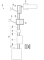
- FIG. 1 is a schematic explanatory diagram of a continuous casting device used when producing the copper alloy powder for metal AM according to the present embodiment.
- FIG. 2 is a flow diagram of a method for producing a layered object according to the present embodiment.
- FIG. 2 is a schematic explanatory diagram of another continuous casting device used in producing the copper alloy powder for metal AM according to the present embodiment.
- FIG. 1 is a diagram showing the results of Auger electron spectroscopy analysis of the outermost surface of a particle constituting the copper alloy powder for metal AM according to the present embodiment, and is a secondary electron image of the particle surface.
- FIG. 2 is a diagram showing the results of Auger electron spectroscopy analysis of the outermost surface of a particle constituting the copper alloy powder for metal AM according to the present embodiment, and is an element mapping image of the particle surface.
- 1 is an example of a graph showing the results of Auger electron spectroscopy analysis of the outermost surface of a particle constituting the copper alloy powder for metal AM according to the present embodiment, and shows an O intensity depth profile.
- 1 is an example of a graph showing the results of Auger electron spectroscopy analysis of the outermost surface of a particle constituting the copper alloy powder for metal AM according to this embodiment, and shows an intensity depth profile of Si.
- the copper alloy powder for metal AM according to the present embodiment is a copper alloy powder used for metal AM. Note that the copper alloy powder for metal AM according to the present embodiment is considered to be particularly suitable for the laser PBF method.
- the copper alloy powder for metal AM of this embodiment is an aggregate of particles made of a copper alloy containing Si, and a Si-concentrated layer is continuously formed on the surface of the copper alloy particles that make up the copper alloy powder for metal AM. That is, as shown in FIG. 1, the copper alloy particle 50 of the copper alloy powder for metal AM of this embodiment has a particle body (copper alloy particle) 51 made of a copper alloy containing Si, and a Si-concentrated layer 52 formed on the surface (or surface layer) of this particle body 51.
- the surface (particle surface) (or surface layer) of the copper alloy particle of the copper alloy powder for metal AM is a region from the outermost surface of the particle to a depth of 100 nm.
- the Si-enriched layer 52 is a layer in which a portion having a Si intensity amplification factor (defined below) of 2 or more is analyzed from the results of Auger electron spectroscopy on the surface of the particle body 51. This analysis method will be described below. Using a scanning Auger electron spectrometer PHI700xi manufactured by ULVAC-PHI, Inc., the signal intensity of Si element (IAES(t)) over measurement time (t) is measured every 30 seconds from the start of Auger electron signal measurement on the surface of the particle body 51 to be analyzed.
- a Si intensity amplification factor defined below
- the Si-enriched layer 52 is identified by Auger electron spectroscopy as follows.
- the signal intensity (I AES (t)) of the Si element is measured over the measurement time (t) every 30 seconds from the start of Auger electron signal measurement on the particle surface to be analyzed.
- Six or more regions where the I AES (t) for the Si element is roughly constant are then identified, and the average value of I AES (t) is calculated in these regions where the I AES (t) is constant. This average value is defined as the average background intensity (I AES , BG AVE ).
- the I AES (t) at all the acquired times t is divided by the I AES , BG AVE to obtain a numerical value.
- This numerical value is defined as I AES, NORM (t).
- I AES, NORM (t) is expressed by the following formula (1).
- I AES, NORM (t) I AES (t) / I AES , BG AVE Equation (1)
- I AES,NORM (t) increases continuously with decreasing measurement time in the Si-enriched layer 52.
- the start time of the region where this continuous increase in I AES,NORM (t) is observed is defined as the time t s0 which marks the end of the Si-enriched layer.
- ts0 is approximately 2 min.
- I AES,NORM (t) calculated by formula (1) is called the Si intensity amplification factor. According to Table 5, in an embodiment in which the Si-enriched layer 52 is present, a value of the Si intensity amplification factor exceeding 2 is clearly observed, and a situation in which the Si signal intensity is clearly stronger than the background intensity is confirmed.
- a Si-enriched layer 52 is present on the surface of the particle body 51.
- a portion of the Si-enriched layer 52 may have a Si intensity magnification factor of less than 2 to 1.7, for example.
- the Si-enriched layer 52 formed on the surface of the particle body 51 of the copper alloy particle 50 of the copper alloy powder for metal AM contains oxygen (O).
- the thickness of the Si-enriched layer 52 formed on the surface of the particle body 51 is preferably 1 nm or more and 100 nm or less.
- the thickness of the Si-enriched layer 52 is preferably 1 nm or more, and may be 5 nm or more, 10 nm or more, 20 nm or more, 30 nm or more, or 50 nm or more.
- the thickness of the Cr compound layer 52 is preferably 100 nm or less, and may be 95 nm or less, 90 nm or less, 80 nm or less, or 70 nm or less.
- the thickness of the Si-enriched layer 52 is determined by etching the surface of the copper alloy particles 50 of the copper alloy powder for metal AM by ion etching at an etching rate of 1.08 nm/min under the standard etching conditions, and analyzing the surface of the copper alloy particles 50 of the copper alloy powder for metal AM by Auger electron spectroscopy using a scanning Auger electron spectrometer PHI700xi manufactured by ULVAC-PHI, Inc. to obtain a Si mapping image showing the Si compound, and obtaining a silicon (Si) intensity depth profile (a graph showing the relationship between intensity and etching time shown in FIG. 7B).
- the copper alloy constituting the copper alloy particles 50 of the copper alloy powder for metal AM of this embodiment preferably contains Cr as an alloying element. This is because the addition of Cr to the copper alloy produces compounds of Cr and Si in the copper alloy, and in particular the compounds of Cr and Si present on the surface of the copper alloy particles contribute to improving the laser absorption rate.
- the copper alloy constituting the copper alloy particles 50 of the copper alloy powder for metal AM of this embodiment preferably contains Ni as an alloying element. This is because the addition of Ni to the copper alloy causes Ni to dissolve in the Cu crystal grains, which contributes to improving the laser absorptivity of the Cu crystal grains in the copper alloy particles.
- the content of Ni contained as an alloying element is preferably 3.0 mass% or less.
- the copper alloy constituting the copper alloy particles 50 of the copper alloy powder for metal AM of this embodiment preferably contains, as alloy elements, Cr in the range of 0.1 mass% to 0.8 mass%, Si in the range of 0.4 mass% to 0.8 mass%, Ni in the range of 1.8 mass% to 3.0 mass%, and the rest is composed of copper and impurities. That is, the copper alloy constituting the copper alloy particles 50 of the copper alloy powder for metal AM of this embodiment preferably has a composition equivalent to C18000.
- the alloy elements refer to Cr, Si, and Ni.
- the impurities referred to here are components including impurity elements described below as well as O, H, S, and N.
- the numerical accuracy error is ⁇ 10% (excluding O, H, S, and N).
- the lower limit of the Cr content is more preferably 0.2 mass% or more, and even more preferably 0.3 mass% or more.
- the upper limit of the Cr content is more preferably 0.8 mass% or less, and even more preferably 0.7 mass% or less.
- the lower limit of the Si content is more preferably 0.45 mass% or more, and even more preferably 0.5 mass% or more.
- the upper limit of the Si content is more preferably 0.7 mass% or less, and even more preferably 0.6 mass% or less.
- the lower limit of the Ni content is more preferably 1.9 mass% or more, and even more preferably 2.0 mass% or more.
- the upper limit of the Ni content is more preferably 2.9 mass% or less, and even more preferably 2.8 mass% or less.
- the copper alloy constituting the copper alloy particles 50 of the copper alloy powder for metal AM may contain additive elements and impurity elements (excluding O, H, S, and N) other than the alloy elements.
- the additive elements are elements that are intentionally added to the copper alloy particles 50 of the copper alloy powder for metal AM of this embodiment.
- the impurity elements (excluding O, H, S, and N) are elements that are unintentionally mixed into the copper alloy particles 50 of the copper alloy powder for metal AM of this embodiment, and originate from contamination during the manufacturing process or impurities contained in trace amounts in the raw materials.
- the impurity elements may be unavoidable impurities.
- additive elements and impurity elements (excluding O, H, S, and N) other than the alloy elements constituting the copper alloy particles 50 of the copper alloy powder for metal AM include Zr, Mg, Ti, Al, Zn, Ca, Sn, Pb, Fe, Mn, Te, Nb, P, Co, Sb, Bi, Ag, Ta, W, and Mo.
- the additive elements and impurity elements (excluding O, H, S, and N) other than the alloy elements may include at least one element selected from the group consisting of Zr, Mg, Ti, Al, Zn, Ca, Sn, Pb, Fe, Mn, Te, Nb, P, Co, Sb, Bi, and Ag, Ta, W, and Mo.
- the total amount of additive elements and impurity elements (excluding O, H, S, and N) other than the alloy elements constituting the copper alloy particles 50 of the copper alloy powder for metal AM may be 0.07 mass% or less, 0.06 mass% or less, or 0.05 mass% or less, preferably 0.04 mass% or less, more preferably 0.03 mass% or less, even more preferably 0.02 mass% or less, and even more preferably 0.01 mass% or less.
- the upper limit of the content of each of the additive elements and impurity elements (excluding O, H, S, and N) other than the alloy elements constituting the copper alloy particles 50 of the copper alloy powder for metal AM is preferably 30 ppm by mass or less, more preferably 20 ppm by mass or less, and even more preferably 15 ppm by mass or less.
- the 50% cumulative particle diameter D50 on a volume basis measured by a laser diffraction/scattering method is in the range of 5 ⁇ m or more and 120 ⁇ m or less
- the 10% cumulative particle diameter D10 is in the range of 1 ⁇ m or more and 80 ⁇ m or less
- the 90% cumulative particle diameter D90 is in the range of 10 ⁇ m or more and 150 ⁇ m or less.
- the lower limit of the 50% cumulative particle size D50 is more preferably 10 ⁇ m or more, and even more preferably 15 ⁇ m or more.
- the upper limit of the 50% cumulative particle size D50 is more preferably 100 ⁇ m or less, and even more preferably 90 ⁇ m or less.
- the lower limit of the 10% cumulative particle size D10 is more preferably 5 ⁇ m or more, and even more preferably 10 ⁇ m or more.
- the upper limit of the 10% cumulative particle size D10 is more preferably 70 ⁇ m or less, and even more preferably 60 ⁇ m or less.
- the lower limit of the 90% cumulative particle size D90 is more preferably 20 ⁇ m or more, and even more preferably 30 ⁇ m or more.
- the upper limit of the 90% cumulative particle size D90 is more preferably 140 ⁇ m or less, and even more preferably 120 ⁇ m or less.
- the manufacturing method of copper alloy powder for metal AM according to this embodiment includes a melting and casting step S01 for obtaining a copper alloy ingot, a copper alloy raw material preparation step S02 for processing the obtained copper alloy ingot into a wire rod to obtain a copper alloy raw material, and a powder processing step S03 for processing the copper alloy raw material into powder.
- a copper alloy ingot having a predetermined composition is produced.
- the melting and casting process S01 includes a melting step, an alloying element addition step, and a continuous casting step.
- a copper alloy ingot 1 is produced using a continuous casting apparatus 10 shown in FIG.
- This continuous casting apparatus 10 includes a melting furnace 11, a tundish 12 arranged downstream of the melting furnace 11, a connecting trough 13 connecting the melting furnace 11 and the tundish 12, an addition section 14 for adding alloy elements in the tundish 12, a continuous casting mold 15 arranged downstream of the tundish 12, and a pouring nozzle 16 for pouring molten copper alloy from the tundish 12 into the continuous casting mold 15.
- the copper raw material is melted in a non-oxidizing atmosphere (an inert gas atmosphere or a reducing atmosphere) to obtain molten copper 3 (melting step).
- the copper raw material melted in the melting furnace 11 is high-purity copper having a purity of 99.99 mass% or more (e.g., high-purity electrolytic copper or oxygen-free copper).
- the copper raw material to be melted is high-purity copper of 4N grade (99.99 mass%) or more, more preferably high-purity copper of 5N grade (99.999 mass%) or more, and even more preferably high-purity copper of 6N (99.9999 mass%) or more.
- the obtained molten copper 3 is preferably oxygen-free molten copper.
- the obtained molten copper 3 is supplied to the tundish 12 while maintaining a non-oxidizing atmosphere (an inert gas atmosphere or a reducing atmosphere).
- the connecting trough 13 is disposed between the melting furnace 11 and the tundish 12, and the molten copper 3 passes through the inside of the connecting trough 13 in a non-oxidizing atmosphere.
- the molten copper 3 is held in a non-oxidizing atmosphere (an inert gas atmosphere or a reducing atmosphere).
- the connecting trough 13, and the tundish 12 are in a non-oxidizing atmosphere (an inert gas atmosphere or a reducing atmosphere), the gas components (O, H) in the molten copper 3 are reduced.
- alloy elements Cr, Si, Ni, etc.
- additive elements may be appropriately added here.
- alloying elements By adding alloying elements to the molten copper 3 in which the gas components (O, H) have been sufficiently reduced, the yield of the alloying elements added is good, so that the amount of the alloying elements used can be reduced, and the manufacturing cost of the copper alloy can be reduced.
- alloying elements By adding alloying elements to the molten copper 3 flowing inside the tundish 12, the alloying elements can be uniformly dissolved, and a molten copper alloy having stable component values can be continuously produced.
- the obtained molten copper alloy is poured into a continuous casting mold 15 through a pouring nozzle 16 to continuously produce a copper alloy ingot 1 (continuous casting process).
- a copper alloy ingot having a circular cross section is produced.
- the obtained copper alloy ingot 1 has an O concentration of 10 ppm by mass or less and an H concentration of 5 ppm by mass or less.
- the S concentration is preferably 15 mass ppm or less.
- the total content of impurity elements other than Cu and alloy elements is preferably 0.04 mass% or less.
- the total concentration of O, H and S is preferably 20 mass ppm or less.
- the copper alloy raw material preparation step S02 includes an extrusion step, a drawing step, and a cutting step.
- a copper alloy ingot having a circular cross section is heated and processed by hot extrusion into a rod having a predetermined diameter (extrusion step).
- the heating temperature during the hot extrusion process is preferably set within a range of 700° C. or more and 1000° C. or less.
- the obtained rod is subjected to drawing to produce a wire of a specified diameter (drawing process).
- drawing process There are no particular restrictions on the temperature of the drawing process, but it is preferable to carry out the process at a temperature between -200°C and 200°C, which results in cold or warm rolling, and room temperature is particularly preferable.
- the resulting wire is then cut to a predetermined length to provide a copper alloy raw material (cutting step).
- the obtained copper alloy raw material has an O concentration of 10 mass ppm or less and an H concentration of 5 mass ppm or less.
- the S concentration in the obtained copper alloy raw material is preferably 15 mass ppm or less.
- the total content of impurity elements (excluding O, H, and S) other than Cu and alloy elements in the obtained copper alloy raw material is preferably 0.04 mass% or less.
- the copper alloy raw material obtained in the copper alloy raw material preparation step S02 is subjected to an atomization process to produce copper alloy powder for metal AM.
- This powder processing step S03 includes a melting step, an atomizing step, and a classification step.
- the melting step the copper alloy raw material is heated and melted to obtain a molten alloy.
- the melting atmosphere is preferably a non-oxidizing atmosphere.
- powder is obtained by, for example, gas atomization. That is, the molten alloy obtained in the melting process is sprayed with high-pressure gas to rapidly cool the droplets of the molten alloy, thereby producing powder having a spherical or similar shape.
- Inert gases such as argon and nitrogen can be used as the gas used in the gas atomization process.
- the obtained powder is classified to obtain a copper alloy powder having a predetermined particle size distribution.
- the melting temperature of the copper alloy raw material in the gas atomization process (the melting temperature during the gas atomization process) is preferably equal to or higher than the melting point of copper and equal to or lower than 1500° C.
- the melting temperature during the gas atomization process may be equal to or higher than 1085° C. and equal to or lower than 1500° C.
- the copper alloy powder for metal AM according to the present embodiment is manufactured by the above-mentioned steps.
- the O concentration is preferably 1000 mass ppm or less
- the H concentration is preferably 5 mass ppm or less
- the S concentration is preferably 10 mass ppm or less.
- the O concentration may be about 2700 ppm by mass or less, preferably 1000 ppm by mass or less, and more preferably 900 ppm by mass or less.
- the lower limit of the O concentration is not particularly limited, but may be a value that does not include 0 (or a value that exceeds 0).
- the H concentration may be 90 mass ppm or less, may be 60 mass ppm or less, and is preferably 5 mass ppm or less.
- the lower limit of the H concentration is not particularly limited, but may be a value that does not include 0 (or a value that exceeds 0).
- the S concentration may be 90 mass ppm or less, may be 60 mass ppm or less, and is preferably 30 mass ppm or less.
- the S concentration in the copper alloy powder for metal AM is more preferably 10 mass ppm or less.
- the lower limit of the S concentration is not particularly limited, but may be a value that does not include 0 (or a value that exceeds 0).
- atmospheric components contained in the atmosphere or during the process may cause the powder to contain atmospheric components.
- nitrogen derived from atmospheric components may be contained in the powder.
- the nitrogen concentration (N concentration) is preferably 30 mass ppm, more preferably 20 mass ppm, and even more preferably 10 mass ppm or less.
- the nitrogen concentration (N concentration) is more preferably 5 mass ppm or less.
- the lower limit of the N concentration is not particularly limited, but may be a value that does not include 0 (or a value that exceeds 0).
- the copper alloy powder for metal AM may contain additive elements and impurity elements other than the alloy elements to the extent that they do not affect the characteristics.
- the total amount of additive elements other than alloy elements and impurity elements may be 0.07 mass% or less, may be 0.06 mass% or less, may be 0.05 mass% or less, is preferably 0.04 mass% or less, is more preferably 0.03 mass% or less, is further preferably 0.02 mass% or less, and is further preferably 0.01 mass% or less.
- the upper limit of the content of each of additive elements other than alloy elements and impurity elements is preferably 30 mass ppm or less, more preferably 20 mass ppm or less, and even more preferably 15 mass ppm or less.
- the manufacturing method of an additively molded object in this embodiment includes a preparation process S101 for preparing the above-mentioned copper alloy powder for metal AM, a first process S121 for forming a powder layer containing the copper alloy powder for metal AM, and a second process S122 for solidifying the copper alloy powder for metal AM at a predetermined position in the powder layer to form a molding layer, and a modeling process S102 for producing an additively molded object by sequentially repeating these steps.
- a layered object having a predetermined shape is manufactured. Since the layered object uses the copper alloy powder for metal AM according to the present embodiment, the layered object has few structural defects such as voids and has excellent mechanical properties.
- the copper alloy powder for metal AM of this embodiment configured as described above is composed of copper alloy particles 50 containing Si, and Si is segregated on the surface of the copper alloy particles 50 that constitute the copper alloy powder for metal AM, and a Si-enriched layer 52 is formed on the outer surface of the particle body 51.
- the Si-enriched layer 52 formed on the surface of the particle body 51 is an oxide layer containing Si and O, it is possible to suppress the deterioration of the copper alloy powder for metal AM, and it is possible to more stably manufacture an even higher quality additively manufactured object with high reproducibility of the microstructure of the object produced by additive manufacturing and with fewer structural defects such as voids.
- the copper alloy powder for metal AM of this embodiment when the copper alloy constituting the copper alloy particles 50 contains Cr in the range of 0.1 mass% to 0.8 mass%, Si in the range of 0.4 mass% to 0.8 mass%, Ni in the range of 1.8 mass% to 3.0 mass%, and the rest is copper and impurities, by subjecting an additive manufacturing product made using this copper alloy powder for metal AM to an appropriate heat treatment, compounds can be precipitated, making it possible to manufacture an additive manufacturing product with excellent electrical conductivity, thermal conductivity, and strength.
- the 50% cumulative particle diameter D50 on a volume basis measured by the laser diffraction/scattering method is within the range of 5 ⁇ m or more and 120 ⁇ m or less, it has a particle size distribution suitable for metal AM, and it becomes possible to stably manufacture additive manufacturing objects.
- the volume-based 10% cumulative particle diameter D10 measured by the laser diffraction/scattering method is within the range of 1 ⁇ m or more and 80 ⁇ m or less, it has a particle size distribution suitable for metal AM, and it becomes possible to stably manufacture additive manufacturing objects.
- the volume-based 90% cumulative particle diameter D90 measured by the laser diffraction/scattering method is within the range of 10 ⁇ m or more and 150 ⁇ m or less, it has a particle size distribution suitable for metal AM, and it becomes possible to stably manufacture additive manufacturing objects.
- the manufacturing method for additive manufacturing of this embodiment uses the copper alloy powder for metal AM of this embodiment, which makes it possible to reproducibly produce the microstructure of the object produced by additive manufacturing, and to stably manufacture high-quality additive manufacturing objects with few structural defects such as voids.
- the copper alloy powder for metal AM and the method for manufacturing an additive manufacturing object according to the embodiment of the present invention have been described above.
- the present invention is not limited thereto and can be modified as appropriate without departing from the technical concept of the invention.
- the copper alloy powder for metal AM is produced by gas atomization, but this is not limited thereto, and the copper alloy powder for metal AM may be produced by water atomization, centrifugal atomization, plasma atomization, or the like.
- the copper alloy powder for metal AM obtained as described above may be appropriately heat-treated in a controlled atmosphere to stabilize the structure. Furthermore, in this embodiment, the copper alloy powder for metal AM suitable for the laser PBF method has been described as being produced, but this is not limited to this, and the copper alloy powder for metal AM applicable to other additive manufacturing methods may also be used.
- a heat treatment process may be performed in which heat treatment is performed at a temperature of 300° C. or more and the melting point of pure copper or less.
- a first heat treatment process may be performed in which heat treatment is performed at a temperature range of 800° C. or more and the melting point of pure copper or less, and after this first heat treatment process, a second heat treatment process may be performed in which heat treatment is performed at a temperature range of 300° C. or more and 800° C. or less.
- the continuous casting apparatus shown in FIG. 3 is used to produce a copper alloy ingot, but the present invention is not limited to this, and other casting apparatuses may be used.
- a continuous casting device 101 shown in FIG. 5 may be used.
- This continuous casting device 101 includes an oxygen-free copper supply means (molten copper supply section) 102 arranged at the most upstream portion, a heating furnace 103 arranged downstream thereof, a tundish 104 arranged downstream of the heating furnace 103 and supplied with molten copper, molten metal supply passages 105a, 105b, and 105c connecting the oxygen-free supply means 102 to the heating furnace 103, a trough 106 connecting the heating furnace 103 and the tundish 104, addition means (addition sections) 107 and 108 for adding alloy elements in a non-oxidizing atmosphere, and a continuous casting mold 142.
- the oxygen-free copper supply means 102, the heating furnace 103, the tundish 104, the molten metal supply passages 105a, 105b, and 105c, and the trough 106 each have a non-oxidizing atmosphere inside.
- the oxygen-free copper supply means 102 is composed of a melting furnace 121 for melting the copper raw material, a holding furnace 122 for temporarily holding the molten copper obtained by melting in the melting furnace 121, a degassing treatment device 124 for removing oxygen and hydrogen from the molten copper, and molten metal supply paths 105a, 105b, and 105c that connect these.
- the degassing treatment device 124 has a gas bubbling device as stirring means for stirring the molten copper therein, and removes oxygen and hydrogen from the molten copper by bubbling with an inert gas, for example.
- the molten metal supply passages 105a, 105b, and 105c have a non-oxidizing atmosphere therein to prevent the molten copper and the oxygen-free copper molten metal from being oxidized.
- the non-oxidizing atmosphere is formed by blowing a mixed gas of nitrogen and carbon monoxide or an inert gas such as argon into the molten metal supply passages.
- a first adding means 107 disposed in the heating furnace 103 and a second adding means 108 disposed in the tundish 104 are provided.
- the alloying elements are added to the oxygen-free copper molten metal stored in the heating furnace 103.
- the oxygen-free copper molten metal stored in the storage section is heated by a high-frequency induction coil, and the melting of the added alloying elements is promoted.
- the alloying elements are continuously or intermittently charged from the second adding means 108 provided in the tundish 104, the alloying elements are added to the molten oxygen-free copper flowing in the tundish 104.
- the molten oxygen-free copper flowing in the tundish 104 is heated in the heating furnace 103 and has a high temperature, and also flows within the tundish 104, the dissolution of the added alloying elements is promoted.
- Example of the invention First, by the manufacturing method described in the embodiment, a copper raw material made of 4N grade high purity copper was used to produce an ingot of C18000 having the composition shown in Table 1. Next, the produced C18000 ingot was used as a raw material to produce copper alloy powder for metal AM having the composition shown in Table 2 by gas atomization using argon gas, and the powder was classified to a particle size suitable for the powder bed of metal AM. The melting temperature during the gas atomization process was 1400°C.
- the particle size distribution of the copper alloy powder for metal AM of the present invention was measured using MT3300EXII manufactured by Microtrac Co., Ltd., and the particle size distribution was as follows: 10% cumulative particle size on a volume basis was 15 ⁇ m, 50% cumulative particle size was 24 ⁇ m, and 90% cumulative particle size was 38 ⁇ m.
- a Si-enriched layer was observed on the surface of the copper alloy particles, as described later.
- a small piece of an additive manufacturing object was produced using a commercially available laser PBF device at an energy density of 13 J/ mm2 .
- Comparative Example As a comparative example, a copper alloy powder for metal AM having the composition of C18000, which does not have a Si-enriched layer formed on the particle surface, unlike the examples of the present invention, was prepared.
- particle size distribution measurement was performed using MT3300EXII manufactured by Microtrac, and the particle size distribution was as follows: 10% cumulative particle size on a volume basis was 16 ⁇ m, 50% cumulative particle size was 28 ⁇ m, and 90% cumulative particle size was 45 ⁇ m.
- a scanning Auger electron spectrometer PHI700xi manufactured by ULVAC-PHI, Inc. was used to measure the signal intensity ( IAES (t)) of the Si element over the measurement time (t) for the particle body to be analyzed every 30 seconds from the start of measurement of the Auger electron signal on the surface. Then, for one of these I AES (t), six or more regions where the I AES (t) for the Si element was roughly constant were identified, and the average value of I AES (t) was calculated in these regions where the I AES (t) was constant.
- I AES, BG AVE average background intensity
- I AES, NORM (t) I AES (t) / I AES , BG AVE Equation (1)
- I AES,NORM (t) increased continuously with decreasing measurement time in the Si-enriched layer.
- the start time of the region where this continuous increase in I AES,NORM (t) was observed was defined as t s0 , which is the end of the Si-enriched layer.
- t s0 was about 2 min
- I AES, NORM (t) was taken as the Si intensity amplification factor.
- the measurement time (t), signal intensity of Si element (I AES (t)), and Si intensity magnification factor I AES, NORM (t) of the copper alloy powder for metal AM of the present invention obtained by the above measurements and calculations are shown in Table 5.
- the average background intensity (I AES , BG AVE ) of the present invention example was 2847.57.
- Table 5 in the present invention examples in which a Si-enriched layer exists, a Si intensity magnification factor exceeding 2 was clearly observed, and it was confirmed that the Si signal intensity was clearly stronger than the background intensity. Therefore, it was confirmed that a Si-enriched layer exists in the particle body of the copper alloy powder for metal AM of the present invention example.
- no Si strength magnification factor exceeding 2 was observed, and it was considered that no Si-enriched layer was present in the particle body of the copper alloy powder for metal AM.
- composition of ingot and copper alloy powder for metal AM The O concentration in the ingots shown in Table 1, the copper alloy powders for metal AM of the present invention, and the copper alloy powders for metal AM of the comparative examples was determined by inert gas fusion-infrared absorption method, the H concentration by inert gas fusion-thermal conductivity method, and the S concentration by combustion-infrared absorption method.
- concentrations of components other than these substances, except for copper were determined by a combination of X-ray fluorescence analysis, glow discharge mass spectrometry, and inductively coupled plasma mass spectrometry. The evaluation results are shown in Tables 1 and 2.
- the density of the layered object was evaluated from the cross section of the layered object and the area occupied by voids observed in the cross section of the layered object. In this specification, this density is defined as the density of the object.
- the density of the molded object was evaluated by first defining the cross-sectional area of the object to be measured (this is called the evaluation cross-sectional area; 3.4 mm square), and then checking for voids within this measurement cross-sectional area, and calculating the area occupied by voids in the evaluation cross-sectional area. The density of the molded object was then defined as (evaluation cross-sectional area - void-occupied area)/evaluation cross-sectional area. The evaluation results of the density of the molded object are shown in Table 3.
- Figures 6A and 6B show the results of Auger electron spectroscopy analysis of the particle surface of the copper alloy powder for metal AM of the present invention. As shown in Figures 6A and 6B, it was confirmed that a Si-enriched layer exists on the surface (or surface layer) of the copper alloy particles of the copper alloy powder for metal AM of the present invention, and that the particle surface is entirely covered with the Si-enriched layer.
- FIG. 7A and 7B show the intensity depth profiles of Si and O obtained by Auger electron spectroscopy of the particle surface of the copper alloy powder for metal AM of the present invention.
- the etching rate of each element alone or compounds generated by each element on the particle surface of the copper alloy powder of the present invention example in the experimental system of this Auger electron spectroscopy is not clear, but since the etching rate of SiO2 in the experimental system of this Auger electron spectroscopy is 1.08 nm/min, it is considered that the structure after ion etching for 7 minutes is approximately 10 nm thick.
- the Si concentration is high on the surface side of the powder, and it was confirmed that a Si-enriched layer was formed on the surface of the powder. From this result, it is considered that the thickness of the Si-enriched layer is generally in the range of about 1 nm to 100 nm.
- Si does not segregate on the surface of the powder, and it is recognized that a Si-enriched layer is not formed on the surface of the powder.
- the O concentration on the surface side of the copper alloy powder for metal AM of the present invention is high, and the Si-enriched layer formed on the surface of the powder contains oxygen (O). That is, it is considered that the Si-enriched layer in the copper alloy powder for metal AM of the present invention is composed of a layer containing Si and O. Thus, it is considered that oxygen is also detected at the same time in the Si-enriched layer in the copper alloy powder for metal AM of the present invention, and surface deterioration of the copper alloy powder can be relatively suppressed.
- the copper alloy powder for metal AM of the present invention contains oxygen as a copper alloy, so that a certain amount of oxygen exists in the particle body, which is considered to constitute the background concentration of oxygen in the particle body.
- a gradient of oxygen concentration can be generated on the particle surface, mainly due to the powdering process, on the order of the thickness of the above-mentioned Si-enriched layer.
Abstract
This metal AM copper alloy powder for use in metal additive manufacturing (AM) comprises a copper alloy containing Si. An Si-enriched layer is continuously formed on the surface of copper alloy particles of which the powder is composed.
Description
本発明は、金属アディティブ・マニュファクチャリング(金属AM)技術に最適な金属AM用銅合金粉末、および、積層造形物の製造方法に関する。
本願は、2022年10月24日に、日本に出願された特願2022-169921号に基づき優先権を主張し、その内容をここに援用する。 The present invention relates to a copper alloy powder for metal additive manufacturing (metal AM) that is optimal for metal AM technology, and a method for manufacturing an additively manufactured object.
This application claims priority based on Japanese Patent Application No. 2022-169921, filed on October 24, 2022, the contents of which are incorporated herein by reference.
近年、様々な立体形状を有する金属部品を製造する手法として、主に原料として粉を用いて金属3Dプリンターで製品を造形する金属AM技術が実用化されている。金属粉末を用いた主な金属AM技術としては、電子ビームやレーザー光を用いた粉末床溶融法(パウダー・ベッド・フュージョン:PBF)、バインダジェット法等が挙げられる。
ここで、銅合金は、導電性、熱伝導性、機械的特性、耐摩耗性、耐熱性など工業的な応用に適した多数の基本的性質を有しており、各種部材の素材として利用されている。そこで、近年、宇宙、電気部品応用など様々な分野において、銅合金粉末を用いた金属AMにより、様々な形状の部材を形成することが試行され、金属AMで製造された銅及び銅合金の部品のニーズが高まっている。 In recent years, metal AM technology, which uses powder as the main raw material and creates products using a metal 3D printer, has been put to practical use as a method for manufacturing metal parts with various three-dimensional shapes. Major metal AM technologies using metal powder include powder bed fusion (PBF) using electron beams or laser light, and binder jetting.
Copper alloys have many basic properties suitable for industrial applications, such as electrical conductivity, thermal conductivity, mechanical properties, wear resistance, and heat resistance, and are used as materials for various components. In recent years, attempts have been made to form components of various shapes by metal AM using copper alloy powder in various fields such as space and electrical component applications, and there is an increasing need for copper and copper alloy components manufactured by metal AM.
例えば、特許文献1には、CrとSiのいずれかを有する銅合金粉末を用いて、金属AMによる積層造形物を作成する技術が提案されている。
また、特許文献2には、CrとZrを有する銅合金粉末を用いて、金属AMによる積層造形物を作成する技術が提案されている。 For example,Patent Document 1 proposes a technique for producing an additive manufacturing object by metal AM using a copper alloy powder containing either Cr or Si.
Moreover,Patent Document 2 proposes a technique for producing an additive manufacturing object by metal AM using a copper alloy powder containing Cr and Zr.
また、特許文献2には、CrとZrを有する銅合金粉末を用いて、金属AMによる積層造形物を作成する技術が提案されている。 For example,
Moreover,
金属AMにより造形される金属構造体は、様々な用途に応じて何らかの構造部材として用いられることになるため、積層造形体の中にボイドが存在する場合や金属材料としての微細構造が不均一である場合には、熱機械的また電気的な信頼性の点で問題となる。
現在、金属AMで最も多く使用されている造形方式はレーザーPBFであり、銅及び銅合金においても、レーザーPBFによる造形が試みられてきている。
ところで、レーザー光や電子線を照射する方法で積層造形する際には、まず薄い粉末の層を形成し(粉末床)、続いてこの粉末床にレーザーや電子線を局所的に照射して材料を溶融凝固させる。しかし、銅及び銅合金においては、鉄、チタン、ニッケル系などの他の金属材料と比較して、銅そのものが可視、赤外域の光に対する反射率が高いことなどが原因となり、レーザーPBFの過程で銅合金粉末の溶融挙動が不安定となり、作製された積層造形物の内部にボイドが発生しやすく、レーザーPBFで製造した造形体の品質が安定しない、生産性が悪いなどの課題が山積しており、レーザーPBFにより製造された銅及び銅合金の生産性及び品質の改善が求められてきている。 Metal structures created by metal AM will be used as structural components for a variety of applications; therefore, if voids are present in the additively created body or if the microstructure of the metal material is uneven, this can cause problems in terms of thermomechanical and electrical reliability.
Currently, the most commonly used manufacturing method for metal AM is laser PBF, and attempts are being made to use laser PBF for manufacturing copper and copper alloys as well.
Incidentally, when performing additive manufacturing using a method of irradiating a laser beam or an electron beam, a thin layer of powder is first formed (powder bed), and then the powder bed is locally irradiated with a laser or an electron beam to melt and solidify the material. However, in the case of copper and copper alloys, compared with other metal materials such as iron, titanium, and nickel, copper itself has a high reflectance in the visible and infrared ranges, which causes the melting behavior of the copper alloy powder to become unstable during the laser PBF process, and voids are likely to occur inside the manufactured additive manufacturing product, resulting in a number of problems such as unstable quality of the product manufactured by laser PBF and poor productivity, and there is a demand for improvements in the productivity and quality of copper and copper alloys manufactured by laser PBF.
現在、最も広く使用されている金属AM用原料の形態は粉末である。例えば、レーザーPBFを用いた金属AMにおいては、原料粉末を構成する各粒子の表面層の電磁波とのカップリング・相互作用による粒子の電磁波の吸収特性が、原料粉末の溶融挙動に影響を及ぼし、部品の生産性や部品の欠陥密度を含む品質に大きく影響する。例えば、粉末床を用いる金属AMプロセスにおいては、一回の積層過程で形成される粉末床の厚みは例えば数10μm程度であり(非特許文献1)、収束した電磁波をこのような比較的薄い粉末床に照射することにより原料粉末を溶融させ、更に数多くの積層と溶融凝固を繰り返すことにより所望の造形構造を実現する。粉末床を用いるこのような積層造形の素過程に大きな影響を及ぼすのが固体の電磁波の吸収特性であり、例えば、固体の電磁波の吸収特性は材料組成により影響されるため、粉末の材料組成や微細構造の均一性を高めることは、積層造形物全体において安定した品質を実現することや高い生産性の実現において極めて重要となる。
Currently, the most widely used form of raw material for metal AM is powder. For example, in metal AM using laser PBF, the electromagnetic wave absorption characteristics of the particles due to coupling and interaction with the electromagnetic waves of the surface layer of each particle constituting the raw material powder affect the melting behavior of the raw material powder, and greatly affect the productivity of parts and the quality including the defect density of the parts. For example, in a metal AM process using a powder bed, the thickness of the powder bed formed in one stacking process is, for example, about several tens of μm (Non-Patent Document 1), and the raw material powder is melted by irradiating such a relatively thin powder bed with converged electromagnetic waves, and the desired modeling structure is realized by repeating numerous stacking and melting and solidification. The electromagnetic wave absorption characteristics of solids have a significant impact on the elementary process of such additive manufacturing using a powder bed. For example, since the electromagnetic wave absorption characteristics of solids are affected by the material composition, improving the uniformity of the powder material composition and microstructure is extremely important for achieving stable quality and high productivity in the entire additive manufacturing product.
ここで、銅及び銅合金における電磁波の吸収特性は、例えば、単純に銅以外の成分として、目的のレーザー波長の吸収率が高い物質を添加することで改善可能である。しかしながら、過去の多くの冶金研究が示すように、銅及び銅合金をある応用に供する場合、その応用に必要な特性は、銅に添加される元素の種類とその添加量が適切に選択されることにより初めて実現される。従って、銅や銅合金の金属AM造形体の生産性や品質改善のために、言い換えると、銅や銅合金の原料粉末のレーザー吸収の改善のために、最適化された組成の銅や銅合金にレーザー吸収率の高い各種異元素を添加したり、その添加量を増加させたりするなどの単純なアプローチは、各種応用に必要な銅合金の性能を悪化させる可能性がある。従って、各種応用に必要な銅合金の性能を十分に確保することが可能な材料組成を維持しながら、レーザー吸収特性が改善された金属AM用銅合金粉末を実現することが求められてきた。
Here, the electromagnetic wave absorption characteristics of copper and copper alloys can be improved, for example, by simply adding a substance with a high absorption rate of the target laser wavelength as a component other than copper. However, as many past metallurgical studies have shown, when copper and copper alloys are used for a certain application, the characteristics required for that application can only be realized by appropriately selecting the type and amount of elements added to copper. Therefore, in order to improve the productivity and quality of metal AM objects made of copper or copper alloys, in other words, to improve the laser absorption of raw powders of copper or copper alloys, a simple approach such as adding various foreign elements with high laser absorption rates to copper or copper alloys of optimized composition or increasing the amount of such elements added may deteriorate the performance of copper alloys required for various applications. Therefore, there has been a demand for realizing copper alloy powders for metal AM with improved laser absorption characteristics while maintaining a material composition that can fully ensure the performance of copper alloys required for various applications.
粉末のレーザー吸収特性の改善のための一つの重要なアプローチは、粉末を構成する各粒子表面の表面改質により各粒子のレーザー吸収能を改善することである。この表面改質のためには、所望の銅合金組成を有する粉末の各粒子の表面に、金属AMで使用するレーザー波長に対し高い吸収率を示す物質のコーティングを施すことが考えられる。このような粒子表面のコーティングのアプローチとして、所望のコーティング材料を湿式や気相プロセスを用いて粒子表面に形成することがあり得る。しかしながら、このようなコーティングプロセスでは、各粒子でのコーティング層の厚みの制御だけではなく、粉末全体でのコーティング厚みやコーティング材料の均質性の再現性の問題が付きまとい、結果として造形体の生産性や品質において数々の課題が発生することになる。
One important approach to improving the laser absorption properties of powder is to improve the laser absorption ability of each particle by surface modification of each particle that constitutes the powder. For this surface modification, it is possible to apply a coating of a substance that exhibits high absorption rate for the laser wavelength used in metal AM to the surface of each particle of the powder having the desired copper alloy composition. As an approach to coating the particle surface, a desired coating material may be formed on the particle surface using a wet or gas phase process. However, such a coating process is plagued with problems not only in controlling the thickness of the coating layer on each particle, but also in reproducibility of the coating thickness and homogeneity of the coating material throughout the powder, resulting in a number of issues in the productivity and quality of the molded object.
また、銅合金においては、過去の様々な研究開発の結果、高い導電性を維持しながら高い機械強度を実現した材料や、耐熱性に優れる材料などが既に開発されており、金属AMにおいても、既存のこのような高性能銅合金材料を用いて所望の形状を有する金属AM部品を実現したい社会的要請がある。
しかし、コーティングにより形成した特定成分の量を制御しながら、最終造形物の銅合金の材料組成を制御することは、大きな製造工程の負荷となるだけでなく、組成ばらつきや微細構造のばらつきに起因する造形部品の性能の悪化、部品の量産性の悪化、また部品の品質の維持の面など、多数の大きな問題を抱える懸念があった。 Furthermore, as a result of various past research and development efforts, copper alloy materials that achieve high mechanical strength while maintaining high electrical conductivity and materials with excellent heat resistance have already been developed, and in the field of metal AM, there is a social demand to realize metal AM parts having desired shapes using such existing high-performance copper alloy materials.
However, controlling the amount of specific components formed by the coating while also controlling the material composition of the copper alloy in the final product not only places a significant burden on the manufacturing process, but there were concerns that it could result in a number of major problems, such as deterioration of the performance of the molded parts due to variations in composition and microstructure, deterioration of mass producibility of parts, and issues with maintaining the quality of the parts.
また、金属AM造形体の構造欠陥の原因となる一つの因子として、ガスなどの巻き込みに起因するボイドの発生がある。従来の銅合金粉末を用いてPBF法で積層造形した場合、粉末溶融時に、銅合金粉末に内包される不純物が原因となりガスが発生し、溶融した銅合金や凝固した銅合金がガス成分をトラップし、作製された積層造形物の内部にボイドが生じることがあり、安定して高品質な積層造形物を作製することができないおそれがあった。
Furthermore, one of the factors that can cause structural defects in metal AM objects is the generation of voids due to the entrapment of gases, etc. When conventional copper alloy powder is used for additive manufacturing using the PBF method, gas is generated due to impurities contained in the copper alloy powder when the powder is melted, and the molten copper alloy or solidified copper alloy can trap the gas components, resulting in the generation of voids inside the additive object produced, which can make it difficult to consistently produce high-quality additive objects.
また、原料の粉末床にレーザー光や電子線を照射して積層造形する場合、レーザー光などが照射される各場所の粉末粒子の組成再現性を含む原料粉末に関わる微細構造の再現性が欠如している場合、粉末の溶融挙動が不均一となり、その結果、造形体内部にボイドなどの構造欠陥の発生を誘発したり、造形体の金属組成の不均一性による機械特性の悪化を生じさせたりするおそれがあった。
In addition, when additive manufacturing is performed by irradiating a powder bed of the raw material with laser light or electron beams, if there is a lack of reproducibility of the microstructure of the raw material powder, including the reproducibility of the powder particle composition at each location irradiated with the laser light, the melting behavior of the powder becomes non-uniform, which can result in the occurrence of structural defects such as voids inside the molded object, or the deterioration of mechanical properties due to non-uniformity in the metal composition of the molded object.
また、このような原料粉末の微細構造の再現性は、粉末の材料組成の再現性を含み、バインダジェット法など他の金属AMの工法においても同様な問題となっていた。銅合金の金属AMにおいては、このような各種の原料の課題のため生産性の改善が大きな課題であった。
Furthermore, the reproducibility of the microstructure of such raw material powders, including the reproducibility of the powder's material composition, is a similar problem with other metal AM methods such as the binder jet method. In metal AM of copper alloys, improving productivity is a major challenge due to issues with the various raw materials.
この発明は、前述した事情に鑑みてなされたものであって、金属AMにより作製した造形体の微細構造の再現性が高く、ボイド等の構造欠陥が少ない高品質な積層造形物を安定して製造可能な金属AM用銅合金粉末、および、積層造形物の製造方法を提供することを目的とする。
This invention was made in consideration of the above-mentioned circumstances, and aims to provide a copper alloy powder for metal AM that can stably produce high-quality additively molded objects with high reproducibility of the microstructure of objects produced by metal AM and few structural defects such as voids, and a method for producing additively molded objects.
この課題を解決するために、実応用に必要な銅合金組成を有しながらも、金属AMプロセスを用いて高性能で高品質な銅合金部品を高い生産性で実現するための銅合金粉末を製造するための研究開発を行った。その結果、高純度の銅合金を原料として用いて粉末化処理を行った場合、銅合金粉末全体としては不純物が少なくかつ均一な組成を維持しながら、銅合金粉末中の個別の粒子表面に着目すると、レーザーが照射されることになる銅合金粒子表面に薄層が形成されていることが見いだされた。更に、この銅合金粒子表面に形成された薄層においては、バルクの銅合金粒子内部と比較し、銅よりも高いレーザー吸収を示す粉末構成元素が高頻度で存在するという特徴ある構造が、粉末への個別のコーティングプロセスや付加的なプロセスを経ることなく、銅合金原料からの直接的な粉末化プロセスにおいて自発的に生成することが見出された。
In order to solve this problem, we conducted research and development to manufacture copper alloy powder that has the copper alloy composition required for practical applications, but can also be used to produce high-performance, high-quality copper alloy parts with high productivity using a metal AM process. As a result, when a high-purity copper alloy is used as a raw material and powder processing is performed, it was found that while the copper alloy powder as a whole has few impurities and maintains a uniform composition, when focusing on the surfaces of individual particles in the copper alloy powder, a thin layer is formed on the copper alloy particle surface that is irradiated with a laser. Furthermore, it was found that in the thin layer formed on the copper alloy particle surface, compared to the interior of the bulk copper alloy particle, a characteristic structure in which powder constituent elements that exhibit higher laser absorption than copper are frequently present is spontaneously generated in the direct powder processing process from the copper alloy raw material, without going through an individual coating process or additional process on the powder.
このような銅合金粒子表面の構造的特徴に加えて、高純度の銅合金原料に由来した銅合金粉末であることにより、ガス成分につながる不純物が少ないことで溶融時のガス発生を抑制することにより、高い熱的、電気的、機械的特性を有しながら、緻密な銅合金造形体を実現し、更にこのような高い性能を示す銅合金造形体の高い生産性と高い品質を実現することが可能な金属AM用銅合金粉末が製造できることを見出した。
In addition to these structural features of the copper alloy particle surface, the copper alloy powder is derived from high-purity copper alloy raw materials, which means that there are fewer impurities that lead to gas components, suppressing the generation of gas during melting. This allows for the realization of dense copper alloy molded bodies with high thermal, electrical, and mechanical properties, and furthermore, it has been discovered that it is possible to manufacture copper alloy powder for metal AM that can achieve high productivity and high quality of copper alloy molded bodies that exhibit such high performance.
不純物が少ない銅原料に由来し、Siが添加された銅合金をアトマイズ処理することにより作製した銅合金粉末において、銅合金の溶湯を噴霧するアトマイズ工程における急速な微細化と温度変化に誘起される微細構造変化により、銅合金粉末を構成する粒子表面にSi濃化層を自己形成的かつ連続的に形成させることに成功した。
このような特徴的な表面構造を有する粒子から成る金属AM用銅合金粉末を用いて銅合金を積層造形した場合には、積層造形物中のボイドの発生を大幅に削減可能であり、緻密な銅合金の積層造形物を作製することが可能であるとの知見を得た。このような造形性に優れる銅合金粉末は従来の銅合金粉末よりも高い生産性を実現すると考えられる。 In copper alloy powder produced by atomizing copper alloys derived from copper raw materials with few impurities and containing added Si, the rapid micronization during the atomization process in which molten copper alloy is sprayed and the microstructural changes induced by temperature changes have succeeded in self-forming and continuous formation of a Si-enriched layer on the particle surfaces that make up the copper alloy powder.
It has been found that when copper alloy powder for metal AM made of particles having such a characteristic surface structure is used for additive manufacturing of copper alloy, it is possible to significantly reduce the occurrence of voids in the additive manufactured product, and it is possible to produce a dense additive manufactured product of copper alloy. It is believed that such copper alloy powder with excellent formability will achieve higher productivity than conventional copper alloy powders.
本発明は、上述の知見に基づいてなされたものであって、本発明の態様1の金属AM用銅合金粉末は、金属AMに用いられる金属AM用銅合金粉末であって、Siを含有する銅合金からなり、粉末を構成する銅合金粒子の表面にSi濃化層が連続的に形成されていることを特徴としている。
The present invention was made based on the above findings, and the copper alloy powder for metal AM of aspect 1 of the present invention is a copper alloy powder for metal AM used in metal AM, which is made of a copper alloy containing Si, and is characterized in that a Si-enriched layer is continuously formed on the surface of the copper alloy particles that make up the powder.
本発明の態様1の金属AM用銅合金粉末によれば、Siを含有する銅合金からなり、粉末を構成する銅合金粒子の表面にSi濃化層が連続的に形成されていることにより、金属AMにより作製した造形体の微細構造の再現性が高く、ボイド等の構造欠陥が少ない高品質な積層造形物を安定して製造することが可能となる。
The copper alloy powder for metal AM according to aspect 1 of the present invention is made of a copper alloy containing Si, and a Si-enriched layer is continuously formed on the surface of the copper alloy particles that make up the powder. This makes it possible to stably manufacture high-quality additive manufacturing objects with high reproducibility of the microstructure of the objects produced by metal AM and with few structural defects such as voids.
本発明の態様2は、態様1の金属AM用銅合金粉末において、前記銅合金はCrを含有していることが好ましい。
本発明の態様2の金属AM用銅合金粉末によれば、CrとSiを含有する銅合金からなり、銅合金粒子の表面にSi濃化層が連続的に形成されていることにより、金属AMにより作製した造形体の微細構造の再現性が高く、ボイド等の構造欠陥が少ない高品質な積層造形物を安定して製造することが可能となる。 In a second aspect of the present invention, in the copper alloy powder for metal AM according to the first aspect, the copper alloy preferably contains Cr.
According to the copper alloy powder for metal AM ofaspect 2 of the present invention, which is made of a copper alloy containing Cr and Si, and has a Si-enriched layer continuously formed on the surface of the copper alloy particles, it is possible to stably produce high-quality additively molded objects with high reproducibility of the microstructure of the objects produced by metal AM and with few structural defects such as voids.
本発明の態様2の金属AM用銅合金粉末によれば、CrとSiを含有する銅合金からなり、銅合金粒子の表面にSi濃化層が連続的に形成されていることにより、金属AMにより作製した造形体の微細構造の再現性が高く、ボイド等の構造欠陥が少ない高品質な積層造形物を安定して製造することが可能となる。 In a second aspect of the present invention, in the copper alloy powder for metal AM according to the first aspect, the copper alloy preferably contains Cr.
According to the copper alloy powder for metal AM of
本発明の態様3は、態様1または態様2の金属AM用銅合金粉末において、前記Si濃化層が酸素を含有していることが好ましい。
本発明の態様3の金属AM用銅合金粉末によれば、銅合金粒子の表面に形成された前記Si濃化層が酸素を含有していることから、金属AM用銅合金粉末の変質を抑制でき、金属AMにより作製した造形体の微細構造の再現性が高く、ボイド等の構造欠陥が少ない高品質な積層造形物をさらに安定して製造することが可能となる。 In a third aspect of the present invention, in the copper alloy powder for metal AM according to the first or second aspect, the Si-enriched layer preferably contains oxygen.
According to the copper alloy powder for metal AM ofaspect 3 of the present invention, since the Si-enriched layer formed on the surface of the copper alloy particles contains oxygen, deterioration of the copper alloy powder for metal AM can be suppressed, and the microstructure of the shaped body produced by metal AM can be highly reproducible, making it possible to more stably produce high-quality additively shaped objects with fewer structural defects such as voids.
本発明の態様3の金属AM用銅合金粉末によれば、銅合金粒子の表面に形成された前記Si濃化層が酸素を含有していることから、金属AM用銅合金粉末の変質を抑制でき、金属AMにより作製した造形体の微細構造の再現性が高く、ボイド等の構造欠陥が少ない高品質な積層造形物をさらに安定して製造することが可能となる。 In a third aspect of the present invention, in the copper alloy powder for metal AM according to the first or second aspect, the Si-enriched layer preferably contains oxygen.
According to the copper alloy powder for metal AM of
本発明の態様4は、態様1から態様3のいずれか一つの金属AM用銅合金粉末において、前記銅合金は、Crを0.1質量%以上0.8質量%以下の範囲内、Siを0.4質量%以上0.8質量%以下の範囲内、Niを1.8質量%以上3.0質量%以下の範囲内で含み、その他が銅及び不純物からなる組成とされていることが好ましい。
本発明の態様4の金属AM用銅合金粉末によれば、金属AM用銅合金粉末を構成する銅合金が上述の組成とされているので、この金属AM用銅合金粉末を用いて作製された積層造形物に対して適切な熱処理を施すことにより、化合物を析出させることができ、導電性、熱伝導性、強度に優れた積層造形物を製造することが可能となる。 In a fourth aspect of the present invention, in the copper alloy powder for metal AM according to any one of the first to third aspects, the copper alloy preferably contains Cr in the range of 0.1 mass % to 0.8 mass %, Si in the range of 0.4 mass % to 0.8 mass %, Ni in the range of 1.8 mass % to 3.0 mass %, and the remainder is copper and impurities.
According to the copper alloy powder for metal AM ofaspect 4 of the present invention, the copper alloy constituting the copper alloy powder for metal AM has the above-mentioned composition. Therefore, by subjecting an additive manufacturing object produced using this copper alloy powder for metal AM to an appropriate heat treatment, compounds can be precipitated, making it possible to produce an additive manufacturing object having excellent electrical conductivity, thermal conductivity, and strength.
本発明の態様4の金属AM用銅合金粉末によれば、金属AM用銅合金粉末を構成する銅合金が上述の組成とされているので、この金属AM用銅合金粉末を用いて作製された積層造形物に対して適切な熱処理を施すことにより、化合物を析出させることができ、導電性、熱伝導性、強度に優れた積層造形物を製造することが可能となる。 In a fourth aspect of the present invention, in the copper alloy powder for metal AM according to any one of the first to third aspects, the copper alloy preferably contains Cr in the range of 0.1 mass % to 0.8 mass %, Si in the range of 0.4 mass % to 0.8 mass %, Ni in the range of 1.8 mass % to 3.0 mass %, and the remainder is copper and impurities.
According to the copper alloy powder for metal AM of
本発明の態様5は、態様1から態様4のいずれか一つの金属AM用銅合金粉末において、レーザー回折・散乱法にて測定された体積基準の50%累積粒子径D50が5μm以上120μm以下の範囲内とされていることが好ましい。
本発明の態様5の金属AM用銅合金粉末によれば、レーザー回折・散乱法にて測定された体積基準の50%累積粒子径D50が5μm以上120μm以下の範囲内とされているので、金属AMに適した粒度分布を有しており、積層造形物を安定して製造することが可能となる。 In the fifth aspect of the present invention, in the copper alloy powder for metal AM according to any one of the first to fourth aspects, it is preferable that the volume-based 50% cumulative particle diameter D50 measured by a laser diffraction/scattering method is in the range of 5 μm or more and 120 μm or less.
According to the copper alloy powder for metal AM of aspect 5 of the present invention, the 50% cumulative particle diameter D50 on a volume basis measured by a laser diffraction/scattering method is within the range of 5 μm or more and 120 μm or less, so that the powder has a particle size distribution suitable for metal AM and enables stable production of additive manufacturing objects.
本発明の態様6は、態様1から態様5のいずれか一つの金属AM用銅合金粉末において、レーザー回折・散乱法にて測定された体積基準の10%累積粒子径D10が1μm以上80μm以下の範囲内とされていることが好ましい。
本発明の態様6の金属AM用銅合金粉末によれば、レーザー回折・散乱法にて測定された体積基準の10%累積粒子径D10が1μm以上80μm以下の範囲内とされているので、金属AMに適した粒度分布を有しており、積層造形物を安定して製造することが可能となる。 In a sixth aspect of the present invention, in the copper alloy powder for metal AM according to any one of the first to fifth aspects, it is preferable that a 10% cumulative particle diameter D10 on a volume basis measured by a laser diffraction/scattering method is in the range of 1 μm or more and 80 μm or less.
According to the copper alloy powder for metal AM ofaspect 6 of the present invention, the volume-based 10% cumulative particle diameter D10 measured by a laser diffraction/scattering method is in the range of 1 μm or more and 80 μm or less, so that it has a particle size distribution suitable for metal AM and enables the stable production of additive manufacturing objects.
本発明の態様6の金属AM用銅合金粉末によれば、レーザー回折・散乱法にて測定された体積基準の10%累積粒子径D10が1μm以上80μm以下の範囲内とされているので、金属AMに適した粒度分布を有しており、積層造形物を安定して製造することが可能となる。 In a sixth aspect of the present invention, in the copper alloy powder for metal AM according to any one of the first to fifth aspects, it is preferable that a 10% cumulative particle diameter D10 on a volume basis measured by a laser diffraction/scattering method is in the range of 1 μm or more and 80 μm or less.
According to the copper alloy powder for metal AM of
本発明の態様7は、態様1から態様6のいずれか一つの金属AM用銅合金粉末において、レーザー回折・散乱法にて測定された体積基準の90%累積粒子径D90が10μm以上150μm以下の範囲内とされていることが好ましい。
本発明の態様7の金属AM用銅合金粉末によれば、レーザー回折・散乱法にて測定された体積基準の90%累積粒子径D90が10μm以上150μm以下の範囲内とされているので、金属AMに適した粒度分布を有しており、積層造形物を安定して製造することが可能となる。 In the seventh aspect of the present invention, in the copper alloy powder for metal AM according to any one of the first to sixth aspects, it is preferable that the volume-based 90% cumulative particle diameter D90 measured by a laser diffraction/scattering method is in the range of 10 μm or more and 150 μm or less.
According to the copper alloy powder for metal AM of aspect 7 of the present invention, the volume-based 90% cumulative particle diameter D90 measured by a laser diffraction/scattering method is in the range of 10 μm or more and 150 μm or less, so that it has a particle size distribution suitable for metal AM and enables the stable production of additive manufacturing objects.
本発明の態様8の積層造形物の製造方法は、態様1から態様7のいずれか一つの金属AM用銅合金粉末を準備する準備工程と、前記金属AM用銅合金粉末を含む粉末床を形成する第1工程と、前記粉末床において所定位置の前記金属AM用銅合金粉末を固化させて造形床を形成する第2工程とを順次繰り返して積層造形物を作製する造形工程と、を備えることが好ましい。
The method for manufacturing an additively molded object according to aspect 8 of the present invention preferably comprises a preparation step of preparing a copper alloy powder for metal AM according to any one of aspects 1 to 7, a first step of forming a powder bed containing the copper alloy powder for metal AM, and a second step of solidifying the copper alloy powder for metal AM at a predetermined position in the powder bed to form a molding bed, and a molding step of producing an additively molded object by sequentially repeating the steps.
本発明の態様8の積層造形物の製造方法によれば、態様1から態様7のいずれか一つの金属AM用銅合金粉末を用いているので、積層造形により作製した造形体の微細構造の再現性が高く、ボイド等の構造欠陥が少ない高品質な積層造形物を安定して製造することが可能となる。
The method for manufacturing an additively molded product according to aspect 8 of the present invention uses a copper alloy powder for metal AM according to any one of aspects 1 to 7, which makes it possible to stably manufacture high-quality additively molded products with high reproducibility of the microstructure of the object produced by additive manufacturing and few structural defects such as voids.
本発明の態様9の積層造形物の製造方法は、態様8の積層造形物の製造方法において、前記造形工程後に300℃以上純銅の融点以下の温度範囲で熱処理する熱処理工程を備えていることが好ましい。
作製した積層造形物の応用に応じた適切な熱処理を施すことにより、造形された銅合金の微細構造を制御することが可能となり、所望の機械特性や導電特性を実現することが可能となる。本発明の態様9の製造方法の温度範囲で熱処理することで、適切に微細構造が制御された銅合金の造形体が実現される。 The method for manufacturing an additively molded object of aspect 9 of the present invention is preferably the method for manufacturing an additively molded object ofaspect 8, further comprising a heat treatment step of performing heat treatment at a temperature range of 300°C or higher and lower than the melting point of pure copper after the molding step.
By carrying out an appropriate heat treatment according to the application of the produced additive manufacturing product, it is possible to control the microstructure of the molded copper alloy, and it is possible to realize the desired mechanical properties and conductive properties. By carrying out the heat treatment within the temperature range of the manufacturing method of aspect 9 of the present invention, a copper alloy molded product with an appropriately controlled microstructure is realized.
作製した積層造形物の応用に応じた適切な熱処理を施すことにより、造形された銅合金の微細構造を制御することが可能となり、所望の機械特性や導電特性を実現することが可能となる。本発明の態様9の製造方法の温度範囲で熱処理することで、適切に微細構造が制御された銅合金の造形体が実現される。 The method for manufacturing an additively molded object of aspect 9 of the present invention is preferably the method for manufacturing an additively molded object of
By carrying out an appropriate heat treatment according to the application of the produced additive manufacturing product, it is possible to control the microstructure of the molded copper alloy, and it is possible to realize the desired mechanical properties and conductive properties. By carrying out the heat treatment within the temperature range of the manufacturing method of aspect 9 of the present invention, a copper alloy molded product with an appropriately controlled microstructure is realized.
本発明の態様10の積層造形物の製造方法は、態様8の積層造形物の製造方法において、前記造形工程後に800℃以上純銅の融点以下の温度範囲で熱処理を行う第一熱処理工程と、前記第一熱処理後に300℃以上800℃未満の温度範囲で熱処理を行う第二熱処理工程と、を備えていることが好ましい。
このような温度条件による二段階熱処理を行うことによっても所望の微細構造を有する銅合金が実現可能である。 The manufacturing method of an additively molded object ofaspect 10 of the present invention is preferably the same as the manufacturing method of an additively molded object of aspect 8, further comprising a first heat treatment step in which heat treatment is performed in a temperature range of 800°C or higher and lower than the melting point of pure copper after the molding step, and a second heat treatment step in which heat treatment is performed in a temperature range of 300°C or higher and lower than 800°C after the first heat treatment.
By carrying out a two-step heat treatment under such temperature conditions, it is possible to realize a copper alloy having a desired microstructure.
このような温度条件による二段階熱処理を行うことによっても所望の微細構造を有する銅合金が実現可能である。 The manufacturing method of an additively molded object of
By carrying out a two-step heat treatment under such temperature conditions, it is possible to realize a copper alloy having a desired microstructure.
本発明によれば、金属AMにより作製した造形体の微細構造の再現性が高く、ボイド等の構造欠陥が少ない高品質な積層造形物を安定して製造可能な金属AM用銅合金粉末、および、積層造形物の製造方法を提供することができる。
The present invention provides a copper alloy powder for metal AM that can stably produce high-quality additively molded objects with high reproducibility of the microstructure of objects produced by metal AM and few structural defects such as voids, and a method for producing additively molded objects.
以下に、添付した図面を参照して、本発明の一実施形態である金属AM用銅合金粉末、および、積層造形物の製造方法について説明する。
本実施形態である金属AM用銅合金粉末は、金属AMに用いられる銅合金粉末である。なお、本実施形態である金属AM用銅合金粉末においては、レーザーPBF法に特に適したものとされている。 Hereinafter, a copper alloy powder for metal AM according to one embodiment of the present invention and a method for manufacturing an additive manufacturing product will be described with reference to the accompanying drawings.
The copper alloy powder for metal AM according to the present embodiment is a copper alloy powder used for metal AM. Note that the copper alloy powder for metal AM according to the present embodiment is considered to be particularly suitable for the laser PBF method.
本実施形態である金属AM用銅合金粉末は、Siを含有する銅合金で構成されている粒子の集合体であり、金属AM用銅合金粉末を構成する銅合金粒子の表面にはSi濃化層が連続的に形成されている。すなわち、本実施形態である金属AM用銅合金粉末の銅合金粒子50においては、図1に示すように、Siを含有する銅合金からなる粒子本体(銅合金粒子)51と、この粒子本体51の表面(或いは表層)に形成されたSi濃化層52と備えたものとされている。なお、本実施形態において、金属AM用銅合金粉末の銅合金粒子の表面(粒子表面)(或いは表層)は、粒子の最表面から深さ100nmまでの領域である。
The copper alloy powder for metal AM of this embodiment is an aggregate of particles made of a copper alloy containing Si, and a Si-concentrated layer is continuously formed on the surface of the copper alloy particles that make up the copper alloy powder for metal AM. That is, as shown in FIG. 1, the copper alloy particle 50 of the copper alloy powder for metal AM of this embodiment has a particle body (copper alloy particle) 51 made of a copper alloy containing Si, and a Si-concentrated layer 52 formed on the surface (or surface layer) of this particle body 51. In this embodiment, the surface (particle surface) (or surface layer) of the copper alloy particle of the copper alloy powder for metal AM is a region from the outermost surface of the particle to a depth of 100 nm.
Si濃化層52とは、以下で定義するSi強度倍率因子(Si intensity amplification factor)が2以上である部分が、粒子本体51の表面に対するオージェ電子分光分析の結果から解析される層である。この解析方法を以下に説明する。
アルバック・ファイ株式会社製走査型オージェ電子分光分析装置PHI700xiを用い、分析目的の粒子本体51の表面のオージェ電子信号計測開始から30秒毎に、計測時間(t)に伴うSi元素の信号強度(IAES(t))を測定する。 The Si-enrichedlayer 52 is a layer in which a portion having a Si intensity amplification factor (defined below) of 2 or more is analyzed from the results of Auger electron spectroscopy on the surface of the particle body 51. This analysis method will be described below.
Using a scanning Auger electron spectrometer PHI700xi manufactured by ULVAC-PHI, Inc., the signal intensity of Si element (IAES(t)) over measurement time (t) is measured every 30 seconds from the start of Auger electron signal measurement on the surface of the particlebody 51 to be analyzed.
アルバック・ファイ株式会社製走査型オージェ電子分光分析装置PHI700xiを用い、分析目的の粒子本体51の表面のオージェ電子信号計測開始から30秒毎に、計測時間(t)に伴うSi元素の信号強度(IAES(t))を測定する。 The Si-enriched
Using a scanning Auger electron spectrometer PHI700xi manufactured by ULVAC-PHI, Inc., the signal intensity of Si element (IAES(t)) over measurement time (t) is measured every 30 seconds from the start of Auger electron signal measurement on the surface of the particle
オージェ電子分光分析によるSi濃化層52の同定は以下のように行う。分析目的の粒子表面のオージェ電子信号計測開始から30秒毎に、計測時間(t)に伴うSi元素の信号強度(IAES(t))を測定する。そして、Si元素に関するIAES(t)が概ね一定になる領域を6点以上確認し、これらのIAES(t)が一定となる領域において、IAES(t)の平均値を算出する。この平均値を平均バックグラウンド強度(IAES,BG AVE)と定義する。次に、取得した全てのtにおけるIAES(t)をIAES,BG AVEで除した数値を求める。この数値をIAES, NORM(t)と定義する。IAES, NORM(t)は以下の式(1)により表される。
IAES, NORM(t) = IAES(t) / IAES,BG AVE 式(1) The Si-enrichedlayer 52 is identified by Auger electron spectroscopy as follows. The signal intensity (I AES (t)) of the Si element is measured over the measurement time (t) every 30 seconds from the start of Auger electron signal measurement on the particle surface to be analyzed. Six or more regions where the I AES (t) for the Si element is roughly constant are then identified, and the average value of I AES (t) is calculated in these regions where the I AES (t) is constant. This average value is defined as the average background intensity (I AES , BG AVE ). Next, the I AES (t) at all the acquired times t is divided by the I AES , BG AVE to obtain a numerical value. This numerical value is defined as I AES, NORM (t). I AES, NORM (t) is expressed by the following formula (1).
I AES, NORM (t) = I AES (t) / I AES , BG AVE Equation (1)
IAES, NORM(t) = IAES(t) / IAES,BG AVE 式(1) The Si-enriched
I AES, NORM (t) = I AES (t) / I AES , BG AVE Equation (1)
t- IAES,NORM(t)関係において、Si濃化層52では計測時間の低下と共にIAES,NORM(t)が連続的に増大する。このIAES,NORM(t)の連続的な増加が観測される領域の開始時間をSi濃化層の末端となる時間ts0と定義する。
例えば、実施例において(後述の表5を参照)、ts0は概ね2minとなる。また、式(1)により算出するIAES, NORM(t)を、Si強度倍率因子(Si intensity amplification factor)とよぶ。表5によれば、Si濃化層52が存在する実施例において、Si強度倍率因子が2を超える数値が明確に観測され、Si信号強度がバックグラウンド強度に対して明らかに強くなる状況が確認される。 In the t-I AES,NORM (t) relationship, I AES,NORM (t) increases continuously with decreasing measurement time in the Si-enrichedlayer 52. The start time of the region where this continuous increase in I AES,NORM (t) is observed is defined as the time t s0 which marks the end of the Si-enriched layer.
For example, in an embodiment (see Table 5 described later), ts0 is approximately 2 min. Furthermore, I AES,NORM (t) calculated by formula (1) is called the Si intensity amplification factor. According to Table 5, in an embodiment in which the Si-enrichedlayer 52 is present, a value of the Si intensity amplification factor exceeding 2 is clearly observed, and a situation in which the Si signal intensity is clearly stronger than the background intensity is confirmed.
例えば、実施例において(後述の表5を参照)、ts0は概ね2minとなる。また、式(1)により算出するIAES, NORM(t)を、Si強度倍率因子(Si intensity amplification factor)とよぶ。表5によれば、Si濃化層52が存在する実施例において、Si強度倍率因子が2を超える数値が明確に観測され、Si信号強度がバックグラウンド強度に対して明らかに強くなる状況が確認される。 In the t-I AES,NORM (t) relationship, I AES,NORM (t) increases continuously with decreasing measurement time in the Si-enriched
For example, in an embodiment (see Table 5 described later), ts0 is approximately 2 min. Furthermore, I AES,NORM (t) calculated by formula (1) is called the Si intensity amplification factor. According to Table 5, in an embodiment in which the Si-enriched
そこで本実施形態では、粒子本体51の表面にSi強度倍率因子が2以上、好ましくは2を超えている部分が複数観察される場合、粒子本体51の表面にSi濃化層52が存在すると定義とした。
なお、Si濃化層52では、図7Bで示すようにSi濃度の傾斜が観察されることから、Si濃化層52の一部に、Si強度倍率因子が2未満~1.7等の箇所が観察されてもよい。 Therefore, in this embodiment, when multiple areas are observed on the surface of theparticle body 51 where the Si intensity magnification factor is 2 or more, preferably exceeds 2, it is defined that a Si-enriched layer 52 is present on the surface of the particle body 51.
In addition, since a gradient of the Si concentration is observed in the Si-enrichedlayer 52 as shown in FIG. 7B, a portion of the Si-enriched layer 52 may have a Si intensity magnification factor of less than 2 to 1.7, for example.
なお、Si濃化層52では、図7Bで示すようにSi濃度の傾斜が観察されることから、Si濃化層52の一部に、Si強度倍率因子が2未満~1.7等の箇所が観察されてもよい。 Therefore, in this embodiment, when multiple areas are observed on the surface of the
In addition, since a gradient of the Si concentration is observed in the Si-enriched
本実施形態では、金属AM用銅合金粉末の銅合金粒子50の粒子本体51の表面に形成されたSi濃化層52が酸素(O)を含むものとされていることが好ましい。
また、粒子本体51の表面に形成されたSi濃化層52の厚みは、1nm以上100nm以下となっていることが好ましい。
Si濃化層52の厚みは、1nm以上が好ましく、5nm以上であってもよく、10nm以上であってもよく、20nm以上であってもよく、30nm以上であってもよく、50nm以上であってもよい。また、Cr化合物層52の厚みは、100nm以下であることが好ましく、95nm以下であってもよく、90nm以下であってもよく、80nm以下であってもよく、70nm以下であってもよい。 In this embodiment, it is preferable that the Si-enrichedlayer 52 formed on the surface of the particle body 51 of the copper alloy particle 50 of the copper alloy powder for metal AM contains oxygen (O).
The thickness of the Si-enrichedlayer 52 formed on the surface of the particle body 51 is preferably 1 nm or more and 100 nm or less.
The thickness of the Si-enrichedlayer 52 is preferably 1 nm or more, and may be 5 nm or more, 10 nm or more, 20 nm or more, 30 nm or more, or 50 nm or more. The thickness of the Cr compound layer 52 is preferably 100 nm or less, and may be 95 nm or less, 90 nm or less, 80 nm or less, or 70 nm or less.
また、粒子本体51の表面に形成されたSi濃化層52の厚みは、1nm以上100nm以下となっていることが好ましい。
Si濃化層52の厚みは、1nm以上が好ましく、5nm以上であってもよく、10nm以上であってもよく、20nm以上であってもよく、30nm以上であってもよく、50nm以上であってもよい。また、Cr化合物層52の厚みは、100nm以下であることが好ましく、95nm以下であってもよく、90nm以下であってもよく、80nm以下であってもよく、70nm以下であってもよい。 In this embodiment, it is preferable that the Si-enriched
The thickness of the Si-enriched
The thickness of the Si-enriched
Si濃化層52の厚みは、SiO2からなる粒子表面をイオンエッチング法で、エッチングレート1.08nm/分でエッチングを行う条件を基準の条件とし、この基準のエッチング条件で、金属AM用銅合金粉末の銅合金粒子50の表面をエッチングして、金属AM用銅合金粉末の銅合金粒子50の表面を、アルバック・ファイ株式会社製走査型オージェ電子分光分析装置PHI700xiを用いたオージェ電子分光法によって分析し、Si化合物を示すSiマッピング像を得て、ケイ素(Si)の強度デプスプロファイル(図7Bに示す、強度-エッチング時間の関係を示すグラフ)を得て、ケイ素(Si)の強度(cps)が、減少しなくなるまで又は所定の値以下となる時間から算出できる。
すなわち、ケイ素(Si)の強度(cps)が所定の値以下となる時間(分)×基準の条件のエッチングレート1.08nm/分=Cr化合物層52の厚み、として算出できる。 The thickness of the Si-enrichedlayer 52 is determined by etching the surface of the copper alloy particles 50 of the copper alloy powder for metal AM by ion etching at an etching rate of 1.08 nm/min under the standard etching conditions, and analyzing the surface of the copper alloy particles 50 of the copper alloy powder for metal AM by Auger electron spectroscopy using a scanning Auger electron spectrometer PHI700xi manufactured by ULVAC-PHI, Inc. to obtain a Si mapping image showing the Si compound, and obtaining a silicon (Si) intensity depth profile (a graph showing the relationship between intensity and etching time shown in FIG. 7B). The thickness of the Si-enriched layer 52 can be calculated from the time until the silicon (Si) intensity (cps) stops decreasing or becomes equal to or less than a predetermined value.
That is, it can be calculated as follows: time (minutes) until the strength (cps) of silicon (Si) becomes equal to or lower than a predetermined value × etching rate under standard conditions 1.08 nm/minute = thickness of theCr compound layer 52 .
すなわち、ケイ素(Si)の強度(cps)が所定の値以下となる時間(分)×基準の条件のエッチングレート1.08nm/分=Cr化合物層52の厚み、として算出できる。 The thickness of the Si-enriched
That is, it can be calculated as follows: time (minutes) until the strength (cps) of silicon (Si) becomes equal to or lower than a predetermined value × etching rate under standard conditions 1.08 nm/minute = thickness of the
本実施形態である金属AM用銅合金粉末の銅合金粒子50を構成する銅合金は、合金元素としてCrを含有することが好ましい。これは、銅合金にCrが添加されることにより、銅合金中にCrとSiの化合物が生成し、特に銅合金粒子の表面に存在するCrとSiの化合物がレーザー吸収率を改善するのに貢献するためである。
The copper alloy constituting the copper alloy particles 50 of the copper alloy powder for metal AM of this embodiment preferably contains Cr as an alloying element. This is because the addition of Cr to the copper alloy produces compounds of Cr and Si in the copper alloy, and in particular the compounds of Cr and Si present on the surface of the copper alloy particles contribute to improving the laser absorption rate.
本実施形態である金属AM用銅合金粉末の銅合金粒子50を構成する銅合金は、合金元素としてNiを含有することが好ましい。これは、銅合金にNiが添加されることによりNiがCu結晶粒内に固溶し、銅合金粒子中のCu結晶粒のレーザー吸収率を改善するのに貢献するためである。ここで、合金元素として含有するNiの含有量は、3.0質量%以下が好ましい。
また、本実施形態である金属AM用銅合金粉末の銅合金粒子50を構成する銅合金は、合金元素として、Crを0.1質量%以上0.8質量%以下の範囲内、Siを0.4質量%以上0.8質量%以下の範囲内、Niを1.8質量%以上3.0質量%以下の範囲内で含み、その他が銅及び不純物からなる組成とされていることが好ましい。すなわち、本実施形態である金属AM用銅合金粉末の銅合金粒子50を構成する銅合金は、C18000に相当する組成とされていることが好ましい。 The copper alloy constituting thecopper alloy particles 50 of the copper alloy powder for metal AM of this embodiment preferably contains Ni as an alloying element. This is because the addition of Ni to the copper alloy causes Ni to dissolve in the Cu crystal grains, which contributes to improving the laser absorptivity of the Cu crystal grains in the copper alloy particles. Here, the content of Ni contained as an alloying element is preferably 3.0 mass% or less.
In addition, the copper alloy constituting thecopper alloy particles 50 of the copper alloy powder for metal AM of this embodiment preferably contains, as alloy elements, Cr in the range of 0.1 mass% to 0.8 mass%, Si in the range of 0.4 mass% to 0.8 mass%, Ni in the range of 1.8 mass% to 3.0 mass%, and the rest is composed of copper and impurities. That is, the copper alloy constituting the copper alloy particles 50 of the copper alloy powder for metal AM of this embodiment preferably has a composition equivalent to C18000.
また、本実施形態である金属AM用銅合金粉末の銅合金粒子50を構成する銅合金は、合金元素として、Crを0.1質量%以上0.8質量%以下の範囲内、Siを0.4質量%以上0.8質量%以下の範囲内、Niを1.8質量%以上3.0質量%以下の範囲内で含み、その他が銅及び不純物からなる組成とされていることが好ましい。すなわち、本実施形態である金属AM用銅合金粉末の銅合金粒子50を構成する銅合金は、C18000に相当する組成とされていることが好ましい。 The copper alloy constituting the
In addition, the copper alloy constituting the
本実施形態において、合金元素とは、Cr、Si、及びNiをいう。また、ここで不純物とは、後述する不純物元素とO,H,S,及びNを含む成分である。
金属AM用銅合金粉末の銅合金粒子50を構成する銅合金の組成において、数字の精度の誤差は±10%である(O,H,S,及びNを除く)。 In this embodiment, the alloy elements refer to Cr, Si, and Ni. The impurities referred to here are components including impurity elements described below as well as O, H, S, and N.
In the composition of the copper alloy constituting thecopper alloy particles 50 of the copper alloy powder for metal AM, the numerical accuracy error is ±10% (excluding O, H, S, and N).
金属AM用銅合金粉末の銅合金粒子50を構成する銅合金の組成において、数字の精度の誤差は±10%である(O,H,S,及びNを除く)。 In this embodiment, the alloy elements refer to Cr, Si, and Ni. The impurities referred to here are components including impurity elements described below as well as O, H, S, and N.
In the composition of the copper alloy constituting the
なお、Crの含有量の下限は0.2質量%以上であることがさらに好ましく、0.3質量%以上であることがより好ましい。Crの含有量の上限は0.8質量%以下であることがさらに好ましく、0.7質量%以下であることがより好ましい。
Siの含有量の下限は0.45質量%以上であることがさらに好ましく、0.5質量%以上であることがより好ましい。Siの含有量の上限は0.7質量%以下であることがさらに好ましく、0.6質量%以下であることがより好ましい。
Niの含有量の下限は1.9質量%以上であることがさらに好ましく、2.0質量%以上であることがより好ましい。Niの含有量の上限は2.9質量%以下であることがさらに好ましく、2.8質量%以下であることがより好ましい。 The lower limit of the Cr content is more preferably 0.2 mass% or more, and even more preferably 0.3 mass% or more. The upper limit of the Cr content is more preferably 0.8 mass% or less, and even more preferably 0.7 mass% or less.
The lower limit of the Si content is more preferably 0.45 mass% or more, and even more preferably 0.5 mass% or more. The upper limit of the Si content is more preferably 0.7 mass% or less, and even more preferably 0.6 mass% or less.
The lower limit of the Ni content is more preferably 1.9 mass% or more, and even more preferably 2.0 mass% or more. The upper limit of the Ni content is more preferably 2.9 mass% or less, and even more preferably 2.8 mass% or less.
また、金属AM用銅合金粉末の銅合金粒子50を構成する銅合金は、合金元素以外の添加元素および不純物元素(O,H,S,及びNを除く)を含んでいてもよい。
本実施形態において添加元素とは、本実施形態の金属AM用銅合金粉末の銅合金粒子50に意図的に添加される元素である。一方、不純物元素(O,H,S,及びNを除く)とは、本実施形態の金属AM用銅合金粉末の銅合金粒子50に意図せずに混入するものであり、製造工程中のコンタミネーションや原料に微量に含有される不純物に由来する。不純物元素は不可避不純物であってもよい。 In addition, the copper alloy constituting thecopper alloy particles 50 of the copper alloy powder for metal AM may contain additive elements and impurity elements (excluding O, H, S, and N) other than the alloy elements.
In this embodiment, the additive elements are elements that are intentionally added to thecopper alloy particles 50 of the copper alloy powder for metal AM of this embodiment. On the other hand, the impurity elements (excluding O, H, S, and N) are elements that are unintentionally mixed into the copper alloy particles 50 of the copper alloy powder for metal AM of this embodiment, and originate from contamination during the manufacturing process or impurities contained in trace amounts in the raw materials. The impurity elements may be unavoidable impurities.
本実施形態において添加元素とは、本実施形態の金属AM用銅合金粉末の銅合金粒子50に意図的に添加される元素である。一方、不純物元素(O,H,S,及びNを除く)とは、本実施形態の金属AM用銅合金粉末の銅合金粒子50に意図せずに混入するものであり、製造工程中のコンタミネーションや原料に微量に含有される不純物に由来する。不純物元素は不可避不純物であってもよい。 In addition, the copper alloy constituting the
In this embodiment, the additive elements are elements that are intentionally added to the
金属AM用銅合金粉末の銅合金粒子50を構成する合金元素以外の添加元素および不純物元素(O,H,S,及びNを除く)としては、例えば、Zr、Mg、Ti、Al、Zn、Ca、Sn、Pb、Fe、Mn、Te、Nb,P、Co、Sb、Bi、Ag,Ta,W,及びMo等を挙げることができる。なお、合金元素以外の添加元素および不純物元素(O,H,S,及びNを除く)は、Zr、Mg、Ti、Al、Zn、Ca、Sn、Pb、Fe、Mn、Te、Nb,P、Co、Sb、Bi、及びAg,Ta,W,及びMo等の群から選択される少なくとも一種の元素を含んでいてもよい。
ここで、金属AM用銅合金粉末の銅合金粒子50を構成する合金元素以外の添加元素および不純物元素(O,H,S,及びNを除く)は、総量で0.07mass%以下であってもよく、0.06mass%以下であってもよく、0.05mass%以下であってもよく、0.04mass%以下とすることが好ましく、0.03mass%以下とすることがさらに好ましく、0.02mass%以下とすることがより好ましく、さらには0.01mass%以下とすることが好ましい。
また、金属AM用銅合金粉末の銅合金粒子50を構成する合金元素以外の添加元素および不純物元素(O,H,S,及びNを除く)のそれぞれの含有量の上限は、30massppm以下とすることが好ましく、20massppm以下とすることがさらに好ましく、15massppm以下とすることがより好ましい。 Examples of additive elements and impurity elements (excluding O, H, S, and N) other than the alloy elements constituting thecopper alloy particles 50 of the copper alloy powder for metal AM include Zr, Mg, Ti, Al, Zn, Ca, Sn, Pb, Fe, Mn, Te, Nb, P, Co, Sb, Bi, Ag, Ta, W, and Mo. The additive elements and impurity elements (excluding O, H, S, and N) other than the alloy elements may include at least one element selected from the group consisting of Zr, Mg, Ti, Al, Zn, Ca, Sn, Pb, Fe, Mn, Te, Nb, P, Co, Sb, Bi, and Ag, Ta, W, and Mo.
Here, the total amount of additive elements and impurity elements (excluding O, H, S, and N) other than the alloy elements constituting thecopper alloy particles 50 of the copper alloy powder for metal AM may be 0.07 mass% or less, 0.06 mass% or less, or 0.05 mass% or less, preferably 0.04 mass% or less, more preferably 0.03 mass% or less, even more preferably 0.02 mass% or less, and even more preferably 0.01 mass% or less.
In addition, the upper limit of the content of each of the additive elements and impurity elements (excluding O, H, S, and N) other than the alloy elements constituting thecopper alloy particles 50 of the copper alloy powder for metal AM is preferably 30 ppm by mass or less, more preferably 20 ppm by mass or less, and even more preferably 15 ppm by mass or less.
ここで、金属AM用銅合金粉末の銅合金粒子50を構成する合金元素以外の添加元素および不純物元素(O,H,S,及びNを除く)は、総量で0.07mass%以下であってもよく、0.06mass%以下であってもよく、0.05mass%以下であってもよく、0.04mass%以下とすることが好ましく、0.03mass%以下とすることがさらに好ましく、0.02mass%以下とすることがより好ましく、さらには0.01mass%以下とすることが好ましい。
また、金属AM用銅合金粉末の銅合金粒子50を構成する合金元素以外の添加元素および不純物元素(O,H,S,及びNを除く)のそれぞれの含有量の上限は、30massppm以下とすることが好ましく、20massppm以下とすることがさらに好ましく、15massppm以下とすることがより好ましい。 Examples of additive elements and impurity elements (excluding O, H, S, and N) other than the alloy elements constituting the
Here, the total amount of additive elements and impurity elements (excluding O, H, S, and N) other than the alloy elements constituting the
In addition, the upper limit of the content of each of the additive elements and impurity elements (excluding O, H, S, and N) other than the alloy elements constituting the
本実施形態である金属AM用銅合金粉末においては、レーザー回折・散乱法にて測定された体積基準の50%累積粒子径D50が5μm以上120μm以下の範囲内、10%累積粒子径D10が1μm以上80μm以下の範囲内、90%累積粒子径D90が10μm以上150μm以下の範囲内とされていることが好ましい。
In the copper alloy powder for metal AM according to this embodiment, it is preferable that the 50% cumulative particle diameter D50 on a volume basis measured by a laser diffraction/scattering method is in the range of 5 μm or more and 120 μm or less, the 10% cumulative particle diameter D10 is in the range of 1 μm or more and 80 μm or less, and the 90% cumulative particle diameter D90 is in the range of 10 μm or more and 150 μm or less.
なお、50%累積粒子径D50の下限は10μm以上であることがさらに好ましく、15μm以上であることがより好ましい。50%累積粒子径D50の上限は100μm以下であることがさらに好ましく、90μm以下であることがより好ましい。
また、10%累積粒子径D10の下限は5μm以上であることがさらに好ましく、10μm以上であることがより好ましい。10%累積粒子径D10の上限は70μm以下であることがさらに好ましく、60μm以下であることがより好ましい。
さらに、90%累積粒子径D90の下限は20μm以上であることがさらに好ましく、30μm以上であることがより好ましい。90%累積粒子径D90の上限は140μm以下であることがさらに好ましく、120μm以下であることがより好ましい。 The lower limit of the 50% cumulative particle size D50 is more preferably 10 μm or more, and even more preferably 15 μm or more. The upper limit of the 50% cumulative particle size D50 is more preferably 100 μm or less, and even more preferably 90 μm or less.
The lower limit of the 10% cumulative particle size D10 is more preferably 5 μm or more, and even more preferably 10 μm or more. The upper limit of the 10% cumulative particle size D10 is more preferably 70 μm or less, and even more preferably 60 μm or less.
Furthermore, the lower limit of the 90% cumulative particle size D90 is more preferably 20 μm or more, and even more preferably 30 μm or more. The upper limit of the 90% cumulative particle size D90 is more preferably 140 μm or less, and even more preferably 120 μm or less.
本実施形態である金属AM用銅合金粉末の製造方法の一例について、図2のフロー図を用いて説明する。なお、本実施形態では、レーザーPBF法に適した銅合金粉末を製造するものである。
本実施形態である金属AM用銅合金粉末の製造方法は、銅合金鋳塊を得る溶解・鋳造工程S01と、得られた銅合金鋳塊を線棒材に加工して銅合金原料とする銅合金原料作製工程S02と、銅合金原料を粉末に加工する粉末加工工程S03と、を備えている。 An example of the method for producing copper alloy powder for metal AM according to the present embodiment will be described with reference to the flow diagram of Fig. 2. Note that, in this embodiment, copper alloy powder suitable for the laser PBF method is produced.
The manufacturing method of copper alloy powder for metal AM according to this embodiment includes a melting and casting step S01 for obtaining a copper alloy ingot, a copper alloy raw material preparation step S02 for processing the obtained copper alloy ingot into a wire rod to obtain a copper alloy raw material, and a powder processing step S03 for processing the copper alloy raw material into powder.
(溶解・鋳造工程S01)
まず、所定組成の銅合金鋳塊を製造する。溶解・鋳造工程S01においては、溶解工程、合金元素添加工程、連続鋳造工程を有している。ここで、本実施形態においては、図3に示す連続鋳造装置10を用いて銅合金鋳塊1を製造する。
この連続鋳造装置10は、溶解炉11と、溶解炉11の下流に配置されたタンディシュ12と、溶解炉11とタンディシュ12とをつなぐ連結樋13と、タンディシュ12において合金元素を添加する添加部14と、タンディッシュ12の下流側に配設された連続鋳造用鋳型15と、タンディッシュ12から連続鋳造用鋳型15へと銅合金溶湯を注入する注湯ノズル16と、を備えている。 (Melting and casting process S01)
First, a copper alloy ingot having a predetermined composition is produced. The melting and casting process S01 includes a melting step, an alloying element addition step, and a continuous casting step. In this embodiment, acopper alloy ingot 1 is produced using a continuous casting apparatus 10 shown in FIG.
Thiscontinuous casting apparatus 10 includes a melting furnace 11, a tundish 12 arranged downstream of the melting furnace 11, a connecting trough 13 connecting the melting furnace 11 and the tundish 12, an addition section 14 for adding alloy elements in the tundish 12, a continuous casting mold 15 arranged downstream of the tundish 12, and a pouring nozzle 16 for pouring molten copper alloy from the tundish 12 into the continuous casting mold 15.
まず、所定組成の銅合金鋳塊を製造する。溶解・鋳造工程S01においては、溶解工程、合金元素添加工程、連続鋳造工程を有している。ここで、本実施形態においては、図3に示す連続鋳造装置10を用いて銅合金鋳塊1を製造する。
この連続鋳造装置10は、溶解炉11と、溶解炉11の下流に配置されたタンディシュ12と、溶解炉11とタンディシュ12とをつなぐ連結樋13と、タンディシュ12において合金元素を添加する添加部14と、タンディッシュ12の下流側に配設された連続鋳造用鋳型15と、タンディッシュ12から連続鋳造用鋳型15へと銅合金溶湯を注入する注湯ノズル16と、を備えている。 (Melting and casting process S01)
First, a copper alloy ingot having a predetermined composition is produced. The melting and casting process S01 includes a melting step, an alloying element addition step, and a continuous casting step. In this embodiment, a
This
溶解炉11においては、非酸化性雰囲気(不活性ガス雰囲気または還元性雰囲気)で、銅原料を溶解して銅溶湯3を得る(溶解工程)。
ここで、溶解炉11において溶解する銅原料は、銅の純度が99.99mass%以上の高純度銅(例、高純度の電気銅や無酸素銅)とされている。なお、溶解する銅原料は、4Nグレード(99.99mass%)以上の高純度銅であるが、5Nグレード(99.999mass%)以上の高純度銅であることがより好ましく、6N(99.9999mass%)以上の高純度銅であることがさらに好ましい。また、得られる銅溶湯3は無酸素銅溶湯であることが好ましい。 In themelting furnace 11, the copper raw material is melted in a non-oxidizing atmosphere (an inert gas atmosphere or a reducing atmosphere) to obtain molten copper 3 (melting step).
Here, the copper raw material melted in themelting furnace 11 is high-purity copper having a purity of 99.99 mass% or more (e.g., high-purity electrolytic copper or oxygen-free copper). The copper raw material to be melted is high-purity copper of 4N grade (99.99 mass%) or more, more preferably high-purity copper of 5N grade (99.999 mass%) or more, and even more preferably high-purity copper of 6N (99.9999 mass%) or more. In addition, the obtained molten copper 3 is preferably oxygen-free molten copper.
ここで、溶解炉11において溶解する銅原料は、銅の純度が99.99mass%以上の高純度銅(例、高純度の電気銅や無酸素銅)とされている。なお、溶解する銅原料は、4Nグレード(99.99mass%)以上の高純度銅であるが、5Nグレード(99.999mass%)以上の高純度銅であることがより好ましく、6N(99.9999mass%)以上の高純度銅であることがさらに好ましい。また、得られる銅溶湯3は無酸素銅溶湯であることが好ましい。 In the
Here, the copper raw material melted in the
連結樋13においては、得られた銅溶湯3を、非酸化性雰囲気(不活性ガス雰囲気または還元性雰囲気)を維持した状態で、タンディッシュ12に供給する。連結樋13は溶解炉11とタンディッシュ12との間に配置され、銅溶湯3は非酸化性雰囲気の連結樋13内を通過する。
また、タンディッシュ12内においては、非酸化性雰囲気(不活性ガス雰囲気または還元性雰囲気)にて、銅溶湯3を保持する。
なお、溶解炉11、連結樋13、タンディッシュ12が、非酸化性雰囲気(不活性ガス雰囲気または還元性雰囲気)とされていることから、銅溶湯3中のガス成分(O,H)が低減されることになる。 In the connectingtrough 13, the obtained molten copper 3 is supplied to the tundish 12 while maintaining a non-oxidizing atmosphere (an inert gas atmosphere or a reducing atmosphere). The connecting trough 13 is disposed between the melting furnace 11 and the tundish 12, and the molten copper 3 passes through the inside of the connecting trough 13 in a non-oxidizing atmosphere.
In addition, in thetundish 12, the molten copper 3 is held in a non-oxidizing atmosphere (an inert gas atmosphere or a reducing atmosphere).
In addition, since the meltingfurnace 11, the connecting trough 13, and the tundish 12 are in a non-oxidizing atmosphere (an inert gas atmosphere or a reducing atmosphere), the gas components (O, H) in the molten copper 3 are reduced.
また、タンディッシュ12内においては、非酸化性雰囲気(不活性ガス雰囲気または還元性雰囲気)にて、銅溶湯3を保持する。
なお、溶解炉11、連結樋13、タンディッシュ12が、非酸化性雰囲気(不活性ガス雰囲気または還元性雰囲気)とされていることから、銅溶湯3中のガス成分(O,H)が低減されることになる。 In the connecting
In addition, in the
In addition, since the melting
そして、タンディッシュ12においては、銅溶湯3に対して添加部14を用いて合金元素(Cr、Si、及びNi等)を適宜添加する(合金元素添加工程)。また、ここで添加元素を適宜添加してもよい。
ガス成分(O,H)が十分低減された銅溶湯3に対して合金元素を添加することにより、合金元素の添加歩留が良いので、合金元素の使用量を低減でき、銅合金の製造コストを低減することができる。
また、タンディッシュ12内を流動している銅溶湯3に対して合金元素を添加することにより、合金元素を均一に溶解して、成分値が安定した銅合金溶湯を連続的に製造することができる。 In thetundish 12, alloy elements (Cr, Si, Ni, etc.) are appropriately added to the molten copper 3 using the adding section 14 (alloy element adding step). Also, additive elements may be appropriately added here.
By adding alloying elements to themolten copper 3 in which the gas components (O, H) have been sufficiently reduced, the yield of the alloying elements added is good, so that the amount of the alloying elements used can be reduced, and the manufacturing cost of the copper alloy can be reduced.
Furthermore, by adding alloying elements to themolten copper 3 flowing inside the tundish 12, the alloying elements can be uniformly dissolved, and a molten copper alloy having stable component values can be continuously produced.
ガス成分(O,H)が十分低減された銅溶湯3に対して合金元素を添加することにより、合金元素の添加歩留が良いので、合金元素の使用量を低減でき、銅合金の製造コストを低減することができる。
また、タンディッシュ12内を流動している銅溶湯3に対して合金元素を添加することにより、合金元素を均一に溶解して、成分値が安定した銅合金溶湯を連続的に製造することができる。 In the
By adding alloying elements to the
Furthermore, by adding alloying elements to the
得られた銅合金溶湯を、注湯ノズル16を介して連続鋳造鋳型15に注入し、銅合金鋳塊1を連続的に製造する(連続鋳造工程)。
なお、本実施形態では、断面円形の銅合金鋳塊を製造するものとしている。 The obtained molten copper alloy is poured into acontinuous casting mold 15 through a pouring nozzle 16 to continuously produce a copper alloy ingot 1 (continuous casting process).
In this embodiment, a copper alloy ingot having a circular cross section is produced.
なお、本実施形態では、断面円形の銅合金鋳塊を製造するものとしている。 The obtained molten copper alloy is poured into a
In this embodiment, a copper alloy ingot having a circular cross section is produced.
ここで、本実施形態では、得られた銅合金鋳塊1においては、O濃度が10massppm以下、H濃度が5massppm以下とされている。
なお、得られた銅合金鋳塊1においては、S濃度が15massppm以下とされていることが好ましい。
さらに、得られた銅合金鋳塊1においては、Cuと合金元素以外の不純物元素の含有量は合計で0.04mass%以下であることが好ましい。
また、得られた銅合金鋳塊1においては、O濃度とH濃度とS濃度の合計が20massppm以下とされていることが好ましい。 In this embodiment, the obtainedcopper alloy ingot 1 has an O concentration of 10 ppm by mass or less and an H concentration of 5 ppm by mass or less.
In the obtainedcopper alloy ingot 1, the S concentration is preferably 15 mass ppm or less.
Furthermore, in the obtainedcopper alloy ingot 1, the total content of impurity elements other than Cu and alloy elements is preferably 0.04 mass% or less.
In the obtainedcopper alloy ingot 1, the total concentration of O, H and S is preferably 20 mass ppm or less.
なお、得られた銅合金鋳塊1においては、S濃度が15massppm以下とされていることが好ましい。
さらに、得られた銅合金鋳塊1においては、Cuと合金元素以外の不純物元素の含有量は合計で0.04mass%以下であることが好ましい。
また、得られた銅合金鋳塊1においては、O濃度とH濃度とS濃度の合計が20massppm以下とされていることが好ましい。 In this embodiment, the obtained
In the obtained
Furthermore, in the obtained
In the obtained
(銅合金原料作製工程S02)
次に、溶解・鋳造工程S01で得られた銅合金鋳塊を線棒材に加工して、銅合金原料を製造する。銅合金原料作製工程S02においては、押出工程と、引抜工程と、切断工程と、を備えている。
この銅合金原料作製工程S02においては、まず、断面円形の銅合金鋳塊を加熱し、熱間押出加工によって、所定の直径の棒材とする(押出工程)。
なお、本実施形態においては、熱間押出加工時の加熱温度を700℃以上1000℃以下の範囲内とすることが好ましい。 (Copper alloy raw material preparation step S02)
Next, the copper alloy ingot obtained in the melting and casting step S01 is processed into a wire rod to produce a copper alloy raw material. The copper alloy raw material preparation step S02 includes an extrusion step, a drawing step, and a cutting step.
In this copper alloy raw material preparation step S02, first, a copper alloy ingot having a circular cross section is heated and processed by hot extrusion into a rod having a predetermined diameter (extrusion step).
In this embodiment, the heating temperature during the hot extrusion process is preferably set within a range of 700° C. or more and 1000° C. or less.
次に、得られた棒材に対して引抜加工を行って、所定の直径の線材とする(引抜工程)。なお、引抜加工の温度には特に制限はないが、冷間または温間圧延となる-200℃から200℃の範囲内とすることが好ましく、特に常温が好ましい。
Then, the obtained rod is subjected to drawing to produce a wire of a specified diameter (drawing process). There are no particular restrictions on the temperature of the drawing process, but it is preferable to carry out the process at a temperature between -200°C and 200°C, which results in cold or warm rolling, and room temperature is particularly preferable.
そして、得られた線材を所定の長さに切断し、銅合金原料とする(切断工程)。
ここで、得られた銅合金原料におけるO濃度が10massppm以下、H濃度が5massppm以下であることが好ましい。
また、得られた銅合金原料におけるS濃度が15massppm以下であることが好ましい。
さらに、得られた銅合金原料におけるCuと合金元素以外の不純物元素(O,H,及びSを除く)の含有量は合計で0.04mass%以下であることが好ましい。 The resulting wire is then cut to a predetermined length to provide a copper alloy raw material (cutting step).
Here, it is preferable that the obtained copper alloy raw material has an O concentration of 10 mass ppm or less and an H concentration of 5 mass ppm or less.
In addition, the S concentration in the obtained copper alloy raw material is preferably 15 mass ppm or less.
Furthermore, the total content of impurity elements (excluding O, H, and S) other than Cu and alloy elements in the obtained copper alloy raw material is preferably 0.04 mass% or less.
(粉末加工工程S03)
次に、銅合金原料作製工程S02で得られた銅合金原料を用いて、アトマイズ処理することにより、金属AM用銅合金粉末を製造する。
この粉末加工工程S03においては、溶解工程と、アトマイズ処理工程と、分級工程と、を備えている。
この溶解工程では、銅合金原料を加熱して溶解して合金溶湯を得る。ここで、本実施形態では、溶解時の雰囲気は非酸化雰囲気とすることが好ましい。
アトマイズ処理工程では、例えばガスアトマイズ法によって粉末を得る。すなわち、溶解工程で得られた合金溶湯を、高圧ガス噴霧して合金溶湯の液滴を急冷することで、球状または球状に類似する形状の粉末を製造する。ガスアトマイズ法に用いられるガスとしては、アルゴン、窒素などの不活性ガスを利用可能である。
分級工程では、得られた粉末を分級処理し、所定の粒度分布を有する銅合金粉末を得る。ガスアトマイズ処理における銅合金原料の溶解温度(ガスアトマイズ処理時の溶解温度)は銅の融点以上、1500℃以下であることが好ましい。ガスアトマイズ処理時の溶解温度は、1085℃以上、1500℃以下であってもよい。 (Powder processing step S03)
Next, the copper alloy raw material obtained in the copper alloy raw material preparation step S02 is subjected to an atomization process to produce copper alloy powder for metal AM.
This powder processing step S03 includes a melting step, an atomizing step, and a classification step.
In the melting step, the copper alloy raw material is heated and melted to obtain a molten alloy. In this embodiment, the melting atmosphere is preferably a non-oxidizing atmosphere.
In the atomization process, powder is obtained by, for example, gas atomization. That is, the molten alloy obtained in the melting process is sprayed with high-pressure gas to rapidly cool the droplets of the molten alloy, thereby producing powder having a spherical or similar shape. Inert gases such as argon and nitrogen can be used as the gas used in the gas atomization process.
In the classification step, the obtained powder is classified to obtain a copper alloy powder having a predetermined particle size distribution. The melting temperature of the copper alloy raw material in the gas atomization process (the melting temperature during the gas atomization process) is preferably equal to or higher than the melting point of copper and equal to or lower than 1500° C. The melting temperature during the gas atomization process may be equal to or higher than 1085° C. and equal to or lower than 1500° C.
上述の各工程により、本実施形態である金属AM用銅合金粉末が製造される。なお、本実施形態である金属AM用銅合金粉末においては、O濃度が1000massppm以下、H濃度が5massppm以下であることが好ましい。また、S濃度が10massppm以下であることが好ましい。
詳しくは、O濃度は2700massppm以下程度であってもよく、1000massppm以下であると好ましく、900massppm以下であることがより好ましい。また、O濃度の下限値は特に限定されないが、0を含まない値で(又は0を超える値)あってよい。
O濃度が高いと造形体に酸素や酸化物などの形で異物が残存し、造形体の各種特性を悪化させる可能性がある。
H濃度は90massppm以下であってもよく、60massppm以下であってもよく、5massppm以下であることが好ましい。また、H濃度の下限値は特に限定されないが、0を含まない値で(又は0を超える値)あってよい。
S濃度は、90massppm以下であってもよく、60massppm以下であってもよく、30massppm以下であると好ましい。更に、金属AM用銅合金粉末におけるS濃度が10massppm以下 であることがより好ましい。また、S濃度の下限値は特に限定されないが、0を含まない値で(又は0を超える値)あってよい。
また、アトマイズ処理など、有限の圧力下で実施される工程において、大気中もしくは工程中に含まれる雰囲気成分が原因となり、粉末に雰囲気成分が含まれることが生じ得る。例えば、粉末に雰囲気成分に由来する窒素が含まれることが生じ得る。本実施形態である金属AM用銅合金粉末においては、窒素濃度(N濃度)が、30massppmであることが望ましく、20massppmであることがより望ましく、10massppm以下であることが更に望ましい。また、本実施形態である金属AM用銅合金粉末においては、窒素濃度(N濃度)が5massppm以下であることがさらに望ましい。また、N濃度の下限値は特に限定されないが、0を含まない値で(又は0を超える値)あってよい。 The copper alloy powder for metal AM according to the present embodiment is manufactured by the above-mentioned steps. In the copper alloy powder for metal AM according to the present embodiment, the O concentration is preferably 1000 mass ppm or less, the H concentration is preferably 5 mass ppm or less, and the S concentration is preferably 10 mass ppm or less.
Specifically, the O concentration may be about 2700 ppm by mass or less, preferably 1000 ppm by mass or less, and more preferably 900 ppm by mass or less. The lower limit of the O concentration is not particularly limited, but may be a value that does not include 0 (or a value that exceeds 0).
If the O concentration is high, foreign matter in the form of oxygen or oxides may remain in the molded body, which may deteriorate various characteristics of the molded body.
The H concentration may be 90 mass ppm or less, may be 60 mass ppm or less, and is preferably 5 mass ppm or less. The lower limit of the H concentration is not particularly limited, but may be a value that does not include 0 (or a value that exceeds 0).
The S concentration may be 90 mass ppm or less, may be 60 mass ppm or less, and is preferably 30 mass ppm or less. Furthermore, the S concentration in the copper alloy powder for metal AM is more preferably 10 mass ppm or less. The lower limit of the S concentration is not particularly limited, but may be a value that does not include 0 (or a value that exceeds 0).
In addition, in a process carried out under a finite pressure, such as an atomization process, atmospheric components contained in the atmosphere or during the process may cause the powder to contain atmospheric components. For example, nitrogen derived from atmospheric components may be contained in the powder. In the copper alloy powder for metal AM of this embodiment, the nitrogen concentration (N concentration) is preferably 30 mass ppm, more preferably 20 mass ppm, and even more preferably 10 mass ppm or less. In the copper alloy powder for metal AM of this embodiment, the nitrogen concentration (N concentration) is more preferably 5 mass ppm or less. In addition, the lower limit of the N concentration is not particularly limited, but may be a value that does not include 0 (or a value that exceeds 0).
なお、金属AM用銅合金粉末は、合金元素以外の添加元素および不純物元素は、特性に影響を与えない範囲で含有されていてもよい。
ここで、合金元素以外の添加元素および不純物元素(O,H,S,及びNを除く)は、総量で0.07mass%以下であってもよく、0.06mass%以下であってもよく、0.05mass%以下であってもよく、0.04mass%以下とすることが好ましく、0.03mass%以下とすることがさらに好ましく、0.02mass%以下とすることがより好ましく、さらには0.01mass%以下とすることが好ましい。
また、合金元素以外の添加元素および不純物元素(O,H,S,及びNを除く)のそれぞれの含有量の上限は、30massppm以下とすることが好ましく、20massppm以下とすることがさらに好ましく、15massppm以下とすることがより好ましい。 The copper alloy powder for metal AM may contain additive elements and impurity elements other than the alloy elements to the extent that they do not affect the characteristics.
Here, the total amount of additive elements other than alloy elements and impurity elements (excluding O, H, S, and N) may be 0.07 mass% or less, may be 0.06 mass% or less, may be 0.05 mass% or less, is preferably 0.04 mass% or less, is more preferably 0.03 mass% or less, is further preferably 0.02 mass% or less, and is further preferably 0.01 mass% or less.
In addition, the upper limit of the content of each of additive elements other than alloy elements and impurity elements (excluding O, H, S, and N) is preferably 30 mass ppm or less, more preferably 20 mass ppm or less, and even more preferably 15 mass ppm or less.
次に、本実施形態である積層造形物の製造方法について、図4のフロー図を用いて説明する。
本実施形態である積層造形物の製造方法は、上述の金属AM用銅合金粉末を準備する準備工程S101と、金属AM用銅合金粉末を含む粉末層を形成する第1工程S121と粉末層において所定位置の前記金属AM用銅合金粉末を固化させて造形層を形成する第2工程S122とを順次繰り返して積層造形物を作製する造形工程S102と、を備えている。
このような工程により、所定の形状の積層造形物が製造される。この積層造形物においては、本実施形態である金属AM用銅合金粉末を用いていることから、ボイドなどの構造欠陥が少なく、機械的特性に優れている。 Next, the method for producing a layered object according to the present embodiment will be described with reference to the flow chart of FIG.
The manufacturing method of an additively molded object in this embodiment includes a preparation process S101 for preparing the above-mentioned copper alloy powder for metal AM, a first process S121 for forming a powder layer containing the copper alloy powder for metal AM, and a second process S122 for solidifying the copper alloy powder for metal AM at a predetermined position in the powder layer to form a molding layer, and a modeling process S102 for producing an additively molded object by sequentially repeating these steps.
By these steps, a layered object having a predetermined shape is manufactured. Since the layered object uses the copper alloy powder for metal AM according to the present embodiment, the layered object has few structural defects such as voids and has excellent mechanical properties.
以上のような構成とされた本実施形態である金属AM用銅合金粉末は、Siを含有する銅合金粒子50で構成され、金属AM用銅合金粉末を構成する銅合金粒子50の表面にはSiが偏析しており、粒子本体51の外表面にSi濃化層52が形成されているので、積層造形により作製した造形体の微細構造の再現性が高く、ボイド等の構造欠陥が少ない高品質な積層造形物を安定して製造することが可能となる。
The copper alloy powder for metal AM of this embodiment configured as described above is composed of copper alloy particles 50 containing Si, and Si is segregated on the surface of the copper alloy particles 50 that constitute the copper alloy powder for metal AM, and a Si-enriched layer 52 is formed on the outer surface of the particle body 51. This makes it possible to stably manufacture high-quality additively manufactured objects with high reproducibility of the microstructure of the object produced by additive manufacturing and with few structural defects such as voids.
ここで、本実施形態である金属AM用銅合金粉末において、粒子本体51の表面に形成されたSi濃化層52がSiとOを含む酸化層とされている場合には、金属AM用銅合金粉末の変質を抑制することができ、積層造形により作製した造形体の微細構造の再現性が高く、ボイド等の構造欠陥が少ないさらに高品質な積層造形物をさらに安定して製造することが可能となる。
Here, in the copper alloy powder for metal AM of this embodiment, when the Si-enriched layer 52 formed on the surface of the particle body 51 is an oxide layer containing Si and O, it is possible to suppress the deterioration of the copper alloy powder for metal AM, and it is possible to more stably manufacture an even higher quality additively manufactured object with high reproducibility of the microstructure of the object produced by additive manufacturing and with fewer structural defects such as voids.
また、本実施形態である金属AM用銅合金粉末において、銅合金粒子50を構成する銅合金が、Crを0.1質量%以上0.8質量%以下の範囲内、Siを0.4質量%以上0.8質量%以下の範囲内、Niを1.8質量%以上3.0質量%以下の範囲内で含み、その他が銅及び不純物からなる組成とされている場合には、この金属AM用銅合金粉末を用いて作製された積層造形物に対して適切な熱処理を施すことにより、化合物を析出させることができ、導電性、熱伝導性、強度に優れた積層造形物を製造することが可能となる。
In addition, in the copper alloy powder for metal AM of this embodiment, when the copper alloy constituting the copper alloy particles 50 contains Cr in the range of 0.1 mass% to 0.8 mass%, Si in the range of 0.4 mass% to 0.8 mass%, Ni in the range of 1.8 mass% to 3.0 mass%, and the rest is copper and impurities, by subjecting an additive manufacturing product made using this copper alloy powder for metal AM to an appropriate heat treatment, compounds can be precipitated, making it possible to manufacture an additive manufacturing product with excellent electrical conductivity, thermal conductivity, and strength.
また、本実施形態である金属AM用銅合金粉末において、レーザー回折・散乱法にて測定された体積基準の50%累積粒子径D50が5μm以上120μm以下の範囲内とされている場合には、金属AMに適した粒度分布を有しており、積層造形物を安定して製造することが可能となる。
In addition, in the copper alloy powder for metal AM of this embodiment, when the 50% cumulative particle diameter D50 on a volume basis measured by the laser diffraction/scattering method is within the range of 5 μm or more and 120 μm or less, it has a particle size distribution suitable for metal AM, and it becomes possible to stably manufacture additive manufacturing objects.
また、本実施形態である金属AM用銅合金粉末において、レーザー回折・散乱法にて測定された体積基準の10%累積粒子径D10が1μm以上80μm以下の範囲内とされている場合には、金属AMに適した粒度分布を有しており、積層造形物を安定して製造することが可能となる。
In addition, in the copper alloy powder for metal AM of this embodiment, when the volume-based 10% cumulative particle diameter D10 measured by the laser diffraction/scattering method is within the range of 1 μm or more and 80 μm or less, it has a particle size distribution suitable for metal AM, and it becomes possible to stably manufacture additive manufacturing objects.
また、本実施形態である金属AM用銅合金粉末において、レーザー回折・散乱法にて測定された体積基準の90%累積粒子径D90が10μm以上150μm以下の範囲内とされている場合には、金属AMに適した粒度分布を有しており、積層造形物を安定して製造することが可能となる。
In addition, in the copper alloy powder for metal AM of this embodiment, when the volume-based 90% cumulative particle diameter D90 measured by the laser diffraction/scattering method is within the range of 10 μm or more and 150 μm or less, it has a particle size distribution suitable for metal AM, and it becomes possible to stably manufacture additive manufacturing objects.
本実施形態である積層造形物の製造方法においては、本実施形態である金属AM用銅合金粉末を用いているので、積層造形により作製した造形物の微細構造の再現性が高く、ボイド等の構造欠陥が少ない高品質な積層造形物を安定して製造することが可能となる。
The manufacturing method for additive manufacturing of this embodiment uses the copper alloy powder for metal AM of this embodiment, which makes it possible to reproducibly produce the microstructure of the object produced by additive manufacturing, and to stably manufacture high-quality additive manufacturing objects with few structural defects such as voids.
以上、本発明の実施形態である金属AM用銅合金粉末、および、積層造形物の製造方法について説明したが、本発明はこれに限定されることはなく、その発明の技術的思想を逸脱しない範囲で適宜変更可能である。
例えば、上述の実施形態では、ガスアトマイズ法によって金属AM用銅合金粉末を製造するものとして説明したが、これに限定されることはなく、水アトマイズ法、遠心力アトマイズ法、プラズマアトマイズ法などによって、金属AM用銅合金粉末を製造してもよい。 The copper alloy powder for metal AM and the method for manufacturing an additive manufacturing object according to the embodiment of the present invention have been described above. However, the present invention is not limited thereto and can be modified as appropriate without departing from the technical concept of the invention.
For example, in the above-described embodiment, the copper alloy powder for metal AM is produced by gas atomization, but this is not limited thereto, and the copper alloy powder for metal AM may be produced by water atomization, centrifugal atomization, plasma atomization, or the like.
また、上述のように得られた金属AM用銅合金粉末に対し、雰囲気を制御して適宜熱処理を施して組織の安定化などを図ってもよい。
さらに、本実施形態では、レーザーPBF法に適した金属AM用銅合金粉末を製造するものとして説明したが、これに限定されることはなく、その他の積層造形法に適用する金属AM用銅合金粉末であってもよい。 The copper alloy powder for metal AM obtained as described above may be appropriately heat-treated in a controlled atmosphere to stabilize the structure.
Furthermore, in this embodiment, the copper alloy powder for metal AM suitable for the laser PBF method has been described as being produced, but this is not limited to this, and the copper alloy powder for metal AM applicable to other additive manufacturing methods may also be used.
さらに、造形工程S102の後に、300℃以上純銅の融点以下の温度で熱処理する熱処理工程を実施してもよい。また、造形工程S102の後に、800℃以上純銅の融点以下の温度範囲で熱処理する第一熱処理工程と、この第一熱処理工程の後に、300℃以上800℃以下の温度範囲で熱処理を行う第二熱処理工程を実施してもよい。
また、本実施形態では、図3に示す連続鋳造装置を用いて銅合金鋳塊を製造するものとして説明したが、これに限定されることはなく、その他の鋳造装置を用いてもよい。 Furthermore, after the shaping process S102, a heat treatment process may be performed in which heat treatment is performed at a temperature of 300° C. or more and the melting point of pure copper or less. Also, after the shaping process S102, a first heat treatment process may be performed in which heat treatment is performed at a temperature range of 800° C. or more and the melting point of pure copper or less, and after this first heat treatment process, a second heat treatment process may be performed in which heat treatment is performed at a temperature range of 300° C. or more and 800° C. or less.
In addition, in the present embodiment, the continuous casting apparatus shown in FIG. 3 is used to produce a copper alloy ingot, but the present invention is not limited to this, and other casting apparatuses may be used.
例えば、図5に示す連続鋳造装置101を用いてもよい。この連続鋳造装置101は、最上流部に配置された無酸素銅供給手段(銅溶湯供給部)102と、その下流に配置された加熱炉103と、加熱炉103の下流に配置されて銅溶湯が供給されるタンディシュ104と、無酸素供給手段102から加熱炉103までをつなぐ溶湯供給路105a,105b,105cと、加熱炉103とタンディシュ104とをつなぐ樋106と、非酸化性雰囲気で合金元素を添加する添加手段(添加部)107,108と、連続鋳造鋳型142と、を備えている。なお、無酸素銅供給手段102、加熱炉103、タンディッシュ104、溶湯供給路105a,105b,105cおよび樋106は、それぞれの内部を非酸化性雰囲気としている。
For example, a continuous casting device 101 shown in FIG. 5 may be used. This continuous casting device 101 includes an oxygen-free copper supply means (molten copper supply section) 102 arranged at the most upstream portion, a heating furnace 103 arranged downstream thereof, a tundish 104 arranged downstream of the heating furnace 103 and supplied with molten copper, molten metal supply passages 105a, 105b, and 105c connecting the oxygen-free supply means 102 to the heating furnace 103, a trough 106 connecting the heating furnace 103 and the tundish 104, addition means (addition sections) 107 and 108 for adding alloy elements in a non-oxidizing atmosphere, and a continuous casting mold 142. The oxygen-free copper supply means 102, the heating furnace 103, the tundish 104, the molten metal supply passages 105a, 105b, and 105c, and the trough 106 each have a non-oxidizing atmosphere inside.
無酸素銅供給手段102は、銅原料を溶解する溶解炉121と、溶解炉121で溶解されて得られた溶銅を一時保持する保持炉122と、溶銅中の酸素および水素を除去する脱ガス処理装置124と、これらをつなぐ溶湯供給路105a,105b,105cと、で構成されている。
The oxygen-free copper supply means 102 is composed of a melting furnace 121 for melting the copper raw material, a holding furnace 122 for temporarily holding the molten copper obtained by melting in the melting furnace 121, a degassing treatment device 124 for removing oxygen and hydrogen from the molten copper, and molten metal supply paths 105a, 105b, and 105c that connect these.
脱ガス処理装置124は、その内部で溶銅が攪拌されるように攪拌手段としてガスバブリング装置を有しており、例えば不活性ガスによるバブリング等を行うことにより、溶銅から酸素および水素を除去する。
溶湯供給路105a、105b、105cは、溶銅および無酸素銅溶湯が酸化されるのを防止するために、その内部を非酸化性雰囲気としている。この非酸化性雰囲気は、例えば、窒素と一酸化炭素の混合ガスやアルゴン等の不活性ガスを溶湯供給路内に吹き込むことにより形成される。 Thedegassing treatment device 124 has a gas bubbling device as stirring means for stirring the molten copper therein, and removes oxygen and hydrogen from the molten copper by bubbling with an inert gas, for example.
The molten metal supply passages 105a, 105b, and 105c have a non-oxidizing atmosphere therein to prevent the molten copper and the oxygen-free copper molten metal from being oxidized. The non-oxidizing atmosphere is formed by blowing a mixed gas of nitrogen and carbon monoxide or an inert gas such as argon into the molten metal supply passages.
溶湯供給路105a、105b、105cは、溶銅および無酸素銅溶湯が酸化されるのを防止するために、その内部を非酸化性雰囲気としている。この非酸化性雰囲気は、例えば、窒素と一酸化炭素の混合ガスやアルゴン等の不活性ガスを溶湯供給路内に吹き込むことにより形成される。 The
The molten
合金元素を添加する添加手段として、加熱炉103に配設された第1の添加手段107と、タンディシュ104に配設された第2の添加手段108と、を備えている。
加熱炉103に設けられた第1の添加手段107から合金元素を連続的にまたは間欠的に装入すると、加熱炉103内に貯留された無酸素銅溶湯中に合金元素が添加される。ここで、貯留部に貯留された無酸素銅溶湯は、高周波誘導コイルによって加熱され、添加された合金元素の溶解が促進されることになる。
また、タンディシュ104に設けられた第2の添加手段108から合金元素を連続的にまたは間欠的に装入すると、タンディシュ104内を流れる無酸素銅溶湯中に合金元素が添加される。ここで、タンディッシュ104内を流れる無酸素銅溶湯は、加熱炉103で加熱されて高温であるとともにタンディッシュ104内を流動していることから、添加された合金元素の溶解が促進されることになる。 As adding means for adding alloy elements, a first adding means 107 disposed in theheating furnace 103 and a second adding means 108 disposed in the tundish 104 are provided.
When alloying elements are continuously or intermittently charged from a first adding means 107 provided in theheating furnace 103, the alloying elements are added to the oxygen-free copper molten metal stored in the heating furnace 103. Here, the oxygen-free copper molten metal stored in the storage section is heated by a high-frequency induction coil, and the melting of the added alloying elements is promoted.
Furthermore, when alloying elements are continuously or intermittently charged from the second adding means 108 provided in thetundish 104, the alloying elements are added to the molten oxygen-free copper flowing in the tundish 104. Here, since the molten oxygen-free copper flowing in the tundish 104 is heated in the heating furnace 103 and has a high temperature, and also flows within the tundish 104, the dissolution of the added alloying elements is promoted.
加熱炉103に設けられた第1の添加手段107から合金元素を連続的にまたは間欠的に装入すると、加熱炉103内に貯留された無酸素銅溶湯中に合金元素が添加される。ここで、貯留部に貯留された無酸素銅溶湯は、高周波誘導コイルによって加熱され、添加された合金元素の溶解が促進されることになる。
また、タンディシュ104に設けられた第2の添加手段108から合金元素を連続的にまたは間欠的に装入すると、タンディシュ104内を流れる無酸素銅溶湯中に合金元素が添加される。ここで、タンディッシュ104内を流れる無酸素銅溶湯は、加熱炉103で加熱されて高温であるとともにタンディッシュ104内を流動していることから、添加された合金元素の溶解が促進されることになる。 As adding means for adding alloy elements, a first adding means 107 disposed in the
When alloying elements are continuously or intermittently charged from a first adding means 107 provided in the
Furthermore, when alloying elements are continuously or intermittently charged from the second adding means 108 provided in the
以下に、本発明の効果を確認すべく行った確認実験の結果について説明する。
Below, we explain the results of the confirmation experiments conducted to confirm the effectiveness of the present invention.
(本発明例)
まず、実施形態に記載した製造方法により、4Nグレードの高純度銅からなる銅原料を用いて、表1に示す組成のC18000の鋳塊を作製した。
次に、作製したC18000の鋳塊を原料として、アルゴンガスを用いるガスアトマイズ法によって、表2に示す組成の金属AM用銅合金粉末を作製し、金属AMの粉末床に適する粒度に分級した。ガスアトマイズ処理時の溶解温度は1400℃の条件で行った。
本発明例の金属AM用銅合金粉末について、マイクロトラック社製MT3300EXIIを用いた粒径分布測定を行った結果、体積基準の10%累積粒子径が15μm、50%累積粒子径が24μm、90%累積粒子径が38μmの粒度分布となった。本発明例の金属AM用銅合金粉末では、後述する通り、銅合金粒子の表面にはSi濃化層が観察された。
そして、本発明例の金属AM用C18000粉末を用い、市販のレーザーPBF装置を用いてエネルギー密度を13J/mm2の条件で、積層造形物の小片を作製した。 (Example of the invention)
First, by the manufacturing method described in the embodiment, a copper raw material made of 4N grade high purity copper was used to produce an ingot of C18000 having the composition shown in Table 1.
Next, the produced C18000 ingot was used as a raw material to produce copper alloy powder for metal AM having the composition shown in Table 2 by gas atomization using argon gas, and the powder was classified to a particle size suitable for the powder bed of metal AM. The melting temperature during the gas atomization process was 1400°C.
The particle size distribution of the copper alloy powder for metal AM of the present invention was measured using MT3300EXII manufactured by Microtrac Co., Ltd., and the particle size distribution was as follows: 10% cumulative particle size on a volume basis was 15 μm, 50% cumulative particle size was 24 μm, and 90% cumulative particle size was 38 μm. In the copper alloy powder for metal AM of the present invention, a Si-enriched layer was observed on the surface of the copper alloy particles, as described later.
Then, using the C18000 powder for metal AM of the present invention, a small piece of an additive manufacturing object was produced using a commercially available laser PBF device at an energy density of 13 J/ mm2 .
(比較例)
比較例として、本発明例とは異なり、粒子表面にSi濃化層が形成されていないC18000の組成を有する金属AM用銅合金粉末を準備した。
比較例の金属AM用銅合金粉末について、マイクロトラック社製MT3300EXIIを用いた粒径分布測定を行った結果、体積基準の10%累積粒子径が16μm、50%累積粒子径が28μm、90%累積粒子径が45μmの粒度分布となった。
そして、比較例のC18000の組成を有する金属AM用銅合金粉末と、市販のレーザーPBF装置を用いて、積層厚みを含め、本発明例と同じ造形条件にて積層造形物の小片を作製した。 Comparative Example
As a comparative example, a copper alloy powder for metal AM having the composition of C18000, which does not have a Si-enriched layer formed on the particle surface, unlike the examples of the present invention, was prepared.
For the comparative copper alloy powder for metal AM, particle size distribution measurement was performed using MT3300EXII manufactured by Microtrac, and the particle size distribution was as follows: 10% cumulative particle size on a volume basis was 16 μm, 50% cumulative particle size was 28 μm, and 90% cumulative particle size was 45 μm.
Then, using a copper alloy powder for metal AM having the composition of C18000 of the comparative example and a commercially available laser PBF device, a small piece of an additively molded object was produced under the same molding conditions as the example of the present invention, including the layer thickness.
(金属AM用銅合金粉末の表面構造)
本発明例および比較例の金属AM用銅合金粉末の粒子の微細構造を、オージェ電子分光分析法を用いて評価した。結果を図6A及び図6B,並びに図7A及び図7Bに示す。なお、図7A及び図7Bにおいて、実線が本発明例の金属AM用銅合金粉末の分析結果であり、点線が比較例の金属AM用銅合金粉末の分析結果である。 (Surface structure of copper alloy powder for metal AM)
The particle microstructures of the copper alloy powders for metal AM of the present invention and the comparative example were evaluated using Auger electron spectroscopy. The results are shown in Figures 6A and 6B, and Figures 7A and 7B. In Figures 7A and 7B, the solid line shows the analysis result of the copper alloy powder for metal AM of the present invention, and the dotted line shows the analysis result of the copper alloy powder for metal AM of the comparative example.
(Si濃化層の有無)
本発明例および比較例の金属AM用銅合金粉末について、アルバック・ファイ株式会社製走査型オージェ電子分光分析装置PHI700xiを用い、分析目的の粒子本体について、表面のオージェ電子信号計測開始から30秒毎に、計測時間(t)に伴うSi元素の信号強度(IAES(t))を測定した。
そして、このIAES(t)の一つに対して、Si元素に関するIAES(t)が概ね一定になる領域を6点以上確認し、これらのIAES(t)が一定となる領域において、IAES(t)の平均値を算出した。この平均値を平均バックグラウンド強度(IAES,BG AVE)と定義した。次に、取得した全てのtにおけるIAES(t)をIAES,BG AVEで除した数値を求めた。この数値をIAES, NORM(t)と定義した。IAES, NORM(t)は以下の式(1)により表した。
IAES, NORM(t) = IAES(t) / IAES,BG AVE 式(1) (Presence or absence of Si-enriched layer)
For the copper alloy powders for metal AM of the present invention and the comparative examples, a scanning Auger electron spectrometer PHI700xi manufactured by ULVAC-PHI, Inc. was used to measure the signal intensity ( IAES (t)) of the Si element over the measurement time (t) for the particle body to be analyzed every 30 seconds from the start of measurement of the Auger electron signal on the surface.
Then, for one of these I AES (t), six or more regions where the I AES (t) for the Si element was roughly constant were identified, and the average value of I AES (t) was calculated in these regions where the I AES (t) was constant. This average value was defined as the average background intensity (I AES , BG AVE ). Next, the I AES (t) at all the acquired ts was divided by I AES , BG AVE to obtain a numerical value. This numerical value was defined as I AES, NORM (t). I AES, NORM (t) was expressed by the following formula (1).
I AES, NORM (t) = I AES (t) / I AES , BG AVE Equation (1)
t- IAES,NORM(t)関係において、Si濃化層では計測時間の低下と共にIAES,NORM(t)が連続的に増大していた。このIAES,NORM(t)の連続的な増加が観測される領域の開始時間をSi濃化層の末端となる時間ts0と定義した。
本発明例では、ts0は約2minであった。また、IAES, NORM(t)を、Si強度倍率因子(Si intensity amplification factor)とした。
以上の測定及び計算で得た、本発明例の金属AM用銅合金粉末の、計測時間(t)、Si元素の信号強度(IAES(t))、Si強度倍率因子IAES, NORM(t)を表5に示した。なお、本発明例において平均バックグラウンド強度(IAES,BG AVE)は、2847.57であった。
表5では、Si濃化層が存在する本発明例では、Si強度倍率因子が2を超える数値が明確に観測され、Si信号強度がバックグラウンド強度に対して明らかに強くなる状況が確認された。従って、本発明例の金属AM用銅合金粉末の粒子本体にはSi濃化層が存在すると確認された。
一方、比較例では、Si強度倍率因子が2を超える数値が観測されず、金属AM用銅合金粉末の粒子本体にはSi濃化層が存在しなかったと考えられた。 In the t- I AES,NORM (t) relationship, I AES,NORM (t) increased continuously with decreasing measurement time in the Si-enriched layer. The start time of the region where this continuous increase in I AES,NORM (t) was observed was defined as t s0 , which is the end of the Si-enriched layer.
In the present invention, t s0 was about 2 min, and I AES, NORM (t) was taken as the Si intensity amplification factor.
The measurement time (t), signal intensity of Si element (I AES (t)), and Si intensity magnification factor I AES, NORM (t) of the copper alloy powder for metal AM of the present invention obtained by the above measurements and calculations are shown in Table 5. The average background intensity (I AES , BG AVE ) of the present invention example was 2847.57.
In Table 5, in the present invention examples in which a Si-enriched layer exists, a Si intensity magnification factor exceeding 2 was clearly observed, and it was confirmed that the Si signal intensity was clearly stronger than the background intensity. Therefore, it was confirmed that a Si-enriched layer exists in the particle body of the copper alloy powder for metal AM of the present invention example.
On the other hand, in the comparative examples, no Si strength magnification factor exceeding 2 was observed, and it was considered that no Si-enriched layer was present in the particle body of the copper alloy powder for metal AM.
(鋳塊および金属AM用銅合金粉末の組成)
表1に示す鋳塊、および、本発明例の金属AM用銅合金粉末、比較例の金属AM用銅合金粉末におけるO濃度は不活性ガス融解―赤外線吸収法、H濃度は不活性ガス融解―熱伝導度法、S濃度は燃焼―赤外線吸収法で求めた。また、銅を除き、これらの物質以外の成分の濃度は、蛍光X線分析法、グロー放電質量分析法、誘導結合プラズマ質量分析法を組み合わせて求めた。評価結果を表1,2に示す。 (Composition of ingot and copper alloy powder for metal AM)
The O concentration in the ingots shown in Table 1, the copper alloy powders for metal AM of the present invention, and the copper alloy powders for metal AM of the comparative examples was determined by inert gas fusion-infrared absorption method, the H concentration by inert gas fusion-thermal conductivity method, and the S concentration by combustion-infrared absorption method. The concentrations of components other than these substances, except for copper, were determined by a combination of X-ray fluorescence analysis, glow discharge mass spectrometry, and inductively coupled plasma mass spectrometry. The evaluation results are shown in Tables 1 and 2.
(造形物密度)
作製した積層造形物の断面と、積層造形物の断面において観測されるボイドが占有する面積から、積層造形物の密度を評価した。本明細書においては、この密度を造形物密度と定義する。
造形物密度の評価は、造形物断面において計測対象の断面積を定義した後(これを評価断面積と呼ぶ。3.4mm四方。)、この計測断面積の内部にあるボイド箇所を確認した後、評価断面積におけるボイドの占有面積を算出した。そして、(評価断面積-ボイド占有面積)/評価断面積を造形物密度と定義した。造形物密度の評価結果を表3に示す。 (Object density)
The density of the layered object was evaluated from the cross section of the layered object and the area occupied by voids observed in the cross section of the layered object. In this specification, this density is defined as the density of the object.
The density of the molded object was evaluated by first defining the cross-sectional area of the object to be measured (this is called the evaluation cross-sectional area; 3.4 mm square), and then checking for voids within this measurement cross-sectional area, and calculating the area occupied by voids in the evaluation cross-sectional area. The density of the molded object was then defined as (evaluation cross-sectional area - void-occupied area)/evaluation cross-sectional area. The evaluation results of the density of the molded object are shown in Table 3.
(造形物の機械的特性および電気伝導度の評価)
作製した積層造形物の機械的特性として、室温においてビッカース硬度(HV単位)をJISZ2244:2009に準じて測定した。ビッカース硬度の測定荷重は10kgfとした。また、作製した積層造形物の%IACS単位の導電率を過流式導電率測定により室温において計測した。評価結果を表4に示す。 (Evaluation of mechanical properties and electrical conductivity of the object)
As a mechanical property of the produced laminated object, the Vickers hardness (HV unit) was measured at room temperature according to JIS Z2244:2009. The load for measuring the Vickers hardness was 10 kgf. The electrical conductivity of the produced laminated object in %IACS units was measured at room temperature by eddy current electrical conductivity measurement. The evaluation results are shown in Table 4.


図6A及び図6Bは、本発明例の金属AM用銅合金粉末の粒子表面のオージェ電子分光分析の結果を示す。図6A及び図6Bに示すように、本発明例の金属AM用銅合金粉末の銅合金粒子の表面(或いは表層)にはSi濃化層が存在し、粒子表面が全体的にSi濃化層で覆われていることが確認された。
Figures 6A and 6B show the results of Auger electron spectroscopy analysis of the particle surface of the copper alloy powder for metal AM of the present invention. As shown in Figures 6A and 6B, it was confirmed that a Si-enriched layer exists on the surface (or surface layer) of the copper alloy particles of the copper alloy powder for metal AM of the present invention, and that the particle surface is entirely covered with the Si-enriched layer.
さらに、図7A及び図7Bは、本発明の金属AM用銅合金粉末の粒子表面のオージェ電子分光分析により得られたSi及びOの強度デプスプロファイルを示す。本オージェ電子分光分析の実験系における本発明例の銅合金粉末の粒子表面における各構成元素単体や各構成元素により生じる化合物のエッチングレートは定かではないが、本オージェ電子分光分析の実験系におけるSiO2のエッチングレートは1.08nm/分であることから、7分間のイオンエッチングは概ね10nmの厚みをエッチングした後の構造であると考えられる。
7A and 7B show the intensity depth profiles of Si and O obtained by Auger electron spectroscopy of the particle surface of the copper alloy powder for metal AM of the present invention. The etching rate of each element alone or compounds generated by each element on the particle surface of the copper alloy powder of the present invention example in the experimental system of this Auger electron spectroscopy is not clear, but since the etching rate of SiO2 in the experimental system of this Auger electron spectroscopy is 1.08 nm/min, it is considered that the structure after ion etching for 7 minutes is approximately 10 nm thick.
図7Bに示すように、本発明例の金属AM用銅合金粉末においては、粉末の表面側のSi濃度が高く、粉末の表面にSi濃化層が形成されていることが確認された。この結果から、Si濃化層の厚みは、概ね1nmから100nm程度の範囲になると考えられる。一方、図7Bに示すように、比較例の金属AM用銅合金粉末においては、粉末の表面にSiは偏析しておらず、粉末の表面にSi濃化層は形成されていないと認められる。
As shown in Figure 7B, in the copper alloy powder for metal AM of the present invention, the Si concentration is high on the surface side of the powder, and it was confirmed that a Si-enriched layer was formed on the surface of the powder. From this result, it is considered that the thickness of the Si-enriched layer is generally in the range of about 1 nm to 100 nm. On the other hand, as shown in Figure 7B, in the copper alloy powder for metal AM of the comparative example, Si does not segregate on the surface of the powder, and it is recognized that a Si-enriched layer is not formed on the surface of the powder.
また、図7Aに示すように、本発明例の金属AM用銅合金粉末においては、粉末の表面側のO濃度が高く、粉末の表面に形成されたSi濃化層が酸素(O)を含有していることが確認された。すなわち、本発明例の金属AM用銅合金粉末におけるSi濃化層は、SiとOを含む層で構成されていると考えられる。このように、本発明例の金属AM用銅合金粉末においては、Si濃化層において酸素も同時に検出され、銅合金粉末の表面変質を比較的抑制できると考えられる。
本質的に、本発明の金属AM用銅合金粉末は、銅合金としての酸素を含むため、粒子本体には一定量の酸素が存在し、これが粒子本体の酸素濃度のバックグラウンド濃度を構成するものと考えられる。一方、粒子表面においては、主として粉末化の工程によって、上記のSi濃化層の厚みのオーダーにおいて酸素濃度の勾配が生じ得ると考えられる。 7A, it was confirmed that the O concentration on the surface side of the copper alloy powder for metal AM of the present invention is high, and the Si-enriched layer formed on the surface of the powder contains oxygen (O). That is, it is considered that the Si-enriched layer in the copper alloy powder for metal AM of the present invention is composed of a layer containing Si and O. Thus, it is considered that oxygen is also detected at the same time in the Si-enriched layer in the copper alloy powder for metal AM of the present invention, and surface deterioration of the copper alloy powder can be relatively suppressed.
Essentially, the copper alloy powder for metal AM of the present invention contains oxygen as a copper alloy, so that a certain amount of oxygen exists in the particle body, which is considered to constitute the background concentration of oxygen in the particle body. On the other hand, it is considered that a gradient of oxygen concentration can be generated on the particle surface, mainly due to the powdering process, on the order of the thickness of the above-mentioned Si-enriched layer.
そして、表3に示すように、粒子表面にSiが濃化したSi濃化層が形成された本発明例の金属AM用銅合金粉末を用いて造形した場合、造形物密度は99.6%となった。
一方、Si濃化層が形成されていない金属AM用銅合金粉末を用いて造形した場合、比較例に示すように、充填密度は99%となった。
これらの結果から、本発明例のSi濃化層を有する金属AM用銅合金粉末においては、実使用に重要となるボイドの発生を顕著に抑制された高品位な積層造形物を製造可能であることが確認された。
また、表4に示すように、本発明の積層造形物を、表4に示す条件で熱処理を施すことにより、実用性の高い特性を有する銅合金造形体を提供できることを確認した。 As shown in Table 3, when molding was performed using the copper alloy powder for metal AM of the present invention in which a Si-enriched layer was formed on the particle surface, the density of the molded object was 99.6%.
On the other hand, when molding was performed using a copper alloy powder for metal AM in which no Si-enriched layer was formed, the packing density was 99%, as shown in the comparative example.
From these results, it was confirmed that the copper alloy powder for metal AM having a Si-enriched layer of the present invention can produce high-quality additive manufacturing objects in which the occurrence of voids, which is important for practical use, is significantly suppressed.
Furthermore, as shown in Table 4, it was confirmed that by subjecting the layered object of the present invention to a heat treatment under the conditions shown in Table 4, a copper alloy shaped body having highly practical properties can be provided.
50 金属AM用銅合金粉末を構成する銅合金粒子
51 粒子本体
52 Si濃化層 50 Copper alloy particle constituting copper alloy powder formetal AM 51 Particle body 52 Si-enriched layer
51 粒子本体
52 Si濃化層 50 Copper alloy particle constituting copper alloy powder for
Claims (10)
- 金属AMに用いられる金属AM用銅合金粉末であって、
Siを含有する銅合金からなり、
粉末を構成する銅合金粒子の表面にSi濃化層が連続的に形成されていることを特徴とする金属AM用銅合金粉末。 A copper alloy powder for metal AM used in metal AM,
Made of a copper alloy containing Si,
A copper alloy powder for metal AM, characterized in that a Si-enriched layer is continuously formed on the surface of the copper alloy particles constituting the powder. - 前記銅合金はCrを含有していることを特徴とする請求項1に記載の金属AM用銅合金粉末。 The copper alloy powder for metal AM described in claim 1, characterized in that the copper alloy contains Cr.
- 前記Si濃化層が酸素を含有していることを特徴とする請求項1に記載の金属AM用銅合金粉末。 The copper alloy powder for metal AM described in claim 1, characterized in that the Si-enriched layer contains oxygen.
- 前記銅合金は、Crを0.1質量%以上0.8質量%以下の範囲内、Siを0.4質量%以上0.8質量%以下の範囲内、Niを1.8質量%以上3.0質量%以下の範囲内で含み、その他が銅及び不純物からなる組成とされていることを特徴とする請求項1に記載の金属AM用銅合金粉末。 The copper alloy powder for metal AM according to claim 1, characterized in that the copper alloy contains Cr in the range of 0.1 mass% to 0.8 mass%, Si in the range of 0.4 mass% to 0.8 mass%, Ni in the range of 1.8 mass% to 3.0 mass%, and the remainder is copper and impurities.
- レーザー回折・散乱法にて測定された体積基準の50%累積粒子径D50が5μm以上120μm以下の範囲内とされていることを特徴とする請求項1に記載の金属AM用銅合金粉末。 The copper alloy powder for metal AM described in claim 1, characterized in that the volume-based 50% cumulative particle diameter D50 measured by a laser diffraction/scattering method is in the range of 5 μm to 120 μm.
- レーザー回折・散乱法にて測定された体積基準の10%累積粒子径D10が1μm以上80μm以下の範囲内とされていることを特徴とする請求項1に記載の金属AM用銅合金粉末。 The copper alloy powder for metal AM described in claim 1, characterized in that the volume-based 10% cumulative particle diameter D10 measured by a laser diffraction/scattering method is in the range of 1 μm to 80 μm.
- レーザー回折・散乱法にて測定された体積基準の90%累積粒子径D90が10μm以上150μm以下の範囲内とされていることを特徴とする請求項1に記載の金属AM用銅合金粉末。 The copper alloy powder for metal AM described in claim 1, characterized in that the volume-based 90% cumulative particle diameter D90 measured by a laser diffraction/scattering method is in the range of 10 μm to 150 μm.
- 請求項1から請求項7のいずれか1項に記載の金属AM用銅合金粉末を準備する準備工程と、
前記金属AM用銅合金粉末を含む粉末床を形成する第1工程と前記粉末床において所定位置の前記金属AM用銅合金粉末を固化させて造形床を形成する第2工程とを順次繰り返して積層造形物を作製する造形工程と、
を備えることを特徴とする積層造形物の製造方法。 A preparation step of preparing the copper alloy powder for metal AM according to any one of claims 1 to 7;
a molding process for producing a layered object by sequentially repeating a first process for forming a powder bed containing the copper alloy powder for metal AM and a second process for solidifying the copper alloy powder for metal AM at a predetermined position in the powder bed to form a molding bed;
A method for manufacturing a layered object, comprising: - 前記造形工程後に300℃以上純銅の融点以下の温度範囲で熱処理する熱処理工程を備えていることを特徴とする請求項8に記載の積層造形物の製造方法。 The method for manufacturing an additive manufacturing object according to claim 8, further comprising a heat treatment process in which the molding process is followed by a heat treatment at a temperature range of 300°C or higher and lower than the melting point of pure copper.
- 前記造形工程後に800℃以上純銅の融点以下の温度範囲で熱処理を行う第一熱処理工程と、前記第一熱処理後に300℃以上800℃未満の温度範囲で熱処理を行う第二熱処理工程と、を備えていることを特徴とする請求項8に記載の積層造形物の製造方法。 The method for manufacturing an additive manufacturing object according to claim 8, further comprising a first heat treatment process in which heat treatment is performed in a temperature range of 800°C or higher and lower than the melting point of pure copper after the molding process, and a second heat treatment process in which heat treatment is performed in a temperature range of 300°C or higher and lower than 800°C after the first heat treatment.
Applications Claiming Priority (2)
| Application Number | Priority Date | Filing Date | Title |
|---|---|---|---|
| JP2022-169921 | 2022-10-24 | ||
| JP2022169921 | 2022-10-24 |
Publications (1)
| Publication Number | Publication Date |
|---|---|
| WO2024090449A1 true WO2024090449A1 (en) | 2024-05-02 |
Family
ID=90830782
Family Applications (1)
| Application Number | Title | Priority Date | Filing Date |
|---|---|---|---|
| PCT/JP2023/038396 WO2024090449A1 (en) | 2022-10-24 | 2023-10-24 | Metal additive manufacturing (am) copper alloy powder and method for producing addivtively manufactured article |
Country Status (1)
| Country | Link |
|---|---|
| WO (1) | WO2024090449A1 (en) |
Citations (7)
| Publication number | Priority date | Publication date | Assignee | Title |
|---|---|---|---|---|
| WO2011145378A1 (en) * | 2010-05-19 | 2011-11-24 | 三井金属鉱業株式会社 | Copper powder for conductive paste, and conductive paste |
| JP2015132008A (en) * | 2014-01-15 | 2015-07-23 | 株式会社神戸製鋼所 | Copper alloy for electric-electronic component |
| WO2016181924A1 (en) * | 2015-05-13 | 2016-11-17 | 株式会社ダイヘン | Metal powder, method for producing multilayer shaped structure, and multilayer shaped structure |
| WO2019239655A1 (en) * | 2018-06-14 | 2019-12-19 | 古河電気工業株式会社 | Copper alloy powder, layered/molded product, method for producing layered/molded product, and metal parts |
| CN112391556A (en) * | 2020-11-17 | 2021-02-23 | 中南大学 | High-strength high-conductivity Cu-Cr-Nb alloy reinforced by double-peak grain size and double-scale nanophase |
| JP2021098887A (en) * | 2019-12-20 | 2021-07-01 | Jx金属株式会社 | Metal powder for lamination molding, and lamination molding made using the metal powder |
| WO2021261591A1 (en) * | 2020-06-26 | 2021-12-30 | Jx金属株式会社 | COPPER ALLOY POWDER HAVING Si COATING FILM AND METHOD FOR PRODUCING SAME |
-
2023
- 2023-10-24 WO PCT/JP2023/038396 patent/WO2024090449A1/en unknown
Patent Citations (7)
| Publication number | Priority date | Publication date | Assignee | Title |
|---|---|---|---|---|
| WO2011145378A1 (en) * | 2010-05-19 | 2011-11-24 | 三井金属鉱業株式会社 | Copper powder for conductive paste, and conductive paste |
| JP2015132008A (en) * | 2014-01-15 | 2015-07-23 | 株式会社神戸製鋼所 | Copper alloy for electric-electronic component |
| WO2016181924A1 (en) * | 2015-05-13 | 2016-11-17 | 株式会社ダイヘン | Metal powder, method for producing multilayer shaped structure, and multilayer shaped structure |
| WO2019239655A1 (en) * | 2018-06-14 | 2019-12-19 | 古河電気工業株式会社 | Copper alloy powder, layered/molded product, method for producing layered/molded product, and metal parts |
| JP2021098887A (en) * | 2019-12-20 | 2021-07-01 | Jx金属株式会社 | Metal powder for lamination molding, and lamination molding made using the metal powder |
| WO2021261591A1 (en) * | 2020-06-26 | 2021-12-30 | Jx金属株式会社 | COPPER ALLOY POWDER HAVING Si COATING FILM AND METHOD FOR PRODUCING SAME |
| CN112391556A (en) * | 2020-11-17 | 2021-02-23 | 中南大学 | High-strength high-conductivity Cu-Cr-Nb alloy reinforced by double-peak grain size and double-scale nanophase |
Similar Documents
| Publication | Publication Date | Title |
|---|---|---|
| CN111699063B (en) | Method for producing aluminium-chromium alloy parts | |
| US20210276099A1 (en) | Process for manufacturing aluminium alloy parts | |
| US20210156005A1 (en) | Process for manufacturing an aluminum alloy part | |
| KR102432787B1 (en) | ODS alloy powder, production method thereof by plasma treatment, and use thereof | |
| CN112805106B (en) | Method for manufacturing aluminum alloy parts | |
| CN112805105B (en) | Method for manufacturing aluminum alloy parts | |
| EP3732310B1 (en) | Aluminium alloy | |
| JPWO2019239655A1 (en) | Manufacturing method of copper alloy powder, additive manufacturing and additive manufacturing, and various metal parts | |
| US20220213579A1 (en) | Method for manufacturing an aluminum alloy part | |
| US20210269896A1 (en) | Process for manufacturing an aluminum alloy part | |
| EP4023355A1 (en) | Wc-based super-hard alloy powder, wc-based super-hard alloy member, and method for producing wc-based super-hard alloy member | |
| EP3738695A1 (en) | Stainless steel powder for molding | |
| EP3778068A1 (en) | Powder for mold | |
| JP7386819B2 (en) | Method for manufacturing parts made of aluminum alloy | |
| EP3950177A1 (en) | Ni-based alloy, ni-based alloy powder, ni-based alloy member, and product provided with ni-based alloy member | |
| CN110997959A (en) | Copper-based alloy for producing bulk metallic glass | |
| WO2024090449A1 (en) | Metal additive manufacturing (am) copper alloy powder and method for producing addivtively manufactured article | |
| US20230381858A1 (en) | Metal powder for additive manufacturing, method of manufacturing an additive manufactured object using the metal powder, and the additive manufactured object | |
| WO2024090450A1 (en) | Copper alloy powder for metal am and method for manufacturing laminate molded article | |
| WO2024090448A1 (en) | Copper alloy powder for metal additive manufacturing (am) and method for producing laminate molded article | |
| WO2024090446A1 (en) | Copper alloy powder for metal additive manufacturing (am) and method for producing laminate molded article | |
| WO2024090447A1 (en) | Method for manufacturing copper alloy powder for metal am | |
| KR20230009373A (en) | Method for manufacturing aluminum alloy parts | |
| JP2024066625A (en) | Copper alloy powder, method for manufacturing laminated object, and laminated object | |
| CN117396290A (en) | Method for preparing aluminum alloy parts by adopting additive manufacturing technology containing preheating |