WO2024090069A1 - 金属樹脂複合電磁波シールド材料 - Google Patents
金属樹脂複合電磁波シールド材料 Download PDFInfo
- Publication number
- WO2024090069A1 WO2024090069A1 PCT/JP2023/033800 JP2023033800W WO2024090069A1 WO 2024090069 A1 WO2024090069 A1 WO 2024090069A1 JP 2023033800 W JP2023033800 W JP 2023033800W WO 2024090069 A1 WO2024090069 A1 WO 2024090069A1
- Authority
- WO
- WIPO (PCT)
- Prior art keywords
- metal
- electromagnetic shielding
- resin
- layer
- shielding material
- Prior art date
- Legal status (The legal status is an assumption and is not a legal conclusion. Google has not performed a legal analysis and makes no representation as to the accuracy of the status listed.)
- Ceased
Links
Images
Classifications
-
- H—ELECTRICITY
- H05—ELECTRIC TECHNIQUES NOT OTHERWISE PROVIDED FOR
- H05K—PRINTED CIRCUITS; CASINGS OR CONSTRUCTIONAL DETAILS OF ELECTRIC APPARATUS; MANUFACTURE OF ASSEMBLAGES OF ELECTRICAL COMPONENTS
- H05K9/00—Screening of apparatus or components against electric or magnetic fields
- H05K9/0073—Shielding materials
- H05K9/0081—Electromagnetic shielding materials, e.g. EMI, RFI shielding
- H05K9/0088—Electromagnetic shielding materials, e.g. EMI, RFI shielding comprising a plurality of shielding layers; combining different shielding material structure
-
- H—ELECTRICITY
- H05—ELECTRIC TECHNIQUES NOT OTHERWISE PROVIDED FOR
- H05K—PRINTED CIRCUITS; CASINGS OR CONSTRUCTIONAL DETAILS OF ELECTRIC APPARATUS; MANUFACTURE OF ASSEMBLAGES OF ELECTRICAL COMPONENTS
- H05K9/00—Screening of apparatus or components against electric or magnetic fields
- H05K9/0073—Shielding materials
- H05K9/0081—Electromagnetic shielding materials, e.g. EMI, RFI shielding
- H05K9/0084—Electromagnetic shielding materials, e.g. EMI, RFI shielding comprising a single continuous metallic layer on an electrically insulating supporting structure, e.g. metal foil, film, plating coating, electro-deposition, vapour-deposition
-
- B—PERFORMING OPERATIONS; TRANSPORTING
- B32—LAYERED PRODUCTS
- B32B—LAYERED PRODUCTS, i.e. PRODUCTS BUILT-UP OF STRATA OF FLAT OR NON-FLAT, e.g. CELLULAR OR HONEYCOMB, FORM
- B32B15/00—Layered products comprising a layer of metal
- B32B15/04—Layered products comprising a layer of metal comprising metal as the main or only constituent of a layer, which is next to another layer of the same or of a different material
- B32B15/08—Layered products comprising a layer of metal comprising metal as the main or only constituent of a layer, which is next to another layer of the same or of a different material of synthetic resin
-
- B—PERFORMING OPERATIONS; TRANSPORTING
- B32—LAYERED PRODUCTS
- B32B—LAYERED PRODUCTS, i.e. PRODUCTS BUILT-UP OF STRATA OF FLAT OR NON-FLAT, e.g. CELLULAR OR HONEYCOMB, FORM
- B32B15/00—Layered products comprising a layer of metal
- B32B15/04—Layered products comprising a layer of metal comprising metal as the main or only constituent of a layer, which is next to another layer of the same or of a different material
- B32B15/08—Layered products comprising a layer of metal comprising metal as the main or only constituent of a layer, which is next to another layer of the same or of a different material of synthetic resin
- B32B15/085—Layered products comprising a layer of metal comprising metal as the main or only constituent of a layer, which is next to another layer of the same or of a different material of synthetic resin comprising polyolefins
-
- B—PERFORMING OPERATIONS; TRANSPORTING
- B32—LAYERED PRODUCTS
- B32B—LAYERED PRODUCTS, i.e. PRODUCTS BUILT-UP OF STRATA OF FLAT OR NON-FLAT, e.g. CELLULAR OR HONEYCOMB, FORM
- B32B15/00—Layered products comprising a layer of metal
- B32B15/04—Layered products comprising a layer of metal comprising metal as the main or only constituent of a layer, which is next to another layer of the same or of a different material
- B32B15/08—Layered products comprising a layer of metal comprising metal as the main or only constituent of a layer, which is next to another layer of the same or of a different material of synthetic resin
- B32B15/088—Layered products comprising a layer of metal comprising metal as the main or only constituent of a layer, which is next to another layer of the same or of a different material of synthetic resin comprising polyamides
-
- B—PERFORMING OPERATIONS; TRANSPORTING
- B32—LAYERED PRODUCTS
- B32B—LAYERED PRODUCTS, i.e. PRODUCTS BUILT-UP OF STRATA OF FLAT OR NON-FLAT, e.g. CELLULAR OR HONEYCOMB, FORM
- B32B15/00—Layered products comprising a layer of metal
- B32B15/04—Layered products comprising a layer of metal comprising metal as the main or only constituent of a layer, which is next to another layer of the same or of a different material
- B32B15/08—Layered products comprising a layer of metal comprising metal as the main or only constituent of a layer, which is next to another layer of the same or of a different material of synthetic resin
- B32B15/09—Layered products comprising a layer of metal comprising metal as the main or only constituent of a layer, which is next to another layer of the same or of a different material of synthetic resin comprising polyesters
-
- B—PERFORMING OPERATIONS; TRANSPORTING
- B32—LAYERED PRODUCTS
- B32B—LAYERED PRODUCTS, i.e. PRODUCTS BUILT-UP OF STRATA OF FLAT OR NON-FLAT, e.g. CELLULAR OR HONEYCOMB, FORM
- B32B15/00—Layered products comprising a layer of metal
- B32B15/20—Layered products comprising a layer of metal comprising aluminium or copper
-
- B—PERFORMING OPERATIONS; TRANSPORTING
- B32—LAYERED PRODUCTS
- B32B—LAYERED PRODUCTS, i.e. PRODUCTS BUILT-UP OF STRATA OF FLAT OR NON-FLAT, e.g. CELLULAR OR HONEYCOMB, FORM
- B32B27/00—Layered products comprising a layer of synthetic resin
- B32B27/36—Layered products comprising a layer of synthetic resin comprising polyesters
-
- B—PERFORMING OPERATIONS; TRANSPORTING
- B32—LAYERED PRODUCTS
- B32B—LAYERED PRODUCTS, i.e. PRODUCTS BUILT-UP OF STRATA OF FLAT OR NON-FLAT, e.g. CELLULAR OR HONEYCOMB, FORM
- B32B27/00—Layered products comprising a layer of synthetic resin
- B32B27/36—Layered products comprising a layer of synthetic resin comprising polyesters
- B32B27/365—Layered products comprising a layer of synthetic resin comprising polyesters comprising polycarbonates
-
- B—PERFORMING OPERATIONS; TRANSPORTING
- B32—LAYERED PRODUCTS
- B32B—LAYERED PRODUCTS, i.e. PRODUCTS BUILT-UP OF STRATA OF FLAT OR NON-FLAT, e.g. CELLULAR OR HONEYCOMB, FORM
- B32B2307/00—Properties of the layers or laminate
- B32B2307/20—Properties of the layers or laminate having particular electrical or magnetic properties, e.g. piezoelectric
- B32B2307/202—Conductive
-
- B—PERFORMING OPERATIONS; TRANSPORTING
- B32—LAYERED PRODUCTS
- B32B—LAYERED PRODUCTS, i.e. PRODUCTS BUILT-UP OF STRATA OF FLAT OR NON-FLAT, e.g. CELLULAR OR HONEYCOMB, FORM
- B32B2307/00—Properties of the layers or laminate
- B32B2307/20—Properties of the layers or laminate having particular electrical or magnetic properties, e.g. piezoelectric
- B32B2307/212—Electromagnetic interference shielding
-
- B—PERFORMING OPERATIONS; TRANSPORTING
- B32—LAYERED PRODUCTS
- B32B—LAYERED PRODUCTS, i.e. PRODUCTS BUILT-UP OF STRATA OF FLAT OR NON-FLAT, e.g. CELLULAR OR HONEYCOMB, FORM
- B32B2307/00—Properties of the layers or laminate
- B32B2307/70—Other properties
- B32B2307/732—Dimensional properties
- B32B2307/737—Dimensions, e.g. volume or area
- B32B2307/7375—Linear, e.g. length, distance or width
- B32B2307/7376—Thickness
-
- B—PERFORMING OPERATIONS; TRANSPORTING
- B32—LAYERED PRODUCTS
- B32B—LAYERED PRODUCTS, i.e. PRODUCTS BUILT-UP OF STRATA OF FLAT OR NON-FLAT, e.g. CELLULAR OR HONEYCOMB, FORM
- B32B2311/00—Metals, their alloys or their compounds
- B32B2311/12—Copper
-
- B—PERFORMING OPERATIONS; TRANSPORTING
- B32—LAYERED PRODUCTS
- B32B—LAYERED PRODUCTS, i.e. PRODUCTS BUILT-UP OF STRATA OF FLAT OR NON-FLAT, e.g. CELLULAR OR HONEYCOMB, FORM
- B32B2311/00—Metals, their alloys or their compounds
- B32B2311/24—Aluminium
-
- B—PERFORMING OPERATIONS; TRANSPORTING
- B32—LAYERED PRODUCTS
- B32B—LAYERED PRODUCTS, i.e. PRODUCTS BUILT-UP OF STRATA OF FLAT OR NON-FLAT, e.g. CELLULAR OR HONEYCOMB, FORM
- B32B2457/00—Electrical equipment
-
- B—PERFORMING OPERATIONS; TRANSPORTING
- B32—LAYERED PRODUCTS
- B32B—LAYERED PRODUCTS, i.e. PRODUCTS BUILT-UP OF STRATA OF FLAT OR NON-FLAT, e.g. CELLULAR OR HONEYCOMB, FORM
- B32B2457/00—Electrical equipment
- B32B2457/08—PCBs, i.e. printed circuit boards
Definitions
- the present invention relates to a metal-resin composite electromagnetic shielding material.
- the present invention relates to a metal-resin composite electromagnetic shielding material that can be used as a coating or exterior material for electrical and electronic devices.
- Patent Document 1 JP 2021-55113 A
- Patent Document 2 JP 4811245 A
- Patent Document 3 JP 2011-179162 A
- Metal foils such as copper foil used in electromagnetic shielding materials are generally several to several tens of micrometers thick, so they are prone to cracking when laminated with a resin film and molded. For this reason, it is important to prevent cracking and improve moldability.
- Metal-resin composite materials have high moldability and can be molded into complex shapes, but when a large amount is molded, the internal metal layer may crack during molding. Large cracks in the metal layer can lead to a decrease in shielding properties, so this needs to be prevented.
- the present invention was made in consideration of the above circumstances, and in one embodiment, it is an object of the present invention to provide a metal-resin composite electromagnetic shielding material that has high moldability, i.e., is capable of conforming to irregularities of 5 mm or more.
- a metal-resin composite electromagnetic shielding material in which the VFL (Value of Forming Limit) calculated from specific parameters satisfies certain conditions has high formability, can be molded into a continuous body, and is particularly capable of following irregularities of 5 mm or more.
- VFL Value of Forming Limit
- a metal-resin composite electromagnetic shielding material comprising N (where N is an integer of 1 or more) metal layers and M (where M is an integer of 1 or more) resin layers laminated together, A metal-resin composite electromagnetic shielding material, characterized in that a VFL (Value of Forming Limit) calculated by the following formula satisfies VFL>0.24.
- VFL Value of Forming Limit
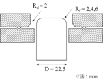
- FIG. 1 is a diagram illustrating a method for evaluating a forming limit in accordance with ISO-12004-2-2008.
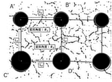
- 13 is a diagram showing the deformation angle and the distance between markings after deformation.
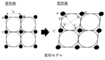
- FIG. FIG. 13 is a diagram showing a method for calculating the maximum strain ⁇ 1 and the minimum strain ⁇ 2 required to calculate VFL.
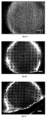
- 1 is a diagram showing an example of a crack penetrating a metal layer;
- electrical conductivity is measured based on the four-probe method defined in JIS K7194.
- the surface of the metal layer may be formed with various surface treatment layers for the purpose of adhesion promotion, environmental resistance, heat resistance, rust prevention, etc.
- various surface treatment layers for the purpose of adhesion promotion, environmental resistance, heat resistance, rust prevention, etc.
- Au plating, Ag plating, Sn plating, Ni plating, Zn plating, Sn alloy plating (Sn-Ag, Sn-Ni, Sn-Cu, etc.), chromate treatment, etc. may be applied. These treatments may be combined. From the viewpoint of cost, Sn plating or Sn alloy plating is preferable.
- chromate treatment, roughening treatment, Ni plating, etc. may be applied.
- metal plating with high relative magnetic permeability may be provided in order to improve the shielding effect against DC magnetic fields.
- Examples of metal plating with high relative magnetic permeability include Fe-Ni alloy plating and Ni plating.
- the purity is preferably 99.5% by mass or more, and more preferably 99.8% by mass or more.
- the copper foil rolled copper foil, electrolytic copper foil, metallized copper foil, etc. can be used, but rolled copper foil, which has excellent flexibility and formability (formability includes drawing formability; the same applies below), is preferable.
- alloy elements are added to the copper foil to make a copper alloy foil, it is preferable that the total content of these elements and unavoidable impurities is less than 0.5% by mass.
- the copper foil contains at least one selected from the group consisting of Sn, Mn, Cr, Zn, Zr, Mg, Ni, Si, and Ag in a total amount of 50 to 2000 ppm by mass, and/or P in a total amount of 10 to 50 ppm by mass, since this improves elongation compared to pure copper foil of the same thickness.
- the thickness of the metal layer constituting the metal-resin composite electromagnetic shielding material according to one embodiment of the present invention is preferably 4 ⁇ m or more per layer. If the thickness is 4 ⁇ m or more, it is possible to avoid the metal layer becoming difficult to handle, and to prevent the ductility of the metal layer from significantly decreasing and the moldability of the laminate from becoming insufficient. In addition, if the thickness of each layer is less than 4 ⁇ m, it becomes necessary to laminate a large number of metal layers in order to obtain an excellent electromagnetic shielding effect, which causes a problem of increased manufacturing costs. From this perspective, the thickness of the metal layer is more preferably 10 ⁇ m or more per layer, even more preferably 12 ⁇ m or more, and even more preferably 15 ⁇ m or more.
- the thickness of the layer is preferably 100 ⁇ m or less per layer, more preferably 50 ⁇ m or less, even more preferably 45 ⁇ m or less, and even more preferably 40 ⁇ m or less.
- the thickness of the metal layer can be measured, for example, by using a constant pressure thickness tester (THICKNESS METER B-1, manufactured by Toyo Seiki Seisakusho) in accordance with Method A of JIS K 6250:2019, and averaging the measured values at four points on the surface of the sheet sample. Note that the measurement can be performed with an indenter diameter of 5 mm and a pressure of 1.22 N applied to the indenter. If the thickness of the metal layer in the laminate is to be measured, it can be measured by observing the thickness cross section with a SEM or the like.
- the metal layer constituting the metal-resin composite electromagnetic shielding material may be a single layer, but from the viewpoint of improving moldability and shielding performance, it is preferable to laminate multiple metal layers constituting the metal-resin composite electromagnetic shielding material with a resin layer interposed therebetween, and from the viewpoint of ensuring excellent electromagnetic shielding properties while reducing the total thickness of the metal-resin composite electromagnetic shielding material, it is more preferable to laminate two or more metal layers with a resin layer interposed therebetween. By laminating two or more metal layers with a resin layer interposed therebetween, the shielding effect is significantly improved compared to when the metal layer is a single layer or when two metal layers are laminated without a resin layer interposed therebetween, even if the total thickness of the metal layers is the same.
- the shielding effect is improved by increasing the total thickness of the metal layers, but in order to obtain a significant improvement effect, it is preferable to laminate the metal layers with a resin layer interposed therebetween.
- the total thickness of the metal layers required to obtain the same electromagnetic shielding effect can be reduced, making it possible to achieve both weight reduction and electromagnetic shielding effect of the laminate.
- the number of metal layers that make up the metal-resin composite electromagnetic wave shielding material is preferably 5 or less, more preferably 4 or less, and even more preferably 3 or less.
- all the metal layers when multiple metal layers are formed, all the metal layers may be made of the same material, or different materials may be used for each layer. In addition, all the metal layers may be of the same thickness, or the thickness may vary from layer to layer.
- the total thickness of all metal layers can be 15 to 150 ⁇ m, or it can be 100 ⁇ m or less, 80 ⁇ m or less, or 60 ⁇ m or less.
- a resin layer is sandwiched between metal layers, and thus a significant improvement in the electromagnetic shielding effect is obtained by stacking a plurality of metal layers.
- the shielding effect is improved by increasing the total thickness of the metal layers even when the metal layers are directly stacked, in order to obtain a significant improvement effect, it is preferable to stack the metal layers via a resin layer. This is thought to be because the presence of a resin layer between the metal layers increases the number of reflections of the electromagnetic waves, thereby attenuating the electromagnetic waves.
- the resin layer In order to obtain an excellent electromagnetic shielding effect, it is preferable for the resin layer to have a large impedance difference with the metal layer.
- the resin layer needs to have a small relative dielectric constant, which is preferably 10.0 (value at 20°C; the same applies below) or less, more preferably 5.0 or less, and even more preferably 3.5 or less.
- the relative dielectric constant cannot be less than 1.0.
- the lowest is around 2.0, and even if it is lowered further to approach 1.0, the increase in shielding effect is limited, while the material itself becomes specialized and expensive.
- the relative dielectric constant is preferably 2.0 or more, and more preferably 2.2 or more.
- synthetic resins are particularly preferred as materials constituting the resin layer.
- Fiber reinforcement materials such as carbon fiber, glass fiber, and aramid fiber can also be mixed into the resin layer.
- magnetic materials may be mixed into the resin layer to the extent that they do not affect the present invention.
- polyesters such as PET (polyethylene terephthalate), PEN (polyethylene naphthalate), and PBT (polybutylene terephthalate), olefin resins such as polyethylene and polypropylene, polyamides, polyimides, liquid crystal polymers, polyacetal, fluororesins, polyurethanes, acrylic resins, epoxy resins, silicone resins, phenolic resins, melamine resins, ABS resins, polyvinyl alcohol, urea resins, polyvinyl chloride, polycarbonates, polystyrene, styrene butadiene rubber, etc. are listed.
- the synthetic resin may be an elastomer such as urethane rubber, chloroprene rubber, silicone rubber, fluororubber, styrene-based, olefin-based, PVC-based, urethane-based, or amide-based.
- the resin layers used in the metal-resin composite electromagnetic shielding material according to one embodiment of the present invention may all be made of the same resin material, or different resin materials may be used for each layer. From the viewpoint of moldability, it is preferable that some or all of the resin layers are insulating layers.
- the resin material can be laminated in the form of a film or fiber.
- the resin layer can also be formed by applying an uncured resin composition to the metal layer and then curing it, but it is preferable to use a resin film that can be attached to the metal layer for ease of production.
- a PET film can be suitably used.
- the strength of the shielding material can be increased by using a biaxially stretched film as the PET film.
- the thickness of the resin layer is not particularly limited, but since the (elongation) breaking strain of the shielding material tends to decrease when the thickness of each layer is thinner than 4 ⁇ m, the thickness of each resin layer is preferably 4 ⁇ m or more, more preferably 7 ⁇ m or more, even more preferably 9 ⁇ m or more, even more preferably 10 ⁇ m or more, even more preferably 20 ⁇ m or more, even more preferably 40 ⁇ m or more, even more preferably 80 ⁇ m or more, and even more preferably 100 ⁇ m or more. On the other hand, even if the thickness of each layer exceeds 600 ⁇ m, the (elongation) breaking strain of the shielding material tends to decrease.
- the thickness of each resin layer is preferably 600 ⁇ m or less, more preferably 500 ⁇ m or less, even more preferably 400 ⁇ m or less, even more preferably 250 ⁇ m or less, and even more preferably 200 ⁇ m or less.
- all the resin layers may have the same thickness, or the thickness may differ from layer to layer.
- one resin layer means a portion where the resin is continuous without a metal layer being interposed. For example, even if multiple resin films are continuously laminated during the manufacturing process of the electromagnetic wave shielding material, there is no metal layer between these films, and since they appear to be one continuous body, they are considered to be one resin layer.
- the thickness of the resin layer can be measured in the same manner as the method for measuring the thickness of the metal layer described above.
- resin layers have higher ductility than metal layers. For this reason, by supporting both sides of each metal layer with a resin layer, the ductility of the shielding metal layer is significantly improved, and the moldability of the laminate is significantly improved. From the viewpoint of improving moldability, it is preferable to stack the metal layers via a resin layer rather than stacking the metal layers directly on top of each other.
- the surface of the resin layer may be subjected to various surface treatments for the purpose of promoting adhesion with the metal layer.
- the adhesion with the shielding metal layer can be improved by applying a primer coat or corona treatment to the bonding surface of the resin layer with the shielding metal layer.
- a metal-resin composite electromagnetic shielding material comprising N (where N is an integer of 1 or more) metal layers and M (where M is an integer of 1 or more) resin layers laminated together, wherein the Value of Forming Limit (VFL) calculated from the following formula satisfies VFL > 0.24:
- N is not particularly limited as long as it is an integer of 1 or more, and a higher electromagnetic shielding effect can be obtained by increasing N.
- N is typically 1, 2, 3, 4, or 5.
- VFL The method for calculating VFL is explained in detail below. The inventors have found that the larger the VFL calculated from the above formula, the higher the moldability.
- the forming limit is evaluated using a mold for FLD (forming limit diagram) ( Figure 1).
- the mold is designed by reducing the size described in ISO-12004-2-2008 by 25%.
- the die R part R d 2 mm.
- the clearance between the punch and the die is 2.25 mm.
- the blank holder is provided with a W-shaped notch, and the mold pressure is set to 4000 N as the initial pressure to prevent the test piece from being pulled in during forming.
- a drive plate is sandwiched between the test piece and the stripper plate to reduce the effects of material and friction. Nitto Denko Corporation's Nitoflon No.
- the drive plate has an outer diameter of ⁇ 60 mm and a hole of ⁇ 2 mm in the center.
- a circular test piece with a diameter of 60 mm is cut out, a grid-like marking with a pitch of 1 mm is applied near the center, and the punch extrusion depth is increased by 0.5 mm to form the test piece.
- Three test pieces are prepared for each depth, and four arbitrary masses of the grid near the center of each test piece are observed with a microscope, and the punch extrusion depth when cracks penetrating the metal layer are observed in 50% or more (i.e., six or more of a total of twelve observation points) is recorded. Then, the size (L 1 , L 2 , L 3 , L 4 ) and deformation angle ( ⁇ 1 , ⁇ 2 ) of each mass at the punch extrusion depth are measured with a microscope (FIG. 2).
- true strains ⁇ 1 and ⁇ 2 corresponding to the maximum and minimum strains in the mass are calculated based on the average length and average deformation angle.
- Finding l 1 ' and l 2 ' from ⁇ 1,2 gives the following: l 1 ' and l 2 ' denote the maximum and minimum diameters of the ellipse.
- the true strain is expressed as follows: The larger of the calculated values is the maximum strain, and the smaller is the minimum strain.
- the maximum depth d at which the crack penetrating the metal layer was less than 50% was defined as the forming limit, and the VFL (Value of Forming Limit) for each mass was calculated from the following formula: In order to reduce measurement variation, the calculated VFLs for each mass were averaged to obtain the VFL for the test piece.
- a crack that penetrates a metal layer means a crack that penetrates the outermost metal layer when the metal layer is the outermost layer (Fig. 4(A)), and when the metal layer is not the outermost layer but is covered with a resin layer, it means that when the resin layer is peeled off, a crack that penetrates the inner metal layer closest to the resin layer is confirmed (Fig. 4(B)).
- Fig. 4(C) When both the resin layer and the metal layer are cracked, even if no cracks have occurred in the metal layer in the four observed squares, it is considered that there are cracks that penetrate the metal layer in all squares (Fig. 4(C)).
- the molding limit of the metal-resin composite electromagnetic shielding material is 5.0 mm or more, and that the molding processability is high. Therefore, when the VFL exceeds 0.24, it is possible to mold it as a continuum, and it is possible to follow irregularities of, for example, 5 mm or more.
- the VFL is preferably 0.26 or more, more preferably 0.28 or more, even more preferably 0.30 or more, even more preferably 0.32 or more, even more preferably 0.34 or more, even more preferably 0.36 or more, even more preferably 0.38 or more, and even more preferably 0.40 or more.
- the upper limit of VFL can be set to 0.50 or less, for example, from the viewpoint of productivity and cost.
- the metal-resin composite electromagnetic shielding material according to each embodiment of the present invention can be used for various electromagnetic shielding applications, such as covering or exterior materials for electrical and electronic devices (e.g., inverters, communication devices, resonators, electron tubes and discharge lamps, electric heating devices, electric motors, generators, electronic components, printed circuits, medical devices, etc.), covering materials for harnesses and communication cables connected to electrical and electronic devices, electromagnetic shielding sheets, electromagnetic shielding panels, electromagnetic shielding bags, electromagnetic shielding boxes, and electromagnetic shielding rooms. It is also possible to insert mold the metal-resin composite electromagnetic shielding material according to each embodiment of the present invention as an insert part. Furthermore, in order to improve the electromagnetic shielding effect, an electromagnetic shielding sheet such as a magnetic sheet can be attached to the inside and/or outside of the metal-resin composite electromagnetic shielding material according to the present invention, as long as it does not affect the present invention.
- electrical and electronic devices e.g., inverters, communication devices, resonators, electron tubes and discharge lamps, electric
- Three types of rolled copper foil (type A: crystal grain size 300 ⁇ m or more; type B: crystal grain size 10 ⁇ m or more; type C: crystal grain size less than 10 ⁇ m when measured from the surface using EBSD (crystal orientation analysis)) and two types of aluminum foil (type A: A8021 material; type B: A8021 material annealed at 300°C for 1 hour) were prepared as the metal layer, and three types of resin (PET: polyethylene terephthalate film, PE: polyethylene film, PC: polycarbonate film) were prepared as the resin layer.
- the thickness and conductivity of the various copper foils and the thickness of the various resins are as shown in Table 1.
- Table 1 the "Filler” column indicates that no filler has been added, and that the "O" indicates that the resin has filler added.
- the apparent conductance C ⁇ ⁇ d (S) was calculated from the conductivity ⁇ (S / m) of the metal layer and the total thickness d (m).
- the conductivity of the metal layer was obtained by the above-mentioned four-probe method, and the thickness of the metal layer was measured by the above-mentioned method using a constant pressure thickness tester (THICKNESS METER B-1, manufactured by Toyo Seiki Seisakusho) for each metal layer before lamination with the resin.
- the magnetic field shielding effect at a frequency of 500 kHz was evaluated under room temperature (25 ° C.) conditions using a magnetic field measuring jig of a KEC method shielding effect measuring device (manufactured by Techno Science Co., Ltd., JSE-KEC) and a network analyzer (manufactured by Keysight Technologies, E5080).
- the calculation results of the apparent conductance C and the measurement results of the shielding effect are shown in Table 1. It can be seen that the examples of the present invention were able to maintain the shielding effect while improving the moldability.
- shielding effect marked with “ ⁇ ” means that the shielding effect is 10 dB or more in the 500 kHz frequency band according to the KEC method, and “ ⁇ ” means that the shielding effect is less than 10 dB in the 500 kHz frequency band according to the KEC method.
- the metal-resin composite electromagnetic shielding material of the embodiment of the present invention had excellent moldability due to a VFL exceeding 0.24. In addition, a high level of shielding effect was maintained. As in Example 24, multiple resin films were laminated in succession as resin layers, but the portions without metal layers were combined into a single resin layer.
Landscapes
- Physics & Mathematics (AREA)
- Electromagnetism (AREA)
- Engineering & Computer Science (AREA)
- Microelectronics & Electronic Packaging (AREA)
- Laminated Bodies (AREA)
- Shielding Devices Or Components To Electric Or Magnetic Fields (AREA)
- Aerials With Secondary Devices (AREA)
Priority Applications (5)
| Application Number | Priority Date | Filing Date | Title |
|---|---|---|---|
| CN202380041378.3A CN119213882A (zh) | 2022-10-26 | 2023-09-15 | 金属树脂复合电磁波屏蔽材料 |
| US18/869,000 US20250318095A1 (en) | 2022-10-26 | 2023-09-15 | Metal Resin Composite Electromagnetic Shielding Material |
| KR1020247038619A KR102979434B1 (ko) | 2022-10-26 | 2023-09-15 | 금속 수지 복합 전자파 실드 재료 |
| EP23882282.9A EP4611497A4 (en) | 2022-10-26 | 2023-09-15 | ELECTROMAGNETIC SHIELDING MATERIAL METALLIC RESIN COMPOSITE |
| JP2024521080A JP7567095B2 (ja) | 2022-10-26 | 2023-09-15 | 金属樹脂複合電磁波シールド材料 |
Applications Claiming Priority (2)
| Application Number | Priority Date | Filing Date | Title |
|---|---|---|---|
| JP2022-171776 | 2022-10-26 | ||
| JP2022171776 | 2022-10-26 |
Publications (1)
| Publication Number | Publication Date |
|---|---|
| WO2024090069A1 true WO2024090069A1 (ja) | 2024-05-02 |
Family
ID=90830493
Family Applications (1)
| Application Number | Title | Priority Date | Filing Date |
|---|---|---|---|
| PCT/JP2023/033800 Ceased WO2024090069A1 (ja) | 2022-10-26 | 2023-09-15 | 金属樹脂複合電磁波シールド材料 |
Country Status (7)
| Country | Link |
|---|---|
| US (1) | US20250318095A1 (cg-RX-API-DMAC7.html) |
| EP (1) | EP4611497A4 (cg-RX-API-DMAC7.html) |
| JP (1) | JP7567095B2 (cg-RX-API-DMAC7.html) |
| KR (1) | KR102979434B1 (cg-RX-API-DMAC7.html) |
| CN (1) | CN119213882A (cg-RX-API-DMAC7.html) |
| TW (1) | TWI881497B (cg-RX-API-DMAC7.html) |
| WO (1) | WO2024090069A1 (cg-RX-API-DMAC7.html) |
Cited By (1)
| Publication number | Priority date | Publication date | Assignee | Title |
|---|---|---|---|---|
| WO2026140337A1 (ja) * | 2024-12-27 | 2026-07-02 | Jx金属株式会社 | 電磁波シールド材、被覆材又は外装材及び電気・電子機器 |
Citations (4)
| Publication number | Priority date | Publication date | Assignee | Title |
|---|---|---|---|---|
| JP2011179162A (ja) | 2011-05-27 | 2011-09-15 | Matsuyama Keori Kk | 電磁波シールド織物、電磁波シールドシート、電磁波シールド材及び電磁波シールドケーシング |
| JP4811245B2 (ja) | 2006-11-27 | 2011-11-09 | パナソニック電工株式会社 | 電磁波シールドケース体物品とその製造方法 |
| JP2021055113A (ja) | 2019-05-30 | 2021-04-08 | 東洋紡株式会社 | 電子部品の封止体 |
| JP2022091579A (ja) * | 2020-12-09 | 2022-06-21 | Jx金属株式会社 | 電磁波シールド材 |
Family Cites Families (3)
| Publication number | Priority date | Publication date | Assignee | Title |
|---|---|---|---|---|
| JPS4811245B1 (cg-RX-API-DMAC7.html) | 1969-06-12 | 1973-04-12 | ||
| DE102019131499A1 (de) * | 2019-11-21 | 2021-05-27 | Carl Freudenberg Kg | Flexibles Laminat zur Abschirmung elektromagnetischer Strahlung |
| EP4436326A4 (en) * | 2021-11-15 | 2025-03-19 | JX Metals Corporation | Metal resin composite electromagnetic shielding material |
-
2023
- 2023-09-15 KR KR1020247038619A patent/KR102979434B1/ko active Active
- 2023-09-15 US US18/869,000 patent/US20250318095A1/en active Pending
- 2023-09-15 JP JP2024521080A patent/JP7567095B2/ja active Active
- 2023-09-15 WO PCT/JP2023/033800 patent/WO2024090069A1/ja not_active Ceased
- 2023-09-15 CN CN202380041378.3A patent/CN119213882A/zh active Pending
- 2023-09-15 EP EP23882282.9A patent/EP4611497A4/en active Pending
- 2023-10-18 TW TW112139698A patent/TWI881497B/zh active
Patent Citations (4)
| Publication number | Priority date | Publication date | Assignee | Title |
|---|---|---|---|---|
| JP4811245B2 (ja) | 2006-11-27 | 2011-11-09 | パナソニック電工株式会社 | 電磁波シールドケース体物品とその製造方法 |
| JP2011179162A (ja) | 2011-05-27 | 2011-09-15 | Matsuyama Keori Kk | 電磁波シールド織物、電磁波シールドシート、電磁波シールド材及び電磁波シールドケーシング |
| JP2021055113A (ja) | 2019-05-30 | 2021-04-08 | 東洋紡株式会社 | 電子部品の封止体 |
| JP2022091579A (ja) * | 2020-12-09 | 2022-06-21 | Jx金属株式会社 | 電磁波シールド材 |
Non-Patent Citations (1)
| Title |
|---|
| See also references of EP4611497A4 |
Cited By (1)
| Publication number | Priority date | Publication date | Assignee | Title |
|---|---|---|---|---|
| WO2026140337A1 (ja) * | 2024-12-27 | 2026-07-02 | Jx金属株式会社 | 電磁波シールド材、被覆材又は外装材及び電気・電子機器 |
Also Published As
| Publication number | Publication date |
|---|---|
| KR20250002590A (ko) | 2025-01-07 |
| KR102979434B1 (ko) | 2026-06-18 |
| EP4611497A1 (en) | 2025-09-03 |
| JPWO2024090069A1 (cg-RX-API-DMAC7.html) | 2024-05-02 |
| TW202435696A (zh) | 2024-09-01 |
| EP4611497A4 (en) | 2026-03-04 |
| US20250318095A1 (en) | 2025-10-09 |
| TWI881497B (zh) | 2025-04-21 |
| CN119213882A (zh) | 2024-12-27 |
| JP7567095B2 (ja) | 2024-10-15 |
Similar Documents
| Publication | Publication Date | Title |
|---|---|---|
| JP6379071B2 (ja) | 電磁波シールド材 | |
| JP7008121B1 (ja) | 電磁波シールド材 | |
| JP6278922B2 (ja) | 電磁波シールド材 | |
| KR102135649B1 (ko) | 전자파 실드재 | |
| JP7567095B2 (ja) | 金属樹脂複合電磁波シールド材料 | |
| JP2025065241A (ja) | 金属樹脂複合電磁波シールド材料 | |
| US10272646B2 (en) | Electromagnetic shielding material | |
| JP6557551B2 (ja) | 電磁波シールド材 | |
| JP2023154282A (ja) | 電磁波シールド積層体、被覆材又は外装材、電気・電子機器及び電磁波シールド積層体の製造方法 |
Legal Events
| Date | Code | Title | Description |
|---|---|---|---|
| ENP | Entry into the national phase |
Ref document number: 2024521080 Country of ref document: JP Kind code of ref document: A |
|
| 121 | Ep: the epo has been informed by wipo that ep was designated in this application |
Ref document number: 23882282 Country of ref document: EP Kind code of ref document: A1 |
|
| WWE | Wipo information: entry into national phase |
Ref document number: 202427080756 Country of ref document: IN |
|
| WWE | Wipo information: entry into national phase |
Ref document number: 202380041378.3 Country of ref document: CN |
|
| ENP | Entry into the national phase |
Ref document number: 20247038619 Country of ref document: KR Kind code of ref document: A |
|
| WWE | Wipo information: entry into national phase |
Ref document number: 1020247038619 Country of ref document: KR |
|
| WWP | Wipo information: published in national office |
Ref document number: 202380041378.3 Country of ref document: CN |
|
| WWE | Wipo information: entry into national phase |
Ref document number: 2023882282 Country of ref document: EP |
|
| NENP | Non-entry into the national phase |
Ref country code: DE |
|
| ENP | Entry into the national phase |
Ref document number: 2023882282 Country of ref document: EP Effective date: 20250526 |
|
| WWP | Wipo information: published in national office |
Ref document number: 2023882282 Country of ref document: EP |
|
| WWP | Wipo information: published in national office |
Ref document number: 18869000 Country of ref document: US |