WO2024089571A1 - Semiconductor device, method for manufacturing semiconductor device, and electronic apparatus - Google Patents
Semiconductor device, method for manufacturing semiconductor device, and electronic apparatus Download PDFInfo
- Publication number
- WO2024089571A1 WO2024089571A1 PCT/IB2023/060659 IB2023060659W WO2024089571A1 WO 2024089571 A1 WO2024089571 A1 WO 2024089571A1 IB 2023060659 W IB2023060659 W IB 2023060659W WO 2024089571 A1 WO2024089571 A1 WO 2024089571A1
- Authority
- WO
- WIPO (PCT)
- Prior art keywords
- layer
- conductive layer
- insulating layer
- region
- semiconductor
- Prior art date
Links
- 239000004065 semiconductor Substances 0.000 title claims abstract description 615
- 238000000034 method Methods 0.000 title claims description 249
- 238000004519 manufacturing process Methods 0.000 title claims description 109
- 150000004706 metal oxides Chemical class 0.000 claims description 198
- 229910044991 metal oxide Inorganic materials 0.000 claims description 197
- 229910052760 oxygen Inorganic materials 0.000 claims description 114
- 239000001301 oxygen Substances 0.000 claims description 113
- QVGXLLKOCUKJST-UHFFFAOYSA-N atomic oxygen Chemical compound [O] QVGXLLKOCUKJST-UHFFFAOYSA-N 0.000 claims description 109
- 230000015572 biosynthetic process Effects 0.000 claims description 100
- 239000000463 material Substances 0.000 claims description 98
- IJGRMHOSHXDMSA-UHFFFAOYSA-N Atomic nitrogen Chemical compound N#N IJGRMHOSHXDMSA-UHFFFAOYSA-N 0.000 claims description 84
- 238000011282 treatment Methods 0.000 claims description 73
- XUIMIQQOPSSXEZ-UHFFFAOYSA-N Silicon Chemical compound [Si] XUIMIQQOPSSXEZ-UHFFFAOYSA-N 0.000 claims description 61
- 229910052710 silicon Inorganic materials 0.000 claims description 61
- 239000010703 silicon Substances 0.000 claims description 61
- 230000003647 oxidation Effects 0.000 claims description 46
- 238000007254 oxidation reaction Methods 0.000 claims description 46
- 229910052757 nitrogen Inorganic materials 0.000 claims description 40
- 238000012545 processing Methods 0.000 claims description 39
- 239000011701 zinc Substances 0.000 claims description 38
- 229910052782 aluminium Inorganic materials 0.000 claims description 30
- XAGFODPZIPBFFR-UHFFFAOYSA-N aluminium Chemical compound [Al] XAGFODPZIPBFFR-UHFFFAOYSA-N 0.000 claims description 30
- 238000005530 etching Methods 0.000 claims description 28
- WFKWXMTUELFFGS-UHFFFAOYSA-N tungsten Chemical compound [W] WFKWXMTUELFFGS-UHFFFAOYSA-N 0.000 claims description 23
- 229910052721 tungsten Inorganic materials 0.000 claims description 23
- 239000010937 tungsten Substances 0.000 claims description 23
- VBJZVLUMGGDVMO-UHFFFAOYSA-N hafnium atom Chemical compound [Hf] VBJZVLUMGGDVMO-UHFFFAOYSA-N 0.000 claims description 21
- 229910052735 hafnium Inorganic materials 0.000 claims description 20
- APFVFJFRJDLVQX-UHFFFAOYSA-N indium atom Chemical compound [In] APFVFJFRJDLVQX-UHFFFAOYSA-N 0.000 claims description 20
- GYHNNYVSQQEPJS-UHFFFAOYSA-N Gallium Chemical compound [Ga] GYHNNYVSQQEPJS-UHFFFAOYSA-N 0.000 claims description 19
- 229910052733 gallium Inorganic materials 0.000 claims description 19
- 229910052738 indium Inorganic materials 0.000 claims description 19
- PXHVJJICTQNCMI-UHFFFAOYSA-N Nickel Chemical compound [Ni] PXHVJJICTQNCMI-UHFFFAOYSA-N 0.000 claims description 14
- 239000010936 titanium Substances 0.000 claims description 13
- RTAQQCXQSZGOHL-UHFFFAOYSA-N Titanium Chemical compound [Ti] RTAQQCXQSZGOHL-UHFFFAOYSA-N 0.000 claims description 12
- 229910052796 boron Inorganic materials 0.000 claims description 12
- 229910052746 lanthanum Inorganic materials 0.000 claims description 12
- FZLIPJUXYLNCLC-UHFFFAOYSA-N lanthanum atom Chemical compound [La] FZLIPJUXYLNCLC-UHFFFAOYSA-N 0.000 claims description 12
- 229910052715 tantalum Inorganic materials 0.000 claims description 12
- GUVRBAGPIYLISA-UHFFFAOYSA-N tantalum atom Chemical compound [Ta] GUVRBAGPIYLISA-UHFFFAOYSA-N 0.000 claims description 12
- 229910052719 titanium Inorganic materials 0.000 claims description 12
- 229910052712 strontium Inorganic materials 0.000 claims description 10
- CIOAGBVUUVVLOB-UHFFFAOYSA-N strontium atom Chemical compound [Sr] CIOAGBVUUVVLOB-UHFFFAOYSA-N 0.000 claims description 10
- ZOXJGFHDIHLPTG-UHFFFAOYSA-N Boron Chemical compound [B] ZOXJGFHDIHLPTG-UHFFFAOYSA-N 0.000 claims description 9
- XEEYBQQBJWHFJM-UHFFFAOYSA-N Iron Chemical compound [Fe] XEEYBQQBJWHFJM-UHFFFAOYSA-N 0.000 claims description 9
- QCWXUUIWCKQGHC-UHFFFAOYSA-N Zirconium Chemical compound [Zr] QCWXUUIWCKQGHC-UHFFFAOYSA-N 0.000 claims description 9
- 229910052727 yttrium Inorganic materials 0.000 claims description 9
- VWQVUPCCIRVNHF-UHFFFAOYSA-N yttrium atom Chemical compound [Y] VWQVUPCCIRVNHF-UHFFFAOYSA-N 0.000 claims description 9
- ZOKXTWBITQBERF-UHFFFAOYSA-N Molybdenum Chemical compound [Mo] ZOKXTWBITQBERF-UHFFFAOYSA-N 0.000 claims description 8
- 229910052750 molybdenum Inorganic materials 0.000 claims description 8
- 239000011733 molybdenum Substances 0.000 claims description 8
- 229910052726 zirconium Inorganic materials 0.000 claims description 8
- FYYHWMGAXLPEAU-UHFFFAOYSA-N Magnesium Chemical compound [Mg] FYYHWMGAXLPEAU-UHFFFAOYSA-N 0.000 claims description 7
- 229910052779 Neodymium Inorganic materials 0.000 claims description 7
- ATJFFYVFTNAWJD-UHFFFAOYSA-N Tin Chemical compound [Sn] ATJFFYVFTNAWJD-UHFFFAOYSA-N 0.000 claims description 7
- HCHKCACWOHOZIP-UHFFFAOYSA-N Zinc Chemical compound [Zn] HCHKCACWOHOZIP-UHFFFAOYSA-N 0.000 claims description 7
- 229910052732 germanium Inorganic materials 0.000 claims description 7
- GNPVGFCGXDBREM-UHFFFAOYSA-N germanium atom Chemical compound [Ge] GNPVGFCGXDBREM-UHFFFAOYSA-N 0.000 claims description 7
- 229910052749 magnesium Inorganic materials 0.000 claims description 7
- 239000011777 magnesium Substances 0.000 claims description 7
- QEFYFXOXNSNQGX-UHFFFAOYSA-N neodymium atom Chemical compound [Nd] QEFYFXOXNSNQGX-UHFFFAOYSA-N 0.000 claims description 7
- 229910052759 nickel Inorganic materials 0.000 claims description 7
- 229910052718 tin Inorganic materials 0.000 claims description 7
- 229910052684 Cerium Inorganic materials 0.000 claims description 6
- 229910052725 zinc Inorganic materials 0.000 claims description 6
- VYZAMTAEIAYCRO-UHFFFAOYSA-N Chromium Chemical compound [Cr] VYZAMTAEIAYCRO-UHFFFAOYSA-N 0.000 claims description 5
- 229910052787 antimony Inorganic materials 0.000 claims description 5
- WATWJIUSRGPENY-UHFFFAOYSA-N antimony atom Chemical compound [Sb] WATWJIUSRGPENY-UHFFFAOYSA-N 0.000 claims description 5
- 229910052788 barium Inorganic materials 0.000 claims description 5
- DSAJWYNOEDNPEQ-UHFFFAOYSA-N barium atom Chemical compound [Ba] DSAJWYNOEDNPEQ-UHFFFAOYSA-N 0.000 claims description 5
- 229910052804 chromium Inorganic materials 0.000 claims description 5
- 239000011651 chromium Substances 0.000 claims description 5
- WPBNNNQJVZRUHP-UHFFFAOYSA-L manganese(2+);methyl n-[[2-(methoxycarbonylcarbamothioylamino)phenyl]carbamothioyl]carbamate;n-[2-(sulfidocarbothioylamino)ethyl]carbamodithioate Chemical compound [Mn+2].[S-]C(=S)NCCNC([S-])=S.COC(=O)NC(=S)NC1=CC=CC=C1NC(=S)NC(=O)OC WPBNNNQJVZRUHP-UHFFFAOYSA-L 0.000 claims description 5
- 229910052720 vanadium Inorganic materials 0.000 claims description 5
- OYPRJOBELJOOCE-UHFFFAOYSA-N Calcium Chemical compound [Ca] OYPRJOBELJOOCE-UHFFFAOYSA-N 0.000 claims description 4
- 229910052791 calcium Inorganic materials 0.000 claims description 4
- 239000011575 calcium Substances 0.000 claims description 4
- 229910017052 cobalt Inorganic materials 0.000 claims description 4
- 239000010941 cobalt Substances 0.000 claims description 4
- GUTLYIVDDKVIGB-UHFFFAOYSA-N cobalt atom Chemical compound [Co] GUTLYIVDDKVIGB-UHFFFAOYSA-N 0.000 claims description 4
- 229910052742 iron Inorganic materials 0.000 claims description 4
- GWXLDORMOJMVQZ-UHFFFAOYSA-N cerium Chemical compound [Ce] GWXLDORMOJMVQZ-UHFFFAOYSA-N 0.000 claims 2
- LEONUFNNVUYDNQ-UHFFFAOYSA-N vanadium atom Chemical compound [V] LEONUFNNVUYDNQ-UHFFFAOYSA-N 0.000 claims 2
- 239000010410 layer Substances 0.000 abstract description 1895
- 230000006870 function Effects 0.000 abstract description 162
- 239000011229 interlayer Substances 0.000 abstract description 43
- 230000002349 favourable effect Effects 0.000 abstract description 2
- 230000015654 memory Effects 0.000 description 252
- 239000010408 film Substances 0.000 description 164
- 239000000758 substrate Substances 0.000 description 95
- 239000012212 insulator Substances 0.000 description 69
- 239000004020 conductor Substances 0.000 description 64
- 238000003860 storage Methods 0.000 description 63
- 239000012535 impurity Substances 0.000 description 57
- 229910052751 metal Inorganic materials 0.000 description 56
- 239000001257 hydrogen Substances 0.000 description 53
- 229910052739 hydrogen Inorganic materials 0.000 description 53
- 239000000203 mixture Substances 0.000 description 52
- UFHFLCQGNIYNRP-UHFFFAOYSA-N Hydrogen Chemical compound [H][H] UFHFLCQGNIYNRP-UHFFFAOYSA-N 0.000 description 45
- 230000008569 process Effects 0.000 description 44
- 125000004429 atom Chemical group 0.000 description 43
- 238000000231 atomic layer deposition Methods 0.000 description 42
- 239000007789 gas Substances 0.000 description 38
- 239000003990 capacitor Substances 0.000 description 36
- 239000002184 metal Substances 0.000 description 34
- 238000010586 diagram Methods 0.000 description 33
- 239000013078 crystal Substances 0.000 description 32
- 238000010438 heat treatment Methods 0.000 description 32
- 238000004544 sputter deposition Methods 0.000 description 28
- 238000005229 chemical vapour deposition Methods 0.000 description 27
- 230000007547 defect Effects 0.000 description 26
- 229910052799 carbon Inorganic materials 0.000 description 24
- VYPSYNLAJGMNEJ-UHFFFAOYSA-N Silicium dioxide Chemical compound O=[Si]=O VYPSYNLAJGMNEJ-UHFFFAOYSA-N 0.000 description 22
- 229910052814 silicon oxide Inorganic materials 0.000 description 22
- 239000000523 sample Substances 0.000 description 21
- 239000002356 single layer Substances 0.000 description 20
- 150000004767 nitrides Chemical class 0.000 description 19
- TWNQGVIAIRXVLR-UHFFFAOYSA-N oxo(oxoalumanyloxy)alumane Chemical compound O=[Al]O[Al]=O TWNQGVIAIRXVLR-UHFFFAOYSA-N 0.000 description 19
- 230000000694 effects Effects 0.000 description 18
- XLYOFNOQVPJJNP-UHFFFAOYSA-N water Substances O XLYOFNOQVPJJNP-UHFFFAOYSA-N 0.000 description 18
- OKTJSMMVPCPJKN-UHFFFAOYSA-N Carbon Chemical compound [C] OKTJSMMVPCPJKN-UHFFFAOYSA-N 0.000 description 17
- XLOMVQKBTHCTTD-UHFFFAOYSA-N Zinc monoxide Chemical compound [Zn]=O XLOMVQKBTHCTTD-UHFFFAOYSA-N 0.000 description 17
- 238000001312 dry etching Methods 0.000 description 17
- 230000004888 barrier function Effects 0.000 description 16
- 230000003071 parasitic effect Effects 0.000 description 16
- 229910052581 Si3N4 Inorganic materials 0.000 description 15
- 238000003491 array Methods 0.000 description 15
- HQVNEWCFYHHQES-UHFFFAOYSA-N silicon nitride Chemical compound N12[Si]34N5[Si]62N3[Si]51N64 HQVNEWCFYHHQES-UHFFFAOYSA-N 0.000 description 15
- -1 silicon oxide Chemical compound 0.000 description 14
- AMGQUBHHOARCQH-UHFFFAOYSA-N indium;oxotin Chemical compound [In].[Sn]=O AMGQUBHHOARCQH-UHFFFAOYSA-N 0.000 description 13
- 230000002093 peripheral effect Effects 0.000 description 13
- NRTOMJZYCJJWKI-UHFFFAOYSA-N Titanium nitride Chemical compound [Ti]#N NRTOMJZYCJJWKI-UHFFFAOYSA-N 0.000 description 12
- 239000002346 layers by function Substances 0.000 description 12
- 239000000126 substance Substances 0.000 description 12
- 238000004364 calculation method Methods 0.000 description 11
- 150000002431 hydrogen Chemical class 0.000 description 10
- 229910045601 alloy Inorganic materials 0.000 description 9
- 239000000956 alloy Substances 0.000 description 9
- 239000000969 carrier Substances 0.000 description 9
- 238000009792 diffusion process Methods 0.000 description 9
- 229910000449 hafnium oxide Inorganic materials 0.000 description 9
- WIHZLLGSGQNAGK-UHFFFAOYSA-N hafnium(4+);oxygen(2-) Chemical compound [O-2].[O-2].[Hf+4] WIHZLLGSGQNAGK-UHFFFAOYSA-N 0.000 description 9
- 239000011810 insulating material Substances 0.000 description 9
- 238000001004 secondary ion mass spectrometry Methods 0.000 description 9
- MZLGASXMSKOWSE-UHFFFAOYSA-N tantalum nitride Chemical compound [Ta]#N MZLGASXMSKOWSE-UHFFFAOYSA-N 0.000 description 9
- 238000001039 wet etching Methods 0.000 description 9
- 239000011787 zinc oxide Substances 0.000 description 9
- XKRFYHLGVUSROY-UHFFFAOYSA-N Argon Chemical compound [Ar] XKRFYHLGVUSROY-UHFFFAOYSA-N 0.000 description 8
- RVTZCBVAJQQJTK-UHFFFAOYSA-N oxygen(2-);zirconium(4+) Chemical compound [O-2].[O-2].[Zr+4] RVTZCBVAJQQJTK-UHFFFAOYSA-N 0.000 description 8
- 230000005855 radiation Effects 0.000 description 8
- 229910001928 zirconium oxide Inorganic materials 0.000 description 8
- MYMOFIZGZYHOMD-UHFFFAOYSA-N Dioxygen Chemical compound O=O MYMOFIZGZYHOMD-UHFFFAOYSA-N 0.000 description 7
- 230000008859 change Effects 0.000 description 7
- AJNVQOSZGJRYEI-UHFFFAOYSA-N digallium;oxygen(2-) Chemical compound [O-2].[O-2].[O-2].[Ga+3].[Ga+3] AJNVQOSZGJRYEI-UHFFFAOYSA-N 0.000 description 7
- 229910001195 gallium oxide Inorganic materials 0.000 description 7
- 238000001459 lithography Methods 0.000 description 7
- 239000002243 precursor Substances 0.000 description 7
- ZAMOUSCENKQFHK-UHFFFAOYSA-N Chlorine atom Chemical compound [Cl] ZAMOUSCENKQFHK-UHFFFAOYSA-N 0.000 description 6
- RYGMFSIKBFXOCR-UHFFFAOYSA-N Copper Chemical compound [Cu] RYGMFSIKBFXOCR-UHFFFAOYSA-N 0.000 description 6
- 238000004833 X-ray photoelectron spectroscopy Methods 0.000 description 6
- 238000004458 analytical method Methods 0.000 description 6
- 238000013473 artificial intelligence Methods 0.000 description 6
- 238000006243 chemical reaction Methods 0.000 description 6
- 229910052801 chlorine Inorganic materials 0.000 description 6
- 239000000460 chlorine Substances 0.000 description 6
- 230000007423 decrease Effects 0.000 description 6
- 230000005684 electric field Effects 0.000 description 6
- 229910003437 indium oxide Inorganic materials 0.000 description 6
- PJXISJQVUVHSOJ-UHFFFAOYSA-N indium(iii) oxide Chemical compound [O-2].[O-2].[O-2].[In+3].[In+3] PJXISJQVUVHSOJ-UHFFFAOYSA-N 0.000 description 6
- 230000010354 integration Effects 0.000 description 6
- 239000011159 matrix material Substances 0.000 description 6
- 229910052707 ruthenium Inorganic materials 0.000 description 6
- 238000002230 thermal chemical vapour deposition Methods 0.000 description 6
- YVTHLONGBIQYBO-UHFFFAOYSA-N zinc indium(3+) oxygen(2-) Chemical compound [O--].[Zn++].[In+3] YVTHLONGBIQYBO-UHFFFAOYSA-N 0.000 description 6
- VUFNLQXQSDUXKB-DOFZRALJSA-N 2-[4-[4-[bis(2-chloroethyl)amino]phenyl]butanoyloxy]ethyl (5z,8z,11z,14z)-icosa-5,8,11,14-tetraenoate Chemical group CCCCC\C=C/C\C=C/C\C=C/C\C=C/CCCC(=O)OCCOC(=O)CCCC1=CC=C(N(CCCl)CCCl)C=C1 VUFNLQXQSDUXKB-DOFZRALJSA-N 0.000 description 5
- OAICVXFJPJFONN-UHFFFAOYSA-N Phosphorus Chemical compound [P] OAICVXFJPJFONN-UHFFFAOYSA-N 0.000 description 5
- KJTLSVCANCCWHF-UHFFFAOYSA-N Ruthenium Chemical compound [Ru] KJTLSVCANCCWHF-UHFFFAOYSA-N 0.000 description 5
- GWEVSGVZZGPLCZ-UHFFFAOYSA-N Titan oxide Chemical compound O=[Ti]=O GWEVSGVZZGPLCZ-UHFFFAOYSA-N 0.000 description 5
- 230000005540 biological transmission Effects 0.000 description 5
- 150000001875 compounds Chemical class 0.000 description 5
- 229910052802 copper Inorganic materials 0.000 description 5
- 239000010949 copper Substances 0.000 description 5
- 229910001873 dinitrogen Inorganic materials 0.000 description 5
- 229910001882 dioxygen Inorganic materials 0.000 description 5
- 230000005621 ferroelectricity Effects 0.000 description 5
- 230000005669 field effect Effects 0.000 description 5
- CPLXHLVBOLITMK-UHFFFAOYSA-N magnesium oxide Inorganic materials [Mg]=O CPLXHLVBOLITMK-UHFFFAOYSA-N 0.000 description 5
- 239000000395 magnesium oxide Substances 0.000 description 5
- AXZKOIWUVFPNLO-UHFFFAOYSA-N magnesium;oxygen(2-) Chemical compound [O-2].[Mg+2] AXZKOIWUVFPNLO-UHFFFAOYSA-N 0.000 description 5
- 229910052698 phosphorus Inorganic materials 0.000 description 5
- 239000011574 phosphorus Substances 0.000 description 5
- 229910021420 polycrystalline silicon Inorganic materials 0.000 description 5
- 229920005989 resin Polymers 0.000 description 5
- 239000011347 resin Substances 0.000 description 5
- OGIDPMRJRNCKJF-UHFFFAOYSA-N titanium oxide Inorganic materials [Ti]=O OGIDPMRJRNCKJF-UHFFFAOYSA-N 0.000 description 5
- 229910052723 transition metal Inorganic materials 0.000 description 5
- CURLTUGMZLYLDI-UHFFFAOYSA-N Carbon dioxide Chemical compound O=C=O CURLTUGMZLYLDI-UHFFFAOYSA-N 0.000 description 4
- PXGOKWXKJXAPGV-UHFFFAOYSA-N Fluorine Chemical compound FF PXGOKWXKJXAPGV-UHFFFAOYSA-N 0.000 description 4
- 101001094647 Homo sapiens Serum paraoxonase/arylesterase 1 Proteins 0.000 description 4
- 101000621061 Homo sapiens Serum paraoxonase/arylesterase 2 Proteins 0.000 description 4
- 102100035476 Serum paraoxonase/arylesterase 1 Human genes 0.000 description 4
- 102100022824 Serum paraoxonase/arylesterase 2 Human genes 0.000 description 4
- 229910052784 alkaline earth metal Inorganic materials 0.000 description 4
- 229910052786 argon Inorganic materials 0.000 description 4
- ZMIGMASIKSOYAM-UHFFFAOYSA-N cerium Chemical compound [Ce][Ce][Ce][Ce][Ce][Ce][Ce][Ce][Ce][Ce][Ce][Ce][Ce][Ce][Ce][Ce][Ce][Ce][Ce][Ce][Ce][Ce][Ce][Ce][Ce][Ce][Ce][Ce][Ce][Ce][Ce][Ce][Ce][Ce][Ce][Ce][Ce][Ce] ZMIGMASIKSOYAM-UHFFFAOYSA-N 0.000 description 4
- 150000004770 chalcogenides Chemical class 0.000 description 4
- 239000000470 constituent Substances 0.000 description 4
- 238000000151 deposition Methods 0.000 description 4
- 229910052731 fluorine Inorganic materials 0.000 description 4
- 239000011737 fluorine Substances 0.000 description 4
- 230000020169 heat generation Effects 0.000 description 4
- QGLKJKCYBOYXKC-UHFFFAOYSA-N nonaoxidotritungsten Chemical compound O=[W]1(=O)O[W](=O)(=O)O[W](=O)(=O)O1 QGLKJKCYBOYXKC-UHFFFAOYSA-N 0.000 description 4
- 230000001590 oxidative effect Effects 0.000 description 4
- 125000004430 oxygen atom Chemical group O* 0.000 description 4
- BPUBBGLMJRNUCC-UHFFFAOYSA-N oxygen(2-);tantalum(5+) Chemical compound [O-2].[O-2].[O-2].[O-2].[O-2].[Ta+5].[Ta+5] BPUBBGLMJRNUCC-UHFFFAOYSA-N 0.000 description 4
- 239000000376 reactant Substances 0.000 description 4
- 230000004044 response Effects 0.000 description 4
- 229910001936 tantalum oxide Inorganic materials 0.000 description 4
- 239000010409 thin film Substances 0.000 description 4
- 229910001930 tungsten oxide Inorganic materials 0.000 description 4
- 229910018137 Al-Zn Inorganic materials 0.000 description 3
- 229910018573 Al—Zn Inorganic materials 0.000 description 3
- MWUXSHHQAYIFBG-UHFFFAOYSA-N Nitric oxide Chemical compound O=[N] MWUXSHHQAYIFBG-UHFFFAOYSA-N 0.000 description 3
- 230000009471 action Effects 0.000 description 3
- 229910052783 alkali metal Inorganic materials 0.000 description 3
- 150000001340 alkali metals Chemical class 0.000 description 3
- 150000001342 alkaline earth metals Chemical class 0.000 description 3
- 239000002585 base Substances 0.000 description 3
- 238000004891 communication Methods 0.000 description 3
- PMHQVHHXPFUNSP-UHFFFAOYSA-M copper(1+);methylsulfanylmethane;bromide Chemical compound Br[Cu].CSC PMHQVHHXPFUNSP-UHFFFAOYSA-M 0.000 description 3
- 238000013461 design Methods 0.000 description 3
- 238000005516 engineering process Methods 0.000 description 3
- YZZNJYQZJKSEER-UHFFFAOYSA-N gallium tin Chemical compound [Ga].[Sn] YZZNJYQZJKSEER-UHFFFAOYSA-N 0.000 description 3
- KQHQLIAOAVMAOW-UHFFFAOYSA-N hafnium(4+) oxygen(2-) zirconium(4+) Chemical compound [O--].[O--].[O--].[O--].[Zr+4].[Hf+4] KQHQLIAOAVMAOW-UHFFFAOYSA-N 0.000 description 3
- 125000004435 hydrogen atom Chemical group [H]* 0.000 description 3
- 239000011261 inert gas Substances 0.000 description 3
- 239000004615 ingredient Substances 0.000 description 3
- 239000007788 liquid Substances 0.000 description 3
- 238000005259 measurement Methods 0.000 description 3
- 239000002245 particle Substances 0.000 description 3
- 229910001925 ruthenium oxide Inorganic materials 0.000 description 3
- WOCIAKWEIIZHES-UHFFFAOYSA-N ruthenium(iv) oxide Chemical compound O=[Ru]=O WOCIAKWEIIZHES-UHFFFAOYSA-N 0.000 description 3
- 238000005477 sputtering target Methods 0.000 description 3
- 229910052714 tellurium Inorganic materials 0.000 description 3
- PORWMNRCUJJQNO-UHFFFAOYSA-N tellurium atom Chemical compound [Te] PORWMNRCUJJQNO-UHFFFAOYSA-N 0.000 description 3
- 238000012546 transfer Methods 0.000 description 3
- GPPXJZIENCGNKB-UHFFFAOYSA-N vanadium Chemical compound [V]#[V] GPPXJZIENCGNKB-UHFFFAOYSA-N 0.000 description 3
- JBRZTFJDHDCESZ-UHFFFAOYSA-N AsGa Chemical compound [As]#[Ga] JBRZTFJDHDCESZ-UHFFFAOYSA-N 0.000 description 2
- 229910052582 BN Inorganic materials 0.000 description 2
- PZNSFCLAULLKQX-UHFFFAOYSA-N Boron nitride Chemical compound N#B PZNSFCLAULLKQX-UHFFFAOYSA-N 0.000 description 2
- WKBOTKDWSSQWDR-UHFFFAOYSA-N Bromine atom Chemical compound [Br] WKBOTKDWSSQWDR-UHFFFAOYSA-N 0.000 description 2
- 229910052693 Europium Inorganic materials 0.000 description 2
- 229910052688 Gadolinium Inorganic materials 0.000 description 2
- 229910001218 Gallium arsenide Inorganic materials 0.000 description 2
- GPXJNWSHGFTCBW-UHFFFAOYSA-N Indium phosphide Chemical compound [In]#P GPXJNWSHGFTCBW-UHFFFAOYSA-N 0.000 description 2
- 229910052777 Praseodymium Inorganic materials 0.000 description 2
- 229910052773 Promethium Inorganic materials 0.000 description 2
- 229910052772 Samarium Inorganic materials 0.000 description 2
- BUGBHKTXTAQXES-UHFFFAOYSA-N Selenium Chemical compound [Se] BUGBHKTXTAQXES-UHFFFAOYSA-N 0.000 description 2
- 229910000577 Silicon-germanium Inorganic materials 0.000 description 2
- BQCADISMDOOEFD-UHFFFAOYSA-N Silver Chemical compound [Ag] BQCADISMDOOEFD-UHFFFAOYSA-N 0.000 description 2
- 229910020994 Sn-Zn Inorganic materials 0.000 description 2
- 229910009069 Sn—Zn Inorganic materials 0.000 description 2
- NINIDFKCEFEMDL-UHFFFAOYSA-N Sulfur Chemical compound [S] NINIDFKCEFEMDL-UHFFFAOYSA-N 0.000 description 2
- BOTDANWDWHJENH-UHFFFAOYSA-N Tetraethyl orthosilicate Chemical compound CCO[Si](OCC)(OCC)OCC BOTDANWDWHJENH-UHFFFAOYSA-N 0.000 description 2
- DBKNIEBLJMAJHX-UHFFFAOYSA-N [As]#B Chemical compound [As]#B DBKNIEBLJMAJHX-UHFFFAOYSA-N 0.000 description 2
- LEVVHYCKPQWKOP-UHFFFAOYSA-N [Si].[Ge] Chemical compound [Si].[Ge] LEVVHYCKPQWKOP-UHFFFAOYSA-N 0.000 description 2
- 238000013528 artificial neural network Methods 0.000 description 2
- 229910052454 barium strontium titanate Inorganic materials 0.000 description 2
- 230000008901 benefit Effects 0.000 description 2
- 229910052797 bismuth Inorganic materials 0.000 description 2
- JCXGWMGPZLAOME-UHFFFAOYSA-N bismuth atom Chemical compound [Bi] JCXGWMGPZLAOME-UHFFFAOYSA-N 0.000 description 2
- ILAHWRKJUDSMFH-UHFFFAOYSA-N boron tribromide Chemical compound BrB(Br)Br ILAHWRKJUDSMFH-UHFFFAOYSA-N 0.000 description 2
- GDTBXPJZTBHREO-UHFFFAOYSA-N bromine Substances BrBr GDTBXPJZTBHREO-UHFFFAOYSA-N 0.000 description 2
- 229910052794 bromium Inorganic materials 0.000 description 2
- 229910002092 carbon dioxide Inorganic materials 0.000 description 2
- 229910052800 carbon group element Inorganic materials 0.000 description 2
- 239000000919 ceramic Substances 0.000 description 2
- 229910052798 chalcogen Inorganic materials 0.000 description 2
- 150000001787 chalcogens Chemical class 0.000 description 2
- 238000013527 convolutional neural network Methods 0.000 description 2
- 230000006866 deterioration Effects 0.000 description 2
- JAONJTDQXUSBGG-UHFFFAOYSA-N dialuminum;dizinc;oxygen(2-) Chemical compound [O-2].[O-2].[O-2].[O-2].[O-2].[Al+3].[Al+3].[Zn+2].[Zn+2] JAONJTDQXUSBGG-UHFFFAOYSA-N 0.000 description 2
- 238000010894 electron beam technology Methods 0.000 description 2
- 238000002003 electron diffraction Methods 0.000 description 2
- 238000002149 energy-dispersive X-ray emission spectroscopy Methods 0.000 description 2
- OGPBJKLSAFTDLK-UHFFFAOYSA-N europium atom Chemical compound [Eu] OGPBJKLSAFTDLK-UHFFFAOYSA-N 0.000 description 2
- UIWYJDYFSGRHKR-UHFFFAOYSA-N gadolinium atom Chemical compound [Gd] UIWYJDYFSGRHKR-UHFFFAOYSA-N 0.000 description 2
- 239000011521 glass Substances 0.000 description 2
- 230000012447 hatching Effects 0.000 description 2
- 238000003384 imaging method Methods 0.000 description 2
- 238000001095 inductively coupled plasma mass spectrometry Methods 0.000 description 2
- 238000002354 inductively-coupled plasma atomic emission spectroscopy Methods 0.000 description 2
- 238000010884 ion-beam technique Methods 0.000 description 2
- MRELNEQAGSRDBK-UHFFFAOYSA-N lanthanum(3+);oxygen(2-) Chemical compound [O-2].[O-2].[O-2].[La+3].[La+3] MRELNEQAGSRDBK-UHFFFAOYSA-N 0.000 description 2
- 229910052451 lead zirconate titanate Inorganic materials 0.000 description 2
- 229910052752 metalloid Inorganic materials 0.000 description 2
- PLDDOISOJJCEMH-UHFFFAOYSA-N neodymium(3+);oxygen(2-) Chemical compound [O-2].[O-2].[O-2].[Nd+3].[Nd+3] PLDDOISOJJCEMH-UHFFFAOYSA-N 0.000 description 2
- RUFLMLWJRZAWLJ-UHFFFAOYSA-N nickel silicide Chemical compound [Ni]=[Si]=[Ni] RUFLMLWJRZAWLJ-UHFFFAOYSA-N 0.000 description 2
- 229910021334 nickel silicide Inorganic materials 0.000 description 2
- 125000004433 nitrogen atom Chemical group N* 0.000 description 2
- 239000012466 permeate Substances 0.000 description 2
- 238000000206 photolithography Methods 0.000 description 2
- 238000005268 plasma chemical vapour deposition Methods 0.000 description 2
- BASFCYQUMIYNBI-UHFFFAOYSA-N platinum Chemical compound [Pt] BASFCYQUMIYNBI-UHFFFAOYSA-N 0.000 description 2
- PUDIUYLPXJFUGB-UHFFFAOYSA-N praseodymium atom Chemical compound [Pr] PUDIUYLPXJFUGB-UHFFFAOYSA-N 0.000 description 2
- VQMWBBYLQSCNPO-UHFFFAOYSA-N promethium atom Chemical compound [Pm] VQMWBBYLQSCNPO-UHFFFAOYSA-N 0.000 description 2
- 238000001552 radio frequency sputter deposition Methods 0.000 description 2
- KZUNJOHGWZRPMI-UHFFFAOYSA-N samarium atom Chemical compound [Sm] KZUNJOHGWZRPMI-UHFFFAOYSA-N 0.000 description 2
- 238000000851 scanning transmission electron micrograph Methods 0.000 description 2
- 238000001350 scanning transmission electron microscopy Methods 0.000 description 2
- 229910052711 selenium Inorganic materials 0.000 description 2
- 239000011669 selenium Substances 0.000 description 2
- 229910021332 silicide Inorganic materials 0.000 description 2
- FVBUAEGBCNSCDD-UHFFFAOYSA-N silicide(4-) Chemical compound [Si-4] FVBUAEGBCNSCDD-UHFFFAOYSA-N 0.000 description 2
- HBMJWWWQQXIZIP-UHFFFAOYSA-N silicon carbide Chemical compound [Si+]#[C-] HBMJWWWQQXIZIP-UHFFFAOYSA-N 0.000 description 2
- 229910010271 silicon carbide Inorganic materials 0.000 description 2
- 229910052709 silver Inorganic materials 0.000 description 2
- 239000004332 silver Substances 0.000 description 2
- 229910000679 solder Inorganic materials 0.000 description 2
- 229910052717 sulfur Inorganic materials 0.000 description 2
- 239000011593 sulfur Substances 0.000 description 2
- VZGDMQKNWNREIO-UHFFFAOYSA-N tetrachloromethane Chemical compound ClC(Cl)(Cl)Cl VZGDMQKNWNREIO-UHFFFAOYSA-N 0.000 description 2
- 229910001887 tin oxide Inorganic materials 0.000 description 2
- SDDGNMXIOGQCCH-UHFFFAOYSA-N 3-fluoro-n,n-dimethylaniline Chemical compound CN(C)C1=CC=CC(F)=C1 SDDGNMXIOGQCCH-UHFFFAOYSA-N 0.000 description 1
- 229910018140 Al-Sn Inorganic materials 0.000 description 1
- 229910018564 Al—Sn Inorganic materials 0.000 description 1
- 229910015845 BBr3 Inorganic materials 0.000 description 1
- 229910015844 BCl3 Inorganic materials 0.000 description 1
- FIPWRIJSWJWJAI-UHFFFAOYSA-N Butyl carbitol 6-propylpiperonyl ether Chemical compound C1=C(CCC)C(COCCOCCOCCCC)=CC2=C1OCO2 FIPWRIJSWJWJAI-UHFFFAOYSA-N 0.000 description 1
- 239000004215 Carbon black (E152) Substances 0.000 description 1
- KZBUYRJDOAKODT-UHFFFAOYSA-N Chlorine Chemical compound ClCl KZBUYRJDOAKODT-UHFFFAOYSA-N 0.000 description 1
- 239000004593 Epoxy Substances 0.000 description 1
- XPDWGBQVDMORPB-UHFFFAOYSA-N Fluoroform Chemical compound FC(F)F XPDWGBQVDMORPB-UHFFFAOYSA-N 0.000 description 1
- 235000015842 Hesperis Nutrition 0.000 description 1
- 101000967087 Homo sapiens Metal-response element-binding transcription factor 2 Proteins 0.000 description 1
- 101001071233 Homo sapiens PHD finger protein 1 Proteins 0.000 description 1
- 101000612397 Homo sapiens Prenylcysteine oxidase 1 Proteins 0.000 description 1
- 206010021143 Hypoxia Diseases 0.000 description 1
- 235000012633 Iberis amara Nutrition 0.000 description 1
- DGAQECJNVWCQMB-PUAWFVPOSA-M Ilexoside XXIX Chemical compound C[C@@H]1CC[C@@]2(CC[C@@]3(C(=CC[C@H]4[C@]3(CC[C@@H]5[C@@]4(CC[C@@H](C5(C)C)OS(=O)(=O)[O-])C)C)[C@@H]2[C@]1(C)O)C)C(=O)O[C@H]6[C@@H]([C@H]([C@@H]([C@H](O6)CO)O)O)O.[Na+] DGAQECJNVWCQMB-PUAWFVPOSA-M 0.000 description 1
- WHXSMMKQMYFTQS-UHFFFAOYSA-N Lithium Chemical compound [Li] WHXSMMKQMYFTQS-UHFFFAOYSA-N 0.000 description 1
- 102100040632 Metal-response element-binding transcription factor 2 Human genes 0.000 description 1
- 229910016001 MoSe Inorganic materials 0.000 description 1
- 239000004677 Nylon Substances 0.000 description 1
- BPQQTUXANYXVAA-UHFFFAOYSA-N Orthosilicate Chemical compound [O-][Si]([O-])([O-])[O-] BPQQTUXANYXVAA-UHFFFAOYSA-N 0.000 description 1
- 240000007594 Oryza sativa Species 0.000 description 1
- 235000007164 Oryza sativa Nutrition 0.000 description 1
- 102100036879 PHD finger protein 1 Human genes 0.000 description 1
- 239000004952 Polyamide Substances 0.000 description 1
- 239000004642 Polyimide Substances 0.000 description 1
- 229910003910 SiCl4 Inorganic materials 0.000 description 1
- BLRPTPMANUNPDV-UHFFFAOYSA-N Silane Chemical compound [SiH4] BLRPTPMANUNPDV-UHFFFAOYSA-N 0.000 description 1
- 238000002441 X-ray diffraction Methods 0.000 description 1
- DZLPZFLXRVRDAE-UHFFFAOYSA-N [O--].[O--].[O--].[O--].[Al+3].[Zn++].[In+3] Chemical compound [O--].[O--].[O--].[O--].[Al+3].[Zn++].[In+3] DZLPZFLXRVRDAE-UHFFFAOYSA-N 0.000 description 1
- 230000001133 acceleration Effects 0.000 description 1
- NIXOWILDQLNWCW-UHFFFAOYSA-N acrylic acid group Chemical group C(C=C)(=O)O NIXOWILDQLNWCW-UHFFFAOYSA-N 0.000 description 1
- 238000004378 air conditioning Methods 0.000 description 1
- 229910021417 amorphous silicon Inorganic materials 0.000 description 1
- 239000004760 aramid Substances 0.000 description 1
- 229920003235 aromatic polyamide Polymers 0.000 description 1
- 238000004380 ashing Methods 0.000 description 1
- JRPBQTZRNDNNOP-UHFFFAOYSA-N barium titanate Chemical compound [Ba+2].[Ba+2].[O-][Ti]([O-])([O-])[O-] JRPBQTZRNDNNOP-UHFFFAOYSA-N 0.000 description 1
- 229910002113 barium titanate Inorganic materials 0.000 description 1
- 229910052790 beryllium Inorganic materials 0.000 description 1
- ATBAMAFKBVZNFJ-UHFFFAOYSA-N beryllium atom Chemical compound [Be] ATBAMAFKBVZNFJ-UHFFFAOYSA-N 0.000 description 1
- LNMGXZOOXVAITI-UHFFFAOYSA-N bis(selanylidene)hafnium Chemical compound [Se]=[Hf]=[Se] LNMGXZOOXVAITI-UHFFFAOYSA-N 0.000 description 1
- WVMYSOZCZHQCSG-UHFFFAOYSA-N bis(sulfanylidene)zirconium Chemical compound S=[Zr]=S WVMYSOZCZHQCSG-UHFFFAOYSA-N 0.000 description 1
- 229910052795 boron group element Inorganic materials 0.000 description 1
- 229910052793 cadmium Inorganic materials 0.000 description 1
- BDOSMKKIYDKNTQ-UHFFFAOYSA-N cadmium atom Chemical compound [Cd] BDOSMKKIYDKNTQ-UHFFFAOYSA-N 0.000 description 1
- 239000002775 capsule Substances 0.000 description 1
- 125000004432 carbon atom Chemical group C* 0.000 description 1
- 239000001569 carbon dioxide Substances 0.000 description 1
- 229910002090 carbon oxide Inorganic materials 0.000 description 1
- 230000015556 catabolic process Effects 0.000 description 1
- 239000011248 coating agent Substances 0.000 description 1
- 238000000576 coating method Methods 0.000 description 1
- 230000000295 complement effect Effects 0.000 description 1
- 238000001816 cooling Methods 0.000 description 1
- 230000003247 decreasing effect Effects 0.000 description 1
- 230000007812 deficiency Effects 0.000 description 1
- 238000011161 development Methods 0.000 description 1
- 230000018109 developmental process Effects 0.000 description 1
- NKZSPGSOXYXWQA-UHFFFAOYSA-N dioxido(oxo)titanium;lead(2+) Chemical compound [Pb+2].[O-][Ti]([O-])=O NKZSPGSOXYXWQA-UHFFFAOYSA-N 0.000 description 1
- 238000006073 displacement reaction Methods 0.000 description 1
- 230000009977 dual effect Effects 0.000 description 1
- 230000005670 electromagnetic radiation Effects 0.000 description 1
- 238000000605 extraction Methods 0.000 description 1
- 239000000446 fuel Substances 0.000 description 1
- YBMRDBCBODYGJE-UHFFFAOYSA-N germanium oxide Inorganic materials O=[Ge]=O YBMRDBCBODYGJE-UHFFFAOYSA-N 0.000 description 1
- 238000005247 gettering Methods 0.000 description 1
- PCHJSUWPFVWCPO-UHFFFAOYSA-N gold Chemical compound [Au] PCHJSUWPFVWCPO-UHFFFAOYSA-N 0.000 description 1
- 229910052737 gold Inorganic materials 0.000 description 1
- 239000010931 gold Substances 0.000 description 1
- 229910021389 graphene Inorganic materials 0.000 description 1
- 229910002804 graphite Inorganic materials 0.000 description 1
- 239000010439 graphite Substances 0.000 description 1
- NRJVMVHUISHHQB-UHFFFAOYSA-N hafnium(4+);disulfide Chemical compound [S-2].[S-2].[Hf+4] NRJVMVHUISHHQB-UHFFFAOYSA-N 0.000 description 1
- 229910052736 halogen Inorganic materials 0.000 description 1
- 150000002367 halogens Chemical class 0.000 description 1
- 239000001307 helium Substances 0.000 description 1
- 229910052734 helium Inorganic materials 0.000 description 1
- SWQJXJOGLNCZEY-UHFFFAOYSA-N helium atom Chemical compound [He] SWQJXJOGLNCZEY-UHFFFAOYSA-N 0.000 description 1
- 125000005842 heteroatom Chemical group 0.000 description 1
- 229930195733 hydrocarbon Natural products 0.000 description 1
- 150000002430 hydrocarbons Chemical class 0.000 description 1
- 238000007654 immersion Methods 0.000 description 1
- BDVZHDCXCXJPSO-UHFFFAOYSA-N indium(3+) oxygen(2-) titanium(4+) Chemical compound [O-2].[Ti+4].[In+3] BDVZHDCXCXJPSO-UHFFFAOYSA-N 0.000 description 1
- 230000006698 induction Effects 0.000 description 1
- 238000009616 inductively coupled plasma Methods 0.000 description 1
- 150000002500 ions Chemical class 0.000 description 1
- 229910052741 iridium Inorganic materials 0.000 description 1
- GKOZUEZYRPOHIO-UHFFFAOYSA-N iridium atom Chemical compound [Ir] GKOZUEZYRPOHIO-UHFFFAOYSA-N 0.000 description 1
- 230000001678 irradiating effect Effects 0.000 description 1
- 238000010030 laminating Methods 0.000 description 1
- HFGPZNIAWCZYJU-UHFFFAOYSA-N lead zirconate titanate Chemical compound [O-2].[O-2].[O-2].[O-2].[O-2].[Ti+4].[Zr+4].[Pb+2] HFGPZNIAWCZYJU-UHFFFAOYSA-N 0.000 description 1
- 229910052744 lithium Inorganic materials 0.000 description 1
- 230000005389 magnetism Effects 0.000 description 1
- 238000002844 melting Methods 0.000 description 1
- 230000008018 melting Effects 0.000 description 1
- 239000005435 mesosphere Substances 0.000 description 1
- 150000001247 metal acetylides Chemical class 0.000 description 1
- 150000002736 metal compounds Chemical class 0.000 description 1
- 238000002488 metal-organic chemical vapour deposition Methods 0.000 description 1
- 229910021424 microcrystalline silicon Inorganic materials 0.000 description 1
- MHWZQNGIEIYAQJ-UHFFFAOYSA-N molybdenum diselenide Chemical compound [Se]=[Mo]=[Se] MHWZQNGIEIYAQJ-UHFFFAOYSA-N 0.000 description 1
- CWQXQMHSOZUFJS-UHFFFAOYSA-N molybdenum disulfide Chemical compound S=[Mo]=S CWQXQMHSOZUFJS-UHFFFAOYSA-N 0.000 description 1
- 229910021421 monocrystalline silicon Inorganic materials 0.000 description 1
- 229910052758 niobium Inorganic materials 0.000 description 1
- 239000010955 niobium Substances 0.000 description 1
- GUCVJGMIXFAOAE-UHFFFAOYSA-N niobium atom Chemical compound [Nb] GUCVJGMIXFAOAE-UHFFFAOYSA-N 0.000 description 1
- 229920001778 nylon Polymers 0.000 description 1
- 230000001151 other effect Effects 0.000 description 1
- SIWVEOZUMHYXCS-UHFFFAOYSA-N oxo(oxoyttriooxy)yttrium Chemical compound O=[Y]O[Y]=O SIWVEOZUMHYXCS-UHFFFAOYSA-N 0.000 description 1
- PVADDRMAFCOOPC-UHFFFAOYSA-N oxogermanium Chemical compound [Ge]=O PVADDRMAFCOOPC-UHFFFAOYSA-N 0.000 description 1
- 230000000737 periodic effect Effects 0.000 description 1
- 230000035699 permeability Effects 0.000 description 1
- 230000000704 physical effect Effects 0.000 description 1
- 239000011295 pitch Substances 0.000 description 1
- 238000001020 plasma etching Methods 0.000 description 1
- 238000009832 plasma treatment Methods 0.000 description 1
- 238000000623 plasma-assisted chemical vapour deposition Methods 0.000 description 1
- 239000004033 plastic Substances 0.000 description 1
- 229910052697 platinum Inorganic materials 0.000 description 1
- 229910052696 pnictogen Inorganic materials 0.000 description 1
- 238000005498 polishing Methods 0.000 description 1
- 229910052699 polonium Inorganic materials 0.000 description 1
- HZEBHPIOVYHPMT-UHFFFAOYSA-N polonium atom Chemical compound [Po] HZEBHPIOVYHPMT-UHFFFAOYSA-N 0.000 description 1
- 229920002647 polyamide Polymers 0.000 description 1
- 239000004417 polycarbonate Substances 0.000 description 1
- 229920000515 polycarbonate Polymers 0.000 description 1
- 229920000728 polyester Polymers 0.000 description 1
- 229920001721 polyimide Polymers 0.000 description 1
- 229920000098 polyolefin Polymers 0.000 description 1
- 229920005591 polysilicon Polymers 0.000 description 1
- 239000010453 quartz Substances 0.000 description 1
- 229910052761 rare earth metal Inorganic materials 0.000 description 1
- 239000002994 raw material Substances 0.000 description 1
- 238000005546 reactive sputtering Methods 0.000 description 1
- 230000008707 rearrangement Effects 0.000 description 1
- 230000000306 recurrent effect Effects 0.000 description 1
- 230000009467 reduction Effects 0.000 description 1
- 230000007261 regionalization Effects 0.000 description 1
- 230000000717 retained effect Effects 0.000 description 1
- 230000002441 reversible effect Effects 0.000 description 1
- 235000009566 rice Nutrition 0.000 description 1
- 229910052594 sapphire Inorganic materials 0.000 description 1
- 239000010980 sapphire Substances 0.000 description 1
- HVEIXSLGUCQTMP-UHFFFAOYSA-N selenium(2-);zirconium(4+) Chemical compound [Se-2].[Se-2].[Zr+4] HVEIXSLGUCQTMP-UHFFFAOYSA-N 0.000 description 1
- 229910000077 silane Inorganic materials 0.000 description 1
- 229910021428 silicene Inorganic materials 0.000 description 1
- LIVNPJMFVYWSIS-UHFFFAOYSA-N silicon monoxide Chemical class [Si-]#[O+] LIVNPJMFVYWSIS-UHFFFAOYSA-N 0.000 description 1
- FDNAPBUWERUEDA-UHFFFAOYSA-N silicon tetrachloride Chemical compound Cl[Si](Cl)(Cl)Cl FDNAPBUWERUEDA-UHFFFAOYSA-N 0.000 description 1
- 229910052708 sodium Inorganic materials 0.000 description 1
- 239000011734 sodium Substances 0.000 description 1
- 239000007787 solid Substances 0.000 description 1
- 229910002076 stabilized zirconia Inorganic materials 0.000 description 1
- 239000005437 stratosphere Substances 0.000 description 1
- VEALVRVVWBQVSL-UHFFFAOYSA-N strontium titanate Chemical compound [Sr+2].[O-][Ti]([O-])=O VEALVRVVWBQVSL-UHFFFAOYSA-N 0.000 description 1
- 230000003746 surface roughness Effects 0.000 description 1
- JBQYATWDVHIOAR-UHFFFAOYSA-N tellanylidenegermanium Chemical compound [Te]=[Ge] JBQYATWDVHIOAR-UHFFFAOYSA-N 0.000 description 1
- 239000005439 thermosphere Substances 0.000 description 1
- 150000003624 transition metals Chemical class 0.000 description 1
- FAQYAMRNWDIXMY-UHFFFAOYSA-N trichloroborane Chemical compound ClB(Cl)Cl FAQYAMRNWDIXMY-UHFFFAOYSA-N 0.000 description 1
- ITRNXVSDJBHYNJ-UHFFFAOYSA-N tungsten disulfide Chemical compound S=[W]=S ITRNXVSDJBHYNJ-UHFFFAOYSA-N 0.000 description 1
- 238000010792 warming Methods 0.000 description 1
- 238000005406 washing Methods 0.000 description 1
- 239000013585 weight reducing agent Substances 0.000 description 1
- 229910001233 yttria-stabilized zirconia Inorganic materials 0.000 description 1
- TYHJXGDMRRJCRY-UHFFFAOYSA-N zinc indium(3+) oxygen(2-) tin(4+) Chemical compound [O-2].[Zn+2].[Sn+4].[In+3] TYHJXGDMRRJCRY-UHFFFAOYSA-N 0.000 description 1
- OPCPDIFRZGJVCE-UHFFFAOYSA-N zinc indium(3+) oxygen(2-) titanium(4+) Chemical compound [O-2].[Zn+2].[In+3].[Ti+4] OPCPDIFRZGJVCE-UHFFFAOYSA-N 0.000 description 1
- 229910000859 α-Fe Inorganic materials 0.000 description 1
Images


Definitions
- One aspect of the present invention relates to a semiconductor device and a method for manufacturing the semiconductor device. Another aspect of the present invention relates to a memory device and a method for manufacturing the memory device. Another aspect of the present invention relates to a transistor and a method for manufacturing the transistor. Another aspect of the present invention relates to an electronic device.
- one embodiment of the present invention is not limited to the above technical field.
- Examples of technical fields of one embodiment of the present invention include semiconductor devices, display devices, light-emitting devices, power storage devices, memory devices, electronic devices, lighting devices, input devices (e.g., touch sensors), input/output devices (e.g., touch panels), driving methods thereof, and manufacturing methods thereof.
- a semiconductor device is a device that utilizes semiconductor characteristics, and refers to a circuit including a semiconductor element (such as a transistor, a diode, or a photodiode), and a device having the same circuit. It also refers to any device that can function by utilizing semiconductor characteristics.
- a semiconductor element such as a transistor, a diode, or a photodiode
- an integrated circuit, a chip including an integrated circuit, and an electronic component that houses a chip in a package are examples of semiconductor devices.
- a memory device, a display device, a light-emitting device, a lighting device, and an electronic device may themselves be semiconductor devices and each may have a semiconductor device.
- LSIs large scale integrated circuits
- CPUs central processing units
- memories are used in semiconductor devices.
- a CPU is a collection of semiconductor elements that have semiconductor integrated circuits (including at least transistors and memories) that are chipped by processing a semiconductor wafer and on which electrodes that serve as connection terminals are formed.
- IC chips Semiconductor circuits such as CPUs and memories are mounted on circuit boards, such as printed wiring boards, and are used as components in various electronic devices.
- transistors are widely used in electronic devices such as integrated circuits (ICs) and display devices.
- ICs integrated circuits
- Silicon-based semiconductor materials are widely known as semiconductor thin films that can be used in transistors, but oxide semiconductors are also attracting attention as other materials.
- Patent Document 1 discloses a low-power consumption CPU that utilizes the property of low leakage current of transistors using oxide semiconductors.
- Patent Document 2 discloses a memory device that can retain stored contents for a long period of time by utilizing the property of low leakage current of transistors using oxide semiconductors.
- Patent Document 3 and Non-Patent Document 1 disclose a technique for increasing the density of integrated circuits by stacking a first transistor using an oxide semiconductor and a second transistor using an oxide semiconductor to provide multiple stacked memory cells.
- Patent Document 4 discloses a vertical transistor in which the side surface of the oxide semiconductor is covered by a gate electrode via a gate insulating layer.
- the threshold voltage of a transistor affects the operation of the transistor. For example, in the case of an n-channel transistor, if the threshold voltage of the transistor is low, the transistor is likely to have normally-on characteristics.
- One embodiment of the present invention has an object to provide a semiconductor device or storage device capable of controlling the threshold voltage of a transistor. Another embodiment of the present invention has an object to provide a semiconductor device or storage device with favorable electrical characteristics. Another embodiment of the present invention has an object to provide a highly reliable semiconductor device or storage device. Another embodiment of the present invention has an object to provide a semiconductor device or storage device that operates at high speed. Another embodiment of the present invention has an object to provide a semiconductor device or storage device that can be miniaturized or highly integrated. Another embodiment of the present invention has an object to provide a small semiconductor device or storage device. Another embodiment of the present invention has an object to provide a large-capacity storage device. Another embodiment of the present invention has an object to provide a semiconductor device or storage device with low power consumption.
- Another embodiment of the present invention has an object to provide a low-cost semiconductor device or storage device. Another embodiment of the present invention has an object to provide a transistor with high on-current. Another embodiment of the present invention has an object to provide a transistor with low off-current. Alternatively, one of the objectives of one embodiment of the present invention is to provide a transistor with good electrical characteristics. Alternatively, one of the objectives of one embodiment of the present invention is to provide a new semiconductor device, memory device, or transistor.
- One embodiment of the present invention has an object to provide a method for manufacturing a semiconductor device or a method for manufacturing a memory device in which the threshold voltage of a transistor can be controlled. Or, another object of one embodiment of the present invention is to provide a method for manufacturing a semiconductor device or a method for manufacturing a memory device with good electrical characteristics. Or, another object of one embodiment of the present invention is to provide a method for manufacturing a semiconductor device or a method for manufacturing a memory device with high reliability. Or, another object of one embodiment of the present invention is to provide a method for manufacturing a semiconductor device or a method for manufacturing a memory device that operates at high speed.
- another object of one embodiment of the present invention is to provide a method for manufacturing a semiconductor device or a method for manufacturing a memory device that can be miniaturized or highly integrated.
- another object of one embodiment of the present invention is to provide a method for manufacturing a small semiconductor device or a method for manufacturing a memory device.
- another object of one embodiment of the present invention is to provide a method for manufacturing a large-capacity memory device.
- another object of one embodiment of the present invention is to provide a method for manufacturing a semiconductor device or a method for manufacturing a memory device with low power consumption.
- one object of one embodiment of the present invention is to provide a method for manufacturing a semiconductor device or a memory device with high yield.
- Another object of one embodiment of the present invention is to provide a method for manufacturing a transistor with high on-state current. Another object of one embodiment of the present invention is to provide a method for manufacturing a transistor with low off-state current. Another object of one embodiment of the present invention is to provide a method for manufacturing a transistor with good electrical characteristics. Another object of one embodiment of the present invention is to provide a novel method for manufacturing a semiconductor device, a memory device, or a transistor.
- One aspect of the present invention is a transistor having a first insulating layer and a second insulating layer, the transistor having a first conductive layer, a second conductive layer, a third conductive layer, a fourth conductive layer, a semiconductor layer and a third insulating layer, the first insulating layer being provided on the first conductive layer, the second conductive layer being provided on the first insulating layer, the second insulating layer being provided on the second conductive layer, and the third conductive layer being provided on the second insulating layer, and the first insulating layer, the second conductive layer, the second insulating layer and the third conductive layer have openings reaching the first conductive layer.
- the semiconductor layer in which an oxide region including the side surface of the opening is provided on the second conductive layer, the semiconductor layer is provided to have a region located inside the opening, the semiconductor layer has a region in contact with the first conductive layer, a region in contact with the oxide region, and a region in contact with the third conductive layer, the third insulating layer is provided on the semiconductor layer to have a region located inside the opening, and the fourth conductive layer has a region located inside the opening and is provided to have a region facing the semiconductor layer with the third insulating layer sandwiched therebetween.
- the oxide region may include an oxide of a material included in the second conductive layer.
- the second conductive layer and the fourth conductive layer may have a region that sandwiches the channel formation region of the semiconductor layer inside the opening.
- the first conductive layer may have a first layer and a second layer, the second layer being provided on the first layer, and the semiconductor layer may have a region in contact with the top surface of the first layer and a region in contact with the side surface of the second layer.
- the first insulating layer has a first layer, a second layer, and a third layer
- the second insulating layer has a fourth layer, a fifth layer, and a sixth layer
- the second layer is provided on the first layer
- the third layer is provided on the second layer
- the fifth layer is provided on the fourth layer
- the sixth layer is provided on the fifth layer
- the first layer, the third layer, the fourth layer, and the sixth layer may contain nitrogen.
- the second layer and the fifth layer may contain oxygen.
- An electronic device having a semiconductor device according to one embodiment of the present invention and a camera is also one embodiment of the present invention.
- one aspect of the present invention is a method for manufacturing a semiconductor device, which includes forming a first conductive layer, forming a first insulating layer on the first conductive layer, forming a second conductive layer on the first insulating layer, forming a second insulating layer on the second conductive layer, forming an opening that reaches the first conductive layer in the first insulating layer, the second conductive layer, the second insulating layer, and the third conductive layer, performing oxidation treatment on the side of the opening of the second conductive layer to form an oxide region in the second conductive layer, forming a semiconductor layer having a region located inside the opening and having a region in contact with the first conductive layer, a region in contact with the oxide region, and a region in contact with the third conductive layer, forming a third insulating layer on the semiconductor layer to have a region located inside the opening, and forming a fourth conductive layer having a region located inside the opening and facing the semiconductor layer with the third insulating layer sandwiched therebetween
- the oxidation treatment may be performed by microwave treatment in an oxygen-containing atmosphere.
- a first layer and a second layer on the first layer may be formed as the first conductive layer, and after the formation of the third conductive layer, an opening reaching the second layer may be formed in the first insulating layer, the second conductive layer, the second insulating layer, and the third conductive layer, and after the oxidation treatment and before the formation of the semiconductor layer, the area of the second layer overlapping with the opening may be removed.
- the side surface of the second conductive layer at the opening may be processed.
- the processing may be performed by isotropic etching.
- a fourth insulating layer having a region that contacts the side of the second conductive layer in the opening may be formed, an oxidation treatment may be performed, the fourth insulating layer may be removed, and a semiconductor layer may be formed.
- a first layer, a second layer on the first layer, and a third layer on the second layer are formed as the first insulating layer, and a fourth layer, a fifth layer on the fourth layer, and a sixth layer on the fifth layer are formed as the second insulating layer, the fourth insulating layer is formed to have a region in contact with the upper surface of the sixth layer, the fourth insulating layer may contain oxygen, and the sixth layer may contain nitrogen.
- the first layer, the third layer, and the fourth layer may contain nitrogen.
- the second layer and the fifth layer may contain oxygen.
- the semiconductor layer may have a metal oxide.
- the metal oxide may have one or more selected from indium, zinc, and element M, and element M may be one or more selected from aluminum, gallium, tin, yttrium, titanium, vanadium, chromium, manganese, iron, cobalt, nickel, zirconium, molybdenum, hafnium, tantalum, tungsten, lanthanum, cerium, neodymium, magnesium, calcium, strontium, barium, boron, silicon, germanium, and antimony.
- a semiconductor device or storage device capable of controlling the threshold voltage of a transistor can be provided.
- a semiconductor device or storage device having good electrical characteristics can be provided.
- a highly reliable semiconductor device or storage device can be provided.
- a semiconductor device or storage device that operates at high speed can be provided.
- a semiconductor device or storage device that can be miniaturized or highly integrated can be provided.
- a small-sized semiconductor device or storage device can be provided.
- a large-capacity storage device can be provided.
- a semiconductor device or storage device with low power consumption can be provided.
- a low-cost semiconductor device or storage device can be provided.
- a transistor with high on-current can be provided.
- a transistor with low off-current can be provided.
- a transistor with good electrical characteristics can be provided.
- a novel semiconductor device, storage device, or transistor can be provided.
- a method for manufacturing a semiconductor device or a method for manufacturing a memory device capable of controlling the threshold voltage of a transistor can be provided.
- a method for manufacturing a semiconductor device or a memory device having good electrical characteristics can be provided.
- a method for manufacturing a semiconductor device or a memory device having high reliability can be provided.
- a method for manufacturing a semiconductor device or a memory device that operates at high speed can be provided.
- a method for manufacturing a semiconductor device or a memory device that can be miniaturized or highly integrated can be provided.
- a method for manufacturing a small semiconductor device or a memory device can be provided.
- a method for manufacturing a large-capacity memory device can be provided.
- a method for manufacturing a semiconductor device or a memory device with low power consumption can be provided.
- a method for manufacturing a semiconductor device or a memory device with high yield can be provided.
- a method for manufacturing a transistor with high on-current can be provided.
- one embodiment of the present invention can provide a method for manufacturing a transistor with low off-state current.
- one embodiment of the present invention can provide a method for manufacturing a transistor with good electrical characteristics.
- one embodiment of the present invention can provide a novel method for manufacturing a semiconductor device, a novel method for manufacturing a memory device, or a novel method for manufacturing a transistor.
- FIG. 1 is a perspective view showing a configuration example of a semiconductor device.
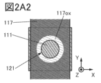
- 2A1 and 2A2 are plan views showing an example of the configuration of a semiconductor device
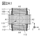
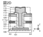
- Fig. 2B, Fig. 2C, and Fig. 2D are cross-sectional views showing an example of the configuration of a semiconductor device.
- 3A and 3B are cross-sectional and plan views illustrating an example of the configuration of a semiconductor device.
- 4A to 4C are cross-sectional views showing configuration examples of a semiconductor device.
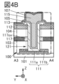
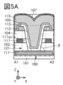
- 5A to 5D are cross-sectional views showing configuration examples of a semiconductor device.
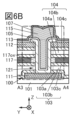
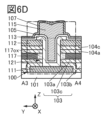
- 6A to 6D are cross-sectional views showing configuration examples of a semiconductor device.
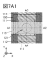
- 7A1 and 7A2 are plan views showing a configuration example of a semiconductor device, and Fig.
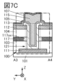
- FIG. 7B and Fig. 7C are cross-sectional views showing a configuration example of a semiconductor device.
- 8A to 8C are cross-sectional views showing configuration examples of a semiconductor device.
- 9A to 9D are cross-sectional views showing configuration examples of a semiconductor device.
- 10A and 10B are plan views showing a configuration example of a semiconductor device.
- Fig. 11A is a plan view showing a configuration example of a semiconductor device
- Fig. 11B and Fig. 11C are cross-sectional views showing the configuration example of a semiconductor device.
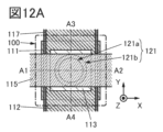
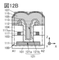
- Fig. 12A is a plan view showing a configuration example of a semiconductor device
- Fig. 12B and Fig. 12C are cross-sectional views showing the configuration example of a semiconductor device.
- FIG. 13A is a plan view illustrating an example of a method for manufacturing a semiconductor device
- FIGS. 13B and 13C are cross-sectional views illustrating the example of a method for manufacturing a semiconductor device.
- 14A is a plan view illustrating an example of a method for manufacturing a semiconductor device
- FIGS. 14B and 14C are cross-sectional views illustrating the example of a method for manufacturing a semiconductor device.
- 15A1 and 15A2 are plan views illustrating an example of a method for manufacturing a semiconductor device
- FIGS. 15B and 15C are cross-sectional views illustrating an example of a method for manufacturing a semiconductor device.
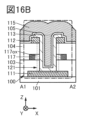
- 16A is a plan view illustrating an example of a method for manufacturing a semiconductor device, and FIGS.
- 16B and 16C are cross-sectional views illustrating the example of a method for manufacturing a semiconductor device.
- 17A to 17F are cross-sectional views illustrating an example of a method for manufacturing a semiconductor device.
- 18A1 and 18A2 are plan views illustrating an example of a method for manufacturing a semiconductor device, and FIGS. 18B and 18C are cross-sectional views illustrating an example of a method for manufacturing a semiconductor device.
- 19A1 and 19A2 are plan views illustrating an example of a method for manufacturing a semiconductor device, and FIGS. 19B and 19C are cross-sectional views illustrating an example of a method for manufacturing a semiconductor device.
- 20A1 and 20A2 are plan views illustrating an example of a method for manufacturing a semiconductor device, and FIGS.
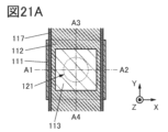
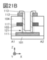
- FIGS. 21B to 21E are cross-sectional views illustrating the example of a method for manufacturing a semiconductor device.
- 21A is a plan view illustrating an example of a method for manufacturing a semiconductor device
- FIGS. 21B to 21E are cross-sectional views illustrating the example of a method for manufacturing a semiconductor device.
- Fig. 22A1 and Fig. 22A2 are plan views showing a configuration example of a memory device
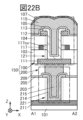
- Fig. 22B and Fig. 22C are cross-sectional views showing a configuration example of a memory device
- Fig. 22D1 and Fig. 22D2 are circuit diagrams showing a configuration example of a memory device.
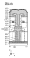
- Fig. 23A is a plan view showing a configuration example of a storage device
- FIG. 23C are cross-sectional views showing the configuration example of the storage device.
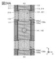
- 24A is a plan view showing a configuration example of a storage device
- FIG 24B is a cross-sectional view showing the configuration example of a storage device.
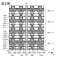
- 25A is a plan view showing a configuration example of a storage device
- FIG 25B is a cross-sectional view showing the configuration example of a storage device.
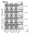
- 26A is a plan view showing a configuration example of a storage device
- FIG 26B is a cross-sectional view showing the configuration example of a storage device.
- FIG. 27 is a cross-sectional view showing a configuration example of a storage device.
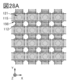
- 28A to 28C are plan views showing configuration examples of a storage device.
- FIG. 30 is a block diagram showing an example of the configuration of a storage device.
- 31A is a schematic diagram showing a configuration example of a memory device
- FIG 31B is a circuit diagram showing a configuration example of a memory device.
- 32A and 32B are schematic diagrams showing configuration examples of a storage device.
- FIG. 33 is a circuit diagram showing a configuration example of a memory device.
- 34A and 34B are diagrams showing an example of a chip on which a memory device is mounted.
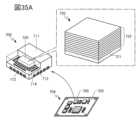
- 35A and 35B are diagrams illustrating an example of an electronic component.
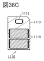
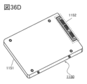
- 36A to 36E are schematic diagrams showing an example of a storage device.
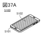
- 37A to 37H are diagrams showing an example of an electronic component.
- FIG. 30 is a block diagram showing an example of the configuration of a storage device.
- 31A is a schematic diagram showing a configuration example of a memory device
- FIG 31B is a circuit diagram showing a configuration example of a memory device.
- 32A and 32B are
- Fig. 39A is a cross-sectional view showing the structure of a sample
- Fig. 39B is a schematic diagram showing a measurement system.
- 40A to 40C are cross-sectional STEM images of the sample.
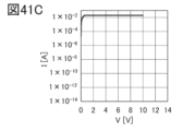
- 41A to 41C are graphs showing current-voltage characteristics.
- the position, size, range, etc. of each component shown in the drawings may not represent the actual position, size, range, etc.
- the disclosed invention is not necessarily limited to the position, size, range, etc. disclosed in the drawings.
- a layer or resist mask may be unintentionally reduced by a process such as etching, but this may not be reflected in the drawings for ease of understanding.
- ordinal numbers “first” and “second” are used for convenience and do not limit the number of components or the order of the components (e.g., the order of processes or the order of stacking).
- ordinal numbers attached to components in one place in this specification may not match the ordinal numbers attached to the same components in other places in this specification or in the claims.
- a transistor is a type of semiconductor element that can perform functions such as amplifying current or voltage and switching operations that control conduction or non-conduction.
- transistor includes an IGFET (Insulated Gate Field Effect Transistor) and a thin film transistor (TFT).
- a transistor is an element having at least three terminals including a gate, a drain, and a source.
- a transistor has a region (also called a channel formation region) where a channel is formed between the drain (drain terminal, drain region, or drain electrode) and the source (source terminal, source region, or source electrode), and a current can flow between the source and drain through the channel formation region.
- a channel formation region refers to a region through which a current mainly flows.
- source and drain may be interchanged when transistors of different polarity are used, or when the direction of current changes during circuit operation. For this reason, in this specification, the terms “source” and “drain” may be used interchangeably.
- the impurity of a semiconductor refers to, for example, anything other than the main component constituting the semiconductor.
- an element with a concentration of less than 0.1 atomic% can be said to be an impurity.
- the density of defect states in the semiconductor may increase or the crystallinity may decrease.
- examples of impurities that change the characteristics of the semiconductor include, for example, Group 1 elements, Group 2 elements, Group 13 elements, Group 14 elements, Group 15 elements, and transition metals other than the main components of the oxide semiconductor. Specific examples include, for example, hydrogen, lithium, sodium, silicon, boron, phosphorus, carbon, and nitrogen.
- water may also function as an impurity.
- oxygen vacancies also referred to as Vo
- an oxynitride refers to a material whose composition contains more oxygen than nitrogen.
- An oxynitride refers to a material whose composition contains more nitrogen than oxygen.
- SIMS secondary ion mass spectrometry
- XPS X-ray photoelectron spectroscopy
- the terms “film” and “layer” can be interchanged depending on the situation.
- the term “conductive layer” can be changed to the term “conductive film”, and the term “conductive film” can be changed to the term “conductive layer”.
- the term “insulating film” can be changed to the term “insulating layer”, and the term “insulating layer” can be changed to the term “insulating film”.
- the term “semiconductor film” can be changed to the term “semiconductor layer", and the term “semiconductor layer” can be changed to the term “semiconductor film”.
- parallel refers to a state in which two straight lines are arranged at an angle of -10 degrees or more and 10 degrees or less. Therefore, it also includes cases in which the angle is -5 degrees or more and 5 degrees or less.
- approximately parallel refers to a state in which two straight lines are arranged at an angle of -30 degrees or more and 30 degrees or less.
- Perfect refers to a state in which two straight lines are arranged at an angle of 80 degrees or more and 100 degrees or less. Therefore, it also includes cases in which the angle is 85 degrees or more and 95 degrees or less.
- approximately perpendicular refers to a state in which two straight lines are arranged at an angle of 60 degrees or more and 120 degrees or less.
- Voltage refers to the potential difference from a reference potential, and if the reference potential is the ground potential, for example, “voltage” can be interchanged with “potential.” Note that ground potential does not necessarily mean 0 V. Furthermore, potential is relative, and as the reference potential changes, for example, the potential supplied to wiring, the potential applied to a circuit, and the potential output from a circuit also change.
- electrically connected includes cases where the connection is made via "something that has some kind of electrical action.”
- something that has some kind of electrical action is not particularly limited as long as it allows the transmission and reception of electrical signals between the connected objects.
- something that has some kind of electrical action includes electrodes or wiring, as well as switching elements such as transistors, resistive elements, coils, capacitance, and other elements with various functions.
- the off-state current refers to leakage current between the source and drain when a transistor is in an off state (also referred to as a non-conducting state or a cut-off state).
- the off state refers to a state in which the voltage Vgs between the gate and source of an n-channel transistor is lower than the threshold voltage Vth (higher than Vth for a p-channel transistor).
- the top surface shape of a certain component refers to the contour shape of the component in a planar view.
- a planar view refers to a view from the normal direction of the surface on which the component is formed or the surface of the support (e.g., substrate) on which the component is formed.
- a tapered shape refers to a shape in which at least a part of the side of the structure is inclined with respect to the substrate surface or the surface to be formed.
- the side of the structure, the substrate surface, and the surface to be formed do not necessarily need to be completely flat, and may be approximately planar with a fine curvature, or approximately planar with fine irregularities.
- A covers B
- at least a part of A covers B. Therefore, for example, it can be rephrased as saying that A has an area that covers B.
- metal oxide is a metal oxide in a broad sense.
- Metal oxides are classified into oxide insulators, oxide conductors (including transparent oxide conductors), and oxide semiconductors (also referred to as oxide semiconductors or simply OS).
- oxide semiconductors also referred to as oxide semiconductors or simply OS.
- the metal oxide when a metal oxide is used in the semiconductor layer of a transistor, the metal oxide may be referred to as an oxide semiconductor.
- OS transistor when a transistor is referred to as an OS transistor, it can be rephrased as a transistor having a metal oxide or an oxide semiconductor.
- metal oxides containing nitrogen may also be collectively referred to as metal oxides. Metal oxides containing nitrogen may also be referred to as metal oxynitrides.
- the transistor can be a transistor in which a semiconductor layer is provided inside an opening formed in a first interlayer insulating layer on a substrate and a second interlayer insulating layer on the first interlayer insulating layer.
- the channel length direction of the transistor can be set along the side surfaces of the first and second interlayer insulating layers in the opening. Therefore, the channel length is no longer affected by the performance of an exposure device used to manufacture the transistor, and the channel length can be made smaller than the limit resolution of the exposure device. Therefore, the on-current of the transistor can be increased, and the semiconductor device can be operated at high speed.
- a first conductive layer provided under the opening is used as one of the source electrode or drain electrode of the transistor.
- first and second interlayer insulating layers are provided on the first conductive layer, and openings are provided in the first and second interlayer insulating layers so as to reach the first conductive layer.
- a second conductive layer provided on the second interlayer insulating layer and having an opening overlapping the above opening is used as the other of the source electrode or drain electrode of the transistor.
- a semiconductor layer is provided so as to have a region in contact with the first conductive layer and a region in contact with the second conductive layer.
- a first gate insulating layer is provided on the semiconductor layer, and a first gate electrode is provided on the first gate insulating layer.
- the threshold voltage of the transistor when the channel length of the transistor is reduced, the threshold voltage of the transistor is reduced and, for example, the transistor may have normally-on characteristics. Therefore, a second gate electrode is provided in the transistor included in the semiconductor device of one embodiment of the present invention. This makes it possible to control, for example, the threshold voltage of the transistor. Therefore, for example, the threshold voltage of the transistor can be made higher than when the second gate electrode is not provided in the transistor, and the transistor can be prevented from having normally-on characteristics. In other words, the transistor can have normally-off characteristics. This makes it possible to provide a semiconductor device with good electrical characteristics.
- a transistor having normally-on characteristics means that a channel exists in the semiconductor layer and a current flows between the source and drain of the transistor even when a potential is not supplied to the gate of the transistor.
- a transistor having normally-off characteristics means that no current flows between the source and drain of the transistor when a potential is not supplied to the gate of the transistor.
- a transistor having normally-on characteristics means that a current flows between the source and drain of the transistor even when a potential is not supplied to the first gate electrode, which has a function of controlling the magnitude of the current flowing in the channel formation region of the semiconductor layer.
- a transistor having normally-off characteristics means that no current flows between the source and drain of the transistor when a potential is not supplied to the first gate electrode.
- the second gate electrode is provided between the first interlayer insulating layer and the second interlayer insulating layer.
- the second gate electrode has an opening that overlaps with the openings provided in the first and second interlayer insulating layers, and the side surface of the opening and the region in the vicinity thereof are oxide regions.
- the oxide region is a region having a higher electrical resistivity than the region other than the oxide region of the second gate electrode, and has insulating properties.
- the oxide region covers the region of the semiconductor layer that is located inside the opening of the second gate electrode. As described above, the oxide region of the second gate electrode functions as a second gate insulating layer.
- a transistor included in a semiconductor device first, a first conductive layer on a substrate, a first interlayer insulating layer on the first conductive layer, a second gate electrode on the first interlayer insulating layer, a second interlayer insulating layer on the second gate electrode, and a second conductive layer on the second interlayer insulating layer are formed in this order.
- an opening reaching the first conductive layer is formed in the first interlayer insulating layer, the second gate electrode, the second interlayer insulating layer, and the second conductive layer.
- an oxidation treatment is performed on the side surface of the second gate electrode in the opening.
- the oxidation treatment may be a microwave treatment in an atmosphere containing oxygen.
- An oxide region is formed in the second gate electrode by the oxidation treatment, and the oxide region functions as the second gate insulating layer.
- microwave processing refers to processing using a device having a power source that generates high-density plasma using microwaves.
- microwaves refer to electromagnetic waves having a frequency of 300 MHz or more and 300 GHz or less.
- Microwave processing can also be called microwave-excited high-density plasma processing.
- a semiconductor layer, a first gate insulating layer, and a first gate electrode are formed in this order so as to have a region located inside the opening.
- a transistor included in a semiconductor device according to one embodiment of the present invention can be manufactured.
- FIG 1 is a perspective view showing a configuration example of a semiconductor device according to one embodiment of the present invention, and shows a configuration example of a transistor 100 included in the semiconductor device.
- FIG 2A1 is a plan view showing the configuration example when FIG 1 is viewed in the Z direction, specifically, for example, from the top in the Z direction. In FIG 2A1, some elements such as an insulating layer are omitted for clarity of the drawing. Some elements are also omitted in the plan views shown later.
- FIG 2B is a cross-sectional view taken along dashed line A1-A2 in FIG 2A1
- FIG 2C is a cross-sectional view taken along dashed line A3-A4 in FIG 2A1.
- the X direction, the Y direction, and the Z direction are shown on the coordinate axes.
- the direction of the dashed line A1-A2 is the X direction
- the direction of the dashed line A3-A4 is the Y direction
- the direction perpendicular to the XY plane is the Z direction.
- the X direction, the Y direction, and the Z direction can be mutually intersecting directions, specifically, mutually perpendicular directions.
- the definitions of the X direction, the Y direction, and the Z direction are shown on the coordinate axes, but the definitions may be the same as those in 1, 2A1, 2B, and 2C, or may be different.
- the X direction, the Y direction, and the Z direction are shown by arrows, but the forward direction and the reverse direction are not distinguished unless otherwise specified. The same applies to the following drawings.
- one of the X direction, Y direction, and Z direction may be referred to as the "first direction.”
- the other may be referred to as the “second direction.”
- the remaining may be referred to as the "third direction.”
- the semiconductor device of one embodiment of the present invention has an insulating layer 101 on a substrate (not shown) and a transistor 100 on the insulating layer 101.
- the semiconductor device of one embodiment of the present invention also has an insulating layer 103 on the insulating layer 101, an insulating layer 104 on the insulating layer 103, and an insulating layer 107 on the insulating layer 104 and on the transistor 100.
- the insulating layer 101, the insulating layer 103, and the insulating layer 104 function as interlayer insulating layers.
- the layers that function as interlayer insulating layers, including these insulating layers, are preferably planarized. Note that the layers that function as interlayer insulating layers do not have to be planarized.
- the transistor 100 has a conductive layer 111, a conductive layer 112, a semiconductor layer 113, an insulating layer 105, a conductive layer 115, and a conductive layer 117.
- FIG. 2A2 shows a plan view in which the conductive layer 115, the semiconductor layer 113, and the conductive layer 112 are omitted from FIG. 2A1.
- FIG. 2A1 shows an example in which the conductive layer 115 is provided to extend in the X direction, and the conductive layer 112 is provided to extend in the Y direction.
- FIGS. 2A1 and 2A2 show an example in which the conductive layer 117 is provided to extend in the Y direction.
- the insulating layers 101, 103, 104, 105, and 107 can be made of an insulator described in the section [Insulator] below, in a single layer or a stacked layer.
- the conductive layers 111, 112, 115, and 117 can be made of a conductor described in the section [Conductor] below, in a single layer or a stacked layer.
- the semiconductor layer 113 can be made of a metal oxide described in the section [Metal oxide] below, in a single layer or a stacked layer.
- the semiconductor layer 113 can be made of a material such as silicon described in the section [Other semiconductor materials] below, in a single layer or a stacked layer.
- a transistor using metal oxide for the channel formation region of the semiconductor layer is called an OS transistor.
- a transistor using silicon for the channel formation region of the semiconductor layer is called a Si transistor.
- the transistor 100 can be an OS transistor.
- the transistor 100 can be a Si transistor.
- the conductive layer 111 functions as one of the source electrode and drain electrode of the transistor 100.
- the conductive layer 112 functions as the other of the source electrode and drain electrode of the transistor 100.
- the insulating layer 105 functions as a gate insulating layer of the transistor 100.
- the conductive layer 115 and the conductive layer 117 function as gate electrodes of the transistor 100.
- a conductive layer 111 is provided on the insulating layer 101, an insulating layer 103 is provided on the insulating layer 101 and on the conductive layer 111, a conductive layer 117 is provided on the insulating layer 103, an insulating layer 104 is provided on the insulating layer 103 and on the conductive layer 117, and a conductive layer 112 is provided on the insulating layer 104.
- the conductive layer 111 and the conductive layer 117 can have a region where they overlap with each other through the insulating layer 103.
- the conductive layer 117 and the conductive layer 112 can have a region where they overlap with each other through the insulating layer 104.
- the conductive layer 111 and the conductive layer 112 can have a region where they overlap with each other through the insulating layer 103 and the insulating layer 104.
- the insulating layer 103, the conductive layer 117, the insulating layer 104, and the conductive layer 112 have an opening 121 that reaches the conductive layer 111.
- the opening 121 can be formed by processing a part of the insulating layer 103, the conductive layer 117, the insulating layer 104, and the conductive layer 112, for example, by an etching method, after the layers are formed. In particular, processing by a dry etching method is preferable because it is suitable for fine processing.
- 2A1 and 2A2 show an example in which the shape of the opening 121 is circular in a plan view.
- the processing accuracy when forming the opening 121 can be improved, and the opening 121 can be formed with a fine size.
- a circle is not limited to a perfect circle.
- the planar shape of the opening 121 may be, for example, an ellipse.
- 1, 2A1, and 2B show an example in which, in the X direction, the side end of conductive layer 111 is located outside the side end of conductive layer 117 that does not face opening 121, and the side end of conductive layer 117 that does not face opening 121 is located outside the side end of conductive layer 112 that does not face opening 121. That is, in the X direction, Fig.
- 1, 2A1, and 2B show an example in which the side end of conductive layer 112 that does not face opening 121 overlaps conductive layer 117 and conductive layer 111, and the side end of conductive layer 117 that does not face opening 121 overlaps conductive layer 111, but the side end of conductive layer 111 does not overlap conductive layer 112 and conductive layer 117, and the side end of conductive layer 117 that does not face opening 121 does not overlap conductive layer 112.
- the side end of the conductive layer 111 may be located inside the side end of the conductive layer 117 that does not face the opening 121, or may be located inside the side end of the conductive layer 112 that does not face the opening 121.
- the side end of the conductive layer 117 may be located inside the side end of the conductive layer 112 that does not face the opening 121.
- the semiconductor layer 113 is provided to cover the opening 121 and to have a region located inside the opening 121.
- the semiconductor layer 113 can have a shape that follows the shapes of the upper surface of the conductive layer 111, the side surface of the insulating layer 103, the side surface of the insulating layer 104, and the side and upper surface of the conductive layer 112. As a result, the semiconductor layer 113 has a recess at a position that overlaps with the opening 121.
- the semiconductor layer 113 can have a region in contact with the upper surface of the conductive layer 111, a region in contact with the side surface of the insulating layer 103, a region in contact with the side surface of the insulating layer 104, a region in contact with the side surface of the conductive layer 112, and a region in contact with the upper surface of the conductive layer 112.
- the semiconductor layer 113 preferably covers the side end of the conductive layer 112 on the opening 121 side.
- Figures 1, 2A1, 2B, and 2C show a configuration in which the side end of the semiconductor layer 113 is located on the conductive layer 112. This configuration can also be said to be such that the lower end of the semiconductor layer 113 contacts the upper surface of the conductive layer 112.
- the side end of the semiconductor layer 113 may be located outside the side end of the conductive layer 112. In this case, the semiconductor layer 113 can cover the side of the conductive layer 112 that does not face the opening 121.
- the upper end refers to the uppermost part of the side end
- the lower end refers to the lowermost part of the side end.
- the upper end and the lower end are each part of the side end.
- Fig. 1, Fig. 2A1, Fig. 2B, and Fig. 2C show an example in which the semiconductor layer 113 is divided in both the X direction and the Y direction to form islands.
- “island-like” refers to a state in which two or more layers made of the same material and formed in the same process are physically separated.
- the insulating layer 105 is provided so as to cover the opening 121 and have a region located inside the opening 121.
- the insulating layer 105 is provided on the semiconductor layer 113, the conductive layer 112, and the insulating layer 104.
- the insulating layer 105 can have a shape that follows the shapes of the upper surface and side surface of the semiconductor layer 113, the upper surface and side surface of the conductive layer 112, and the upper surface of the insulating layer 104. Since the insulating layer 105 has a shape that follows the upper surface and side surface of the semiconductor layer 113, the insulating layer 105 has a recess at a position overlapping the opening 121.
- the insulating layer 105 can have a region in contact with the upper surface of the semiconductor layer 113, a region in contact with the side surface of the semiconductor layer 113, a region in contact with the upper surface of the conductive layer 112, a region in contact with the side surface of the conductive layer 112, and a region in contact with the upper surface of the insulating layer 104.
- the conductive layer 115 is provided on the insulating layer 105 and can have a region in contact with the upper surface of the insulating layer 105 and the side surface of the recess.
- the conductive layer 115 has a region located inside the opening 121.
- the conductive layer 115 and the semiconductor layer 113 have regions that face each other across the insulating layer 105 at positions along the sidewalls and bottom of the opening 121.
- the semiconductor layer 113 can be configured to cover the side surface and bottom surface of the conductive layer 115 through the insulating layer 105 inside the opening 121.
- the insulating layer 105 can have a region in contact with the side surface of the semiconductor layer 113, a region in contact with the upper surface of the recess of the semiconductor layer 113, a region in contact with the side surface of the conductive layer 115, and a region in contact with the bottom surface of the conductive layer 115.
- the transistor 100 shown in FIG. 1, FIG. 2B, and FIG. 2C is a transistor in which a semiconductor layer, a gate insulating layer, and a gate electrode are provided inside an opening formed in an interlayer insulating layer.
- the channel length direction of the transistor 100 can be set to a direction along the side surfaces of the insulating layers 103 and 104 in the opening 121. Therefore, the channel length is not affected by the performance of the exposure device used to manufacture the transistor 100, so that the channel length can be made smaller than the limit resolution of the exposure device. Therefore, the on-current of the transistor 100 can be increased. As a result, a semiconductor device that operates at high speed can be provided. Note that, for example, FIG.
- 2A1 shows an example in which the entire opening 121 has a region overlapping with the conductive layer 111, the semiconductor layer 113, and the conductive layer 115, but a part of the opening 121 does not have to overlap with at least one of the conductive layer 111, the semiconductor layer 113, and the conductive layer 115.
- a portion of the conductive layer 115 is located outside the opening 121, i.e., on the conductive layer 112 and the insulating layer 104.
- the side end of the conductive layer 115 is located inside the side end of the semiconductor layer 113. This makes it possible to reduce the parasitic capacitance formed by, for example, the conductive layer 112, the insulating layer 105, and the conductive layer 115.
- the side end of the conductive layer 115 may be located outside the side end of the semiconductor layer 113. In this case, the conductive layer 115 can cover the entire semiconductor layer 113.
- a conductive layer 117 having an opening 121 is provided between the insulating layer 103 and the insulating layer 104.
- the insulating layer 104 can cover the upper surface and side surface of the conductive layer 117.
- the side surface of the conductive layer 117 at the opening 121 and the region in the vicinity thereof are oxide regions 117ox.
- the oxide region 117ox is a region having a higher electrical resistivity than the conductive layer 117 and has insulating properties.
- the oxide region 117ox since the oxide region 117ox has insulating properties, the oxide region 117ox can be a region having a higher electrical resistivity than the semiconductor layer 113.
- the oxide region 117ox covers a region of the semiconductor layer 113 located inside the opening 121. Specifically, the oxide region 117ox covers a region of the semiconductor layer 113 located inside the opening 121 provided in the conductive layer 117. For example, in the opening 121, the oxide region 117ox is in contact with the semiconductor layer 113. Furthermore, the non-oxidized region of the conductive layer 117 covers the oxide region 117ox. For example, the non-oxidized region of the conductive layer 117 is not in contact with the semiconductor layer 113. As described above, the conductive layer 117 functions as a gate electrode, and the oxide region 117ox functions as a gate insulating layer. Note that the oxide region 117ox does not need to be oxidized as long as it has insulating properties. The oxide region 117ox can be referred to as a high resistance region.
- the oxide region 117ox is included in the conductive layer 117, that is, the oxide region 117ox can be part of the conductive layer 117. Note that the oxide region 117ox does not necessarily have to be included in the conductive layer 117.
- the transistor 100 is a transistor with a dual gate structure having two gate electrodes, and the conductive layer 115 functioning as the first gate electrode and the conductive layer 117 functioning as the second gate electrode are provided so as to have a region sandwiching the channel formation region of the semiconductor layer 113 inside the opening 121.
- the magnitude of the current flowing through the channel formation region of the semiconductor layer 113 can be controlled based on the potential of the conductive layer 115, and the threshold voltage of the transistor 100 can be controlled based on the potential of the conductive layer 117.
- the channel length of the transistor 100 is small, for example, smaller than the limit resolution of an exposure device.
- the threshold voltage of the transistor 100 is small, and for example, the transistor 100 may have normally-on characteristics. Therefore, the threshold voltage of the transistor 100 is controlled by controlling the potential of the conductive layer 117, specifically, for example, the threshold voltage of the transistor 100 is made higher than when the conductive layer 117 is not provided in the transistor 100, thereby preventing the transistor 100 from having normally-on characteristics. In other words, the transistor 100 can have normally-off characteristics. Note that by controlling the threshold voltage of the transistor 100, the threshold voltage of the transistor 100 can be made smaller to increase the on-current of the transistor 100.
- the variation in electrical characteristics for each transistor 100 can be reduced.
- a semiconductor device with good electrical characteristics can be provided.
- transistor 100 is a p-channel transistor
- one embodiment of the present invention can be applied by appropriately reversing the magnitude relationships of the various potentials and threshold voltages shown in this specification from the case where the transistor 100 is an n-channel transistor.
- the first gate electrode can be referred to as a front gate electrode
- the second gate electrode can be referred to as a back gate electrode
- the insulating layer 105 can be the first gate insulating layer
- the oxide region 117ox can be the second gate insulating layer.
- the first gate electrode and the second gate electrode may be interchanged.
- the conductive layer 115 may be used as the second gate electrode
- the conductive layer 117 may be used as the first gate electrode.
- the insulating layer 105 can be referred to as the second gate insulating layer
- the insulating layer 106 can be referred to as the first gate insulating layer.
- the conductive layer 117 can be supplied with, for example, a constant potential. For example, supplying a ground potential or a negative potential to the conductive layer 117 can prevent the transistor 100 from becoming normally on. Note that the same potential as the potential of the conductive layer 115 may be supplied to the conductive layer 117. This can increase, for example, the on-current of the transistor 100.
- the transistor 100 is an n-channel transistor, for example, the potential supplied to the conductive layer 117 when the transistor 100 is turned on may be higher than the potential supplied to the conductive layer 117 when the transistor 100 is turned off. For example, a positive potential may be supplied to the conductive layer 117 when the transistor 100 is turned on, and a ground potential or a negative potential may be supplied to the conductive layer 117 when the transistor 100 is turned off.
- the conductive layer 117 is made of a material whose electrical resistivity increases due to a chemical reaction such as oxidation, and which becomes insulating, for example.
- a metal or a metal nitride can be used as the conductive layer 117.
- materials that can be used for the conductive layer 117 include tantalum nitride, titanium nitride, nitrides containing titanium and aluminum, nitrides containing tantalum and aluminum, and tungsten.
- the oxide region 117ox contains an oxide of the material contained in the conductive layer 117.
- the oxide region 117ox contains tantalum oxide
- titanium nitride is used as the conductive layer 117
- the oxide region 117ox contains titanium oxide.
- the oxide region 117ox may contain, for example, nitrogen.
- the electric field from the conductive layer 117 may not reach the region of the semiconductor layer 113 that is not covered by the conductive layer 117. If the electrical resistivity of the region of the semiconductor layer 113 that is not reached by the electric field from the conductive layer 117 is lower than the electrical resistivity of the region that is reached by the electric field from the conductive layer 117, this is preferable, for example, because the on-current of the transistor 100 can be increased.
- the electrical resistivity of the region in contact with the insulating layer 103 and the region in contact with the insulating layer 104 is preferably lower than the electrical resistivity of the region in contact with the oxide region 117ox.
- an insulator containing nitrogen when used for the insulating layer 103 and the insulating layer 104, nitrogen can be supplied to the semiconductor layer 113.
- a metal oxide when used for the semiconductor layer 113, electrons that are carriers are generated in the semiconductor layer 113, and the carrier concentration may increase. Therefore, for example, the electrical resistivity of the region in contact with the insulating layer 103 and the region in contact with the insulating layer 104 can be made lower than the electrical resistivity of the region in contact with the oxide region 117ox.
- An example of an insulator containing nitrogen is silicon nitride. Also, for example, silicon nitride oxide or aluminum nitride may be used for the insulating layer 103 and the insulating layer 104.
- an insulator containing oxygen may be used as the insulating layer 103 and the insulating layer 104.
- the insulating layer 103 and the insulating layer 104 disposed near the channel formation region of the semiconductor layer 113 contain oxygen that is desorbed by heating (hereinafter, sometimes referred to as excess oxygen).
- excess oxygen oxygen that is desorbed by heating
- insulators containing oxygen include silicon oxide and silicon oxynitride.
- an insulator having a function of capturing hydrogen or a function of fixing hydrogen may be used as the insulating layer 103 and the insulating layer 104 disposed near the channel formation region of the semiconductor layer 113.
- hydrogen in the channel formation region of the semiconductor layer 113 can be captured or fixed (also called gettering), and the hydrogen concentration in the semiconductor layer 113 can be reduced.
- insulating layers 103 and 104 include magnesium oxide and aluminum oxide.
- the oxide region 117ox of the conductive layer 117 can be formed by forming an opening 121 in the conductive layer 112, the insulating layer 104, the conductive layer 117, and the insulating layer 103, and then performing an oxidation treatment.
- an oxidation treatment for example, a microwave treatment in an atmosphere containing oxygen can be mentioned.
- the oxidation treatment is performed not only on the conductive layer 117 but also on the conductive layer 111 and the conductive layer 112. Therefore, a material that is less likely to be oxidized than the conductive layer 117 or a material that has conductivity even when oxidized is used for the conductive layer 111 and the conductive layer 112.
- a conductive material containing oxygen can be used for the conductive layer 111 and the conductive layer 112.
- indium tin oxide also referred to as ITO
- indium tin oxide with silicon added also referred to as ITSO
- indium zinc oxide also referred to as IZO (registered trademark)
- ITO indium tin oxide
- ITSO indium tin oxide with silicon added
- IZO indium zinc oxide
- the like can be used as a single layer or a stacked layer for the conductive layer 111 and the conductive layer 112.
- An insulating layer 107 is provided on the conductive layer 115 and on the insulating layer 105.
- the insulating layer 107 can be provided so as to cover the top and side surfaces of the conductive layer 115.
- the insulating layer 107 has a function of preventing impurities from entering the transistor 100, for example, preventing impurities from entering the semiconductor layer 113.
- FIG. 1D shows an example in which the side end of the insulating layer 105 shown in FIG. 2C coincides or roughly coincides with the side end of the conductive layer 115.
- FIG. 2D shows an example in which the side end of the insulating layer 105 shown in FIG. 2C coincides or roughly coincides with the side end of the conductive layer 115.
- FIG. 3A is an enlarged view of the transistor 100 shown in FIG. 2C and its vicinity.
- FIG. 3B is a plan view of the XY plane of the transistor 100 shown in FIG. 3A. Note that the conductive layer 111 and the conductive layer 117 are not shown in FIG. 3B.
- the semiconductor layer 113 has a region 113i and regions 113na and 113nb arranged to sandwich the region 113i.
- Region 113na is a region in contact with conductive layer 111 of semiconductor layer 113. At least a portion of region 113na functions as one of the source region or drain region of transistor 100.
- Region 113nb is a region in contact with conductive layer 112 of semiconductor layer 113. At least a portion of region 113nb functions as the other of the source region or drain region of transistor 100.
- conductive layer 112 is in contact with the entire outer periphery of semiconductor layer 113. Therefore, the other of the source region or drain region of transistor 100 can be formed on the entire outer periphery of a portion of semiconductor layer 113 formed in the same layer as conductive layer 112.
- Region 113i is a region between regions 113na and 113nb of the semiconductor layer 113. At least a part of region 113i functions as a channel formation region of the transistor 100. That is, the channel formation region of the transistor 100 is located in a region of the semiconductor layer 113 between the conductive layer 111 and the conductive layer 112. It is also said that the channel formation region of the transistor 100 is located in a region of the semiconductor layer 113 that is in contact with the insulating layer 103 or in the vicinity thereof, in contact with the oxide region 117ox or in the vicinity thereof, and in contact with the insulating layer 104 or in the vicinity thereof.
- the channel length of a transistor is the distance between the source region and the drain region. In other words, it can be said that the channel length of the transistor 100 is determined by the thickness of the insulating layer 103, the oxide region 117ox, and the insulating layer 104 on the conductive layer 111.
- the channel length L of the transistor 100 is indicated by a dashed double-headed arrow. In a cross-sectional view, the channel length L is the distance between the end of the region where the semiconductor layer 113 and the conductive layer 111 contact each other and the end of the region where the semiconductor layer 113 and the conductive layer 112 contact each other. In other words, the channel length L corresponds to the length of the side of the insulating layer 103, the oxide region 117ox, and the insulating layer 104 at the opening 121 in a cross-sectional view.
- the channel length is set by the exposure limit of photolithography, but in the present invention, the channel length can be set by the film thickness of the insulating layer 103, the oxide region 117ox, and the insulating layer 104 in the region where they overlap with the conductive layer 111. Therefore, the channel length of the transistor 100 can be made to be a very fine structure (for example, 60 nm or less, 50 nm or less, 40 nm or less, 30 nm or less, 20 nm or less, or 10 nm or less, and 1 nm or more, or 5 nm or more) that is below the exposure limit of photolithography. This increases the on-current of the transistor 100. Therefore, a semiconductor device that operates at high speed can be provided.
- the transistor 100 having the structure shown in FIG. 3A and FIG. 3B can have a shorter channel length than, for example, a planar transistor.
- a metal oxide for the semiconductor layer 113.
- the semiconductor layer 113 may be made of a material other than a metal oxide, such as silicon.
- the channel formation region, source region, and drain region can be formed in the opening 121. This allows the area occupied by the transistor to be reduced compared to, for example, a planar type transistor in which the channel formation region, source region, and drain region are provided separately on the XY plane. This allows the semiconductor device to be miniaturized.
- the channel width of the transistor 100 is determined by the length of the outer periphery of the semiconductor layer 113. That is, it can be said that the channel width of the transistor 100 is determined by the size of the maximum width of the opening 121 (maximum diameter when the opening 121 is circular in a plan view).
- the maximum width D of the opening 121 is indicated by a double-headed arrow of a two-dot chain line.
- the channel width W of the transistor 100 is indicated by a double-headed arrow of a one-dot chain line.
- the maximum width D of the opening 121 is, for example, 5 nm or more, 10 nm or more, or 20 nm or more, and is preferably 100 nm or less, 60 nm or less, 50 nm or less, 40 nm or less, or 30 nm or less.
- the maximum width D of the opening 121 corresponds to the diameter of the opening 121, and the channel width W can be calculated as "D x ⁇ ".
- the channel length L of the transistor 100 is preferably at least smaller than the channel width W of the transistor 100.
- the channel length L of the transistor 100 is 0.1 to 0.99 times, preferably 0.5 to 0.8 times, the channel width W of the transistor 100.
- the semiconductor layer 113 the insulating layer 105, and the conductive layer 115 in a concentric manner, the distance between the conductive layer 115 and the semiconductor layer 113 becomes approximately uniform. Therefore, a gate electric field can be applied approximately uniformly to the semiconductor layer 113.
- the sidewalls of the opening 121 are preferably perpendicular to the top surface of the conductive layer 111, for example. With such a configuration, the transistor 100 can be miniaturized. Note that the sidewalls of the opening 121 may be tapered.
- the semiconductor layer 113 can be made of a metal oxide described in the section [Metal oxide] below, in a single layer or a multilayer structure.
- the semiconductor layer 113 can be made of a material such as silicon described in the section [Other semiconductor materials] below, in a single layer or a multilayer structure.
- the composition in the vicinity includes a range of ⁇ 30% of the desired atomic ratio.
- the above atomic ratio is not limited to the atomic ratio of the formed metal oxide film, but may be the atomic ratio of the sputtering target used to form the metal oxide film.
- energy dispersive X-ray spectrometry EDX
- XPS XPS
- ICP-MS inductively coupled plasma mass spectrometry
- ICP-AES inductively coupled plasma-atomic emission spectrometry
- the analysis may be performed by combining a plurality of these techniques. Note that for elements with low content, the actual content may differ from the content obtained by analysis due to the influence of analytical accuracy. For example, if the content of element M is low, the content of element M obtained by analysis may be lower than the actual content.
- the atomic layer deposition (ALD) method can be suitably used to form metal oxides.
- the metal oxide may be formed by sputtering or chemical vapor deposition (CVD).
- the composition of the formed metal oxide may differ from the composition of the sputtering target.
- the zinc content in the formed metal oxide may decrease to about 50% compared to the sputtering target.
- the metal oxide used for the semiconductor layer 113 is preferably crystalline.
- crystalline oxide semiconductors include CAAC-OS (c-axis aligned crystalline oxide semiconductor), nc-OS (nanocrystalline oxide semiconductor), polycrystalline oxide semiconductor, and single crystal oxide semiconductor. It is preferable to use CAAC-OS or nc-OS as the semiconductor layer 113, and it is particularly preferable to use CAAC-OS.
- CAAC-OS preferably has multiple layered crystal regions with the c-axis oriented in the normal direction to the surface on which it is formed.
- the semiconductor layer 113 preferably has layered crystals that are approximately parallel to the sidewall of the opening 121, particularly the side surfaces of the insulating layer 103, the oxide region 117ox, and the insulating layer 104. With this configuration, the layered crystals of the semiconductor layer 113 are formed approximately parallel to the channel length direction of the transistor 100, thereby increasing the on-current of the transistor 100.
- CAAC-OS is a metal oxide that has a highly crystalline and dense structure and has few impurities and defects (e.g., oxygen vacancies, etc.).
- a temperature e.g. 400° C. or higher and 600° C. or lower
- the CAAC-OS can be made to have a more crystalline and dense structure. In this way, the density of the CAAC-OS can be further increased, thereby further reducing the diffusion of impurities or oxygen in the CAAC-OS.
- the semiconductor layer 113 by using a crystalline metal oxide such as CAAC-OS as the semiconductor layer 113, it is possible to suppress the extraction of oxygen from the semiconductor layer 113 by the source electrode or drain electrode. As a result, even when heat treatment is performed, oxygen can be suppressed from being extracted from the semiconductor layer 113, so that the transistor 100 is stable against high temperatures (so-called thermal budget) in the manufacturing process.
- a crystalline metal oxide such as CAAC-OS
- the crystallinity of the semiconductor layer 113 can be analyzed, for example, by X-ray diffraction (XRD), a transmission electron microscope (TEM), or electron diffraction (ED). Alternatively, the analysis may be performed by combining a plurality of these techniques.
- XRD X-ray diffraction
- TEM transmission electron microscope
- ED electron diffraction
- the thickness of the semiconductor layer 113 is preferably 1 nm or more, 3 nm or more, or 5 nm or more, and 20 nm or less, 15 nm or less, 12 nm or less, or 10 nm or less.
- the semiconductor layer 113 may have a stacked structure of multiple oxide layers with different chemical compositions. For example, a structure in which multiple types selected from the above metal oxides are appropriately stacked may be used.
- the semiconductor layer 113 can have a region in contact with the conductive layer 111 and a region in contact with the conductive layer 112.
- a metal compound or oxygen deficiency may be formed, and the region 113na of the semiconductor layer 113 may have a low resistance.
- the contact resistance between the semiconductor layer 113 and the conductive layer 111 can be reduced.
- the region 113nb of the semiconductor layer 113 may have a low resistance. Therefore, the contact resistance between the semiconductor layer 113 and the conductive layer 112 can be reduced.
- silicon oxide or silicon oxynitride can be used as the insulating layer 105 that functions as a gate insulating layer. Silicon oxide and silicon oxynitride are preferred because they are stable to heat.
- the insulating layer 105 may be made of a material with a high relative dielectric constant, so-called high-k material, as described in the [Insulator] section below.
- high-k material a material with a high relative dielectric constant
- hafnium oxide or aluminum oxide may be used.
- the thickness of the insulating layer 105 is preferably 0.5 nm to 15 nm, more preferably 0.5 nm to 12 nm, and even more preferably 0.5 nm to 10 nm. It is preferable that at least a portion of the insulating layer 105 has a region with the above-mentioned thickness.
- the concentration of impurities such as water and hydrogen in the insulating layer 105 is reduced. This can prevent impurities such as water and hydrogen from entering the channel formation region of the semiconductor layer 113.
- the insulating layer 105 is shown as a single layer in FIG. 1, FIG. 2B, FIG. 2C, and the like, one embodiment of the present invention is not limited to this.
- the insulating layer 105 may have a stacked structure.
- the conductive layer 115 that functions as a gate electrode can be made of a conductive material with high conductivity, such as tungsten, aluminum, or copper.
- an alloy can be used for the conductive layer 115, such as an alloy of aluminum and titanium (Al-Ti).
- the conductive layer 115 it is preferable to use a conductive material that is difficult to oxidize, or a conductive material that has a function of suppressing the diffusion of oxygen, as the conductive layer 115.
- the conductive material include a conductive material containing nitrogen (e.g., titanium nitride or tantalum nitride), and a conductive material containing oxygen (e.g., ruthenium oxide). This can suppress a decrease in the conductivity of the conductive layer 115.
- a semiconductor with high electrical conductivity, typified by polycrystalline silicon containing an impurity element such as phosphorus, or a silicide such as nickel silicide may be used as the conductive layer 115.
- the conductive layer 115 is shown as a single layer in FIG. 1, FIG. 2B, FIG. 2C, and the like, one embodiment of the present invention is not limited to this.
- the conductive layer 115 may have a stacked structure.
- the insulating layer 101 preferably has a low dielectric constant. This reduces the parasitic capacitance that occurs between wiring lines.
- a single layer or a multilayer of an insulator containing a material with a low dielectric constant, as described in the [Insulator] section below, can be used.
- silicon oxide and silicon oxynitride are preferable because they are thermally stable.
- the concentration of impurities such as water and hydrogen in the insulating layer 101 is reduced. This can prevent impurities such as water and hydrogen from entering the channel formation region of the semiconductor layer 113.
- the insulating layer 107 it is preferable to use an insulator having barrier properties against hydrogen, as described in the [Insulator] section below. This can prevent hydrogen from diffusing from the outside of the transistor 100 to the semiconductor layer 113 through the insulating layer 105.
- Silicon nitride and silicon nitride oxide each have the characteristics of releasing little impurities such as water and hydrogen from themselves, and being difficult for oxygen and hydrogen to permeate, and therefore can be suitably used for the insulating layer 107.
- an insulator having a function of capturing hydrogen or a function of fixing hydrogen as described in the section [Insulator] below, as the insulating layer 107.
- an insulator having a function of capturing hydrogen or a function of fixing hydrogen as described in the section [Insulator] below.
- Magnesium oxide, aluminum oxide, hafnium oxide, or the like can be used as the insulating layer 107.
- a stacked film of aluminum oxide and silicon nitride on the aluminum oxide may be used as the insulating layer 107.
- the configuration in which the insulating layer 107 is formed on the top surface of the transistor 100 is shown, but the present invention is not limited to this.
- the insulating layer 107 or an insulating layer having the same function and material as the insulating layer 107 may be formed on the side and bottom surfaces of the transistor 100, and the transistor 100 may be surrounded by the insulating layer 107. With this configuration, impurities such as water and hydrogen can be prevented from entering the inside of the transistor 100.
- FIG. 4A and 4B are diagrams showing a two-layer structure of the conductive layer 111 shown in FIG. 2B and FIG. 2C, respectively, which is a two-layer stack of a conductive layer 111a and a conductive layer 111b on the conductive layer 111a.
- Fig. 4C is an enlarged view of the conductive layer 111 shown in Fig. 4B and a region in the vicinity thereof.
- Fig. 4C shows a region 113na at least a part of which functions as one of the source region and the drain region of the transistor 100, and a region 113i at least a part of which functions as a channel formation region of the transistor 100.
- the opening 121 is also provided in the conductive layer 111b and reaches the conductive layer 111a.
- the semiconductor layer 113 can have a region inside the opening 121 that contacts the top surface of the conductive layer 111a and a region that contacts the side surface of the conductive layer 111b.
- the insulating layer 101, the conductive layer 111a, the conductive layer 111b, the insulating layer 103, the conductive layer 117, the insulating layer 104, and the conductive layer 112 are formed, and then an opening 121 reaching the conductive layer 111b is formed in the conductive layer 112, the insulating layer 104, the conductive layer 117, and the insulating layer 103.
- the conductive layer 117 is subjected to oxidation treatment to form an oxide region 117ox. Then, the region of the conductive layer 111b overlapping with the opening 121 is removed so that the opening 121 reaches the conductive layer 111a.
- the semiconductor layer 113, the insulating layer 105, and the conductive layer 115 are formed so as to have a region located inside the opening 121.
- the transistor 100 having the structure shown in FIG. 4A to 4C can be manufactured.
- the conductive layer 111a may be provided with a recess having a region overlapping with the opening 121.
- the opening 121 may not reach the conductive layer 111a, and a recess having an area that overlaps with the opening 121 may be provided in the conductive layer 111b.
- a part of the conductive layer 111b is removed after the oxidation treatment.
- the electrical resistance at the contact interface between the conductive layer 111 and the semiconductor layer 113 can be reduced.
- the transistor 100 when the transistor 100 is in an on state, it is possible to suppress the current from flowing between the conductive layer 111 and the conductive layer 112 of the semiconductor layer 113 and the current flowing therebetween from being reduced. Therefore, a highly reliable semiconductor device can be provided.
- a material having low oxidation resistance but high conductivity can be used for the conductive layer 111, and the range of material selection for the conductive layer 111 can be expanded. Note that, even when the conductive layer 111 is, for example, a single layer as shown in FIG. 1, FIG. 2B, FIG. 2C, etc., at least a part of the oxidized region of the conductive layer 111 may be removed after the oxidation treatment. In this case, the conductive layer 111 has a recess having an area that overlaps with the opening 121.
- the top surface of the conductive layer 111 is located above the bottom surface of the conductive layer 115.
- the conductive layer 111 and the conductive layer 115 have a region that faces the semiconductor layer 113 and the insulating layer 105 at a position along the sidewall of the opening 121. This makes it possible to prevent an offset region from being formed between the region 113i and the region 113na. Even if the region does not face the conductive layer 111 and the region 113na, the length of the offset region between the region 113i and the region 113na can be shortened. As a result, the effective channel length of the transistor 100 can be prevented from being increased due to the offset region. Therefore, the on-current of the transistor 100 can be prevented from being reduced.
- the conductive layer 111a and the conductive layer 111b can be made of a conductor described in the section [Conductor] described later.
- a conductive material having high conductivity such as tungsten, aluminum, or copper, can be used as one or both of the conductive layer 111a and the conductive layer 111b.
- a conductive material containing oxygen can be used as one or both of the conductive layer 111a and the conductive layer 111b, similar to the conductive layer 111 shown in FIG. 2B and FIG. 2C.
- tungsten can be used as one of the conductive layer 111a and the conductive layer 111b, and indium tin oxide to which silicon has been added can be used as the other of the conductive layer 111a and the conductive layer 111b.
- the conductive layer 111 may have a stacked structure of three or more layers.
- Figures 5A and 5B show examples in which the sidewalls of the opening 121 shown in Figures 2B and 2C are tapered, i.e., the side surfaces of the insulating layer 103, oxide region 117ox, insulating layer 104, and conductive layer 112 in the opening 121 are tapered.
- the angle ⁇ between the side surface of the insulating layer 103 in the opening 121 and the top surface of the conductive layer 111 is preferably 45 degrees or more and less than 90 degrees, more preferably 45 degrees or more and 75 degrees or less, and even more preferably 45 degrees or more and 65 degrees or less.
- the sidewall of the opening 121 may be perpendicular to the top surface of the conductive layer 111. In other words, the angle ⁇ may be 90 degrees.
- the shape of the opening 121 shown in Figures 5A and 5B is a truncated cone.
- the opening 121 is circular in a plan view, and trapezoidal in a cross-sectional view.
- the area of the upper base surface of the truncated cone e.g., the upper surface of the opening 121 provided in the conductive layer 112 is larger than the area of the lower base surface of the truncated cone (the upper surface of the conductive layer 111 exposed at the opening 121).
- the maximum diameter of the opening 121 may be calculated based on the upper base surface of the truncated cone.
- the channel length can be set by the film thickness of the insulating layer 103, the oxide region 117ox, and the insulating layer 104 in the region overlapping with the conductive layer 111, and the angle ⁇ between the side surface of the insulating layer 103 in the opening 121 and the top surface of the conductive layer 111.
- the outer periphery of the semiconductor layer 113 in a planar view may be determined, for example, at the position of the region in contact with the conductive layer 112 or at a position half the thickness of the conductive layer 117.
- the periphery at any position (depth) of the opening 121 may be the channel width of the transistor 100 as necessary.
- the periphery at the bottom of the opening 121 may be the channel width, or the periphery at the top of the opening 121 may be the channel width.
- 5A and 5B show a configuration in which the side of the conductive layer 112 in the opening 121, the side of the insulating layer 104 in the opening 121, the side of the oxide region 117ox in the opening 121, and the side of the insulating layer 103 in the opening 121 are flush with each other, but one embodiment of the present invention is not limited to this.
- the side of the conductive layer 112 in the opening 121 and the side of the insulating layer 104 in the opening 121 may be discontinuous.
- At least one of the inclination of the side of the conductive layer 112 in the opening 121, the inclination of the side of the insulating layer 104 in the opening 121, the inclination of the side of the oxide region 117ox in the opening 121, and the inclination of the side of the insulating layer 103 in the opening 121 may be different from the others.
- the angle formed by the side of the conductive layer 112 in the opening 121 and the top surface of the conductive layer 111 is preferably smaller than the angle ⁇ . This configuration improves coverage of the semiconductor layer 113 on the side surface of the conductive layer 112 in the opening 121, reducing defects such as voids.
- the bottom of the conductive layer 115 located inside the opening 121 has a flat region.
- the film thickness of the insulating layer 103, oxide region 117ox, and insulating layer 104 in the region overlapping with the conductive layer 111 (corresponding to the depth of the opening 121), the film thickness of the semiconductor layer 113, and the film thickness of the insulating layer 105, the bottom of the conductive layer 115 located inside the opening 121 may not have a flat region.
- Figures 5C and 5D show an example in which the bottom shape of the conductive layer 115 located inside the opening 121 shown in Figures 5A and 5B is needle-shaped.
- needle-like refers to a shape that becomes thinner toward the tip (approaching the bottom of the conductive layer 115 located inside the opening 121).
- the tip of the needle may be acute-angled or may have a downwardly convex curved shape.
- a needle-like shape with an acute-angled tip may be called a V-shape.
- the conductive layer 115 located inside the opening 121 the region facing the semiconductor layer 113 via the insulating layer 105 functions as a gate electrode. Therefore, the conductive layer 115 embedded in the opening 121 and having a needle-shaped bottom may be called a needle-shaped gate. Also, as shown in Figures 5A and 5B, even if the conductive layer 115 has a shape with a flat bottom, it may be called a needle-shaped gate.
- the sidewall of the opening 121 may have an inverse tapered shape.
- the angle ⁇ may be greater than 90 degrees.
- the inverted taper shape is a shape having a side or top that protrudes in a direction parallel to the substrate from the bottom.
- the shape of the opening 121 is a truncated cone.
- the opening 121 is circular in a plan view, and the opening 121 is trapezoidal in a cross-sectional view.
- the area of the upper bottom surface of the truncated cone shape (for example, the upper surface of the opening 121 provided in the conductive layer 112) is smaller than the area of the lower bottom surface of the truncated cone shape (the upper surface of the conductive layer 111 exposed in the opening 121). With this configuration, the area of contact between the semiconductor layer 113 and the conductive layer 111 can be increased.
- Figures 6A and 6B are diagrams showing the insulating layer 103 and insulating layer 104 shown in Figures 2B and 2C, respectively, in a three-layer laminate structure.
- the insulating layer 103 has an insulating layer 103a, an insulating layer 103b on insulating layer 103a, and an insulating layer 103c on insulating layer 103b.
- the insulating layer 104 has an insulating layer 104a, an insulating layer 104b on insulating layer 104a, and an insulating layer 104c on insulating layer 104b.
- an insulator containing, for example, nitrogen, such as silicon nitride, silicon nitride oxide, or aluminum nitride can be used.
- the insulating layers 103b and 104b can be planarized layers. It is preferable that the insulating layer 103b is a layer that is more easily planarized than the insulating layer 103a, and it is preferable that the insulating layer 104b is a layer that is more easily planarized than the insulating layer 104a.
- an insulator containing, for example, oxygen, such as silicon oxide can be used.
- the electrical resistivity of the region of the semiconductor layer 113 that contacts the insulating layer 103a, the region that contacts the insulating layer 103c, the region that contacts the insulating layer 104a, and the region that contacts the insulating layer 104c can be lower than the electrical resistivity of the region of the semiconductor layer 113 that contacts the oxide region 117ox, and can also be lower than the electrical resistivity of the region of the semiconductor layer 113 that contacts the insulating layer 103b and the region that contacts the insulating layer 104b.
- the insulating layer 103 and the insulating layer 104 are planarized, and the electrical resistivity of at least a part of the region of the semiconductor layer 113 that is in contact with the insulating layer 103 and the region that is in contact with the insulating layer 104 can be lower than the electrical resistivity of the region that is in contact with the oxide region 117ox.
- the thicknesses of the insulating layer 103b and the insulating layer 104b are made thin, the height of the region of the semiconductor layer 113 where the electric field from the conductive layer 117 does not reach and does not contain nitrogen, for example, can be made low, so that the on-current of the transistor 100 can be increased.
- the thickness of the insulating layer 103b is made thick, the parasitic capacitance formed by the conductive layer 111, the insulating layer 103, and the conductive layer 117 can be reduced.
- the parasitic capacitance formed by the conductive layer 117, the insulating layer 104, and the conductive layer 112 can be reduced.
- Figures 6C and 6D show examples in which the insulating layer 103b and insulating layer 104b shown in Figures 6A and 6B, respectively, are not in contact with the semiconductor layer 113.
- the upper surface of the insulating layer 103a and the upper surface of the insulating layer 103b can be made to coincide or approximately coincide with each other.
- the upper surface of the insulating layer 104a and the upper surface of the insulating layer 104b can be made to coincide or approximately coincide with each other.
- the upper surface of the insulating layer 103a can have a region in contact with the insulating layer 103b as well as a region in contact with the insulating layer 103c.
- the upper surface of the insulating layer 104a can have a region in contact with the insulating layer 104b as well as a region in contact with the insulating layer 104c.
- the channel length of the transistor 100 can be shortened, for example, compared to the example shown in FIG. 6A and FIG. 6B, and therefore the on-current of the transistor 100 can be increased.
- the parasitic capacitance formed by the conductive layer 111, the insulating layer 103, and the conductive layer 117, and the parasitic capacitance formed by the conductive layer 117, the insulating layer 104, and the conductive layer 112 can be reduced, compared to the example shown in FIG. 6C and FIG. 6D.
- the insulating layer 103b and the insulating layer 104b contain excess oxygen, thereby reducing the VoH in the channel formation region of the semiconductor layer 113. This stabilizes the electrical characteristics of the transistor 100 and improves its reliability.
- the insulating layer 103c has a region in contact with the bottom surface of the conductive layer 117, and the insulating layer 104a can have a region in contact with the top surface and side surface of the conductive layer 117.
- the insulating layer 103c and the insulating layer 104a are insulating layers that do not contain oxygen, even if the insulating layer 103b and the insulating layer 104b contain oxygen, for example, the region of the conductive layer 117 away from the semiconductor layer 113 can be suppressed from being oxidized. Therefore, an increase in the wiring resistance of the conductive layer 117 can be suppressed.
- the insulating layer 104c is an insulating layer that does not contain oxygen, even if the insulating layer 104b contains oxygen, for example, the conductive layer 112 can be suppressed from being oxidized.
- the insulating layer 104c may not be provided, and the insulating layer 104 may have a two-layer structure of the insulating layer 104a and the insulating layer 104b.
- 2A1, 2A2, 2B, and 2C show examples in which the conductive layer 117 has a strip shape extending in the Y direction, but this is not a limitation of one aspect of the present invention.
- 7A1, 7A2, 7B, and 7C are diagrams showing the conductive layer 117 shown in FIGS. 2A1, 2A2, 2B, and 2C in a planar shape, respectively. Note that the conductive layer 117 may also have a strip shape extending in the X direction.
- Figures 8A and 8B are diagrams showing a stacked structure of the semiconductor layer 113, insulating layer 105, and conductive layer 115 shown in Figures 2B and 2C, respectively.
- Figure 8C is an enlarged view of the transistor 100 shown in Figure 8B.
- the semiconductor layer 113 has a two-layer structure of a semiconductor layer 113a and a semiconductor layer 113b on the semiconductor layer 113a.
- the insulating layer 105 has a three-layer structure of an insulating layer 105a, an insulating layer 105b on the insulating layer 105a, and an insulating layer 105c on the insulating layer 105b.
- the conductive layer 115 has a two-layer structure of a conductive layer 115a and a conductive layer 115b on the conductive layer 115a.
- the conductivity of the material used for semiconductor layer 113a is preferably different from the conductivity of the material used for semiconductor layer 113b.
- the semiconductor layer 113a can be made of a material having a higher conductivity than the semiconductor layer 113b.
- the contact resistance between the semiconductor layer 113 and the conductive layer 111 and the contact resistance between the semiconductor layer 113 and the conductive layer 112 can be reduced. This allows the transistor 100 to have a large on-state current.
- the threshold voltage of the transistor 100 may be reduced, and the transistor 100 may have normally-on characteristics. Therefore, it is preferable to use a material with lower conductivity than the semiconductor layer 113a for the semiconductor layer 113b.
- the transistor 100 is an n-channel transistor, the threshold voltage can be increased, and the transistor 100 can be prevented from having normally-on characteristics. In other words, the transistor 100 can have normally-off characteristics.
- the transistor 100 can have normally-off characteristics and a large on-current. Therefore, a semiconductor device that consumes low power and operates at high speed can be provided.
- the carrier concentration of the semiconductor layer 113a is preferably higher than that of the semiconductor layer 113b. Increasing the carrier concentration of the semiconductor layer 113a increases the conductivity, and the contact resistance between the semiconductor layer 113 and the conductive layer 111 and the contact resistance between the semiconductor layer 113 and the conductive layer 112 can be reduced. This allows the transistor 100 to have a large on-current. In addition, decreasing the carrier concentration of the semiconductor layer 113b decreases the conductivity, and the transistor 100 can have normally-off characteristics.
- the semiconductor layer 113a is made of a material having a higher conductivity than the semiconductor layer 113b, but one embodiment of the present invention is not limited to this.
- the semiconductor layer 113a may be made of a material having a lower conductivity than the semiconductor layer 113b.
- the carrier concentration of the semiconductor layer 113a can be lower than the carrier concentration of the semiconductor layer 113b.
- the band gap of the first metal oxide used in the semiconductor layer 113a is preferably different from the band gap of the second metal oxide used in the semiconductor layer 113b.
- the difference between the band gap of the first metal oxide and the band gap of the second metal oxide is preferably 0.1 eV or more, more preferably 0.2 eV or more, and even more preferably 0.3 eV or more.
- the band gap of the first metal oxide used in the semiconductor layer 113a can be smaller than the band gap of the second metal oxide used in the semiconductor layer 113b. This can reduce the contact resistance between the semiconductor layer 113 and the conductive layer 111 and the contact resistance between the semiconductor layer 113 and the conductive layer 112, and the transistor 100 can have a large on-current. In addition, the threshold voltage of the transistor 100 can be increased, and the transistor 100 can have normally-off characteristics.
- the band gap of the first metal oxide is smaller than the band gap of the second metal oxide, but one aspect of the present invention is not limited to this.
- the band gap of the first metal oxide may be equal to or larger than the band gap of the second metal oxide.
- the band gap of the first metal oxide used in the semiconductor layer 113a can be smaller than the band gap of the second metal oxide used in the semiconductor layer 113b.
- the composition of the first metal oxide is preferably different from the composition of the second metal oxide.
- the band gap can be controlled.
- the content of element M in the first metal oxide is preferably lower than the content of element M in the second metal oxide.
- the first metal oxide and the second metal oxide are In-M-Zn oxide
- the first metal oxide may not contain element M.
- the first metal oxide used in the semiconductor layer 113a may be In-Zn oxide
- the second metal oxide used in the semiconductor layer 113b may be In-M-Zn oxide.
- the first metal oxide may be In-Zn oxide
- the content of element M in the first metal oxide is lower than the content of element M in the second metal oxide, but one embodiment of the present invention is not limited to this.
- the content of element M in the first metal oxide may be higher than the content of element M in the second metal oxide.
- the first metal oxide and the second metal oxide may have different compositions, and the contents of elements other than element M may be different.
- the second metal oxide may be used for the semiconductor layer 113a
- the first metal oxide may be used for the semiconductor layer 113b.
- the thickness of the semiconductor layer 113 is preferably 1 nm or more, 3 nm or more, or 5 nm or more, and 20 nm or less, 15 nm or less, 12 nm or less, or 10 nm or less.
- each layer constituting the semiconductor layer 113 may be determined so that the thickness of the semiconductor layer 113 falls within the above-mentioned range.
- the thickness of the semiconductor layer 113a can be determined so that the contact resistance between the semiconductor layer 113a and the conductive layer 111 and the contact resistance between the semiconductor layer 113a and the conductive layer 112 fall within the desired range.
- the thickness of the semiconductor layer 113b can be determined so that the threshold voltage of the transistor 100 falls within the desired range. Note that the thickness of the semiconductor layer 113a may be the same as or different from the thickness of the semiconductor layer 113b.
- the semiconductor layer 113 may have a stacked structure of three or more layers.
- the on-current of the transistor 100 can be increased.
- the variation in the electrical characteristics of the transistor 100 can be reduced, improving the reliability of the semiconductor device.
- the insulating layer 105a is preferably made of an insulator having a barrier property against oxygen, as described in the section [Insulator] below.
- the insulating layer 105a has a region in contact with the semiconductor layer 113.
- the insulating layer 105a has a barrier property against oxygen, it is possible to suppress oxygen from being released from the semiconductor layer 113, for example, during heat treatment. Thus, it is possible to suppress the formation of oxygen vacancies in the semiconductor layer 113. This can improve the electrical characteristics of the transistor 100 and improve the reliability of the semiconductor device of one embodiment of the present invention.
- aluminum oxide is preferably used as the insulating layer 105a.
- the insulating layer 105a contains at least oxygen and aluminum.
- the insulating layer 105b is preferably made of a material with a low dielectric constant, as described in the [Insulator] section below.
- silicon oxide and silicon oxynitride are preferable because they are stable against heat.
- the insulating layer 105b contains at least oxygen and silicon.
- the insulating layer 105c it is preferable to use an insulator having a barrier property against hydrogen, as described in the [Insulator] section below. This can suppress the diffusion of impurities contained in the conductive layer 115 into the semiconductor layer 113.
- silicon nitride has a high hydrogen barrier property and is therefore suitable for the insulating layer 105c.
- the insulating layer 105c contains at least nitrogen and silicon.
- the insulating layer 105c may further have a barrier property against oxygen.
- the insulating layer 105c is provided between the insulating layer 105b and the conductive layer 115. This prevents the oxygen contained in the insulating layer 105b from diffusing into the conductive layer 115, and suppresses oxidation of the conductive layer 115.
- an insulator may be provided between the insulating layer 105b and the insulating layer 105c.
- the insulator it is preferable to use an insulator having a function of capturing or fixing hydrogen, as described in the section [Insulator] below.
- the insulator hydrogen contained in the semiconductor layer 113 can be captured or fixed more effectively. Therefore, the hydrogen concentration in the semiconductor layer 113 can be reduced.
- hafnium oxide is preferably used as the insulator.
- the insulator contains at least oxygen and hafnium.
- the insulator may have an amorphous structure.
- the thicknesses of the insulating layers 105a to 105c are preferably thin and within the above-mentioned range.
- the thicknesses of the insulating layer 105a, the insulating layer 105b, the insulator having the function of capturing or fixing hydrogen, and the insulating layer 105c are 1 nm, 2 nm, 2 nm, and 1 nm, respectively. With such a configuration, the transistor 100 can have good electrical characteristics even when miniaturized.
- each layer included in the insulating layer 105 may be appropriately selected from the insulating layers 105a to 105c and an insulator that has a function of capturing or fixing hydrogen.
- the conductive layer 115 has a two-layer structure of conductive layer 115a and conductive layer 115b
- titanium nitride can be used for conductive layer 115a and tungsten can be used for conductive layer 115b.
- tungsten can be used for conductive layer 115b.
- the conductive layer 115 has a two-layer stacked structure of a conductive layer 115a and a conductive layer 115b, but one embodiment of the present invention is not limited to this.
- the conductive layer 115 may have a stacked structure of three or more layers.
- FIG. 9A and 9B show an example in which the side of the oxide region 117ox is located on the side opposite the center of the conductive layer 111, in other words, on the side of the conductive layer 111, from the side of the insulating layer 103 and the insulating layer 104, in the opening 121 shown in FIG. 2B and FIG. 2C, respectively.
- the insulating layer 103 and the insulating layer 104 and the oxide region 117ox form a recess 131.
- the side surface of the conductive layer 117 in the opening 121 may be processed by, for example, isotropic etching, and then an oxidation treatment may be performed to form an oxide region 117ox.
- the side surface of the oxide region 117ox may be located closer to the side surface of the conductive layer 111 than the side surfaces of the insulating layer 103 and the insulating layer 104.
- Figures 9C and 9D show an example in which the side of the oxide region 117ox is located closer to the center of the conductive layer 111 than the side of the insulating layer 103 and the insulating layer 104 in the opening 121 shown in Figures 2B and 2C, respectively.
- the oxide region 117ox has a protruding region, i.e., a convex portion, in the opening 121.
- the volume of the conductive layer 117 including the oxide region 117ox may increase.
- the oxide region 117ox may have a protruding region at the opening 121.
- FIG. 10A shows an example in which the shape of the opening 121 shown in FIG. 2A2 is a rectangle in a plan view.
- the shape of the opening 121 is a square in a plan view, but the shape of the opening 121 is not limited to this and may be, for example, a rectangle, a rhombus, or a parallelogram in a plan view.
- the shape of the opening 121 may be, for example, a triangle, or a polygon with pentagons or more sides, or may be a star shape in a plan view.
- Figure 10B shows an example where the corners of the opening 121 shown in Figure 10A are rounded. That is, Figure 10B shows an example where the shape of the opening 121 is a rectangle with rounded corners in a planar view. Note that in Figure 10B, the shape of the opening 121 is a square with rounded corners in a planar view, but the shape of the opening 121 is not limited to this, and may be, for example, a rectangle with rounded corners, a rhombus with rounded corners, a parallelogram with rounded corners, a triangle with rounded corners, a polygon with 5 or more sides with rounded corners, or a star with rounded corners in a planar view.
- planar shape of the oxide region 117ox is the same as the planar shape of the opening 121.
- planar shape of the boundary between the oxide region 117ox and the non-oxidized region of the conductive layer 117 is the same as the planar shape of the side of the oxide region 117ox at the opening 121.
- one embodiment of the present invention is not limited to this, and the type of planar shape of the opening 121 and the type of planar shape of the oxide region 117ox may be different.
- the planar shape of the opening 121 may be circular, and the planar shape of the boundary between the oxide region 117ox and the non-oxidized region of the conductive layer 117 may be rectangular or a rectangular with rounded corners.
- the planar shape of the opening 121 may be rectangular, and the planar shape of the boundary between the oxide region 117ox and the non-oxidized region of the conductive layer 117 may be rectangular or a circular.
- Figures 11A, 11B, and 11C show an example in which the semiconductor layer 113 shown in Figures 2A1, 2B, and 2C, respectively, is provided extending in the Y direction. That is, Figures 11A, 11B, and 11C show an example in which the semiconductor layer 113 extends in a direction parallel to the direction in which the conductive layer 112 extends. Note that in the examples shown in Figures 11A, 11B, and 11C, the semiconductor layer 113 is divided in the X direction, similar to the examples shown in Figures 2A1, 2B, and 2C.
- FIGS. 12A, 12B, and 12C are modified examples of the configurations shown in FIGS. 2A1, 2B, and 2C, respectively, and show an example in which the planar shapes of the openings 121 provided in the insulating layer 103, the oxide region 117ox, and the insulating layer 104 do not match the planar shapes of the openings 121 provided in the conductive layer 112.
- the openings 121 provided in the insulating layer 103, the oxide region 117ox, and the insulating layer 104 are referred to as openings 121a
- the openings 121 provided in the conductive layer 112 are referred to as openings 121b.
- FIGS. 12A, 12B, and 12C are modified examples of the configurations shown in FIGS. 2A1, 2B, and 2C, respectively, and show an example in which the planar shapes of the openings 121 provided in the insulating layer 103, the oxide region 117ox, and the insulating layer 104 do not match the planar
- the planar shape of the openings 121b is a circle with a larger radius than the openings 121a. Note that one or both of the planar shapes of the openings 121a and the openings 121b do not have to be circular.
- the planar shape of opening 121a and/or the planar shape of opening 121b can be a rectangle, a rectangle with rounded corners, or any other shape that the opening 121 described above can have.
- the conductive layer 112 has an area that protrudes beyond the side wall of the opening 121a.
- the planar shape of the openings 121a and 121b may differ. Even when the openings 121a and 121b are formed in the same process, for example, when the etching rate of the conductive layer 112 in the X direction and the Y direction is different from the etching rate of the insulating layer 103, the conductive layer 117, and the insulating layer 104 in the X direction and the Y direction, the planar shape of the openings 121a and 121b may differ.
- the area of the openings 121b in a planar view may be larger than the area of the openings 121a in a planar view, even when the openings 121a and 121b are formed in the same process.
- the substrate on which the transistor 100 is formed may be, for example, an insulating substrate, a semiconductor substrate, or a conductive substrate.
- the insulating substrate include a glass substrate, a quartz substrate, a sapphire substrate, a stabilized zirconia substrate (e.g., an yttria-stabilized zirconia substrate), and a resin substrate.
- the semiconductor substrate include a semiconductor substrate made of silicon or germanium, and a compound semiconductor substrate made of silicon carbide, silicon germanium, gallium arsenide, indium phosphide, zinc oxide, and gallium oxide.
- Examples of the semiconductor substrate include a semiconductor substrate having an insulator region inside the semiconductor substrate, such as an SOI (Silicon On Insulator) substrate.
- Examples of the conductive substrate include a graphite substrate, a metal substrate, an alloy substrate, and a conductive resin substrate.
- Examples of the conductive substrate include a substrate having a metal nitride and a substrate having a metal oxide.
- Examples of the conductive substrate include a substrate in which a conductor or semiconductor is provided on an insulating substrate, a substrate in which a conductor or insulator is provided on a semiconductor substrate, and a substrate in which a semiconductor or insulator is provided on a conductive substrate.
- these substrates on which elements are provided may also be used.
- Insulator examples include oxides, nitrides, oxynitrides, nitride oxides, metal oxides, metal oxynitrides, and metal nitride oxides, each of which has insulating properties.
- the thinner gate insulating layer can cause leakage current problems.
- a high-k material for the insulator that functions as the gate insulating layer it is possible to reduce the voltage required for transistor operation while maintaining the physical film thickness. It also makes it possible to reduce the equivalent oxide thickness (EOT) of the insulator that functions as the gate insulating layer.
- EOT equivalent oxide thickness
- a material with a low dielectric constant for the insulator that functions as the interlayer insulating layer it is possible to reduce the parasitic capacitance that occurs between wiring. Therefore, it is advisable to select a material according to the function of the insulator. Note that a material with a low dielectric constant also has a high dielectric strength.
- Examples of materials with a high dielectric constant include aluminum oxide, gallium oxide, hafnium oxide, tantalum oxide, zirconium oxide, hafnium zirconium oxide, oxides containing aluminum and hafnium, oxynitrides containing aluminum and hafnium, oxides containing silicon and hafnium, oxynitrides containing silicon and hafnium, and nitrides containing silicon and hafnium.
- materials with a low dielectric constant include inorganic insulating materials such as silicon oxide, silicon oxynitride, and silicon nitride oxide, as well as resins such as polyester, polyolefin, polyamide (nylon, aramid, etc.), polyimide, polycarbonate, and acrylic.
- inorganic insulating materials with a low dielectric constant include silicon oxide with added fluorine, silicon oxide with added carbon, and silicon oxide with added carbon and nitrogen. Another example is silicon oxide with vacancies. These silicon oxides may contain nitrogen.
- Silicon oxide may be formed using an organic silane such as tetraethoxysilane (TEOS).
- the electrical characteristics of a transistor using a metal oxide can be stabilized by surrounding the transistor with an insulator that has a function of suppressing the permeation of impurities and oxygen.
- an insulator that has a function of suppressing the permeation of impurities and oxygen for example, an insulator containing boron, carbon, nitrogen, oxygen, fluorine, magnesium, aluminum, silicon, phosphorus, chlorine, argon, gallium, germanium, yttrium, zirconium, lanthanum, neodymium, hafnium, or tantalum can be used in a single layer or a stacked layer.
- metal oxides such as aluminum oxide, magnesium oxide, gallium oxide, germanium oxide, yttrium oxide, zirconium oxide, lanthanum oxide, neodymium oxide, hafnium oxide, and tantalum oxide, or metal nitrides such as aluminum nitride, silicon nitride oxide, and silicon nitride can be used.
- an insulator such as a gate insulating layer that is in contact with a semiconductor layer or that is provided near the semiconductor layer is preferably an insulator that has a region containing excess oxygen.
- an insulator that has a region containing excess oxygen in contact with a semiconductor layer or in the vicinity of the semiconductor layer, oxygen vacancies in the semiconductor layer can be reduced.
- Examples of insulators that are likely to form a region containing excess oxygen include silicon oxide, silicon oxynitride, and silicon oxide that has vacancies.
- Insulators having a barrier property against oxygen include oxides containing one or both of aluminum and hafnium, oxides containing hafnium and silicon (hafnium silicate), magnesium oxide, gallium oxide, gallium zinc oxide, indium gallium zinc oxide, silicon nitride, and silicon nitride oxide.
- oxides containing one or both of aluminum and hafnium include aluminum oxide, hafnium oxide, and oxides containing aluminum and hafnium (hafnium aluminate).
- Insulators that have barrier properties against hydrogen include aluminum oxide, magnesium oxide, hafnium oxide, gallium oxide, indium gallium zinc oxide, silicon nitride, and silicon nitride oxide.
- An insulator that has a barrier property against oxygen and an insulator that has a barrier property against hydrogen can be said to have a barrier property against either or both of oxygen and hydrogen.
- Insulators having the function of capturing or fixing hydrogen include oxides containing magnesium, and oxides containing one or both of aluminum and hafnium. It is more preferable that these oxides have an amorphous structure. In oxides having an amorphous structure, oxygen atoms have dangling bonds, and the dangling bonds may have the property of capturing or fixing hydrogen. It is preferable that these oxides have an amorphous structure, but crystalline regions may be formed in some parts.
- a barrier insulating film refers to an insulating film having a barrier property.
- the barrier property refers to a property that a corresponding substance is difficult to diffuse (also referred to as a property that a corresponding substance is difficult to permeate, a property that the permeability of a corresponding substance is low, or a function of suppressing the diffusion of a corresponding substance).
- the function of capturing or fixing a corresponding substance can be rephrased as a barrier property.
- hydrogen when described as a corresponding substance indicates, for example, at least one of a hydrogen atom, a hydrogen molecule, and a substance bonded to hydrogen such as a water molecule and OH ⁇ .
- impurities when described as a corresponding substance indicate impurities in a channel formation region or a semiconductor layer unless otherwise specified, and indicate, for example, at least one of a hydrogen atom, a hydrogen molecule, a water molecule, a nitrogen atom, a nitrogen molecule, a nitrogen oxide molecule (N 2 O, NO, and NO 2 , etc.), and a copper atom.
- oxygen when described as a corresponding substance indicates, for example, at least one of an oxygen atom, an oxygen molecule, etc.
- the barrier property against oxygen indicates a property that at least one of an oxygen atom, an oxygen molecule, etc. is difficult to diffuse.
- the conductor it is preferable to use a metal element selected from aluminum, chromium, copper, silver, gold, platinum, tantalum, nickel, titanium, molybdenum, tungsten, hafnium, vanadium, niobium, manganese, magnesium, zirconium, beryllium, indium, ruthenium, iridium, strontium, and lanthanum, or an alloy containing the above-mentioned metal elements as a component, or an alloy combining the above-mentioned metal elements.
- a nitride of the alloy or an oxide of the alloy may be used as the alloy containing the above-mentioned metal elements as a component.
- tantalum nitride titanium nitride, tungsten, a nitride containing titanium and aluminum, a nitride containing tantalum and aluminum, ruthenium oxide, ruthenium nitride, an oxide containing strontium and ruthenium, or an oxide containing lanthanum and nickel.
- a semiconductor with high electrical conductivity typified by polycrystalline silicon containing an impurity element such as phosphorus, or a silicide such as nickel silicide may be used.
- conductive materials containing nitrogen such as nitrides containing tantalum, nitrides containing titanium, nitrides containing molybdenum, nitrides containing tungsten, nitrides containing ruthenium, nitrides containing tantalum and aluminum, or nitrides containing titanium and aluminum
- conductive materials containing oxygen such as ruthenium oxide, oxides containing strontium and ruthenium, or oxides containing lanthanum and nickel
- materials containing metal elements such as titanium, tantalum, or ruthenium are preferred because they are conductive materials that are difficult to oxidize, conductive materials that have a function of suppressing the diffusion of oxygen, or materials that maintain conductivity even when oxygen is absorbed.
- examples of conductive materials containing oxygen include indium oxide containing tungsten oxide, indium oxide containing titanium oxide, indium tin oxide, indium tin oxide containing titanium oxide, indium tin oxide with added silicon, indium zinc oxide, and indium zinc oxide containing tungsten oxide.
- a conductive material containing oxygen may be referred to as an oxide conductor.
- conductive materials primarily composed of tungsten, copper, or aluminum are preferred because they have high conductivity.
- a stacked structure may be formed by combining the above-mentioned material containing a metal element with a conductive material containing oxygen.
- a stacked structure may be formed by combining the above-mentioned material containing a metal element with a conductive material containing nitrogen.
- a stacked structure may be formed by combining the above-mentioned material containing a metal element with a conductive material containing oxygen and a conductive material containing nitrogen.
- a metal oxide is used for the channel formation region of a transistor, it is preferable to use a layered structure in which a material containing the above-mentioned metal element and a conductive material containing oxygen are combined for the conductor that functions as the gate electrode. In this case, it is preferable to provide the conductive material containing oxygen on the channel formation region side. By providing the conductive material containing oxygen on the channel formation region side, oxygen desorbed from the conductive material is easily supplied to the channel formation region.
- a conductive material containing oxygen and a metal element contained in the metal oxide in which the channel is formed as a conductor functioning as a gate electrode may also be used.
- a conductive material containing the above-mentioned metal element and nitrogen may also be used.
- a conductive material containing nitrogen such as titanium nitride or tantalum nitride, may be used.
- indium tin oxide, indium oxide containing tungsten oxide, indium zinc oxide containing tungsten oxide, indium oxide containing titanium oxide, indium tin oxide containing titanium oxide, indium zinc oxide, and indium tin oxide with added silicon may also be used.
- Indium gallium zinc oxide containing nitrogen may also be used.
- Metal oxides may have lattice defects.
- lattice defects include point defects such as atomic vacancies and heteroatoms, line defects such as dislocations, surface defects such as grain boundaries, and volume defects such as voids.
- Factors that cause the generation of lattice defects include deviations in the ratio of the number of atoms of the constituent elements (excess or deficiency of constituent atoms) and impurities.
- the metal oxide used in the semiconductor layer of a transistor When a metal oxide is used in the semiconductor layer of a transistor, lattice defects in the metal oxide can cause carrier generation or capture. Therefore, if a metal oxide with many lattice defects is used in the semiconductor layer of a transistor, the electrical characteristics of the transistor may become unstable. Therefore, it is preferable that the metal oxide used in the semiconductor layer of a transistor has few lattice defects.
- the electrical characteristics may easily fluctuate and the reliability may be reduced, particularly if oxygen vacancies (Vo) and impurities are present in the channel formation region in the metal oxide.
- oxygen vacancies Vo
- hydrogen near the oxygen vacancies may form VoH and generate electrons that serve as carriers.
- the channel formation region in the metal oxide contains oxygen vacancies, the transistor is likely to have normally-on characteristics. Therefore, it is preferable that oxygen vacancies and impurities are reduced as much as possible in the channel formation region in the metal oxide.
- the carrier concentration of the channel formation region in the metal oxide is reduced and the channel formation region in the metal oxide is made i-type (intrinsic) or substantially i-type.
- the types of lattice defects likely to exist in metal oxides and the amount of lattice defects present vary depending on the structure of the metal oxide or the method of forming the metal oxide film.
- Non-single crystal structures include, for example, CAAC structures, polycrystalline structures, nc structures, pseudo-amorphous (a-like) structures, and amorphous structures.
- the a-like structure has a structure between the nc structure and the amorphous structure.
- metal oxides having an a-like structure and metal oxides having an amorphous structure have voids or low-density regions. That is, metal oxides having an a-like structure and metal oxides having an amorphous structure have lower crystallinity than metal oxides having an nc structure and metal oxides having a CAAC structure. In addition, metal oxides having an a-like structure have a higher hydrogen concentration in the metal oxide than metal oxides having an nc structure and metal oxides having a CAAC structure. Therefore, lattice defects are easily generated in metal oxides having an a-like structure and metal oxides having an amorphous structure.
- a metal oxide with high crystallinity for the semiconductor layer of the transistor.
- a metal oxide having a CAAC structure or a metal oxide having a single crystal structure By using such a metal oxide for the transistor, a transistor with good electrical characteristics can be realized. In addition, a highly reliable transistor can be realized.
- a metal oxide for the channel formation region of a transistor, which increases the on-state current of the transistor.
- the crystal it is preferable to use a metal oxide with high crystallinity for the metal oxide including the channel formation region. Furthermore, it is preferable for the crystal to have a crystal structure in which multiple layers (e.g., a first layer, a second layer, and a third layer) are stacked. That is, the crystal has a layered crystal structure (also called a layered crystal or layered structure). In this case, the c-axis of the crystal is oriented in the direction in which the multiple layers are stacked. Examples of metal oxides having the crystal include single crystal oxide semiconductors and CAAC-OS.
- the c-axis of the crystal in the normal direction to the surface on which the metal oxide is formed or the film surface. This allows the multiple layers to be arranged parallel or approximately parallel to the surface on which the metal oxide is formed or the film surface. In other words, the multiple layers extend in the channel length direction.
- the above three-layered crystal structure has the following structure.
- the first layer has an atomic coordination structure of an octahedron of oxygen with the metal of the first layer at the center.
- the second layer has an atomic coordination structure of a trigonal bipyramid or tetrahedron of oxygen with the metal of the second layer at the center.
- the third layer has an atomic coordination structure of a trigonal bipyramid or tetrahedron of oxygen with the metal of the third layer at the center.
- Examples of the crystal structure of the above crystal include a YbFe 2 O 4 type structure, a Yb 2 Fe 3 O 7 type structure, and modified structures thereof.
- each of the first layer to the third layer is preferably composed of one metal element or multiple metal elements having the same valence, and oxygen.
- the valence of the one or multiple metal elements constituting the first layer is preferably the same as the valence of the one or multiple metal elements constituting the second layer.
- the first layer and the second layer may have the same metal element.
- the valence of the one or multiple metal elements constituting the first layer is different from the valence of the one or multiple metal elements constituting the third layer.
- the above structure improves the crystallinity of the metal oxide and increases the mobility of the metal oxide. Therefore, by using the metal oxide in the channel formation region of a transistor, the on-state current of the transistor increases, and the electrical characteristics of the transistor can be improved.
- Examples of the metal oxide of one embodiment of the present invention include indium oxide, gallium oxide, and zinc oxide.
- the metal oxide of one embodiment of the present invention preferably contains at least indium (In) or zinc (Zn).
- the metal oxide preferably has two or three elements selected from indium, element M, and zinc.
- the element M is a metal element or semi-metal element having a high bond energy with oxygen, for example, a metal element or semi-metal element having a higher bond energy with oxygen than indium.
- the element M include aluminum, gallium, tin, yttrium, titanium, vanadium, chromium, manganese, iron, cobalt, nickel, zirconium, molybdenum, hafnium, tantalum, tungsten, lanthanum, cerium, neodymium, magnesium, calcium, strontium, barium, boron, silicon, germanium, and antimony.
- the element M contained in the metal oxide is preferably one or more of the above elements, more preferably one or more selected from aluminum, gallium, tin, and yttrium, and even more preferably gallium.
- the metal oxide of one embodiment of the present invention preferably contains one or more selected from indium, gallium, and zinc.
- metal elements and metalloid elements are sometimes collectively referred to as “metal elements", and the "metal element” described in this specification and the like may include metalloid elements.
- metal oxides examples include indium zinc oxide (In-Zn oxide), indium tin oxide (In-Sn oxide), indium titanium oxide (In-Ti oxide), indium gallium oxide (In-Ga oxide), indium gallium aluminum oxide (In-Ga-Al oxide), indium gallium tin oxide (In-Ga-Sn oxide, also referred to as IGTO), gallium zinc oxide (Ga-Zn oxide, also referred to as GZO), aluminum zinc oxide (Al-Zn oxide, also referred to as AZO), Indium aluminum zinc oxide (In-Al-Zn oxide, also referred to as IAZO), indium tin zinc oxide (In-Sn-Zn oxide), indium titanium zinc oxide (In-Ti-Zn oxide), indium gallium zinc oxide (In-Ga-Zn oxide, also referred to as IGZO), indium gallium tin zinc oxide (In-Ga-Sn-Zn oxide, also referred to as IGZO), indium gallium
- indium tin oxide containing silicon gallium tin oxide (Ga-Sn oxide), aluminum tin oxide (Al-Sn oxide), etc.
- Ga-Sn oxide gallium tin oxide
- Al-Sn oxide aluminum tin oxide
- the above oxides having an amorphous structure can be used.
- indium oxide having an amorphous structure indium tin oxide having an amorphous structure, etc. can be used.
- the field effect mobility of the transistor can be increased.
- the metal oxide may have one or more metal elements with a higher period number in the periodic table instead of indium.
- the metal oxide may have one or more metal elements with a higher period number in addition to indium.
- Examples of metal elements with a higher period number include metal elements belonging to the fifth period and metal elements belonging to the sixth period.
- the metal elements include yttrium, zirconium, silver, cadmium, tin, antimony, barium, lead, bismuth, lanthanum, cerium, praseodymium, neodymium, promethium, samarium, and europium. Note that lanthanum, cerium, praseodymium, neodymium, promethium, samarium, and europium are called light rare earth elements.
- the metal oxide may also contain one or more nonmetallic elements.
- the field effect mobility of the transistor may be increased.
- nonmetallic elements include carbon, nitrogen, phosphorus, sulfur, selenium, fluorine, chlorine, bromine, and hydrogen.
- the metal oxide becomes highly crystalline, and the diffusion of impurities in the metal oxide can be suppressed. Therefore, fluctuations in the electrical characteristics of the transistor can be suppressed, and reliability can be improved.
- the formation of oxygen vacancies in the metal oxide can be suppressed. Therefore, carrier generation due to oxygen vacancies can be suppressed, and a transistor with a small off-current can be obtained. Furthermore, fluctuations in the electrical characteristics of the transistor can be suppressed, and reliability can be improved.
- the transistor can obtain a large on-current and high frequency characteristics.
- In-Ga-Zn oxide may be used as an example of a metal oxide.
- a metal oxide having the above-mentioned layered crystal structure it is preferable to deposit atoms one layer at a time. By using the ALD method, it is easy to form a metal oxide having the above-mentioned layered crystal structure.
- Examples of the ALD method include the Thermal ALD method, in which the reaction between the precursor and reactant is carried out using only thermal energy, and the Plasma Enhanced ALD (PEALD) method, in which a plasma-excited reactant is used.
- Thermal ALD method in which the reaction between the precursor and reactant is carried out using only thermal energy
- PEALD Plasma Enhanced ALD
- the ALD method can deposit atoms one layer at a time, which has the advantages of enabling extremely thin films to be formed, films to be formed on structures with high aspect ratios, films with fewer defects such as pinholes, films with excellent coverage, and films to be formed at low temperatures.
- the PEALD method can be preferable in some cases because it uses plasma to enable films to be formed at lower temperatures.
- some precursors used in the ALD method contain elements such as carbon or chlorine.
- films formed by the ALD method may contain more elements such as carbon or chlorine than films formed by other film formation methods. Note that the amount of these elements can be quantified using XPS or SIMS.
- the amount of carbon and chlorine contained in the film can be reduced by adopting conditions in which the substrate temperature is high during film formation and/or by performing an impurity removal process, compared to when the ALD method is used without applying these methods.
- an impurity removal treatment intermittently in an oxygen-containing atmosphere during the formation of the metal oxide film.
- an impurity removal treatment in an oxygen-containing atmosphere after the formation of the metal oxide film.
- impurity removal treatments include microwave treatment and heat treatment.
- the substrate temperature is at least room temperature (e.g., 25°C), at least 100°C, at least 200°C, at least 300°C, or at least 400°C, and at most 500°C, or at most 450°C. It is also preferable that the heat treatment temperature is at least 100°C, at least 200°C, at least 300°C, or at least 400°C, and at most 500°C, or at most 450°C.
- the temperature during the impurity removal process is preferably set to a temperature equal to or lower than the maximum temperature in the manufacturing process of a transistor or semiconductor device, in particular, so that the content of impurities in the metal oxide can be reduced without reducing productivity.
- the productivity of the semiconductor device can be increased.
- the microwave processing it is preferable to use a microwave processing device having a power source that generates high-density plasma using microwaves.
- the frequency of the microwave processing device is preferably 300 MHz to 300 GHz, more preferably 2.4 GHz to 2.5 GHz, and can be, for example, 2.45 GHz.
- the power of the power source that applies the microwaves of the microwave processing device is preferably 1000 W to 10000 W, and preferably 2000 W to 5000 W.
- the microwave processing device may have a power source that applies RF (Radio Frequency) to the substrate side.
- RF Radio Frequency
- the microwave treatment is preferably carried out under reduced pressure, with the pressure being preferably from 10 Pa to 1000 Pa, and more preferably from 300 Pa to 700 Pa.
- the treatment temperature is preferably from room temperature (25°C) to 750°C, more preferably from 300°C to 500°C, and even more preferably from 400°C to 450°C.
- a heat treatment may be performed continuously without exposure to the outside air.
- the temperature of the heat treatment is, for example, preferably 100°C or higher and 750°C or lower, more preferably 300°C or higher and 500°C or lower, and even more preferably 400°C or higher and 450°C or lower.
- the microwave treatment can be performed using, for example, oxygen gas and argon gas.
- the oxygen flow ratio ( O2 /( O2 +Ar)) is greater than 0% and less than 100%.
- the oxygen flow ratio ( O2 /( O2 +Ar)) is greater than 0% and less than 50%. More preferably, the oxygen flow ratio ( O2 /( O2 +Ar)) is greater than 10% and less than 40%. Even more preferably, the oxygen flow ratio ( O2 /( O2 +Ar)) is greater than 10% and less than 30%.
- the heat treatment is performed in an atmosphere of nitrogen gas or an inert gas, or an atmosphere containing 10 ppm or more, 1% or more, or 10% or more of an oxidizing gas.
- an atmosphere of nitrogen gas or an inert gas or an atmosphere containing 10 ppm or more, 1% or more, or 10% or more of an oxidizing gas.
- the heat treatment may be performed under reduced pressure.
- the heat treatment may be performed in an atmosphere containing 10 ppm or more, 1% or more, or 10% or more of an oxidizing gas to compensate for the oxygen that has been desorbed.
- the heat treatment may be performed in an atmosphere of ultra-dry air (air with a water content of 20 ppm or less, preferably 1 ppm or less, preferably 10 ppb or less).
- impurities such as hydrogen or carbon contained in the metal oxide can be removed.
- carbon in the metal oxide can be released as CO2 and CO
- hydrogen in the metal oxide can be released as H2O .
- rearrangement of metal atoms and oxygen atoms can be carried out, improving crystallinity. Therefore, a metal oxide having a highly crystalline layered crystal structure, particularly the above-mentioned metal oxide having the CAAC structure, can be formed.
- the ALD method is a film formation method in which a film is formed by a reaction on the surface of a workpiece, unlike a film formation method in which particles emitted from a target are deposited. Therefore, it is a film formation method that is not easily affected by the shape of the workpiece and has good step coverage.
- the ALD method has excellent step coverage and excellent thickness uniformity, so it is suitable for covering the surface of an opening with a high aspect ratio, for example.
- the ALD method since the ALD method has a relatively slow film formation speed, it may be preferable to use it in combination with other film formation methods such as a sputtering method or a CVD method, which have a fast film formation speed.
- a method can be used in which a first metal oxide is formed by using a sputtering method, and a second metal oxide is formed on the first metal oxide by using an ALD method.
- the second metal oxide may grow as a crystal with the crystal part as a nucleus.
- the ALD method can control the composition of the resulting film by the amount of source gas introduced.
- the ALD method can form a film of any composition by adjusting the amount of source gas introduced, the number of introductions (also called the number of pulses), and the time required for one pulse (also called the pulse time).
- the ALD method can form a film whose composition changes continuously by changing the source gas while forming the film.
- the time required for film formation can be shortened compared to forming a film using multiple film formation chambers because no time is required for transportation and pressure adjustment. Therefore, the productivity of semiconductor devices can be increased in some cases.
- a transistor with high field-effect mobility can be realized.
- a highly reliable transistor can be realized.
- a miniaturized transistor can be realized. For example, a transistor with a channel length of 2 nm to 30 nm can be manufactured.
- an oxide semiconductor having a low carrier concentration is preferably used for the channel formation region of the transistor.
- the carrier concentration of the channel formation region of the oxide semiconductor is 1 ⁇ 10 18 cm ⁇ 3 or less, preferably 1 ⁇ 10 17 cm ⁇ 3 or less, more preferably 1 ⁇ 10 15 cm ⁇ 3 or less, more preferably 1 ⁇ 10 13 cm ⁇ 3 or less, more preferably 1 ⁇ 10 11 cm ⁇ 3 or less, and further preferably less than 1 ⁇ 10 10 cm ⁇ 3 and 1 ⁇ 10 ⁇ 9 cm ⁇ 3 or more. Note that in the case of lowering the carrier concentration of the oxide semiconductor film, it is preferable to lower the impurity concentration in the oxide semiconductor film and to lower the density of defect states.
- a low impurity concentration and a low density of defect states are referred to as high-purity intrinsic or substantially high-purity intrinsic.
- an oxide semiconductor having a low carrier concentration may be referred to as a high-purity intrinsic or substantially high-purity intrinsic oxide semiconductor.
- a highly pure intrinsic or substantially highly pure intrinsic oxide semiconductor film has a low density of defect states, and therefore may also have a low density of trap states.
- the charge trapped in the trap states of the oxide semiconductor takes a long time to disappear and may behave as if it were a fixed charge. Therefore, a transistor in which a channel formation region is formed in an oxide semiconductor with a high density of trap states may have unstable electrical characteristics.
- an impurity in an oxide semiconductor refers to, for example, anything other than the main component that constitutes the oxide semiconductor.
- an element with a concentration of less than 0.1 atomic % can be considered an impurity.
- the band gap of the oxide semiconductor is preferably larger than that of silicon (typically 1.1 eV), and is preferably 2 eV or more, more preferably 2.5 eV or more, and further preferably 3.0 eV or more.
- the off-state current (also referred to as Ioff) of the transistor can be reduced.
- OS transistors use oxide semiconductors, which are semiconductor materials with a wide band gap, and therefore the short channel effect can be suppressed. In other words, OS transistors are transistors that do not have the short channel effect or have an extremely small short channel effect.
- the short channel effect is a deterioration in electrical characteristics that becomes evident as transistors are miniaturized (channel length is reduced).
- Specific examples of short channel effects include a decrease in threshold voltage, an increase in subthreshold swing value (sometimes referred to as S value), and an increase in leakage current.
- S value refers to the amount of change in gate voltage in the subthreshold region that changes the drain current by one order of magnitude at a constant drain voltage.
- characteristic length is widely used as an index of resistance to short channel effects.
- Characteristic length is an index of how easily the potential of the channel formation region bends. The smaller the characteristic length, the steeper the potential rises, and therefore the more resistant it is to short channel effects.
- OS transistors are accumulation-type transistors, while Si transistors are inversion-type transistors. Therefore, compared to Si transistors, OS transistors have smaller characteristic lengths between the source region and the channel-forming region, and between the drain region and the channel-forming region. Therefore, OS transistors are more resistant to the short-channel effect than Si transistors. In other words, when it is desired to manufacture a transistor with a short channel length, OS transistors are more suitable than Si transistors.
- the OS transistor can also be regarded as having an n + / n ⁇ /n + accumulation-type junction-less transistor structure or an n + /n ⁇ / n + accumulation-type non-junction transistor structure in which the channel formation region is an n ⁇ type region and the source region and drain region are n + type regions.
- the OS transistor can have good electrical characteristics even when miniaturized. For example, good electrical characteristics can be obtained even when the channel length or gate length of the OS transistor is 20 nm or less, 15 nm or less, 10 nm or less, 7 nm or less, or 6 nm or less, and 1 nm or more, 3 nm or more, or 5 nm or more.
- the gate length is the length of the gate electrode in the direction in which carriers move inside the channel formation region when the transistor is operating.
- the cutoff frequency of the transistor can be improved.
- the cutoff frequency of the transistor can be set to, for example, 50 GHz or more, preferably 100 GHz or more, and more preferably 150 GHz or more in a room temperature environment.
- OS transistors As described above, compared to Si transistors, OS transistors have excellent advantages such as a smaller off-state current and the ability to fabricate transistors with a short channel length.
- the carbon concentration in a channel formation region of the oxide semiconductor measured by SIMS is 1 ⁇ 10 20 atoms/cm 3 or less, preferably 5 ⁇ 10 19 atoms/cm 3 or less, more preferably 3 ⁇ 10 19 atoms/cm 3 or less, more preferably 1 ⁇ 10 19 atoms/cm 3 or less, more preferably 3 ⁇ 10 18 atoms/cm 3 or less, and further preferably 1 ⁇ 10 18 atoms/cm 3 or less.
- the silicon concentration in the channel formation region of the oxide semiconductor measured by SIMS is 1 ⁇ 10 20 atoms/cm 3 or less, preferably 5 ⁇ 10 19 atoms/cm 3 or less, more preferably 3 ⁇ 10 19 atoms/cm 3 or less, more preferably 1 ⁇ 10 19 atoms/cm 3 or less, more preferably 3 ⁇ 10 18 atoms/cm 3 or less, and still more preferably 1 ⁇ 10 18 atoms/cm 3 or less.
- the nitrogen concentration in a channel formation region of an oxide semiconductor obtained by SIMS is set to 1 ⁇ 10 20 atoms/cm 3 or less, preferably 5 ⁇ 10 19 atoms/cm 3 or less, more preferably 1 ⁇ 10 19 atoms/cm 3 or less, more preferably 5 ⁇ 10 18 atoms/cm 3 or less, more preferably 1 ⁇ 10 18 atoms/cm 3 or less, and further preferably 5 ⁇ 10 17 atoms/cm 3 or less.
- Hydrogen contained in the oxide semiconductor reacts with oxygen bonded to a metal atom to form water, which may form an oxygen vacancy.
- an electron serving as a carrier may be generated.
- some of the hydrogen may bond to oxygen bonded to a metal atom to generate an electron serving as a carrier. Therefore, a transistor using an oxide semiconductor containing hydrogen is likely to have normally-on characteristics. For this reason, it is preferable that hydrogen in a channel formation region of the oxide semiconductor is reduced as much as possible.
- the hydrogen concentration in the channel formation region of the oxide semiconductor obtained by SIMS is less than 1 ⁇ 10 20 atoms/cm 3 , preferably less than 5 ⁇ 10 19 atoms/cm 3 , more preferably less than 1 ⁇ 10 19 atoms/cm 3 , more preferably less than 5 ⁇ 10 18 atoms/cm 3 , and further preferably less than 1 ⁇ 10 18 atoms/cm 3 .
- the concentration of the alkali metal or the alkaline earth metal in a channel formation region of the oxide semiconductor obtained by SIMS is set to 1 ⁇ 10 18 atoms/cm 3 or less, preferably 2 ⁇ 10 16 atoms/cm 3 or less.
- the semiconductor layer 113 can be rephrased as a semiconductor layer including a channel formation region of a transistor.
- the semiconductor material that can be used for the semiconductor layer is not limited to the above-mentioned metal oxides.
- a semiconductor material having a band gap (a semiconductor material that is not a zero-gap semiconductor) may be used as the semiconductor.
- a single element semiconductor, a compound semiconductor, or a layered material (also referred to as an atomic layer material, a two-dimensional material, or the like) is preferably used as the semiconductor material.
- layered material is a general term for a group of materials having a layered crystal structure.
- a layered crystal structure is a structure in which layers formed by covalent bonds or ionic bonds are stacked via bonds weaker than covalent bonds or ionic bonds, such as van der Waals bonds.
- a layered material has high electrical conductivity within a unit layer, that is, high two-dimensional electrical conductivity.
- Examples of semiconductors that can be used as semiconductor materials include silicon and germanium.
- Examples of silicon that can be used as semiconductor layers include single crystal silicon, polycrystalline silicon, microcrystalline silicon, and amorphous silicon.
- Examples of polycrystalline silicon include low temperature polysilicon (LTPS).
- Compound semiconductors that can be used for the semiconductor material include silicon carbide, silicon germanium, gallium arsenide, indium phosphide, boron nitride, and boron arsenide.
- the boron nitride that can be used for the semiconductor layer preferably includes an amorphous structure.
- the boron arsenide that can be used for the semiconductor layer preferably includes crystals with a cubic crystal structure.
- Examples of layered materials include graphene, silicene, boron carbonitride, and chalcogenides.
- boron carbonitride carbon atoms, nitrogen atoms, and boron atoms are arranged in a hexagonal lattice structure on a plane.
- Chalcogenides are compounds that contain chalcogen. Chalcogen is a general term for elements that belong to Group 16, and includes oxygen, sulfur, selenium, tellurium, polonium, and livermorium.
- Examples of chalcogenides include transition metal chalcogenides and Group 13 chalcogenides.
- transition metal chalcogenide that functions as a semiconductor.
- transition metal chalcogenides that can be used as the semiconductor layer include molybdenum sulfide (representatively MoS 2 ), molybdenum selenide (representatively MoSe 2 ), molybdenum tellurium (representatively MoTe 2 ), tungsten sulfide (representatively WS 2 ), tungsten selenide (representatively WSe 2 ), tungsten tellurium (representatively WTe 2 ), hafnium sulfide (representatively HfS 2 ), hafnium selenide (representatively HfSe 2 ), zirconium sulfide (representatively ZrS 2 ), and zirconium selenide (representatively ZrSe 2 ).By applying the above-mentioned transition metal chalcogen
- Example 1 of manufacturing method of semiconductor device As a method for manufacturing a semiconductor device of one embodiment of the present invention, an example of a method for manufacturing the semiconductor device illustrated in FIGS. 2A1, 2B, and 2C will be described below.
- the insulating material for forming the insulating layer, the conductive material for forming the conductive layer, or the semiconductor material for forming the semiconductor layer can be formed by appropriately using a film formation method such as a sputtering method, a CVD method, an MBE method, a PLD method, or an ALD method.
- Sputtering methods include RF sputtering, which uses a high-frequency power source as the sputtering power source, DC sputtering, which uses a direct current power source, and pulsed DC sputtering, which changes the voltage applied to the electrodes in a pulsed manner.
- RF sputtering is mainly used when depositing insulating films
- DC sputtering is mainly used when depositing metal conductive films.
- Pulsed DC sputtering is mainly used when depositing compounds such as oxides, nitrides, or carbides using reactive sputtering.
- CVD methods can be classified into plasma CVD (PECVD), which uses plasma, thermal CVD (TCVD: Thermal CVD), which uses heat, and photo CVD (Photo CVD), which uses light.
- PECVD plasma CVD
- TCVD Thermal CVD
- Photo CVD Photo CVD
- CVD methods can also be classified into metal CVD (MCVD: Metal CVD) and metal organic CVD (MOCVD: Metal CVD) depending on the source gas used.
- the plasma CVD method can obtain high-quality films at relatively low temperatures.
- the thermal CVD method is a film formation method that can reduce plasma damage to the workpiece because it does not use plasma.
- wiring, electrodes, and elements (transistors, capacitors, etc.) included in a semiconductor device may become charged up by receiving electric charge from the plasma. At this time, the accumulated electric charge may destroy the wiring, electrodes, or elements included in the semiconductor device.
- thermal CVD method which does not use plasma, such plasma damage does not occur, and therefore the yield of semiconductor devices can be increased.
- plasma damage does not occur during film formation, so films with fewer defects can be obtained.
- the ALD method can be a thermal ALD method in which the reaction between the precursor and reactant is carried out using only thermal energy, or a PEALD method in which a plasma-excited reactant is used.
- the CVD and ALD methods are different from sputtering methods in which particles emitted from a target or the like are deposited. Therefore, they are film formation methods that are less affected by the shape of the workpiece and have good step coverage.
- the ALD method has excellent step coverage and excellent thickness uniformity, making it suitable for coating the surface of an opening with a high aspect ratio, for example.
- the ALD method since the ALD method has a relatively slow film formation speed, it may be preferable to use it in combination with other film formation methods such as the CVD method, which has a fast film formation speed.
- the CVD method can form a film of any composition by adjusting the flow rate ratio of the source gases.
- the CVD method can form a film whose composition changes continuously by changing the flow rate ratio of the source gases while forming the film.
- the time required for film formation can be shortened compared to forming a film using multiple film formation chambers because no time is required for transportation or pressure adjustment. Therefore, the productivity of semiconductor devices can be increased in some cases.
- a film of any composition can be formed by simultaneously introducing multiple different types of precursors. Or, when multiple different types of precursors are introduced, a film of any composition can be formed by controlling the number of cycles of each precursor.
- a and A1 in each figure are plan views. Also, B in each figure is a cross-sectional view taken along dashed line A1-A2 of A or A1 in each figure, and C in each figure is a cross-sectional view taken along dashed line A3-A4 of A or A1 in each figure.
- a substrate (not shown) is prepared, and an insulating layer 101 is formed on the substrate (FIGS. 13A, 13B, and 13C).
- the insulating material described above can be used as appropriate for the insulating layer 101.
- the insulating layer 101 can be formed by appropriately using a film formation method such as a sputtering method, a CVD method, an MBE method, a PLD method, or an ALD method.
- a conductive layer 111 is formed on the insulating layer 101 (FIGS. 13A, 13B, and 13C).
- a conductive film that will become the conductive layer 111 is formed and then processed to form the conductive layer 111.
- the above-mentioned conductive material that can be used for the conductive layer 111 can be appropriately used.
- the conductive film that becomes the conductive layer 111 can be formed by appropriately using a film formation method such as a sputtering method, a CVD method, an MBE method, a PLD method, or an ALD method.
- a pattern is formed by, for example, a lithography method, and the conductive film is processed by a dry etching method or a wet etching method based on the pattern, thereby forming the conductive layer 111.
- the resist is first exposed to light through a mask. Next, the exposed areas are removed or left to form a resist mask using a developer. This forms a pattern.
- a resist mask is formed by exposing the resist to KrF excimer laser light, ArF excimer laser light, EUV light, or the like.
- a liquid immersion technique may be used in which exposure is performed by filling a liquid such as water between the substrate and the projection lens.
- an electron beam or ion beam may be used instead of the light described above. Note that when an electron beam or ion beam is used, a mask is not required.
- the resist mask can be removed by performing a dry etching process such as ashing, a wet etching process, a dry etching process followed by a wet etching process, or a dry etching process followed by a wet etching process.
- an etching process is performed through the resist mask. This allows the conductive film, semiconductor film, insulating film, etc. to be processed into the desired shape.
- an etching gas containing halogen can be used as the etching gas, specifically, an etching gas containing one or more of fluorine, chlorine, and bromine can be used.
- an etching gas containing one or more of fluorine, chlorine, and bromine can be used as the etching gas.
- C4F6 gas, C5F6 gas , C4F8 gas, CF4 gas , SF6 gas, NF3 gas, CHF3 gas, Cl2 gas, BCl3 gas, SiCl4 gas, CCl4 gas, and BBr3 gas can be used alone or in a mixture of two or more gases.
- oxygen gas, carbon dioxide gas, nitrogen gas, helium gas, argon gas, hydrogen gas, or hydrocarbon gas can be appropriately added to the above etching gas.
- the etching conditions can be appropriately set according to the object to be etched.
- a capacitively coupled plasma (CCP) etching apparatus having parallel plate electrodes can be used as the dry etching apparatus.
- the capacitively coupled plasma etching apparatus having parallel plate electrodes can be configured to apply a high frequency voltage to one of the parallel plate electrodes. Or, it can be configured to apply a plurality of different high frequency voltages to one of the parallel plate electrodes. Or, it can be configured to apply a high frequency voltage of the same frequency to each of the parallel plate electrodes. Or, it can be configured to apply high frequency voltages of different frequencies to each of the parallel plate electrodes.
- a dry etching apparatus having a high density plasma source can be used.
- an inductively coupled plasma (ICP) etching apparatus can be used as the dry etching apparatus having a high density plasma source.
- the insulating layer 103 is formed on the insulating layer 101 and the conductive layer 111 (FIGS. 13A, 13B, and 13C).
- the insulating layer 103 can be formed using any of the insulating materials described above.
- the insulating layer 103 can be formed by a film formation method such as a sputtering method, a CVD method, an MBE method, a PLD method, or an ALD method.
- the insulating layer 103 is preferably planarized by performing a chemical mechanical polishing (CMP) process after the film formation.
- CMP chemical mechanical polishing
- a planarization process may be performed until the insulating layer 103 is reached.
- the planarization process By performing the planarization process, the surface of the insulating layer 103 can be planarized and smoothed. By placing this aluminum oxide on the insulating layer 103 and performing the planarization process, it becomes easier to detect the end point of the planarization process.
- the planarization process does not need to be performed.
- the upper surface of the insulating layer 103 has a convex curved shape.
- a conductive layer 117 is formed on the insulating layer 103 (FIGS. 13A, 13B, and 13C).
- the conductive layer 117 can be formed by a method similar to that used to form the conductive layer 111.
- the conductive film that becomes the conductive layer 117 can be appropriately made of the conductive material that can be used for the conductive layer 117 described above. Note that, when the conductive layer 117 has a planar shape as shown in FIG. 7A1, FIG. 7A2, FIG. 7B, and FIG. 7C, it may not be necessary to form a pattern by lithography and to process the conductive film based on the pattern.
- the insulating layer 104 is formed on the insulating layer 103 and the conductive layer 117 (FIGS. 13A, 13B, and 13C).
- the insulating layer 104 can be formed by a method similar to that used for forming the insulating layer 103.
- the insulating material described above can be appropriately used for the insulating layer 104.
- the film thicknesses of the insulating layer 103, the conductive layer 117, and the insulating layer 104 in the regions where they overlap with the conductive layer 111 correspond to the channel length of the transistor 100. Therefore, the film thicknesses of the insulating layer 103, the conductive layer 117, and the insulating layer 104 can be appropriately set according to the design value of the channel length of the transistor 100.
- a conductive layer 112 is formed on the insulating layer 104 (FIGS. 13A, 13B, and 13C).
- the conductive layer 112 can be formed by a method similar to that used for forming the conductive layer 111.
- the above-mentioned conductive material that can be used for the conductive layer 112 can be appropriately used.
- a part of the conductive layer 112, a part of the insulating layer 104, a part of the conductive layer 117, and a part of the insulating layer 103 are processed to form an opening 121 that reaches the conductive layer 111 ( Figures 14A, 14B, and 14C).
- the opening 121 can be formed by using, for example, a lithography method and an etching method.
- the sidewalls of the opening 121 are preferably perpendicular to the top surface of the conductive layer 111. With such a configuration, the transistor 100 can be miniaturized.
- the sidewalls of the opening 121 may also be tapered. By tapering the sidewalls of the opening 121, the coverage of the metal oxide film that becomes the semiconductor layer 113 described below can be improved, and defects such as voids can be reduced.
- the opening 121 has a large aspect ratio, it is preferable to process a part of the conductive layer 112, a part of the insulating layer 104, a part of the conductive layer 117, and a part of the insulating layer 103 using anisotropic etching.
- processing by a dry etching method is preferable because it is suitable for fine processing.
- the processing may be performed under different conditions.
- the part of the insulating layer 104, the part of the conductive layer 117, and the part of the insulating layer 103 at least one of the inclination of the side surface of the conductive layer 112 in the opening 121, the inclination of the side surface of the insulating layer 104 in the opening 121, the inclination of the side surface of the conductive layer 117 in the opening 121, and the inclination of the side surface of the insulating layer 103 in the opening 121 may be different from the others.
- a heat treatment may be performed.
- the heat treatment may be performed at 250°C or higher and 650°C or lower, preferably 300°C or higher and 500°C or lower, and more preferably 320°C or higher and 450°C or lower.
- the heat treatment is performed, for example, in a nitrogen gas or inert gas atmosphere.
- the heat treatment may also be performed under reduced pressure.
- the gas used in the heat treatment is highly purified.
- the amount of moisture contained in the gas used in the heat treatment is set to 1 ppb or less, preferably 0.1 ppb or less, and more preferably 0.05 ppb or less.
- FIG. 15A2 is a plan view in which the conductive layer 112 is omitted from FIG. 15A1.
- the oxidation treatment can be performed by microwave treatment in an atmosphere containing oxygen.
- the dashed-dotted arrows in Figures 15B and 15C indicate microwaves or high-frequency waves such as RF, oxygen plasma, oxygen radicals, etc.
- the dashed-dotted arrows also indicate microwaves or high-frequency waves such as RF, oxygen plasma, oxygen radicals, etc.
- the conditions of the microwave treatment can be referenced to those shown in the above-mentioned ⁇ Constituent materials of the semiconductor device>.
- the method of the oxidation treatment is not limited to microwave treatment, and for example, oxygen plasma treatment or thermal oxidation treatment may be used.
- a part of the conductive layer 111 is exposed through the opening 121.
- the conductive layer 112 also has an exposed surface.
- the oxidation treatment is performed not only on the conductive layer 117, but also on the conductive layer 111 and the conductive layer 112. Therefore, as described above, for the conductive layer 111 and the conductive layer 112, a material that is less likely to oxidize than the conductive layer 117 or a material that is conductive even when oxidized, for example, a conductive material containing oxygen, can be used.
- a semiconductor film that becomes the semiconductor layer 113 is formed in contact with the bottom and sidewalls of the opening 121 and at least a part of the top surface of the conductive layer 112.
- the semiconductor film can be formed by appropriately using a semiconductor that can be applied to the semiconductor layer 113 described above, for example, a metal oxide film.
- the semiconductor film can be formed by appropriately using a film formation method such as a sputtering method, a CVD method, an MBE method, a PLD method, or an ALD method.
- the semiconductor film is preferably formed in contact with the bottom and sidewalls of the opening 121 that has a large aspect ratio.
- the semiconductor film is preferably formed by using a film formation method that has good coverage, and it is more preferable to use a CVD method, an ALD method, or the like.
- the semiconductor film that becomes the semiconductor layer 113 can be, for example, an In-Ga-Zn oxide formed by the ALD method.
- the deposition method of each layer included in the semiconductor layer 113 may be the same or different.
- the semiconductor film that becomes the semiconductor layer 113a may be deposited by a sputtering method
- the semiconductor film that becomes the semiconductor layer 113b may be deposited by an ALD method.
- Metal oxide films formed by sputtering tend to have crystallinity. Therefore, by using a metal oxide film having crystallinity as the semiconductor film to be the semiconductor layer 113a, the crystallinity of the metal oxide film can be improved when the metal oxide film is used as the semiconductor film to be the semiconductor layer 113b. Even if pinholes or discontinuities are formed in the metal oxide film to be the semiconductor layer 113a formed by sputtering, they can be blocked by the metal oxide film to be the semiconductor layer 113b formed by the ALD method, which has good coverage. Note that both the semiconductor layer 113a and the semiconductor layer 113b may be formed by the ALD method. This can improve the coverage of not only the semiconductor layer 113b but also the semiconductor layer 113a.
- the semiconductor film that becomes the semiconductor layer 113 is preferably formed in contact with the top surface of the conductive layer 111 in the opening 121, the side surfaces of the insulating layer 103, the oxide region 117ox, the insulating layer 104, and the conductive layer 112 in the opening 121, and the top surface of the conductive layer 112.
- the conductive layer 111 functions as one of the source electrode or drain electrode of the transistor 100.
- the conductive layer 112 functions as the other of the source electrode or drain electrode of the transistor 100.
- the metal oxide film When a metal oxide film is used as the semiconductor film that becomes the semiconductor layer 113, it is preferable to perform the above-mentioned impurity removal treatment, specifically, for example, microwave treatment, after the metal oxide film is formed.
- microwave treatment For details of the microwave treatment, refer to the above description.
- heat treatment it is preferable to perform heat treatment.
- the heat treatment may be performed in a temperature range in which the metal oxide film does not become polycrystallized, and may be performed at 250°C to 650°C, preferably 400°C to 600°C.
- the metal oxide film can be made into, for example, CAAC-OS, and a method for manufacturing a highly reliable semiconductor device can be provided.
- a heat treatment is performed after the semiconductor film is formed, but this is not a limitation of one embodiment of the present invention. A heat treatment may be performed in a later step.
- the semiconductor film that will become the semiconductor layer 113 is patterned, for example, by lithography, and then processed by etching based on the pattern.
- This forms the semiconductor layer 113 (FIGS. 16A, 16B, and 16C).
- a part of the semiconductor layer 113 is formed inside the opening 121.
- the semiconductor layer 113 also contacts part of the side and upper surface of the conductive layer 112.
- the semiconductor layer 113 is formed so as to have a region in contact with the upper surface of the conductive layer 111, a region in contact with the side of the oxide region 117ox, a region in contact with the side of the conductive layer 112, and a region in contact with the upper surface of the conductive layer 112, and a region located inside the opening 121.
- the semiconductor layer 113 can be formed so as to have a region in contact with the side of the insulating layer 103 and a region in contact with the side of the insulating layer 104 in the opening 121.
- the insulating layer 105 is formed on the semiconductor layer 113, the conductive layer 112, and the insulating layer 104 (FIGS. 16A, 16B, and 16C).
- the insulating layer 105 can be formed using any of the above-mentioned insulating materials.
- the insulating layer 105 can be formed using a film formation method such as a sputtering method, a CVD method, an MBE method, a PLD method, or an ALD method.
- the insulating layer 105 is preferably formed in contact with the semiconductor layer 113 provided in the opening 121 having a large aspect ratio.
- the insulating layer 105 is preferably formed using a film formation method with good coverage, and more preferably using a CVD method, an ALD method, or the like.
- silicon oxide is formed as the insulating layer 105 using the ALD method.
- the method for forming the insulating layer 105 is not limited to the CVD method or the ALD method.
- the insulating layer 105 may be formed by a sputtering method.
- the conductive layer 115 is formed so as to have a region located inside the opening 121 and a region facing the semiconductor layer 113 across the insulating layer 105 ( Figures 16A, 16B, and 16C).
- the conductive layer 115 can be formed by forming a conductive film that will become the conductive layer 115 on the insulating layer 105 and processing the conductive film.
- the conductive film that will become the conductive layer 115 can be made of any of the conductive materials that can be used for the conductive layer 115 described above.
- the conductive film that becomes the conductive layer 115 can be formed by appropriately using a film formation method such as a sputtering method, a CVD method, an MBE method, a PLD method, or an ALD method.
- a film formation method such as a sputtering method, a CVD method, an MBE method, a PLD method, or an ALD method.
- the conductive film is preferably formed in contact with the insulating layer 105 provided in the opening 121 with a large aspect ratio. Therefore, the conductive film that becomes the conductive layer 115 is preferably formed by a film formation method that has good coverage or embedding properties, and more preferably by a CVD method, an ALD method, or the like.
- the conductive film may be planarized by using, for example, a CMP method.
- a silicon oxide film or a silicon oxynitride film may be formed on the conductive film that will become the conductive layer 115, and the planarization process may be performed until the silicon oxide film or the silicon oxynitride film is removed.
- a pattern is formed, for example, by lithography, and the conductive film is processed based on the pattern by dry etching, wet etching, or the like, to form the conductive layer 115.
- dry etching fine processing can be performed, which is preferable.
- the side end of the conductive layer 115 is located inside the side end of the semiconductor layer 113. This makes it possible to reduce the parasitic capacitance formed by, for example, the conductive layer 112, the insulating layer 105, and the conductive layer 115, as described above.
- the transistor 100 having the conductive layer 111, the conductive layer 112, the semiconductor layer 113, the insulating layer 105, the conductive layer 115, and the conductive layer 117 can be formed.
- the conductive layer 111 functions as one of the source electrode and the drain electrode of the transistor 100
- the conductive layer 112 functions as the other of the source electrode and the drain electrode of the transistor 100
- the insulating layer 105 functions as the first gate insulating layer of the transistor 100
- the conductive layer 115 functions as the first gate electrode of the transistor 100.
- the conductive layer 117 functions as the second gate electrode of the transistor 100
- the oxide region 117ox functions as the second gate insulating layer of the transistor 100.
- the region of the conductive layer 117 other than the oxide region 117ox functions as the second gate electrode of the transistor 100
- the oxide region 117ox of the conductive layer 117 functions as the second gate insulating layer of the transistor 100.
- the insulating layer 107 is formed to cover the transistor 100. Specifically, the insulating layer 107 is formed to cover the conductive layer 115 and the insulating layer 105 (FIG. 2A1, FIG. 2B, and FIG. 2C).
- the insulating layer 107 can be formed using any of the insulating materials described above as appropriate.
- the insulating layer 107 can be formed by a film formation method such as a sputtering method, a CVD method, an MBE method, a PLD method, or an ALD method as appropriate.
- a semiconductor device having a transistor 100 as shown in Figures 2A1, 2B, and 2C can be manufactured.
- Example 2 of manufacturing method of semiconductor device An example of a method for manufacturing a semiconductor device illustrated in FIGS. 4A to 4C will be described below as a method for manufacturing a semiconductor device of one embodiment of the present invention.
- the conductive layer 111 can be formed by forming a conductive film that will become the conductive layer 111a and a conductive film that will become the conductive layer 111b on the conductive film, and processing these conductive films.
- the conductive film that will become the conductive layer 111a can be appropriately made from the conductive material applicable to the conductive layer 111a described above.
- the conductive film that will become the conductive layer 111b can be appropriately made from the conductive material applicable to the conductive layer 111b described above.
- FIG. 17A corresponds to the cross section of the dashed line A1-A2 shown in FIG. 14A.
- FIG. 17B corresponds to the cross section of the dashed line A3-A4 shown in FIG. 14A.
- the opening 121 can be formed by a method similar to that shown in FIG. 14A to FIG. 14C.
- FIG. 17C corresponds to the cross section taken along dashed line A1-A2 in FIG. 15A1
- FIG. 17D corresponds to the cross section taken along dashed line A3-A4 in FIG. 15A1.
- the oxidation treatment can be performed in the same manner as shown in FIG. 15A1, FIG. 15A2, FIG. 15B, and FIG. 15C.
- FIG. 17E corresponds to the cross section taken along dashed line A1-A2 in FIG. 15A1.
- FIG. 17F corresponds to the cross section taken along dashed line A3-A4 in FIG. 15A1. Note that there are cases where the opening 121 does not reach the conductive layer 111a, and a recess having an area that overlaps with the opening 121 is formed in the conductive layer 111b.
- the conductive layer 111b can be partially removed by processing the conductive layer 111b using, for example, a dry etching method or a wet etching method.
- the conductive layer 111b is processed under conditions where the etching selectivity ratio between the conductive layer 111a and the conductive layer 111b is low, a recess having an area overlapping with the opening 121 may be formed in the conductive layer 111a.
- the conductive layer 111b it is also preferable to process the conductive layer 111b under conditions where the etching selectivity ratio between the conductive layer 111b and the conductive layer 112 is high, that is, under conditions where the conductive layer 111b is easily etched and the conductive layer 112 is not easily etched. In this case, pattern formation is not required.
- the electrical resistance at the contact interface between the conductive layer 111 and the semiconductor layer 113 can be reduced.
- a material having low oxidation resistance but high conductivity can be used for the conductive layer 111, and the range of material selection for the conductive layer 111 can be expanded.
- a conductive material having high conductivity can be used for one of the conductive layer 111a or the conductive layer 111b, and a conductive material containing oxygen can be used for the other of the conductive layer 111a or the conductive layer 111b.
- a conductive material containing oxygen can be used for the other of the conductive layer 111a or the conductive layer 111b.
- at least a part of the oxidized region of the conductive layer 111 may be removed by, for example, dry etching or wet etching after the oxidation treatment. In this case, a recess having a region overlapping with the opening 121 is formed in the conductive layer 111.
- the same process as shown in FIG. 13A to FIG. 14C is performed.
- the side of the conductive layer 117 at the opening 121 is processed to set back the side (FIG. 18A1, FIG. 18A2, FIG. 18B, and FIG. 18C).
- the insulating layer 103, the insulating layer 104, and the conductive layer 117 form a recess 132.
- the side can be processed by, for example, isotropic etching.
- the conductive layer 117 is easily etched and the insulating layer 103, the insulating layer 104, the conductive layer 111, and the conductive layer 112 are not easily etched.
- 18A1, 18A2, 18B, and 18C are processes for processing the conductive layer 117 in the horizontal direction (perpendicular to the Z direction) and receding the side of the opening 121 of the conductive layer 117. Note that in FIG. 18A2, the conductive layer 112 shown in FIG. 18A1 is shown by a dashed line without hatching.
- the oxide region 117ox may have a protruding region in the opening 121. Due to the protruding region, for example, the semiconductor layer 113 may not contact the conductive layer 111. Therefore, by retracting the side surface of the conductive layer 117 in the opening 121, it is possible to prevent the oxide region 117ox from having a protruding region in the opening 121. This makes it possible to prevent, for example, the semiconductor layer 113 from not contacting the conductive layer 111. Therefore, a method for manufacturing a semiconductor device with a high yield can be provided. In addition, a semiconductor device with high reliability can be provided.
- the same steps as those shown in Figures 15A to 16C and the subsequent steps are performed.
- a semiconductor device having a transistor 100 as shown in Figures 2A1, 2B, and 2C can be manufactured.
- the side of the oxide region 117ox in the opening 121 may be located, for example, closer to the side of the conductive layer 111 than the side of the insulating layer 103 and the insulating layer 104, as shown in Figures 9A and 9B.
- Example 4 of manufacturing method of semiconductor device> An example of a method for manufacturing a semiconductor device of one embodiment of the present invention will be described below with reference to FIGS. 6A and 6B.
- FIG. 6A and 6B An example of a method for manufacturing a semiconductor device of one embodiment of the present invention will be described below with reference to FIGS. 6A and 6B.
- the insulating layer 103 can be formed by forming an insulating layer 103a and an insulating layer 103b on the insulating layer 103a, planarizing the insulating layer 103b, and then forming an insulating layer 103c on the insulating layer 103b.
- the insulating layer 104 can be formed by forming an insulating layer 104a and an insulating layer 104b on the insulating layer 104a, planarizing the insulating layer 104b, and then forming an insulating layer 104c on the insulating layer 104b.
- the planarization can be performed, for example, by CMP processing.
- the insulating materials described above can be used as appropriate for the insulating layers 103a, 103b, 103c, 104a, 104b, and 104c.
- an insulator containing nitrogen can be used for the insulating layers 103a, 103c, 104a, and 104c.
- An insulator containing oxygen can be used for the insulating layers 103b and 104b.
- FIG. 19A2 is a plan view in which the conductive layer 112 is omitted from FIG. 19A1.
- the insulating layer 106 is formed so as to have an area that contacts at least the side of the conductive layer 117 in the opening 121.
- the insulating layer 106 can also be formed so as to have an area that contacts at least a portion of the upper surface of the conductive layer 111, the side of the insulating layer 103, and the side of the insulating layer 104 in the opening 121.
- the insulating layer 106 can be formed so as to have an area that contacts at least a portion of the side of the conductive layer 112, the upper surface of the conductive layer 112, and the upper surface of the insulating layer 104c.
- the insulating layer 106 can be made of a material that can be used for the insulating layer 105, for example, an insulator containing oxygen.
- silicon oxide can be used for the insulating layer 106.
- the insulating layer 106 can be formed using a method similar to the method that can be used for forming the insulating layer 105.
- the insulating layer 106 can be formed by an ALD method or a CVD method.
- FIG. 20A2 is a plan view in which the conductive layer 112 is omitted from FIG. 20A1.
- the oxidation treatment can be performed in the same manner as the method shown in FIG. 15A1, FIG. 15A2, FIG. 15B, and FIG. 15C.
- the oxidation treatment can be performed, for example, by microwave treatment in an atmosphere containing oxygen.
- the above-mentioned oxidation treatment can be performed to make the oxide region 117ox a region containing the components contained in the conductive layer 117 and the components contained in the insulating layer 106, and the conductive layer 117 and the insulating layer 106 can be alloyed.
- the oxide region 117ox can be said to be an alloyed region.
- the oxide region 117ox can be a region containing tantalum, silicon, oxygen, and nitrogen.
- the oxide region 117ox can be a region containing tungsten, silicon, and oxygen.
- the insulating layer 106 is thin, because it is easier to oxidize the conductive layer 117 and form the oxide region 117ox than when the insulating layer 106 is thick.
- the thickness of the insulating layer 106 is preferably 0.1 nm to 15 nm, more preferably 0.1 nm to 10 nm, and even more preferably 0.1 nm to 5 nm, typically 1 nm.
- the thickness of the insulating layer 106 is preferably equal to or less than the thickness of the insulating layer 105 formed in a later process. It is preferable that the insulating layer 106 has a region with the above thickness in at least a part of the region in contact with the conductive layer 117.
- FIG. 20D is a cross-sectional view of the dashed line A1-A2 shown in FIG. 20A1
- FIG. 20E is a cross-sectional view of the dashed line A3-A4 shown in FIG. 20A1.
- the insulating layer 106 can be removed by, for example, dry etching or wet etching.
- the insulating layer 106 is formed to have a region in contact with the upper surface of the insulating layer 104c, it is preferable to make the material contained in the insulating layer 106 different from the material contained in the insulating layer 104c.
- the insulating layer 106 it is preferable to remove the insulating layer 106 under conditions in which the etching selectivity between the insulating layer 104c and the insulating layer 106 is high, that is, under conditions in which the insulating layer 106 is easily etched and the insulating layer 104c is difficult to etch. This makes it possible to suppress processing of the insulating layer 104 when removing the insulating layer 106.
- the insulating layer 106 can be called a sacrificial layer because it is removed in the manufacturing process of the semiconductor device.
- a semiconductor device having a transistor 100 as shown in Figures 6A and 6B can be manufactured.
- a part of the insulating layer 106 may remain in the semiconductor device.
- a part of the insulating layer 106 may remain on the sidewall of the opening 121.
- at least a part of the boundary between the sidewall of the opening 121 and the insulating layer 106 may not be visible.
- the configurations shown in FIGS. 6C and 6D can be manufactured by performing the planarization process of the insulating layer 103b and the insulating layer 104b for a longer time than when manufacturing the configurations shown in FIGS. 6A and 6B.
- the oxide region 117ox may be formed in the conductive layer 117 without forming the insulating layer 106.
- the oxide region 117ox may be formed in the conductive layer 117 after forming the insulating layer 106, and then the insulating layer 106 may be removed.
- FIG. 21A is a cross-sectional view of the dashed line A1-A2 shown in FIG. 21A
- FIG. 21E is a cross-sectional view of the dashed line A3-A4 shown in FIG. 21A.
- the oxidation treatment can be performed by microwave treatment in an atmosphere containing oxygen, for example, as in the example shown in Figures 15B and 15C.
- impurity removal treatment of the semiconductor layer 113 can be performed in parallel with the oxidation treatment of the conductive layer 117.
- the transistor 100 is formed by forming the insulating layer 105 and the conductive layer 115 by a method similar to that shown in FIG. 16A to FIG. 16C. Then, the insulating layer 107 is formed to cover the transistor 100. In this manner, a semiconductor device having the transistor 100 shown in FIG. 2A1, FIG. 2B, and FIG. 2C can be manufactured.
- a transistor is formed so that a semiconductor layer, a first gate insulating layer, and a first gate electrode are provided inside an opening formed in a first interlayer insulating layer and a second interlayer insulating layer on the first insulating layer.
- a transistor is formed so that one of a source electrode and a drain electrode is provided under the opening, and the other of a source electrode and a drain electrode is provided on the second interlayer insulating layer.
- a second gate electrode having the above opening is formed between the first interlayer insulating layer and the second interlayer insulating layer, and the side surface of the second gate electrode in the opening is oxidized to form the oxide region into the second gate insulating layer.
- a transistor having a short channel length and a controllable threshold voltage can be manufactured. Therefore, according to one embodiment of the present invention, for example, a method for manufacturing a semiconductor device that operates at high speed and has good electrical characteristics can be provided.
- FIG. 22A1 is a plan view illustrating a configuration example of a memory device according to one embodiment of the present invention.
- the memory device according to one embodiment of the present invention includes a memory cell 150 including a transistor 100 and a capacitor 200.
- FIG. 22A2 is a plan view in which the components of the transistor 100 are omitted from FIG. 22A1, and illustrates a configuration example of the capacitor 200.
- FIG. 22B is a cross-sectional view taken along dashed line A1-A2 in FIG. 22A1
- FIG. 22C is a cross-sectional view taken along dashed line A3-A4 in FIG. 22A1.
- the memory device shown in Figures 22A1, 22B, and 22C has a conductive layer 211 between the insulating layer 101, the insulating layer 103, and the conductive layer 111, and a capacitor 200 on the conductive layer 211.
- the memory device also has an insulating layer 203 on the conductive layer 211, and an insulating layer 209 on the insulating layer 203.
- the conductive layer 211 can be provided in a planar shape.
- the insulating layer 203 and the insulating layer 209 function as interlayer insulating layers.
- the insulating layer 203 has an opening 221 that reaches the conductive layer 211.
- Figures 22A1 and 22A2 show an example in which the shape of the opening 221 is circular in a plan view. By making the planar shape of the opening 221 circular, the processing accuracy when forming the opening 221 can be improved, and the opening 221 can be formed with a fine size. Note that the planar shape of the opening 221 is not limited to a circular shape, and can be the same shape as the opening 121.
- Capacitor 200 has conductive layer 214, insulating layer 205, and conductive layer 215. Conductive layer 214 and conductive layer 215 function as a pair of electrodes of capacitor 200, and insulating layer 205 functions as a dielectric layer of capacitor 200. Capacitor 200 can be configured as a MIM (Metal-Insulator-Metal) capacitor.
- MIM Metal-Insulator-Metal
- the conductive layer 214 is provided to cover the opening 221 and to have a region located inside the opening 221.
- the conductive layer 214 can have a shape that conforms to the upper surface of the conductive layer 211 and the side and upper surface of the insulating layer 203. This allows the conductive layer 214 to have a recess at a position that overlaps with the opening 221.
- the conductive layer 214 can have a region that contacts the upper surface of the conductive layer 211, a region that contacts the side surface of the insulating layer 203, and a region that contacts the upper surface of the insulating layer 203.
- the insulating layer 205 is provided to cover the opening 221 and to have a region located inside the opening 221.
- the insulating layer 205 is provided on the conductive layer 214 and on the insulating layer 203.
- the insulating layer 205 can have a shape that follows the shapes of the upper and side surfaces of the conductive layer 214 and the upper surface of the insulating layer 203. Since the insulating layer 205 has a shape that follows the upper and side surfaces of the conductive layer 214, the insulating layer 205 has a recess at a position that overlaps with the opening 221.
- the insulating layer 205 can have a region that contacts the upper surface of the conductive layer 214, a region that contacts the side surface of the conductive layer 214, and a region that contacts the upper surface of the insulating layer 203.
- the conductive layer 215 is provided on the insulating layer 205 and can have a region in contact with the upper surface and the side surface of the recess of the insulating layer 205.
- the conductive layer 215 has a region located inside the opening 221.
- the conductive layer 215 and the conductive layer 214 face each other across the insulating layer 205 not only at the bottom of the opening 221 but also at a position along the side wall. Therefore, the deeper the opening 221, the larger the capacitance value per unit area of the capacitor 200 can be. This allows the read operation of the memory device to be performed stably, and a highly reliable memory device can be provided.
- the capacitance value can be secured even if the occupied area of the capacitor 200 is small, a miniaturized memory device and a highly integrated memory device can be provided. As described above, a small memory device can be provided, and a large-capacity memory device can be provided.
- the conductive layer 214 can be configured to cover the side and bottom surfaces of the conductive layer 215 through the insulating layer 205 inside the opening 221.
- the insulating layer 205 can have a region in contact with the side of the conductive layer 214, a region in contact with the upper surface of the recess of the conductive layer 214, a region in contact with the side of the conductive layer 215, and a region in contact with the bottom surface of the conductive layer 215.
- 22A1, 22A2, 22B, and 22C show an example in which the side end of the conductive layer 215 is located inside the side end of the conductive layer 214 in both the X direction and the Y direction. Note that the side end of the conductive layer 215 may be located outside the side end of the conductive layer 214 in either or both of the X direction and the Y direction.
- Capacitor 200 is a capacitor in which conductive layer 214 and insulating layer 205 are laminated along the side of insulating layer 203 and the top surface of conductive layer 211, and conductive layer 215 is provided on insulating layer 205 so as to fill opening 221.
- a capacitor having such a configuration can be called a trench type capacitor or trench capacitance.
- the sidewall of the opening 221 is preferably perpendicular to the upper surface of the conductive layer 211.
- the opening 221 has, for example, a cylindrical shape.
- the sidewall of the opening 221 may have a tapered shape, for example, like the sidewall of the opening 121 shown in Figures 5A to 5D.
- the insulating layer 209 covers the side of the conductive layer 215 outside the opening 221. Outside the opening 221, the insulating layer 209 has an area that contacts, for example, the side of the conductive layer 215.
- the insulating layer 209 and the conductive layer 215 are planarized, and the upper surface of the insulating layer 209 and the upper surface of the conductive layer 215 can be configured to coincide or approximately coincide. Note that, although an example in which the insulating layer 205 is provided in a planar shape is shown in FIG. 22B and FIG. 22C, the side end of the insulating layer 205 and the side end of the conductive layer 215 may coincide or approximately coincide. For example, by processing the insulating layer 205 with the same pattern as the conductive layer 215, the side end of the insulating layer 205 and the side end of the conductive layer 215 can be configured to coincide or approximately coincide.
- a conductive film that will become the conductive layer 215 is formed on the insulating layer 205 after forming the conductive layer 214 and the insulating layer 205.
- a pattern is formed by, for example, lithography, and the conductive film is processed based on the pattern by dry etching, wet etching, or the like to form the conductive layer 215.
- an insulating layer 209 is formed on the conductive layer 215 and the insulating layer 205, and the insulating layer 209 is planarized by, for example, CMP, to expose the upper surface of the conductive layer 215.
- the above is an example of a method for manufacturing the capacitor 200.
- the conductive layer 211 can be a single layer or a stack of conductive materials described in the above [Conductor] section.
- a conductive material with high conductivity, such as tungsten, can be used for the conductive layer 211.
- a conductive material that is difficult to oxidize or a conductive material that has a function of suppressing the diffusion of oxygen can be used in a single layer or a stacked layer.
- titanium nitride or indium tin oxide with added silicon may be used.
- a structure in which titanium nitride is stacked on tungsten may be used.
- a structure in which tungsten is stacked on a first titanium nitride, and a second titanium nitride is stacked on the tungsten may be used.
- insulating layer 203 and insulating layer 209 function as interlayer insulating layers, it is preferable that they have a low dielectric constant. By using a material with a low dielectric constant as an interlayer insulating layer, the parasitic capacitance that occurs between wirings can be reduced.
- insulating layer 203 and insulating layer 209 a single layer or a stack of insulators containing a material with a low dielectric constant as described above in the [Insulator] section can be used. In particular, silicon oxide and silicon oxynitride are preferable because they are thermally stable.
- the conductive layer 214 and the conductive layer 215 can be formed of the conductors described in the above [Conductor] section, in a single layer or a stacked layer.
- a conductive material that is difficult to oxidize or a conductive material that has a function of suppressing the diffusion of oxygen.
- titanium nitride or tantalum nitride can be used.
- a structure in which tantalum nitride is stacked on titanium nitride may be used.
- the insulating layer 205 when an oxide insulator is used for the insulating layer 205, the insulating layer 205 can suppress the oxidation of the conductive layer 214 and the conductive layer 215. Furthermore, when an oxide insulator is used for the insulating layer 203, the insulating layer 203 can suppress the oxidation of the conductive layer 214. Furthermore, when an oxide insulator is used for the insulating layer 209, the insulating layer 209 can suppress the oxidation of the conductive layer 215.
- the insulating layer 205 it is preferable to use a material with a high relative dielectric constant, so-called high-k material, as described above in the [Insulator] section.
- high-k material a material with a high relative dielectric constant
- the insulating layer 205 can be made thick enough to suppress leakage current, and the capacitance value of the capacitor 200 can be sufficiently ensured.
- the insulating layer 205 is preferably made of a high-k material and is preferably a laminated structure of a material with a high dielectric constant (high-k) and a material with a higher dielectric strength than the high-k material.
- high-k high dielectric constant
- an insulating film in which zirconium oxide, aluminum oxide, and zirconium oxide are laminated in this order can be used as the insulating layer 205.
- an insulating film in which zirconium oxide, aluminum oxide, zirconium oxide, and aluminum oxide are laminated in this order can be used.
- an insulating film in which hafnium zirconium oxide, aluminum oxide, hafnium zirconium oxide, and aluminum oxide are laminated in this order can be used.
- an insulator with a relatively high dielectric strength, such as aluminum oxide, and using it as the insulating layer 205 the dielectric strength of the insulating layer 205 is improved and electrostatic breakdown of the capacitor 200 can be suppressed.
- a material that can have ferroelectricity may be used as the insulating layer 205.
- materials that can have ferroelectricity include metal oxides such as hafnium oxide, zirconium oxide, and HfZrO x (where X is a real number greater than 0).
- materials that can have ferroelectricity include materials in which an element J1 (here, the element J1 is one or more selected from zirconium, silicon, aluminum, gadolinium, yttrium, lanthanum, strontium, etc.) is added to hafnium oxide.
- the ratio of the number of atoms of hafnium atoms to the number of atoms of the element J1 can be set appropriately, and for example, the ratio of the number of atoms of hafnium atoms to the number of atoms of the element J1 may be set to 1:1 or close thereto.
- materials that can have ferroelectricity include materials in which an element J2 (here, the element J2 is one or more selected from hafnium, silicon, aluminum, gadolinium, yttrium, lanthanum, strontium, etc.) is added to zirconium oxide.
- the ratio of the number of zirconium atoms to the number of atoms of element J2 can be set appropriately, for example, to be 1:1 or close to it.
- piezoelectric ceramics having a perovskite structure such as lead titanate (PbTiO x ), barium strontium titanate (BST), strontium titanate, lead zirconate titanate (PZT), strontium bismuthate tantalate (SBT), bismuth ferrite (BFO), or barium titanate, may be used.
- PbTiO x lead titanate
- BST barium strontium titanate
- PZT lead zirconate titanate
- SBT strontium bismuthate tantalate
- BFO bismuth ferrite
- Figure 22D1 is a circuit diagram showing the connection relationship of the transistor 100 and the capacitor 200 in the memory cell 150 shown in Figures 22A1, 22B, and 22C.
- One of the source and drain of the transistor 100 is electrically connected to one electrode of the capacitor 200.
- the other of the source and drain of the transistor 100 is electrically connected to the wiring BL.
- the first gate of the transistor 100 is electrically connected to the wiring WL.
- the second gate of the transistor 100 is electrically connected to the wiring BG.
- the other electrode of the capacitor 200 is electrically connected to the wiring PL.
- Wiring BL corresponds to conductive layer 112
- wiring WL corresponds to conductive layer 115
- wiring BG corresponds to conductive layer 117
- wiring PL corresponds to conductive layer 211.
- conductive layer 112 has a region that functions as wiring BL
- conductive layer 115 has a region that functions as wiring WL
- conductive layer 117 has a region that functions as wiring BG
- conductive layer 211 has a region that functions as wiring PL.
- conductive layer 214 may have a region that functions as wiring PL.
- the transistor 100 functions as a switch and has a function of controlling writing of data to the memory cell 150 and reading of data from the memory cell 150. By turning on the transistor 100, data is written to the memory cell 150 or data is read from the memory cell 150. By turning off the transistor 100, the data written to the memory cell 150 is retained.
- the wiring BL functions as a bit line for writing and reading data.
- the wiring WL functions as a word line for controlling the on/off (conducting or non-conducting) of the transistor 100, which functions as a switch.
- the wiring PL functions as a constant potential line connected to the capacitor 200.
- the potential of the wiring BG becomes the potential of the second gate of the transistor 100.
- Figure 22D2 is a circuit diagram showing an example configuration of memory cell 150A, which is configured by adding transistor 151 to memory cell 150 shown in Figure 22D1.
- memory cell 150A one of the source or drain of transistor 100 and one electrode of capacitor 200 are electrically connected to the gate of transistor 151.
- the other of the source or drain of transistor 100 is electrically connected to wiring WBL.
- One of the source or drain of transistor 151 is electrically connected to wiring RBL.
- the other of the source or drain of transistor 151 is electrically connected to wiring SL.
- the second gate electrode is not provided in the transistor 151, but the transistor 151 may be provided with not only the first gate electrode but also a second gate electrode.
- the second gate electrode of the transistor 151 may be supplied with, for example, a constant potential or the same potential as the potential of the first gate electrode of the transistor 151.
- the potential of the second gate potential of the transistor 151 may be made different between when data is read from the memory cell 150A and when it is not.
- the wiring WBL functions as a bit line for writing data and is also called a write bit line.
- the wiring RBL functions as a bit line for reading data and is also called a read bit line.
- the wiring SL functions as a constant potential line.
- a pulse signal (a signal whose potential changes during a period when a specific operation is performed) is supplied to wiring PL.
- a pulse signal may be supplied to wiring SL. In this case, a constant potential can be supplied to wiring PL.
- the current flowing between the source and drain in an off state is extremely small. Therefore, by using an OS transistor as the transistor 100, the charge corresponding to the data stored in the memory cell can be stored in the capacitor 200 for a long time. This allows the memory cell to store data for a long time. This eliminates the need for a refresh operation or reduces the frequency of the refresh operation to an extremely low level, thereby sufficiently reducing the power consumption of the storage device. In addition, because the OS transistor has high frequency characteristics, data can be written to and read from the memory cell at high speed.
- Transistor 151 can be a transistor with a larger on-state current than an OS transistor, for example, a Si transistor. This allows data to be read from memory cell 150A at high speed. Note that an OS transistor may be used for transistor 151. In this case, all of the transistors included in memory cell 150A can be the same type of transistor. This allows, for example, all of the transistors included in memory cell 150A to be formed in the same process.
- Figures 23A, 23B, and 23C show an example in which the conductive layer 111 and insulating layer 209 shown in Figures 22A1, 22B, and 22C, respectively, are not provided.
- Figures 23B and 23C show an example in which the opening 121 reaches the conductive layer 215, and the bottom surface of the semiconductor layer 113 is in contact with the conductive layer 215.
- Figures 23B and 23C show an example in which the insulating layer 103 covers the side surface and part of the top surface of the conductive layer 215.
- the conductive layer 215 functions as one of the source electrode and the drain electrode of the transistor 100.
- the conductive layer 215 is preferably made of a material similar to that which can be used for the conductive layer 111.
- the conductive layer 215 is preferably made of a material which is less likely to be oxidized than the conductive layer 117 or which has conductivity even when oxidized.
- Figure 24A is a plan view showing an example of a memory device in which two memory cells 150 (hereinafter referred to as memory cell 150a and memory cell 150b) are connected to a common wiring.
- Figure 24B is a cross-sectional view of the dashed line A3-A4 shown in Figure 24A.
- each of the memory cells 150a and 150b shown in FIG. 24A and FIG. 24B has the same configuration as the memory cell 150.
- the memory cell 150a has a capacitance 200a and a transistor 100a
- the memory cell 150b has a capacitance 200b and a transistor 100b. Therefore, in the memory device shown in FIG. 24A and FIG. 24B, the same reference numerals are attached to structures having the same functions as the structures constituting the memory device shown in FIG. 22A1, FIG. 22B, and FIG. 22C.
- a conductive layer 115 functioning as a wiring WL is provided in each of the memory cells 150a and 150b.
- a conductive layer 112 functioning as part of the wiring BL is provided in common to the memory cells 150a and 150b. That is, the conductive layer 112 has a region in contact with the semiconductor layer 113 of the memory cell 150a and a region in contact with the semiconductor layer 113 of the memory cell 150b.
- An insulating layer 109 functioning as an interlayer insulating layer is provided on the insulating layer 107.
- the 24A and 24B have conductive layers 141 and 142 that are electrically connected to memory cells 150a and 150b and function as plugs (which can also be called connection electrodes).
- the conductive layer 141 is disposed in an opening formed in insulating layers 101, 203, 205, 209, 103, and 104, and is in contact with the bottom surface of the conductive layer 112.
- the conductive layer 142 is disposed in an opening formed in insulating layers 109, 107, and 105, and is in contact with the top surface of the conductive layer 112. Note that the conductive layers 141 and 142 can be made of a conductive material that can be used for the conductive layer 112.
- the insulating layer 109 preferably has a low dielectric constant because it functions as an interlayer insulating layer. By using a material with a low dielectric constant as the interlayer insulating layer, the parasitic capacitance that occurs between wirings can be reduced.
- an insulator containing a material with a low dielectric constant, as described above in the [Insulator] section, can be used in a single layer or a multilayer configuration.
- the concentration of impurities such as water and hydrogen in the insulating layer 109 is reduced. This can prevent impurities such as water and hydrogen from entering the channel formation region of the semiconductor layer 113.
- the conductive layer 141 and the conductive layer 142 function as plugs or wirings for electrically connecting circuit elements, wirings, electrodes, or terminals such as switches, transistors, capacitors, inductors, resistors, and diodes to the memory cells 150a and 150b.
- the conductive layer 141 can be electrically connected to a sense amplifier (not shown) provided below the memory device shown in FIG. 24B
- the conductive layer 142 can be electrically connected to a similar memory device (not shown) provided above the memory device shown in FIG. 24B.
- the conductive layer 141 and the conductive layer 142 function as part of the wiring BL. In this way, by providing a memory device or the like above or below the memory device shown in FIG. 24B, the memory capacity per unit area can be increased.
- the memory cells 150a and 150b are configured to be linearly symmetrical with respect to the perpendicular bisector of the dashed dotted line A3-A4. Therefore, the transistors 100a and 100b are also arranged symmetrically with the conductive layers 141 and 142 in between.
- the conductive layer 112 functions as the other of the source electrode or drain electrode of the transistor 100a and as the other of the source electrode or drain electrode of the transistor 100b.
- the transistors 100a and 100b share the conductive layers 141 and 142 that function as plugs. In this way, by configuring the connection between the two transistors and the plugs as described above, a memory device that can be miniaturized or highly integrated can be provided.
- the conductive layer 211 functioning as the wiring PL may be provided in each of the memory cells 150a and 150b, or may be provided in common to the memory cells 150a and 150b.
- the conductive layer 117 functioning as the wiring BG may be provided in each of the memory cells 150a and 150b, or may be provided in common to the memory cells 150a and 150b.
- the conductive layer 211 is provided away from the conductive layer 141 so that the conductive layer 211 and the conductive layer 141 are not short-circuited.
- the conductive layer 117 is provided away from the conductive layer 141 so that the conductive layer 117 and the conductive layer 141 are not short-circuited.
- a memory cell array can be configured by arranging the memory cells 150 in a three-dimensional matrix.
- Figs. 25A and 25B show an example of a memory device in which 2 x 4 x 4 memory cells 150 are arranged in the X, Y, and Z directions.
- Fig. 25A is a plan view showing an example of the configuration of the memory device.
- Fig. 25B is a cross-sectional view of dashed line A3-A4 in Fig. 25A.
- each of the memory cells 150a to 150d shown in FIG. 25A and FIG. 25B has the same configuration as the memory cell 150.
- the memory cell 150a has a capacitance 200a and a transistor 100a
- the memory cell 150b has a capacitance 200b and a transistor 100b
- the memory cell 150c has a capacitance 200c and a transistor 100c
- the memory cell 150d has a capacitance 200d and a transistor 100d. Therefore, in the memory device shown in FIG. 25A and FIG. 25B, the same reference numerals are attached to structures having the same functions as the structures constituting the memory devices shown in FIG. 22A1, FIG. 22A2, FIG. 22B, and FIG. 22C.
- FIG. 25A and FIG. 25B includes a memory unit 160 having memory cells 150a, 150b, 150c, and 150d.
- Memory units 160[1,1] to 160[4,2] are shown in FIG. 25A and FIG. 25B.
- Memory units 160[1,1] to 160[4,1] are stacked in this order.
- Memory units 160[1,2] to 160[4,2] are stacked in this order.
- Memory units 160[1,2] to 160[4,2] are adjacent to memory units 160[1,1] to 160[4,1] in the X direction, respectively.
- memory cell 150c is arranged outside memory cell 150a, and memory cell 150d is arranged outside memory cell 150b, with conductive layer 141 at the center.
- the memory device shown in FIG. 25A and FIG. 25B can be said to be a memory device in which memory cell 150c is provided adjacent to memory cell 150a and memory cell 150d is provided adjacent to memory cell 150b in the memory device shown in FIG. 24A and FIG. 24B.
- the conductive layer 115 functioning as the wiring WL is shared between memory cells 150 adjacent in the X direction.
- the conductive layer 112 functioning as part of the wiring BL is shared within the same memory unit. In other words, the conductive layer 112 has a region in contact with each of the semiconductor layers 113 of the memory cells 150a to 150d.
- a conductive layer 141 is provided between the conductive layers 112 of memory units adjacent in the Z direction.
- the conductive layer 141 is provided in contact with the upper surface of the conductive layer 112 of memory unit 160[1,1] and the bottom surface of the conductive layer 112 of memory unit 160[2,1].
- the conductive layer 112 and the conductive layer 141 provided in each memory unit 160 form a wiring BL.
- the conductive layer 141 is electrically connected to a sense amplifier (not shown) provided below the memory device shown in FIG. 25B. In this manner, by stacking multiple memory units in the memory device shown in FIG. 25B, the memory capacity per unit area can be increased.
- the memory cells 150a and 150c and the memory cells 150b and 150d are configured to be linearly symmetrical with respect to the perpendicular bisector of the dashed dotted line A3-A4. Therefore, the transistors 100a and 100c and the transistors 100b and 100d are also arranged symmetrically with the conductive layer 141 in between.
- the conductive layer 112 functions as the other of the source electrode or drain electrode of each of the transistors 100a to 100d.
- the transistors 100a to 100d share the conductive layer 141 that functions as a plug. In this way, by configuring the connections between the four transistors and the plug as described above, a memory device that can be miniaturized or highly integrated can be provided.
- FIG. 25B by stacking multiple memory cells 150, cells can be integrated and arranged without increasing the area occupied by the memory cell array. That is, a 3D memory cell array can be configured. Note that although a configuration in which four layers each having two memory units 160 are stacked is shown in FIG. 25A and FIG. 25B, one embodiment of the present invention is not limited to this.
- the memory device may have one layer each having at least one memory cell 150, or two or more layers may be stacked.
- 25A and 25B show a configuration in which the conductive layer 141 functioning as a plug is disposed between the memory cells 150.
- the conductive layer 141 functioning as a plug is disposed inside the memory unit 160. Note that one embodiment of the present invention is not limited to this.
- the conductive layer 141 may be disposed outside the memory unit.
- FIGS. 26A and 26B show an example of a memory device in which 3 ⁇ 3 ⁇ 4 memory cells 150 are arranged in the X, Y, and Z directions.
- FIG. 26A is a plan view showing an example of the configuration of the memory device.
- FIG. 26B is a cross-sectional view of dashed line A3-A4 in FIG. 26A.
- FIG. 26B shows an example in which the layer in which the memory cells 150 are provided is layer 170, and layers 170[1] to 170[4] are stacked in this order.
- 26A and 26B show an example in which the conductive layer 141 is provided outside the region in which the memory cell 150 is provided.
- the conductive layer 141 can be electrically connected to the conductive layer 212 provided in the layer above the layer including the conductive layer 141.
- the conductive layer 141 provided in the layer 170[1] is electrically connected to the conductive layer 212 provided in the layer 170[2].
- the conductive layer 212 provided in the layer 170[2] is provided in the same layer as the conductive layer 211 included in the layer 170[2]. That is, the conductive layer 212 can be formed in the same process as the conductive layer 211.
- 26A and 26B show a structure in which the conductive layer 141 is electrically connected to the conductive layer 212 provided in an upper layer of the layer including the conductive layer 141; however, one embodiment of the present invention is not limited to this.
- the conductive layer 141 may be electrically connected to the conductive layer 212 provided in the layer including the conductive layer 141.
- the conductive layer 141 provided in the layer 170[1] may be electrically connected to the conductive layer 212 provided in the layer 170[1].
- FIG. 27 is a diagram showing a configuration example of a transistor 300 below the memory units 160[1,1] to 160[4,1] shown in FIG. 25B.
- FIG. 27 shows an example in which a gate electrode of the transistor 300 is electrically connected to a conductive layer 141 that functions as part of the wiring BL.
- the transistor 300 can be a transistor provided in a driver circuit, which is a circuit having a function of controlling the driving of a semiconductor device of one embodiment of the present invention.
- the transistor 300 shown in FIG. 27 can be a transistor included in a bit line driver circuit that controls writing and reading of data to and from a memory cell 150, for example, a transistor included in a sense amplifier included in the bit line driver circuit.
- the transistor 300 is provided on a substrate 311 and has a conductive layer 316 that functions as a gate electrode, an insulating layer 315 that functions as a gate insulating layer, a semiconductor region 313 that is a part of the substrate 311, a low-resistance region 314a that functions as one of the source region and the drain region, and a low-resistance region 314b that functions as the other of the source region and the drain region.
- the transistor 300 may be an n-channel type transistor or a p-channel type transistor.
- the transistor 300 is provided so as to overlap with the memory unit 160.
- the storage capacitance of the memory cell 150 can be reduced, for example, the capacitance value of the capacitor 200 can be reduced, and therefore the area occupied by the capacitor 200 can be reduced. Therefore, the area occupied by the memory cell 150 can be reduced.
- a memory device capable of being miniaturized or highly integrated can be provided.
- the semiconductor region 313 (part of the substrate 311) in which the channel is formed has a convex shape.
- a conductive layer 316 is provided so as to cover the side and top surface of the semiconductor region 313 via an insulating layer 315.
- the conductive layer 316 may be made of a material that adjusts the work function.
- Such a transistor 300 is also called a FIN type transistor because it uses the convex portion of the semiconductor substrate.
- an insulating layer that is in contact with the upper portion of the convex portion and functions as a mask for forming the convex portion may be provided.
- a semiconductor film having a convex shape may be formed by processing an SOI substrate.
- transistor 300 shown in FIG. 27 is just an example, and the structure is not limited thereto, and an appropriate transistor can be used depending on the circuit configuration or driving method.
- a wiring layer including an interlayer insulating layer, wiring, plugs, etc. may be provided between each structure. Furthermore, multiple wiring layers may be provided depending on the design.
- the conductive layer functioning as a plug or wiring may be given the same reference symbol as a group of multiple structures. Furthermore, in this specification, the wiring and the plug electrically connected to the wiring may be integrated. That is, there are cases where a part of the conductive layer functions as the wiring, and cases where a part of the conductive layer functions as the plug.
- an insulating layer 320, an insulating layer 322, an insulating layer 324, and an insulating layer 326 are stacked in this order on the transistor 300 as an interlayer insulating layer.
- a conductive layer 328 is embedded in the insulating layer 320 and the insulating layer 322, and a conductive layer 330 is embedded in the insulating layer 324 and the insulating layer 326.
- the conductive layer 328 and the conductive layer 330 function as plugs or wiring.
- the layer that functions as the interlayer insulating layer may be planarized.
- the upper surface of the insulating layer 322 may be planarized by a planarization process using a CMP method or the like to improve the planarity.
- a wiring layer may be provided on the insulating layer 326 and on the conductive layer 330.
- insulating layer 350, insulating layer 352, and insulating layer 354 are laminated in this order.
- conductive layer 356 is formed on insulating layer 350, insulating layer 352, and insulating layer 354. Conductive layer 356 functions as a plug or wiring.
- An insulating layer 101 is provided on the insulating layer 354 and the conductive layer 356.
- a conductive layer 141 is provided on the conductive layer 356.
- the conductive layer 141 has a region in contact with the top surface of the conductive layer 356, the conductive layer 356 has a region in contact with the top surface of the conductive layer 330, and the conductive layer 330 has a region in contact with the conductive layer 316.
- the conductive layer 141 functioning as part of the wiring BL is electrically connected to the conductive layer 316 functioning as the gate electrode of the transistor 300.
- the insulating layer 352 and the insulating layer 354, which function as interlayer insulating layers, can be made of materials similar to those that can be used for the insulating layer 101, for example.
- the conductive layers described in the above section [Conductor] can be used as the conductive layers that function as plugs or wiring, such as the conductive layer 328, the conductive layer 330, and the conductive layer 356. It is preferable to use a high melting point material such as tungsten or molybdenum that has both heat resistance and conductivity, and it is particularly preferable to use tungsten. Alternatively, it is preferable to form the conductive layer from a low resistance conductive material such as aluminum or copper. By using a low resistance conductive material, the wiring resistance can be reduced.
- Figure 28A is a plan view showing an example of the configuration of a memory device of one embodiment of the present invention, and shows a region including 16 memory cells 150 shown in Figure 22A1, four in each of the X direction and Y direction.
- Figure 28A shows a conductive layer 115 that functions as a wiring WL, a conductive layer 112 that functions as a wiring BL, and an opening 121.
- the memory cell 150 is provided in a region where the conductive layer 115, the conductive layer 112, and the opening 121 overlap.
- the opening 121 is provided in a region of the conductive layer 112 where the conductive layer 112 and the conductive layer 115 intersect.
- FIG. 28A shows a configuration in which memory cells 150 are arranged in a matrix. Also, a configuration in which openings 121 are arranged in a matrix is shown. Also, a configuration in which conductive layer 115 is provided extending in the X direction, and conductive layer 112 is provided extending in the Y direction is shown. In other words, a configuration in which conductive layer 115 and conductive layer 112 are orthogonal to each other is shown. Also, a configuration in which conductive layer 115 has a uniform width in a direction perpendicular to the direction in which conductive layer 115 extends (Y direction), and conductive layer 112 has a uniform width in a direction perpendicular to the direction in which conductive layer 112 extends (X direction) is shown. Note that one aspect of the present invention is not limited to this.
- Figure 28B is another example of a planar layout of a memory device.
- the planar layout of Figure 28B shows conductive layer 115, conductive layer 112, and opening 121, similar to Figure 28A.
- the memory device shown in Figure 28B differs from the memory device shown in Figure 28A mainly in the arrangement of memory cells 150 (opening 121), the shape of conductive layer 112, and the direction in which conductive layer 115 extends.
- the memory cells 150 may be arranged in a zigzag pattern in the X direction.
- the memory cell adjacent to the first memory cell in the Y direction is the second memory cell
- the memory cell adjacent to the first and second memory cells in the X direction is the third memory cell.
- the center of the third memory cell may be located on a straight line that passes through the middle between the first and second memory cells and is parallel to the X direction.
- the third memory cell can be said to be located at a position that is halfway offset in the Y direction from the first and second memory cells.
- the conductive layer 112 has a first region and a second region.
- the first region is the opening 121 and the region in the vicinity thereof, and the width in the X direction of the first region is the first width.
- the first region can be said to have a shape with rounded corners of a rectangle.
- the second region is a region between adjacent openings 121 in one conductive layer 112, and the width in the X direction of the second region is the second width. In this case, it is preferable that the second width is smaller than the first width.
- the extension direction of the conductive layer 115 is inclined with respect to the X direction.
- the extension direction of the conductive layer 115 may not be perpendicular to the extension direction of the conductive layer 112. In other words, it is preferable that the conductive layer 115 intersects with the conductive layer 112.
- Figure 28C is another example of a planar layout of a memory device.
- the planar layout of Figure 28C shows conductive layer 115, conductive layer 112, and opening 121, similar to Figure 28B.
- the memory device shown in Figure 28C differs from the memory device shown in Figure 28B mainly in the shape of the first region of conductive layer 112.
- the first region of the conductive layer 112 shown in FIG. 28B has a rectangular shape with rounded corners in a plan view, and one side of the rectangle is parallel to the X direction or Y direction.
- the first region of the conductive layer 112 shown in FIG. 28C has a rectangular shape with rounded corners in a plan view, and the diagonal of the rectangle is parallel to the X direction or Y direction.
- Figure 29A is another example of a planar layout of a memory device.
- the planar layout of Figure 29A shows conductive layer 115, conductive layer 112, and opening 121, similar to Figures 28B and 28C.
- the memory device shown in Figure 29A differs from the memory device shown in Figures 28B and 28C mainly in the shape of the first region of conductive layer 112.
- the first region of the conductive layer 112 shown in FIG. 29A has a circular shape in a plan view. With this configuration, when the memory cells 150 (openings 121) are arranged in a zigzag pattern in the X direction, the physical distance between the conductive layers 112 can be reduced. This allows for miniaturization and high integration of the memory device.
- the first region of the conductive layer 112 in plan view is not limited to the above-mentioned shape.
- the first region of the conductive layer 112 in plan view may be an approximately circular shape such as an ellipse, a polygonal shape such as a rectangle, or a polygonal shape such as a rectangle with rounded corners.
- FIG. 29A shows a configuration in which the width of the conductive layer 115 in the direction perpendicular to the direction in which the conductive layer 115 extends is uniform, but this is not a limitation of one aspect of the present invention.
- Figure 29B is another example of a planar layout of a memory device.
- the planar layout of Figure 29B shows conductive layer 115, conductive layer 112, and opening 121, similar to Figure 29A.
- the memory device shown in Figure 29B differs from the memory device shown in Figure 29A mainly in the shape of conductive layer 115.
- the conductive layer 115 shown in FIG. 29B has a first region and a second region, similar to the conductive layer 112.
- the first region is the opening 121 and the region in its vicinity, and is circular in plan view.
- the second region is the region between adjacent openings 121 in one conductive layer 115. Note that the first region of the conductive layer 115 overlaps with the first region of the conductive layer 112.
- Figure 29C is another example of a planar layout of a memory device.
- the planar layout of Figure 29C shows conductive layer 115, conductive layer 112, and opening 121, similar to Figure 29A.
- the memory device shown in Figure 29C differs from the memory device shown in Figure 29A mainly in the shape and extension direction of conductive layer 115.
- the conductive layer 115 shown in FIG. 29C has a meandering shape like a triangular wave in plan view, and is provided extending in the X direction. With this configuration, when the memory cells 150 (openings 121) are arranged in a zigzag pattern in the X direction, the physical distance between the conductive layers 112 can be reduced. This allows the memory device to be miniaturized and highly integrated. Note that the conductive layer 115 in plan view is not limited to the above, and may be, for example, meandering.
- one or both of the physical distance between the conductive layers 115 and the physical distance between the conductive layers 112 can be reduced, enabling miniaturization and high integration of the memory device.
- a memory device having a 3D memory cell array will be described in detail in a later embodiment.
- ⁇ Configuration example of storage device> 30 is a block diagram illustrating a configuration example of a memory device 400 which is a memory device of one embodiment of the present invention.
- the memory device 400 illustrated in FIG 30 includes a driver circuit 21 and a memory array 20.
- the memory array 20 includes a functional layer 50 including a plurality of memory cells 10 and a plurality of functional circuits 51.
- Figure 30 shows an example in which the memory array 20 has multiple memory cells 10 arranged in a matrix of m rows and n columns (m and n are integers of 2 or more).
- a functional circuit 51 is provided for each wiring BL that functions as a bit line.
- Figure 30 shows an example in which multiple functional circuits 51 are provided corresponding to n wirings BL.
- the memory cell 10 in the first row and first column is indicated as memory cell 10[1,1] and the memory cell 10 in the mth row and nth column is indicated as memory cell 10[m,n].
- an arbitrary row may be indicated as row i.
- An arbitrary column may be indicated as column j.
- i is an integer between 1 and m
- j is an integer between 1 and n.
- the memory cell 10 in the ith row and jth column is indicated as memory cell 10[i,j].
- i+ ⁇ ⁇ is a positive or negative integer
- the memory array 20 also includes m wirings WL extending in the row direction, m wirings PL extending in the row direction, and n wirings BL extending in the column direction.
- the first wiring WL (first row) is indicated as wiring WL[1]
- the mth wiring WL (mth row) is indicated as wiring WL[m].
- the first wiring PL (first row) is indicated as wiring PL[1]
- the mth wiring PL (mth row) is indicated as wiring PL[m].
- the first wiring BL (first column) is indicated as wiring BL[1]
- the nth wiring BL (nth column) is indicated as wiring BL[n].
- the memory cells 10 in the i-th row are electrically connected to the wiring WL (wiring WL[i]) in the i-th row and the wiring PL (wiring PL[i]) in the i-th row.
- the memory cells 10 in the j-th column are electrically connected to the wiring BL (wiring BL[j]) in the j-th column.
- the memory array 20 can be DOSRAM (registered trademark) (Dynamic Oxide Semiconductor Random Access Memory).
- DOSRAM is a RAM having 1T (transistor) 1C (capacitor) type memory cells, and refers to a memory in which the access transistor is an OS transistor.
- the current that flows between the source and drain, that is, the leakage current is extremely small.
- DOSRAM can hold a charge corresponding to the data held in the capacitor for a long time. Therefore, DOSRAM can reduce the frequency of refresh operations compared to DRAM composed of Si transistors. As a result, it is possible to achieve low power consumption.
- the memory cells 10 can be stacked by arranging OS transistors in a stacked manner as described in embodiment 1.
- the memory array 20 shown in FIG. 30 multiple memory arrays 20[1] to 20[m] can be stacked.
- the memory arrays 20[1] to 20[m] of the memory array 20 can be arranged in the vertical direction of the substrate surface on which the driver circuit 21 is provided, thereby improving the memory density of the memory cells 10.
- the memory array 20 can be manufactured by repeatedly using the same process in the vertical direction.
- the memory device 400 can reduce the manufacturing cost of the memory array 20. As a result, the memory device 400 can be a low-cost memory device.
- the wiring BL functions as a bit line for writing and reading data.
- the wiring WL functions as a word line for controlling the on or off state of an access transistor that functions as a switch.
- the wiring PL functions as a constant potential line connected to a capacitance.
- the memory cells 10 in each of the memory arrays 20[1] to 20[m] are connected to the functional circuit 51 via wiring BL.
- the wiring BL can be arranged in a vertical direction to the substrate surface on which the driver circuit 21 is provided.
- the length of the wiring between the memory array 20 and the functional circuit 51 can be shortened.
- the signal propagation distance between the two circuits connected to the bit line can be shortened, and the resistance and parasitic capacitance of the bit line can be significantly reduced, thereby reducing power consumption and signal delay.
- the functional circuit 51 has a function of amplifying the data potential held in the memory cell 10 and outputting it to the sense amplifier 46 of the driver circuit 21 via the wiring GBL (not shown) described later.
- This configuration makes it possible to amplify a slight potential difference in the wiring BL when reading data.
- the wiring GBL can be arranged in the vertical direction of the substrate surface on which the driver circuit 21 is provided, just like the wiring BL. By arranging the wiring BL and wiring GBL extending from the memory cell 10 of the memory arrays 20[1] to 20[m] in the vertical direction of the substrate surface, the length of the wiring between the functional circuit 51 and the sense amplifier 46 can be shortened. Therefore, the signal propagation distance between the two circuits connected to the wiring GBL can be shortened, and the resistance and parasitic capacitance of the wiring GBL are significantly reduced, thereby realizing a reduction in power consumption and signal delay.
- the wiring BL is provided in contact with the semiconductor layer of the transistor included in the memory cell 10.
- the wiring BL is provided in contact with a region that functions as the source or drain of the semiconductor layer of the transistor included in the memory cell 10.
- the wiring BL is provided in contact with a conductive layer that is provided in contact with a region that functions as the source or drain of the semiconductor layer of the transistor included in the memory cell 10.
- the wiring BL can be said to be a wiring for electrically connecting one of the source or drain of the transistor included in the memory cell 10 in each layer of the memory array 20 to the functional circuit 51 in the vertical direction.
- the memory array 20 can be stacked on the drive circuit 21. By stacking the drive circuit 21 and the memory array 20, the signal propagation distance between the drive circuit 21 and the memory array 20 can be shortened. This reduces the resistance and parasitic capacitance between the drive circuit 21 and the memory array 20, thereby reducing power consumption and signal delay. In addition, the storage device 400 can be made smaller.
- the functional circuit 51 is made of OS transistors, similar to the transistors in the memory cells 10 of the DOSRAM, and can be freely arranged on circuits using Si transistors, similar to the memory arrays 20[1] to 20[m], making integration easy. By configuring the functional circuit 51 to amplify signals, the circuits in the subsequent stages, such as the sense amplifier 46, can be made smaller, and the memory device 400 can be made smaller.
- the drive circuit 21 has a PSW 22 (power switch), a PSW 23, and a peripheral circuit 31.
- the peripheral circuit 31 has a peripheral circuit 41, a control circuit 32, and a voltage generation circuit 33.
- each circuit, signal, and voltage can be selected or removed as needed. Alternatively, other circuits or signals may be added.
- Signals BW, CE, GW, CLK, WAKE, ADDR, WDA, PON1, and PON2 are input signals from the outside, and signal RDA is an output signal to the outside.
- Signal CLK is a clock signal.
- signals BW, CE, and GW are control signals.
- Signal CE is a chip enable signal
- signal GW is a global write enable signal
- signal BW is a byte write enable signal.
- Signal ADDR is an address signal.
- Signal WDA is write data
- signal RDA is read data.
- Signals PON1 and PON2 are power gating control signals. Signals PON1 and PON2 may be generated by the control circuit 32.
- the control circuit 32 is a logic circuit that has the function of controlling the overall operation of the memory device 400. For example, the control circuit performs a logical operation on the signals CE, GW, and BW to determine the operation mode (e.g., write operation, read operation) of the memory device 400. Alternatively, the control circuit 32 generates a control signal for the peripheral circuit 41 so that this operation mode is executed.
- the control circuit performs a logical operation on the signals CE, GW, and BW to determine the operation mode (e.g., write operation, read operation) of the memory device 400.
- the control circuit 32 generates a control signal for the peripheral circuit 41 so that this operation mode is executed.
- the voltage generation circuit 33 has a function of generating a negative voltage.
- the signal WAKE has a function of controlling the input of the signal CLK to the voltage generation circuit 33. For example, when an H-level signal is given to the signal WAKE, the signal CLK is input to the voltage generation circuit 33, and the voltage generation circuit 33 generates a negative voltage.
- the peripheral circuit 41 is a circuit for writing and reading data to the memory cells 10.
- the peripheral circuit 41 is also a circuit for outputting various signals for controlling the functional circuit 51.
- the peripheral circuit 41 has a row decoder 42, a column decoder 44, a row driver 43, a column driver 45, an input circuit 47, an output circuit 48, and a sense amplifier 46.
- the row decoder 42 and the column decoder 44 have the function of decoding the signal ADDR.
- the row decoder 42 is a circuit for specifying the row to be accessed
- the column decoder 44 is a circuit for specifying the column to be accessed.
- the row driver 43 has the function of selecting the wiring WL specified by the row decoder 42.
- the column driver 45 has the function of writing data to the memory cell 10, the function of reading data from the memory cell 10, and the function of retaining the read data.
- the input circuit 47 has a function of holding a signal WDA.
- the data held by the input circuit 47 is output to the column driver 45.
- the output data of the input circuit 47 is data (Din) to be written to the memory cell 10.
- the data (Dout) read from the memory cell 10 by the column driver 45 is output to the output circuit 48.
- the output circuit 48 has a function of holding Dout.
- the output circuit 48 has a function of outputting Dout to the outside of the memory device 400.
- the data output from the output circuit 48 is the signal RDA.
- PSW22 has a function of controlling the supply of VDD to the peripheral circuit 31.
- PSW23 has a function of controlling the supply of VHM to the row driver 43.
- the high power supply voltage of the memory device 400 is VDD
- the low power supply voltage is GND (ground potential).
- VHM is a high power supply voltage used to set the word line to a high level, and is higher than VDD.
- the on/off of PSW22 is controlled by signal PON1, and the on/off of PSW23 is controlled by signal PON2.
- the number of power domains to which VDD is supplied in the peripheral circuit 31 is one, but it is also possible to have multiple power domains. In this case, a power switch can be provided for each power domain.
- the memory array 20 having memory arrays 20[1] to 20[m] (m is an integer of 2 or more) and functional layer 50 can be provided by stacking multiple layers of memory arrays 20 on the drive circuit 21. By stacking multiple layers of memory arrays 20, the memory density of the memory cells 10 can be increased.
- the memory array 20 provided in the first layer is shown as memory array 20[1]
- the memory array 20 provided in the second layer is shown as memory array 20[2]
- the memory array 20 provided in the fifth layer is shown as memory array 20[5].
- the wiring WL and wiring PL extending in the X direction, and the wiring BL extending in the Z direction are shown. Note that, in order to make the drawing easier to see, the wiring WL and wiring PL of each memory array 20 are partially omitted.
- FIG. 31A shows a configuration in which the wiring PL is extended in the X direction, one embodiment of the present invention is not limited to this.
- the wiring PL may be extended in the Y direction, or the wiring PL may be extended in the X direction and the Y direction, for example, the wiring PL may be provided in a planar shape.
- Figure 31B is a schematic diagram illustrating a configuration example of a functional circuit 51 connected to the wiring BL shown in Figure 31A, and memory cells 10 in memory arrays 20[1] to 20[5] connected to the wiring BL.
- Figure 31B also shows a wiring GBL provided between the functional circuit 51 and the driver circuit 21.
- a configuration in which multiple memory cells (memory cells 10) are electrically connected to one wiring BL is also called a "memory string.”
- the wiring GBL may be shown with a thick line to improve visibility.
- Figure 31B shows an example of the circuit configuration of a memory cell 10 connected to wiring BL.
- the memory cell 10 has a transistor 11 and a capacitor 12.
- the transistor 11, the capacitor 12, and each wiring may also be referred to as wiring BL[1] and wiring WL[1], etc.
- the memory cell 10 shown in FIG. 31B corresponds to the first embodiment, for example, the memory cell 150 shown in FIG. 22D1 of the first embodiment.
- the transistor 11 and the capacitor 12 of the memory cell 10 correspond to the transistor 100 and the capacitor 200, respectively.
- an example is shown in which the second gate electrodes of the four transistors 11 shown in FIG. 31B are electrically connected to a common wiring BG.
- the wiring PL is a wiring that provides a constant potential to maintain the potential of the capacitor 12.
- FIG. 32A shows a schematic diagram of a memory device 400 in which the functional layer 50 and the memory arrays 20[1] to 20[m] are repeated as a unit 70. Note that although FIG. 32A shows one wiring GBL, the wiring GBL may be provided as appropriate according to the number of functional circuits 51 provided in the functional layer 50.
- the wiring GBL is provided in contact with the semiconductor layer of the transistor in the functional circuit 51.
- the wiring GBL is provided in contact with a region that functions as the source or drain of the semiconductor layer of the transistor in the functional circuit 51.
- the wiring GBL is provided in contact with a conductive layer that is provided in contact with a region that functions as the source or drain of the semiconductor layer of the transistor in the functional circuit 51.
- the wiring GBL can be said to be a wiring for electrically connecting one of the source or drain of the transistor in the functional circuit 51 in the functional layer 50 to the driver circuit 21 in the vertical direction.
- the repeating unit 70 including the functional circuit 51 and the memory arrays 20[1] to 20[m] may be further stacked.
- the memory device 400A of one embodiment of the present invention can have repeating units 70[1] to 70[p] (p is an integer of 2 or more) as shown in FIG. 32B.
- the wiring GBL is connected to the functional layer 50 included in the repeating unit 70.
- the wiring GBL may be provided as appropriate depending on the number of functional circuits 51.
- OS transistors are stacked, and wiring that functions as a bit line is arranged in a vertical direction to the substrate surface on which the driver circuit 21 is provided.
- the wiring that functions as a bit line extending from the memory array 20 in a vertical direction to the substrate surface By arranging the wiring that functions as a bit line extending from the memory array 20 in a vertical direction to the substrate surface, the length of the wiring between the memory array 20 and the driver circuit 21 can be shortened. Therefore, the parasitic capacitance of the bit line can be significantly reduced.
- the layer in which the memory array 20 is provided includes a functional layer 50 having a functional circuit 51 that has a function of amplifying and outputting the data potential held in the memory cell 10.
- a functional layer 50 having a functional circuit 51 that has a function of amplifying and outputting the data potential held in the memory cell 10.
- ⁇ Configuration Example of Memory Array 20 and Functional Circuit 51> 33 a configuration example of the functional circuit 51 described in FIG. 30 to FIG. 32 and a configuration example of the sense amplifier 46 included in the memory array 20 and the driver circuit 21 will be described.
- the driver circuit 21 connected to wirings GBL (GBL_A, GBL_B) connected to functional circuits 51 (51_A, 51_B) connected to memory cells 10 (10_A, 10_B) connected to different wirings BL (BL_A, BL_B) is shown.
- a precharge circuit 71_A, a precharge circuit 71_B, a switch circuit 72_A, a switch circuit 72_B, and a write/read circuit 73 are shown.
- FIG. 33 an example is shown in which the wiring BG electrically connected to the second gate electrode of the transistor 11 provided in the memory cell 10_A is different from the wiring BG electrically connected to the second gate electrode of the transistor 11 provided in the memory cell 10_B, but these wiring BGs may be common.
- Transistors 52_a, 52_b, 53_a, 53_b, 54_a, 54_b, 55_a, and 55_b are shown as functional circuits 51_A and 51_B.
- Transistors 52_a, 52_b, 53_a, 53_b, 54_a, 54_b, 55_a, and 55_b shown in FIG. 33 are OS transistors, similar to transistor 11 in memory cell 10.
- the functional layer 50 having the functional circuit 51 can be stacked in the same manner as memory arrays 20[1] to 20[m].
- Wirings BL_A and BL_B are connected to the gates of transistors 52_a and 52_b.
- Wirings GBL_A and GBL_B are connected to one of the sources or drains of transistors 53_a, 53_b, 54_a, and 54_b.
- Wirings GBL_A and GBL_B are provided vertically like wirings BL_A and BL_B, and are connected to transistors in driver circuit 21.
- Control signals WE, RE, and MUX are provided to the gates of transistors 53_a, 53_b, 54_a, 54_b, 55_a, and 55_b, as shown in FIG. 33.
- the transistors 81_1 to 81_6 and 82_1 to 82_4 constituting the sense amplifier 46, precharge circuit 71_A, and precharge circuit 71_B shown in FIG. 33 are composed of Si transistors.
- the switches 83_A to 83_D constituting the switch circuit 72_A and switch circuit 72_B can also be composed of Si transistors.
- One of the sources or drains of the transistors 53_a, 53_b, 54_a, and 54_b is connected to the transistors or switches constituting the precharge circuit 71_A, precharge circuit 71_B, sense amplifier 46, and switch circuit 72_A.
- the precharge circuit 71_A has n-channel transistors 81_1 to 81_3.
- the precharge circuit 71_A is a circuit for precharging the wirings BL_A and BL_B to an intermediate potential VPC that corresponds to a potential VDD/2 between VDD and VSS in response to a precharge signal provided to the precharge line PCL1.
- the precharge circuit 71_B has n-channel transistors 81_4 to 81_6.
- the precharge circuit 71_B is a circuit for precharging the wiring GBL_A and the wiring GBL_B to an intermediate potential VPC that corresponds to a potential VDD/2 between VDD and VSS in response to a precharge signal provided to the precharge line PCL2.
- the sense amplifier 46 has a p-channel transistor 82_1, a p-channel transistor 82_2, an n-channel transistor 82_3, and an n-channel transistor 82_4 connected to the wiring VHH or the wiring VLL.
- the wiring VHH or the wiring VLL is a wiring that has a function of providing VDD or VSS.
- the transistors 82_1 to 82_4 are transistors that form an inverter loop.
- the potentials of the precharged wirings BL_A and BL_B change by selecting the memory cell 10_A and the memory cell 10_B, and the potentials of the wirings GBL_A and GBL_B are set to the high power supply potential VDD or the low power supply potential VSS according to the change.
- the potentials of the wirings GBL_A and GBL_B can be output to the outside via the switches 83_C and 83_D, and the write/read circuit 73.
- the wirings BL_A and BL_B, and the wirings GBL_A and GBL_B correspond to bit line pairs.
- the write/read circuit 73 controls the writing of data signals according to the signal EN_data.
- the switch circuit 72_A is a circuit for controlling the conduction state between the sense amplifier 46 and the wiring GBL_A and the wiring GBL_B.
- the switch circuit 72_A is switched on or off under the control of the switching signal CSEL1.
- the switches 83_A and 83_B are n-channel transistors, the switching signal CSEL1 is on at a high level and off at a low level.
- the switch circuit 72_B is a circuit for controlling the conduction state between the write/read circuit 73 and the bit line pair connected to the sense amplifier 46.
- the switch circuit 72_B is switched on or off under the control of the switching signal CSEL2.
- the switches 83_C and 83_D may be similar to the switches 83_A and 83_B.
- the memory device 400 can be configured to connect the memory cell 10, the functional circuit 51, and the sense amplifier 46 via wiring BL and wiring GBL arranged in the vertical direction, which is the shortest distance.
- the number of functional layers 50 having transistors that constitute the functional circuit 51 increases, the load on the wiring BL is reduced, which shortens the write time and makes it easier to read data.
- each transistor in the functional circuits 51_A and 51_B is controlled in response to control signals WE, RE, and a selection signal MUX.
- Each transistor can output the potential of the wiring BL to the driver circuit 21 via the wiring GBL in response to the control signal and the selection signal.
- the functional circuits 51_A and 51_B can function as sense amplifiers composed of OS transistors. With this configuration, a slight potential difference in the wiring BL can be amplified during reading to drive the sense amplifier 46 using Si transistors.
- Embodiment 3 show an example of a chip 1200 on which a memory device of one embodiment of the present invention is implemented.
- a plurality of circuits (systems) are implemented on the chip 1200.
- a technology for integrating a plurality of circuits (systems) on one chip in this manner is sometimes called a system on chip (SoC).
- SoC system on chip
- the chip 1200 has a CPU 1211, a GPU 1212, one or more analog calculation units 1213, one or more memory controllers 1214, one or more interfaces 1215, one or more network circuits 1216, etc.
- Bumps (not shown) are provided on the chip 1200, which are connected to the first surface of the package substrate 1201, as shown in FIG. 34B.
- a plurality of bumps 1202 are provided on the back surface of the first surface of the package substrate 1201, which are connected to the motherboard 1203.
- the motherboard 1203 may be provided with a storage device such as a DRAM 1221 or a flash memory 1222.
- a storage device such as a DRAM 1221 or a flash memory 1222.
- the DOSRAM described in the above embodiment can be used for the DRAM 1221. This allows the DRAM 1221 to consume less power, operate at a higher speed, and have a larger capacity.
- the CPU 1211 preferably has multiple CPU cores.
- the GPU 1212 preferably has multiple GPU cores.
- the CPU 1211 and the GPU 1212 may each have a memory for temporarily storing data. Alternatively, a memory common to the CPU 1211 and the GPU 1212 may be provided in the chip 1200.
- the above-mentioned DOSRAM may be used for the memory.
- the GPU 1212 is suitable for parallel calculation of a large amount of data and can be used for image processing or multiply-and-accumulate operations. By providing the GPU 1212 with an image processing circuit or a multiply-and-accumulate circuit using the oxide semiconductor of one embodiment of the present invention, the image processing and multiply-and-accumulate operations can be performed with low power consumption.
- the wiring between the CPU 1211 and GPU 1212 can be shortened, and data transfer from the CPU 1211 to the GPU 1212, data transfer between the memories of the CPU 1211 and GPU 1212, and transfer of the calculation results from the GPU 1212 to the CPU 1211 after calculation in the GPU 1212 can be performed quickly.
- the analog calculation unit 1213 has one or both of an A/D (analog/digital) conversion circuit and a D/A (digital/analog) conversion circuit.
- the analog calculation unit 1213 may also be provided with the above-mentioned product-sum calculation circuit.
- the memory controller 1214 has a circuit that functions as a controller for the DRAM 1221 and a circuit that functions as an interface for the flash memory 1222.
- the interface 1215 has an interface circuit with an externally connected device such as a display device, a speaker, a microphone, a camera, or a controller. Controllers include a mouse, a keyboard, and a game controller. As such an interface, a USB (Universal Serial Bus) or an HDMI (registered trademark) (High-Definition Multimedia Interface) can be used.
- a USB Universal Serial Bus
- HDMI registered trademark
- the network circuit 1216 has a network circuit such as a LAN (Local Area Network). It may also have a circuit for network security.
- LAN Local Area Network
- circuits can be formed in chip 1200 using the same manufacturing process. Therefore, even if the number of circuits required for chip 1200 increases, there is no need to increase the manufacturing process, and chip 1200 can be manufactured at low cost.
- the package substrate 1201 on which the chip 1200 having the GPU 1212 is provided, the motherboard 1203 on which the DRAM 1221 and the flash memory 1222 are provided, can be referred to as the GPU module 1204.
- the GPU module 1204 has a chip 1200 using SoC technology, so that its size can be reduced. In addition, since it excels in image processing, it is suitable for use in portable electronic devices such as smartphones, tablet terminals, laptop PCs, and portable (portable) game consoles.
- a product-sum operation circuit using the GPU 1212 can execute techniques such as deep neural networks (DNN), convolutional neural networks (CNN), recurrent neural networks (RNN), autoencoders, deep Boltzmann machines (DBM), and deep belief networks (DBN), so that the chip 1200 can be used as an AI chip, and the GPU module 1204 can be used as an AI system module.
- DNN deep neural networks
- CNN convolutional neural networks
- RNN recurrent neural networks
- DBM deep Boltzmann machines
- DBN deep belief networks
- Embodiment 4 This embodiment describes an example of an electronic component and an electronic device in which the memory device described in the above embodiment is built in.
- the electronic components and electronic devices can have low power consumption and high speed.
- Figure 35A shows a perspective view of an electronic component 700 and a substrate (mounting substrate 704) on which the electronic component 700 is mounted.
- the electronic component 700 shown in Figure 35A has a memory device 720 inside a mold 711. Part of the electronic component 700 is omitted in Figure 35A to show the inside of the electronic component 700.
- the electronic component 700 has a land 712 on the outside of the mold 711. The land 712 is electrically connected to an electrode pad 713, and the electrode pad 713 is electrically connected to the memory device 720 by a wire 714.
- the electronic component 700 is mounted on, for example, a printed circuit board 702. A plurality of such electronic components are combined and electrically connected on the printed circuit board 702 to complete the mounting substrate 704.
- the memory device 720 has a drive circuit layer 721 and a memory circuit layer 722.
- FIG 35B shows a perspective view of the electronic component 730.
- the electronic component 730 is an example of a SiP (System in package) or MCM (Multi Chip Module).
- the electronic component 730 has an interposer 731 provided on a package substrate 732 (printed circuit board), and a semiconductor device 735 and a plurality of memory devices 720 provided on the interposer 731.
- the memory device described in the above embodiment as the memory device 720, it is possible to reduce power consumption and increase speed.
- the semiconductor device 735 can be an integrated circuit (semiconductor device) such as a CPU, GPU, or FPGA.
- the package substrate 732 may be a ceramic substrate, a plastic substrate, a glass epoxy substrate, or the like.
- the interposer 731 may be a silicon interposer, a resin interposer, or the like.
- the interposer 731 has multiple wirings and functions to electrically connect multiple integrated circuits with different terminal pitches.
- the multiple wirings are provided in a single layer or multiple layers.
- the interposer 731 also functions to electrically connect the integrated circuits provided on the interposer 731 to electrodes provided on the package substrate 732.
- the interposer may be called a "rewiring substrate” or "intermediate substrate.”
- a through electrode may be provided in the interposer 731, and the integrated circuits and the package substrate 732 may be electrically connected using the through electrode.
- a TSV Through Silicon Via
- interposer 731 It is preferable to use a silicon interposer as the interposer 731. Since silicon interposers do not require active elements, they can be manufactured at lower cost than integrated circuits. On the other hand, wiring on silicon interposers can be formed using semiconductor processes, making it easy to form fine wiring that is difficult to achieve with resin interposers.
- silicon interposers Furthermore, in SiP and MCM using silicon interposers, deterioration in reliability due to differences in the expansion coefficient between the integrated circuit and the interposer is unlikely to occur. Furthermore, since the surface of the silicon interposer is highly flat, poor connection between the integrated circuit mounted on the silicon interposer and the silicon interposer is unlikely to occur. In particular, it is preferable to use silicon interposers in 2.5D packages (2.5-dimensional mounting) in which multiple integrated circuits are arranged horizontally on the interposer.
- a heat sink may be provided overlapping the electronic component 730.
- electrodes 733 may be provided on the bottom of the package substrate 732.
- FIG. 35B shows an example in which the electrodes 733 are formed from solder balls. By providing solder balls in a matrix on the bottom of the package substrate 732, BGA (Ball Grid Array) mounting can be achieved.
- the electrodes 733 may also be formed from conductive pins. By providing conductive pins in a matrix on the bottom of the package substrate 732, PGA (Pin Grid Array) mounting can be achieved.
- the electronic component 730 can be mounted on other substrates using various mounting methods, including but not limited to BGA and PGA.
- mounting methods such as SPGA (Staggered Pin Grid Array), LGA (Land Grid Array), QFP (Quad Flat Package), QFJ (Quad Flat J-leaded package), or QFN (Quad Flat Non-leaded package) can be used.
- Embodiment 5 an application example of a storage device using the storage device described in the previous embodiment will be described.
- the storage device described in the previous embodiment can be applied to various electronic devices (e.g., information terminals, computers, smartphones, electronic book terminals, digital cameras (including video cameras), recording and playback devices, navigation systems, and the like).
- the storage device described in the above embodiment as a storage device for the electronic device, the electronic device can be made to consume less power and operate at a higher speed.
- the computer here includes a tablet computer, a notebook computer, a desktop computer, and a large computer such as a server system.
- FIGS. 36A to 36E are schematic diagrams showing some configuration examples of a removable storage device.
- the storage device described in the previous embodiment is processed into a packaged memory chip and used for various storage devices and removable memories.
- FIG 36A is a schematic diagram of a USB memory.
- the USB memory 1100 has a housing 1101, a cap 1102, a USB connector 1103, and a board 1104.
- the board 1104 is housed in the housing 1101.
- a memory chip 1105 and a controller chip 1106 are attached to the board 1104.
- the memory device shown in the previous embodiment can be incorporated into the memory chip 1105.
- FIG 36B is a schematic diagram of the external appearance of an SD card
- Figure 36C is a schematic diagram of the internal structure of an SD card.
- the SD card 1110 has a housing 1111, a connector 1112, and a board 1113.
- the board 1113 is housed in the housing 1111.
- a memory chip 1114 and a controller chip 1115 are attached to the board 1113.
- the capacity of the SD card 1110 can be increased by providing a memory chip 1114 on the back side of the board 1113 as well.
- a wireless chip with a wireless communication function may also be provided on the board 1113. This makes it possible to read and write data from and to the memory chip 1114 through wireless communication between the host device and the SD card 1110.
- the memory device shown in the previous embodiment can be incorporated into the memory chip 1114.
- FIG 36D is a schematic diagram of the appearance of an SSD
- Figure 36E is a schematic diagram of the internal structure of the SSD.
- SSD 1150 has a housing 1151, a connector 1152, and a board 1153.
- Board 1153 is housed in housing 1151.
- memory chip 1154, memory chip 1155, and controller chip 1156 are attached to board 1153.
- Memory chip 1155 is a work memory for controller chip 1156, and may be, for example, a DOSRAM chip.
- the capacity of SSD 1150 can be increased.
- the memory device shown in the previous embodiment can be incorporated into memory chip 1154.
- the memory device of one embodiment of the present invention can be used for a processor such as a CPU or a GPU, or a chip.
- a processor such as a CPU or a GPU, or a chip in an electronic device
- the electronic device can have low power consumption and high speed.
- Specific examples of electronic devices including a processor such as a CPU or a GPU, or a chip using the memory device are shown in FIG. 37A to FIG. 37H .
- the GPU or chip of one embodiment of the present invention can be mounted on various electronic devices.
- electronic devices include electronic devices with relatively large screens, such as television devices, monitors for desktop or notebook information terminals, digital signage, large game machines such as pachinko machines, digital cameras, digital video cameras, digital photo frames, electronic book readers, mobile phones, portable game machines, portable information terminals, audio playback devices, etc.
- game machines such as pachinko machines, digital cameras, digital video cameras, digital photo frames, electronic book readers, mobile phones, portable game machines, portable information terminals, audio playback devices, etc.
- the GPU or chip of one embodiment of the present invention in an electronic device, it is possible to mount artificial intelligence on the electronic device.
- the electronic device of one embodiment of the present invention may have an antenna. By receiving a signal through the antenna, images, information, and the like can be displayed on the display portion.
- the antenna may be used for contactless power transmission.
- the electronic device of one embodiment of the present invention may have a sensor (including a function to measure force, displacement, position, velocity, acceleration, angular velocity, rotation speed, distance, light, liquid, magnetism, temperature, chemicals, sound, time, hardness, electric field, current, voltage, power, radiation, flow rate, humidity, gradient, vibration, odor, or infrared light).
- a sensor including a function to measure force, displacement, position, velocity, acceleration, angular velocity, rotation speed, distance, light, liquid, magnetism, temperature, chemicals, sound, time, hardness, electric field, current, voltage, power, radiation, flow rate, humidity, gradient, vibration, odor, or infrared light).
- the electronic device of one embodiment of the present invention can have various functions. For example, it can have a function of displaying various information (still images, videos, text images, etc.) on a display unit, a touch panel function, a function of displaying a calendar, date or time, etc., a function of executing various software (programs), a wireless communication function, a function of reading out a program or data recorded on a recording medium, etc. Examples of electronic devices are shown in Figures 37A to 37H.
- [Information terminal] 37A illustrates a mobile phone (smartphone), which is a type of information terminal.
- the information terminal 5100 includes a housing 5101 and a display unit 5102. As input interfaces, a touch panel is provided on the display unit 5102 and buttons are provided on the housing 5101.
- the information terminal 5100 can achieve low power consumption and high speed.
- FIG. 37B shows a notebook type information terminal 5200.
- the notebook type information terminal 5200 has an information terminal main body 5201, a display unit 5202, and a keyboard 5203.
- the notebook information terminal 5200 can achieve low power consumption and high speed by applying a chip of one embodiment of the present invention.
- a smartphone and a notebook type information terminal are shown as examples of electronic devices in Figs. 37A and 37B, respectively, but information terminals other than smartphones and notebook type information terminals can also be applied.
- Examples of information terminals other than smartphones and notebook type information terminals include PDAs (Personal Digital Assistants), desktop type information terminals, and workstations.
- FIG. 37C illustrates a portable game machine 5300, which is an example of a game machine.
- the portable game machine 5300 includes a housing 5301, a housing 5302, a housing 5303, a display portion 5304, a connection portion 5305, an operation key 5306, and the like.
- the housing 5302 and the housing 5303 can be detached from the housing 5301.
- an image displayed on the display portion 5304 can be output to another video device (not shown).
- the housing 5302 and the housing 5303 can each function as an operation portion. This allows a plurality of players to play a game at the same time.
- the chip described in the above embodiment can be incorporated in the chip provided on the substrate of the housing 5301, the housing 5302, and the housing 5303.
- FIG. 37D shows a stationary game machine 5400, which is an example of a game machine.
- a controller 5402 is connected to the stationary game machine 5400 wirelessly or via a wired connection.
- a game machine with low power consumption By applying a GPU or chip of one embodiment of the present invention to a game machine such as a portable game machine 5300 or a stationary game machine 5400, a game machine with low power consumption can be realized.
- low power consumption can reduce heat generation from the circuit, so that the influence of heat generation on the circuit itself, peripheral circuits, and modules can be reduced.
- a portable game machine and a stationary game machine are shown as examples of game machines, but game machines to which the GPU or chip of one embodiment of the present invention is applied are not limited to these.
- game machines to which the GPU or chip of one embodiment of the present invention is applied include arcade game machines installed in entertainment facilities (game centers, amusement parks, etc.) and pitching machines for batting practice installed in sports facilities.
- the GPU or chip according to one aspect of the present invention can be applied to a large computer.
- Figure 37E is a diagram showing a supercomputer 5500, which is an example of a large computer.
- Figure 37F is a diagram showing a rack-mounted calculator 5502 that the supercomputer 5500 has.
- the supercomputer 5500 has a rack 5501 and multiple rack-mounted computers 5502.
- the multiple computers 5502 are stored in the rack 5501.
- the computer 5502 is also provided with multiple boards 5504, and the GPU or chip described in the above embodiment can be mounted on the boards.
- the supercomputer 5500 is a large computer used mainly for scientific and technological calculations. In scientific and technological calculations, huge amounts of calculations need to be processed at high speed, so power consumption is high and chips generate a lot of heat. For example, in a data center that has multiple supercomputers 5500, the amount of digital data used becomes extremely large. Specifically, the amount of digital data in the world is expected to exceed 10 24 (yota) bytes or 10 30 (quetta) bytes.
- a supercomputer with low power consumption can be realized.
- low power consumption can reduce heat generation from the circuit, and therefore the influence of heat generation on the circuit itself, peripheral circuits, and modules can be reduced.
- a supercomputer with low power consumption can be realized. This is expected to reduce the amount of digital data in the world and make a significant contribution to measures against global warming.
- a supercomputer is shown as an example of a large computer, but large computers to which a GPU or chip of one embodiment of the present invention is applied are not limited to this. Examples of large computers to which a GPU or chip of one embodiment of the present invention is applied include computers that provide services (servers), large general-purpose computers (mainframes), etc.
- the GPU or chip according to one embodiment of the present invention can be applied to automobiles, which are moving objects, and to the area around the driver's seat of an automobile.
- Figure 37G is a diagram showing the area around the windshield inside an automobile, which is an example of a moving body.
- Figure 37G shows display panel 5701, display panel 5702, and display panel 5703 attached to the dashboard, as well as display panel 5704 attached to a pillar.
- the display panels 5701 to 5703 can provide various information by displaying a speedometer, a tachometer, a mileage, a fuel gauge, a gear status, air conditioning settings, and the like.
- the display items and layouts displayed on the display panels can be changed as appropriate to suit the user's preferences, making it possible to improve the design.
- the display panels 5701 to 5703 can also be used as lighting devices.
- the display panel 5704 can display an image from an imaging device (not shown) installed in the vehicle to complement the field of view (blind spot) blocked by the pillar. In other words, by displaying an image from an imaging device installed outside the vehicle, blind spots can be complemented and safety can be increased. In addition, by displaying an image that complements the invisible parts, safety can be confirmed more naturally and without any sense of discomfort.
- the display panel 5704 can also be used as a lighting device.
- the GPU or chip of one embodiment of the present invention can be used as a component of artificial intelligence, and therefore, for example, the chip can be used in an automatic driving system for automobiles.
- the chip can also be used in a system that provides road guidance, hazard prediction, or the like.
- the display panels 5701 to 5704 may be configured to display information such as road guidance or hazard prediction.
- moving bodies are not limited to automobiles.
- moving bodies can include trains, monorails, ships, and aircraft, and a chip according to one aspect of the present invention can be applied to these moving bodies to provide a system that utilizes artificial intelligence.
- examples of aircraft can include helicopters, unmanned aerial vehicles (drones), airplanes, and rockets.
- [electric appliances] 37H is a diagram showing an example of an electric appliance, an electric refrigerator-freezer 5800.
- the electric refrigerator-freezer 5800 has a housing 5801, a refrigerator door 5802, a freezer door 5803, and the like.
- an electric refrigerator-freezer 5800 with artificial intelligence can be realized.
- the electric refrigerator-freezer 5800 can have a function of automatically generating a menu based on the ingredients stored in the electric refrigerator-freezer 5800 and the expiration dates of those ingredients, as well as a function of automatically adjusting the temperature to match the ingredients stored in the electric refrigerator-freezer 5800.
- An electric refrigerator-freezer has been described as an example of an electrical appliance, but other electrical appliances include, for example, vacuum cleaners, microwave ovens, electric ovens, rice cookers, water heaters, induction cookers, water servers, air conditioners and other heating and cooling appliances, washing machines, dryers, and audiovisual equipment.
- the electronic device described in this embodiment its functions, examples of applications of artificial intelligence, and its effects, etc., can be appropriately combined with the descriptions of other electronic devices.
- a storage device of one embodiment of the present invention includes an OS transistor.
- the OS transistor has small change in electrical characteristics due to radiation exposure.
- the OS transistor has high resistance to radiation and can be preferably used in an environment where radiation may be incident.
- the OS transistor can be preferably used in space.
- FIG. 38 a specific example of application of the storage device of one embodiment of the present invention to space equipment will be described with reference to FIG. 38 .
- Figure 38 shows an artificial satellite 6800 as an example of space equipment.
- the artificial satellite 6800 has a body 6801, a solar panel 6802, an antenna 6803, a secondary battery 6805, and a control device 6807.
- a planet 6804 is shown in outer space.
- outer space refers to an altitude of 100 km or more, for example, but the outer space described in this specification may also include the thermosphere, mesosphere, and stratosphere.
- outer space is an environment with radiation levels 100 times higher than on Earth.
- radiation include electromagnetic waves (electromagnetic radiation) such as X-rays and gamma rays, as well as particle radiation such as alpha rays, beta rays, neutron rays, proton rays, heavy ion rays, and meson rays.
- the solar panel 6802 When sunlight is irradiated onto the solar panel 6802, the power required for the operation of the satellite 6800 is generated. However, for example, in a situation where the solar panel is not irradiated with sunlight, or where the amount of sunlight irradiating the solar panel is small, the amount of power generated is small. Therefore, there is a possibility that the power required for the operation of the satellite 6800 will not be generated. In order to operate the satellite 6800 even in a situation where the generated power is small, it is advisable to provide the satellite 6800 with a secondary battery 6805. Note that the solar panel may be called a solar cell module.
- the artificial satellite 6800 can generate a signal.
- the signal is transmitted via the antenna 6803, and can be received, for example, by a receiver installed on the ground or by another artificial satellite.
- the position of the receiver that received the signal can be measured.
- the artificial satellite 6800 can constitute a satellite positioning system.
- the control device 6807 has a function of controlling the artificial satellite 6800.
- the control device 6807 is configured using, for example, one or more of a CPU, a GPU, and a storage device.
- a storage device including an OS transistor which is one embodiment of the present invention, is preferably used for the control device 6807.
- the electrical characteristics of an OS transistor change less when exposed to radiation than those of a Si transistor. In other words, the OS transistor is highly reliable even in an environment where radiation may be incident, and can be preferably used.
- the artificial satellite 6800 can also be configured to have a sensor.
- the artificial satellite 6800 can have the function of detecting sunlight reflected off an object located on the ground.
- the artificial satellite 6800 can have a thermal infrared sensor, the artificial satellite 6800 can have the function of detecting thermal infrared rays emitted from the earth's surface. From the above, the artificial satellite 6800 can have the function of, for example, an earth observation satellite.
- a storage device can be suitably used in space equipment such as a spaceship, a space capsule, or a space probe.
- FIG 39A is a cross-sectional view showing the structure of a sample produced in this example.
- samples 1 to 3 were produced.
- a tantalum nitride film was formed as the conductive layer 503 on a silicon substrate 501 by sputtering to a thickness of 50 nm.
- microwave treatment was performed to oxidize the conductive layer 503 and form an oxide region 503ox.
- the microwave treatment was performed using 150 sccm of argon gas and 50 sccm of oxygen gas as treatment gas, with a pressure of 400 Pa, a power of 400 W, and a treatment temperature of 400°C.
- the treatment time was 10 minutes for sample 1 and 30 minutes for sample 2.
- microwave treatment was not performed for sample 3.
- Figures 40A, 40B, and 40C are cross-sectional STEM images of sample 1, sample 2, and sample 3, respectively. As shown in Figures 40A and 40B, it was confirmed that an oxide region 503ox was formed in sample 1 and sample 2, which were subjected to microwave treatment after the formation of the conductive layer 503. On the other hand, no oxide region 503ox was formed in sample 3, which was not subjected to microwave treatment.
- the main component of the oxide region 503ox was tantalum oxide.
- the thicknesses of the oxide region 503ox in Samples 1 to 3 were 17.9 nm, 29.5 nm, and 0 nm, respectively, and the thicknesses of the conductive layer 503 were 33.8 nm, 30.5 nm, and 42.9 nm, respectively. Therefore, it was confirmed that the thickness of the non-oxidized region of the conductive layer 503 was reduced as the oxide region 503ox was formed by the microwave treatment. It was also confirmed that the thickness of the oxide region 503ox was thicker and the thickness of the non-oxidized region of the conductive layer 503 was reduced when the microwave treatment was performed for 30 minutes than when the microwave treatment was performed for 10 minutes. Note that the oxide region 503ox was not formed, which is indicated by the oxide region 503ox being 0 nm.
- Figure 39B is a schematic diagram showing a measurement system for electrical characteristics. As shown in Figure 39B, a voltage V was applied between conductive layer 503 and conductive layer 507. Conductive layer 505 and conductive layer 507 were then electrically connected, and the current I flowing between conductive layer 503 and conductive layer 505 was measured.
- Figures 41A, 41B, and 41C are graphs showing the measurement results of the I-V characteristics of sample 1, sample 2, and sample 3, respectively.
Abstract
Provided is a semiconductor device having favorable electrical properties. This semiconductor device has a transistor, a first interlayer insulating layer, and a second interlayer insulating layer on the first interlayer insulating layer. The transistor has a first conductive layer that functions as one among a source electrode and a drain electrode, and a second conductive layer that functions as the other among the source electrode and the drain electrode, the first and second interlayer insulating layers being provided between the first conductive layer and the second conductive layer. An opening section that reaches the first conductive layer is provided in the first and second interlayer insulating layers and the second conductive layer, and a semiconductor layer, a first gate insulating layer, and a first gate electrode are provided in said order so as to have regions positioned inside the opening section. A second gate electrode is provided between the first interlayer insulating layer and the second interlayer insulating layer so as to cover a side surface of the semiconductor layer. The second gate electrode has an oxide region that has a region contacting the semiconductor layer. The oxide region functions as a second gate insulating layer.
Description
本発明の一態様は、半導体装置、及び半導体装置の作製方法に関する。また、本発明の一態様は、記憶装置、及び記憶装置の作製方法に関する。また、本発明の一態様は、トランジスタ、及びトランジスタの作製方法に関する。また、本発明の一態様は、電子機器に関する。
One aspect of the present invention relates to a semiconductor device and a method for manufacturing the semiconductor device. Another aspect of the present invention relates to a memory device and a method for manufacturing the memory device. Another aspect of the present invention relates to a transistor and a method for manufacturing the transistor. Another aspect of the present invention relates to an electronic device.
なお、本発明の一態様は、上記の技術分野に限定されない。本発明の一態様の技術分野としては、半導体装置、表示装置、発光装置、蓄電装置、記憶装置、電子機器、照明装置、入力装置(例えば、タッチセンサ)、入出力装置(例えば、タッチパネル)、それらの駆動方法、及びそれらの製造方法を一例として挙げることができる。
Note that one embodiment of the present invention is not limited to the above technical field. Examples of technical fields of one embodiment of the present invention include semiconductor devices, display devices, light-emitting devices, power storage devices, memory devices, electronic devices, lighting devices, input devices (e.g., touch sensors), input/output devices (e.g., touch panels), driving methods thereof, and manufacturing methods thereof.
なお、本明細書等において、半導体装置とは、半導体特性を利用した装置であり、半導体素子(トランジスタ、ダイオード、又はフォトダイオード等)を含む回路、及び同回路を有する装置等をいう。また、半導体特性を利用することで機能しうる装置全般をいう。例えば、集積回路、集積回路を備えたチップ、及びパッケージにチップを収納した電子部品は、半導体装置の一例である。また、記憶装置、表示装置、発光装置、照明装置、及び電子機器は、それ自体が半導体装置であり、且つそれぞれが半導体装置を有している場合がある。
Note that in this specification, a semiconductor device is a device that utilizes semiconductor characteristics, and refers to a circuit including a semiconductor element (such as a transistor, a diode, or a photodiode), and a device having the same circuit. It also refers to any device that can function by utilizing semiconductor characteristics. For example, an integrated circuit, a chip including an integrated circuit, and an electronic component that houses a chip in a package are examples of semiconductor devices. Also, a memory device, a display device, a light-emitting device, a lighting device, and an electronic device may themselves be semiconductor devices and each may have a semiconductor device.
近年、半導体装置の開発が進められ、例えば大規模集積回路(LSI:Large Scale Integration)が半導体装置に用いられている。例えば、中央処理装置(CPU:Central Processing Unit)、及びメモリ等が半導体装置に用いられている。CPUは、半導体ウエハを加工し、チップ化された半導体集積回路(少なくともトランジスタ及びメモリを含む)を有し、接続端子である電極が形成された半導体素子の集合体である。
In recent years, the development of semiconductor devices has progressed, and large scale integrated circuits (LSIs) are used in semiconductor devices. For example, central processing units (CPUs) and memories are used in semiconductor devices. A CPU is a collection of semiconductor elements that have semiconductor integrated circuits (including at least transistors and memories) that are chipped by processing a semiconductor wafer and on which electrodes that serve as connection terminals are formed.
CPU及びメモリ等の半導体回路(ICチップ)は、回路基板、例えばプリント配線基板に実装され、様々な電子機器の部品の1つとして用いられる。
Semiconductor circuits (IC chips) such as CPUs and memories are mounted on circuit boards, such as printed wiring boards, and are used as components in various electronic devices.
また、絶縁表面を有する基板上に形成された半導体薄膜を用いてトランジスタを構成する技術が注目されている。当該トランジスタは集積回路(IC:Integrated Circuit)及び表示装置のような、電子デバイスに広く応用されている。トランジスタに適用可能な半導体薄膜としてシリコン系半導体材料が広く知られているが、その他の材料として酸化物半導体が注目されている。
In addition, technology that constructs transistors using semiconductor thin films formed on substrates with insulating surfaces is attracting attention. Such transistors are widely used in electronic devices such as integrated circuits (ICs) and display devices. Silicon-based semiconductor materials are widely known as semiconductor thin films that can be used in transistors, but oxide semiconductors are also attracting attention as other materials.
また、酸化物半導体を用いたトランジスタは、非導通状態においてリーク電流が極めて小さいことが知られている。例えば、特許文献1には、酸化物半導体を用いたトランジスタのリーク電流が小さいという特性を応用した低消費電力のCPU等が開示されている。また、例えば、特許文献2には、酸化物半導体を用いたトランジスタのリーク電流が小さいという特性を応用して、長期にわたり記憶内容を保持できる記憶装置等が開示されている。
In addition, it is known that transistors using oxide semiconductors have extremely small leakage currents in a non-conducting state. For example, Patent Document 1 discloses a low-power consumption CPU that utilizes the property of low leakage current of transistors using oxide semiconductors. In addition, for example, Patent Document 2 discloses a memory device that can retain stored contents for a long period of time by utilizing the property of low leakage current of transistors using oxide semiconductors.
また、近年では電子機器の小型化、及び軽量化に伴い、集積回路のさらなる高密度化への要求が高まっている。また、集積回路を含む半導体装置の生産性の向上が求められている。例えば、特許文献3及び非特許文献1では、酸化物半導体を用いる第1のトランジスタと、酸化物半導体を用いる第2のトランジスタとを積層させることで、メモリセルを複数積層して設けることにより、集積回路の高密度化を図る技術が開示されている。
Furthermore, in recent years, with the miniaturization and weight reduction of electronic devices, there is an increasing demand for even higher density integrated circuits. There is also a demand for improving the productivity of semiconductor devices including integrated circuits. For example, Patent Document 3 and Non-Patent Document 1 disclose a technique for increasing the density of integrated circuits by stacking a first transistor using an oxide semiconductor and a second transistor using an oxide semiconductor to provide multiple stacked memory cells.
さらに、トランジスタを縦型とすることができれば、集積回路の高密度化を図ることができる。例えば、特許文献4には、酸化物半導体の側面が、ゲート絶縁層を介してゲート電極に覆われる縦型のトランジスタが開示されている。
Furthermore, if the transistors can be made vertical, it is possible to increase the density of integrated circuits. For example, Patent Document 4 discloses a vertical transistor in which the side surface of the oxide semiconductor is covered by a gate electrode via a gate insulating layer.
トランジスタのしきい値電圧は、トランジスタの動作に影響を及ぼす。例えば、nチャネル型のトランジスタでは、トランジスタのしきい値電圧が低いと、トランジスタはノーマリーオン特性となりやすい。
The threshold voltage of a transistor affects the operation of the transistor. For example, in the case of an n-channel transistor, if the threshold voltage of the transistor is low, the transistor is likely to have normally-on characteristics.
本発明の一態様は、トランジスタのしきい値電圧を制御できる半導体装置、又は記憶装置を提供することを課題の1つとする。又は、本発明の一態様は、電気特性が良好な半導体装置、又は記憶装置を提供することを課題の1つとする。又は、本発明の一態様は、信頼性が高い半導体装置、又は記憶装置を提供することを課題の1つとする。又は、本発明の一態様は、高速に駆動する半導体装置、又は記憶装置を提供することを課題の1つとする。又は、本発明の一態様は、微細化又は高集積化が可能な半導体装置、又は記憶装置を提供することを課題の1つとする。又は、本発明の一態様は、小型の半導体装置、又は記憶装置を提供することを課題の1つとする。又は、本発明の一態様は、大容量の記憶装置を提供することを課題の1つとする。又は、本発明の一態様は、消費電力の低い半導体装置、又は記憶装置を提供することを課題の1つとする。又は、本発明の一態様は、低価格な半導体装置、又は記憶装置を提供することを課題の1つとする。又は、本発明の一態様は、オン電流が大きいトランジスタを提供することを課題の1つとする。又は、本発明の一態様は、オフ電流が小さいトランジスタを提供することを課題の1つとする。又は、本発明の一態様は、電気特性が良好なトランジスタを提供することを課題の1つとする。又は、本発明の一態様は、新規な半導体装置、記憶装置、又はトランジスタを提供することを課題の1つとする。
One embodiment of the present invention has an object to provide a semiconductor device or storage device capable of controlling the threshold voltage of a transistor. Another embodiment of the present invention has an object to provide a semiconductor device or storage device with favorable electrical characteristics. Another embodiment of the present invention has an object to provide a highly reliable semiconductor device or storage device. Another embodiment of the present invention has an object to provide a semiconductor device or storage device that operates at high speed. Another embodiment of the present invention has an object to provide a semiconductor device or storage device that can be miniaturized or highly integrated. Another embodiment of the present invention has an object to provide a small semiconductor device or storage device. Another embodiment of the present invention has an object to provide a large-capacity storage device. Another embodiment of the present invention has an object to provide a semiconductor device or storage device with low power consumption. Another embodiment of the present invention has an object to provide a low-cost semiconductor device or storage device. Another embodiment of the present invention has an object to provide a transistor with high on-current. Another embodiment of the present invention has an object to provide a transistor with low off-current. Alternatively, one of the objectives of one embodiment of the present invention is to provide a transistor with good electrical characteristics. Alternatively, one of the objectives of one embodiment of the present invention is to provide a new semiconductor device, memory device, or transistor.
本発明の一態様は、トランジスタのしきい値電圧を制御できる半導体装置の作製方法、又は記憶装置の作製方法を提供することを課題の1つとする。又は、本発明の一態様は、電気特性が良好な半導体装置の作製方法、又は記憶装置の作製方法を提供することを課題の1つとする。又は、本発明の一態様は、信頼性が高い半導体装置の作製方法、又は記憶装置の作製方法を提供することを課題の1つとする。又は、本発明の一態様は、高速に駆動する半導体装置の作製方法、又は記憶装置の作製方法を提供することを課題の1つとする。又は、本発明の一態様は、微細化又は高集積化が可能な半導体装置の作製方法、又は記憶装置の作製方法を提供することを課題の1つとする。又は、本発明の一態様は、小型の半導体装置の作製方法、又は記憶装置の作製方法を提供することを課題の1つとする。又は、本発明の一態様は、大容量の記憶装置の作製方法を提供することを課題の1つとする。又は、本発明の一態様は、消費電力の低い半導体装置の作製方法、又は記憶装置の作製方法を提供することを課題の1つとする。又は、本発明の一態様は、歩留まりが高い半導体装置の作製方法、又は記憶装置の作製方法を提供することを課題の1つとする。又は、本発明の一態様は、オン電流が大きいトランジスタの作製方法を提供することを課題の1つとする。又は、本発明の一態様は、オフ電流が小さいトランジスタの作製方法を提供することを課題の1つとする。又は、本発明の一態様は、電気特性が良好なトランジスタの作製方法を提供することを課題の1つとする。又は、本発明の一態様は、新規な半導体装置の作製方法、記憶装置の作製方法、又はトランジスタの作製方法を提供することを課題の1つとする。
One embodiment of the present invention has an object to provide a method for manufacturing a semiconductor device or a method for manufacturing a memory device in which the threshold voltage of a transistor can be controlled. Or, another object of one embodiment of the present invention is to provide a method for manufacturing a semiconductor device or a method for manufacturing a memory device with good electrical characteristics. Or, another object of one embodiment of the present invention is to provide a method for manufacturing a semiconductor device or a method for manufacturing a memory device with high reliability. Or, another object of one embodiment of the present invention is to provide a method for manufacturing a semiconductor device or a method for manufacturing a memory device that operates at high speed. Or, another object of one embodiment of the present invention is to provide a method for manufacturing a semiconductor device or a method for manufacturing a memory device that can be miniaturized or highly integrated. Or, another object of one embodiment of the present invention is to provide a method for manufacturing a small semiconductor device or a method for manufacturing a memory device. Or, another object of one embodiment of the present invention is to provide a method for manufacturing a large-capacity memory device. Or, another object of one embodiment of the present invention is to provide a method for manufacturing a semiconductor device or a method for manufacturing a memory device with low power consumption. Alternatively, one object of one embodiment of the present invention is to provide a method for manufacturing a semiconductor device or a memory device with high yield. Another object of one embodiment of the present invention is to provide a method for manufacturing a transistor with high on-state current. Another object of one embodiment of the present invention is to provide a method for manufacturing a transistor with low off-state current. Another object of one embodiment of the present invention is to provide a method for manufacturing a transistor with good electrical characteristics. Another object of one embodiment of the present invention is to provide a novel method for manufacturing a semiconductor device, a memory device, or a transistor.
なお、これらの課題の記載は、他の課題の存在を妨げるものではない。本発明の一態様は、必ずしも、これらの課題の全てを解決する必要はないものとする。明細書、図面、請求項の記載から、これら以外の課題を抽出できる。
Note that the description of these problems does not preclude the existence of other problems. One embodiment of the present invention does not necessarily have to solve all of these problems. Problems other than these can be extracted from the description in the specification, drawings, and claims.
本発明の一態様は、トランジスタと、第1の絶縁層と、第2の絶縁層と、を有し、トランジスタは、第1の導電層と、第2の導電層と、第3の導電層と、第4の導電層と、半導体層と、第3の絶縁層と、を有し、第1の絶縁層は、第1の導電層上に設けられ、第2の導電層は、第1の絶縁層上に設けられ、第2の絶縁層は、第2の導電層上に設けられ、第3の導電層は、第2の絶縁層上に設けられ、第1の絶縁層、第2の導電層、第2の絶縁層、及び第3の導電層には、第1の導電層に達する開口部が設けられ、第2の導電層には、開口部における側面を含む酸化物領域が設けられ、半導体層は、開口部の内部に位置する領域を有するように設けられ、半導体層は、第1の導電層と接する領域、酸化物領域と接する領域、及び第3の導電層と接する領域を有し、第3の絶縁層は、開口部の内部に位置する領域を有するように、半導体層上に設けられ、第4の導電層は、開口部の内部に位置する領域を有し、且つ半導体層と第3の絶縁層を挟んで対向する領域を有するように設けられる半導体装置である。
One aspect of the present invention is a transistor having a first insulating layer and a second insulating layer, the transistor having a first conductive layer, a second conductive layer, a third conductive layer, a fourth conductive layer, a semiconductor layer and a third insulating layer, the first insulating layer being provided on the first conductive layer, the second conductive layer being provided on the first insulating layer, the second insulating layer being provided on the second conductive layer, and the third conductive layer being provided on the second insulating layer, and the first insulating layer, the second conductive layer, the second insulating layer and the third conductive layer have openings reaching the first conductive layer. a semiconductor device in which an oxide region including the side surface of the opening is provided on the second conductive layer, the semiconductor layer is provided to have a region located inside the opening, the semiconductor layer has a region in contact with the first conductive layer, a region in contact with the oxide region, and a region in contact with the third conductive layer, the third insulating layer is provided on the semiconductor layer to have a region located inside the opening, and the fourth conductive layer has a region located inside the opening and is provided to have a region facing the semiconductor layer with the third insulating layer sandwiched therebetween.
又は、上記態様において、酸化物領域は、第2の導電層に含まれる材料の酸化物を含んでもよい。
Alternatively, in the above aspect, the oxide region may include an oxide of a material included in the second conductive layer.
又は、上記態様において、第2の導電層と第4の導電層は、開口部の内部において半導体層のチャネル形成領域を挟む領域を有してもよい。
Alternatively, in the above aspect, the second conductive layer and the fourth conductive layer may have a region that sandwiches the channel formation region of the semiconductor layer inside the opening.
又は、上記態様において、第1の導電層は、第1の層と、第2の層と、を有し、第2の層は、第1の層上に設けられ、半導体層は、第1の層の上面と接する領域、及び第2の層の側面と接する領域を有してもよい。
Or, in the above aspect, the first conductive layer may have a first layer and a second layer, the second layer being provided on the first layer, and the semiconductor layer may have a region in contact with the top surface of the first layer and a region in contact with the side surface of the second layer.
又は、上記態様において、第1の絶縁層は、第1の層と、第2の層と、第3の層と、を有し、第2の絶縁層は、第4の層と、第5の層と、第6の層と、を有し、第2の層は、第1の層上に設けられ、第3の層は、第2の層上に設けられ、第5の層は、第4の層上に設けられ、第6の層は、第5の層上に設けられ、第1の層、第3の層、第4の層、及び第6の層は、窒素を含んでもよい。
Or, in the above aspect, the first insulating layer has a first layer, a second layer, and a third layer, the second insulating layer has a fourth layer, a fifth layer, and a sixth layer, the second layer is provided on the first layer, the third layer is provided on the second layer, the fifth layer is provided on the fourth layer, and the sixth layer is provided on the fifth layer, and the first layer, the third layer, the fourth layer, and the sixth layer may contain nitrogen.
又は、上記態様において、第2の層、及び第5の層は、酸素を含んでもよい。
Alternatively, in the above aspect, the second layer and the fifth layer may contain oxygen.
本発明の一態様の半導体装置と、カメラと、を有する電子機器も、本発明の一態様である。
An electronic device having a semiconductor device according to one embodiment of the present invention and a camera is also one embodiment of the present invention.
又は、本発明の一態様は、第1の導電層を形成し、第1の導電層上に、第1の絶縁層を形成し、第1の絶縁層上に、第2の導電層を形成し、第2の導電層上に、第2の絶縁層を形成し、第2の絶縁層上に、第3の導電層を形成し、第1の絶縁層、第2の導電層、第2の絶縁層、及び第3の導電層に、第1の導電層に達する開口部を形成し、第2の導電層の、開口部における側面に対して酸化処理を行うことにより、第2の導電層に酸化物領域を形成し、開口部の内部に位置する領域を有し、且つ第1の導電層と接する領域、酸化物領域と接する領域、及び第3の導電層と接する領域を有するように、半導体層を形成し、開口部の内部に位置する領域を有するように、半導体層上に第3の絶縁層を形成し、開口部の内部に位置する領域を有し、且つ半導体層と第3の絶縁層を挟んで対向する領域を有するように、第4の導電層を形成する半導体装置の作製方法である。
Or, one aspect of the present invention is a method for manufacturing a semiconductor device, which includes forming a first conductive layer, forming a first insulating layer on the first conductive layer, forming a second conductive layer on the first insulating layer, forming a second insulating layer on the second conductive layer, forming an opening that reaches the first conductive layer in the first insulating layer, the second conductive layer, the second insulating layer, and the third conductive layer, performing oxidation treatment on the side of the opening of the second conductive layer to form an oxide region in the second conductive layer, forming a semiconductor layer having a region located inside the opening and having a region in contact with the first conductive layer, a region in contact with the oxide region, and a region in contact with the third conductive layer, forming a third insulating layer on the semiconductor layer to have a region located inside the opening, and forming a fourth conductive layer having a region located inside the opening and facing the semiconductor layer with the third insulating layer sandwiched therebetween.
又は、上記態様において、酸化処理は、酸素を含む雰囲気でのマイクロ波処理により行ってもよい。
Alternatively, in the above embodiment, the oxidation treatment may be performed by microwave treatment in an oxygen-containing atmosphere.
又は、上記態様において、第1の導電層として、第1の層と、第1の層上の第2の層と、を形成し、第3の導電層の形成後、第1の絶縁層、第2の導電層、第2の絶縁層、及び第3の導電層に、第2の層に達する開口部を形成し、酸化処理の後、且つ半導体層の形成前に、第2の層の、開口部と重なる領域を除去してもよい。
Alternatively, in the above aspect, a first layer and a second layer on the first layer may be formed as the first conductive layer, and after the formation of the third conductive layer, an opening reaching the second layer may be formed in the first insulating layer, the second conductive layer, the second insulating layer, and the third conductive layer, and after the oxidation treatment and before the formation of the semiconductor layer, the area of the second layer overlapping with the opening may be removed.
又は、上記態様において、開口部の形成後、且つ酸化物領域の形成前に、第2の導電層の、開口部における側面の加工を行ってもよい。
Alternatively, in the above embodiment, after the opening is formed and before the oxide region is formed, the side surface of the second conductive layer at the opening may be processed.
又は、上記態様において、加工は、等方性エッチングにより行ってもよい。
Alternatively, in the above embodiment, the processing may be performed by isotropic etching.
又は、上記態様において、開口部の形成後、且つ酸化物領域の形成前に、開口部において第2の導電層の側面と接する領域を有する、第4の絶縁層を形成し、酸化処理を行い、第4の絶縁層を除去し、半導体層を形成してもよい。
Alternatively, in the above embodiment, after forming the opening and before forming the oxide region, a fourth insulating layer having a region that contacts the side of the second conductive layer in the opening may be formed, an oxidation treatment may be performed, the fourth insulating layer may be removed, and a semiconductor layer may be formed.
又は、上記態様において、第1の絶縁層として、第1の層と、第1の層上の第2の層と、第2の層上の第3の層と、を形成し、第2の絶縁層として、第4の層と、第4の層上の第5の層と、第5の層上の第6の層と、を形成し、第4の絶縁層は、第6の層の上面と接する領域を有するように形成され、第4の絶縁層は、酸素を含み、第6の層は、窒素を含んでもよい。
Or, in the above aspect, a first layer, a second layer on the first layer, and a third layer on the second layer are formed as the first insulating layer, and a fourth layer, a fifth layer on the fourth layer, and a sixth layer on the fifth layer are formed as the second insulating layer, the fourth insulating layer is formed to have a region in contact with the upper surface of the sixth layer, the fourth insulating layer may contain oxygen, and the sixth layer may contain nitrogen.
又は、上記態様において、第1の層、第3の層、及び第4の層は、窒素を含んでもよい。
Or, in the above aspect, the first layer, the third layer, and the fourth layer may contain nitrogen.
又は、上記態様において、第2の層、及び第5の層は、酸素を含んでもよい。
Alternatively, in the above aspect, the second layer and the fifth layer may contain oxygen.
又は、上記態様において、半導体層は、金属酸化物を有してもよい。金属酸化物は、インジウム、亜鉛、及び元素Mから選ばれる一又は複数を有し、元素Mは、アルミニウム、ガリウム、スズ、イットリウム、チタン、バナジウム、クロム、マンガン、鉄、コバルト、ニッケル、ジルコニウム、モリブデン、ハフニウム、タンタル、タングステン、ランタン、セリウム、ネオジム、マグネシウム、カルシウム、ストロンチウム、バリウム、ホウ素、シリコン、ゲルマニウム、及びアンチモンから選ばれた一又は複数であってもよい。
Alternatively, in the above aspect, the semiconductor layer may have a metal oxide. The metal oxide may have one or more selected from indium, zinc, and element M, and element M may be one or more selected from aluminum, gallium, tin, yttrium, titanium, vanadium, chromium, manganese, iron, cobalt, nickel, zirconium, molybdenum, hafnium, tantalum, tungsten, lanthanum, cerium, neodymium, magnesium, calcium, strontium, barium, boron, silicon, germanium, and antimony.
本発明の一態様により、トランジスタのしきい値電圧を制御できる半導体装置、又は記憶装置を提供できる。又は、本発明の一態様により、電気特性が良好な半導体装置、又は記憶装置を提供できる。又は、本発明の一態様により、信頼性が高い半導体装置、又は記憶装置を提供できる。又は、本発明の一態様により、高速に駆動する半導体装置、又は記憶装置を提供できる。又は、本発明の一態様により、微細化又は高集積化が可能な半導体装置、又は記憶装置を提供できる。又は、本発明の一態様により、小型の半導体装置、又は記憶装置を提供できる。又は、本発明の一態様により、大容量の記憶装置を提供できる。又は、本発明の一態様により、消費電力の低い半導体装置、又は記憶装置を提供できる。又は、本発明の一態様により、低価格な半導体装置、又は記憶装置を提供できる。又は、本発明の一態様により、オン電流が大きいトランジスタを提供できる。又は、本発明の一態様により、オフ電流が小さいトランジスタを提供できる。又は、本発明の一態様により、電気特性が良好なトランジスタを提供できる。又は、本発明の一態様により、新規な半導体装置、記憶装置、又はトランジスタを提供できる。
According to one embodiment of the present invention, a semiconductor device or storage device capable of controlling the threshold voltage of a transistor can be provided. Alternatively, according to one embodiment of the present invention, a semiconductor device or storage device having good electrical characteristics can be provided. Alternatively, according to one embodiment of the present invention, a highly reliable semiconductor device or storage device can be provided. Alternatively, according to one embodiment of the present invention, a semiconductor device or storage device that operates at high speed can be provided. Alternatively, according to one embodiment of the present invention, a semiconductor device or storage device that can be miniaturized or highly integrated can be provided. Alternatively, according to one embodiment of the present invention, a small-sized semiconductor device or storage device can be provided. Alternatively, according to one embodiment of the present invention, a large-capacity storage device can be provided. Alternatively, according to one embodiment of the present invention, a semiconductor device or storage device with low power consumption can be provided. Alternatively, according to one embodiment of the present invention, a low-cost semiconductor device or storage device can be provided. Alternatively, according to one embodiment of the present invention, a transistor with high on-current can be provided. Alternatively, according to one embodiment of the present invention, a transistor with low off-current can be provided. Alternatively, according to one embodiment of the present invention, a transistor with good electrical characteristics can be provided. Alternatively, according to one embodiment of the present invention, a novel semiconductor device, storage device, or transistor can be provided.
本発明の一態様により、トランジスタのしきい値電圧を制御できる半導体装置の作製方法、又は記憶装置の作製方法を提供できる。又は、本発明の一態様により、電気特性が良好な半導体装置の作製方法、又は記憶装置の作製方法を提供できる。又は、本発明の一態様により、信頼性が高い半導体装置の作製方法、又は記憶装置の作製方法を提供できる。又は、本発明の一態様により、高速に駆動する半導体装置の作製方法、又は記憶装置の作製方法を提供できる。又は、本発明の一態様により、微細化又は高集積化が可能な半導体装置の作製方法、又は記憶装置の作製方法を提供できる。又は、本発明の一態様により、小型の半導体装置の作製方法、又は記憶装置の作製方法を提供できる。又は、本発明の一態様により、大容量の記憶装置の作製方法を提供できる。又は、本発明の一態様により、消費電力の低い半導体装置の作製方法、又は記憶装置の作製方法を提供できる。又は、本発明の一態様により、歩留まりが高い半導体装置の作製方法、又は記憶装置の作製方法を提供できる。又は、本発明の一態様により、オン電流が大きいトランジスタの作製方法を提供できる。又は、本発明の一態様により、オフ電流が小さいトランジスタの作製方法を提供できる。又は、本発明の一態様により、電気特性が良好なトランジスタの作製方法を提供できる。又は、本発明の一態様により、新規な半導体装置の作製方法、記憶装置の作製方法、又はトランジスタの作製方法を提供できる。
According to one embodiment of the present invention, a method for manufacturing a semiconductor device or a method for manufacturing a memory device capable of controlling the threshold voltage of a transistor can be provided. Alternatively, according to one embodiment of the present invention, a method for manufacturing a semiconductor device or a memory device having good electrical characteristics can be provided. Alternatively, according to one embodiment of the present invention, a method for manufacturing a semiconductor device or a memory device having high reliability can be provided. Alternatively, according to one embodiment of the present invention, a method for manufacturing a semiconductor device or a memory device that operates at high speed can be provided. Alternatively, according to one embodiment of the present invention, a method for manufacturing a semiconductor device or a memory device that can be miniaturized or highly integrated can be provided. Alternatively, according to one embodiment of the present invention, a method for manufacturing a small semiconductor device or a memory device can be provided. Alternatively, according to one embodiment of the present invention, a method for manufacturing a large-capacity memory device can be provided. Alternatively, according to one embodiment of the present invention, a method for manufacturing a semiconductor device or a memory device with low power consumption can be provided. Alternatively, according to one embodiment of the present invention, a method for manufacturing a semiconductor device or a memory device with high yield can be provided. Alternatively, according to one embodiment of the present invention, a method for manufacturing a transistor with high on-current can be provided. Alternatively, one embodiment of the present invention can provide a method for manufacturing a transistor with low off-state current. Alternatively, one embodiment of the present invention can provide a method for manufacturing a transistor with good electrical characteristics. Alternatively, one embodiment of the present invention can provide a novel method for manufacturing a semiconductor device, a novel method for manufacturing a memory device, or a novel method for manufacturing a transistor.
なお、これらの効果の記載は、他の効果の存在を妨げるものではない。本発明の一態様は、必ずしも、これらの効果の全てを有する必要はない。明細書、図面、請求項の記載から、これら以外の効果を抽出できる。
Note that the description of these effects does not preclude the existence of other effects. One embodiment of the present invention does not necessarily have to have all of these effects. Effects other than these can be extracted from the description in the specification, drawings, and claims.
図1は、半導体装置の構成例を示す斜視図である。
図2A1、及び図2A2は、半導体装置の構成例を示す平面図である。図2B、図2C、及び図2Dは、半導体装置の構成例を示す断面図である。
図3Aは、半導体装置の構成例を示す断面図である。図3Bは、半導体装置の構成例を示す平面図である。
図4A乃至図4Cは、半導体装置の構成例を示す断面図である。
図5A乃至図5Dは、半導体装置の構成例を示す断面図である。
図6A乃至図6Dは、半導体装置の構成例を示す断面図である。
図7A1、及び図7A2は、半導体装置の構成例を示す平面図である。図7B、及び図7Cは、半導体装置の構成例を示す断面図である。
図8A乃至図8Cは、半導体装置の構成例を示す断面図である。
図9A乃至図9Dは、半導体装置の構成例を示す断面図である。
図10A、及び図10Bは、半導体装置の構成例を示す平面図である。
図11Aは、半導体装置の構成例を示す平面図である。図11B、及び図11Cは、半導体装置の構成例を示す断面図である。
図12Aは、半導体装置の構成例を示す平面図である。図12B、及び図12Cは、半導体装置の構成例を示す断面図である。
図13Aは、半導体装置の作製方法例を示す平面図である。図13B、及び図13Cは、半導体装置の作製方法例を示す断面図である。
図14Aは、半導体装置の作製方法例を示す平面図である。図14B、及び図14Cは、半導体装置の作製方法例を示す断面図である。
図15A1、及び図15A2は、半導体装置の作製方法例を示す平面図である。図15B、及び図15Cは、半導体装置の作製方法例を示す断面図である。
図16Aは、半導体装置の作製方法例を示す平面図である。図16B、及び図16Cは、半導体装置の作製方法例を示す断面図である。
図17A乃至図17Fは、半導体装置の作製方法例を示す断面図である。
図18A1、及び図18A2は、半導体装置の作製方法例を示す平面図である。図18B、及び図18Cは、半導体装置の作製方法例を示す断面図である。
図19A1、及び図19A2は、半導体装置の作製方法例を示す平面図である。図19B、及び図19Cは、半導体装置の作製方法例を示す断面図である。
図20A1、及び図20A2は、半導体装置の作製方法例を示す平面図である。図20B乃至図20Eは、半導体装置の作製方法例を示す断面図である。
図21Aは、半導体装置の作製方法例を示す平面図である。図21B乃至図21Eは、半導体装置の作製方法例を示す断面図である。
図22A1、及び図22A2は、記憶装置の構成例を示す平面図である。図22B、及び図22Cは、記憶装置の構成例を示す断面図である。図22D1、及び図22D2は、記憶装置の構成例を示す回路図である。
図23Aは、記憶装置の構成例を示す平面図である。図23B、及び図23Cは、記憶装置の構成例を示す断面図である。
図24Aは、記憶装置の構成例を示す平面図である。図24Bは、記憶装置の構成例を示す断面図である。
図25Aは、記憶装置の構成例を示す平面図である。図25Bは、記憶装置の構成例を示す断面図である。
図26Aは、記憶装置の構成例を示す平面図である。図26Bは、記憶装置の構成例を示す断面図である。
図27は、記憶装置の構成例を示す断面図である。
図28A乃至図28Cは、記憶装置の構成例を示す平面図である。
図29A乃至図29Cは、記憶装置の構成例を示す平面図である。
図30は、記憶装置の構成例を示すブロック図である。
図31Aは、記憶装置の構成例を示す模式図である。図31Bは、記憶装置の構成例を示す回路図である。
図32A、及び図32Bは、記憶装置の構成例を示す模式図である。
図33は、記憶装置の構成例を示す回路図である。
図34A、及び図34Bは、記憶装置が実装されたチップの一例を示す図である。
図35A、及び図35Bは、電子部品の一例を示す図である。
図36A乃至図36Eは、記憶装置の一例を示す模式図である。
図37A乃至図37Hは、電子部品の一例を示す図である。
図38は、宇宙用機器の一例を示す図である。
図39Aは、試料の構成を示す断面図である。図39Bは、測定系を示す模式図である。
図40A乃至図40Cは、試料の断面STEM像である。
図41A乃至図41Cは、電流−電圧特性を示すグラフである。 FIG. 1 is a perspective view showing a configuration example of a semiconductor device.
2A1 and 2A2 are plan views showing an example of the configuration of a semiconductor device, and Fig. 2B, Fig. 2C, and Fig. 2D are cross-sectional views showing an example of the configuration of a semiconductor device.
3A and 3B are cross-sectional and plan views illustrating an example of the configuration of a semiconductor device.
4A to 4C are cross-sectional views showing configuration examples of a semiconductor device.
5A to 5D are cross-sectional views showing configuration examples of a semiconductor device.
6A to 6D are cross-sectional views showing configuration examples of a semiconductor device.
7A1 and 7A2 are plan views showing a configuration example of a semiconductor device, and Fig. 7B and Fig. 7C are cross-sectional views showing a configuration example of a semiconductor device.
8A to 8C are cross-sectional views showing configuration examples of a semiconductor device.
9A to 9D are cross-sectional views showing configuration examples of a semiconductor device.
10A and 10B are plan views showing a configuration example of a semiconductor device.
Fig. 11A is a plan view showing a configuration example of a semiconductor device, and Fig. 11B and Fig. 11C are cross-sectional views showing the configuration example of a semiconductor device.
Fig. 12A is a plan view showing a configuration example of a semiconductor device, and Fig. 12B and Fig. 12C are cross-sectional views showing the configuration example of a semiconductor device.
13A is a plan view illustrating an example of a method for manufacturing a semiconductor device, and FIGS. 13B and 13C are cross-sectional views illustrating the example of a method for manufacturing a semiconductor device.
14A is a plan view illustrating an example of a method for manufacturing a semiconductor device, and FIGS. 14B and 14C are cross-sectional views illustrating the example of a method for manufacturing a semiconductor device.
15A1 and 15A2 are plan views illustrating an example of a method for manufacturing a semiconductor device, and FIGS. 15B and 15C are cross-sectional views illustrating an example of a method for manufacturing a semiconductor device.
16A is a plan view illustrating an example of a method for manufacturing a semiconductor device, and FIGS. 16B and 16C are cross-sectional views illustrating the example of a method for manufacturing a semiconductor device.
17A to 17F are cross-sectional views illustrating an example of a method for manufacturing a semiconductor device.
18A1 and 18A2 are plan views illustrating an example of a method for manufacturing a semiconductor device, and FIGS. 18B and 18C are cross-sectional views illustrating an example of a method for manufacturing a semiconductor device.
19A1 and 19A2 are plan views illustrating an example of a method for manufacturing a semiconductor device, and FIGS. 19B and 19C are cross-sectional views illustrating an example of a method for manufacturing a semiconductor device.
20A1 and 20A2 are plan views illustrating an example of a method for manufacturing a semiconductor device, and FIGS. 20B to 20E are cross-sectional views illustrating the example of a method for manufacturing a semiconductor device.
21A is a plan view illustrating an example of a method for manufacturing a semiconductor device, and FIGS. 21B to 21E are cross-sectional views illustrating the example of a method for manufacturing a semiconductor device.
Fig. 22A1 and Fig. 22A2 are plan views showing a configuration example of a memory device, Fig. 22B and Fig. 22C are cross-sectional views showing a configuration example of a memory device, Fig. 22D1 and Fig. 22D2 are circuit diagrams showing a configuration example of a memory device.
Fig. 23A is a plan view showing a configuration example of a storage device, and Fig. 23B and Fig. 23C are cross-sectional views showing the configuration example of the storage device.
24A is a plan view showing a configuration example of a storage device, and FIG 24B is a cross-sectional view showing the configuration example of a storage device.
25A is a plan view showing a configuration example of a storage device, and FIG 25B is a cross-sectional view showing the configuration example of a storage device.
26A is a plan view showing a configuration example of a storage device, and FIG 26B is a cross-sectional view showing the configuration example of a storage device.
FIG. 27 is a cross-sectional view showing a configuration example of a storage device.
28A to 28C are plan views showing configuration examples of a storage device.
29A to 29C are plan views showing configuration examples of a storage device.
FIG. 30 is a block diagram showing an example of the configuration of a storage device.
31A is a schematic diagram showing a configuration example of a memory device, and FIG 31B is a circuit diagram showing a configuration example of a memory device.
32A and 32B are schematic diagrams showing configuration examples of a storage device.
FIG. 33 is a circuit diagram showing a configuration example of a memory device.
34A and 34B are diagrams showing an example of a chip on which a memory device is mounted.
35A and 35B are diagrams illustrating an example of an electronic component.
36A to 36E are schematic diagrams showing an example of a storage device.
37A to 37H are diagrams showing an example of an electronic component.
FIG. 38 is a diagram showing an example of space equipment.
Fig. 39A is a cross-sectional view showing the structure of a sample, and Fig. 39B is a schematic diagram showing a measurement system.
40A to 40C are cross-sectional STEM images of the sample.
41A to 41C are graphs showing current-voltage characteristics.
実施の形態について、図面を用いて詳細に説明する。但し、本発明は以下の説明に限定されず、本発明の趣旨及びその範囲から逸脱することなくその形態及び詳細を様々に変更し得ることは当業者であれば容易に理解される。したがって、本発明は以下に示す実施の形態の記載内容に限定して解釈されるものではない。
The embodiments will be described in detail with reference to the drawings. However, the present invention is not limited to the following description, and it will be readily understood by those skilled in the art that the form and details can be modified in various ways without departing from the spirit and scope of the present invention. Therefore, the present invention should not be interpreted as being limited to the description of the embodiments shown below.
なお、以下に説明する発明の構成において、同一部分又は同様な機能を有する部分には同一の符号を異なる図面間で共通して用い、その繰り返しの説明は省略する。また、同様の機能を示す場合には、ハッチングパターンを同じくし、特に符号を付さない場合がある。
In the configuration of the invention described below, the same parts or parts having similar functions are denoted by the same reference numerals in different drawings, and repeated explanations are omitted. In addition, when indicating similar functions, the same hatching pattern may be used and no particular reference numeral may be used.
また、図面において示す各構成の、位置、大きさ、及び範囲等は、理解の簡単のため、実際の位置、大きさ、及び範囲等を表していない場合がある。このため、開示する発明は、必ずしも、図面に開示された位置、大きさ、及び範囲等に限定されない。例えば、実際の製造工程において、エッチング等の処理により層又はレジストマスク等が意図せずに目減りすることがあるが、理解を容易とするため、図に反映しないことがある。
Furthermore, for ease of understanding, the position, size, range, etc. of each component shown in the drawings may not represent the actual position, size, range, etc. For this reason, the disclosed invention is not necessarily limited to the position, size, range, etc. disclosed in the drawings. For example, in the actual manufacturing process, a layer or resist mask may be unintentionally reduced by a process such as etching, but this may not be reflected in the drawings for ease of understanding.
なお、本明細書等において、「第1」、及び「第2」という序数詞は、便宜上用いるものであり、構成要素の数、又は構成要素の順序(例えば、工程順、又は積層順)を限定するものではない。また、本明細書のある箇所において構成要素に付す序数詞と、本明細書の他の箇所、又は特許請求の範囲において当該構成要素に付す序数詞と、が一致しない場合がある。
In this specification, the ordinal numbers "first" and "second" are used for convenience and do not limit the number of components or the order of the components (e.g., the order of processes or the order of stacking). In addition, the ordinal numbers attached to components in one place in this specification may not match the ordinal numbers attached to the same components in other places in this specification or in the claims.
また、トランジスタは半導体素子の一種であり、電流又は電圧を増幅する機能、及び導通又は非導通を制御するスイッチング動作等を実現できる。本明細書におけるトランジスタは、IGFET(Insulated Gate Field Effect Transistor)、及び薄膜トランジスタ(TFT:Thin Film Transistor)を含む。
A transistor is a type of semiconductor element that can perform functions such as amplifying current or voltage and switching operations that control conduction or non-conduction. In this specification, the term "transistor" includes an IGFET (Insulated Gate Field Effect Transistor) and a thin film transistor (TFT).
また、本明細書等において、トランジスタとは、ゲートと、ドレインと、ソースとを含む少なくとも三つの端子を有する素子である。そして、ドレイン(ドレイン端子、ドレイン領域、又はドレイン電極)とソース(ソース端子、ソース領域、又はソース電極)の間にチャネルが形成される領域(チャネル形成領域ともいう)を有しており、チャネル形成領域を介して、ソースとドレインとの間に電流を流すことができるものである。なお、本明細書等において、チャネル形成領域とは、電流が主として流れる領域をいう。
In addition, in this specification, a transistor is an element having at least three terminals including a gate, a drain, and a source. A transistor has a region (also called a channel formation region) where a channel is formed between the drain (drain terminal, drain region, or drain electrode) and the source (source terminal, source region, or source electrode), and a current can flow between the source and drain through the channel formation region. In this specification, a channel formation region refers to a region through which a current mainly flows.
また、「ソース」と「ドレイン」の機能は、異なる極性のトランジスタを採用する場合、又は回路動作において電流の方向が変化する場合等には入れ替わることがある。このため、本明細書においては、「ソース」と「ドレイン」の用語は、入れ替えて用いることができるものとする。
Furthermore, the functions of "source" and "drain" may be interchanged when transistors of different polarity are used, or when the direction of current changes during circuit operation. For this reason, in this specification, the terms "source" and "drain" may be used interchangeably.
なお、半導体の不純物とは、例えば、半導体を構成する主成分以外をいう。例えば、濃度が0.1atomic%未満の元素は不純物といえる。不純物が含まれることにより、例えば、半導体の欠陥準位密度が高くなること、又は結晶性が低下すること等が起こる場合がある。半導体が酸化物半導体である場合、半導体の特性を変化させる不純物としては、例えば、第1族元素、第2族元素、第13族元素、第14族元素、第15族元素、及び酸化物半導体の主成分以外の遷移金属等がある。具体的には、例えば、水素、リチウム、ナトリウム、シリコン、ホウ素、リン、炭素、及び窒素等がある。なお、水も不純物として機能する場合がある。また、例えば不純物の混入によって、酸化物半導体に酸素欠損(Voともいう)が形成される場合がある。
Note that the impurity of a semiconductor refers to, for example, anything other than the main component constituting the semiconductor. For example, an element with a concentration of less than 0.1 atomic% can be said to be an impurity. When an impurity is contained, for example, the density of defect states in the semiconductor may increase or the crystallinity may decrease. When the semiconductor is an oxide semiconductor, examples of impurities that change the characteristics of the semiconductor include, for example, Group 1 elements, Group 2 elements, Group 13 elements, Group 14 elements, Group 15 elements, and transition metals other than the main components of the oxide semiconductor. Specific examples include, for example, hydrogen, lithium, sodium, silicon, boron, phosphorus, carbon, and nitrogen. Note that water may also function as an impurity. For example, oxygen vacancies (also referred to as Vo) may be formed in the oxide semiconductor due to the inclusion of an impurity.
なお、本明細書等において、酸化窒化物とは、その組成として窒素よりも酸素の含有量が多い材料を示す。窒化酸化物とは、その組成として酸素よりも窒素の含有量が多い材料を示す。
In this specification, an oxynitride refers to a material whose composition contains more oxygen than nitrogen. An oxynitride refers to a material whose composition contains more nitrogen than oxygen.
膜に含まれる水素、酸素、炭素、及び窒素等の元素の含有量の分析には、例えば、二次イオン質量分析法(SIMS:Secondary Ion Mass Spectrometry)、又はX線光電子分光法(XPS:X−ray Photoelectron Spectroscopy)を用いることができる。目的の元素の含有率が高い(例えば、0.5atomic%以上、又は1atomic%以上)場合は、XPSが適している。一方、目的の元素の含有率が低い(例えば0.5atomic%以下、又は1atomic%以下)場合には、SIMSが適している。元素の含有量を比較する際には、SIMSとXPSの双方の分析手法を用いた複合解析を行うことがより好ましい。
To analyze the content of elements such as hydrogen, oxygen, carbon, and nitrogen contained in the film, for example, secondary ion mass spectrometry (SIMS) or X-ray photoelectron spectroscopy (XPS) can be used. When the content of the target element is high (e.g., 0.5 atomic% or more, or 1 atomic% or more), XPS is suitable. On the other hand, when the content of the target element is low (e.g., 0.5 atomic% or less, or 1 atomic% or less), SIMS is suitable. When comparing the content of elements, it is more preferable to perform a combined analysis using both SIMS and XPS analysis methods.
また、本明細書等において、「膜」、及び「層」等の語句は、状況に応じて、互いに入れ替えることが可能である。例えば、「導電層」という用語を「導電膜」という用語に変更できる場合があり、「導電膜」という用語を「導電層」という用語に変更できる場合がある。また、例えば「絶縁膜」という用語を「絶縁層」という用語に変更できる場合があり、「絶縁層」という用語を「絶縁膜」という用語に変更できる場合がある。さらに、例えば「半導体膜」という用語を「半導体層」という用語に変更できる場合があり、「半導体層」という用語を「半導体膜」という用語に変更できる場合がある。
In addition, in this specification and the like, the terms "film" and "layer" can be interchanged depending on the situation. For example, the term "conductive layer" can be changed to the term "conductive film", and the term "conductive film" can be changed to the term "conductive layer". For example, the term "insulating film" can be changed to the term "insulating layer", and the term "insulating layer" can be changed to the term "insulating film". Furthermore, for example, the term "semiconductor film" can be changed to the term "semiconductor layer", and the term "semiconductor layer" can be changed to the term "semiconductor film".
また、本明細書等において、「平行」とは、二つの直線が−10度以上10度以下の角度で配置されている状態をいう。したがって、−5度以上5度以下の場合も含まれる。また、「概略平行」とは、二つの直線が−30度以上30度以下の角度で配置されている状態をいう。また、「垂直」とは、二つの直線が80度以上100度以下の角度で配置されている状態をいう。したがって、85度以上95度以下の場合も含まれる。また、「概略垂直」とは、二つの直線が60度以上120度以下の角度で配置されている状態をいう。
In addition, in this specification, "parallel" refers to a state in which two straight lines are arranged at an angle of -10 degrees or more and 10 degrees or less. Therefore, it also includes cases in which the angle is -5 degrees or more and 5 degrees or less. "Approximately parallel" refers to a state in which two straight lines are arranged at an angle of -30 degrees or more and 30 degrees or less. "Perpendicular" refers to a state in which two straight lines are arranged at an angle of 80 degrees or more and 100 degrees or less. Therefore, it also includes cases in which the angle is 85 degrees or more and 95 degrees or less. "Approximately perpendicular" refers to a state in which two straight lines are arranged at an angle of 60 degrees or more and 120 degrees or less.
また、本明細書等において、「電圧」と「電位」は、適宜言い換えることができる。「電圧」は、基準となる電位からの電位差のことであり、例えば基準となる電位をグラウンド電位(接地電位)とすると、「電圧」を「電位」に言い換えることができる。なお、グラウンド電位は必ずしも0Vを意味するとは限らない。また、電位は相対的なものであり、基準となる電位が変わることによって、例えば配線に供給される電位、回路に印加される電位、及び回路から出力される電位等も変化する。
Furthermore, in this specification, "voltage" and "potential" can be interchanged as appropriate. "Voltage" refers to the potential difference from a reference potential, and if the reference potential is the ground potential, for example, "voltage" can be interchanged with "potential." Note that ground potential does not necessarily mean 0 V. Furthermore, potential is relative, and as the reference potential changes, for example, the potential supplied to wiring, the potential applied to a circuit, and the potential output from a circuit also change.
本明細書等において、「電気的に接続」には、「何らかの電気的作用を有するもの」を介して接続されている場合が含まれる。ここで、「何らかの電気的作用を有するもの」は、接続対象間での電気信号の授受を可能とするものであれば、特に制限を受けない。例えば、「何らかの電気的作用を有するもの」には、電極又は配線をはじめ、トランジスタ等のスイッチング素子、抵抗素子、コイル、容量、その他の各種機能を有する素子等が含まれる。
In this specification, "electrically connected" includes cases where the connection is made via "something that has some kind of electrical action." Here, "something that has some kind of electrical action" is not particularly limited as long as it allows the transmission and reception of electrical signals between the connected objects. For example, "something that has some kind of electrical action" includes electrodes or wiring, as well as switching elements such as transistors, resistive elements, coils, capacitance, and other elements with various functions.
本明細書等において、特に断りがない場合、オフ電流とは、トランジスタがオフ状態(非導通状態、又は遮断状態ともいう)にあるときのソース−ドレイン間のリーク電流をいう。オフ状態とは、特に断りがない場合、nチャネル型のトランジスタでは、ゲートとソースの間の電圧Vgsがしきい値電圧Vthよりも低い(pチャネル型のトランジスタでは、Vthよりも高い)状態をいう。
In this specification and the like, unless otherwise specified, the off-state current refers to leakage current between the source and drain when a transistor is in an off state (also referred to as a non-conducting state or a cut-off state). Unless otherwise specified, the off state refers to a state in which the voltage Vgs between the gate and source of an n-channel transistor is lower than the threshold voltage Vth (higher than Vth for a p-channel transistor).
本明細書等において、ある構成要素の上面形状とは、平面視における当該構成要素の輪郭形状のことをいう。また平面視とは、当該構成要素の被形成面、又は当該構成要素が形成される支持体(例えば基板)の表面の法線方向から見ることをいう。
In this specification, the top surface shape of a certain component refers to the contour shape of the component in a planar view. Also, a planar view refers to a view from the normal direction of the surface on which the component is formed or the surface of the support (e.g., substrate) on which the component is formed.
なお、本明細書等において、テーパ形状とは、構造の側面の少なくとも一部が、基板面又は被形成面に対して傾斜して設けられる形状を示す。例えば、傾斜した側面と基板面又は被形成面とがなす角(テーパ角ともいう)が90度未満である領域を有すると好ましい。なお、構造の側面、基板面、及び被形成面は、必ずしも完全に平坦である必要はなく、微細な曲率を有する略平面状、又は微細な凹凸を有する略平面状であってもよい。
In this specification, a tapered shape refers to a shape in which at least a part of the side of the structure is inclined with respect to the substrate surface or the surface to be formed. For example, it is preferable to have a region in which the angle (also called the taper angle) between the inclined side and the substrate surface or the surface to be formed is less than 90 degrees. The side of the structure, the substrate surface, and the surface to be formed do not necessarily need to be completely flat, and may be approximately planar with a fine curvature, or approximately planar with fine irregularities.
本明細書等において、AはBと接する、と記載されている場合、Aの少なくとも一部がBと接する。そのため、例えば、AはBと接する領域を有する、と言い換えることができる。
In this specification, when it is stated that A is in contact with B, at least a part of A is in contact with B. Therefore, for example, this can be rephrased as saying that A has an area in contact with B.
本明細書等において、AはB上に位置する、と記載されている場合、Aの少なくとも一部がB上に位置する。そのため、例えば、AはB上に位置する領域を有する、と言い換えることができる。
In this specification and the like, when it is stated that A is located on B, at least a part of A is located on B. Therefore, for example, it can be rephrased as saying that A has a region that is located on B.
本明細書等において、AはBを覆う、と記載されている場合、Aの少なくとも一部がBを覆う。そのため、例えば、AはBを覆う領域を有する、と言い換えることができる。
In this specification, when it is stated that A covers B, at least a part of A covers B. Therefore, for example, it can be rephrased as saying that A has an area that covers B.
本明細書等において、AはBと重なる、と記載されている場合、Aの少なくとも一部がBと重なる。そのため、例えば、AはBと重なる領域を有する、と言い換えることができる。
In this specification, when it is stated that A overlaps with B, at least a portion of A overlaps with B. Therefore, for example, this can be rephrased as saying that A has an area that overlaps with B.
また、本明細書等において、「上」、「下」、「左」、及び「右」等の配置を示す語句は、構成要素同士の位置関係を、図面を参照して説明するために、便宜上用いている。また、構成要素同士の位置関係は、各構成を描写する方向に応じて適宜変化するものである。したがって、明細書で説明した語句に限定されず、状況に応じて適切に言い換えることができる。
In addition, in this specification, terms indicating position such as "upper," "lower," "left," and "right" are used for convenience in explaining the positional relationship between components with reference to the drawings. Furthermore, the positional relationship between components changes as appropriate depending on the direction in which each configuration is depicted. Therefore, the terms are not limited to those described in the specification, and can be rephrased appropriately depending on the situation.
本明細書等において、金属酸化物(metal oxide)とは、広い意味での金属の酸化物である。金属酸化物は、例えば酸化物絶縁体、酸化物導電体(透明酸化物導電体を含む)、及び酸化物半導体(Oxide Semiconductor、又は単にOSともいう。)に分類される。例えば、トランジスタの半導体層に金属酸化物を用いた場合、当該金属酸化物を酸化物半導体という場合がある。つまり、OSトランジスタと記載する場合においては、金属酸化物又は酸化物半導体を有するトランジスタと言い換えることができる。なお、窒素を有する金属酸化物も金属酸化物と総称する場合がある。また、窒素を有する金属酸化物を、金属酸窒化物(metal oxynitride)といってもよい。
In this specification and the like, metal oxide is a metal oxide in a broad sense. Metal oxides are classified into oxide insulators, oxide conductors (including transparent oxide conductors), and oxide semiconductors (also referred to as oxide semiconductors or simply OS). For example, when a metal oxide is used in the semiconductor layer of a transistor, the metal oxide may be referred to as an oxide semiconductor. In other words, when a transistor is referred to as an OS transistor, it can be rephrased as a transistor having a metal oxide or an oxide semiconductor. Note that metal oxides containing nitrogen may also be collectively referred to as metal oxides. Metal oxides containing nitrogen may also be referred to as metal oxynitrides.
(実施の形態1)
本実施の形態では、本発明の一態様の半導体装置及びその作製方法について、図面を用いて説明する。 (Embodiment 1)
In this embodiment, a semiconductor device of one embodiment of the present invention and a manufacturing method thereof will be described with reference to drawings.
本実施の形態では、本発明の一態様の半導体装置及びその作製方法について、図面を用いて説明する。 (Embodiment 1)
In this embodiment, a semiconductor device of one embodiment of the present invention and a manufacturing method thereof will be described with reference to drawings.
本発明の一態様は、トランジスタを有する半導体装置に関する。トランジスタは、基板上の第1の層間絶縁層と、第1の層間絶縁層上の第2の層間絶縁層と、に形成された開口部の内部に半導体層が設けられるトランジスタとすることができる。このような構成とすることにより、トランジスタのチャネル長方向を、開口部における第1及び第2の層間絶縁層の側面に沿った方向とすることができる。よって、チャネル長が、トランジスタの作製に用いる露光装置の性能に影響されなくなるため、チャネル長を露光装置の限界解像度よりも小さくできる。したがって、トランジスタのオン電流を大きくし、半導体装置を高速に駆動させることができる。
One aspect of the present invention relates to a semiconductor device having a transistor. The transistor can be a transistor in which a semiconductor layer is provided inside an opening formed in a first interlayer insulating layer on a substrate and a second interlayer insulating layer on the first interlayer insulating layer. With this configuration, the channel length direction of the transistor can be set along the side surfaces of the first and second interlayer insulating layers in the opening. Therefore, the channel length is no longer affected by the performance of an exposure device used to manufacture the transistor, and the channel length can be made smaller than the limit resolution of the exposure device. Therefore, the on-current of the transistor can be increased, and the semiconductor device can be operated at high speed.
ここで、トランジスタのソース電極又はドレイン電極の一方として、開口部の下に設けられる第1の導電層を用いる。具体的には、第1の導電層上に第1及び第2の層間絶縁層を設け、第1の導電層に達するように第1及び第2の層間絶縁層に開口部を設ける。また、トランジスタのソース電極又はドレイン電極の他方として、第2の層間絶縁層上に設けられ、上記開口部と重なる開口部を有する第2の導電層を用いる。そして、第1の導電層と接する領域、及び第2の導電層と接する領域を有するように、半導体層を設ける。また、半導体層上に第1のゲート絶縁層を設け、第1のゲート絶縁層上に第1のゲート電極を設ける。
Here, a first conductive layer provided under the opening is used as one of the source electrode or drain electrode of the transistor. Specifically, first and second interlayer insulating layers are provided on the first conductive layer, and openings are provided in the first and second interlayer insulating layers so as to reach the first conductive layer. In addition, a second conductive layer provided on the second interlayer insulating layer and having an opening overlapping the above opening is used as the other of the source electrode or drain electrode of the transistor. Then, a semiconductor layer is provided so as to have a region in contact with the first conductive layer and a region in contact with the second conductive layer. In addition, a first gate insulating layer is provided on the semiconductor layer, and a first gate electrode is provided on the first gate insulating layer.
一方、nチャネル型のトランジスタでは、トランジスタのチャネル長を小さくすると、トランジスタのしきい値電圧が小さくなり、例えばノーマリーオン特性となる場合がある。そこで、本発明の一態様の半導体装置が有するトランジスタには、第2のゲート電極を設ける。これにより、例えばトランジスタのしきい値電圧を制御できる。よって、例えばトランジスタに第2のゲート電極を設けない場合よりトランジスタのしきい値電圧を高くし、トランジスタがノーマリーオン特性となることを抑制できる。別言すると、トランジスタをノーマリーオフ特性とすることができる。これにより、電気特性が良好な半導体装置を提供できる。
On the other hand, in the case of an n-channel transistor, when the channel length of the transistor is reduced, the threshold voltage of the transistor is reduced and, for example, the transistor may have normally-on characteristics. Therefore, a second gate electrode is provided in the transistor included in the semiconductor device of one embodiment of the present invention. This makes it possible to control, for example, the threshold voltage of the transistor. Therefore, for example, the threshold voltage of the transistor can be made higher than when the second gate electrode is not provided in the transistor, and the transistor can be prevented from having normally-on characteristics. In other words, the transistor can have normally-off characteristics. This makes it possible to provide a semiconductor device with good electrical characteristics.
本明細書等において、トランジスタがノーマリーオン特性であるとは、トランジスタのゲートに電位を供給しなくても半導体層にチャネルが存在し、トランジスタのソース−ドレイン間に電流が流れる状態であることを示す。また、トランジスタがノーマリーオフ特性であるとは、トランジスタのゲートに電位を供給しない状態では、トランジスタのソース−ドレイン間に電流が流れない状態であることを示す。ここで、トランジスタが第1のゲート電極と第2のゲート電極を有する場合、半導体層のチャネル形成領域に流れる電流の大きさを制御する機能を有する第1のゲート電極に電位を供給しなくてもトランジスタのソース−ドレイン間に電流が流れる状態であることを、トランジスタがノーマリーオン特性であるという。また、第1のゲート電極に電位を供給しない状態ではトランジスタのソース−ドレイン間に電流が流れない状態であることを、トランジスタがノーマリーオフ特性であるという。
In this specification, a transistor having normally-on characteristics means that a channel exists in the semiconductor layer and a current flows between the source and drain of the transistor even when a potential is not supplied to the gate of the transistor. A transistor having normally-off characteristics means that no current flows between the source and drain of the transistor when a potential is not supplied to the gate of the transistor. Here, when a transistor has a first gate electrode and a second gate electrode, a transistor having normally-on characteristics means that a current flows between the source and drain of the transistor even when a potential is not supplied to the first gate electrode, which has a function of controlling the magnitude of the current flowing in the channel formation region of the semiconductor layer. A transistor having normally-off characteristics means that no current flows between the source and drain of the transistor when a potential is not supplied to the first gate electrode.
本発明の一態様の半導体装置では、第2のゲート電極は、第1の層間絶縁層と、第2の層間絶縁層と、の間に設けられる。第2のゲート電極は、第1及び第2の層間絶縁層に設けられる開口部と重なる開口部を有し、当該開口部における側面、及びその近傍の領域が酸化物領域となっている。酸化物領域は、第2のゲート電極の酸化物領域以外の領域より電気抵抗率が高い領域であり、絶縁性を有する。また、酸化物領域は、半導体層の、第2のゲート電極の開口部の内部に位置する領域を覆う。以上により、第2のゲート電極の酸化物領域は、第2のゲート絶縁層として機能する。
In a semiconductor device according to one embodiment of the present invention, the second gate electrode is provided between the first interlayer insulating layer and the second interlayer insulating layer. The second gate electrode has an opening that overlaps with the openings provided in the first and second interlayer insulating layers, and the side surface of the opening and the region in the vicinity thereof are oxide regions. The oxide region is a region having a higher electrical resistivity than the region other than the oxide region of the second gate electrode, and has insulating properties. The oxide region covers the region of the semiconductor layer that is located inside the opening of the second gate electrode. As described above, the oxide region of the second gate electrode functions as a second gate insulating layer.
本発明の一態様の半導体装置が有するトランジスタを作製するには、まず、基板上の第1の導電層と、第1の導電層上の第1の層間絶縁層と、第1の層間絶縁層上の第2のゲート電極と、第2のゲート電極上の第2の層間絶縁層と、第2の層間絶縁層上の第2の導電層と、を順に形成する。次に、第1の層間絶縁層、第2のゲート電極、第2の層間絶縁層、及び第2の導電層に、第1の導電層に達する開口部を形成する。その後、第2のゲート電極の、開口部における側面に対して酸化処理を行う。酸化処理として、例えば、酸素を含む雰囲気でのマイクロ波処理が挙げられる。酸化処理により、第2のゲート電極に酸化物領域が形成され、当該酸化物領域が第2のゲート絶縁層として機能する。
To manufacture a transistor included in a semiconductor device according to one embodiment of the present invention, first, a first conductive layer on a substrate, a first interlayer insulating layer on the first conductive layer, a second gate electrode on the first interlayer insulating layer, a second interlayer insulating layer on the second gate electrode, and a second conductive layer on the second interlayer insulating layer are formed in this order. Next, an opening reaching the first conductive layer is formed in the first interlayer insulating layer, the second gate electrode, the second interlayer insulating layer, and the second conductive layer. Then, an oxidation treatment is performed on the side surface of the second gate electrode in the opening. For example, the oxidation treatment may be a microwave treatment in an atmosphere containing oxygen. An oxide region is formed in the second gate electrode by the oxidation treatment, and the oxide region functions as the second gate insulating layer.
本明細書等において、マイクロ波処理とは、マイクロ波を用いて高密度プラズマを発生させる電源を有する装置を用いた処理を示す。また、本明細書等において、マイクロ波とは、300MHz以上300GHz以下の周波数を有する電磁波を示す。マイクロ波処理は、マイクロ波励起高密度プラズマ処理ということもできる。
In this specification, microwave processing refers to processing using a device having a power source that generates high-density plasma using microwaves. Also, in this specification, microwaves refer to electromagnetic waves having a frequency of 300 MHz or more and 300 GHz or less. Microwave processing can also be called microwave-excited high-density plasma processing.
次に、上記開口部の内部に位置する領域を有するように、半導体層と、第1のゲート絶縁層と、第1のゲート電極と、を順に形成する。以上により、本発明の一態様の半導体装置が有するトランジスタを作製できる。
Next, a semiconductor layer, a first gate insulating layer, and a first gate electrode are formed in this order so as to have a region located inside the opening. In this manner, a transistor included in a semiconductor device according to one embodiment of the present invention can be manufactured.
<半導体装置の構成例1>
図1は、本発明の一態様の半導体装置の構成例を示す斜視図であり、半導体装置が有するトランジスタ100の構成例を示している。図2A1は、図1をZ方向、具体的には例えばZ方向上面から見た構成例を示す平面図である。図2A1では、図の明瞭化のために、絶縁層等の一部の要素を省略している。以降に示す平面図においても、一部の要素を省略する。図2Bは、図2A1に示す一点鎖線A1−A2の断面図であり、図2Cは、図2A1に示す一点鎖線A3−A4の断面図である。 <Configuration Example 1 of Semiconductor Device>
FIG 1 is a perspective view showing a configuration example of a semiconductor device according to one embodiment of the present invention, and shows a configuration example of atransistor 100 included in the semiconductor device. FIG 2A1 is a plan view showing the configuration example when FIG 1 is viewed in the Z direction, specifically, for example, from the top in the Z direction. In FIG 2A1, some elements such as an insulating layer are omitted for clarity of the drawing. Some elements are also omitted in the plan views shown later. FIG 2B is a cross-sectional view taken along dashed line A1-A2 in FIG 2A1, and FIG 2C is a cross-sectional view taken along dashed line A3-A4 in FIG 2A1.
図1は、本発明の一態様の半導体装置の構成例を示す斜視図であり、半導体装置が有するトランジスタ100の構成例を示している。図2A1は、図1をZ方向、具体的には例えばZ方向上面から見た構成例を示す平面図である。図2A1では、図の明瞭化のために、絶縁層等の一部の要素を省略している。以降に示す平面図においても、一部の要素を省略する。図2Bは、図2A1に示す一点鎖線A1−A2の断面図であり、図2Cは、図2A1に示す一点鎖線A3−A4の断面図である。 <Configuration Example 1 of Semiconductor Device>
FIG 1 is a perspective view showing a configuration example of a semiconductor device according to one embodiment of the present invention, and shows a configuration example of a
図1、図2A1、図2B、及び図2Cでは、X方向、Y方向、及びZ方向を座標軸に示している。図2A1、図2B、及び図2Cでは、一点鎖線A1−A2の方向をX方向、一点鎖線A3−A4の方向をY方向とし、XY面に垂直な方向をZ方向とする。X方向、Y方向、及びZ方向は、互いに交差する方向とすることができ、具体的には互いに直交する方向とすることができる。なお、以降の図面においても、X方向、Y方向、及びZ方向の定義を座標軸で示すが、当該定義は図1、図2A1、図2B、及び図2Cにおける定義と同じ場合があり、また異なる場合がある。また、図1、図2A1、図2B、及び図2Cにおいて、X方向、Y方向、及びZ方向を矢印で示しているが、明示する場合を除き順方向と逆方向を区別しない。以降の図面においても同様である。
1, 2A1, 2B, and 2C, the X direction, the Y direction, and the Z direction are shown on the coordinate axes. In 2A1, 2B, and 2C, the direction of the dashed line A1-A2 is the X direction, the direction of the dashed line A3-A4 is the Y direction, and the direction perpendicular to the XY plane is the Z direction. The X direction, the Y direction, and the Z direction can be mutually intersecting directions, specifically, mutually perpendicular directions. In the following drawings, the definitions of the X direction, the Y direction, and the Z direction are shown on the coordinate axes, but the definitions may be the same as those in 1, 2A1, 2B, and 2C, or may be different. In 1, 2A1, 2B, and 2C, the X direction, the Y direction, and the Z direction are shown by arrows, but the forward direction and the reverse direction are not distinguished unless otherwise specified. The same applies to the following drawings.
本明細書等では、X方向、Y方向、及びZ方向のうち1つを「第1の方向」という場合がある。また、他の1つを「第2の方向」という場合がある。さらに、残りの1つを「第3の方向」という場合がある。
In this specification, one of the X direction, Y direction, and Z direction may be referred to as the "first direction." The other may be referred to as the "second direction." The remaining may be referred to as the "third direction."
本発明の一態様の半導体装置は、基板(図示せず)上の絶縁層101と、絶縁層101上のトランジスタ100と、を有する。また、本発明の一態様の半導体装置は、絶縁層101上の絶縁層103と、絶縁層103上の絶縁層104と、絶縁層104上、及びトランジスタ100上の絶縁層107と、を有する。ここで、絶縁層101、絶縁層103、及び絶縁層104は、層間絶縁層として機能する。これらの絶縁層を含めた、層間絶縁層として機能する層は、平坦化されていることが好ましい。なお、層間絶縁層として機能する層が平坦化されていなくてもよい。
The semiconductor device of one embodiment of the present invention has an insulating layer 101 on a substrate (not shown) and a transistor 100 on the insulating layer 101. The semiconductor device of one embodiment of the present invention also has an insulating layer 103 on the insulating layer 101, an insulating layer 104 on the insulating layer 103, and an insulating layer 107 on the insulating layer 104 and on the transistor 100. Here, the insulating layer 101, the insulating layer 103, and the insulating layer 104 function as interlayer insulating layers. The layers that function as interlayer insulating layers, including these insulating layers, are preferably planarized. Note that the layers that function as interlayer insulating layers do not have to be planarized.
トランジスタ100は、導電層111と、導電層112と、半導体層113と、絶縁層105と、導電層115と、導電層117と、を有する。ここで、図2A1から導電層115、半導体層113、及び導電層112を省略した平面図を図2A2に示す。図2A1では、導電層115がX方向に延在して設けられ、導電層112がY方向に延在して設けられる例を示している。また、図2A1、及び図2A2では、導電層117が、Y方向に延在して設けられる例を示している。
The transistor 100 has a conductive layer 111, a conductive layer 112, a semiconductor layer 113, an insulating layer 105, a conductive layer 115, and a conductive layer 117. FIG. 2A2 shows a plan view in which the conductive layer 115, the semiconductor layer 113, and the conductive layer 112 are omitted from FIG. 2A1. FIG. 2A1 shows an example in which the conductive layer 115 is provided to extend in the X direction, and the conductive layer 112 is provided to extend in the Y direction. Also, FIGS. 2A1 and 2A2 show an example in which the conductive layer 117 is provided to extend in the Y direction.
絶縁層101、絶縁層103、絶縁層104、絶縁層105、及び絶縁層107には、後述する[絶縁体]の項目に記載の絶縁体を、単層又は積層で用いることができる。導電層111、導電層112、導電層115、及び導電層117には、後述する[導電体]の項目に記載の導電体を、単層又は積層で用いることができる。半導体層113には、後述する[金属酸化物]の項目に記載の金属酸化物を、単層又は積層で用いることができる。また、半導体層113には、後述する[その他の半導体材料]の項目に記載のシリコン等の材料を、単層又は積層で用いることができる。
The insulating layers 101, 103, 104, 105, and 107 can be made of an insulator described in the section [Insulator] below, in a single layer or a stacked layer. The conductive layers 111, 112, 115, and 117 can be made of a conductor described in the section [Conductor] below, in a single layer or a stacked layer. The semiconductor layer 113 can be made of a metal oxide described in the section [Metal oxide] below, in a single layer or a stacked layer. The semiconductor layer 113 can be made of a material such as silicon described in the section [Other semiconductor materials] below, in a single layer or a stacked layer.
本明細書等において、半導体層のチャネル形成領域に金属酸化物を用いたトランジスタを、OSトランジスタという。また、半導体層のチャネル形成領域にシリコンを用いたトランジスタを、Siトランジスタという。半導体層113に金属酸化物を用いる場合、トランジスタ100をOSトランジスタとすることができる。また、半導体層113にシリコンを用いる場合、トランジスタ100をSiトランジスタとすることができる。
In this specification, a transistor using metal oxide for the channel formation region of the semiconductor layer is called an OS transistor. Also, a transistor using silicon for the channel formation region of the semiconductor layer is called a Si transistor. When a metal oxide is used for the semiconductor layer 113, the transistor 100 can be an OS transistor. Also, when silicon is used for the semiconductor layer 113, the transistor 100 can be a Si transistor.
導電層111は、トランジスタ100のソース電極又はドレイン電極の一方として機能する。導電層112は、トランジスタ100のソース電極又はドレイン電極の他方として機能する。絶縁層105は、トランジスタ100のゲート絶縁層として機能する。導電層115、及び導電層117は、トランジスタ100のゲート電極として機能する。
The conductive layer 111 functions as one of the source electrode and drain electrode of the transistor 100. The conductive layer 112 functions as the other of the source electrode and drain electrode of the transistor 100. The insulating layer 105 functions as a gate insulating layer of the transistor 100. The conductive layer 115 and the conductive layer 117 function as gate electrodes of the transistor 100.
絶縁層101上に導電層111が設けられ、絶縁層101上、及び導電層111上に絶縁層103が設けられ、絶縁層103上に導電層117が設けられ、絶縁層103上、及び導電層117上に絶縁層104が設けられ、絶縁層104上に導電層112が設けられる。導電層111と導電層117は、絶縁層103を介して互いに重なる領域を有することができる。導電層117と導電層112は、絶縁層104を介して互いに重なる領域を有することができる。以上より、導電層111と導電層112は、絶縁層103、及び絶縁層104を介して互いに重なる領域を有することができる。
A conductive layer 111 is provided on the insulating layer 101, an insulating layer 103 is provided on the insulating layer 101 and on the conductive layer 111, a conductive layer 117 is provided on the insulating layer 103, an insulating layer 104 is provided on the insulating layer 103 and on the conductive layer 117, and a conductive layer 112 is provided on the insulating layer 104. The conductive layer 111 and the conductive layer 117 can have a region where they overlap with each other through the insulating layer 103. The conductive layer 117 and the conductive layer 112 can have a region where they overlap with each other through the insulating layer 104. As described above, the conductive layer 111 and the conductive layer 112 can have a region where they overlap with each other through the insulating layer 103 and the insulating layer 104.
絶縁層103、導電層117、絶縁層104、及び導電層112は、導電層111に達する開口部121を有する。開口部121は、絶縁層103、導電層117、絶縁層104、及び導電層112の形成後、これらの一部を例えばエッチング法で加工することで形成できる。特に、ドライエッチング法による加工は、微細加工に適しているため好ましい。
The insulating layer 103, the conductive layer 117, the insulating layer 104, and the conductive layer 112 have an opening 121 that reaches the conductive layer 111. The opening 121 can be formed by processing a part of the insulating layer 103, the conductive layer 117, the insulating layer 104, and the conductive layer 112, for example, by an etching method, after the layers are formed. In particular, processing by a dry etching method is preferable because it is suitable for fine processing.
図2A1、及び図2A2では、開口部121の形状が、平面視において円形である例を示している。開口部121の平面形状を円形とすることにより、開口部121を形成する際の加工精度を高めることができ、微細なサイズの開口部121を形成できる。なお、本明細書等において、円形とは真円に限定されない。また、開口部121の平面形状は、例えば楕円形としてもよい。
2A1 and 2A2 show an example in which the shape of the opening 121 is circular in a plan view. By making the planar shape of the opening 121 circular, the processing accuracy when forming the opening 121 can be improved, and the opening 121 can be formed with a fine size. Note that in this specification, a circle is not limited to a perfect circle. Furthermore, the planar shape of the opening 121 may be, for example, an ellipse.
図1、図2A1、及び図2Bでは、X方向において、導電層111の側端部が導電層117の開口部121に面しない側端部より外側に位置し、導電層117の開口部121に面しない側端部が導電層112の開口部121に面しない側端部より外側に位置する例を示している。すなわち、図1、図2A1、及び図2Bでは、X方向において、導電層112の開口部121に面しない側端部は導電層117、及び導電層111と重なり、導電層117の開口部121に面しない側端部は導電層111と重なるが、導電層111の側端部は導電層112及び導電層117と重ならず、導電層117の開口部121に面しない側端部は導電層112と重ならない例を示している。ここで、本発明の一態様はこれに限られず、例えば導電層111の側端部が、導電層117の開口部121に面しない側端部より内側に位置してもよく、導電層112の開口部121に面しない側端部より内側に位置してもよい。また、導電層117の側端部が、導電層112の開口部121に面しない側端部より内側に位置してもよい。
1, 2A1, and 2B show an example in which, in the X direction, the side end of conductive layer 111 is located outside the side end of conductive layer 117 that does not face opening 121, and the side end of conductive layer 117 that does not face opening 121 is located outside the side end of conductive layer 112 that does not face opening 121. That is, in the X direction, Fig. 1, 2A1, and 2B show an example in which the side end of conductive layer 112 that does not face opening 121 overlaps conductive layer 117 and conductive layer 111, and the side end of conductive layer 117 that does not face opening 121 overlaps conductive layer 111, but the side end of conductive layer 111 does not overlap conductive layer 112 and conductive layer 117, and the side end of conductive layer 117 that does not face opening 121 does not overlap conductive layer 112. Here, one aspect of the present invention is not limited to this, and for example, the side end of the conductive layer 111 may be located inside the side end of the conductive layer 117 that does not face the opening 121, or may be located inside the side end of the conductive layer 112 that does not face the opening 121. Also, the side end of the conductive layer 117 may be located inside the side end of the conductive layer 112 that does not face the opening 121.
半導体層113は、開口部121を覆い、開口部121の内部に位置する領域を有するように設けられる。半導体層113は、導電層111の上面、絶縁層103の側面、絶縁層104の側面、並びに導電層112の側面及び上面の形状に沿った形状を有することができる。これにより、半導体層113は、開口部121と重なる位置に凹部を有する。半導体層113は、導電層111の上面と接する領域、絶縁層103の側面と接する領域、絶縁層104の側面と接する領域、導電層112の側面と接する領域、及び導電層112の上面と接する領域を有することができる。
The semiconductor layer 113 is provided to cover the opening 121 and to have a region located inside the opening 121. The semiconductor layer 113 can have a shape that follows the shapes of the upper surface of the conductive layer 111, the side surface of the insulating layer 103, the side surface of the insulating layer 104, and the side and upper surface of the conductive layer 112. As a result, the semiconductor layer 113 has a recess at a position that overlaps with the opening 121. The semiconductor layer 113 can have a region in contact with the upper surface of the conductive layer 111, a region in contact with the side surface of the insulating layer 103, a region in contact with the side surface of the insulating layer 104, a region in contact with the side surface of the conductive layer 112, and a region in contact with the upper surface of the conductive layer 112.
半導体層113は、導電層112の開口部121側の側端部を覆うことが好ましい。例えば図1、図2A1、図2B、及び図2Cでは、半導体層113の側端部が導電層112上に位置する構成を示している。当該構成は、半導体層113の下端部が、導電層112の上面に接するともいえる。なお、X方向において、半導体層113の側端部が、導電層112の側端部より外側に位置してもよい。この場合、半導体層113が導電層112の開口部121に面しない側面を覆うことができる。
The semiconductor layer 113 preferably covers the side end of the conductive layer 112 on the opening 121 side. For example, Figures 1, 2A1, 2B, and 2C show a configuration in which the side end of the semiconductor layer 113 is located on the conductive layer 112. This configuration can also be said to be such that the lower end of the semiconductor layer 113 contacts the upper surface of the conductive layer 112. Note that in the X direction, the side end of the semiconductor layer 113 may be located outside the side end of the conductive layer 112. In this case, the semiconductor layer 113 can cover the side of the conductive layer 112 that does not face the opening 121.
本明細書等において、上端部は、側端部のうち最上部を示し、下端部は、側端部のうち最下部を示す。つまり、上端部、及び下端部は、それぞれ側端部の一部である。
In this specification, the upper end refers to the uppermost part of the side end, and the lower end refers to the lowermost part of the side end. In other words, the upper end and the lower end are each part of the side end.
なお、図1、図2A1、図2B、及び図2Cでは、半導体層113が、X方向、及びY方向の双方で分断され、島状となる例を示している。ここで、島状とは、同一工程で形成された同一材料を用いた2以上の層が、物理的に分離されている状態であることを示す。
Note that Fig. 1, Fig. 2A1, Fig. 2B, and Fig. 2C show an example in which the semiconductor layer 113 is divided in both the X direction and the Y direction to form islands. Here, "island-like" refers to a state in which two or more layers made of the same material and formed in the same process are physically separated.
絶縁層105は、開口部121を覆い、開口部121の内部に位置する領域を有するように設けられる。絶縁層105は、半導体層113上、導電層112上、及び絶縁層104上に設けられる。絶縁層105は、半導体層113の上面及び側面、導電層112の上面及び側面、並びに絶縁層104の上面の形状に沿った形状を有することができる。絶縁層105が半導体層113の上面及び側面に沿った形状を有することにより、絶縁層105は、開口部121と重なる位置に凹部を有する。絶縁層105は、半導体層113の上面と接する領域、半導体層113の側面と接する領域、導電層112の上面と接する領域、導電層112の側面と接する領域、及び絶縁層104の上面と接する領域を有することができる。
The insulating layer 105 is provided so as to cover the opening 121 and have a region located inside the opening 121. The insulating layer 105 is provided on the semiconductor layer 113, the conductive layer 112, and the insulating layer 104. The insulating layer 105 can have a shape that follows the shapes of the upper surface and side surface of the semiconductor layer 113, the upper surface and side surface of the conductive layer 112, and the upper surface of the insulating layer 104. Since the insulating layer 105 has a shape that follows the upper surface and side surface of the semiconductor layer 113, the insulating layer 105 has a recess at a position overlapping the opening 121. The insulating layer 105 can have a region in contact with the upper surface of the semiconductor layer 113, a region in contact with the side surface of the semiconductor layer 113, a region in contact with the upper surface of the conductive layer 112, a region in contact with the side surface of the conductive layer 112, and a region in contact with the upper surface of the insulating layer 104.
導電層115は、絶縁層105上に設けられ、絶縁層105の上面及び凹部側面と接する領域を有することができる。導電層115は、開口部121の内部に位置する領域を有する。導電層115及び半導体層113は、開口部121の側壁及び底部に沿った位置において、絶縁層105を挟んで対向する領域を有する。ここで、半導体層113は、開口部121の内部において、絶縁層105を介して導電層115の側面及び底面を覆う構成とすることができる。例えば、開口部121の内部において、絶縁層105は、半導体層113の側面と接する領域、半導体層113の凹部上面と接する領域、導電層115の側面と接する領域、及び導電層115の底面と接する領域を有することができる。
The conductive layer 115 is provided on the insulating layer 105 and can have a region in contact with the upper surface of the insulating layer 105 and the side surface of the recess. The conductive layer 115 has a region located inside the opening 121. The conductive layer 115 and the semiconductor layer 113 have regions that face each other across the insulating layer 105 at positions along the sidewalls and bottom of the opening 121. Here, the semiconductor layer 113 can be configured to cover the side surface and bottom surface of the conductive layer 115 through the insulating layer 105 inside the opening 121. For example, inside the opening 121, the insulating layer 105 can have a region in contact with the side surface of the semiconductor layer 113, a region in contact with the upper surface of the recess of the semiconductor layer 113, a region in contact with the side surface of the conductive layer 115, and a region in contact with the bottom surface of the conductive layer 115.
以上より、図1、図2B、及び図2Cに示すトランジスタ100は、層間絶縁層に形成された開口部の内部に半導体層、ゲート絶縁層、及びゲート電極が設けられるトランジスタである。これにより、トランジスタ100のチャネル長方向を、開口部121における絶縁層103及び絶縁層104の側面に沿った方向とすることができる。よって、チャネル長が、トランジスタ100の作製に用いる露光装置の性能に影響されなくなるため、チャネル長を露光装置の限界解像度よりも小さくできる。したがって、トランジスタ100のオン電流を大きくできる。これにより、高速に駆動する半導体装置を提供できる。なお、例えば図2A1では、開口部121の全体が、導電層111、半導体層113、及び導電層115と重なる領域を有する例を示しているが、開口部121の一部が、導電層111、半導体層113、及び導電層115のうち少なくとも1つと重ならなくてもよい。
As described above, the transistor 100 shown in FIG. 1, FIG. 2B, and FIG. 2C is a transistor in which a semiconductor layer, a gate insulating layer, and a gate electrode are provided inside an opening formed in an interlayer insulating layer. As a result, the channel length direction of the transistor 100 can be set to a direction along the side surfaces of the insulating layers 103 and 104 in the opening 121. Therefore, the channel length is not affected by the performance of the exposure device used to manufacture the transistor 100, so that the channel length can be made smaller than the limit resolution of the exposure device. Therefore, the on-current of the transistor 100 can be increased. As a result, a semiconductor device that operates at high speed can be provided. Note that, for example, FIG. 2A1 shows an example in which the entire opening 121 has a region overlapping with the conductive layer 111, the semiconductor layer 113, and the conductive layer 115, but a part of the opening 121 does not have to overlap with at least one of the conductive layer 111, the semiconductor layer 113, and the conductive layer 115.
図1、図2B、及び図2Cに示すように、導電層115の一部は、開口部121の外部、すなわち導電層112及び絶縁層104の上に位置する。このとき、図2Cに示すように、導電層115の側端部は、半導体層113の側端部より内側に位置することが好ましい。これにより、例えば導電層112、絶縁層105、及び導電層115により形成される寄生容量を小さくできる。なお、導電層115の側端部が、半導体層113の側端部より外側に位置してもよい。この場合、導電層115が、半導体層113の全体を覆うことができる。
As shown in Figures 1, 2B, and 2C, a portion of the conductive layer 115 is located outside the opening 121, i.e., on the conductive layer 112 and the insulating layer 104. At this time, as shown in Figure 2C, it is preferable that the side end of the conductive layer 115 is located inside the side end of the semiconductor layer 113. This makes it possible to reduce the parasitic capacitance formed by, for example, the conductive layer 112, the insulating layer 105, and the conductive layer 115. Note that the side end of the conductive layer 115 may be located outside the side end of the semiconductor layer 113. In this case, the conductive layer 115 can cover the entire semiconductor layer 113.
トランジスタ100には、開口部121を有する導電層117が、絶縁層103と絶縁層104の間に設けられる。絶縁層104は、導電層117の上面及び側面を覆うことができる。ここで、図1、図2A2、図2B、及び図2Cに示すように、導電層117は、開口部121における側面、及びその近傍の領域が酸化物領域117oxとなっている。酸化物領域117oxは、導電層117より電気抵抗率が高い領域であり、絶縁性を有する。ここで、酸化物領域117oxが絶縁性を有することから、酸化物領域117oxは、半導体層113より電気抵抗率が高い領域とすることができる。また、酸化物領域117oxは、半導体層113の、開口部121の内部に位置する領域を覆う。具体的には、酸化物領域117oxは、半導体層113の、導電層117に設けられる開口部121の内部に位置する領域を覆う。例えば、開口部121において、酸化物領域117oxは半導体層113と接する。さらに、導電層117の酸化されていない領域は、酸化物領域117oxを覆う。例えば、導電層117の酸化されていない領域は、半導体層113と接しない。以上により、導電層117はゲート電極として機能し、酸化物領域117oxはゲート絶縁層として機能する。なお、酸化物領域117oxは、絶縁性を有するのであれば酸化されていなくてもよい。酸化物領域117oxは、高抵抗領域と言い換えることができる。
In the transistor 100, a conductive layer 117 having an opening 121 is provided between the insulating layer 103 and the insulating layer 104. The insulating layer 104 can cover the upper surface and side surface of the conductive layer 117. Here, as shown in FIG. 1, FIG. 2A2, FIG. 2B, and FIG. 2C, the side surface of the conductive layer 117 at the opening 121 and the region in the vicinity thereof are oxide regions 117ox. The oxide region 117ox is a region having a higher electrical resistivity than the conductive layer 117 and has insulating properties. Here, since the oxide region 117ox has insulating properties, the oxide region 117ox can be a region having a higher electrical resistivity than the semiconductor layer 113. In addition, the oxide region 117ox covers a region of the semiconductor layer 113 located inside the opening 121. Specifically, the oxide region 117ox covers a region of the semiconductor layer 113 located inside the opening 121 provided in the conductive layer 117. For example, in the opening 121, the oxide region 117ox is in contact with the semiconductor layer 113. Furthermore, the non-oxidized region of the conductive layer 117 covers the oxide region 117ox. For example, the non-oxidized region of the conductive layer 117 is not in contact with the semiconductor layer 113. As described above, the conductive layer 117 functions as a gate electrode, and the oxide region 117ox functions as a gate insulating layer. Note that the oxide region 117ox does not need to be oxidized as long as it has insulating properties. The oxide region 117ox can be referred to as a high resistance region.
本明細書等において、酸化物領域117oxは導電層117に含まれる、つまり酸化物領域117oxは導電層117の一部とすることができる。なお、酸化物領域117oxを導電層117に含めないとしてもよい。
In this specification, the oxide region 117ox is included in the conductive layer 117, that is, the oxide region 117ox can be part of the conductive layer 117. Note that the oxide region 117ox does not necessarily have to be included in the conductive layer 117.
以上より、トランジスタ100は、ゲート電極を2個有する、デュアルゲート構造のトランジスタであり、第1のゲート電極として機能する導電層115と第2のゲート電極として機能する導電層117が、開口部121の内部において半導体層113のチャネル形成領域を挟む領域を有するように設けられる。ここで、例えば導電層115の電位に基づき、半導体層113のチャネル形成領域を流れる電流の大きさを制御でき、導電層117の電位に基づき、トランジスタ100のしきい値電圧を制御できる。
As described above, the transistor 100 is a transistor with a dual gate structure having two gate electrodes, and the conductive layer 115 functioning as the first gate electrode and the conductive layer 117 functioning as the second gate electrode are provided so as to have a region sandwiching the channel formation region of the semiconductor layer 113 inside the opening 121. Here, for example, the magnitude of the current flowing through the channel formation region of the semiconductor layer 113 can be controlled based on the potential of the conductive layer 115, and the threshold voltage of the transistor 100 can be controlled based on the potential of the conductive layer 117.
前述のように、トランジスタ100のチャネル長は小さく、例えば露光装置の限界解像度よりも小さい。この場合、トランジスタ100をnチャネル型のトランジスタとすると、トランジスタ100のしきい値電圧が小さくなり、例えばトランジスタ100がノーマリーオン特性となる場合がある。そこで、導電層117の電位を制御してトランジスタ100のしきい値電圧を制御する、具体的には例えばトランジスタ100に導電層117を設けない場合よりトランジスタ100のしきい値電圧を高くすることにより、トランジスタ100がノーマリーオン特性となることを抑制できる。別言すると、トランジスタ100をノーマリーオフ特性とすることができる。なお、トランジスタ100のしきい値電圧を制御することにより、トランジスタ100のしきい値電圧を小さくしてトランジスタ100のオン電流を大きくすることもできる。また、導電層117の電位によりトランジスタ100のしきい値電圧を制御することにより、トランジスタ100毎の電気特性のばらつき、具体的にはトランジスタ100毎のしきい値電圧のばらつきを低減できる。以上により、電気特性が良好な半導体装置を提供できる。
As described above, the channel length of the transistor 100 is small, for example, smaller than the limit resolution of an exposure device. In this case, if the transistor 100 is an n-channel transistor, the threshold voltage of the transistor 100 is small, and for example, the transistor 100 may have normally-on characteristics. Therefore, the threshold voltage of the transistor 100 is controlled by controlling the potential of the conductive layer 117, specifically, for example, the threshold voltage of the transistor 100 is made higher than when the conductive layer 117 is not provided in the transistor 100, thereby preventing the transistor 100 from having normally-on characteristics. In other words, the transistor 100 can have normally-off characteristics. Note that by controlling the threshold voltage of the transistor 100, the threshold voltage of the transistor 100 can be made smaller to increase the on-current of the transistor 100. In addition, by controlling the threshold voltage of the transistor 100 using the potential of the conductive layer 117, the variation in electrical characteristics for each transistor 100, specifically, the variation in the threshold voltage for each transistor 100, can be reduced. As described above, a semiconductor device with good electrical characteristics can be provided.
なお、トランジスタ100がpチャネル型のトランジスタである場合も、例えば本明細書に示す各種電位、及びしきい値電圧等の大小関係を、トランジスタ100がnチャネル型のトランジスタである場合と適宜逆にすることにより、本発明の一態様を適用できる。
Note that even when the transistor 100 is a p-channel transistor, one embodiment of the present invention can be applied by appropriately reversing the magnitude relationships of the various potentials and threshold voltages shown in this specification from the case where the transistor 100 is an n-channel transistor.
本明細書等において、第1のゲート電極をフロントゲート電極といい、第2のゲート電極をバックゲート電極ということができる。また、導電層115を第1のゲート電極とし、導電層117を第2のゲート電極とする場合、絶縁層105を第1のゲート絶縁層とし、酸化物領域117oxを第2のゲート絶縁層とすることができる。なお、第1のゲート電極と、第2のゲート電極と、を入れ替えて用いてもよい。例えば、導電層115を第2のゲート電極に、導電層117を第1のゲート電極に、それぞれ用いてもよい。この場合、絶縁層105を第2のゲート絶縁層といい、絶縁層106を第1のゲート絶縁層ということができる。
In this specification and the like, the first gate electrode can be referred to as a front gate electrode, and the second gate electrode can be referred to as a back gate electrode. In addition, when the conductive layer 115 is the first gate electrode and the conductive layer 117 is the second gate electrode, the insulating layer 105 can be the first gate insulating layer, and the oxide region 117ox can be the second gate insulating layer. Note that the first gate electrode and the second gate electrode may be interchanged. For example, the conductive layer 115 may be used as the second gate electrode, and the conductive layer 117 may be used as the first gate electrode. In this case, the insulating layer 105 can be referred to as the second gate insulating layer, and the insulating layer 106 can be referred to as the first gate insulating layer.
導電層117には、例えば定電位を供給できる。例えば、導電層117に接地電位、又は負電位を供給することにより、トランジスタ100がノーマリーオン特性となることを抑制できる。なお、導電層115の電位と同一の電位を導電層117に供給してもよい。これにより、例えばトランジスタ100のオン電流を大きくできる。また、トランジスタ100がnチャネル型のトランジスタである場合、例えばトランジスタ100をオン状態とする場合に導電層117に供給する電位を、トランジスタ100をオフ状態とする場合に導電層117に供給する電位より高くしてもよい。例えば、トランジスタ100をオン状態とする場合には導電層117に正電位を供給し、トランジスタ100をオフ状態とする場合には導電層117に接地電位、又は負電位を供給してもよい。
The conductive layer 117 can be supplied with, for example, a constant potential. For example, supplying a ground potential or a negative potential to the conductive layer 117 can prevent the transistor 100 from becoming normally on. Note that the same potential as the potential of the conductive layer 115 may be supplied to the conductive layer 117. This can increase, for example, the on-current of the transistor 100. In addition, when the transistor 100 is an n-channel transistor, for example, the potential supplied to the conductive layer 117 when the transistor 100 is turned on may be higher than the potential supplied to the conductive layer 117 when the transistor 100 is turned off. For example, a positive potential may be supplied to the conductive layer 117 when the transistor 100 is turned on, and a ground potential or a negative potential may be supplied to the conductive layer 117 when the transistor 100 is turned off.
導電層117には、酸化等の化学反応により電気抵抗率が増加し、例えば絶縁性を有するようになる材料を用いる。導電層117として、例えば金属、又は金属の窒化物を用いることができる。導電層117に用いることができる材料として、例えば窒化タンタル、窒化チタン、チタンとアルミニウムを含む窒化物、タンタルとアルミニウムを含む窒化物、及びタングステンが挙げられる。
The conductive layer 117 is made of a material whose electrical resistivity increases due to a chemical reaction such as oxidation, and which becomes insulating, for example. For example, a metal or a metal nitride can be used as the conductive layer 117. Examples of materials that can be used for the conductive layer 117 include tantalum nitride, titanium nitride, nitrides containing titanium and aluminum, nitrides containing tantalum and aluminum, and tungsten.
酸化物領域117oxは、導電層117に含まれる材料の酸化物を含む。例えば、導電層117として窒化タンタルを用いる場合、酸化物領域117oxには酸化タンタルが含まれ、導電層117として窒化チタンを用いる場合、酸化物領域117oxには酸化チタンが含まれる。なお、酸化物領域117oxに例えば窒素が含まれてもよい。
The oxide region 117ox contains an oxide of the material contained in the conductive layer 117. For example, when tantalum nitride is used as the conductive layer 117, the oxide region 117ox contains tantalum oxide, and when titanium nitride is used as the conductive layer 117, the oxide region 117ox contains titanium oxide. Note that the oxide region 117ox may contain, for example, nitrogen.
ここで、半導体層113の、導電層117によって覆われない領域には、導電層117からの電界が届かない場合がある。半導体層113の、導電層117からの電界が届かない領域の電気抵抗率が、導電層117からの電界が届く領域の電気抵抗率より低いと、例えばトランジスタ100のオン電流を大きくでき好ましい。例えば、絶縁層103と接する領域、及び絶縁層104と接する領域の電気抵抗率は、酸化物領域117oxと接する領域の電気抵抗率より低いことが好ましい。
Here, the electric field from the conductive layer 117 may not reach the region of the semiconductor layer 113 that is not covered by the conductive layer 117. If the electrical resistivity of the region of the semiconductor layer 113 that is not reached by the electric field from the conductive layer 117 is lower than the electrical resistivity of the region that is reached by the electric field from the conductive layer 117, this is preferable, for example, because the on-current of the transistor 100 can be increased. For example, the electrical resistivity of the region in contact with the insulating layer 103 and the region in contact with the insulating layer 104 is preferably lower than the electrical resistivity of the region in contact with the oxide region 117ox.
例えば、絶縁層103、及び絶縁層104として、窒素を含む絶縁体を用いると、半導体層113に窒素を供給できる。これにより、半導体層113に金属酸化物を用いる場合、半導体層113にキャリアである電子が生じ、キャリア濃度が増加する場合がある。よって、例えば絶縁層103と接する領域、及び絶縁層104と接する領域の電気抵抗率を、酸化物領域117oxと接する領域の電気抵抗率より低くできる。窒素を含む絶縁体として、例えば窒化シリコンが挙げられる。また、絶縁層103、及び絶縁層104として、例えば窒化酸化シリコンを用いてもよく、又は窒化アルミニウムを用いてもよい。
For example, when an insulator containing nitrogen is used for the insulating layer 103 and the insulating layer 104, nitrogen can be supplied to the semiconductor layer 113. As a result, when a metal oxide is used for the semiconductor layer 113, electrons that are carriers are generated in the semiconductor layer 113, and the carrier concentration may increase. Therefore, for example, the electrical resistivity of the region in contact with the insulating layer 103 and the region in contact with the insulating layer 104 can be made lower than the electrical resistivity of the region in contact with the oxide region 117ox. An example of an insulator containing nitrogen is silicon nitride. Also, for example, silicon nitride oxide or aluminum nitride may be used for the insulating layer 103 and the insulating layer 104.
また、絶縁層103、及び絶縁層104として、酸素を含む絶縁体を用いてもよい。この場合、半導体層113のチャネル形成領域近傍に配置される絶縁層103、及び絶縁層104は、加熱により脱離する酸素(以下、過剰酸素という場合がある)を含むことが好ましい。過剰酸素を含む絶縁層103、及び絶縁層104に熱処理を行うことで、絶縁層103、及び絶縁層104から半導体層113のチャネル形成領域に酸素を供給し、酸素欠損、及び酸素欠損に水素が入った欠陥(以下、VoHともいう)の低減を図ることができる。これにより、トランジスタ100の電気特性を安定にし、信頼性の向上を図ることができる。酸素を含む絶縁体として、例えば酸化シリコン、及び酸化窒化シリコンが挙げられる。
Also, an insulator containing oxygen may be used as the insulating layer 103 and the insulating layer 104. In this case, it is preferable that the insulating layer 103 and the insulating layer 104 disposed near the channel formation region of the semiconductor layer 113 contain oxygen that is desorbed by heating (hereinafter, sometimes referred to as excess oxygen). By performing heat treatment on the insulating layer 103 and the insulating layer 104 containing excess oxygen, oxygen can be supplied from the insulating layer 103 and the insulating layer 104 to the channel formation region of the semiconductor layer 113, and oxygen vacancies and defects in which hydrogen has entered the oxygen vacancies (hereinafter, also referred to as VoH) can be reduced. This can stabilize the electrical characteristics of the transistor 100 and improve its reliability. Examples of insulators containing oxygen include silicon oxide and silicon oxynitride.
さらに、半導体層113のチャネル形成領域近傍に配置される絶縁層103、及び絶縁層104として、水素を捕獲する機能、又は水素を固着する機能を有する絶縁体を用いてもよい。このような構成にすることで、半導体層113のチャネル形成領域の水素を捕獲又は固着(ゲッタリングともいう)し、半導体層113の水素濃度を低減できる。このような絶縁層103、及び絶縁層104として、例えば酸化マグネシウム、及び酸化アルミニウムが挙げられる。
Furthermore, an insulator having a function of capturing hydrogen or a function of fixing hydrogen may be used as the insulating layer 103 and the insulating layer 104 disposed near the channel formation region of the semiconductor layer 113. With such a structure, hydrogen in the channel formation region of the semiconductor layer 113 can be captured or fixed (also called gettering), and the hydrogen concentration in the semiconductor layer 113 can be reduced. Examples of such insulating layers 103 and 104 include magnesium oxide and aluminum oxide.
導電層117の酸化物領域117oxは、導電層112、絶縁層104、導電層117、及び絶縁層103に開口部121を形成後、酸化処理を行うことで形成できる。酸化処理として、例えば、酸素を含む雰囲気でのマイクロ波処理が挙げられる。
The oxide region 117ox of the conductive layer 117 can be formed by forming an opening 121 in the conductive layer 112, the insulating layer 104, the conductive layer 117, and the insulating layer 103, and then performing an oxidation treatment. As the oxidation treatment, for example, a microwave treatment in an atmosphere containing oxygen can be mentioned.
ここで、導電層111、及び導電層112の形成後に上記酸化処理を行う場合、導電層117に対してだけでなく、導電層111、及び導電層112に対しても酸化処理が行われる。よって、導電層111、及び導電層112には、導電層117より酸化しにくい材料、又は酸化しても導電性を有する材料を用いる。導電層111、及び導電層112には、例えば酸素を含む導電性材料を用いることができる。導電層111、及び導電層112として、例えば、インジウムスズ酸化物(ITOともいう)、シリコンを添加したインジウムスズ酸化物(ITSOともいう)、又はインジウム亜鉛酸化物(IZO(登録商標)ともいう)等を単層又は積層で用いることができる。
Here, when the above-mentioned oxidation treatment is performed after the conductive layer 111 and the conductive layer 112 are formed, the oxidation treatment is performed not only on the conductive layer 117 but also on the conductive layer 111 and the conductive layer 112. Therefore, a material that is less likely to be oxidized than the conductive layer 117 or a material that has conductivity even when oxidized is used for the conductive layer 111 and the conductive layer 112. For example, a conductive material containing oxygen can be used for the conductive layer 111 and the conductive layer 112. For example, indium tin oxide (also referred to as ITO), indium tin oxide with silicon added (also referred to as ITSO), indium zinc oxide (also referred to as IZO (registered trademark)), or the like can be used as a single layer or a stacked layer for the conductive layer 111 and the conductive layer 112.
導電層115上、及び絶縁層105上には、絶縁層107が設けられる。絶縁層107は、導電層115の上面及び側面を覆うように設けることができる。絶縁層107は、不純物がトランジスタ100に侵入することを抑制する機能を有し、例えば半導体層113に侵入することを抑制する機能を有する。
An insulating layer 107 is provided on the conductive layer 115 and on the insulating layer 105. The insulating layer 107 can be provided so as to cover the top and side surfaces of the conductive layer 115. The insulating layer 107 has a function of preventing impurities from entering the transistor 100, for example, preventing impurities from entering the semiconductor layer 113.
図1、図2B、及び図2Cでは、絶縁層105が面状に設けられる例を示しているが、本発明の一態様はこれに限らない。図2Dは、図2Cに示す絶縁層105の側端部が、導電層115の側端部と一致又は概略一致する例を示している。例えば、絶縁層105を導電層115と同一のパターンで加工することにより、絶縁層105の側端部と導電層115の側端部が一致又は概略一致する構成とすることができる。
1, 2B, and 2C show an example in which the insulating layer 105 is provided in a planar shape, but this is not a limitation of one embodiment of the present invention. FIG. 2D shows an example in which the side end of the insulating layer 105 shown in FIG. 2C coincides or roughly coincides with the side end of the conductive layer 115. For example, by processing the insulating layer 105 in the same pattern as the conductive layer 115, it is possible to achieve a configuration in which the side end of the insulating layer 105 coincides or roughly coincides with the side end of the conductive layer 115.
図3Aは、図2Cに示すトランジスタ100、及びその近傍の拡大図である。また、図3Aに示すトランジスタ100の、XY面の平面図を、図3Bに示す。なお、図3Bには、導電層111、及び導電層117は示していない。
FIG. 3A is an enlarged view of the transistor 100 shown in FIG. 2C and its vicinity. FIG. 3B is a plan view of the XY plane of the transistor 100 shown in FIG. 3A. Note that the conductive layer 111 and the conductive layer 117 are not shown in FIG. 3B.
図3Aに示すように、半導体層113は、領域113iと、領域113iを挟むように設けられる領域113na及び領域113nbと、を有する。
As shown in FIG. 3A, the semiconductor layer 113 has a region 113i and regions 113na and 113nb arranged to sandwich the region 113i.
領域113naは、半導体層113の導電層111と接する領域である。領域113naの少なくとも一部は、トランジスタ100のソース領域又はドレイン領域の一方として機能する。領域113nbは、半導体層113の導電層112と接する領域である。領域113nbの少なくとも一部は、トランジスタ100のソース領域又はドレイン領域の他方として機能する。図3Bに示すように、導電層112は半導体層113の外周全体に接する。よって、トランジスタ100のソース領域又はドレイン領域の他方は、半導体層113の、導電層112と同じ層に形成される部分の外周全体に形成されうる。
Region 113na is a region in contact with conductive layer 111 of semiconductor layer 113. At least a portion of region 113na functions as one of the source region or drain region of transistor 100. Region 113nb is a region in contact with conductive layer 112 of semiconductor layer 113. At least a portion of region 113nb functions as the other of the source region or drain region of transistor 100. As shown in FIG. 3B, conductive layer 112 is in contact with the entire outer periphery of semiconductor layer 113. Therefore, the other of the source region or drain region of transistor 100 can be formed on the entire outer periphery of a portion of semiconductor layer 113 formed in the same layer as conductive layer 112.
領域113iは、半導体層113の、領域113naと領域113nbの間の領域である。領域113iの少なくとも一部が、トランジスタ100のチャネル形成領域として機能する。つまり、トランジスタ100のチャネル形成領域は、半導体層113の、導電層111と導電層112の間の領域に位置する。また、トランジスタ100のチャネル形成領域は、半導体層113の、絶縁層103と接する領域又はその近傍の領域、酸化物領域117oxと接する領域又はその近傍の領域、及び絶縁層104と接する領域又はその近傍の領域に位置するともいう。
Region 113i is a region between regions 113na and 113nb of the semiconductor layer 113. At least a part of region 113i functions as a channel formation region of the transistor 100. That is, the channel formation region of the transistor 100 is located in a region of the semiconductor layer 113 between the conductive layer 111 and the conductive layer 112. It is also said that the channel formation region of the transistor 100 is located in a region of the semiconductor layer 113 that is in contact with the insulating layer 103 or in the vicinity thereof, in contact with the oxide region 117ox or in the vicinity thereof, and in contact with the insulating layer 104 or in the vicinity thereof.
トランジスタのチャネル長は、ソース領域とドレイン領域の間の距離となる。つまり、トランジスタ100のチャネル長は、導電層111上の絶縁層103、酸化物領域117ox、及び絶縁層104の厚さによって決定される、ということができる。図3Aは、トランジスタ100のチャネル長Lを破線の両矢印で示している。チャネル長Lは、断面視において、半導体層113と導電層111が接する領域の端部と、半導体層113と導電層112が接する領域の端部との間の距離となる。つまり、チャネル長Lは、断面視における絶縁層103、酸化物領域117ox、及び絶縁層104の、開口部121における側面の長さに相当する。
The channel length of a transistor is the distance between the source region and the drain region. In other words, it can be said that the channel length of the transistor 100 is determined by the thickness of the insulating layer 103, the oxide region 117ox, and the insulating layer 104 on the conductive layer 111. In FIG. 3A, the channel length L of the transistor 100 is indicated by a dashed double-headed arrow. In a cross-sectional view, the channel length L is the distance between the end of the region where the semiconductor layer 113 and the conductive layer 111 contact each other and the end of the region where the semiconductor layer 113 and the conductive layer 112 contact each other. In other words, the channel length L corresponds to the length of the side of the insulating layer 103, the oxide region 117ox, and the insulating layer 104 at the opening 121 in a cross-sectional view.
従来のトランジスタ、具体的には例えばプレーナ型のトランジスタでは、チャネル長がフォトリソグラフィの露光限界で設定されていたが、本発明においては、絶縁層103、酸化物領域117ox、及び絶縁層104の、導電層111と重なる領域における膜厚でチャネル長を設定できる。よって、トランジスタ100のチャネル長を、フォトリソグラフィの露光限界以下の非常に微細な構造(例えば、60nm以下、50nm以下、40nm以下、30nm以下、20nm以下、又は10nm以下であって、1nm以上、又は5nm以上)にすることができる。これにより、トランジスタ100のオン電流が大きくなる。よって、高速に駆動する半導体装置を提供できる。
In conventional transistors, specifically, for example, planar type transistors, the channel length is set by the exposure limit of photolithography, but in the present invention, the channel length can be set by the film thickness of the insulating layer 103, the oxide region 117ox, and the insulating layer 104 in the region where they overlap with the conductive layer 111. Therefore, the channel length of the transistor 100 can be made to be a very fine structure (for example, 60 nm or less, 50 nm or less, 40 nm or less, 30 nm or less, 20 nm or less, or 10 nm or less, and 1 nm or more, or 5 nm or more) that is below the exposure limit of photolithography. This increases the on-current of the transistor 100. Therefore, a semiconductor device that operates at high speed can be provided.
ここで、詳細は後述するが、OSトランジスタは、短チャネル効果に対する耐性が、Siトランジスタより高い。また、上述のように、図3A、及び図3B等に示す構成のトランジスタ100は、例えばプレーナ型のトランジスタよりチャネル長を短くできる。以上より、トランジスタ100を例えば図3A、及び図3Bに示す構成とする場合、半導体層113には金属酸化物を用いることが好ましい。なお、半導体層113として、シリコン等、金属酸化物以外の材料を用いてもよい。
Here, as will be described in detail later, OS transistors have higher resistance to short-channel effects than Si transistors. As described above, the transistor 100 having the structure shown in FIG. 3A and FIG. 3B can have a shorter channel length than, for example, a planar transistor. For the above reasons, when the transistor 100 has the structure shown in FIG. 3A and FIG. 3B, for example, it is preferable to use a metal oxide for the semiconductor layer 113. Note that the semiconductor layer 113 may be made of a material other than a metal oxide, such as silicon.
さらに、上記のように、開口部121に、チャネル形成領域、ソース領域、及びドレイン領域を形成できる。これにより、チャネル形成領域、ソース領域、及びドレイン領域が、XY平面上に別々に設けられていた、例えばプレーナ型のトランジスタと比較して、トランジスタの占有面積を低減できる。これにより、半導体装置を小型化できる。
Furthermore, as described above, the channel formation region, source region, and drain region can be formed in the opening 121. This allows the area occupied by the transistor to be reduced compared to, for example, a planar type transistor in which the channel formation region, source region, and drain region are provided separately on the XY plane. This allows the semiconductor device to be miniaturized.
また、図3Bに示すように、半導体層113のチャネル形成領域を含むXY平面において、半導体層113、絶縁層105、及び導電層115は、同心円状に設けられる。よって、中心に設けられる導電層115の側面は、絶縁層105を介して、半導体層113の側面と対向する。つまり、平面視において、半導体層113の外周全体がチャネル形成領域になる。このとき、例えば、半導体層113の外周の長さによって、トランジスタ100のチャネル幅が決まる。つまり、トランジスタ100のチャネル幅は、開口部121の最大幅(平面視において開口部121が円形である場合は最大径)の大きさによって決定される、ということができる。図3A、及び図3Bでは、開口部121の最大幅Dを二点鎖線の両矢印で示している。図3Bでは、トランジスタ100のチャネル幅Wを一点鎖線の両矢印で示している。
3B, in the XY plane including the channel formation region of the semiconductor layer 113, the semiconductor layer 113, the insulating layer 105, and the conductive layer 115 are arranged concentrically. Therefore, the side of the conductive layer 115 arranged in the center faces the side of the semiconductor layer 113 through the insulating layer 105. That is, in a plan view, the entire outer periphery of the semiconductor layer 113 becomes the channel formation region. At this time, for example, the channel width of the transistor 100 is determined by the length of the outer periphery of the semiconductor layer 113. That is, it can be said that the channel width of the transistor 100 is determined by the size of the maximum width of the opening 121 (maximum diameter when the opening 121 is circular in a plan view). In FIGS. 3A and 3B, the maximum width D of the opening 121 is indicated by a double-headed arrow of a two-dot chain line. In FIG. 3B, the channel width W of the transistor 100 is indicated by a double-headed arrow of a one-dot chain line.
開口部121の最大幅Dは、例えば、5nm以上、10nm以上、又は20nm以上であって、100nm以下、60nm以下、50nm以下、40nm以下、又は30nm以下が好ましい。なお、平面視において開口部121が円形である場合、開口部121の最大幅Dは開口部121の直径に相当し、チャネル幅Wは“D×π”と算出できる。前述した本発明の一態様の開口部の形成方法を適用することで、開口部121の最大幅Dを小さくすることが容易となる。これにより、トランジスタ100を微細化できる。一方、開口部121の最大幅Dの大きさを大きくすることで、トランジスタ100の単位面積当たりのチャネル幅を大きくし、オン電流を大きくできる。
The maximum width D of the opening 121 is, for example, 5 nm or more, 10 nm or more, or 20 nm or more, and is preferably 100 nm or less, 60 nm or less, 50 nm or less, 40 nm or less, or 30 nm or less. When the opening 121 is circular in a plan view, the maximum width D of the opening 121 corresponds to the diameter of the opening 121, and the channel width W can be calculated as "D x π". By applying the above-mentioned method for forming an opening according to one embodiment of the present invention, it is easy to reduce the maximum width D of the opening 121. This allows the transistor 100 to be miniaturized. On the other hand, by increasing the size of the maximum width D of the opening 121, the channel width per unit area of the transistor 100 can be increased, and the on-current can be increased.
また、本発明の一態様の半導体装置においては、トランジスタ100のチャネル長Lは、少なくともトランジスタ100のチャネル幅Wよりも小さいことが好ましい。トランジスタ100のチャネル長Lは、トランジスタ100のチャネル幅Wに対し、0.1倍以上0.99倍以下、好ましくは0.5倍以上0.8倍以下である。このような構成にすることで、良好な電気特性及び高い信頼性を有するトランジスタを実現できる。
In addition, in the semiconductor device of one embodiment of the present invention, the channel length L of the transistor 100 is preferably at least smaller than the channel width W of the transistor 100. The channel length L of the transistor 100 is 0.1 to 0.99 times, preferably 0.5 to 0.8 times, the channel width W of the transistor 100. With such a structure, a transistor with good electrical characteristics and high reliability can be realized.
なお、半導体層113、絶縁層105、及び導電層115を同心円状に設けることにより、導電層115と半導体層113の間の距離が概略均一になる。よって、半導体層113にゲート電界を概略均一に印加できる。
Note that by providing the semiconductor layer 113, the insulating layer 105, and the conductive layer 115 in a concentric manner, the distance between the conductive layer 115 and the semiconductor layer 113 becomes approximately uniform. Therefore, a gate electric field can be applied approximately uniformly to the semiconductor layer 113.
開口部121の側壁は、例えば導電層111の上面に対して垂直であることが好ましい。このような構成にすることで、トランジスタ100を微細化できる。なお、開口部121の側壁がテーパ形状になってもよい。
The sidewalls of the opening 121 are preferably perpendicular to the top surface of the conductive layer 111, for example. With such a configuration, the transistor 100 can be miniaturized. Note that the sidewalls of the opening 121 may be tapered.
以下では、本発明の一態様の半導体装置の構成要素について説明する。
The components of a semiconductor device according to one embodiment of the present invention are described below.
前述のように、半導体層113には、後述する[金属酸化物]の項目に記載の金属酸化物を、単層又は積層で用いることができる。また、半導体層113には、後述する[その他の半導体材料]の項目に記載のシリコン等の材料を、単層又は積層で用いることができる。
As described above, the semiconductor layer 113 can be made of a metal oxide described in the section [Metal oxide] below, in a single layer or a multilayer structure. The semiconductor layer 113 can be made of a material such as silicon described in the section [Other semiconductor materials] below, in a single layer or a multilayer structure.
半導体層113に金属酸化物を用いる場合、半導体層113として、具体的には、In:M:Zn=1:3:2[原子数比]若しくはその近傍の組成、In:M:Zn=1:3:4[原子数比]若しくはその近傍の組成、In:M:Zn=1:1:0.5[原子数比]若しくはその近傍の組成、In:M:Zn=1:1:1[原子数比]若しくはその近傍の組成、In:M:Zn=1:1:1.2[原子数比]若しくはその近傍の組成、In:M:Zn=1:1:2[原子数比]若しくはその近傍の組成、又はIn:M:Zn=4:2:3[原子数比]若しくはその近傍の組成の金属酸化物を用いることができる。なお、近傍の組成とは、所望の原子数比の±30%の範囲を含む。また、元素Mとして、ガリウムを用いることが好ましい。
When a metal oxide is used for the semiconductor layer 113, specifically, a metal oxide having a composition of In:M:Zn = 1:3:2 [atomic ratio] or a composition in the vicinity thereof, In:M:Zn = 1:3:4 [atomic ratio] or a composition in the vicinity thereof, In:M:Zn = 1:1:0.5 [atomic ratio] or a composition in the vicinity thereof, In:M:Zn = 1:1:1 [atomic ratio] or a composition in the vicinity thereof, In:M:Zn = 1:1:1.2 [atomic ratio] or a composition in the vicinity thereof, In:M:Zn = 1:1:2 [atomic ratio] or a composition in the vicinity thereof, or In:M:Zn = 4:2:3 [atomic ratio] or a composition in the vicinity thereof can be used as the semiconductor layer 113. Note that the composition in the vicinity includes a range of ±30% of the desired atomic ratio. In addition, it is preferable to use gallium as the element M.
なお、金属酸化物をスパッタリング法により成膜する場合、上記の原子数比は、成膜された金属酸化物の原子数比に限られず、金属酸化物の成膜に用いるスパッタリングターゲットの原子数比であってもよい。
When a metal oxide film is formed by sputtering, the above atomic ratio is not limited to the atomic ratio of the formed metal oxide film, but may be the atomic ratio of the sputtering target used to form the metal oxide film.
半導体層113に用いる金属酸化物の組成の分析には、例えば、エネルギー分散型X線分光法(EDX:Energy Dispersive X−ray Spectrometry)、XPS、誘導結合プラズマ質量分析法(ICP−MS:Inductively Coupled Plasma−Mass Spectrometry)、又は誘導結合高周波プラズマ発光分光法(ICP−AES:Inductively Coupled Plasma−Atomic Emission Spectrometry)を用いることができる。又は、これらの手法を複数組み合わせて分析を行ってもよい。なお、含有率が低い元素は、分析精度の影響により、実際の含有率と分析によって得られた含有率が異なる場合がある。例えば、元素Mの含有率が低い場合、分析によって得られた元素Mの含有率が、実際の含有率より低くなる場合がある。
For example, energy dispersive X-ray spectrometry (EDX), XPS, inductively coupled plasma mass spectrometry (ICP-MS), or inductively coupled plasma-atomic emission spectrometry (ICP-AES) can be used to analyze the composition of the metal oxide used in the semiconductor layer 113. Alternatively, the analysis may be performed by combining a plurality of these techniques. Note that for elements with low content, the actual content may differ from the content obtained by analysis due to the influence of analytical accuracy. For example, if the content of element M is low, the content of element M obtained by analysis may be lower than the actual content.
金属酸化物の形成には、原子層堆積(ALD:Atomic Layer Deposition)法を好適に用いることができる。
The atomic layer deposition (ALD) method can be suitably used to form metal oxides.
又は、金属酸化物の形成には、スパッタリング法、又は化学気相堆積(CVD:Chemical Vapor Deposition)法を用いてもよい。
Alternatively, the metal oxide may be formed by sputtering or chemical vapor deposition (CVD).
なお、金属酸化物をスパッタリング法で形成する場合、形成後の金属酸化物の組成はスパッタリングターゲットの組成と異なる場合がある。特に、亜鉛は、形成後の金属酸化物における含有率が、スパッタリングターゲットと比較して50%程度にまで減少する場合がある。
When a metal oxide is formed by sputtering, the composition of the formed metal oxide may differ from the composition of the sputtering target. In particular, the zinc content in the formed metal oxide may decrease to about 50% compared to the sputtering target.
半導体層113に用いる金属酸化物は、結晶性を有することが好ましい。結晶性を有する酸化物半導体として、CAAC−OS(c−axis aligned crystalline oxide semiconductor)、nc−OS(nanocrystalline oxide semiconductor)、多結晶酸化物半導体、及び単結晶酸化物半導体等が挙げられる。半導体層113として、CAAC−OS又はnc−OSを用いることが好ましく、CAAC−OSを用いることが特に好ましい。
The metal oxide used for the semiconductor layer 113 is preferably crystalline. Examples of crystalline oxide semiconductors include CAAC-OS (c-axis aligned crystalline oxide semiconductor), nc-OS (nanocrystalline oxide semiconductor), polycrystalline oxide semiconductor, and single crystal oxide semiconductor. It is preferable to use CAAC-OS or nc-OS as the semiconductor layer 113, and it is particularly preferable to use CAAC-OS.
CAAC−OSは、複数の層状の結晶領域を有し、c軸が被形成面の法線方向に配向していることが好ましい。例えば、半導体層113は、開口部121の側壁、特に絶縁層103、酸化物領域117ox、及び絶縁層104の側面に対して、概略平行な層状の結晶を有することが好ましい。このような構成にすることで、トランジスタ100のチャネル長方向に対して、半導体層113の層状の結晶が概略平行に形成されるため、トランジスタ100のオン電流を大きくできる。
CAAC-OS preferably has multiple layered crystal regions with the c-axis oriented in the normal direction to the surface on which it is formed. For example, the semiconductor layer 113 preferably has layered crystals that are approximately parallel to the sidewall of the opening 121, particularly the side surfaces of the insulating layer 103, the oxide region 117ox, and the insulating layer 104. With this configuration, the layered crystals of the semiconductor layer 113 are formed approximately parallel to the channel length direction of the transistor 100, thereby increasing the on-current of the transistor 100.
CAAC−OSは、結晶性の高い、緻密な構造を有しており、不純物及び欠陥(例えば、酸素欠損等)が少ない金属酸化物である。特に、金属酸化物の形成後に、金属酸化物が多結晶化しない程度の温度(例えば、400℃以上600℃以下)で加熱処理することで、CAAC−OSをより結晶性の高い、緻密な構造にすることができる。このようにして、CAAC−OSの密度をより高めることで、当該CAAC−OS中の不純物又は酸素の拡散をより低減できる。
CAAC-OS is a metal oxide that has a highly crystalline and dense structure and has few impurities and defects (e.g., oxygen vacancies, etc.). In particular, by performing heat treatment at a temperature (e.g., 400° C. or higher and 600° C. or lower) at which the metal oxide does not become polycrystallized after the formation of the metal oxide, the CAAC-OS can be made to have a more crystalline and dense structure. In this way, the density of the CAAC-OS can be further increased, thereby further reducing the diffusion of impurities or oxygen in the CAAC-OS.
また、CAAC−OSは、明確な結晶粒界を確認することが難しいため、結晶粒界に起因する電子移動度の低下が起こりにくいといえる。したがって、CAAC−OSを有する金属酸化物は、物理的性質が安定する。そのため、CAAC−OSを有する金属酸化物は熱に強く、信頼性が高い。
In addition, since it is difficult to identify clear crystal boundaries in CAAC-OS, it can be said that the decrease in electron mobility caused by crystal boundaries is unlikely to occur. Therefore, metal oxides having CAAC-OS have stable physical properties. Therefore, metal oxides having CAAC-OS are resistant to heat and highly reliable.
また、半導体層113としてCAAC−OS等の結晶性を有する金属酸化物を用いることで、ソース電極又はドレイン電極による、半導体層113からの酸素の引き抜きを抑制できる。これにより、熱処理を行っても、半導体層113から酸素が引き抜かれることを抑制できるため、トランジスタ100は、作製工程における高い温度(所謂サーマルバジェット)に対して安定である。
In addition, by using a crystalline metal oxide such as CAAC-OS as the semiconductor layer 113, it is possible to suppress the extraction of oxygen from the semiconductor layer 113 by the source electrode or drain electrode. As a result, even when heat treatment is performed, oxygen can be suppressed from being extracted from the semiconductor layer 113, so that the transistor 100 is stable against high temperatures (so-called thermal budget) in the manufacturing process.
半導体層113の結晶性は、例えば、X線回折(XRD:XRay Diffraction)、透過型電子顕微鏡(TEM:Transmission Electron Microscope)、又は電子線回折(ED:Electron Diffraction)により解析できる。又は、これらの手法を複数組み合わせて分析を行ってもよい。
The crystallinity of the semiconductor layer 113 can be analyzed, for example, by X-ray diffraction (XRD), a transmission electron microscope (TEM), or electron diffraction (ED). Alternatively, the analysis may be performed by combining a plurality of these techniques.
半導体層113の膜厚は、1nm以上、3nm以上、又は5nm以上であって、20nm以下、15nm以下、12nm以下、又は10nm以下であることが好ましい。
The thickness of the semiconductor layer 113 is preferably 1 nm or more, 3 nm or more, or 5 nm or more, and 20 nm or less, 15 nm or less, 12 nm or less, or 10 nm or less.
なお、図1、図2B、及び図2C等では、半導体層113を単層で示したが、本発明の一態様はこれに限られるものではない。半導体層113は、化学組成が異なる複数の酸化物層の積層構造を有してもよい。例えば、上記金属酸化物から選ばれる複数種を適宜積層する構造にしてもよい。
Note that although the semiconductor layer 113 is shown as a single layer in FIG. 1, FIG. 2B, FIG. 2C, and the like, one embodiment of the present invention is not limited to this. The semiconductor layer 113 may have a stacked structure of multiple oxide layers with different chemical compositions. For example, a structure in which multiple types selected from the above metal oxides are appropriately stacked may be used.
前述のように、半導体層113は、導電層111と接する領域、及び導電層112と接する領域を有することができる。半導体層113と導電層111が接することで、金属化合物、又は酸素欠損が形成され、半導体層113の領域113naが低抵抗化する場合がある。導電層111と接する半導体層113が低抵抗化することで、半導体層113と導電層111との接触抵抗を低減できる。同様に、半導体層113と導電層112が接することで、半導体層113の領域113nbが低抵抗化する場合がある。したがって、半導体層113と導電層112との接触抵抗を低減できる。
As described above, the semiconductor layer 113 can have a region in contact with the conductive layer 111 and a region in contact with the conductive layer 112. When the semiconductor layer 113 and the conductive layer 111 are in contact with each other, a metal compound or oxygen deficiency may be formed, and the region 113na of the semiconductor layer 113 may have a low resistance. When the semiconductor layer 113 in contact with the conductive layer 111 has a low resistance, the contact resistance between the semiconductor layer 113 and the conductive layer 111 can be reduced. Similarly, when the semiconductor layer 113 and the conductive layer 112 are in contact with each other, the region 113nb of the semiconductor layer 113 may have a low resistance. Therefore, the contact resistance between the semiconductor layer 113 and the conductive layer 112 can be reduced.
ゲート絶縁層として機能する絶縁層105として、例えば、酸化シリコン又は酸化窒化シリコンを用いることができる。酸化シリコン、及び酸化窒化シリコンは熱に対し安定であるため好ましい。
For example, silicon oxide or silicon oxynitride can be used as the insulating layer 105 that functions as a gate insulating layer. Silicon oxide and silicon oxynitride are preferred because they are stable to heat.
また、絶縁層105として、後述する[絶縁体]の項目に記載の比誘電率が高い材料、所謂high−k材料を用いてもよい。例えば、酸化ハフニウム又は酸化アルミニウム等を用いてもよい。
In addition, the insulating layer 105 may be made of a material with a high relative dielectric constant, so-called high-k material, as described in the [Insulator] section below. For example, hafnium oxide or aluminum oxide may be used.
絶縁層105の膜厚は、0.5nm以上15nm以下とすることが好ましく、0.5nm以上12nm以下とすることがより好ましく、0.5nm以上10nm以下とすることがさらに好ましい。絶縁層105は、少なくとも一部において、上記のような膜厚の領域を有することが好ましい。
The thickness of the insulating layer 105 is preferably 0.5 nm to 15 nm, more preferably 0.5 nm to 12 nm, and even more preferably 0.5 nm to 10 nm. It is preferable that at least a portion of the insulating layer 105 has a region with the above-mentioned thickness.
絶縁層105中の水及び水素等の不純物濃度は低減されていることが好ましい。これにより、半導体層113のチャネル形成領域への、水及び水素等の不純物の混入を抑制できる。
It is preferable that the concentration of impurities such as water and hydrogen in the insulating layer 105 is reduced. This can prevent impurities such as water and hydrogen from entering the channel formation region of the semiconductor layer 113.
なお、図1、図2B、及び図2C等では、絶縁層105を単層で示したが、本発明の一態様はこれに限られるものではない。絶縁層105は、積層構造であってもよい。
Note that although the insulating layer 105 is shown as a single layer in FIG. 1, FIG. 2B, FIG. 2C, and the like, one embodiment of the present invention is not limited to this. The insulating layer 105 may have a stacked structure.
ゲート電極として機能する導電層115として、例えば、タングステン、アルミニウム、又は銅等の導電性が高い導電性材料を用いることができる。また、導電層115として、合金を用いることができ、例えばアルミニウムとチタンの合金(Al−Ti)を用いることができる。
The conductive layer 115 that functions as a gate electrode can be made of a conductive material with high conductivity, such as tungsten, aluminum, or copper. In addition, an alloy can be used for the conductive layer 115, such as an alloy of aluminum and titanium (Al-Ti).
また、導電層115として、酸化しにくい導電性材料、又は酸素の拡散を抑制する機能を有する導電性材料等を用いることが好ましい。当該導電性材料として、窒素を含む導電性材料(例えば、窒化チタン又は窒化タンタル等)、及び酸素を含む導電性材料(例えば、酸化ルテニウム等)等が挙げられる。これにより、導電層115の導電率が低下することを抑制できる。また、導電層115として、リン等の不純物元素を含有させた多結晶シリコンに代表される、電気伝導度が高い半導体、又はニッケルシリサイド等のシリサイドを用いてもよい。
In addition, it is preferable to use a conductive material that is difficult to oxidize, or a conductive material that has a function of suppressing the diffusion of oxygen, as the conductive layer 115. Examples of the conductive material include a conductive material containing nitrogen (e.g., titanium nitride or tantalum nitride), and a conductive material containing oxygen (e.g., ruthenium oxide). This can suppress a decrease in the conductivity of the conductive layer 115. In addition, a semiconductor with high electrical conductivity, typified by polycrystalline silicon containing an impurity element such as phosphorus, or a silicide such as nickel silicide may be used as the conductive layer 115.
なお、図1、図2B、及び図2C等では、導電層115を単層で示したが、本発明の一態様はこれに限られるものではない。導電層115は、積層構造であってもよい。
Note that although the conductive layer 115 is shown as a single layer in FIG. 1, FIG. 2B, FIG. 2C, and the like, one embodiment of the present invention is not limited to this. The conductive layer 115 may have a stacked structure.
絶縁層101は、比誘電率が低いことが好ましい。これにより、配線間に生じる寄生容量を低減できる。絶縁層101としては、後述する[絶縁体]の項目に記載の、比誘電率が低い材料を含む絶縁体を、単層又は積層で用いることができる。特に、酸化シリコン、及び酸化窒化シリコンは、熱的に安定であるため好ましい。
The insulating layer 101 preferably has a low dielectric constant. This reduces the parasitic capacitance that occurs between wiring lines. As the insulating layer 101, a single layer or a multilayer of an insulator containing a material with a low dielectric constant, as described in the [Insulator] section below, can be used. In particular, silicon oxide and silicon oxynitride are preferable because they are thermally stable.
また、絶縁層101中の水及び水素等の不純物濃度は低減されていることが好ましい。これにより、半導体層113のチャネル形成領域への、水及び水素等の不純物の混入を抑制できる。
In addition, it is preferable that the concentration of impurities such as water and hydrogen in the insulating layer 101 is reduced. This can prevent impurities such as water and hydrogen from entering the channel formation region of the semiconductor layer 113.
絶縁層107には、後述する[絶縁体]の項目に記載の、水素に対するバリア性を有する絶縁体を用いることが好ましい。これにより、トランジスタ100の外から絶縁層105を介して、半導体層113に水素が拡散することを抑制できる。窒化シリコン、及び窒化酸化シリコンは、それぞれ、自身からの水及び水素等の不純物の放出が少なく、酸素及び水素が透過しにくい特徴を有するため、絶縁層107に好適に用いることができる。
For the insulating layer 107, it is preferable to use an insulator having barrier properties against hydrogen, as described in the [Insulator] section below. This can prevent hydrogen from diffusing from the outside of the transistor 100 to the semiconductor layer 113 through the insulating layer 105. Silicon nitride and silicon nitride oxide each have the characteristics of releasing little impurities such as water and hydrogen from themselves, and being difficult for oxygen and hydrogen to permeate, and therefore can be suitably used for the insulating layer 107.
また、絶縁層107として、後述する[絶縁体]の項目に記載の、水素を捕獲する機能、又は水素を固着する機能を有する絶縁体を用いることが好ましい。このような構成にすることで、絶縁層107の上方から半導体層113に水素が拡散することを抑制し、さらに半導体層113の水素を捕獲又は固着することで、半導体層113の水素濃度を低減できる。絶縁層107としては、酸化マグネシウム、酸化アルミニウム、又は酸化ハフニウム等を用いることができる。また、例えば、絶縁層107として、酸化アルミニウムと、当該酸化アルミニウム上の窒化シリコンと、の積層膜を用いてもよい。
In addition, it is preferable to use an insulator having a function of capturing hydrogen or a function of fixing hydrogen, as described in the section [Insulator] below, as the insulating layer 107. With such a structure, it is possible to suppress diffusion of hydrogen from above the insulating layer 107 to the semiconductor layer 113, and further to reduce the hydrogen concentration in the semiconductor layer 113 by capturing or fixing hydrogen in the semiconductor layer 113. Magnesium oxide, aluminum oxide, hafnium oxide, or the like can be used as the insulating layer 107. In addition, for example, a stacked film of aluminum oxide and silicon nitride on the aluminum oxide may be used as the insulating layer 107.
なお、図2B、及び図2C等では、トランジスタ100の上面に絶縁層107を形成する構成を示したが、これに限定されない。例えば、トランジスタ100の側面、及び底面に絶縁層107、又は絶縁層107と同様の機能及び材料を有する絶縁層を形成し、トランジスタ100を絶縁層107にて取り囲む構成としてもよい。当該構成とすることで、トランジスタ100の内部に、水及び水素等の不純物が入り込むことを抑制できる。
2B and 2C, the configuration in which the insulating layer 107 is formed on the top surface of the transistor 100 is shown, but the present invention is not limited to this. For example, the insulating layer 107 or an insulating layer having the same function and material as the insulating layer 107 may be formed on the side and bottom surfaces of the transistor 100, and the transistor 100 may be surrounded by the insulating layer 107. With this configuration, impurities such as water and hydrogen can be prevented from entering the inside of the transistor 100.
<半導体装置の構成例2>
図4A、及び図4Bは、それぞれ図2B、及び図2Cに示す導電層111を導電層111aと、導電層111a上の導電層111bと、の2層積層構造にした図である。図4Cは、図4Bに示す導電層111、及びその近傍の領域の拡大図である。図4Cには、少なくとも一部がトランジスタ100のソース領域又はドレイン領域の一方として機能する領域113naと、少なくとも一部がトランジスタ100のチャネル形成領域として機能する領域113iと、を示している。 <Configuration Example 2 of Semiconductor Device>
4A and 4B are diagrams showing a two-layer structure of theconductive layer 111 shown in FIG. 2B and FIG. 2C, respectively, which is a two-layer stack of a conductive layer 111a and a conductive layer 111b on the conductive layer 111a. Fig. 4C is an enlarged view of the conductive layer 111 shown in Fig. 4B and a region in the vicinity thereof. Fig. 4C shows a region 113na at least a part of which functions as one of the source region and the drain region of the transistor 100, and a region 113i at least a part of which functions as a channel formation region of the transistor 100.
図4A、及び図4Bは、それぞれ図2B、及び図2Cに示す導電層111を導電層111aと、導電層111a上の導電層111bと、の2層積層構造にした図である。図4Cは、図4Bに示す導電層111、及びその近傍の領域の拡大図である。図4Cには、少なくとも一部がトランジスタ100のソース領域又はドレイン領域の一方として機能する領域113naと、少なくとも一部がトランジスタ100のチャネル形成領域として機能する領域113iと、を示している。 <Configuration Example 2 of Semiconductor Device>
4A and 4B are diagrams showing a two-layer structure of the
図4A乃至図4Cに示す例では、開口部121は、導電層111bにも設けられ、導電層111aに達する。この場合、半導体層113は、開口部121の内部において、導電層111aの上面と接する領域、及び導電層111bの側面と接する領域を有することができる。
4A to 4C, the opening 121 is also provided in the conductive layer 111b and reaches the conductive layer 111a. In this case, the semiconductor layer 113 can have a region inside the opening 121 that contacts the top surface of the conductive layer 111a and a region that contacts the side surface of the conductive layer 111b.
図4A乃至図4Cに示す構成のトランジスタ100を作製する場合、絶縁層101、導電層111a、導電層111b、絶縁層103、導電層117、絶縁層104、及び導電層112を形成した後、導電層112、絶縁層104、導電層117、及び絶縁層103に、導電層111bに達する開口部121を形成する。次に、導電層117に対して酸化処理を行い、酸化物領域117oxを形成する。続いて、導電層111bの、開口部121と重なる領域を除去し、開口部121が導電層111aに達するようにする。その後、開口部121の内部に位置する領域を有するように、半導体層113、絶縁層105、及び導電層115を形成する。以上により、図4A乃至図4Cに示す構成のトランジスタ100を作製できる。なお、導電層111aに、開口部121と重なる領域を有する凹部が設けられる場合がある。また、開口部121が導電層111aに達せず、導電層111bに、開口部121と重なる領域を有する凹部が設けられる場合がある。
4A to 4C, the insulating layer 101, the conductive layer 111a, the conductive layer 111b, the insulating layer 103, the conductive layer 117, the insulating layer 104, and the conductive layer 112 are formed, and then an opening 121 reaching the conductive layer 111b is formed in the conductive layer 112, the insulating layer 104, the conductive layer 117, and the insulating layer 103. Next, the conductive layer 117 is subjected to oxidation treatment to form an oxide region 117ox. Then, the region of the conductive layer 111b overlapping with the opening 121 is removed so that the opening 121 reaches the conductive layer 111a. Then, the semiconductor layer 113, the insulating layer 105, and the conductive layer 115 are formed so as to have a region located inside the opening 121. In this manner, the transistor 100 having the structure shown in FIG. 4A to 4C can be manufactured. Note that the conductive layer 111a may be provided with a recess having a region overlapping with the opening 121. In addition, the opening 121 may not reach the conductive layer 111a, and a recess having an area that overlaps with the opening 121 may be provided in the conductive layer 111b.
トランジスタ100を図4A乃至図4Cに示す構成とする場合、上記酸化処理の後に、導電層111bの一部を除去する。これにより、上記酸化処理により導電層111bが酸化されたとしても、導電層111の上記酸化処理により酸化された領域の少なくとも一部を除去できる。よって、導電層111と、半導体層113と、の接触界面における電気抵抗を小さくできる。これにより、例えばトランジスタ100がオン状態である場合において、半導体層113の、導電層111と導電層112の間に電流が流れなくなること、及び流れる電流が小さくなることを抑制できる。よって、信頼性が高い半導体装置を提供できる。また、例えば導電層111に、耐酸化性が低い一方で導電性が高い材料を用いることができるようになり、導電層111の材料選択の幅を広げることができる。なお、図1、図2B、及び図2C等に示すように、導電層111が例えば単層である場合も、上記酸化処理の後に、導電層111の酸化された領域の少なくとも一部を除去してもよい。この場合、導電層111は、開口部121と重なる領域を有する凹部を有する。
4A to 4C, a part of the conductive layer 111b is removed after the oxidation treatment. As a result, even if the conductive layer 111b is oxidized by the oxidation treatment, at least a part of the region of the conductive layer 111 oxidized by the oxidation treatment can be removed. Therefore, the electrical resistance at the contact interface between the conductive layer 111 and the semiconductor layer 113 can be reduced. As a result, for example, when the transistor 100 is in an on state, it is possible to suppress the current from flowing between the conductive layer 111 and the conductive layer 112 of the semiconductor layer 113 and the current flowing therebetween from being reduced. Therefore, a highly reliable semiconductor device can be provided. In addition, for example, a material having low oxidation resistance but high conductivity can be used for the conductive layer 111, and the range of material selection for the conductive layer 111 can be expanded. Note that, even when the conductive layer 111 is, for example, a single layer as shown in FIG. 1, FIG. 2B, FIG. 2C, etc., at least a part of the oxidized region of the conductive layer 111 may be removed after the oxidation treatment. In this case, the conductive layer 111 has a recess having an area that overlaps with the opening 121.
また、図4Cに示す例では、導電層111の上面が、導電層115の底面より上に位置する。これにより、導電層111と導電層115が、開口部121の側壁に沿った位置において、半導体層113、及び絶縁層105を挟んで対向する領域を有する。これにより、領域113iと、領域113naと、の間に、オフセット領域が形成されることを防ぐことができる。また、当該対向する領域を有さない場合であっても、領域113iと領域113naの間のオフセット領域の長さを短くできる。以上により、トランジスタ100の実効的なチャネル長が、オフセット領域に起因して長くなることを抑制できる。よって、トランジスタ100のオン電流が小さくなることを抑制できる。
In the example shown in FIG. 4C, the top surface of the conductive layer 111 is located above the bottom surface of the conductive layer 115. As a result, the conductive layer 111 and the conductive layer 115 have a region that faces the semiconductor layer 113 and the insulating layer 105 at a position along the sidewall of the opening 121. This makes it possible to prevent an offset region from being formed between the region 113i and the region 113na. Even if the region does not face the conductive layer 111 and the region 113na, the length of the offset region between the region 113i and the region 113na can be shortened. As a result, the effective channel length of the transistor 100 can be prevented from being increased due to the offset region. Therefore, the on-current of the transistor 100 can be prevented from being reduced.
導電層111a、及び導電層111bとして、後述する[導電体]の項目に記載の導電体を用いることができる。例えば、導電層111a及び導電層111bの一方又は双方として、タングステン、アルミニウム、又は銅等の、導電性が高い導電性材料を用いることができる。また、導電層111a及び導電層111bの一方又は双方として、図2B、及び図2Cに示す導電層111と同様に、酸素を含む導電性材料を用いることができる。例えば、導電層111a及び導電層111bの一方にタングステンを用い、導電層111a及び導電層111bの他方に、シリコンを添加したインジウムスズ酸化物を用いることができる。なお、導電層111を、3層以上の積層構造としてもよい。
The conductive layer 111a and the conductive layer 111b can be made of a conductor described in the section [Conductor] described later. For example, a conductive material having high conductivity, such as tungsten, aluminum, or copper, can be used as one or both of the conductive layer 111a and the conductive layer 111b. In addition, a conductive material containing oxygen can be used as one or both of the conductive layer 111a and the conductive layer 111b, similar to the conductive layer 111 shown in FIG. 2B and FIG. 2C. For example, tungsten can be used as one of the conductive layer 111a and the conductive layer 111b, and indium tin oxide to which silicon has been added can be used as the other of the conductive layer 111a and the conductive layer 111b. Note that the conductive layer 111 may have a stacked structure of three or more layers.
図5A、及び図5Bは、それぞれ図2B、及び図2Cに示す開口部121の側壁がテーパ形状、すなわち開口部121における絶縁層103、酸化物領域117ox、絶縁層104、及び導電層112の側面がテーパ形状である例を示している。
Figures 5A and 5B show examples in which the sidewalls of the opening 121 shown in Figures 2B and 2C are tapered, i.e., the side surfaces of the insulating layer 103, oxide region 117ox, insulating layer 104, and conductive layer 112 in the opening 121 are tapered.
開口部121の側壁をテーパ形状にすることで、半導体層113、及び絶縁層105等の被覆性が向上し、鬆等の欠陥を低減できる。例えば、開口部121における絶縁層103の側面と、導電層111の上面とがなす角度θは、45度以上90度未満であることが好ましく、45度以上75度以下であることがより好ましく、45度以上65度以下であることがさらに好ましい。なお、前述のように、開口部121の側壁が、導電層111の上面に対して垂直であってもよい。つまり、角度θが90度であってもよい。
By tapering the sidewall of the opening 121, the coverage of the semiconductor layer 113 and the insulating layer 105 is improved, and defects such as voids can be reduced. For example, the angle θ between the side surface of the insulating layer 103 in the opening 121 and the top surface of the conductive layer 111 is preferably 45 degrees or more and less than 90 degrees, more preferably 45 degrees or more and 75 degrees or less, and even more preferably 45 degrees or more and 65 degrees or less. As described above, the sidewall of the opening 121 may be perpendicular to the top surface of the conductive layer 111. In other words, the angle θ may be 90 degrees.
図5A、及び図5Bに示す開口部121の形状は、円錐台形状である。この場合、平面視において開口部121は円形であり、断面視において開口部121は台形になる。また、円錐台形状の上底面(例えば、導電層112に設けられる開口部121の上面)の面積は、円錐台形状の下底面(開口部121において露出している導電層111の上面)の面積よりも大きい。このとき、開口部121の最大径は、円錐台形状の上底面をもとに算出するとよい。
The shape of the opening 121 shown in Figures 5A and 5B is a truncated cone. In this case, the opening 121 is circular in a plan view, and trapezoidal in a cross-sectional view. The area of the upper base surface of the truncated cone (e.g., the upper surface of the opening 121 provided in the conductive layer 112) is larger than the area of the lower base surface of the truncated cone (the upper surface of the conductive layer 111 exposed at the opening 121). In this case, the maximum diameter of the opening 121 may be calculated based on the upper base surface of the truncated cone.
開口部121の側壁がテーパ形状である場合、導電層111と重なる領域における絶縁層103、酸化物領域117ox、及び絶縁層104の膜厚と、開口部121における絶縁層103の側面と導電層111の上面とがなす角度θでチャネル長を設定することができる。また、平面視における半導体層113の外周の長さは、例えば、導電層112と接する領域の位置、又は導電層117の膜厚の半分の位置で求めればよい。なお、必要に応じて、開口部121の任意の位置(深さ)における周の長さを、トランジスタ100のチャネル幅としてもよい。例えば、開口部121の最下部の周の長さをチャネル幅としてもよいし、開口部121の最上部の周の長さをチャネル幅としてもよい。
When the sidewall of the opening 121 is tapered, the channel length can be set by the film thickness of the insulating layer 103, the oxide region 117ox, and the insulating layer 104 in the region overlapping with the conductive layer 111, and the angle θ between the side surface of the insulating layer 103 in the opening 121 and the top surface of the conductive layer 111. The outer periphery of the semiconductor layer 113 in a planar view may be determined, for example, at the position of the region in contact with the conductive layer 112 or at a position half the thickness of the conductive layer 117. Note that the periphery at any position (depth) of the opening 121 may be the channel width of the transistor 100 as necessary. For example, the periphery at the bottom of the opening 121 may be the channel width, or the periphery at the top of the opening 121 may be the channel width.
図5A、及び図5Bでは、開口部121における導電層112の側面と、開口部121における絶縁層104の側面と、開口部121における酸化物領域117oxの側面と、開口部121における絶縁層103の側面と、が面一である構成を示しているが、本発明の一態様はこれに限られない。例えば、開口部121における導電層112の側面と、開口部121における絶縁層104の側面と、が不連続になってもよい。また、開口部121における導電層112の側面の傾きと、開口部121における絶縁層104の側面の傾きと、開口部121における酸化物領域117oxの側面の傾きと、開口部121における絶縁層103の側面の傾きと、のうち少なくとも1つが、他と異なってもよい。また例えば、開口部121における導電層112の側面と、導電層111の上面とがなす角度は、角度θよりも小さいことが好ましい。このような構成にすることで、開口部121における導電層112の側面への、半導体層113の被覆性が向上し、鬆等の欠陥を低減できる。
5A and 5B show a configuration in which the side of the conductive layer 112 in the opening 121, the side of the insulating layer 104 in the opening 121, the side of the oxide region 117ox in the opening 121, and the side of the insulating layer 103 in the opening 121 are flush with each other, but one embodiment of the present invention is not limited to this. For example, the side of the conductive layer 112 in the opening 121 and the side of the insulating layer 104 in the opening 121 may be discontinuous. In addition, at least one of the inclination of the side of the conductive layer 112 in the opening 121, the inclination of the side of the insulating layer 104 in the opening 121, the inclination of the side of the oxide region 117ox in the opening 121, and the inclination of the side of the insulating layer 103 in the opening 121 may be different from the others. For example, the angle formed by the side of the conductive layer 112 in the opening 121 and the top surface of the conductive layer 111 is preferably smaller than the angle θ. This configuration improves coverage of the semiconductor layer 113 on the side surface of the conductive layer 112 in the opening 121, reducing defects such as voids.
図5A、及び図5Bに示すように、開口部121の内部に位置する導電層115の底部は、平坦な領域を有する。なお、開口部121の最大幅(平面視において開口部121が円形である場合は最大径)の大きさ、導電層111と重なる領域における絶縁層103、酸化物領域117ox、及び絶縁層104の膜厚(開口部121の深さに相当)、半導体層113の膜厚、及び絶縁層105の膜厚等によっては、開口部121の内部に位置する導電層115の底部は平坦な領域を有さない場合がある。図5C、及び図5Dは、それぞれ図5A、及び図5Bに示す導電層115の、開口部121の内部に位置する底部の形状が針状である例を示している。
5A and 5B, the bottom of the conductive layer 115 located inside the opening 121 has a flat region. Note that depending on the size of the maximum width of the opening 121 (maximum diameter when the opening 121 is circular in plan view), the film thickness of the insulating layer 103, oxide region 117ox, and insulating layer 104 in the region overlapping with the conductive layer 111 (corresponding to the depth of the opening 121), the film thickness of the semiconductor layer 113, and the film thickness of the insulating layer 105, the bottom of the conductive layer 115 located inside the opening 121 may not have a flat region. Figures 5C and 5D show an example in which the bottom shape of the conductive layer 115 located inside the opening 121 shown in Figures 5A and 5B is needle-shaped.
ここで、針状とは、先端になる(開口部121の内部に位置する導電層115の底部に近づく)ほど細くなる形状を示す。なお、針状の先端は、鋭角であってもよいし、下に凸の曲面形状であってもよい。なお、針状のうち、先端が鋭角である形状を、V字形状といってもよい。
Here, needle-like refers to a shape that becomes thinner toward the tip (approaching the bottom of the conductive layer 115 located inside the opening 121). The tip of the needle may be acute-angled or may have a downwardly convex curved shape. A needle-like shape with an acute-angled tip may be called a V-shape.
開口部121の内部に位置する導電層115のうち、絶縁層105を介して半導体層113と対向する領域はゲート電極として機能する。よって、開口部121に埋め込まれ、底部の形状が針状である導電層115を、針状ゲートといってもよい。また、図5A、及び図5Bに示すように、導電層115の底部が平坦な領域を有する形状であっても、針状ゲートといってよい場合がある。
Of the conductive layer 115 located inside the opening 121, the region facing the semiconductor layer 113 via the insulating layer 105 functions as a gate electrode. Therefore, the conductive layer 115 embedded in the opening 121 and having a needle-shaped bottom may be called a needle-shaped gate. Also, as shown in Figures 5A and 5B, even if the conductive layer 115 has a shape with a flat bottom, it may be called a needle-shaped gate.
開口部121の側壁は、逆テーパ形状になっていてもよい。別言すると、角度θが、90度より大きくてもよい。
The sidewall of the opening 121 may have an inverse tapered shape. In other words, the angle θ may be greater than 90 degrees.
ここで、逆テーパ形状とは、底部よりも基板に平行な方向にせり出した側部、又は上部を有した形状である。このとき、開口部121の形状は、円錐台形状である。この場合、平面視において開口部121は円形であり、断面視において開口部121は台形になる。また、円錐台形状の上底面(例えば、導電層112に設けられる開口部121の上面)の面積は、円錐台形状の下底面(開口部121において露出している導電層111の上面)の面積よりも小さくなる。このような構成にすることで、半導体層113と導電層111が接する面積を大きくできる。
Here, the inverted taper shape is a shape having a side or top that protrudes in a direction parallel to the substrate from the bottom. In this case, the shape of the opening 121 is a truncated cone. In this case, the opening 121 is circular in a plan view, and the opening 121 is trapezoidal in a cross-sectional view. In addition, the area of the upper bottom surface of the truncated cone shape (for example, the upper surface of the opening 121 provided in the conductive layer 112) is smaller than the area of the lower bottom surface of the truncated cone shape (the upper surface of the conductive layer 111 exposed in the opening 121). With this configuration, the area of contact between the semiconductor layer 113 and the conductive layer 111 can be increased.
図6A、及び図6Bは、それぞれ図2B、及び図2Cに示す絶縁層103、及び絶縁層104を3層の積層構造にした図である。図6A、及び図6Bに示す例では、絶縁層103は、絶縁層103aと、絶縁層103a上の絶縁層103bと、絶縁層103b上の絶縁層103cと、を有する。また、絶縁層104は、絶縁層104aと、絶縁層104a上の絶縁層104bと、絶縁層104b上の絶縁層104cと、を有する。
Figures 6A and 6B are diagrams showing the insulating layer 103 and insulating layer 104 shown in Figures 2B and 2C, respectively, in a three-layer laminate structure. In the example shown in Figures 6A and 6B, the insulating layer 103 has an insulating layer 103a, an insulating layer 103b on insulating layer 103a, and an insulating layer 103c on insulating layer 103b. Also, the insulating layer 104 has an insulating layer 104a, an insulating layer 104b on insulating layer 104a, and an insulating layer 104c on insulating layer 104b.
絶縁層103a、絶縁層103c、絶縁層104a、及び絶縁層104cとして、窒化シリコン、窒化酸化シリコン、又は窒化アルミニウム等、例えば窒素を含む絶縁体を用いることができる。また、絶縁層103b、及び絶縁層104bは、平坦化されている層とすることができる。絶縁層103bは、絶縁層103aより平坦化されやすい層とすることが好ましく、絶縁層104bは、絶縁層104aより平坦化されやすい層とすることが好ましい。絶縁層103b、及び絶縁層104bとして、酸化シリコン等、例えば酸素を含む絶縁体を用いることができる。以上の構成の半導体装置では、半導体層113の、絶縁層103aと接する領域、絶縁層103cと接する領域、絶縁層104aと接する領域、及び絶縁層104cと接する領域の電気抵抗率は、半導体層113の酸化物領域117oxと接する領域の電気抵抗率より低くでき、また半導体層113の、絶縁層103bと接する領域、及び絶縁層104bと接する領域の電気抵抗率より低くできる。
For the insulating layers 103a, 103c, 104a, and 104c, an insulator containing, for example, nitrogen, such as silicon nitride, silicon nitride oxide, or aluminum nitride, can be used. Furthermore, the insulating layers 103b and 104b can be planarized layers. It is preferable that the insulating layer 103b is a layer that is more easily planarized than the insulating layer 103a, and it is preferable that the insulating layer 104b is a layer that is more easily planarized than the insulating layer 104a. For the insulating layers 103b and 104b, an insulator containing, for example, oxygen, such as silicon oxide, can be used. In the semiconductor device having the above configuration, the electrical resistivity of the region of the semiconductor layer 113 that contacts the insulating layer 103a, the region that contacts the insulating layer 103c, the region that contacts the insulating layer 104a, and the region that contacts the insulating layer 104c can be lower than the electrical resistivity of the region of the semiconductor layer 113 that contacts the oxide region 117ox, and can also be lower than the electrical resistivity of the region of the semiconductor layer 113 that contacts the insulating layer 103b and the region that contacts the insulating layer 104b.
絶縁層103、及び絶縁層104を図6A、及び図6Bに示す構成とすることで、絶縁層103、及び絶縁層104を平坦化させつつ、半導体層113の、絶縁層103と接する領域、及び絶縁層104と接する領域の少なくとも一部の電気抵抗率を、例えば酸化物領域117oxと接する領域の電気抵抗率より低くできる。これにより、作製しやすく、且つ絶縁層103、及び絶縁層104が例えば窒素を含む層を有さない場合より高速に駆動する半導体装置を提供できる。なお、絶縁層103b、及び絶縁層104bの膜厚を薄くすると、半導体層113の、導電層117からの電界が届かず、且つ例えば窒素が含まれない領域の高さを低くできるため、トランジスタ100のオン電流を大きくできる。一方、絶縁層103bの膜厚を厚くすると、導電層111と、絶縁層103と、導電層117と、により形成される寄生容量を小さくできる。また、絶縁層104bの膜厚を厚くすると、導電層117と、絶縁層104と、導電層112と、により形成される寄生容量を小さくできる。
6A and 6B, the insulating layer 103 and the insulating layer 104 are planarized, and the electrical resistivity of at least a part of the region of the semiconductor layer 113 that is in contact with the insulating layer 103 and the region that is in contact with the insulating layer 104 can be lower than the electrical resistivity of the region that is in contact with the oxide region 117ox. This makes it possible to provide a semiconductor device that is easy to manufacture and operates faster than a semiconductor device in which the insulating layer 103 and the insulating layer 104 do not have a layer containing nitrogen. Note that if the thicknesses of the insulating layer 103b and the insulating layer 104b are made thin, the height of the region of the semiconductor layer 113 where the electric field from the conductive layer 117 does not reach and does not contain nitrogen, for example, can be made low, so that the on-current of the transistor 100 can be increased. On the other hand, if the thickness of the insulating layer 103b is made thick, the parasitic capacitance formed by the conductive layer 111, the insulating layer 103, and the conductive layer 117 can be reduced. Furthermore, by increasing the thickness of the insulating layer 104b, the parasitic capacitance formed by the conductive layer 117, the insulating layer 104, and the conductive layer 112 can be reduced.
図6C、及び図6Dは、それぞれ図6A、及び図6Bに示す絶縁層103b、及び絶縁層104bが、半導体層113と接しない例を示している。図6C、及び図6Dに示す例では、絶縁層103aの上面と絶縁層103bの上面を一致又は概略一致させることができる。また、絶縁層104aの上面と絶縁層104bの上面を一致又は概略一致させることができる。絶縁層103aの上面は、絶縁層103bと接する領域の他、絶縁層103cと接する領域を有することができる。また、絶縁層104aの上面は、絶縁層104bと接する領域の他、絶縁層104cと接する領域を有することができる。
Figures 6C and 6D show examples in which the insulating layer 103b and insulating layer 104b shown in Figures 6A and 6B, respectively, are not in contact with the semiconductor layer 113. In the examples shown in Figures 6C and 6D, the upper surface of the insulating layer 103a and the upper surface of the insulating layer 103b can be made to coincide or approximately coincide with each other. Also, the upper surface of the insulating layer 104a and the upper surface of the insulating layer 104b can be made to coincide or approximately coincide with each other. The upper surface of the insulating layer 103a can have a region in contact with the insulating layer 103b as well as a region in contact with the insulating layer 103c. Also, the upper surface of the insulating layer 104a can have a region in contact with the insulating layer 104b as well as a region in contact with the insulating layer 104c.
図6C、及び図6Dに示す例では、図6A、及び図6Bに示す例より、例えばトランジスタ100のチャネル長を短くできるため、トランジスタ100のオン電流を大きくできる。一方、図6A、及び図6Bに示す例では、図6C、及び図6Dに示す例より、導電層111、絶縁層103、及び導電層117により形成される寄生容量、並びに導電層117、絶縁層104、及び導電層112により形成される寄生容量を小さくできる。また、図6A、及び図6Bに示す例では、絶縁層103b、及び絶縁層104bに過剰酸素を含めることにより、半導体層113のチャネル形成領域におけるVoHを低減できる。これにより、トランジスタ100の電気特性を安定にし、信頼性の向上を図ることができる。
6C and 6D, the channel length of the transistor 100 can be shortened, for example, compared to the example shown in FIG. 6A and FIG. 6B, and therefore the on-current of the transistor 100 can be increased. On the other hand, in the example shown in FIG. 6A and FIG. 6B, the parasitic capacitance formed by the conductive layer 111, the insulating layer 103, and the conductive layer 117, and the parasitic capacitance formed by the conductive layer 117, the insulating layer 104, and the conductive layer 112 can be reduced, compared to the example shown in FIG. 6C and FIG. 6D. In addition, in the example shown in FIG. 6A and FIG. 6B, the insulating layer 103b and the insulating layer 104b contain excess oxygen, thereby reducing the VoH in the channel formation region of the semiconductor layer 113. This stabilizes the electrical characteristics of the transistor 100 and improves its reliability.
図6A乃至図6Dに示す例において、絶縁層103cは導電層117の底面と接する領域を有し、絶縁層104aは導電層117の上面及び側面と接する領域を有することができる。この場合、絶縁層103c、及び絶縁層104aを酸素が含まれない絶縁層とすると、例えば絶縁層103b、及び絶縁層104bに酸素が含まれる場合であっても、導電層117の、半導体層113から離れた領域が酸化されることを抑制できる。よって、導電層117の配線抵抗の増加を抑制できる。また、絶縁層104cを酸素が含まれない絶縁層とすると、例えば絶縁層104bに酸素が含まれる場合であっても、導電層112が酸化されることを抑制できる。なお、絶縁層104cが設けられず、絶縁層104が絶縁層104aと絶縁層104bの2層構造であってもよい。絶縁層104の層数を減らすことにより、半導体装置の作製工程を簡略化できる。
6A to 6D, the insulating layer 103c has a region in contact with the bottom surface of the conductive layer 117, and the insulating layer 104a can have a region in contact with the top surface and side surface of the conductive layer 117. In this case, if the insulating layer 103c and the insulating layer 104a are insulating layers that do not contain oxygen, even if the insulating layer 103b and the insulating layer 104b contain oxygen, for example, the region of the conductive layer 117 away from the semiconductor layer 113 can be suppressed from being oxidized. Therefore, an increase in the wiring resistance of the conductive layer 117 can be suppressed. In addition, if the insulating layer 104c is an insulating layer that does not contain oxygen, even if the insulating layer 104b contains oxygen, for example, the conductive layer 112 can be suppressed from being oxidized. Note that the insulating layer 104c may not be provided, and the insulating layer 104 may have a two-layer structure of the insulating layer 104a and the insulating layer 104b. By reducing the number of layers of the insulating layer 104, the manufacturing process of the semiconductor device can be simplified.
図2A1、図2A2、図2B、及び図2Cでは、導電層117の形状が、Y方向に延在する帯状である例を示しているが、本発明の一態様はこれに限らない。図7A1、図7A2、図7B、及び図7Cは、それぞれ図2A1、図2A2、図2B、及び図2Cに示す導電層117の形状を、面状にした図である。なお、導電層117が、X方向に延在する帯状であってもよい。
2A1, 2A2, 2B, and 2C show examples in which the conductive layer 117 has a strip shape extending in the Y direction, but this is not a limitation of one aspect of the present invention. 7A1, 7A2, 7B, and 7C are diagrams showing the conductive layer 117 shown in FIGS. 2A1, 2A2, 2B, and 2C in a planar shape, respectively. Note that the conductive layer 117 may also have a strip shape extending in the X direction.
図8A、及び図8Bは、それぞれ図2B、及び図2Cに示す半導体層113、絶縁層105、及び導電層115を積層構造にした図である。図8Cは、図8Bに示すトランジスタ100の拡大図である。
Figures 8A and 8B are diagrams showing a stacked structure of the semiconductor layer 113, insulating layer 105, and conductive layer 115 shown in Figures 2B and 2C, respectively. Figure 8C is an enlarged view of the transistor 100 shown in Figure 8B.
図8A乃至図8Cに示す例では、半導体層113を、半導体層113aと、半導体層113a上の半導体層113bと、の2層構造としている。また、図8A乃至図8Cに示す例では、絶縁層105を、絶縁層105aと、絶縁層105a上の絶縁層105bと、絶縁層105b上の絶縁層105cと、の3層構造としている。さらに、図8A乃至図8Cに示す例では、導電層115を、導電層115aと、導電層115a上の導電層115bと、の2層構造としている。
8A to 8C, the semiconductor layer 113 has a two-layer structure of a semiconductor layer 113a and a semiconductor layer 113b on the semiconductor layer 113a. Also, in the example shown in FIG. 8A to 8C, the insulating layer 105 has a three-layer structure of an insulating layer 105a, an insulating layer 105b on the insulating layer 105a, and an insulating layer 105c on the insulating layer 105b. Furthermore, in the example shown in FIG. 8A to 8C, the conductive layer 115 has a two-layer structure of a conductive layer 115a and a conductive layer 115b on the conductive layer 115a.
半導体層113aに用いる材料の導電率は、半導体層113bに用いる材料の導電率と異なることが好ましい。
The conductivity of the material used for semiconductor layer 113a is preferably different from the conductivity of the material used for semiconductor layer 113b.
例えば、半導体層113aには、半導体層113bより導電率の高い材料を用いることができる。導電層111及び導電層112と接する半導体層113aに導電率の高い材料を用いることにより、半導体層113と導電層111との接触抵抗、及び半導体層113と導電層112との接触抵抗を低くできる。これにより、トランジスタ100をオン電流が大きいトランジスタとすることができる。
For example, the semiconductor layer 113a can be made of a material having a higher conductivity than the semiconductor layer 113b. By using a material having a higher conductivity for the semiconductor layer 113a in contact with the conductive layer 111 and the conductive layer 112, the contact resistance between the semiconductor layer 113 and the conductive layer 111 and the contact resistance between the semiconductor layer 113 and the conductive layer 112 can be reduced. This allows the transistor 100 to have a large on-state current.
ここで、導電層115側に設けられる半導体層113bに導電率の高い材料を用いる場合、例えばトランジスタ100のしきい値電圧が小さくなり、トランジスタ100がノーマリーオン特性となる場合がある。したがって、半導体層113bには、半導体層113aより導電率の低い材料を用いることが好ましい。これにより、トランジスタ100がnチャネル型のトランジスタである場合はしきい値電圧を高くでき、トランジスタ100がノーマリーオン特性となることを抑制できる。別言すると、トランジスタ100をノーマリーオフ特性とすることができる。
Here, when a material with high conductivity is used for the semiconductor layer 113b provided on the conductive layer 115 side, for example, the threshold voltage of the transistor 100 may be reduced, and the transistor 100 may have normally-on characteristics. Therefore, it is preferable to use a material with lower conductivity than the semiconductor layer 113a for the semiconductor layer 113b. As a result, when the transistor 100 is an n-channel transistor, the threshold voltage can be increased, and the transistor 100 can be prevented from having normally-on characteristics. In other words, the transistor 100 can have normally-off characteristics.
前述のように半導体層113を積層構造とし、半導体層113aには、半導体層113bより導電率の高い材料を用いることにより、トランジスタ100をノーマリーオフ特性とし、且つオン電流が大きいトランジスタとすることができる。したがって、消費電力が低く、且つ高速に駆動する半導体装置を提供できる。
As described above, by forming the semiconductor layer 113 in a stacked structure and using a material for the semiconductor layer 113a that has a higher conductivity than the semiconductor layer 113b, the transistor 100 can have normally-off characteristics and a large on-current. Therefore, a semiconductor device that consumes low power and operates at high speed can be provided.
なお、半導体層113aのキャリア濃度は、半導体層113bのキャリア濃度より高いことが好ましい。半導体層113aのキャリア濃度を高くすることにより導電率が高くなり、半導体層113と導電層111との接触抵抗、及び半導体層113と導電層112との接触抵抗を低くできる。これにより、トランジスタ100をオン電流が大きいトランジスタとすることができる。また、半導体層113bのキャリア濃度を低くすることにより導電率が低くなり、トランジスタ100をノーマリーオフ特性とすることができる。
Note that the carrier concentration of the semiconductor layer 113a is preferably higher than that of the semiconductor layer 113b. Increasing the carrier concentration of the semiconductor layer 113a increases the conductivity, and the contact resistance between the semiconductor layer 113 and the conductive layer 111 and the contact resistance between the semiconductor layer 113 and the conductive layer 112 can be reduced. This allows the transistor 100 to have a large on-current. In addition, decreasing the carrier concentration of the semiconductor layer 113b decreases the conductivity, and the transistor 100 can have normally-off characteristics.
ここでは、半導体層113aに半導体層113bより導電率の高い材料を用いる例を示したが、本発明の一態様はこれに限られない。半導体層113aに、半導体層113bより導電率の低い材料を用いてもよい。この場合、半導体層113aのキャリア濃度が、半導体層113bのキャリア濃度より低い構成とすることができる。
Here, an example is shown in which the semiconductor layer 113a is made of a material having a higher conductivity than the semiconductor layer 113b, but one embodiment of the present invention is not limited to this. The semiconductor layer 113a may be made of a material having a lower conductivity than the semiconductor layer 113b. In this case, the carrier concentration of the semiconductor layer 113a can be lower than the carrier concentration of the semiconductor layer 113b.
半導体層113aに用いる第1の金属酸化物のバンドギャップは、半導体層113bに用いる第2の金属酸化物のバンドギャップと異なることが好ましい。例えば、第1の金属酸化物のバンドギャップと第2の金属酸化物のバンドギャップの差は、0.1eV以上が好ましく、0.2eV以上がより好ましく、0.3eV以上がさらに好ましい。
The band gap of the first metal oxide used in the semiconductor layer 113a is preferably different from the band gap of the second metal oxide used in the semiconductor layer 113b. For example, the difference between the band gap of the first metal oxide and the band gap of the second metal oxide is preferably 0.1 eV or more, more preferably 0.2 eV or more, and even more preferably 0.3 eV or more.
半導体層113aに用いる第1の金属酸化物のバンドギャップは、半導体層113bに用いる第2の金属酸化物のバンドギャップより小さい構成とすることができる。これにより、半導体層113と導電層111との接触抵抗、及び半導体層113と導電層112との接触抵抗を低くでき、トランジスタ100をオン電流が大きいトランジスタとすることができる。また、トランジスタ100のしきい値電圧を高くでき、ノーマリーオフ特性とすることができる。
The band gap of the first metal oxide used in the semiconductor layer 113a can be smaller than the band gap of the second metal oxide used in the semiconductor layer 113b. This can reduce the contact resistance between the semiconductor layer 113 and the conductive layer 111 and the contact resistance between the semiconductor layer 113 and the conductive layer 112, and the transistor 100 can have a large on-current. In addition, the threshold voltage of the transistor 100 can be increased, and the transistor 100 can have normally-off characteristics.
ここでは、第1の金属酸化物のバンドギャップが、第2の金属酸化物のバンドギャップより小さい例を示したが、本発明の一態様はこれに限られない。第1の金属酸化物のバンドギャップが、第2の金属酸化物のバンドギャップ以上であってもよい。
Here, an example is shown in which the band gap of the first metal oxide is smaller than the band gap of the second metal oxide, but one aspect of the present invention is not limited to this. The band gap of the first metal oxide may be equal to or larger than the band gap of the second metal oxide.
前述のように、半導体層113aに用いる第1の金属酸化物のバンドギャップは、半導体層113bに用いる第2の金属酸化物のバンドギャップより小さい構成とすることができる。第1の金属酸化物の組成は、第2の金属酸化物の組成と異なることが好ましい。第1の金属酸化物と第2の金属酸化物の組成を異ならせることで、バンドギャップを制御できる。例えば、第1の金属酸化物の元素Mの含有率は、第2の金属酸化物の元素Mの含有率より低いことが好ましい。具体的には、第1の金属酸化物及び第2の金属酸化物をIn−M−Zn酸化物とする場合、第1の金属酸化物はIn:M:Zn=1:1:1[原子数比]又はその近傍の組成とし、第2の金属酸化物はIn:M:Zn=1:3:2[原子数比]若しくはその近傍の組成、又はIn:M:Zn=1:3:4[原子数比]若しくはその近傍の組成とすることができる。元素Mとして、ガリウム、アルミニウム、及びスズの一又は複数を用いることが特に好ましい。
As described above, the band gap of the first metal oxide used in the semiconductor layer 113a can be smaller than the band gap of the second metal oxide used in the semiconductor layer 113b. The composition of the first metal oxide is preferably different from the composition of the second metal oxide. By making the compositions of the first metal oxide and the second metal oxide different, the band gap can be controlled. For example, the content of element M in the first metal oxide is preferably lower than the content of element M in the second metal oxide. Specifically, when the first metal oxide and the second metal oxide are In-M-Zn oxide, the first metal oxide can have a composition of In:M:Zn = 1:1:1 [atomic ratio] or a composition in the vicinity thereof, and the second metal oxide can have a composition of In:M:Zn = 1:3:2 [atomic ratio] or a composition in the vicinity thereof, or a composition of In:M:Zn = 1:3:4 [atomic ratio] or a composition in the vicinity thereof. It is particularly preferable to use one or more of gallium, aluminum, and tin as element M.
第1の金属酸化物が元素Mを含まない構成としてもよい。例えば、半導体層113aに用いる第1の金属酸化物をIn−Zn酸化物とし、半導体層113bに用いる第2の金属酸化物をIn−M−Zn酸化物とすることができる。具体的には、第1の金属酸化物をIn−Zn酸化物とし、第2の金属酸化物をIn−Ga−Zn酸化物とすることができる。さらに具体的には、第1の金属酸化物はIn:Zn=1:1[原子数比]又はその近傍の組成、若しくはIn:Zn=4:1[原子数比]又はその近傍の組成とし、第2の金属酸化物はIn:Ga:Zn=1:1:1[原子数比]又はその近傍の組成とすることができる。
The first metal oxide may not contain element M. For example, the first metal oxide used in the semiconductor layer 113a may be In-Zn oxide, and the second metal oxide used in the semiconductor layer 113b may be In-M-Zn oxide. Specifically, the first metal oxide may be In-Zn oxide, and the second metal oxide may be In-Ga-Zn oxide. More specifically, the first metal oxide may have a composition of In:Zn=1:1 [atomic ratio] or a composition thereabout, or In:Zn=4:1 [atomic ratio] or a composition thereabout, and the second metal oxide may have a composition of In:Ga:Zn=1:1:1 [atomic ratio] or a composition thereabout.
ここでは、第1の金属酸化物の元素Mの含有率は、第2の金属酸化物の元素Mの含有率より低い例を示したが、本発明の一態様はこれに限られない。第1の金属酸化物の元素Mの含有率は、第2の金属酸化物の元素Mの含有率より高い構成としてもよい。なお、第1の金属酸化物と第2の金属酸化物で組成が異なればよく、元素M以外の元素の含有率が異なってもよい。例えば、半導体層113aに第2の金属酸化物を用い、半導体層113bに第1の金属酸化物を用いてもよい。
Here, an example is shown in which the content of element M in the first metal oxide is lower than the content of element M in the second metal oxide, but one embodiment of the present invention is not limited to this. The content of element M in the first metal oxide may be higher than the content of element M in the second metal oxide. Note that the first metal oxide and the second metal oxide may have different compositions, and the contents of elements other than element M may be different. For example, the second metal oxide may be used for the semiconductor layer 113a, and the first metal oxide may be used for the semiconductor layer 113b.
半導体層113の膜厚は、1nm以上、3nm以上、又は5nm以上であって、20nm以下、15nm以下、12nm以下、又は10nm以下であることが好ましい。
The thickness of the semiconductor layer 113 is preferably 1 nm or more, 3 nm or more, or 5 nm or more, and 20 nm or less, 15 nm or less, 12 nm or less, or 10 nm or less.
半導体層113を構成する各層(ここでは、半導体層113a及び半導体層113b)の膜厚は、半導体層113の膜厚が前述の範囲となるように決めればよい。半導体層113aと導電層111との接触抵抗、及び半導体層113aと導電層112との接触抵抗が所望の範囲になるように、半導体層113aの膜厚を決めることができる。また、トランジスタ100のしきい値電圧が所望の範囲になるように、半導体層113bの膜厚を決めることができる。なお、半導体層113aの膜厚は、半導体層113bの膜厚と同じであってもよく、異なってもよい。
The thickness of each layer constituting the semiconductor layer 113 (here, semiconductor layer 113a and semiconductor layer 113b) may be determined so that the thickness of the semiconductor layer 113 falls within the above-mentioned range. The thickness of the semiconductor layer 113a can be determined so that the contact resistance between the semiconductor layer 113a and the conductive layer 111 and the contact resistance between the semiconductor layer 113a and the conductive layer 112 fall within the desired range. The thickness of the semiconductor layer 113b can be determined so that the threshold voltage of the transistor 100 falls within the desired range. Note that the thickness of the semiconductor layer 113a may be the same as or different from the thickness of the semiconductor layer 113b.
図8A乃至図8Cには、半導体層113が、半導体層113aと半導体層113bの2層の積層構造である構成を示しているが、本発明の一態様はこれに限られるものではない。半導体層113は、3層以上の積層構造としてもよい。
8A to 8C show a configuration in which the semiconductor layer 113 has a two-layer stacked structure of the semiconductor layer 113a and the semiconductor layer 113b, but one embodiment of the present invention is not limited to this. The semiconductor layer 113 may have a stacked structure of three or more layers.
半導体層113を3層積層構造とする場合、例えば、導電層111側から順に、In:Ga:Zn=1:1:1[原子数比]又はその近傍の組成である金属酸化物、In:Zn=1:1[原子数比]又はその近傍の組成、若しくはIn:Zn=4:1[原子数比]又はその近傍の組成である金属酸化物、及びIn:Ga:Zn=1:1:1[原子数比]又はその近傍の組成である金属酸化物が設けられる構成としてもよい。また、導電層111から順に、In:Ga:Zn=1:3:4[原子数比]又はその近傍の組成である金属酸化物、In:Zn=4:1[原子数比]又はその近傍の組成である金属酸化物、及びIn:Ga:Zn=1:3:4[原子数比]又はその近傍の組成である金属酸化物が設けられる構成としてもよい。このような構成にすることで、トランジスタ100のオン電流を大きくできる。また、トランジスタ100の電気特性のばらつきを少なくし、半導体装置の信頼性を高めることができる。
When the semiconductor layer 113 has a three-layer structure, for example, a metal oxide having a composition of In:Ga:Zn = 1:1:1 [atomic ratio] or a composition thereabout, a metal oxide having a composition of In:Zn = 1:1 [atomic ratio] or a composition thereabout, or a metal oxide having a composition of In:Zn = 4:1 [atomic ratio] or a composition thereabout, and a metal oxide having a composition of In:Ga:Zn = 1:1:1 [atomic ratio] or a composition thereabout may be provided in this order from the conductive layer 111. Also, a metal oxide having a composition of In:Ga:Zn = 1:3:4 [atomic ratio] or a composition thereabout, a metal oxide having a composition of In:Zn = 4:1 [atomic ratio] or a composition thereabout, and a metal oxide having a composition of In:Ga:Zn = 1:3:4 [atomic ratio] or a composition thereabout may be provided in this order from the conductive layer 111. By using such a configuration, the on-current of the transistor 100 can be increased. In addition, the variation in the electrical characteristics of the transistor 100 can be reduced, improving the reliability of the semiconductor device.
絶縁層105aには、後述する[絶縁体]の項目に記載の、酸素に対するバリア性を有する絶縁体を用いることが好ましい。絶縁層105aは、半導体層113と接する領域を有する。絶縁層105aが酸素に対するバリア性を有することで、例えば熱処理を行った際に、半導体層113から酸素が脱離することを抑制できる。よって、半導体層113に酸素欠損が形成されることを抑制できる。これにより、トランジスタ100の電気特性を良好にし、本発明の一態様の半導体装置の信頼性を向上させることができる。絶縁層105aとして、例えば、酸化アルミニウムを用いるとよい。この場合、絶縁層105aは、少なくとも酸素と、アルミニウムと、を有する。
The insulating layer 105a is preferably made of an insulator having a barrier property against oxygen, as described in the section [Insulator] below. The insulating layer 105a has a region in contact with the semiconductor layer 113. When the insulating layer 105a has a barrier property against oxygen, it is possible to suppress oxygen from being released from the semiconductor layer 113, for example, during heat treatment. Thus, it is possible to suppress the formation of oxygen vacancies in the semiconductor layer 113. This can improve the electrical characteristics of the transistor 100 and improve the reliability of the semiconductor device of one embodiment of the present invention. For example, aluminum oxide is preferably used as the insulating layer 105a. In this case, the insulating layer 105a contains at least oxygen and aluminum.
絶縁層105bには、後述する[絶縁体]の項目に記載の、比誘電率が低い材料を用いることが好ましい。特に、酸化シリコン、及び酸化窒化シリコンは熱に対し安定であるため好ましい。この場合、絶縁層105bは、少なくとも酸素と、シリコンと、を有する。このような構成にすることで、導電層115と導電層112の間の寄生容量を低減できる。また、絶縁層105b中の、水及び水素等の不純物の濃度は低減されていることが好ましい。
The insulating layer 105b is preferably made of a material with a low dielectric constant, as described in the [Insulator] section below. In particular, silicon oxide and silicon oxynitride are preferable because they are stable against heat. In this case, the insulating layer 105b contains at least oxygen and silicon. With this structure, the parasitic capacitance between the conductive layer 115 and the conductive layer 112 can be reduced. In addition, it is preferable that the concentration of impurities such as water and hydrogen in the insulating layer 105b is reduced.
絶縁層105cには、後述する[絶縁体]の項目に記載の水素に対するバリア性を有する絶縁体を用いることが好ましい。これにより、導電層115に含まれる不純物の、半導体層113への拡散を抑制できる。特に、窒化シリコンは水素バリア性が高いため、絶縁層105cとして好適である。この場合、絶縁層105cは、少なくとも窒素と、シリコンと、を有する。
For the insulating layer 105c, it is preferable to use an insulator having a barrier property against hydrogen, as described in the [Insulator] section below. This can suppress the diffusion of impurities contained in the conductive layer 115 into the semiconductor layer 113. In particular, silicon nitride has a high hydrogen barrier property and is therefore suitable for the insulating layer 105c. In this case, the insulating layer 105c contains at least nitrogen and silicon.
絶縁層105cは、さらに酸素に対するバリア性を有してもよい。絶縁層105cは、絶縁層105bと導電層115の間に設けられる。したがって、絶縁層105bに含まれる酸素の導電層115への拡散を防ぎ、導電層115の酸化を抑制できる。
The insulating layer 105c may further have a barrier property against oxygen. The insulating layer 105c is provided between the insulating layer 105b and the conductive layer 115. This prevents the oxygen contained in the insulating layer 105b from diffusing into the conductive layer 115, and suppresses oxidation of the conductive layer 115.
また、絶縁層105bと絶縁層105cの間に絶縁体を設けてもよい。当該絶縁体は、後述する[絶縁体]の項目に記載の、水素を捕獲又は固着する機能を有する絶縁体を用いることが好ましい。当該絶縁体を設けることで、半導体層113に含まれる水素を、より効果的に捕獲又は固着させることができる。よって、半導体層113中の水素濃度を低減できる。当該絶縁体として、例えば、酸化ハフニウムを用いるとよい。この場合、当該絶縁体は、少なくとも酸素と、ハフニウムと、を有する。また、当該絶縁体は、アモルファス構造を有してもよい。
Also, an insulator may be provided between the insulating layer 105b and the insulating layer 105c. As the insulator, it is preferable to use an insulator having a function of capturing or fixing hydrogen, as described in the section [Insulator] below. By providing the insulator, hydrogen contained in the semiconductor layer 113 can be captured or fixed more effectively. Therefore, the hydrogen concentration in the semiconductor layer 113 can be reduced. For example, hafnium oxide is preferably used as the insulator. In this case, the insulator contains at least oxygen and hafnium. Also, the insulator may have an amorphous structure.
トランジスタ100の微細化を図るにあたって、絶縁層105a乃至絶縁層105cの膜厚は薄いことが好ましく、前述の範囲内にすることが好ましい。代表的には、絶縁層105a、絶縁層105b、水素を捕獲又は固着する機能を有する絶縁体、及び絶縁層105cの膜厚をそれぞれ、1nm、2nm、2nm、及び1nmとする。このような構成にすることで、トランジスタ100を微細化しても良好な電気特性を有することができる。
When miniaturizing the transistor 100, the thicknesses of the insulating layers 105a to 105c are preferably thin and within the above-mentioned range. Typically, the thicknesses of the insulating layer 105a, the insulating layer 105b, the insulator having the function of capturing or fixing hydrogen, and the insulating layer 105c are 1 nm, 2 nm, 2 nm, and 1 nm, respectively. With such a configuration, the transistor 100 can have good electrical characteristics even when miniaturized.
図8A乃至図8Cには、絶縁層105が、絶縁層105a乃至絶縁層105cの3層の積層構造である構成を示しているが、本発明の一態様はこれに限られるものではない。絶縁層105は、2層、又は4層以上の積層構造としてもよい。このとき、絶縁層105に含まれる各層は、絶縁層105a乃至絶縁層105c、及び水素を捕獲又は固着する機能を有する絶縁体から適宜選択するとよい。
8A to 8C show a structure in which the insulating layer 105 has a three-layer stack structure of insulating layers 105a to 105c, but one embodiment of the present invention is not limited to this. The insulating layer 105 may have a two-layer or four or more-layer stack structure. In this case, each layer included in the insulating layer 105 may be appropriately selected from the insulating layers 105a to 105c and an insulator that has a function of capturing or fixing hydrogen.
導電層115を導電層115aと導電層115bの2層構造とする場合、例えば導電層115aには窒化チタンを用い、導電層115bにはタングステンを用いることができる。このようにタングステンを含む層を設けることで、導電層115の導電性を向上させ、導電層115の配線抵抗を低減できる。
When the conductive layer 115 has a two-layer structure of conductive layer 115a and conductive layer 115b, for example, titanium nitride can be used for conductive layer 115a and tungsten can be used for conductive layer 115b. By providing a layer containing tungsten in this way, the conductivity of the conductive layer 115 can be improved and the wiring resistance of the conductive layer 115 can be reduced.
図8A乃至図8Cには、導電層115が、導電層115aと導電層115bの2層の積層構造である構成を示しているが、本発明の一態様はこれに限られるものではない。導電層115は、3層以上の積層構造としてもよい。
8A to 8C show a configuration in which the conductive layer 115 has a two-layer stacked structure of a conductive layer 115a and a conductive layer 115b, but one embodiment of the present invention is not limited to this. The conductive layer 115 may have a stacked structure of three or more layers.
図9A、及び図9Bは、それぞれ図2B、及び図2Cに示す開口部121において、酸化物領域117oxの側面が、絶縁層103及び絶縁層104の側面より例えば導電層111の中心とは反対側、別言すると導電層111の側面側に位置する例を示している。図9A、及び図9Bに示す例では、絶縁層103及び絶縁層104と、酸化物領域117oxと、により凹部131が形成される。
9A and 9B show an example in which the side of the oxide region 117ox is located on the side opposite the center of the conductive layer 111, in other words, on the side of the conductive layer 111, from the side of the insulating layer 103 and the insulating layer 104, in the opening 121 shown in FIG. 2B and FIG. 2C, respectively. In the example shown in FIG. 9A and FIG. 9B, the insulating layer 103 and the insulating layer 104 and the oxide region 117ox form a recess 131.
詳細は後述するが、本発明の一態様の半導体装置の作製方法では、導電層117に開口部121を形成した後、開口部121における導電層117の側面を例えば等方性エッチングにより加工し、その後酸化処理を行って酸化物領域117oxを形成する場合がある。この場合、図9A、及び図9Bに示すように、酸化物領域117oxの側面が、絶縁層103及び絶縁層104の側面より例えば導電層111の側面側に位置する場合がある。
Although details will be described later, in a method for manufacturing a semiconductor device according to one embodiment of the present invention, after forming an opening 121 in the conductive layer 117, the side surface of the conductive layer 117 in the opening 121 may be processed by, for example, isotropic etching, and then an oxidation treatment may be performed to form an oxide region 117ox. In this case, as shown in Figures 9A and 9B, the side surface of the oxide region 117ox may be located closer to the side surface of the conductive layer 111 than the side surfaces of the insulating layer 103 and the insulating layer 104.
図9C、及び図9Dは、それぞれ図2B、及び図2Cに示す開口部121において、酸化物領域117oxの側面が、絶縁層103及び絶縁層104の側面より導電層111の中心側に位置する例を示している。図9C、及び図9Dに示す例では、開口部121において、酸化物領域117oxが突出する領域、すなわち凸部を有する。
Figures 9C and 9D show an example in which the side of the oxide region 117ox is located closer to the center of the conductive layer 111 than the side of the insulating layer 103 and the insulating layer 104 in the opening 121 shown in Figures 2B and 2C, respectively. In the example shown in Figures 9C and 9D, the oxide region 117ox has a protruding region, i.e., a convex portion, in the opening 121.
導電層117を酸化して酸化物領域117oxを形成することにより、酸化物領域117oxを含む導電層117の体積が大きくなる場合がある。これにより、例えば絶縁層104、導電層117、及び絶縁層103に開口部121を形成した時点では開口部121における絶縁層104、導電層117、及び絶縁層103の側面が面一であったとしても、酸化物領域117oxが開口部121において突出する領域を有する場合がある。
By oxidizing the conductive layer 117 to form the oxide region 117ox, the volume of the conductive layer 117 including the oxide region 117ox may increase. As a result, even if the side surfaces of the insulating layer 104, the conductive layer 117, and the insulating layer 103 at the opening 121 are flush when the opening 121 is formed in the insulating layer 104, the conductive layer 117, and the insulating layer 103, the oxide region 117ox may have a protruding region at the opening 121.
図10Aは、図2A2に示す開口部121の形状が、平面視において四角形である例を示している。なお、図10Aでは開口部121の形状を平面視において正方形としているが、開口部121の形状はこれに限定されず、例えば平面視において長方形、菱形、又は平行四辺形としてもよい。また、開口部121の形状は、平面視において例えば三角形、又は五角形以上の多角形としてもよく、星形としてもよい。
FIG. 10A shows an example in which the shape of the opening 121 shown in FIG. 2A2 is a rectangle in a plan view. Note that in FIG. 10A, the shape of the opening 121 is a square in a plan view, but the shape of the opening 121 is not limited to this and may be, for example, a rectangle, a rhombus, or a parallelogram in a plan view. Furthermore, the shape of the opening 121 may be, for example, a triangle, or a polygon with pentagons or more sides, or may be a star shape in a plan view.
図10Bは、図10Aに示す開口部121の隅を丸くした例を示している。つまり、図10Bは、開口部121の形状が、平面視において隅が丸い四角形である例を示している。なお、図10Bでは、開口部121の形状を、平面視において隅が丸い正方形としているが、開口部121の形状はこれに限定されず、例えば平面視において隅が丸い長方形、隅が丸い菱形、隅が丸い平行四辺形、隅が丸い三角形、隅が丸い五角形以上の多角形、又は隅が丸い星形としてもよい。
Figure 10B shows an example where the corners of the opening 121 shown in Figure 10A are rounded. That is, Figure 10B shows an example where the shape of the opening 121 is a rectangle with rounded corners in a planar view. Note that in Figure 10B, the shape of the opening 121 is a square with rounded corners in a planar view, but the shape of the opening 121 is not limited to this, and may be, for example, a rectangle with rounded corners, a rhombus with rounded corners, a parallelogram with rounded corners, a triangle with rounded corners, a polygon with 5 or more sides with rounded corners, or a star with rounded corners in a planar view.
なお、図2A2、図10A、及び図10B等では、酸化物領域117oxの平面形状が、開口部121の平面形状と同様の形状である例を示している。具体的には、酸化物領域117oxと、導電層117の酸化されていない領域と、の境界の平面形状が、酸化物領域117oxの開口部121における側面の平面形状と同様の形状である例を示している。しかしながら、本発明の一態様はこれに限られず、開口部121の平面形状の種類と、酸化物領域117oxの平面形状の種類と、が異なってもよい。例えば、開口部121の平面形状が円形で、酸化物領域117oxと、導電層117の酸化されていない領域と、の境界の平面形状が四角形、又は隅が丸い四角形であってもよい。また、開口部121の平面形状が四角形で、酸化物領域117oxと、導電層117の酸化されていない領域と、の境界の平面形状が隅が丸い四角形、又は円形であってもよい。
2A2, 10A, and 10B show an example in which the planar shape of the oxide region 117ox is the same as the planar shape of the opening 121. Specifically, an example is shown in which the planar shape of the boundary between the oxide region 117ox and the non-oxidized region of the conductive layer 117 is the same as the planar shape of the side of the oxide region 117ox at the opening 121. However, one embodiment of the present invention is not limited to this, and the type of planar shape of the opening 121 and the type of planar shape of the oxide region 117ox may be different. For example, the planar shape of the opening 121 may be circular, and the planar shape of the boundary between the oxide region 117ox and the non-oxidized region of the conductive layer 117 may be rectangular or a rectangular with rounded corners. Alternatively, the planar shape of the opening 121 may be rectangular, and the planar shape of the boundary between the oxide region 117ox and the non-oxidized region of the conductive layer 117 may be rectangular or a circular.
図11A、図11B、及び図11Cは、それぞれ図2A1、図2B、及び図2Cに示す半導体層113が、Y方向に延在して設けられる例を示している。つまり、図11A、図11B、及び図11Cは、導電層112が延在する方向と平行な方向に、半導体層113が延在する例を示している。なお、図11A、図11B、及び図11Cに示す例においても、図2A1、図2B、及び図2Cに示す例と同様に、半導体層113は、X方向において分断される。
Figures 11A, 11B, and 11C show an example in which the semiconductor layer 113 shown in Figures 2A1, 2B, and 2C, respectively, is provided extending in the Y direction. That is, Figures 11A, 11B, and 11C show an example in which the semiconductor layer 113 extends in a direction parallel to the direction in which the conductive layer 112 extends. Note that in the examples shown in Figures 11A, 11B, and 11C, the semiconductor layer 113 is divided in the X direction, similar to the examples shown in Figures 2A1, 2B, and 2C.
図12A、図12B、及び図12Cは、それぞれ図2A1、図2B、及び図2Cに示す構成の変形例であり、絶縁層103、酸化物領域117ox、及び絶縁層104に設けられる開口部121の平面形状と、導電層112に設けられる開口部121の平面形状と、が一致しない例を示している。ここで、図12A乃至図12Cにおいて、絶縁層103、酸化物領域117ox、及び絶縁層104に設けられる開口部121を開口部121aとし、導電層112に設けられる開口部121を開口部121bとしている。図12A乃至図12Cに示す例では、開口部121bの平面形状を、開口部121aより半径が大きい円形としている。なお、開口部121aの平面形状、及び開口部121bの平面形状の一方又は双方を円形としなくてもよい。例えば、開口部121aの平面形状、及び開口部121bの平面形状の一方又は双方を、四角形、又は隅が丸い四角形等、上述の開口部121がとり得る形状とすることができる。
12A, 12B, and 12C are modified examples of the configurations shown in FIGS. 2A1, 2B, and 2C, respectively, and show an example in which the planar shapes of the openings 121 provided in the insulating layer 103, the oxide region 117ox, and the insulating layer 104 do not match the planar shapes of the openings 121 provided in the conductive layer 112. Here, in FIGS. 12A to 12C, the openings 121 provided in the insulating layer 103, the oxide region 117ox, and the insulating layer 104 are referred to as openings 121a, and the openings 121 provided in the conductive layer 112 are referred to as openings 121b. In the example shown in FIGS. 12A to 12C, the planar shape of the openings 121b is a circle with a larger radius than the openings 121a. Note that one or both of the planar shapes of the openings 121a and the openings 121b do not have to be circular. For example, the planar shape of opening 121a and/or the planar shape of opening 121b can be a rectangle, a rectangle with rounded corners, or any other shape that the opening 121 described above can have.
図12A乃至図12Cでは、開口部121bの平面視における面積が、開口部121aの平面視における面積より大きい例を示しているが、開口部121bの平面視における面積が、開口部121aの平面視における面積より小さくてもよい。この場合、導電層112が、開口部121aの側壁に対して突出する領域を有する。
12A to 12C show an example in which the area of the opening 121b in a plan view is larger than the area of the opening 121a in a plan view, but the area of the opening 121b in a plan view may be smaller than the area of the opening 121a in a plan view. In this case, the conductive layer 112 has an area that protrudes beyond the side wall of the opening 121a.
例えば、開口部121aと開口部121bを異なる工程で形成する場合、開口部121aの平面形状と開口部121bの平面形状が異なる場合がある。また、開口部121aと開口部121bを同一の工程で形成する場合であっても、例えばX方向、及びY方向における導電層112のエッチング速度が、X方向、及びY方向における絶縁層103、導電層117、及び絶縁層104のエッチング速度と異なる場合は、開口部121aの平面形状と開口部121bの平面形状が異なる場合がある。例えば、X方向、及びY方向における導電層112のエッチング速度が、X方向、及びY方向における絶縁層103、導電層117、及び絶縁層104のエッチング速度より速い場合は、開口部121aと開口部121bを同一の工程で形成する場合であっても、開口部121bの平面視における面積が、開口部121aの平面視における面積より大きくなる場合がある。
For example, when the openings 121a and 121b are formed in different processes, the planar shape of the openings 121a and 121b may differ. Even when the openings 121a and 121b are formed in the same process, for example, when the etching rate of the conductive layer 112 in the X direction and the Y direction is different from the etching rate of the insulating layer 103, the conductive layer 117, and the insulating layer 104 in the X direction and the Y direction, the planar shape of the openings 121a and 121b may differ. For example, when the etching rate of the conductive layer 112 in the X direction and the Y direction is faster than the etching rate of the insulating layer 103, the conductive layer 117, and the insulating layer 104 in the X direction and the Y direction, the area of the openings 121b in a planar view may be larger than the area of the openings 121a in a planar view, even when the openings 121a and 121b are formed in the same process.
<半導体装置の構成材料>
以下では、半導体装置に用いることができる構成材料について説明する。 <Materials Constituting Semiconductor Device>
The following describes constituent materials that can be used in the semiconductor device.
以下では、半導体装置に用いることができる構成材料について説明する。 <Materials Constituting Semiconductor Device>
The following describes constituent materials that can be used in the semiconductor device.
[基板]
トランジスタ100を形成する基板としては、例えば、絶縁体基板、半導体基板、又は導電体基板を用いることができる。絶縁体基板としては、例えば、ガラス基板、石英基板、サファイア基板、安定化ジルコニア基板(例えばイットリア安定化ジルコニア基板)、及び樹脂基板等がある。また、半導体基板としては、例えば、シリコン、ゲルマニウムを材料とした半導体基板、並びに、炭化シリコン、シリコンゲルマニウム、ヒ化ガリウム、リン化インジウム、酸化亜鉛、及び酸化ガリウムからなる化合物半導体基板等がある。さらに、前述の半導体基板内部に絶縁体領域を有する半導体基板、例えばSOI(Silicon On Insulator)基板がある。導電体基板としては、黒鉛基板、金属基板、合金基板、及び導電性樹脂基板等がある。また、金属の窒化物を有する基板、及び金属の酸化物を有する基板等がある。さらに、絶縁体基板に導電体又は半導体が設けられる基板、半導体基板に導電体又は絶縁体が設けられる基板、及び導電体基板に半導体又は絶縁体が設けられる基板等がある。また、これらの基板に素子が設けられたものを用いてもよい。 [substrate]
The substrate on which thetransistor 100 is formed may be, for example, an insulating substrate, a semiconductor substrate, or a conductive substrate. Examples of the insulating substrate include a glass substrate, a quartz substrate, a sapphire substrate, a stabilized zirconia substrate (e.g., an yttria-stabilized zirconia substrate), and a resin substrate. Examples of the semiconductor substrate include a semiconductor substrate made of silicon or germanium, and a compound semiconductor substrate made of silicon carbide, silicon germanium, gallium arsenide, indium phosphide, zinc oxide, and gallium oxide. Examples of the semiconductor substrate include a semiconductor substrate having an insulator region inside the semiconductor substrate, such as an SOI (Silicon On Insulator) substrate. Examples of the conductive substrate include a graphite substrate, a metal substrate, an alloy substrate, and a conductive resin substrate. Examples of the conductive substrate include a substrate having a metal nitride and a substrate having a metal oxide. Examples of the conductive substrate include a substrate in which a conductor or semiconductor is provided on an insulating substrate, a substrate in which a conductor or insulator is provided on a semiconductor substrate, and a substrate in which a semiconductor or insulator is provided on a conductive substrate. Moreover, these substrates on which elements are provided may also be used.
トランジスタ100を形成する基板としては、例えば、絶縁体基板、半導体基板、又は導電体基板を用いることができる。絶縁体基板としては、例えば、ガラス基板、石英基板、サファイア基板、安定化ジルコニア基板(例えばイットリア安定化ジルコニア基板)、及び樹脂基板等がある。また、半導体基板としては、例えば、シリコン、ゲルマニウムを材料とした半導体基板、並びに、炭化シリコン、シリコンゲルマニウム、ヒ化ガリウム、リン化インジウム、酸化亜鉛、及び酸化ガリウムからなる化合物半導体基板等がある。さらに、前述の半導体基板内部に絶縁体領域を有する半導体基板、例えばSOI(Silicon On Insulator)基板がある。導電体基板としては、黒鉛基板、金属基板、合金基板、及び導電性樹脂基板等がある。また、金属の窒化物を有する基板、及び金属の酸化物を有する基板等がある。さらに、絶縁体基板に導電体又は半導体が設けられる基板、半導体基板に導電体又は絶縁体が設けられる基板、及び導電体基板に半導体又は絶縁体が設けられる基板等がある。また、これらの基板に素子が設けられたものを用いてもよい。 [substrate]
The substrate on which the
[絶縁体]
絶縁体としては、絶縁性を有する酸化物、窒化物、酸化窒化物、窒化酸化物、金属酸化物、金属酸化窒化物、及び金属窒化酸化物等がある。 [Insulator]
Examples of the insulator include oxides, nitrides, oxynitrides, nitride oxides, metal oxides, metal oxynitrides, and metal nitride oxides, each of which has insulating properties.
絶縁体としては、絶縁性を有する酸化物、窒化物、酸化窒化物、窒化酸化物、金属酸化物、金属酸化窒化物、及び金属窒化酸化物等がある。 [Insulator]
Examples of the insulator include oxides, nitrides, oxynitrides, nitride oxides, metal oxides, metal oxynitrides, and metal nitride oxides, each of which has insulating properties.
例えば、トランジスタの微細化が進むと、ゲート絶縁層の薄膜化により、リーク電流の問題が生じる場合がある。ゲート絶縁層として機能する絶縁体にhigh−k材料を用いることで、物理膜厚を保ちながらトランジスタ動作時の低電圧化が可能となる。また、ゲート絶縁層として機能する絶縁体の等価酸化膜厚(EOT)の薄膜化が可能となる。一方、層間絶縁層として機能する絶縁体には、比誘電率が低い材料を用いることで、配線間に生じる寄生容量を低減できる。したがって、絶縁体の機能に応じて、材料を選択するとよい。なお、比誘電率が低い材料は、絶縁耐力が大きい材料でもある。
For example, as transistors become more miniaturized, the thinner gate insulating layer can cause leakage current problems. By using a high-k material for the insulator that functions as the gate insulating layer, it is possible to reduce the voltage required for transistor operation while maintaining the physical film thickness. It also makes it possible to reduce the equivalent oxide thickness (EOT) of the insulator that functions as the gate insulating layer. On the other hand, by using a material with a low dielectric constant for the insulator that functions as the interlayer insulating layer, it is possible to reduce the parasitic capacitance that occurs between wiring. Therefore, it is advisable to select a material according to the function of the insulator. Note that a material with a low dielectric constant also has a high dielectric strength.
比誘電率が高い(high−k)材料としては、例えば、酸化アルミニウム、酸化ガリウム、酸化ハフニウム、酸化タンタル、酸化ジルコニウム、ハフニウムジルコニウム酸化物、アルミニウム及びハフニウムを有する酸化物、アルミニウム及びハフニウムを有する酸化窒化物、シリコン及びハフニウムを有する酸化物、シリコン及びハフニウムを有する酸化窒化物、並びに、シリコン及びハフニウムを有する窒化物等が挙げられる。
Examples of materials with a high dielectric constant (high-k) include aluminum oxide, gallium oxide, hafnium oxide, tantalum oxide, zirconium oxide, hafnium zirconium oxide, oxides containing aluminum and hafnium, oxynitrides containing aluminum and hafnium, oxides containing silicon and hafnium, oxynitrides containing silicon and hafnium, and nitrides containing silicon and hafnium.
比誘電率が低い材料としては、例えば、酸化シリコン、酸化窒化シリコン、及び窒化酸化シリコン等の無機絶縁材料、並びに、ポリエステル、ポリオレフィン、ポリアミド(ナイロン、及びアラミド等)、ポリイミド、ポリカーボネート、及びアクリル等の樹脂が挙げられる。また、比誘電率が低い他の無機絶縁材料として、例えば、フッ素を添加した酸化シリコン、炭素を添加した酸化シリコン、並びに、炭素及び窒素を添加した酸化シリコン等が挙げられる。また、例えば、空孔を有する酸化シリコンが挙げられる。なお、これらの酸化シリコンは、窒素を含んでもよい。また、酸化シリコンは、例えばテトラエトキシシラン(TEOS)等の有機シランを用いて形成してもよい。
Examples of materials with a low dielectric constant include inorganic insulating materials such as silicon oxide, silicon oxynitride, and silicon nitride oxide, as well as resins such as polyester, polyolefin, polyamide (nylon, aramid, etc.), polyimide, polycarbonate, and acrylic. Other examples of inorganic insulating materials with a low dielectric constant include silicon oxide with added fluorine, silicon oxide with added carbon, and silicon oxide with added carbon and nitrogen. Another example is silicon oxide with vacancies. These silicon oxides may contain nitrogen. Silicon oxide may be formed using an organic silane such as tetraethoxysilane (TEOS).
また、金属酸化物を用いたトランジスタは、不純物及び酸素の透過を抑制する機能を有する絶縁体で囲うことによって、トランジスタの電気特性を安定にできる。不純物及び酸素の透過を抑制する機能を有する絶縁体としては、例えば、ホウ素、炭素、窒素、酸素、フッ素、マグネシウム、アルミニウム、シリコン、リン、塩素、アルゴン、ガリウム、ゲルマニウム、イットリウム、ジルコニウム、ランタン、ネオジム、ハフニウム、又はタンタルを含む絶縁体を、単層で、又は積層で用いることができる。具体的には、不純物及び酸素の透過を抑制する機能を有する絶縁体として、酸化アルミニウム、酸化マグネシウム、酸化ガリウム、酸化ゲルマニウム、酸化イットリウム、酸化ジルコニウム、酸化ランタン、酸化ネオジム、酸化ハフニウム、及び酸化タンタル等の金属酸化物、又は窒化アルミニウム、窒化酸化シリコン、及び窒化シリコン等の金属窒化物を用いることができる。
In addition, the electrical characteristics of a transistor using a metal oxide can be stabilized by surrounding the transistor with an insulator that has a function of suppressing the permeation of impurities and oxygen. As an insulator that has a function of suppressing the permeation of impurities and oxygen, for example, an insulator containing boron, carbon, nitrogen, oxygen, fluorine, magnesium, aluminum, silicon, phosphorus, chlorine, argon, gallium, germanium, yttrium, zirconium, lanthanum, neodymium, hafnium, or tantalum can be used in a single layer or a stacked layer. Specifically, as an insulator that has a function of suppressing the permeation of impurities and oxygen, metal oxides such as aluminum oxide, magnesium oxide, gallium oxide, germanium oxide, yttrium oxide, zirconium oxide, lanthanum oxide, neodymium oxide, hafnium oxide, and tantalum oxide, or metal nitrides such as aluminum nitride, silicon nitride oxide, and silicon nitride can be used.
また、ゲート絶縁層等の、半導体層と接する絶縁体、又は半導体層の近傍に設ける絶縁体は、過剰酸素を含む領域を有する絶縁体であることが好ましい。例えば、過剰酸素を含む領域を有する絶縁体を半導体層と接する、又は半導体層の近傍に設ける構造とすることで、半導体層が有する酸素欠損を低減できる。過剰酸素を含む領域を形成しやすい絶縁体として、酸化シリコン、酸化窒化シリコン、又は空孔を有する酸化シリコン等が挙げられる。
In addition, an insulator such as a gate insulating layer that is in contact with a semiconductor layer or that is provided near the semiconductor layer is preferably an insulator that has a region containing excess oxygen. For example, by providing an insulator that has a region containing excess oxygen in contact with a semiconductor layer or in the vicinity of the semiconductor layer, oxygen vacancies in the semiconductor layer can be reduced. Examples of insulators that are likely to form a region containing excess oxygen include silicon oxide, silicon oxynitride, and silicon oxide that has vacancies.
また、酸素に対するバリア性を有する絶縁体としては、アルミニウム及びハフニウムの一方又は双方を含む酸化物、ハフニウム及びシリコンを含む酸化物(ハフニウムシリケート)、酸化マグネシウム、酸化ガリウム、ガリウム亜鉛酸化物、インジウムガリウム亜鉛酸化物、窒化シリコン、並びに、窒化酸化シリコン等が挙げられる。また、アルミニウム及びハフニウムの一方又は双方を含む酸化物として、酸化アルミニウム、酸化ハフニウム、並びにアルミニウム及びハフニウムを含む酸化物(ハフニウムアルミネート)等が挙げられる。
Insulators having a barrier property against oxygen include oxides containing one or both of aluminum and hafnium, oxides containing hafnium and silicon (hafnium silicate), magnesium oxide, gallium oxide, gallium zinc oxide, indium gallium zinc oxide, silicon nitride, and silicon nitride oxide. In addition, oxides containing one or both of aluminum and hafnium include aluminum oxide, hafnium oxide, and oxides containing aluminum and hafnium (hafnium aluminate).
また、水素に対するバリア性を有する絶縁体としては、酸化アルミニウム、酸化マグネシウム、酸化ハフニウム、酸化ガリウム、インジウムガリウム亜鉛酸化物、窒化シリコン、及び窒化酸化シリコン等が挙げられる。
Insulators that have barrier properties against hydrogen include aluminum oxide, magnesium oxide, hafnium oxide, gallium oxide, indium gallium zinc oxide, silicon nitride, and silicon nitride oxide.
酸素に対するバリア性を有する絶縁体、及び水素に対するバリア性を有する絶縁体は、酸素及び水素の一方又は双方に対するバリア性を有する絶縁体といえる。
An insulator that has a barrier property against oxygen and an insulator that has a barrier property against hydrogen can be said to have a barrier property against either or both of oxygen and hydrogen.
また、水素を捕獲又は固着する機能を有する絶縁体として、マグネシウムを含む酸化物、並びにアルミニウム及びハフニウムの一方又は双方を含む酸化物が挙げられる。また、これらの酸化物は、アモルファス構造を有することがより好ましい。アモルファス構造を有する酸化物では、酸素原子がダングリングボンドを有しており、当該ダングリングボンドで水素を捕獲又は固着する性質を有する場合がある。なお、これらの酸化物は、アモルファス構造であることが好ましいが、一部に結晶領域が形成されてもよい。
Insulators having the function of capturing or fixing hydrogen include oxides containing magnesium, and oxides containing one or both of aluminum and hafnium. It is more preferable that these oxides have an amorphous structure. In oxides having an amorphous structure, oxygen atoms have dangling bonds, and the dangling bonds may have the property of capturing or fixing hydrogen. It is preferable that these oxides have an amorphous structure, but crystalline regions may be formed in some parts.
なお、本明細書等において、バリア絶縁膜とは、バリア性を有する絶縁膜を示す。また、バリア性とは、対応する物質が拡散し難い性質(対応する物質が透過し難い性質、対応する物質の透過性が低い性質、又は対応する物質の拡散を抑制する機能ともいう)とする。なお、対応する物質を捕獲又は固着する機能を、バリア性と言い換えることができる。なお、対応する物質として記載される場合の水素は、例えば、水素原子、水素分子、並びに、水分子及びOH−等の水素と結合した物質等のうち少なくとも1つを示す。また、対応する物質として記載される場合の不純物は、特段の明示が無い限り、チャネル形成領域又は半導体層における不純物を示し、例えば、水素原子、水素分子、水分子、窒素原子、窒素分子、酸化窒素分子(N2O、NO、及びNO2等)、及び銅原子等のうち少なくとも1つを示す。また、対応する物質として記載される場合の酸素は、例えば、酸素原子、及び酸素分子等のうち少なくとも1つを示す。具体的には、酸素に対するバリア性とは、酸素原子、及び酸素分子等のうち少なくとも1つが拡散し難い性質を示す。
In this specification and the like, a barrier insulating film refers to an insulating film having a barrier property. The barrier property refers to a property that a corresponding substance is difficult to diffuse (also referred to as a property that a corresponding substance is difficult to permeate, a property that the permeability of a corresponding substance is low, or a function of suppressing the diffusion of a corresponding substance). The function of capturing or fixing a corresponding substance can be rephrased as a barrier property. Note that hydrogen when described as a corresponding substance indicates, for example, at least one of a hydrogen atom, a hydrogen molecule, and a substance bonded to hydrogen such as a water molecule and OH − . Furthermore, impurities when described as a corresponding substance indicate impurities in a channel formation region or a semiconductor layer unless otherwise specified, and indicate, for example, at least one of a hydrogen atom, a hydrogen molecule, a water molecule, a nitrogen atom, a nitrogen molecule, a nitrogen oxide molecule (N 2 O, NO, and NO 2 , etc.), and a copper atom. Furthermore, oxygen when described as a corresponding substance indicates, for example, at least one of an oxygen atom, an oxygen molecule, etc. Specifically, the barrier property against oxygen indicates a property that at least one of an oxygen atom, an oxygen molecule, etc. is difficult to diffuse.
[導電体]
導電体としては、アルミニウム、クロム、銅、銀、金、白金、タンタル、ニッケル、チタン、モリブデン、タングステン、ハフニウム、バナジウム、ニオブ、マンガン、マグネシウム、ジルコニウム、ベリリウム、インジウム、ルテニウム、イリジウム、ストロンチウム、及びランタン等から選ばれた金属元素、又は前述の金属元素を成分とする合金か、前述の金属元素を組み合わせた合金等を用いることが好ましい。前述の金属元素を成分とする合金として、当該合金の窒化物、又は当該合金の酸化物を用いてもよい。例えば、窒化タンタル、窒化チタン、タングステン、チタンとアルミニウムを含む窒化物、タンタルとアルミニウムを含む窒化物、酸化ルテニウム、窒化ルテニウム、ストロンチウムとルテニウムを含む酸化物、又はランタンとニッケルを含む酸化物等を用いることが好ましい。また、リン等の不純物元素を含有させた多結晶シリコンに代表される、電気伝導度が高い半導体、又はニッケルシリサイド等のシリサイドを用いてもよい。 [conductor]
As the conductor, it is preferable to use a metal element selected from aluminum, chromium, copper, silver, gold, platinum, tantalum, nickel, titanium, molybdenum, tungsten, hafnium, vanadium, niobium, manganese, magnesium, zirconium, beryllium, indium, ruthenium, iridium, strontium, and lanthanum, or an alloy containing the above-mentioned metal elements as a component, or an alloy combining the above-mentioned metal elements. As the alloy containing the above-mentioned metal elements as a component, a nitride of the alloy or an oxide of the alloy may be used. For example, it is preferable to use tantalum nitride, titanium nitride, tungsten, a nitride containing titanium and aluminum, a nitride containing tantalum and aluminum, ruthenium oxide, ruthenium nitride, an oxide containing strontium and ruthenium, or an oxide containing lanthanum and nickel. In addition, a semiconductor with high electrical conductivity, typified by polycrystalline silicon containing an impurity element such as phosphorus, or a silicide such as nickel silicide may be used.
また、タンタルを含む窒化物、チタンを含む窒化物、モリブデンを含む窒化物、タングステンを含む窒化物、ルテニウムを含む窒化物、タンタル及びアルミニウムを含む窒化物、又はチタン及びアルミニウムを含む窒化物等の窒素を含む導電性材料、酸化ルテニウム、ストロンチウム及びルテニウムを含む酸化物、又はランタン及びニッケルを含む酸化物等の酸素を含む導電性材料、並びにチタン、タンタル、又はルテニウム等の金属元素を含む材料は、酸化しにくい導電性材料、酸素の拡散を抑制する機能を有する導電性材料、又は酸素を吸収しても導電性を維持する材料であるため好ましい。なお、酸素を含む導電性材料として、酸化タングステンを含むインジウム酸化物、酸化チタンを含むインジウム酸化物、インジウムスズ酸化物、酸化チタンを含むインジウムスズ酸化物、シリコンを添加したインジウムスズ酸化物、インジウム亜鉛酸化物、及び酸化タングステンを含むインジウム亜鉛酸化物等が挙げられる。本明細書等では、酸素を含む導電性材料を、酸化物導電体ということがある。
In addition, conductive materials containing nitrogen such as nitrides containing tantalum, nitrides containing titanium, nitrides containing molybdenum, nitrides containing tungsten, nitrides containing ruthenium, nitrides containing tantalum and aluminum, or nitrides containing titanium and aluminum, conductive materials containing oxygen such as ruthenium oxide, oxides containing strontium and ruthenium, or oxides containing lanthanum and nickel, and materials containing metal elements such as titanium, tantalum, or ruthenium are preferred because they are conductive materials that are difficult to oxidize, conductive materials that have a function of suppressing the diffusion of oxygen, or materials that maintain conductivity even when oxygen is absorbed. In addition, examples of conductive materials containing oxygen include indium oxide containing tungsten oxide, indium oxide containing titanium oxide, indium tin oxide, indium tin oxide containing titanium oxide, indium tin oxide with added silicon, indium zinc oxide, and indium zinc oxide containing tungsten oxide. In this specification and the like, a conductive material containing oxygen may be referred to as an oxide conductor.
また、タングステン、銅、又はアルミニウムを主成分とする導電性材料は、導電性が高いため、好ましい。
In addition, conductive materials primarily composed of tungsten, copper, or aluminum are preferred because they have high conductivity.
また、上記の材料で形成される導電体を複数積層して用いてもよい。例えば、前述の金属元素を含む材料と、酸素を含む導電性材料と、を組み合わせた積層構造としてもよい。また、前述の金属元素を含む材料と、窒素を含む導電性材料と、を組み合わせた積層構造としてもよい。また、前述の金属元素を含む材料と、酸素を含む導電性材料と、窒素を含む導電性材料と、を組み合わせた積層構造としてもよい。
In addition, multiple conductors made of the above materials may be stacked. For example, a stacked structure may be formed by combining the above-mentioned material containing a metal element with a conductive material containing oxygen. In addition, a stacked structure may be formed by combining the above-mentioned material containing a metal element with a conductive material containing nitrogen. In addition, a stacked structure may be formed by combining the above-mentioned material containing a metal element with a conductive material containing oxygen and a conductive material containing nitrogen.
なお、トランジスタのチャネル形成領域に金属酸化物を用いる場合において、ゲート電極として機能する導電体には、前述の金属元素を含む材料と、酸素を含む導電性材料と、を組み合わせた積層構造を用いることが好ましい。この場合は、酸素を含む導電性材料をチャネル形成領域側に設けるとよい。酸素を含む導電性材料をチャネル形成領域側に設けることで、当該導電性材料から脱離した酸素がチャネル形成領域に供給されやすくなる。
When a metal oxide is used for the channel formation region of a transistor, it is preferable to use a layered structure in which a material containing the above-mentioned metal element and a conductive material containing oxygen are combined for the conductor that functions as the gate electrode. In this case, it is preferable to provide the conductive material containing oxygen on the channel formation region side. By providing the conductive material containing oxygen on the channel formation region side, oxygen desorbed from the conductive material is easily supplied to the channel formation region.
特に、ゲート電極として機能する導電体として、チャネルが形成される金属酸化物に含まれる金属元素及び酸素を含む導電性材料を用いることが好ましい。また、前述の金属元素及び窒素を含む導電性材料を用いてもよい。例えば、窒化チタン又は窒化タンタル等の、窒素を含む導電性材料を用いてもよい。また、インジウムスズ酸化物、酸化タングステンを含むインジウム酸化物、酸化タングステンを含むインジウム亜鉛酸化物、酸化チタンを含むインジウム酸化物、酸化チタンを含むインジウムスズ酸化物、インジウム亜鉛酸化物、及びシリコンを添加したインジウムスズ酸化物のうち1つ又は複数を用いてもよい。また、窒素を含むインジウムガリウム亜鉛酸化物を用いてもよい。このような材料を用いることで、チャネルが形成される金属酸化物に含まれる水素を捕獲できる場合がある。又は、外方の絶縁体等から混入する水素を捕獲できる場合がある。
In particular, it is preferable to use a conductive material containing oxygen and a metal element contained in the metal oxide in which the channel is formed as a conductor functioning as a gate electrode. A conductive material containing the above-mentioned metal element and nitrogen may also be used. For example, a conductive material containing nitrogen, such as titanium nitride or tantalum nitride, may be used. One or more of indium tin oxide, indium oxide containing tungsten oxide, indium zinc oxide containing tungsten oxide, indium oxide containing titanium oxide, indium tin oxide containing titanium oxide, indium zinc oxide, and indium tin oxide with added silicon may also be used. Indium gallium zinc oxide containing nitrogen may also be used. By using such a material, hydrogen contained in the metal oxide in which the channel is formed may be captured. Or hydrogen mixed in from an external insulator may be captured.
[金属酸化物]
金属酸化物は、格子欠陥を有する場合がある。格子欠陥として、原子空孔及び異種原子等の点欠陥、転位等の線欠陥、結晶粒界等の面欠陥、並びに空隙等の体積欠陥が挙げられる。また、格子欠陥の生成の要因としては、構成元素の原子数の比率のずれ(構成原子の過不足)、及び不純物等が挙げられる。 [Metal oxide]
Metal oxides may have lattice defects. Examples of lattice defects include point defects such as atomic vacancies and heteroatoms, line defects such as dislocations, surface defects such as grain boundaries, and volume defects such as voids. Factors that cause the generation of lattice defects include deviations in the ratio of the number of atoms of the constituent elements (excess or deficiency of constituent atoms) and impurities.
金属酸化物をトランジスタの半導体層に用いる場合、金属酸化物中の格子欠陥は、キャリアの生成又は捕獲等を引き起こす要因となりうる。よって、格子欠陥が多い金属酸化物をトランジスタの半導体層に用いると、当該トランジスタの電気特性が不安定となる恐れがある。よって、トランジスタの半導体層に用いる金属酸化物は、格子欠陥が少ないことが好ましい。
When a metal oxide is used in the semiconductor layer of a transistor, lattice defects in the metal oxide can cause carrier generation or capture. Therefore, if a metal oxide with many lattice defects is used in the semiconductor layer of a transistor, the electrical characteristics of the transistor may become unstable. Therefore, it is preferable that the metal oxide used in the semiconductor layer of a transistor has few lattice defects.
金属酸化物を用いたトランジスタは、特に、金属酸化物中のチャネル形成領域に酸素欠損(Vo)及び不純物が存在すると、電気特性が変動しやすく、信頼性が悪くなる場合がある。また、酸素欠損近傍の水素が、VoHを形成し、キャリアとなる電子を生成する場合がある。このため、金属酸化物中のチャネル形成領域に酸素欠損が含まれていると、トランジスタはノーマリーオン特性となりやすい。したがって、金属酸化物中のチャネル形成領域では、酸素欠損及び不純物はできる限り低減されていることが好ましい。言い換えると、金属酸化物中のチャネル形成領域は、キャリア濃度が低減され、i型化(真性化)又は実質的にi型化されていることが好ましい。
In a transistor using a metal oxide, the electrical characteristics may easily fluctuate and the reliability may be reduced, particularly if oxygen vacancies (Vo) and impurities are present in the channel formation region in the metal oxide. In addition, hydrogen near the oxygen vacancies may form VoH and generate electrons that serve as carriers. For this reason, if the channel formation region in the metal oxide contains oxygen vacancies, the transistor is likely to have normally-on characteristics. Therefore, it is preferable that oxygen vacancies and impurities are reduced as much as possible in the channel formation region in the metal oxide. In other words, it is preferable that the carrier concentration of the channel formation region in the metal oxide is reduced and the channel formation region in the metal oxide is made i-type (intrinsic) or substantially i-type.
金属酸化物中に存在しやすい格子欠陥の種類、及び格子欠陥の存在量は、金属酸化物の構造又は金属酸化物の成膜方法等によって異なる。
The types of lattice defects likely to exist in metal oxides and the amount of lattice defects present vary depending on the structure of the metal oxide or the method of forming the metal oxide film.
金属酸化物の構造は、単結晶構造と、それ以外の構造(非単結晶の構造)と、に分けられる。非単結晶の構造としては、例えば、CAAC構造、多結晶(polycrystalline)構造、nc構造、擬似非晶質(a−like:amorphous−like)構造、及び非晶質構造等がある。a−like構造は、nc構造と非晶質構造との間の構造を有する。
Metal oxide structures are divided into single crystal structures and other structures (non-single crystal structures). Non-single crystal structures include, for example, CAAC structures, polycrystalline structures, nc structures, pseudo-amorphous (a-like) structures, and amorphous structures. The a-like structure has a structure between the nc structure and the amorphous structure.
また、a−like構造を有する金属酸化物、及び非晶質構造を有する金属酸化物は、鬆又は低密度領域を有する。すなわち、a−like構造を有する金属酸化物、及び非晶質構造を有する金属酸化物は、nc構造を有する金属酸化物及びCAAC構造を有する金属酸化物と比べて、結晶性が低い。また、a−like構造を有する金属酸化物は、nc構造を有する金属酸化物及びCAAC構造を有する金属酸化物と比べて、金属酸化物中の水素濃度が高い。よって、a−like構造を有する金属酸化物、及び非晶質構造を有する金属酸化物では、格子欠陥が生成されやすい。
In addition, metal oxides having an a-like structure and metal oxides having an amorphous structure have voids or low-density regions. That is, metal oxides having an a-like structure and metal oxides having an amorphous structure have lower crystallinity than metal oxides having an nc structure and metal oxides having a CAAC structure. In addition, metal oxides having an a-like structure have a higher hydrogen concentration in the metal oxide than metal oxides having an nc structure and metal oxides having a CAAC structure. Therefore, lattice defects are easily generated in metal oxides having an a-like structure and metal oxides having an amorphous structure.
よって、トランジスタの半導体層には、結晶性の高い金属酸化物を用いることが好ましい。例えば、CAAC構造を有する金属酸化物、又は単結晶構造の金属酸化物を用いることが好ましい。当該金属酸化物をトランジスタに用いることで、良好な電気特性を有するトランジスタを実現できる。また、信頼性の高いトランジスタを実現できる。
Therefore, it is preferable to use a metal oxide with high crystallinity for the semiconductor layer of the transistor. For example, it is preferable to use a metal oxide having a CAAC structure or a metal oxide having a single crystal structure. By using such a metal oxide for the transistor, a transistor with good electrical characteristics can be realized. In addition, a highly reliable transistor can be realized.
また、トランジスタのチャネル形成領域には、当該トランジスタのオン電流が大きくなる金属酸化物を用いることが好ましい。当該トランジスタのオン電流を大きくするには、当該トランジスタに用いる金属酸化物の移動度を高くするとよい。金属酸化物の移動度を高くするには、キャリア(nチャネル型のトランジスタの場合は、電子)の伝送を向上させる、又は、キャリアの伝送に寄与する散乱因子を低減する必要がある。なお、キャリアは、チャネル形成領域を介して、ソースからドレインに流れる。よって、キャリアがチャネル長方向に流れやすいチャネル形成領域を設けることで、トランジスタのオン電流を大きくできる。
In addition, it is preferable to use a metal oxide for the channel formation region of a transistor, which increases the on-state current of the transistor. In order to increase the on-state current of the transistor, it is preferable to increase the mobility of the metal oxide used in the transistor. In order to increase the mobility of the metal oxide, it is necessary to improve the transmission of carriers (electrons in the case of an n-channel transistor) or reduce the scattering factor that contributes to the transmission of carriers. Note that carriers flow from the source to the drain through the channel formation region. Therefore, by providing a channel formation region in which carriers can easily flow in the channel length direction, the on-state current of the transistor can be increased.
ここで、チャネル形成領域を含む金属酸化物に、結晶性の高い金属酸化物を用いることが好ましい。さらに、当該結晶は、複数の層(例えば、第1の層と、第2の層と、第3の層)が積層された結晶構造を有することが好ましい。つまり、当該結晶は、層状の結晶構造(層状結晶、層状構造ともいう)を有する。このとき、当該結晶のc軸の向きは、複数の層が積層される方向となる。当該結晶を有する金属酸化物には、例えば、単結晶酸化物半導体、及びCAAC−OS等が含まれる。
Here, it is preferable to use a metal oxide with high crystallinity for the metal oxide including the channel formation region. Furthermore, it is preferable for the crystal to have a crystal structure in which multiple layers (e.g., a first layer, a second layer, and a third layer) are stacked. That is, the crystal has a layered crystal structure (also called a layered crystal or layered structure). In this case, the c-axis of the crystal is oriented in the direction in which the multiple layers are stacked. Examples of metal oxides having the crystal include single crystal oxide semiconductors and CAAC-OS.
また、上記結晶のc軸を、金属酸化物の被形成面又は膜表面に対する法線方向に配向することが好ましい。これにより、複数の層は、金属酸化物の被形成面又は膜表面に対して、平行又は概略平行に配置される。つまり、複数の層は、チャネル長方向に広がる。
Furthermore, it is preferable to orient the c-axis of the crystal in the normal direction to the surface on which the metal oxide is formed or the film surface. This allows the multiple layers to be arranged parallel or approximately parallel to the surface on which the metal oxide is formed or the film surface. In other words, the multiple layers extend in the channel length direction.
例えば、上記のような3層の層状の結晶構造は、以下のような構造になる。第1の層は、当該第1の層が有する金属が中心に存在する酸素の八面体形の、原子の配位構造を有する。また、第2の層は、当該第2の層が有する金属が中心に存在する酸素の三方両錐形又は四面体形の、原子の配位構造を有する。また、第3の層は、当該第3の層が有する金属が中心に存在する酸素の三方両錐形又は四面体形の、原子の配位構造を有する。
For example, the above three-layered crystal structure has the following structure. The first layer has an atomic coordination structure of an octahedron of oxygen with the metal of the first layer at the center. The second layer has an atomic coordination structure of a trigonal bipyramid or tetrahedron of oxygen with the metal of the second layer at the center. The third layer has an atomic coordination structure of a trigonal bipyramid or tetrahedron of oxygen with the metal of the third layer at the center.
上記結晶の結晶構造として、例えば、YbFe2O4型構造、Yb2Fe3O7型構造、及びこれらの変形型構造等がある。
Examples of the crystal structure of the above crystal include a YbFe 2 O 4 type structure, a Yb 2 Fe 3 O 7 type structure, and modified structures thereof.
さらに、第1の層乃至第3の層のそれぞれは、一の金属元素、又は、価数が同じである複数の金属元素と、酸素とで構成されることが好ましい。なお、第1の層を構成する一又は複数の金属元素の価数と、第2の層を構成する一又は複数の金属元素の価数と、は同じであることが好ましい。また、第1の層と、第2の層とは、同じ金属元素を有してもよい。また、第1の層を構成する一又は複数の金属元素の価数と、第3の層を構成する一又は複数の金属元素の価数と、は異なることが好ましい。
Furthermore, each of the first layer to the third layer is preferably composed of one metal element or multiple metal elements having the same valence, and oxygen. Note that the valence of the one or multiple metal elements constituting the first layer is preferably the same as the valence of the one or multiple metal elements constituting the second layer. Furthermore, the first layer and the second layer may have the same metal element. Furthermore, it is preferable that the valence of the one or multiple metal elements constituting the first layer is different from the valence of the one or multiple metal elements constituting the third layer.
上記構成にすることで、金属酸化物の結晶性を向上し、当該金属酸化物の移動度を高くできる。よって、当該金属酸化物をトランジスタのチャネル形成領域に用いることで、トランジスタのオン電流が大きくなり、当該トランジスタの電気特性を向上させることができる。
The above structure improves the crystallinity of the metal oxide and increases the mobility of the metal oxide. Therefore, by using the metal oxide in the channel formation region of a transistor, the on-state current of the transistor increases, and the electrical characteristics of the transistor can be improved.
本発明の一態様の金属酸化物として、例えば、インジウム酸化物、ガリウム酸化物、及び亜鉛酸化物が挙げられる。本発明の一態様の金属酸化物は、少なくともインジウム(In)又は亜鉛(Zn)を含むことが好ましい。また、金属酸化物は、インジウムと、元素Mと、亜鉛と、の中から選ばれる二又は三を有することが好ましい。なお、元素Mは、酸素との結合エネルギーが高い金属元素又は半金属元素であり、例えば、酸素との結合エネルギーがインジウムよりも高い金属元素又は半金属元素である。元素Mとして、具体的には、アルミニウム、ガリウム、スズ、イットリウム、チタン、バナジウム、クロム、マンガン、鉄、コバルト、ニッケル、ジルコニウム、モリブデン、ハフニウム、タンタル、タングステン、ランタン、セリウム、ネオジム、マグネシウム、カルシウム、ストロンチウム、バリウム、ホウ素、シリコン、ゲルマニウム、及びアンチモン等が挙げられる。金属酸化物が有する元素Mは、上記元素のいずれか一種又は複数種であることが好ましく、アルミニウム、ガリウム、スズ、及びイットリウムから選ばれた一種又は複数種であることがより好ましく、ガリウムがさらに好ましい。金属酸化物が有する元素Mがガリウムである場合、本発明の一態様の金属酸化物は、インジウム、ガリウム、及び亜鉛の中から選ばれるいずれか一又は複数を有することが好ましい。なお、本明細書等において、金属元素と半金属元素をまとめて「金属元素」ということがあり、本明細書等に記載の「金属元素」には半金属元素が含まれることがある。
Examples of the metal oxide of one embodiment of the present invention include indium oxide, gallium oxide, and zinc oxide. The metal oxide of one embodiment of the present invention preferably contains at least indium (In) or zinc (Zn). The metal oxide preferably has two or three elements selected from indium, element M, and zinc. The element M is a metal element or semi-metal element having a high bond energy with oxygen, for example, a metal element or semi-metal element having a higher bond energy with oxygen than indium. Specific examples of the element M include aluminum, gallium, tin, yttrium, titanium, vanadium, chromium, manganese, iron, cobalt, nickel, zirconium, molybdenum, hafnium, tantalum, tungsten, lanthanum, cerium, neodymium, magnesium, calcium, strontium, barium, boron, silicon, germanium, and antimony. The element M contained in the metal oxide is preferably one or more of the above elements, more preferably one or more selected from aluminum, gallium, tin, and yttrium, and even more preferably gallium. When the element M contained in the metal oxide is gallium, the metal oxide of one embodiment of the present invention preferably contains one or more selected from indium, gallium, and zinc. In this specification and the like, metal elements and metalloid elements are sometimes collectively referred to as "metal elements", and the "metal element" described in this specification and the like may include metalloid elements.
本発明の一態様の金属酸化物として、例えば、インジウム亜鉛酸化物(In−Zn酸化物)、インジウムスズ酸化物(In−Sn酸化物)、インジウムチタン酸化物(In−Ti酸化物)、インジウムガリウム酸化物(In−Ga酸化物)、インジウムガリウムアルミニウム酸化物(In−Ga−Al酸化物)、インジウムガリウムスズ酸化物(In−Ga−Sn酸化物、IGTOとも記す)、ガリウム亜鉛酸化物(Ga−Zn酸化物、GZOともいう)、アルミニウム亜鉛酸化物(Al−Zn酸化物、AZOともいう)、インジウムアルミニウム亜鉛酸化物(In−Al−Zn酸化物、IAZOともいう)、インジウムスズ亜鉛酸化物(In−Sn−Zn酸化物)、インジウムチタン亜鉛酸化物(In−Ti−Zn酸化物)、インジウムガリウム亜鉛酸化物(In−Ga−Zn酸化物、IGZOともいう)、インジウムガリウムスズ亜鉛酸化物(In−Ga−Sn−Zn酸化物、IGZTOともいう)、インジウムガリウムアルミニウム亜鉛酸化物(In−Ga−Al−Zn酸化物、IGAZO又はIAGZOともいう)等を用いることができる。又は、シリコンを含むインジウムスズ酸化物、ガリウムスズ酸化物(Ga−Sn酸化物)、アルミニウムスズ酸化物(Al−Sn酸化物)等が挙げられる。又は、アモルファス構造を有する上記酸化物を用いることができる。例えば、アモルファス構造を有するインジウム酸化物、又はアモルファス構造を有するインジウムスズ酸化物等を用いることができる。
Examples of metal oxides according to one embodiment of the present invention include indium zinc oxide (In-Zn oxide), indium tin oxide (In-Sn oxide), indium titanium oxide (In-Ti oxide), indium gallium oxide (In-Ga oxide), indium gallium aluminum oxide (In-Ga-Al oxide), indium gallium tin oxide (In-Ga-Sn oxide, also referred to as IGTO), gallium zinc oxide (Ga-Zn oxide, also referred to as GZO), aluminum zinc oxide (Al-Zn oxide, also referred to as AZO), Indium aluminum zinc oxide (In-Al-Zn oxide, also referred to as IAZO), indium tin zinc oxide (In-Sn-Zn oxide), indium titanium zinc oxide (In-Ti-Zn oxide), indium gallium zinc oxide (In-Ga-Zn oxide, also referred to as IGZO), indium gallium tin zinc oxide (In-Ga-Sn-Zn oxide, also referred to as IGZTO), indium gallium aluminum zinc oxide (In-Ga-Al-Zn oxide, also referred to as IGAZO or IAGZO), etc. can be used. Alternatively, indium tin oxide containing silicon, gallium tin oxide (Ga-Sn oxide), aluminum tin oxide (Al-Sn oxide), etc. can be used. Alternatively, the above oxides having an amorphous structure can be used. For example, indium oxide having an amorphous structure, indium tin oxide having an amorphous structure, etc. can be used.
金属酸化物に含まれる全ての金属元素の原子数の和に対するインジウムの原子数の割合を高くすることにより、トランジスタの電界効果移動度を高めることができる。
By increasing the ratio of the number of indium atoms to the sum of the number of atoms of all metal elements contained in the metal oxide, the field effect mobility of the transistor can be increased.
なお、金属酸化物は、インジウムに代えて、元素周期表における周期番号が大きい金属元素の一種又は複数種を有してもよい。又は、金属酸化物は、インジウムに加えて、周期番号が大きい金属元素の一種又は複数種を有してもよい。金属元素の軌道の重なりが大きいほど、金属酸化物におけるキャリア伝導は大きくなる傾向がある。よって、周期番号が大きい金属元素を含むことで、トランジスタの電界効果移動度を高めることができる場合がある。周期番号が大きい金属元素として、第5周期に属する金属元素、及び第6周期に属する金属元素等が挙げられる。当該金属元素として、具体的には、イットリウム、ジルコニウム、銀、カドミウム、スズ、アンチモン、バリウム、鉛、ビスマス、ランタン、セリウム、プラセオジム、ネオジム、プロメチウム、サマリウム、及びユウロピウム等が挙げられる。なお、ランタン、セリウム、プラセオジム、ネオジム、プロメチウム、サマリウム、及びユウロピウムは、軽希土類元素と呼ばれる。
Note that the metal oxide may have one or more metal elements with a higher period number in the periodic table instead of indium. Alternatively, the metal oxide may have one or more metal elements with a higher period number in addition to indium. The greater the overlap of the orbits of the metal elements, the greater the carrier conduction in the metal oxide tends to be. Therefore, by including a metal element with a higher period number, the field effect mobility of the transistor may be increased in some cases. Examples of metal elements with a higher period number include metal elements belonging to the fifth period and metal elements belonging to the sixth period. Specific examples of the metal elements include yttrium, zirconium, silver, cadmium, tin, antimony, barium, lead, bismuth, lanthanum, cerium, praseodymium, neodymium, promethium, samarium, and europium. Note that lanthanum, cerium, praseodymium, neodymium, promethium, samarium, and europium are called light rare earth elements.
また、金属酸化物は、非金属元素の一種又は複数種を有してもよい。金属酸化物が非金属元素を有することで、トランジスタの電界効果移動度を高めることができる場合がある。非金属元素として、例えば、炭素、窒素、リン、硫黄、セレン、フッ素、塩素、臭素、及び水素等が挙げられる。
The metal oxide may also contain one or more nonmetallic elements. When the metal oxide contains a nonmetallic element, the field effect mobility of the transistor may be increased. Examples of nonmetallic elements include carbon, nitrogen, phosphorus, sulfur, selenium, fluorine, chlorine, bromine, and hydrogen.
また、金属酸化物に含まれる全ての金属元素の原子数の和に対する亜鉛の原子数の割合を高くすることにより、結晶性の高い金属酸化物となり、金属酸化物中の不純物の拡散を抑制できる。したがって、トランジスタの電気特性の変動が抑制され、信頼性を高めることができる。
Furthermore, by increasing the ratio of the number of zinc atoms to the sum of the numbers of atoms of all metal elements contained in the metal oxide, the metal oxide becomes highly crystalline, and the diffusion of impurities in the metal oxide can be suppressed. Therefore, fluctuations in the electrical characteristics of the transistor can be suppressed, and reliability can be improved.
また、金属酸化物に含まれる全ての金属元素の原子数の和に対する元素Mの原子数の割合を高くすることにより、金属酸化物に酸素欠損が形成されることを抑制できる。したがって、酸素欠損に起因するキャリア生成が抑制され、オフ電流の小さいトランジスタとすることができる。また、トランジスタの電気特性の変動が抑制され、信頼性を高めることができる。
Furthermore, by increasing the ratio of the number of atoms of element M to the sum of the number of atoms of all metal elements contained in the metal oxide, the formation of oxygen vacancies in the metal oxide can be suppressed. Therefore, carrier generation due to oxygen vacancies can be suppressed, and a transistor with a small off-current can be obtained. Furthermore, fluctuations in the electrical characteristics of the transistor can be suppressed, and reliability can be improved.
また、金属酸化物に含まれる全ての金属元素の原子数の和に対するInの原子数の割合を高くすることにより、トランジスタは大きいオン電流、及び高い周波数特性を得ることができる。
Furthermore, by increasing the ratio of the number of In atoms to the sum of the number of atoms of all metal elements contained in the metal oxide, the transistor can obtain a large on-current and high frequency characteristics.
本実施の形態では、金属酸化物として、In−Ga−Zn酸化物を例に挙げて説明する場合がある。
In this embodiment, In-Ga-Zn oxide may be used as an example of a metal oxide.
上記の層状の結晶構造を有する金属酸化物を形成するためには、一層ずつ原子を堆積することが好ましい。ALD法を用いると、上記の層状の結晶構造を有する金属酸化物を形成することが容易である。
To form a metal oxide having the above-mentioned layered crystal structure, it is preferable to deposit atoms one layer at a time. By using the ALD method, it is easy to form a metal oxide having the above-mentioned layered crystal structure.
ALD法としては、プリカーサ及びリアクタントの反応を熱エネルギーのみで行う熱ALD(Thermal ALD)法、及びプラズマ励起されたリアクタントを用いるプラズマALD(PEALD:Plasma Enhanced ALD)法等が挙げられる。
Examples of the ALD method include the Thermal ALD method, in which the reaction between the precursor and reactant is carried out using only thermal energy, and the Plasma Enhanced ALD (PEALD) method, in which a plasma-excited reactant is used.
ALD法は、一層ずつ原子を堆積できるため、極薄の成膜が可能、アスペクト比の高い構造への成膜が可能、ピンホール等の欠陥の少ない成膜が可能、被覆性に優れた成膜が可能、及び低温での成膜が可能、等の効果がある。また、PEALD法は、プラズマを利用することで、より低温での成膜が可能となり好ましい場合がある。なお、ALD法で用いるプリカーサには炭素又は塩素等の元素を含むものがある。このため、ALD法により設けられる膜は、他の成膜法により設けられる膜と比較して、炭素又は塩素等の元素を多く含む場合がある。なお、これらの元素の定量は、XPS又はSIMSを用いて行うことができる。
The ALD method can deposit atoms one layer at a time, which has the advantages of enabling extremely thin films to be formed, films to be formed on structures with high aspect ratios, films with fewer defects such as pinholes, films with excellent coverage, and films to be formed at low temperatures. The PEALD method can be preferable in some cases because it uses plasma to enable films to be formed at lower temperatures. Note that some precursors used in the ALD method contain elements such as carbon or chlorine. For this reason, films formed by the ALD method may contain more elements such as carbon or chlorine than films formed by other film formation methods. Note that the amount of these elements can be quantified using XPS or SIMS.
金属酸化物の成膜方法としてALD法を用いる際、成膜時の基板温度が高い条件の採用、及び不純物除去処理の実施の一方又は双方を適用することで、これらを適用せずにALD法を用いる場合に比べて、膜中に含まれる炭素及び塩素の量を少なくできる。
When using the ALD method to form metal oxide films, the amount of carbon and chlorine contained in the film can be reduced by adopting conditions in which the substrate temperature is high during film formation and/or by performing an impurity removal process, compared to when the ALD method is used without applying these methods.
例えば、金属酸化物の成膜中に、間欠的に、酸素を含む雰囲気下で、不純物除去処理を行うことが好ましい。また、金属酸化物の成膜後に、酸素を含む雰囲気下で、不純物除去処理を行うことが好ましい。金属酸化物の成膜中及び成膜後の一方又は双方に、不純物除去処理を行うことで、膜中の不純物を除去できる。これにより、プリカーサ等の原料に含まれる不純物(水素、炭素、及び窒素等)が金属酸化物中に残存することを抑制できる。したがって、金属酸化物中の不純物濃度を低減できる。また、金属酸化物の結晶性を高めることができる。これにより、金属酸化物を例えばCAAC−OSとすることができ、信頼性が高い半導体装置を提供できる。
For example, it is preferable to perform an impurity removal treatment intermittently in an oxygen-containing atmosphere during the formation of the metal oxide film. Also, it is preferable to perform an impurity removal treatment in an oxygen-containing atmosphere after the formation of the metal oxide film. By performing an impurity removal treatment either during or after the formation of the metal oxide film, impurities in the film can be removed. This can prevent impurities (hydrogen, carbon, nitrogen, etc.) contained in raw materials such as precursors from remaining in the metal oxide. Therefore, the impurity concentration in the metal oxide can be reduced. Also, the crystallinity of the metal oxide can be increased. This can make the metal oxide, for example, CAAC-OS, and provide a highly reliable semiconductor device.
不純物除去処理としては、例えば、マイクロ波処理、及び加熱処理が挙げられる。
Examples of impurity removal treatments include microwave treatment and heat treatment.
マイクロ波処理を行う際は、それぞれ、基板の温度を、室温(例えば25℃)以上、100℃以上、200℃以上、300℃以上、又は、400℃以上とし、且つ、500℃以下、又は450℃以下とすることが好ましい。また、加熱処理の温度は、100℃以上、200℃以上、300℃以上、又は、400℃以上とし、且つ、500℃以下、又は450℃以下とすることが好ましい。
When performing microwave treatment, it is preferable that the substrate temperature is at least room temperature (e.g., 25°C), at least 100°C, at least 200°C, at least 300°C, or at least 400°C, and at most 500°C, or at most 450°C. It is also preferable that the heat treatment temperature is at least 100°C, at least 200°C, at least 300°C, or at least 400°C, and at most 500°C, or at most 450°C.
不純物除去処理を行う際の温度は、特に、トランジスタ又は半導体装置の作製工程における最高温度以下の温度とすることで、生産性を低下させることなく、金属酸化物中の不純物の含有量を低減でき、好ましい。例えば、本発明の一態様の半導体装置の作製における最高温度を500℃以下、好ましくは450℃以下とすることで、半導体装置の生産性を高めることができる。
The temperature during the impurity removal process is preferably set to a temperature equal to or lower than the maximum temperature in the manufacturing process of a transistor or semiconductor device, in particular, so that the content of impurities in the metal oxide can be reduced without reducing productivity. For example, by setting the maximum temperature in the manufacturing process of a semiconductor device of one embodiment of the present invention to 500° C. or lower, preferably 450° C. or lower, the productivity of the semiconductor device can be increased.
マイクロ波処理では、例えばマイクロ波を用いた高密度プラズマを発生させる電源を有する、マイクロ波処理装置を用いることが好ましい。ここで、マイクロ波処理装置の周波数は、300MHz以上300GHz以下が好ましく、2.4GHz以上2.5GHz以下がより好ましく、例えば、2.45GHzにできる。高密度プラズマを用いることより、高密度の酸素ラジカルを生成できる。また、マイクロ波処理装置のマイクロ波を印加する電源の電力は、1000W以上10000W以下が好ましく、2000W以上5000W以下が好ましい。また、マイクロ波処理装置は基板側にRF(Radio Frequency)を印加する電源を有してもよい。また、基板側にRFを印加することで、高密度プラズマによって生成された酸素イオンを、効率よく膜中に導くことができる。
In the microwave processing, it is preferable to use a microwave processing device having a power source that generates high-density plasma using microwaves. Here, the frequency of the microwave processing device is preferably 300 MHz to 300 GHz, more preferably 2.4 GHz to 2.5 GHz, and can be, for example, 2.45 GHz. By using high-density plasma, high-density oxygen radicals can be generated. In addition, the power of the power source that applies the microwaves of the microwave processing device is preferably 1000 W to 10000 W, and preferably 2000 W to 5000 W. In addition, the microwave processing device may have a power source that applies RF (Radio Frequency) to the substrate side. In addition, by applying RF to the substrate side, oxygen ions generated by high-density plasma can be efficiently guided into the film.
マイクロ波処理は、減圧下で行うことが好ましく、圧力は、10Pa以上1000Pa以下が好ましく、300Pa以上700Pa以下がより好ましい。また、処理温度は、室温(25℃)以上750℃以下が好ましく、300℃以上500℃以下がより好ましく、400℃以上450℃以下がさらに好ましい。
The microwave treatment is preferably carried out under reduced pressure, with the pressure being preferably from 10 Pa to 1000 Pa, and more preferably from 300 Pa to 700 Pa. The treatment temperature is preferably from room temperature (25°C) to 750°C, more preferably from 300°C to 500°C, and even more preferably from 400°C to 450°C.
また、マイクロ波処理を行った後に、外気に曝すことなく、連続して加熱処理を行ってもよい。加熱処理の温度は、例えば、100℃以上750℃以下が好ましく、300℃以上500℃以下がより好ましく、400℃以上450℃以下がさらに好ましい。
Furthermore, after the microwave treatment, a heat treatment may be performed continuously without exposure to the outside air. The temperature of the heat treatment is, for example, preferably 100°C or higher and 750°C or lower, more preferably 300°C or higher and 500°C or lower, and even more preferably 400°C or higher and 450°C or lower.
マイクロ波処理は、例えば、酸素ガスとアルゴンガスを用いて行うことができる。ここで、酸素流量比(O2/(O2+Ar))は、0%より大きく、100%以下とする。好ましくは、酸素流量比(O2/(O2+Ar))を、0%より大きく、50%以下とする。より好ましくは、酸素流量比(O2/(O2+Ar))を、10%以上、40%以下とする。さらに好ましくは、酸素流量比(O2/(O2+Ar))を、10%以上、30%以下とする。
The microwave treatment can be performed using, for example, oxygen gas and argon gas. Here, the oxygen flow ratio ( O2 /( O2 +Ar)) is greater than 0% and less than 100%. Preferably, the oxygen flow ratio ( O2 /( O2 +Ar)) is greater than 0% and less than 50%. More preferably, the oxygen flow ratio ( O2 /( O2 +Ar)) is greater than 10% and less than 40%. Even more preferably, the oxygen flow ratio ( O2 /( O2 +Ar)) is greater than 10% and less than 30%.
また、加熱処理は、窒素ガス若しくは不活性ガスの雰囲気、又は酸化性ガスを10ppm以上、1%以上、若しくは10%以上含む雰囲気で行う。例えば、窒素ガスと酸素ガスの混合雰囲気で加熱処理をする場合、酸素ガスを20%程度にすることが好ましい。また、加熱処理は減圧状態で行ってもよい。又は、窒素ガス若しくは不活性ガスの雰囲気で加熱処理した後に、脱離した酸素を補うために酸化性ガスを10ppm以上、1%以上、又は10%以上含む雰囲気で加熱処理を行ってもよい。また、加熱処理は、超乾燥空気(水の含有量が20ppm以下、好ましくは1ppm以下、好ましくは10ppb以下の空気)の雰囲気下で行ってもよい。
The heat treatment is performed in an atmosphere of nitrogen gas or an inert gas, or an atmosphere containing 10 ppm or more, 1% or more, or 10% or more of an oxidizing gas. For example, when the heat treatment is performed in a mixed atmosphere of nitrogen gas and oxygen gas, it is preferable to set the oxygen gas to about 20%. The heat treatment may be performed under reduced pressure. Alternatively, after the heat treatment in a nitrogen gas or inert gas atmosphere, the heat treatment may be performed in an atmosphere containing 10 ppm or more, 1% or more, or 10% or more of an oxidizing gas to compensate for the oxygen that has been desorbed. The heat treatment may be performed in an atmosphere of ultra-dry air (air with a water content of 20 ppm or less, preferably 1 ppm or less, preferably 10 ppb or less).
このように加熱処理を行うことで、金属酸化物に含まれる水素、又は炭素等の不純物を除去できる。例えば、金属酸化物中の炭素をCO2及びCOとして放出させ、金属酸化物中の水素をH2Oとして放出させることができる。さらに、上記の不純物の除去と同時に、金属原子及び酸素原子の再配列が行われ、結晶性の向上を図ることができる。よって、結晶性の高い、層状の結晶構造の金属酸化物、特に上記のCAAC構造の金属酸化物を形成できる。
By carrying out the heat treatment in this manner, impurities such as hydrogen or carbon contained in the metal oxide can be removed. For example, carbon in the metal oxide can be released as CO2 and CO, and hydrogen in the metal oxide can be released as H2O . Furthermore, at the same time as removing the impurities, rearrangement of metal atoms and oxygen atoms can be carried out, improving crystallinity. Therefore, a metal oxide having a highly crystalline layered crystal structure, particularly the above-mentioned metal oxide having the CAAC structure, can be formed.
ALD法は、例えばターゲットから放出される粒子が堆積する成膜方法とは異なり、被処理物の表面における反応により膜が形成される成膜方法である。したがって、被処理物の形状の影響を受けにくく、良好な段差被覆性を有する成膜方法である。特に、ALD法は、優れた段差被覆性と、優れた厚さの均一性を有するため、例えばアスペクト比の高い開口部の表面を被覆する場合に好適である。ただし、ALD法は、比較的成膜速度が遅いため、成膜速度の速いスパッタリング法、又はCVD法等の他の成膜方法と組み合わせて用いることが好ましい場合もある。例えば、スパッタリング法を用いて、第1の金属酸化物を成膜し、当該第1の金属酸化物上にALD法を用いて、第2の金属酸化物を成膜する方法が挙げられる。例えば、上記第1の金属酸化物が結晶部を有する場合、上記第2の金属酸化物が当該結晶部を核として、結晶成長する場合がある。
The ALD method is a film formation method in which a film is formed by a reaction on the surface of a workpiece, unlike a film formation method in which particles emitted from a target are deposited. Therefore, it is a film formation method that is not easily affected by the shape of the workpiece and has good step coverage. In particular, the ALD method has excellent step coverage and excellent thickness uniformity, so it is suitable for covering the surface of an opening with a high aspect ratio, for example. However, since the ALD method has a relatively slow film formation speed, it may be preferable to use it in combination with other film formation methods such as a sputtering method or a CVD method, which have a fast film formation speed. For example, a method can be used in which a first metal oxide is formed by using a sputtering method, and a second metal oxide is formed on the first metal oxide by using an ALD method. For example, when the first metal oxide has a crystal part, the second metal oxide may grow as a crystal with the crystal part as a nucleus.
ALD法は、原料ガスの導入量によって、得られる膜の組成を制御できる。例えば、ALD法では、原料ガスの導入量、導入回数(パルス回数ともいう)、及び1パルスに要する時間(パルス時間ともいう)等を調節することによって、任意の組成の膜を成膜できる。また、例えば、ALD法では、成膜しながら原料ガスを変化させることによって、組成が連続的に変化した膜を成膜できる。原料ガスを変化させながら成膜する場合、複数の成膜室を用いて成膜する場合と比べて、搬送及び圧力調整に掛かる時間を要さない分、成膜に掛かる時間を短くできる。したがって、半導体装置の生産性を高めることができる場合がある。
The ALD method can control the composition of the resulting film by the amount of source gas introduced. For example, the ALD method can form a film of any composition by adjusting the amount of source gas introduced, the number of introductions (also called the number of pulses), and the time required for one pulse (also called the pulse time). Also, for example, the ALD method can form a film whose composition changes continuously by changing the source gas while forming the film. When forming a film while changing the source gas, the time required for film formation can be shortened compared to forming a film using multiple film formation chambers because no time is required for transportation and pressure adjustment. Therefore, the productivity of semiconductor devices can be increased in some cases.
[[金属酸化物を有するトランジスタ]]
続いて、金属酸化物(酸化物半導体)をトランジスタに用いる場合について説明する。 [[Transistors with Metal Oxides]]
Next, a case where a metal oxide (oxide semiconductor) is used for a transistor will be described.
続いて、金属酸化物(酸化物半導体)をトランジスタに用いる場合について説明する。 [[Transistors with Metal Oxides]]
Next, a case where a metal oxide (oxide semiconductor) is used for a transistor will be described.
本発明の一態様の金属酸化物(酸化物半導体)をトランジスタに用いることで、高い電界効果移動度のトランジスタを実現できる。また、信頼性の高いトランジスタを実現できる。また、微細化されたトランジスタを実現できる。例えば、チャネル長が2nm以上30nm以下のトランジスタを作製しうる。
By using the metal oxide (oxide semiconductor) of one embodiment of the present invention for a transistor, a transistor with high field-effect mobility can be realized. In addition, a highly reliable transistor can be realized. In addition, a miniaturized transistor can be realized. For example, a transistor with a channel length of 2 nm to 30 nm can be manufactured.
トランジスタのチャネル形成領域には、キャリア濃度の低い酸化物半導体を用いることが好ましい。例えば、酸化物半導体のチャネル形成領域のキャリア濃度は1×1018cm−3以下、好ましくは1×1017cm−3以下、より好ましくは1×1015cm−3以下、より好ましくは1×1013cm−3以下、より好ましくは1×1011cm−3以下、さらに好ましくは1×1010cm−3未満であり、1×10⁻⁹cm−3以上である。なお、酸化物半導体膜のキャリア濃度を低くする場合においては、酸化物半導体膜中の不純物濃度を低くし、欠陥準位密度を低くすることが好ましい。本明細書等において、不純物濃度が低く、欠陥準位密度の低いことを高純度真性又は実質的に高純度真性という。なお、キャリア濃度の低い酸化物半導体を、高純度真性又は実質的に高純度真性な酸化物半導体という場合がある。
An oxide semiconductor having a low carrier concentration is preferably used for the channel formation region of the transistor. For example, the carrier concentration of the channel formation region of the oxide semiconductor is 1×10 18 cm −3 or less, preferably 1×10 17 cm −3 or less, more preferably 1×10 15 cm −3 or less, more preferably 1×10 13 cm −3 or less, more preferably 1×10 11 cm −3 or less, and further preferably less than 1×10 10 cm −3 and 1×10 −9 cm −3 or more. Note that in the case of lowering the carrier concentration of the oxide semiconductor film, it is preferable to lower the impurity concentration in the oxide semiconductor film and to lower the density of defect states. In this specification and the like, a low impurity concentration and a low density of defect states are referred to as high-purity intrinsic or substantially high-purity intrinsic. Note that an oxide semiconductor having a low carrier concentration may be referred to as a high-purity intrinsic or substantially high-purity intrinsic oxide semiconductor.
また、高純度真性又は実質的に高純度真性である酸化物半導体膜は、欠陥準位密度が低いため、トラップ準位密度も低くなる場合がある。
In addition, a highly pure intrinsic or substantially highly pure intrinsic oxide semiconductor film has a low density of defect states, and therefore may also have a low density of trap states.
また、酸化物半導体のトラップ準位に捕獲された電荷は、消失するまでに要する時間が長く、あたかも固定電荷のように振る舞うことがある。そのため、トラップ準位密度の高い酸化物半導体にチャネル形成領域が形成されるトランジスタは、電気特性が不安定となる場合がある。
In addition, the charge trapped in the trap states of the oxide semiconductor takes a long time to disappear and may behave as if it were a fixed charge. Therefore, a transistor in which a channel formation region is formed in an oxide semiconductor with a high density of trap states may have unstable electrical characteristics.
したがって、トランジスタの電気特性を安定にするためには、酸化物半導体中の不純物濃度を低減することが有効である。また、酸化物半導体中の不純物濃度を低減するためには、近接する膜中の不純物濃度も低減することが好ましい。不純物としては、水素、炭素、及び窒素等が挙げられる。なお、酸化物半導体中の不純物とは、例えば、酸化物半導体を構成する主成分以外をいう。例えば、濃度が0.1atomic%未満の元素は不純物といえる。
Therefore, in order to stabilize the electrical characteristics of a transistor, it is effective to reduce the impurity concentration in the oxide semiconductor. In order to reduce the impurity concentration in the oxide semiconductor, it is preferable to also reduce the impurity concentration in adjacent films. Examples of impurities include hydrogen, carbon, and nitrogen. Note that an impurity in an oxide semiconductor refers to, for example, anything other than the main component that constitutes the oxide semiconductor. For example, an element with a concentration of less than 0.1 atomic % can be considered an impurity.
また、酸化物半導体のバンドギャップは、シリコンのバンドギャップ(代表的には1.1eV)よりも大きいことが好ましく、好ましくは2eV以上、より好ましくは2.5eV以上、さらに好ましくは3.0eV以上である。シリコンよりも、バンドギャップの大きい酸化物半導体を用いることで、トランジスタのオフ電流(Ioffともいう)を低減できる。
The band gap of the oxide semiconductor is preferably larger than that of silicon (typically 1.1 eV), and is preferably 2 eV or more, more preferably 2.5 eV or more, and further preferably 3.0 eV or more. By using an oxide semiconductor having a larger band gap than silicon, the off-state current (also referred to as Ioff) of the transistor can be reduced.
また、Siトランジスタでは、トランジスタの微細化が進むにつれて、短チャネル効果(ショートチャネル効果:Short Channel Effect:SCEともいう)が発現する。そのため、Siトランジスタでは、微細化が困難となる。短チャネル効果が発現する要因の1つとして、シリコンのバンドギャップが小さいことが挙げられる。一方、OSトランジスタは、バンドギャップの大きい半導体材料である、酸化物半導体を用いるため、短チャネル効果の抑制を図ることができる。別言すると、OSトランジスタは、短チャネル効果がない、又は短チャネル効果が極めて少ないトランジスタである。
In addition, in Si transistors, as transistors are miniaturized, a short channel effect (also referred to as Short Channel Effect: SCE) occurs. This makes miniaturization of Si transistors difficult. One of the factors that causes the short channel effect is the small band gap of silicon. On the other hand, OS transistors use oxide semiconductors, which are semiconductor materials with a wide band gap, and therefore the short channel effect can be suppressed. In other words, OS transistors are transistors that do not have the short channel effect or have an extremely small short channel effect.
なお、短チャネル効果とは、トランジスタの微細化(チャネル長の縮小)に伴って顕在化する電気特性の劣化である。短チャネル効果の具体例としては、しきい値電圧の低下、サブスレッショルドスイング値(S値と表記することがある)の増大、及び漏れ電流の増大等がある。ここで、S値とは、ドレイン電圧一定にてドレイン電流を1桁変化させるサブスレッショルド領域でのゲート電圧の変化量をいう。
The short channel effect is a deterioration in electrical characteristics that becomes evident as transistors are miniaturized (channel length is reduced). Specific examples of short channel effects include a decrease in threshold voltage, an increase in subthreshold swing value (sometimes referred to as S value), and an increase in leakage current. Here, the S value refers to the amount of change in gate voltage in the subthreshold region that changes the drain current by one order of magnitude at a constant drain voltage.
また、短チャネル効果に対する耐性の指標として、特性長(Characteristic Length)が広く用いられている。特性長とは、チャネル形成領域のポテンシャルの曲がりやすさの指標である。特性長が小さいほどポテンシャルが急峻に立ち上がるため、短チャネル効果に強いといえる。
In addition, the characteristic length is widely used as an index of resistance to short channel effects. Characteristic length is an index of how easily the potential of the channel formation region bends. The smaller the characteristic length, the steeper the potential rises, and therefore the more resistant it is to short channel effects.
OSトランジスタは蓄積型のトランジスタであり、Siトランジスタは反転型のトランジスタである。したがって、Siトランジスタと比較して、OSトランジスタは、ソース領域−チャネル形成領域間の特性長、及びドレイン領域−チャネル形成領域間の特性長が小さい。したがって、OSトランジスタは、Siトランジスタよりも短チャネル効果に強い。すなわち、チャネル長の短いトランジスタを作製したい場合においては、OSトランジスタは、Siトランジスタよりも好適である。
OS transistors are accumulation-type transistors, while Si transistors are inversion-type transistors. Therefore, compared to Si transistors, OS transistors have smaller characteristic lengths between the source region and the channel-forming region, and between the drain region and the channel-forming region. Therefore, OS transistors are more resistant to the short-channel effect than Si transistors. In other words, when it is desired to manufacture a transistor with a short channel length, OS transistors are more suitable than Si transistors.
チャネル形成領域がi型又は実質的にi型となるまで、酸化物半導体のキャリア濃度を下げた場合においても、短チャネルのトランジスタではConduction−Band−Lowering(CBL)効果により、チャネル形成領域の伝導帯下端が下がるため、ソース領域又はドレイン領域と、チャネル形成領域との間の伝導帯下端のエネルギー差は、0.1eV以上0.2eV以下まで小さくなる可能性がある。これにより、OSトランジスタは、チャネル形成領域がn−型の領域となり、ソース領域及びドレイン領域がn+型の領域となる、n+/n−/n+の蓄積型junction−lessトランジスタ構造、又は、n+/n−/n+の蓄積型non−junctionトランジスタ構造と、捉えることもできる。
Even when the carrier concentration of the oxide semiconductor is reduced to the point where the channel formation region is i-type or substantially i-type, the conduction band bottom of the channel formation region is lowered due to the conduction-band-lowering (CBL) effect in a short-channel transistor, so that the energy difference between the conduction band bottom between the source region or drain region and the channel formation region can be reduced to 0.1 eV to 0.2 eV. Thus, the OS transistor can also be regarded as having an n + / n − /n + accumulation-type junction-less transistor structure or an n + /n − / n + accumulation-type non-junction transistor structure in which the channel formation region is an n − type region and the source region and drain region are n + type regions.
OSトランジスタを上記の構造とすることで、OSトランジスタを微細化しても良好な電気特性を有することができる。例えば、OSトランジスタのチャネル長又はゲート長が、20nm以下、15nm以下、10nm以下、7nm以下、又は6nm以下であって、1nm以上、3nm以上、又は5nm以上であっても、良好な電気特性を得ることができる。一方で、Siトランジスタは、短チャネル効果が発現するため、20nm以下、又は15nm以下のゲート長とすることが困難な場合がある。したがって、OSトランジスタは、Siトランジスタと比較してチャネル長の短いトランジスタに好適に用いることができる。なお、ゲート長とは、トランジスタ動作時にキャリアがチャネル形成領域内部を移動する方向における、ゲート電極の長さである。
By using the above-described structure for the OS transistor, the OS transistor can have good electrical characteristics even when miniaturized. For example, good electrical characteristics can be obtained even when the channel length or gate length of the OS transistor is 20 nm or less, 15 nm or less, 10 nm or less, 7 nm or less, or 6 nm or less, and 1 nm or more, 3 nm or more, or 5 nm or more. On the other hand, since a short channel effect occurs in a Si transistor, it may be difficult to achieve a gate length of 20 nm or less or 15 nm or less. Therefore, an OS transistor can be suitably used as a transistor having a shorter channel length than a Si transistor. Note that the gate length is the length of the gate electrode in the direction in which carriers move inside the channel formation region when the transistor is operating.
また、OSトランジスタを微細化することで、トランジスタの高周波特性を向上させることができる。具体的には、トランジスタの遮断周波数を向上させることができる。OSトランジスタのゲート長が上記範囲のいずれかである場合、トランジスタの遮断周波数を、例えば室温環境下で、50GHz以上、好ましくは100GHz以上、さらに好ましくは150GHz以上とすることができる。
Furthermore, miniaturization of the OS transistor can improve the high-frequency characteristics of the transistor. Specifically, the cutoff frequency of the transistor can be improved. When the gate length of the OS transistor is in any of the above ranges, the cutoff frequency of the transistor can be set to, for example, 50 GHz or more, preferably 100 GHz or more, and more preferably 150 GHz or more in a room temperature environment.
以上の説明の通り、OSトランジスタは、Siトランジスタと比較し、オフ電流が小さいこと、及びチャネル長の短いトランジスタの作製が可能なこと等の優れた効果を有する。
As described above, compared to Si transistors, OS transistors have excellent advantages such as a smaller off-state current and the ability to fabricate transistors with a short channel length.
[[金属酸化物中の不純物]]
ここで、金属酸化物(酸化物半導体)中における各不純物の影響について説明する。 [[Impurities in metal oxides]]
Here, the influence of each impurity in a metal oxide (oxide semiconductor) will be described.
ここで、金属酸化物(酸化物半導体)中における各不純物の影響について説明する。 [[Impurities in metal oxides]]
Here, the influence of each impurity in a metal oxide (oxide semiconductor) will be described.
酸化物半導体において、第14族元素の1つであるシリコン又は炭素が含まれると、酸化物半導体において欠陥準位が形成される。このため、SIMSにより得られる酸化物半導体のチャネル形成領域における炭素の濃度は、1×10²⁰atoms/cm3以下、好ましくは5×1019atoms/cm3以下、より好ましくは3×1019atoms/cm3以下、より好ましくは1×1019atoms/cm3以下、より好ましくは3×1018atoms/cm3以下、さらに好ましくは1×1018atoms/cm3以下とする。また、SIMSにより得られる酸化物半導体のチャネル形成領域におけるシリコンの濃度は、1×1020atoms/cm3以下、好ましくは5×1019atoms/cm3以下、より好ましくは3×1019atoms/cm3以下、より好ましくは1×1019atoms/cm3以下、より好ましくは3×1018atoms/cm3以下、さらに好ましくは1×1018atoms/cm3以下とする。
When an oxide semiconductor contains silicon or carbon, which is one of the Group 14 elements, defect levels are formed in the oxide semiconductor. For this reason, the carbon concentration in a channel formation region of the oxide semiconductor measured by SIMS is 1×10 20 atoms/cm 3 or less, preferably 5×10 19 atoms/cm 3 or less, more preferably 3×10 19 atoms/cm 3 or less, more preferably 1×10 19 atoms/cm 3 or less, more preferably 3×10 18 atoms/cm 3 or less, and further preferably 1×10 18 atoms/cm 3 or less. The silicon concentration in the channel formation region of the oxide semiconductor measured by SIMS is 1×10 20 atoms/cm 3 or less, preferably 5×10 19 atoms/cm 3 or less, more preferably 3×10 19 atoms/cm 3 or less, more preferably 1×10 19 atoms/cm 3 or less, more preferably 3×10 18 atoms/cm 3 or less, and still more preferably 1×10 18 atoms/cm 3 or less.
また、酸化物半導体において、窒素が含まれると、キャリアである電子が生じ、キャリア濃度が増加し、n型化しやすい。この結果、窒素が含まれている酸化物半導体を半導体に用いたトランジスタはノーマリーオン特性となりやすい。又は、酸化物半導体において、窒素が含まれると、トラップ準位が形成される場合がある。この結果、トランジスタの電気特性が不安定となる場合がある。このため、SIMSにより得られる酸化物半導体のチャネル形成領域における窒素濃度は、1×10²⁰atoms/cm3以下、好ましくは5×1019atoms/cm3以下、より好ましくは1×1019atoms/cm3以下、より好ましくは5×1018atoms/cm3以下、より好ましくは1×1018atoms/cm3以下、さらに好ましくは5×1017atoms/cm3以下とする。
Furthermore, when nitrogen is contained in an oxide semiconductor, electrons serving as carriers are generated, the carrier concentration increases, and the semiconductor is likely to become n-type. As a result, a transistor using an oxide semiconductor containing nitrogen as a semiconductor is likely to have normally-on characteristics. Alternatively, when nitrogen is contained in an oxide semiconductor, a trap state may be formed. As a result, the electrical characteristics of the transistor may become unstable. For this reason, the nitrogen concentration in a channel formation region of an oxide semiconductor obtained by SIMS is set to 1×10 20 atoms/cm 3 or less, preferably 5×10 19 atoms/cm 3 or less, more preferably 1×10 19 atoms/cm 3 or less, more preferably 5×10 18 atoms/cm 3 or less, more preferably 1×10 18 atoms/cm 3 or less, and further preferably 5×10 17 atoms/cm 3 or less.
また、酸化物半導体に含まれる水素は、金属原子と結合する酸素と反応して水になるため、酸素欠損を形成する場合がある。該酸素欠損に水素が入ることで、キャリアである電子が生成される場合がある。また、水素の一部が金属原子と結合する酸素と結合して、キャリアである電子を生成することがある。したがって、水素が含まれている酸化物半導体を用いたトランジスタはノーマリーオン特性となりやすい。このため、酸化物半導体のチャネル形成領域における水素はできる限り低減されていることが好ましい。具体的には、SIMSにより得られる酸化物半導体のチャネル形成領域における水素濃度は、1×10²⁰atoms/cm3未満、好ましくは5×1019atoms/cm3未満、より好ましくは1×1019atoms/cm3未満、より好ましくは5×1018atoms/cm3未満、さらに好ましくは1×1018atoms/cm3未満とする。
Hydrogen contained in the oxide semiconductor reacts with oxygen bonded to a metal atom to form water, which may form an oxygen vacancy. When hydrogen enters the oxygen vacancy, an electron serving as a carrier may be generated. In addition, some of the hydrogen may bond to oxygen bonded to a metal atom to generate an electron serving as a carrier. Therefore, a transistor using an oxide semiconductor containing hydrogen is likely to have normally-on characteristics. For this reason, it is preferable that hydrogen in a channel formation region of the oxide semiconductor is reduced as much as possible. Specifically, the hydrogen concentration in the channel formation region of the oxide semiconductor obtained by SIMS is less than 1×10 20 atoms/cm 3 , preferably less than 5×10 19 atoms/cm 3 , more preferably less than 1×10 19 atoms/cm 3 , more preferably less than 5×10 18 atoms/cm 3 , and further preferably less than 1×10 18 atoms/cm 3 .
また、酸化物半導体にアルカリ金属又はアルカリ土類金属が含まれると、欠陥準位を形成し、キャリアを生成する場合がある。したがって、アルカリ金属又はアルカリ土類金属が含まれている酸化物半導体を用いたトランジスタはノーマリーオン特性となりやすい。このため、SIMSにより得られる酸化物半導体のチャネル形成領域中のアルカリ金属又はアルカリ土類金属の濃度を、1×10¹⁸atoms/cm3以下、好ましくは2×1016atoms/cm3以下にする。
In addition, when an oxide semiconductor contains an alkali metal or an alkaline earth metal, defect levels are formed and carriers are generated in some cases. Therefore, a transistor using an oxide semiconductor containing an alkali metal or an alkaline earth metal is likely to have normally-on characteristics. For this reason, the concentration of the alkali metal or the alkaline earth metal in a channel formation region of the oxide semiconductor obtained by SIMS is set to 1×10 18 atoms/cm 3 or less, preferably 2×10 16 atoms/cm 3 or less.
不純物が十分に低減された酸化物半導体をトランジスタのチャネル形成領域に用いることで、安定した電気特性を付与できる。
By using an oxide semiconductor with sufficiently reduced impurities in the channel formation region of a transistor, stable electrical characteristics can be achieved.
[その他の半導体材料]
半導体層113は、トランジスタのチャネル形成領域を含む半導体層と言い換えることができる。半導体層に用いることができる半導体材料は、上述の金属酸化物に限られない。半導体として、バンドギャップを有する半導体材料(ゼロギャップ半導体ではない半導体材料)を用いてもよい。例えば、単体元素の半導体、化合物半導体、又は層状物質(原子層物質、2次元材料等ともいう)等を半導体材料に用いることが好ましい。 [Other semiconductor materials]
Thesemiconductor layer 113 can be rephrased as a semiconductor layer including a channel formation region of a transistor. The semiconductor material that can be used for the semiconductor layer is not limited to the above-mentioned metal oxides. A semiconductor material having a band gap (a semiconductor material that is not a zero-gap semiconductor) may be used as the semiconductor. For example, a single element semiconductor, a compound semiconductor, or a layered material (also referred to as an atomic layer material, a two-dimensional material, or the like) is preferably used as the semiconductor material.
半導体層113は、トランジスタのチャネル形成領域を含む半導体層と言い換えることができる。半導体層に用いることができる半導体材料は、上述の金属酸化物に限られない。半導体として、バンドギャップを有する半導体材料(ゼロギャップ半導体ではない半導体材料)を用いてもよい。例えば、単体元素の半導体、化合物半導体、又は層状物質(原子層物質、2次元材料等ともいう)等を半導体材料に用いることが好ましい。 [Other semiconductor materials]
The
ここで、本明細書等において、層状物質とは、層状の結晶構造を有する材料群の総称である。層状の結晶構造は、共有結合又はイオン結合によって形成される層が、ファンデルワールス結合のような、共有結合又はイオン結合よりも弱い結合を介して積層している構造である。層状物質は、単位層内における電気伝導性が高く、つまり、2次元電気伝導性が高い。半導体として機能し、且つ、2次元電気伝導性の高い材料をチャネル形成領域に用いることで、オン電流の大きいトランジスタを提供できる。
Here, in this specification and the like, layered material is a general term for a group of materials having a layered crystal structure. A layered crystal structure is a structure in which layers formed by covalent bonds or ionic bonds are stacked via bonds weaker than covalent bonds or ionic bonds, such as van der Waals bonds. A layered material has high electrical conductivity within a unit layer, that is, high two-dimensional electrical conductivity. By using a material that functions as a semiconductor and has high two-dimensional electrical conductivity in the channel formation region, a transistor with a large on-current can be provided.
半導体材料に用いることができる単体元素の半導体として、シリコン、及びゲルマニウム等が挙げられる。半導体層に用いることができるシリコンとして、単結晶シリコン、多結晶シリコン、微結晶シリコン、及び非晶質シリコンが挙げられる。多結晶シリコンとして、例えば、低温ポリシリコン(LTPS:Low Temperature Poly Silicon)が挙げられる。
Examples of semiconductors that can be used as semiconductor materials include silicon and germanium. Examples of silicon that can be used as semiconductor layers include single crystal silicon, polycrystalline silicon, microcrystalline silicon, and amorphous silicon. Examples of polycrystalline silicon include low temperature polysilicon (LTPS).
半導体材料に用いることができる化合物半導体として、炭化シリコン、シリコンゲルマニウム、ヒ化ガリウム、リン化インジウム、窒化ホウ素、及びヒ化ホウ素等が挙げられる。半導体層に用いることができる窒化ホウ素は、アモルファス構造を含むことが好ましい。半導体層に用いることができるヒ化ホウ素は、立方晶構造の結晶を含むことが好ましい。
Compound semiconductors that can be used for the semiconductor material include silicon carbide, silicon germanium, gallium arsenide, indium phosphide, boron nitride, and boron arsenide. The boron nitride that can be used for the semiconductor layer preferably includes an amorphous structure. The boron arsenide that can be used for the semiconductor layer preferably includes crystals with a cubic crystal structure.
層状物質として、グラフェン、シリセン、炭窒化ホウ素、及びカルコゲン化物等がある。層状物質としての炭窒化ホウ素は、炭素原子、窒素原子、及びホウ素原子が平面上に六角形格子構造で配列している。カルコゲン化物は、カルコゲンを含む化合物である。また、カルコゲンは、第16族に属する元素の総称であり、酸素、硫黄、セレン、テルル、ポロニウム、リバモリウムが含まれる。また、カルコゲン化物として、遷移金属カルコゲナイド、及び13族カルコゲナイド等が挙げられる。
Examples of layered materials include graphene, silicene, boron carbonitride, and chalcogenides. In the layered material boron carbonitride, carbon atoms, nitrogen atoms, and boron atoms are arranged in a hexagonal lattice structure on a plane. Chalcogenides are compounds that contain chalcogen. Chalcogen is a general term for elements that belong to Group 16, and includes oxygen, sulfur, selenium, tellurium, polonium, and livermorium. Examples of chalcogenides include transition metal chalcogenides and Group 13 chalcogenides.
半導体層として、例えば、半導体として機能する遷移金属カルコゲナイドを用いることが好ましい。半導体層として適用可能な遷移金属カルコゲナイドとして、具体的には、硫化モリブデン(代表的にはMoS2)、セレン化モリブデン(代表的にはMoSe2)、モリブデンテルル(代表的にはMoTe2)、硫化タングステン(代表的にはWS2)、セレン化タングステン(代表的にはWSe2)、タングステンテルル(代表的にはWTe2)、硫化ハフニウム(代表的にはHfS2)、セレン化ハフニウム(代表的にはHfSe2)、硫化ジルコニウム(代表的にはZrS2)、及びセレン化ジルコニウム(代表的にはZrSe2)等が挙げられる。上述の遷移金属カルコゲナイドを半導体層に適用することで、オン電流が大きい半導体装置を提供できる。
As the semiconductor layer, for example, it is preferable to use a transition metal chalcogenide that functions as a semiconductor.Specific examples of transition metal chalcogenides that can be used as the semiconductor layer include molybdenum sulfide (representatively MoS 2 ), molybdenum selenide (representatively MoSe 2 ), molybdenum tellurium (representatively MoTe 2 ), tungsten sulfide (representatively WS 2 ), tungsten selenide (representatively WSe 2 ), tungsten tellurium (representatively WTe 2 ), hafnium sulfide (representatively HfS 2 ), hafnium selenide (representatively HfSe 2 ), zirconium sulfide (representatively ZrS 2 ), and zirconium selenide (representatively ZrSe 2 ).By applying the above-mentioned transition metal chalcogenide to the semiconductor layer, a semiconductor device with a large on-current can be provided.
<半導体装置の作製方法例1>
以下では、本発明の一態様の半導体装置の作製方法として、図2A1、図2B、及び図2Cに示す半導体装置の作製方法例を説明する。 <Example 1 of manufacturing method of semiconductor device>
As a method for manufacturing a semiconductor device of one embodiment of the present invention, an example of a method for manufacturing the semiconductor device illustrated in FIGS. 2A1, 2B, and 2C will be described below.
以下において、絶縁層を形成するための絶縁性材料、導電層を形成するための導電性材料、又は半導体層を形成するための半導体材料は、スパッタリング法、CVD法、MBE法、PLD法、又はALD法等の成膜方法を適宜用いて成膜できる。
In the following, the insulating material for forming the insulating layer, the conductive material for forming the conductive layer, or the semiconductor material for forming the semiconductor layer can be formed by appropriately using a film formation method such as a sputtering method, a CVD method, an MBE method, a PLD method, or an ALD method.
なお、スパッタリング法にはスパッタリング用電源に高周波電源を用いるRFスパッタリング法、直流電源を用いるDCスパッタリング法、及びパルス的に電極に印加する電圧を変化させるパルスDCスパッタリング法がある。RFスパッタリング法は主に絶縁膜を成膜する場合に用いられ、DCスパッタリング法は主に金属導電膜を成膜する場合に用いられる。また、パルスDCスパッタリング法は、主に、酸化物、窒化物、又は炭化物等の化合物をリアクティブスパッタリング法で成膜する際に用いられる。
Sputtering methods include RF sputtering, which uses a high-frequency power source as the sputtering power source, DC sputtering, which uses a direct current power source, and pulsed DC sputtering, which changes the voltage applied to the electrodes in a pulsed manner. RF sputtering is mainly used when depositing insulating films, while DC sputtering is mainly used when depositing metal conductive films. Pulsed DC sputtering is mainly used when depositing compounds such as oxides, nitrides, or carbides using reactive sputtering.
なお、CVD法は、プラズマを利用するプラズマCVD(PECVD)法、熱を利用する熱CVD(TCVD:Thermal CVD)法、及び光を利用する光CVD(Photo CVD)法等に分類できる。また、CVD法は、用いる原料ガスによって金属CVD(MCVD:Metal CVD)法、及び有機金属CVD(MOCVD:Metal Organic CVD)法に分けることができる。
CVD methods can be classified into plasma CVD (PECVD), which uses plasma, thermal CVD (TCVD: Thermal CVD), which uses heat, and photo CVD (Photo CVD), which uses light. CVD methods can also be classified into metal CVD (MCVD: Metal CVD) and metal organic CVD (MOCVD: Metal CVD) depending on the source gas used.
プラズマCVD法は、比較的低温で高品質の膜が得られる。また、熱CVD法は、プラズマを用いないため、被処理物へのプラズマダメージを小さくできる成膜方法である。例えば、半導体装置に含まれる配線、電極、及び素子(トランジスタ、及び容量等)等は、プラズマから電荷を受け取ることでチャージアップする場合がある。このとき、蓄積した電荷によって、半導体装置に含まれる配線、電極、又は素子等が破壊される場合がある。一方、プラズマを用いない熱CVD法の場合、こういったプラズマダメージが生じないため、半導体装置の歩留まりを高くできる。また、熱CVD法では、成膜中のプラズマダメージが生じないため、欠陥の少ない膜が得られる。
The plasma CVD method can obtain high-quality films at relatively low temperatures. Furthermore, the thermal CVD method is a film formation method that can reduce plasma damage to the workpiece because it does not use plasma. For example, wiring, electrodes, and elements (transistors, capacitors, etc.) included in a semiconductor device may become charged up by receiving electric charge from the plasma. At this time, the accumulated electric charge may destroy the wiring, electrodes, or elements included in the semiconductor device. On the other hand, in the case of thermal CVD method, which does not use plasma, such plasma damage does not occur, and therefore the yield of semiconductor devices can be increased. Furthermore, with thermal CVD method, plasma damage does not occur during film formation, so films with fewer defects can be obtained.
また、ALD法としては、プリカーサ及びリアクタントの反応を熱エネルギーのみで行う熱ALD法、又はプラズマ励起されたリアクタントを用いるPEALD法等を用いることができる。
Also, the ALD method can be a thermal ALD method in which the reaction between the precursor and reactant is carried out using only thermal energy, or a PEALD method in which a plasma-excited reactant is used.
CVD法及びALD法は、ターゲット等から放出される粒子が堆積するスパッタリング法とは異なる。したがって、被処理物の形状の影響を受けにくく、良好な段差被覆性を有する成膜方法である。特に、ALD法は、優れた段差被覆性と、優れた厚さの均一性を有するため、例えばアスペクト比の高い開口部の表面を被覆する場合に好適である。ただし、ALD法は、比較的成膜速度が遅いため、成膜速度の速いCVD法等の他の成膜方法と組み合わせて用いることが好ましい場合もある。
The CVD and ALD methods are different from sputtering methods in which particles emitted from a target or the like are deposited. Therefore, they are film formation methods that are less affected by the shape of the workpiece and have good step coverage. In particular, the ALD method has excellent step coverage and excellent thickness uniformity, making it suitable for coating the surface of an opening with a high aspect ratio, for example. However, since the ALD method has a relatively slow film formation speed, it may be preferable to use it in combination with other film formation methods such as the CVD method, which has a fast film formation speed.
また、CVD法では、原料ガスの流量比によって、任意の組成の膜を成膜できる。例えば、CVD法では、成膜しながら原料ガスの流量比を変化させることによって、組成が連続的に変化した膜を成膜できる。原料ガスの流量比を変化させながら成膜する場合、複数の成膜室を用いて成膜する場合と比べて、搬送又は圧力調整に掛かる時間を要さない分、成膜に掛かる時間を短くできる。したがって、半導体装置の生産性を高めることができる場合がある。
In addition, the CVD method can form a film of any composition by adjusting the flow rate ratio of the source gases. For example, the CVD method can form a film whose composition changes continuously by changing the flow rate ratio of the source gases while forming the film. When forming a film while changing the flow rate ratio of the source gases, the time required for film formation can be shortened compared to forming a film using multiple film formation chambers because no time is required for transportation or pressure adjustment. Therefore, the productivity of semiconductor devices can be increased in some cases.
また、ALD法では、異なる複数種のプリカーサを同時に導入することで任意の組成の膜を成膜できる。又は、異なる複数種のプリカーサを導入する場合、各プリカーサのサイクル数を制御することで任意の組成の膜を成膜できる。
Also, in the ALD method, a film of any composition can be formed by simultaneously introducing multiple different types of precursors. Or, when multiple different types of precursors are introduced, a film of any composition can be formed by controlling the number of cycles of each precursor.
本発明の一態様の半導体装置の作製方法を示す図面において、特に明示がある場合を除き、各図のA、及びA1は平面図である。また、各図のBは、各図のA、又はA1の一点鎖線A1−A2の断面図であり、各図のCは、各図のA、又はA1の一点鎖線A3−A4の断面図である。
In the drawings showing a method for manufacturing a semiconductor device according to one embodiment of the present invention, unless otherwise specified, A and A1 in each figure are plan views. Also, B in each figure is a cross-sectional view taken along dashed line A1-A2 of A or A1 in each figure, and C in each figure is a cross-sectional view taken along dashed line A3-A4 of A or A1 in each figure.
まず、基板(図示せず)を準備し、当該基板上に絶縁層101を形成する(図13A、図13B、及び図13C)。絶縁層101には、上述の絶縁性材料を適宜用いることができる。絶縁層101の形成は、スパッタリング法、CVD法、MBE法、PLD法、又はALD法等の成膜方法を適宜用いて行うことができる。
First, a substrate (not shown) is prepared, and an insulating layer 101 is formed on the substrate (FIGS. 13A, 13B, and 13C). The insulating material described above can be used as appropriate for the insulating layer 101. The insulating layer 101 can be formed by appropriately using a film formation method such as a sputtering method, a CVD method, an MBE method, a PLD method, or an ALD method.
次に、絶縁層101上に導電層111を形成する(図13A、図13B、及び図13C)。例えば、導電層111となる導電膜を形成し、当該導電膜を加工することにより、導電層111を形成できる。導電層111となる導電膜には、上述の導電層111に適用可能な導電性材料を適宜用いることができる。
Next, a conductive layer 111 is formed on the insulating layer 101 (FIGS. 13A, 13B, and 13C). For example, a conductive film that will become the conductive layer 111 is formed and then processed to form the conductive layer 111. For the conductive film that will become the conductive layer 111, the above-mentioned conductive material that can be used for the conductive layer 111 can be appropriately used.
導電層111となる導電膜の形成は、スパッタリング法、CVD法、MBE法、PLD法、又はALD法等の成膜方法を適宜用いて行うことができる。導電層111となる導電膜の形成後、例えばリソグラフィ法によるパターン形成を行い、当該パターンに基づいてドライエッチング法、又はウェットエッチング法等を用いて当該導電膜を加工することにより、導電層111を形成できる。ここで、当該導電膜の加工をドライエッチング法で行うと、微細加工ができ好ましい。
The conductive film that becomes the conductive layer 111 can be formed by appropriately using a film formation method such as a sputtering method, a CVD method, an MBE method, a PLD method, or an ALD method. After the conductive film that becomes the conductive layer 111 is formed, a pattern is formed by, for example, a lithography method, and the conductive film is processed by a dry etching method or a wet etching method based on the pattern, thereby forming the conductive layer 111. Here, it is preferable to process the conductive film by a dry etching method, since fine processing can be performed.
なお、リソグラフィ法では、まず、マスクを介してレジストを露光する。次に、露光された領域を、現像液を用いて除去又は残存させてレジストマスクを形成する。これにより、パターンが形成される。
In the lithography method, the resist is first exposed to light through a mask. Next, the exposed areas are removed or left to form a resist mask using a developer. This forms a pattern.
例えば、KrFエキシマレーザ光、ArFエキシマレーザ光、又はEUV光等を用いて、レジストを露光することでレジストマスクを形成する。また、基板と投影レンズとの間に水等の液体を満たして露光する、液浸技術を用いてもよい。また、前述の光に代えて、電子ビーム又はイオンビームを用いてもよい。なお、電子ビーム又はイオンビームを用いる場合には、マスクは不要となる。なお、レジストマスクは、アッシング等のドライエッチング処理を行う、ウェットエッチング処理を行う、ドライエッチング処理後にウェットエッチング処理を行う、又はウェットエッチング処理後にドライエッチング処理を行うことで除去できる。
For example, a resist mask is formed by exposing the resist to KrF excimer laser light, ArF excimer laser light, EUV light, or the like. Also, a liquid immersion technique may be used in which exposure is performed by filling a liquid such as water between the substrate and the projection lens. Also, an electron beam or ion beam may be used instead of the light described above. Note that when an electron beam or ion beam is used, a mask is not required. Note that the resist mask can be removed by performing a dry etching process such as ashing, a wet etching process, a dry etching process followed by a wet etching process, or a dry etching process followed by a wet etching process.
次に、当該レジストマスクを介してエッチング処理を行う。これにより、導電膜、半導体膜、及び絶縁膜等を所望の形状に加工できる。
Next, an etching process is performed through the resist mask. This allows the conductive film, semiconductor film, insulating film, etc. to be processed into the desired shape.
上記エッチング処理としてドライエッチング処理を行う場合、エッチングガスとしては、ハロゲンを含むエッチングガスを用いることができ、具体的には、フッ素、塩素、及び臭素のうち、一又は複数を含むエッチングガスを用いることができる。例えば、エッチングガスとして、C4F6ガス、C5F6ガス、C4F8ガス、CF4ガス、SF6ガス、NF3ガス、CHF3ガス、Cl2ガス、BCl3ガス、SiCl4ガス、CCl4ガス、及びBBr3ガス等を、単独又は2以上のガスを混合して用いることができる。また、上記のエッチングガスに酸素ガス、炭酸ガス、窒素ガス、ヘリウムガス、アルゴンガス、水素ガス、又は炭化水素ガス等を適宜添加できる。エッチング条件は、エッチングする対象に合わせて適宜設定できる。
When performing dry etching as the etching process, an etching gas containing halogen can be used as the etching gas, specifically, an etching gas containing one or more of fluorine, chlorine, and bromine can be used. For example, as the etching gas, C4F6 gas, C5F6 gas , C4F8 gas, CF4 gas , SF6 gas, NF3 gas, CHF3 gas, Cl2 gas, BCl3 gas, SiCl4 gas, CCl4 gas, and BBr3 gas can be used alone or in a mixture of two or more gases. In addition, oxygen gas, carbon dioxide gas, nitrogen gas, helium gas, argon gas, hydrogen gas, or hydrocarbon gas can be appropriately added to the above etching gas. The etching conditions can be appropriately set according to the object to be etched.
ドライエッチング装置としては、平行平板型電極を有する容量結合型プラズマ(CCP:Capacitively Coupled Plasma)エッチング装置を用いることができる。平行平板型電極を有する容量結合型プラズマエッチング装置は、平行平板型電極の一方の電極に高周波電圧を印加する構成でもよい。又は平行平板型電極の一方の電極に複数の異なった高周波電圧を印加する構成でもよい。又は平行平板型電極それぞれに同じ周波数の高周波電圧を印加する構成でもよい。又は平行平板型電極それぞれに周波数の異なる高周波電圧を印加する構成でもよい。又は高密度プラズマ源を有するドライエッチング装置を用いることができる。高密度プラズマ源を有するドライエッチング装置は、例えば、誘導結合型プラズマ(ICP:Inductively Coupled Plasma)エッチング装置を用いることができる。
As the dry etching apparatus, a capacitively coupled plasma (CCP) etching apparatus having parallel plate electrodes can be used. The capacitively coupled plasma etching apparatus having parallel plate electrodes can be configured to apply a high frequency voltage to one of the parallel plate electrodes. Or, it can be configured to apply a plurality of different high frequency voltages to one of the parallel plate electrodes. Or, it can be configured to apply a high frequency voltage of the same frequency to each of the parallel plate electrodes. Or, it can be configured to apply high frequency voltages of different frequencies to each of the parallel plate electrodes. Or, a dry etching apparatus having a high density plasma source can be used. As the dry etching apparatus having a high density plasma source, for example, an inductively coupled plasma (ICP) etching apparatus can be used.
次に、絶縁層101上、及び導電層111上に、絶縁層103を形成する(図13A、図13B、及び図13C)。絶縁層103には、上述の絶縁性材料を適宜用いることができる。絶縁層103の形成は、スパッタリング法、CVD法、MBE法、PLD法、又はALD法等の成膜方法を適宜用いて行うことができる。なお、絶縁層103は、成膜後に例えば化学機械研磨(CMP:Chemical Mechanical Polishing)処理を行って、上面を平坦化させることが好ましい。絶縁層103の平坦化処理を行うことで、後の工程で導電層117を好適に形成できる。また、絶縁層103上に、例えば、スパッタリング法によって酸化アルミニウムを成膜した後、絶縁層103に達するまで平坦化処理を行ってもよい。当該平坦化処理を行うことで絶縁層103表面の平坦化及び平滑化を行うことができる。当該酸化アルミニウムを絶縁層103上に配置して平坦化処理を行うことで、平坦化処理の終点検出が容易となる。
Next, the insulating layer 103 is formed on the insulating layer 101 and the conductive layer 111 (FIGS. 13A, 13B, and 13C). The insulating layer 103 can be formed using any of the insulating materials described above. The insulating layer 103 can be formed by a film formation method such as a sputtering method, a CVD method, an MBE method, a PLD method, or an ALD method. Note that the insulating layer 103 is preferably planarized by performing a chemical mechanical polishing (CMP) process after the film formation. By performing a planarization process on the insulating layer 103, the conductive layer 117 can be suitably formed in a later process. In addition, after forming a film of aluminum oxide by a sputtering method, for example, a planarization process may be performed until the insulating layer 103 is reached. By performing the planarization process, the surface of the insulating layer 103 can be planarized and smoothed. By placing this aluminum oxide on the insulating layer 103 and performing the planarization process, it becomes easier to detect the end point of the planarization process.
なお、平坦化処理を行わなくてもよい場合がある。このとき、絶縁層103の上面は、凸曲面形状を有する。平坦化処理を行わないことにより、作製コストを低くできるとともに、生産歩留まりを高めることができる。これにより、低価格の半導体装置を提供できる。
Note that there are cases where the planarization process does not need to be performed. In this case, the upper surface of the insulating layer 103 has a convex curved shape. By not performing the planarization process, the manufacturing cost can be reduced and the production yield can be increased. This makes it possible to provide a low-cost semiconductor device.
次に、絶縁層103上に導電層117を形成する(図13A、図13B、及び図13C)。導電層117は、導電層111の形成に用いることができる方法と同様の方法で形成できる。導電層117となる導電膜には、上述の導電層117に適用可能な導電性材料を適宜用いることができる。なお、図7A1、図7A2、図7B、及び図7Cに示すように導電層117の形状を面状とする場合、リソグラフィ法によるパターン形成、及び当該パターンに基づく導電膜の加工を行わなくてもよい場合がある。
Next, a conductive layer 117 is formed on the insulating layer 103 (FIGS. 13A, 13B, and 13C). The conductive layer 117 can be formed by a method similar to that used to form the conductive layer 111. The conductive film that becomes the conductive layer 117 can be appropriately made of the conductive material that can be used for the conductive layer 117 described above. Note that, when the conductive layer 117 has a planar shape as shown in FIG. 7A1, FIG. 7A2, FIG. 7B, and FIG. 7C, it may not be necessary to form a pattern by lithography and to process the conductive film based on the pattern.
次に、絶縁層103上、及び導電層117上に、絶縁層104を形成する(図13A、図13B、及び図13C)。絶縁層104は、絶縁層103の形成に用いることができる方法と同様の方法で形成できる。絶縁層104には、上述の絶縁性材料を適宜用いることができる。
Next, the insulating layer 104 is formed on the insulating layer 103 and the conductive layer 117 (FIGS. 13A, 13B, and 13C). The insulating layer 104 can be formed by a method similar to that used for forming the insulating layer 103. The insulating material described above can be appropriately used for the insulating layer 104.
ここで、絶縁層103、導電層117、及び絶縁層104の、導電層111と重なる領域における膜厚が、トランジスタ100のチャネル長に対応する。よって、トランジスタ100のチャネル長の設計値に合わせて、絶縁層103、導電層117、及び絶縁層104の膜厚を適宜設定できる。
Here, the film thicknesses of the insulating layer 103, the conductive layer 117, and the insulating layer 104 in the regions where they overlap with the conductive layer 111 correspond to the channel length of the transistor 100. Therefore, the film thicknesses of the insulating layer 103, the conductive layer 117, and the insulating layer 104 can be appropriately set according to the design value of the channel length of the transistor 100.
次に、絶縁層104上に導電層112を形成する(図13A、図13B、及び図13C)。導電層112は、導電層111の形成に用いることができる方法と同様の方法で形成できる。導電層112となる導電膜には、上述の導電層112に適用可能な導電性材料を適宜用いることができる。
Next, a conductive layer 112 is formed on the insulating layer 104 (FIGS. 13A, 13B, and 13C). The conductive layer 112 can be formed by a method similar to that used for forming the conductive layer 111. For the conductive film that becomes the conductive layer 112, the above-mentioned conductive material that can be used for the conductive layer 112 can be appropriately used.
次に、導電層112の一部、絶縁層104の一部、導電層117の一部、及び絶縁層103の一部を加工して、導電層111に達する開口部121を形成する(図14A、図14B、及び図14C)。開口部121の形成は、例えばリソグラフィ法、及びエッチング法を用いて行うことができる。
Next, a part of the conductive layer 112, a part of the insulating layer 104, a part of the conductive layer 117, and a part of the insulating layer 103 are processed to form an opening 121 that reaches the conductive layer 111 (Figures 14A, 14B, and 14C). The opening 121 can be formed by using, for example, a lithography method and an etching method.
前述のように、開口部121の側壁は、導電層111の上面に対して垂直であることが好ましい。このような構成にすることで、トランジスタ100を微細化できる。また、開口部121の側壁は、テーパ形状であってもよい。開口部121の側壁をテーパ形状にすることで、例えば後述する半導体層113となる金属酸化物膜の被覆性が向上し、鬆等の欠陥を低減できる。ここで、開口部121の最大幅(平面視において開口部121が円形である場合は最大径)の大きさは、微細であることが好ましい。
As described above, the sidewalls of the opening 121 are preferably perpendicular to the top surface of the conductive layer 111. With such a configuration, the transistor 100 can be miniaturized. The sidewalls of the opening 121 may also be tapered. By tapering the sidewalls of the opening 121, the coverage of the metal oxide film that becomes the semiconductor layer 113 described below can be improved, and defects such as voids can be reduced. Here, it is preferable that the size of the maximum width of the opening 121 (maximum diameter when the opening 121 is circular in plan view) is fine.
開口部121はアスペクト比が大きいため、異方性エッチングを用いて、導電層112の一部、絶縁層104の一部、導電層117の一部、及び絶縁層103の一部を加工することが好ましい。特に、ドライエッチング法による加工は、微細加工に適しているため好ましい。また、当該加工は、それぞれ異なる条件で行ってもよい。なお、導電層112の一部、絶縁層104の一部、導電層117の一部、及び絶縁層103の一部の加工を行う条件によっては、開口部121における導電層112の側面の傾きと、開口部121における絶縁層104の側面の傾きと、開口部121における導電層117の側面の傾きと、開口部121における絶縁層103の側面の傾きと、のうち少なくとも1つが、他と異なる場合がある。
Since the opening 121 has a large aspect ratio, it is preferable to process a part of the conductive layer 112, a part of the insulating layer 104, a part of the conductive layer 117, and a part of the insulating layer 103 using anisotropic etching. In particular, processing by a dry etching method is preferable because it is suitable for fine processing. In addition, the processing may be performed under different conditions. Depending on the conditions for processing the part of the conductive layer 112, the part of the insulating layer 104, the part of the conductive layer 117, and the part of the insulating layer 103, at least one of the inclination of the side surface of the conductive layer 112 in the opening 121, the inclination of the side surface of the insulating layer 104 in the opening 121, the inclination of the side surface of the conductive layer 117 in the opening 121, and the inclination of the side surface of the insulating layer 103 in the opening 121 may be different from the others.
続いて、加熱処理を行ってもよい。加熱処理は、250℃以上650℃以下、好ましくは300℃以上500℃以下、さらに好ましくは320℃以上450℃以下で行えばよい。なお、加熱処理は、例えば窒素ガス又は不活性ガスの雰囲気で行う。また、加熱処理は減圧状態で行ってもよい。以上のような加熱処理を行うことで、後述する半導体層113となる金属酸化物膜の成膜前に、例えば絶縁層103、及び絶縁層104に含まれる、水等の不純物を低減できる。
Then, a heat treatment may be performed. The heat treatment may be performed at 250°C or higher and 650°C or lower, preferably 300°C or higher and 500°C or lower, and more preferably 320°C or higher and 450°C or lower. Note that the heat treatment is performed, for example, in a nitrogen gas or inert gas atmosphere. The heat treatment may also be performed under reduced pressure. By performing the heat treatment as described above, impurities such as water contained in the insulating layer 103 and the insulating layer 104 can be reduced before the formation of a metal oxide film that becomes the semiconductor layer 113 described later.
また、上記加熱処理で用いるガスは、高純度化されていることが好ましい。例えば、上記加熱処理で用いるガスに含まれる水分量を1ppb以下、好ましくは0.1ppb以下、より好ましくは0.05ppb以下にする。高純度化されたガスを用いて加熱処理を行うことで、例えば絶縁層103に水分が取り込まれることを可能な限り防ぐことができる。
In addition, it is preferable that the gas used in the heat treatment is highly purified. For example, the amount of moisture contained in the gas used in the heat treatment is set to 1 ppb or less, preferably 0.1 ppb or less, and more preferably 0.05 ppb or less. By performing the heat treatment using a highly purified gas, for example, it is possible to prevent moisture from being absorbed into the insulating layer 103 as much as possible.
次に、導電層117の、開口部121における側面に対して酸化処理を行うことにより、導電層117に酸化物領域117oxを形成する(図15A1、図15A2、図15B、及び図15C)。ここで、図15A2は、図15A1から導電層112を省略した平面図である。
Next, an oxidation process is performed on the side surface of the conductive layer 117 at the opening 121 to form an oxide region 117ox in the conductive layer 117 (FIGS. 15A1, 15A2, 15B, and 15C). Here, FIG. 15A2 is a plan view in which the conductive layer 112 is omitted from FIG. 15A1.
酸化処理は、酸素を含む雰囲気でのマイクロ波処理により行うことができる。図15B、及び図15Cに示す一点鎖線矢印は、マイクロ波若しくはRF等の高周波、酸素プラズマ、又は酸素ラジカル等を示す。半導体装置の作製方法例を示す以降の図面においても、一点鎖線矢印はマイクロ波若しくはRF等の高周波、酸素プラズマ、又は酸素ラジカル等を示す。
The oxidation treatment can be performed by microwave treatment in an atmosphere containing oxygen. The dashed-dotted arrows in Figures 15B and 15C indicate microwaves or high-frequency waves such as RF, oxygen plasma, oxygen radicals, etc. In subsequent drawings showing examples of a method for manufacturing a semiconductor device, the dashed-dotted arrows also indicate microwaves or high-frequency waves such as RF, oxygen plasma, oxygen radicals, etc.
例えばマイクロ波処理の条件は、前述の<半導体装置の構成材料>で示したマイクロ波処理の条件を参照できる。なお、上記酸化処理の方法は、マイクロ波処理に限られず、例えば酸素プラズマ処理、又は熱酸化処理を用いてもよい。
For example, the conditions of the microwave treatment can be referenced to those shown in the above-mentioned <Constituent materials of the semiconductor device>. Note that the method of the oxidation treatment is not limited to microwave treatment, and for example, oxygen plasma treatment or thermal oxidation treatment may be used.
ここで、開口部121により導電層111の一部が露出している。また、導電層112も露出している面を有する。以上より、上記酸化処理は、導電層117だけでなく、導電層111、及び導電層112に対しても行われる。よって、前述のように、導電層111、及び導電層112には、導電層117より酸化しにくい材料、又は酸化しても導電性を有する材料を用い、例えば酸素を含む導電性材料を用いることができる。
Here, a part of the conductive layer 111 is exposed through the opening 121. The conductive layer 112 also has an exposed surface. As described above, the oxidation treatment is performed not only on the conductive layer 117, but also on the conductive layer 111 and the conductive layer 112. Therefore, as described above, for the conductive layer 111 and the conductive layer 112, a material that is less likely to oxidize than the conductive layer 117 or a material that is conductive even when oxidized, for example, a conductive material containing oxygen, can be used.
次に、開口部121の底部及び側壁、並びに導電層112の上面の少なくとも一部に接して、半導体層113となる半導体膜を形成する。当該半導体膜には、上述の半導体層113に適用可能な半導体を適宜用いることができ、例えば金属酸化物膜を用いることができる。当該半導体膜の形成は、スパッタリング法、CVD法、MBE法、PLD法、又はALD法等の成膜方法を適宜用いて行うことができる。ここで、当該半導体膜は、アスペクト比の大きい開口部121の底部及び側壁に接して形成されることが好ましい。よって、当該半導体膜は、被覆性が良好な成膜方法を用いて形成することが好ましく、CVD法又はALD法等を用いることがより好ましい。半導体層113となる半導体膜は、例えばALD法を用いて成膜された、In−Ga−Zn酸化物とすることができる。
Next, a semiconductor film that becomes the semiconductor layer 113 is formed in contact with the bottom and sidewalls of the opening 121 and at least a part of the top surface of the conductive layer 112. The semiconductor film can be formed by appropriately using a semiconductor that can be applied to the semiconductor layer 113 described above, for example, a metal oxide film. The semiconductor film can be formed by appropriately using a film formation method such as a sputtering method, a CVD method, an MBE method, a PLD method, or an ALD method. Here, the semiconductor film is preferably formed in contact with the bottom and sidewalls of the opening 121 that has a large aspect ratio. Therefore, the semiconductor film is preferably formed by using a film formation method that has good coverage, and it is more preferable to use a CVD method, an ALD method, or the like. The semiconductor film that becomes the semiconductor layer 113 can be, for example, an In-Ga-Zn oxide formed by the ALD method.
また、半導体層113を積層構造とする場合、半導体層113に含まれる各層の成膜方法は同じであってもよいし、異なってもよい。例えば、半導体層113を図8A乃至図8Cに示すような、半導体層113aと半導体層113bの2層構造とする場合、半導体層113aとなる半導体膜をスパッタリング法で成膜し、半導体層113bとなる半導体膜をALD法で成膜してもよい。
In addition, when the semiconductor layer 113 has a laminated structure, the deposition method of each layer included in the semiconductor layer 113 may be the same or different. For example, when the semiconductor layer 113 has a two-layer structure of the semiconductor layer 113a and the semiconductor layer 113b as shown in Figures 8A to 8C, the semiconductor film that becomes the semiconductor layer 113a may be deposited by a sputtering method, and the semiconductor film that becomes the semiconductor layer 113b may be deposited by an ALD method.
スパッタリング法を用いて成膜された金属酸化物膜は結晶性を有しやすい。そこで、半導体層113aとなる半導体膜として結晶性を有する金属酸化物膜を用いることで、半導体層113bとなる半導体膜として金属酸化物膜を用いる場合、当該金属酸化物膜の結晶性を高めることができる。また、スパッタリング法で成膜した、半導体層113aとなる金属酸化物膜にピンホール又は段切れ等が形成されたとしても、被覆性の良好なALD法で成膜した、半導体層113bとなる金属酸化物膜でそれらを塞ぐことができる。なお、半導体層113aと半導体層113bの双方を、ALD法で成膜してもよい。これにより、半導体層113bだけでなく、半導体層113aも被覆性を高めることができる。
Metal oxide films formed by sputtering tend to have crystallinity. Therefore, by using a metal oxide film having crystallinity as the semiconductor film to be the semiconductor layer 113a, the crystallinity of the metal oxide film can be improved when the metal oxide film is used as the semiconductor film to be the semiconductor layer 113b. Even if pinholes or discontinuities are formed in the metal oxide film to be the semiconductor layer 113a formed by sputtering, they can be blocked by the metal oxide film to be the semiconductor layer 113b formed by the ALD method, which has good coverage. Note that both the semiconductor layer 113a and the semiconductor layer 113b may be formed by the ALD method. This can improve the coverage of not only the semiconductor layer 113b but also the semiconductor layer 113a.
ここで、半導体層113となる半導体膜は、開口部121における導電層111の上面、開口部121における絶縁層103、酸化物領域117ox、絶縁層104、及び導電層112の側面、並びに導電層112の上面に接して形成されることが好ましい。当該半導体膜を導電層111と接して形成することで、導電層111は、トランジスタ100のソース電極又はドレイン電極の一方として機能する。また、当該半導体膜を導電層112と接して形成することで、導電層112は、トランジスタ100のソース電極又はドレイン電極の他方として機能する。
Here, the semiconductor film that becomes the semiconductor layer 113 is preferably formed in contact with the top surface of the conductive layer 111 in the opening 121, the side surfaces of the insulating layer 103, the oxide region 117ox, the insulating layer 104, and the conductive layer 112 in the opening 121, and the top surface of the conductive layer 112. By forming the semiconductor film in contact with the conductive layer 111, the conductive layer 111 functions as one of the source electrode or drain electrode of the transistor 100. In addition, by forming the semiconductor film in contact with the conductive layer 112, the conductive layer 112 functions as the other of the source electrode or drain electrode of the transistor 100.
半導体層113となる半導体膜として金属酸化物膜を用いる場合、当該金属酸化物膜の成膜後に、上述の不純物除去処理、具体的には例えばマイクロ波処理を行うことが好ましい。マイクロ波処理の詳細は、前述の記載を参照できる。その後、加熱処理を行うことが好ましい。加熱処理は当該金属酸化物膜が多結晶化しない温度範囲で行えばよく、250℃以上650℃以下、好ましくは400℃以上600℃以下で行えばよい。加熱処理の詳細は、前述の記載を参照できる。以上により、金属酸化物膜を例えばCAAC−OSとすることができ、信頼性が高い半導体装置の作製方法を提供できる。
When a metal oxide film is used as the semiconductor film that becomes the semiconductor layer 113, it is preferable to perform the above-mentioned impurity removal treatment, specifically, for example, microwave treatment, after the metal oxide film is formed. For details of the microwave treatment, refer to the above description. Then, it is preferable to perform heat treatment. The heat treatment may be performed in a temperature range in which the metal oxide film does not become polycrystallized, and may be performed at 250°C to 650°C, preferably 400°C to 600°C. For details of the heat treatment, refer to the above description. As a result, the metal oxide film can be made into, for example, CAAC-OS, and a method for manufacturing a highly reliable semiconductor device can be provided.
なお、上記においては、上記半導体膜の成膜後に加熱処理を行ったが、本発明の一態様はこれに限られるものではない。さらに後の工程で加熱処理を行ってもよい。
Note that, in the above, a heat treatment is performed after the semiconductor film is formed, but this is not a limitation of one embodiment of the present invention. A heat treatment may be performed in a later step.
次に、半導体層113となる半導体膜に対して、例えばリソグラフィ法によるパターン形成を行った後、当該パターンに基づいてエッチング法により加工する。これにより、半導体層113を形成する(図16A、図16B、及び図16C)。半導体層113の一部は、開口部121の内部に形成される。また、半導体層113は、導電層112の側面及び上面の一部と接する。以上により、導電層111の上面と接する領域、酸化物領域117oxの側面と接する領域、導電層112の側面と接する領域、及び導電層112の上面と接する領域を有し、且つ開口部121の内部に位置する領域を有するように、半導体層113が形成される。なお、半導体層113は、開口部121において、絶縁層103の側面と接する領域、及び絶縁層104の側面と接する領域を有するように形成できる。
Next, the semiconductor film that will become the semiconductor layer 113 is patterned, for example, by lithography, and then processed by etching based on the pattern. This forms the semiconductor layer 113 (FIGS. 16A, 16B, and 16C). A part of the semiconductor layer 113 is formed inside the opening 121. The semiconductor layer 113 also contacts part of the side and upper surface of the conductive layer 112. As a result, the semiconductor layer 113 is formed so as to have a region in contact with the upper surface of the conductive layer 111, a region in contact with the side of the oxide region 117ox, a region in contact with the side of the conductive layer 112, and a region in contact with the upper surface of the conductive layer 112, and a region located inside the opening 121. Note that the semiconductor layer 113 can be formed so as to have a region in contact with the side of the insulating layer 103 and a region in contact with the side of the insulating layer 104 in the opening 121.
次に、半導体層113上、導電層112上、及び絶縁層104上に、絶縁層105を形成する(図16A、図16B、及び図16C)。絶縁層105には、上述の絶縁性材料を適宜用いることができる。絶縁層105の形成は、スパッタリング法、CVD法、MBE法、PLD法、又はALD法等の成膜方法を適宜用いて行うことができる。ここで、絶縁層105は、アスペクト比の大きい開口部121に設けられる半導体層113に接して形成されることが好ましい。よって、絶縁層105の成膜は、被覆性が良好な成膜方法を用いることが好ましく、CVD法又はALD法等を用いることがより好ましい。例えば、絶縁層105として、ALD法を用いて、酸化シリコンを成膜する。
Next, the insulating layer 105 is formed on the semiconductor layer 113, the conductive layer 112, and the insulating layer 104 (FIGS. 16A, 16B, and 16C). The insulating layer 105 can be formed using any of the above-mentioned insulating materials. The insulating layer 105 can be formed using a film formation method such as a sputtering method, a CVD method, an MBE method, a PLD method, or an ALD method. Here, the insulating layer 105 is preferably formed in contact with the semiconductor layer 113 provided in the opening 121 having a large aspect ratio. Therefore, the insulating layer 105 is preferably formed using a film formation method with good coverage, and more preferably using a CVD method, an ALD method, or the like. For example, silicon oxide is formed as the insulating layer 105 using the ALD method.
なお、開口部121の側壁がテーパ形状である場合、絶縁層105の成膜は、CVD法又はALD法を用いる場合に限られない。例えば、スパッタリング法を用いて絶縁層105を成膜してもよい。
Note that, when the sidewall of the opening 121 is tapered, the method for forming the insulating layer 105 is not limited to the CVD method or the ALD method. For example, the insulating layer 105 may be formed by a sputtering method.
次に、開口部121の内部に位置する領域を有し、且つ半導体層113と絶縁層105を挟んで対向する領域を有するように、導電層115を形成する(図16A、図16B、及び図16C)。例えば、導電層115となる導電膜を絶縁層105上に形成し、当該導電膜を加工することにより、導電層115を形成できる。導電層115となる導電膜には、上述の導電層115に適用可能な導電性材料を適宜用いることができる。
Next, the conductive layer 115 is formed so as to have a region located inside the opening 121 and a region facing the semiconductor layer 113 across the insulating layer 105 (Figures 16A, 16B, and 16C). For example, the conductive layer 115 can be formed by forming a conductive film that will become the conductive layer 115 on the insulating layer 105 and processing the conductive film. The conductive film that will become the conductive layer 115 can be made of any of the conductive materials that can be used for the conductive layer 115 described above.
導電層115となる導電膜の形成は、スパッタリング法、CVD法、MBE法、PLD法、又はALD法等の成膜方法を適宜用いて行うことができる。ここで、当該導電膜は、アスペクト比の大きい開口部121に設けられる絶縁層105に接して形成されることが好ましい。よって、導電層115となる導電膜の形成は、被覆性又は埋め込み性が良好な成膜方法を用いることが好ましく、CVD法又はALD法等を用いることがより好ましい。
The conductive film that becomes the conductive layer 115 can be formed by appropriately using a film formation method such as a sputtering method, a CVD method, an MBE method, a PLD method, or an ALD method. Here, the conductive film is preferably formed in contact with the insulating layer 105 provided in the opening 121 with a large aspect ratio. Therefore, the conductive film that becomes the conductive layer 115 is preferably formed by a film formation method that has good coverage or embedding properties, and more preferably by a CVD method, an ALD method, or the like.
なお、CVD法を用いて導電層115となる導電膜を形成した場合、当該導電膜の上面の平均面粗さが大きくなることがある。この場合、例えばCMP法を用いて当該導電膜を平坦化してもよい。このとき、平坦化処理を行う前に、導電層115となる導電膜上に酸化シリコン膜又は酸化窒化シリコン膜を成膜し、当該酸化シリコン膜又は酸化窒化シリコン膜を除去するまで、平坦化処理を行ってもよい。
Note that when a conductive film that will become the conductive layer 115 is formed by using a CVD method, the average surface roughness of the upper surface of the conductive film may become large. In this case, the conductive film may be planarized by using, for example, a CMP method. At this time, before performing the planarization process, a silicon oxide film or a silicon oxynitride film may be formed on the conductive film that will become the conductive layer 115, and the planarization process may be performed until the silicon oxide film or the silicon oxynitride film is removed.
導電層115となる導電膜の形成後、例えばリソグラフィ法によるパターン形成を行い、当該パターンに基づいてドライエッチング法、又はウェットエッチング法等を用いて当該導電膜を加工することにより、導電層115を形成できる。ここで、当該導電膜の加工をドライエッチング法で行うと、微細加工ができ好ましい。
After forming the conductive film that will become the conductive layer 115, a pattern is formed, for example, by lithography, and the conductive film is processed based on the pattern by dry etching, wet etching, or the like, to form the conductive layer 115. Here, if the conductive film is processed by dry etching, fine processing can be performed, which is preferable.
ここで、図16A、及び図16Cに示すように、導電層115の側端部が、半導体層113の側端部より内側に位置することが好ましい。これにより、前述のように例えば導電層112、絶縁層105、及び導電層115により形成される寄生容量を小さくできる。
Here, as shown in Figures 16A and 16C, it is preferable that the side end of the conductive layer 115 is located inside the side end of the semiconductor layer 113. This makes it possible to reduce the parasitic capacitance formed by, for example, the conductive layer 112, the insulating layer 105, and the conductive layer 115, as described above.
以上のようにして、導電層111、導電層112、半導体層113、絶縁層105、導電層115、及び導電層117を有するトランジスタ100を形成できる。前述のように、導電層111はトランジスタ100のソース電極又はドレイン電極の一方として機能し、導電層112はトランジスタ100のソース電極又はドレイン電極の他方として機能し、絶縁層105はトランジスタ100の第1のゲート絶縁層として機能し、導電層115はトランジスタ100の第1のゲート電極として機能する。また、導電層117はトランジスタ100の第2のゲート電極として機能し、酸化物領域117oxはトランジスタ100の第2のゲート絶縁層として機能する。具体的には、導電層117の、酸化物領域117ox以外の領域は、トランジスタ100の第2のゲート電極として機能し、導電層117の酸化物領域117oxは、トランジスタ100の第2のゲート絶縁層として機能する。
In this manner, the transistor 100 having the conductive layer 111, the conductive layer 112, the semiconductor layer 113, the insulating layer 105, the conductive layer 115, and the conductive layer 117 can be formed. As described above, the conductive layer 111 functions as one of the source electrode and the drain electrode of the transistor 100, the conductive layer 112 functions as the other of the source electrode and the drain electrode of the transistor 100, the insulating layer 105 functions as the first gate insulating layer of the transistor 100, and the conductive layer 115 functions as the first gate electrode of the transistor 100. The conductive layer 117 functions as the second gate electrode of the transistor 100, and the oxide region 117ox functions as the second gate insulating layer of the transistor 100. Specifically, the region of the conductive layer 117 other than the oxide region 117ox functions as the second gate electrode of the transistor 100, and the oxide region 117ox of the conductive layer 117 functions as the second gate insulating layer of the transistor 100.
次に、トランジスタ100を覆って、絶縁層107を形成する。具体的には、導電層115、及び絶縁層105を覆って、絶縁層107を形成する(図2A1、図2B、及び図2C)。絶縁層107は、上述の絶縁性材料を適宜用いることができる。絶縁層107の形成は、スパッタリング法、CVD法、MBE法、PLD法、又はALD法等の成膜方法を適宜用いて行うことができる。
Next, the insulating layer 107 is formed to cover the transistor 100. Specifically, the insulating layer 107 is formed to cover the conductive layer 115 and the insulating layer 105 (FIG. 2A1, FIG. 2B, and FIG. 2C). The insulating layer 107 can be formed using any of the insulating materials described above as appropriate. The insulating layer 107 can be formed by a film formation method such as a sputtering method, a CVD method, an MBE method, a PLD method, or an ALD method as appropriate.
以上により、図2A1、図2B、及び図2Cに示す、トランジスタ100を有する半導体装置を作製できる。
By the above steps, a semiconductor device having a transistor 100 as shown in Figures 2A1, 2B, and 2C can be manufactured.
<半導体装置の作製方法例2>
以下では、本発明の一態様の半導体装置の作製方法として、図4A乃至図4Cに示す半導体装置の作製方法例を説明する。 <Example 2 of manufacturing method of semiconductor device>
An example of a method for manufacturing a semiconductor device illustrated in FIGS. 4A to 4C will be described below as a method for manufacturing a semiconductor device of one embodiment of the present invention.
まず、図13A乃至図13Cに示す工程と同様の工程を行う。ここで、導電層111の形成は、導電層111aとなる導電膜と、当該導電膜上の導電層111bとなる導電膜と、を形成し、これらの導電膜を加工することにより形成できる。導電層111aとなる導電膜には、上述の導電層111aに適用可能な導電性材料を適宜用いることができる。また、導電層111bとなる導電膜には、上述の導電層111bに適用可能な導電性材料を適宜用いることができる。
First, the same steps as those shown in Figures 13A to 13C are performed. Here, the conductive layer 111 can be formed by forming a conductive film that will become the conductive layer 111a and a conductive film that will become the conductive layer 111b on the conductive film, and processing these conductive films. The conductive film that will become the conductive layer 111a can be appropriately made from the conductive material applicable to the conductive layer 111a described above. In addition, the conductive film that will become the conductive layer 111b can be appropriately made from the conductive material applicable to the conductive layer 111b described above.
次に、導電層112の一部、絶縁層104の一部、導電層117の一部、及び絶縁層103の一部を加工して、導電層111bに達する開口部121を形成する(図17A、及び図17B)。なお、平面図は図14Aを参照できる。図17Aは、図14Aに示す一点鎖線A1−A2の断面に対応する。図17Bは、図14Aに示す一点鎖線A3−A4の断面に対応する。開口部121は、図14A乃至図14Cに示す方法と同様の方法で形成できる。
Next, a part of the conductive layer 112, a part of the insulating layer 104, a part of the conductive layer 117, and a part of the insulating layer 103 are processed to form an opening 121 that reaches the conductive layer 111b (FIGS. 17A and 17B). For a plan view, refer to FIG. 14A. FIG. 17A corresponds to the cross section of the dashed line A1-A2 shown in FIG. 14A. FIG. 17B corresponds to the cross section of the dashed line A3-A4 shown in FIG. 14A. The opening 121 can be formed by a method similar to that shown in FIG. 14A to FIG. 14C.
次に、導電層117の、開口部121における側面に対して酸化処理を行うことにより、導電層117に酸化物領域117oxを形成する(図17C、及び図17D)。なお、平面図は図15A1、及び図15A2を参照できる。図17Cは、図15A1に示す一点鎖線A1−A2の断面に対応し、図17Dは、図15A1に示す一点鎖線A3−A4の断面に対応する。酸化処理は、図15A1、図15A2、図15B、及び図15Cに示す方法と同様の方法で行うことができる。
Next, an oxidation treatment is performed on the side surface of the conductive layer 117 at the opening 121 to form an oxide region 117ox in the conductive layer 117 (FIGS. 17C and 17D). For plan views, refer to FIG. 15A1 and FIG. 15A2. FIG. 17C corresponds to the cross section taken along dashed line A1-A2 in FIG. 15A1, and FIG. 17D corresponds to the cross section taken along dashed line A3-A4 in FIG. 15A1. The oxidation treatment can be performed in the same manner as shown in FIG. 15A1, FIG. 15A2, FIG. 15B, and FIG. 15C.
次に、導電層111bの、開口部121と重なる領域を除去する。これにより、開口部121が導電層111aに達するようにする(図17E、及び図17F)。なお、平面図は図15A1、及び図15A2を参照できる。図17Eは、図15A1に示す一点鎖線A1−A2の断面に対応する。図17Fは、図15A1に示す一点鎖線A3−A4の断面に対応する。なお、開口部121が導電層111aに達せず、導電層111bに、開口部121と重なる領域を有する凹部が形成される場合がある。
Next, the area of the conductive layer 111b that overlaps with the opening 121 is removed. This allows the opening 121 to reach the conductive layer 111a (FIGS. 17E and 17F). Note that for plan views, refer to FIG. 15A1 and FIG. 15A2. FIG. 17E corresponds to the cross section taken along dashed line A1-A2 in FIG. 15A1. FIG. 17F corresponds to the cross section taken along dashed line A3-A4 in FIG. 15A1. Note that there are cases where the opening 121 does not reach the conductive layer 111a, and a recess having an area that overlaps with the opening 121 is formed in the conductive layer 111b.
導電層111bの一部の除去は、例えばドライエッチング法、又はウェットエッチング法を用いて導電層111bを加工することにより行うことができる。ここで、導電層111aと導電層111bのエッチング選択比が高い条件、すなわち導電層111bがエッチングされやすく、導電層111aがエッチングされにくい条件で導電層111bを加工することが好ましい。なお、導電層111aと導電層111bのエッチング選択比が低い条件で導電層111bを加工する場合、導電層111aには、開口部121と重なる領域を有する凹部が形成される場合がある。また、例えば導電層111bと導電層112のエッチング選択比が高い条件、すなわち導電層111bがエッチングされやすく、導電層112がエッチングされにくい条件で導電層111bを加工することが好ましい。この場合、パターン形成は行わなくてよい。
The conductive layer 111b can be partially removed by processing the conductive layer 111b using, for example, a dry etching method or a wet etching method. Here, it is preferable to process the conductive layer 111b under conditions where the etching selectivity ratio between the conductive layer 111a and the conductive layer 111b is high, that is, under conditions where the conductive layer 111b is easily etched and the conductive layer 111a is not easily etched. When the conductive layer 111b is processed under conditions where the etching selectivity ratio between the conductive layer 111a and the conductive layer 111b is low, a recess having an area overlapping with the opening 121 may be formed in the conductive layer 111a. It is also preferable to process the conductive layer 111b under conditions where the etching selectivity ratio between the conductive layer 111b and the conductive layer 112 is high, that is, under conditions where the conductive layer 111b is easily etched and the conductive layer 112 is not easily etched. In this case, pattern formation is not required.
図17E、及び図17Fに示す工程を行うことで、上記酸化処理により導電層111bが酸化されたとしても、当該酸化された領域の少なくとも一部を除去できる。よって、前述のように導電層111と、半導体層113と、の接触界面における電気抵抗を小さくできる。これにより、例えばトランジスタ100がオン状態である場合において、半導体層113の、導電層111と導電層112の間に電流が流れなくなること、及び流れる電流が小さくなることを抑制できる。よって、信頼性が高い半導体装置を提供できる。また、例えば導電層111に、耐酸化性が低い一方で導電性が高い材料を用いることができるようになり、導電層111の材料選択の幅を広げることができる。前述のように、例えば導電層111a又は導電層111bの一方に、導電性が高い導電性材料を用いることができ、導電層111a又は導電層111bの他方に、酸素を含む導電性材料を用いることができる。なお、例えば導電層111が単層である場合も、上記酸化処理の後に、導電層111の酸化された領域の少なくとも一部を例えばドライエッチング法、又はウェットエッチング法を用いて除去してもよい。この場合、導電層111に、開口部121と重なる領域を有する凹部が形成される。
17E and 17F, even if the conductive layer 111b is oxidized by the oxidation treatment, at least a part of the oxidized region can be removed. Therefore, as described above, the electrical resistance at the contact interface between the conductive layer 111 and the semiconductor layer 113 can be reduced. As a result, for example, when the transistor 100 is in an on state, it is possible to suppress the current from flowing between the conductive layer 111 and the conductive layer 112 of the semiconductor layer 113 and the current flowing from being reduced. Therefore, a highly reliable semiconductor device can be provided. In addition, for example, a material having low oxidation resistance but high conductivity can be used for the conductive layer 111, and the range of material selection for the conductive layer 111 can be expanded. As described above, for example, a conductive material having high conductivity can be used for one of the conductive layer 111a or the conductive layer 111b, and a conductive material containing oxygen can be used for the other of the conductive layer 111a or the conductive layer 111b. For example, even when the conductive layer 111 is a single layer, at least a part of the oxidized region of the conductive layer 111 may be removed by, for example, dry etching or wet etching after the oxidation treatment. In this case, a recess having a region overlapping with the opening 121 is formed in the conductive layer 111.
次に、図16A乃至図16Cに示す工程、及びそれ以降の工程と同様の工程を行う。以上により、図4A乃至図4Cに示す、トランジスタ100を有する半導体装置を作製できる。
Next, the steps shown in Figures 16A to 16C and subsequent steps are performed. In this manner, a semiconductor device having a transistor 100 as shown in Figures 4A to 4C can be manufactured.
<半導体装置の作製方法例3>
以下では、図13A乃至図16Cに示す半導体装置の作製方法とは異なる作製方法例を説明する。 <Example 3 of manufacturing method of semiconductor device>
Hereinafter, an example of a manufacturing method different from the manufacturing method of the semiconductor device shown in FIGS. 13A to 16C will be described.
以下では、図13A乃至図16Cに示す半導体装置の作製方法とは異なる作製方法例を説明する。 <Example 3 of manufacturing method of semiconductor device>
Hereinafter, an example of a manufacturing method different from the manufacturing method of the semiconductor device shown in FIGS. 13A to 16C will be described.
まず、図13A乃至図14Cに示す工程と同様の工程を行う。次に、導電層117の、開口部121における側面を加工することにより、当該側面を後退させる(図18A1、図18A2、図18B、及び図18C)。これにより、絶縁層103及び絶縁層104と、導電層117と、により凹部132が形成される。上記側面の加工は、例えば等方性エッチングを用いて行うことができる。ここで、導電層117は、絶縁層103、絶縁層104、導電層111、及び導電層112とエッチング選択比が高い条件、すなわち導電層117がエッチングされやすく、絶縁層103、絶縁層104、導電層111、及び導電層112がエッチングされにくい条件で加工することが好ましい。
First, the same process as shown in FIG. 13A to FIG. 14C is performed. Next, the side of the conductive layer 117 at the opening 121 is processed to set back the side (FIG. 18A1, FIG. 18A2, FIG. 18B, and FIG. 18C). As a result, the insulating layer 103, the insulating layer 104, and the conductive layer 117 form a recess 132. The side can be processed by, for example, isotropic etching. Here, it is preferable to process the conductive layer 117 under conditions where the etching selectivity between the insulating layer 103, the insulating layer 104, the conductive layer 111, and the conductive layer 112 is high, that is, the conductive layer 117 is easily etched and the insulating layer 103, the insulating layer 104, the conductive layer 111, and the conductive layer 112 are not easily etched.
図18A1、図18A2、図18B、及び図18Cに示す工程は、導電層117を水平方向(Z方向と垂直な方向)に加工し、導電層117の開口部121における側面を後退させる工程ということができる。なお、図18A2では、図18A1に示す導電層112にハッチングを付さずに破線で示している。
18A1, 18A2, 18B, and 18C are processes for processing the conductive layer 117 in the horizontal direction (perpendicular to the Z direction) and receding the side of the opening 121 of the conductive layer 117. Note that in FIG. 18A2, the conductive layer 112 shown in FIG. 18A1 is shown by a dashed line without hatching.
前述のように、導電層117を酸化して酸化物領域117oxを形成することにより、酸化物領域117oxを含む導電層117の体積が大きくなる場合がある。これにより、図9C、及び図9Dに示すように、酸化物領域117oxが開口部121において突出する領域を有する場合がある。当該突出する領域に起因して、例えば半導体層113が導電層111と接しなくなる場合がある。そこで、導電層117の、開口部121における側面を後退させることにより、酸化物領域117oxが開口部121において突出する領域を有することを抑制できる。これにより、例えば半導体層113が導電層111と接しなくなることを抑制できる。よって、歩留まりが高い半導体装置の作製方法を提供できる。また、信頼性が高い半導体装置を提供できる。
As described above, by oxidizing the conductive layer 117 to form the oxide region 117ox, the volume of the conductive layer 117 including the oxide region 117ox may increase. As a result, as shown in FIG. 9C and FIG. 9D, the oxide region 117ox may have a protruding region in the opening 121. Due to the protruding region, for example, the semiconductor layer 113 may not contact the conductive layer 111. Therefore, by retracting the side surface of the conductive layer 117 in the opening 121, it is possible to prevent the oxide region 117ox from having a protruding region in the opening 121. This makes it possible to prevent, for example, the semiconductor layer 113 from not contacting the conductive layer 111. Therefore, a method for manufacturing a semiconductor device with a high yield can be provided. In addition, a semiconductor device with high reliability can be provided.
導電層117の開口部121における側面を後退させた後、図15A乃至図16Cに示す工程、及びそれ以降の工程と同様の工程を行う。以上により、図2A1、図2B、及び図2Cに示す、トランジスタ100を有する半導体装置を作製できる。なお、開口部121における導電層117の後退の幅が大きい場合、図9A、及び図9Bに示すように、開口部121において、酸化物領域117oxの側面が、絶縁層103及び絶縁層104の側面より例えば導電層111の側面側に位置する場合がある。
After the side of the conductive layer 117 in the opening 121 is recessed, the same steps as those shown in Figures 15A to 16C and the subsequent steps are performed. In this manner, a semiconductor device having a transistor 100 as shown in Figures 2A1, 2B, and 2C can be manufactured. Note that if the recession width of the conductive layer 117 in the opening 121 is large, the side of the oxide region 117ox in the opening 121 may be located, for example, closer to the side of the conductive layer 111 than the side of the insulating layer 103 and the insulating layer 104, as shown in Figures 9A and 9B.
<半導体装置の作製方法例4>
以下では、本発明の一態様の半導体装置の作製方法として、図6A、及び図6Bに示す半導体装置の作製方法例を説明する。 <Example 4 of manufacturing method of semiconductor device>
An example of a method for manufacturing a semiconductor device of one embodiment of the present invention will be described below with reference to FIGS. 6A and 6B. FIG.
以下では、本発明の一態様の半導体装置の作製方法として、図6A、及び図6Bに示す半導体装置の作製方法例を説明する。 <Example 4 of manufacturing method of semiconductor device>
An example of a method for manufacturing a semiconductor device of one embodiment of the present invention will be described below with reference to FIGS. 6A and 6B. FIG.
まず、図13A乃至図14Cに示す工程と同様の工程を行う。ここで、絶縁層103の形成は、絶縁層103aと、絶縁層103a上の絶縁層103bと、を形成し、絶縁層103bを平坦化した後、絶縁層103b上に絶縁層103cを形成することにより行うことができる。また、絶縁層104の形成は、絶縁層104aと、絶縁層104a上の絶縁層104bと、を形成し、絶縁層104bを平坦化した後、絶縁層104b上に絶縁層104cを形成することにより行うことができる。平坦化は、例えばCMP処理により行うことができる。
First, the same steps as those shown in Figures 13A to 14C are performed. Here, the insulating layer 103 can be formed by forming an insulating layer 103a and an insulating layer 103b on the insulating layer 103a, planarizing the insulating layer 103b, and then forming an insulating layer 103c on the insulating layer 103b. The insulating layer 104 can be formed by forming an insulating layer 104a and an insulating layer 104b on the insulating layer 104a, planarizing the insulating layer 104b, and then forming an insulating layer 104c on the insulating layer 104b. The planarization can be performed, for example, by CMP processing.
絶縁層103a、絶縁層103b、絶縁層103c、絶縁層104a、絶縁層104b、及び絶縁層104cには、上述の絶縁性材料を適宜用いることができる。例えば、絶縁層103a、絶縁層103c、絶縁層104a、及び絶縁層104cとして、窒素を含む絶縁体を用いることができる。また、絶縁層103b、及び絶縁層104bとして、酸素を含む絶縁体を用いることができる。
The insulating materials described above can be used as appropriate for the insulating layers 103a, 103b, 103c, 104a, 104b, and 104c. For example, an insulator containing nitrogen can be used for the insulating layers 103a, 103c, 104a, and 104c. An insulator containing oxygen can be used for the insulating layers 103b and 104b.
次に、導電層111上、導電層112上、及び絶縁層104c上に、絶縁層106を形成する(図19A1、図19B、及び図19C)。ここで、図19A2は、図19A1から導電層112を省略した平面図である。絶縁層106は、少なくとも開口部121において導電層117の側面と接する領域を有するように形成する。また、絶縁層106は、開口部121において、導電層111の上面、絶縁層103の側面、及び絶縁層104の側面のうち少なくとも一部と接する領域を有するように形成できる。さらに、絶縁層106は、導電層112の側面、導電層112の上面、及び絶縁層104cの上面のうち少なくとも一部と接する領域を有するように形成できる。
Next, the insulating layer 106 is formed on the conductive layer 111, the conductive layer 112, and the insulating layer 104c (FIGS. 19A1, 19B, and 19C). Here, FIG. 19A2 is a plan view in which the conductive layer 112 is omitted from FIG. 19A1. The insulating layer 106 is formed so as to have an area that contacts at least the side of the conductive layer 117 in the opening 121. The insulating layer 106 can also be formed so as to have an area that contacts at least a portion of the upper surface of the conductive layer 111, the side of the insulating layer 103, and the side of the insulating layer 104 in the opening 121. Furthermore, the insulating layer 106 can be formed so as to have an area that contacts at least a portion of the side of the conductive layer 112, the upper surface of the conductive layer 112, and the upper surface of the insulating layer 104c.
絶縁層106には、絶縁層105に用いることができる材料を用いることができ、例えば酸素を含む絶縁体を用いることができる。例えば、絶縁層106として、酸化シリコンを用いることができる。また、絶縁層106は、絶縁層105の形成に用いることができる方法と同様の方法を用いて形成できる。例えば、絶縁層106として、ALD法、又はCVD法を用いることができる。
The insulating layer 106 can be made of a material that can be used for the insulating layer 105, for example, an insulator containing oxygen. For example, silicon oxide can be used for the insulating layer 106. The insulating layer 106 can be formed using a method similar to the method that can be used for forming the insulating layer 105. For example, the insulating layer 106 can be formed by an ALD method or a CVD method.
次に、導電層117の、開口部121における側面に対して酸化処理を行うことにより、導電層117に酸化物領域117oxを形成する(図20A1、図20B、及び図20C)。ここで、図20A2は、図20A1から導電層112を省略した平面図である。酸化処理は、図15A1、図15A2、図15B、及び図15Cに示す方法と同様の方法で行うことができる。酸化処理は、例えば、酸素を含む雰囲気でのマイクロ波処理により行うことができる。
Next, an oxidation treatment is performed on the side surface of the conductive layer 117 at the opening 121 to form an oxide region 117ox in the conductive layer 117 (FIGS. 20A1, 20B, and 20C). Here, FIG. 20A2 is a plan view in which the conductive layer 112 is omitted from FIG. 20A1. The oxidation treatment can be performed in the same manner as the method shown in FIG. 15A1, FIG. 15A2, FIG. 15B, and FIG. 15C. The oxidation treatment can be performed, for example, by microwave treatment in an atmosphere containing oxygen.
導電層117と接する領域を有するように絶縁層106を形成した後、上記酸化処理を行うことにより、酸化物領域117oxを、導電層117に含まれる成分と、絶縁層106に含まれる成分と、を含む領域とし、導電層117と絶縁層106をアロイ化させることができる。この場合、酸化物領域117oxは、アロイ化された領域ということができる。例えば、導電層117として窒化タンタルを用い、絶縁層106として酸化シリコンを用いる場合、酸化物領域117oxはタンタルと、シリコンと、酸素と、窒素と、を含む領域とすることができる。また、導電層117としてタングステンを用い、絶縁層106として酸化シリコンを用いる場合、酸化物領域117oxはタングステンと、シリコンと、酸素と、を含む領域とすることができる。
After forming the insulating layer 106 so as to have a region in contact with the conductive layer 117, the above-mentioned oxidation treatment can be performed to make the oxide region 117ox a region containing the components contained in the conductive layer 117 and the components contained in the insulating layer 106, and the conductive layer 117 and the insulating layer 106 can be alloyed. In this case, the oxide region 117ox can be said to be an alloyed region. For example, when tantalum nitride is used as the conductive layer 117 and silicon oxide is used as the insulating layer 106, the oxide region 117ox can be a region containing tantalum, silicon, oxygen, and nitrogen. Also, when tungsten is used as the conductive layer 117 and silicon oxide is used as the insulating layer 106, the oxide region 117ox can be a region containing tungsten, silicon, and oxygen.
ここで、絶縁層106の膜厚が薄いと、絶縁層106の膜厚が厚い場合より導電層117を酸化させやすくなり、酸化物領域117oxを形成しやすくできるため好ましい。絶縁層106の膜厚は、0.1nm以上15nm以下とすることが好ましく、0.1nm以上10nm以下とすることがより好ましく、0.1nm以上5nm以下とすることがさらに好ましく、代表的には1nmである。また、絶縁層106の膜厚は、後の工程で形成する絶縁層105の膜厚以下とすることが好ましい。絶縁層106は、導電層117と接する領域の少なくとも一部において、上記のような膜厚の領域を有することが好ましい。
Here, it is preferable that the insulating layer 106 is thin, because it is easier to oxidize the conductive layer 117 and form the oxide region 117ox than when the insulating layer 106 is thick. The thickness of the insulating layer 106 is preferably 0.1 nm to 15 nm, more preferably 0.1 nm to 10 nm, and even more preferably 0.1 nm to 5 nm, typically 1 nm. The thickness of the insulating layer 106 is preferably equal to or less than the thickness of the insulating layer 105 formed in a later process. It is preferable that the insulating layer 106 has a region with the above thickness in at least a part of the region in contact with the conductive layer 117.
次に、絶縁層106を除去する(図20D、及び図20E)。図20Dは、図20A1に示す一点鎖線A1−A2の断面図であり、図20Eは、図20A1に示す一点鎖線A3−A4の断面図である。絶縁層106の除去は、例えばドライエッチング法、又はウェットエッチング法を用いて行うことができる。ここで、絶縁層106が絶縁層104cの上面と接する領域を有するように形成される場合、絶縁層106に含まれる材料を、絶縁層104cに含まれる材料と異ならせることが好ましい。そして、絶縁層104cと絶縁層106のエッチング選択比が高い条件、すなわち絶縁層106がエッチングされやすく、絶縁層104cがエッチングされにくい条件で絶縁層106を除去することが好ましい。これにより、絶縁層106を除去する際、絶縁層104が加工されることを抑制できる。なお、絶縁層106は、半導体装置の作製工程において除去されることから、犠牲層ということができる。
Next, the insulating layer 106 is removed (FIGS. 20D and 20E). FIG. 20D is a cross-sectional view of the dashed line A1-A2 shown in FIG. 20A1, and FIG. 20E is a cross-sectional view of the dashed line A3-A4 shown in FIG. 20A1. The insulating layer 106 can be removed by, for example, dry etching or wet etching. Here, when the insulating layer 106 is formed to have a region in contact with the upper surface of the insulating layer 104c, it is preferable to make the material contained in the insulating layer 106 different from the material contained in the insulating layer 104c. It is preferable to remove the insulating layer 106 under conditions in which the etching selectivity between the insulating layer 104c and the insulating layer 106 is high, that is, under conditions in which the insulating layer 106 is easily etched and the insulating layer 104c is difficult to etch. This makes it possible to suppress processing of the insulating layer 104 when removing the insulating layer 106. Note that the insulating layer 106 can be called a sacrificial layer because it is removed in the manufacturing process of the semiconductor device.
次に、図16A乃至図16Cに示す工程、及びそれ以降の工程と同様の工程を行う。以上により、図6A、及び図6Bに示す、トランジスタ100を有する半導体装置を作製できる。なお、半導体装置に絶縁層106の一部が残存する場合がある。例えば、開口部121の側壁に、絶縁層106の一部が残存する場合がある。また、開口部121の側壁と絶縁層106の境界の少なくとも一部が確認できない場合がある。
Next, the steps shown in Figures 16A to 16C and subsequent steps are performed. In this manner, a semiconductor device having a transistor 100 as shown in Figures 6A and 6B can be manufactured. Note that a part of the insulating layer 106 may remain in the semiconductor device. For example, a part of the insulating layer 106 may remain on the sidewall of the opening 121. Also, at least a part of the boundary between the sidewall of the opening 121 and the insulating layer 106 may not be visible.
絶縁層103b、及び絶縁層104bの平坦化処理を、図6A、及び図6Bに示す構成を作製する場合より例えば長時間行うことにより、図6C、及び図6Dに示す構成を作製できる。なお、図6A乃至図6Dに示す構成の半導体装置を作製する場合において、絶縁層106を形成せずに導電層117に酸化物領域117oxを形成してもよい。また、図6A乃至図6Dに示す構成の半導体装置以外の半導体装置を作製する場合において、絶縁層106を形成してから導電層117に酸化物領域117oxを形成し、その後絶縁層106を除去してもよい。
The configurations shown in FIGS. 6C and 6D can be manufactured by performing the planarization process of the insulating layer 103b and the insulating layer 104b for a longer time than when manufacturing the configurations shown in FIGS. 6A and 6B. When manufacturing a semiconductor device having the configurations shown in FIGS. 6A to 6D, the oxide region 117ox may be formed in the conductive layer 117 without forming the insulating layer 106. When manufacturing a semiconductor device other than the semiconductor device having the configurations shown in FIGS. 6A to 6D, the oxide region 117ox may be formed in the conductive layer 117 after forming the insulating layer 106, and then the insulating layer 106 may be removed.
<半導体装置の作製方法例5>
以下では、図13A乃至図16Cに示す半導体装置の作製方法とは異なる作製方法例を説明する。 <Example 5 of manufacturing method of semiconductor device>
Hereinafter, an example of a manufacturing method different from the manufacturing method of the semiconductor device shown in FIGS. 13A to 16C will be described.
以下では、図13A乃至図16Cに示す半導体装置の作製方法とは異なる作製方法例を説明する。 <Example 5 of manufacturing method of semiconductor device>
Hereinafter, an example of a manufacturing method different from the manufacturing method of the semiconductor device shown in FIGS. 13A to 16C will be described.
まず、図13A乃至図14Cに示す工程と同様の工程を行う。次に、図16A乃至図16Cに示す方法と同様の方法により、半導体層113を形成する(図21A、図21B、及び図21C)。その後、導電層117の、開口部121における側面に対して酸化処理を行うことにより、導電層117に酸化物領域117oxを形成する(図21D、及び図21E)。図21Dは、図21Aに示す一点鎖線A1−A2の断面図であり、図21Eは、図21Aに示す一点鎖線A3−A4の断面図である。
First, the same process as shown in FIG. 13A to FIG. 14C is performed. Next, the semiconductor layer 113 is formed by the same method as shown in FIG. 16A to FIG. 16C (FIG. 21A, FIG. 21B, and FIG. 21C). After that, the side surface of the conductive layer 117 at the opening 121 is oxidized to form an oxide region 117ox in the conductive layer 117 (FIG. 21D and FIG. 21E). FIG. 21D is a cross-sectional view of the dashed line A1-A2 shown in FIG. 21A, and FIG. 21E is a cross-sectional view of the dashed line A3-A4 shown in FIG. 21A.
酸化処理は、例えば図15B、及び図15Cに示す例と同様に、酸素を含む雰囲気でのマイクロ波処理により行うことができる。ここで、図21D、及び図21Eに示す例では、導電層117の酸化処理と並行して、半導体層113の不純物除去処理を行うことができる。また、導電層117の酸化処理の後、加熱処理を行うことが好ましい。酸化処理、及び加熱処理の詳細は、前述の記載を参照できる。
The oxidation treatment can be performed by microwave treatment in an atmosphere containing oxygen, for example, as in the example shown in Figures 15B and 15C. Here, in the example shown in Figures 21D and 21E, impurity removal treatment of the semiconductor layer 113 can be performed in parallel with the oxidation treatment of the conductive layer 117. In addition, it is preferable to perform heat treatment after the oxidation treatment of the conductive layer 117. For details of the oxidation treatment and heat treatment, refer to the above description.
次に、図16A乃至図16Cに示す方法と同様の方法により、絶縁層105、及び導電層115を形成することで、トランジスタ100を形成する。その後、トランジスタ100を覆って、絶縁層107を形成する。以上により、図2A1、図2B、及び図2Cに示す、トランジスタ100を有する半導体装置を作製できる。
Next, the transistor 100 is formed by forming the insulating layer 105 and the conductive layer 115 by a method similar to that shown in FIG. 16A to FIG. 16C. Then, the insulating layer 107 is formed to cover the transistor 100. In this manner, a semiconductor device having the transistor 100 shown in FIG. 2A1, FIG. 2B, and FIG. 2C can be manufactured.
以上のように、本発明の一態様の半導体装置の作製方法では、第1の層間絶縁層と、第1の絶縁層上の第2の層間絶縁層と、に形成された開口部の内部に半導体層、第1のゲート絶縁層、及び第1のゲート電極が設けられるようにトランジスタを形成する。また、上記開口部の下にソース電極又はドレイン電極の一方が、第2の層間絶縁層上にソース電極又はドレイン電極の他方が設けられるように、トランジスタを形成する。また、第1の層間絶縁層と第2の層間絶縁層の間に、上記開口部が形成された第2のゲート電極を形成し、第2のゲート電極の当該開口部における側面を酸化させ、酸化物領域を第2のゲート絶縁層とする。以上により、チャネル長が短く、且つしきい値電圧を制御できるトランジスタを作製できる。したがって、本発明の一態様により、例えば高速に駆動し、且つ電気特性が良好な半導体装置の作製方法を提供できる。
As described above, in the method for manufacturing a semiconductor device according to one embodiment of the present invention, a transistor is formed so that a semiconductor layer, a first gate insulating layer, and a first gate electrode are provided inside an opening formed in a first interlayer insulating layer and a second interlayer insulating layer on the first insulating layer. In addition, a transistor is formed so that one of a source electrode and a drain electrode is provided under the opening, and the other of a source electrode and a drain electrode is provided on the second interlayer insulating layer. In addition, a second gate electrode having the above opening is formed between the first interlayer insulating layer and the second interlayer insulating layer, and the side surface of the second gate electrode in the opening is oxidized to form the oxide region into the second gate insulating layer. As described above, a transistor having a short channel length and a controllable threshold voltage can be manufactured. Therefore, according to one embodiment of the present invention, for example, a method for manufacturing a semiconductor device that operates at high speed and has good electrical characteristics can be provided.
<記憶装置の構成例>
以下では、本発明の一態様の半導体装置を、記憶装置に適用する例について説明する。 <Configuration example of storage device>
An example in which the semiconductor device of one embodiment of the present invention is applied to a memory device will be described below.
以下では、本発明の一態様の半導体装置を、記憶装置に適用する例について説明する。 <Configuration example of storage device>
An example in which the semiconductor device of one embodiment of the present invention is applied to a memory device will be described below.
図22A1は、本発明の一態様の記憶装置の構成例を示す平面図である。本発明の一態様の記憶装置は、トランジスタ100と、容量200と、を含むメモリセル150を有する。図22A2は、図22A1から、トランジスタ100の構成要素を省略した平面図であり、容量200の構成例を示している。図22Bは、図22A1に示す一点鎖線A1−A2の断面図であり、図22Cは、図22A1に示す一点鎖線A3−A4の断面図である。
FIG. 22A1 is a plan view illustrating a configuration example of a memory device according to one embodiment of the present invention. The memory device according to one embodiment of the present invention includes a memory cell 150 including a transistor 100 and a capacitor 200. FIG. 22A2 is a plan view in which the components of the transistor 100 are omitted from FIG. 22A1, and illustrates a configuration example of the capacitor 200. FIG. 22B is a cross-sectional view taken along dashed line A1-A2 in FIG. 22A1, and FIG. 22C is a cross-sectional view taken along dashed line A3-A4 in FIG. 22A1.
図22A1、図22B、及び図22Cに示す記憶装置は、絶縁層101と、絶縁層103及び導電層111と、の間に、導電層211と、導電層211上の容量200と、を有する。また、当該記憶装置は、導電層211上の絶縁層203と、絶縁層203上の絶縁層209と、を有する。ここで、導電層211は、面状に設けることができる。また、絶縁層203、及び絶縁層209は、層間絶縁層として機能する。
The memory device shown in Figures 22A1, 22B, and 22C has a conductive layer 211 between the insulating layer 101, the insulating layer 103, and the conductive layer 111, and a capacitor 200 on the conductive layer 211. The memory device also has an insulating layer 203 on the conductive layer 211, and an insulating layer 209 on the insulating layer 203. Here, the conductive layer 211 can be provided in a planar shape. The insulating layer 203 and the insulating layer 209 function as interlayer insulating layers.
絶縁層203は、導電層211に達する開口部221を有する。図22A1、及び図22A2では、開口部221の形状が、平面視において円形である例を示している。開口部221の平面形状を円形とすることにより、開口部221を形成する際の加工精度を高めることができ、微細なサイズの開口部221を形成できる。なお、開口部221の平面形状は円形に限られず、開口部121がとり得る形状と同様の形状をとることができる。
The insulating layer 203 has an opening 221 that reaches the conductive layer 211. Figures 22A1 and 22A2 show an example in which the shape of the opening 221 is circular in a plan view. By making the planar shape of the opening 221 circular, the processing accuracy when forming the opening 221 can be improved, and the opening 221 can be formed with a fine size. Note that the planar shape of the opening 221 is not limited to a circular shape, and can be the same shape as the opening 121.
容量200は、導電層214と、絶縁層205と、導電層215と、を有する。導電層214及び導電層215は、容量200の一対の電極として機能し、絶縁層205は、容量200の誘電体層として機能する。容量200は、MIM(Metal−Insulator−Metal)容量を構成できる。
Capacitor 200 has conductive layer 214, insulating layer 205, and conductive layer 215. Conductive layer 214 and conductive layer 215 function as a pair of electrodes of capacitor 200, and insulating layer 205 functions as a dielectric layer of capacitor 200. Capacitor 200 can be configured as a MIM (Metal-Insulator-Metal) capacitor.
導電層214は、開口部221を覆い、開口部221の内部に位置する領域を有するように設けられる。導電層214は、導電層211の上面、並びに絶縁層203の側面及び上面に沿った形状を有することができる。これにより、導電層214は、開口部221と重なる位置に凹部を有する。導電層214は、導電層211の上面と接する領域、絶縁層203の側面と接する領域、及び絶縁層203の上面と接する領域を有することができる。
The conductive layer 214 is provided to cover the opening 221 and to have a region located inside the opening 221. The conductive layer 214 can have a shape that conforms to the upper surface of the conductive layer 211 and the side and upper surface of the insulating layer 203. This allows the conductive layer 214 to have a recess at a position that overlaps with the opening 221. The conductive layer 214 can have a region that contacts the upper surface of the conductive layer 211, a region that contacts the side surface of the insulating layer 203, and a region that contacts the upper surface of the insulating layer 203.
絶縁層205は、開口部221を覆い、開口部221の内部に位置する領域を有するように設けられる。絶縁層205は、導電層214上、及び絶縁層203上に設けられる。絶縁層205は、導電層214の上面及び側面、並びに絶縁層203の上面の形状に沿った形状を有することができる。絶縁層205が導電層214の上面及び側面に沿った形状を有することにより、絶縁層205は、開口部221と重なる位置に凹部を有する。絶縁層205は、導電層214の上面と接する領域、導電層214の側面と接する領域、及び絶縁層203の上面と接する領域を有することができる。
The insulating layer 205 is provided to cover the opening 221 and to have a region located inside the opening 221. The insulating layer 205 is provided on the conductive layer 214 and on the insulating layer 203. The insulating layer 205 can have a shape that follows the shapes of the upper and side surfaces of the conductive layer 214 and the upper surface of the insulating layer 203. Since the insulating layer 205 has a shape that follows the upper and side surfaces of the conductive layer 214, the insulating layer 205 has a recess at a position that overlaps with the opening 221. The insulating layer 205 can have a region that contacts the upper surface of the conductive layer 214, a region that contacts the side surface of the conductive layer 214, and a region that contacts the upper surface of the insulating layer 203.
導電層215は、絶縁層205上に設けられ、絶縁層205の上面及び凹部側面と接する領域を有することができる。導電層215は、開口部221の内部に位置する領域を有する。導電層215及び導電層214は、開口部221の底部だけでなく側壁に沿った位置において、絶縁層205を挟んで対向する。よって、開口部221の深さを深くするほど、容量200の単位面積当たりの容量値を大きくできる。これにより、記憶装置の読み出し動作を安定的に行うことができ、信頼性が高い記憶装置を提供できる。また、容量200の占有面積が小さくても容量値を確保できるため、微細化された記憶装置、及び高集積化された記憶装置を提供できる。以上より、小型の記憶装置を提供でき、また大容量の記憶装置を提供できる。ここで、導電層214は、開口部221の内部において、絶縁層205を介して導電層215の側面及び底面を覆う構成とすることができる。例えば、開口部221の内部において、絶縁層205は、導電層214の側面と接する領域、導電層214の凹部上面と接する領域、導電層215の側面と接する領域、及び導電層215の底面と接する領域を有することができる。
The conductive layer 215 is provided on the insulating layer 205 and can have a region in contact with the upper surface and the side surface of the recess of the insulating layer 205. The conductive layer 215 has a region located inside the opening 221. The conductive layer 215 and the conductive layer 214 face each other across the insulating layer 205 not only at the bottom of the opening 221 but also at a position along the side wall. Therefore, the deeper the opening 221, the larger the capacitance value per unit area of the capacitor 200 can be. This allows the read operation of the memory device to be performed stably, and a highly reliable memory device can be provided. In addition, since the capacitance value can be secured even if the occupied area of the capacitor 200 is small, a miniaturized memory device and a highly integrated memory device can be provided. As described above, a small memory device can be provided, and a large-capacity memory device can be provided. Here, the conductive layer 214 can be configured to cover the side and bottom surfaces of the conductive layer 215 through the insulating layer 205 inside the opening 221. For example, inside the opening 221, the insulating layer 205 can have a region in contact with the side of the conductive layer 214, a region in contact with the upper surface of the recess of the conductive layer 214, a region in contact with the side of the conductive layer 215, and a region in contact with the bottom surface of the conductive layer 215.
図22A1、図22A2、図22B、及び図22Cでは、導電層215の側端部は、X方向及びY方向のいずれにおいても、導電層214の側端部よりも内側に位置する例を示している。なお、X方向及びY方向の一方又は双方において、導電層215の側端部が、導電層214の側端部より外側に位置してもよい。
22A1, 22A2, 22B, and 22C show an example in which the side end of the conductive layer 215 is located inside the side end of the conductive layer 214 in both the X direction and the Y direction. Note that the side end of the conductive layer 215 may be located outside the side end of the conductive layer 214 in either or both of the X direction and the Y direction.
容量200は、絶縁層203の側面、及び導電層211の上面に沿って導電層214及び絶縁層205が積層して設けられ、開口部221を埋めるように絶縁層205上に導電層215が設けられる容量である。このような構成を有する容量は、トレンチ型容量、又はトレンチ容量ということができる。
Capacitor 200 is a capacitor in which conductive layer 214 and insulating layer 205 are laminated along the side of insulating layer 203 and the top surface of conductive layer 211, and conductive layer 215 is provided on insulating layer 205 so as to fill opening 221. A capacitor having such a configuration can be called a trench type capacitor or trench capacitance.
開口部221の側壁は、導電層211の上面に対して垂直であることが好ましい。このとき、開口部221は例えば円筒形状を有する。このような構成にすることで、微細化された記憶装置、及び高集積化された記憶装置を提供できる。なお、開口部221の側壁が、例えば図5A乃至図5Dに示す開口部121の側壁のようにテーパ形状になってもよい。
The sidewall of the opening 221 is preferably perpendicular to the upper surface of the conductive layer 211. In this case, the opening 221 has, for example, a cylindrical shape. By adopting such a configuration, it is possible to provide a miniaturized memory device and a highly integrated memory device. Note that the sidewall of the opening 221 may have a tapered shape, for example, like the sidewall of the opening 121 shown in Figures 5A to 5D.
絶縁層209は、開口部221の外部において、導電層215の側面を覆う。絶縁層209は、開口部221の外部において、例えば導電層215の側面と接する領域を有する。絶縁層209、及び導電層215は平坦化され、絶縁層209の上面と導電層215の上面が一致又は概略一致する構成とすることができる。なお、図22B、及び図22Cでは、絶縁層205が面状に設けられる例を示しているが、絶縁層205の側端部と導電層215の側端部が一致又は概略一致する構成としてもよい。例えば、絶縁層205を導電層215と同一のパターンで加工することにより、絶縁層205の側端部と導電層215の側端部が一致又は概略一致する構成とすることができる。
The insulating layer 209 covers the side of the conductive layer 215 outside the opening 221. Outside the opening 221, the insulating layer 209 has an area that contacts, for example, the side of the conductive layer 215. The insulating layer 209 and the conductive layer 215 are planarized, and the upper surface of the insulating layer 209 and the upper surface of the conductive layer 215 can be configured to coincide or approximately coincide. Note that, although an example in which the insulating layer 205 is provided in a planar shape is shown in FIG. 22B and FIG. 22C, the side end of the insulating layer 205 and the side end of the conductive layer 215 may coincide or approximately coincide. For example, by processing the insulating layer 205 with the same pattern as the conductive layer 215, the side end of the insulating layer 205 and the side end of the conductive layer 215 can be configured to coincide or approximately coincide.
図22A1、図22A2、図22B、及び図22Cに示す容量200を形成するには、導電層214、及び絶縁層205を形成した後に、導電層215となる導電膜を絶縁層205上に形成する。次に、例えばリソグラフィ法によるパターン形成を行い、当該パターンに基づいてドライエッチング法、又はウェットエッチング法等を用いて当該導電膜を加工することにより、導電層215を形成する。その後、導電層215上、及び絶縁層205上に絶縁層209を形成し、例えばCMP法を用いて絶縁層209に対して平坦化処理を行うことにより、導電層215の上面を露出させる。この際、例えば容量200上のトランジスタ100を形成しやすくするために、導電層215の上面も平坦化することが好ましい。以上が容量200の作製方法の一例である。
22A1, 22A2, 22B, and 22C, a conductive film that will become the conductive layer 215 is formed on the insulating layer 205 after forming the conductive layer 214 and the insulating layer 205. Next, a pattern is formed by, for example, lithography, and the conductive film is processed based on the pattern by dry etching, wet etching, or the like to form the conductive layer 215. After that, an insulating layer 209 is formed on the conductive layer 215 and the insulating layer 205, and the insulating layer 209 is planarized by, for example, CMP, to expose the upper surface of the conductive layer 215. At this time, it is preferable to planarize the upper surface of the conductive layer 215 as well in order to make it easier to form the transistor 100 on the capacitor 200. The above is an example of a method for manufacturing the capacitor 200.
以下では、本発明の一態様の記憶装置の構成要素について説明する。
The components of a storage device according to one embodiment of the present invention are described below.
導電層211としては、前述の[導電体]の項目に記載の導電体を、単層又は積層で用いることができる。導電層211として、導電性が高い導電性材料を用いることができ、例えばタングステンを用いることができる。
The conductive layer 211 can be a single layer or a stack of conductive materials described in the above [Conductor] section. A conductive material with high conductivity, such as tungsten, can be used for the conductive layer 211.
また、導電層211として、酸化しにくい導電性材料、又は酸素の拡散を抑制する機能を有する導電性材料等を、単層又は積層で用いることができる。例えば、窒化チタン、又はシリコンを添加したインジウムスズ酸化物等を用いてもよい。又は、タングステンの上に窒化チタンを積層した構造にしてもよい。又は、第1の窒化チタンの上にタングステンを積層し、当該タングステンの上に第2の窒化チタンを積層した構造にしてもよい。このような構成とすることで、絶縁層203に酸化物絶縁体を用いる場合、絶縁層203によって導電層211が酸化されることを抑制できる。
In addition, as the conductive layer 211, a conductive material that is difficult to oxidize or a conductive material that has a function of suppressing the diffusion of oxygen can be used in a single layer or a stacked layer. For example, titanium nitride or indium tin oxide with added silicon may be used. Alternatively, a structure in which titanium nitride is stacked on tungsten may be used. Alternatively, a structure in which tungsten is stacked on a first titanium nitride, and a second titanium nitride is stacked on the tungsten may be used. With such a structure, when an oxide insulator is used for the insulating layer 203, oxidation of the conductive layer 211 by the insulating layer 203 can be suppressed.
絶縁層203、及び絶縁層209は層間絶縁層として機能するため、比誘電率が低いことが好ましい。比誘電率が低い材料を層間絶縁層とすることで、配線間に生じる寄生容量を低減できる。絶縁層203、及び絶縁層209としては、前述の[絶縁体]の項目に記載の、比誘電率が低い材料を含む絶縁体を、単層又は積層で用いることができる。特に、酸化シリコン、及び酸化窒化シリコンは、熱的に安定であるため好ましい。
Since insulating layer 203 and insulating layer 209 function as interlayer insulating layers, it is preferable that they have a low dielectric constant. By using a material with a low dielectric constant as an interlayer insulating layer, the parasitic capacitance that occurs between wirings can be reduced. For insulating layer 203 and insulating layer 209, a single layer or a stack of insulators containing a material with a low dielectric constant as described above in the [Insulator] section can be used. In particular, silicon oxide and silicon oxynitride are preferable because they are thermally stable.
導電層214、及び導電層215として、前述の[導電体]の項目に記載の導電体を、単層又は積層で用いることができる。導電層214、及び導電層215として、酸化しにくい導電性材料、又は酸素の拡散を抑制する機能を有する導電性材料等を用いることが好ましい。例えば、窒化チタン又は窒化タンタル等を用いることができる。又は、窒化チタンの上に窒化タンタルを積層した構成にしてもよい。このような構造にすることで、絶縁層205に酸化物絶縁体を用いる場合、絶縁層205によって導電層214、及び導電層215が酸化されることを抑制できる。また、絶縁層203に酸化物絶縁体を用いる場合、絶縁層203によって導電層214が酸化されることを抑制できる。さらに、絶縁層209に酸化物絶縁体を用いる場合、絶縁層209によって導電層215が酸化されることを抑制できる。
The conductive layer 214 and the conductive layer 215 can be formed of the conductors described in the above [Conductor] section, in a single layer or a stacked layer. For the conductive layer 214 and the conductive layer 215, it is preferable to use a conductive material that is difficult to oxidize, or a conductive material that has a function of suppressing the diffusion of oxygen. For example, titanium nitride or tantalum nitride can be used. Alternatively, a structure in which tantalum nitride is stacked on titanium nitride may be used. With such a structure, when an oxide insulator is used for the insulating layer 205, the insulating layer 205 can suppress the oxidation of the conductive layer 214 and the conductive layer 215. Furthermore, when an oxide insulator is used for the insulating layer 203, the insulating layer 203 can suppress the oxidation of the conductive layer 214. Furthermore, when an oxide insulator is used for the insulating layer 209, the insulating layer 209 can suppress the oxidation of the conductive layer 215.
絶縁層205としては、前述の[絶縁体]の項目に記載の比誘電率が高い材料、所謂high−k材料を用いることが好ましい。絶縁層205としてhigh−k材料を用いることで、リーク電流を抑制できる程度に絶縁層205を厚くし、且つ容量200の容量値を十分確保できる。
As the insulating layer 205, it is preferable to use a material with a high relative dielectric constant, so-called high-k material, as described above in the [Insulator] section. By using a high-k material as the insulating layer 205, the insulating layer 205 can be made thick enough to suppress leakage current, and the capacitance value of the capacitor 200 can be sufficiently ensured.
また、絶縁層205は、high−k材料からなる絶縁層を積層して用いることが好ましく、比誘電率が高い(high−k)材料と、当該high−k材料より絶縁耐力が大きい材料との積層構造を用いることが好ましい。例えば、絶縁層205として、酸化ジルコニウム、酸化アルミニウム、及び酸化ジルコニウムの順番で積層された絶縁膜を用いることができる。また、例えば、酸化ジルコニウム、酸化アルミニウム、酸化ジルコニウム、及び酸化アルミニウムの順番で積層された絶縁膜を用いることができる。また、例えば、ハフニウムジルコニウム酸化物、酸化アルミニウム、ハフニウムジルコニウム酸化物、及び酸化アルミニウムの順番で積層された絶縁膜を用いることができる。酸化アルミニウムのような、比較的絶縁耐力が大きい絶縁体を積層して絶縁層205として用いることで、絶縁層205の絶縁耐力が向上し、容量200の静電破壊を抑制できる。
In addition, the insulating layer 205 is preferably made of a high-k material and is preferably a laminated structure of a material with a high dielectric constant (high-k) and a material with a higher dielectric strength than the high-k material. For example, an insulating film in which zirconium oxide, aluminum oxide, and zirconium oxide are laminated in this order can be used as the insulating layer 205. Also, for example, an insulating film in which zirconium oxide, aluminum oxide, zirconium oxide, and aluminum oxide are laminated in this order can be used. Also, for example, an insulating film in which hafnium zirconium oxide, aluminum oxide, hafnium zirconium oxide, and aluminum oxide are laminated in this order can be used. By laminating an insulator with a relatively high dielectric strength, such as aluminum oxide, and using it as the insulating layer 205, the dielectric strength of the insulating layer 205 is improved and electrostatic breakdown of the capacitor 200 can be suppressed.
また、絶縁層205として、強誘電性を有しうる材料を用いてもよい。強誘電性を有しうる材料としては、酸化ハフニウム、酸化ジルコニウム、及びHfZrOX(Xは0よりも大きい実数とする)等の金属酸化物が挙げられる。また、強誘電性を有しうる材料としては、酸化ハフニウムに元素J1(ここでの元素J1は、ジルコニウム、シリコン、アルミニウム、ガドリニウム、イットリウム、ランタン、及びストロンチウム等から選ばれた1つ又は複数)を添加した材料が挙げられる。ここで、ハフニウム原子の原子数と元素J1の原子数の比は適宜設定することができ、例えば、ハフニウム原子の原子数と元素J1の原子数の比を1:1又はその近傍にすればよい。また、強誘電性を有しうる材料としては、酸化ジルコニウムに元素J2(ここでの元素J2は、ハフニウム、シリコン、アルミニウム、ガドリニウム、イットリウム、ランタン、及びストロンチウム等から選ばれた1つ又は複数)を添加した材料が挙げられる。また、ジルコニウム原子の原子数と元素J2の原子数の比は適宜設定することができ、例えば、ジルコニウム原子の原子数と元素J2の原子数の比を1:1又はその近傍にすればよい。また、強誘電性を有しうる材料として、チタン酸鉛(PbTiOX)、チタン酸バリウムストロンチウム(BST)、チタン酸ストロンチウム、チタン酸ジルコン酸鉛(PZT)、タンタル酸ビスマス酸ストロンチウム(SBT)、ビスマスフェライト(BFO)、又はチタン酸バリウム等のペロブスカイト構造を有する圧電性セラミックスを用いてもよい。
Also, a material that can have ferroelectricity may be used as the insulating layer 205. Examples of materials that can have ferroelectricity include metal oxides such as hafnium oxide, zirconium oxide, and HfZrO x (where X is a real number greater than 0). Examples of materials that can have ferroelectricity include materials in which an element J1 (here, the element J1 is one or more selected from zirconium, silicon, aluminum, gadolinium, yttrium, lanthanum, strontium, etc.) is added to hafnium oxide. Here, the ratio of the number of atoms of hafnium atoms to the number of atoms of the element J1 can be set appropriately, and for example, the ratio of the number of atoms of hafnium atoms to the number of atoms of the element J1 may be set to 1:1 or close thereto. Examples of materials that can have ferroelectricity include materials in which an element J2 (here, the element J2 is one or more selected from hafnium, silicon, aluminum, gadolinium, yttrium, lanthanum, strontium, etc.) is added to zirconium oxide. The ratio of the number of zirconium atoms to the number of atoms of element J2 can be set appropriately, for example, to be 1:1 or close to it. As a material that can have ferroelectricity, piezoelectric ceramics having a perovskite structure, such as lead titanate (PbTiO x ), barium strontium titanate (BST), strontium titanate, lead zirconate titanate (PZT), strontium bismuthate tantalate (SBT), bismuth ferrite (BFO), or barium titanate, may be used.
図22D1は、図22A1、図22B、及び図22Cに示すメモリセル150が有するトランジスタ100、及び容量200の接続関係を示す回路図である。トランジスタ100のソース又はドレインの一方は、容量200の一方の電極と電気的に接続される。トランジスタ100のソース又はドレインの他方は、配線BLと電気的に接続される。トランジスタ100の第1のゲートは、配線WLと電気的に接続される。トランジスタ100の第2のゲートは、配線BGと電気的に接続される。容量200の他方の電極は、配線PLと電気的に接続される。
Figure 22D1 is a circuit diagram showing the connection relationship of the transistor 100 and the capacitor 200 in the memory cell 150 shown in Figures 22A1, 22B, and 22C. One of the source and drain of the transistor 100 is electrically connected to one electrode of the capacitor 200. The other of the source and drain of the transistor 100 is electrically connected to the wiring BL. The first gate of the transistor 100 is electrically connected to the wiring WL. The second gate of the transistor 100 is electrically connected to the wiring BG. The other electrode of the capacitor 200 is electrically connected to the wiring PL.
配線BLは導電層112に対応し、配線WLは導電層115に対応し、配線BGは導電層117に対応し、配線PLは導電層211に対応する。別言すると、導電層112は配線BLとして機能する領域を有し、導電層115は配線WLとして機能する領域を有し、導電層117は配線BGとして機能する領域を有し、導電層211は配線PLとして機能する領域を有する。なお、導電層214が配線PLとして機能する領域を有するとしてもよい。
Wiring BL corresponds to conductive layer 112, wiring WL corresponds to conductive layer 115, wiring BG corresponds to conductive layer 117, and wiring PL corresponds to conductive layer 211. In other words, conductive layer 112 has a region that functions as wiring BL, conductive layer 115 has a region that functions as wiring WL, conductive layer 117 has a region that functions as wiring BG, and conductive layer 211 has a region that functions as wiring PL. Note that conductive layer 214 may have a region that functions as wiring PL.
トランジスタ100は、スイッチとして機能し、メモリセル150へのデータの書き込み、及びメモリセル150からのデータの読み出しを制御する機能を有する。トランジスタ100をオン状態とすることにより、メモリセル150にデータが書き込まれ、又はメモリセル150からデータが読み出される。トランジスタ100をオフ状態とすることにより、メモリセル150に書き込まれたデータが保持される。
The transistor 100 functions as a switch and has a function of controlling writing of data to the memory cell 150 and reading of data from the memory cell 150. By turning on the transistor 100, data is written to the memory cell 150 or data is read from the memory cell 150. By turning off the transistor 100, the data written to the memory cell 150 is retained.
配線BLは、データの書き込み及び読み出しを行うためのビット線として機能する。配線WLは、スイッチとして機能するトランジスタ100のオン又はオフ(導通状態又は非導通状態)を制御するためのワード線として機能する。配線PLは、容量200に接続される定電位線として機能する。また、配線BGの電位は、トランジスタ100の第2のゲートの電位となる。
The wiring BL functions as a bit line for writing and reading data. The wiring WL functions as a word line for controlling the on/off (conducting or non-conducting) of the transistor 100, which functions as a switch. The wiring PL functions as a constant potential line connected to the capacitor 200. The potential of the wiring BG becomes the potential of the second gate of the transistor 100.
図22D2は、図22D1に示すメモリセル150にトランジスタ151を追加した構成である、メモリセル150Aの構成例を示す回路図である。メモリセル150Aにおいて、トランジスタ100のソース又はドレインの一方、及び容量200の一方の電極は、トランジスタ151のゲートと電気的に接続される。トランジスタ100のソース又はドレインの他方は、配線WBLと電気的に接続される。トランジスタ151のソース又はドレインの一方は、配線RBLと電気的に接続される。トランジスタ151のソース又はドレインの他方は、配線SLと電気的に接続される。
Figure 22D2 is a circuit diagram showing an example configuration of memory cell 150A, which is configured by adding transistor 151 to memory cell 150 shown in Figure 22D1. In memory cell 150A, one of the source or drain of transistor 100 and one electrode of capacitor 200 are electrically connected to the gate of transistor 151. The other of the source or drain of transistor 100 is electrically connected to wiring WBL. One of the source or drain of transistor 151 is electrically connected to wiring RBL. The other of the source or drain of transistor 151 is electrically connected to wiring SL.
図22D2ではトランジスタ151に第2のゲート電極が設けられない例を示しているが、トランジスタ151に第1のゲート電極だけでなく、第2のゲート電極を設けてもよい。この場合、トランジスタ151の第2のゲート電極には、例えば定電位を供給してもよいし、トランジスタ151の第1のゲート電極の電位と同一の電位を供給してもよい。また、メモリセル150Aからデータを読み出す場合とそれ以外の場合で、トランジスタ151の第2のゲート電位の電位を異ならせてもよい。
In FIG. 22D2, an example is shown in which the second gate electrode is not provided in the transistor 151, but the transistor 151 may be provided with not only the first gate electrode but also a second gate electrode. In this case, the second gate electrode of the transistor 151 may be supplied with, for example, a constant potential or the same potential as the potential of the first gate electrode of the transistor 151. In addition, the potential of the second gate potential of the transistor 151 may be made different between when data is read from the memory cell 150A and when it is not.
配線WBLは、データの書き込みを行うためのビット線として機能し、書き込みビット線ともいう。配線RBLは、データの読み出しを行うためのビット線として機能し、読み出しビット線ともいう。配線SLは、定電位線として機能する。
The wiring WBL functions as a bit line for writing data and is also called a write bit line. The wiring RBL functions as a bit line for reading data and is also called a read bit line. The wiring SL functions as a constant potential line.
メモリセル150Aにおいて、トランジスタ100をオン状態とすることにより、配線WBLを介してデータが書き込まれる。この際、トランジスタ151をnチャネル型のトランジスタとする場合、配線PLの電位は低電位とする。また、トランジスタ100をオフ状態とし、配線PLの電位を低電位から高電位に変動させることにより、メモリセル150Aに保持されているデータに応じた電流が配線SLから配線RBLに流れ、メモリセル150Aからデータが読み出される。よって、メモリセル150Aにおいて、配線PLにはパルス信号(特定の動作を行う期間に電位が変動する信号)が供給される。なお、配線SLにパルス信号を供給してもよい。この場合、配線PLには定電位を供給できる。
In memory cell 150A, data is written through wiring WBL by turning on transistor 100. At this time, if transistor 151 is an n-channel transistor, the potential of wiring PL is set to low potential. Also, by turning off transistor 100 and changing the potential of wiring PL from low potential to high potential, a current corresponding to the data stored in memory cell 150A flows from wiring SL to wiring RBL, and data is read from memory cell 150A. Therefore, in memory cell 150A, a pulse signal (a signal whose potential changes during a period when a specific operation is performed) is supplied to wiring PL. Note that a pulse signal may be supplied to wiring SL. In this case, a constant potential can be supplied to wiring PL.
OSトランジスタはオフ状態でソースとドレインとの間を流れる電流、つまりリーク電流が極めて小さい。よって、トランジスタ100をOSトランジスタとすることにより、メモリセルに保持しているデータに対応する電荷を、容量200に長時間保持できる。これにより、メモリセルに長期間データを保持できる。これにより、リフレッシュ動作を必要としない、又はリフレッシュ動作の頻度が極めて少なくできるため、記憶装置の消費電力を十分に低減できる。また、OSトランジスタは周波数特性が高いため、メモリセルへのデータの書き込み、及びメモリセルからのデータの読み出しを高速に行うことができる。
In an OS transistor, the current flowing between the source and drain in an off state, that is, the leakage current, is extremely small. Therefore, by using an OS transistor as the transistor 100, the charge corresponding to the data stored in the memory cell can be stored in the capacitor 200 for a long time. This allows the memory cell to store data for a long time. This eliminates the need for a refresh operation or reduces the frequency of the refresh operation to an extremely low level, thereby sufficiently reducing the power consumption of the storage device. In addition, because the OS transistor has high frequency characteristics, data can be written to and read from the memory cell at high speed.
トランジスタ151は、OSトランジスタよりオン電流が大きいトランジスタとすることができ、例えばSiトランジスタとすることができる。これにより、メモリセル150Aからのデータの読み出しを高速に行える。なお、トランジスタ151にOSトランジスタを適用してもよい。この場合、メモリセル150Aが有するトランジスタを、全て同種のトランジスタとすることができる。これにより、例えばメモリセル150Aが有する全てのトランジスタを、同一の工程で形成できる。
Transistor 151 can be a transistor with a larger on-state current than an OS transistor, for example, a Si transistor. This allows data to be read from memory cell 150A at high speed. Note that an OS transistor may be used for transistor 151. In this case, all of the transistors included in memory cell 150A can be the same type of transistor. This allows, for example, all of the transistors included in memory cell 150A to be formed in the same process.
図23A、図23B、及び図23Cは、それぞれ図22A1、図22B、及び図22Cに示す導電層111、及び絶縁層209が設けられない例を示している。図23B、及び図23Cでは、開口部121が導電層215に達し、半導体層113の底面が、導電層215と接する例を示している。また、図23B、及び図23Cでは、絶縁層103が、導電層215の側面、及び上面の一部を覆う例を示している。
Figures 23A, 23B, and 23C show an example in which the conductive layer 111 and insulating layer 209 shown in Figures 22A1, 22B, and 22C, respectively, are not provided. Figures 23B and 23C show an example in which the opening 121 reaches the conductive layer 215, and the bottom surface of the semiconductor layer 113 is in contact with the conductive layer 215. Also, Figures 23B and 23C show an example in which the insulating layer 103 covers the side surface and part of the top surface of the conductive layer 215.
図23A乃至図23Cに示す例では、導電層215が、トランジスタ100のソース電極又はドレイン電極の一方として機能する。この場合、導電層215は、導電層111に用いることができる材料と同様の材料を用いることが好ましい。例えば、導電層215に、導電層117より酸化しにくい材料、又は酸化しても導電性を有する材料を用いることが好ましい。
23A to 23C, the conductive layer 215 functions as one of the source electrode and the drain electrode of the transistor 100. In this case, the conductive layer 215 is preferably made of a material similar to that which can be used for the conductive layer 111. For example, the conductive layer 215 is preferably made of a material which is less likely to be oxidized than the conductive layer 117 or which has conductivity even when oxidized.
図24Aは、2個のメモリセル150(以下、メモリセル150a及びメモリセル150bという)を共通の配線に接続する記憶装置の例を示す平面図である。図24Bは、図24Aに示す一点鎖線A3−A4の断面図である。
Figure 24A is a plan view showing an example of a memory device in which two memory cells 150 (hereinafter referred to as memory cell 150a and memory cell 150b) are connected to a common wiring. Figure 24B is a cross-sectional view of the dashed line A3-A4 shown in Figure 24A.
ここで、図24A、及び図24Bに示すメモリセル150a及びメモリセル150bのそれぞれは、メモリセル150と同様の構成を有する。メモリセル150aは、容量200a及びトランジスタ100aを有し、メモリセル150bは、容量200b及びトランジスタ100bを有する。よって、図24A、及び図24Bに示す記憶装置において、図22A1、図22B、及び図22Cに示した記憶装置を構成する構造と同機能を有する構造には、同符号を付記する。
Here, each of the memory cells 150a and 150b shown in FIG. 24A and FIG. 24B has the same configuration as the memory cell 150. The memory cell 150a has a capacitance 200a and a transistor 100a, and the memory cell 150b has a capacitance 200b and a transistor 100b. Therefore, in the memory device shown in FIG. 24A and FIG. 24B, the same reference numerals are attached to structures having the same functions as the structures constituting the memory device shown in FIG. 22A1, FIG. 22B, and FIG. 22C.
図24A、及び図24Bに示すように、配線WLとして機能する導電層115は、メモリセル150a及びメモリセル150bに、それぞれ設けられる。また、配線BLの一部として機能する導電層112は、メモリセル150a及びメモリセル150bに、共通に設けられる。つまり、導電層112は、メモリセル150aの半導体層113に接する領域と、メモリセル150bの半導体層113に接する領域と、を有する。また、絶縁層107上には、層間絶縁層として機能する絶縁層109が設けられる。
As shown in Figures 24A and 24B, a conductive layer 115 functioning as a wiring WL is provided in each of the memory cells 150a and 150b. A conductive layer 112 functioning as part of the wiring BL is provided in common to the memory cells 150a and 150b. That is, the conductive layer 112 has a region in contact with the semiconductor layer 113 of the memory cell 150a and a region in contact with the semiconductor layer 113 of the memory cell 150b. An insulating layer 109 functioning as an interlayer insulating layer is provided on the insulating layer 107.
ここで、図24A、及び図24Bに示す記憶装置は、メモリセル150a及びメモリセル150bと電気的に接続してプラグ(接続電極ということもできる)として機能する、導電層141及び導電層142を有する。導電層141は、絶縁層101、絶縁層203、絶縁層205、絶縁層209、絶縁層103、及び絶縁層104に形成された開口部内に配置され、導電層112の底面に接する。また、導電層142は、絶縁層109、絶縁層107、及び絶縁層105に形成された開口部内に配置され、導電層112の上面に接する。なお、導電層141及び導電層142は、導電層112に適用可能な導電性材料等を用いることができる。
24A and 24B have conductive layers 141 and 142 that are electrically connected to memory cells 150a and 150b and function as plugs (which can also be called connection electrodes). The conductive layer 141 is disposed in an opening formed in insulating layers 101, 203, 205, 209, 103, and 104, and is in contact with the bottom surface of the conductive layer 112. The conductive layer 142 is disposed in an opening formed in insulating layers 109, 107, and 105, and is in contact with the top surface of the conductive layer 112. Note that the conductive layers 141 and 142 can be made of a conductive material that can be used for the conductive layer 112.
絶縁層109は、層間絶縁層として機能するため、比誘電率が低いことが好ましい。比誘電率が低い材料を層間絶縁層とすることで、配線間に生じる寄生容量を低減できる。絶縁層109としては、前述の[絶縁体]の項目に記載の、比誘電率が低い材料を含む絶縁体を、単層又は積層で用いることができる。
The insulating layer 109 preferably has a low dielectric constant because it functions as an interlayer insulating layer. By using a material with a low dielectric constant as the interlayer insulating layer, the parasitic capacitance that occurs between wirings can be reduced. As the insulating layer 109, an insulator containing a material with a low dielectric constant, as described above in the [Insulator] section, can be used in a single layer or a multilayer configuration.
また、絶縁層109中の水及び水素等の不純物濃度は低減されていることが好ましい。これにより、半導体層113のチャネル形成領域に、水及び水素等の不純物が混入するのを抑制できる。
In addition, it is preferable that the concentration of impurities such as water and hydrogen in the insulating layer 109 is reduced. This can prevent impurities such as water and hydrogen from entering the channel formation region of the semiconductor layer 113.
導電層141及び導電層142は、スイッチ、トランジスタ、容量、インダクタ、抵抗素子、及びダイオード等の回路素子、配線、電極、又は、端子と、メモリセル150a及びメモリセル150bを電気的に接続するためのプラグ又は配線として機能する。例えば、導電層141が、図24Bに示す記憶装置の下に設けられるセンスアンプ(図示せず)に電気的に接続され、導電層142が、図24Bに示す記憶装置の上に設けられる同様の記憶装置(図示せず)と電気的に接続される構成にすることができる。この場合、導電層141及び導電層142は、配線BLの一部として機能する。このように、図24Bに示す記憶装置の上又は下に記憶装置等を設けることで、単位面積当たりの記憶容量を大きくできる。
The conductive layer 141 and the conductive layer 142 function as plugs or wirings for electrically connecting circuit elements, wirings, electrodes, or terminals such as switches, transistors, capacitors, inductors, resistors, and diodes to the memory cells 150a and 150b. For example, the conductive layer 141 can be electrically connected to a sense amplifier (not shown) provided below the memory device shown in FIG. 24B, and the conductive layer 142 can be electrically connected to a similar memory device (not shown) provided above the memory device shown in FIG. 24B. In this case, the conductive layer 141 and the conductive layer 142 function as part of the wiring BL. In this way, by providing a memory device or the like above or below the memory device shown in FIG. 24B, the memory capacity per unit area can be increased.
また、メモリセル150aとメモリセル150bは、一点鎖線A3−A4の垂直二等分線を対称軸とした線対称の構成となっている。よって、トランジスタ100aとトランジスタ100bも、導電層141及び導電層142を挟んで、対称の位置に配置される。ここで、導電層112は、トランジスタ100aのソース電極又はドレイン電極の他方としての機能と、トランジスタ100bのソース電極又はドレイン電極の他方としての機能とを有する。また、トランジスタ100a及びトランジスタ100bは、プラグとして機能する導電層141及び導電層142を共有する。このように、2つのトランジスタと、プラグとの接続を上述の構成とすることで、微細化又は高集積化が可能な記憶装置を提供できる。
In addition, the memory cells 150a and 150b are configured to be linearly symmetrical with respect to the perpendicular bisector of the dashed dotted line A3-A4. Therefore, the transistors 100a and 100b are also arranged symmetrically with the conductive layers 141 and 142 in between. Here, the conductive layer 112 functions as the other of the source electrode or drain electrode of the transistor 100a and as the other of the source electrode or drain electrode of the transistor 100b. The transistors 100a and 100b share the conductive layers 141 and 142 that function as plugs. In this way, by configuring the connection between the two transistors and the plugs as described above, a memory device that can be miniaturized or highly integrated can be provided.
なお、配線PLとして機能する導電層211は、メモリセル150a及びメモリセル150bに、それぞれ設けてもよいし、メモリセル150a及びメモリセル150bに、共通に設けてもよい。同様に、配線BGとして機能する導電層117は、メモリセル150a及びメモリセル150bに、それぞれ設けてもよいし、メモリセル150a及びメモリセル150bに、共通に設けてもよい。ただし、図24Bに示すように、導電層211は、導電層141と離間して設け、導電層211と導電層141がショートしないようにする。同様に、導電層117は、導電層141と離間して設け、導電層117と導電層141がショートしないようにする。
Note that the conductive layer 211 functioning as the wiring PL may be provided in each of the memory cells 150a and 150b, or may be provided in common to the memory cells 150a and 150b. Similarly, the conductive layer 117 functioning as the wiring BG may be provided in each of the memory cells 150a and 150b, or may be provided in common to the memory cells 150a and 150b. However, as shown in FIG. 24B, the conductive layer 211 is provided away from the conductive layer 141 so that the conductive layer 211 and the conductive layer 141 are not short-circuited. Similarly, the conductive layer 117 is provided away from the conductive layer 141 so that the conductive layer 117 and the conductive layer 141 are not short-circuited.
また、メモリセル150を3次元的にマトリクス状に配置することで、メモリセルアレイを構成することができる。メモリセルアレイの一例として、図25A、及び図25Bに、X方向、Y方向、及びZ方向に、2個×4個×4個のメモリセル150を配置した記憶装置の例を示す。図25Aは、記憶装置の構成例を示す平面図である。また、図25Bは、図25Aの一点鎖線A3−A4の断面図である。
Also, a memory cell array can be configured by arranging the memory cells 150 in a three-dimensional matrix. As an example of a memory cell array, Figs. 25A and 25B show an example of a memory device in which 2 x 4 x 4 memory cells 150 are arranged in the X, Y, and Z directions. Fig. 25A is a plan view showing an example of the configuration of the memory device. Also, Fig. 25B is a cross-sectional view of dashed line A3-A4 in Fig. 25A.
ここで、図25A、及び図25Bに示すメモリセル150a乃至メモリセル150dのそれぞれは、メモリセル150と同様の構成を有する。メモリセル150aは、容量200a及びトランジスタ100aを有し、メモリセル150bは、容量200b及びトランジスタ100bを有し、メモリセル150cは、容量200c及びトランジスタ100cを有し、メモリセル150dは、容量200d及びトランジスタ100dを有する。よって、図25A、及び図25Bに示す記憶装置において、図22A1、図22A2、図22B、及び図22Cに示した記憶装置を構成する構造と同機能を有する構造には、同符号を付記する。
Here, each of the memory cells 150a to 150d shown in FIG. 25A and FIG. 25B has the same configuration as the memory cell 150. The memory cell 150a has a capacitance 200a and a transistor 100a, the memory cell 150b has a capacitance 200b and a transistor 100b, the memory cell 150c has a capacitance 200c and a transistor 100c, and the memory cell 150d has a capacitance 200d and a transistor 100d. Therefore, in the memory device shown in FIG. 25A and FIG. 25B, the same reference numerals are attached to structures having the same functions as the structures constituting the memory devices shown in FIG. 22A1, FIG. 22A2, FIG. 22B, and FIG. 22C.
以下において、複数のメモリセル150の集合をメモリユニットという。図25A、及び図25Bに示す記憶装置には、メモリセル150a、メモリセル150b、メモリセル150c、及びメモリセル150dを有するメモリユニット160が設けられる。図25A、及び図25Bには、メモリユニット160[1,1]乃至メモリユニット160[4,2]を示している。メモリユニット160[1,1]乃至メモリユニット160[4,1]は、この順で積層して設けられる。また、メモリユニット160[1,2]乃至メモリユニット160[4,2]は、この順で積層して設けられる。さらに、メモリユニット160[1,2]乃至メモリユニット160[4,2]は、それぞれメモリユニット160[1,1]乃至メモリユニット160[4,1]とX方向に隣接して設けられる。
Hereinafter, a set of multiple memory cells 150 is referred to as a memory unit. The memory device shown in FIG. 25A and FIG. 25B includes a memory unit 160 having memory cells 150a, 150b, 150c, and 150d. Memory units 160[1,1] to 160[4,2] are shown in FIG. 25A and FIG. 25B. Memory units 160[1,1] to 160[4,1] are stacked in this order. Memory units 160[1,2] to 160[4,2] are stacked in this order. Memory units 160[1,2] to 160[4,2] are adjacent to memory units 160[1,1] to 160[4,1] in the X direction, respectively.
メモリユニット160は、図25Bに示すように、導電層141を中心にして、メモリセル150aの外側にメモリセル150cが配置され、メモリセル150bの外側にメモリセル150dが配置されている。つまり、図25A、及び図25Bに示す記憶装置は、図24A、及び図24Bに示す記憶装置において、メモリセル150aに隣接してメモリセル150cを設け、メモリセル150bに隣接してメモリセル150dを設けた記憶装置ともいえる。
As shown in FIG. 25B, in the memory unit 160, memory cell 150c is arranged outside memory cell 150a, and memory cell 150d is arranged outside memory cell 150b, with conductive layer 141 at the center. In other words, the memory device shown in FIG. 25A and FIG. 25B can be said to be a memory device in which memory cell 150c is provided adjacent to memory cell 150a and memory cell 150d is provided adjacent to memory cell 150b in the memory device shown in FIG. 24A and FIG. 24B.
図25A、及び図25Bに示すように、配線WLとして機能する導電層115は、X方向に隣接するメモリセル150同士で共有されている。また、配線BLの一部として機能する導電層112は、同一メモリユニット内で共有されている。つまり、導電層112は、メモリセル150a乃至メモリセル150dの、それぞれの半導体層113に接する領域を有する。
As shown in Figures 25A and 25B, the conductive layer 115 functioning as the wiring WL is shared between memory cells 150 adjacent in the X direction. The conductive layer 112 functioning as part of the wiring BL is shared within the same memory unit. In other words, the conductive layer 112 has a region in contact with each of the semiconductor layers 113 of the memory cells 150a to 150d.
Z方向に隣接するメモリユニットが有する導電層112の間に導電層141が設けられる。例えば、図25Bに示すように、導電層141は、メモリユニット160[1,1]の導電層112の上面と、メモリユニット160[2,1]の導電層112の底面に接して設けられる。このように、各メモリユニット160に設けられる、導電層112と導電層141によって、配線BLが形成される。導電層141は、図25Bに示す記憶装置の下に設けられるセンスアンプ(図示せず)に電気的に接続される。このように、図25Bに示す記憶装置において、複数のメモリユニットを積層することで、単位面積当たりの記憶容量を大きくできる。
A conductive layer 141 is provided between the conductive layers 112 of memory units adjacent in the Z direction. For example, as shown in FIG. 25B, the conductive layer 141 is provided in contact with the upper surface of the conductive layer 112 of memory unit 160[1,1] and the bottom surface of the conductive layer 112 of memory unit 160[2,1]. In this manner, the conductive layer 112 and the conductive layer 141 provided in each memory unit 160 form a wiring BL. The conductive layer 141 is electrically connected to a sense amplifier (not shown) provided below the memory device shown in FIG. 25B. In this manner, by stacking multiple memory units in the memory device shown in FIG. 25B, the memory capacity per unit area can be increased.
また、メモリセル150a及びメモリセル150cと、メモリセル150b及びメモリセル150dとは、一点鎖線A3−A4の垂直二等分線を対称軸とした線対称の構成となっている。よって、トランジスタ100a及びトランジスタ100cと、トランジスタ100b及びトランジスタ100dも、導電層141を挟んで、対称の位置に配置される。ここで、導電層112は、トランジスタ100a乃至トランジスタ100dそれぞれのソース電極又はドレイン電極の他方としての機能を有する。また、トランジスタ100a乃至トランジスタ100dは、プラグとして機能する導電層141を共有する。このように、4つのトランジスタと、プラグとの接続を上述の構成とすることで、微細化又は高集積化が可能な記憶装置を提供できる。
In addition, the memory cells 150a and 150c and the memory cells 150b and 150d are configured to be linearly symmetrical with respect to the perpendicular bisector of the dashed dotted line A3-A4. Therefore, the transistors 100a and 100c and the transistors 100b and 100d are also arranged symmetrically with the conductive layer 141 in between. Here, the conductive layer 112 functions as the other of the source electrode or drain electrode of each of the transistors 100a to 100d. The transistors 100a to 100d share the conductive layer 141 that functions as a plug. In this way, by configuring the connections between the four transistors and the plug as described above, a memory device that can be miniaturized or highly integrated can be provided.
図25Bに示すように、複数のメモリセル150を積層することにより、メモリセルアレイの占有面積を増やすことなく、セルを集積して配置することができる。つまり、3Dメモリセルアレイを構成することができる。なお、図25A、及び図25Bでは、2つのメモリユニット160を有する層を4層積層する構成を示したが、本発明の一態様はこれに限られるものではない。記憶装置は、少なくとも1つのメモリセル150を有する層を1層有してもよいし、2層以上積層してもよい。
As shown in FIG. 25B, by stacking multiple memory cells 150, cells can be integrated and arranged without increasing the area occupied by the memory cell array. That is, a 3D memory cell array can be configured. Note that although a configuration in which four layers each having two memory units 160 are stacked is shown in FIG. 25A and FIG. 25B, one embodiment of the present invention is not limited to this. The memory device may have one layer each having at least one memory cell 150, or two or more layers may be stacked.
図25A、及び図25Bでは、プラグとして機能する導電層141がメモリセル150間に配置される構成を示している。別言すると、プラグとして機能する導電層141がメモリユニット160の内側に配置される構成を示している。なお、本発明の一態様はこれに限られるものではない。導電層141は、メモリユニットの外側に配置されてもよい。
25A and 25B show a configuration in which the conductive layer 141 functioning as a plug is disposed between the memory cells 150. In other words, the conductive layer 141 functioning as a plug is disposed inside the memory unit 160. Note that one embodiment of the present invention is not limited to this. The conductive layer 141 may be disposed outside the memory unit.
メモリセルアレイの一例として、図26A、及び図26Bに、X方向、Y方向、及びZ方向に、3個×3個×4個のメモリセル150を配置した記憶装置の例を示す。図26Aは、記憶装置の構成例を示す平面図である。また、図26Bは、図26Aの一点鎖線A3−A4の断面図である。図26Bでは、メモリセル150が設けられる層を層170としており、層170[1]乃至層170[4]がこの順で積層して設けられる例を示している。
As an example of a memory cell array, FIGS. 26A and 26B show an example of a memory device in which 3×3×4 memory cells 150 are arranged in the X, Y, and Z directions. FIG. 26A is a plan view showing an example of the configuration of the memory device. FIG. 26B is a cross-sectional view of dashed line A3-A4 in FIG. 26A. FIG. 26B shows an example in which the layer in which the memory cells 150 are provided is layer 170, and layers 170[1] to 170[4] are stacked in this order.
図26A、及び図26Bでは、導電層141が、メモリセル150が設けられる領域の外側に設けられる例を示している。導電層141は、当該導電層141を含む層の上層に設けられる導電層212と電気的に接続できる。例えば、層170[1]に設けられる導電層141は、層170[2]に設けられる導電層212と電気的に接続されている。なお、例えば層170[2]に設けられる導電層212は、層170[2]に含まれる導電層211と同じ層に設けられる。つまり、導電層212は、導電層211と同じ工程で形成することができる。
26A and 26B show an example in which the conductive layer 141 is provided outside the region in which the memory cell 150 is provided. The conductive layer 141 can be electrically connected to the conductive layer 212 provided in the layer above the layer including the conductive layer 141. For example, the conductive layer 141 provided in the layer 170[1] is electrically connected to the conductive layer 212 provided in the layer 170[2]. Note that the conductive layer 212 provided in the layer 170[2] is provided in the same layer as the conductive layer 211 included in the layer 170[2]. That is, the conductive layer 212 can be formed in the same process as the conductive layer 211.
なお、図26A、及び図26Bでは、導電層141が、当該導電層141を含む層の上層に設けられる導電層212と電気的に接続される構成を示しているが、本発明の一態様はこれに限られるものではない。例えば、導電層141は、当該導電層141を含む層に設けられる導電層212と電気的に接続されてもよい。例えば、層170[1]に設けられる導電層141は、層170[1]に設けられる導電層212と電気的に接続されてもよい。
26A and 26B show a structure in which the conductive layer 141 is electrically connected to the conductive layer 212 provided in an upper layer of the layer including the conductive layer 141; however, one embodiment of the present invention is not limited to this. For example, the conductive layer 141 may be electrically connected to the conductive layer 212 provided in the layer including the conductive layer 141. For example, the conductive layer 141 provided in the layer 170[1] may be electrically connected to the conductive layer 212 provided in the layer 170[1].
図27は、図25Bに示すメモリユニット160[1,1]乃至メモリユニット160[4,1]より下層に、トランジスタ300の構成例を示した図である。図27では、トランジスタ300のゲート電極が、配線BLの一部として機能する導電層141と電気的に接続される例を示している。トランジスタ300は、本発明の一態様の半導体装置の駆動を制御する機能を有する回路である、駆動回路に設けられるトランジスタとすることができる。例えば、図27に示すトランジスタ300は、メモリセル150へのデータの書き込み、及び読み出しを制御する、ビット線駆動回路が有するトランジスタとすることができ、例えばビット線駆動回路に含まれるセンスアンプが有するトランジスタとすることができる。
27 is a diagram showing a configuration example of a transistor 300 below the memory units 160[1,1] to 160[4,1] shown in FIG. 25B. FIG. 27 shows an example in which a gate electrode of the transistor 300 is electrically connected to a conductive layer 141 that functions as part of the wiring BL. The transistor 300 can be a transistor provided in a driver circuit, which is a circuit having a function of controlling the driving of a semiconductor device of one embodiment of the present invention. For example, the transistor 300 shown in FIG. 27 can be a transistor included in a bit line driver circuit that controls writing and reading of data to and from a memory cell 150, for example, a transistor included in a sense amplifier included in the bit line driver circuit.
トランジスタ300は、基板311上に設けられ、ゲート電極として機能する導電層316と、ゲート絶縁層として機能する絶縁層315と、基板311の一部からなる半導体領域313と、ソース領域又はドレイン領域の一方として機能する低抵抗領域314aと、ソース領域又はドレイン領域の他方として機能する低抵抗領域314bと、を有する。トランジスタ300は、nチャネル型のトランジスタとしてもよいし、pチャネル型のトランジスタとしてもよい。
The transistor 300 is provided on a substrate 311 and has a conductive layer 316 that functions as a gate electrode, an insulating layer 315 that functions as a gate insulating layer, a semiconductor region 313 that is a part of the substrate 311, a low-resistance region 314a that functions as one of the source region and the drain region, and a low-resistance region 314b that functions as the other of the source region and the drain region. The transistor 300 may be an n-channel type transistor or a p-channel type transistor.
図27に示す例では、メモリユニット160と重なるように、トランジスタ300が設けられる。これにより、ビット線として機能する配線BLを短くできるため、配線BLにより形成される寄生容量(ビット線容量ともいう)を小さくできる。よって、メモリセル150の保持容量を小さくしても、値が“1”のデータをメモリセル150から読み出す場合の配線BLの電位と、値が“0”のデータをメモリセル150から読み出す場合の配線BLの電位と、の差を保つことができる。したがって、メモリセル150の保持容量を小さくしても、本発明の一態様の半導体装置はメモリセル150に保持されているデータを正しく読み出すことができる。メモリセル150の保持容量を小さくできることから、例えば容量200の容量値を小さくできるため、容量200の占有面積を小さくできる。よって、メモリセル150の占有面積を小さくできる。以上より、微細化又は高集積化が可能な記憶装置を提供できる。
27, the transistor 300 is provided so as to overlap with the memory unit 160. This allows the wiring BL functioning as a bit line to be short, and therefore the parasitic capacitance (also referred to as bit line capacitance) formed by the wiring BL can be reduced. Therefore, even if the storage capacitance of the memory cell 150 is reduced, the difference between the potential of the wiring BL when data having a value of "1" is read from the memory cell 150 and the potential of the wiring BL when data having a value of "0" is read from the memory cell 150 can be maintained. Therefore, even if the storage capacitance of the memory cell 150 is reduced, the semiconductor device of one embodiment of the present invention can correctly read the data stored in the memory cell 150. Since the storage capacitance of the memory cell 150 can be reduced, for example, the capacitance value of the capacitor 200 can be reduced, and therefore the area occupied by the capacitor 200 can be reduced. Therefore, the area occupied by the memory cell 150 can be reduced. As described above, a memory device capable of being miniaturized or highly integrated can be provided.
ここで、図27に示すトランジスタ300はチャネルが形成される半導体領域313(基板311の一部)が凸形状を有する。また、半導体領域313の側面及び上面を、絶縁層315を介して、導電層316が覆うように設けられる。なお、導電層316は仕事関数を調整する材料を用いてもよい。このようなトランジスタ300は半導体基板の凸部を利用していることからFIN型トランジスタとも呼ばれる。なお、凸部の上部に接して、凸部を形成するためのマスクとして機能する絶縁層を有していてもよい。また、ここでは半導体基板の一部を加工して凸部を形成する場合を示したが、SOI基板を加工して凸形状を有する半導体膜を形成してもよい。
Here, in the transistor 300 shown in FIG. 27, the semiconductor region 313 (part of the substrate 311) in which the channel is formed has a convex shape. In addition, a conductive layer 316 is provided so as to cover the side and top surface of the semiconductor region 313 via an insulating layer 315. Note that the conductive layer 316 may be made of a material that adjusts the work function. Such a transistor 300 is also called a FIN type transistor because it uses the convex portion of the semiconductor substrate. Note that an insulating layer that is in contact with the upper portion of the convex portion and functions as a mask for forming the convex portion may be provided. In addition, although a case where a convex portion is formed by processing a part of the semiconductor substrate is shown here, a semiconductor film having a convex shape may be formed by processing an SOI substrate.
なお、図27に示すトランジスタ300は一例であり、その構造に限定されず、回路構成又は駆動方法に応じて適切なトランジスタを用いることができる。
Note that the transistor 300 shown in FIG. 27 is just an example, and the structure is not limited thereto, and an appropriate transistor can be used depending on the circuit configuration or driving method.
各構造体の間には、層間絶縁層、配線、及びプラグ等を含む配線層が設けられてもよい。また、配線層は、設計に応じて複数層設けることができる。ここで、プラグ又は配線として機能する導電層は、複数の構造をまとめて同一の符号を付与する場合がある。また、本明細書等において、配線と、配線と電気的に接続するプラグとが一体物であってもよい。すなわち、導電層の一部が配線として機能する場合、及び導電層の一部がプラグとして機能する場合もある。
A wiring layer including an interlayer insulating layer, wiring, plugs, etc. may be provided between each structure. Furthermore, multiple wiring layers may be provided depending on the design. Here, the conductive layer functioning as a plug or wiring may be given the same reference symbol as a group of multiple structures. Furthermore, in this specification, the wiring and the plug electrically connected to the wiring may be integrated. That is, there are cases where a part of the conductive layer functions as the wiring, and cases where a part of the conductive layer functions as the plug.
例えば、トランジスタ300上には、層間絶縁層として、絶縁層320、絶縁層322、絶縁層324、及び絶縁層326が順に積層して設けられる。また、絶縁層320及び絶縁層322には導電層328が埋め込まれ、絶縁層324及び絶縁層326には導電層330が埋め込まれている。なお、導電層328及び導電層330はプラグ、又は配線として機能する。
For example, an insulating layer 320, an insulating layer 322, an insulating layer 324, and an insulating layer 326 are stacked in this order on the transistor 300 as an interlayer insulating layer. A conductive layer 328 is embedded in the insulating layer 320 and the insulating layer 322, and a conductive layer 330 is embedded in the insulating layer 324 and the insulating layer 326. The conductive layer 328 and the conductive layer 330 function as plugs or wiring.
前述のように、層間絶縁層として機能する層は、平坦化されていてもよい。例えば、絶縁層322の上面は、平坦性を高めるためにCMP法等を用いた平坦化処理により平坦化されていてもよい。
As described above, the layer that functions as the interlayer insulating layer may be planarized. For example, the upper surface of the insulating layer 322 may be planarized by a planarization process using a CMP method or the like to improve the planarity.
絶縁層326上、及び導電層330上に、配線層を設けてもよい。例えば、図27において、絶縁層350、絶縁層352、及び絶縁層354が順に積層して設けられる。また、絶縁層350、絶縁層352、及び絶縁層354には、導電層356が形成されている。導電層356は、プラグ、又は配線として機能する。
A wiring layer may be provided on the insulating layer 326 and on the conductive layer 330. For example, in FIG. 27, insulating layer 350, insulating layer 352, and insulating layer 354 are laminated in this order. In addition, conductive layer 356 is formed on insulating layer 350, insulating layer 352, and insulating layer 354. Conductive layer 356 functions as a plug or wiring.
絶縁層354上、及び導電層356上には、絶縁層101が設けられる。また、導電層356上には、導電層141が設けられる。例えば、導電層141は導電層356の上面と接する領域を有し、導電層356は導電層330の上面と接する領域を有し、導電層330は導電層316と接する領域を有する。これにより、配線BLの一部として機能する導電層141が、トランジスタ300のゲート電極として機能する導電層316と電気的に接続される。
An insulating layer 101 is provided on the insulating layer 354 and the conductive layer 356. A conductive layer 141 is provided on the conductive layer 356. For example, the conductive layer 141 has a region in contact with the top surface of the conductive layer 356, the conductive layer 356 has a region in contact with the top surface of the conductive layer 330, and the conductive layer 330 has a region in contact with the conductive layer 316. As a result, the conductive layer 141 functioning as part of the wiring BL is electrically connected to the conductive layer 316 functioning as the gate electrode of the transistor 300.
層間絶縁層として機能する、絶縁層352、及び絶縁層354等は、例えば絶縁層101に用いることができる材料と同様の材料を用いることができる。
The insulating layer 352 and the insulating layer 354, which function as interlayer insulating layers, can be made of materials similar to those that can be used for the insulating layer 101, for example.
プラグ、又は配線として機能する導電層、例えば、導電層328、導電層330、及び導電層356等としては、前述の[導電体]に記載した導電層を用いることができる。耐熱性と導電性を両立する、タングステン又はモリブデン等の高融点材料を用いることが好ましく、タングステンを用いることが特に好ましい。又は、アルミニウム、又は銅等の低抵抗導電性材料で形成することが好ましい。低抵抗導電性材料を用いることで配線抵抗を低くできる。
The conductive layers described in the above section [Conductor] can be used as the conductive layers that function as plugs or wiring, such as the conductive layer 328, the conductive layer 330, and the conductive layer 356. It is preferable to use a high melting point material such as tungsten or molybdenum that has both heat resistance and conductivity, and it is particularly preferable to use tungsten. Alternatively, it is preferable to form the conductive layer from a low resistance conductive material such as aluminum or copper. By using a low resistance conductive material, the wiring resistance can be reduced.
図28Aは、本発明の一態様の記憶装置の構成例を示す平面図であり、図22A1に示すメモリセル150を、X方向及びY方向にそれぞれ4個ずつ、計16個含む領域を示している。図28Aでは、配線WLとして機能する導電層115、配線BLとして機能する導電層112、及び開口部121を示している。なお、導電層115、導電層112、及び開口部121が重なる領域にメモリセル150が設けられる。別言すると、開口部121は、導電層112の、導電層112と導電層115とが交差する領域に設けられる。
Figure 28A is a plan view showing an example of the configuration of a memory device of one embodiment of the present invention, and shows a region including 16 memory cells 150 shown in Figure 22A1, four in each of the X direction and Y direction. Figure 28A shows a conductive layer 115 that functions as a wiring WL, a conductive layer 112 that functions as a wiring BL, and an opening 121. Note that the memory cell 150 is provided in a region where the conductive layer 115, the conductive layer 112, and the opening 121 overlap. In other words, the opening 121 is provided in a region of the conductive layer 112 where the conductive layer 112 and the conductive layer 115 intersect.
図28Aでは、メモリセル150がマトリクス状に配置されている構成を示している。また、開口部121がマトリクス状に配置されている構成を示している。また、導電層115がX方向に延在して設けられ、導電層112がY方向に延在して設けられる構成を示している。別言すると、導電層115と導電層112とが直交する構成を示している。また、導電層115が延在する方向と垂直な方向(Y方向)における導電層115の幅が一様であり、導電層112が延在する方向と垂直な方向(X方向)における導電層112の幅が一様である構成を示している。なお、本発明の一態様はこれに限られるものではない。
FIG. 28A shows a configuration in which memory cells 150 are arranged in a matrix. Also, a configuration in which openings 121 are arranged in a matrix is shown. Also, a configuration in which conductive layer 115 is provided extending in the X direction, and conductive layer 112 is provided extending in the Y direction is shown. In other words, a configuration in which conductive layer 115 and conductive layer 112 are orthogonal to each other is shown. Also, a configuration in which conductive layer 115 has a uniform width in a direction perpendicular to the direction in which conductive layer 115 extends (Y direction), and conductive layer 112 has a uniform width in a direction perpendicular to the direction in which conductive layer 112 extends (X direction) is shown. Note that one aspect of the present invention is not limited to this.
図28Bは、記憶装置の平面レイアウトの別の一例である。図28Bの平面レイアウトでは、図28Aと同様に、導電層115、導電層112、及び開口部121を示している。図28Bに示す記憶装置は、メモリセル150(開口部121)の配置、導電層112の形状、及び導電層115が延在する方向が、図28Aに示す記憶装置と主に異なる。
Figure 28B is another example of a planar layout of a memory device. The planar layout of Figure 28B shows conductive layer 115, conductive layer 112, and opening 121, similar to Figure 28A. The memory device shown in Figure 28B differs from the memory device shown in Figure 28A mainly in the arrangement of memory cells 150 (opening 121), the shape of conductive layer 112, and the direction in which conductive layer 115 extends.
図28Bに示すように、メモリセル150(開口部121)は、X方向においてジグザグに配置されてもよい。図28Bにおいて、第1のメモリセルとY方向に隣接するメモリセルを第2のメモリセルとし、第1のメモリセル及び第2のメモリセルとX方向に隣接するメモリセルを、第3のメモリセルとする。例えば、第1のメモリセルと第2のメモリセルの中間を通り、X方向に平行な直線上に、第3のメモリセルの中心が位置するとよい。このとき、第3のメモリセルは、第1のメモリセル及び第2のメモリセルとY方向に半分ずれた位置に位置するともいえる。
As shown in FIG. 28B, the memory cells 150 (openings 121) may be arranged in a zigzag pattern in the X direction. In FIG. 28B, the memory cell adjacent to the first memory cell in the Y direction is the second memory cell, and the memory cell adjacent to the first and second memory cells in the X direction is the third memory cell. For example, the center of the third memory cell may be located on a straight line that passes through the middle between the first and second memory cells and is parallel to the X direction. In this case, the third memory cell can be said to be located at a position that is halfway offset in the Y direction from the first and second memory cells.
また、図28Bに示すように、導電層112は、第1の領域と、第2の領域と、を有する。第1の領域は、開口部121及びその近傍の領域であり、第1の領域におけるX方向の幅を第1の幅とする。平面視において第1の領域は、四角形の角部を丸めた形状といえる。また、第2の領域は、1つの導電層112において隣接する開口部121の間の領域であり、第2の領域におけるX方向の幅を第2の幅とする。このとき、第2の幅は、第1の幅よりも小さいことが好ましい。このような構成にすることで、メモリセル150(開口部121)がX方向においてジグザグに配置される場合、導電層112間の物理距離を小さくすることができる。よって、記憶装置の微細化及び高集積化を図ることができる。
Also, as shown in FIG. 28B, the conductive layer 112 has a first region and a second region. The first region is the opening 121 and the region in the vicinity thereof, and the width in the X direction of the first region is the first width. In a plan view, the first region can be said to have a shape with rounded corners of a rectangle. The second region is a region between adjacent openings 121 in one conductive layer 112, and the width in the X direction of the second region is the second width. In this case, it is preferable that the second width is smaller than the first width. With this configuration, when the memory cells 150 (openings 121) are arranged in a zigzag pattern in the X direction, the physical distance between the conductive layers 112 can be reduced. Therefore, the memory device can be miniaturized and highly integrated.
また、図28Bでは、導電層115の延在方向が、X方向に対して傾けて配置されている。つまり、メモリセル150(開口部121)の配置によっては、導電層115の延在方向は、導電層112の延在方向と直交しない場合がある。別言すると、導電層115は、導電層112と交差するとよい。
In addition, in FIG. 28B, the extension direction of the conductive layer 115 is inclined with respect to the X direction. In other words, depending on the arrangement of the memory cell 150 (opening 121), the extension direction of the conductive layer 115 may not be perpendicular to the extension direction of the conductive layer 112. In other words, it is preferable that the conductive layer 115 intersects with the conductive layer 112.
図28Cは、記憶装置の平面レイアウトの別の一例である。図28Cの平面レイアウトでは、図28Bと同様に、導電層115、導電層112、及び開口部121を示している。図28Cに示す記憶装置は、導電層112の第1の領域の形状が、図28Bに示す記憶装置と主に異なる。
Figure 28C is another example of a planar layout of a memory device. The planar layout of Figure 28C shows conductive layer 115, conductive layer 112, and opening 121, similar to Figure 28B. The memory device shown in Figure 28C differs from the memory device shown in Figure 28B mainly in the shape of the first region of conductive layer 112.
図28Bに示す導電層112の第1の領域は、平面視において四角形の角部を丸めた形状であり、当該四角形の一辺がX方向又はY方向に平行となっている。一方、図28Cに示す導電層112の第1の領域は、平面視において四角形の角部を丸めた形状であり、当該四角形の対角線がX方向又はY方向に平行となっている。このような構成にすることで、メモリセル150(開口部121)がX方向においてジグザグに配置される場合、導電層112間の物理距離を小さくすることができる。よって、記憶装置の微細化及び高集積化を図ることができる。
The first region of the conductive layer 112 shown in FIG. 28B has a rectangular shape with rounded corners in a plan view, and one side of the rectangle is parallel to the X direction or Y direction. On the other hand, the first region of the conductive layer 112 shown in FIG. 28C has a rectangular shape with rounded corners in a plan view, and the diagonal of the rectangle is parallel to the X direction or Y direction. With this configuration, when the memory cells 150 (openings 121) are arranged in a zigzag pattern in the X direction, the physical distance between the conductive layers 112 can be reduced. This allows for miniaturization and high integration of the memory device.
図28B、及び図28Cでは、導電層112の第1の領域が、平面視において四角形の角部を丸めた形状である例を示しているが、本発明の一態様はこれに限られるものではない。
In Figures 28B and 28C, an example is shown in which the first region of the conductive layer 112 has a rectangular shape with rounded corners in a plan view, but one aspect of the present invention is not limited to this.
図29Aは、記憶装置の平面レイアウトの別の一例である。図29Aの平面レイアウトでは、図28B、及び図28Cと同様に、導電層115、導電層112、及び開口部121を示している。図29Aに示す記憶装置は、導電層112の第1の領域の形状が、図28B、及び図28Cに示す記憶装置と主に異なる。
Figure 29A is another example of a planar layout of a memory device. The planar layout of Figure 29A shows conductive layer 115, conductive layer 112, and opening 121, similar to Figures 28B and 28C. The memory device shown in Figure 29A differs from the memory device shown in Figures 28B and 28C mainly in the shape of the first region of conductive layer 112.
図29Aに示す導電層112の第1の領域は、平面視において円形状である。このような構成にすることで、メモリセル150(開口部121)がX方向においてジグザグに配置される場合、導電層112間の物理距離を小さくすることができる。よって、記憶装置の微細化及び高集積化を図ることができる。
The first region of the conductive layer 112 shown in FIG. 29A has a circular shape in a plan view. With this configuration, when the memory cells 150 (openings 121) are arranged in a zigzag pattern in the X direction, the physical distance between the conductive layers 112 can be reduced. This allows for miniaturization and high integration of the memory device.
なお、平面視における導電層112の第1の領域は、前述の形状に限定されない。例えば、平面視における導電層112の第1の領域は、楕円等の略円形状、四角形等の多角形状、又は四角形等の多角形の角部を丸めた形状になっていてもよい。
Note that the first region of the conductive layer 112 in plan view is not limited to the above-mentioned shape. For example, the first region of the conductive layer 112 in plan view may be an approximately circular shape such as an ellipse, a polygonal shape such as a rectangle, or a polygonal shape such as a rectangle with rounded corners.
また、図29Aでは、導電層115が延在する方向と垂直な方向における導電層115の幅が一様である構成を示しているが、本発明の一態様はこれに限られるものではない。
In addition, FIG. 29A shows a configuration in which the width of the conductive layer 115 in the direction perpendicular to the direction in which the conductive layer 115 extends is uniform, but this is not a limitation of one aspect of the present invention.
図29Bは、記憶装置の平面レイアウトの別の一例である。図29Bの平面レイアウトでは、図29Aと同様に、導電層115、導電層112、及び開口部121を示している。図29Bに示す記憶装置は、導電層115の形状が、図29Aに示す記憶装置と主に異なる。
Figure 29B is another example of a planar layout of a memory device. The planar layout of Figure 29B shows conductive layer 115, conductive layer 112, and opening 121, similar to Figure 29A. The memory device shown in Figure 29B differs from the memory device shown in Figure 29A mainly in the shape of conductive layer 115.
図29Bに示す導電層115は、導電層112と同様に、第1の領域と、第2の領域と、を有する。第1の領域は、開口部121及びその近傍の領域であり、平面視において円形状である。また、第2の領域は、1つの導電層115において隣接する開口部121の間の領域である。なお、導電層115の第1の領域は、導電層112の第1の領域と重なる。このような構成にすることで、メモリセル150(開口部121)がX方向においてジグザグに配置される場合、導電層112間の物理距離を小さくすることができる。よって、記憶装置の微細化及び高集積化を図ることができる。
The conductive layer 115 shown in FIG. 29B has a first region and a second region, similar to the conductive layer 112. The first region is the opening 121 and the region in its vicinity, and is circular in plan view. The second region is the region between adjacent openings 121 in one conductive layer 115. Note that the first region of the conductive layer 115 overlaps with the first region of the conductive layer 112. With this configuration, when the memory cells 150 (openings 121) are arranged in a zigzag pattern in the X direction, the physical distance between the conductive layers 112 can be reduced. This allows for miniaturization and high integration of the memory device.
図29Cは、記憶装置の平面レイアウトの別の一例である。図29Cの平面レイアウトでは、図29Aと同様に、導電層115、導電層112、及び開口部121を示している。図29Cに示す記憶装置は、導電層115の形状及び延在方向が、図29Aに示す記憶装置と主に異なる。
Figure 29C is another example of a planar layout of a memory device. The planar layout of Figure 29C shows conductive layer 115, conductive layer 112, and opening 121, similar to Figure 29A. The memory device shown in Figure 29C differs from the memory device shown in Figure 29A mainly in the shape and extension direction of conductive layer 115.
図29Cに示す導電層115は、平面視において三角波のような蛇行形状であり、X方向に延在して設けられる。このような構成にすることで、メモリセル150(開口部121)がX方向においてジグザグに配置される場合、導電層112間の物理距離を小さくすることができる。よって、記憶装置の微細化及び高集積化を図ることができる。なお、平面視における導電層115は上記に限られず、例えばミアンダ形状であってもよい。
The conductive layer 115 shown in FIG. 29C has a meandering shape like a triangular wave in plan view, and is provided extending in the X direction. With this configuration, when the memory cells 150 (openings 121) are arranged in a zigzag pattern in the X direction, the physical distance between the conductive layers 112 can be reduced. This allows the memory device to be miniaturized and highly integrated. Note that the conductive layer 115 in plan view is not limited to the above, and may be, for example, meandering.
上記の構成にすることで、導電層115間の物理距離、及び導電層112間の物理距離の一方又は双方を小さくし、記憶装置の微細化及び高集積化を図ることができる。
By using the above configuration, one or both of the physical distance between the conductive layers 115 and the physical distance between the conductive layers 112 can be reduced, enabling miniaturization and high integration of the memory device.
3Dメモリセルアレイを有する記憶装置については、後の実施の形態で詳細に説明する。
A memory device having a 3D memory cell array will be described in detail in a later embodiment.
以上、本実施の形態に示す構成、及び方法等は、少なくともその一部を、本明細書中に記載する他の実施の形態、又は実施例と適宜組み合わせて実施できる。
The configuration and method described in this embodiment can be implemented in combination, at least in part, with other embodiments or examples described in this specification.
(実施の形態2)
本実施の形態では、上記実施の形態で説明したメモリセルを用いた記憶装置の構成例について説明する。本実施の形態では、積層されたメモリセルを有する層の間に、メモリセルに保持したデータ電位を増幅して出力する機能を有する機能回路を有する層が設けられる、記憶装置の構成例について説明する。 (Embodiment 2)
In this embodiment, a configuration example of a memory device using the memory cells described in the above embodiment will be described. In this embodiment, a configuration example of a memory device in which a layer having a functional circuit having a function of amplifying and outputting a data potential held in the memory cell is provided between layers having stacked memory cells will be described.
<記憶装置の構成例>
図30に、本発明の一態様の記憶装置である、記憶装置400の構成例を示すブロック図を示す。図30に示す記憶装置400は、駆動回路21と、メモリアレイ20と、を有する。メモリアレイ20は、複数のメモリセル10及び複数の機能回路51を有する機能層50を有する。 <Configuration example of storage device>
30 is a block diagram illustrating a configuration example of amemory device 400 which is a memory device of one embodiment of the present invention. The memory device 400 illustrated in FIG 30 includes a driver circuit 21 and a memory array 20. The memory array 20 includes a functional layer 50 including a plurality of memory cells 10 and a plurality of functional circuits 51.
図30に、本発明の一態様の記憶装置である、記憶装置400の構成例を示すブロック図を示す。図30に示す記憶装置400は、駆動回路21と、メモリアレイ20と、を有する。メモリアレイ20は、複数のメモリセル10及び複数の機能回路51を有する機能層50を有する。 <Configuration example of storage device>
30 is a block diagram illustrating a configuration example of a
図30では、メモリアレイ20がm行n列(m及びnは2以上の整数。)のマトリクス状に配置された複数のメモリセル10を有する例を示している。また機能回路51は、一例としてビット線として機能する配線BLごとに設けられる。図30では、n本の配線BLに対応して設けられる複数の機能回路51を有する例を示している。
Figure 30 shows an example in which the memory array 20 has multiple memory cells 10 arranged in a matrix of m rows and n columns (m and n are integers of 2 or more). In addition, as an example, a functional circuit 51 is provided for each wiring BL that functions as a bit line. Figure 30 shows an example in which multiple functional circuits 51 are provided corresponding to n wirings BL.
図30では、1行1列目のメモリセル10をメモリセル10[1,1]と示し、m行n列目のメモリセル10をメモリセル10[m,n]と示している。また、例えば本実施の形態では、任意の行を示す場合にi行と記す場合がある。また、任意の列を示す場合にj列と記す場合がある。よって、iは1以上m以下の整数であり、jは1以上n以下の整数である。また、例えば本実施の形態では、i行j列目のメモリセル10をメモリセル10[i,j]と示している。なお、例えば本実施の形態において、「i+α」(αは正又は負の整数)と示す場合は、「i+α」は1を下回らず、mを超えない。同様に、「j+α」と示す場合は、「j+α」は1を下回らず、nを超えない。
In FIG. 30, the memory cell 10 in the first row and first column is indicated as memory cell 10[1,1], and the memory cell 10 in the mth row and nth column is indicated as memory cell 10[m,n]. In addition, for example, in this embodiment, an arbitrary row may be indicated as row i. An arbitrary column may be indicated as column j. Thus, i is an integer between 1 and m, and j is an integer between 1 and n. In addition, for example, in this embodiment, the memory cell 10 in the ith row and jth column is indicated as memory cell 10[i,j]. Note that, for example, in this embodiment, when "i+α" (α is a positive or negative integer) is indicated, "i+α" is not less than 1 and does not exceed m. Similarly, when "j+α" is indicated, "j+α" is not less than 1 and does not exceed n.
また、メモリアレイ20は、行方向に延在するm本の配線WLと、行方向に延在するm本の配線PLと、列方向に延在するn本の配線BLと、を備える。例えば本実施の形態では、1本目(1行目)に設けられる配線WLを配線WL[1]と示し、m本目(m行目)に設けられる配線WLを配線WL[m]と示す。同様に、1本目(1行目)に設けられる配線PLを配線PL[1]と示し、m本目(m行目)に設けられる配線PLを配線PL[m]と示す。同様に、1本目(1列目)に設けられる配線BLを配線BL[1]と示し、n本目(n列目)に設けられる配線BLを配線BL[n]と示す。
The memory array 20 also includes m wirings WL extending in the row direction, m wirings PL extending in the row direction, and n wirings BL extending in the column direction. For example, in this embodiment, the first wiring WL (first row) is indicated as wiring WL[1], and the mth wiring WL (mth row) is indicated as wiring WL[m]. Similarly, the first wiring PL (first row) is indicated as wiring PL[1], and the mth wiring PL (mth row) is indicated as wiring PL[m]. Similarly, the first wiring BL (first column) is indicated as wiring BL[1], and the nth wiring BL (nth column) is indicated as wiring BL[n].
i行目に設けられる複数のメモリセル10は、i行目の配線WL(配線WL[i])とi行目の配線PL(配線PL[i])に電気的に接続される。j列目に設けられる複数のメモリセル10は、j列目の配線BL(配線BL[j])と電気的に接続される。
The memory cells 10 in the i-th row are electrically connected to the wiring WL (wiring WL[i]) in the i-th row and the wiring PL (wiring PL[i]) in the i-th row. The memory cells 10 in the j-th column are electrically connected to the wiring BL (wiring BL[j]) in the j-th column.
メモリアレイ20は、DOSRAM(登録商標)(Dynamic Oxide Semiconductor Random Access Memory)を適用することができる。DOSRAMは、1T(トランジスタ)1C(容量)型のメモリセルを有するRAMであり、アクセストランジスタがOSトランジスタであるメモリのことをいう。OSトランジスタはオフ状態でソースとドレインとの間を流れる電流、つまりリーク電流が極めて小さい。DOSRAMは、アクセストランジスタをオフ状態にすることで、容量に保持しているデータに応じた電荷を長時間保持できる。そのためDOSRAMは、Siトランジスタで構成されるDRAMと比較して、リフレッシュ動作の頻度を低減できる。その結果、低消費電力化を図ることができる。
The memory array 20 can be DOSRAM (registered trademark) (Dynamic Oxide Semiconductor Random Access Memory). DOSRAM is a RAM having 1T (transistor) 1C (capacitor) type memory cells, and refers to a memory in which the access transistor is an OS transistor. In the off state of an OS transistor, the current that flows between the source and drain, that is, the leakage current, is extremely small. By turning off the access transistor, DOSRAM can hold a charge corresponding to the data held in the capacitor for a long time. Therefore, DOSRAM can reduce the frequency of refresh operations compared to DRAM composed of Si transistors. As a result, it is possible to achieve low power consumption.
また、メモリセル10は、実施の形態1で説明したようにOSトランジスタを積層して配置することで、メモリセル10を積層して設けることができる。例えば図30に示すメモリアレイ20では、複数のメモリアレイ20[1]乃至20[m]を積層して設けることができる。メモリアレイ20が有するメモリアレイ20[1]乃至20[m]は、駆動回路21が設けられる基板表面の垂直方向に配置することで、メモリセル10のメモリ密度の向上を図ることができる。またメモリアレイ20は、垂直方向に繰り返し同じ工程を用いて作製することができる。記憶装置400は、メモリアレイ20の作製コストの低減を図ることができる。これにより、記憶装置400は、低価格な記憶装置とすることができる。
In addition, the memory cells 10 can be stacked by arranging OS transistors in a stacked manner as described in embodiment 1. For example, in the memory array 20 shown in FIG. 30, multiple memory arrays 20[1] to 20[m] can be stacked. The memory arrays 20[1] to 20[m] of the memory array 20 can be arranged in the vertical direction of the substrate surface on which the driver circuit 21 is provided, thereby improving the memory density of the memory cells 10. In addition, the memory array 20 can be manufactured by repeatedly using the same process in the vertical direction. The memory device 400 can reduce the manufacturing cost of the memory array 20. As a result, the memory device 400 can be a low-cost memory device.
実施の形態1で示したように、配線BLは、データの書き込み及び読み出しを行うためのビット線として機能する。配線WLは、スイッチとして機能するアクセストランジスタのオン状態、又はオフ状態を制御するためのワード線として機能する。配線PLは、容量に接続される定電位線として機能する。
As shown in the first embodiment, the wiring BL functions as a bit line for writing and reading data. The wiring WL functions as a word line for controlling the on or off state of an access transistor that functions as a switch. The wiring PL functions as a constant potential line connected to a capacitance.
メモリアレイ20[1]乃至20[m]がそれぞれ有するメモリセル10は、配線BLを介して機能回路51に接続される。配線BLは、駆動回路21が設けられる基板表面の垂直方向に配置することができる。メモリアレイ20[1]乃至20[m]が有するメモリセル10から延びて設けられる配線BLを基板表面の垂直方向に設けることで、メモリアレイ20と機能回路51との間の配線の長さを短くできる。そのため、ビット線に接続される2つの回路の間の信号伝搬距離を短くでき、ビット線の抵抗及び寄生容量が大幅に削減されるため、消費電力及び信号遅延の低減が実現できる。またメモリセル10が有する容量の容量値を小さくしても動作させることが可能となる。
The memory cells 10 in each of the memory arrays 20[1] to 20[m] are connected to the functional circuit 51 via wiring BL. The wiring BL can be arranged in a vertical direction to the substrate surface on which the driver circuit 21 is provided. By arranging the wiring BL extending from the memory cells 10 in the memory arrays 20[1] to 20[m] in a vertical direction to the substrate surface, the length of the wiring between the memory array 20 and the functional circuit 51 can be shortened. As a result, the signal propagation distance between the two circuits connected to the bit line can be shortened, and the resistance and parasitic capacitance of the bit line can be significantly reduced, thereby reducing power consumption and signal delay. In addition, it is possible to operate even if the capacitance value of the capacitance of the memory cell 10 is reduced.
機能回路51は、メモリセル10に保持したデータ電位を増幅し、後述する配線GBL(図示せず)を介して駆動回路21が有するセンスアンプ46に出力する機能を有する。当該構成にすることで、データ読み出し時に配線BLのわずかな電位差を増幅することができる。配線GBLは、配線BLと同様に駆動回路21が設けられる基板表面の垂直方向に配置することができる。メモリアレイ20[1]乃至20[m]が有するメモリセル10から延びて設けられる配線BL及び配線GBLを基板表面の垂直方向に設けることで、機能回路51とセンスアンプ46との間の配線の長さを短くできる。そのため、配線GBLに接続される2つの回路の間の信号伝搬距離を短くでき、配線GBLの抵抗及び寄生容量が大幅に削減されるため、消費電力及び信号遅延の低減が実現できる。
The functional circuit 51 has a function of amplifying the data potential held in the memory cell 10 and outputting it to the sense amplifier 46 of the driver circuit 21 via the wiring GBL (not shown) described later. This configuration makes it possible to amplify a slight potential difference in the wiring BL when reading data. The wiring GBL can be arranged in the vertical direction of the substrate surface on which the driver circuit 21 is provided, just like the wiring BL. By arranging the wiring BL and wiring GBL extending from the memory cell 10 of the memory arrays 20[1] to 20[m] in the vertical direction of the substrate surface, the length of the wiring between the functional circuit 51 and the sense amplifier 46 can be shortened. Therefore, the signal propagation distance between the two circuits connected to the wiring GBL can be shortened, and the resistance and parasitic capacitance of the wiring GBL are significantly reduced, thereby realizing a reduction in power consumption and signal delay.
なお配線BLは、メモリセル10が有するトランジスタの半導体層に接して設けられる。あるいは配線BLは、メモリセル10が有するトランジスタの半導体層のソース又はドレインとして機能する領域に接して設けられる。あるいは配線BLは、メモリセル10が有するトランジスタの半導体層のソース又はドレインとして機能する領域と接して設けられる導電層に接して設けられる。つまり配線BLは、メモリアレイ20の各層におけるメモリセル10が有するトランジスタのソース又はドレインの一方のそれぞれと、機能回路51と、を垂直方向で電気的に接続するための配線であるといえる。
The wiring BL is provided in contact with the semiconductor layer of the transistor included in the memory cell 10. Alternatively, the wiring BL is provided in contact with a region that functions as the source or drain of the semiconductor layer of the transistor included in the memory cell 10. Alternatively, the wiring BL is provided in contact with a conductive layer that is provided in contact with a region that functions as the source or drain of the semiconductor layer of the transistor included in the memory cell 10. In other words, the wiring BL can be said to be a wiring for electrically connecting one of the source or drain of the transistor included in the memory cell 10 in each layer of the memory array 20 to the functional circuit 51 in the vertical direction.
メモリアレイ20は、駆動回路21上に重ねて設けることができる。駆動回路21とメモリアレイ20を重ねて設けることで、駆動回路21とメモリアレイ20の間の信号伝搬距離を短くすることができる。よって、駆動回路21とメモリアレイ20の間の抵抗及び寄生容量が低減され、消費電力及び信号遅延の低減が実現できる。また、記憶装置400の小型化が実現できる。
The memory array 20 can be stacked on the drive circuit 21. By stacking the drive circuit 21 and the memory array 20, the signal propagation distance between the drive circuit 21 and the memory array 20 can be shortened. This reduces the resistance and parasitic capacitance between the drive circuit 21 and the memory array 20, thereby reducing power consumption and signal delay. In addition, the storage device 400 can be made smaller.
機能回路51は、DOSRAMのメモリセル10が有するトランジスタと同様にOSトランジスタで構成することで、メモリアレイ20[1]乃至20[m]と同様にしてSiトランジスタを用いた回路上等に自由に配置可能であるため、集積化を容易に行うことができる。機能回路51で信号を増幅する構成とすることで後段の回路であるセンスアンプ46等の回路を小型化できるため、記憶装置400の小型化を図ることができる。
The functional circuit 51 is made of OS transistors, similar to the transistors in the memory cells 10 of the DOSRAM, and can be freely arranged on circuits using Si transistors, similar to the memory arrays 20[1] to 20[m], making integration easy. By configuring the functional circuit 51 to amplify signals, the circuits in the subsequent stages, such as the sense amplifier 46, can be made smaller, and the memory device 400 can be made smaller.
駆動回路21は、PSW22(パワースイッチ)、PSW23、及び周辺回路31を有する。周辺回路31は、周辺回路41、コントロール回路32(Control Circuit)、及び電圧生成回路33を有する。
The drive circuit 21 has a PSW 22 (power switch), a PSW 23, and a peripheral circuit 31. The peripheral circuit 31 has a peripheral circuit 41, a control circuit 32, and a voltage generation circuit 33.
記憶装置400において、各回路、各信号及び各電圧は、必要に応じて、適宜取捨することができる。あるいは、他の回路又は他の信号を追加してもよい。信号BW、信号CE、信号GW、信号CLK、信号WAKE、信号ADDR、信号WDA、信号PON1、信号PON2は外部からの入力信号であり、信号RDAは外部への出力信号である。信号CLKはクロック信号である。
In the memory device 400, each circuit, signal, and voltage can be selected or removed as needed. Alternatively, other circuits or signals may be added. Signals BW, CE, GW, CLK, WAKE, ADDR, WDA, PON1, and PON2 are input signals from the outside, and signal RDA is an output signal to the outside. Signal CLK is a clock signal.
また、信号BW、信号CE、及び信号GWは制御信号である。信号CEはチップイネーブル信号であり、信号GWはグローバル書き込みイネーブル信号であり、信号BWはバイト書き込みイネーブル信号である。信号ADDRはアドレス信号である。信号WDAは書き込みデータであり、信号RDAは読み出しデータである。信号PON1、信号PON2は、パワーゲーティング制御用信号である。なお、信号PON1、信号PON2は、コントロール回路32で生成してもよい。
Furthermore, signals BW, CE, and GW are control signals. Signal CE is a chip enable signal, signal GW is a global write enable signal, and signal BW is a byte write enable signal. Signal ADDR is an address signal. Signal WDA is write data, and signal RDA is read data. Signals PON1 and PON2 are power gating control signals. Signals PON1 and PON2 may be generated by the control circuit 32.
コントロール回路32は、記憶装置400の動作全般を制御する機能を有するロジック回路である。例えば、コントロール回路は、信号CE、信号GW及び信号BWを論理演算して、記憶装置400の動作モード(例えば、書き込み動作、読み出し動作)を決定する。又は、コントロール回路32は、この動作モードが実行されるように、周辺回路41の制御信号を生成する。
The control circuit 32 is a logic circuit that has the function of controlling the overall operation of the memory device 400. For example, the control circuit performs a logical operation on the signals CE, GW, and BW to determine the operation mode (e.g., write operation, read operation) of the memory device 400. Alternatively, the control circuit 32 generates a control signal for the peripheral circuit 41 so that this operation mode is executed.
電圧生成回路33は負電圧を生成する機能を有する。信号WAKEは、信号CLKの電圧生成回路33への入力を制御する機能を有する。例えば、信号WAKEにHレベルの信号が与えられると、信号CLKが電圧生成回路33へ入力され、電圧生成回路33は負電圧を生成する。
The voltage generation circuit 33 has a function of generating a negative voltage. The signal WAKE has a function of controlling the input of the signal CLK to the voltage generation circuit 33. For example, when an H-level signal is given to the signal WAKE, the signal CLK is input to the voltage generation circuit 33, and the voltage generation circuit 33 generates a negative voltage.
周辺回路41は、メモリセル10に対するデータの書き込み及び読み出しをするための回路である。また周辺回路41は、機能回路51を制御するための各種信号を出力する回路である。周辺回路41は、行デコーダ42(Row Decoder)、列デコーダ44(Column Decoder)、行ドライバ43(Row Driver)、列ドライバ45(Column Driver)、入力回路47(Input Cir.)、出力回路48(Output Cir.)、センスアンプ46(Sense Amplifier)を有する。
The peripheral circuit 41 is a circuit for writing and reading data to the memory cells 10. The peripheral circuit 41 is also a circuit for outputting various signals for controlling the functional circuit 51. The peripheral circuit 41 has a row decoder 42, a column decoder 44, a row driver 43, a column driver 45, an input circuit 47, an output circuit 48, and a sense amplifier 46.
行デコーダ42及び列デコーダ44は、信号ADDRをデコードする機能を有する。行デコーダ42は、アクセスする行を指定するための回路であり、列デコーダ44は、アクセスする列を指定するための回路である。行ドライバ43は、行デコーダ42が指定する配線WLを選択する機能を有する。列ドライバ45は、データをメモリセル10に書き込む機能、メモリセル10からデータを読み出す機能、及び読み出したデータを保持する機能等を有する。
The row decoder 42 and the column decoder 44 have the function of decoding the signal ADDR. The row decoder 42 is a circuit for specifying the row to be accessed, and the column decoder 44 is a circuit for specifying the column to be accessed. The row driver 43 has the function of selecting the wiring WL specified by the row decoder 42. The column driver 45 has the function of writing data to the memory cell 10, the function of reading data from the memory cell 10, and the function of retaining the read data.
入力回路47は、信号WDAを保持する機能を有する。入力回路47が保持するデータは、列ドライバ45に出力される。入力回路47の出力データが、メモリセル10に書き込むデータ(Din)である。列ドライバ45がメモリセル10から読み出したデータ(Dout)は、出力回路48に出力される。出力回路48は、Doutを保持する機能を有する。また、出力回路48は、Doutを記憶装置400の外部に出力する機能を有する。出力回路48から出力されるデータが信号RDAである。
The input circuit 47 has a function of holding a signal WDA. The data held by the input circuit 47 is output to the column driver 45. The output data of the input circuit 47 is data (Din) to be written to the memory cell 10. The data (Dout) read from the memory cell 10 by the column driver 45 is output to the output circuit 48. The output circuit 48 has a function of holding Dout. In addition, the output circuit 48 has a function of outputting Dout to the outside of the memory device 400. The data output from the output circuit 48 is the signal RDA.
PSW22は周辺回路31へのVDDの供給を制御する機能を有する。PSW23は、行ドライバ43へのVHMの供給を制御する機能を有する。ここでは、記憶装置400の高電源電圧がVDDであり、低電源電圧はGND(接地電位)である。また、VHMは、ワード線を高レベルにするために用いられる高電源電圧であり、VDDよりも高い。信号PON1によってPSW22のオン・オフが制御され、信号PON2によってPSW23のオン・オフが制御される。図30では、周辺回路31において、VDDが供給される電源ドメインの数を1としているが、複数にすることもできる。この場合、各電源ドメインに対してパワースイッチを設ければよい。
PSW22 has a function of controlling the supply of VDD to the peripheral circuit 31. PSW23 has a function of controlling the supply of VHM to the row driver 43. Here, the high power supply voltage of the memory device 400 is VDD, and the low power supply voltage is GND (ground potential). VHM is a high power supply voltage used to set the word line to a high level, and is higher than VDD. The on/off of PSW22 is controlled by signal PON1, and the on/off of PSW23 is controlled by signal PON2. In FIG. 30, the number of power domains to which VDD is supplied in the peripheral circuit 31 is one, but it is also possible to have multiple power domains. In this case, a power switch can be provided for each power domain.
メモリアレイ20[1]乃至20[m](mは2以上の整数)及び機能層50を有するメモリアレイ20は、駆動回路21上に複数層のメモリアレイ20を重ねて設けることができる。複数層のメモリアレイ20を重ねて設けることで、メモリセル10のメモリ密度を高めることができる。図31Aに、駆動回路21上に5層(m=5)のメモリアレイ20[1]乃至20[5]及び機能層50を重ねて設けられる様子を示す記憶装置400の斜視図を示している。
The memory array 20 having memory arrays 20[1] to 20[m] (m is an integer of 2 or more) and functional layer 50 can be provided by stacking multiple layers of memory arrays 20 on the drive circuit 21. By stacking multiple layers of memory arrays 20, the memory density of the memory cells 10 can be increased. Figure 31A shows a perspective view of a storage device 400 showing five layers (m=5) of memory arrays 20[1] to 20[5] and functional layers 50 stacked on the drive circuit 21.
図31Aでは、1層目に設けられるメモリアレイ20をメモリアレイ20[1]と示し、2層目に設けられるメモリアレイ20をメモリアレイ20[2]と示し、5層目に設けられるメモリアレイ20をメモリアレイ20[5]と示している。また図31Aにおいて、X方向に延びて設けられる配線WL、及び配線PLと、Z方向(駆動回路が設けられる基板表面に垂直な方向)に延びて設けられる配線BLと、を示している。なお、図面を見やすくするため、メモリアレイ20それぞれが有する配線WL及び配線PLの記載を一部省略している。なお、図31Aでは、配線PLをX方向に延ばして設ける構成について示したが、本発明の一態様はこれに限られるものではない。例えば、配線PLをY方向に延ばして設ける構成にしてもよいし、配線PLをX方向、及びY方向に伸ばして設ける構成、例えば配線PLを面状に設ける構成にしてもよい。
31A, the memory array 20 provided in the first layer is shown as memory array 20[1], the memory array 20 provided in the second layer is shown as memory array 20[2], and the memory array 20 provided in the fifth layer is shown as memory array 20[5]. Also, in FIG. 31A, the wiring WL and wiring PL extending in the X direction, and the wiring BL extending in the Z direction (the direction perpendicular to the substrate surface on which the driving circuit is provided) are shown. Note that, in order to make the drawing easier to see, the wiring WL and wiring PL of each memory array 20 are partially omitted. Note that, although FIG. 31A shows a configuration in which the wiring PL is extended in the X direction, one embodiment of the present invention is not limited to this. For example, the wiring PL may be extended in the Y direction, or the wiring PL may be extended in the X direction and the Y direction, for example, the wiring PL may be provided in a planar shape.
図31Bに、図31Aで示した配線BLに接続された機能回路51、及び配線BLに接続されたメモリアレイ20[1]乃至20[5]が有するメモリセル10の構成例を説明する模式図を示す。また図31Bでは、機能回路51と駆動回路21との間に設けられる配線GBLを示している。なお、1つの配線BLに複数のメモリセル(メモリセル10)が電気的に接続される構成を「メモリストリング」ともいう。なお図面において、配線GBLは、視認性を高めるため、太線で示す場合がある。
Figure 31B is a schematic diagram illustrating a configuration example of a functional circuit 51 connected to the wiring BL shown in Figure 31A, and memory cells 10 in memory arrays 20[1] to 20[5] connected to the wiring BL. Figure 31B also shows a wiring GBL provided between the functional circuit 51 and the driver circuit 21. Note that a configuration in which multiple memory cells (memory cells 10) are electrically connected to one wiring BL is also called a "memory string." Note that in the drawings, the wiring GBL may be shown with a thick line to improve visibility.
図31Bでは、配線BLに接続されるメモリセル10の回路構成の一例を示している。メモリセル10は、トランジスタ11及び容量12を有する。トランジスタ11、容量12、及び各配線(配線BL、及び配線WL等)についても、例えば配線BL[1]及び配線WL[1]を配線BL及び配線WL等のようにいう場合がある。
Figure 31B shows an example of the circuit configuration of a memory cell 10 connected to wiring BL. The memory cell 10 has a transistor 11 and a capacitor 12. The transistor 11, the capacitor 12, and each wiring (wiring BL, wiring WL, etc.) may also be referred to as wiring BL[1] and wiring WL[1], etc.
図31Bに示すメモリセル10は、実施の形態1、例えば実施の形態1の図22D1に示すメモリセル150に対応する。また、メモリセル10が有するトランジスタ11、及び容量12は、それぞれトランジスタ100、及び容量200に対応する。ここで、図31Bに示す4個のトランジスタ11の第2のゲート電極が、共通の配線BGと電気的に接続される例を示している。
The memory cell 10 shown in FIG. 31B corresponds to the first embodiment, for example, the memory cell 150 shown in FIG. 22D1 of the first embodiment. The transistor 11 and the capacitor 12 of the memory cell 10 correspond to the transistor 100 and the capacitor 200, respectively. Here, an example is shown in which the second gate electrodes of the four transistors 11 shown in FIG. 31B are electrically connected to a common wiring BG.
配線PLは、容量12の電位を保持するための定電位を与える配線である。
The wiring PL is a wiring that provides a constant potential to maintain the potential of the capacitor 12.
図31Bに示す配線GBLは、駆動回路21と機能層50との間を電気的に接続するように設けられる。図32Aでは、機能層50、及びメモリアレイ20[1]乃至20[m]を繰り返し単位70とする記憶装置400の模式図を示している。なお図32Aでは、配線GBLを1本示しているが、配線GBLは機能層50に設けられる機能回路51の数に応じて適宜設ければよい。
The wiring GBL shown in FIG. 31B is provided to electrically connect the driving circuit 21 and the functional layer 50. FIG. 32A shows a schematic diagram of a memory device 400 in which the functional layer 50 and the memory arrays 20[1] to 20[m] are repeated as a unit 70. Note that although FIG. 32A shows one wiring GBL, the wiring GBL may be provided as appropriate according to the number of functional circuits 51 provided in the functional layer 50.
なお配線GBLは、機能回路51が有するトランジスタの半導体層に接して設けられる。あるいは配線GBLは、機能回路51が有するトランジスタの半導体層のソース又はドレインとして機能する領域に接して設けられる。あるいは配線GBLは、機能回路51が有するトランジスタの半導体層のソース又はドレインとして機能する領域と接して設けられる導電層に接して設けられる。つまり配線GBLは、機能層50における機能回路51が有するトランジスタのソース又はドレインの一方と、駆動回路21と、を垂直方向で電気的に接続するための配線であるといえる。
The wiring GBL is provided in contact with the semiconductor layer of the transistor in the functional circuit 51. Alternatively, the wiring GBL is provided in contact with a region that functions as the source or drain of the semiconductor layer of the transistor in the functional circuit 51. Alternatively, the wiring GBL is provided in contact with a conductive layer that is provided in contact with a region that functions as the source or drain of the semiconductor layer of the transistor in the functional circuit 51. In other words, the wiring GBL can be said to be a wiring for electrically connecting one of the source or drain of the transistor in the functional circuit 51 in the functional layer 50 to the driver circuit 21 in the vertical direction.
また機能回路51、及びメモリアレイ20[1]乃至20[m]を有する繰り返し単位70は、さらに積層する構成としてもよい。本発明の一態様の記憶装置400Aは、図32Bに示すように繰り返し単位70[1]乃至70[p](pは2以上の整数)とすることができる。配線GBLは繰り返し単位70が有する機能層50に接続される。配線GBLは、機能回路51の数に応じて適宜設ければよい。
Furthermore, the repeating unit 70 including the functional circuit 51 and the memory arrays 20[1] to 20[m] may be further stacked. The memory device 400A of one embodiment of the present invention can have repeating units 70[1] to 70[p] (p is an integer of 2 or more) as shown in FIG. 32B. The wiring GBL is connected to the functional layer 50 included in the repeating unit 70. The wiring GBL may be provided as appropriate depending on the number of functional circuits 51.
本発明の一形態では、OSトランジスタを積層して設けるとともに、ビット線として機能する配線を、駆動回路21が設けられる基板表面の垂直方向に配置される。メモリアレイ20から延びて設けられるビット線として機能する配線を基板表面の垂直方向に設けることで、メモリアレイ20と駆動回路21との間の配線の長さを短くできる。そのため、ビット線の寄生容量を大幅に削減できる。
In one embodiment of the present invention, OS transistors are stacked, and wiring that functions as a bit line is arranged in a vertical direction to the substrate surface on which the driver circuit 21 is provided. By arranging the wiring that functions as a bit line extending from the memory array 20 in a vertical direction to the substrate surface, the length of the wiring between the memory array 20 and the driver circuit 21 can be shortened. Therefore, the parasitic capacitance of the bit line can be significantly reduced.
また本発明の一形態は、メモリアレイ20が設けられる層において、メモリセル10に保持したデータ電位を増幅して出力する機能を有する機能回路51を有する機能層50を備えている。当該構成にすることで、データ読み出し時にビット線として機能する配線BLのわずかな電位差を増幅して、駆動回路21が有するセンスアンプ46を駆動することができる。センスアンプ等の回路を小型化できるため、記憶装置400の小型化を図ることができる。またメモリセル10が有する容量12の容量を小さくしても動作させることが可能となる。
In one embodiment of the present invention, the layer in which the memory array 20 is provided includes a functional layer 50 having a functional circuit 51 that has a function of amplifying and outputting the data potential held in the memory cell 10. With this configuration, the slight potential difference of the wiring BL that functions as a bit line when reading data can be amplified to drive the sense amplifier 46 of the driver circuit 21. Since the circuits such as the sense amplifier can be miniaturized, the memory device 400 can be miniaturized. In addition, it is possible to operate the memory device even if the capacity of the capacitor 12 of the memory cell 10 is reduced.
<メモリアレイ20及び機能回路51の構成例>
図33を用いて、図30乃至図32で説明した機能回路51の構成例、及びメモリアレイ20及び駆動回路21が有するセンスアンプ46の構成例について説明する。図33では、異なる配線BL(BL_A、BL_B)に接続されたメモリセル10(10_A、10_B)に接続された機能回路51(51_A、51_B)に接続される配線GBL(GBL_A、GBL_B)に接続された駆動回路21を示している。図33に示す駆動回路21として、センスアンプ46の他、プリチャージ回路71_A、プリチャージ回路71_B、スイッチ回路72_A、スイッチ回路72_B及び書き込み読み出し回路73を示している。 <Configuration Example ofMemory Array 20 and Functional Circuit 51>
33, a configuration example of thefunctional circuit 51 described in FIG. 30 to FIG. 32 and a configuration example of the sense amplifier 46 included in the memory array 20 and the driver circuit 21 will be described. In FIG. 33, the driver circuit 21 connected to wirings GBL (GBL_A, GBL_B) connected to functional circuits 51 (51_A, 51_B) connected to memory cells 10 (10_A, 10_B) connected to different wirings BL (BL_A, BL_B) is shown. As the driver circuit 21 shown in FIG. 33, in addition to the sense amplifier 46, a precharge circuit 71_A, a precharge circuit 71_B, a switch circuit 72_A, a switch circuit 72_B, and a write/read circuit 73 are shown.
図33を用いて、図30乃至図32で説明した機能回路51の構成例、及びメモリアレイ20及び駆動回路21が有するセンスアンプ46の構成例について説明する。図33では、異なる配線BL(BL_A、BL_B)に接続されたメモリセル10(10_A、10_B)に接続された機能回路51(51_A、51_B)に接続される配線GBL(GBL_A、GBL_B)に接続された駆動回路21を示している。図33に示す駆動回路21として、センスアンプ46の他、プリチャージ回路71_A、プリチャージ回路71_B、スイッチ回路72_A、スイッチ回路72_B及び書き込み読み出し回路73を示している。 <Configuration Example of
33, a configuration example of the
図33では、メモリセル10_Aに設けられるトランジスタ11の第2のゲート電極と電気的に接続される配線BGと、メモリセル10_Bに設けられるトランジスタ11の第2のゲート電極と電気的に接続される配線BGと、が異なる例を示しているが、これらの配線BGが共通であってもよい。
In FIG. 33, an example is shown in which the wiring BG electrically connected to the second gate electrode of the transistor 11 provided in the memory cell 10_A is different from the wiring BG electrically connected to the second gate electrode of the transistor 11 provided in the memory cell 10_B, but these wiring BGs may be common.
機能回路51_A、機能回路51_Bとして、トランジスタ52_a、トランジスタ52_b、トランジスタ53_a、トランジスタ53_b、トランジスタ54_a、トランジスタ54_b、トランジスタ55_a、トランジスタ55_bを示している。図33に示すトランジスタ52_a、52_b、53_a、53_b、54_a、54_b、55_a、55_bは、メモリセル10が有するトランジスタ11と同様にOSトランジスタである。機能回路51を有する機能層50は、メモリアレイ20[1]乃至20[m]と同様に積層して設けることができる。
Transistors 52_a, 52_b, 53_a, 53_b, 54_a, 54_b, 55_a, and 55_b are shown as functional circuits 51_A and 51_B. Transistors 52_a, 52_b, 53_a, 53_b, 54_a, 54_b, 55_a, and 55_b shown in FIG. 33 are OS transistors, similar to transistor 11 in memory cell 10. The functional layer 50 having the functional circuit 51 can be stacked in the same manner as memory arrays 20[1] to 20[m].
配線BL_A及びBL_Bは、トランジスタ52_a、52_bのゲートに接続される。配線GBL_A及びGBL_Bは、トランジスタ53_a、53_b、54_a、54_bのソース又はドレインの一方が接続される。配線GBL_A及びGBL_Bは、配線BL_A及びBL_Bと同様に垂直方向に設けられ、駆動回路21が有するトランジスタに接続される。トランジスタ53_a、53_b、54_a、54_b、55_a、55_bのゲートには、図33に示すように、制御信号WE、RE、MUXが与えられる。
Wirings BL_A and BL_B are connected to the gates of transistors 52_a and 52_b. Wirings GBL_A and GBL_B are connected to one of the sources or drains of transistors 53_a, 53_b, 54_a, and 54_b. Wirings GBL_A and GBL_B are provided vertically like wirings BL_A and BL_B, and are connected to transistors in driver circuit 21. Control signals WE, RE, and MUX are provided to the gates of transistors 53_a, 53_b, 54_a, 54_b, 55_a, and 55_b, as shown in FIG. 33.
図33に示すセンスアンプ46、プリチャージ回路71_A、及びプリチャージ回路71_Bを構成するトランジスタ81_1乃至トランジスタ81_6、及び82_1乃至82_4は、Siトランジスタで構成される。スイッチ回路72_A及びスイッチ回路72_Bを構成するスイッチ83_A乃至83_DもSiトランジスタで構成することができる。トランジスタ53_a、53_b、54_a、54_bのソース又はドレインの一方は、プリチャージ回路71_A、プリチャージ回路71_B、センスアンプ46、スイッチ回路72_Aを構成するトランジスタ又はスイッチに接続される。
The transistors 81_1 to 81_6 and 82_1 to 82_4 constituting the sense amplifier 46, precharge circuit 71_A, and precharge circuit 71_B shown in FIG. 33 are composed of Si transistors. The switches 83_A to 83_D constituting the switch circuit 72_A and switch circuit 72_B can also be composed of Si transistors. One of the sources or drains of the transistors 53_a, 53_b, 54_a, and 54_b is connected to the transistors or switches constituting the precharge circuit 71_A, precharge circuit 71_B, sense amplifier 46, and switch circuit 72_A.
プリチャージ回路71_Aは、nチャネル型のトランジスタ81_1乃至トランジスタ81_3を有する。プリチャージ回路71_Aは、プリチャージ線PCL1に与えられるプリチャージ信号に応じて、配線BL_A及びBL_BをVDDとVSSの間の電位VDD/2に相当する中間電位VPCにプリチャージするための回路である。
The precharge circuit 71_A has n-channel transistors 81_1 to 81_3. The precharge circuit 71_A is a circuit for precharging the wirings BL_A and BL_B to an intermediate potential VPC that corresponds to a potential VDD/2 between VDD and VSS in response to a precharge signal provided to the precharge line PCL1.
プリチャージ回路71_Bは、nチャネル型のトランジスタ81_4乃至81_6を有する。プリチャージ回路71_Bは、プリチャージ線PCL2に与えられるプリチャージ信号に応じて、配線GBL_A及び配線GBL_BをVDDとVSSの間の電位VDD/2に相当する中間電位VPCにプリチャージするための回路である。
The precharge circuit 71_B has n-channel transistors 81_4 to 81_6. The precharge circuit 71_B is a circuit for precharging the wiring GBL_A and the wiring GBL_B to an intermediate potential VPC that corresponds to a potential VDD/2 between VDD and VSS in response to a precharge signal provided to the precharge line PCL2.
センスアンプ46は、配線VHH又は配線VLLに接続された、pチャネル型のトランジスタ82_1、pチャネル型のトランジスタ82_2及びnチャネル型のトランジスタ82_3、nチャネル型のトランジスタ82_4を有する。配線VHH又は配線VLLは、VDD又はVSSを与える機能を有する配線である。トランジスタ82_1乃至82_4は、インバータループを構成するトランジスタである。メモリセル10_A、メモリセル10_Bを選択することでプリチャージされた配線BL_A及び配線BL_Bの電位が変化し、当該変化に応じて配線GBL_A及び配線GBL_Bの電位を高電源電位VDD又は低電源電位VSSとする。配線GBL_A及び配線GBL_Bの電位は、スイッチ83_C及びスイッチ83_D、及び書き込み読み出し回路73を介して外部に出力することができる。配線BL_A及び配線BL_B、ならびに配線GBL_A及び配線GBL_Bは、ビット線対に相当する。書き込み読み出し回路73は、信号EN_dataに応じて、データ信号の書き込みが制御される。
The sense amplifier 46 has a p-channel transistor 82_1, a p-channel transistor 82_2, an n-channel transistor 82_3, and an n-channel transistor 82_4 connected to the wiring VHH or the wiring VLL. The wiring VHH or the wiring VLL is a wiring that has a function of providing VDD or VSS. The transistors 82_1 to 82_4 are transistors that form an inverter loop. The potentials of the precharged wirings BL_A and BL_B change by selecting the memory cell 10_A and the memory cell 10_B, and the potentials of the wirings GBL_A and GBL_B are set to the high power supply potential VDD or the low power supply potential VSS according to the change. The potentials of the wirings GBL_A and GBL_B can be output to the outside via the switches 83_C and 83_D, and the write/read circuit 73. The wirings BL_A and BL_B, and the wirings GBL_A and GBL_B correspond to bit line pairs. The write/read circuit 73 controls the writing of data signals according to the signal EN_data.
スイッチ回路72_Aは、センスアンプ46と配線GBL_A及び配線GBL_Bとの間の導通状態を制御するための回路である。スイッチ回路72_Aは、切り替え信号CSEL1の制御によってオン又はオフが切り替えられる。スイッチ83_A及びスイッチ83_Bが、nチャネル型のトランジスタの場合、切り替え信号CSEL1がハイレベルでオン、ローレベルでオフとなる。スイッチ回路72_Bは、書き込み読み出し回路73と、センスアンプ46に接続されるビット線対との間の導通状態を制御するための回路である。スイッチ回路72_Bは、切り替え信号CSEL2の制御によってオン又はオフが切り替えられる。スイッチ83_C及び83_Dは、スイッチ83_A及び83_Bと同様にすればよい。
The switch circuit 72_A is a circuit for controlling the conduction state between the sense amplifier 46 and the wiring GBL_A and the wiring GBL_B. The switch circuit 72_A is switched on or off under the control of the switching signal CSEL1. When the switches 83_A and 83_B are n-channel transistors, the switching signal CSEL1 is on at a high level and off at a low level. The switch circuit 72_B is a circuit for controlling the conduction state between the write/read circuit 73 and the bit line pair connected to the sense amplifier 46. The switch circuit 72_B is switched on or off under the control of the switching signal CSEL2. The switches 83_C and 83_D may be similar to the switches 83_A and 83_B.
図33に示すように記憶装置400は、メモリセル10と、機能回路51と、センスアンプ46と、を最短距離である垂直方向に設けられる配線BL及び配線GBLを介して接続する構成とすることができる。機能回路51を構成するトランジスタを有する機能層50が増えるものの、配線BLの負荷が低減されることで、書き込み時間の短縮、おおびデータを読み出しやすくすること、ができる。
As shown in FIG. 33, the memory device 400 can be configured to connect the memory cell 10, the functional circuit 51, and the sense amplifier 46 via wiring BL and wiring GBL arranged in the vertical direction, which is the shortest distance. Although the number of functional layers 50 having transistors that constitute the functional circuit 51 increases, the load on the wiring BL is reduced, which shortens the write time and makes it easier to read data.
また図33に示すように機能回路51_A、51_Bが有する各トランジスタは、制御信号WE、RE、及び選択信号MUXに応じて制御される。各トランジスタは、制御信号及び選択信号に応じて、配線GBLを介して配線BLの電位を駆動回路21に出力することができる。機能回路51_A、51_Bは、OSトランジスタで構成されるセンスアンプとして機能させることができる。当該構成にすることで、読み出し時に配線BLのわずかな電位差を増幅して、Siトランジスタを用いたセンスアンプ46を駆動することができる。
As shown in FIG. 33, each transistor in the functional circuits 51_A and 51_B is controlled in response to control signals WE, RE, and a selection signal MUX. Each transistor can output the potential of the wiring BL to the driver circuit 21 via the wiring GBL in response to the control signal and the selection signal. The functional circuits 51_A and 51_B can function as sense amplifiers composed of OS transistors. With this configuration, a slight potential difference in the wiring BL can be amplified during reading to drive the sense amplifier 46 using Si transistors.
以上のように、複数のメモリセルアレイ、及び駆動回路を積層して設けることで、記憶装置の高集積化、及び記憶容量の大容量化を図ることができる。
As described above, by stacking multiple memory cell arrays and drive circuits, it is possible to increase the integration density of the memory device and the memory capacity.
以上、本実施の形態に示す構成、及び方法等は、少なくともその一部を、本明細書中に記載する他の実施の形態、又は実施例と適宜組み合わせて実施できる。
The configuration and method described in this embodiment can be implemented in combination, at least in part, with other embodiments or examples described in this specification.
(実施の形態3)
本実施の形態では、図34A、及び図34Bを用いて、本発明の一態様の記憶装置が実装されたチップ1200の一例を示す。チップ1200には、複数の回路(システム)が実装されている。このように、複数の回路(システム)を1つのチップに集積する技術を、システムオンチップ(System on Chip:SoC)という場合がある。 (Embodiment 3)
34A and 34B show an example of achip 1200 on which a memory device of one embodiment of the present invention is implemented. A plurality of circuits (systems) are implemented on the chip 1200. A technology for integrating a plurality of circuits (systems) on one chip in this manner is sometimes called a system on chip (SoC).
本実施の形態では、図34A、及び図34Bを用いて、本発明の一態様の記憶装置が実装されたチップ1200の一例を示す。チップ1200には、複数の回路(システム)が実装されている。このように、複数の回路(システム)を1つのチップに集積する技術を、システムオンチップ(System on Chip:SoC)という場合がある。 (Embodiment 3)
34A and 34B show an example of a
図34Aに示すように、チップ1200は、CPU1211、GPU1212、一又は複数のアナログ演算部1213、一又は複数のメモリコントローラ1214、一又は複数のインターフェース1215、一又は複数のネットワーク回路1216等を有する。
As shown in FIG. 34A, the chip 1200 has a CPU 1211, a GPU 1212, one or more analog calculation units 1213, one or more memory controllers 1214, one or more interfaces 1215, one or more network circuits 1216, etc.
チップ1200には、バンプ(図示せず)が設けられ、図34Bに示すように、パッケージ基板1201の第1の面と接続する。また、パッケージ基板1201の第1の面の裏面には、複数のバンプ1202が設けられており、マザーボード1203と接続する。
Bumps (not shown) are provided on the chip 1200, which are connected to the first surface of the package substrate 1201, as shown in FIG. 34B. In addition, a plurality of bumps 1202 are provided on the back surface of the first surface of the package substrate 1201, which are connected to the motherboard 1203.
マザーボード1203には、DRAM1221、又はフラッシュメモリ1222等の記憶装置が設けられてもよい。例えば、DRAM1221に先の実施の形態に示すDOSRAMを用いることができる。これにより、DRAM1221を、低消費電力化、高速化、及び大容量化させることができる。
The motherboard 1203 may be provided with a storage device such as a DRAM 1221 or a flash memory 1222. For example, the DOSRAM described in the above embodiment can be used for the DRAM 1221. This allows the DRAM 1221 to consume less power, operate at a higher speed, and have a larger capacity.
CPU1211は、複数のCPUコアを有することが好ましい。また、GPU1212は、複数のGPUコアを有することが好ましい。また、CPU1211、及びGPU1212は、それぞれ一時的にデータを格納するメモリを有していてもよい。又は、CPU1211、及びGPU1212に共通のメモリが、チップ1200に設けられてもよい。該メモリには、前述したDOSRAMを用いることができる。また、GPU1212は、多数のデータの並列計算に適しており、画像処理又は積和演算に用いることができる。GPU1212に、本発明の一態様の酸化物半導体を用いた画像処理回路、又は積和演算回路を設けることで、画像処理、及び積和演算を低消費電力で実行することができる。
The CPU 1211 preferably has multiple CPU cores. The GPU 1212 preferably has multiple GPU cores. The CPU 1211 and the GPU 1212 may each have a memory for temporarily storing data. Alternatively, a memory common to the CPU 1211 and the GPU 1212 may be provided in the chip 1200. The above-mentioned DOSRAM may be used for the memory. The GPU 1212 is suitable for parallel calculation of a large amount of data and can be used for image processing or multiply-and-accumulate operations. By providing the GPU 1212 with an image processing circuit or a multiply-and-accumulate circuit using the oxide semiconductor of one embodiment of the present invention, the image processing and multiply-and-accumulate operations can be performed with low power consumption.
また、CPU1211、及びGPU1212が同一チップに設けられることで、CPU1211及びGPU1212間の配線を短くすることができ、CPU1211からGPU1212へのデータ転送、CPU1211、及びGPU1212が有するメモリ間のデータ転送、及びGPU1212での演算後に、GPU1212からCPU1211への演算結果の転送を高速に行うことができる。
In addition, by providing the CPU 1211 and GPU 1212 on the same chip, the wiring between the CPU 1211 and GPU 1212 can be shortened, and data transfer from the CPU 1211 to the GPU 1212, data transfer between the memories of the CPU 1211 and GPU 1212, and transfer of the calculation results from the GPU 1212 to the CPU 1211 after calculation in the GPU 1212 can be performed quickly.
アナログ演算部1213はA/D(アナログ/デジタル)変換回路、及びD/A(デジタル/アナログ)変換回路の一方、又は双方を有する。また、アナログ演算部1213に上記積和演算回路を設けてもよい。
The analog calculation unit 1213 has one or both of an A/D (analog/digital) conversion circuit and a D/A (digital/analog) conversion circuit. The analog calculation unit 1213 may also be provided with the above-mentioned product-sum calculation circuit.
メモリコントローラ1214は、DRAM1221のコントローラとして機能する回路、及びフラッシュメモリ1222のインターフェースとして機能する回路を有する。
The memory controller 1214 has a circuit that functions as a controller for the DRAM 1221 and a circuit that functions as an interface for the flash memory 1222.
インターフェース1215は、表示装置、スピーカー、マイクロフォン、カメラ、又はコントローラ等の外部接続機器とのインターフェース回路を有する。コントローラとは、マウス、キーボード、及びゲーム用コントローラ等を含む。このようなインターフェースとして、USB(Universal Serial Bus)、又はHDMI(登録商標)(High−Definition Multimedia Interface)等を用いることができる。
The interface 1215 has an interface circuit with an externally connected device such as a display device, a speaker, a microphone, a camera, or a controller. Controllers include a mouse, a keyboard, and a game controller. As such an interface, a USB (Universal Serial Bus) or an HDMI (registered trademark) (High-Definition Multimedia Interface) can be used.
ネットワーク回路1216は、LAN(Local Area Network)等のネットワーク回路を有する。また、ネットワークセキュリティー用の回路を有してもよい。
The network circuit 1216 has a network circuit such as a LAN (Local Area Network). It may also have a circuit for network security.
チップ1200には、上記回路(システム)を同一の製造プロセスで形成できる。そのため、チップ1200に必要な回路の数が増えても、製造プロセスを増やす必要が無く、チップ1200を低コストで作製することができる。
The above circuits (systems) can be formed in chip 1200 using the same manufacturing process. Therefore, even if the number of circuits required for chip 1200 increases, there is no need to increase the manufacturing process, and chip 1200 can be manufactured at low cost.
GPU1212を有するチップ1200が設けられるパッケージ基板1201、DRAM1221、及びフラッシュメモリ1222が設けられるマザーボード1203は、GPUモジュール1204ということができる。
The package substrate 1201 on which the chip 1200 having the GPU 1212 is provided, the motherboard 1203 on which the DRAM 1221 and the flash memory 1222 are provided, can be referred to as the GPU module 1204.
GPUモジュール1204は、SoC技術を用いたチップ1200を有しているため、そのサイズを小さくすることができる。また、画像処理に優れていることから、スマートフォン、タブレット端末、ラップトップPC、及び携帯型(持ち出し可能な)ゲーム機等の携帯型電子機器に用いることが好適である。また、GPU1212を用いた積和演算回路により、ディープニューラルネットワーク(DNN)、畳み込みニューラルネットワーク(CNN)、再帰型ニューラルネットワーク(RNN)、自己符号化器、深層ボルツマンマシン(DBM)、又は深層信念ネットワーク(DBN)等の手法を実行することができるため、チップ1200をAIチップ、又はGPUモジュール1204をAIシステムモジュールとして用いることができる。
The GPU module 1204 has a chip 1200 using SoC technology, so that its size can be reduced. In addition, since it excels in image processing, it is suitable for use in portable electronic devices such as smartphones, tablet terminals, laptop PCs, and portable (portable) game consoles. In addition, a product-sum operation circuit using the GPU 1212 can execute techniques such as deep neural networks (DNN), convolutional neural networks (CNN), recurrent neural networks (RNN), autoencoders, deep Boltzmann machines (DBM), and deep belief networks (DBN), so that the chip 1200 can be used as an AI chip, and the GPU module 1204 can be used as an AI system module.
以上、本実施の形態に示す構成、及び方法等は、少なくともその一部を、本明細書中に記載する他の実施の形態、又は実施例と適宜組み合わせて実施できる。
The configuration and method described in this embodiment can be implemented in combination, at least in part, with other embodiments or examples described in this specification.
(実施の形態4)
本実施の形態は、上記実施の形態に示す記憶装置が組み込まれた電子部品及び電子機器の一例を示す。上記実施の形態に示す記憶装置を、以下の電子部品及び電子機器に用いることで、電子部品及び電子機器を、低消費電力化、及び高速化させることができる。 (Embodiment 4)
This embodiment describes an example of an electronic component and an electronic device in which the memory device described in the above embodiment is built in. By using the memory device described in the above embodiment in the following electronic components and electronic devices, the electronic components and electronic devices can have low power consumption and high speed.
<電子部品>
まず、記憶装置720が組み込まれた電子部品の例を、図35A、及び図35Bを用いて説明を行う。 <Electronic Components>
First, an example of an electronic component incorporating amemory device 720 will be described with reference to FIGS. 35A and 35B.
まず、記憶装置720が組み込まれた電子部品の例を、図35A、及び図35Bを用いて説明を行う。 <Electronic Components>
First, an example of an electronic component incorporating a
図35Aに電子部品700及び電子部品700が実装された基板(実装基板704)の斜視図を示す。図35Aに示す電子部品700は、モールド711内に記憶装置720を有している。図35Aは、電子部品700の内部を示すために、一部を省略している。電子部品700は、モールド711の外側にランド712を有する。ランド712は電極パッド713と電気的に接続され、電極パッド713は記憶装置720とワイヤ714によって電気的に接続されている。電子部品700は、例えばプリント基板702に実装される。このような電子部品が複数組み合わされて、それぞれがプリント基板702上で電気的に接続されることで実装基板704が完成する。
Figure 35A shows a perspective view of an electronic component 700 and a substrate (mounting substrate 704) on which the electronic component 700 is mounted. The electronic component 700 shown in Figure 35A has a memory device 720 inside a mold 711. Part of the electronic component 700 is omitted in Figure 35A to show the inside of the electronic component 700. The electronic component 700 has a land 712 on the outside of the mold 711. The land 712 is electrically connected to an electrode pad 713, and the electrode pad 713 is electrically connected to the memory device 720 by a wire 714. The electronic component 700 is mounted on, for example, a printed circuit board 702. A plurality of such electronic components are combined and electrically connected on the printed circuit board 702 to complete the mounting substrate 704.
記憶装置720は、駆動回路層721と、記憶回路層722と、を有する。
The memory device 720 has a drive circuit layer 721 and a memory circuit layer 722.
図35Bに電子部品730の斜視図を示す。電子部品730は、SiP(System in package)又はMCM(Multi Chip Module)の一例である。電子部品730は、パッケージ基板732(プリント基板)上にインターポーザ731が設けられ、インターポーザ731上に半導体装置735、及び複数の記憶装置720が設けられる。記憶装置720に、上記実施の形態に示す記憶装置を用いることで、低消費電力化、及び高速化させることができる。
Figure 35B shows a perspective view of the electronic component 730. The electronic component 730 is an example of a SiP (System in package) or MCM (Multi Chip Module). The electronic component 730 has an interposer 731 provided on a package substrate 732 (printed circuit board), and a semiconductor device 735 and a plurality of memory devices 720 provided on the interposer 731. By using the memory device described in the above embodiment as the memory device 720, it is possible to reduce power consumption and increase speed.
半導体装置735は、CPU、GPU、又はFPGA等の集積回路(半導体装置)を用いることができる。
The semiconductor device 735 can be an integrated circuit (semiconductor device) such as a CPU, GPU, or FPGA.
パッケージ基板732には、セラミック基板、プラスチック基板、又はガラスエポキシ基板等を用いることができる。インターポーザ731には、シリコンインターポーザ、又は樹脂インターポーザ等を用いることができる。
The package substrate 732 may be a ceramic substrate, a plastic substrate, a glass epoxy substrate, or the like. The interposer 731 may be a silicon interposer, a resin interposer, or the like.
インターポーザ731は、複数の配線を有し、端子ピッチの異なる複数の集積回路を電気的に接続する機能を有する。複数の配線は、単層又は多層で設けられる。また、インターポーザ731は、インターポーザ731上に設けられる集積回路を、パッケージ基板732に設けられる電極と電気的に接続する機能を有する。これらのことから、インターポーザを「再配線基板」又は「中間基板」という場合がある。また、インターポーザ731に貫通電極を設けて、当該貫通電極を用いて集積回路とパッケージ基板732を電気的に接続する場合もある。また、シリコンインターポーザでは、貫通電極として、TSV(Through Silicon Via)を用いることもできる。
The interposer 731 has multiple wirings and functions to electrically connect multiple integrated circuits with different terminal pitches. The multiple wirings are provided in a single layer or multiple layers. The interposer 731 also functions to electrically connect the integrated circuits provided on the interposer 731 to electrodes provided on the package substrate 732. For these reasons, the interposer may be called a "rewiring substrate" or "intermediate substrate." In some cases, a through electrode may be provided in the interposer 731, and the integrated circuits and the package substrate 732 may be electrically connected using the through electrode. In addition, in a silicon interposer, a TSV (Through Silicon Via) may be used as the through electrode.
インターポーザ731としてシリコンインターポーザを用いることが好ましい。シリコンインターポーザでは能動素子を設ける必要が無いため、集積回路よりも低コストで作製することができる。一方で、シリコンインターポーザの配線形成は半導体プロセスで行なうことができるため、樹脂インターポーザでは難しい微細配線の形成が容易である。
It is preferable to use a silicon interposer as the interposer 731. Since silicon interposers do not require active elements, they can be manufactured at lower cost than integrated circuits. On the other hand, wiring on silicon interposers can be formed using semiconductor processes, making it easy to form fine wiring that is difficult to achieve with resin interposers.
また、シリコンインターポーザを用いたSiP、及びMCM等では、集積回路とインターポーザ間の膨張係数の違いによる信頼性の低下が生じにくい。また、シリコンインターポーザは表面の平坦性が高いため、シリコンインターポーザ上に設ける集積回路とシリコンインターポーザ間の接続不良が生じにくい。特に、インターポーザ上に複数の集積回路を横に並べて配置する2.5Dパッケージ(2.5次元実装)では、シリコンインターポーザを用いることが好ましい。
Furthermore, in SiP and MCM using silicon interposers, deterioration in reliability due to differences in the expansion coefficient between the integrated circuit and the interposer is unlikely to occur. Furthermore, since the surface of the silicon interposer is highly flat, poor connection between the integrated circuit mounted on the silicon interposer and the silicon interposer is unlikely to occur. In particular, it is preferable to use silicon interposers in 2.5D packages (2.5-dimensional mounting) in which multiple integrated circuits are arranged horizontally on the interposer.
また、電子部品730と重ねてヒートシンク(放熱板)を設けてもよい。ヒートシンクを設ける場合は、インターポーザ731上に設ける集積回路の高さを揃えることが好ましい。例えば、本実施の形態に示す電子部品730では、記憶装置720と半導体装置735の高さを揃えることが好ましい。
A heat sink (heat sink) may be provided overlapping the electronic component 730. When providing a heat sink, it is preferable to align the height of the integrated circuit provided on the interposer 731. For example, in the electronic component 730 shown in this embodiment, it is preferable to align the height of the memory device 720 and the semiconductor device 735.
電子部品730を他の基板に実装するため、パッケージ基板732の底部に電極733を設けてもよい。図35Bでは、電極733を半田ボールで形成する例を示している。パッケージ基板732の底部に半田ボールをマトリクス状に設けることで、BGA(Ball Grid Array)実装を実現できる。また、電極733を導電性のピンで形成してもよい。パッケージ基板732の底部に導電性のピンをマトリクス状に設けることで、PGA(Pin Grid Array)実装を実現できる。
In order to mount the electronic component 730 on another substrate, electrodes 733 may be provided on the bottom of the package substrate 732. FIG. 35B shows an example in which the electrodes 733 are formed from solder balls. By providing solder balls in a matrix on the bottom of the package substrate 732, BGA (Ball Grid Array) mounting can be achieved. The electrodes 733 may also be formed from conductive pins. By providing conductive pins in a matrix on the bottom of the package substrate 732, PGA (Pin Grid Array) mounting can be achieved.
電子部品730は、BGA及びPGAに限らず様々な実装方法を用いて他の基板に実装することができる。例えば、SPGA(Staggered Pin Grid Array)、LGA(Land Grid Array)、QFP(Quad Flat Package)、QFJ(Quad Flat J−leaded package)、又はQFN(Quad Flat Non−leaded package)等の実装方法を用いることができる。
The electronic component 730 can be mounted on other substrates using various mounting methods, including but not limited to BGA and PGA. For example, mounting methods such as SPGA (Staggered Pin Grid Array), LGA (Land Grid Array), QFP (Quad Flat Package), QFJ (Quad Flat J-leaded package), or QFN (Quad Flat Non-leaded package) can be used.
以上、本実施の形態に示す構成、及び方法等は、少なくともその一部を、本明細書中に記載する他の実施の形態、又は実施例と適宜組み合わせて実施できる。
The configuration and method described in this embodiment can be implemented in combination, at least in part, with other embodiments or examples described in this specification.
(実施の形態5)
本実施の形態では、先の実施の形態に示す記憶装置を用いた記憶装置の応用例について説明する。先の実施の形態に示す記憶装置は、例えば、各種電子機器(例えば、情報端末、コンピュータ、スマートフォン、電子書籍端末、デジタルカメラ(ビデオカメラも含む)、録画再生装置、及びナビゲーションシステム等)の記憶装置に適用できる。上記実施の形態に示す記憶装置を、上記の電子機器の記憶装置に用いることで、電子機器を、低消費電力化、及び高速化させることができる。なお、ここで、コンピュータとは、タブレット型のコンピュータ、ノート型のコンピュータ、デスクトップ型のコンピュータの他、サーバシステムのような大型のコンピュータを含むものである。又は、先の実施の形態に示す記憶装置は、メモリカード(例えば、SDカード)、USBメモリ、SSD(ソリッド・ステート・ドライブ)等の各種のリムーバブル記憶装置に適用される。図36A乃至図36Eにリムーバブル記憶装置の幾つかの構成例を模式的に示す。例えば、先の実施の形態に示す記憶装置は、パッケージングされたメモリチップに加工され、様々なストレージ装置、リムーバブルメモリに用いられる。 (Embodiment 5)
In this embodiment, an application example of a storage device using the storage device described in the previous embodiment will be described. The storage device described in the previous embodiment can be applied to various electronic devices (e.g., information terminals, computers, smartphones, electronic book terminals, digital cameras (including video cameras), recording and playback devices, navigation systems, and the like). By using the storage device described in the above embodiment as a storage device for the electronic device, the electronic device can be made to consume less power and operate at a higher speed. Note that the computer here includes a tablet computer, a notebook computer, a desktop computer, and a large computer such as a server system. Alternatively, the storage device described in the previous embodiment can be applied to various removable storage devices such as a memory card (e.g., an SD card), a USB memory, and an SSD (Solid State Drive). FIGS. 36A to 36E are schematic diagrams showing some configuration examples of a removable storage device. For example, the storage device described in the previous embodiment is processed into a packaged memory chip and used for various storage devices and removable memories.
図36AはUSBメモリの模式図である。USBメモリ1100は、筐体1101、キャップ1102、USBコネクタ1103及び基板1104を有する。基板1104は、筐体1101に収納されている。例えば、基板1104には、メモリチップ1105、コントローラチップ1106が取り付けられている。例えばメモリチップ1105に先の実施の形態に示す記憶装置を組み込むことができる。
Figure 36A is a schematic diagram of a USB memory. The USB memory 1100 has a housing 1101, a cap 1102, a USB connector 1103, and a board 1104. The board 1104 is housed in the housing 1101. For example, a memory chip 1105 and a controller chip 1106 are attached to the board 1104. For example, the memory device shown in the previous embodiment can be incorporated into the memory chip 1105.
図36BはSDカードの外観の模式図であり、図36Cは、SDカードの内部構造の模式図である。SDカード1110は、筐体1111、コネクタ1112及び基板1113を有する。基板1113は筐体1111に収納されている。例えば、基板1113には、メモリチップ1114、コントローラチップ1115が取り付けられている。基板1113の裏面側にもメモリチップ1114を設けることで、SDカード1110の容量を増やすことができる。また、無線通信機能を備えた無線チップを基板1113に設けてもよい。これによって、ホスト装置とSDカード1110間の無線通信によって、メモリチップ1114のデータの読み出し、書き込みが可能となる。例えばメモリチップ1114に先の実施の形態に示す記憶装置を組み込むことができる。
Figure 36B is a schematic diagram of the external appearance of an SD card, and Figure 36C is a schematic diagram of the internal structure of an SD card. The SD card 1110 has a housing 1111, a connector 1112, and a board 1113. The board 1113 is housed in the housing 1111. For example, a memory chip 1114 and a controller chip 1115 are attached to the board 1113. The capacity of the SD card 1110 can be increased by providing a memory chip 1114 on the back side of the board 1113 as well. A wireless chip with a wireless communication function may also be provided on the board 1113. This makes it possible to read and write data from and to the memory chip 1114 through wireless communication between the host device and the SD card 1110. For example, the memory device shown in the previous embodiment can be incorporated into the memory chip 1114.
図36DはSSDの外観の模式図であり、図36Eは、SSDの内部構造の模式図である。SSD1150は、筐体1151、コネクタ1152及び基板1153を有する。基板1153は筐体1151に収納されている。例えば、基板1153には、メモリチップ1154、メモリチップ1155、コントローラチップ1156が取り付けられている。メモリチップ1155はコントローラチップ1156のワークメモリであり、例えばDOSRAMチップを用いればよい。基板1153の裏面側にもメモリチップ1154を設けることで、SSD1150の容量を増やすことができる。例えばメモリチップ1154に先の実施の形態に示す記憶装置を組み込むことができる。
Figure 36D is a schematic diagram of the appearance of an SSD, and Figure 36E is a schematic diagram of the internal structure of the SSD. SSD 1150 has a housing 1151, a connector 1152, and a board 1153. Board 1153 is housed in housing 1151. For example, memory chip 1154, memory chip 1155, and controller chip 1156 are attached to board 1153. Memory chip 1155 is a work memory for controller chip 1156, and may be, for example, a DOSRAM chip. By providing memory chip 1154 on the back side of board 1153 as well, the capacity of SSD 1150 can be increased. For example, the memory device shown in the previous embodiment can be incorporated into memory chip 1154.
以上、本実施の形態に示す構成、及び方法等は、少なくともその一部を、本明細書中に記載する他の実施の形態、又は実施例と適宜組み合わせて実施できる。
The configuration and method described in this embodiment can be implemented in combination, at least in part, with other embodiments or examples described in this specification.
(実施の形態6)
本発明の一態様の記憶装置は、CPU若しくはGPU等のプロセッサ、又はチップに用いることができる。このような、CPU若しくはGPU等のプロセッサ、又はチップを電子機器に用いることで、電子機器を、低消費電力化、及び高速化させることができる。図37A乃至図37Hに、当該記憶装置を用いたCPU若しくはGPU等のプロセッサ、又はチップを備えた電子機器の具体例を示す。 (Embodiment 6)
The memory device of one embodiment of the present invention can be used for a processor such as a CPU or a GPU, or a chip. By using such a processor such as a CPU or a GPU, or a chip in an electronic device, the electronic device can have low power consumption and high speed. Specific examples of electronic devices including a processor such as a CPU or a GPU, or a chip using the memory device are shown in FIG. 37A to FIG. 37H .
<電子機器・システム>
本発明の一態様のGPU又はチップは、様々な電子機器に搭載することができる。電子機器の例としては、例えば、テレビジョン装置、デスクトップ型又はノート型の情報端末用等のモニタ、デジタルサイネージ(Digital Signage:電子看板)、パチンコ機等の大型ゲーム機、等の比較的大きな画面を備える電子機器の他、デジタルカメラ、デジタルビデオカメラ、デジタルフォトフレーム、電子ブックリーダー、携帯電話機、携帯型ゲーム機、携帯情報端末、音響再生装置、等が挙げられる。また、本発明の一態様のGPU又はチップを電子機器に設けることにより、電子機器に人工知能を搭載することができる。 <Electronic devices and systems>
The GPU or chip of one embodiment of the present invention can be mounted on various electronic devices. Examples of electronic devices include electronic devices with relatively large screens, such as television devices, monitors for desktop or notebook information terminals, digital signage, large game machines such as pachinko machines, digital cameras, digital video cameras, digital photo frames, electronic book readers, mobile phones, portable game machines, portable information terminals, audio playback devices, etc. Furthermore, by providing the GPU or chip of one embodiment of the present invention in an electronic device, it is possible to mount artificial intelligence on the electronic device.
本発明の一態様の電子機器は、アンテナを有していてもよい。アンテナで信号を受信することで、表示部で映像、及び情報等の表示を行うことができる。また、電子機器がアンテナ及び二次電池を有する場合、アンテナを、非接触電力伝送に用いてもよい。
The electronic device of one embodiment of the present invention may have an antenna. By receiving a signal through the antenna, images, information, and the like can be displayed on the display portion. In addition, when the electronic device has an antenna and a secondary battery, the antenna may be used for contactless power transmission.
本発明の一態様の電子機器は、センサ(力、変位、位置、速度、加速度、角速度、回転数、距離、光、液、磁気、温度、化学物質、音声、時間、硬度、電場、電流、電圧、電力、放射線、流量、湿度、傾度、振動、におい又は赤外線を測定する機能を含むもの)を有していてもよい。
The electronic device of one embodiment of the present invention may have a sensor (including a function to measure force, displacement, position, velocity, acceleration, angular velocity, rotation speed, distance, light, liquid, magnetism, temperature, chemicals, sound, time, hardness, electric field, current, voltage, power, radiation, flow rate, humidity, gradient, vibration, odor, or infrared light).
本発明の一態様の電子機器は、様々な機能を有することができる。例えば、様々な情報(静止画、動画、及びテキスト画像等)を表示部に表示する機能、タッチパネル機能、カレンダー、日付又は時刻等を表示する機能、様々なソフトウェア(プログラム)を実行する機能、無線通信機能、記録媒体に記録されているプログラム又はデータを読み出す機能等を有することができる。図37A乃至図37Hに、電子機器の例を示す。
The electronic device of one embodiment of the present invention can have various functions. For example, it can have a function of displaying various information (still images, videos, text images, etc.) on a display unit, a touch panel function, a function of displaying a calendar, date or time, etc., a function of executing various software (programs), a wireless communication function, a function of reading out a program or data recorded on a recording medium, etc. Examples of electronic devices are shown in Figures 37A to 37H.
[情報端末]
図37Aには、情報端末の一種である携帯電話(スマートフォン)が図示されている。情報端末5100は、筐体5101と、表示部5102と、を有しており、入力用インターフェースとして、タッチパネルが表示部5102に備えられ、ボタンが筐体5101に備えられている。 [Information terminal]
37A illustrates a mobile phone (smartphone), which is a type of information terminal. Theinformation terminal 5100 includes a housing 5101 and a display unit 5102. As input interfaces, a touch panel is provided on the display unit 5102 and buttons are provided on the housing 5101.
図37Aには、情報端末の一種である携帯電話(スマートフォン)が図示されている。情報端末5100は、筐体5101と、表示部5102と、を有しており、入力用インターフェースとして、タッチパネルが表示部5102に備えられ、ボタンが筐体5101に備えられている。 [Information terminal]
37A illustrates a mobile phone (smartphone), which is a type of information terminal. The
情報端末5100は、本発明の一態様のチップを適用することで、低消費電力化、及び高速化させることができる。
By applying a chip of one embodiment of the present invention, the information terminal 5100 can achieve low power consumption and high speed.
図37Bには、ノート型情報端末5200が図示されている。ノート型情報端末5200は、情報端末の本体5201と、表示部5202と、キーボード5203と、を有する。
FIG. 37B shows a notebook type information terminal 5200. The notebook type information terminal 5200 has an information terminal main body 5201, a display unit 5202, and a keyboard 5203.
ノート型情報端末5200は、先述した情報端末5100と同様に、本発明の一態様のチップを適用することで、低消費電力化、及び高速化させることができる。
The notebook information terminal 5200, like the information terminal 5100 described above, can achieve low power consumption and high speed by applying a chip of one embodiment of the present invention.
なお、上述では、電子機器としてスマートフォン、及びノート型情報端末を例として、それぞれ図37A、及び図37Bに示したが、スマートフォン、及びノート型情報端末以外の情報端末を適用することができる。スマートフォン、及びノート型情報端末以外の情報端末としては、例えば、PDA(Personal Digital Assistant)、デスクトップ型情報端末、ワークステーション等が挙げられる。
In the above description, a smartphone and a notebook type information terminal are shown as examples of electronic devices in Figs. 37A and 37B, respectively, but information terminals other than smartphones and notebook type information terminals can also be applied. Examples of information terminals other than smartphones and notebook type information terminals include PDAs (Personal Digital Assistants), desktop type information terminals, and workstations.
[ゲーム機]
図37Cは、ゲーム機の一例である携帯ゲーム機5300を示している。携帯ゲーム機5300は、筐体5301、筐体5302、筐体5303、表示部5304、接続部5305、及び操作キー5306等を有する。筐体5302、及び筐体5303は、筐体5301から取り外すことが可能である。筐体5301に設けられる接続部5305を別の筐体(図示せず)に取り付けることで、表示部5304に出力される映像を、別の映像機器(図示せず)に出力することができる。このとき、筐体5302、及び筐体5303は、それぞれ操作部として機能することができる。これにより、複数のプレイヤーが同時にゲームを行うことができる。筐体5301、筐体5302、及び筐体5303の基板に設けられるチップ等に先の実施の形態に示すチップを組み込むことができる。 [game machine]
FIG. 37C illustrates aportable game machine 5300, which is an example of a game machine. The portable game machine 5300 includes a housing 5301, a housing 5302, a housing 5303, a display portion 5304, a connection portion 5305, an operation key 5306, and the like. The housing 5302 and the housing 5303 can be detached from the housing 5301. By attaching the connection portion 5305 provided in the housing 5301 to another housing (not shown), an image displayed on the display portion 5304 can be output to another video device (not shown). In this case, the housing 5302 and the housing 5303 can each function as an operation portion. This allows a plurality of players to play a game at the same time. The chip described in the above embodiment can be incorporated in the chip provided on the substrate of the housing 5301, the housing 5302, and the housing 5303.
図37Cは、ゲーム機の一例である携帯ゲーム機5300を示している。携帯ゲーム機5300は、筐体5301、筐体5302、筐体5303、表示部5304、接続部5305、及び操作キー5306等を有する。筐体5302、及び筐体5303は、筐体5301から取り外すことが可能である。筐体5301に設けられる接続部5305を別の筐体(図示せず)に取り付けることで、表示部5304に出力される映像を、別の映像機器(図示せず)に出力することができる。このとき、筐体5302、及び筐体5303は、それぞれ操作部として機能することができる。これにより、複数のプレイヤーが同時にゲームを行うことができる。筐体5301、筐体5302、及び筐体5303の基板に設けられるチップ等に先の実施の形態に示すチップを組み込むことができる。 [game machine]
FIG. 37C illustrates a
また、図37Dは、ゲーム機の一例である据え置き型ゲーム機5400を示している。据え置き型ゲーム機5400には、無線又は有線でコントローラ5402が接続されている。
FIG. 37D shows a stationary game machine 5400, which is an example of a game machine. A controller 5402 is connected to the stationary game machine 5400 wirelessly or via a wired connection.
携帯ゲーム機5300、又は据え置き型ゲーム機5400等のゲーム機に本発明の一態様のGPU又はチップを適用することによって、低消費電力のゲーム機を実現することができる。また、低消費電力により、回路からの発熱を低減することができるため、発熱によるその回路自体、周辺回路、及びモジュールへの影響を少なくすることができる。
By applying a GPU or chip of one embodiment of the present invention to a game machine such as a portable game machine 5300 or a stationary game machine 5400, a game machine with low power consumption can be realized. In addition, low power consumption can reduce heat generation from the circuit, so that the influence of heat generation on the circuit itself, peripheral circuits, and modules can be reduced.
更に、携帯ゲーム機5300に本発明の一態様のGPU又はチップを適用することによって、低消費電力化、及び高速化させることができる。
Furthermore, by applying a GPU or chip of one embodiment of the present invention to the portable game console 5300, it is possible to reduce power consumption and increase speed.
図37C、及び図37Dでは、ゲーム機の一例として携帯ゲーム機、及び据え置き型ゲーム機を示しているが、本発明の一態様のGPU又はチップを適用するゲーム機はこれに限定されない。本発明の一態様のGPU又はチップを適用するゲーム機としては、例えば、娯楽施設(ゲームセンター、遊園地等)に設置されるアーケードゲーム機、スポーツ施設に設置されるバッティング練習用の投球マシン等が挙げられる。
In Figures 37C and 37D, a portable game machine and a stationary game machine are shown as examples of game machines, but game machines to which the GPU or chip of one embodiment of the present invention is applied are not limited to these. Examples of game machines to which the GPU or chip of one embodiment of the present invention is applied include arcade game machines installed in entertainment facilities (game centers, amusement parks, etc.) and pitching machines for batting practice installed in sports facilities.
[大型コンピュータ]
本発明の一態様のGPU又はチップは、大型コンピュータに適用することができる。 [Mainframe computers]
The GPU or chip according to one aspect of the present invention can be applied to a large computer.
本発明の一態様のGPU又はチップは、大型コンピュータに適用することができる。 [Mainframe computers]
The GPU or chip according to one aspect of the present invention can be applied to a large computer.
図37Eは、大型コンピュータの一例である、スーパーコンピュータ5500を示す図である。図37Fは、スーパーコンピュータ5500が有するラックマウント型の計算機5502を示す図である。
Figure 37E is a diagram showing a supercomputer 5500, which is an example of a large computer. Figure 37F is a diagram showing a rack-mounted calculator 5502 that the supercomputer 5500 has.
スーパーコンピュータ5500は、ラック5501と、複数のラックマウント型の計算機5502と、を有する。なお、複数の計算機5502は、ラック5501に格納されている。また、計算機5502には、複数の基板5504が設けられ、当該基板上に上記実施の形態で説明したGPU又はチップを搭載することができる。
The supercomputer 5500 has a rack 5501 and multiple rack-mounted computers 5502. The multiple computers 5502 are stored in the rack 5501. The computer 5502 is also provided with multiple boards 5504, and the GPU or chip described in the above embodiment can be mounted on the boards.
スーパーコンピュータ5500は、主に科学技術計算に利用される大型コンピュータである。科学技術計算では、膨大な演算を高速に処理する必要があるため、消費電力が高く、チップの発熱が大きい。例えば、スーパーコンピュータ5500を複数有する、データセンターでは、使用されるデジタルデータ量が非常に膨大になる。具体的には、世界のデジタルデータ量は、1024(yota(ヨタ))バイト、又は1030(quetta(クエタ))バイトを超えると予想されている。
The supercomputer 5500 is a large computer used mainly for scientific and technological calculations. In scientific and technological calculations, huge amounts of calculations need to be processed at high speed, so power consumption is high and chips generate a lot of heat. For example, in a data center that has multiple supercomputers 5500, the amount of digital data used becomes extremely large. Specifically, the amount of digital data in the world is expected to exceed 10 24 (yota) bytes or 10 30 (quetta) bytes.
スーパーコンピュータ5500に本発明の一態様のGPU又はチップを適用することによって、低消費電力のスーパーコンピュータを実現することができる。また、低消費電力により、回路からの発熱を低減することができるため、発熱によるその回路自体、周辺回路、及びモジュールへの影響を少なくすることができる。また、本発明の一態様の記憶装置を用いたGPU又はチップを用いることで、低消費電力のスーパーコンピュータの実現が可能となる。これにより、世界のデジタルデータ量を低減し、地球温暖化対策にも大きな貢献ができると期待される。
By applying a GPU or chip of one embodiment of the present invention to the supercomputer 5500, a supercomputer with low power consumption can be realized. In addition, low power consumption can reduce heat generation from the circuit, and therefore the influence of heat generation on the circuit itself, peripheral circuits, and modules can be reduced. In addition, by using a GPU or chip that uses a storage device of one embodiment of the present invention, a supercomputer with low power consumption can be realized. This is expected to reduce the amount of digital data in the world and make a significant contribution to measures against global warming.
図37E、及び図37Fでは、大型コンピュータの一例としてスーパーコンピュータを示しているが、本発明の一態様のGPU又はチップを適用する大型コンピュータはこれに限定されない。本発明の一態様のGPU又はチップを適用する大型コンピュータとしては、例えば、サービスを提供するコンピュータ(サーバー)、大型汎用コンピュータ(メインフレーム)等が挙げられる。
In Figures 37E and 37F, a supercomputer is shown as an example of a large computer, but large computers to which a GPU or chip of one embodiment of the present invention is applied are not limited to this. Examples of large computers to which a GPU or chip of one embodiment of the present invention is applied include computers that provide services (servers), large general-purpose computers (mainframes), etc.
[移動体]
本発明の一態様のGPU又はチップは、移動体である自動車、及び自動車の運転席周辺に適用することができる。 [Mobile object]
The GPU or chip according to one embodiment of the present invention can be applied to automobiles, which are moving objects, and to the area around the driver's seat of an automobile.
本発明の一態様のGPU又はチップは、移動体である自動車、及び自動車の運転席周辺に適用することができる。 [Mobile object]
The GPU or chip according to one embodiment of the present invention can be applied to automobiles, which are moving objects, and to the area around the driver's seat of an automobile.
図37Gは、移動体の一例である自動車の室内におけるフロントガラス周辺を示す図である。図37Gでは、ダッシュボードに取り付けられた表示パネル5701、表示パネル5702、表示パネル5703の他、ピラーに取り付けられた表示パネル5704を示している。
Figure 37G is a diagram showing the area around the windshield inside an automobile, which is an example of a moving body. Figure 37G shows display panel 5701, display panel 5702, and display panel 5703 attached to the dashboard, as well as display panel 5704 attached to a pillar.
表示パネル5701乃至表示パネル5703は、スピードメーター、タコメーター、走行距離、燃料計、ギア状態、又はエアコンの設定等を表示することで、様々な情報を提供することができる。また、表示パネルに表示される表示項目、及びレイアウト等は、ユーザの好みに合わせて適宜変更することができ、デザイン性を高めることが可能である。表示パネル5701乃至表示パネル5703は、照明装置として用いることも可能である。
The display panels 5701 to 5703 can provide various information by displaying a speedometer, a tachometer, a mileage, a fuel gauge, a gear status, air conditioning settings, and the like. In addition, the display items and layouts displayed on the display panels can be changed as appropriate to suit the user's preferences, making it possible to improve the design. The display panels 5701 to 5703 can also be used as lighting devices.
表示パネル5704には、自動車に設けられる撮像装置(図示せず)からの映像を映し出すことによって、ピラーで遮られた視界(死角)を補完することができる。すなわち、自動車の外側に設けられる撮像装置からの画像を表示することによって、死角を補い、安全性を高めることができる。また、見えない部分を補完する映像を映すことによって、より自然に違和感なく安全確認を行うことができる。表示パネル5704は、照明装置として用いることもできる。
The display panel 5704 can display an image from an imaging device (not shown) installed in the vehicle to complement the field of view (blind spot) blocked by the pillar. In other words, by displaying an image from an imaging device installed outside the vehicle, blind spots can be complemented and safety can be increased. In addition, by displaying an image that complements the invisible parts, safety can be confirmed more naturally and without any sense of discomfort. The display panel 5704 can also be used as a lighting device.
本発明の一態様のGPU又はチップは人工知能の構成要素として適用できるため、例えば、当該チップを自動車の自動運転システムに用いることができる。また、当該チップを道路案内、又は危険予測等を行うシステムに用いることができる。表示パネル5701乃至表示パネル5704には、道路案内、又は危険予測等の情報を表示する構成としてもよい。
The GPU or chip of one embodiment of the present invention can be used as a component of artificial intelligence, and therefore, for example, the chip can be used in an automatic driving system for automobiles. The chip can also be used in a system that provides road guidance, hazard prediction, or the like. The display panels 5701 to 5704 may be configured to display information such as road guidance or hazard prediction.
なお、上述では、移動体の一例として自動車について説明しているが、移動体は自動車に限定されない。例えば、移動体としては、電車、モノレール、船、及び飛行体等も挙げることができ、これらの移動体に本発明の一態様のチップを適用して、人工知能を利用したシステムを付与することができる。ここで、飛行体として、ヘリコプター、無人航空機(ドローン)、飛行機、及びロケット等を挙げることができる。
Note that, although automobiles have been described above as an example of a moving body, moving bodies are not limited to automobiles. For example, moving bodies can include trains, monorails, ships, and aircraft, and a chip according to one aspect of the present invention can be applied to these moving bodies to provide a system that utilizes artificial intelligence. Here, examples of aircraft can include helicopters, unmanned aerial vehicles (drones), airplanes, and rockets.
[電化製品]
図37Hは、電化製品の一例である電気冷凍冷蔵庫5800を示す図である。電気冷凍冷蔵庫5800は、筐体5801、冷蔵室用扉5802、及び冷凍室用扉5803等を有する。 [electric appliances]
37H is a diagram showing an example of an electric appliance, an electric refrigerator-freezer 5800. The electric refrigerator-freezer 5800 has a housing 5801, a refrigerator door 5802, a freezer door 5803, and the like.
図37Hは、電化製品の一例である電気冷凍冷蔵庫5800を示す図である。電気冷凍冷蔵庫5800は、筐体5801、冷蔵室用扉5802、及び冷凍室用扉5803等を有する。 [electric appliances]
37H is a diagram showing an example of an electric appliance, an electric refrigerator-
電気冷凍冷蔵庫5800に本発明の一態様のチップを適用することによって、人工知能を有する電気冷凍冷蔵庫5800を実現することができる。人工知能を利用することによって電気冷凍冷蔵庫5800は、電気冷凍冷蔵庫5800に保存されている食材及びその食材の消費期限等を基に献立を自動生成する機能、並びに電気冷凍冷蔵庫5800に保存されている食材に合わせた温度に自動的に調節する機能等を有することができる。
By applying a chip according to one embodiment of the present invention to an electric refrigerator-freezer 5800, an electric refrigerator-freezer 5800 with artificial intelligence can be realized. By utilizing artificial intelligence, the electric refrigerator-freezer 5800 can have a function of automatically generating a menu based on the ingredients stored in the electric refrigerator-freezer 5800 and the expiration dates of those ingredients, as well as a function of automatically adjusting the temperature to match the ingredients stored in the electric refrigerator-freezer 5800.
電化製品の一例として電気冷凍冷蔵庫について説明したが、その他の電化製品としては、例えば、掃除機、電子レンジ、電気オーブン、炊飯器、湯沸かし器、IH調理器、ウォーターサーバ、エアーコンディショナーを含む冷暖房器具、洗濯機、乾燥機、及びオーディオビジュアル機器等が挙げられる。
An electric refrigerator-freezer has been described as an example of an electrical appliance, but other electrical appliances include, for example, vacuum cleaners, microwave ovens, electric ovens, rice cookers, water heaters, induction cookers, water servers, air conditioners and other heating and cooling appliances, washing machines, dryers, and audiovisual equipment.
本実施の形態で説明した電子機器、その電子機器の機能、人工知能の応用例、及びその効果等は、他の電子機器の記載と適宜組み合わせることができる。
The electronic device described in this embodiment, its functions, examples of applications of artificial intelligence, and its effects, etc., can be appropriately combined with the descriptions of other electronic devices.
以上、本実施の形態に示す構成、及び方法等は、少なくともその一部を、本明細書中に記載する他の実施の形態、又は実施例と適宜組み合わせて実施できる。
The configuration and method described in this embodiment can be implemented in combination, at least in part, with other embodiments or examples described in this specification.
(実施の形態7)
本発明の一態様の記憶装置は、OSトランジスタを含む。当該OSトランジスタは、放射線照射による電気特性の変動が小さい。つまり放射線に対する耐性が高いため、放射線が入射しうる環境において好適に用いることができる。例えば、OSトランジスタは、宇宙空間にて使用する場合に好適に用いることができる。本実施の形態においては、本発明の一態様の記憶装置を宇宙用機器に適用する場合の具体例について、図38を用いて説明する。 (Seventh embodiment)
A storage device of one embodiment of the present invention includes an OS transistor. The OS transistor has small change in electrical characteristics due to radiation exposure. In other words, the OS transistor has high resistance to radiation and can be preferably used in an environment where radiation may be incident. For example, the OS transistor can be preferably used in space. In this embodiment, a specific example of application of the storage device of one embodiment of the present invention to space equipment will be described with reference to FIG. 38 .
図38には、宇宙用機器の一例として、人工衛星6800を示している。人工衛星6800は、機体6801と、ソーラーパネル6802と、アンテナ6803と、二次電池6805と、制御装置6807と、を有する。なお、図38においては、宇宙空間に惑星6804を示している。なお、宇宙空間とは、例えば、高度100km以上を示すが、本明細書に記載の宇宙空間は、熱圏、中間圏、及び成層圏を含んでもよい。
Figure 38 shows an artificial satellite 6800 as an example of space equipment. The artificial satellite 6800 has a body 6801, a solar panel 6802, an antenna 6803, a secondary battery 6805, and a control device 6807. Note that in Figure 38, a planet 6804 is shown in outer space. Note that outer space refers to an altitude of 100 km or more, for example, but the outer space described in this specification may also include the thermosphere, mesosphere, and stratosphere.
また、宇宙空間は、地上に比べて100倍以上、放射線量の高い環境である。なお、放射線として、例えば、X線、及びガンマ線に代表される電磁波(電磁放射線)、並びにアルファ線、ベータ線、中性子線、陽子線、重イオン線、中間子線等に代表される粒子放射線が挙げられる。
In addition, outer space is an environment with radiation levels 100 times higher than on Earth. Examples of radiation include electromagnetic waves (electromagnetic radiation) such as X-rays and gamma rays, as well as particle radiation such as alpha rays, beta rays, neutron rays, proton rays, heavy ion rays, and meson rays.
ソーラーパネル6802に太陽光が照射されることにより、人工衛星6800が動作するために必要な電力が生成される。しかしながら、例えばソーラーパネルに太陽光が照射されない状況、又はソーラーパネルに照射される太陽光の光量が少ない状況では、生成される電力が少なくなる。よって、人工衛星6800が動作するために必要な電力が生成されない可能性がある。生成される電力が少ない状況下であっても人工衛星6800を動作させるために、人工衛星6800に二次電池6805を設けるとよい。なお、ソーラーパネルは、太陽電池モジュールと呼ばれる場合がある。
When sunlight is irradiated onto the solar panel 6802, the power required for the operation of the satellite 6800 is generated. However, for example, in a situation where the solar panel is not irradiated with sunlight, or where the amount of sunlight irradiating the solar panel is small, the amount of power generated is small. Therefore, there is a possibility that the power required for the operation of the satellite 6800 will not be generated. In order to operate the satellite 6800 even in a situation where the generated power is small, it is advisable to provide the satellite 6800 with a secondary battery 6805. Note that the solar panel may be called a solar cell module.
人工衛星6800は、信号を生成することができる。当該信号は、アンテナ6803を介して送信され、例えば地上に設けられる受信機、又は他の人工衛星が当該信号を受信することができる。人工衛星6800が送信した信号を受信することにより、当該信号を受信した受信機の位置を測定することができる。以上より、人工衛星6800は、衛星測位システムを構成することができる。
The artificial satellite 6800 can generate a signal. The signal is transmitted via the antenna 6803, and can be received, for example, by a receiver installed on the ground or by another artificial satellite. By receiving the signal transmitted by the artificial satellite 6800, the position of the receiver that received the signal can be measured. As described above, the artificial satellite 6800 can constitute a satellite positioning system.
また、制御装置6807は、人工衛星6800を制御する機能を有する。制御装置6807としては、例えば、CPU、GPU、及び記憶装置の中から選ばれるいずれか一又は複数を用いて構成される。なお、制御装置6807には、本発明の一態様であるOSトランジスタを含む記憶装置を用いると好適である。OSトランジスタは、Siトランジスタと比較し、放射線照射による電気特性の変動が小さい。つまり放射線が入射しうる環境においても信頼性が高く、好適に用いることができる。
The control device 6807 has a function of controlling the artificial satellite 6800. The control device 6807 is configured using, for example, one or more of a CPU, a GPU, and a storage device. Note that a storage device including an OS transistor, which is one embodiment of the present invention, is preferably used for the control device 6807. The electrical characteristics of an OS transistor change less when exposed to radiation than those of a Si transistor. In other words, the OS transistor is highly reliable even in an environment where radiation may be incident, and can be preferably used.
また、人工衛星6800は、センサを有する構成とすることができる。例えば、可視光センサを有する構成とすることにより、人工衛星6800は、地上に設けられる物体に当たって反射された太陽光を検出する機能を有することができる。又は、熱赤外センサを有する構成とすることにより、人工衛星6800は、地表から放出される熱赤外線を検出する機能を有することができる。以上より、人工衛星6800は、例えば地球観測衛星としての機能を有することができる。
The artificial satellite 6800 can also be configured to have a sensor. For example, by configuring the artificial satellite 6800 to have a visible light sensor, the artificial satellite 6800 can have the function of detecting sunlight reflected off an object located on the ground. Or, by configuring the artificial satellite 6800 to have a thermal infrared sensor, the artificial satellite 6800 can have the function of detecting thermal infrared rays emitted from the earth's surface. From the above, the artificial satellite 6800 can have the function of, for example, an earth observation satellite.
なお、本実施の形態においては、宇宙用機器の一例として、人工衛星について示したがこれに限定されない。例えば、本発明の一態様の記憶装置は、宇宙船、宇宙カプセル、又は宇宙探査機等の宇宙用機器に好適に用いることができる。
Note that although an artificial satellite is described as an example of space equipment in this embodiment, the present invention is not limited to this. For example, a storage device according to one embodiment of the present invention can be suitably used in space equipment such as a spaceship, a space capsule, or a space probe.
以上、本実施の形態に示す構成、及び方法等は、少なくともその一部を、本明細書中に記載する他の実施の形態、又は実施例と適宜組み合わせて実施できる。
The configuration and method described in this embodiment can be implemented in combination, at least in part, with other embodiments or examples described in this specification.
本実施例では、試料を作製して断面STEM(Scanning Transmission Electron Microscopy)観察を行い、電気特性を測定した結果を説明する。
In this example, we will explain the results of preparing samples, observing their cross-sections using STEM (Scanning Transmission Electron Microscopy), and measuring their electrical properties.
図39Aは、本実施例で作製した試料の構成を示す断面図である。本実施例では、試料1乃至試料3を作製した。まず、試料1乃至試料3のいずれにおいても、シリコン基板501上に、導電層503として窒化タンタルを狙い膜厚50nmでスパッタリング法を用いて成膜した。次に、試料1、及び試料2では、導電層503を酸化させて酸化物領域503oxを形成することを目的として、マイクロ波処理を行った。マイクロ波処理は、処理ガスとしてアルゴンガス150sccmと酸素ガス50sccmを用い、圧力を400Pa、電力を400W、処理温度を400℃とした。処理時間は、試料1では10分、試料2では30分とした。ここで、試料3では、マイクロ波処理を行わなかった。
Figure 39A is a cross-sectional view showing the structure of a sample produced in this example. In this example, samples 1 to 3 were produced. First, in all of samples 1 to 3, a tantalum nitride film was formed as the conductive layer 503 on a silicon substrate 501 by sputtering to a thickness of 50 nm. Next, in samples 1 and 2, microwave treatment was performed to oxidize the conductive layer 503 and form an oxide region 503ox. The microwave treatment was performed using 150 sccm of argon gas and 50 sccm of oxygen gas as treatment gas, with a pressure of 400 Pa, a power of 400 W, and a treatment temperature of 400°C. The treatment time was 10 minutes for sample 1 and 30 minutes for sample 2. Here, microwave treatment was not performed for sample 3.
次に、試料1乃至試料3のいずれにおいても、導電層505としてアルミニウムとチタンの合金を狙い膜厚200nmで、メタルマスクを用いたスパッタリング法により成膜した。その後、シリコン基板501の裏面(導電層503とは反対側の面)に、導電層507としてアルミニウムを狙い膜厚400nmでスパッタリング法を用いて成膜した。以上により、試料1乃至試料3を作製した。
Next, in each of Samples 1 to 3, an alloy of aluminum and titanium was targeted to form the conductive layer 505 with a thickness of 200 nm by sputtering using a metal mask. After that, an aluminum film was targeted to form the conductive layer 507 with a thickness of 400 nm by sputtering on the back surface of the silicon substrate 501 (the surface opposite to the conductive layer 503). In this manner, Samples 1 to 3 were produced.
図40A、図40B、及び図40Cは、それぞれ試料1、試料2、及び試料3の断面STEM像である。図40A、及び図40Bに示すように、導電層503の成膜後にマイクロ波処理を行った試料1及び試料2には、酸化物領域503oxが形成されることが確認された。一方、マイクロ波処理を行わなかった試料3には、酸化物領域503oxが形成されなかった。ここで、酸化物領域503oxの主成分は、酸化タンタルであった。
Figures 40A, 40B, and 40C are cross-sectional STEM images of sample 1, sample 2, and sample 3, respectively. As shown in Figures 40A and 40B, it was confirmed that an oxide region 503ox was formed in sample 1 and sample 2, which were subjected to microwave treatment after the formation of the conductive layer 503. On the other hand, no oxide region 503ox was formed in sample 3, which was not subjected to microwave treatment. Here, the main component of the oxide region 503ox was tantalum oxide.
また、試料1乃至試料3における酸化物領域503oxの膜厚はそれぞれ17.9nm、29.5nm、及び0nmであり、導電層503の膜厚はそれぞれ33.8nm、30.5nm、及び42.9nmであった。よって、マイクロ波処理で酸化物領域503oxが形成されることに伴い、導電層503の酸化されていない領域の膜厚が薄くなることが確認された。また、マイクロ波処理を30分行う場合の方が、10分行う場合より、酸化物領域503oxの膜厚が厚くなり、導電層503の酸化されていない領域の膜厚が薄くなることが確認された。なお、酸化物領域503oxが形成されないことを、酸化物領域503oxが0nmであると記載して示している。
The thicknesses of the oxide region 503ox in Samples 1 to 3 were 17.9 nm, 29.5 nm, and 0 nm, respectively, and the thicknesses of the conductive layer 503 were 33.8 nm, 30.5 nm, and 42.9 nm, respectively. Therefore, it was confirmed that the thickness of the non-oxidized region of the conductive layer 503 was reduced as the oxide region 503ox was formed by the microwave treatment. It was also confirmed that the thickness of the oxide region 503ox was thicker and the thickness of the non-oxidized region of the conductive layer 503 was reduced when the microwave treatment was performed for 30 minutes than when the microwave treatment was performed for 10 minutes. Note that the oxide region 503ox was not formed, which is indicated by the oxide region 503ox being 0 nm.
図39Bは、電気特性の測定系を示す模式図である。図39Bに示すように、導電層503と導電層507の間に電圧Vを印加した。そして、導電層505と導電層507を電気的に接続し、導電層503と導電層505の間を流れる電流Iを測定した。図41A、図41B、及び図41Cは、それぞれ試料1、試料2、及び試料3における、I−V特性の測定結果を示すグラフである。
Figure 39B is a schematic diagram showing a measurement system for electrical characteristics. As shown in Figure 39B, a voltage V was applied between conductive layer 503 and conductive layer 507. Conductive layer 505 and conductive layer 507 were then electrically connected, and the current I flowing between conductive layer 503 and conductive layer 505 was measured. Figures 41A, 41B, and 41C are graphs showing the measurement results of the I-V characteristics of sample 1, sample 2, and sample 3, respectively.
図41A乃至図41Cに示すように、電圧Vが試料1では5V以下、試料2では11V以下の場合において、酸化物領域503oxが形成されている試料1、及び試料2の電流Iは、酸化物領域503oxが形成されていない試料3の電流Iより小さくなることが確認された。よって、酸化物領域503oxは、導電層503、及び導電層505より電気抵抗率が高いことが確認された。また、電圧Vが11V以下の場合において、マイクロ波処理を30分行う場合の方が、10分行う場合より電流Iが小さくなることが確認された。以上より、マイクロ波処理を30分行う場合の方が10分行う場合より、酸化物領域503oxの膜厚が厚くなることで、導電層503と導電層505の間の電気抵抗が高くなることが確認された。
As shown in FIG. 41A to FIG. 41C, when the voltage V is 5V or less for sample 1 and 11V or less for sample 2, it was confirmed that the current I of sample 1 and sample 2 in which the oxide region 503ox is formed is smaller than the current I of sample 3 in which the oxide region 503ox is not formed. Therefore, it was confirmed that the oxide region 503ox has a higher electrical resistivity than the conductive layer 503 and the conductive layer 505. In addition, it was confirmed that when the voltage V is 11V or less, the current I is smaller when the microwave treatment is performed for 30 minutes than when it is performed for 10 minutes. From the above, it was confirmed that the thickness of the oxide region 503ox is thicker when the microwave treatment is performed for 30 minutes than when it is performed for 10 minutes, and therefore the electrical resistance between the conductive layer 503 and the conductive layer 505 is higher.
10:メモリセル、11:トランジスタ、12:容量、20:メモリアレイ、21:駆動回路、22:PSW、23:PSW、31:周辺回路、32:コントロール回路、33:電圧生成回路、41:周辺回路、42:行デコーダ、43:行ドライバ、44:列デコーダ、45:列ドライバ、46:センスアンプ、47:入力回路、48:出力回路、50:機能層、51:機能回路、52_a:トランジスタ、52_b:トランジスタ、53_a:トランジスタ、53_b:トランジスタ、54_a:トランジスタ、54_b:トランジスタ、55_a:トランジスタ、55_b:トランジスタ、70:繰り返し単位、71_A:プリチャージ回路、71_B:プリチャージ回路、72_A:スイッチ回路、72_B:スイッチ回路、73:書き込み読み出し回路、81_1:トランジスタ、81_3:トランジスタ、81_4:トランジスタ、81_6:トランジスタ、82_1:トランジスタ、82_2:トランジスタ、82_3:トランジスタ、82_4:トランジスタ、83_A:スイッチ、83_B:スイッチ、83_C:スイッチ、83_D:スイッチ、100a:トランジスタ、100b:トランジスタ、100c:トランジスタ、100d:トランジスタ、100:トランジスタ、101:絶縁層、103a:絶縁層、103b:絶縁層、103c:絶縁層、103:絶縁層、104a:絶縁層、104b:絶縁層、104c:絶縁層、104:絶縁層、105a:絶縁層、105b:絶縁層、105c:絶縁層、105:絶縁層、106:絶縁層、107:絶縁層、109:絶縁層、111a:導電層、111b:導電層、111:導電層、112:導電層、113a:半導体層、113b:半導体層、113i:領域、113na:領域、113nb:領域、113:半導体層、115a:導電層、115b:導電層、115:導電層、117ox:酸化物領域、117:導電層、121a:開口部、121b:開口部、121:開口部、131:凹部、132:凹部、141:導電層、142:導電層、150A:メモリセル、150a:メモリセル、150b:メモリセル、150c:メモリセル、150d:メモリセル、150:メモリセル、151:トランジスタ、160:メモリユニット、170:層、200a:容量、200b:容量、200c:容量、200d:容量、200:容量、203:絶縁層、205:絶縁層、209:絶縁層、211:導電層、212:導電層、214:導電層、215:導電層、221:開口部、300:トランジスタ、311:基板、313:半導体領域、314a:低抵抗領域、314b:低抵抗領域、315:絶縁層、316:導電層、320:絶縁層、322:絶縁層、324:絶縁層、326:絶縁層、328:導電層、330:導電層、350:絶縁層、352:絶縁層、354:絶縁層、356:導電層、400A:記憶装置、400:記憶装置、501:シリコン基板、503ox:酸化物領域、503:導電層、505:導電層、507:導電層、700:電子部品、702:プリント基板、704:実装基板、711:モールド、712:ランド、713:電極パッド、714:ワイヤ、720:記憶装置、721:駆動回路層、722:記憶回路層、730:電子部品、731:インターポーザ、732:パッケージ基板、733:電極、735:半導体装置、1100:USBメモリ、1101:筐体、1102:キャップ、1103:USBコネクタ、1104:基板、1105:メモリチップ、1106:コントローラチップ、1110:SDカード、1111:筐体、1112:コネクタ、1113:基板、1114:メモリチップ、1115:コントローラチップ、1150:SSD、1151:筐体、1152:コネクタ、1153:基板、1154:メモリチップ、1155:メモリチップ、1156:コントローラチップ、1200:チップ、1201:パッケージ基板、1202:バンプ、1203:マザーボード、1204:GPUモジュール、1211:CPU、1212:GPU、1213:アナログ演算部、1214:メモリコントローラ、1215:インターフェース、1216:ネットワーク回路、1221:DRAM、1222:フラッシュメモリ、5100:情報端末、5101:筐体、5102:表示部、5200:ノート型情報端末、5201:本体、5202:表示部、5203:キーボード、5300:携帯ゲーム機、5301:筐体、5302:筐体、5303:筐体、5304:表示部、5305:接続部、5306:操作キー、5400:据え置き型ゲーム機、5402:コントローラ、5500:スーパーコンピュータ、5501:ラック、5502:計算機、5504:基板、5701:表示パネル、5702:表示パネル、5703:表示パネル、5704:表示パネル、5800:電気冷凍冷蔵庫、5801:筐体、5802:冷蔵室用扉、5803:冷凍室用扉、6800:人工衛星、6801:機体、6802:ソーラーパネル、6803:アンテナ、6804:惑星、6805:二次電池、6807:制御装置
10: memory cell, 11: transistor, 12: capacitance, 20: memory array, 21: drive circuit, 22: PSW, 23: PSW, 31: peripheral circuit, 32: control circuit, 33: voltage generation circuit, 41: peripheral circuit, 42: row decoder, 43: row driver, 44: column decoder, 45: column driver, 46: sense amplifier, 47: input circuit, 48: output circuit, 50: functional layer, 51: functional circuit, 52_a: transistor, 52_b: transistor, 53_a: transistor, 53_b: transistor, 54_a: transistor, 54_b: transistor, 55_a: transistor, 55_b: transistor , 70: repeat unit, 71_A: precharge circuit, 71_B: precharge circuit, 72_A: switch circuit, 72_B: switch circuit, 73: write/read circuit, 81_1: transistor, 81_3: transistor, 81_4: transistor, 81_6: transistor, 82_1: transistor, 82_2: transistor, 82_3: transistor, 82_4: transistor, 83_A: switch, 83_B: switch, 83_C: switch, 83_D: switch, 100a: transistor, 100b: transistor, 100c: transistor, 100d: transistor, 100: transistor sta, 101: insulating layer, 103a: insulating layer, 103b: insulating layer, 103c: insulating layer, 103: insulating layer, 104a: insulating layer, 104b: insulating layer, 104c: insulating layer, 104: insulating layer, 105a: insulating layer, 105b: insulating layer, 105c: insulating layer, 105: insulating layer, 106: insulating layer, 107: insulating layer, 109: insulating layer, 111a: conductive layer, 111b: conductive layer, 111: conductive layer, 112: conductive layer, 113a: semiconductor layer, 113b: semiconductor layer, 113i: region, 113na: region, 113nb: region, 113: semiconductor layer, 115a: conductive layer, 115b: conductive layer, 115: conductive layer, 117ox: oxide region, 1 17: conductive layer, 121a: opening, 121b: opening, 121: opening, 131: recess, 132: recess, 141: conductive layer, 142: conductive layer, 150A: memory cell, 150a: memory cell, 150b: memory cell, 150c: memory cell, 150d: memory cell, 150: memory cell, 151: transistor, 160: memory unit, 170: layer, 200a: capacitance, 200b: capacitance, 200c: capacitance, 200d: capacitance, 200: capacitance, 203: insulating layer, 205: insulating layer, 209: insulating layer, 211: conductive layer, 212: conductive layer, 214: conductive layer, 215: conductive layer, 221: opening, 300: transistor 311: substrate, 313: semiconductor region, 314a: low resistance region, 314b: low resistance region, 315: insulating layer, 316: conductive layer, 320: insulating layer, 322: insulating layer, 324: insulating layer, 326: insulating layer, 328: conductive layer, 330: conductive layer, 350: insulating layer, 352: insulating layer, 354: insulating layer, 356: conductive layer, 400A: storage device, 400: storage device, 501: silicon substrate, 503ox: oxide region, 503: conductive layer, 505: conductive layer, 507: conductive layer, 700: electronic component, 702: printed circuit board, 704: mounting board, 711: mold, 712: land, 713: electrode pad, 714: wire, 7 20: storage device, 721: drive circuit layer, 722: memory circuit layer, 730: electronic component, 731: interposer, 732: package substrate, 733: electrode, 735: semiconductor device, 1100: USB memory, 1101: housing, 1102: cap, 1103: USB connector, 1104: substrate, 1105: memory chip, 1106: controller chip, 1110: SD card, 1111: housing, 1112: connector, 1113: substrate, 1114: memory chip, 1115: controller chip, 1150: SSD, 1151: housing, 1152: connector, 1153: substrate, 1154: memory chip, 11 55: memory chip, 1156: controller chip, 1200: chip, 1201: package substrate, 1202: bump, 1203: motherboard, 1204: GPU module, 1211: CPU, 1212: GPU, 1213: analog calculation unit, 1214: memory controller, 1215: interface, 1216: network circuit, 1221: DRAM, 1222: flash memory, 5100: information terminal, 5101: housing, 5102: display unit, 5200: notebook information terminal, 5201: main body, 5202: display unit, 5203: keyboard, 5300: portable game machine, 5301: housing, 5302: Housing, 5303: Housing, 5304: Display unit, 5305: Connection unit, 5306: Operation keys, 5400: Stationary game machine, 5402: Controller, 5500: Supercomputer, 5501: Rack, 5502: Calculator, 5504: Board, 5701: Display panel, 5702: Display panel, 5703: Display panel, 5704: Display panel, 5800: Electric refrigerator-freezer, 5801: Housing, 5802: Refrigerator door, 5803: Freezer door, 6800: Artificial satellite, 6801: Aircraft, 6802: Solar panel, 6803: Antenna, 6804: Planet, 6805: Secondary battery, 6807: Control device
Claims (20)
- トランジスタと、第1の絶縁層と、第2の絶縁層と、を有し、
前記トランジスタは、第1の導電層と、第2の導電層と、第3の導電層と、第4の導電層と、半導体層と、第3の絶縁層と、を有し、
前記第1の絶縁層は、前記第1の導電層上に設けられ、
前記第2の導電層は、前記第1の絶縁層上に設けられ、
前記第2の絶縁層は、前記第2の導電層上に設けられ、
前記第3の導電層は、前記第2の絶縁層上に設けられ、
前記第1の絶縁層、前記第2の導電層、前記第2の絶縁層、及び前記第3の導電層には、前記第1の導電層に達する開口部が設けられ、
前記第2の導電層には、前記開口部における側面を含む酸化物領域が設けられ、
前記半導体層は、前記開口部の内部に位置する領域を有するように設けられ、
前記半導体層は、前記第1の導電層と接する領域、前記酸化物領域と接する領域、及び前記第3の導電層と接する領域を有し、
前記第3の絶縁層は、前記開口部の内部に位置する領域を有するように、前記半導体層上に設けられ、
前記第4の導電層は、前記開口部の内部に位置する領域を有し、且つ前記半導体層と前記第3の絶縁層を挟んで対向する領域を有するように設けられる半導体装置。 a transistor, a first insulating layer, and a second insulating layer;
the transistor includes a first conductive layer, a second conductive layer, a third conductive layer, a fourth conductive layer, a semiconductor layer, and a third insulating layer;
the first insulating layer is provided on the first conductive layer;
the second conductive layer is provided on the first insulating layer;
the second insulating layer is provided on the second conductive layer;
the third conductive layer is provided on the second insulating layer;
an opening reaching the first conductive layer is provided in the first insulating layer, the second conductive layer, the second insulating layer, and the third conductive layer;
the second conductive layer is provided with an oxide region including a side surface of the opening;
the semiconductor layer is provided to have a region located inside the opening,
the semiconductor layer has a region in contact with the first conductive layer, a region in contact with the oxide region, and a region in contact with the third conductive layer;
the third insulating layer is provided on the semiconductor layer so as to have a region located inside the opening;
The fourth conductive layer has a region located inside the opening, and is provided so as to have a region opposing the semiconductor layer with the third insulating layer interposed therebetween. - 請求項1において、
前記酸化物領域は、前記第2の導電層に含まれる材料の酸化物を含む半導体装置。 In claim 1,
The oxide region comprises an oxide of a material contained in the second conductive layer. - 請求項1において、
前記第2の導電層と前記第4の導電層は、前記開口部の内部において前記半導体層のチャネル形成領域を挟む領域を有する半導体装置。 In claim 1,
The second conductive layer and the fourth conductive layer have regions that sandwich a channel formation region of the semiconductor layer within the opening. - 請求項1において、
前記第1の導電層は、第1の層と、第2の層と、を有し、
前記第2の層は、前記第1の層上に設けられ、
前記半導体層は、前記第1の層の上面と接する領域、及び前記第2の層の側面と接する領域を有する半導体装置。 In claim 1,
the first conductive layer includes a first layer and a second layer;
the second layer is disposed on the first layer;
The semiconductor layer has a region in contact with a top surface of the first layer and a region in contact with a side surface of the second layer. - 請求項1において、
前記第1の絶縁層は、第1の層と、第2の層と、第3の層と、を有し、
前記第2の絶縁層は、第4の層と、第5の層と、第6の層と、を有し、
前記第2の層は、前記第1の層上に設けられ、
前記第3の層は、前記第2の層上に設けられ、
前記第5の層は、前記第4の層上に設けられ、
前記第6の層は、前記第5の層上に設けられ、
前記第1の層、前記第3の層、前記第4の層、及び前記第6の層は、窒素を含む半導体装置。 In claim 1,
the first insulating layer includes a first layer, a second layer, and a third layer;
the second insulating layer includes a fourth layer, a fifth layer, and a sixth layer;
the second layer is disposed on the first layer;
the third layer is disposed on the second layer;
the fifth layer is disposed on the fourth layer;
the sixth layer is disposed on the fifth layer;
The semiconductor device, wherein the first layer, the third layer, the fourth layer, and the sixth layer contain nitrogen. - 請求項5において、
前記第2の層、及び前記第5の層は、酸素を含む半導体装置。 In claim 5,
The second layer and the fifth layer contain oxygen. - 請求項1乃至6のいずれか一項において、
前記半導体層は、金属酸化物を有する半導体装置。 In any one of claims 1 to 6,
The semiconductor device, wherein the semiconductor layer comprises a metal oxide. - 請求項7において、
前記金属酸化物は、インジウム、亜鉛、及び元素Mから選ばれる一又は複数を有し、
前記元素Mは、アルミニウム、ガリウム、スズ、イットリウム、チタン、バナジウム、クロム、マンガン、鉄、コバルト、ニッケル、ジルコニウム、モリブデン、ハフニウム、タンタル、タングステン、ランタン、セリウム、ネオジム、マグネシウム、カルシウム、ストロンチウム、バリウム、ホウ素、シリコン、ゲルマニウム、及びアンチモンから選ばれた一又は複数である半導体装置。 In claim 7,
The metal oxide contains one or more elements selected from indium, zinc, and an element M;
The element M is one or more selected from aluminum, gallium, tin, yttrium, titanium, vanadium, chromium, manganese, iron, cobalt, nickel, zirconium, molybdenum, hafnium, tantalum, tungsten, lanthanum, cerium, neodymium, magnesium, calcium, strontium, barium, boron, silicon, germanium, and antimony. - 請求項1乃至6のいずれか一項に記載の半導体装置と、カメラと、を有する電子機器。 An electronic device having a semiconductor device according to any one of claims 1 to 6 and a camera.
- 第1の導電層を形成し、
前記第1の導電層上に、第1の絶縁層を形成し、
前記第1の絶縁層上に、第2の導電層を形成し、
前記第2の導電層上に、第2の絶縁層を形成し、
前記第2の絶縁層上に、第3の導電層を形成し、
前記第1の絶縁層、前記第2の導電層、前記第2の絶縁層、及び前記第3の導電層に、前記第1の導電層に達する開口部を形成し、
前記第2の導電層の、前記開口部における側面に対して酸化処理を行うことにより、前記第2の導電層に酸化物領域を形成し、
前記開口部の内部に位置する領域を有し、且つ前記第1の導電層と接する領域、前記酸化物領域と接する領域、及び前記第3の導電層と接する領域を有するように、半導体層を形成し、
前記開口部の内部に位置する領域を有するように、前記半導体層上に第3の絶縁層を形成し、
前記開口部の内部に位置する領域を有し、且つ前記半導体層と前記第3の絶縁層を挟んで対向する領域を有するように、第4の導電層を形成する半導体装置の作製方法。 forming a first conductive layer;
forming a first insulating layer on the first conductive layer;
forming a second conductive layer on the first insulating layer;
forming a second insulating layer on the second conductive layer;
forming a third conductive layer on the second insulating layer;
forming an opening portion through the first insulating layer, the second conductive layer, the second insulating layer, and the third conductive layer, the opening portion reaching the first conductive layer;
performing an oxidation treatment on a side surface of the second conductive layer at the opening to form an oxide region in the second conductive layer;
forming a semiconductor layer having a region located inside the opening, and having a region in contact with the first conductive layer, a region in contact with the oxide region, and a region in contact with the third conductive layer;
forming a third insulating layer on the semiconductor layer to have a region located within the opening;
A method for manufacturing a semiconductor device, comprising forming a fourth conductive layer so as to have a region located inside the opening and facing the semiconductor layer with the third insulating layer interposed therebetween. - 請求項10において、
前記酸化処理は、酸素を含む雰囲気でのマイクロ波処理により行う半導体装置の作製方法。 In claim 10,
The oxidation treatment is performed by microwave treatment in an atmosphere containing oxygen in the method for manufacturing a semiconductor device. - 請求項10において、
前記第1の導電層として、第1の層と、前記第1の層上の第2の層と、を形成し、
前記第3の導電層の形成後、前記第1の絶縁層、前記第2の導電層、前記第2の絶縁層、及び前記第3の導電層に、前記第2の層に達する開口部を形成し、
前記酸化処理の後、且つ前記半導体層の形成前に、前記第2の層の、前記開口部と重なる領域を除去する半導体装置の作製方法。 In claim 10,
forming a first layer and a second layer on the first layer as the first conductive layer;
After the formation of the third conductive layer, an opening is formed in the first insulating layer, the second conductive layer, the second insulating layer, and the third conductive layer, the opening reaching the second layer;
the second layer having a region overlapping with the opening is removed after the oxidation treatment and before the semiconductor layer is formed. - 請求項10において、
前記開口部の形成後、且つ前記酸化物領域の形成前に、前記第2の導電層の、前記開口部における側面の加工を行う半導体装置の作製方法。 In claim 10,
The method for manufacturing a semiconductor device further comprises processing a side surface of the second conductive layer at the opening after the opening is formed and before the oxide region is formed. - 請求項13において、
前記加工は、等方性エッチングにより行う半導体装置の作製方法。 In claim 13,
The method for manufacturing a semiconductor device includes performing the processing by isotropic etching. - 請求項11において、
前記開口部の形成後、且つ前記酸化物領域の形成前に、前記開口部において前記第2の導電層の側面と接する領域を有する、第4の絶縁層を形成し、
前記酸化処理を行い、
前記第4の絶縁層を除去し、
前記半導体層を形成する半導体装置の作製方法。 In claim 11,
forming a fourth insulating layer having a region in contact with a side surface of the second conductive layer in the opening after forming the opening and before forming the oxide region;
The oxidation treatment is carried out,
removing the fourth insulating layer;
A method for manufacturing a semiconductor device in which the semiconductor layer is formed. - 請求項15において、
前記第1の絶縁層として、第1の層と、前記第1の層上の第2の層と、前記第2の層上の第3の層と、を形成し、
前記第2の絶縁層として、第4の層と、前記第4の層上の第5の層と、前記第5の層上の第6の層と、を形成し、
前記第4の絶縁層は、前記第6の層の上面と接する領域を有するように形成され、
前記第4の絶縁層は、酸素を含み、
前記第6の層は、窒素を含む半導体装置の作製方法。 In claim 15,
forming a first layer, a second layer on the first layer, and a third layer on the second layer as the first insulating layer;
forming a fourth layer, a fifth layer on the fourth layer, and a sixth layer on the fifth layer as the second insulating layer;
the fourth insulating layer is formed to have a region in contact with an upper surface of the sixth layer;
the fourth insulating layer contains oxygen;
A method for manufacturing a semiconductor device, wherein the sixth layer contains nitrogen. - 請求項16において、
前記第1の層、前記第3の層、及び前記第4の層は、窒素を含む半導体装置の作製方法。 In claim 16,
A method for manufacturing a semiconductor device, wherein the first layer, the third layer, and the fourth layer contain nitrogen. - 請求項17において、
前記第2の層、及び前記第5の層は、酸素を含む半導体装置の作製方法。 In claim 17,
A method for manufacturing a semiconductor device, wherein the second layer and the fifth layer contain oxygen. - 請求項10乃至18のいずれか一項において、
前記半導体層は、金属酸化物を有する半導体装置の作製方法。 In any one of claims 10 to 18,
The semiconductor layer includes a metal oxide. - 請求項19において、
前記金属酸化物は、インジウム、亜鉛、及び元素Mから選ばれる一又は複数を有し、
前記元素Mは、アルミニウム、ガリウム、スズ、イットリウム、チタン、バナジウム、クロム、マンガン、鉄、コバルト、ニッケル、ジルコニウム、モリブデン、ハフニウム、タンタル、タングステン、ランタン、セリウム、ネオジム、マグネシウム、カルシウム、ストロンチウム、バリウム、ホウ素、シリコン、ゲルマニウム、及びアンチモンから選ばれた一又は複数である半導体装置の作製方法。 In claim 19,
The metal oxide contains one or more elements selected from indium, zinc, and an element M;
The element M is one or more selected from aluminum, gallium, tin, yttrium, titanium, vanadium, chromium, manganese, iron, cobalt, nickel, zirconium, molybdenum, hafnium, tantalum, tungsten, lanthanum, cerium, neodymium, magnesium, calcium, strontium, barium, boron, silicon, germanium, and antimony.
Applications Claiming Priority (2)
| Application Number | Priority Date | Filing Date | Title |
|---|---|---|---|
| JP2022-173648 | 2022-10-28 | ||
| JP2022173648 | 2022-10-28 |
Publications (1)
| Publication Number | Publication Date |
|---|---|
| WO2024089571A1 true WO2024089571A1 (en) | 2024-05-02 |
Family
ID=90830215
Family Applications (1)
| Application Number | Title | Priority Date | Filing Date |
|---|---|---|---|
| PCT/IB2023/060659 WO2024089571A1 (en) | 2022-10-28 | 2023-10-23 | Semiconductor device, method for manufacturing semiconductor device, and electronic apparatus |
Country Status (1)
| Country | Link |
|---|---|
| WO (1) | WO2024089571A1 (en) |
Citations (2)
| Publication number | Priority date | Publication date | Assignee | Title |
|---|---|---|---|---|
| WO2019008483A1 (en) * | 2017-07-06 | 2019-01-10 | 株式会社半導体エネルギー研究所 | Semiconductor device and semiconductor device actuating method |
| US20220149166A1 (en) * | 2020-11-11 | 2022-05-12 | Samsung Electronics Co., Ltd. | Field-effect transistor, field-effect transistor array structure and method of manufacturing field-effect transistor |
-
2023
- 2023-10-23 WO PCT/IB2023/060659 patent/WO2024089571A1/en unknown
Patent Citations (2)
| Publication number | Priority date | Publication date | Assignee | Title |
|---|---|---|---|---|
| WO2019008483A1 (en) * | 2017-07-06 | 2019-01-10 | 株式会社半導体エネルギー研究所 | Semiconductor device and semiconductor device actuating method |
| US20220149166A1 (en) * | 2020-11-11 | 2022-05-12 | Samsung Electronics Co., Ltd. | Field-effect transistor, field-effect transistor array structure and method of manufacturing field-effect transistor |
Similar Documents
| Publication | Publication Date | Title |
|---|---|---|
| US11289475B2 (en) | Semiconductor device and manufacturing method of semiconductor device | |
| WO2020157558A1 (en) | Storage device, semiconductor device, and electronic device | |
| US20220271168A1 (en) | Semiconductor device | |
| JP7474712B2 (en) | Semiconductor Device | |
| US20230307550A1 (en) | Semiconductor device | |
| US20220302312A1 (en) | Semiconductor Device | |
| US11830951B2 (en) | Semiconductor device including transistor and capacitor | |
| WO2024089571A1 (en) | Semiconductor device, method for manufacturing semiconductor device, and electronic apparatus | |
| WO2024100489A1 (en) | Semiconductor device, method for producing semiconductor device, and electronic apparatus | |
| WO2024079585A1 (en) | Transistor and storage device | |
| WO2024074969A1 (en) | Storage device | |
| WO2024047487A1 (en) | Storage device | |
| JP7417596B2 (en) | semiconductor equipment | |
| US20230262952A1 (en) | Manufacturing method of semiconductor device | |
| WO2023156875A1 (en) | Storage device | |
| WO2023166377A1 (en) | Storage device | |
| WO2024042419A1 (en) | Storage device | |
| WO2023166374A1 (en) | Semiconductor device and method for manufacturing semiconductor device | |
| US20220199832A1 (en) | Semiconductor device | |
| US11881513B2 (en) | Semiconductor device | |
| WO2024100467A1 (en) | Semiconductor device | |
| US20220020883A1 (en) | Semiconductor device and method for manufacturing semiconductor device | |
| US20230298906A1 (en) | Method for manufacturing semiconductor device | |
| US20240063028A1 (en) | Manufacturing Method Of Semiconductor Device | |
| US20230402279A1 (en) | Method for manufacturing semiconductor device |