WO2024070709A1 - Light emitting element drive circuit - Google Patents
Light emitting element drive circuit Download PDFInfo
- Publication number
- WO2024070709A1 WO2024070709A1 PCT/JP2023/033414 JP2023033414W WO2024070709A1 WO 2024070709 A1 WO2024070709 A1 WO 2024070709A1 JP 2023033414 W JP2023033414 W JP 2023033414W WO 2024070709 A1 WO2024070709 A1 WO 2024070709A1
- Authority
- WO
- WIPO (PCT)
- Prior art keywords
- voltage
- emitting element
- light
- drive circuit
- current
- Prior art date
Links
- 230000007246 mechanism Effects 0.000 claims abstract description 15
- 230000008859 change Effects 0.000 claims description 28
- 239000003990 capacitor Substances 0.000 claims description 20
- 230000000116 mitigating effect Effects 0.000 claims description 18
- 230000002265 prevention Effects 0.000 claims description 14
- 238000001514 detection method Methods 0.000 claims description 8
- 230000005669 field effect Effects 0.000 claims description 4
- 239000004065 semiconductor Substances 0.000 claims description 4
- 229910044991 metal oxide Inorganic materials 0.000 claims description 3
- 150000004706 metal oxides Chemical group 0.000 claims description 3
- 238000010586 diagram Methods 0.000 description 38
- 230000003321 amplification Effects 0.000 description 10
- 230000000694 effects Effects 0.000 description 10
- 238000003199 nucleic acid amplification method Methods 0.000 description 10
- 238000012545 processing Methods 0.000 description 8
- 230000006870 function Effects 0.000 description 6
- 238000009429 electrical wiring Methods 0.000 description 5
- 230000007423 decrease Effects 0.000 description 3
- 230000004048 modification Effects 0.000 description 3
- 238000012986 modification Methods 0.000 description 3
- 230000010355 oscillation Effects 0.000 description 3
- 230000003071 parasitic effect Effects 0.000 description 3
- 230000009467 reduction Effects 0.000 description 3
- 230000004043 responsiveness Effects 0.000 description 3
- 238000013461 design Methods 0.000 description 2
- 230000020169 heat generation Effects 0.000 description 2
- 238000004519 manufacturing process Methods 0.000 description 2
- 230000035945 sensitivity Effects 0.000 description 2
- 230000001360 synchronised effect Effects 0.000 description 2
- 230000009471 action Effects 0.000 description 1
- 238000013459 approach Methods 0.000 description 1
- 239000002131 composite material Substances 0.000 description 1
- 238000011161 development Methods 0.000 description 1
- 230000018109 developmental process Effects 0.000 description 1
- 238000005516 engineering process Methods 0.000 description 1
- 230000012447 hatching Effects 0.000 description 1
- 230000001788 irregular Effects 0.000 description 1
- 238000000034 method Methods 0.000 description 1
- 230000000630 rising effect Effects 0.000 description 1
Images


Classifications
-
- H—ELECTRICITY
- H05—ELECTRIC TECHNIQUES NOT OTHERWISE PROVIDED FOR
- H05B—ELECTRIC HEATING; ELECTRIC LIGHT SOURCES NOT OTHERWISE PROVIDED FOR; CIRCUIT ARRANGEMENTS FOR ELECTRIC LIGHT SOURCES, IN GENERAL
- H05B45/00—Circuit arrangements for operating light-emitting diodes [LED]
- H05B45/30—Driver circuits
- H05B45/34—Voltage stabilisation; Maintaining constant voltage
-
- H—ELECTRICITY
- H05—ELECTRIC TECHNIQUES NOT OTHERWISE PROVIDED FOR
- H05B—ELECTRIC HEATING; ELECTRIC LIGHT SOURCES NOT OTHERWISE PROVIDED FOR; CIRCUIT ARRANGEMENTS FOR ELECTRIC LIGHT SOURCES, IN GENERAL
- H05B45/00—Circuit arrangements for operating light-emitting diodes [LED]
- H05B45/30—Driver circuits
- H05B45/395—Linear regulators
Landscapes
- Semiconductor Lasers (AREA)
Abstract
A light emitting element drive circuit (100) comprises: a boost voltage source (7) that applies a first voltage to an LD (10); a main voltage source (4) that applies a second voltage that is lower than the first voltage to the LD (10); a MOSFET (2A) that switches on/off of application of the first voltage to the LD (10); and a linear regulator (6) that controls current flowing to the LD (10). The linear regulator (6) includes: a current detector (62); a MOSFET (61) through which current that flows to the LD (10) flows; and a drive unit (63A) that drives the MOSFET (61). The drive unit (63A) includes: a gate drive circuit (68) that drives the MOSFET (61); two or more constant circuits to each of which a different control constant is set; and a switching mechanism (SW1) that selects one of the two or more constant circuits and performs connecting thereof to the gate drive circuit (68), in accordance with whether voltage applied to the LD (10) is the first voltage or the second voltage.
Description
本開示は、レーザダイオード(Laser Diode:LD)、発光ダイオード(Light Emitting Diode:LED)などの発光素子を駆動する発光素子駆動回路に関する。
This disclosure relates to a light-emitting element drive circuit that drives light-emitting elements such as laser diodes (LDs) and light-emitting diodes (LEDs).
LD又はLEDは流れる電流に応じた輝度で発光する発光素子であり、直流電流で駆動される。これらの発光素子を駆動する駆動回路においては、発光素子、定電圧源、リニアレギュレータが直列に配置され、リニアレギュレータで発光素子の電流を制御する構成が一般的に採用される。また、駆動回路での損失を小さくするため、定電圧源の電圧は、発光素子の順方向電圧に対し、僅かに高い値に設定される。このような構成の駆動回路において、発光素子が定常的に点灯している間は、特段の問題は生じない。一方、発光素子をOFF(オフ)状態からON(オン)状態に制御する場合、定電圧源と発光素子の順方向電圧との間の僅かな電位差を電位勾配として配線のインダクタンスに電流を流さなければならない。このため、電流の立ち上がりが極めて遅くなるという課題がある。
LDs or LEDs are light-emitting elements that emit light with a brightness that corresponds to the current flowing through them, and are driven by direct current. In the drive circuits that drive these light-emitting elements, a light-emitting element, a constant voltage source, and a linear regulator are arranged in series, and a configuration in which the linear regulator controls the current of the light-emitting element is generally adopted. In addition, to reduce losses in the drive circuit, the voltage of the constant voltage source is set to a value slightly higher than the forward voltage of the light-emitting element. In a drive circuit configured in this way, no particular problems arise while the light-emitting element is steadily lit. On the other hand, when controlling the light-emitting element from an OFF state to an ON state, a slight potential difference between the constant voltage source and the forward voltage of the light-emitting element must be used as a potential gradient to pass current through the inductance of the wiring. This poses the problem of an extremely slow rise in current.
上記の課題を解決するため、下記特許文献1には、相対的に電圧が高い高電圧源と、相対的に電圧が低い低電圧源との2つの電源を有する構成の駆動回路が開示されている。特許文献1では、LDをオンした直後の電流の立ち上がり時には、高電圧源をオンに制御して駆動回路に高い電圧を印加することで電流の立ち上がりを高速化する。また、LDの電流が立ち上がった後は、高電圧源をオフに制御し、低電圧源のみでLDに一定電流を流すようにしている。
In order to solve the above problems, the following Patent Document 1 discloses a drive circuit having two power sources: a high-voltage source with a relatively high voltage, and a low-voltage source with a relatively low voltage. In Patent Document 1, when the current rises immediately after the LD is turned on, the high-voltage source is controlled to be on and a high voltage is applied to the drive circuit, thereby speeding up the rise of the current. In addition, after the LD current has risen, the high-voltage source is controlled to be off, and a constant current flows through the LD using only the low-voltage source.
しかしながら、特許文献1の制御では、高電圧源から低電圧源への切替時において、LDに流れる電流の速度変化が大きいので、制御が不安定になり、LDに流れる電流が発振するおそれがあるという課題がある。LDをオンした直後の電流の立ち上がり速度を遅くすれば、発振は抑えられるが、立ち上がりの高速化は図れない。
However, in the control of Patent Document 1, when switching from a high voltage source to a low voltage source, the speed of the current flowing through the LD changes significantly, which causes the control to become unstable and the current flowing through the LD to oscillate, which is an issue. Slowing down the rate at which the current rises immediately after the LD is turned on can suppress oscillation, but it cannot speed up the rise.
本開示は、上記に鑑みてなされたものであって、LDをオンした直後の電流の立ち上がりの高速化と制御の安定性とを両立できる発光素子駆動回路を得ることを目的とする。
The present disclosure has been made in consideration of the above, and aims to provide a light-emitting element drive circuit that can achieve both a faster current rise immediately after the LD is turned on and stable control.
上述した課題を解決し、目的を達成するために、本開示に係る発光素子駆動回路は、発光素子を駆動する発光素子駆動回路であって、第1及び第2の直流電源、第1のスイッチ素子、逆流防止素子、及び発光素子に流れる電流を制御するリニアレギュレータを備える。第1の直流電源は、第1電圧を保持し、発光素子のアノードに第1電圧を印加可能に接続される。第2の直流電源は、発光素子のアノードに第1電圧よりも低い第2電圧を印加可能に接続される。第1のスイッチ素子は、発光素子のアノードに対する第1電圧の印加のオンオフを切り替える。逆流防止素子は、第1電圧が第2の直流電源へ印加されるのを防止する向きに接続される。また、リニアレギュレータは、発光素子に流れる電流を検出する電流検出器と、発光素子に流れる電流が通流する第2のスイッチ素子と、第2のスイッチ素子を駆動する駆動部とを備える。駆動部は、第2のスイッチ素子のゲートを駆動するゲート駆動回路と、互いに異なる制御定数が設定される2以上の定数回路と、発光素子への印加電圧が第1電圧であるか第2電圧であるかに応じて、2以上の定数回路のうちの1つを選択してゲート駆動回路に接続するスイッチ機構とを備える。
In order to solve the above-mentioned problems and achieve the object, the light-emitting element drive circuit of the present disclosure is a light-emitting element drive circuit that drives a light-emitting element, and includes first and second DC power sources, a first switch element, a backflow prevention element, and a linear regulator that controls the current flowing through the light-emitting element. The first DC power source holds a first voltage and is connected so as to be able to apply the first voltage to the anode of the light-emitting element. The second DC power source is connected so as to be able to apply a second voltage lower than the first voltage to the anode of the light-emitting element. The first switch element switches on and off the application of the first voltage to the anode of the light-emitting element. The backflow prevention element is connected in a direction that prevents the first voltage from being applied to the second DC power source. The linear regulator also includes a current detector that detects the current flowing through the light-emitting element, a second switch element through which the current flowing through the light-emitting element flows, and a drive unit that drives the second switch element. The drive unit includes a gate drive circuit that drives the gate of the second switch element, two or more constant circuits in which different control constants are set, and a switch mechanism that selects one of the two or more constant circuits and connects it to the gate drive circuit depending on whether the voltage applied to the light-emitting element is the first voltage or the second voltage.
本開示に係る発光素子駆動回路によれば、LDをオンした直後の電流の立ち上がりの高速化と制御の安定性とを両立できるという効果を奏する。
The light-emitting element drive circuit disclosed herein has the effect of achieving both a faster current rise time immediately after the LD is turned on and stable control.
以下に添付図面を参照し、本開示の実施の形態に係る発光素子駆動回路について詳細に説明する。なお、以下の実施の形態では、LDを駆動するLD駆動回路を例示して説明するが、LD以外の発光素子を除外する趣旨ではない。また、以下では、物理的な接続と電気的な接続とを区別せずに、単に「接続」と称して説明する。即ち、「接続」という文言は、構成要素同士が直接的に接続される場合と、構成要素同士が他の構成要素を介して間接的に接続される場合との双方を含んでいる。
Below, with reference to the attached drawings, a light-emitting element drive circuit according to an embodiment of the present disclosure will be described in detail. Note that in the following embodiment, an LD drive circuit that drives an LD will be described as an example, but it is not intended to exclude light-emitting elements other than LDs. In addition, in the following description, no distinction will be made between physical connection and electrical connection, and the term "connection" will be used. In other words, the term "connection" includes both cases where components are directly connected to each other and cases where components are indirectly connected to each other via other components.
実施の形態1.
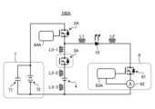
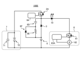
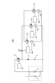
図1は、実施の形態1に係る発光素子駆動回路100の構成を示す回路図である。発光素子駆動回路100は、LD10と、金属酸化膜半導体電界効果型トランジスタ(Metal-Oxide-Semiconductor Field-Effect Transistor:MOSFET)2Aと、MOSFET2Aを駆動するための駆動部64Aと、逆流防止素子であるダイオード3と、第1の直流電源であるブースト電圧源7と、第2の直流電源である主電圧源4と、リニアレギュレータ6と、を備える。リニアレギュレータ6は、LD10に流れる電流を制御する構成要素として、MOSFET61と、第1の電流検出器である電流検出器62と、MOSFET61を駆動するための駆動部63Aとを備える。ブースト電圧源7は、電荷蓄積素子であるコンデンサ71と、電圧源72とを備える。コンデンサ71は、電圧源72の両端に接続される。なお、本稿では、MOSFET2Aを「第1のスイッチ素子」と記載し、MOSFET61を「第2のスイッチ素子」と記載することがある。Embodiment 1.
1 is a circuit diagram showing a configuration of a light-emittingelement drive circuit 100 according to a first embodiment. The light-emitting element drive circuit 100 includes an LD 10, a metal-oxide-semiconductor field-effect transistor (MOSFET) 2A, a drive unit 64A for driving the MOSFET 2A, a diode 3 as a backflow prevention element, a boost voltage source 7 as a first DC power source, a main voltage source 4 as a second DC power source, and a linear regulator 6. The linear regulator 6 includes a MOSFET 61, a current detector 62 as a first current detector, and a drive unit 63A for driving the MOSFET 61 as components for controlling the current flowing through the LD 10. The boost voltage source 7 includes a capacitor 71 as a charge storage element, and a voltage source 72. The capacitor 71 is connected to both ends of the voltage source 72. In this document, MOSFET 2A may be referred to as a "first switch element," and MOSFET 61 may be referred to as a "second switch element."
図1は、実施の形態1に係る発光素子駆動回路100の構成を示す回路図である。発光素子駆動回路100は、LD10と、金属酸化膜半導体電界効果型トランジスタ(Metal-Oxide-Semiconductor Field-Effect Transistor:MOSFET)2Aと、MOSFET2Aを駆動するための駆動部64Aと、逆流防止素子であるダイオード3と、第1の直流電源であるブースト電圧源7と、第2の直流電源である主電圧源4と、リニアレギュレータ6と、を備える。リニアレギュレータ6は、LD10に流れる電流を制御する構成要素として、MOSFET61と、第1の電流検出器である電流検出器62と、MOSFET61を駆動するための駆動部63Aとを備える。ブースト電圧源7は、電荷蓄積素子であるコンデンサ71と、電圧源72とを備える。コンデンサ71は、電圧源72の両端に接続される。なお、本稿では、MOSFET2Aを「第1のスイッチ素子」と記載し、MOSFET61を「第2のスイッチ素子」と記載することがある。
1 is a circuit diagram showing a configuration of a light-emitting
LD10は、発光素子の一例である。LD10のアノードは、MOSFET2Aのソースとダイオード3のカソードとの接続点に接続される。LD10のカソードは、MOSFET61のドレインに接続される。なお、図1では、LD10を単一の素子として図示しているが、単一の素子には限定されない。LD10は、複数の素子が直列又は直並列に接続されるものであってもよい。
LD10 is an example of a light-emitting element. The anode of LD10 is connected to the connection point between the source of MOSFET 2A and the cathode of diode 3. The cathode of LD10 is connected to the drain of MOSFET 61. Note that, although LD10 is illustrated as a single element in FIG. 1, it is not limited to a single element. LD10 may be a plurality of elements connected in series or series-parallel.
ダイオード3のアノードは、主電圧源4の正極に接続される。MOSFET2Aのドレインは、ブースト電圧源7の正極に接続される。MOSFET61のソースは、電流検出器62を介して主電圧源4の負極に接続され、その接続点はブースト電圧源7の負極に接続される。
The anode of diode 3 is connected to the positive electrode of main voltage source 4. The drain of MOSFET 2A is connected to the positive electrode of boost voltage source 7. The source of MOSFET 61 is connected to the negative electrode of main voltage source 4 via current detector 62, and the connection point is connected to the negative electrode of boost voltage source 7.
なお、図1では、電圧源は主電圧源4とブースト電圧源7との2つで図示しているが、それぞれの電圧源は1つずつに限定されない。即ち、主電圧源4は2以上であってもよいし、ブースト電圧源7も2以上であってもよい。主電圧源4及びブースト電圧源7のうちの少なくとも1つの電圧源を増やすことで、負荷の状況に応じた出力が可能となり、より安定した制御が可能となる。
In FIG. 1, two voltage sources are shown, the main voltage source 4 and the boost voltage source 7, but the number of each is not limited to one. That is, there may be two or more main voltage sources 4, and two or more boost voltage sources 7. By increasing the number of at least one of the main voltage sources 4 and the boost voltage source 7, it becomes possible to output according to the load conditions, enabling more stable control.
LD10の両側には、配線インダクタンスL1,L2が示されている。配線インダクタンスL1はダイオード3のカソードとMOSFET2Aのソースとの接続点とLD10のアノードとの間の電気配線のインダクタンスであり、配線インダクタンスL2は主電圧源4の負極とLD10のカソードとの間の電気配線のインダクタンスである。また、ダイオード3及び主電圧源4の両端には、配線インダクタンスL3-1,L3-2,L3-3が示されている。
Wiring inductances L1 and L2 are shown on both sides of LD10. Wiring inductance L1 is the inductance of the electrical wiring between the connection point between the cathode of diode 3 and the source of MOSFET 2A and the anode of LD10, while wiring inductance L2 is the inductance of the electrical wiring between the negative pole of main voltage source 4 and the cathode of LD10. In addition, wiring inductances L3-1, L3-2, and L3-3 are shown on both ends of diode 3 and main voltage source 4.
配線インダクタンスL3-1は、MOSFET2AのソースとLD10のアノードとの接続点とダイオード3のカソードとの間の電気配線のインダクタンスである。配線インダクタンスL3-2は、ダイオード3のアノードと主電圧源4の正極との間の電気配線のインダクタンスである。配線インダクタンスL3-3は、主電圧源4の負極とブースト電圧源7の負極とリニアレギュレータ6との接続点との間の電気配線のインダクタンスである。
Wiring inductance L3-1 is the inductance of the electrical wiring between the connection point between the source of MOSFET 2A and the anode of LD10 and the cathode of diode 3. Wiring inductance L3-2 is the inductance of the electrical wiring between the anode of diode 3 and the positive electrode of main voltage source 4. Wiring inductance L3-3 is the inductance of the electrical wiring between the connection point between the negative electrode of main voltage source 4 and the negative electrode of boost voltage source 7 and linear regulator 6.
次に、上記のように接続された実施の形態1に係る発光素子駆動回路100の回路構成の特徴について説明する。ブースト電圧源7は、第1電圧を保持し、MOSFET2Aを介してLD10のアノードに第1電圧を印加可能に接続されている。主電圧源4は、第1電圧よりも低い第2電圧を保持し、LD10のアノードに第2電圧を印加可能に接続されている。ダイオード3は、第1電圧が主電圧源4へ印加されるのを防止する向きに接続されている。MOSFET2Aは、LD10のアノードに対する第1電圧の印加のオンオフを切り替える。リニアレギュレータ6は、LD10に流れる電流を制御する。MOSFET61には、LD10に流れる電流が通流する。電流検出器62は、MOSFET61に流れる電流を検出することで、LD10に流れる電流を検出する。駆動部63Aは、電流検出器62の検出値に基づいて、MOSFET61を駆動する。
Next, the characteristics of the circuit configuration of the light-emitting element drive circuit 100 according to the first embodiment connected as described above will be described. The boost voltage source 7 holds a first voltage and is connected to the anode of the LD 10 via the MOSFET 2A so that the first voltage can be applied thereto. The main voltage source 4 holds a second voltage lower than the first voltage and is connected to the anode of the LD 10 so that the second voltage can be applied thereto. The diode 3 is connected in a direction that prevents the first voltage from being applied to the main voltage source 4. The MOSFET 2A switches the application of the first voltage to the anode of the LD 10 on and off. The linear regulator 6 controls the current flowing through the LD 10. The current flowing through the LD 10 flows through the MOSFET 61. The current detector 62 detects the current flowing through the LD 10 by detecting the current flowing through the MOSFET 61. The drive unit 63A drives the MOSFET 61 based on the detection value of the current detector 62.
図2は、実施の形態1の変形例に係る発光素子駆動回路100Aの構成を示す回路図である。図2では、図1に示すダイオード3がMOSFET3Aに置き替えられている。その他の構成は、図1の構成と同一又は同等であり、同一又は同等の構成要素には同一の符号を付して示すと共に、重複する説明は割愛する。
FIG. 2 is a circuit diagram showing the configuration of a light-emitting element drive circuit 100A according to a modified example of the first embodiment. In FIG. 2, the diode 3 shown in FIG. 1 is replaced with a MOSFET 3A. The other configuration is the same as or equivalent to the configuration in FIG. 1, and the same or equivalent components are denoted by the same reference numerals and will not be described again.
MOSFET3Aは、逆並列接続ダイオードを備えたスイッチ素子の一例である。逆並列とは、ダイオード部のアノードがMOSFET3Aのソースに接続され、ダイオード部のカソードがMOSFET3Aのドレインに接続されることを意味する。逆並列接続ダイオードの向きは、ダイオード3の向きと同一であり、逆流防止素子として動作する。逆並列接続ダイオードは、外部接続のダイオードでもよいし、MOSFET3Aが内部に有する寄生ダイオードでもよい。寄生ダイオードは、ボディダイオードとも呼ばれる。寄生ダイオードを利用すれば、個別のダイオードが不要になるので、部品点数を削減することができ、コスト低減につながる。
MOSFET3A is an example of a switch element equipped with an anti-parallel connected diode. Anti-parallel means that the anode of the diode part is connected to the source of MOSFET3A, and the cathode of the diode part is connected to the drain of MOSFET3A. The orientation of the anti-parallel connected diode is the same as that of diode 3, and it acts as a reverse current prevention element. The anti-parallel connected diode may be an externally connected diode, or it may be a parasitic diode that MOSFET3A has inside. The parasitic diode is also called a body diode. If a parasitic diode is used, a separate diode is not required, so the number of parts can be reduced, leading to cost reduction.
MOSFET3Aに対しては、逆並列接続ダイオードに電流が流れるタイミングでMOSFET3Aをオン動作させる同期整流制御を実施してもよい。MOSFET3Aに対して同期整流制御を実施すれば、回路損失の更なる低減が可能となり、電源効率を高めることができる。
Synchronous rectification control may be performed on MOSFET 3A, which turns on MOSFET 3A when current flows through the anti-parallel connected diode. By performing synchronous rectification control on MOSFET 3A, it becomes possible to further reduce circuit loss and improve power supply efficiency.
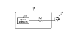
図3は、図1に示す駆動部63Aの一般的な構成例を示す回路図である。図3には、駆動部63Aと共に、MOSFET61及び電流検出器62が示されている。
FIG. 3 is a circuit diagram showing a typical configuration example of the drive unit 63A shown in FIG. 1. In FIG. 3, a MOSFET 61 and a current detector 62 are shown together with the drive unit 63A.
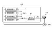
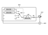
「定数回路1又は2」という表記は、「定数回路1」又は「定数回路2」の何れか1つが配置されることを意味する。従来から使用されている駆動部63Aの構成は、図3に示すように、定数回路は1つしか有さない構成が一般的である。
The notation " constant circuit 1 or 2" means that either "constant circuit 1" or "constant circuit 2" is arranged. The configuration of the drive unit 63A that has been used conventionally generally has only one constant circuit, as shown in FIG. 3.
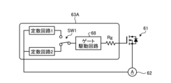
1つの定数回路は、ゲート駆動回路68に接続される。ゲート駆動回路68は、MOSFET61のゲートを駆動する回路であり、ゲート抵抗Rgを介してMOSFET61に接続される。定数回路は、例えば誤差増幅器、エラーアンプ回路であり、基準電圧と、MOSFET61に流れる電流から導かれた帰還電圧とを比較して、MOSFET61のゲート電圧が所望の電圧になるように制御する回路である。本稿では、定数回路1によって設定される制御定数を「制御定数1」と表記し、定数回路2によって設定される制御定数を「制御定数2」と表記する。
One constant circuit is connected to gate drive circuit 68. Gate drive circuit 68 is a circuit that drives the gate of MOSFET 61, and is connected to MOSFET 61 via gate resistor Rg. The constant circuit is, for example, an error amplifier, and is a circuit that compares a reference voltage with a feedback voltage derived from the current flowing through MOSFET 61, and controls the gate voltage of MOSFET 61 to a desired voltage. In this paper, the control constant set by constant circuit 1 is referred to as "control constant 1", and the control constant set by constant circuit 2 is referred to as "control constant 2".
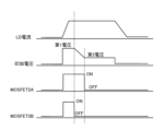
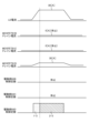
[発明が解決しようとする課題]の項でも説明したが、高電圧源から低電圧源への切替時では、LDに流れる電流であるLD電流の速度変化が大きいので、制御が不安定になり、LD電流が発振するおそれがあった。例えば、LD電流の立ち上がりを高速化するための第1電圧(高電圧)で制御定数を設定すると、立ち上がり後の損失低減のために切り替える第2電圧(低電圧)のときに制御が不安定になり発振し易くなる。逆に、第2電圧で制御定数を設定すると、立ち上がり時の制御が不安定になりオーバーシュートや発振が生じ易い。この現象は、第1電圧での制御で必要となる応答性が100us以下のオーダーであるのに対し、第2電圧での制御では100ms以下のオーダーでの応答性でよいという制御特性に起因している。即ち、印加電圧の切替前後における制御の応答性に、大きな差があることが要因である。
As explained in the section on "Problems to be Solved by the Invention," when switching from a high voltage source to a low voltage source, the speed of the LD current, which is the current flowing through the LD, changes significantly, which can cause the control to become unstable and the LD current to oscillate. For example, if the control constant is set at the first voltage (high voltage) to speed up the rise of the LD current, the control becomes unstable and oscillation becomes more likely when the second voltage (low voltage) is switched to reduce losses after the rise. Conversely, if the control constant is set at the second voltage, the control becomes unstable at the time of rise, and overshoot and oscillation are likely to occur. This phenomenon is due to the control characteristics in which the responsiveness required for control at the first voltage is on the order of 100 us or less, while the responsiveness required for control at the second voltage is on the order of 100 ms or less is sufficient. In other words, the cause is a large difference in the responsiveness of the control before and after switching the applied voltage.
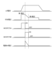
図4は、図3の駆動部63Aを使用して制御した場合の動作説明に供する第1のタイムチャートである。図5は、図3の駆動部63Aを使用して制御した場合の動作説明に供する第2のタイムチャートである。
FIG. 4 is a first time chart used to explain the operation when control is performed using the drive unit 63A in FIG. 3. FIG. 5 is a second time chart used to explain the operation when control is performed using the drive unit 63A in FIG. 3.
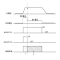
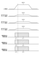
具体的に、図4は、第1電圧に合わせて設定した制御定数1を有する定数回路1を、第2電圧の印加時にも使用したときのタイムチャートである。一方、図5は、第2電圧に合わせて設定した制御定数2を有する定数回路2を、第1電圧の印加時にも使用したときのタイムチャートである。図4及び図5の両図共に、各波形は、上段側から、LD電流、印加電圧、MOSFET61の動作状態、MOSFET2Aの動作状態、及び設定される制御定数を表している。LD電流はLD10に流れる電流であり、印加電圧はLD10のアノードと主電圧源4の負極との電圧である。また、MOSFET動作状態は、各MOSFETへのゲート・ソース間電圧をイメージした各MOSFETの動作状態を示している。また、両図の横軸は時間を表している。また、制御定数の差異は、数値及びハッチングパターンの差異で表している。具体的に、「1」は、制御定数1を意味し、「2」は、制御定数2を意味している。なお、MOSFET2Aのオンオフは、駆動部63Aではなく、駆動部64Aによって制御される。駆動部63A,64Aについては、これらを符号無しでも区別できるように、駆動部64Aについては、「第2の駆動部64A」又は符号を省略して「第2の駆動部」と記載することがある。
Specifically, FIG. 4 is a time chart when the constant circuit 1 having the control constant 1 set according to the first voltage is used when the second voltage is applied. On the other hand, FIG. 5 is a time chart when the constant circuit 2 having the control constant 2 set according to the second voltage is used when the first voltage is applied. In both FIG. 4 and FIG. 5, the waveforms represent, from the top, the LD current, the applied voltage, the operating state of MOSFET 61, the operating state of MOSFET 2A, and the set control constant. The LD current is the current flowing through LD 10, and the applied voltage is the voltage between the anode of LD 10 and the negative pole of the main voltage source 4. The MOSFET operating state shows the operating state of each MOSFET, which is an image of the gate-source voltage to each MOSFET. The horizontal axis of both figures represents time. The difference in the control constants is represented by the difference in the numerical value and the hatching pattern. Specifically, "1" means the control constant 1, and "2" means the control constant 2. The on/off of MOSFET 2A is controlled by drive unit 64A, not drive unit 63A. To allow drive units 63A and 64A to be distinguished without reference numbers, drive unit 64A may be referred to as the "second drive unit 64A" or the "second drive unit" without the reference number.
図4の場合、第2電圧の印加時にLD電流が発振する様子が示されている。これは、第1電圧に合わせて設定した制御定数1を第2電圧の印加時にも使用しているためである。また、図5の場合、第1電圧の印加時にLD電流が発振する様子が示されている。これは、第2電圧に合わせて設定した制御定数2を第1電圧の印加時にも使用しているためである。
In the case of Figure 4, the LD current is shown oscillating when the second voltage is applied. This is because control constant 1, which is set to match the first voltage, is also used when the second voltage is applied. In addition, in the case of Figure 5, the LD current is shown oscillating when the first voltage is applied. This is because control constant 2, which is set to match the second voltage, is also used when the first voltage is applied.
LD電流が発振すると、LD10の発光強度にムラが生じ、LD10の寿命にも影響する。LDの適用製品が、例えばレーザー加工機等である場合、加工品質に影響を与える。これらの課題を解決するためには、例えば、第1電圧及び第2電圧のそれぞれに合わせてリニアレギュレータ6を2つ用意するという方法が考えられる。しかしながら、この考え方では、MOSFET61、電流検出器62及び駆動部63Aもそれぞれ2つ必要となるので、回路面積及び部品点数が増加し、製品の大型化及びコストアップは不可避となる。また、2つのリニアレギュレータ6の間で起こり得る相互共振の課題もあり、共振対策に要する設計工数の増加も問題となる。
When the LD current oscillates, unevenness occurs in the light emission intensity of the LD 10, which also affects the lifespan of the LD 10. If the product to which the LD is applied is, for example, a laser processing machine, this affects the processing quality. To solve these problems, for example, it is possible to consider a method of preparing two linear regulators 6 for each of the first and second voltages. However, with this approach, two MOSFETs 61, two current detectors 62, and two drive units 63A are also required, which increases the circuit area and number of parts, making it inevitable that the product will become larger and more expensive. There is also the issue of mutual resonance that can occur between the two linear regulators 6, and the increase in design man-hours required to deal with the resonance will also be a problem.
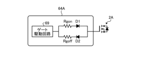
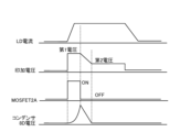
そこで、実施の形態1では、図6に示す構成を提案する。図6は、実施の形態1に係る駆動部63Aの構成を示す回路図である。図3と同一又は同等の構成要素には、同一の符号を付して示している。図6に示すように、駆動部63Aは、第1電圧に対応した定数回路1及び第2電圧に対応した定数回路2を備えると共に、定数回路1及び定数回路2のうちの1つを選択してゲート駆動回路68に接続するスイッチ機構SW1を備えている。スイッチ機構SW1は、LD10への印加電圧が第1電圧であるか第2電圧であるかに応じて、定数回路1側、又は定数回路2側の何れかに切り替えられる。
Therefore, in the first embodiment, the configuration shown in FIG. 6 is proposed. FIG. 6 is a circuit diagram showing the configuration of a drive unit 63A according to the first embodiment. Components that are the same as or equivalent to those in FIG. 3 are shown with the same reference numerals. As shown in FIG. 6, the drive unit 63A includes a constant circuit 1 corresponding to a first voltage and a constant circuit 2 corresponding to a second voltage, as well as a switch mechanism SW1 that selects one of the constant circuits 1 and 2 and connects it to the gate drive circuit 68. The switch mechanism SW1 is switched to either the constant circuit 1 side or the constant circuit 2 side depending on whether the voltage applied to the LD 10 is the first voltage or the second voltage.
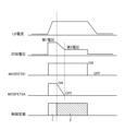
図7は、図6の駆動部63Aを使用して制御した場合の動作説明に供するタイムチャートである。波形の種類及び表記の仕方は、図4及び図5と同一である。図7によれば、第2電圧の印加直後にLD電流が落ち込む現象が見られるものの、第1電圧及び第2電圧の印加時共に、安定したLD電流が流れていることが分かる。
FIG. 7 is a time chart explaining the operation when controlled using the driving unit 63A in FIG. 6. The types of waveforms and the notation are the same as in FIG. 4 and FIG. 5. According to FIG. 7, although a phenomenon in which the LD current drops immediately after the application of the second voltage is observed, it can be seen that a stable LD current flows when both the first voltage and the second voltage are applied.
以上説明したように、実施の形態1に係る発光素子駆動回路は、第1及び第2の直流電源、第1のスイッチ素子、逆流防止素子、及び発光素子に流れる電流を制御するリニアレギュレータを備える。第1の直流電源は、第1電圧を保持し、発光素子のアノードに第1電圧を印加可能に接続される。第2の直流電源は、発光素子のアノードに第1電圧よりも低い第2電圧を印加可能に接続される。第1のスイッチ素子は、発光素子のアノードに対する第1電圧の印加のオンオフを切り替える。逆流防止素子は、第1電圧が第2の直流電源へ印加されるのを防止する向きに接続される。また、リニアレギュレータは、発光素子に流れる電流を検出する電流検出器と、発光素子に流れる電流が通流する第2のスイッチ素子と、第2のスイッチ素子を駆動する駆動部とを備える。駆動部は、第2のスイッチ素子のゲートを駆動するゲート駆動回路と、互いに異なる制御定数が設定される2つの定数回路と、発光素子への印加電圧が第1電圧であるか第2電圧であるかに応じて、2つの定数回路のうちの1つを選択してゲート駆動回路に接続するスイッチ機構とを備える。このように構成された発光素子駆動回路において、例えば発光素子への印加電圧が第1電圧である場合、スイッチ機構は、2つの定数回路のうちの一方を選択するように動作し、発光素子への印加電圧が第2電圧である場合、スイッチ機構は、定数回路の選択を切り替えて2つの定数回路のうちのもう一方を選択するように動作する。これにより、発光素子駆動回路は、印加電圧に適した定数回路は選択されるので、第1電圧及び第2電圧共に安定したLD電流を流すことが可能となり、LDをオンした直後のLD電流の立ち上がりの高速化と制御の安定性とを両立することが可能となる。
As described above, the light-emitting element driving circuit of embodiment 1 includes first and second DC power sources, a first switch element, a backflow prevention element, and a linear regulator that controls the current flowing through the light-emitting element. The first DC power source holds a first voltage and is connected so as to be able to apply the first voltage to the anode of the light-emitting element. The second DC power source is connected so as to be able to apply a second voltage lower than the first voltage to the anode of the light-emitting element. The first switch element switches on and off the application of the first voltage to the anode of the light-emitting element. The backflow prevention element is connected in a direction that prevents the first voltage from being applied to the second DC power source. The linear regulator also includes a current detector that detects the current flowing through the light-emitting element, a second switch element through which the current flowing through the light-emitting element flows, and a drive unit that drives the second switch element. The driving unit includes a gate driving circuit that drives the gate of the second switch element, two constant circuits in which different control constants are set, and a switch mechanism that selects one of the two constant circuits and connects it to the gate driving circuit depending on whether the voltage applied to the light-emitting element is the first voltage or the second voltage. In the light-emitting element driving circuit configured in this manner, for example, when the voltage applied to the light-emitting element is the first voltage, the switch mechanism operates to select one of the two constant circuits, and when the voltage applied to the light-emitting element is the second voltage, the switch mechanism operates to switch the selection of the constant circuit and select the other of the two constant circuits. As a result, the light-emitting element driving circuit selects a constant circuit suitable for the applied voltage, making it possible to flow a stable LD current for both the first and second voltages, and making it possible to achieve both a faster rise in the LD current immediately after turning on the LD and stable control.
また、実施の形態1に係る発光素子駆動回路によれば、リニアレギュレータを増設することなく1つのリニアレギュレータで対応できるので、回路面積及び部品点数の増加を抑制することができ、製品の大型化及び製造コストの上昇を回避することが可能となる。また、リニアレギュレータが1つであるため、2つのリニアレギュレータ間で起こり得る相互共振に要する対策が不要になるので、開発工数の削減も見込める。以上により、設計コスト及び製造コストの増加、並びに製品の大型化を抑制しながら、製品の性能向上を図ることが可能となる。
Furthermore, according to the light-emitting element drive circuit of embodiment 1, a single linear regulator is sufficient without the need to add additional linear regulators, so that an increase in circuit area and number of components can be suppressed, and it becomes possible to avoid an increase in product size and manufacturing costs. Furthermore, since there is only one linear regulator, measures required for mutual resonance that can occur between the two linear regulators are not necessary, so a reduction in development labor is expected. As a result, it becomes possible to improve product performance while suppressing increases in design costs and manufacturing costs, as well as an increase in product size.
なお、実施の形態1では、定数回路の数を2としているが、3以上であってもよい。第1及び第2の直流電源のうちの少なくとも1つが2以上の電圧源を有している場合、この電源構成に対応させて、定数回路の数を3以上としてもよい。
In the first embodiment, the number of constant circuits is two, but it may be three or more. If at least one of the first and second DC power supplies has two or more voltage sources, the number of constant circuits may be three or more in accordance with this power supply configuration.
実施の形態2.
前述したように、図7に示す動作波形では、第2電圧の印加直後にLD電流が落ち込む現象が観察される。このLD電流の落ち込みは、図1に示される配線インダクタンスL3-1,L3-2,L3-3が存在することによって引き起こされると考えられる。配線インダクタンスL3-1,L3-2,L3-3に限らず、インダクタンスには、急激な電流上昇を抑制するという特性がある。第1電圧を印加してLD10への通電を開始しても、配線インダクタンスL3-1,L3-2,L3-3には、LD電流が流れていない。このため、第1電圧から第2電圧への切り替え直後では、配線インダクタンスL3-1,L3-2,L3-3に生じる逆起電力によってLD電流が直ぐには追従できず、図示のような落ち込みが発生することになる。実施の形態2では、この課題に対する解決策を提示する。Embodiment 2.
As mentioned above, in the operating waveform shown in FIG. 7, a phenomenon is observed in which the LD current drops immediately after the application of the second voltage. It is believed that this drop in the LD current is caused by the presence of the wiring inductances L3-1, L3-2, and L3-3 shown in FIG. 1. Inductances, including wiring inductances L3-1, L3-2, and L3-3, have the characteristic of suppressing a sudden current rise. Even if the first voltage is applied to start energizing theLD 10, no LD current flows through the wiring inductances L3-1, L3-2, and L3-3. Therefore, immediately after switching from the first voltage to the second voltage, the LD current cannot immediately follow due to the back electromotive force generated in the wiring inductances L3-1, L3-2, and L3-3, and a drop occurs as shown in the figure. In the second embodiment, a solution to this problem is presented.
前述したように、図7に示す動作波形では、第2電圧の印加直後にLD電流が落ち込む現象が観察される。このLD電流の落ち込みは、図1に示される配線インダクタンスL3-1,L3-2,L3-3が存在することによって引き起こされると考えられる。配線インダクタンスL3-1,L3-2,L3-3に限らず、インダクタンスには、急激な電流上昇を抑制するという特性がある。第1電圧を印加してLD10への通電を開始しても、配線インダクタンスL3-1,L3-2,L3-3には、LD電流が流れていない。このため、第1電圧から第2電圧への切り替え直後では、配線インダクタンスL3-1,L3-2,L3-3に生じる逆起電力によってLD電流が直ぐには追従できず、図示のような落ち込みが発生することになる。実施の形態2では、この課題に対する解決策を提示する。
As mentioned above, in the operating waveform shown in FIG. 7, a phenomenon is observed in which the LD current drops immediately after the application of the second voltage. It is believed that this drop in the LD current is caused by the presence of the wiring inductances L3-1, L3-2, and L3-3 shown in FIG. 1. Inductances, including wiring inductances L3-1, L3-2, and L3-3, have the characteristic of suppressing a sudden current rise. Even if the first voltage is applied to start energizing the
図8は、図1に示す第2の駆動部64Aの一般的な構成例である第2の駆動部64の回路構成を示す図である。図8には、第2の駆動部64と共に、MOSFET2Aが示されている。第2の駆動部64は、ゲート駆動回路69と、ゲート抵抗Rg1とを備える。ゲート駆動回路69は、MOSFET2Aのゲートを駆動する回路であり、ゲート抵抗Rg1を介してMOSFET2Aに接続されている。
FIG. 8 is a diagram showing the circuit configuration of the second drive unit 64, which is a typical example of the second drive unit 64A shown in FIG. 1. FIG. 8 shows MOSFET 2A together with the second drive unit 64. The second drive unit 64 includes a gate drive circuit 69 and gate resistor Rg1. The gate drive circuit 69 is a circuit that drives the gate of MOSFET 2A, and is connected to MOSFET 2A via gate resistor Rg1.
また、図9は、実施の形態2に係る第2の駆動部64Aの構成を示す回路図である。図8と同一又は同等の構成要素には、同一の符号を付して示している。第2の駆動部64Aは、図9に示すように、ゲート駆動回路69と、ゲート抵抗Rgon,Rgoffと、ダイオードD1,D2とを備えている。ダイオードD1,D2には同一又は同等の特性のものが用いられる。
FIG. 9 is a circuit diagram showing the configuration of a second drive unit 64A according to the second embodiment. Components that are the same as or equivalent to those in FIG. 8 are denoted with the same reference numerals. As shown in FIG. 9, the second drive unit 64A includes a gate drive circuit 69, gate resistors Rgon and Rgoff, and diodes D1 and D2. Diodes D1 and D2 have the same or equivalent characteristics.
ゲート駆動回路69は、ゲート抵抗Rgon及びダイオードD1を介してMOSFET2Aのゲート容量に電荷を注入することでMOSFET2Aをオンする。また、ゲート駆動回路69は、ゲート抵抗Rgoff及びダイオードD2を介してMOSFET2Aのゲート容量に蓄積された電荷を引き抜くことでMOSFET2Aをオフする。また、ゲート抵抗Rgon,Rgoff間には、(Rgonの抵抗値)<(Rgoffの抵抗値)の関係がある。このような第2の駆動部64Aを用いると、MOSFET2Aをゲートオンするときの駆動速度は、MOSFET2Aをゲートオフするときの駆動速度よりも速くなる。言い替えると、MOSFET2Aをゲートオフするときの駆動速度は、MOSFET2Aをゲートオンするときの駆動速度よりも遅くなる。
The gate drive circuit 69 turns on MOSFET 2A by injecting charge into the gate capacitance of MOSFET 2A via gate resistor Rgon and diode D1. The gate drive circuit 69 also turns off MOSFET 2A by extracting charge accumulated in the gate capacitance of MOSFET 2A via gate resistor Rgoff and diode D2. There is a relationship between the gate resistors Rgon and Rgoff such that (resistance value of Rgon) < (resistance value of Rgoff). When such a second drive unit 64A is used, the drive speed when gating on MOSFET 2A is faster than the drive speed when gating off MOSFET 2A. In other words, the drive speed when gating off MOSFET 2A is slower than the drive speed when gating on MOSFET 2A.
図10は、図9の第2の駆動部64Aを使用して制御した場合の動作説明に供するタイムチャートである。波形の種類及び表記の仕方は、他のタイムチャートの図と同じである。図10の印加電圧の波形を図7のものと比較すると、図10の場合には、印加電圧の立ち下がりが緩やかになっている。これは、図10のMOSFET2Aの動作波形の立ち上がり部と立ち下がり部とを比較すれば分かるように、MOSFET2Aをゲートオフするときの駆動速度がMOSFET2Aをゲートオンするときの駆動速度よりも遅いためである。その結果、ブースト電圧源7からの電流供給がゆっくりと遮断されていくので、主電圧源4によるLD10への電流供給が間に合うようになる。これにより、図10のLD電流の波形を図7のものと比較すれば分かるように、LD電流の落ち込みを解消、もしくは小さくすることができる。
FIG. 10 is a time chart for explaining the operation when the second driving unit 64A in FIG. 9 is used for control. The types of waveforms and the way of notation are the same as those in the other time charts. Comparing the waveform of the applied voltage in FIG. 10 with that in FIG. 7, the applied voltage in FIG. 10 falls more gently. This is because, as can be seen by comparing the rising and falling parts of the operating waveform of MOSFET 2A in FIG. 10, the driving speed when gate-off MOSFET 2A is slower than the driving speed when gate-on MOSFET 2A. As a result, the current supply from the boost voltage source 7 is cut off slowly, so that the current supply to LD 10 by the main voltage source 4 is in time. This makes it possible to eliminate or reduce the drop in LD current, as can be seen by comparing the waveform of the LD current in FIG. 10 with that in FIG. 7.
上記で説明した第2の駆動部64Aによる機能を、本稿では「電圧変化緩和手段」と呼ぶ。電圧変化緩和手段は、LD10への印加電圧が第1電圧(高電圧)から第2電圧(低電圧)へ切り替わるときに、LD10への印加電圧の変化を緩和する機能を実現する手段である。図10では、第1の実施例として、電圧変化緩和手段を第2の駆動部64Aの内部に設ける例を説明した。
The function provided by the second drive unit 64A described above is referred to as the "voltage change mitigation means" in this document. The voltage change mitigation means is a means for realizing the function of mitigating the change in the voltage applied to the LD 10 when the voltage applied to the LD 10 switches from a first voltage (high voltage) to a second voltage (low voltage). In FIG. 10, as a first embodiment, an example in which the voltage change mitigation means is provided inside the second drive unit 64A is described.
なお、第2の駆動部64Aを使用するとき、MOSFET2Aとしては、プレーナー構造のMOSFETを使用するのが好ましい実施例となる。以下、その理由について説明する。
When using the second driving unit 64A, it is preferable to use a planar MOSFET as the MOSFET 2A. The reasons for this are explained below.
MOSFETのオン速度及びオフ速度は、MOSFETの電圧増幅度、ゲート容量及びゲート抵抗に依存している。そして、電圧増幅度及びゲート容量は、MOSFETの構造に依存している。具体的に、電圧増幅度は、(トレンチ構造の電圧増幅度)>(プレーナー構造の電圧増幅度)という関係であることが一般的である。また、ゲート容量は、(トレンチ構造のゲート容量)<(プレーナー構造のゲート容量)という関係であることが一般的である。
The on-speed and off-speed of a MOSFET depend on the voltage amplification, gate capacitance, and gate resistance of the MOSFET. The voltage amplification and gate capacitance depend on the structure of the MOSFET. Specifically, the voltage amplification generally has the relationship (voltage amplification of trench structure) > (voltage amplification of planar structure). The gate capacitance generally has the relationship (gate capacitance of trench structure) < (gate capacitance of planar structure).
即ち、トレンチ構造のMOSFETとプレーナー構造のMOSFETとを比較すると、トレンチ構造のMOSFETは、構造由来の電圧増幅度が相対的に大きく、且つゲート容量が小さい。従って、トレンチ構造のMOSFETは、ゲート抵抗によるゲート容量への充放電時間の影響が小さく、且つ電圧増幅度が大きいので、MOSFETをオンするときのゲート印加電圧の変化幅は小さくてよい。なお、変化幅が小さいことは、オン速度及びオフ速度の調整の感度が小さいことを意味している。
In other words, when comparing a trench-structure MOSFET with a planar-structure MOSFET, the trench-structure MOSFET has a relatively large voltage amplification due to its structure and a small gate capacitance. Therefore, in a trench-structure MOSFET, the effect of the charge/discharge time on the gate capacitance due to the gate resistance is small, and the voltage amplification is large, so the change range of the gate applied voltage when turning on the MOSFET can be small. Furthermore, a small change range means that the sensitivity of adjusting the on-speed and off-speed is low.
これに対し、プレーナー構造のMOSFETは、構造由来の電圧増幅度が相対的に小さく、且つゲート容量が大きい。従って、プレーナー構造のMOSFETは、ゲート抵抗によるゲート容量への充放電時間の影響が大きく、且つ電圧増幅度が小さいので、MOSFETをオンするときのゲート印加電圧の変化幅を大きくする必要がある。このことは、オン速度及びオフ速度の調整の感度が大きく、速度の調整がトレンチ構造よりも容易であることを意味している。従って、MOSFET2Aとしてプレーナー構造のものを使用すれば、電圧変化緩和手段の効果を容易に得ることが可能となる。
In contrast, a planar-structure MOSFET has a relatively small voltage amplification due to its structure and a large gate capacitance. Therefore, in a planar-structure MOSFET, the charge/discharge time on the gate capacitance due to the gate resistance is significantly affected, and the voltage amplification is small, so it is necessary to increase the range of change in the gate applied voltage when turning on the MOSFET. This means that the sensitivity of adjusting the on and off speeds is high, and speed adjustment is easier than with a trench structure. Therefore, if a MOSFET with a planar structure is used for MOSFET 2A, it becomes possible to easily obtain the effect of the voltage change mitigation means.
次に、電圧変化緩和手段の他の実施例について、図11及び図12を参照して説明する。まず、図11は、実施の形態2に係る発光素子駆動回路100Bの構成を示す回路図である。
Next, other examples of voltage change mitigation means will be described with reference to Figures 11 and 12. First, Figure 11 is a circuit diagram showing the configuration of a light-emitting element drive circuit 100B according to embodiment 2.
図11に示す実施の形態2に係る発光素子駆動回路100Bと、図1に示す実施の形態1に係る発光素子駆動回路100とを比較すると、図11では、MOSFET2Bと抵抗2Cとの並列回路が追加されている。並列回路は、発光素子駆動回路100Bにおいては、電圧変化緩和手段として動作する。また、図11では、駆動部64Aが駆動部64に変更されている。なお、駆動部64は、駆動部64Aであってもよい。その他の構成は、図1の構成と同一又は同等であり、同一又は同等の構成要素には同一の符号を付して示すと共に、重複する説明は割愛する。なお、本稿では、MOSFET2Bを「第3のスイッチ素子」と記載することがある。
Comparing the light-emitting element drive circuit 100B according to the second embodiment shown in FIG. 11 with the light-emitting element drive circuit 100 according to the first embodiment shown in FIG. 1, a parallel circuit of a MOSFET 2B and a resistor 2C is added in FIG. 11. In the light-emitting element drive circuit 100B, the parallel circuit operates as a voltage change mitigation means. Also, in FIG. 11, the drive unit 64A is changed to the drive unit 64. Note that the drive unit 64 may be the drive unit 64A. The other configurations are the same or equivalent to the configuration in FIG. 1, and the same or equivalent components are denoted by the same reference numerals, and duplicated explanations will be omitted. Note that in this document, the MOSFET 2B may be referred to as the "third switch element."
なお、図11では、並列回路が、LD10とダイオード3との接続点とMOSFET2Aのソースとの間に配置される例を示しているが、これに限定されない。並列回路は、ブースト電圧源7の正極とMOSFET2Aとの間に配置されていてもよい。
Note that, although FIG. 11 shows an example in which the parallel circuit is arranged between the connection point between LD10 and diode 3 and the source of MOSFET 2A, this is not limiting. The parallel circuit may also be arranged between the positive electrode of boost voltage source 7 and MOSFET 2A.
また、図12は、実施の形態2に係る発光素子駆動回路100Bの動作説明に供するタイムチャートである。図12において、各波形は、上段側から、LD電流、印加電圧、MOSFET2Aの動作状態及びMOSFET2Bの動作状態を表し、横軸は時間を表している。
FIG. 12 is a time chart for explaining the operation of the light-emitting element drive circuit 100B according to the second embodiment. In FIG. 12, the waveforms represent, from the top, the LD current, the applied voltage, the operating state of MOSFET 2A, and the operating state of MOSFET 2B, and the horizontal axis represents time.
図12に示すように、MOSFET2A,2Bは同時にオンに制御される。これにより、第1電圧は、MOSFET2A,2Bを介してLD10のアノードに印加される。その後、MOSFET2Bのみがオフに制御される。このとき、MOSFET2Aはオンを継続しているので、第1電圧の印加も継続するが、抵抗2Cを介して印加されるので、LD電流の供給がゆっくりと行われる。その後、印加電圧は、図12に示されるように、第2電圧に向かって徐々に減少していく。以上の動作により、LD電流の落ち込みを解消、もしくは小さくすることができる。なお、MOSFET2Bをオフした際に、抵抗2Cによる電圧降下によって印加電圧が低下することが想定されるが、抵抗2Cは電圧の変化を緩和することが目的であり、抵抗2Cの抵抗値は小さく設定されるので、急激な電圧変化は生じない。この際、MOSFET2Bを緩やかにオフにすれば、更に電圧変化を抑えることができる。なお、抵抗2Cに代えて、インダクタンス成分を有する素子を用いることも可能である。
As shown in FIG. 12, MOSFETs 2A and 2B are simultaneously controlled to be on. As a result, the first voltage is applied to the anode of LD 10 via MOSFETs 2A and 2B. After that, only MOSFET 2B is controlled to be off. At this time, since MOSFET 2A continues to be on, the application of the first voltage also continues, but since it is applied via resistor 2C, the LD current is supplied slowly. After that, the applied voltage gradually decreases toward the second voltage as shown in FIG. 12. By the above operation, the drop in the LD current can be eliminated or reduced. Note that when MOSFET 2B is turned off, it is assumed that the applied voltage will decrease due to the voltage drop caused by resistor 2C, but since the purpose of resistor 2C is to mitigate the voltage change and the resistance value of resistor 2C is set small, no sudden voltage change will occur. At this time, if MOSFET 2B is turned off gradually, the voltage change can be further suppressed. Note that an element having an inductance component can also be used instead of resistor 2C.
なお、MOSFET2Aがオン、MOSFET2Bがオフとなる期間は短時間であり、MOSFET2A,2Bの両者がオンとなる期間中に印加される第1電圧は、抵抗2Cを介さないので、抵抗2Cの発熱が問題なるような状態にはならない。また、必要なLD電流が小さく、且つ、ブースト電圧源7からの電流供給時間が短時間である場合には、抵抗2Cの発熱が問題になるような状態とはならないので、MOSFET2Bを配置せずに省略することも可能である。
Note that the period during which MOSFET 2A is on and MOSFET 2B is off is short, and the first voltage applied during the period during which both MOSFETs 2A and 2B are on does not pass through resistor 2C, so heat generation from resistor 2C does not become a problem. Also, if the required LD current is small and the time for which current is supplied from boost voltage source 7 is short, heat generation from resistor 2C does not become a problem, so it is possible to omit MOSFET 2B.
以上説明したように、実施の形態2に係る発光素子駆動回路は、発光素子への印加電圧が第1電圧から第2電圧へ切り替わるときに、印加電圧の変化を緩和する電圧変化緩和手段を更に備える。電圧変化緩和手段は、第1のスイッチ素子を駆動する第2の駆動部に設けることができる。電圧変化緩和手段は、発光素子への印加電圧が第1電圧から第2電圧へ切り替わるときに、発光素子への印加電圧の変化を緩和するように動作する。これにより、第1の直流電源からの電流供給がゆっくりと遮断され、第2の直流電源による発光素子への電流供給が間に合うようになる。その結果、第2電圧の印加直後に起こり得る発光素子電流の落ち込みを解消、もしくは小さくすることができる。従って、実施の形態2に係る発光素子駆動回路は、実施の形態1の効果であるLD電流の立ち上がりの高速化と制御の安定性との両立を図りつつ、更に定電流駆動時の電流安定性を確保することが可能となる。
As described above, the light-emitting element drive circuit according to the second embodiment further includes a voltage change mitigation means for mitigating the change in the applied voltage when the voltage applied to the light-emitting element switches from the first voltage to the second voltage. The voltage change mitigation means can be provided in the second drive unit that drives the first switch element. The voltage change mitigation means operates to mitigate the change in the applied voltage to the light-emitting element when the voltage applied to the light-emitting element switches from the first voltage to the second voltage. This allows the current supply from the first DC power source to be cut off slowly, and the current supply from the second DC power source to the light-emitting element can be made in time. As a result, the drop in the light-emitting element current that may occur immediately after the application of the second voltage can be eliminated or reduced. Therefore, the light-emitting element drive circuit according to the second embodiment can achieve both the effect of the first embodiment of accelerating the rise of the LD current and the stability of control, while also ensuring current stability during constant current drive.
なお、実施の形態2に係る発光素子駆動回路において、第1のスイッチ素子は、プレーナー構造の金属酸化膜半導体電界効果型トランジスタを用いることができる。プレーナー構造の金属酸化膜半導体電界効果型トランジスタを用いれば、上述した電圧変化緩和手段の効果を容易に得ることが可能となる。
In the light-emitting element drive circuit according to the second embodiment, the first switch element can be a metal oxide semiconductor field effect transistor having a planar structure. By using a metal oxide semiconductor field effect transistor having a planar structure, it is possible to easily obtain the effect of the voltage change mitigation means described above.
また、実施の形態2に係る発光素子駆動回路において、電圧変化緩和手段は、第3のスイッチ素子と、抵抗との並列回路で構成されていてもよい。この並列回路は、発光素子及び逆流防止素子の接続点と第2のスイッチ素子との間、又は、第1の直流電源の正極と第2のスイッチ素子との間に配置することができる。この構成において、第3のスイッチ素子は第1電圧の印加時にオンに制御され、第1電圧から第2電圧への切り替え時にオフに制御される。このように制御することで、上述した電圧変化緩和手段による作用効果を得ることが可能となる。
Furthermore, in the light-emitting element drive circuit according to the second embodiment, the voltage change mitigation means may be configured as a parallel circuit of a third switch element and a resistor. This parallel circuit can be disposed between the connection point of the light-emitting element and the reverse current prevention element and the second switch element, or between the positive pole of the first DC power supply and the second switch element. In this configuration, the third switch element is controlled to be on when the first voltage is applied, and is controlled to be off when switching from the first voltage to the second voltage. By controlling in this manner, it is possible to obtain the action and effect of the voltage change mitigation means described above.
実施の形態3.
実施の形態2の項でも説明したように、図7に示す動作波形では、第2電圧の印加直後にLD電流が落ち込む現象が観察される。このLD電流の落ち込みは、図1に示される配線インダクタンスL3-1,L3-2,L3-3が存在することによって引き起こされると考えられる。配線インダクタンスL3-1,L3-2,L3-3に限らず、インダクタンスには、急激な電流上昇を抑制するという特性がある。第1電圧を印加してLD10への通電を開始しても、配線インダクタンスL3-1,L3-2,L3-3には、LD電流が流れていない。このため、第1電圧から第2電圧への切り替え直後では、配線インダクタンスL3-1,L3-2,L3-3に生じる逆起電力によってLD電流が直ぐには追従できず、図示のような落ち込みが発生することになる。実施の形態3では、この課題に対して、実施の形態2とは異なる解決策を提示する。Embodiment 3.
As explained in the section of the second embodiment, in the operating waveform shown in FIG. 7, a phenomenon in which the LD current drops immediately after the application of the second voltage is observed. This drop in the LD current is thought to be caused by the presence of the wiring inductances L3-1, L3-2, and L3-3 shown in FIG. 1. Inductances, including wiring inductances L3-1, L3-2, and L3-3, have the characteristic of suppressing a sudden current rise. Even if the first voltage is applied to start energizing theLD 10, the LD current does not flow through the wiring inductances L3-1, L3-2, and L3-3. Therefore, immediately after switching from the first voltage to the second voltage, the LD current cannot immediately follow due to the back electromotive force generated in the wiring inductances L3-1, L3-2, and L3-3, and a drop occurs as shown in the figure. In the third embodiment, a solution to this problem different from that in the second embodiment is presented.
実施の形態2の項でも説明したように、図7に示す動作波形では、第2電圧の印加直後にLD電流が落ち込む現象が観察される。このLD電流の落ち込みは、図1に示される配線インダクタンスL3-1,L3-2,L3-3が存在することによって引き起こされると考えられる。配線インダクタンスL3-1,L3-2,L3-3に限らず、インダクタンスには、急激な電流上昇を抑制するという特性がある。第1電圧を印加してLD10への通電を開始しても、配線インダクタンスL3-1,L3-2,L3-3には、LD電流が流れていない。このため、第1電圧から第2電圧への切り替え直後では、配線インダクタンスL3-1,L3-2,L3-3に生じる逆起電力によってLD電流が直ぐには追従できず、図示のような落ち込みが発生することになる。実施の形態3では、この課題に対して、実施の形態2とは異なる解決策を提示する。
As explained in the section of the second embodiment, in the operating waveform shown in FIG. 7, a phenomenon in which the LD current drops immediately after the application of the second voltage is observed. This drop in the LD current is thought to be caused by the presence of the wiring inductances L3-1, L3-2, and L3-3 shown in FIG. 1. Inductances, including wiring inductances L3-1, L3-2, and L3-3, have the characteristic of suppressing a sudden current rise. Even if the first voltage is applied to start energizing the
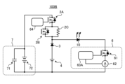
図13は、実施の形態3に係る発光素子駆動回路100Cの構成を示す回路図である。図13に示す実施の形態3に係る発光素子駆動回路100Cと、図1に示す実施の形態1に係る発光素子駆動回路100とを比較すると、図13では、補助電源である電源8Aと、MOSFET8Bと、ダイオード8Cとの直列回路が追加され、且つ、この直列回路の全体がダイオード3に並列に接続されている。発光素子駆動回路100Cにおいて、直列回路は、電圧加算手段として動作する。また、ダイオード8Cは、ダイオード3と同様に逆流防止素子として動作する。また、図13では、駆動部64Aが駆動部64に変更されている。なお、駆動部64は、駆動部64Aであってもよい。その他の構成は、図1の構成と同一又は同等であり、同一又は同等の構成要素には同一の符号を付して示すと共に、重複する説明は割愛する。なお、本稿では、MOSFET8Bを「第4のスイッチ素子」と記載することがある。
13 is a circuit diagram showing the configuration of a light-emitting element drive circuit 100C according to the third embodiment. Comparing the light-emitting element drive circuit 100C according to the third embodiment shown in FIG. 13 with the light-emitting element drive circuit 100 according to the first embodiment shown in FIG. 1, in FIG. 13, a series circuit of a power source 8A, which is an auxiliary power source, a MOSFET 8B, and a diode 8C is added, and the entire series circuit is connected in parallel to the diode 3. In the light-emitting element drive circuit 100C, the series circuit operates as a voltage adding means. Also, the diode 8C operates as a backflow prevention element like the diode 3. Also, in FIG. 13, the drive unit 64A is changed to the drive unit 64. The drive unit 64 may be the drive unit 64A. The other configurations are the same or equivalent to those in FIG. 1, and the same or equivalent components are denoted by the same reference numerals, and duplicated explanations are omitted. In this paper, the MOSFET 8B may be referred to as the "fourth switch element".
図13において、電源8Aの負極は主電圧源4の正極とダイオード3のアノードとの接続点に接続され、電源8Aの正極はMOSFET8Bのソースに接続されている。また、MOSFET8Bのドレインはダイオード8Cのアノードに接続され、ダイオード3のカソードとダイオード8Cのカソードとの接続点はLD10のアノードに接続されている。なお、図13では、ダイオード3のアノードとカソードとの間において、低電位側から高電位側に向かって、電源8A、MOSFET8B及びダイオード8Cの順で配置する構成を例示しているが、この構成に限定されない。直列回路を構成する各構成要素は、任意の2つ同士を互いに入れ替えてもよいし、3つの全てを入れ替えてもよい。
In FIG. 13, the negative electrode of power supply 8A is connected to the connection point between the positive electrode of main voltage source 4 and the anode of diode 3, and the positive electrode of power supply 8A is connected to the source of MOSFET 8B. The drain of MOSFET 8B is connected to the anode of diode 8C, and the connection point between the cathode of diode 3 and the cathode of diode 8C is connected to the anode of LD10. Note that FIG. 13 illustrates an example of a configuration in which power supply 8A, MOSFET 8B, and diode 8C are arranged in this order from the low potential side to the high potential side between the anode and cathode of diode 3, but this configuration is not limited to this. Any two of the components that make up the series circuit may be swapped with each other, or all three may be swapped.
図14は、実施の形態3に係る発光素子駆動回路100Cの動作説明に供するタイムチャートである。図14において、各波形は、上段側から、LD電流、印加電圧、MOSFET2Aの動作状態、MOSFET8Bの動作状態、及び電源8A電圧を表し、横軸は時間を表している。電源8A電圧は、電源8Aの出力電圧である。
FIG. 14 is a time chart explaining the operation of the light-emitting element drive circuit 100C according to the third embodiment. In FIG. 14, the waveforms represent, from the top, the LD current, the applied voltage, the operating state of MOSFET 2A, the operating state of MOSFET 8B, and the power supply 8A voltage, and the horizontal axis represents time. The power supply 8A voltage is the output voltage of the power supply 8A.
まず、MOSFET2Aがオンに制御されると、LD10のアノードに第1電圧が印加される。次に、MOSFET2Aがオフに制御される一方で、MOSFET8Bがオンに制御される。ここで、図14に示すタイムチャートは、MOSFET8Bがオンに制御された直後のLD10のアノードの電圧が第1電圧から変化しないように設定された動作を示している。具体的に、第1電圧、第2電圧及び電源8A開放電圧の間には、下記(1)式の関係がある。
First, when MOSFET 2A is controlled to be on, a first voltage is applied to the anode of LD10. Next, MOSFET 2A is controlled to be off, while MOSFET 8B is controlled to be on. Here, the time chart shown in FIG. 14 shows an operation set so that the voltage of the anode of LD10 immediately after MOSFET 8B is controlled to be on does not change from the first voltage. Specifically, the relationship between the first voltage, the second voltage, and the open voltage of the power supply 8A is expressed by the following formula (1).
(電源8A開放電圧)=(第1電圧)-(第2電圧) …(1)
(8A power supply open circuit voltage) = (first voltage) - (second voltage) ... (1)
電源8A開放電圧は、電源8Aに負荷が接続されないときの出力電圧である。なお、図14において、印加電圧の縦軸のスケールと、電源8A電圧の縦軸のスケールとは異なっていて、電源8A電圧は縦方向に拡大されて示されている。
The power supply 8A open circuit voltage is the output voltage when no load is connected to the power supply 8A. Note that in FIG. 14, the scale of the vertical axis of the applied voltage is different from the scale of the vertical axis of the power supply 8A voltage, and the power supply 8A voltage is shown expanded vertically.
電源8Aを介してLD電流が流れると、この電流により、電源8A電圧は、電源8Aにおける図示しない内部抵抗による電圧降下、MOSFET8Bのオン抵抗による電圧降下、及びダイオード8Cの順方向電圧降下を加算した分だけ低下していく。これにより、LD電流の供給がゆっくりと行われる。その後、印加電圧は、図14に示されるように、第2電圧に向かって徐々に減少していく。以上の動作により、LD電流の落ち込みを解消、もしくは小さくすることができる。
When the LD current flows through the power supply 8A, this current causes the power supply 8A voltage to drop by the sum of the voltage drop due to internal resistance (not shown) in the power supply 8A, the voltage drop due to the on-resistance of MOSFET 8B, and the forward voltage drop of diode 8C. This allows the LD current to be supplied slowly. After that, the applied voltage gradually decreases toward the second voltage, as shown in Figure 14. The above operation can eliminate or reduce the drop in the LD current.
電源8Aからの出力は、図7に示すような電流の落ち込み分のみを補償できればよい。このため、電源8Aは、低容量の電源でよい。但し、MOSFET2Aがオフに制御され、且つMOSFET8Bがオンに制御された直後の印加電圧の変化を小さくするため、電源8A電圧は、上記(1)式のように設定されていることが好ましい。上記(1)式のように設定されていれば、第1電圧から第2電圧への切り替え直後での電圧跳躍を抑えることができる。
The output from power supply 8A only needs to compensate for the current drop as shown in FIG. 7. For this reason, power supply 8A may be a low-capacity power supply. However, in order to reduce the change in applied voltage immediately after MOSFET 2A is controlled to be turned off and MOSFET 8B is controlled to be turned on, it is preferable that the power supply 8A voltage is set as shown in formula (1) above. If it is set as shown in formula (1) above, it is possible to suppress the voltage jump immediately after switching from the first voltage to the second voltage.
また、MOSFET8Bがオフに制御された直後の印加電圧の変化を小さくするため、電源8A電圧は、下記(2)式のように設定されていることが好ましい。下記(2)式のように設定されていれば、第1電圧から第2電圧への切り替え完了時における電圧跳躍を抑えることができる。
Furthermore, in order to reduce the change in applied voltage immediately after MOSFET 8B is controlled to be turned off, it is preferable that the power supply 8A voltage is set as shown in the following formula (2). If it is set as shown in the following formula (2), it is possible to suppress the voltage jump when switching from the first voltage to the second voltage is completed.
(電源8A切替完了電圧)
=(電源8A開放電圧)-(電源8A内部抵抗電圧降下)
-(MOSFET8Bオン抵抗電圧降下)-(ダイオード8C順方向電圧降下)
=(第2電圧) …(2) (Power supply 8A switching completion voltage)
= (Power supply 8A open circuit voltage) - (Power supply 8A internal resistance voltage drop)
- (MOSFET 8B on-resistance voltage drop) - (Diode 8C forward voltage drop)
= (second voltage) ... (2)
=(電源8A開放電圧)-(電源8A内部抵抗電圧降下)
-(MOSFET8Bオン抵抗電圧降下)-(ダイオード8C順方向電圧降下)
=(第2電圧) …(2) (
= (
- (
= (second voltage) ... (2)
図15は、実施の形態3の第1の変形例に係る発光素子駆動回路100Dの構成を示す回路図である。図13の構成において、電源8A自身が電源オン又は電源オフの機能を有している場合には、図15のように、電源8Aとダイオード8Cとの間に配置されていたMOSFET8Bを省略して構成することも可能である。
FIG. 15 is a circuit diagram showing the configuration of a light-emitting element driving circuit 100D according to a first modified example of the third embodiment. In the configuration of FIG. 13, if the power supply 8A itself has a function of turning the power supply on or off, it is also possible to omit the MOSFET 8B arranged between the power supply 8A and the diode 8C as shown in FIG. 15.
図16は、実施の形態3の第2の変形例に係る発光素子駆動回路100Eの構成を示す回路図である。図16に示す発光素子駆動回路100Eと、図1に示す実施の形態1に係る発光素子駆動回路100とを比較すると、図16では、抵抗8Eとダイオード8Fとによる並列回路がコンデンサ8Dと直列に接続された並列直列回路が追加され、且つ、この並列直列回路の全体がダイオード3に並列に接続されている。発光素子駆動回路100Eにおいて、並列直列回路は、電圧加算手段として動作する。また、コンデンサ8Dは、補助電源として動作する。また、図16では、駆動部64Aが駆動部64に変更されている。なお、駆動部64は、駆動部64Aであってもよい。その他の構成は、図1の構成と同一又は同等であり、同一又は同等の構成要素には同一の符号を付して示すと共に、重複する説明は割愛する。
16 is a circuit diagram showing the configuration of a light-emitting element driving circuit 100E according to a second modification of the third embodiment. Comparing the light-emitting element driving circuit 100E shown in FIG. 16 with the light-emitting element driving circuit 100 according to the first embodiment shown in FIG. 1, a parallel-series circuit is added in FIG. 16 in which a parallel circuit made of a resistor 8E and a diode 8F is connected in series with a capacitor 8D, and the entire parallel-series circuit is connected in parallel to a diode 3. In the light-emitting element driving circuit 100E, the parallel-series circuit operates as a voltage adding means. The capacitor 8D operates as an auxiliary power source. In FIG. 16, the driving unit 64A is changed to the driving unit 64. The driving unit 64 may be the driving unit 64A. The other configurations are the same or equivalent to those in FIG. 1, and the same or equivalent components are denoted by the same reference numerals, and duplicated explanations are omitted.
図17は、実施の形態3に係る発光素子駆動回路100Eの動作説明に供するタイムチャートである。図17において、各波形は、上段側から、LD電流、印加電圧、MOSFET2Aの動作状態及びコンデンサ8D電圧を表し、横軸は時間を表している。コンデンサ8D電圧は、コンデンサ8Dの両端電圧である。
FIG. 17 is a time chart explaining the operation of the light-emitting element drive circuit 100E according to the third embodiment. In FIG. 17, the waveforms represent, from the top, the LD current, the applied voltage, the operating state of the MOSFET 2A, and the capacitor 8D voltage, and the horizontal axis represents time. The capacitor 8D voltage is the voltage across the capacitor 8D.
MOSFET2Aがオンに制御されると、ブースト電圧源7からLD10に第1電圧が印加される。コンデンサ8Dは、第1電圧の印加時においては、この第1電圧と主電圧源4の出力電圧との差分電圧に充電される。コンデンサ8Dの充電電流は、電流制限抵抗である抵抗8Eによって制限される。これにより、高電圧である第1電圧によって、コンデンサ8Dに過大な突入電流が流れるのを防止できる。
When MOSFET 2A is controlled to be turned on, a first voltage is applied from boost voltage source 7 to LD 10. When the first voltage is applied, capacitor 8D is charged to the difference voltage between this first voltage and the output voltage of main voltage source 4. The charging current of capacitor 8D is limited by resistor 8E, which is a current limiting resistor. This makes it possible to prevent an excessive inrush current from flowing through capacitor 8D due to the high first voltage.
また、MOSFET2Aがオフに制御されると、コンデンサ8D電圧は、主電圧源4が出力する電圧に加算されてLD10のアノードに印加される。抵抗8Eの両端には、ダイオード8Fが接続されているので、コンデンサ8Dに蓄積された電荷の放電経路は、ダイオード8Fを通る経路となる。これにより、LD10への電力供給は、効率的に行われる。
Also, when MOSFET 2A is controlled to be turned off, the voltage of capacitor 8D is added to the voltage output by main voltage source 4 and applied to the anode of LD 10. Since diode 8F is connected across resistor 8E, the discharge path for the charge stored in capacitor 8D is the path through diode 8F. This allows power to be supplied to LD 10 efficiently.
回路動作は異なるが、第1電圧から第2電圧への切り替え直後における電圧跳躍、及び第1電圧から第2電圧への切り替え完了時における電圧跳躍の抑制は、図14のタイムチャートを使用して説明した方法と同様な方法で抑制することができる。具体的には、コンデンサ8Dの容量値、抵抗8Eの抵抗値、ダイオード8Fの順方向電圧特性などがパラメータになるが、これらのパラメータを適切に設定すれば、LD電流の落ち込みを解消、もしくは小さくすることができる。
Although the circuit operation is different, the voltage jump immediately after switching from the first voltage to the second voltage and the voltage jump when switching from the first voltage to the second voltage is completed can be suppressed in a manner similar to that described using the time chart in Figure 14. Specifically, the parameters are the capacitance value of capacitor 8D, the resistance value of resistor 8E, and the forward voltage characteristics of diode 8F, and by setting these parameters appropriately, the drop in LD current can be eliminated or reduced.
以上説明したように、実施の形態3に係る発光素子駆動回路は、補助電源と、第4のスイッチ素子と、ダイオードとの直列回路で構成され、この直列回路が逆流防止素子の両端に並列に接続される電圧加算手段を更に備える。電圧加算手段は、発光素子への印加電圧が第1電圧から第2電圧へ切り替わるときに、補助電源の電圧を第2の直流電源の出力電圧に加算するように動作する。これにより、第1の直流電源からの電流供給がゆっくりと遮断され、第2の直流電源による発光素子への電流供給が間に合うようになる。その結果、第2電圧の印加直後に起こり得る発光素子電流の落ち込みを解消、もしくは小さくすることができる。従って、実施の形態3に係る発光素子駆動回路は、実施の形態1の効果であるLD電流の立ち上がりの高速化と制御の安定性との両立を図りつつ、更に定電流駆動時の電流安定性を確保することが可能となる。
As described above, the light-emitting element drive circuit according to the third embodiment is composed of a series circuit of an auxiliary power supply, a fourth switch element, and a diode, and further includes a voltage adder means in which the series circuit is connected in parallel to both ends of the backflow prevention element. The voltage adder means operates to add the voltage of the auxiliary power supply to the output voltage of the second DC power supply when the voltage applied to the light-emitting element switches from the first voltage to the second voltage. This allows the current supply from the first DC power supply to be cut off slowly, and the current supply from the second DC power supply to the light-emitting element to be in time. As a result, it is possible to eliminate or reduce the drop in the light-emitting element current that may occur immediately after the application of the second voltage. Therefore, the light-emitting element drive circuit according to the third embodiment can ensure current stability during constant current drive while achieving both the effects of the first embodiment, namely, faster rise of the LD current and stable control.
なお、実施の形態3に係る発光素子駆動回路において、補助電源自身が電源オン又は電源オフの動作が可能な電源である場合、第4のスイッチ素子は省略可能である。
In the light-emitting element drive circuit according to embodiment 3, if the auxiliary power supply itself is a power supply that can be turned on or off, the fourth switch element can be omitted.
実施の形態3に係る発光素子駆動回路において、電圧加算手段は、抵抗と、ダイオードとによる並列回路がコンデンサと直列に接続された並列直列回路で構成されていてもよい。この構成において、コンデンサは、第1電圧の印加時においては、第1電圧と第2の直流電源の出力電圧との差分電圧によって充電され、第1電圧から第2電圧への切り替え時においては、電圧加算手段の補助電源として動作する。このような動作により、上述した電圧加算手段による作用効果を得ることが可能となる。
In the light-emitting element drive circuit according to the third embodiment, the voltage adder may be configured as a parallel-series circuit in which a parallel circuit made of a resistor and a diode is connected in series with a capacitor. In this configuration, when the first voltage is applied, the capacitor is charged by the differential voltage between the first voltage and the output voltage of the second DC power supply, and when switching from the first voltage to the second voltage, the capacitor operates as an auxiliary power supply for the voltage adder. This operation makes it possible to obtain the effect of the voltage adder described above.
実施の形態4.
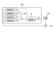
図18は、実施の形態4に係る発光素子駆動回路100Fの構成を示す回路図である。発光素子駆動回路100Fでは、大電流を流すアプリケーションに適用するため、図1のリニアレギュレータ6に相当する部分が並列化されて構成されている。図18に示す実施の形態4に係る発光素子駆動回路100Fと、図1に示す実施の形態1に係る発光素子駆動回路100とを比較すると、図18では、1つのMOSFET61が3つのMOSFET61B,61C,61Dに置き替えられ、1つの電流検出器62が3つの電流検出器62B,62C,62Dに置き替えられ、1つの駆動部63が3つの駆動部63B,63C,63Dに置き替えられている。また、図18では、駆動部64Aが駆動部64に変更されている。なお、駆動部64は、駆動部64Aであってもよい。その他の構成は、図1の構成と同一又は同等であり、同一又は同等の構成要素には同一の符号を付して示すと共に、重複する説明は割愛する。Embodiment 4.
FIG. 18 is a circuit diagram showing a configuration of a light-emittingelement drive circuit 100F according to a fourth embodiment. In the light-emitting element drive circuit 100F, a portion corresponding to the linear regulator 6 in FIG. 1 is configured in parallel in order to be applied to an application in which a large current flows. When comparing the light-emitting element drive circuit 100F according to the fourth embodiment shown in FIG. 18 with the light-emitting element drive circuit 100 according to the first embodiment shown in FIG. 1, in FIG. 18, one MOSFET 61 is replaced with three MOSFETs 61B, 61C, and 61D, one current detector 62 is replaced with three current detectors 62B, 62C, and 62D, and one drive unit 63 is replaced with three drive units 63B, 63C, and 63D. In addition, in FIG. 18, the drive unit 64A is changed to the drive unit 64. The drive unit 64 may be the drive unit 64A. The other configurations are the same or equivalent to those in FIG. 1, and the same or equivalent components are denoted by the same reference numerals, and duplicated explanations are omitted.
図18は、実施の形態4に係る発光素子駆動回路100Fの構成を示す回路図である。発光素子駆動回路100Fでは、大電流を流すアプリケーションに適用するため、図1のリニアレギュレータ6に相当する部分が並列化されて構成されている。図18に示す実施の形態4に係る発光素子駆動回路100Fと、図1に示す実施の形態1に係る発光素子駆動回路100とを比較すると、図18では、1つのMOSFET61が3つのMOSFET61B,61C,61Dに置き替えられ、1つの電流検出器62が3つの電流検出器62B,62C,62Dに置き替えられ、1つの駆動部63が3つの駆動部63B,63C,63Dに置き替えられている。また、図18では、駆動部64Aが駆動部64に変更されている。なお、駆動部64は、駆動部64Aであってもよい。その他の構成は、図1の構成と同一又は同等であり、同一又は同等の構成要素には同一の符号を付して示すと共に、重複する説明は割愛する。
FIG. 18 is a circuit diagram showing a configuration of a light-emitting
LD又はLEDのようなダイオード負荷は、ダイオード負荷に流れる電流によって、順方向電圧降下の大きさが変化する。このため図18の構成において、LD10と直列に接続されているMOSFET61B,61C,61Dの動作を最適化するには、MOSFET61B,61C,61Dに印加する第2電圧を調整する必要がある。これに伴い、図3に示す定数回路1又は2も、調整された第2電圧に適応した定数回路とする必要がある。
The magnitude of the forward voltage drop of a diode load such as an LD or LED changes depending on the current flowing through the diode load. For this reason, in the configuration of FIG. 18, in order to optimize the operation of MOSFETs 61B, 61C, and 61D connected in series with LD 10, it is necessary to adjust the second voltage applied to MOSFETs 61B, 61C, and 61D. Accordingly, constant circuit 1 or 2 shown in FIG. 3 must also be a constant circuit adapted to the adjusted second voltage.
図19は、図18に示す駆動部63Bの構成例を示す回路図であり、図20は、図18に示す駆動部63Cの構成例を示す回路図であり、図21は、図18に示す駆動部63Dの構成例を示す回路図である。
FIG. 19 is a circuit diagram showing an example of the configuration of the drive unit 63B shown in FIG. 18, FIG. 20 is a circuit diagram showing an example of the configuration of the drive unit 63C shown in FIG. 18, and FIG. 21 is a circuit diagram showing an example of the configuration of the drive unit 63D shown in FIG. 18.
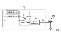
実施の形態1では、LD電流の立ち上がりの高速化と制御の安定性とを両立化するため、2つの定数回路を切り替えることについて説明した。LD電流が大きく異なれば、それに合わせた定数回路を備えていることが好ましい実施の形態となる。図19~21は、LD電流が大電流である場合と小電流である場合との2つに区分し、それに合わせて1つの駆動部が4つの定数回路を切り替える例としたものである。
In the first embodiment, we have described switching between two constant circuits to achieve both faster LD current rise and stable control. If the LD current differs significantly, a preferred embodiment would be one that has a constant circuit that matches the difference. Figures 19 to 21 show an example in which the LD current is divided into two cases, large and small, and one driver switches between four constant circuits accordingly.
具体的に、図19に示す駆動部63Bでは、4つの定数回路1-1,2-1,3-1,4-1がスイッチ機構SW1-1によって切り替えられる構成とされ、図20に示す駆動部63Cでは、4つの定数回路1-2,2-2,3-2,4-2がスイッチ機構SW1-2によって切り替えられる構成とされ、図21に示す駆動部63Dでは、4つの定数回路1-3,2-3,3-3,4-3がスイッチ機構SW1-3によって切り替えられる構成とされている。
Specifically, in the drive unit 63B shown in FIG. 19, four constant circuits 1-1, 2-1, 3-1, and 4-1 are configured to be switched by a switch mechanism SW1-1, in the drive unit 63C shown in FIG. 20, four constant circuits 1-2, 2-2, 3-2, and 4-2 are configured to be switched by a switch mechanism SW1-2, and in the drive unit 63D shown in FIG. 21, four constant circuits 1-3, 2-3, 3-3, and 4-3 are configured to be switched by a switch mechanism SW1-3.
図22は、図18の駆動部63B,63C,63Dを使用して制御した場合の動作説明に供する第1のタイムチャートである。図22において、上段側には、MOSFET61B,61C,61Dに流れるドレイン電流の波形が示され、下段側には、駆動部63B,63C,63Dに設定される制御定数が示されている。また、横軸は時間を表している。
FIG. 22 is a first time chart used to explain the operation when control is performed using the drivers 63B, 63C, and 63D of FIG. 18. In FIG. 22, the upper part shows the waveforms of the drain currents flowing through MOSFETs 61B, 61C, and 61D, and the lower part shows the control constants set in the drivers 63B, 63C, and 63D. The horizontal axis also represents time.
図22の例は、LD10には90[A]を流し、この90[A]の電流を3つのMOSFET61B,61C,61Dが均等に負担する例である。90[A]は大電流の一例である。また、MOSFET61B,61C,61Dに流せる最大電流を30[A]とする。
In the example of FIG. 22, 90 [A] flows through LD 10, and this 90 [A] current is shared equally by three MOSFETs 61B, 61C, and 61D. 90 [A] is an example of a large current. Also, the maximum current that can flow through MOSFETs 61B, 61C, and 61D is 30 [A].
図22に示されるように、駆動部63Bは、ドレイン電流が設定された30[A]になると、定数回路を定数回路1-1から定数回路2-1に切り替える。同様に、駆動部63Cは、ドレイン電流が30[A]になると、定数回路を定数回路1-2から定数回路2-2に切り替え、駆動部63Dは、ドレイン電流が30[A]になると、定数回路を定数回路1-3から定数回路2-3に切り替える。これらの動作により、LD電流を発振させずに、LD10を安定駆動することができる。
As shown in FIG. 22, when the drain current reaches the set value of 30 A, the driver 63B switches the constant circuit from constant circuit 1-1 to constant circuit 2-1. Similarly, when the drain current reaches 30 A, the driver 63C switches the constant circuit from constant circuit 1-2 to constant circuit 2-2, and when the drain current reaches 30 A, the driver 63D switches the constant circuit from constant circuit 1-3 to constant circuit 2-3. These operations enable stable operation of the LD 10 without oscillating the LD current.
図23は、図18の駆動部63B,63C,63Dを使用して制御した場合の動作説明に供する第2のタイムチャートである。波形の種類及び表記の仕方は、図22と同一である。
FIG. 23 is a second time chart used to explain the operation when controlled using the driving units 63B, 63C, and 63D in FIG. 18. The types of waveforms and the notation are the same as those in FIG. 22.
図23の例は、LD10には30[A]を流し、この30[A]の電流を3つのMOSFET61B,61C,61Dが均等に負担する例である。30[A]は大電流の他の例である。
In the example of FIG. 23, 30 [A] flows through LD 10, and this current of 30 [A] is shared equally by three MOSFETs 61B, 61C, and 61D. 30 [A] is another example of a large current.
図23に示されるように、駆動部63Bは、ドレイン電流が設定された10[A]になると、定数回路を定数回路3-1から定数回路4-1に切り替える。同様に、駆動部63Cは、ドレイン電流が10[A]になると、定数回路を定数回路3-2から定数回路4-2に切り替え、駆動部63Dは、ドレイン電流が10[A]になると、定数回路を定数回路3-3から定数回路4-3に切り替える。これらの動作により、LD電流を発振させずに、LD10を安定駆動することができる。
As shown in FIG. 23, when the drain current reaches the set value of 10 A, the driver 63B switches the constant circuit from constant circuit 3-1 to constant circuit 4-1. Similarly, when the drain current reaches 10 A, the driver 63C switches the constant circuit from constant circuit 3-2 to constant circuit 4-2, and when the drain current reaches 10 A, the driver 63D switches the constant circuit from constant circuit 3-3 to constant circuit 4-3. These operations enable stable operation of the LD 10 without oscillating the LD current.
なお、LD10に30[A]を流す場合、全てのMOSFETを動作させずに1つのMOSFETのみを動作させることも可能である。図24は、図18のMOSFET61Bのみを使用してLD10に電流を流した場合の動作説明に供するタイムチャートである。波形の種類及び表記の仕方は、図22と同一である。図24のように、MOSFET61Bのみに電流を流す場合には、駆動部63C,63Dは動作を休止し、駆動部63Bは、ドレイン電流が30[A]になると、定数回路を定数回路1-1から定数回路2-1に切り替える。これにより、LD電流は発振せず、LD10は安定駆動される。
When passing 30 [A] through LD10, it is also possible to operate only one MOSFET without operating all the MOSFETs. Figure 24 is a time chart used to explain operation when current is passed through LD10 using only MOSFET 61B in Figure 18. The types of waveforms and notation are the same as in Figure 22. When current is passed only through MOSFET 61B as in Figure 24, drive units 63C and 63D cease operation, and when the drain current reaches 30 [A], drive unit 63B switches the constant circuit from constant circuit 1-1 to constant circuit 2-1. This prevents the LD current from oscillating, and LD10 is driven stably.
図25は、図18のMOSFET61Cのみを使用してLD10に電流を流した場合の動作説明に供するタイムチャートである。波形の種類及び表記の仕方は、図22と同一である。図25のように、MOSFET61Cのみに電流を流す場合には、駆動部63B,63Dは動作を休止し、駆動部63Cは、ドレイン電流が30[A]になると、定数回路を定数回路1-2から定数回路2-2に切り替える。これにより、LD電流は発振せず、LD10は安定駆動される。
FIG. 25 is a time chart explaining the operation when current is passed through LD 10 using only MOSFET 61C in FIG. 18. The types of waveforms and the way of notation are the same as in FIG. 22. When current is passed through MOSFET 61C only as in FIG. 25, drivers 63B and 63D cease operation, and driver 63C switches the constant circuit from constant circuit 1-2 to constant circuit 2-2 when the drain current reaches 30 A. This prevents the LD current from oscillating, and LD 10 is driven stably.
図26は、図18のMOSFET61Dのみを使用してLD10に電流を流した場合の動作説明に供するタイムチャートである。波形の種類及び表記の仕方は、図22と同一である。図26のように、MOSFET61Dのみに電流を流す場合には、駆動部63B,63Cは動作を休止し、駆動部63Dは、ドレイン電流が30[A]になると、定数回路を定数回路1-3から定数回路2-3に切り替える。これにより、LD電流は発振せず、LD10は安定駆動される。
FIG. 26 is a time chart explaining the operation when current is passed through LD 10 using only MOSFET 61D in FIG. 18. The types of waveforms and the way they are expressed are the same as in FIG. 22. When current is passed through only MOSFET 61D as in FIG. 26, drivers 63B and 63C cease operation, and when the drain current reaches 30A, driver 63D switches the constant circuit from constant circuit 1-3 to constant circuit 2-3. This prevents the LD current from oscillating, and LD 10 is driven stably.
なお、実施の形態4に係る発光素子駆動回路100Fを図22及び図23のように動作させる場合と、図24~26のように動作させる場合とで比較すると、後者の方が利点が多い。前者のように動作させる場合、図19~21に示すように、各駆動部には4つの定数回路が必要となる。これに対し、後者のように動作させる場合、各駆動部は2つの定数回路を有する構成でよい。具体的な構成例を図27~29に示す。図27は、図18に示す駆動部63Bの他の構成例を示す回路図であり、図28は、図18に示す駆動部63Cの他の構成例を示す回路図であり、図29は、図18に示す駆動部63Dの他の構成例を示す回路図である。図27では、図19において示されていた定数回路3-1,4-1が省略可能となり、図28では、図20において示されていた定数回路3-2,4-2が省略可能となり、図29では、図21において示されていた定数回路3-3,4-3が省略可能となる。従って、後者の場合、回路面積の縮小などの効果が得られる。
Note that, when comparing the operation of the light-emitting element driving circuit 100F according to embodiment 4 as shown in FIG. 22 and FIG. 23 with the operation as shown in FIG. 24 to FIG. 26, the latter has more advantages. When operating as the former, as shown in FIG. 19 to FIG. 21, each driving unit needs four constant circuits. On the other hand, when operating as the latter, each driving unit may have two constant circuits. Specific configuration examples are shown in FIG. 27 to FIG. 29. FIG. 27 is a circuit diagram showing another configuration example of the driving unit 63B shown in FIG. 18, FIG. 28 is a circuit diagram showing another configuration example of the driving unit 63C shown in FIG. 18, and FIG. 29 is a circuit diagram showing another configuration example of the driving unit 63D shown in FIG. 18. In FIG. 27, the constant circuits 3-1 and 4-1 shown in FIG. 19 can be omitted, in FIG. 28, the constant circuits 3-2 and 4-2 shown in FIG. 20 can be omitted, and in FIG. 29, the constant circuits 3-3 and 4-3 shown in FIG. 21 can be omitted. Therefore, in the latter case, effects such as a reduction in circuit area can be achieved.
なお、1つのMOSFETのみを動作させる場合、負担を均等化する着意が必要である。このためには、通電するMOSFETを定期又は非定期に入れ替えるなどしてMOSFETの使用頻度を平準化する必要がある。MOSFETの使用頻度を平準化する例としては、MOSFETの駆動時間をカウントしておくタイマ機能を設けたり、MOSFETに流れた電流の積算量をカウントしておく機能を設けたりすることなどが考えられる。
When only one MOSFET is operated, it is necessary to consider equalizing the load. To achieve this, it is necessary to average out the frequency of MOSFET usage by, for example, switching the MOSFET that is energized on a regular or irregular basis. Examples of how to average out the frequency of MOSFET usage include providing a timer function that counts the operating time of the MOSFET, or providing a function that counts the accumulated amount of current that has flowed through the MOSFET.
また、上記の例では、3つのMOSFET61B,61C,61Dに均等な電流を流すものとしているが、この例に限定されない。例えばMOSFET61Bに流せる最大電流を10[A]とし、MOSFET61Cに流せる最大電流を20[A]とし、MOSFET61Dに流せる最大電流を40[A]とした場合を考える。この場合、LD10には、10[A]刻みで、10~70[A]の電流を流すことが可能となる。LD10の負荷特性にもよると考えられるが、電流が10[A]異なった場合、その電流に応じた定数回路を有しておき、印加電圧の切替時に定数回路を切り替える必要性が生じることも考えられる。この場合、10~70[A]の7つの電流に対応するには、7×2=14の定数回路が必要とされる。これに対し、図18に示すような並列駆動の構成を利用すれば、MOSFETの数×2、即ち3×2=6の定数回路で実現することが可能となる。
In the above example, the three MOSFETs 61B, 61C, and 61D are assumed to pass equal currents, but this is not limiting. For example, consider a case where the maximum current that can be passed through MOSFET 61B is 10 [A], the maximum current that can be passed through MOSFET 61C is 20 [A], and the maximum current that can be passed through MOSFET 61D is 40 [A]. In this case, it is possible to pass a current of 10 to 70 [A] in increments of 10 [A] through LD 10. Although it is considered to depend on the load characteristics of LD 10, if the current differs by 10 [A], it may be necessary to have a constant circuit corresponding to that current and to switch the constant circuit when switching the applied voltage. In this case, 7 x 2 = 14 constant circuits are required to handle seven currents from 10 to 70 [A]. In contrast, if a parallel drive configuration such as that shown in FIG. 18 is used, it is possible to realize this with constant circuits equal to the number of MOSFETs x 2, that is, 3 x 2 = 6.
以上説明したように、実施の形態4に係る発光素子駆動回路は、実施の形態1から3に係る発光素子駆動回路の構成において、リニアレギュレータの数は2以上であり、2以上のリニアレギュレータにおける第2のスイッチ素子は、相互に並列に接続されている。2以上の第2のスイッチ素子は、同時には1つのみが駆動され、駆動される第2のスイッチ素子は、定期又は非定期に入れ替えられる。このようにすれば、2以上の第2のスイッチ素子間の使用頻度を平準化することが可能となる。
As described above, the light-emitting element drive circuit of embodiment 4 has the same configuration as the light-emitting element drive circuit of embodiments 1 to 3, but with two or more linear regulators, and the second switch elements in the two or more linear regulators are connected in parallel with each other. Only one of the two or more second switch elements is driven at a time, and the driven second switch elements are switched periodically or irregularly. In this way, it is possible to equalize the frequency of use between the two or more second switch elements.
また、上記の構成において、2以上の第2のスイッチ素子は、2以上が同時に駆動されるように構成されていてもよい。2つ以上が同時に駆動される場合、第2のスイッチ素子は、相互に異なる電流が流れるように駆動される。このような駆動を行えば、駆動電流値を小刻みに設定した場合であっても、定数回路の数が比例的に増加するのを回避することができる。これにより、駆動電流の設定値の数が増加した場合でも、回路面積の増加を抑制することが可能となる。
Furthermore, in the above configuration, the two or more second switch elements may be configured so that two or more are driven simultaneously. When two or more are driven simultaneously, the second switch elements are driven so that different currents flow through them. By driving in this manner, even if the drive current value is set in small increments, it is possible to avoid a proportional increase in the number of constant circuits. This makes it possible to suppress an increase in the circuit area even if the number of drive current setting values increases.
実施の形態5.
実施の形態5では、発光素子駆動において、上述した実施の形態1~4の制御を実現するためのより具体的な回路構成について説明する。図30は、実施の形態5に係る発光素子駆動回路100Gの構成を示す回路図である。図30では、図1に示す発光素子駆動回路100の構成において、制御部81が追加されている。その他の構成は、図1に示す発光素子駆動回路100と同一又は同等であり、同一又は同等の構成部には同一の符号を付し、重複する説明は割愛する。 Embodiment 5.
In the fifth embodiment, a more specific circuit configuration for realizing the control of the first to fourth embodiments described above in driving the light-emitting element will be described. Fig. 30 is a circuit diagram showing the configuration of a light-emittingelement drive circuit 100G according to the fifth embodiment. In Fig. 30, a control unit 81 is added to the configuration of the light-emitting element drive circuit 100 shown in Fig. 1. The other configurations are the same or equivalent to those of the light-emitting element drive circuit 100 shown in Fig. 1, and the same or equivalent components are denoted by the same reference numerals, and duplicated explanations will be omitted.
実施の形態5では、発光素子駆動において、上述した実施の形態1~4の制御を実現するためのより具体的な回路構成について説明する。図30は、実施の形態5に係る発光素子駆動回路100Gの構成を示す回路図である。図30では、図1に示す発光素子駆動回路100の構成において、制御部81が追加されている。その他の構成は、図1に示す発光素子駆動回路100と同一又は同等であり、同一又は同等の構成部には同一の符号を付し、重複する説明は割愛する。 Embodiment 5.
In the fifth embodiment, a more specific circuit configuration for realizing the control of the first to fourth embodiments described above in driving the light-emitting element will be described. Fig. 30 is a circuit diagram showing the configuration of a light-emitting
制御部81は、外部からの電流指令値と、電流検出器62の検出値に基づいて、駆動部63Aを制御するための制御信号を生成して、駆動部63Aに出力する。駆動部63Aは、制御部81から出力される制御信号に基づいて、MOSFET61の導通を制御する。
The control unit 81 generates a control signal for controlling the drive unit 63A based on an external current command value and the detection value of the current detector 62, and outputs the control signal to the drive unit 63A. The drive unit 63A controls the conduction of the MOSFET 61 based on the control signal output from the control unit 81.
具体的な信号について説明する。図31は、実施の形態5に係る制御部81と駆動部63Aとの間の接続関係を示す回路図である。なお、図31では、制御部81及び図6に示す駆動部63Aと共に、MOSFET61及び電流検出器62が示されている。
Specific signals will be described. FIG. 31 is a circuit diagram showing the connection relationship between the control unit 81 and the drive unit 63A according to embodiment 5. Note that FIG. 31 shows the MOSFET 61 and the current detector 62 together with the control unit 81 and the drive unit 63A shown in FIG. 6.
制御部81は、外部からの電流指令値と電流検出器62の検出値とに基づいて、駆動部63Aを制御するための制御信号を生成する。具体的に、制御部81は、定数回路1と定数回路2とを切り替えるスイッチ機構SW1への制御信号、MOSFET61を制御するためのゲート駆動回路68の制御信号を生成する。また、制御部81は、電流検出器62が検出した電流検出値を定数回路1,2へ出力する。電流検出値は、制御部81を通らずに、直接電流検出器62から定数回路1,2に対して直接的に送信される構成でもよい。電流検出値が制御部81を介して、定数回路1,2へ送信される構成の場合、制御部81でノイズ除去や信号のレベルシフト、増幅などを行うことができる。従って、この構成の場合、定数回路1,2及びその後段のゲート駆動回路68への過電圧防止を図ることができ、駆動部63Aに対する制御精度向上を図ることも可能となる。また、この構成の場合、電流検出値の検出値が過電流であったときには、その旨の信号をゲート駆動回路68へ送り、MOSFET61をOFFさせることができるので、LD10に過電流が流れるのを防止することが可能となる。
The control unit 81 generates a control signal for controlling the drive unit 63A based on a current command value from the outside and the detection value of the current detector 62. Specifically, the control unit 81 generates a control signal for the switch mechanism SW1 that switches between constant circuit 1 and constant circuit 2, and a control signal for the gate drive circuit 68 that controls the MOSFET 61. The control unit 81 also outputs the current detection value detected by the current detector 62 to the constant circuits 1 and 2. The current detection value may be directly transmitted from the current detector 62 to the constant circuits 1 and 2 without passing through the control unit 81. In the case where the current detection value is transmitted to the constant circuits 1 and 2 via the control unit 81, the control unit 81 can perform noise removal, signal level shifting, amplification, etc. Therefore, in this configuration, it is possible to prevent overvoltage to the constant circuits 1 and 2 and the gate drive circuit 68 in the subsequent stage, and it is also possible to improve the control accuracy for the drive unit 63A. In addition, in this configuration, if the current detection value indicates an overcurrent, a signal to that effect can be sent to the gate drive circuit 68 to turn off the MOSFET 61, making it possible to prevent an overcurrent from flowing through the LD 10.
制御部81の動作については、図7を用いて説明する。制御部81は、第2電圧の期間では、定数回路1を使用できるようにスイッチ機構SW1を制御して、MOSFET61をオンに制御する。LD10に流れる電流が目標値に達した場合には、定数回路2を使用できるようにスイッチ機構SW1を制御して、第1電圧に切り替える。このようにすれば、LD電流の落ち込みを、最小限にすることが可能となる。なお、定数回路2への切り替えは、LD10に流れる電流が目標値に達した直後である必要はなく、LD10に流れる電流が目標値に達してから、ある期間の経過後であってもよい。なお、電流の目標値は、電流指令値として外部から入力される。
The operation of the control unit 81 will be described with reference to FIG. 7. During the second voltage period, the control unit 81 controls the switch mechanism SW1 to turn on the MOSFET 61 so that the constant circuit 1 can be used. When the current flowing through LD 10 reaches the target value, the control unit 81 controls the switch mechanism SW1 to switch to the first voltage so that the constant circuit 2 can be used. In this way, it is possible to minimize the drop in the LD current. Note that the switch to the constant circuit 2 does not have to be immediately after the current flowing through LD 10 reaches the target value, but may be after a certain period has elapsed since the current flowing through LD 10 reaches the target value. Note that the target current value is input from outside as a current command value.
なお、実施の形態5では、制御部81を有する構成を図1に示す発光素子駆動回路100に適用する例を説明したが、この例に限定されない。制御部81については,発光素子駆動回路100A,100B,100C,100D,100E,及び100Fのそれぞれに適用することが可能である。
In the fifth embodiment, an example is described in which a configuration having a control unit 81 is applied to the light-emitting element drive circuit 100 shown in FIG. 1, but the present invention is not limited to this example. The control unit 81 can be applied to each of the light-emitting element drive circuits 100A, 100B, 100C, 100D, 100E, and 100F.
制御部81のハードウェア構成は、処理回路や信号の入出力を行うインタフェースを含む構成とすることができる。処理回路は、ノイズフィルター回路や信号増幅回路などを含め、単一回路、複合回路、ASIC(Application Specific Integrated Circuit)、FPGA(Field-Programmable Gate Array)、又は、これらを組み合わせたものが該当する。処理回路に入力する情報、及び処理回路から出力する情報は、インタフェースを介して入手することができる。また、本開示に係る制御部81の機能を実現する際に、より高度な演算処理を行う場合には、処理回路に代えて、演算を行うプロセッサと、プロセッサによって読みとられるプログラムが保存されるメモリとを備えるように構成してもよい。
The hardware configuration of the control unit 81 can include a processing circuit and an interface for inputting and outputting signals. The processing circuit can be a single circuit, a composite circuit, an ASIC (Application Specific Integrated Circuit), an FPGA (Field-Programmable Gate Array), or a combination of these, including a noise filter circuit and a signal amplifier circuit. Information input to the processing circuit and information output from the processing circuit can be obtained via an interface. In addition, when performing more advanced arithmetic processing to realize the functions of the control unit 81 according to the present disclosure, the control unit 81 may be configured to include a processor that performs arithmetic operations and a memory in which programs read by the processor are stored, instead of a processing circuit.
以上の実施の形態に示した構成は、一例を示すものであり、別の公知の技術と組み合わせることも可能であるし、実施の形態同士を組み合わせることも可能であるし、要旨を逸脱しない範囲で、構成の一部を省略、変更することも可能である。
The configurations shown in the above embodiments are merely examples, and may be combined with other known technologies, or the embodiments may be combined with each other. In addition, parts of the configurations may be omitted or modified without departing from the spirit of the invention.
1,1-1,1-2,1-3,2,2-1,2-2,2-3,3-1,3-2,3-3,4-1,4-2,4-3 定数回路、2A,2B,3A,8B,61,61B,61C,61D MOSFET、2C,8E 抵抗、3,8C,8F,D1,D2 ダイオード、4 主電圧源、6 リニアレギュレータ、7 ブースト電圧源、8A 電源、8D,71 コンデンサ、10 LD、62,62B,62C,62D 電流検出器、63A,63B,63C,63D 駆動部、64,64A 第2の駆動部、68,69 ゲート駆動回路、72 電圧源、81 制御部、100,100A,100B,100C,100D,100E,100F,100G 発光素子駆動回路、L1,L2,L3-1,L3-2,L3-3 配線インダクタンス、Rg,Rg1,Rgoff,Rgon ゲート抵抗、SW1,SW1-1,SW1-2,SW1-3 スイッチ機構。
1, 1-1, 1-2, 1-3, 2, 2-1, 2-2, 2-3, 3-1, 3-2, 3-3, 4-1, 4-2, 4-3 Constant circuit, 2A, 2B, 3A, 8B, 61, 61B, 61C, 61D MOSFET, 2C, 8E Resistor, 3, 8C, 8F, D1, D2 Diode, 4 Main voltage source, 6 Linear regulator, 7 Boost voltage source, 8A Power source, 8D, 71 Capacitor, 10 LD, 62, 62B, 62C, 62D Current detector , 63A, 63B, 63C, 63D Drive unit, 64, 64A Second drive unit, 68, 69 Gate drive circuit, 72 Voltage source, 81 Control unit, 100, 100A, 100B, 100C, 100D, 100E, 100F, 100G Light-emitting element drive circuit, L1, L2, L3-1, L3-2, L3-3 Wiring inductance, Rg, Rg1, Rgoff, Rgon Gate resistance, SW1, SW1-1, SW1-2, SW1-3 Switch mechanism.
Claims (15)
- 発光素子を駆動する発光素子駆動回路であって、
第1電圧を保持し、前記発光素子のアノードに前記第1電圧を印加可能に接続される第1の直流電源と、
前記発光素子のアノードに前記第1電圧よりも低い第2電圧を印加可能に接続される第2の直流電源と、
前記発光素子のアノードに対する前記第1電圧の印加のオンオフを切り替える第1のスイッチ素子と、
前記第1電圧が前記第2の直流電源へ印加されるのを防止する向きに接続される逆流防止素子と、
前記発光素子に流れる電流を制御するリニアレギュレータと、
を備え、
前記リニアレギュレータは、
前記発光素子に流れる電流を検出する電流検出器と、
前記発光素子に流れる電流が通流する第2のスイッチ素子と、
前記第2のスイッチ素子を駆動する駆動部と、
を備え、
前記駆動部は、
前記第2のスイッチ素子のゲートを駆動するゲート駆動回路と、
互いに異なる制御定数が設定される2以上の定数回路と、
前記発光素子への印加電圧が前記第1電圧であるか前記第2電圧であるかに応じて、前記2以上の定数回路のうちの1つを選択して前記ゲート駆動回路に接続するスイッチ機構と、
を備えたことを特徴とする発光素子駆動回路。 A light emitting element drive circuit for driving a light emitting element,
a first DC power supply that holds a first voltage and is connected to the anode of the light-emitting element so as to be able to apply the first voltage;
a second DC power source connected to the anode of the light emitting element so as to be capable of applying a second voltage lower than the first voltage;
a first switch element that switches on and off the application of the first voltage to the anode of the light-emitting element;
a backflow prevention element connected in a direction to prevent the first voltage from being applied to the second DC power supply;
a linear regulator for controlling a current flowing through the light emitting element;
Equipped with
The linear regulator comprises:
a current detector for detecting a current flowing through the light-emitting element;
a second switch element through which a current flows to the light emitting element;
a drive unit that drives the second switch element;
Equipped with
The drive unit is
a gate drive circuit that drives a gate of the second switch element;
Two or more constant circuits in which different control constants are set;
a switch mechanism that selects one of the two or more constant circuits and connects it to the gate drive circuit depending on whether a voltage applied to the light-emitting element is the first voltage or the second voltage;
A light emitting element drive circuit comprising: - 前記発光素子への印加電圧が前記第1電圧から前記第2電圧へ切り替わるときに前記印加電圧の変化を緩和する電圧変化緩和手段を更に備えたことを特徴とする請求項1に記載の発光素子駆動回路。 The light-emitting element drive circuit according to claim 1, further comprising a voltage change mitigation means for mitigating a change in the applied voltage when the applied voltage to the light-emitting element is switched from the first voltage to the second voltage.
- 前記第1のスイッチ素子を駆動する第2の駆動部を備え、
前記電圧変化緩和手段は、前記第2の駆動部に設けられる
ことを特徴とする請求項2に記載の発光素子駆動回路。 a second drive unit that drives the first switch element,
The light-emitting element drive circuit according to claim 2 , wherein the voltage change mitigation means is provided in the second drive section. - 前記第1のスイッチ素子は、プレーナー構造の金属酸化膜半導体電界効果型トランジスタである
ことを特徴とする請求項3に記載の発光素子駆動回路。 4. The light-emitting element drive circuit according to claim 3, wherein the first switch element is a metal oxide semiconductor field effect transistor having a planar structure. - 前記電圧変化緩和手段は、第3のスイッチ素子と、抵抗との並列回路で構成され、
前記並列回路は、前記発光素子及び前記逆流防止素子の接続点と前記第2のスイッチ素子との間、又は、前記第1の直流電源の正極と前記第2のスイッチ素子との間に配置される
ことを特徴とする請求項4に記載の発光素子駆動回路。 the voltage change mitigation means is configured with a parallel circuit of a third switch element and a resistor,
5. The light-emitting element drive circuit according to claim 4, wherein the parallel circuit is arranged between a connection point of the light-emitting element and the backflow prevention element and the second switch element, or between a positive electrode of the first DC power supply and the second switch element. - 前記第3のスイッチ素子は前記第1電圧の印加時にオンに制御され、前記第1電圧から前記第2電圧への切り替え時にオフに制御される
ことを特徴とする請求項5に記載の発光素子駆動回路。 6. The light-emitting element drive circuit according to claim 5, wherein the third switch element is controlled to be on when the first voltage is applied, and is controlled to be off when switching from the first voltage to the second voltage. - 補助電源を有し、前記発光素子への印加電圧が前記第1電圧から前記第2電圧へ切り替わるときに前記補助電源の電圧を前記第2の直流電源の出力電圧に加算する電圧加算手段を更に備えたことを特徴とする請求項1に記載の発光素子駆動回路。 The light-emitting element drive circuit according to claim 1, further comprising a voltage adding means for adding the voltage of the auxiliary power supply to the output voltage of the second DC power supply when the voltage applied to the light-emitting element is switched from the first voltage to the second voltage.
- 前記電圧加算手段は、前記補助電源と、第4のスイッチ素子と、ダイオードとの直列回路で構成され、
前記直列回路は、前記逆流防止素子の両端に並列に接続される
ことを特徴とする請求項7に記載の発光素子駆動回路。 the voltage adder means is configured with a series circuit of the auxiliary power supply, a fourth switch element, and a diode,
The light-emitting element drive circuit according to claim 7 , wherein the series circuit is connected in parallel to both ends of the backflow prevention element. - 前記電圧加算手段は、前記補助電源と、ダイオードとの直列回路で構成され、
前記補助電源は、電源オン又は電源オフの動作が可能な電源であり、
前記直列回路は、前記逆流防止素子の両端に並列に接続される
ことを特徴とする請求項7に記載の発光素子駆動回路。 the voltage adder means is configured with a series circuit of the auxiliary power supply and a diode,
The auxiliary power supply is a power supply that can be turned on or off,
The light-emitting element drive circuit according to claim 7 , wherein the series circuit is connected in parallel to both ends of the backflow prevention element. - 前記電圧加算手段は、抵抗と、ダイオードとによる並列回路がコンデンサと直列に接続された並列直列回路で構成され、
前記並列直列回路は、前記逆流防止素子の両端に並列に接続される
ことを特徴とする請求項7に記載の発光素子駆動回路。 the voltage adding means is configured with a parallel-series circuit in which a parallel circuit made of a resistor and a diode is connected in series with a capacitor,
The light-emitting element drive circuit according to claim 7 , wherein the parallel-series circuit is connected in parallel to both ends of the backflow prevention element. - 前記コンデンサは、
前記第1電圧の印加時においては、前記第1電圧と前記第2の直流電源の出力電圧との差分電圧によって充電され、
前記第1電圧から前記第2電圧への切り替え時においては、前記電圧加算手段の前記補助電源として動作する
ことを特徴とする請求項10に記載の発光素子駆動回路。 The capacitor is
When the first voltage is applied, the capacitor is charged by a difference voltage between the first voltage and an output voltage of the second DC power supply,
11. The light-emitting element drive circuit according to claim 10, wherein the light-emitting element drive circuit operates as the auxiliary power supply for the voltage adder when the first voltage is switched to the second voltage. - 前記リニアレギュレータの数は2以上であり、
2以上の前記リニアレギュレータにおける前記第2のスイッチ素子は、相互に並列に接続されている
ことを特徴とする請求項1から11の何れか1項に記載の発光素子駆動回路。 the number of the linear regulators is two or more;
12. The light-emitting element drive circuit according to claim 1, wherein the second switch elements in two or more of the linear regulators are connected in parallel with each other. - 2以上の前記第2のスイッチ素子は、同時には1つのみが駆動され、駆動される前記第2のスイッチ素子は、定期又は非定期に入れ替えられる
ことを特徴とする請求項12に記載の発光素子駆動回路。 13. The light-emitting element drive circuit according to claim 12, wherein only one of the two or more second switch elements is driven at a time, and the driven second switch elements are switched periodically or non-periodically. - 2以上の前記第2のスイッチ素子は、1つ以上が同時に駆動され、2つ以上が同時に駆動される場合、駆動される前記第2のスイッチ素子には、相互に異なる電流が流れる
ことを特徴とする請求項12に記載の発光素子駆動回路。 The light-emitting element drive circuit according to claim 12, characterized in that one or more of the two or more second switch elements are driven simultaneously, and when two or more are driven simultaneously, different currents flow through the driven second switch elements. - 外部からの電流指令値と、前記電流検出器の検出値とに基づいて、前記駆動部を制御するための制御信号を生成する制御部を備えたことを特徴とする請求項1から14の何れか1項に記載の発光素子駆動回路。 The light-emitting element drive circuit according to any one of claims 1 to 14, further comprising a control unit that generates a control signal for controlling the drive unit based on a current command value from an external source and a detection value of the current detector.
Applications Claiming Priority (2)
| Application Number | Priority Date | Filing Date | Title |
|---|---|---|---|
| JP2022-155285 | 2022-09-28 | ||
| JP2022155285 | 2022-09-28 |
Publications (1)
| Publication Number | Publication Date |
|---|---|
| WO2024070709A1 true WO2024070709A1 (en) | 2024-04-04 |
Family
ID=90477431
Family Applications (1)
| Application Number | Title | Priority Date | Filing Date |
|---|---|---|---|
| PCT/JP2023/033414 WO2024070709A1 (en) | 2022-09-28 | 2023-09-13 | Light emitting element drive circuit |
Country Status (1)
| Country | Link |
|---|---|
| WO (1) | WO2024070709A1 (en) |
Citations (2)
| Publication number | Priority date | Publication date | Assignee | Title |
|---|---|---|---|---|
| JP2000307186A (en) * | 1999-04-22 | 2000-11-02 | Ricoh Co Ltd | Image forming device |
| JP2002335038A (en) * | 2001-03-05 | 2002-11-22 | Fuji Xerox Co Ltd | Light emitting element driver and light emitting device driving system |
-
2023
- 2023-09-13 WO PCT/JP2023/033414 patent/WO2024070709A1/en unknown
Patent Citations (2)
| Publication number | Priority date | Publication date | Assignee | Title |
|---|---|---|---|---|
| JP2000307186A (en) * | 1999-04-22 | 2000-11-02 | Ricoh Co Ltd | Image forming device |
| JP2002335038A (en) * | 2001-03-05 | 2002-11-22 | Fuji Xerox Co Ltd | Light emitting element driver and light emitting device driving system |
Similar Documents
| Publication | Publication Date | Title |
|---|---|---|
| KR101679629B1 (en) | Electronic circuits and methods for driving a light emitting diode (led) load | |
| US9350241B2 (en) | Buck converter and control method therefor | |
| JP4317825B2 (en) | Inverter device | |
| JP7268507B2 (en) | Gate drive and power converter | |
| US8390212B2 (en) | Light-emitting element driving control circuit | |
| KR20130135775A (en) | Lighting device and vehicle headlamp | |
| JP2008541507A (en) | Power field effect transistor (FET) drive system and method | |
| KR20090006013A (en) | Solenoid valve driving circuit and solenoid valve | |
| KR20110123169A (en) | Switching gate drive | |
| US8829836B2 (en) | Driver for switching element and control system for rotary machine using the same | |
| JP2018206848A (en) | Drive circuit and light-emitting device | |
| JP2010063332A (en) | Load driving device | |
| US10483853B2 (en) | DC-DC converter | |
| JP6656186B2 (en) | Regenerative current detection circuit, charge current detection circuit, motor current detection system | |
| US9603227B2 (en) | Semiconductor light source driving apparatus | |
| WO2024070709A1 (en) | Light emitting element drive circuit | |
| JP2013187528A (en) | Light-emitting element drive | |
| EP2391184A2 (en) | Led driver circuit | |
| KR102192393B1 (en) | Led system for vehicle lighting having high efficiency and high reliability | |
| JP2014078421A (en) | Light emitting diode activation device an illuminating device using the light emitting diode activation device | |
| WO2020202967A1 (en) | In-vehicle voltage conversion device | |
| CN114244339B (en) | Gate drive circuit and electronic device | |
| KR102261852B1 (en) | Ac direct led driver including capacitor for led driver | |
| JP7094910B2 (en) | Stepping motor control device, stepping motor control method and stepping motor drive control system | |
| US20210273404A1 (en) | Laser drive circuit and sensor apparatus |