WO2024048762A1 - 半導体パッケージを製造する方法 - Google Patents
半導体パッケージを製造する方法 Download PDFInfo
- Publication number
- WO2024048762A1 WO2024048762A1 PCT/JP2023/032012 JP2023032012W WO2024048762A1 WO 2024048762 A1 WO2024048762 A1 WO 2024048762A1 JP 2023032012 W JP2023032012 W JP 2023032012W WO 2024048762 A1 WO2024048762 A1 WO 2024048762A1
- Authority
- WO
- WIPO (PCT)
- Prior art keywords
- layer
- internal
- resin layer
- wiring
- trench
- Prior art date
- Legal status (The legal status is an assumption and is not a legal conclusion. Google has not performed a legal analysis and makes no representation as to the accuracy of the status listed.)
- Ceased
Links
Images










Classifications
-
- H—ELECTRICITY
- H10—SEMICONDUCTOR DEVICES; ELECTRIC SOLID-STATE DEVICES NOT OTHERWISE PROVIDED FOR
- H10W—GENERIC PACKAGES, INTERCONNECTIONS, CONNECTORS OR OTHER CONSTRUCTIONAL DETAILS OF DEVICES COVERED BY CLASS H10
- H10W70/00—Package substrates; Interposers; Redistribution layers [RDL]
- H10W70/01—Manufacture or treatment
- H10W70/05—Manufacture or treatment of insulating or insulated package substrates, or of interposers, or of redistribution layers
-
- H—ELECTRICITY
- H10—SEMICONDUCTOR DEVICES; ELECTRIC SOLID-STATE DEVICES NOT OTHERWISE PROVIDED FOR
- H10W—GENERIC PACKAGES, INTERCONNECTIONS, CONNECTORS OR OTHER CONSTRUCTIONAL DETAILS OF DEVICES COVERED BY CLASS H10
- H10W20/00—Interconnections in chips, wafers or substrates
- H10W20/40—Interconnections external to wafers or substrates, e.g. back-end-of-line [BEOL] metallisations or vias connecting to gate electrodes
- H10W20/41—Interconnections external to wafers or substrates, e.g. back-end-of-line [BEOL] metallisations or vias connecting to gate electrodes characterised by their conductive parts
- H10W20/43—Layouts of interconnections
-
- H—ELECTRICITY
- H05—ELECTRIC TECHNIQUES NOT OTHERWISE PROVIDED FOR
- H05K—PRINTED CIRCUITS; CASINGS OR CONSTRUCTIONAL DETAILS OF ELECTRIC APPARATUS; MANUFACTURE OF ASSEMBLAGES OF ELECTRICAL COMPONENTS
- H05K1/00—Printed circuits
- H05K1/02—Details
-
- H—ELECTRICITY
- H05—ELECTRIC TECHNIQUES NOT OTHERWISE PROVIDED FOR
- H05K—PRINTED CIRCUITS; CASINGS OR CONSTRUCTIONAL DETAILS OF ELECTRIC APPARATUS; MANUFACTURE OF ASSEMBLAGES OF ELECTRICAL COMPONENTS
- H05K3/00—Apparatus or processes for manufacturing printed circuits
-
- H—ELECTRICITY
- H05—ELECTRIC TECHNIQUES NOT OTHERWISE PROVIDED FOR
- H05K—PRINTED CIRCUITS; CASINGS OR CONSTRUCTIONAL DETAILS OF ELECTRIC APPARATUS; MANUFACTURE OF ASSEMBLAGES OF ELECTRICAL COMPONENTS
- H05K3/00—Apparatus or processes for manufacturing printed circuits
- H05K3/0011—Working of insulating substrates or insulating layers
- H05K3/0044—Mechanical working of the substrate, e.g. drilling or punching
-
- H—ELECTRICITY
- H05—ELECTRIC TECHNIQUES NOT OTHERWISE PROVIDED FOR
- H05K—PRINTED CIRCUITS; CASINGS OR CONSTRUCTIONAL DETAILS OF ELECTRIC APPARATUS; MANUFACTURE OF ASSEMBLAGES OF ELECTRICAL COMPONENTS
- H05K3/00—Apparatus or processes for manufacturing printed circuits
- H05K3/10—Apparatus or processes for manufacturing printed circuits in which conductive material is applied to the insulating support in such a manner as to form the desired conductive pattern
- H05K3/20—Apparatus or processes for manufacturing printed circuits in which conductive material is applied to the insulating support in such a manner as to form the desired conductive pattern by affixing prefabricated conductor pattern
-
- H—ELECTRICITY
- H05—ELECTRIC TECHNIQUES NOT OTHERWISE PROVIDED FOR
- H05K—PRINTED CIRCUITS; CASINGS OR CONSTRUCTIONAL DETAILS OF ELECTRIC APPARATUS; MANUFACTURE OF ASSEMBLAGES OF ELECTRICAL COMPONENTS
- H05K3/00—Apparatus or processes for manufacturing printed circuits
- H05K3/22—Secondary treatment of printed circuits
- H05K3/28—Applying non-metallic protective coatings
-
- H—ELECTRICITY
- H05—ELECTRIC TECHNIQUES NOT OTHERWISE PROVIDED FOR
- H05K—PRINTED CIRCUITS; CASINGS OR CONSTRUCTIONAL DETAILS OF ELECTRIC APPARATUS; MANUFACTURE OF ASSEMBLAGES OF ELECTRICAL COMPONENTS
- H05K3/00—Apparatus or processes for manufacturing printed circuits
- H05K3/30—Assembling printed circuits with electric components, e.g. with resistors
- H05K3/303—Assembling printed circuits with electric components, e.g. with resistors with surface mounted components
-
- H—ELECTRICITY
- H05—ELECTRIC TECHNIQUES NOT OTHERWISE PROVIDED FOR
- H05K—PRINTED CIRCUITS; CASINGS OR CONSTRUCTIONAL DETAILS OF ELECTRIC APPARATUS; MANUFACTURE OF ASSEMBLAGES OF ELECTRICAL COMPONENTS
- H05K3/00—Apparatus or processes for manufacturing printed circuits
- H05K3/46—Manufacturing multilayer circuits
-
- H—ELECTRICITY
- H05—ELECTRIC TECHNIQUES NOT OTHERWISE PROVIDED FOR
- H05K—PRINTED CIRCUITS; CASINGS OR CONSTRUCTIONAL DETAILS OF ELECTRIC APPARATUS; MANUFACTURE OF ASSEMBLAGES OF ELECTRICAL COMPONENTS
- H05K3/00—Apparatus or processes for manufacturing printed circuits
- H05K3/46—Manufacturing multilayer circuits
- H05K3/4644—Manufacturing multilayer circuits by building the multilayer layer by layer, i.e. build-up multilayer circuits
- H05K3/467—Adding a circuit layer by thin film methods
-
- H—ELECTRICITY
- H10—SEMICONDUCTOR DEVICES; ELECTRIC SOLID-STATE DEVICES NOT OTHERWISE PROVIDED FOR
- H10P—GENERIC PROCESSES OR APPARATUS FOR THE MANUFACTURE OR TREATMENT OF DEVICES COVERED BY CLASS H10
- H10P72/00—Handling or holding of wafers, substrates or devices during manufacture or treatment thereof
- H10P72/70—Handling or holding of wafers, substrates or devices during manufacture or treatment thereof for supporting or gripping
- H10P72/74—Handling or holding of wafers, substrates or devices during manufacture or treatment thereof for supporting or gripping using temporarily an auxiliary support
-
- H—ELECTRICITY
- H10—SEMICONDUCTOR DEVICES; ELECTRIC SOLID-STATE DEVICES NOT OTHERWISE PROVIDED FOR
- H10W—GENERIC PACKAGES, INTERCONNECTIONS, CONNECTORS OR OTHER CONSTRUCTIONAL DETAILS OF DEVICES COVERED BY CLASS H10
- H10W20/00—Interconnections in chips, wafers or substrates
- H10W20/20—Interconnections within wafers or substrates, e.g. through-silicon vias [TSV]
-
- H—ELECTRICITY
- H10—SEMICONDUCTOR DEVICES; ELECTRIC SOLID-STATE DEVICES NOT OTHERWISE PROVIDED FOR
- H10W—GENERIC PACKAGES, INTERCONNECTIONS, CONNECTORS OR OTHER CONSTRUCTIONAL DETAILS OF DEVICES COVERED BY CLASS H10
- H10W42/00—Arrangements for protection of devices
- H10W42/121—Arrangements for protection of devices protecting against mechanical damage
-
- H—ELECTRICITY
- H10—SEMICONDUCTOR DEVICES; ELECTRIC SOLID-STATE DEVICES NOT OTHERWISE PROVIDED FOR
- H10W—GENERIC PACKAGES, INTERCONNECTIONS, CONNECTORS OR OTHER CONSTRUCTIONAL DETAILS OF DEVICES COVERED BY CLASS H10
- H10W70/00—Package substrates; Interposers; Redistribution layers [RDL]
- H10W70/01—Manufacture or treatment
- H10W70/05—Manufacture or treatment of insulating or insulated package substrates, or of interposers, or of redistribution layers
- H10W70/095—Manufacture or treatment of insulating or insulated package substrates, or of interposers, or of redistribution layers of vias therein
-
- H—ELECTRICITY
- H10—SEMICONDUCTOR DEVICES; ELECTRIC SOLID-STATE DEVICES NOT OTHERWISE PROVIDED FOR
- H10W—GENERIC PACKAGES, INTERCONNECTIONS, CONNECTORS OR OTHER CONSTRUCTIONAL DETAILS OF DEVICES COVERED BY CLASS H10
- H10W70/00—Package substrates; Interposers; Redistribution layers [RDL]
- H10W70/60—Insulating or insulated package substrates; Interposers; Redistribution layers
-
- H—ELECTRICITY
- H10—SEMICONDUCTOR DEVICES; ELECTRIC SOLID-STATE DEVICES NOT OTHERWISE PROVIDED FOR
- H10W—GENERIC PACKAGES, INTERCONNECTIONS, CONNECTORS OR OTHER CONSTRUCTIONAL DETAILS OF DEVICES COVERED BY CLASS H10
- H10W70/00—Package substrates; Interposers; Redistribution layers [RDL]
- H10W70/60—Insulating or insulated package substrates; Interposers; Redistribution layers
- H10W70/611—Insulating or insulated package substrates; Interposers; Redistribution layers for connecting multiple chips together
-
- H—ELECTRICITY
- H10—SEMICONDUCTOR DEVICES; ELECTRIC SOLID-STATE DEVICES NOT OTHERWISE PROVIDED FOR
- H10W—GENERIC PACKAGES, INTERCONNECTIONS, CONNECTORS OR OTHER CONSTRUCTIONAL DETAILS OF DEVICES COVERED BY CLASS H10
- H10W70/00—Package substrates; Interposers; Redistribution layers [RDL]
- H10W70/60—Insulating or insulated package substrates; Interposers; Redistribution layers
- H10W70/611—Insulating or insulated package substrates; Interposers; Redistribution layers for connecting multiple chips together
- H10W70/614—Insulating or insulated package substrates; Interposers; Redistribution layers for connecting multiple chips together the multiple chips being integrally enclosed
-
- H—ELECTRICITY
- H10—SEMICONDUCTOR DEVICES; ELECTRIC SOLID-STATE DEVICES NOT OTHERWISE PROVIDED FOR
- H10W—GENERIC PACKAGES, INTERCONNECTIONS, CONNECTORS OR OTHER CONSTRUCTIONAL DETAILS OF DEVICES COVERED BY CLASS H10
- H10W70/00—Package substrates; Interposers; Redistribution layers [RDL]
- H10W70/60—Insulating or insulated package substrates; Interposers; Redistribution layers
- H10W70/62—Insulating or insulated package substrates; Interposers; Redistribution layers characterised by their interconnections
- H10W70/63—Vias, e.g. via plugs
- H10W70/635—Through-vias
-
- H—ELECTRICITY
- H10—SEMICONDUCTOR DEVICES; ELECTRIC SOLID-STATE DEVICES NOT OTHERWISE PROVIDED FOR
- H10W—GENERIC PACKAGES, INTERCONNECTIONS, CONNECTORS OR OTHER CONSTRUCTIONAL DETAILS OF DEVICES COVERED BY CLASS H10
- H10W70/00—Package substrates; Interposers; Redistribution layers [RDL]
- H10W70/60—Insulating or insulated package substrates; Interposers; Redistribution layers
- H10W70/62—Insulating or insulated package substrates; Interposers; Redistribution layers characterised by their interconnections
- H10W70/65—Shapes or dispositions of interconnections
-
- H—ELECTRICITY
- H10—SEMICONDUCTOR DEVICES; ELECTRIC SOLID-STATE DEVICES NOT OTHERWISE PROVIDED FOR
- H10W—GENERIC PACKAGES, INTERCONNECTIONS, CONNECTORS OR OTHER CONSTRUCTIONAL DETAILS OF DEVICES COVERED BY CLASS H10
- H10W70/00—Package substrates; Interposers; Redistribution layers [RDL]
- H10W70/60—Insulating or insulated package substrates; Interposers; Redistribution layers
- H10W70/67—Insulating or insulated package substrates; Interposers; Redistribution layers characterised by their insulating layers or insulating parts
- H10W70/68—Shapes or dispositions thereof
- H10W70/685—Shapes or dispositions thereof comprising multiple insulating layers
-
- H—ELECTRICITY
- H10—SEMICONDUCTOR DEVICES; ELECTRIC SOLID-STATE DEVICES NOT OTHERWISE PROVIDED FOR
- H10W—GENERIC PACKAGES, INTERCONNECTIONS, CONNECTORS OR OTHER CONSTRUCTIONAL DETAILS OF DEVICES COVERED BY CLASS H10
- H10W70/00—Package substrates; Interposers; Redistribution layers [RDL]
- H10W70/60—Insulating or insulated package substrates; Interposers; Redistribution layers
- H10W70/67—Insulating or insulated package substrates; Interposers; Redistribution layers characterised by their insulating layers or insulating parts
- H10W70/69—Insulating materials thereof
- H10W70/695—Organic materials
-
- H—ELECTRICITY
- H10—SEMICONDUCTOR DEVICES; ELECTRIC SOLID-STATE DEVICES NOT OTHERWISE PROVIDED FOR
- H10W—GENERIC PACKAGES, INTERCONNECTIONS, CONNECTORS OR OTHER CONSTRUCTIONAL DETAILS OF DEVICES COVERED BY CLASS H10
- H10W72/00—Interconnections or connectors in packages
- H10W72/01—Manufacture or treatment
- H10W72/0198—Manufacture or treatment batch processes
-
- H—ELECTRICITY
- H10—SEMICONDUCTOR DEVICES; ELECTRIC SOLID-STATE DEVICES NOT OTHERWISE PROVIDED FOR
- H10W—GENERIC PACKAGES, INTERCONNECTIONS, CONNECTORS OR OTHER CONSTRUCTIONAL DETAILS OF DEVICES COVERED BY CLASS H10
- H10W74/00—Encapsulations, e.g. protective coatings
- H10W74/01—Manufacture or treatment
- H10W74/014—Manufacture or treatment using batch processing
-
- H—ELECTRICITY
- H10—SEMICONDUCTOR DEVICES; ELECTRIC SOLID-STATE DEVICES NOT OTHERWISE PROVIDED FOR
- H10W—GENERIC PACKAGES, INTERCONNECTIONS, CONNECTORS OR OTHER CONSTRUCTIONAL DETAILS OF DEVICES COVERED BY CLASS H10
- H10W74/00—Encapsulations, e.g. protective coatings
- H10W74/10—Encapsulations, e.g. protective coatings characterised by their shape or disposition
- H10W74/111—Encapsulations, e.g. protective coatings characterised by their shape or disposition the semiconductor body being completely enclosed
- H10W74/114—Encapsulations, e.g. protective coatings characterised by their shape or disposition the semiconductor body being completely enclosed by a substrate and the encapsulations
- H10W74/117—Encapsulations, e.g. protective coatings characterised by their shape or disposition the semiconductor body being completely enclosed by a substrate and the encapsulations the substrate having spherical bumps for external connection
-
- H—ELECTRICITY
- H10—SEMICONDUCTOR DEVICES; ELECTRIC SOLID-STATE DEVICES NOT OTHERWISE PROVIDED FOR
- H10W—GENERIC PACKAGES, INTERCONNECTIONS, CONNECTORS OR OTHER CONSTRUCTIONAL DETAILS OF DEVICES COVERED BY CLASS H10
- H10W74/00—Encapsulations, e.g. protective coatings
- H10W74/40—Encapsulations, e.g. protective coatings characterised by their materials
- H10W74/47—Encapsulations, e.g. protective coatings characterised by their materials comprising organic materials, e.g. plastics or resins
- H10W74/473—Encapsulations, e.g. protective coatings characterised by their materials comprising organic materials, e.g. plastics or resins containing a filler
-
- H—ELECTRICITY
- H10—SEMICONDUCTOR DEVICES; ELECTRIC SOLID-STATE DEVICES NOT OTHERWISE PROVIDED FOR
- H10W—GENERIC PACKAGES, INTERCONNECTIONS, CONNECTORS OR OTHER CONSTRUCTIONAL DETAILS OF DEVICES COVERED BY CLASS H10
- H10W76/00—Containers; Fillings or auxiliary members therefor; Seals
- H10W76/60—Seals
-
- H—ELECTRICITY
- H10—SEMICONDUCTOR DEVICES; ELECTRIC SOLID-STATE DEVICES NOT OTHERWISE PROVIDED FOR
- H10W—GENERIC PACKAGES, INTERCONNECTIONS, CONNECTORS OR OTHER CONSTRUCTIONAL DETAILS OF DEVICES COVERED BY CLASS H10
- H10W90/00—Package configurations
- H10W90/401—Package configurations characterised by multiple insulating or insulated package substrates, interposers or RDLs
-
- H—ELECTRICITY
- H10—SEMICONDUCTOR DEVICES; ELECTRIC SOLID-STATE DEVICES NOT OTHERWISE PROVIDED FOR
- H10W—GENERIC PACKAGES, INTERCONNECTIONS, CONNECTORS OR OTHER CONSTRUCTIONAL DETAILS OF DEVICES COVERED BY CLASS H10
- H10W90/00—Package configurations
- H10W90/701—Package configurations characterised by the relative positions of pads or connectors relative to package parts
-
- H—ELECTRICITY
- H05—ELECTRIC TECHNIQUES NOT OTHERWISE PROVIDED FOR
- H05K—PRINTED CIRCUITS; CASINGS OR CONSTRUCTIONAL DETAILS OF ELECTRIC APPARATUS; MANUFACTURE OF ASSEMBLAGES OF ELECTRICAL COMPONENTS
- H05K2203/00—Indexing scheme relating to apparatus or processes for manufacturing printed circuits covered by H05K3/00
- H05K2203/02—Details related to mechanical or acoustic processing, e.g. drilling, punching, cutting, using ultrasound
- H05K2203/0228—Cutting, sawing, milling or shearing
-
- H—ELECTRICITY
- H05—ELECTRIC TECHNIQUES NOT OTHERWISE PROVIDED FOR
- H05K—PRINTED CIRCUITS; CASINGS OR CONSTRUCTIONAL DETAILS OF ELECTRIC APPARATUS; MANUFACTURE OF ASSEMBLAGES OF ELECTRICAL COMPONENTS
- H05K2203/00—Indexing scheme relating to apparatus or processes for manufacturing printed circuits covered by H05K3/00
- H05K2203/10—Using electric, magnetic and electromagnetic fields; Using laser light
- H05K2203/107—Using laser light
-
- H—ELECTRICITY
- H10—SEMICONDUCTOR DEVICES; ELECTRIC SOLID-STATE DEVICES NOT OTHERWISE PROVIDED FOR
- H10B—ELECTRONIC MEMORY DEVICES
- H10B80/00—Assemblies of multiple devices comprising at least one memory device covered by this subclass
-
- H—ELECTRICITY
- H10—SEMICONDUCTOR DEVICES; ELECTRIC SOLID-STATE DEVICES NOT OTHERWISE PROVIDED FOR
- H10D—INORGANIC ELECTRIC SEMICONDUCTOR DEVICES
- H10D80/00—Assemblies of multiple devices comprising at least one device covered by this subclass
- H10D80/30—Assemblies of multiple devices comprising at least one device covered by this subclass the at least one device being covered by groups H10D84/00 - H10D86/00, e.g. assemblies comprising integrated circuit processor chips
-
- H—ELECTRICITY
- H10—SEMICONDUCTOR DEVICES; ELECTRIC SOLID-STATE DEVICES NOT OTHERWISE PROVIDED FOR
- H10P—GENERIC PROCESSES OR APPARATUS FOR THE MANUFACTURE OR TREATMENT OF DEVICES COVERED BY CLASS H10
- H10P72/00—Handling or holding of wafers, substrates or devices during manufacture or treatment thereof
- H10P72/70—Handling or holding of wafers, substrates or devices during manufacture or treatment thereof for supporting or gripping
- H10P72/74—Handling or holding of wafers, substrates or devices during manufacture or treatment thereof for supporting or gripping using temporarily an auxiliary support
- H10P72/7424—Handling or holding of wafers, substrates or devices during manufacture or treatment thereof for supporting or gripping using temporarily an auxiliary support used as a support during the manufacture of self-supporting substrates
-
- H—ELECTRICITY
- H10—SEMICONDUCTOR DEVICES; ELECTRIC SOLID-STATE DEVICES NOT OTHERWISE PROVIDED FOR
- H10W—GENERIC PACKAGES, INTERCONNECTIONS, CONNECTORS OR OTHER CONSTRUCTIONAL DETAILS OF DEVICES COVERED BY CLASS H10
- H10W90/00—Package configurations
Definitions
- the present disclosure relates to a method of manufacturing a semiconductor package.
- An example of a semiconductor package having a plurality of semiconductor components arranged two-dimensionally is a so-called 2.3-dimensional type, which has an interposer having fine wiring for connecting multiple semiconductor components.
- Patent Documents 1 and 2 For example, Patent Documents 1 and 2).
- a base material having a resin portion is used to form a plurality of wiring structures from one intermediate structure on which a wiring layer is formed. may be cut along with the wiring layer.
- physical properties such as hardness generally differ between the insulating resin layer that makes up the wiring layer and the resin part that makes up the base material, if both are cut at the same time using the same method, problems such as damage to one of them may occur. may occur.
- the cutting method suitable for cutting the resin part may cause peeling or damage of the insulating resin layer that makes up the wiring layer. It can be.
- This disclosure includes the following: [1] a base material having a first main surface and a second main surface on the back side thereof; a rewiring layer provided on the first main surface and having an insulating resin layer and wiring provided in the insulating resin layer; an intermediate structure, wherein the base material has a resin part including a penetration part penetrating from the first main surface to the second main surface, and the rewiring layer has a resin part including a penetration part penetrating from the first main surface to the second main surface.
- the base material is an internal rewiring layer provided inside the first main surface and the second main surface and having an internal insulating resin layer and wiring provided in the internal insulating resin layer; a plurality of relay wiring sections provided on the first main surface side of the internal redistribution layer and connected to the wiring of the internal redistribution layer; a first sealing resin layer that seals the relay wiring section on the internal rewiring layer; a plurality of semiconductor components provided on the second main surface side of the internal rewiring layer and connected to the wiring of the internal rewiring layer; a second sealing resin layer that seals the semiconductor component on the internal rewiring layer; has the internal redistribution layer forms an internal trench having a bottom surface through which the first sealing resin layer is exposed; the second sealing resin layer fills the internal trench;
- the semiconductor component has a semiconductor chip having a main surface including an integrated circuit, The semiconductor component is arranged on a side of the internal redistribution layer opposite to the carrier substrate in such a direction that the main surface including the integrated circuit is located on the internal redistribution layer side.
- [3] The method according to [1] or [2], wherein the resin part contains an inorganic filler.
- the insulating resin layer and the internal insulating resin layer do not contain an inorganic filler, or the insulating resin layer and the internal insulating resin layer contain an inorganic filler,
- the ratio of the volume of the inorganic filler contained in the insulating resin layer to the volume of the insulating resin layer, and the ratio of the volume of the inorganic filler contained in the insulating resin layer to the volume of the insulating resin layer is smaller than the ratio of the volume of the inorganic filler included in the resin part to the volume of the resin layer.
- At least one of the rewiring layer or the internal rewiring layer By exposing and developing the photosensitive resin layer, a pattern layer having a pattern including the wiring opening and the trench opening is formed, and a conductor layer including a via portion filling the wiring opening is formed. formed by a method comprising repeatedly forming and The insulating resin layer is formed by a plurality of the pattern layers, the wiring is formed by a plurality of the conductor layers, and the trench is formed by connecting the plurality of trench openings formed by the plurality of pattern layers. It is formed, The method according to any one of [1] to [4].
- At least one of the rewiring layer or the internal rewiring layer removing a part of the resin layer by laser irradiation, thereby forming a pattern layer having a pattern including the opening for the wiring and the opening for the trench, and a via portion filling the opening for the wiring.
- the insulating resin layer is formed by a plurality of the pattern layers, the wiring is formed by a plurality of the conductor layers, and the trench is formed by connecting the plurality of trench openings formed by the plurality of pattern layers. It is formed, The method according to any one of [1] to [4].
- At least one of the rewiring layer or the internal rewiring layer forming a pattern layer having a pattern including openings for wiring by exposing and developing a photosensitive resin layer; and forming a conductor layer including a via portion filling the openings for wiring.
- formed by a method that involves repeating The insulating resin layer is formed by a plurality of the pattern layers, the wiring is formed by a plurality of the conductor layers, and a part of the formed insulating resin layer is removed by laser irradiation, thereby forming the trench.
- Ru The method according to any one of [1] to [4].
- a base material having a first main surface and a second main surface on the back side thereof; a rewiring layer provided on the first main surface and having an insulating resin layer and wiring provided in the insulating resin layer; an intermediate structure, wherein the base material has a resin part including a penetration part penetrating from the first main surface to the second main surface, and the rewiring layer has a resin part including a penetration part penetrating from the first main surface to the second main surface.
- the base material is an internal rewiring layer provided inside the first main surface and the second main surface and having an internal insulating resin layer and wiring provided in the internal insulating resin layer; a plurality of relay wiring sections provided on the first main surface side of the internal redistribution layer and connected to the wiring of the internal redistribution layer; a first sealing resin layer that seals the relay wiring section on the internal rewiring layer; a plurality of semiconductor components provided on the second main surface side of the internal rewiring layer and connected to the wiring of the internal rewiring layer; a second sealing resin layer that seals the semiconductor component on the internal rewiring; has the internal redistribution layer forms an internal trench having a bottom surface through which the second sealing resin layer is exposed; the first sealing resin layer fills the internal trench;
- the base material is an internal rewiring layer provided inside the first main surface and the second main surface and having an internal insulating resin layer and wiring provided in the internal insulating resin layer; a plurality of relay wiring sections provided on the first main
- the semiconductor component has a semiconductor chip having a main surface including an integrated circuit, The semiconductor component is temporarily fixed on the carrier substrate in such a direction that the main surface including the integrated circuit is located on the opposite side of the carrier substrate. The method described in [10].
- At least one of the rewiring layer or the internal rewiring layer By exposing and developing the photosensitive resin layer, a pattern layer having a pattern including the wiring opening and the trench opening is formed, and a conductor layer including a via portion filling the wiring opening is formed. formed by a method comprising: forming and repeating; The insulating resin layer is formed by a plurality of the pattern layers, the wiring is formed by a plurality of the conductor layers, and the trench is formed by connecting the plurality of trench openings formed by the plurality of pattern layers. It is formed, The method according to any one of [10] to [13].
- At least one of the rewiring layer or the internal rewiring layer removing a part of the resin layer by laser irradiation, thereby forming a pattern layer having a pattern including the opening for the wiring and the opening for the trench, and a via portion filling the opening for the wiring.
- formed by a method comprising repeatedly forming a conductive layer;
- the insulating resin layer is formed by a plurality of the pattern layers, the wiring is formed by a plurality of the conductor layers, and the trench is formed by connecting the plurality of trench openings formed by the plurality of pattern layers. It is formed, The method according to any one of [10] to [13].
- At least one of the rewiring layer or the internal rewiring layer forming a pattern layer having a pattern including openings for wiring by exposing and developing a photosensitive resin layer; and forming a conductor layer including a via portion filling the openings for wiring.
- formed by a method that involves repeating The insulating resin layer is formed by a plurality of the pattern layers, the wiring is formed by a plurality of the conductor layers, and a part of the formed insulating resin layer is removed by laser irradiation, thereby forming the trench.
- Ru The method according to any one of [10] to [13].
- a base material having a first main surface and a second main surface on the back side thereof; a wiring layer provided on the first main surface and having an insulating resin layer and wiring provided in the insulating resin layer; , wherein the base material has a resin part including a penetration part penetrating from the first main surface to the second main surface, and the wiring layer has the penetration part exposed.
- the resin part contains an inorganic filler
- the insulating resin layer does not contain an inorganic filler, or the insulating resin layer contains an inorganic filler
- the ratio of the volume of the inorganic filler contained in the insulating resin layer to the volume of the insulating resin layer is the ratio of the volume of the inorganic filler contained in the resin portion to the volume of the resin layer. smaller than the proportion to the volume, The method described in [1'].
- [3'] The method according to [1'], wherein the intermediate structure is prepared by a method that includes forming the wiring layer forming the trench on the base material.
- the intermediate structure is prepared by a method comprising: forming the wiring layer forming the trench on a carrier substrate; and moving the wiring layer from the carrier substrate onto the substrate.
- the wiring layer is By exposing and developing the photosensitive resin layer, a pattern layer having a pattern including the wiring opening and the trench opening is formed, and a conductor layer including a via portion filling the wiring opening is formed. formed by a method comprising: forming and repeating; The insulating resin layer is formed by a plurality of the pattern layers, the wiring is formed by a plurality of the conductor layers, and the trench is formed by connecting the plurality of trench openings formed by the plurality of pattern layers.
- the wiring layer is removing a part of the resin layer by laser irradiation, thereby forming a pattern layer having a pattern including the opening for the wiring and the opening for the trench, and a via portion filling the opening for the wiring.
- the insulating resin layer is formed by a plurality of the pattern layers, the wiring is formed by a plurality of the conductor layers, and the trench is formed by connecting the plurality of trench openings formed by the plurality of pattern layers. It is formed, The method according to any one of [1'] to [4'].
- the wiring layer is forming a pattern layer having a pattern including openings for wiring by exposing and developing a photosensitive resin layer; and forming a conductor layer including a via portion filling the openings for wiring. formed by a method that involves repeating;
- the insulating resin layer is formed by a plurality of the pattern layers, the wiring is formed by a plurality of the conductor layers, and a part of the formed insulating resin layer is removed by laser irradiation, thereby forming the trench.
- Ru The method according to any one of [1'] to [4'].
- the method further includes mounting a plurality of semiconductor components on the wiring layer, The method according to any one of [1'] to [7'], wherein each of the plurality of wiring structures to be formed has one or more of the semiconductor components.
- the base material further includes an internal wiring layer exposed on the second main surface, The internal wiring layer forms an internal trench filled with the penetration part of the resin part, The method further includes mounting a plurality of semiconductor components on the internal wiring layer, the penetration portion is cut along the trench and the internal trench; The method according to any one of [1'] to [7'], wherein each of the plurality of wiring structures to be formed includes one or more of the semiconductor components.
- the base material further includes a relay wiring part having a relay wiring electrically connected to the plurality of semiconductor components, and the relay wiring part is sealed by the resin part,
- Each of the plurality of wiring structures to be formed has the relay wiring part and the two or more semiconductor components electrically connected via the relay wiring part, The method described in [8'] or [9'].
- [11'] The method according to any one of [1'] to [10'], wherein the width of the trench increases in a direction away from the base material.
- the method according to any one of [1] to [11'] further comprising mounting the wiring structure on an organic wiring board.
- a method for easily manufacturing a wiring structure having a base material having a resin portion containing a large amount of inorganic filler and a wiring layer provided on the base material is disclosed. This method can be applied, for example, to the production of 2.3-dimensional type semiconductor packages.
- the method according to the present disclosure is, for example, for manufacturing a semiconductor package having a structure similar to a semiconductor package referred to by those skilled in the art as CoWoS-L, S-Connect, FO-EB, FO-CoS, or InFO-L. It can be applied to
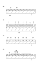
- FIG. 3 is a process diagram showing an example of a method for manufacturing an electronic component device.
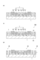
- FIG. 3 is a process diagram showing an example of a method for manufacturing an electronic component device.
- FIG. 3 is a process diagram showing an example of a method for manufacturing an electronic component device.
- FIG. 3 is a process diagram showing an example of a method for manufacturing an electronic component device.
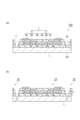
- FIG. 2 is a process diagram showing an example of a method for manufacturing an electronic component device having semiconductor components.
- FIG. 2 is a process diagram showing an example of a method for manufacturing an electronic component device having semiconductor components.
- FIG. 2 is a process diagram showing an example of a method for manufacturing an electronic component device having semiconductor components.
- FIG. 2 is a process diagram showing an example of a method for manufacturing an electronic component device having semiconductor components.
- FIG. 2 is a process diagram showing an example of a method for manufacturing an electronic component device having semiconductor components.
- FIG. 2 is a process diagram showing an example of a method for manufacturing an electronic component device having semiconductor components.
- FIG. 2 is a process diagram showing an example of a method for manufacturing an electronic component device having semiconductor components.
- FIG. 2 is a process diagram showing an example of a method for manufacturing an electronic component device having semiconductor components.
- FIG. 2 is a process diagram showing an example of a method for manufacturing an electronic component device having semiconductor components.
- FIG. 2 is a process diagram showing an example of a method for manufacturing an electronic component device having semiconductor components.
- FIG. 2 is a process diagram showing an example of a method for manufacturing an electronic component device having semiconductor components.
- FIG. 2 is a process diagram showing an example of a method for manufacturing an electronic component device having semiconductor components.
- FIG. 2 is a process diagram showing an example of a method for manufacturing an electronic component device having semiconductor components.
- FIG. 2 is a process diagram showing an example of a method for manufacturing an electronic component device having semiconductor components.
- FIG. 2 is a process diagram showing an example of a method for manufacturing an electronic component device having semiconductor components.
- FIG. 2 is a process diagram showing an example of a method for manufacturing an electronic component device having semiconductor components.
- FIG. 2 is a process diagram showing an example of a method for manufacturing an electronic component device having semiconductor components.
- FIG. 2 is a process diagram showing an example of a method for manufacturing an electronic component device having semiconductor components.
- FIG. 2 is a process diagram showing an example of a method for manufacturing an electronic component device having semiconductor components.
- FIG. 2 is a process diagram showing an example of a method for manufacturing an electronic component device having semiconductor components.
- FIG. 2 is a process diagram showing an example of a method for manufacturing an electronic component device having semiconductor components.
- FIG. 2 is a process diagram showing an example of a method for manufacturing an electronic component device having semiconductor components.
- FIG. 2 is a process diagram showing an example
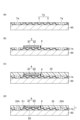
- FIGS. 1 and 2 are process diagrams showing an example of a method for manufacturing an electronic component device.
- the method shown in FIGS. 1 and 2 includes a base material 1 having a first main surface S1 and a second main surface S2 on the back side thereof, an insulating resin layer 3 and a base material 1 provided on the first main surface S1.
- An intermediate structure 10A having a wiring layer 7 having wiring 5 provided in an insulating resin layer 3, and a penetrating portion through which the base material 1 penetrates from the first main surface S1 to the second main surface S2.
- the insulating resin layer 3 forms a trench T having a bottom surface where the penetration part 20A is exposed, and the penetration part is formed along the trench T. 20A, thereby forming a plurality of wiring structures 10 having the divided base material 1 and the wiring layer 7 provided on the base material 1.
- the penetrating portion 20A is a portion of the resin portion 20 that penetrates from the first main surface S1 to the second main surface S2.
- the resin part 20 includes at least the penetrating part 20A, and can be a member integrally formed of a resin material such as a sealing material.
- the entire first principal surface S1 of the base material 1 may be the surface of the resin portion 20.
- a relay wiring portion, a semiconductor component, or both of these, which will be described later, is provided in the base material 1 in addition to the resin portion 20 including the through portion 20A, and the relay wiring portion or the semiconductor component is provided on the first main surface S1. may be exposed to
- the resin part 20 may include resin and inorganic filler.
- the insulating resin layer 3 contains resin and may also contain an inorganic filler.
- the ratio of the volume of the inorganic filler contained in the insulating resin layer 3 to the volume of the insulating resin layer 3 is the ratio of the volume of the inorganic filler contained in the resin part 20 to the volume of the resin part 20. smaller than the percentage. Due to the difference in the proportion of inorganic filler, the resin part 20 is relatively harder.
- Suitable cutting conditions often differ depending on the hardness, but according to the method according to the present disclosure, only the resin part 20 (penetration part 20A) is cut, so the cutting conditions can be cut while avoiding the influence on the insulating resin layer 3. , cutting conditions suitable for cutting the resin portion 20 can be adopted.
- the resin portion 20 (penetrating portion 20A) is cut by, for example, a rotating blade.
- the ratio of the volume of the inorganic filler in the resin part 20 to the volume of the resin part 20 may be, for example, 10 volume % or more and 95 volume % or less.
- the ratio of the volume of the inorganic filler in the insulating resin layer 3 to the volume of the insulating resin layer 3 may be, for example, 0 volume % or more and 50 volume % or less.
- the wiring layer 7 is formed by exposing and developing the photosensitive resin layer 30 formed on the first main surface S1 of the base material 1, so that the wiring opening 35 and the trench forming a pattern layer 3a having a pattern including openings 37, and forming a conductor layer 5a including a via portion 51 filling the opening 35 for wiring, and a wiring pattern portion 52 provided on the pattern layer 3a. It is formed by repeating .
- the insulating resin layer 3 is formed by the first pattern layer 3a, the second pattern layer 3b, and the third pattern layer 3c, which are sequentially formed from the base material 1 side.
- the wiring 5 is formed by the first conductor layer 5a, the second conductor layer 5b, and the third conductor layer 5c, which are sequentially formed from the base material 1 side.
- a trench T penetrating the insulating resin layer 3 is formed by connecting the plurality of trench openings 37 formed by the plurality of pattern layers 3a, 3b, and 3c.
- the photosensitive resin layer 30 and pattern layers 3a, 3b, and 3c can be formed using a normal resist material used for forming an insulating resin layer of a wiring layer.
- actinic light such as ultraviolet rays is irradiated through a mask 9 having openings provided at positions corresponding to the wiring openings 35 and the trench openings 37.
- part of the resin layer 30 is removed by laser irradiation, thereby forming patterned layers 3a, 3b, and 3c having patterns including wiring openings 35 and trench openings 37. It's okay.
- the resin layer 30 may be non-photosensitive.
- the conductor layers 5a, 5b, 5c and the wiring 5 can be formed by a conventional method such as plating, printing of conductor paste, or sputtering.
- the wiring layer 7 is used as a rewiring layer connected to semiconductor components including, for example, IC chips.
- the number of pattern layers and conductor layers constituting the wiring layer 7 is not particularly limited, but may be, for example, 2 or more and 8 or less, respectively.
- the overall thickness of the wiring layer 7 may be, for example, 10 ⁇ m or more and 150 ⁇ m or less.
- the intermediate structure 10A includes forming the wiring layer 7 forming the trench T on a carrier substrate different from the base material 1, and moving the wiring layer 7 from the carrier substrate onto the base material 1. , may be prepared by a method including.
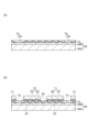
- FIGS. 3 and 4 are process diagrams showing another example of a method for manufacturing an electronic component device.
- the wiring layer 7 forms a pattern layer 3a having a pattern including openings 35 for wiring by exposing and developing the photosensitive resin layer 30, and A conductor layer 5a including a via portion 51 filling the opening 35 of the conductor layer 5a and a wiring pattern portion 52 provided on the pattern layer 3a is repeatedly formed.
- the insulating resin layer 3 is formed by a plurality of pattern layers 3a, 3b, 3c
- the wiring 5 is formed by a plurality of conductor layers 5a, 5b, 5c.
- FIG. 4(f) a portion of the formed insulating resin layer 3 is removed by laser irradiation, thereby forming a trench T.
- a trench T having a width that increases in the direction away from the base material 1 may be formed.
- the width of the trench opening formed by the plurality of pattern layers 3a, 3b, and 3c it is possible to form a trench T having a width that gradually increases.
- the end face of the trench T (insulating resin layer 3) is inclined in this way, the occurrence of cracks or peeling starting from the end of the insulating resin layer 3 can be suppressed.
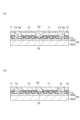
- FIGS. 6 to 9 are process diagrams showing an example of a method for manufacturing an electronic component device having a plurality of semiconductor components.
- the base material 1 forms an internal wiring layer 7A forming an internal trench Ta, and relay wiring on the internal wiring layer 7A. 4 and the copper pillar 8, forming a resin part 20 for sealing the relay wiring part 4, and removing the surface layer part of the resin part 20 on the side opposite to the internal wiring layer 7A, and forming the relay wiring. forming a flat surface from which the portion 4 and the copper pillar 8 are exposed.
- the base material 1 to be formed includes an internal wiring layer 7A, a relay wiring section 4, and a resin section 20.
- the resin portion 20 includes a portion filling the internal trench Ta of the internal wiring layer 7A, and includes a penetrating portion 20A that penetrates from the first main surface S1 to the second main surface S2 on the back side thereof.
- the internal wiring layer 7A is exposed on the second main surface S2 of the base material 1.
- the internal wiring layer 7A can be formed by exposing and developing a photosensitive resin layer, laser irradiation, or a combination thereof, similar to the method shown in FIGS. 1 to 4.
- the relay wiring section 4 includes a main body section 41 including relay wiring electrically connected to a plurality of semiconductor components, and terminals 42 provided on the outer surface of the main body section 41.
- the relay wiring section 4 is arranged on the internal wiring layer 7A in such a direction that the terminals 42 are located on the opposite side of the internal wiring layer 7A.
- the relay wiring section 4 may be a silicon interposer including a silicon substrate.
- the copper pillar 8 can be formed by a conventional method such as plating or printing conductive paste. Copper pillar 8 is electrically connected to wiring 5 in internal wiring layer 7A.
- the resin part 20 can be formed of, for example, a normal sealing material such as a thermosetting resin composition containing an inorganic filler.
- the inorganic filler may include, for example, silica particles.
- a wiring layer 7B is formed on the first main surface S1 of the base material 1 to form a trench Tb having a bottom surface where the through portion 20A is exposed.
- the trench Tb is formed at a position overlapping the internal trench Ta when viewed from the thickness direction of the base material 1.
- the wiring layer 7B can be formed by a method similar to that shown in FIGS. 1 to 4.
- the wiring 5 in the wiring layer 7B is electrically connected to the relay wiring section 4 and the copper pillar 8.
- a plurality of semiconductor components 71 and 72 are mounted on the formed wiring layer 7B (FIG. 7(f)).
- the semiconductor components 71 and 72 each have a bump 55, and the semiconductor components 71 and 72 are electrically connected to the wiring layer 7B by the bump 55.
- the space between semiconductor components 71 and 72 and wiring layer 7B is filled with underfill material 25.
- An intermediate structure 10A having a base material 1, a wiring layer 7B, and semiconductor components 71 and 72 is moved onto a carrier substrate 61 different from the carrier substrate 60 in a direction in which the semiconductor components 71 and 72 are located on the carrier substrate 61 side.
- the bumps 15 are provided on the internal wiring layer 7A (FIG. 7(g)).
- the carrier substrate 62 includes a support substrate 62A and a temporary fixing material layer 62B provided on the support substrate 62A.
- the intermediate structure 10A is temporarily fixed to the carrier substrate 62 with the bumps 15 in contact with the temporary fixing material layer 62B.
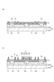
- the penetrating portion 20A of the resin portion 20 is cut from the trench Tb side along the trench Tb and the internal trench Ta, thereby forming a plurality of wiring structures 10 on the carrier substrate 62 (see FIG. 8). i)).
- the wiring structure 10 is peeled off from the carrier substrate 62 ((j) in FIG. 8).
- the wiring structure 10 is an electronic component device, that is, a semiconductor package, including a relay wiring section 4 and a plurality of semiconductor components 71 and 72. A plurality of semiconductor components 71 and 72 are electrically connected via relay wiring section 4 .
- the semiconductor component 71 and the semiconductor component 72 that constitute one wiring structure 10 can be components having different functions.
- the semiconductor component 71 may be a system-on-chip (SoC)
- the semiconductor component 72 may be a memory.
- One wiring structure 10 semiconductor package
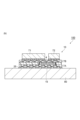
- an electronic component device 100 is obtained by mounting the wiring structure 10 on an organic wiring board 80.
- Wiring structure 10 is electrically connected to organic wiring board 80 via bumps 15 .
- An underfill material 25 may be filled between the wiring structure 10 and the organic wiring substrate 80.
- Various electronic components other than the wiring structure 10 may be further mounted on one organic wiring board 80.
- FIGS. 10 and 11 are process diagrams showing another example of a method for manufacturing an electronic component device having a plurality of semiconductor components.
- the method shown in FIGS. 10 and 11 has the following points: the relay wiring section 4 is arranged on the internal wiring layer 7A with the terminal 42 located on the internal wiring layer 7A side ((b) in FIG. 10), and This method differs from the methods shown in FIGS. 7 to 9 in that a plurality of semiconductor components 71 and 72 are mounted on the internal wiring layer 7A (FIG. 11(f)).
- the bumps 15 are provided on the wiring layer 7B with the intermediate structure 10A temporarily fixed to the carrier substrate 60 ((e) in FIG. 11).
- the penetration portion 20A of the resin portion 20 extends along the trench Tb and the internal trench Ta. are cut from the internal trench Ta side, thereby forming a plurality of wiring structures 10 on the carrier substrate 62.
- the formed wiring structure 10 can be peeled off from the carrier substrate 62 and mounted on an organic wiring board.
- FIGS. 12, 13, 14, 15, 16, 17, and 18 are also process diagrams showing partial cross-sectional views of an example of a method for manufacturing an electronic component device (semiconductor package) having a plurality of semiconductor components.
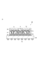
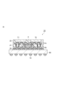
- the base material 1 includes an internal redistribution layer 7A provided inside the first main surface S1 and the second main surface S2, and a plurality of relay wiring sections 4 provided on one main surface S1 side; a first sealing resin layer 21 that seals the relay wiring section 4 between the internal rewiring layer 7A and the rewiring layer 7B; A plurality of semiconductor components 71 and 72 provided on the second main surface S2 side of the internal rewiring layer 7A and a second sealing resin layer 22 that seals the semiconductor components 71 and 72 on the internal rewiring layer 7A. and has.
- the rewiring layer 7B provided on the first main surface S1 of the base material 1 forms a trench Tb having a bottom surface Sb from which the first sealing resin layer 21 is exposed.
- the internal rewiring layer 7A has an internal insulating resin layer and wiring provided within the internal insulating resin layer.
- the internal insulating resin layer and wiring of the internal rewiring layer 7A can have the same configuration as the insulating resin layer and wiring of the above-mentioned wiring layer or internal wiring layer.
- the relay wiring section 4 is connected to the wiring of the internal rewiring layer 7A.
- the semiconductor components 71 and 72 are also connected to the wiring of the internal rewiring layer 7A.
- the relay wiring section 4 may be connected to the wiring of the rewiring layer 7B.
- the internal rewiring layer 7A forms an internal trench Ta having a bottom surface Sa through which the first sealing resin layer 21 is exposed.
- a second sealing resin layer 22 fills the internal trench Ta.
- the second sealing resin layer 22 does not have to completely fill the internal trench Ta.
- the intermediate structure 10A having the base material 1 and the redistribution layer 7B is prepared, and then the penetration portion 20A is cut along the trench Tb and the internal trench Ta. , and a plurality of wiring structures 10 having rewiring layers 7B are formed.
- Each of the plurality of wiring structures 10 to be formed includes a relay wiring section 4 and two or more semiconductor components 71 and 72 electrically connected via the relay wiring section 4.
- the two or more semiconductor components 71 and 72 may be the same or different.
- the semiconductor component 71 may be a system-on-chip (SoC)
- SoC system-on-chip
- the semiconductor component 72 may be a memory.
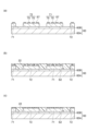
- a carrier substrate 60 having a support substrate 60A and a temporary fixing material layer 60B provided on the support substrate 60A is prepared, On the temporary fixing material layer 60B of 60, an internal rewiring layer 7A is formed which forms an internal trench Ta having a bottom surface Sa through which the carrier substrate 60 (temporary fixing material layer 60B) is exposed.
- the internal rewiring layer 7A can be formed by the same method as the above-mentioned wiring layer.
- the plurality of semiconductor components 71 and 72 are arranged on the opposite side of the internal rewiring layer 7A from the carrier substrate 60.
- the semiconductor components 71 and 72 include a semiconductor chip 70 having a main surface S7 including an integrated circuit, and bumps 55 provided on the main surface S7.
- the semiconductor components 71 and 72 are arranged on the internal rewiring layer 7A in such a direction that the main surface S7 including the integrated circuit is located on the internal rewiring layer 7A side.
- the semiconductor components 71 and 72 may be electrically connected to the wiring of the internal rewiring layer 7A by the bumps 55.
- the space between the semiconductor components 71 and 72 and the internal rewiring layer 7A may be filled with the underfill material 25.
- a second sealing resin layer 22 is formed that seals the semiconductor components 71 and 72 and fills the internal trench Ta.
- the second sealing resin layer 22 is a plate-shaped resin molded body having a second main surface S2.
- the semiconductor components 71 and 72 are sealed inside the second main surface S2.
- a part of the second sealing resin layer 22 may be removed from the second main surface S2 side, thereby forming a surface (second main surface S2) where the semiconductor components 71 and 72 are exposed ( (d) in FIG. 13).
- the second sealing resin layer 22 includes a penetrating portion that penetrates from the second main surface 2 to the bottom surface of the internal trench Ta.
- the second sealing resin layer 22 can be a layer containing a resin and an inorganic filler, which is formed of a resin material such as a normal sealant, as in the example of the resin part 20 described above.
- the second sealing resin layer 22 can be removed by a conventional method such as chemical mechanical polishing.
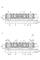
- the carrier substrate 60 is separated from the internal rewiring layer 7A, and the structure including the internal rewiring layer 7A, the semiconductor components 71 and 72, and the second sealing resin layer 22 is placed on another carrier substrate 61.
- the second main surface S2 is temporarily fixed in the direction facing the carrier substrate 61 ((e) in FIG. 14).
- the carrier substrate 61 has a support substrate 61A and a temporary fixing material layer 61B provided on the support substrate 61A.
- the electrode 14 may be provided on the surface of the internal rewiring layer 7A exposed by separation of the carrier substrate 60. Electrode 14 may be formed before carrier substrate 60 is separated, or may be formed after carrier substrate 60 is separated.
- the relay wiring section 4 is an interposer having a semiconductor chip 40 having a main surface S4 including an integrated circuit 43, and terminals 42 provided on the main surface S4.
- Semiconductor chip 40 may have conductive vias 44 connected to terminals 42 .
- the relay wiring section 4 may be arranged on the internal redistribution layer 7A in such a direction that the main surface S4 including the integrated circuit 43 is located on the internal redistribution layer 7A side.
- the copper pillar 8 may be fixed on the electrode 14 arranged around the relay wiring section 4 .
- a first sealing resin layer 21 for sealing the relay wiring section 4 is formed on the internal rewiring layer ((g) in FIG. 15).
- the first sealing resin layer 21 is a plate-shaped resin molded body having a first main surface S1.
- the relay wiring section 4 is sealed inside the first main surface S1.
- a part of the first sealing resin layer 21 is removed from the first main surface S1 side, thereby forming a surface (first main surface S1) where the relay wiring section 4 and the copper pillar 8 are exposed.
- the base material 1 having the first main surface S1 and the second main surface S2 is formed on the carrier substrate 60.
- the resin portion 20 is constituted by the first sealing resin layer 21 and the second sealing resin layer 22.
- the first sealing resin layer 21 includes a penetrating portion that penetrates from the first main surface S1 to the bottom surface of the internal trench Ta.
- the first sealing resin layer 21 can be a layer containing a resin and an inorganic filler, which is formed of a resin material such as a normal sealing material, similarly to the example of the resin part 20 described above.
- the first sealing resin layer 21 can also be removed by a conventional method such as chemical mechanical polishing.
- the first sealing resin layer 21 is formed on the first main surface S1 on the side opposite to the internal rewiring layer 7A of the relay wiring section 4 and the first sealing resin layer 21.
- a rewiring layer 7B forming a trench Tb having an exposed bottom surface Sb is formed.
- the rewiring layer 7B can be formed by the same method as the above-mentioned wiring layer.
- the rewiring layer 7B may have an electrode 14 provided on the surface opposite to the relay wiring section 4.
- the penetrating portion 20A is formed on the carrier substrate 61.
- Bumps 15 may be formed on the electrodes 14 of the rewiring layer 7B before or after the base material 1 is cut.
- the formed wiring structure 10 is separated from the carrier substrate 61 as shown in FIG. 17(l).
- the obtained wiring structure 10 may be used as a semiconductor package.
- the wiring structure 10 is also possible to mount the wiring structure 10 on an organic wiring substrate 80 (semiconductor package substrate) to obtain a semiconductor package having the wiring structure 10 and the semiconductor package substrate (organic wiring substrate 80).
- the space between the wiring structure 10 and the organic wiring board 80 may be filled with an underfill material 25.
- Bumps 15 may be provided on the surface of organic wiring board 80 opposite to wiring structure 10 .
- FIGS. 19, 20, 21, 22, 23, and 24 are also process diagrams showing partial cross-sectional views of an example of a method for manufacturing an electronic component device (semiconductor package) having a plurality of semiconductor components.
- the intermediate structure 10A temporarily fixes the plurality of semiconductor components 71 and 72 on the carrier substrate 60 (FIG. 19(a)), and Forming the second sealing resin layer 22 to be sealed on the carrier substrate 60 (FIG.
- FIG. 21(f) the first sealing resin layer 21 is exposed on the side opposite to the relay wiring section 4 and the internal rewiring layer 7A of the first sealing resin layer 21. 22(j), and providing bumps 15 on the electrodes 14 of the rewiring layer 7B. It is prepared by a method including (k) in FIG. 22. Then, as shown in FIG. By doing so, the wiring structure 10 (semiconductor package) can be obtained.
- the base material 1 includes an internal redistribution layer 7A provided inside the first main surface S1 and the second main surface S2, and a second main surface of the internal redistribution layer 7A.
- a plurality of relay wiring sections 4 provided on one main surface S1 side; a first sealing resin layer 21 that seals the relay wiring section 4 between the internal rewiring layer 7A and the rewiring layer 7B;
- a plurality of semiconductor components 71 and 72 provided on the second main surface S2 side of the internal rewiring layer 7A and a second sealing resin layer 22 that seals the semiconductor components 71 and 72 on the internal rewiring layer 7A. and has.
- the internal rewiring layer 7A forms an internal trench Ta having a bottom surface Sa through which the second sealing resin layer 22 is exposed.
- the first sealing resin layer 21 fills the internal trench Ta.
- the semiconductor components 71 and 72 temporarily fixed on the carrier substrate 60 may include a semiconductor chip 70 having a main surface S7 including an integrated circuit, and terminals 75 provided on the main surface S7.
- the semiconductor components 71 and 72 may be temporarily fixed on the carrier substrate 60 in such a direction that the main surface S7 including the integrated circuit is located on the opposite side of the carrier substrate 60.
- the second sealing resin layer 22 is a plate-shaped resin molded body having a second main surface S2. Before forming the internal rewiring layer 7A, as shown in FIG. 19C, a part of the second sealing resin layer 22 is removed from the side opposite to the carrier substrate 60, and the semiconductor component 71 , 72 may be formed.
- the first sealing resin layer 21 is a plate-shaped resin molded body having a first main surface S1. Before the rewiring layer 7B is formed, as shown in FIG. Also, a surface on which the copper pillar 8 is exposed may be formed.
- the wiring structure 10 is also possible to mount the wiring structure 10 on an organic wiring substrate 80 (semiconductor package substrate) to obtain a semiconductor package having the wiring structure 10 and the semiconductor package substrate (organic wiring substrate 80).
- the space between the wiring structure 10 and the organic wiring board 80 may be filled with an underfill material 25.
- Bumps 15 may be provided on the surface of organic wiring board 80 opposite to wiring structure 10 .
- the resin part 20 may contain a resin and an inorganic filler.
- the insulating resin layer in the rewiring layer 7B may contain an inorganic filler.
- the internal insulating resin layer in the internal rewiring layer 7A may contain an inorganic filler.
- the ratio of the volume of the inorganic filler to the volume of each layer is equal to the resin part of the volume of the inorganic filler contained in the resin part. may be smaller than the proportion of the volume.
- the insulating resin layer of the redistribution layer 7B is smaller than the smallest volume ratio of the inorganic filler in each layer.
- the volume ratio of the inorganic filler in the internal insulating resin layer of the internal redistribution layer 7A may be small.
- the ratio of the volume of the inorganic filler in the first sealing resin layer 21 and the second sealing resin layer 22 to the volume of each layer may be, for example, 10 volume % or more and 95 volume % or less.
- the ratio of the volume of the inorganic filler in the insulating resin layer of the redistribution layer 7B and the internal insulating resin layer of the internal redistribution layer 7A to the volume of the insulating resin layer may be, for example, from 0% by volume to 50% by volume.
- SYMBOLS 1 Base material, 3... Insulating resin layer, 5... Wiring, 3a, 3b, 3c... Pattern layer, 4... Relay wiring part, 5a, 5b, 5c... Conductor layer, 7, 7B... Wiring layer (rewiring layer) , 7A... Internal wiring layer (internal rewiring layer), 10... Wiring structure (semiconductor package), 10A... Intermediate structure, 20... Resin part, 20A... Penetration part, 30... Resin layer, 35... Wiring opening , 37... Opening for trench, 40... Semiconductor chip, 42... Terminal, 43... Integrated circuit, 44... Conductive via, 51... Via portion, 52... Wiring pattern portion, 60, 61, 62...
- Carrier substrate 71, 72... Semiconductor component, 80... Organic wiring board, 100... Electronic component device, S1... First main surface of base material, S2... Second main surface of base material, S7... Main surface including integrated circuit of semiconductor chip , Sa...bottom of internal trench, Sb...bottom of trench, T, Tb...trench, Ta...internal trench.
Landscapes
- Engineering & Computer Science (AREA)
- Microelectronics & Electronic Packaging (AREA)
- Manufacturing & Machinery (AREA)
- Production Of Multi-Layered Print Wiring Board (AREA)
- Physics & Mathematics (AREA)
- Geometry (AREA)
- Internal Circuitry In Semiconductor Integrated Circuit Devices (AREA)
- Printing Elements For Providing Electric Connections Between Printed Circuits (AREA)
Abstract
Description
[1]
第一の主面及びその裏側の第二の主面を有する基材と、前記第一の主面上に設けられ、絶縁樹脂層及び前記絶縁樹脂層内に設けられた配線を有する再配線層とを有する中間構造体であって、前記基材が、前記第一の主面から前記第二の主面まで貫通する貫通部を含む樹脂部を有し、前記再配線層が、前記貫通部が露出する底面を有するトレンチを形成している、中間構造体を準備することと、
前記トレンチに沿って前記貫通部を切断し、それにより分割された前記基材と前記基材上に設けられた前記再配線層とを有する複数の配線構造体を形成することと、
を含み、
前記基材が、
前記第一の主面及び前記第二の主面の内側に設けられ、内部絶縁樹脂層及び前記内部絶縁樹脂層内に設けられた配線を有する内部再配線層と、
前記内部再配線層の前記第一の主面側に設けられ、前記内部再配線層の前記配線と接続された複数の中継配線部と、
前記中継配線部を前記内部再配線層上で封止する第一の封止樹脂層と、
前記内部再配線層の前記第二の主面側に設けられ、前記内部再配線層の前記配線と接続された複数の半導体部品と、
前記半導体部品を前記内部再配線層上で封止する第二の封止樹脂層と、
を有し、
前記内部再配線層が、前記第一の封止樹脂層が露出する底面を有する内部トレンチを形成しており、
前記第二の封止樹脂層が前記内部トレンチを充填し、
前記基材の厚さ方向から見たときに前記トレンチの前記底面と前記内部トレンチの前記底面とが重なっており、
前記樹脂部が、前記第一の封止樹脂層及び前記第二の封止樹脂層を含み、
前記トレンチ及び前記内部トレンチに沿って前記貫通部が切断され、
形成される前記複数の配線構造体が、それぞれ、前記中継配線部と、前記中継配線部を介して電気的に接続された複数の前記半導体部品とを有し、
前記中間構造体が、
キャリア基板上に、前記キャリア基板が露出する底面を有する前記内部トレンチを形成している前記内部再配線層を形成することと、
前記内部再配線層の前記キャリア基板とは反対側に複数の前記半導体部品を配置することと、
前記半導体部品を封止するとともに前記内部トレンチを充填する前記第二の封止樹脂層を前記内部再配線層上に形成することと、
前記内部再配線層から前記キャリア基板を分離することと、
前記内部再配線層の前記半導体部品とは反対側に、複数の前記中継配線部を配置することと、
前記中継配線部を封止する前記第一の封止樹脂層を前記内部再配線層上に形成することと、
前記中継配線部及び前記第一の封止樹脂層の前記内部再配線層とは反対側に、前記第一の封止樹脂層が露出する底面を有する前記トレンチを形成している前記再配線層を形成することと、
を含む方法によって準備される、
半導体パッケージを製造する方法。
[2]
前記半導体部品が、集積回路を含む主面を有する半導体チップを有し、
前記半導体部品が、前記集積回路を含む前記主面が前記内部再配線層側に位置する向きで前記内部再配線層の前記キャリア基板とは反対側に配置される、
[1]に記載の方法。
[3]
前記樹脂部が無機フィラーを含む、[1]又は[2]に記載の方法。
[4]
前記絶縁樹脂層及び前記内部絶縁樹脂層が無機フィラーを含まない、又は、前記絶縁樹脂層及び前記内部絶縁樹脂層が無機フィラーを含み、
前記絶縁樹脂層及び前記内部絶縁樹脂層が無機フィラーを含むとき、前記絶縁樹脂層に含まれる前記無機フィラーの体積の前記絶縁樹脂層の体積に対する割合、及び、前記内部絶縁樹脂層に含まれる前記無機フィラーの体積の前記内部絶縁樹脂層の体積に対する割合が、前記樹脂部に含まれる前記無機フィラーの体積の前記樹脂層の体積に対する割合よりも小さい、
[1]~[3]のいずれかに記載の方法。
[5]
前記再配線層又は前記内部再配線層のうち少なくとも一方が、
感光性の樹脂層の露光及び現像により、前記配線用の開口及び前記トレンチ用の開口を含むパターンを有するパターン層を形成することと、前記配線用の開口を充填するビア部を含む導体層を形成することと、を繰り返すことを含む方法によって形成され、
複数の前記パターン層によって前記絶縁樹脂層が形成され、複数の前記導体層によって前記配線が形成され、複数の前記パターン層によって形成された複数の前記トレンチ用の開口が連結することによって前記トレンチが形成される、
[1]~[4]のいずれかに記載の方法。
[6]
前記再配線層又は前記内部再配線層のうち少なくとも一方が、
樹脂層の一部をレーザー照射によって除去し、それにより前記配線用の開口及び前記トレンチ用の開口を含むパターンを有するパターン層を形成することと、前記配線用の開口を充填するビア部を含む導体層を形成することと、を繰り返すことを含む方法によって形成され、
複数の前記パターン層によって前記絶縁樹脂層が形成され、複数の前記導体層によって前記配線が形成され、複数の前記パターン層によって形成された複数の前記トレンチ用の開口が連結することによって前記トレンチが形成される、
[1]~[4]のいずれかに記載の方法。
[7]
前記再配線層又は前記内部再配線層のうち少なくとも一方が、
感光性の樹脂層の露光及び現像により、前記配線用の開口を含むパターンを有するパターン層を形成することと、前記配線用の開口を充填するビア部を含む導体層を形成することと、を繰り返すことを含む方法によって形成され、
複数の前記パターン層によって前記絶縁樹脂層が形成され、複数の前記導体層によって前記配線が形成され、形成された前記絶縁樹脂層の一部がレーザー照射によって除去され、それにより前記トレンチが形成される、
[1]~[4]のいずれかに記載の方法。
[8]
前記トレンチの幅が、前記基材から離れる方向に向かって拡がっている、[1]~[7]のいずれかに記載の方法。
[9]
前記内部トレンチの幅が、前記第一の封止樹脂層から離れる方向に向かって拡がっている、[1]~[8]のいずれかに記載の方法。
[10]
第一の主面及びその裏側の第二の主面を有する基材と、前記第一の主面上に設けられ、絶縁樹脂層及び前記絶縁樹脂層内に設けられた配線を有する再配線層とを有する中間構造体であって、前記基材が、前記第一の主面から前記第二の主面まで貫通する貫通部を含む樹脂部を有し、前記再配線層が、前記貫通部が露出する底面を有するトレンチを形成している、中間構造体を準備することと、
前記トレンチに沿って前記貫通部を切断し、それにより分割された前記基材と前記基材上に設けられた前記再配線層とを有する複数の配線構造体を形成することと、
を含み、
前記基材が、
前記第一の主面及び前記第二の主面の内側に設けられ、内部絶縁樹脂層及び前記内部絶縁樹脂層内に設けられた配線を有する内部再配線層と、
前記内部再配線層の前記第一の主面側に設けられ、前記内部再配線層の前記配線と接続された複数の中継配線部と、
前記中継配線部を前記内部再配線層上で封止する第一の封止樹脂層と、
前記内部再配線層の前記第二の主面側に設けられ、前記内部再配線層の前記配線と接続された複数の半導体部品と、
前記半導体部品を前記内部再配線上で封止する第二の封止樹脂層と、
を有し、
前記内部再配線層が、前記第二の封止樹脂層が露出する底面を有する内部トレンチを形成しており、
前記第一の封止樹脂層が前記内部トレンチを充填し、
前記基材の厚さ方向から見たときに前記トレンチの前記底面と前記内部トレンチの前記底面とが重なっており、
前記樹脂部が、前記第一の封止樹脂層及び前記第二の封止樹脂層を含み、
前記トレンチ及び前記内部トレンチに沿って前記貫通部が切断され、
形成される前記複数の配線構造体が、それぞれ、前記中継配線部と、前記中継配線部を介して電気的に接続された複数の前記半導体部品とを有し、
前記中間構造体が、
キャリア基板上に複数の前記半導体部品を仮固定することと、
前記半導体部品を封止する前記第二の封止樹脂層を前記キャリア基板上に形成することと、
前記半導体部品及び前記第二の封止樹脂層の前記キャリア基板とは反対側に、前記第二の封止樹脂層が露出する底面を有する前記内部トレンチを形成している前記内部再配線層を形成することと、
前記内部再配線層の前記半導体部品とは反対側に複数の前記中継配線部を配置することと、
前記中継配線部を封止するとともに前記内部トレンチを充填する前記第一の封止樹脂層を前記内部再配線層上に形成することと、
前記中継配線部及び前記第一の封止樹脂層の前記内部再配線層とは反対側に、前記第一の封止樹脂層が露出する底面を有する前記トレンチを形成している前記再配線層を形成することと、
を含む方法によって準備される、
半導体パッケージを製造する方法。
[11]
前記半導体部品が、集積回路を含む主面を有する半導体チップを有し、
前記半導体部品が、前記集積回路を含む前記主面が前記キャリア基板とは反対側に位置する向きで前記キャリア基板上に仮固定される、
[10]に記載の方法。
[12]
前記樹脂部が無機フィラーを含む、[10]又は[11]に記載の方法。
[13]
前記絶縁樹脂層及び前記内部絶縁樹脂層が無機フィラーを含まない、又は、前記絶縁樹脂層及び前記内部絶縁樹脂層が無機フィラーを含み、
前記絶縁樹脂層及び前記内部絶縁樹脂層が無機フィラーを含むとき、前記絶縁樹脂層に含まれる前記無機フィラーの体積の前記絶縁樹脂層の体積に対する割合、及び前記内部絶縁樹脂層に含まれる前記無機フィラーの体積の前記内部絶縁樹脂層の体積に対する割合が、前記樹脂部に含まれる前記無機フィラーの体積の前記樹脂層の体積に対する割合よりも小さい、
[12]に記載の方法。
[14]
前記再配線層又は前記内部再配線層のうち少なくとも一方が、
感光性の樹脂層の露光及び現像により、前記配線用の開口及び前記トレンチ用の開口を含むパターンを有するパターン層を形成することと、前記配線用の開口を充填するビア部を含む導体層を形成することと、を繰り返すことを含む方法によって形成され、
複数の前記パターン層によって前記絶縁樹脂層が形成され、複数の前記導体層によって前記配線が形成され、複数の前記パターン層によって形成された複数の前記トレンチ用の開口が連結することによって前記トレンチが形成される、
[10]~[13]のいずれかに記載の方法。
[15]
前記再配線層又は前記内部再配線層のうち少なくとも一方が、
樹脂層の一部をレーザー照射によって除去し、それにより前記配線用の開口及び前記トレンチ用の開口を含むパターンを有するパターン層を形成することと、前記配線用の開口を充填するビア部を含む導体層を形成することと、を繰り返すことを含む方法によって形成され、
複数の前記パターン層によって前記絶縁樹脂層が形成され、複数の前記導体層によって前記配線が形成され、複数の前記パターン層によって形成された複数の前記トレンチ用の開口が連結することによって前記トレンチが形成される、
[10]~[13]のいずれかに記載の方法。
[16]
前記再配線層又は前記内部再配線層のうち少なくとも一方が、
感光性の樹脂層の露光及び現像により、前記配線用の開口を含むパターンを有するパターン層を形成することと、前記配線用の開口を充填するビア部を含む導体層を形成することと、を繰り返すことを含む方法によって形成され、
複数の前記パターン層によって前記絶縁樹脂層が形成され、複数の前記導体層によって前記配線が形成され、形成された前記絶縁樹脂層の一部がレーザー照射によって除去され、それにより前記トレンチが形成される、
[10]~[13]のいずれかに記載の方法。
[17]
前記トレンチの幅が、前記基材から離れる方向に向かって拡がっている、請求[10]~[16]のいずれかに記載の方法。
[18]
前記内部トレンチの幅が、前記第一の封止樹脂層から離れる方向に向かって拡がっている、[10]~[17]のいずれかに記載の方法。
[19]
前記配線構造体を有機配線基板に搭載することを更に含む、[1]~[18]のいずれかに記載の方法。
第一の主面及びその裏側の第二の主面を有する基材と、前記第一の主面上に設けられ、絶縁樹脂層及び前記絶縁樹脂層内に設けられた配線を有する配線層とを有する中間構造体であって、前記基材が、前記第一の主面から前記第二の主面まで貫通する貫通部を含む樹脂部を有し、前記配線層が、前記貫通部が露出する底面を有するトレンチを形成している、中間構造体を準備することと、
前記トレンチに沿って前記貫通部を切断し、それにより分割された前記基材と前記基材上に設けられた前記配線層とを有する複数の配線構造体を形成することと、を含む、電子部品装置を製造する方法。
[2’]
前記樹脂部が無機フィラーを含み、
前記絶縁樹脂層が無機フィラーを含まない、又は、前記絶縁樹脂層が無機フィラーを含み、
前記絶縁樹脂層が無機フィラーを含むとき、前記絶縁樹脂層に含まれる前記無機フィラーの体積の前記絶縁樹脂層の体積に対する割合が、前記樹脂部に含まれる前記無機フィラーの体積の前記樹脂層の体積に対する割合よりも小さい、
[1’]に記載の方法。
[3’]
前記中間構造体が、前記トレンチを形成している前記配線層を前記基材上に形成することを含む方法によって準備される、[1’]に記載の方法。
[4’]
前記中間構造体が、前記トレンチを形成している前記配線層をキャリア基板上に形成することと、前記配線層を前記キャリア基板上から前記基材上に移動させることと、を含む方法によって準備される、[1’]に記載の方法。
[5’]
前記配線層が、
感光性の樹脂層の露光及び現像により、前記配線用の開口及び前記トレンチ用の開口を含むパターンを有するパターン層を形成することと、前記配線用の開口を充填するビア部を含む導体層を形成することと、を繰り返すことを含む方法によって形成され、
複数の前記パターン層によって前記絶縁樹脂層が形成され、複数の前記導体層によって前記配線が形成され、複数の前記パターン層によって形成された複数の前記トレンチ用の開口が連結することによって前記トレンチが形成される、
[1’]~[4’]のいずれか一項に記載の方法。
[6’]
前記配線層が、
樹脂層の一部をレーザー照射によって除去し、それにより前記配線用の開口及び前記トレンチ用の開口を含むパターンを有するパターン層を形成することと、前記配線用の開口を充填するビア部を含む導体層を形成することと、を繰り返すことを含む方法によって形成され、
複数の前記パターン層によって前記絶縁樹脂層が形成され、複数の前記導体層によって前記配線が形成され、複数の前記パターン層によって形成された複数の前記トレンチ用の開口が連結することによって前記トレンチが形成される、
[1’]~[4’]のいずれか一項に記載の方法。
[7’]
前記配線層が、
感光性の樹脂層の露光及び現像により、前記配線用の開口を含むパターンを有するパターン層を形成することと、前記配線用の開口を充填するビア部を含む導体層を形成することと、を繰り返すことを含む方法によって形成され、
複数の前記パターン層によって前記絶縁樹脂層が形成され、複数の前記導体層によって前記配線が形成され、形成された前記絶縁樹脂層の一部がレーザー照射によって除去され、それにより前記トレンチが形成される、
[1’]~[4’]のいずれか一項に記載の方法。
[8’]
当該方法が、前記配線層上に複数の半導体部品を搭載することを更に含み、
形成される複数の前記配線構造体が、それぞれ1個以上の前記半導体部品を有する、[1’]~[7’]のいずれか一項に記載の方法。
[9’]
前記基材が、前記第二の主面に露出する内部配線層を更に有し、
前記内部配線層が、前記樹脂部の前記貫通部が充填された内部トレンチを形成しており、
当該方法が、前記内部配線層上に複数の半導体部品を搭載することを更に含み、
前記トレンチ及び前記内部トレンチに沿って前記貫通部が切断され、
形成される前記複数の配線構造体が、それぞれ1個以上の前記半導体部品を有する、[1’]~[7’]のいずれか一項に記載の方法。
[10’]
前記基材が、複数の前記半導体部品に電気的に接続される中継配線を有する中継配線部を更に含み、前記中継配線部が前記樹脂部によって封止されており、
形成される前記複数の配線構造体が、それぞれ、前記中継配線部と、前記中継配線部を介して電気的に接続された2個以上の前記半導体部品とを有する、
[8’]又は[9’]に記載の方法。
[11’]
前記トレンチの幅が、前記基材から離れる方向に向かって拡がっている、[1’]~[10’]のいずれか一項に記載の方法。
[12’]
前記配線構造体を有機配線基板に搭載することを更に含む、[1]~[11’]のいずれか一項に記載の方法。
Claims (19)
- 第一の主面及びその裏側の第二の主面を有する基材と、前記第一の主面上に設けられ、絶縁樹脂層及び前記絶縁樹脂層内に設けられた配線を有する再配線層とを有する中間構造体であって、前記基材が、前記第一の主面から前記第二の主面まで貫通する貫通部を含む樹脂部を有し、前記再配線層が、前記貫通部が露出する底面を有するトレンチを形成している、中間構造体を準備することと、
前記トレンチに沿って前記貫通部を切断し、それにより分割された前記基材と前記基材上に設けられた前記再配線層とを有する複数の配線構造体を形成することと、
を含み、
前記基材が、
前記第一の主面及び前記第二の主面の内側に設けられ、内部絶縁樹脂層及び前記内部絶縁樹脂層内に設けられた配線を有する内部再配線層と、
前記内部再配線層の前記第一の主面側に設けられ、前記内部再配線層の前記配線と接続された複数の中継配線部と、
前記中継配線部を前記内部再配線層上で封止する第一の封止樹脂層と、
前記内部再配線層の前記第二の主面側に設けられ、前記内部再配線層の前記配線と接続された複数の半導体部品と、
前記半導体部品を前記内部再配線層上で封止する第二の封止樹脂層と、
を有し、
前記内部再配線層が、前記第一の封止樹脂層が露出する底面を有する内部トレンチを形成しており、
前記第二の封止樹脂層が前記内部トレンチを充填し、
前記基材の厚さ方向から見たときに前記トレンチの前記底面と前記内部トレンチの前記底面とが重なっており、
前記樹脂部が、前記第一の封止樹脂層及び前記第二の封止樹脂層を含み、
前記トレンチ及び前記内部トレンチに沿って前記貫通部が切断され、
形成される前記複数の配線構造体が、それぞれ、前記中継配線部と、前記中継配線部を介して電気的に接続された複数の前記半導体部品とを有し、
前記中間構造体が、
キャリア基板上に、前記キャリア基板が露出する底面を有する前記内部トレンチを形成している前記内部再配線層を形成することと、
前記内部再配線層の前記キャリア基板とは反対側に複数の前記半導体部品を配置することと、
前記半導体部品を封止するとともに前記内部トレンチを充填する前記第二の封止樹脂層を前記内部再配線層上に形成することと、
前記内部再配線層から前記キャリア基板を分離することと、
前記内部再配線層の前記半導体部品とは反対側に、複数の前記中継配線部を配置することと、
前記中継配線部を封止する前記第一の封止樹脂層を前記内部再配線層上に形成することと、
前記中継配線部及び前記第一の封止樹脂層の前記内部再配線層とは反対側に、前記第一の封止樹脂層が露出する底面を有する前記トレンチを形成している前記再配線層を形成することと、
を含む方法によって準備される、
半導体パッケージを製造する方法。 - 前記半導体部品が、集積回路を含む主面を有する半導体チップを有し、
前記半導体部品が、前記集積回路を含む前記主面が前記内部再配線層側に位置する向きで前記内部再配線層の前記キャリア基板とは反対側に配置される、
請求項1に記載の方法。 - 前記樹脂部が無機フィラーを含む、請求項1に記載の方法。
- 前記絶縁樹脂層及び前記内部絶縁樹脂層が無機フィラーを含まない、又は、前記絶縁樹脂層及び前記内部絶縁樹脂層が無機フィラーを含み、
前記絶縁樹脂層及び前記内部絶縁樹脂層が無機フィラーを含むとき、前記絶縁樹脂層に含まれる前記無機フィラーの体積の前記絶縁樹脂層の体積に対する割合、及び、前記内部絶縁樹脂層に含まれる前記無機フィラーの体積の前記内部絶縁樹脂層の体積に対する割合が、前記樹脂部に含まれる前記無機フィラーの体積の前記樹脂層の体積に対する割合よりも小さい、
請求項1に記載の方法。 - 前記再配線層又は前記内部再配線層のうち少なくとも一方が、
感光性の樹脂層の露光及び現像により、前記配線用の開口及び前記トレンチ用の開口を含むパターンを有するパターン層を形成することと、前記配線用の開口を充填するビア部を含む導体層を形成することと、を繰り返すことを含む方法によって形成され、
複数の前記パターン層によって前記絶縁樹脂層が形成され、複数の前記導体層によって前記配線が形成され、複数の前記パターン層によって形成された複数の前記トレンチ用の開口が連結することによって前記トレンチが形成される、
請求項1に記載の方法。 - 前記再配線層又は前記内部再配線層のうち少なくとも一方が、
樹脂層の一部をレーザー照射によって除去し、それにより前記配線用の開口及び前記トレンチ用の開口を含むパターンを有するパターン層を形成することと、前記配線用の開口を充填するビア部を含む導体層を形成することと、を繰り返すことを含む方法によって形成され、
複数の前記パターン層によって前記絶縁樹脂層が形成され、複数の前記導体層によって前記配線が形成され、複数の前記パターン層によって形成された複数の前記トレンチ用の開口が連結することによって前記トレンチが形成される、
請求項1に記載の方法。 - 前記再配線層又は前記内部再配線層のうち少なくとも一方が、
感光性の樹脂層の露光及び現像により、前記配線用の開口を含むパターンを有するパターン層を形成することと、前記配線用の開口を充填するビア部を含む導体層を形成することと、を繰り返すことを含む方法によって形成され、
複数の前記パターン層によって前記絶縁樹脂層が形成され、複数の前記導体層によって前記配線が形成され、形成された前記絶縁樹脂層の一部がレーザー照射によって除去され、それにより前記トレンチが形成される、
請求項1に記載の方法。 - 前記トレンチの幅が、前記基材から離れる方向に向かって拡がっている、請求項1に記載の方法。
- 前記内部トレンチの幅が、前記第一の封止樹脂層から離れる方向に向かって拡がっている、請求項1に記載の方法。
- 第一の主面及びその裏側の第二の主面を有する基材と、前記第一の主面上に設けられ、絶縁樹脂層及び前記絶縁樹脂層内に設けられた配線を有する再配線層とを有する中間構造体であって、前記基材が、前記第一の主面から前記第二の主面まで貫通する貫通部を含む樹脂部を有し、前記再配線層が、前記貫通部が露出する底面を有するトレンチを形成している、中間構造体を準備することと、
前記トレンチに沿って前記貫通部を切断し、それにより分割された前記基材と前記基材上に設けられた前記再配線層とを有する複数の配線構造体を形成することと、
を含み、
前記基材が、
前記第一の主面及び前記第二の主面の内側に設けられ、内部絶縁樹脂層及び前記内部絶縁樹脂層内に設けられた配線を有する内部再配線層と、
前記内部再配線層の前記第一の主面側に設けられ、前記内部再配線層の前記配線と接続された複数の中継配線部と、
前記中継配線部を前記内部再配線層上で封止する第一の封止樹脂層と、
前記内部再配線層の前記第二の主面側に設けられ、前記内部再配線層の前記配線と接続された複数の半導体部品と、
前記半導体部品を前記内部再配線上で封止する第二の封止樹脂層と、
を有し、
前記内部再配線層が、前記第二の封止樹脂層が露出する底面を有する内部トレンチを形成しており、
前記第一の封止樹脂層が前記内部トレンチを充填し、
前記基材の厚さ方向から見たときに前記トレンチの前記底面と前記内部トレンチの前記底面とが重なっており、
前記樹脂部が、前記第一の封止樹脂層及び前記第二の封止樹脂層を含み、
前記トレンチ及び前記内部トレンチに沿って前記貫通部が切断され、
形成される前記複数の配線構造体が、それぞれ、前記中継配線部と、前記中継配線部を介して電気的に接続された複数の前記半導体部品とを有し、
前記中間構造体が、
キャリア基板上に複数の前記半導体部品を仮固定することと、
前記半導体部品を封止する前記第二の封止樹脂層を前記キャリア基板上に形成することと、
前記半導体部品及び前記第二の封止樹脂層の前記キャリア基板とは反対側に、前記第二の封止樹脂層が露出する底面を有する前記内部トレンチを形成している前記内部再配線層を形成することと、
前記内部再配線層の前記半導体部品とは反対側に複数の前記中継配線部を配置することと、
前記中継配線部を封止するとともに前記内部トレンチを充填する前記第一の封止樹脂層を前記内部再配線層上に形成することと、
前記中継配線部及び前記第一の封止樹脂層の前記内部再配線層とは反対側に、前記第一の封止樹脂層が露出する底面を有する前記トレンチを形成している前記再配線層を形成することと、
を含む方法によって準備される、
半導体パッケージを製造する方法。 - 前記半導体部品が、集積回路を含む主面を有する半導体チップを有し、
前記半導体部品が、前記集積回路を含む前記主面が前記キャリア基板とは反対側に位置する向きで前記キャリア基板上に仮固定される、
請求項10に記載の方法。 - 前記樹脂部が無機フィラーを含む、請求項10に記載の方法。
- 前記絶縁樹脂層及び前記内部絶縁樹脂層が無機フィラーを含まない、又は、前記絶縁樹脂層及び前記内部絶縁樹脂層が無機フィラーを含み、
前記絶縁樹脂層及び前記内部絶縁樹脂層が無機フィラーを含むとき、前記絶縁樹脂層に含まれる前記無機フィラーの体積の前記絶縁樹脂層の体積に対する割合、及び前記内部絶縁樹脂層に含まれる前記無機フィラーの体積の前記内部絶縁樹脂層の体積に対する割合が、前記樹脂部に含まれる前記無機フィラーの体積の前記樹脂層の体積に対する割合よりも小さい、
請求項12に記載の方法。 - 前記再配線層又は前記内部再配線層のうち少なくとも一方が、
感光性の樹脂層の露光及び現像により、前記配線用の開口及び前記トレンチ用の開口を含むパターンを有するパターン層を形成することと、前記配線用の開口を充填するビア部を含む導体層を形成することと、を繰り返すことを含む方法によって形成され、
複数の前記パターン層によって前記絶縁樹脂層が形成され、複数の前記導体層によって前記配線が形成され、複数の前記パターン層によって形成された複数の前記トレンチ用の開口が連結することによって前記トレンチが形成される、
請求項10に記載の方法。 - 前記再配線層又は前記内部再配線層のうち少なくとも一方が、
樹脂層の一部をレーザー照射によって除去し、それにより前記配線用の開口及び前記トレンチ用の開口を含むパターンを有するパターン層を形成することと、前記配線用の開口を充填するビア部を含む導体層を形成することと、を繰り返すことを含む方法によって形成され、
複数の前記パターン層によって前記絶縁樹脂層が形成され、複数の前記導体層によって前記配線が形成され、複数の前記パターン層によって形成された複数の前記トレンチ用の開口が連結することによって前記トレンチが形成される、
請求項10に記載の方法。 - 前記再配線層又は前記内部再配線層のうち少なくとも一方が、
感光性の樹脂層の露光及び現像により、前記配線用の開口を含むパターンを有するパターン層を形成することと、前記配線用の開口を充填するビア部を含む導体層を形成することと、を繰り返すことを含む方法によって形成され、
複数の前記パターン層によって前記絶縁樹脂層が形成され、複数の前記導体層によって前記配線が形成され、形成された前記絶縁樹脂層の一部がレーザー照射によって除去され、それにより前記トレンチが形成される、
請求項10に記載の方法。 - 前記トレンチの幅が、前記基材から離れる方向に向かって拡がっている、請求項10に記載の方法。
- 前記内部トレンチの幅が、前記第一の封止樹脂層から離れる方向に向かって拡がっている、請求項10に記載の方法。
- 前記配線構造体を有機配線基板に搭載することを更に含む、請求項1~18のいずれか一項に記載の方法。
Priority Applications (3)
| Application Number | Priority Date | Filing Date | Title |
|---|---|---|---|
| CN202380036147.3A CN119096354A (zh) | 2022-09-02 | 2023-08-31 | 制造半导体封装件的方法 |
| JP2024544590A JPWO2024048762A1 (ja) | 2022-09-02 | 2023-08-31 | |
| KR1020257008917A KR20250061732A (ko) | 2022-09-02 | 2023-08-31 | 반도체 패키지를 제조하는 방법 |
Applications Claiming Priority (2)
| Application Number | Priority Date | Filing Date | Title |
|---|---|---|---|
| PCT/JP2022/033144 WO2024047872A1 (ja) | 2022-09-02 | 2022-09-02 | 電子部品装置を製造する方法 |
| JPPCT/JP2022/033144 | 2022-09-02 |
Publications (1)
| Publication Number | Publication Date |
|---|---|
| WO2024048762A1 true WO2024048762A1 (ja) | 2024-03-07 |
Family
ID=90097951
Family Applications (4)
| Application Number | Title | Priority Date | Filing Date |
|---|---|---|---|
| PCT/JP2022/033144 Ceased WO2024047872A1 (ja) | 2022-09-02 | 2022-09-02 | 電子部品装置を製造する方法 |
| PCT/JP2023/032012 Ceased WO2024048762A1 (ja) | 2022-09-02 | 2023-08-31 | 半導体パッケージを製造する方法 |
| PCT/JP2023/032010 Ceased WO2024048760A1 (ja) | 2022-09-02 | 2023-08-31 | 半導体パッケージを製造する方法 |
| PCT/JP2023/032021 Ceased WO2024048763A1 (ja) | 2022-09-02 | 2023-08-31 | 半導体パッケージを製造する方法 |
Family Applications Before (1)
| Application Number | Title | Priority Date | Filing Date |
|---|---|---|---|
| PCT/JP2022/033144 Ceased WO2024047872A1 (ja) | 2022-09-02 | 2022-09-02 | 電子部品装置を製造する方法 |
Family Applications After (2)
| Application Number | Title | Priority Date | Filing Date |
|---|---|---|---|
| PCT/JP2023/032010 Ceased WO2024048760A1 (ja) | 2022-09-02 | 2023-08-31 | 半導体パッケージを製造する方法 |
| PCT/JP2023/032021 Ceased WO2024048763A1 (ja) | 2022-09-02 | 2023-08-31 | 半導体パッケージを製造する方法 |
Country Status (6)
| Country | Link |
|---|---|
| US (3) | US20250287514A1 (ja) |
| JP (4) | JPWO2024047872A1 (ja) |
| KR (4) | KR20250060885A (ja) |
| CN (4) | CN119073008A (ja) |
| TW (4) | TW202425720A (ja) |
| WO (4) | WO2024047872A1 (ja) |
Families Citing this family (1)
| Publication number | Priority date | Publication date | Assignee | Title |
|---|---|---|---|---|
| CN121241432A (zh) * | 2024-04-30 | 2025-12-30 | 株式会社力森诺科 | 半导体装置的制造方法及配线基板 |
Citations (3)
| Publication number | Priority date | Publication date | Assignee | Title |
|---|---|---|---|---|
| JP2006286967A (ja) * | 2005-03-31 | 2006-10-19 | Fujitsu Ltd | 多層配線基板及びその製造方法 |
| JP2011003758A (ja) * | 2009-06-19 | 2011-01-06 | Shinko Electric Ind Co Ltd | 半導体装置及びその製造方法 |
| WO2012165530A1 (ja) * | 2011-06-03 | 2012-12-06 | 株式会社村田製作所 | 多層基板の製造方法および多層基板 |
Family Cites Families (5)
| Publication number | Priority date | Publication date | Assignee | Title |
|---|---|---|---|---|
| JPH08288647A (ja) * | 1995-04-12 | 1996-11-01 | Fujitsu Ltd | プリント配線板の製造方法及びプリント配線板 |
| WO2014041696A1 (ja) * | 2012-09-14 | 2014-03-20 | 株式会社メイコー | 部品内蔵基板及びその製造方法 |
| JP2018046266A (ja) * | 2016-09-17 | 2018-03-22 | 京セラ株式会社 | 多数個取り配線基板、配線基板および多数個取り配線基板の製造方法 |
| KR20210074645A (ko) | 2019-12-12 | 2021-06-22 | 명전바이오 주식회사 | 수용성 규산염을 포함하는 동물 사료 첨가제 |
| KR20210074646A (ko) | 2019-12-12 | 2021-06-22 | 주식회사 에코리더 | 수상형 태양광모듈 조립체 및 이의 설치방법 |
-
2022
- 2022-09-02 US US18/859,545 patent/US20250287514A1/en active Pending
- 2022-09-02 KR KR1020257009310A patent/KR20250060885A/ko active Pending
- 2022-09-02 JP JP2024543750A patent/JPWO2024047872A1/ja active Pending
- 2022-09-02 CN CN202280095323.6A patent/CN119073008A/zh active Pending
- 2022-09-02 WO PCT/JP2022/033144 patent/WO2024047872A1/ja not_active Ceased
-
2023
- 2023-08-31 CN CN202380036148.8A patent/CN119096355A/zh active Pending
- 2023-08-31 KR KR1020257009088A patent/KR20250061734A/ko active Pending
- 2023-08-31 JP JP2024544591A patent/JPWO2024048763A1/ja active Pending
- 2023-08-31 CN CN202380036147.3A patent/CN119096354A/zh active Pending
- 2023-08-31 KR KR1020257008917A patent/KR20250061732A/ko active Pending
- 2023-08-31 JP JP2024544588A patent/JPWO2024048760A1/ja active Pending
- 2023-08-31 CN CN202380036145.4A patent/CN119096353A/zh active Pending
- 2023-08-31 TW TW112132922A patent/TW202425720A/zh unknown
- 2023-08-31 KR KR1020257008337A patent/KR20250059426A/ko active Pending
- 2023-08-31 US US18/859,166 patent/US20250293105A1/en active Pending
- 2023-08-31 JP JP2024544590A patent/JPWO2024048762A1/ja active Pending
- 2023-08-31 US US18/859,165 patent/US20250259859A1/en active Pending
- 2023-08-31 WO PCT/JP2023/032012 patent/WO2024048762A1/ja not_active Ceased
- 2023-08-31 WO PCT/JP2023/032010 patent/WO2024048760A1/ja not_active Ceased
- 2023-08-31 WO PCT/JP2023/032021 patent/WO2024048763A1/ja not_active Ceased
- 2023-09-01 TW TW112133231A patent/TW202414720A/zh unknown
- 2023-09-01 TW TW112133291A patent/TW202418409A/zh unknown
- 2023-09-01 TW TW112133225A patent/TW202418499A/zh unknown
Patent Citations (3)
| Publication number | Priority date | Publication date | Assignee | Title |
|---|---|---|---|---|
| JP2006286967A (ja) * | 2005-03-31 | 2006-10-19 | Fujitsu Ltd | 多層配線基板及びその製造方法 |
| JP2011003758A (ja) * | 2009-06-19 | 2011-01-06 | Shinko Electric Ind Co Ltd | 半導体装置及びその製造方法 |
| WO2012165530A1 (ja) * | 2011-06-03 | 2012-12-06 | 株式会社村田製作所 | 多層基板の製造方法および多層基板 |
Also Published As
| Publication number | Publication date |
|---|---|
| TW202425720A (zh) | 2024-06-16 |
| WO2024048760A1 (ja) | 2024-03-07 |
| CN119096355A (zh) | 2024-12-06 |
| US20250287514A1 (en) | 2025-09-11 |
| TW202418499A (zh) | 2024-05-01 |
| CN119096353A (zh) | 2024-12-06 |
| KR20250060885A (ko) | 2025-05-07 |
| CN119096354A (zh) | 2024-12-06 |
| KR20250061732A (ko) | 2025-05-08 |
| US20250293105A1 (en) | 2025-09-18 |
| KR20250059426A (ko) | 2025-05-02 |
| JPWO2024047872A1 (ja) | 2024-03-07 |
| CN119073008A (zh) | 2024-12-03 |
| US20250259859A1 (en) | 2025-08-14 |
| KR20250061734A (ko) | 2025-05-08 |
| JPWO2024048763A1 (ja) | 2024-03-07 |
| JPWO2024048760A1 (ja) | 2024-03-07 |
| WO2024048763A1 (ja) | 2024-03-07 |
| TW202418409A (zh) | 2024-05-01 |
| TW202414720A (zh) | 2024-04-01 |
| WO2024047872A1 (ja) | 2024-03-07 |
| JPWO2024048762A1 (ja) | 2024-03-07 |
Similar Documents
| Publication | Publication Date | Title |
|---|---|---|
| CN107393834B (zh) | 内插器、半导体封装和制造内插器的方法 | |
| TWI802210B (zh) | 封裝結構及其製造方法 | |
| JP5102726B2 (ja) | 半導体装置の製造方法 | |
| US11217534B2 (en) | Galvanic corrosion protection for semiconductor packages | |
| TW200905755A (en) | Wafer level package structure and fabrication methods | |
| TW201405735A (zh) | 柵格扇出晶圓級封裝和製造柵格扇出晶圓級封裝的方法 | |
| CN1476631A (zh) | 具有防湿结构的密封管芯封装上的直接组合层 | |
| CN114050132A (zh) | 半导体设备封装及其制造方法 | |
| US12002799B2 (en) | Die stacking structure and method forming same | |
| CN117423680A (zh) | 半导体封装件及其制造方法 | |
| US11521959B2 (en) | Die stacking structure and method forming same | |
| WO2024048760A1 (ja) | 半導体パッケージを製造する方法 | |
| CN104167369B (zh) | 芯片封装结构的制作方法 | |
| CN101207103B (zh) | 半导体封装元件及其制造方法 | |
| TWI309467B (en) | Substrate strip and substrate structure and method for manufacturing the same | |
| US7910478B2 (en) | Method of manufacturing semiconductor devices | |
| TWI849821B (zh) | 電子封裝件及其基板結構 | |
| US20250038043A1 (en) | Dendrite mitigation of passive components | |
| TWI321595B (en) | Circuit substrate and method for fabricating plating through hole | |
| CN104952740A (zh) | 半导体封装及其制造方法 | |
| CN1567584A (zh) | 在芯片上植设导电凸块的半导体封装件及其制法 | |
| CN118943079A (zh) | 玻璃芯基板的制备方法、玻璃芯基板及半导体封装体 | |
| CN121011508A (zh) | 一种芯片封装结构的制作方法及芯片封装结构 | |
| CN108257933B (zh) | 封装结构 |
Legal Events
| Date | Code | Title | Description |
|---|---|---|---|
| 121 | Ep: the epo has been informed by wipo that ep was designated in this application |
Ref document number: 23860524 Country of ref document: EP Kind code of ref document: A1 |
|
| WWE | Wipo information: entry into national phase |
Ref document number: 18859167 Country of ref document: US |
|
| WWE | Wipo information: entry into national phase |
Ref document number: 202380036147.3 Country of ref document: CN |
|
| WWE | Wipo information: entry into national phase |
Ref document number: 2024544590 Country of ref document: JP |
|
| ENP | Entry into the national phase |
Ref document number: 20257008917 Country of ref document: KR Kind code of ref document: A |
|
| NENP | Non-entry into the national phase |
Ref country code: DE |
|
| 122 | Ep: pct application non-entry in european phase |
Ref document number: 23860524 Country of ref document: EP Kind code of ref document: A1 |