WO2024048004A1 - 積層構造体、半導体デバイス及びその製造方法 - Google Patents
積層構造体、半導体デバイス及びその製造方法 Download PDFInfo
- Publication number
- WO2024048004A1 WO2024048004A1 PCT/JP2023/021903 JP2023021903W WO2024048004A1 WO 2024048004 A1 WO2024048004 A1 WO 2024048004A1 JP 2023021903 W JP2023021903 W JP 2023021903W WO 2024048004 A1 WO2024048004 A1 WO 2024048004A1
- Authority
- WO
- WIPO (PCT)
- Prior art keywords
- layer
- semiconductor
- gallium nitride
- alignment layer
- alignment
- Prior art date
- Legal status (The legal status is an assumption and is not a legal conclusion. Google has not performed a legal analysis and makes no representation as to the accuracy of the status listed.)
- Ceased
Links
Images





Classifications
-
- H—ELECTRICITY
- H10—SEMICONDUCTOR DEVICES; ELECTRIC SOLID-STATE DEVICES NOT OTHERWISE PROVIDED FOR
- H10P—GENERIC PROCESSES OR APPARATUS FOR THE MANUFACTURE OR TREATMENT OF DEVICES COVERED BY CLASS H10
- H10P14/00—Formation of materials, e.g. in the shape of layers or pillars
- H10P14/20—Formation of materials, e.g. in the shape of layers or pillars of semiconductor materials
- H10P14/32—Formation of materials, e.g. in the shape of layers or pillars of semiconductor materials characterised by intermediate layers between substrates and deposited layers
- H10P14/3242—Structure
-
- H—ELECTRICITY
- H10—SEMICONDUCTOR DEVICES; ELECTRIC SOLID-STATE DEVICES NOT OTHERWISE PROVIDED FOR
- H10D—INORGANIC ELECTRIC SEMICONDUCTOR DEVICES
- H10D30/00—Field-effect transistors [FET]
- H10D30/01—Manufacture or treatment
- H10D30/015—Manufacture or treatment of FETs having heterojunction interface channels or heterojunction gate electrodes, e.g. HEMT
-
- H—ELECTRICITY
- H10—SEMICONDUCTOR DEVICES; ELECTRIC SOLID-STATE DEVICES NOT OTHERWISE PROVIDED FOR
- H10D—INORGANIC ELECTRIC SEMICONDUCTOR DEVICES
- H10D30/00—Field-effect transistors [FET]
- H10D30/40—FETs having zero-dimensional [0D], one-dimensional [1D] or two-dimensional [2D] charge carrier gas channels
- H10D30/47—FETs having zero-dimensional [0D], one-dimensional [1D] or two-dimensional [2D] charge carrier gas channels having two-dimensional [2D] charge carrier gas channels, e.g. nanoribbon FETs or high electron mobility transistors [HEMT]
- H10D30/471—High electron mobility transistors [HEMT] or high hole mobility transistors [HHMT]
- H10D30/475—High electron mobility transistors [HEMT] or high hole mobility transistors [HHMT] having wider bandgap layer formed on top of lower bandgap active layer, e.g. undoped barrier HEMTs such as i-AlGaN/GaN HEMTs
- H10D30/4755—High electron mobility transistors [HEMT] or high hole mobility transistors [HHMT] having wider bandgap layer formed on top of lower bandgap active layer, e.g. undoped barrier HEMTs such as i-AlGaN/GaN HEMTs having wide bandgap charge-carrier supplying layers, e.g. modulation doped HEMTs such as n-AlGaAs/GaAs HEMTs
-
- H—ELECTRICITY
- H10—SEMICONDUCTOR DEVICES; ELECTRIC SOLID-STATE DEVICES NOT OTHERWISE PROVIDED FOR
- H10D—INORGANIC ELECTRIC SEMICONDUCTOR DEVICES
- H10D62/00—Semiconductor bodies, or regions thereof, of devices having potential barriers
- H10D62/10—Shapes, relative sizes or dispositions of the regions of the semiconductor bodies; Shapes of the semiconductor bodies
- H10D62/17—Semiconductor regions connected to electrodes not carrying current to be rectified, amplified or switched, e.g. channel regions
- H10D62/351—Substrate regions of field-effect devices
- H10D62/357—Substrate regions of field-effect devices of FETs
-
- H—ELECTRICITY
- H10—SEMICONDUCTOR DEVICES; ELECTRIC SOLID-STATE DEVICES NOT OTHERWISE PROVIDED FOR
- H10D—INORGANIC ELECTRIC SEMICONDUCTOR DEVICES
- H10D62/00—Semiconductor bodies, or regions thereof, of devices having potential barriers
- H10D62/40—Crystalline structures
-
- H—ELECTRICITY
- H10—SEMICONDUCTOR DEVICES; ELECTRIC SOLID-STATE DEVICES NOT OTHERWISE PROVIDED FOR
- H10D—INORGANIC ELECTRIC SEMICONDUCTOR DEVICES
- H10D62/00—Semiconductor bodies, or regions thereof, of devices having potential barriers
- H10D62/40—Crystalline structures
- H10D62/405—Orientations of crystalline planes
-
- H—ELECTRICITY
- H10—SEMICONDUCTOR DEVICES; ELECTRIC SOLID-STATE DEVICES NOT OTHERWISE PROVIDED FOR
- H10P—GENERIC PROCESSES OR APPARATUS FOR THE MANUFACTURE OR TREATMENT OF DEVICES COVERED BY CLASS H10
- H10P14/00—Formation of materials, e.g. in the shape of layers or pillars
- H10P14/20—Formation of materials, e.g. in the shape of layers or pillars of semiconductor materials
-
- H—ELECTRICITY
- H10—SEMICONDUCTOR DEVICES; ELECTRIC SOLID-STATE DEVICES NOT OTHERWISE PROVIDED FOR
- H10P—GENERIC PROCESSES OR APPARATUS FOR THE MANUFACTURE OR TREATMENT OF DEVICES COVERED BY CLASS H10
- H10P14/00—Formation of materials, e.g. in the shape of layers or pillars
- H10P14/20—Formation of materials, e.g. in the shape of layers or pillars of semiconductor materials
- H10P14/29—Formation of materials, e.g. in the shape of layers or pillars of semiconductor materials characterised by the substrates
- H10P14/2924—Structures
-
- H—ELECTRICITY
- H10—SEMICONDUCTOR DEVICES; ELECTRIC SOLID-STATE DEVICES NOT OTHERWISE PROVIDED FOR
- H10P—GENERIC PROCESSES OR APPARATUS FOR THE MANUFACTURE OR TREATMENT OF DEVICES COVERED BY CLASS H10
- H10P14/00—Formation of materials, e.g. in the shape of layers or pillars
- H10P14/20—Formation of materials, e.g. in the shape of layers or pillars of semiconductor materials
- H10P14/34—Deposited materials, e.g. layers
- H10P14/3402—Deposited materials, e.g. layers characterised by the chemical composition
- H10P14/3414—Deposited materials, e.g. layers characterised by the chemical composition being group IIIA-VIA materials
- H10P14/3416—Nitrides
-
- H—ELECTRICITY
- H10—SEMICONDUCTOR DEVICES; ELECTRIC SOLID-STATE DEVICES NOT OTHERWISE PROVIDED FOR
- H10D—INORGANIC ELECTRIC SEMICONDUCTOR DEVICES
- H10D30/00—Field-effect transistors [FET]
- H10D30/40—FETs having zero-dimensional [0D], one-dimensional [1D] or two-dimensional [2D] charge carrier gas channels
- H10D30/47—FETs having zero-dimensional [0D], one-dimensional [1D] or two-dimensional [2D] charge carrier gas channels having two-dimensional [2D] charge carrier gas channels, e.g. nanoribbon FETs or high electron mobility transistors [HEMT]
- H10D30/471—High electron mobility transistors [HEMT] or high hole mobility transistors [HHMT]
- H10D30/475—High electron mobility transistors [HEMT] or high hole mobility transistors [HHMT] having wider bandgap layer formed on top of lower bandgap active layer, e.g. undoped barrier HEMTs such as i-AlGaN/GaN HEMTs
-
- H—ELECTRICITY
- H10—SEMICONDUCTOR DEVICES; ELECTRIC SOLID-STATE DEVICES NOT OTHERWISE PROVIDED FOR
- H10D—INORGANIC ELECTRIC SEMICONDUCTOR DEVICES
- H10D62/00—Semiconductor bodies, or regions thereof, of devices having potential barriers
- H10D62/80—Semiconductor bodies, or regions thereof, of devices having potential barriers characterised by the materials
- H10D62/85—Semiconductor bodies, or regions thereof, of devices having potential barriers characterised by the materials being Group III-V materials, e.g. GaAs
- H10D62/8503—Nitride Group III-V materials, e.g. AlN or GaN
-
- H—ELECTRICITY
- H10—SEMICONDUCTOR DEVICES; ELECTRIC SOLID-STATE DEVICES NOT OTHERWISE PROVIDED FOR
- H10D—INORGANIC ELECTRIC SEMICONDUCTOR DEVICES
- H10D64/00—Electrodes of devices having potential barriers
- H10D64/20—Electrodes characterised by their shapes, relative sizes or dispositions
- H10D64/23—Electrodes carrying the current to be rectified, amplified, oscillated or switched, e.g. sources, drains, anodes or cathodes
- H10D64/251—Source or drain electrodes for field-effect devices
- H10D64/256—Source or drain electrodes for field-effect devices for lateral devices wherein the source or drain electrodes are recessed in semiconductor bodies
Definitions
- One embodiment of the present invention relates to a stacked structure, a semiconductor device, and a manufacturing method thereof using a semiconductor layer containing gallium nitride.
- gallium nitride-based semiconductor layers As semiconductor devices using gallium nitride-based semiconductor layers, for example, transistor elements such as HEMT (High Electron Mobility Transistor) and light emitting elements such as LED (Light Emitting Diode) are known. In particular, there is a high demand for light emitting devices using light emitting diodes (LEDs) in each pixel, and there is an urgent need to develop a technology for forming a highly crystalline gallium nitride semiconductor layer on a substrate other than a silicon substrate.
- HEMT High Electron Mobility Transistor
- LED Light Emitting Diode
- Patent Document 1 discloses that a buffer layer is formed on an insulating substrate such as a sapphire substrate or a quartz glass substrate, an insulating pattern is formed on the buffer layer, and a gallium nitride-based semiconductor is formed on the buffer layer and the insulating pattern. Techniques for forming layers are disclosed.
- a gallium nitride-based semiconductor layer is generally formed by epitaxial growth at a temperature exceeding 1000°C using a sapphire substrate, a quartz glass substrate, or the like having heat resistance of 1000°C or higher.
- a temperature exceeding 1000°C using a sapphire substrate, a quartz glass substrate, or the like having heat resistance of 1000°C or higher.
- the use of expensive sapphire substrates or quartz glass substrates hinders the increase in the area of the display screen.
- An object of an embodiment of the present invention is to form a stacked structure using a highly crystalline gallium nitride semiconductor layer on an inexpensive amorphous substrate.
- Another object of an embodiment of the present invention is to form a stacked structure using a highly crystalline gallium nitride semiconductor layer with high throughput.
- a laminated structure in an embodiment of the present invention includes an amorphous substrate having an insulating surface, an alignment layer having a pattern on the amorphous substrate, and a semiconductor layer containing gallium nitride having a pattern on the upper surface of the alignment layer.
- the first angle between the bottom surface and the side surface of the alignment layer is 60° or more and 90° or less.
- a method for manufacturing a laminated structure includes forming an alignment film on an amorphous substrate having an insulating surface, forming an alignment layer having a pattern by etching the alignment film, and forming an alignment layer with a pattern.
- a first semiconductor film containing gallium nitride is formed on the top surface and the side surface of the alignment layer, and the first semiconductor film formed on the side surface of the alignment layer is etched to form a first semiconductor film having a pattern on the top surface of the alignment layer.
- the angle between the bottom surface and the side surface of the alignment layer is 60° or more and 90° or less.
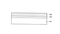
- FIG. 3 is an end view showing a method for manufacturing a laminated structure using a semiconductor layer containing gallium nitride in the first embodiment.
- FIG. 3 is an end view showing a method for manufacturing a laminated structure using a semiconductor layer containing gallium nitride in the first embodiment.
- FIG. 3 is an end view showing a method for manufacturing a laminated structure using a semiconductor layer containing gallium nitride in the first embodiment.
- FIG. 3 is an end view showing a method for manufacturing a laminated structure using a semiconductor layer containing gallium nitride in the first embodiment.
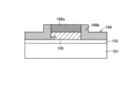
- FIG. 3 is an end view showing a method for manufacturing a laminated structure using a semiconductor layer containing gallium nitride in the first embodiment.
- FIG. 3 is an end view showing a method for manufacturing a laminated structure using a semiconductor layer containing gallium nitride in the first embodiment.
- FIG. 3 is an end view showing a method for manufacturing a laminated structure using a semiconductor layer containing gallium nitride in the first embodiment.
- FIG. 1 is an end view showing a semiconductor device including a stacked structure according to a first embodiment.
- FIG. 1 is a plan view showing a light emitting device using a semiconductor device including a stacked structure according to a first embodiment.
- FIG. 3 is an end view showing a method for manufacturing a laminated structure using a semiconductor layer containing gallium nitride in the first embodiment.
- FIG. 3 is an end view showing a method for manufacturing a laminated structure using a semiconductor layer containing gallium nitride in the first embodiment.
- FIG. 1 is an end view showing a semiconductor device including a stacked structure according to a first embodiment.
- FIG. 1 is a plan view showing a light emitting device using a semiconductor device including a stacked structure according to a first embodiment.
- FIG. 3 is an end view showing a method for manufacturing
- FIG. 3 is an end view showing a method for manufacturing a laminated structure using a semiconductor layer containing gallium nitride in the first embodiment.
- FIG. 3 is an end view showing a method for manufacturing a laminated structure using a semiconductor layer containing gallium nitride in the first embodiment.
- FIG. 2 is an end view showing a method for manufacturing a laminated structure using a semiconductor layer containing gallium nitride in the first embodiment.
- FIG. 3 is an end view showing a method for manufacturing a laminated structure using a semiconductor layer containing gallium nitride in the first embodiment.
- FIG. 7 is an end view showing a semiconductor device including a stacked structure according to a second embodiment.
- the direction from the substrate toward the semiconductor layer will be referred to as "up”, and the opposite direction will be referred to as “down”.
- the expressions “above” and “below” merely explain the vertical relationship of each element.
- the expressions “above” or “below” include not only the case where the third element is interposed between the first element and the second element, but also the case where the third element is not interposed.
- the expressions “above” or “below” include not only cases in which each element overlaps in plan view, but also cases in which they do not overlap.
- elements having the same functions as the elements already described may be denoted by the same reference numerals or the same reference numerals and symbols such as alphabets, and the explanation thereof may be omitted.
- a symbol such as an alphabet may be added to the code indicating the element to distinguish the parts.
- the reference numeral indicating the element will be used in the description.
- ⁇ includes A, B, or C
- ⁇ includes any of A, B, and C
- ⁇ is selected from the group consisting of A, B, and C
- expressions such as “including one of the combinations A to C” do not exclude the case where ⁇ includes multiple combinations of A to C. Furthermore, these expressions do not exclude cases where ⁇ includes other elements.
- FIGS. 1 to 6 are end views showing a method for manufacturing a laminated structure having a patterned semiconductor layer containing gallium nitride according to the first embodiment.
- FIGS. 1 to 6 show an example in which a semiconductor layer including a patterned gallium nitride layer is formed on an amorphous substrate. Note that although FIGS. 1 to 6 show an example in which a single semiconductor layer is formed, in reality, a plurality of semiconductor layers are formed on a substrate.
- a base film 102 is formed on an amorphous substrate 101.
- a glass substrate can be used as the amorphous substrate 101. It is preferable that the glass substrate has a low content of alkali components, a low coefficient of thermal expansion, a high strain point, and a high surface flatness. For example, it is preferable that the content of alkali metals (such as sodium) is 0.1% or less, the thermal expansion coefficient is lower than 50 ⁇ 10 ⁇ 7 /°C, and the strain point is 600°C or higher.
- a gallium nitride-based semiconductor film is formed by a sputtering method, so a glass substrate having lower heat resistance than a sapphire substrate or a quartz substrate can be used.
- a glass substrate is cheaper than a sapphire substrate or a quartz substrate, and is suitable for increasing the area of mother glass.
- the amorphous substrate 101 of this embodiment is not limited to a glass substrate, and may be a resin substrate such as a polyimide substrate, an acrylic substrate, a siloxane substrate, or a fluororesin substrate.
- the base film 102 has a role as a protective film that prevents impurities from being mixed in from the amorphous substrate 101.
- the base film 102 is composed of one or more films selected from, for example, a silicon nitride film, a silicon oxide film, an aluminum nitride film, and an aluminum oxide film.
- the alignment film 103 is formed on the base film 102.
- the alignment film 103 has a function of improving the crystal orientation of the semiconductor film 106 containing gallium nitride when forming the semiconductor film 106 containing gallium nitride (see FIG. 3), which will be described later.
- the alignment film 103 may be conductive or insulative, but preferably has crystallinity oriented along a specific axis (for example, the c-axis).
- the alignment film 103 is preferably a crystal with rotational symmetry, for example, it is preferable that the crystal surface has six-fold rotational symmetry.
- the alignment film 103 preferably has a hexagonal close-packed structure, a face-centered cubic structure, or a structure similar thereto.
- a structure similar to a hexagonal close-packed structure or a face-centered cubic structure includes a crystal structure in which the c-axis does not form 90 degrees with respect to the a-axis and the b-axis.
- the alignment film 103 having a hexagonal close-packed structure or a structure similar thereto is preferably aligned in the [001] direction with respect to the amorphous substrate 101, that is, in the c-axis direction.
- the alignment film 103 having a face-centered cubic structure or a similar structure is preferably oriented in the [111] direction with respect to the amorphous substrate 101.
- the surface condition of the alignment film 103 affects the crystallinity of the semiconductor film 106 containing gallium nitride, which will be described later, it is desirable that the surface of the alignment film 103 be flat.
- the arithmetic mean roughness (Ra) of the surface of the alignment film 103 is smaller than 2.3 nm.
- the above-mentioned alignment film 103 is, for example, a conductive alignment film made of titanium (Ti), titanium nitride (TiNx), titanium oxide (TiOx), graphene, zinc oxide (ZnO), magnesium diboride (MgB2), Aluminum (Al), silver (Ag), calcium (Ca), nickel (Ni), copper (Cu), strontium (Sr), rhodium (Rh), palladium (Pd), cerium (Ce), ytterbium (Yb), Iridium (Ir), platinum (Pt), gold (Au), lead (Pb), actinium (Ac), thorium (Th), BiLaTiO, BiFeO, BaFeO, ZnFeO, PMnN-PZT, or the like can be used.
- a titanium layer is used as the alignment film 103.
- the above-mentioned alignment film 103 is, for example, an insulating alignment film, such as aluminum nitride (AlN), aluminum oxide (Al 2 O 3 ), lithium niobate (LiNbO), BiLaTiO, SrFeO, BiFeO, BaFeO, ZnFeO. , PMnN-PZT, biological apatite (BAp), or the like can be used.
- AlN aluminum nitride
- Al 2 O 3 aluminum oxide
- LiNbO lithium niobate
- BiLaTiO LiNbO
- SrFeO BiFeO
- BaFeO BaFeO
- ZnFeO. boronO
- PMnN-PZT biological apatite
- BAp biological apatite
- the alignment film 103 may be a conductive alignment film or an insulating alignment film. When there is no need to distinguish between the conductive alignment film and the insulating alignment film, they are expressed as an alignment film 103.
- the thickness of the alignment film 103 is, for example, 50 nm or more (preferably 50 nm or more and 100 nm or less).
- the alignment film 103 can be formed by any method.
- the alignment film 103 can be formed by a sputtering method, a CVD method, a vacuum evaporation method, an electron beam evaporation method, or the like.
- the alignment layer 105 having a pattern is formed by etching the alignment film 103 using the resist mask 104.
- the alignment layer 105 has a slope (hereinafter referred to as "taper") in which the angle between the bottom surface and the side surface is ⁇ 1 .
- the taper angle ⁇ 1 of the alignment layer 105 can be set to 60° or more and 90° or less.
- the taper angle ⁇ 1 tends to become small, and depending on the conditions, the taper angle ⁇ 1 becomes less than 60°.
- the taper angle ⁇ 1 of the alignment layer 105 is less than 60°, the area of the taper of the alignment layer 105 becomes larger than when the angle ⁇ 1 is 60° or more and 90° or less.
- the semiconductor film 106 containing gallium nitride formed on the taper of the alignment layer 105 tends to have lower crystallinity than the semiconductor film 106 containing gallium nitride formed on the upper surface of the alignment layer 105. Therefore, as this area increases, the semiconductor film 106 containing gallium nitride with low crystallinity occupies a wider area in the semiconductor film 106 containing gallium nitride.
- the semiconductor film 106 containing gallium nitride with low crystallinity is formed on the taper of the alignment layer 105
- the semiconductor film 106 containing gallium nitride with low crystallinity is formed on the tapered alignment layer 105.
- Crystal growth of the semiconductor film 106 containing gallium may be inhibited. Therefore, in this embodiment, in order to prevent such inhibition of crystal growth, the area of the taper of the alignment layer 105 is suppressed, and in order to suppress the area, the taper angle ⁇ 1 of the alignment layer 105 is A dry etching method is used so that the angle is 60° or more and 90° or less.
- a semiconductor film 106 containing gallium nitride is formed to cover the alignment layer 105.
- a semiconductor film 106 containing gallium nitride is formed as a semiconductor film by a sputtering method.
- the semiconductor film 106 containing gallium nitride is formed by heating an amorphous substrate 101 having an insulating surface (here, an amorphous substrate 101 provided with a base film 102) at 25 to 600°C, preferably 25 to 400°C. It is formed by a sputtering method in a heated state. That is, the semiconductor film 106 containing gallium nitride is formed at a temperature below the strain point of the amorphous substrate 101.
- Gallium nitride is usually formed by MOCVD (metal organic chemical vapor deposition).
- MOCVD metal organic chemical vapor deposition
- the MOCVD method requires a high process temperature, it is not suitable as a method for forming a gallium nitride film in consideration of the heat resistance of the amorphous substrate 101.
- the semiconductor film 106 containing gallium nitride can be formed on the inexpensive amorphous substrate 101 by using a sputtering method.
- the semiconductor film 106 containing gallium nitride can be formed, for example, by sputtering using a sintered body of gallium nitride as a sputtering target and using argon (Ar) or a mixed gas of argon (Ar) and nitrogen (N2) as the sputtering gas. It is formed.
- argon Ar
- Ar argon
- N2 nitrogen
- the sputtering method for example, a bipolar sputtering method, a magnetron sputtering method, a dual magnetron sputtering method, a facing target sputtering method, an ion beam sputtering method, and an inductively coupled plasma (ICP) sputtering method can be applied.
- ICP inductively coupled plasma
- the conductivity type of the semiconductor film 106 containing gallium nitride may be substantially intrinsic, or may have n-type conductivity or p-type conductivity.
- the gallium nitride layer having n-type conductivity may not contain a dopant for controlling valence electrons, or may be doped with silicon (Si) or germanium (Ge) as an n-type dopant. good.
- the gallium nitride layer having p-type conductivity may be doped with an element selected from magnesium (Mg), zinc (Zn), cadmium (Cd), and beryllium (Be) as a p-type dopant. .
- the carrier concentration is preferably 1 ⁇ 10 18 /cm 3 or more.
- the carrier concentration is preferably 5 ⁇ 10 16 /cm 3 or more.
- zinc (Zn) may be included as a dopant.
- the semiconductor film 106 containing gallium nitride may contain one or more elements selected from indium (In), aluminum (Al), and arsenic (As). These elements can adjust the band gap of the semiconductor film 106 containing gallium nitride.
- the semiconductor film 106 containing gallium nitride is formed on the amorphous substrate 101 on which the alignment layer 105 is formed.
- the semiconductor film 106 containing gallium nitride formed on the alignment layer 105 is influenced by the alignment axis of the alignment layer 105.
- the alignment layer 105 has rotational symmetry or c-axis orientation crystallinity
- the semiconductor film 106 containing gallium nitride also has c-axis orientation or (111) orientation crystallinity.
- the crystallinity of the semiconductor film 106 containing gallium nitride is preferably single crystal, but may be polycrystalline, microcrystalline, or nanocrystalline.
- the crystal structure of the semiconductor film 106 containing gallium nitride may have a wurtzite structure.
- the orientation of the semiconductor film 106 containing gallium nitride is preferably c-axis orientation or (111) orientation.
- the semiconductor film 106 containing gallium nitride may have an amorphous structure near the interface where it contacts the alignment layer 105, but preferably has crystallinity in bulk.
- the thickness of the semiconductor film 106 containing gallium nitride is not limited and can be set as appropriate depending on the structure of the device.
- the semiconductor film 106 containing gallium nitride may have a single layer structure, or may have a laminated structure including a plurality of layers having different conductivity types and/or compositions.
- the semiconductor film 106 containing gallium nitride formed on the alignment layer 105 has a first portion 106a that reflects the crystallinity of the alignment layer 105, and a first portion 106a that is more crystalline than the first portion 106a. and a lower second portion 106b.
- the first portion 106a is a portion located above the alignment layer 105.
- the second portion 106b includes a portion located above the base film 102.
- FIG. 3 shows an example in which the taper angle ⁇ 1 is 90°, if ⁇ 1 is smaller than 90°, such as 80°, as described above, the second portion 106b It also includes a portion located above the side surface (tapered portion). Note that in the alignment layer 105, a case where the angle between the bottom surface and the side surface is 90 degrees is also included in the taper angle ⁇ 1 for convenience.
- the taper angle ⁇ 1 of the alignment layer 105 is 60° or more and 90° or less, and the area of the taper of the alignment layer 105 is suppressed. There is little inhibition of growth.
- the first portion 106a reflecting the crystallinity of the alignment layer 105 and the second portion 106b having lower crystallinity than the first portion 106a can be observed with a transmission electron microscope (TEM) to determine the crystallinity. You can check the difference.
- TEM transmission electron microscope
- a resist mask 107 is formed so as to overlap the first portion 106a of the semiconductor film 106 containing gallium nitride. That is, the resist mask 107 is arranged so as to pattern the first portion 106a of the semiconductor film 106 containing gallium nitride located on the upper surface of the alignment layer 105.
- the side surface of the first portion 106a and the side surface of the resist mask 107 are shown to coincide with each other, but the width of the resist mask 107 is narrower than the width of the first portion 106a. It can also be wide.
- the semiconductor film 106 containing gallium nitride is etched using a resist mask 107 to form a patterned semiconductor layer 108 containing gallium nitride.
- a dry etching method using a halogenated gas is used to etch the semiconductor film 106 containing gallium nitride.
- the etching conditions are changed to the second because the etching resistance of the highly crystalline first portion 106a located on the upper surface of the alignment layer 105 is higher than that of the second portion 106b.
- the width of the semiconductor layer 108 located on the upper surface of the alignment layer 105 can be formed without reducing the width to a greater extent than the width of the resist mask 107.
- the resist mask 107 is removed.
- dry type resist peeling or wet type resist peeling can be used.
- the semiconductor layer 108 of the laminated structure 10 of this embodiment is formed by patterning the first portion 106a of the semiconductor film 106 containing gallium nitride, so that it has a specific orientation axis reflecting the orientation of the orientation layer 105. It has uniform crystallinity.
- the first portion 106a formed on the upper surface of the alignment layer 105 is less susceptible to inhibition of crystal growth by the second portion 106b of the semiconductor film containing gallium nitride with low crystallinity.
- the semiconductor layer 108 containing gallium nitride that matches the design of the resist mask 107 can be formed. Therefore, by processing the stacked structure 10 having the semiconductor layer 108 of this embodiment and using it in a semiconductor device, a semiconductor device with excellent characteristics can be realized.
- FIG. 7 is an end view showing a semiconductor device 500 having the stacked structure 10 in the first embodiment.
- a semiconductor device 500 shown in FIG. 7 is an example of an LED element manufactured using the stacked structure 10 shown in FIG. 6. 6 and 7, the thickness relationship between the alignment layer 105 and the semiconductor layer 108 is different, but for convenience of explanation, the thickness of the alignment layer 105 is only exaggerated in FIG. 6. .
- an n-type gallium nitride layer 501, a light-emitting layer 502, and a p-type gallium nitride layer 503 are sequentially grown on the semiconductor layer 108. Thereafter, parts of the n-type gallium nitride layer 501, the light emitting layer 502, and the p-type gallium nitride layer 503 are removed so that the n-type gallium nitride layer 501 is exposed. Finally, an n-type electrode 504 and a p-type electrode 505 are formed in contact with the n-type gallium nitride layer 501 and the p-type gallium nitride layer 503, respectively.
- the semiconductor device 500 shown in FIG. 7 is completed.
- the semiconductor device 500 of this embodiment is formed using a semiconductor layer 108 using only a highly crystalline first portion 106a of a semiconductor film 106 containing gallium nitride formed on an amorphous substrate 101. Therefore, according to this embodiment, the semiconductor device 500 can be manufactured on the inexpensive amorphous substrate 101. Furthermore, according to this embodiment, the semiconductor film 106 containing highly crystalline gallium nitride can be formed by sputtering, so the semiconductor device 500 can be manufactured with high throughput without being exposed to high temperatures throughout the process. be able to.
- the semiconductor device 500 shown in FIG. 7 is merely an example of an LED element, and may be an LED element with another structure.
- the light emitting layer 502 may have a quantum well structure in which gallium nitride layers and indium gallium nitride layers are alternately stacked.
- FIG. 8 is a plan view showing a light emitting device 600 using the semiconductor device 500 having the stacked structure 10 in the first embodiment.
- a display section 601 and a peripheral circuit section 602 are provided on the amorphous substrate 101.
- a terminal section 603 for inputting various signals (video signals and control signals) to the light emitting device 600 is provided in a part of the peripheral circuit section 602.
- a plurality of pixels 604 are arranged in a matrix.
- the semiconductor device 500 shown in FIG. 7 is arranged in each pixel 604.
- each pixel 604 may be provided with a semiconductor chip for controlling light emission and non-light emission of the semiconductor device 500.
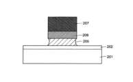
- FIG. 9 is an end view showing the configuration of a laminated structure 20 according to an embodiment of the present invention. First, the state shown in FIG. 4 is obtained according to the process described using FIGS. 1 to 4 of the first embodiment.
- the semiconductor film containing gallium nitride (semiconductor film 106 containing gallium nitride shown in FIG. 4) is etched using a resist mask 207 to form a patterned semiconductor layer 208.
- the amorphous substrate 201, base film 202, resist mask 207, and alignment layer 205 shown in FIG. 9 correspond to the amorphous substrate 101, base film 102, resist mask 107, and alignment layer 105 in FIG. 4, respectively.
- the resist mask 207 is removed to obtain the laminated structure 20.
- the alignment layer 205 has a width between the top surface and the bottom surface that is smaller than the width of the top surface and the width of the bottom surface.
- the width W1 of a cross section taken along a plane parallel to the bottom surface is smaller than the width W2 of the bottom surface of the semiconductor layer 208; It is smaller than the width W3 of the bottom surface of the alignment layer 205.
- the width W2 of the bottom surface of the semiconductor layer 208 is smaller than the width W3 of the bottom surface of the alignment layer 205
- the width W1 of the cross section taken along a plane parallel to the bottom surface of the alignment layer 205 is It is sufficient that the width W2 of the bottom surface of the semiconductor layer 208 is smaller than the width W2 of the bottom surface and the width W3 of the bottom surface of the alignment layer 205, and the width W2 of the bottom surface of the semiconductor layer 208 may be larger than or equal to the width W3 of the bottom surface of the alignment layer 205.
- FIG. 11 is an end view showing the configuration of a laminated structure 30 according to an embodiment of the present invention. first. The state shown in FIG. 3 is obtained according to the process described using FIGS. 1 to 3 of the first embodiment.
- a first semiconductor film 306-1 containing gallium nitride is formed on the first semiconductor film 306-1 containing gallium nitride (semiconductor film 106 containing gallium nitride shown in FIG. 3).
- a second semiconductor film 306-2 containing gallium nitride having the same composition ratio is formed.
- the second semiconductor film 306-2 containing gallium nitride formed on the first semiconductor film 306-1 has a first portion 306-2a and a second portion 306-2b.
- the first portion 306-2a is located on the first portion 306-1a of the first semiconductor film 306-1
- the second portion 306-2b is located on the second portion 306-1b of the first semiconductor film 306-1. located above. Therefore, the crystallinity of the first portion 306-2a is higher than that of the second portion 306-2b.
- the crystallinity of the first portion 306-1a of the first semiconductor film 306-1 and the crystallinity of the first portion 306-2a of the second semiconductor film 306-2 are different from each other in the first semiconductor film 306-1a on the alignment layer 305.
- the crystallinity of the first portion 306-1a of No. 1 is higher.
- a resist mask 307 is formed on the first portion 306-2a of the second semiconductor film 306-2.
- the resist mask 307 is formed to have the same width as the first portion 306-2a of the second semiconductor film 306-2, but the resist mask 307 has a width wider than the first portion 306-2a. It may also be narrow.
- the first semiconductor film 306-1 is etched onto the alignment layer 305.
- a first semiconductor layer 308-1 corresponding to the portion 306-1a and a second semiconductor layer 308-2 corresponding to the first portion 306-2a of the second semiconductor film can be formed.
- the second portion 306-1b of the first semiconductor film 306-1 and the second portion 306-2b of the second semiconductor film 306-2 are selectively etched, so as described above.
- the first portion 306-1a and the first portion 306-2a having high crystallinity become the semiconductor layer 308.
- the etching resistance of the first portion 306-1a tends to be higher. Therefore, due to the etching performed when forming the semiconductor layer 308, the width of the first semiconductor layer 308-1 corresponding to the first portion 306-1a having higher etching resistance is reduced to the width of the first portion 306-1a of the second semiconductor film.
- the width may be larger than the width of the second semiconductor layer 308-2 corresponding to 2a.
- the width of the bottom surface of the first semiconductor layer 308-1 may be larger than the width of the bottom surface of the second semiconductor layer 308-2.
- the resist mask 307 is removed to obtain the laminated structure 30.
- the second semiconductor layer 308-2 laminated thereon also has high crystallinity, and therefore has high crystallinity.
- the semiconductor layer 308 can be obtained with a large thickness. Therefore, by processing the stacked structure 30 having the semiconductor layer 308 of this embodiment and using it in a semiconductor device, a semiconductor device with excellent characteristics can be realized.
- ⁇ Second embodiment> an example will be described in which a semiconductor device having a structure different from that in the first embodiment is formed. Specifically, in this embodiment, an example will be described in which a HEMT (High Electron Mobility Transistor) is formed as a semiconductor device.
- HEMT High Electron Mobility Transistor
- FIG. 15 is an end view showing a semiconductor device 700 including a gallium nitride-based semiconductor layer in the fourth embodiment.
- a semiconductor device 700 shown in FIG. 15 is an example of a HEMT manufactured using the stacked structure 10 shown in FIG. 6 in the first embodiment. Note that in FIGS. 6 and 15, the relationship in thickness between the alignment layer 105 and the semiconductor layer 108 is different, but for convenience of explanation, the thickness of the alignment layer 105 is only exaggerated in FIG. 6. .
- an n-type aluminum gallium nitride layer 701 and an n-type aluminum gallium nitride layer 702 are sequentially formed.
- a sputtering method can be used to form these gallium nitride-based semiconductor layers.
- a trench reaching the n-type aluminum gallium nitride layer 701 is provided in the n-type aluminum gallium nitride layer 701 and the n-type aluminum gallium nitride layer 702, and a source electrode 703 and a drain electrode 704 are arranged inside the trench.
- a gate electrode 705 in contact with the n-type aluminum gallium nitride layer 702 is arranged between the source electrode 703 and the drain electrode 704 .
- a silicon nitride layer 706 is formed as a protective layer, and the HEMT shown in FIG. 15 is completed.
- the semiconductor device 700 of this embodiment is formed using a highly crystalline gallium nitride layer (semiconductor layer 108) formed on the amorphous substrate 101. Therefore, according to this embodiment, the semiconductor device 700 can be manufactured on the inexpensive amorphous substrate 101. Further, according to this embodiment, since the plurality of gallium nitride semiconductor layers are formed by sputtering, the semiconductor device 700 can be manufactured with high throughput without being exposed to high temperatures throughout the process. Note that the semiconductor device 700 shown in FIG. 15 is only an example of a HEMT, and a HEMT of another structure may be used.
Abstract
積層構造体は、絶縁表面を有するアモルファス基板と、アモルファス基板の上のパターンを有する配向層と、配向層の上面にパターンを有する窒化ガリウムを含む半導体層と、を有し、配向層の底面と側面とがなす角の角度は、60°以上90°以下である。また、配向層の底面と上面との間において、底面と平行な面で切った配向層の切断面の幅は、配向層の底面の幅より小さくともよい。さらに、配向層の底面と上面との間において、底面と平行な面で切った配向層の切断面の幅は、半導体層の底面の幅より小さくともよい。
Description
本発明の一実施形態は、窒化ガリウムを含む半導体層を用いた積層構造体、半導体デバイス及びその製造方法に関する。
近年、窒化ガリウム(GaN)を含む半導体層(以下、「窒化ガリウム系半導体層」という)を用いた半導体デバイスの開発が進んでいる。窒化ガリウム系半導体層を用いた半導体デバイスとしては、例えば、HEMT(High Electron Mobility Transistor)などのトランジスタ素子、LED(Light Emitting Diode)などの発光素子が知られている。特に、発光ダイオード(LED)を各画素に用いた発光装置の需要は高く、シリコン基板以外の基板上に、結晶性の高い窒化ガリウム系半導体層を形成する技術の開発が急がれている。例えば、特許文献1には、サファイア基板、石英ガラス基板等の絶縁基板上にバッファ層を形成し、そのバッファ層の上に絶縁パターンを形成し、バッファ層及び絶縁パターンの上に窒化ガリウム系半導体層を形成する技術が開示されている。
上記従来技術のように、一般的には、1000℃以上の耐熱性を有するサファイア基板や石英ガラス基板等を用い、1000℃を超える温度下で窒化ガリウム系半導体層をエピタキシャル成長により形成する。しかしながら、発光表示装置への応用を考慮すると、高価なサファイア基板や石英ガラス基板の使用は、表示画面の大面積化への妨げになるという問題がある。また、1000℃を超える温度下での処理は、処理開始時の昇温及び処理終了時の降温に時間がかかり、スループットが低下するという問題もある。
本発明の一実施形態の課題は、安価なアモルファス基板上に結晶性の高い窒化ガリウム系半導体層を用いて積層構造体を形成することにある。
また、本発明の一実施形態の課題は、結晶性の高い窒化ガリウム系半導体層を用いた積層構造体を高いスループットで形成することにある。
本発明の一実施形態における積層構造体は、絶縁表面を有するアモルファス基板と、アモルファス基板の上のパターンを有する配向層と、配向層の上面にパターンを有する窒化ガリウムを含む半導体層と、を有し、配向層の底面と側面とがなす第1角の角度は、60°以上90°以下である。
本発明の一実施形態における積層構造体の製造方法は、絶縁表面を有するアモルファス基板の上に配向膜を成膜し、配向膜をエッチングすることによりパターンを有する配向層を形成し、配向層の上面と配向層の側面とに窒化ガリウムを含む第1半導体膜を成膜し、配向層の側面に成膜された第1半導体膜をエッチングすることにより、配向層の上面にパターンを有する第1半導体層を形成することを含み、配向層の底面と側面とがなす角は、60°以上90°以下である。
以下、本発明の実施形態について、図面等を参照しつつ説明する。但し、本発明は、その要旨を逸脱しない範囲において様々な態様で実施することができる。本発明は、以下に例示する実施形態の記載内容に限定して解釈されるものではない。図面は、説明をより明確にするため、実際の態様に比べ、各部の幅、厚さ、形状等について模式的に表される場合がある。しかしながら、図面は、あくまで一例であって、本発明の解釈を限定するものではない。
本発明の実施形態を説明する際、基板から半導体層に向かう方向を「上」とし、その逆の方向を「下」とする。ただし、「上に」又は「下に」という表現は、単に、各要素の上下関係を説明しているにすぎない。また、「上に」又は「下に」という表現は、第1要素と第2要素との間に第3要素が介在する場合だけでなく、介在しない場合をも含む。さらに、「上に」又は「下に」という表現は、平面視において各要素が重畳する場合だけでなく、重畳しない場合をも含む。
本発明の実施形態を説明する際、既に説明した要素と同様の機能を備えた要素については、同一の符号又は同一の符号にアルファベット等の記号を付して、説明を省略すること
がある。また、ある要素の部分について区別して説明する必要がある場合は、その要素を示す符号にアルファベット等の記号を付して区別する場合がある。ただし、その要素の各部分について、特に区別する必要がない場合は、その要素を示す符号のみを用いて説明する。
がある。また、ある要素の部分について区別して説明する必要がある場合は、その要素を示す符号にアルファベット等の記号を付して区別する場合がある。ただし、その要素の各部分について、特に区別する必要がない場合は、その要素を示す符号のみを用いて説明する。
本発明の実施形態を説明する際、「αはA、BまたはCを含む」、「αはA、BおよびCのいずれかを含む」、「αはA、BおよびCからなる群から選択される一つを含む」、といった表現は、特に明示が無い限り、αがA~Cの複数の組み合わせを含む場合を排除しない。さらに、これらの表現は、αが他の要素を含む場合も排除しない。
<第1実施形態>
図1~図6は、第1実施形態におけるパターンを有する窒化ガリウムを含む半導体層を有する積層構造体の製造方法を示す端面図である。特に、図1~図6では、アモルファス基板上にパターンを有する窒化ガリウム層を含む半導体層を形成する例を示す。なお、図1~図6では、単一の半導体層を形成する例を示しているが、実際には、基板上に複数の半導体層が形成される。
図1~図6は、第1実施形態におけるパターンを有する窒化ガリウムを含む半導体層を有する積層構造体の製造方法を示す端面図である。特に、図1~図6では、アモルファス基板上にパターンを有する窒化ガリウム層を含む半導体層を形成する例を示す。なお、図1~図6では、単一の半導体層を形成する例を示しているが、実際には、基板上に複数の半導体層が形成される。
まず、図1に示すように、アモルファス基板101上に下地膜102を形成する。アモルファス基板101としては、例えば、ガラス基板を用いることができる。ガラス基板は、アルカリ成分の含有率が低く、熱膨張係数が低く、歪み点が高く、表面の平坦性が高いことが好ましい。例えば、アルカリ金属(ナトリウム等)の含有率が0.1%以下であり、熱膨張係数が50×10-7/℃より低く、歪み点が600℃以上であることが好ましい。後述するように、本実施形態では、スパッタリング法により窒化ガリウム系半導体膜を形成するため、サファイア基板や石英基板に比べて耐熱性の低いガラス基板を用いることができる。このようなガラス基板は、サファイア基板や石英基板に比べて安価であり、マザーガラスの大面積化にも適している。ただし、本実施形態のアモルファス基板101は、ガラス基板に限らず、ポリイミド基板、アクリル基板、シロキサン基板、フッ素樹脂基板などの樹脂基板であってもよい。
下地膜102は、アモルファス基板101からの不純物の混入を防ぐ保護膜としての役割を有する。下地膜102としては、例えば、窒化シリコン膜、酸化シリコン膜、窒化アルミニウム及び酸化アルミニウム膜から選ばれた1又は複数の膜で構成される。
下地膜102の上には、配向膜103が形成される。配向膜103は、後述する窒化ガリウムを含む半導体膜106(図3参照)を形成する際に、窒化ガリウムを含む半導体膜106の結晶の配向性を向上させる機能を有する。
配向膜103は、導電性であっても絶縁性であってもよいが、特定の軸(例えば、c軸)に配向した結晶性を有することが好ましい。配向膜103は、回転対称性を有する結晶であることが好ましく、例えば、その結晶表面が6回回転対称を有することが好ましい。また、配向膜103は、六方最密構造、面心立方構造、又はこれらに準ずる構造を有することが好ましい。ここで、六方最密構造又は面心立方構造に準ずる構造とは、a軸およびb軸に対してc軸が90度にならない結晶構造を含む。六方最密構造又はこれに準ずる構造を有する配向膜103は、アモルファス基板101に対して[001]方向、すなわち、c軸方向に配向していることが好ましい。面心立方構造又はこれに準ずる構造を有する配向膜103は、アモルファス基板101に対して[111]方向に配向していることが好ましい。
配向膜103の表面状態は、後述する窒化ガリウムを含む半導体膜106の結晶性に影響を与えるため、配向膜103の表面は、平坦であることが望ましい。例えば、配向膜103は、表面の算術平均粗さ(Ra)が2.3nmより小さいことが好ましい。
上述の配向膜103としては、例えば、導電性配向膜であり、チタン(Ti)、窒化チタン(TiNx)、酸化チタン(TiOx)、グラフェン、酸化亜鉛(ZnO)、二ホウ化マグネシウム(MgB2)、アルミニウム(Al)、銀(Ag)、カルシウム(Ca)、ニッケル(Ni)、銅(Cu)、ストロンチウム(Sr)、ロジウム(Rh)、パラジウム(Pd)、セリウム(Ce)、イッテルビウム(Yb)、イリジウム(Ir)、白金(Pt)、金(Au)、鉛(Pb)、アクチニウム(Ac)、トリウム(Th)、BiLaTiO、BiFeO、BaFeO、ZnFeO、またはPMnN-PZTなどを用いることができる。特に、導電性配向膜として、チタン、グラフェン、酸化亜鉛、を用いることが好ましい。本実施形態では、配向膜103としてチタン層を用いる。
また、上述の配向膜103としては、例えば、絶縁性配向膜であり、窒化アルミニウム(AlN)、酸化アルミニウム(Al2O3)、ニオブ酸リチウム(LiNbO)、BiLaTiO、SrFeO、BiFeO、BaFeO、ZnFeO、PMnN-PZT、または生体アパタイト(BAp)などを用いることができる。特に絶縁性配向膜として窒化アルミニウム、または酸化アルミニウムを用いることが好ましい。本実施形態では、絶縁性配向膜として、窒化アルミニウム層を用いることが好ましい。
本明細書等において、配向膜103は導電性配向膜であっても良く、絶縁性配向膜であっても良い。導電性配向膜及び絶縁性配向膜を区別する必要が無い場合は配向膜103と表現する。
配向膜103の膜厚は、例えば、50nm以上(好ましくは、50nm以上100nm以下)である。配向膜103は、任意の方法で形成することができる。例えば、配向膜103は、スパッタリング法、CVD法、真空蒸着法、電子ビーム蒸着法等により形成することができる。
次に、図2に示すように、レジストマスク104を用いて配向膜103をエッチングすることにより、パターンを有する配向層105を形成する。配向層105は、底面と側面とがなす角の角度がθ1である勾配(以下、「テーパー」という)を有する。このとき、本実施形態では、配向膜103のエッチングにドライエッチング法を用いるため、配向層105のテーパーの角度θ1を、60°以上90°以下とすることができる。
配向膜103のエッチングにウェットエッチング法を用いた場合、テーパーの角度θ1が小さくなりやすく、条件によってはテーパーの角度θ1が60°未満になる。例えば、配向層105のテーパーの角度θ1が60°未満であった場合、角度θ1が60°以上90°以下のときに比べ、配向層105のテーパーの面積は大きくなる。配向層105のテーパー上に形成される窒化ガリウムを含む半導体膜106は、配向層105の上面に形成される窒化ガリウムを含む半導体膜106に比べ、結晶性が低くなる傾向にある。したがって、この面積が大きくなることにより、結晶性の低い窒化ガリウムを含む半導体膜106が窒化ガリウムを含む半導体膜106中により広く占有することとなる。
さらに、配向層105のテーパーの上に結晶性の低い窒化ガリウムを含む半導体膜106が形成される場合、結晶性の低い窒化ガリウムを含む半導体膜106は、配向層105上に成膜される窒化ガリウムを含む半導体膜106の結晶成長を阻害する場合がある。したがって、本実施形態では、そのような結晶成長の阻害を防止するため、配向層105のテーパーの面積の抑制をし、また、その面積の抑制のために、配向層105のテーパー角のθ1が60°以上90°以下となるように、ドライエッチング法を採用している。
次に、図3に示すように、配向層105を覆うように窒化ガリウムを含む半導体膜106を形成する。本実施形態では、半導体膜として、窒化ガリウムを含む半導体膜106をスパッタリング法により形成する。具体的には、窒化ガリウムを含む半導体膜106は、例えば、絶縁表面を有するアモルファス基板101(ここでは、下地膜102が設けられたアモルファス基板101)を25~600℃、好ましくは25~400℃に加熱した状態でスパッタリング法により形成される。つまり、窒化ガリウムを含む半導体膜106は、アモルファス基板101の歪み点以下の温度で形成される。窒化ガリウムは、通常、MOCVD法(有機金属化学気相成長法)で形成される。しかしながら、MOCVD法はプロセス温度が高いため、アモルファス基板101の耐熱性を考慮すると、窒化ガリウムの成膜方法としては適切ではない。しかしながら、本実施形態では、スパッタリング法を用いることにより、安価なアモルファス基板101上に窒化ガリウムを含む半導体膜106を形成することができる。
窒化ガリウムを含む半導体膜106は、例えば、窒化ガリウムの焼結体をスパッタリングターゲットとし、スパッタガスとしてアルゴン(Ar)又はアルゴン(Ar)及び窒素(N2)の混合ガスを用いてスパッタリングを行うことにより形成される。スパッタリング法としては、例えば、2極スパッタリング法、マグネトロンスパッタリング法、デュアルマグネトロンスパッタリング法、対向ターゲットスパッタリング法、イオンビームスパッタリング法、誘導結合プラズマ(ICP)スパッタリング法を適用することができる。
窒化ガリウムを含む半導体膜106の導電型は、実質的に真性であってもよいし、n型の導電性又はp型の導電性を有していてもよい。n型の導電性を有する窒化ガリウム層は、価電子制御を行うためのドーパントが含まれていなくてもよいし、n型ドーパントとして、シリコン(Si)又はゲルマニウム(Ge)が添加されていてもよい。p型の導電性を有する窒化ガリウム層は、p型ドーパントとして、マグネシウム(Mg)、亜鉛(Zn)、カドミウム(Cd)、ベリリウム(Be)から選ばれた一種の元素が添加されていてもよい。窒化ガリウムを含む半導体膜106にn型ドーパントを添加する場合は、キャリア濃度を1×10¹⁸/cm3以上とすることが好ましい。窒化ガリウムを含む半導体膜106にp型ドーパントを添加する場合は、キャリア濃度を5×1016/cm3以上とすることが好ましい。また、窒化ガリウムを含む半導体膜106を実質的に真性にする場合、ドーパントとして亜鉛(Zn)が含まれていてもよい。
また、窒化ガリウムを含む半導体膜106には、インジウム(In)、アルミニウム(Al)、ヒ素(As)から選ばれた一種又は複数種の元素が含まれていてもよい。これらの元素によって、窒化ガリウムを含む半導体膜106のバンドギャップを調整することができる。
以上のように、本実施形態では、配向層105が形成されたアモルファス基板101上に窒化ガリウムを含む半導体膜106が形成される。このとき、配向層105の上に形成された窒化ガリウムを含む半導体膜106は、配向層105の配向軸の影響を受ける。例えば、配向層105が回転対称性又はc軸配向の結晶性を有する場合、窒化ガリウムを含む半導体膜106もc軸配向又は(111)配向の結晶性を有する。窒化ガリウムを含む半導体膜106の結晶性は、単結晶であることが好ましいが、多結晶、微結晶、又はナノ結晶であってもよい。窒化ガリウムを含む半導体膜106の結晶構造は、ウルツ鉱構造を有していてもよい。窒化ガリウムを含む半導体膜106の配向は、c軸配向又は(111)配向であることが望ましい。窒化ガリウムを含む半導体膜106は、配向層105と接する界面近傍にアモルファス構造が含まれてもよいが、バルクでは結晶性を有していることが好ましい。
窒化ガリウムを含む半導体膜106の膜厚に限定はなく、デバイスの構造に応じて適宜設定することができる。窒化ガリウムを含む半導体膜106は単層構造であってもよいし、導電型及び/又は組成が異なる複数の層を含む積層構造であってもよい。
図3に示すように、配向層105の上に形成された窒化ガリウムを含む半導体膜106は、配向層105の結晶性が反映された第1部分106aと、第1部分106aよりも結晶性が低い第2部分106bとを含む。第1部分106aは、配向層105の上に位置する部分である。第2部分106bは、下地膜102の上に位置する部分を含む。また、図3では、テーパーの角度θ1が90°の例を示したが、例えばθ1が80°等の90°より小さい場合、上述したように、第2部分106bは、配向層105の側面(テーパー部分)の上に位置する部分も含む。なお、配向層105において、底面と側面とがなす角が90°である場合も、便宜上テーパーの角度θ1に含む。
第1部分106aは、上述したように、配向層105のテーパーの角度θ1が60°以上90°以下であり、配向層105のテーパーの面積が抑制されているため、第2部分106bによる結晶成長の阻害は少ない。
配向層105の結晶性が反映された第1部分106aと第1部分106aよりも結晶性の低い第2部分106bは、透過電子顕微鏡(TEM:Transmission Electron Microscope)などで観察することで、結晶性の違いを確認することができる。
次に、図4に示すように、窒化ガリウムを含む半導体膜106の第1部分106aに重畳するように、レジストマスク107を形成する。すなわち、レジストマスク107は、窒化ガリウムを含む半導体膜106のうち、配向層105の上面の上に位置する第1部分106aをパターン化するように配置される。本実施形態では、第1部分106aの側面とレジストマスク107の側面とが一致するように図示しているが、この例に限らず、レジストマスク107の幅は、第1部分106aの幅より狭くてもよく、また、広くてもよい。
次に、図5に示すように、レジストマスク107を用いて窒化ガリウムを含む半導体膜106に対してエッチングを行い、パターンを有する窒化ガリウムを含む半導体層108を形成する。本実施形態では、窒化ガリウムを含む半導体膜106のエッチングに、ハロゲン化ガスを用いたドライエッチング法を用いる。
上述した窒化ガリウムを含む半導体膜106に対して行うエッチングにおいて、配向層105の上面に位置する結晶性の高い第1部分106aのエッチング耐性が第2部分106bに比べ高いため、エッチング条件を第2部分106bに合わせることで、配向層105の上面に位置する半導体層108の幅をレジストマスク107の幅より大きく減らすことなく形成することができる。
次に、レジストマスク107の除去を行う。レジストマスク107の除去には、ドライタイプのレジスト剥離またはウェットタイプのレジスト剥離を用いることができる。
以上の工程を経て、図6に示す積層構造体10が得られる。本実施形態の積層構造体10の半導体層108は、窒化ガリウムを含む半導体膜106の第1部分106aをパターン化したものであるため、配向層105の配向性を反映して特定の配向軸に揃った結晶性を有している。また、配向層105のテーパーの角度が大きいため、結晶性の低い窒化ガリウムを含む半導体膜の第2部分106bによる結晶成長の阻害を配向層105の上面に形成される第1部分106aがあまり受けず、よって、エッチング耐性が高いため、レジストマスク107の設計に合った窒化ガリウムを含む半導体層108を形成することができる。したがって、本実施形態の半導体層108を有する積層構造体10を加工して半導体デバイスに用いることにより、優れた特性の半導体デバイスを実現することができる。
図7は、第1実施形態における積層構造体10を有する半導体デバイス500を示す端面図である。具体的には、図7に示す半導体デバイス500は、図6に示した積層構造体10を用いて製造したLED素子の一例である。なお、図6及び図7において、配向層105と半導体層108との間の膜厚の大小関係が異なるが、説明の便宜上、図6では配向層105の膜厚を誇張しているにすぎない。
図6に示したように、半導体層108を形成したら、半導体層108の上に、n型窒化ガリウム層501、発光層502及びp型窒化ガリウム層503を順次成長させる。その後、n型窒化ガリウム層501、発光層502及びp型窒化ガリウム層503の一部を、n型窒化ガリウム層501が露出するように除去する。最後に、n型窒化ガリウム層501及びp型窒化ガリウム層503にそれぞれ接するn型電極504及びp型電極505を形成する。
以上のプロセスを経て、図7に示した半導体デバイス500が完成する。本実施形態の半導体デバイス500は、アモルファス基板101上に形成された窒化ガリウムを含む半導体膜106のうち、結晶性の高い第1部分106aのみを用いた半導体層108を用いて形成される。したがって、本実施形態によれば、安価なアモルファス基板101上に半導体デバイス500を製造することができる。さらに、本実施形態によれば、結晶性の高い窒化ガリウムを含む半導体膜106をスパッタリング法により形成できるため、プロセス全体を通じて高い温度に曝されることがなく、高いスループットで半導体デバイス500を製造することができる。
図7に示した半導体デバイス500は、LED素子としての一例を示すにすぎず、他の構造のLED素子であってもよい。例えば、発光層502は、窒化ガリウム層と窒化インジウムガリウム層とを交互に積層した量子井戸構造であってもよい。
図8は、第1実施形態に積層構造体10を有する半導体デバイス500を用いた発光装置600を示す平面図である。図8に示すように、アモルファス基板101上には、表示部601及び周辺回路部602が設けられる。周辺回路部602の一部には、発光装置600へ各種信号(映像信号及び制御信号)を入力するための端子部603が設けられる。表示部601の内側には、複数の画素604がマトリクス状に配置される。図7に示した半導体デバイス500は、各画素604に配置されている。図示は省略するが、各画素604には、半導体デバイス500の発光及び非発光を制御するための半導体チップが設けられていてもよい。
以下では、本実施形態に係る積層構造体10のいくつかの変形例について説明する。なお、図面において、第1実施形態と同じ要素については、同じ符号を付して重複する説明を省略する。
<変形例1>
図9は、本発明の一実施形態に係る積層構造体20の構成を示す端面図である。まず、第1実施形態の図1乃至図4を用いて説明したプロセスにしたがって、図4に示す状態を得る。
図9は、本発明の一実施形態に係る積層構造体20の構成を示す端面図である。まず、第1実施形態の図1乃至図4を用いて説明したプロセスにしたがって、図4に示す状態を得る。
次に、図9に示すように、レジストマスク207を用いて窒化ガリウムを含む半導体膜(図4に示した窒化ガリウムを含む半導体膜106)に対してエッチングを行い、パターンを有する半導体層208を形成する。図9に示すアモルファス基板201、下地膜202、レジストマスク207及び配向層205は、それぞれ図4におけるアモルファス基板101、下地膜102、レジストマスク107及び配向層105に相当する。
次に、図10に示すように、レジストマスク207の除去を行い、積層構造体20が得られる。
図9または図10に示すように、上述した窒化ガリウムを含む半導体膜をエッチングすることにより、配向層205は、上面と底面との間において、上面の幅および底面の幅より小さい幅を有する。
詳細には、図10に示すように、配向層205の上面と底面との間において、底面と平行な面で切った断面の幅W1は、半導体層208の底面の幅W2より小さく、また、配向層205の底面の幅W3より小さい。図10では、半導体層208の底面の幅W2が配向層205の底面の幅W3より小さい例を示したが、配向層205の底面と平行な面で切った断面の幅W1が半導体層208の底面の幅W2および配向層205の底面の幅W3より小さければよく、半導体層208の底面の幅W2が配向層205の底面の幅W3より大きいまたは同じでもよい。
図10に示す配向層205の形状を得るように、窒化ガリウムを含む半導体膜をエッチングすることで、半導体膜の結晶性が低い部分をよりエッチングすることが可能となり、半導体膜の結晶性が高い部分をより含む半導体層208を得ることができる。したがって、本実施形態の半導体層208を有する積層構造体20を加工して半導体デバイスに用いることにより、優れた特性の半導体デバイスを実現することができる。
<変形例2>
図11は、本発明の一実施形態に係る積層構造体30の構成を示す端面図である。まず。第1実施形態の図1乃至図3を用いて説明したプロセスにしたがって、図3に示す状態を得る。
図11は、本発明の一実施形態に係る積層構造体30の構成を示す端面図である。まず。第1実施形態の図1乃至図3を用いて説明したプロセスにしたがって、図3に示す状態を得る。
次に、図11に示すように、窒化ガリウムを含む第1半導体膜306-1(図3に示した窒化ガリウムを含む半導体膜106)上に、窒化ガリウムを含む第1半導体膜306-1と同じ組成比の窒化ガリウムを含む第2半導体膜306-2を成膜する。
図11に示すように、第1半導体膜306-1の上に形成された窒化ガリウムを含む第2半導体膜306-2は、第1部分306-2aと、第2部分306-2bと、を含む。第1部分306-2aは、第1半導体膜306-1の第1部分306-1aの上に位置し、第2部分306-2bは、第1半導体膜306-1の第2部分306-1bの上に位置する。したがって、第1部分306-2aの結晶性は、第2部分306-2bの結晶性より高い。第1半導体膜306-1の第1部分306-1aの結晶性と第2半導体膜306-2の第1部分306-2aの結晶性とでは、配向層305の上の第1半導体膜306-1の第1部分306-1aの結晶性の方が高い。
次に、図12に示すように、第2半導体膜306-2の第1部分306-2aの上にレジストマスク307を形成する。図12では、レジストマスク307の幅が第2半導体膜306-2の第1部分306-2aと同じ幅で形成されているが、レジストマスク307の幅は、第1部分306-2aより広くても狭くてもよい。
次に、図13に示すように、第1半導体膜306-1と第2半導体膜306-2を連続的にエッチングすることにより、配向層305の上に第1半導体膜306-1の第1部分306-1aに相当する第1半導体層308-1および第2半導体膜の第1部分306-2aに相当する第2半導体層308-2を形成することができる。
この半導体層308の形成には、選択的に第1半導体膜306-1の第2部分306-1bと第2半導体膜306-2の第2部分306-2bがエッチングされるため、上述したように結晶性の高い第1部分306-1aと第1部分306-2aが半導体層308となる。また、第1部分306-1aの結晶性は第1部分306-2aの結晶性より高いことから、第1部分306-1aのエッチング耐性がより高くなる傾向がある。したがって、半導体層308の形成の際に行われるエッチングにより、よりエッチング耐性の高い第1部分306-1aに相当する第1半導体層308-1の幅は、第2半導体膜の第1部分306-2aに相当する第2半導体層308-2の幅に比べ、大きくなる場合がある。詳しくは、第1半導体層308-1の底面の幅が、第2半導体層308-2の底面の幅より大きくなる場合がある。
最後に、図14に示すように、レジストマスク307の除去を行い、積層構造体30が得られる。
図14に示すように、配向層305の結晶性が第1半導体層308-1に反映されているため、それに積層する第2半導体層308-2も結晶性が高く、よって、結晶性の高い半導体層308を厚い膜厚で得ることができる。したがって、本実施形態の半導体層308を有する積層構造体30を加工して半導体デバイスに用いることにより、優れた特性の半導体デバイスを実現することができる。
<第2実施形態>
本実施形態では、第1実施形態とは異なる構造の半導体デバイスを形成した例について説明する。具体的には、本実施形態では、半導体デバイスとして、HEMT(High Electron Mobility Transistor)を形成した例について説明する。なお、図面において、第1実施形態と同じ要素については、同じ符号を付して重複する説明を省略する。
本実施形態では、第1実施形態とは異なる構造の半導体デバイスを形成した例について説明する。具体的には、本実施形態では、半導体デバイスとして、HEMT(High Electron Mobility Transistor)を形成した例について説明する。なお、図面において、第1実施形態と同じ要素については、同じ符号を付して重複する説明を省略する。
図15は、第4実施形態における窒化ガリウム系半導体層を含む半導体デバイス700を示す端面図である。具体的には、図15に示す半導体デバイス700は、第1実施形態において図6に示した積層構造体10を用いて製造したHEMTの一例である。なお、図6及び図15において、配向層105と半導体層108との間の膜厚の大小関係が異なるが、説明の便宜上、図6では配向層105の膜厚を誇張しているにすぎない。
窒化ガリウム層で構成された半導体層108の上には、n型窒化アルミニウムガリウム層701及びn型窒化アルミニウムガリウム層702が順次形成される。これらの窒化ガリウム系半導体層の形成には、スパッタリング法を用いることができる。n型窒化アルミニウムガリウム層701及びn型窒化アルミニウムガリウム層702には、n型窒化アルミニウムガリウム層701に達するトレンチが設けられ、その内部にソース電極703及びドレイン電極704が配置される。ソース電極703とドレイン電極704との間には、n型窒化アルミニウムガリウム層702に接するゲート電極705が配置される。最後に、保護層として窒化シリコン層706が形成され、図15に示すHEMTが完成する。
本実施形態の半導体デバイス700は、アモルファス基板101上に形成された結晶性の高い窒化ガリウム層(半導体層108)を用いて形成される。したがって、本実施形態によれば、安価なアモルファス基板101上に半導体デバイス700を製造することができる。さらに、本実施形態によれば、複数の窒化ガリウム系半導体層をスパッタリング法により形成するため、プロセス全体を通じて高い温度に曝されることがなく、高いスループットで半導体デバイス700を製造することができる。なお、図15に示した半導体デバイス700は、HEMTの一例を示すものにすぎず、他の構造のHEMTであってもよい。
本発明の実施形態として上述した各実施形態は、相互に矛盾しない限りにおいて、適宜組み合わせて実施することができる。各実施形態を基にして、当業者が適宜構成要素の追加、削除もしくは設計変更を行ったもの、又は、工程の追加、省略もしくは条件変更を行ったものも、本発明の要旨を備えている限り、本発明の範囲に含まれる。
また、上述した各実施形態の態様によりもたらされる作用効果とは異なる他の作用効果であっても、本明細書の記載から明らかなもの、又は、当業者において容易に予測し得るものについては、当然に本発明によりもたらされるものと解される。
10:積層構造体、20:積層構造体、30:積層構造体、101:アモルファス基板、102:下地膜、103:配向膜、104:レジストマスク、105:配向層、106:半導体膜、106a:第1部分、106b:第2部分、107:レジストマスク、108:半導体層、201:アモルファス基板、202:下地膜、205:配向層、207:レジストマスク、208:半導体層、305:配向層、306-1:第1半導体膜、306-1a:第1部分、306-1b:第2部分、306-2:第2半導体膜、306-2a:第1部分、306-2b:第2部分、307:レジストマスク、308:半導体層、308-1:第1半導体層、308-2:第2半導体層、500:半導体デバイス、501:n型窒化ガリウム層、502:発光層、503:p型窒化ガリウム層、504:n型電極、505:p型電極、600:発光装置、601:表示部、602:周辺回路部、603:端子部、604:画素、700:半導体デバイス、701:n型窒化アルミニウムガリウム層、702:n型窒化アルミニウムガリウム層、703:ソース電極、704:ドレイン電極、705:ゲート電極、706:窒化シリコン層
Claims (8)
- 絶縁表面を有するアモルファス基板と、
前記アモルファス基板の上のパターンを有する配向層と、
前記配向層の上面にパターンを有する窒化ガリウムを含む半導体層と、を有し、
前記配向層の底面と側面とがなす角の角度は、60°以上90°以下である、
積層構造体。 - 前記配向層の底面と上面との間において、前記底面と平行な面で切った前記配向層の切断面の幅は、前記配向層の底面の幅より小さい、
請求項1に記載の積層構造体。 - 前記配向層の底面と上面との間において、前記底面と平行な面で切った前記配向層の切断面の幅は、前記半導体層の底面の幅より小さい、
請求項1に記載の積層構造体。 - 前記半導体層は、前記配向層の上に同じ組成比の第1半導体層と前記第1半導体層の上の第2半導体層と、をさらに有し、
前記第1半導体層の結晶性は、前記第2半導体層の結晶性より高い、
請求項1に記載の積層構造体。 - 請求項1乃至請求項4に記載の積層構造体を有する、
半導体デバイス。 - 絶縁表面を有するアモルファス基板の上に配向膜を成膜し、
前記配向膜をエッチングすることによりパターンを有する配向層を形成し、
前記配向層の上面と前記配向層の側面とに窒化ガリウムを含む第1半導体膜を成膜し、
前記配向層の側面に成膜された前記第1半導体膜をエッチングすることにより、前記配向層の上面にパタ―ンを有する第1半導体層を形成することを含み、
前記配向層の底面と側面とがなす角は、60°以上90°以下である、
積層構造体の製造方法。 - 前記第1半導体膜を成膜した後に、窒化ガリウムを含む第2半導体膜を成膜し、
前記第1半導体膜および前記第2半導体膜を連続的にエッチングすることにより、前記配向層の上面にパタ―ンを有する第1半導体層および第2半導体層を形成すること、をさらに含み、
前記第1半導体層の底面の幅は、前記第2半導体層の底面の幅と同じまたはより大きい、
請求項6記載の積層構造体の製造方法。 - 前記第1半導体層を形成することと連続的に、または、前記第1半導体層を形成した後に、前記配向層をエッチングすること、をさらに含み、
前記配向層の底面と上面との間において、前記底面と平行な面で切った前記配向層の切断面の幅が前記第1半導体層の底面の幅より小さい、
請求項6記載の積層構造体の製造方法。
Priority Applications (2)
| Application Number | Priority Date | Filing Date | Title |
|---|---|---|---|
| JP2024543802A JPWO2024048004A1 (ja) | 2022-09-01 | 2023-06-13 | |
| US19/059,397 US20250191914A1 (en) | 2022-09-01 | 2025-02-21 | Multilayered structure, semiconductor device, and manufacturing method thereof |
Applications Claiming Priority (2)
| Application Number | Priority Date | Filing Date | Title |
|---|---|---|---|
| JP2022-139267 | 2022-09-01 | ||
| JP2022139267 | 2022-09-01 |
Related Child Applications (1)
| Application Number | Title | Priority Date | Filing Date |
|---|---|---|---|
| US19/059,397 Continuation US20250191914A1 (en) | 2022-09-01 | 2025-02-21 | Multilayered structure, semiconductor device, and manufacturing method thereof |
Publications (1)
| Publication Number | Publication Date |
|---|---|
| WO2024048004A1 true WO2024048004A1 (ja) | 2024-03-07 |
Family
ID=90099282
Family Applications (1)
| Application Number | Title | Priority Date | Filing Date |
|---|---|---|---|
| PCT/JP2023/021903 Ceased WO2024048004A1 (ja) | 2022-09-01 | 2023-06-13 | 積層構造体、半導体デバイス及びその製造方法 |
Country Status (3)
| Country | Link |
|---|---|
| US (1) | US20250191914A1 (ja) |
| JP (1) | JPWO2024048004A1 (ja) |
| WO (1) | WO2024048004A1 (ja) |
Citations (4)
| Publication number | Priority date | Publication date | Assignee | Title |
|---|---|---|---|---|
| JPS6481308A (en) * | 1987-09-24 | 1989-03-27 | Seiko Epson Corp | Formation of semiconductor thin film |
| JP2000269605A (ja) * | 1999-03-15 | 2000-09-29 | Akihiko Yoshikawa | 窒化ガリウム結晶を有する積層体およびその製造方法 |
| JP2012076984A (ja) * | 2010-09-07 | 2012-04-19 | Toshiba Corp | 窒化物半導体結晶層の製造方法 |
| JP2012119569A (ja) * | 2010-12-02 | 2012-06-21 | Ulvac Japan Ltd | 窒化物半導体素子 |
-
2023
- 2023-06-13 WO PCT/JP2023/021903 patent/WO2024048004A1/ja not_active Ceased
- 2023-06-13 JP JP2024543802A patent/JPWO2024048004A1/ja active Pending
-
2025
- 2025-02-21 US US19/059,397 patent/US20250191914A1/en active Pending
Patent Citations (4)
| Publication number | Priority date | Publication date | Assignee | Title |
|---|---|---|---|---|
| JPS6481308A (en) * | 1987-09-24 | 1989-03-27 | Seiko Epson Corp | Formation of semiconductor thin film |
| JP2000269605A (ja) * | 1999-03-15 | 2000-09-29 | Akihiko Yoshikawa | 窒化ガリウム結晶を有する積層体およびその製造方法 |
| JP2012076984A (ja) * | 2010-09-07 | 2012-04-19 | Toshiba Corp | 窒化物半導体結晶層の製造方法 |
| JP2012119569A (ja) * | 2010-12-02 | 2012-06-21 | Ulvac Japan Ltd | 窒化物半導体素子 |
Also Published As
| Publication number | Publication date |
|---|---|
| US20250191914A1 (en) | 2025-06-12 |
| JPWO2024048004A1 (ja) | 2024-03-07 |
Similar Documents
| Publication | Publication Date | Title |
|---|---|---|
| CN102047454B (zh) | 发光器件及其制造方法 | |
| KR100730082B1 (ko) | 질화물계 반도체 발광소자 | |
| JP2008047864A (ja) | 窒化物系半導体発光素子の製造方法 | |
| CN102067339A (zh) | 一种制备具有金属衬底的InGaAlN发光二极管的方法 | |
| US20250194303A1 (en) | Light-emitting element and manufacturing method of the light-emitting element | |
| US12610662B2 (en) | Laminated structure | |
| US20250359400A1 (en) | Light-emitting element and display device and lighting device including the light-emitting element | |
| US20250287623A1 (en) | Rectifying device | |
| US20240250214A1 (en) | Gallium nitride-based semiconductor device on amorphous substrate | |
| US20240379730A1 (en) | Light emitting device | |
| WO2024048004A1 (ja) | 積層構造体、半導体デバイス及びその製造方法 | |
| JP7833817B2 (ja) | 積層構造体及びその製造方法、ならびに半導体デバイス | |
| JP7851644B2 (ja) | 積層構造体、積層構造体の製造方法、及び半導体デバイス | |
| JP7831879B2 (ja) | 半導体デバイス及びその製造方法 | |
| WO2024185340A1 (ja) | 半導体装置およびその製造方法 | |
| US20250201554A1 (en) | Multilayer structure, method for producing multilayer structure and semiconductor device | |
| WO2023248753A1 (ja) | アモルファス基板上の窒化ガリウム系半導体デバイス及びその作製方法 | |
| JP7607140B2 (ja) | 発光装置および発光装置形成基板 | |
| JP5853779B2 (ja) | 窒化物半導体素子 | |
| KR101047802B1 (ko) | 반도체 발광소자 및 그 제조방법 | |
| WO2026018570A1 (ja) | 積層構造体 | |
| KR20190079787A (ko) | 반도체 발광소자의 제조 방법 | |
| KR102619665B1 (ko) | 발광 장치 | |
| CN119174011A (zh) | 层叠构造体和其制作方法以及包括层叠构造体的半导体装置 | |
| JP2025096595A (ja) | 発光装置および発光装置形成基板 |
Legal Events
| Date | Code | Title | Description |
|---|---|---|---|
| 121 | Ep: the epo has been informed by wipo that ep was designated in this application |
Ref document number: 23859774 Country of ref document: EP Kind code of ref document: A1 |
|
| WWE | Wipo information: entry into national phase |
Ref document number: 2024543802 Country of ref document: JP |
|
| NENP | Non-entry into the national phase |
Ref country code: DE |
|
| 122 | Ep: pct application non-entry in european phase |
Ref document number: 23859774 Country of ref document: EP Kind code of ref document: A1 |