WO2024038894A1 - Optical element - Google Patents
Optical element Download PDFInfo
- Publication number
- WO2024038894A1 WO2024038894A1 PCT/JP2023/029708 JP2023029708W WO2024038894A1 WO 2024038894 A1 WO2024038894 A1 WO 2024038894A1 JP 2023029708 W JP2023029708 W JP 2023029708W WO 2024038894 A1 WO2024038894 A1 WO 2024038894A1
- Authority
- WO
- WIPO (PCT)
- Prior art keywords
- liquid crystal
- light
- optically anisotropic
- diffraction element
- anisotropic layer
- Prior art date
Links
- 230000003287 optical effect Effects 0.000 title claims abstract description 149
- 239000004973 liquid crystal related substance Substances 0.000 claims abstract description 302
- 150000001875 compounds Chemical class 0.000 claims abstract description 66
- 230000003595 spectral effect Effects 0.000 abstract 1
- WZZBNLYBHUDSHF-DHLKQENFSA-N 1-[(3s,4s)-4-[8-(2-chloro-4-pyrimidin-2-yloxyphenyl)-7-fluoro-2-methylimidazo[4,5-c]quinolin-1-yl]-3-fluoropiperidin-1-yl]-2-hydroxyethanone Chemical compound CC1=NC2=CN=C3C=C(F)C(C=4C(=CC(OC=5N=CC=CN=5)=CC=4)Cl)=CC3=C2N1[C@H]1CCN(C(=O)CO)C[C@@H]1F WZZBNLYBHUDSHF-DHLKQENFSA-N 0.000 description 42
- 239000000203 mixture Substances 0.000 description 22
- 239000000463 material Substances 0.000 description 18
- 238000010586 diagram Methods 0.000 description 14
- 230000010287 polarization Effects 0.000 description 13
- 238000004611 spectroscopical analysis Methods 0.000 description 10
- ZWEHNKRNPOVVGH-UHFFFAOYSA-N 2-Butanone Chemical compound CCC(C)=O ZWEHNKRNPOVVGH-UHFFFAOYSA-N 0.000 description 9
- 230000000737 periodic effect Effects 0.000 description 9
- 239000011248 coating agent Substances 0.000 description 7
- 238000000576 coating method Methods 0.000 description 7
- 238000011156 evaluation Methods 0.000 description 7
- 238000000034 method Methods 0.000 description 7
- 239000003795 chemical substances by application Substances 0.000 description 6
- 230000000694 effects Effects 0.000 description 6
- -1 polyethylene terephthalate Polymers 0.000 description 6
- 239000005268 rod-like liquid crystal Substances 0.000 description 5
- 239000004985 Discotic Liquid Crystal Substance Substances 0.000 description 4
- 238000001723 curing Methods 0.000 description 4
- 230000001678 irradiating effect Effects 0.000 description 4
- 239000003505 polymerization initiator Substances 0.000 description 4
- BTJPUDCSZVCXFQ-UHFFFAOYSA-N 2,4-diethylthioxanthen-9-one Chemical compound C1=CC=C2C(=O)C3=CC(CC)=CC(CC)=C3SC2=C1 BTJPUDCSZVCXFQ-UHFFFAOYSA-N 0.000 description 3
- UWCWUCKPEYNDNV-LBPRGKRZSA-N 2,6-dimethyl-n-[[(2s)-pyrrolidin-2-yl]methyl]aniline Chemical compound CC1=CC=CC(C)=C1NC[C@H]1NCCC1 UWCWUCKPEYNDNV-LBPRGKRZSA-N 0.000 description 3
- ZCSHACFHMFHFKK-UHFFFAOYSA-N 2-methyl-1,3,5-trinitrobenzene;2,4,6-trinitro-1,3,5-triazinane Chemical compound [O-][N+](=O)C1NC([N+]([O-])=O)NC([N+]([O-])=O)N1.CC1=C([N+]([O-])=O)C=C([N+]([O-])=O)C=C1[N+]([O-])=O ZCSHACFHMFHFKK-UHFFFAOYSA-N 0.000 description 3
- 239000004642 Polyimide Substances 0.000 description 3
- 238000012662 bulk polymerization Methods 0.000 description 3
- 239000003504 photosensitizing agent Substances 0.000 description 3
- 229920001721 polyimide Polymers 0.000 description 3
- 229920000642 polymer Polymers 0.000 description 3
- NIXOWILDQLNWCW-UHFFFAOYSA-M Acrylate Chemical compound [O-]C(=O)C=C NIXOWILDQLNWCW-UHFFFAOYSA-M 0.000 description 2
- 229920000089 Cyclic olefin copolymer Polymers 0.000 description 2
- HPEUJPJOZXNMSJ-UHFFFAOYSA-N Methyl stearate Chemical compound CCCCCCCCCCCCCCCCCC(=O)OC HPEUJPJOZXNMSJ-UHFFFAOYSA-N 0.000 description 2
- 239000004952 Polyamide Substances 0.000 description 2
- 239000000853 adhesive Substances 0.000 description 2
- 230000001070 adhesive effect Effects 0.000 description 2
- 230000015572 biosynthetic process Effects 0.000 description 2
- 150000001788 chalcone derivatives Chemical class 0.000 description 2
- 238000001816 cooling Methods 0.000 description 2
- 150000002148 esters Chemical class 0.000 description 2
- 239000011521 glass Substances 0.000 description 2
- 239000007788 liquid Substances 0.000 description 2
- QSHDDOUJBYECFT-UHFFFAOYSA-N mercury Chemical compound [Hg] QSHDDOUJBYECFT-UHFFFAOYSA-N 0.000 description 2
- 229910052753 mercury Inorganic materials 0.000 description 2
- 239000005304 optical glass Substances 0.000 description 2
- 150000002894 organic compounds Chemical class 0.000 description 2
- 238000009832 plasma treatment Methods 0.000 description 2
- 238000001874 polarisation spectroscopy Methods 0.000 description 2
- 229920002647 polyamide Polymers 0.000 description 2
- 229920000139 polyethylene terephthalate Polymers 0.000 description 2
- 239000005020 polyethylene terephthalate Substances 0.000 description 2
- 238000006116 polymerization reaction Methods 0.000 description 2
- 239000011347 resin Substances 0.000 description 2
- 229920005989 resin Polymers 0.000 description 2
- 239000000126 substance Substances 0.000 description 2
- 239000000758 substrate Substances 0.000 description 2
- WBYWAXJHAXSJNI-VOTSOKGWSA-M trans-cinnamate Chemical class [O-]C(=O)\C=C\C1=CC=CC=C1 WBYWAXJHAXSJNI-VOTSOKGWSA-M 0.000 description 2
- ARXJGSRGQADJSQ-UHFFFAOYSA-N 1-methoxypropan-2-ol Chemical compound COCC(C)O ARXJGSRGQADJSQ-UHFFFAOYSA-N 0.000 description 1
- AUXIEQKHXAYAHG-UHFFFAOYSA-N 1-phenylcyclohexane-1-carbonitrile Chemical class C=1C=CC=CC=1C1(C#N)CCCCC1 AUXIEQKHXAYAHG-UHFFFAOYSA-N 0.000 description 1
- 150000003923 2,5-pyrrolediones Chemical class 0.000 description 1
- POAOYUHQDCAZBD-UHFFFAOYSA-N 2-butoxyethanol Chemical compound CCCCOCCO POAOYUHQDCAZBD-UHFFFAOYSA-N 0.000 description 1
- WLNDDIWESXCXHM-UHFFFAOYSA-N 2-phenyl-1,4-dioxane Chemical class C1OCCOC1C1=CC=CC=C1 WLNDDIWESXCXHM-UHFFFAOYSA-N 0.000 description 1
- OXPDQFOKSZYEMJ-UHFFFAOYSA-N 2-phenylpyrimidine Chemical class C1=CC=CC=C1C1=NC=CC=N1 OXPDQFOKSZYEMJ-UHFFFAOYSA-N 0.000 description 1
- 239000004925 Acrylic resin Substances 0.000 description 1
- 229920002284 Cellulose triacetate Polymers 0.000 description 1
- CERQOIWHTDAKMF-UHFFFAOYSA-M Methacrylate Chemical compound CC(=C)C([O-])=O CERQOIWHTDAKMF-UHFFFAOYSA-M 0.000 description 1
- 239000004372 Polyvinyl alcohol Substances 0.000 description 1
- VYPSYNLAJGMNEJ-UHFFFAOYSA-N Silicium dioxide Chemical compound O=[Si]=O VYPSYNLAJGMNEJ-UHFFFAOYSA-N 0.000 description 1
- 238000003848 UV Light-Curing Methods 0.000 description 1
- NNLVGZFZQQXQNW-ADJNRHBOSA-N [(2r,3r,4s,5r,6s)-4,5-diacetyloxy-3-[(2s,3r,4s,5r,6r)-3,4,5-triacetyloxy-6-(acetyloxymethyl)oxan-2-yl]oxy-6-[(2r,3r,4s,5r,6s)-4,5,6-triacetyloxy-2-(acetyloxymethyl)oxan-3-yl]oxyoxan-2-yl]methyl acetate Chemical compound O([C@@H]1O[C@@H]([C@H]([C@H](OC(C)=O)[C@H]1OC(C)=O)O[C@H]1[C@@H]([C@@H](OC(C)=O)[C@H](OC(C)=O)[C@@H](COC(C)=O)O1)OC(C)=O)COC(=O)C)[C@@H]1[C@@H](COC(C)=O)O[C@@H](OC(C)=O)[C@H](OC(C)=O)[C@H]1OC(C)=O NNLVGZFZQQXQNW-ADJNRHBOSA-N 0.000 description 1
- 239000006096 absorbing agent Substances 0.000 description 1
- 230000001154 acute effect Effects 0.000 description 1
- 239000000654 additive Substances 0.000 description 1
- 238000013459 approach Methods 0.000 description 1
- 125000005337 azoxy group Chemical group [N+]([O-])(=N*)* 0.000 description 1
- 150000001558 benzoic acid derivatives Chemical class 0.000 description 1
- 239000012461 cellulose resin Substances 0.000 description 1
- 239000003153 chemical reaction reagent Substances 0.000 description 1
- 239000008199 coating composition Substances 0.000 description 1
- 125000000332 coumarinyl group Chemical class O1C(=O)C(=CC2=CC=CC=C12)* 0.000 description 1
- 239000013078 crystal Substances 0.000 description 1
- 125000004802 cyanophenyl group Chemical group 0.000 description 1
- 230000007423 decrease Effects 0.000 description 1
- HBGGXOJOCNVPFY-UHFFFAOYSA-N diisononyl phthalate Chemical class CC(C)CCCCCCOC(=O)C1=CC=CC=C1C(=O)OCCCCCCC(C)C HBGGXOJOCNVPFY-UHFFFAOYSA-N 0.000 description 1
- 239000006185 dispersion Substances 0.000 description 1
- CAMHHLOGFDZBBG-UHFFFAOYSA-N epoxidized methyl oleate Natural products CCCCCCCCC1OC1CCCCCCCC(=O)OC CAMHHLOGFDZBBG-UHFFFAOYSA-N 0.000 description 1
- 239000004744 fabric Substances 0.000 description 1
- 230000014509 gene expression Effects 0.000 description 1
- 238000010438 heat treatment Methods 0.000 description 1
- 239000004615 ingredient Substances 0.000 description 1
- 150000002484 inorganic compounds Chemical class 0.000 description 1
- 229910010272 inorganic material Inorganic materials 0.000 description 1
- 238000010030 laminating Methods 0.000 description 1
- 238000003475 lamination Methods 0.000 description 1
- 238000005259 measurement Methods 0.000 description 1
- 229910052751 metal Inorganic materials 0.000 description 1
- 239000002184 metal Substances 0.000 description 1
- IZXDTJXEUISVAJ-UHFFFAOYSA-N n-methyl-n-octadecyloctadecan-1-amine;hydrochloride Chemical compound [Cl-].CCCCCCCCCCCCCCCCCC[NH+](C)CCCCCCCCCCCCCCCCCC IZXDTJXEUISVAJ-UHFFFAOYSA-N 0.000 description 1
- 239000012299 nitrogen atmosphere Substances 0.000 description 1
- OPYYWWIJPHKUDZ-UHFFFAOYSA-N phenyl cyclohexanecarboxylate Chemical class C1CCCCC1C(=O)OC1=CC=CC=C1 OPYYWWIJPHKUDZ-UHFFFAOYSA-N 0.000 description 1
- 229920003229 poly(methyl methacrylate) Polymers 0.000 description 1
- 239000004417 polycarbonate Substances 0.000 description 1
- 229920000515 polycarbonate Polymers 0.000 description 1
- 239000004926 polymethyl methacrylate Substances 0.000 description 1
- 229920002451 polyvinyl alcohol Polymers 0.000 description 1
- 239000004800 polyvinyl chloride Substances 0.000 description 1
- 229920000915 polyvinyl chloride Polymers 0.000 description 1
- 238000002360 preparation method Methods 0.000 description 1
- 238000012545 processing Methods 0.000 description 1
- 238000000926 separation method Methods 0.000 description 1
- 150000004756 silanes Chemical class 0.000 description 1
- 238000001228 spectrum Methods 0.000 description 1
- 238000004528 spin coating Methods 0.000 description 1
- 238000004381 surface treatment Methods 0.000 description 1
- 150000001608 tolans Chemical class 0.000 description 1
- 239000006097 ultraviolet radiation absorber Substances 0.000 description 1
- XLYOFNOQVPJJNP-UHFFFAOYSA-N water Substances O XLYOFNOQVPJJNP-UHFFFAOYSA-N 0.000 description 1
Images


Classifications
-
- G—PHYSICS
- G01—MEASURING; TESTING
- G01J—MEASUREMENT OF INTENSITY, VELOCITY, SPECTRAL CONTENT, POLARISATION, PHASE OR PULSE CHARACTERISTICS OF INFRARED, VISIBLE OR ULTRAVIOLET LIGHT; COLORIMETRY; RADIATION PYROMETRY
- G01J3/00—Spectrometry; Spectrophotometry; Monochromators; Measuring colours
- G01J3/12—Generating the spectrum; Monochromators
- G01J3/18—Generating the spectrum; Monochromators using diffraction elements, e.g. grating
-
- G—PHYSICS
- G01—MEASURING; TESTING
- G01J—MEASUREMENT OF INTENSITY, VELOCITY, SPECTRAL CONTENT, POLARISATION, PHASE OR PULSE CHARACTERISTICS OF INFRARED, VISIBLE OR ULTRAVIOLET LIGHT; COLORIMETRY; RADIATION PYROMETRY
- G01J3/00—Spectrometry; Spectrophotometry; Monochromators; Measuring colours
- G01J3/28—Investigating the spectrum
- G01J3/447—Polarisation spectrometry
-
- G—PHYSICS
- G02—OPTICS
- G02B—OPTICAL ELEMENTS, SYSTEMS OR APPARATUS
- G02B5/00—Optical elements other than lenses
-
- G—PHYSICS
- G02—OPTICS
- G02B—OPTICAL ELEMENTS, SYSTEMS OR APPARATUS
- G02B5/00—Optical elements other than lenses
- G02B5/04—Prisms
-
- G—PHYSICS
- G02—OPTICS
- G02B—OPTICAL ELEMENTS, SYSTEMS OR APPARATUS
- G02B5/00—Optical elements other than lenses
- G02B5/18—Diffraction gratings
-
- G—PHYSICS
- G02—OPTICS
- G02B—OPTICAL ELEMENTS, SYSTEMS OR APPARATUS
- G02B5/00—Optical elements other than lenses
- G02B5/30—Polarising elements
Definitions
- the present invention relates to an optical element that spectrally separates incident light using a liquid crystal diffraction element.
- Liquid crystal diffraction elements that diffract and transmit incident light are known.
- a liquid crystal diffraction element a liquid crystal diffraction element having an optically anisotropic layer formed using a liquid crystal composition containing a liquid crystal compound is known.
- a liquid crystal diffractive element (optical element) is described with a local optical axis that varies along each interface between adjacent ones of the stacked birefringent sublayers such that the sublayers define respective lattice periods.
- the birefringent sublayer constituting the laminated birefringent sublayer is arranged so that the direction of the rod-shaped liquid crystal compound, that is, the direction of the optical axis derived from the liquid crystal compound, is , has an alignment pattern of liquid crystal compounds that rotates continuously in one direction.
- a liquid crystal diffraction element having an orientation pattern of a liquid crystal compound (liquid crystal orientation pattern) as described in Patent Document 1 can diffract (refract) incident light at an angle depending on the wavelength. Furthermore, if the light has the same wavelength, it can be diffracted at a certain angle.
- a liquid crystal diffraction element having a liquid crystal alignment pattern can be used for various purposes by utilizing such characteristics. For example, this liquid crystal diffraction element can be suitably used as a spectroscopic element in a hyperspectral camera that splits incident light into multiple wavelength ranges and takes pictures.
- Such a liquid crystal diffraction element can diffract and separate incident light.
- a liquid crystal diffraction element diffracts incident light so as to separate it into two different directions depending on the polarization. Therefore, devices such as hyperspectral cameras that use a liquid crystal diffraction element as a spectroscopic element have a problem in that it is difficult to utilize all of the separated light, that is, the utilization efficiency of the separated light is low.
- An object of the present invention is to solve the problems of the prior art, and to provide an optical element that uses a liquid crystal diffraction element to separate incident light and can improve the efficiency of using the separated light. There is a particular thing.
- the optical element of the present invention has the following configuration.
- the liquid crystal diffraction element includes an optically anisotropic layer having a liquid crystal alignment pattern in which the direction of an optical axis derived from a liquid crystal compound changes while continuously rotating along at least one in-plane direction,
- the liquid crystal diffraction element has at least two optically anisotropic layers in which a liquid crystal compound is twisted and oriented in a spiral shape along the thickness direction, and two of the optically anisotropic layers
- the utilization efficiency of the separated light can be improved in an optical element that uses a liquid crystal diffraction element to separate incident light.
- FIG. 1 is a diagram conceptually showing an example of the optical element of the present invention.
- FIG. 2 is a diagram conceptually showing an example of a liquid crystal diffraction element.
- FIG. 3 is a plan view of the optically anisotropic layer of the liquid crystal diffraction element shown in FIG. 2.
- FIG. 4 is a conceptual diagram showing the effect of the optically anisotropic layer of the liquid crystal diffraction element shown in FIG.
- FIG. 5 is a conceptual diagram showing the effect of the optically anisotropic layer of the liquid crystal diffraction element shown in FIG. 2.
- FIG. 6 is a diagram conceptually showing another example of a liquid crystal diffraction element.
- FIG. 1 is a diagram conceptually showing an example of the optical element of the present invention.
- FIG. 2 is a diagram conceptually showing an example of a liquid crystal diffraction element.
- FIG. 3 is a plan view of the optically anisotropic layer of the liquid crystal diffraction element shown in FIG
- FIG. 7 is a diagram conceptually showing an example of an exposure apparatus that exposes the alignment film of the liquid crystal diffraction element shown in FIG. 2.
- FIG. 8 is a diagram conceptually showing the operation of the liquid crystal diffraction element.
- FIG. 9 is a diagram conceptually showing an example of a spectroscopic element using the optical element of the present invention.
- FIG. 10 is a diagram conceptually showing another example of the optical element of the present invention.
- FIG. 11 is a diagram conceptually showing an example of a spectroscopic element using the optical element of the present invention.
- FIG. 12 is a diagram conceptually showing another example of the optical element of the present invention.
- FIG. 13 is a conceptual diagram for explaining an embodiment of the present invention.
- FIG. 14 is a conceptual diagram for explaining an embodiment of the present invention.
- a numerical range expressed using “ ⁇ ” means a range that includes the numerical values written before and after " ⁇ ” as lower and upper limits.
- (meth)acrylate is used to mean “one or both of acrylate and methacrylate.”
- “same” includes a generally accepted error range in the technical field.
- error ranges generally accepted in the technical field such as 99% or more, This shall include cases where it is 95% or more, or 90% or more.
- visible light refers to electromagnetic waves with wavelengths visible to the human eye, and refers to light in the wavelength range of 380 to 780 nm.
- Invisible light is light in a wavelength range of less than 380 nm and a wavelength range of more than 780 nm.
- light in the wavelength range of 420 to 490 nm is blue light
- light in the wavelength range of 495 to 570 nm is green light
- light in the wavelength range of 620 to 750 nm is blue light.
- the light in the area is red light.
- ultraviolet light is light in the wavelength range of less than 380 nm and 200 nm or more
- infrared light is light in the wavelength range of more than 780 nm. This is light in a wavelength range of 12,000 nm or less.
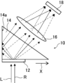
- FIG. 1 conceptually shows an example of the optical element of the present invention.
- the optical element 10 shown in FIG. 1 includes a liquid crystal diffraction element 12 and a prism 14.
- the liquid crystal diffraction element 12 has an optically anisotropic layer (numeral 26 in FIG. 2).
- the optically anisotropic layer has a liquid crystal alignment pattern in which the direction of an optical axis derived from a liquid crystal compound changes while continuously rotating along at least one in-plane direction.
- the optically anisotropic layer having such a liquid crystal alignment pattern that is, the liquid crystal diffraction element 12 having such an optically anisotropic layer, when unpolarized light is incident, spectrally spectra the incident light according to the wavelength.
- the right-handed circularly polarized light R right-handed circularly polarized light component R
- the left-handed circularly polarized light L left-handed circularly polarized light component L
- the liquid crystal diffraction element 12 diffracts the incident unpolarized light, separates the unpolarized light into right-handed circularly polarized light and left-handed circularly polarized light, and diffracts (refracts) the unpolarized light in the opposite direction.
- the liquid crystal diffraction element 12 is arranged on one surface of the prism 14.
- the surface on which this prism 14 is arranged is the first surface in the present invention.
- the liquid crystal diffraction element 12 diffracts right-handed circularly polarized light R toward the right in the figure and diffracts left-handed circularly polarized light L toward the left in the figure from among non-polarized incident light.
- the light diffracted to the left is reflected by the second surface 14a of the prism 14.
- the light diffracted in the right direction by the liquid crystal diffraction element 12 (left-handed circularly polarized light) and the light reflected by the second surface 14a of the prism 14 become parallel light and are emitted from the same surface of the prism 14 in the same direction. It is emitted. Note that the light reflected by the second surface 14a of the prism 14 is converted into left-handed circularly polarized light by reflection. Therefore, according to the present invention, the light separated by the liquid crystal diffraction element can be used with high utilization efficiency. The above points will be explained in detail later.
- FIG. 2 conceptually shows an example of a liquid crystal diffraction element.
- the illustrated liquid crystal diffraction element 12 includes a support 20, an alignment film 24, and an optically anisotropic layer 26.
- the optically anisotropic layer 26 is formed using a composition containing a liquid crystal compound 30.
- the optically anisotropic layer 26 has a predetermined liquid crystal alignment pattern in which the direction of the optical axis originating from the liquid crystal compound 30 changes continuously as it rotates along at least one direction.
- the liquid crystal diffraction element 12 has the support 20, the liquid crystal diffraction element does not need to have the support 20.
- the support body 20 may be peeled off from the structure shown in FIG. 2, and the liquid crystal diffraction element may be configured only with the alignment film 24 and the optically anisotropic layer 26.
- the support 20 and the alignment film 24 may be peeled off to form a liquid crystal diffraction element using only the optically anisotropic layer 26.
- the first surface of the prism 14, which will be described later, may act as a support.
- the liquid crystal diffraction element 12 has an optically anisotropic layer formed using a composition containing a liquid crystal compound, and the optically anisotropic layer has an optical axis derived from the liquid crystal compound.
- the liquid crystal alignment pattern has a liquid crystal alignment pattern in which the orientation of the liquid crystal changes while rotating continuously along at least one in-plane direction.
- the liquid crystal diffraction element 12 includes the support 20, the alignment film 24, and the optically anisotropic layer 26.
- the support body 20 supports the alignment film 24 and the optically anisotropic layer 26.
- the support 20 may be any of various sheet-like materials ( films, plates, layers) are available. Furthermore, the support may be flexible or non-flexible. Examples of the support include polyacrylic resin films such as polymethyl methacrylate, cellulose resin films such as cellulose triacetate, cycloolefin polymer films, resin films such as polyethylene terephthalate (PET), polycarbonate, and polyvinyl chloride; Additionally, a glass plate or the like can be used. Examples of the cycloolefin polymer film include "Arton” (trade name) manufactured by JSR Corporation and "Zeonor” (trade name) manufactured by Zeon Corporation.
- the thickness of the support 20 there is no limit to the thickness of the support 20, and the thickness that can hold the alignment film 24 and the optically anisotropic layer 26 can be determined as appropriate depending on the purpose of the liquid crystal diffraction element 12 and the material for forming the support 20. Just set it.
- Additives such as ultraviolet absorbers may be added to the support 20. It is preferable to add it to the support 20 as an ultraviolet absorber because it can improve the light resistance of the liquid crystal diffraction element 12.
- an alignment film 24 is formed on the surface of the support 20 .
- the alignment film 24 is an alignment film for aligning the liquid crystal compound 30 into a predetermined liquid crystal alignment pattern when forming the optically anisotropic layer 26 of the liquid crystal diffraction element 12.
- the optically anisotropic layer 26 has an optical axis 30A (see FIG. 3) originating from the liquid crystal compound 30 that is oriented along one in-plane direction (arrow X direction described later). It has a liquid crystal alignment pattern that changes as it rotates continuously. Therefore, the alignment film 24 of the liquid crystal diffraction element 12 is formed such that the optically anisotropic layer 26 can form this liquid crystal alignment pattern.
- the direction of the optical axis 30A is rotated is also simply referred to as "the optical axis 30A is rotated”.
- alignment films can be used as the alignment film 24.
- rubbed films made of organic compounds such as polymers, obliquely deposited films of inorganic compounds, films with microgrooves, and Langmuir films of organic compounds such as ⁇ -tricosanoic acid, dioctadecylmethylammonium chloride, and methyl stearate.
- Examples include a film in which LB (Langmuir-Blodgett) films are accumulated by the Blodgett method.
- the alignment film formed by rubbing treatment can be formed by rubbing the surface of the polymer layer several times in a certain direction with paper or cloth.
- Materials used for the alignment film include polyimide, polyvinyl alcohol, polymers having polymerizable groups described in JP-A-9-152509, JP-A-2005-97377, JP-A-2005-99228, and Preferred examples include materials used for forming alignment films and the like described in JP-A No. 2005-128503.
- a so-called photo-alignment film which is formed by irradiating a photo-alignable material with polarized or non-polarized light, is preferably used. That is, in the liquid crystal diffraction element 12, a photo-alignment film formed by applying a photo-alignment material on the support 20 is suitably used as the alignment film. Polarized light irradiation can be performed perpendicularly or obliquely to the photo-alignment film, and unpolarized light can be irradiated obliquely to the photo-alignment film.
- Examples of the photo-alignment material used in the photo-alignment film that can be used in the present invention include JP-A No. 2006-285197, JP-A No. 2007-76839, JP-A No. 2007-138138, and JP-A No. 2007-94071. Publication, JP 2007-121721, JP 2007-140465, JP 2007-156439, JP 2007-133184, JP 2009-109831, JP 3883848, and Patent No. Azo compounds described in JP-A No. 4151746, aromatic ester compounds described in JP-A No. 2002-229039, maleimides having photo-orientable units described in JP-A No. 2002-265541 and JP-A No.
- JP-A Preferable examples include photodimerizable compounds described in JP 2013-177561 and JP 2014-12823, particularly cinnamate compounds, chalcone compounds, and coumarin compounds.
- azo compounds, photocrosslinkable polyimides, photocrosslinkable polyamides, photocrosslinkable esters, cinnamate compounds, and chalcone compounds are preferably used.
- the thickness of the alignment film 24 is preferably 0.01 to 5 ⁇ m, more preferably 0.05 to 2 ⁇ m.
- the method for forming the alignment film there are no restrictions on the method for forming the alignment film, and various known methods can be used depending on the material for forming the alignment film.
- One example is a method in which an alignment film is applied to the surface of the support 20 and dried, and then the alignment film is exposed to laser light to form an alignment pattern.
- FIG. 7 conceptually shows an example of an exposure apparatus that exposes the alignment film 24 to form the above-mentioned alignment pattern.
- the exposure apparatus 60 shown in FIG. 7 includes a light source 64 including a laser 62, a beam splitter 68 that separates the laser beam M emitted by the laser 62 into two beams MA and MB, and two separated beams MA and MB. It includes mirrors 70A and 70B and ⁇ /4 plates 72A and 72B, which are respectively arranged on the optical path of the MB.
- the light source 64 emits linearly polarized light P 0 .
- the ⁇ /4 plate 72A converts linearly polarized light P 0 (ray MA) into right-handed circularly polarized light PR
- the ⁇ /4 plate 72B converts linearly polarized light P 0 (ray MB) into left-handed circularly polarized light PL .
- a support 20 having an alignment film 24 on which an alignment pattern has not yet been formed is placed in an exposure section, and two light beams MA and MB are made to intersect and interfere with each other on the alignment film 24, and the interference light is transmitted to the alignment film 24. irradiate and expose. Due to this interference, the polarization state of the light irradiated onto the alignment film 24 changes periodically in the form of interference fringes. As a result, an alignment pattern in which the alignment state periodically changes can be obtained in the alignment film 24. In the exposure device 60, the period of the alignment pattern can be adjusted by changing the intersection angle ⁇ of the two light beams MA and MB.
- the optical axis 30A derived from the liquid crystal compound 30 rotates in one direction.
- the length of one period in which the optical axis 30A rotates by 180 degrees can be adjusted.
- an optically anisotropic layer on an alignment film having an alignment pattern in which the alignment state changes periodically, the optical axis 30A originating from the liquid crystal compound 30 is oriented in one direction, as described later.
- An optically anisotropic layer 26 having a liquid crystal alignment pattern that rotates continuously can be formed. Further, by rotating the optical axes of the ⁇ /4 plates 72A and 72B by 90 degrees, the direction of rotation of the optical axis 30A can be reversed.
- the alignment film is provided as a preferred embodiment and is not an essential component.
- the optically anisotropic layer 26 and the like can be formed into the liquid crystal compound 30. It is also possible to configure a liquid crystal alignment pattern in which the direction of the originating optical axis 30A changes while continuously rotating along at least one in-plane direction.
- an optically anisotropic layer 26 is formed on the surface of the alignment film 24.
- the optically anisotropic layer 26 is composed of a liquid crystal compound 30 (liquid crystal compound molecules) on the surface of the alignment film. ) are shown.
- the optically anisotropic layer 26 has an oriented liquid crystal compound 30, similar to an optically anisotropic layer formed using a composition containing a normal liquid crystal compound. It has a stacked structure in the thickness direction.
- the optically anisotropic layer (liquid crystal layer) 26 is formed using a composition containing a liquid crystal compound.
- the optically anisotropic layer 26 functions as a general ⁇ /2 plate, that is, the mutually orthogonal light contained in the light incident on the optically anisotropic layer It has a function of giving a phase difference of half wavelength, that is, 180°, to two linearly polarized light components.
- the optically anisotropic layer 26 has a liquid crystal alignment pattern in which the direction of the optical axis 30A originating from the liquid crystal compound 30 changes while continuously rotating in one direction indicated by the arrow X in the plane.
- the optical axis 30A originating from the liquid crystal compound 30 is an axis in which the refractive index is the highest in the liquid crystal compound 30, that is, a so-called slow axis.
- the optical axis 30A is along the long axis direction of the rod shape.
- the optical axis 30A originating from the liquid crystal compound 30 is also referred to as “the optical axis 30A of the liquid crystal compound 30" or “the optical axis 30A.”
- the liquid crystal compounds 30 are two-dimensionally arranged in a plane parallel to the arrow X direction and the Y direction perpendicular to the arrow X direction. Note that in FIG. 2 and FIGS. 4 and 5, which will be described later, the Y direction is a direction perpendicular to the plane of the paper.
- FIG. 3 conceptually shows a plan view of the optically anisotropic layer 26.
- the main surface is the largest surface of the sheet-like object, and usually both sides of the sheet-like object in the thickness direction.
- the optically anisotropic layer 26 has a structure in which the liquid crystal compounds 30 are stacked from the liquid crystal compound 30 on the surface of the alignment film 24 as described above. It is as follows.
- the optically anisotropic layer 26 has a liquid crystal alignment pattern in which the direction of the optical axis 30A originating from the liquid crystal compound 30 changes while continuously rotating along the arrow X direction in the plane.
- the direction of the optical axis 30A of the liquid crystal compound 30 changing while rotating continuously in the arrow X direction means that the liquid crystal compound 30 is aligned along the arrow X direction.
- the angle formed by the optical axis 30A of 30 and the direction of the arrow X differs depending on the position in the direction of the arrow X, and the angle formed by the optical axis 30A and the direction of the arrow This means that the angle changes sequentially up to ⁇ -180°.
- the difference in angle between the optical axes 30A of the liquid crystal compounds 30 adjacent to each other in the direction of the arrow X is preferably 45° or less, more preferably 15° or less, and even more preferably a smaller angle. .
- the liquid crystal compound 30 that forms the optically anisotropic layer 26 is oriented in the Y direction perpendicular to the direction of the arrow Liquid crystal compounds 30 having the same values are arranged at regular intervals. In other words, in the liquid crystal compounds 30 forming the optically anisotropic layer 26, the angles formed by the direction of the optical axis 30A and the direction of the arrow X are equal in the liquid crystal compounds 30 arranged in the Y direction.
- the optical axis 30A of the liquid crystal compound 30 in the direction of the arrow X in which the direction of the optical axis 30A continuously rotates and changes within the plane is 180 degrees.
- the length (distance) of rotation be the length ⁇ of one period in the liquid crystal alignment pattern.
- the length ⁇ of one period is also referred to as one period ⁇ .
- one period ⁇ in the liquid crystal alignment pattern is defined by the distance from ⁇ until the angle between the optical axis 30A of the liquid crystal compound 30 and the arrow X direction becomes ⁇ +180°.
- the distance between the centers of two liquid crystal compounds 30 having the same angle with respect to the arrow X direction in the arrow X direction is one period ⁇ .
- the distance between the centers in the arrow X direction of two liquid crystal compounds 30 whose arrow X direction coincides with the optical axis 30A direction is one period ⁇ .
- the liquid crystal alignment pattern of the optically anisotropic layer repeats this one period ⁇ in the arrow X direction, that is, in one direction in which the direction of the optical axis 30A continuously rotates and changes.
- the liquid crystal compounds arranged in the Y direction have the same angle between the optical axis 30A and the arrow X direction (one direction in which the optical axis of the liquid crystal compound 30 rotates).
- a region F is defined as a region in which the liquid crystal compound 30 having the same angle between the optical axis 30A and the arrow X direction is arranged in the Y direction.
- the value of in-plane retardation (Re) in each region F is a half wavelength, that is, ⁇ /2.
- the refractive index difference due to the refractive index anisotropy of the region F in the optically anisotropic layer is the refractive index in the in-plane slow axis direction of the region F, and the refractive index in the direction perpendicular to the slow axis direction.
- the refractive index difference ⁇ n due to the refractive index anisotropy of the region F is the refractive index of the liquid crystal compound 30 in the direction of the optical axis 30A and the refractive index of the liquid crystal compound 30 in the direction perpendicular to the optical axis 30A in the plane of the region F. It is equal to the difference between the refractive index and the refractive index. That is, the refractive index difference ⁇ n is equal to the refractive index difference of the liquid crystal compound.
- the left-handed circularly polarized light L When the polarized light L is incident, the left-handed circularly polarized light L is given a phase difference of 180° by passing through the optically anisotropic layer 26, and the transmitted light is converted into right-handed circularly polarized light R. Furthermore, when the left-handed circularly polarized light L that has entered the optically anisotropic layer 26 passes through the optically anisotropic layer 26, the absolute phase changes depending on the direction of the optical axis 30A of each liquid crystal compound 30. At this time, since the direction of the optical axis 30A is changing while rotating along the direction of the arrow X, the amount of change in the absolute phase of the left-handed circularly polarized light L differs depending on the direction of the optical axis 30A.
- the liquid crystal alignment pattern formed in the optically anisotropic layer 26 is a periodic pattern in the direction of the arrow X
- the left-handed circularly polarized light L passing through the optically anisotropic layer 26 is , a periodic absolute phase Q1 is given in the direction of arrow X corresponding to the direction of each optical axis 30A.
- an equiphase surface E1 tilted in a direction opposite to the direction of the arrow X is formed.
- the right-handed circularly polarized light R that passes through the optically anisotropic layer 26 is refracted so as to be inclined in a direction perpendicular to the equiphase plane E1, which is different from the traveling direction of the left-handed circularly polarized light L that is the incident light. proceed in the direction.
- the left-handed circularly polarized light L that has entered the optically anisotropic layer 26 is converted into right-handed circularly polarized light R that is tilted by a certain angle in the direction of the arrow X with respect to the incident direction.
- the amount of change in the absolute phase of the right-handed circularly polarized light R differs depending on the direction of the optical axis 30A. Furthermore, since the liquid crystal alignment pattern formed in the optically anisotropic layer 26 is a periodic pattern in the direction of the arrow X, the right-handed circularly polarized light R passing through the optically anisotropic layer 26 is , a periodic absolute phase Q2 is given in the direction of arrow X corresponding to the direction of each optical axis 30A.
- the incident light is right-handed circularly polarized light R
- the periodic absolute phase Q2 in the direction of arrow X corresponding to the direction of the optical axis 30A is opposite to that of left-handed circularly polarized light L shown in FIG.
- an equal phase plane E2 tilted in the direction of the arrow X which is opposite to that in the left-handed circularly polarized light L, is formed. Therefore, the right-handed circularly polarized light R is refracted so as to be inclined in a direction perpendicular to the equiphase plane E2, and travels in a direction different from the traveling direction of the right-handed circularly polarized light R.
- the right-handed circularly polarized light R that has entered the optically anisotropic layer 26 is converted into left-handed circularly polarized light L that is tilted by a certain angle in the direction opposite to the direction of the arrow X with respect to the incident direction.
- the direction of diffraction of transmitted light can be reversed. That is, in the examples shown in FIGS. 2 to 5, the rotation direction of the optical axis 30A in the direction of arrow X is clockwise.
- the optical axis 30A is rotated counterclockwise, when the incident light is left-handed circularly polarized light L, the transmitted light, right-handed circularly polarized light R, is rotated in the opposite direction to the arrow X direction.
- the incident light is right-handed circularly polarized light R, left-handed circularly polarized light L, which is transmitted light, is diffracted in the direction of arrow X.
- the in-plane retardation value of the plurality of regions F is preferably a half wavelength.
- ⁇ n ⁇ is the refractive index difference due to the refractive index anisotropy of the region F when the wavelength of the incident light is ⁇ nm
- d is the thickness of the optically anisotropic layer 26.
- the in-plane retardation values of the plurality of regions F in the optically anisotropic layer 26 can also be used outside the range of the above formula (1). Specifically, by setting ⁇ n ⁇ ⁇ d ⁇ 0.7 ⁇ ( ⁇ /2) nm or 1.3 ⁇ ( ⁇ /2) ⁇ ⁇ n ⁇ ⁇ d, the light is transmitted in the same direction as the traveling direction of the incident light. It can be divided into light that travels and light that travels in a direction different from the direction of travel of the incident light. When ⁇ n ⁇ ⁇ d approaches 0 nm or ⁇ nm, the component of light traveling in the same direction as the traveling direction of the incident light increases, and the component of light traveling in a direction different from the traveling direction of the incident light decreases.
- the angle of diffraction of the transmitted light can be adjusted. Specifically, the shorter one period ⁇ of the liquid crystal alignment pattern, the stronger the light that has passed through the liquid crystal compounds 30 adjacent to each other interferes with each other, so that the transmitted light can be diffracted to a greater extent. That is, when light is incident from the normal direction of the optically anisotropic layer 26, the shorter one period ⁇ of the liquid crystal alignment pattern, the larger the angle between the normal direction and the transmitted light (diffraction light).
- the normal direction is a direction perpendicular to a plane such as the main surface of the sheet-like object.
- the optically anisotropic layer 26 can diffract transmitted light to a greater extent as the wavelength of incident light is longer. That is, when light is incident from the normal direction of the optically anisotropic layer 26, the longer the wavelength of the incident light, the larger the angle of the transmitted light (diffracted light) with respect to the normal direction. Therefore, the optically anisotropic layer 26 (liquid crystal diffraction element 12) can separate incident light into wavelengths. For example, when white light is incident on the optically anisotropic layer 26 from the normal direction, the angle between the normal direction and the transmitted light is the largest for red light, the second largest for green light, and the angle between the normal direction and the transmitted light for blue light. is the smallest, so this allows white light to be split into red, green, and blue light.
- the angle of diffraction by the optically anisotropic layer 26 is determined by " ⁇ / ⁇ " depending on one period ⁇ and the wavelength ⁇ of the incident light.
- the angle of diffraction (refraction) is the same whether the incident light is right-handed circularly polarized light R or left-handed circularly polarized light L.
- the angle between the transmitted right-handed circularly polarized light R and the normal direction, and the angle between the transmitted left-handed circularly polarized light L and the The angles formed by the line direction are equal.
- the optically anisotropic layer 26 is formed by curing a liquid crystal composition containing a rod-like liquid crystal compound or a discotic liquid crystal compound, and the optical axis of the rod-like liquid crystal compound or the optical axis of the discotic liquid crystal compound is as described above. It has an oriented liquid crystal alignment pattern.
- an alignment film 24 By forming an alignment film 24 on the support 20, applying a liquid crystal composition onto the alignment film 24, and curing it, an optically anisotropic layer 26 made of a cured layer of the liquid crystal composition can be obtained.
- the optically anisotropic layer 26 that functions as a so-called ⁇ /2 plate
- the present invention provides an embodiment in which a laminate integrally provided with the support 20 and the alignment film 24 functions as a ⁇ /2 plate. including.
- the liquid crystal composition for forming the optically anisotropic layer 26 contains a rod-like liquid crystal compound or a disk-like liquid crystal compound, and further contains other substances such as a leveling agent, an alignment control agent, a polymerization initiator, and an alignment aid. It may contain ingredients.
- the optically anisotropic layer 26 preferably has a wide band with respect to the wavelength of the incident light, and is preferably constructed using a liquid crystal material whose birefringence index is inverse dispersion. It is also preferable to make the optically anisotropic layer substantially broadband with respect to the wavelength of incident light by imparting a torsion component to the liquid crystal composition and/or by stacking different retardation plates. .
- Japanese Patent Laid-Open No. 2014-089476 discloses a method of realizing a broadband patterned ⁇ /2 plate by laminating two layers of liquid crystals with different twist directions in an optically anisotropic layer. , can be preferably used in the present invention.
- -Rod-shaped liquid crystal compound- Rod-shaped liquid crystal compounds include azomethines, azoxys, cyanobiphenyls, cyanophenyl esters, benzoic acid esters, cyclohexanecarboxylic acid phenyl esters, cyanophenylcyclohexanes, cyano-substituted phenylpyrimidines, alkoxy-substituted phenylpyrimidines, Phenyldioxanes, tolans and alkenylcyclohexylbenzonitrile are preferably used.
- high-molecular liquid crystal molecules can also be used.
- the polymerizable rod-like liquid crystal compound examples include Makromol. Chem. , vol. 190, p. 2255 (1989), Advanced Materials vol. 5, p. 107 (1993), US Pat. No. 4,683,327, US Pat. No. 5,622,648, US Pat. 95/24455, 97/00600, 98/23580, 98/52905, JP 1-272551, 6-16616, 7-110469, 11-80081 Compounds described in Japanese Patent Application No. 2001-64627 and the like can be used. Further, as the rod-shaped liquid crystal compound, for example, those described in Japanese Patent Publication No. 11-513019 and Japanese Patent Application Laid-open No. 2007-279688 can also be preferably used.
- the discotic liquid crystal compound for example, those described in JP-A No. 2007-108732 and JP-A No. 2010-244038 can be preferably used.
- the liquid crystal compound 30 stands up in the thickness direction in the optically anisotropic layer, and the optical axis 30A originating from the liquid crystal compound is aligned with the disc surface. It is defined as an axis perpendicular to , the so-called fast axis (see FIG. 25).
- the thickness of the optically anisotropic layer 26 it is preferably 20 ⁇ m or less, more preferably 15 ⁇ m or less, and even more preferably 10 ⁇ m or less. Particularly preferred is 5 ⁇ m or less.
- the optical axis 30A of the liquid crystal compound 30 constituting the optically anisotropic layer 26 is aligned in the thickness direction.
- the present invention is not limited to this, and in the optical element 10 of the present invention, as conceptually shown in FIG. A spirally twisted orientation along the thickness direction of layer 26 is preferred.
- the liquid crystal compound 30 constituting the optically anisotropic layer 26 is twisted and oriented in a spiral shape along the thickness direction, the diffraction efficiency of right-handed circularly polarized light and left-handed circularly polarized light increases depending on the twist direction of the spiral. It will be different. Therefore, when the liquid crystal compound 30 constituting the optically anisotropic layer 26 is twisted and oriented in a spiral manner along the thickness direction, as shown in FIG. It is preferable to laminate two layers of 26.
- the diffraction efficiency of both right-handed circularly polarized light and left-handed circularly polarized light can be improved, and the diffraction efficiency of right-handed circularly polarized light and left-handed circularly polarized light can be matched.
- the number of optically anisotropic layers stacked is not limited to one or two layers, and may be three or more layers as necessary.
- the twist angle of the liquid crystal compound 30 in the optically anisotropic layer 26.
- the absolute value of the twist angle of the liquid crystal compound 30 is 5 to 360 in order to suitably improve the diffraction efficiency.
- the angle is preferably 10° to 320°, more preferably 20° to 280°, particularly preferably 30° to 250°.
- the twist angle of the liquid crystal compound 30 is the twist angle of the liquid crystal compound 30 twisted and oriented in the thickness direction in the optically anisotropic layer 26 from the bottom surface to the top surface.
- the liquid crystal diffraction element 12 having such an optically anisotropic layer 26 is arranged on one surface of the prism 14.
- the liquid crystal diffraction element 12 has the alignment film 24 and/or the support body 20
- the liquid crystal diffraction element 12 has the optically anisotropic layer 26 on the prism 14 side even if the optically anisotropic layer 26 is on the prism 14 side.
- 14 may be placed on the opposite side.
- an antireflection film such as a dielectric multilayer film or a moth-eye film may be provided at the interface with air.
- the liquid crystal diffraction element 12 can be directly attached to the prism 14 by using the prism 14 as the support 20 shown in FIG. They may be placed adjacent to each other. Furthermore, the liquid crystal diffraction element 12 may be provided in direct contact with one surface of the prism 14 by methods such as alignment treatment, application of a liquid crystal composition, and polymerization. Alternatively, the liquid crystal diffraction element 12 may be attached to one surface of the prism 14 using an adhesive such as an optically clear adhesive (OCA), an optically transparent double-sided tape, or an ultraviolet curing resin. Good too. Alternatively, the liquid crystal diffraction element 12 may be bonded directly to one surface of the prism 14 by performing surface treatment to enhance adhesion such as plasma treatment. If necessary, an antireflection film or the like may be provided between the prism 14 and the liquid crystal diffraction element 12.
- OCA optically clear adhesive
- an antireflection film or the like may be provided between the prism 14 and the liquid crystal diffraction element 12.
- this layer is an optically anisotropic layer.
- it has a refractive index similar to that of the optical layer 26 and the prism 14. That is, it is preferable that the optically anisotropic layer 26 and the prism 14 are in close optical contact.
- the difference in refractive index between this layer and the optically anisotropic layer 26 and the prism 14 is ⁇ It is preferably 0.5 or less, more preferably ⁇ 0.3 or less.
- the prism 14 is a triangular prism having a right triangular bottom surface.
- the liquid crystal diffraction element 12 is arranged on the sides of a right triangle that sandwich the right angle.
- the surface on which the prism 14 is arranged is the first surface of the prism in the present invention, and the surfaces that are the sides that sandwich the right angle of the right triangle together with this first surface are the surfaces that cause diffraction by the liquid crystal diffraction element 12. This becomes the second surface that reflects the light separated by.
- the light separated by diffraction by the liquid crystal diffraction element 12 is right-handed circularly polarized light or left-handed circularly polarized light.
- a prism is an optical member (optical element) made of a material such as quartz glass or crystal, that is, a transparent medium, for dispersing, refracting, total reflection, birefringence, etc. of light.
- light includes not only visible light but also electromagnetic waves such as the above-mentioned ultraviolet rays and infrared rays.
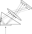
- the incident light is separated by diffraction by the liquid crystal diffraction element 12, as conceptually shown in FIG.
- the component of polarized light R is diffracted, for example, in the direction of arrow X (to the right in the figure), and the component of left-handed circularly polarized light L is diffracted in the opposite direction to the direction of arrow X (to the left in the figure).
- the rotating direction of the transmitted light is opposite to that of the incident light.
- the light separated by the liquid crystal diffraction element 12 and diffracted to the left in the figure propagates within the prism 14 and enters the second surface 14a orthogonal to the first surface of the prism 14 on which the liquid crystal diffraction element 12 is arranged. and is reflected specularly. Note that due to this reflection, the rotation direction of the circularly polarized light is reversed.
- the angle of diffraction by the liquid crystal diffraction element 12 is the same regardless of the wavelength of the light. Therefore, the light ( The diffracted light) and the light diffracted by the optically anisotropic layer 26 in the opposite direction to the light incident on the second surface 14a (diffracted light) become parallel light.
- the two lights separated by the liquid crystal diffraction element 12 according to the rotation direction of the circularly polarized light become parallel lights, and both are emitted from a surface other than the first surface and the second surface 14a of the prism 14. .
- this surface will also be referred to as the third surface for convenience.
- the light diffracted by the liquid crystal diffraction element 12 is shown as two separated beams of the same wavelength in order to simply illustrate the function of the optical element 10.
- the incident light that has entered the optical element 10 of the present invention is split into a plurality of lights by the liquid crystal diffraction element 12 and diffracted at an angle depending on the wavelength.
- the incident light may be short wavelength light (monochromatic light).
- the light emitted from the third surface of the prism 14 is shown to travel straight through the third surface and pass through it.
- the light emitted from the third surface depends on the difference in refractive index between the material forming the prism 14 and air, and the angle of incidence on the third surface. It is refracted at the interface and exits. Regarding this point, the same applies to other figures for explaining the optical element of the present invention.
- the light diffracted by the liquid crystal diffraction element 12 (optically anisotropic layer 26) is separated according to the rotation direction of the circularly polarized light, and is separated in the opposite direction, that is, in the arrow X direction and in the arrow X direction. is diffracted in the opposite direction. Therefore, it is difficult to use both of the lights that have been diffracted by the liquid crystal diffraction element 12 and separated into two, and in many cases only one of them can be used. That is, optical elements using conventional liquid crystal diffraction elements have low utilization efficiency of separated light.
- optical elements such as spectroscopic elements become larger and more complex.
- the two lights separated by the diffraction of the liquid crystal diffraction element 12 are emitted as parallel lights from the same surface (third surface) of the prism 14. That is, according to the optical element 10 of the present invention, the two lights separated by the diffraction of the liquid crystal diffraction element 12 are emitted from the same surface (third surface) of the prism 14 in the same direction.
- the liquid crystal diffraction element 12 separates the incident light, but as described above, the liquid crystal diffraction element 12 diffracts right-handed circularly polarized light and left-handed circularly polarized light, although the diffraction directions are opposite. , if the wavelengths are the same, the diffraction angles are the same. Therefore, as shown in FIG. 9 by solid lines, broken lines, and dashed-dotted lines, one of the separated lights is diffracted in the direction of arrow X (to the right in the figure), and the other is specularly reflected by the second surface of the prism 14.
- the two lights that are separated and separated by diffraction by the liquid crystal diffraction element 12 become parallel lights and exit from the third surface of the prism 14 .
- the broken line is, for example, blue light
- the solid line is, for example, green light
- the dashed line is, for example, red light.
- the optical element 10 of the present invention two lights (diffraction lights) separated by the liquid crystal diffraction element 12 can be easily utilized.
- the utilization efficiency of the light separated by the liquid crystal diffraction element 12 can be improved.
- the lens 16 is placed facing the third surface of the prism 14 to focus the light, the parallel light will be focused at the same position, so it will be easier to move the liquid crystal diffraction element 12
- the two separated lights can be photometered by one detector 18. That is, according to the present invention, the utilization efficiency of the light separated by the liquid crystal diffraction element 12 can be improved. Further, as shown in FIG.
- the optical element 10 of the present invention has a simple and compact configuration in which the optical element 10 is combined with one lens 16 and one detector 18, and can be used, for example, in a spectrometer. Can be configured. That is, according to the optical element 10 of the present invention, it is possible to downsize the optical system.
- the material for forming the prism 14 is not limited, and all of the various materials used for various prisms can be used.
- the difference in refractive index between the prism 14 and the liquid crystal diffraction element 12 is small.
- the refractive index difference between the prism 14 and the liquid crystal diffraction element 12 is preferably ⁇ 0.5 or less, more preferably ⁇ 0.3 or less.
- the second surface 14a of the prism 14 that is, the surface of the prism 14 that reflects one of the lights separated by the liquid crystal diffraction element 12, totally reflects this light. That is, it is preferable that the liquid crystal diffraction element 12 diffracts the incident light so that one of the separated lights is incident on the second surface 14a of the prism 14 at an angle equal to or greater than the critical angle.
- the angle of diffraction of circularly polarized light by the liquid crystal diffraction element 12 is determined by " ⁇ / ⁇ " depending on one period ⁇ of the optically anisotropic layer 26 and the wavelength ⁇ of the incident light. Therefore, in the optical element 10 of the present invention, the optical anisotropy is adjusted so that the incident angle of the light incident on the second surface 14a of the prism 14 is equal to or greater than the critical angle, depending on the wavelength of the light to be subjected to spectroscopy. Preferably, one period ⁇ of layer 26 is determined. Furthermore, if the angle of incidence of light incident on the second surface 14a is too large, the size of the prism 14 will become large.
- one period ⁇ it is also preferable to determine one period ⁇ so that the angle of incidence of light incident on the second surface 14a does not become large and the size of the prism 14 does not become large.
- the wavelength ⁇ of the light to be subjected to spectroscopy is 450 nm
- one period ⁇ is 0.3 to 2 ⁇ m.
- the wavelength ⁇ of the light to be analyzed is 550 nm
- one period ⁇ is 0.4 to 3 ⁇ m.
- the wavelength ⁇ of the light to be subjected to spectroscopy is 700 nm, it is preferable that one period ⁇ is 0.5 to 4 ⁇ m.
- the wavelength ⁇ of the light to be subjected to spectroscopy is 1000 nm
- one period ⁇ is 0.8 to 5 ⁇ m.
- the incident light that enters the optical element 10 of the present invention is from the normal direction of the liquid crystal diffraction element 12, but the present invention is not limited to this. That is, the light may be incident on the optical element 10 (liquid crystal diffraction element 12) of the present invention from a direction having an angle with respect to the normal direction of the liquid crystal diffraction element 12. Therefore, in this case, in addition to the wavelength of the light to be separated, the optical system is adjusted so that the angle of incidence of the light on the second surface 14a of the prism 14 is equal to or less than the critical angle, depending on the set angle of incidence of the incident light. Preferably, one period ⁇ of the anisotropic layer 26 is determined. Alternatively, the angle of incidence of light on the optical element 10 (liquid crystal diffraction element 12) of the present invention may be adjusted so that the angle of incidence of light on the second surface 14a of the prism 14 is equal to or less than the critical angle.
- the second surface 14a of the prism 14 is not limited to total reflection of light.
- light may be regularly reflected on the second surface 14a of the prism 14 by providing a reflective film such as a dielectric multilayer film or a metal film on the second surface 14a of the prism 14.
- a reflective film such as a dielectric multilayer film or a metal film on the second surface 14a of the prism 14.
- the utilization efficiency of the light separated by the liquid crystal diffraction element 12 by making one of the lights separated by the liquid crystal diffraction element 12 incident at an angle equal to or greater than the critical angle, all of the light is absorbed by the second surface 14a of the prism 14.
- Preferably reflective is preferferably reflective.
- the illustrated optical element 10 has a prism 14 having a first surface on which the liquid crystal diffraction element 12 is disposed, and a second surface 14a that reflects one of the lights diffracted and separated by the liquid crystal diffraction element 12. are orthogonal. More specifically, in the optical element 10, the main surface of the liquid crystal diffraction element 12 (optically anisotropic layer 26) and the second surface of the prism 14 are perpendicular to each other. However, in the optical element of the present invention, the angle between the first surface (principal surface of the liquid crystal diffraction element 12) and the second surface of the prism 14 may be in various forms other than orthogonal.
- the incident angle (incidence direction) of the light deviates from the normal direction of the first surface of the prism 14, the same effect can be obtained by deviating the angle between the first surface and the second surface 14a from orthogonal.
- the effect of making one diffracted light from the first surface and the other diffracted light from the first surface reflected by the second surface 14a parallel to each other can be obtained.
- one direction in which the optical axis rotates in the optically anisotropic layer 26 (arrow X direction) is parallel to the direction of the diffraction vector of the second surface 14a, that is, the direction in which the periodic structure of the diffraction element repeats. is preferred.
- the normal direction of the second surface 14a and the direction of arrow X are parallel. Further, it is preferable that the direction of the arrow X is included within a plane perpendicular to the first surface and the second surface 14a. Furthermore, it is desirable that the line (ridge line) formed by the angle between the first surface and the second surface 14a of the prism 14 be orthogonal to the direction of the arrow X.
- the angle formed between the first surface and the second surface of the prism 14 may be an obtuse angle, as in the optical element 10A conceptually shown in FIG.
- the light travels in the direction of separation and is emitted from the third surface.
- This optical element as conceptually shown in FIG.
- the intensity of the light separated into right-handed circularly polarized light R and left-handed circularly polarized light L can be measured using the instrument 18.
- the angle formed between the first surface and the second surface of the prism 14 may be an acute angle.
- the light diffracted by the liquid crystal diffraction element 12 in the direction of arrow X (rightward) and the light diffracted in the opposite direction and reflected by the second surface 14a of the prism 14 are brought close to each other. The light travels in the direction and is emitted from the third surface (see FIG. 14).
- the angle between the first surface (principal surface of the liquid crystal diffraction element 12) and the second surface of the prism 14 is preferably 70 to 110 degrees, more preferably 80 to 110 degrees, and even more preferably 90 degrees.
- the angle between the first and second surfaces of the prism 14 is preferably 70 to 110 degrees, it is possible to more reliably improve the utilization efficiency of the separated light, and to detect the spectroscopy of light according to the polarization in a close range. It is preferable because it can be done.
- the liquid crystal diffraction element 12 is basically arranged parallel to the first surface of the prism 14. Therefore, in the above explanation, the angle formed between the first surface and the second surface 14a of the prism 14 is explained, but the most important point is that the main surface and the second surface 14a of the liquid crystal diffraction element 12 (optically anisotropic layer 26) is the angle formed by
- both of the two lights separated by the liquid crystal diffraction element 12 are emitted from the third surface of the prism 14. Therefore, the angle formed by the first and second surfaces 14a and the third surface is appropriately set so that the light incident on the third surface can be emitted without being reflected.
- the first surface and The angle between the prism 14 and the third surface, which is the light exit surface is preferably 5 to 60 degrees, more preferably 10 to 45 degrees.
- a retardation layer 19 is provided on the surface of the prism 14 that reflects one of the lights separated by the liquid crystal diffraction element 12, as in the optical element 10B conceptually shown in FIG. It's okay.
- the prism 14 has a retardation layer 19, one of the lights separated by the liquid crystal diffraction element 12 is reflected after having its phase adjusted by the retardation layer 19.
- the retardation layer 19 There is no limit to the retardation layer 19, and various known retardation layers can be used. Furthermore, there is no limit to the retardation provided by the retardation layer 19. Note that in order to prevent reflection at the interface between the prism 14 and the retardation layer 19, it is preferable that the prism 14 and the retardation layer 19 have similar refractive indexes. Specifically, the difference in refractive index between the prism 14 and the retardation layer 19 is preferably ⁇ 0.5 or less, more preferably ⁇ 0.3 or less.
- the prism 14 is a triangular prism, and the light separated by the liquid crystal diffraction element 12 disposed on the first surface is reflected by one side directly and the other by the second surface 14a. , the light is emitted from a third surface different from the first surface and the second surface 14a.
- the present invention is not limited to this.
- the two lights are separated by one or more surfaces of the prism. may be reflected, and two lights (diffraction lights) may be emitted from the first surface where the liquid crystal diffraction element 12 is arranged, other than the area where the liquid crystal diffraction element is arranged.
- one of the lights separated by the liquid crystal diffraction element 12 and the light reflected by the second surface are made parallel, and then the two lights are reflected by one or more surfaces of the prism, and the light is produced for the first time in the prism. Two lights (diffraction lights) may be emitted from the incident surface.
- the two lights separated by the liquid crystal diffraction element 12 are made parallel, the two lights are reflected on the same surface.
- Various configurations can be used for the propagation of light within the prism. However, whatever the configuration, it is preferable that the two lights separated by the liquid crystal diffraction element 12 be emitted from the same surface of the prism.
- Example 1 ⁇ Preparation of liquid crystal diffraction element> (Formation of alignment film)
- a glass substrate manufactured by Corning, EAGLE
- the following coating solution for forming an alignment film was applied onto the support by spin coating.
- the support on which the coating film of the coating liquid for forming an alignment film was formed was dried on a hot plate at 60° C. for 60 seconds to form an alignment film.
- Coating liquid for forming alignment film ⁇
- the following photo-alignment material 1.00 parts by mass ⁇ Water 16.00 parts by mass ⁇ Butoxyethanol 42.00 parts by mass ⁇ Propylene glycol monomethyl ether 42.00 parts by mass ⁇ ⁇
- the alignment film was exposed by irradiating the formed alignment film with polarized ultraviolet light (50 mJ/cm 2 , using an ultra-high pressure mercury lamp).
- the alignment film was exposed using the exposure apparatus shown in FIG. 7 to form an alignment film having an alignment pattern.
- a laser that emits a laser beam having a wavelength (325 nm) was used.
- the exposure amount by interference light was 300 mJ/cm 2 .
- the intersecting angle (intersecting angle ⁇ ) of the two laser beams was adjusted so that one period ⁇ (length of rotation of the optical axis by 180°) of the alignment pattern formed by the interference of the two laser beams was 1 ⁇ m. did.
- composition B-1 (Formation of optically anisotropic layer (liquid crystal layer))
- the following composition B-1 was prepared as a liquid crystal composition for forming an optically anisotropic layer.
- Rod-shaped liquid crystal compound L-1 (contains the following structure in the mass ratio shown on the right)
- the optically anisotropic layer was formed by applying composition B-1 in multiple layers on the alignment film. Specifically, the first layer of composition B-1 is coated on the alignment film, heated, cooled, and then cured with ultraviolet rays to create a liquid crystal fixing layer. The coating was repeated in layers, followed by heating, cooling, and then UV curing.
- composition B-1 was applied onto the alignment film, and the coating film was heated to 80° C. on a hot plate. Thereafter, the orientation of the liquid crystal compound was fixed by irradiating the coating film with ultraviolet light having a wavelength of 365 nm at a dose of 300 mJ/cm 2 using a high-pressure mercury lamp in a nitrogen atmosphere at 80°C.
- this liquid crystal fixing layer was overcoated, heated under the same conditions as above, and after cooling, ultraviolet curing was performed to produce a liquid crystal fixing layer. In this way, overcoating was repeated until the total thickness reached the desired thickness to form an optically anisotropic layer.
- the refractive index difference ⁇ n of the cured layer of Composition B-1 is determined by coating Composition B-1 on a separately prepared support with an alignment film for retardation measurement, and making sure that the director of the liquid crystal compound is parallel to the substrate.
- the retardation Re ( ⁇ ) and film thickness of the liquid crystal fixed layer obtained by aligning the liquid crystal so as to have the following properties and then fixing it by irradiating ultraviolet rays were determined.
- ⁇ n ⁇ can be calculated by dividing the retardation Re( ⁇ ) by the film thickness.
- the retardation Re ( ⁇ ) was measured at a desired wavelength using Axoscan from Axometrix, and the film thickness was measured using a SEM (Scanning Electron Microscope).
- the refractive index ne ( ⁇ ) for extraordinary light and the refractive index no ( ⁇ ) for ordinary light were measured using an Abbe refractometer. Further, the refractive index difference ⁇ n( ⁇ ) was determined from the difference between ne( ⁇ ) and no( ⁇ ). In the expressions Re( ⁇ ), ne( ⁇ ), no( ⁇ ), and ⁇ n( ⁇ ), ⁇ is the wavelength of the incident light. In the following, the wavelength ⁇ of the incident light was 633 nm.
- the formed optically anisotropic layer was transferred and bonded to the bottom surface of the prepared triangular prism.
- This triangular prism is made of optical glass with model number SK2 manufactured by SCHOTT, and has a refractive index of 1.605 at a wavelength of 633 nm.
- the prepared triangular prism has one angle of 90°. Further, the angle of the slope (hytenuse side) of the triangular prism is 20°.
- the optically anisotropic layer was bonded to the surface sandwiched between the right angle and the 20° angle of the triangular prism. The bonding was performed by direct bonding using plasma treatment to enhance adhesion.
- the lamination direction of the optically anisotropic layer is the direction in which the direction of the optical axis of the liquid crystal compound in the optically anisotropic layer changes while rotating, that is, the direction of the diffraction vector in the plane of the optically anisotropic layer (bright and dark lines). (direction perpendicular to the prism) is made to be perpendicular to the direction of the straight line formed by the right angle of the triangular prism. In this way, an optical element was produced.
- composition B-2 was prepared in order to form a first optically anisotropic layer in which a liquid crystal compound was oriented in a right-handed spiral in the thickness direction.
- Composition B-2 ⁇ - Rod-shaped liquid crystal compound L-1 100.00 parts by mass - Chiral agent Ch-A 0.23 parts by mass - Polymerization initiator (manufactured by BASF, Irgacure (registered trademark) 907) 3.00 parts by mass photosensitizer (Nippon Kayaku, KAYACURE DETX-S) 1.00 parts by mass ⁇ Leveling agent T-1 0.08 parts by mass ⁇ Methyl ethyl ketone 2000.00 parts by mass ⁇ ⁇
- a first optically anisotropic layer was formed on the alignment film by applying multiple layers of composition B-2 in the same manner as in Example 1 (composition B-1).
- the twist angle in the thickness direction of the liquid crystal compound was 70° (right twist).
- diagonal bright and dark lines were observed with respect to the lower interface of the optically anisotropic layer (interface with the support). These diagonal bright and dark lines are observed due to the structure in which the liquid crystal compound is twisted and oriented in a spiral shape in the thickness direction.
- composition B-3 Liquid crystal compound L-1 100.00 parts by mass Chiral agent Ch-B 0.39 parts by mass Polymerization initiator (manufactured by BASF, Irgacure (registered trademark) 907) 3.00 parts by mass photosensitizer (Nippon Kayaku, KAYACURE DETX-S) 1.00 parts by mass Leveling agent T-1 0.08 parts by mass Methyl ethyl ketone 2000.00 parts by mass ⁇ ⁇
- a second optically anisotropic layer was formed on the first optically anisotropic layer in the same manner as the first optically anisotropic layer except that Composition B-3 was used.
- An optical element was produced in the same manner as in Example 1 using the produced two optically anisotropic layers.
- Example 3 As triangular prisms, triangular prisms having apex angles of 80°, 20°, and 80° were prepared. This triangular prism is made of optical glass with model number SK2 manufactured by SCHOTT, and has a refractive index of 1.605 at a wavelength of 633 nm. The 90° angle in Example 1 was replaced with an 80° corner, and the optically anisotropic layer prepared in Example 2 was placed on the surface sandwiched between the 80° corner and the 20° corner of this triangular prism. An optical element was produced by bonding in the same manner as in Example 1.
- each angle is shown in the table below.
- the spectroscopic system was constructed in such a way that a line (image) sensor captures signals collected by a condensing lens for each wavelength after the exit surface.
- a line (image) sensor captures signals collected by a condensing lens for each wavelength after the exit surface.
- light of 550 nm could be analyzed with high efficiency of 95% or more.
- spectroscopy was possible with high efficiency of 50% or more at 400 nm and 700 nm, and 20% or more at 1000 nm.
- the ⁇ 1st-order light separated into the left and right by the diffraction element that is, the two diffracted lights separated in different directions depending on the polarization, are focused at different focal positions. is completed. That is, it can be seen that by using the optical element of Example 3, it functions as a polarization spectroscopy system that can perform spectroscopy according to polarization.
Abstract
The present invention addresses the problem of providing an optical element with which the utilization efficiency of spectral light can be improved. The problem is solved by having a liquid crystal diffraction element and a prism having a first surface that is in contact with the liquid crystal diffraction element directly or via another layer, wherein: the liquid crystal diffraction element includes an optically anisotropic layer having a liquid crystal alignment pattern in which the direction of an optical axis derived from a liquid crystal compound is changing while continuously rotating along at least one direction in a plane; and the prism has a second surface that reflects one of light beams separated due to the diffraction by the liquid crystal diffraction element.
Description
本発明は、液晶回折素子によって入射光を分光する光学素子に関する。
The present invention relates to an optical element that spectrally separates incident light using a liquid crystal diffraction element.
入射光を回折して透過する液晶回折素子が知られている。
このような液晶回折素子として、液晶化合物を含む液晶組成物を用いて形成された光学異方性層を有する液晶回折素子が知られている。 Liquid crystal diffraction elements that diffract and transmit incident light are known.
As such a liquid crystal diffraction element, a liquid crystal diffraction element having an optically anisotropic layer formed using a liquid crystal composition containing a liquid crystal compound is known.
例えば、特許文献1には、ブラッグ条件にしたがって、内部を通過する光の伝播の方向を変更するように構成されている液晶副層等の複数の積層複屈折副層を備え、この積層複屈折副層が、それぞれの格子周期を画定するように、積層複屈折副層の隣接するものの間のそれぞれの境界面に沿って変化する局所光軸を備える液晶回折素子(光学素子)が記載されている。
この液晶回折素子において、積層複屈折副層を構成する複屈折副層は、引用文献1の図2等に示されるように、棒状液晶化合物の向き、すなわち液晶化合物に由来する光学軸の向きが、一方向に向かって連続的に回転する液晶化合物の配向パターンを有する。 For example, US Pat. A liquid crystal diffractive element (optical element) is described with a local optical axis that varies along each interface between adjacent ones of the stacked birefringent sublayers such that the sublayers define respective lattice periods. There is.
In this liquid crystal diffraction element, the birefringent sublayer constituting the laminated birefringent sublayer is arranged so that the direction of the rod-shaped liquid crystal compound, that is, the direction of the optical axis derived from the liquid crystal compound, is , has an alignment pattern of liquid crystal compounds that rotates continuously in one direction.
特許文献1に記載されるような液晶化合物の配向パターン(液晶配向パターン)を有する液晶回折素子は、入射した光を、波長に応じた角度で回折(屈折)できる。また、同じ波長の光であれば、一定の角度で光を回折できる。
液晶配向パターンを有する液晶回折素子は、このような特性を利用して、各種の用途に利用可能である。例えば、この液晶回折素子は、入射光を多数の波長域に分光して撮影する、ハイパースペクトルカメラにおける分光素子として、好適に利用可能である。 A liquid crystal diffraction element having an orientation pattern of a liquid crystal compound (liquid crystal orientation pattern) as described inPatent Document 1 can diffract (refract) incident light at an angle depending on the wavelength. Furthermore, if the light has the same wavelength, it can be diffracted at a certain angle.
A liquid crystal diffraction element having a liquid crystal alignment pattern can be used for various purposes by utilizing such characteristics. For example, this liquid crystal diffraction element can be suitably used as a spectroscopic element in a hyperspectral camera that splits incident light into multiple wavelength ranges and takes pictures.
液晶配向パターンを有する液晶回折素子は、このような特性を利用して、各種の用途に利用可能である。例えば、この液晶回折素子は、入射光を多数の波長域に分光して撮影する、ハイパースペクトルカメラにおける分光素子として、好適に利用可能である。 A liquid crystal diffraction element having an orientation pattern of a liquid crystal compound (liquid crystal orientation pattern) as described in
A liquid crystal diffraction element having a liquid crystal alignment pattern can be used for various purposes by utilizing such characteristics. For example, this liquid crystal diffraction element can be suitably used as a spectroscopic element in a hyperspectral camera that splits incident light into multiple wavelength ranges and takes pictures.
このような液晶回折素子は、入射光を回折して分光することはできる。
その反面、液晶回折素子は、偏光に応じて、入射光を2つの異なる方向に分離するように回折する。そのため、液晶回折素子を分光素子として用いるハイパースペクトルカメラ等の装置は、分光した光を全て利用することが困難であり、すなわち、分光した光の利用効率が低いという問題がある。 Such a liquid crystal diffraction element can diffract and separate incident light.
On the other hand, a liquid crystal diffraction element diffracts incident light so as to separate it into two different directions depending on the polarization. Therefore, devices such as hyperspectral cameras that use a liquid crystal diffraction element as a spectroscopic element have a problem in that it is difficult to utilize all of the separated light, that is, the utilization efficiency of the separated light is low.
本発明の目的は、このような従来技術の問題点を解決することにあり、液晶回折素子を用いて入射光を分光する光学素子において、分光した光の利用効率を向上できる光学素子を提供することにある。
An object of the present invention is to solve the problems of the prior art, and to provide an optical element that uses a liquid crystal diffraction element to separate incident light and can improve the efficiency of using the separated light. There is a particular thing.
この課題を解決するために、本発明の光学素子は、以下の構成を有する。
[1] 液晶回折素子と、液晶回折素子と直接接するまたは他の層を介して接する第1面を有するプリズムとを有し、
液晶回折素子が、液晶化合物由来の光学軸の向きが面内の少なくとも一方向に沿って連続的に回転しながら変化している液晶配向パターンを有する光学異方性層を含み、
プリズムが、液晶回折素子による回折で分離された光の一方を反射する第2面を有する、光学素子。
[2] 光学異方性層において、液晶化合物が厚さ方向に沿って螺旋状に捩れ配向している、[1]に記載の光学素子。
[3] 液晶回折素子が、液晶化合物が厚さ方向に沿って螺旋状に捩れ配向している光学異方性層を、少なくとも2層、有し、その内の2層の光学異方性層は、厚さ方向に沿う液晶化合物の捩じれ方向が逆である、[1]または[2]に記載の光学素子。
[4] プリズムの第1面と第2面とが成す角度が70~110°である、[1]~[3]のいずれかに記載の光学素子。
[5] 液晶回折素子による回折で分離され、第2面で反射された光と、第2面に入射しなかった光とが、プリズムの同一面から出射される、[1]~[4]のいずれかに記載の光学素子。 In order to solve this problem, the optical element of the present invention has the following configuration.
[1] Comprising a liquid crystal diffraction element and a prism having a first surface in direct contact with the liquid crystal diffraction element or in contact with the liquid crystal diffraction element through another layer,
The liquid crystal diffraction element includes an optically anisotropic layer having a liquid crystal alignment pattern in which the direction of an optical axis derived from a liquid crystal compound changes while continuously rotating along at least one in-plane direction,
An optical element in which a prism has a second surface that reflects one of the lights separated by diffraction by a liquid crystal diffraction element.
[2] The optical element according to [1], wherein in the optically anisotropic layer, the liquid crystal compound is twisted and oriented in a spiral shape along the thickness direction.
[3] The liquid crystal diffraction element has at least two optically anisotropic layers in which a liquid crystal compound is twisted and oriented in a spiral shape along the thickness direction, and two of the optically anisotropic layers The optical element according to [1] or [2], wherein the twist direction of the liquid crystal compound along the thickness direction is opposite.
[4] The optical element according to any one of [1] to [3], wherein the angle between the first surface and the second surface of the prism is 70 to 110 degrees.
[5] The light separated by diffraction by the liquid crystal diffraction element and reflected on the second surface and the light that did not enter the second surface are emitted from the same surface of the prism, [1] to [4] The optical element according to any one of.
本発明の光学素子によれば、液晶回折素子を用いて入射光を分光する光学素子において、分光した光の利用効率を向上できる。
According to the optical element of the present invention, the utilization efficiency of the separated light can be improved in an optical element that uses a liquid crystal diffraction element to separate incident light.
以下、本発明の光学素子について、添付の図面に示される好適実施例を基に詳細に説明する。
Hereinafter, the optical element of the present invention will be described in detail based on preferred embodiments shown in the accompanying drawings.
本明細書において「~」を用いて表される数値範囲は、「~」の前後に記載される数値を下限値および上限値として含む範囲を意味する。
本明細書において、「(メタ)アクリレート」は、「アクリレートおよびメタクリレートのいずれか一方または双方」の意味で使用される。
本明細書において、「同一」は、技術分野で一般的に許容される誤差範囲を含むものとする。また、本明細書において、「全部」、「いずれも」および「全面」などというとき、100%である場合のほか、技術分野で一般的に許容される誤差範囲を含み、例えば99%以上、95%以上、または90%以上である場合を含むものとする。 In this specification, a numerical range expressed using "~" means a range that includes the numerical values written before and after "~" as lower and upper limits.
In this specification, "(meth)acrylate" is used to mean "one or both of acrylate and methacrylate."
In this specification, "same" includes a generally accepted error range in the technical field. In addition, in this specification, when we refer to "all", "all", "entire surface", etc., we include not only 100% but also error ranges generally accepted in the technical field, such as 99% or more, This shall include cases where it is 95% or more, or 90% or more.
本明細書において、可視光は、電磁波のうち、ヒトの目で見える波長の光であり、380~780nmの波長域の光を示す。非可視光は、380nm未満の波長域および780nmを超える波長域の光である。
また、これに限定されるものではないが、可視光のうち、420~490nmの波長域の光は青色光であり、495~570nmの波長域の光は緑色光であり、620~750nmの波長域の光は赤色光である。さらに、これに限定されるものではないが、非可視光のうち、紫外線(紫外光)とは、380nm未満で200nm以上の波長域の光であり、赤外線(赤外光)とは780nm超で12000nm以下の波長域の光である。 In this specification, visible light refers to electromagnetic waves with wavelengths visible to the human eye, and refers to light in the wavelength range of 380 to 780 nm. Invisible light is light in a wavelength range of less than 380 nm and a wavelength range of more than 780 nm.
In addition, although not limited thereto, among visible light, light in the wavelength range of 420 to 490 nm is blue light, light in the wavelength range of 495 to 570 nm is green light, and light in the wavelength range of 620 to 750 nm is blue light. The light in the area is red light. Furthermore, among non-visible light, ultraviolet light (ultraviolet light) is light in the wavelength range of less than 380 nm and 200 nm or more, and infrared light (infrared light) is light in the wavelength range of more than 780 nm. This is light in a wavelength range of 12,000 nm or less.
図1に、本発明の光学素子の一例を概念的に示す。
図1に示す光学素子10は、液晶回折素子12と、プリズム14とを有する。
後に詳述するが、液晶回折素子12は、光学異方性層を有する(図2の符号26)。光学異方性層は、液晶化合物に由来する光学軸の向きが面内の少なくとも一方向に沿って連続的に回転しながら変化している液晶配向パターンを有する。 FIG. 1 conceptually shows an example of the optical element of the present invention.
Theoptical element 10 shown in FIG. 1 includes a liquid crystal diffraction element 12 and a prism 14.
As will be described in detail later, the liquidcrystal diffraction element 12 has an optically anisotropic layer (numeral 26 in FIG. 2). The optically anisotropic layer has a liquid crystal alignment pattern in which the direction of an optical axis derived from a liquid crystal compound changes while continuously rotating along at least one in-plane direction.
図1に示す光学素子10は、液晶回折素子12と、プリズム14とを有する。
後に詳述するが、液晶回折素子12は、光学異方性層を有する(図2の符号26)。光学異方性層は、液晶化合物に由来する光学軸の向きが面内の少なくとも一方向に沿って連続的に回転しながら変化している液晶配向パターンを有する。 FIG. 1 conceptually shows an example of the optical element of the present invention.
The
As will be described in detail later, the liquid
このような液晶配向パターンを有する光学異方性層、すなわち、このような光学異方性層を有する液晶回折素子12は、無偏光の光が入射した際に、入射光を波長に応じて分光すると共に、右円偏光R(右円偏光成分R)と、左円偏光L(左円偏光成分L)とを逆の方向に回折する。
言い換えれば、液晶回折素子12(光学異方性層)は、入射した無偏光を回折することにより、無偏光を右円偏光と左円偏光とに分離して、逆の方向に回折(屈折)させる。 The optically anisotropic layer having such a liquid crystal alignment pattern, that is, the liquidcrystal diffraction element 12 having such an optically anisotropic layer, when unpolarized light is incident, spectrally spectra the incident light according to the wavelength. At the same time, the right-handed circularly polarized light R (right-handed circularly polarized light component R) and the left-handed circularly polarized light L (left-handed circularly polarized light component L) are diffracted in opposite directions.
In other words, the liquid crystal diffraction element 12 (optically anisotropic layer) diffracts the incident unpolarized light, separates the unpolarized light into right-handed circularly polarized light and left-handed circularly polarized light, and diffracts (refracts) the unpolarized light in the opposite direction. let
言い換えれば、液晶回折素子12(光学異方性層)は、入射した無偏光を回折することにより、無偏光を右円偏光と左円偏光とに分離して、逆の方向に回折(屈折)させる。 The optically anisotropic layer having such a liquid crystal alignment pattern, that is, the liquid
In other words, the liquid crystal diffraction element 12 (optically anisotropic layer) diffracts the incident unpolarized light, separates the unpolarized light into right-handed circularly polarized light and left-handed circularly polarized light, and diffracts (refracts) the unpolarized light in the opposite direction. let
本発明の光学素子10において、液晶回折素子12は、プリズム14の1つの面に配置される。このプリズム14が配置される面が、本発明における第1面である。
液晶回折素子12は、一例として、図1に示すように、無偏光の入射光のうち、右円偏光Rを図中右方向に回折し、左円偏光Lを図中左方向に回折する。
液晶回折素子12(光学異方性層)によって回折され、分離された光のうち、左方向に回折された光は、プリズム14の第2面14aによって反射される。
液晶回折素子12によって右方向に回折された光(左円偏光)、および、プリズム14の第2面14aによって反射された光は、平行光になって、プリズム14の同じ面から、同じ方向に出射される。なお、プリズム14の第2面14aによって反射された光は、反射によって左円偏光に変換される。
従って、本発明によれば、液晶回折素子が分光した光を、高い利用効率で利用することができる。以上の点に関しては、後に詳述する。 In theoptical element 10 of the present invention, the liquid crystal diffraction element 12 is arranged on one surface of the prism 14. The surface on which this prism 14 is arranged is the first surface in the present invention.
For example, as shown in FIG. 1, the liquidcrystal diffraction element 12 diffracts right-handed circularly polarized light R toward the right in the figure and diffracts left-handed circularly polarized light L toward the left in the figure from among non-polarized incident light.
Among the lights diffracted and separated by the liquid crystal diffraction element 12 (optically anisotropic layer), the light diffracted to the left is reflected by thesecond surface 14a of the prism 14.
The light diffracted in the right direction by the liquid crystal diffraction element 12 (left-handed circularly polarized light) and the light reflected by thesecond surface 14a of the prism 14 become parallel light and are emitted from the same surface of the prism 14 in the same direction. It is emitted. Note that the light reflected by the second surface 14a of the prism 14 is converted into left-handed circularly polarized light by reflection.
Therefore, according to the present invention, the light separated by the liquid crystal diffraction element can be used with high utilization efficiency. The above points will be explained in detail later.
液晶回折素子12は、一例として、図1に示すように、無偏光の入射光のうち、右円偏光Rを図中右方向に回折し、左円偏光Lを図中左方向に回折する。
液晶回折素子12(光学異方性層)によって回折され、分離された光のうち、左方向に回折された光は、プリズム14の第2面14aによって反射される。
液晶回折素子12によって右方向に回折された光(左円偏光)、および、プリズム14の第2面14aによって反射された光は、平行光になって、プリズム14の同じ面から、同じ方向に出射される。なお、プリズム14の第2面14aによって反射された光は、反射によって左円偏光に変換される。
従って、本発明によれば、液晶回折素子が分光した光を、高い利用効率で利用することができる。以上の点に関しては、後に詳述する。 In the
For example, as shown in FIG. 1, the liquid
Among the lights diffracted and separated by the liquid crystal diffraction element 12 (optically anisotropic layer), the light diffracted to the left is reflected by the
The light diffracted in the right direction by the liquid crystal diffraction element 12 (left-handed circularly polarized light) and the light reflected by the
Therefore, according to the present invention, the light separated by the liquid crystal diffraction element can be used with high utilization efficiency. The above points will be explained in detail later.
図2に、液晶回折素子の一例を概念的に示す。
図示例の液晶回折素子12は、支持体20、配向膜24および光学異方性層26を有する。
液晶回折素子12において、光学異方性層26は、液晶化合物30を含む組成物を用いて形成されたものである。本発明において、光学異方性層26は、液晶化合物30に由来する光学軸の向きが、少なくとも一方向に沿って回転しならが連続的に変化する、所定の液晶配向パターンを有する。 FIG. 2 conceptually shows an example of a liquid crystal diffraction element.
The illustrated liquidcrystal diffraction element 12 includes a support 20, an alignment film 24, and an optically anisotropic layer 26.
In the liquidcrystal diffraction element 12, the optically anisotropic layer 26 is formed using a composition containing a liquid crystal compound 30. In the present invention, the optically anisotropic layer 26 has a predetermined liquid crystal alignment pattern in which the direction of the optical axis originating from the liquid crystal compound 30 changes continuously as it rotates along at least one direction.
図示例の液晶回折素子12は、支持体20、配向膜24および光学異方性層26を有する。
液晶回折素子12において、光学異方性層26は、液晶化合物30を含む組成物を用いて形成されたものである。本発明において、光学異方性層26は、液晶化合物30に由来する光学軸の向きが、少なくとも一方向に沿って回転しならが連続的に変化する、所定の液晶配向パターンを有する。 FIG. 2 conceptually shows an example of a liquid crystal diffraction element.
The illustrated liquid
In the liquid
なお、図示例の液晶回折素子12は、支持体20を有しているが、液晶回折素子は、支持体20を有さなくてもよい。例えば、図2に示す構成から、支持体20を剥離して、配向膜24および光学異方性層26のみで液晶回折素子を構成してもよい。さらに、図2に示す構成から、支持体20および配向膜24を剥離して、光学異方性層26のみで、液晶回折素子を構成してもよい。
あるいは、後述するプリズム14の第1面を支持体として作用させてもよい。
すなわち、本発明の光学素子10において、液晶回折素子12は、液晶化合物を含む組成物を用いて形成された光学異方性層を有し、光学異方性層が、液晶化合物由来の光学軸の向きが面内の少なくとも一方向に沿って連続的に回転しながら変化している液晶配向パターンを有するものであれば、各種の層構成が利用可能である。 Note that although the illustrated example liquidcrystal diffraction element 12 has the support 20, the liquid crystal diffraction element does not need to have the support 20. For example, the support body 20 may be peeled off from the structure shown in FIG. 2, and the liquid crystal diffraction element may be configured only with the alignment film 24 and the optically anisotropic layer 26. Furthermore, from the structure shown in FIG. 2, the support 20 and the alignment film 24 may be peeled off to form a liquid crystal diffraction element using only the optically anisotropic layer 26.
Alternatively, the first surface of theprism 14, which will be described later, may act as a support.
That is, in theoptical element 10 of the present invention, the liquid crystal diffraction element 12 has an optically anisotropic layer formed using a composition containing a liquid crystal compound, and the optically anisotropic layer has an optical axis derived from the liquid crystal compound. Various layer configurations can be used as long as the liquid crystal alignment pattern has a liquid crystal alignment pattern in which the orientation of the liquid crystal changes while rotating continuously along at least one in-plane direction.
あるいは、後述するプリズム14の第1面を支持体として作用させてもよい。
すなわち、本発明の光学素子10において、液晶回折素子12は、液晶化合物を含む組成物を用いて形成された光学異方性層を有し、光学異方性層が、液晶化合物由来の光学軸の向きが面内の少なくとも一方向に沿って連続的に回転しながら変化している液晶配向パターンを有するものであれば、各種の層構成が利用可能である。 Note that although the illustrated example liquid
Alternatively, the first surface of the
That is, in the
上述のように、液晶回折素子12は、支持体20、配向膜24および光学異方性層26を有する。
液晶回折素子12において、支持体20は、配向膜24および光学異方性層26を支持するものである。 As described above, the liquidcrystal diffraction element 12 includes the support 20, the alignment film 24, and the optically anisotropic layer 26.
In the liquidcrystal diffraction element 12, the support body 20 supports the alignment film 24 and the optically anisotropic layer 26.
液晶回折素子12において、支持体20は、配向膜24および光学異方性層26を支持するものである。 As described above, the liquid
In the liquid
支持体20は、配向膜24および光学異方性層26を支持でき、かつ、分光の対象とする波長の光に対して、十分な透明性を有するものであれば、各種のシート状物(フィルム、板状物、層)が利用可能である。また、支持体は、可撓性を有するものでも、可撓性を有さないものでもよい。
支持体としては、一例として、ポリメチルメタクリレート等のポリアクリル系樹脂フィルム、セルローストリアセテート等のセルロース系樹脂フィルム、シクロオレフィンポリマー系フィルム、ポリエチレンテレフタレート(PET)、ポリカーボネートおよびポリ塩化ビニル等の樹脂フィルム、ならびに、ガラス板等が利用可能である。シクロオレフィンポリマー系フィルムとしては、一例として、JSR社製の商品名「アートン」、および、日本ゼオン社製の商品名「ゼオノア」等が例示される。 Thesupport 20 may be any of various sheet-like materials ( films, plates, layers) are available. Furthermore, the support may be flexible or non-flexible.
Examples of the support include polyacrylic resin films such as polymethyl methacrylate, cellulose resin films such as cellulose triacetate, cycloolefin polymer films, resin films such as polyethylene terephthalate (PET), polycarbonate, and polyvinyl chloride; Additionally, a glass plate or the like can be used. Examples of the cycloolefin polymer film include "Arton" (trade name) manufactured by JSR Corporation and "Zeonor" (trade name) manufactured by Zeon Corporation.
支持体としては、一例として、ポリメチルメタクリレート等のポリアクリル系樹脂フィルム、セルローストリアセテート等のセルロース系樹脂フィルム、シクロオレフィンポリマー系フィルム、ポリエチレンテレフタレート(PET)、ポリカーボネートおよびポリ塩化ビニル等の樹脂フィルム、ならびに、ガラス板等が利用可能である。シクロオレフィンポリマー系フィルムとしては、一例として、JSR社製の商品名「アートン」、および、日本ゼオン社製の商品名「ゼオノア」等が例示される。 The
Examples of the support include polyacrylic resin films such as polymethyl methacrylate, cellulose resin films such as cellulose triacetate, cycloolefin polymer films, resin films such as polyethylene terephthalate (PET), polycarbonate, and polyvinyl chloride; Additionally, a glass plate or the like can be used. Examples of the cycloolefin polymer film include "Arton" (trade name) manufactured by JSR Corporation and "Zeonor" (trade name) manufactured by Zeon Corporation.
支持体20の厚さには、制限はなく、液晶回折素子12の用途および支持体20の形成材料等に応じて、配向膜24および光学異方性層26を保持できる厚さを、適宜、設定すればよい。
There is no limit to the thickness of the support 20, and the thickness that can hold the alignment film 24 and the optically anisotropic layer 26 can be determined as appropriate depending on the purpose of the liquid crystal diffraction element 12 and the material for forming the support 20. Just set it.
支持体20には、紫外線吸収剤などの添加剤を加えてもよい。支持体20に紫外線吸収剤として加えることで、液晶回折素子12の耐光性を向上できる点で好ましい。
Additives such as ultraviolet absorbers may be added to the support 20. It is preferable to add it to the support 20 as an ultraviolet absorber because it can improve the light resistance of the liquid crystal diffraction element 12.
液晶回折素子12において、支持体20の表面には配向膜24が形成される。
配向膜24は、液晶回折素子12の光学異方性層26を形成する際に、液晶化合物30を所定の液晶配向パターンに配向するための配向膜である。 In the liquidcrystal diffraction element 12 , an alignment film 24 is formed on the surface of the support 20 .
Thealignment film 24 is an alignment film for aligning the liquid crystal compound 30 into a predetermined liquid crystal alignment pattern when forming the optically anisotropic layer 26 of the liquid crystal diffraction element 12.
配向膜24は、液晶回折素子12の光学異方性層26を形成する際に、液晶化合物30を所定の液晶配向パターンに配向するための配向膜である。 In the liquid
The
後述するが、液晶回折素子12において、光学異方性層26は、液晶化合物30に由来する光学軸30A(図3参照)の向きが、面内の一方向(後述する矢印X方向)に沿って連続的に回転しながら変化している液晶配向パターンを有する。従って、液晶回折素子12の配向膜24は、光学異方性層26が、この液晶配向パターンを形成できるように形成される。
以下の説明では、『光学軸30Aの向きが回転』を単に『光学軸30Aが回転』とも言う。 As will be described later, in the liquidcrystal diffraction element 12, the optically anisotropic layer 26 has an optical axis 30A (see FIG. 3) originating from the liquid crystal compound 30 that is oriented along one in-plane direction (arrow X direction described later). It has a liquid crystal alignment pattern that changes as it rotates continuously. Therefore, the alignment film 24 of the liquid crystal diffraction element 12 is formed such that the optically anisotropic layer 26 can form this liquid crystal alignment pattern.
In the following description, "the direction of theoptical axis 30A is rotated" is also simply referred to as "the optical axis 30A is rotated".
以下の説明では、『光学軸30Aの向きが回転』を単に『光学軸30Aが回転』とも言う。 As will be described later, in the liquid
In the following description, "the direction of the
配向膜24は、公知の各種のものが利用可能である。
例えば、ポリマーなどの有機化合物からなるラビング処理膜、無機化合物の斜方蒸着膜、マイクログルーブを有する膜、ならびに、ω-トリコサン酸、ジオクタデシルメチルアンモニウムクロライドおよびステアリル酸メチルなどの有機化合物のラングミュア・ブロジェット法によるLB(Langmuir-Blodgett:ラングミュア・ブロジェット)膜を累積させた膜、等が例示される。 Various known alignment films can be used as thealignment film 24.
For example, rubbed films made of organic compounds such as polymers, obliquely deposited films of inorganic compounds, films with microgrooves, and Langmuir films of organic compounds such as ω-tricosanoic acid, dioctadecylmethylammonium chloride, and methyl stearate. Examples include a film in which LB (Langmuir-Blodgett) films are accumulated by the Blodgett method.
例えば、ポリマーなどの有機化合物からなるラビング処理膜、無機化合物の斜方蒸着膜、マイクログルーブを有する膜、ならびに、ω-トリコサン酸、ジオクタデシルメチルアンモニウムクロライドおよびステアリル酸メチルなどの有機化合物のラングミュア・ブロジェット法によるLB(Langmuir-Blodgett:ラングミュア・ブロジェット)膜を累積させた膜、等が例示される。 Various known alignment films can be used as the
For example, rubbed films made of organic compounds such as polymers, obliquely deposited films of inorganic compounds, films with microgrooves, and Langmuir films of organic compounds such as ω-tricosanoic acid, dioctadecylmethylammonium chloride, and methyl stearate. Examples include a film in which LB (Langmuir-Blodgett) films are accumulated by the Blodgett method.
ラビング処理による配向膜は、ポリマー層の表面を紙または布で一定方向に数回こすることにより形成できる。
配向膜に使用する材料としては、ポリイミド、ポリビニルアルコール、特開平9-152509号公報に記載された重合性基を有するポリマー、特開2005-97377号公報、特開2005-99228号公報、および、特開2005-128503号公報記載の配向膜等の形成に用いられる材料が好ましく例示される。 The alignment film formed by rubbing treatment can be formed by rubbing the surface of the polymer layer several times in a certain direction with paper or cloth.
Materials used for the alignment film include polyimide, polyvinyl alcohol, polymers having polymerizable groups described in JP-A-9-152509, JP-A-2005-97377, JP-A-2005-99228, and Preferred examples include materials used for forming alignment films and the like described in JP-A No. 2005-128503.
液晶回折素子12において、配向膜24は、光配向性の素材に偏光または非偏光を照射して配向膜とした、いわゆる光配向膜が好適に利用される。すなわち、液晶回折素子12においては、配向膜として、支持体20上に、光配向材料を塗布して形成した光配向膜が、好適に利用される。
偏光の照射は、光配向膜に対して、垂直方向または斜め方向から行うことができ、非偏光の照射は、光配向膜に対して、斜め方向から行うことができる。 In the liquidcrystal diffraction element 12, as the alignment film 24, a so-called photo-alignment film, which is formed by irradiating a photo-alignable material with polarized or non-polarized light, is preferably used. That is, in the liquid crystal diffraction element 12, a photo-alignment film formed by applying a photo-alignment material on the support 20 is suitably used as the alignment film.
Polarized light irradiation can be performed perpendicularly or obliquely to the photo-alignment film, and unpolarized light can be irradiated obliquely to the photo-alignment film.
偏光の照射は、光配向膜に対して、垂直方向または斜め方向から行うことができ、非偏光の照射は、光配向膜に対して、斜め方向から行うことができる。 In the liquid
Polarized light irradiation can be performed perpendicularly or obliquely to the photo-alignment film, and unpolarized light can be irradiated obliquely to the photo-alignment film.
本発明に利用可能な光配向膜に用いられる光配向材料としては、例えば、特開2006-285197号公報、特開2007-76839号公報、特開2007-138138号公報、特開2007-94071号公報、特開2007-121721号公報、特開2007-140465号公報、特開2007-156439号公報、特開2007-133184号公報、特開2009-109831号公報、特許第3883848号公報および特許第4151746号公報に記載のアゾ化合物、特開2002-229039号公報に記載の芳香族エステル化合物、特開2002-265541号公報および特開2002-317013号公報に記載の光配向性単位を有するマレイミドおよび/またはアルケニル置換ナジイミド化合物、特許第4205195号および特許第4205198号に記載の光架橋性シラン誘導体、特表2003-520878号公報、特表2004-529220号公報および特許第4162850号に記載の光架橋性ポリイミド、光架橋性ポリアミドおよび光架橋性エステル、ならびに、特開平9-118717号公報、特表平10-506420号公報、特表2003-505561号公報、国際公開第2010/150748号、特開2013-177561号公報および特開2014-12823号公報に記載の光二量化可能な化合物、特にシンナメート化合物、カルコン化合物およびクマリン化合物等が、好ましい例として例示される。
中でも、アゾ化合物、光架橋性ポリイミド、光架橋性ポリアミド、光架橋性エステル、シンナメート化合物、および、カルコン化合物は、好適に利用される。 Examples of the photo-alignment material used in the photo-alignment film that can be used in the present invention include JP-A No. 2006-285197, JP-A No. 2007-76839, JP-A No. 2007-138138, and JP-A No. 2007-94071. Publication, JP 2007-121721, JP 2007-140465, JP 2007-156439, JP 2007-133184, JP 2009-109831, JP 3883848, and Patent No. Azo compounds described in JP-A No. 4151746, aromatic ester compounds described in JP-A No. 2002-229039, maleimides having photo-orientable units described in JP-A No. 2002-265541 and JP-A No. 2002-317013; / or alkenyl-substituted nadimide compounds, photocrosslinkable silane derivatives described in Japanese Patent No. 4205195 and Japanese Patent No. 4205198, photocrosslinking described in Japanese Translated Patent No. 2003-520878, Japanese Translated Patent Publication No. 2004-529220, and Japanese Patent No. 4162850 polyimides, photocrosslinkable polyamides and photocrosslinkable esters, and JP-A-9-118717, JP-A-10-506420, JP-A-2003-505561, WO 2010/150748, JP-A Preferable examples include photodimerizable compounds described in JP 2013-177561 and JP 2014-12823, particularly cinnamate compounds, chalcone compounds, and coumarin compounds.
Among these, azo compounds, photocrosslinkable polyimides, photocrosslinkable polyamides, photocrosslinkable esters, cinnamate compounds, and chalcone compounds are preferably used.
配向膜24の厚さには、制限はなく、配向膜24の形成材料に応じて、必要な配向機能を得られる厚さを、適宜、設定すればよい。配向膜24の厚さは、0.01~5μmが好ましく、0.05~2μmがより好ましい。
There is no limit to the thickness of the alignment film 24, and a thickness that provides the necessary alignment function may be appropriately set depending on the material forming the alignment film 24. The thickness of the alignment film 24 is preferably 0.01 to 5 μm, more preferably 0.05 to 2 μm.
配向膜の形成方法には、制限はなく、配向膜の形成材料に応じた公知の方法が、各種、利用可能である。一例として、配向膜を支持体20の表面に塗布して乾燥させた後、配向膜をレーザ光によって露光して、配向パターンを形成する方法が例示される。
There are no restrictions on the method for forming the alignment film, and various known methods can be used depending on the material for forming the alignment film. One example is a method in which an alignment film is applied to the surface of the support 20 and dried, and then the alignment film is exposed to laser light to form an alignment pattern.
図7に、配向膜24を露光して、上述した配向パターンを形成する露光装置の一例を、概念的に示す。
図7に示す露光装置60は、レーザ62を備えた光源64と、レーザ62が射出したレーザ光Mを光線MAおよびMBの2つに分離するビームスプリッター68と、分離された2つの光線MAおよびMBの光路上にそれぞれ配置されたミラー70Aおよび70Bと、λ/4板72Aおよび72Bと、を備える。
なお、図示は省略するが、光源64は直線偏光P0を射出する。λ/4板72Aは、直線偏光P0(光線MA)を右円偏光PRに、λ/4板72Bは直線偏光P0(光線MB)を左円偏光PLに、それぞれ変換する。 FIG. 7 conceptually shows an example of an exposure apparatus that exposes thealignment film 24 to form the above-mentioned alignment pattern.
Theexposure apparatus 60 shown in FIG. 7 includes a light source 64 including a laser 62, a beam splitter 68 that separates the laser beam M emitted by the laser 62 into two beams MA and MB, and two separated beams MA and MB. It includes mirrors 70A and 70B and λ/4 plates 72A and 72B, which are respectively arranged on the optical path of the MB.
Although not shown, thelight source 64 emits linearly polarized light P 0 . The λ/4 plate 72A converts linearly polarized light P 0 (ray MA) into right-handed circularly polarized light PR , and the λ/4 plate 72B converts linearly polarized light P 0 (ray MB) into left-handed circularly polarized light PL .
図7に示す露光装置60は、レーザ62を備えた光源64と、レーザ62が射出したレーザ光Mを光線MAおよびMBの2つに分離するビームスプリッター68と、分離された2つの光線MAおよびMBの光路上にそれぞれ配置されたミラー70Aおよび70Bと、λ/4板72Aおよび72Bと、を備える。
なお、図示は省略するが、光源64は直線偏光P0を射出する。λ/4板72Aは、直線偏光P0(光線MA)を右円偏光PRに、λ/4板72Bは直線偏光P0(光線MB)を左円偏光PLに、それぞれ変換する。 FIG. 7 conceptually shows an example of an exposure apparatus that exposes the
The
Although not shown, the
配向パターンを形成される前の配向膜24を有する支持体20が露光部に配置され、2つの光線MAと光線MBとを配向膜24上において交差させて干渉させ、その干渉光を配向膜24に照射して露光する。
この際の干渉により、配向膜24に照射される光の偏光状態が干渉縞状に周期的に変化するものとなる。これにより、配向膜24において、配向状態が周期的に変化する配向パターンが得られる。
露光装置60においては、2つの光線MAおよびMBの交差角αを変化させることにより、配向パターンの周期を調節できる。すなわち、露光装置60においては、交差角αを調節することにより、液晶化合物30に由来する光学軸30Aが一方向に沿って連続的に回転する配向パターンにおいて、光学軸30Aが回転する1方向における、光学軸30Aが180°回転する1周期の長さ(後述する1周期Λ)を調節できる。
このような配向状態が周期的に変化した配向パターンを有する配向膜上に、光学異方性層を形成することにより、後述するように、液晶化合物30に由来する光学軸30Aが一方向に向かって連続的に回転する液晶配向パターンを有する、光学異方性層26を形成できる。
また、λ/4板72Aおよび72Bの光学軸を各々90°回転することにより、光学軸30Aの回転方向を逆にすることができる。 Asupport 20 having an alignment film 24 on which an alignment pattern has not yet been formed is placed in an exposure section, and two light beams MA and MB are made to intersect and interfere with each other on the alignment film 24, and the interference light is transmitted to the alignment film 24. irradiate and expose.
Due to this interference, the polarization state of the light irradiated onto thealignment film 24 changes periodically in the form of interference fringes. As a result, an alignment pattern in which the alignment state periodically changes can be obtained in the alignment film 24.
In theexposure device 60, the period of the alignment pattern can be adjusted by changing the intersection angle α of the two light beams MA and MB. That is, in the exposure device 60, by adjusting the intersection angle α, in an alignment pattern in which the optical axis 30A originating from the liquid crystal compound 30 rotates continuously along one direction, the optical axis 30A derived from the liquid crystal compound 30 rotates in one direction. , the length of one period in which the optical axis 30A rotates by 180 degrees (one period Λ to be described later) can be adjusted.
By forming an optically anisotropic layer on an alignment film having an alignment pattern in which the alignment state changes periodically, theoptical axis 30A originating from the liquid crystal compound 30 is oriented in one direction, as described later. An optically anisotropic layer 26 having a liquid crystal alignment pattern that rotates continuously can be formed.
Further, by rotating the optical axes of the λ/4 plates 72A and 72B by 90 degrees, the direction of rotation of the optical axis 30A can be reversed.
この際の干渉により、配向膜24に照射される光の偏光状態が干渉縞状に周期的に変化するものとなる。これにより、配向膜24において、配向状態が周期的に変化する配向パターンが得られる。
露光装置60においては、2つの光線MAおよびMBの交差角αを変化させることにより、配向パターンの周期を調節できる。すなわち、露光装置60においては、交差角αを調節することにより、液晶化合物30に由来する光学軸30Aが一方向に沿って連続的に回転する配向パターンにおいて、光学軸30Aが回転する1方向における、光学軸30Aが180°回転する1周期の長さ(後述する1周期Λ)を調節できる。
このような配向状態が周期的に変化した配向パターンを有する配向膜上に、光学異方性層を形成することにより、後述するように、液晶化合物30に由来する光学軸30Aが一方向に向かって連続的に回転する液晶配向パターンを有する、光学異方性層26を形成できる。
また、λ/4板72Aおよび72Bの光学軸を各々90°回転することにより、光学軸30Aの回転方向を逆にすることができる。 A
Due to this interference, the polarization state of the light irradiated onto the
In the
By forming an optically anisotropic layer on an alignment film having an alignment pattern in which the alignment state changes periodically, the
Further, by rotating the optical axes of the λ/4
なお、液晶回折素子において、配向膜は、好ましい態様として設けられるものであり、必須の構成要件ではない。
例えば、支持体20をラビング処理する方法、支持体20をレーザ光等で加工する方法等によって、支持体20に配向パターンを形成することにより、光学異方性層26等が、液晶化合物30に由来する光学軸30Aの向きが面内の少なくとも一方向に沿って連続的に回転しながら変化している液晶配向パターンを有する構成とすることも、可能である。 Note that in the liquid crystal diffraction element, the alignment film is provided as a preferred embodiment and is not an essential component.
For example, by forming an alignment pattern on thesupport 20 by rubbing the support 20 or processing the support 20 with laser light, etc., the optically anisotropic layer 26 and the like can be formed into the liquid crystal compound 30. It is also possible to configure a liquid crystal alignment pattern in which the direction of the originating optical axis 30A changes while continuously rotating along at least one in-plane direction.
例えば、支持体20をラビング処理する方法、支持体20をレーザ光等で加工する方法等によって、支持体20に配向パターンを形成することにより、光学異方性層26等が、液晶化合物30に由来する光学軸30Aの向きが面内の少なくとも一方向に沿って連続的に回転しながら変化している液晶配向パターンを有する構成とすることも、可能である。 Note that in the liquid crystal diffraction element, the alignment film is provided as a preferred embodiment and is not an essential component.
For example, by forming an alignment pattern on the
液晶回折素子12において、配向膜24の表面には、光学異方性層26が形成される。
なお、後述する図4~図5においては、図面を簡略化して液晶回折素子12の構成を明確に示すために、光学異方性層26は、配向膜の表面の液晶化合物30(液晶化合物分子)のみを示している。しかしながら、光学異方性層26は、図2に概念的に示すように、通常の液晶化合物を含む組成物を用いて形成された光学異方性層と同様に、配向された液晶化合物30が厚さ方向に積み重ねられた構造を有する。 In the liquidcrystal diffraction element 12, an optically anisotropic layer 26 is formed on the surface of the alignment film 24.
In FIGS. 4 to 5, which will be described later, in order to simplify the drawings and clearly show the structure of the liquidcrystal diffraction element 12, the optically anisotropic layer 26 is composed of a liquid crystal compound 30 (liquid crystal compound molecules) on the surface of the alignment film. ) are shown. However, as conceptually shown in FIG. 2, the optically anisotropic layer 26 has an oriented liquid crystal compound 30, similar to an optically anisotropic layer formed using a composition containing a normal liquid crystal compound. It has a stacked structure in the thickness direction.
なお、後述する図4~図5においては、図面を簡略化して液晶回折素子12の構成を明確に示すために、光学異方性層26は、配向膜の表面の液晶化合物30(液晶化合物分子)のみを示している。しかしながら、光学異方性層26は、図2に概念的に示すように、通常の液晶化合物を含む組成物を用いて形成された光学異方性層と同様に、配向された液晶化合物30が厚さ方向に積み重ねられた構造を有する。 In the liquid
In FIGS. 4 to 5, which will be described later, in order to simplify the drawings and clearly show the structure of the liquid
上述のように、液晶回折素子12において、光学異方性層(液晶層)26は、液晶化合物を含む組成物を用いて形成されたものである。光学異方性層26は、面内レタデーションの値をλ/2に設定した場合に、一般的なλ/2板としての機能、すなわち、光学異方性層に入射した光に含まれる互いに直交する2つの直線偏光成分に半波長すなわち180°の位相差を与える機能を有している。
As described above, in the liquid crystal diffraction element 12, the optically anisotropic layer (liquid crystal layer) 26 is formed using a composition containing a liquid crystal compound. When the in-plane retardation value is set to λ/2, the optically anisotropic layer 26 functions as a general λ/2 plate, that is, the mutually orthogonal light contained in the light incident on the optically anisotropic layer It has a function of giving a phase difference of half wavelength, that is, 180°, to two linearly polarized light components.
光学異方性層26は、面内において、液晶化合物30に由来する光学軸30Aの向きが、矢印Xで示す一方向に連続的に回転しながら変化する液晶配向パターンを有する。
なお、液晶化合物30に由来する光学軸30Aとは、液晶化合物30において屈折率が最も高くなる軸、いわゆる遅相軸である。例えば、液晶化合物30が棒状液晶化合物である場合には、光学軸30Aは、棒形状の長軸方向に沿っている。
以下の説明では、『矢印Xで示す一方向』を単に『矢印X方向』とも言う。また、以下の説明では、液晶化合物30に由来する光学軸30Aを、『液晶化合物30の光学軸30A』または『光学軸30A』とも言う。
光学異方性層26において、液晶化合物30は、それぞれ、矢印X方向と、この矢印X方向と直交するY方向とに平行な面内に二次元的に配列している。なお、図2、および、後述する図4~図5では、Y方向は、紙面に直交する方向となる。 The opticallyanisotropic layer 26 has a liquid crystal alignment pattern in which the direction of the optical axis 30A originating from the liquid crystal compound 30 changes while continuously rotating in one direction indicated by the arrow X in the plane.
Note that theoptical axis 30A originating from the liquid crystal compound 30 is an axis in which the refractive index is the highest in the liquid crystal compound 30, that is, a so-called slow axis. For example, when the liquid crystal compound 30 is a rod-shaped liquid crystal compound, the optical axis 30A is along the long axis direction of the rod shape.
In the following description, "one direction indicated by arrow X" is also simply referred to as "arrow X direction." Furthermore, in the following description, theoptical axis 30A originating from the liquid crystal compound 30 is also referred to as "the optical axis 30A of the liquid crystal compound 30" or "the optical axis 30A."
In the opticallyanisotropic layer 26, the liquid crystal compounds 30 are two-dimensionally arranged in a plane parallel to the arrow X direction and the Y direction perpendicular to the arrow X direction. Note that in FIG. 2 and FIGS. 4 and 5, which will be described later, the Y direction is a direction perpendicular to the plane of the paper.
なお、液晶化合物30に由来する光学軸30Aとは、液晶化合物30において屈折率が最も高くなる軸、いわゆる遅相軸である。例えば、液晶化合物30が棒状液晶化合物である場合には、光学軸30Aは、棒形状の長軸方向に沿っている。
以下の説明では、『矢印Xで示す一方向』を単に『矢印X方向』とも言う。また、以下の説明では、液晶化合物30に由来する光学軸30Aを、『液晶化合物30の光学軸30A』または『光学軸30A』とも言う。
光学異方性層26において、液晶化合物30は、それぞれ、矢印X方向と、この矢印X方向と直交するY方向とに平行な面内に二次元的に配列している。なお、図2、および、後述する図4~図5では、Y方向は、紙面に直交する方向となる。 The optically
Note that the
In the following description, "one direction indicated by arrow X" is also simply referred to as "arrow X direction." Furthermore, in the following description, the
In the optically
図3に、光学異方性層26の平面図を概念的に示す。
なお、平面図とは、図2において、液晶回折素子12を上方から見た図であり、すなわち、液晶回折素子12を厚さ方向(=各層(膜)の積層方向)から見た図である。言い換えれば、光学異方性層26を主面と直交する方向から見た図である。なお、主面とは、シート状物の最大面であり、通常、シート状物の厚さ方向の両面である。
また、図3では、液晶回折素子12の構成を明確に示すために、図2と同様、液晶化合物30は配向膜24の表面の液晶化合物30のみを示している。しかしながら、光学異方性層26は、厚さ方向には、図2に示されるように、この配向膜24の表面の液晶化合物30から、液晶化合物30が積み重ねられた構造を有するのは、上述のとおりである。 FIG. 3 conceptually shows a plan view of the opticallyanisotropic layer 26.
Note that the plan view is a view of the liquidcrystal diffraction element 12 viewed from above in FIG. 2, that is, a view of the liquid crystal diffraction element 12 viewed from the thickness direction (=the stacking direction of each layer (film)). . In other words, it is a diagram of the optically anisotropic layer 26 viewed from a direction perpendicular to the main surface. Note that the main surface is the largest surface of the sheet-like object, and usually both sides of the sheet-like object in the thickness direction.
Further, in FIG. 3, in order to clearly show the structure of the liquidcrystal diffraction element 12, only the liquid crystal compound 30 on the surface of the alignment film 24 is shown, as in FIG. 2. However, as shown in FIG. 2, the optically anisotropic layer 26 has a structure in which the liquid crystal compounds 30 are stacked from the liquid crystal compound 30 on the surface of the alignment film 24 as described above. It is as follows.
なお、平面図とは、図2において、液晶回折素子12を上方から見た図であり、すなわち、液晶回折素子12を厚さ方向(=各層(膜)の積層方向)から見た図である。言い換えれば、光学異方性層26を主面と直交する方向から見た図である。なお、主面とは、シート状物の最大面であり、通常、シート状物の厚さ方向の両面である。
また、図3では、液晶回折素子12の構成を明確に示すために、図2と同様、液晶化合物30は配向膜24の表面の液晶化合物30のみを示している。しかしながら、光学異方性層26は、厚さ方向には、図2に示されるように、この配向膜24の表面の液晶化合物30から、液晶化合物30が積み重ねられた構造を有するのは、上述のとおりである。 FIG. 3 conceptually shows a plan view of the optically
Note that the plan view is a view of the liquid
Further, in FIG. 3, in order to clearly show the structure of the liquid
光学異方性層26は、面内において、液晶化合物30に由来する光学軸30Aの向きが、矢印X方向に沿って連続的に回転しながら変化する液晶配向パターンを有する。
液晶化合物30の光学軸30Aの向きが矢印X方向(所定の一方向)に連続的に回転しながら変化しているとは、具体的には、矢印X方向に沿って配列されている液晶化合物30の光学軸30Aと、矢印X方向とが成す角度が、矢印X方向の位置によって異なっており、矢印X方向に沿って、光学軸30Aと矢印X方向とが成す角度がθからθ+180°あるいはθ-180°まで、順次、変化していることを意味する。
なお、矢印X方向に互いに隣接する液晶化合物30の光学軸30Aの角度の差は、45°以下であるのが好ましく、15°以下であるのがより好ましく、より小さい角度であるのがさらに好ましい。 The opticallyanisotropic layer 26 has a liquid crystal alignment pattern in which the direction of the optical axis 30A originating from the liquid crystal compound 30 changes while continuously rotating along the arrow X direction in the plane.
Specifically, the direction of theoptical axis 30A of the liquid crystal compound 30 changing while rotating continuously in the arrow X direction (one predetermined direction) means that the liquid crystal compound 30 is aligned along the arrow X direction. The angle formed by the optical axis 30A of 30 and the direction of the arrow X differs depending on the position in the direction of the arrow X, and the angle formed by the optical axis 30A and the direction of the arrow This means that the angle changes sequentially up to θ-180°.
The difference in angle between theoptical axes 30A of the liquid crystal compounds 30 adjacent to each other in the direction of the arrow X is preferably 45° or less, more preferably 15° or less, and even more preferably a smaller angle. .
液晶化合物30の光学軸30Aの向きが矢印X方向(所定の一方向)に連続的に回転しながら変化しているとは、具体的には、矢印X方向に沿って配列されている液晶化合物30の光学軸30Aと、矢印X方向とが成す角度が、矢印X方向の位置によって異なっており、矢印X方向に沿って、光学軸30Aと矢印X方向とが成す角度がθからθ+180°あるいはθ-180°まで、順次、変化していることを意味する。
なお、矢印X方向に互いに隣接する液晶化合物30の光学軸30Aの角度の差は、45°以下であるのが好ましく、15°以下であるのがより好ましく、より小さい角度であるのがさらに好ましい。 The optically
Specifically, the direction of the
The difference in angle between the
一方、光学異方性層26を形成する液晶化合物30は、矢印X方向と直交するY方向、すなわち、光学軸30Aが連続的に回転する一方向と直交するY方向では、光学軸30Aの向きが等しい液晶化合物30が等間隔で配列されている。
言い換えれば、光学異方性層26を形成する液晶化合物30において、Y方向に配列される液晶化合物30同士では、光学軸30Aの向きと矢印X方向とが成す角度が等しい。 On the other hand, theliquid crystal compound 30 that forms the optically anisotropic layer 26 is oriented in the Y direction perpendicular to the direction of the arrow Liquid crystal compounds 30 having the same values are arranged at regular intervals.
In other words, in the liquid crystal compounds 30 forming the opticallyanisotropic layer 26, the angles formed by the direction of the optical axis 30A and the direction of the arrow X are equal in the liquid crystal compounds 30 arranged in the Y direction.
言い換えれば、光学異方性層26を形成する液晶化合物30において、Y方向に配列される液晶化合物30同士では、光学軸30Aの向きと矢印X方向とが成す角度が等しい。 On the other hand, the
In other words, in the liquid crystal compounds 30 forming the optically
このような光学異方性層26の液晶化合物30の液晶配向パターンにおいて、面内で光学軸30Aの向きが連続的に回転して変化する矢印X方向における、液晶化合物30の光学軸30Aが180°回転する長さ(距離)を、液晶配向パターンにおける1周期の長さΛとする。以下の説明では、この1周期の長さΛを、1周期Λともいう。言い換えれば、液晶配向パターンにおける1周期Λは、液晶化合物30の光学軸30Aと矢印X方向とのなす角度がθからθ+180°となるまでの距離により定義される。
すなわち、矢印X方向に対する角度が等しい2つの液晶化合物30の、矢印X方向の中心間の距離を、1周期Λとする。具体的には、図2に示すように、矢印X方向と光学軸30Aの方向とが一致する2つの液晶化合物30の、矢印X方向の中心間の距離を、1周期Λとする。
液晶回折素子12において、光学異方性層の液晶配向パターンは、この1周期Λを、矢印X方向すなわち光学軸30Aの向きが連続的に回転して変化する一方向に繰り返す。 In such a liquid crystal alignment pattern of theliquid crystal compound 30 of the optically anisotropic layer 26, the optical axis 30A of the liquid crystal compound 30 in the direction of the arrow X in which the direction of the optical axis 30A continuously rotates and changes within the plane is 180 degrees. Let the length (distance) of rotation be the length Λ of one period in the liquid crystal alignment pattern. In the following explanation, the length Λ of one period is also referred to as one period Λ. In other words, one period Λ in the liquid crystal alignment pattern is defined by the distance from θ until the angle between the optical axis 30A of the liquid crystal compound 30 and the arrow X direction becomes θ+180°.
That is, the distance between the centers of two liquid crystal compounds 30 having the same angle with respect to the arrow X direction in the arrow X direction is one period Λ. Specifically, as shown in FIG. 2, the distance between the centers in the arrow X direction of two liquid crystal compounds 30 whose arrow X direction coincides with theoptical axis 30A direction is one period Λ.
In the liquidcrystal diffraction element 12, the liquid crystal alignment pattern of the optically anisotropic layer repeats this one period Λ in the arrow X direction, that is, in one direction in which the direction of the optical axis 30A continuously rotates and changes.
すなわち、矢印X方向に対する角度が等しい2つの液晶化合物30の、矢印X方向の中心間の距離を、1周期Λとする。具体的には、図2に示すように、矢印X方向と光学軸30Aの方向とが一致する2つの液晶化合物30の、矢印X方向の中心間の距離を、1周期Λとする。
液晶回折素子12において、光学異方性層の液晶配向パターンは、この1周期Λを、矢印X方向すなわち光学軸30Aの向きが連続的に回転して変化する一方向に繰り返す。 In such a liquid crystal alignment pattern of the
That is, the distance between the centers of two liquid crystal compounds 30 having the same angle with respect to the arrow X direction in the arrow X direction is one period Λ. Specifically, as shown in FIG. 2, the distance between the centers in the arrow X direction of two liquid crystal compounds 30 whose arrow X direction coincides with the
In the liquid
上述のように光学異方性層において、Y方向に配列される液晶化合物は、光学軸30Aと矢印X方向(液晶化合物30の光学軸の向きが回転する1方向)とが成す角度が等しい。この光学軸30Aと矢印X方向とが成す角度が等しい液晶化合物30が、Y方向に配置された領域を、領域Fとする。
この場合に、それぞれの領域Fにおける面内レタデーション(Re)の値は、半波長すなわちλ/2であるのが好ましい。これらの面内レタデーションは、領域Fの屈折率異方性に伴う屈折率差Δnと光学異方性層の厚さとの積により算出される。ここで、光学異方性層における領域Fの屈折率異方性に伴う屈折率差とは、領域Fの面内における遅相軸の方向の屈折率と、遅相軸の方向に直交する方向の屈折率との差により定義される屈折率差である。すなわち、領域Fの屈折率異方性に伴う屈折率差Δnは、光学軸30Aの方向の液晶化合物30の屈折率と、領域Fの面内において光学軸30Aに垂直な方向の液晶化合物30の屈折率との差に等しい。つまり、上記屈折率差Δnは、液晶化合物の屈折率差に等しい。 As described above, in the optically anisotropic layer, the liquid crystal compounds arranged in the Y direction have the same angle between theoptical axis 30A and the arrow X direction (one direction in which the optical axis of the liquid crystal compound 30 rotates). A region F is defined as a region in which the liquid crystal compound 30 having the same angle between the optical axis 30A and the arrow X direction is arranged in the Y direction.
In this case, it is preferable that the value of in-plane retardation (Re) in each region F is a half wavelength, that is, λ/2. These in-plane retardations are calculated from the product of the refractive index difference Δn associated with the refractive index anisotropy of the region F and the thickness of the optically anisotropic layer. Here, the refractive index difference due to the refractive index anisotropy of the region F in the optically anisotropic layer is the refractive index in the in-plane slow axis direction of the region F, and the refractive index in the direction perpendicular to the slow axis direction. This is the refractive index difference defined by the difference between the refractive index of That is, the refractive index difference Δn due to the refractive index anisotropy of the region F is the refractive index of theliquid crystal compound 30 in the direction of the optical axis 30A and the refractive index of the liquid crystal compound 30 in the direction perpendicular to the optical axis 30A in the plane of the region F. It is equal to the difference between the refractive index and the refractive index. That is, the refractive index difference Δn is equal to the refractive index difference of the liquid crystal compound.
この場合に、それぞれの領域Fにおける面内レタデーション(Re)の値は、半波長すなわちλ/2であるのが好ましい。これらの面内レタデーションは、領域Fの屈折率異方性に伴う屈折率差Δnと光学異方性層の厚さとの積により算出される。ここで、光学異方性層における領域Fの屈折率異方性に伴う屈折率差とは、領域Fの面内における遅相軸の方向の屈折率と、遅相軸の方向に直交する方向の屈折率との差により定義される屈折率差である。すなわち、領域Fの屈折率異方性に伴う屈折率差Δnは、光学軸30Aの方向の液晶化合物30の屈折率と、領域Fの面内において光学軸30Aに垂直な方向の液晶化合物30の屈折率との差に等しい。つまり、上記屈折率差Δnは、液晶化合物の屈折率差に等しい。 As described above, in the optically anisotropic layer, the liquid crystal compounds arranged in the Y direction have the same angle between the
In this case, it is preferable that the value of in-plane retardation (Re) in each region F is a half wavelength, that is, λ/2. These in-plane retardations are calculated from the product of the refractive index difference Δn associated with the refractive index anisotropy of the region F and the thickness of the optically anisotropic layer. Here, the refractive index difference due to the refractive index anisotropy of the region F in the optically anisotropic layer is the refractive index in the in-plane slow axis direction of the region F, and the refractive index in the direction perpendicular to the slow axis direction. This is the refractive index difference defined by the difference between the refractive index of That is, the refractive index difference Δn due to the refractive index anisotropy of the region F is the refractive index of the
このような光学異方性層26に円偏光が入射すると、光は、回折(屈折)され、かつ、円偏光の方向が変換される。
この作用を、図4に概念的に示す。なお、光学異方性層26は、液晶化合物の屈折率差と光学異方性層の厚さとの積の値がλ/2であるとする。
図4に示すように、光学異方性層26の液晶化合物の屈折率差と光学異方性層の厚さとの積の値がλ/2の場合に、光学異方性層26に左円偏光Lが入射すると、左円偏光Lは、光学異方性層26を通過することにより180°の位相差が与えられて、透過光は右円偏光Rに変換される。
また、光学異方性層26に入射した左円偏光Lは、光学異方性層26を通過する際に、それぞれの液晶化合物30の光学軸30Aの向きに応じて絶対位相が変化する。このとき、光学軸30Aの向きは、矢印X方向に沿って回転しながら変化しているため、光学軸30Aの向きに応じて、左円偏光Lの絶対位相の変化量が異なる。さらに、光学異方性層26に形成された液晶配向パターンは、矢印X方向に周期的なパターンであるため、光学異方性層26を通過する左円偏光Lには、図4に示すように、それぞれの光学軸30Aの向きに対応した矢印X方向に周期的な絶対位相Q1が与えられる。これにより、矢印X方向に対して逆の方向に傾いた等位相面E1が形成される。
そのため、光学異方性層26を透過する右円偏光Rは、等位相面E1に対して垂直な方向に向かって傾くように屈折され、入射光である左円偏光Lの進行方向とは異なる方向に進行する。このように、光学異方性層26に入射した左円偏光Lは、入射方向に対して矢印X方向に一定の角度だけ傾いた、右円偏光Rに変換される。 When circularly polarized light is incident on such an opticallyanisotropic layer 26, the light is diffracted (refracted) and the direction of the circularly polarized light is changed.
This effect is conceptually shown in FIG. Note that, in the opticallyanisotropic layer 26, the value of the product of the refractive index difference of the liquid crystal compound and the thickness of the optically anisotropic layer is λ/2.
As shown in FIG. 4, when the value of the product of the refractive index difference of the liquid crystal compound of the opticallyanisotropic layer 26 and the thickness of the optically anisotropic layer is λ/2, the optically anisotropic layer 26 has a left circular shape. When the polarized light L is incident, the left-handed circularly polarized light L is given a phase difference of 180° by passing through the optically anisotropic layer 26, and the transmitted light is converted into right-handed circularly polarized light R.
Furthermore, when the left-handed circularly polarized light L that has entered the opticallyanisotropic layer 26 passes through the optically anisotropic layer 26, the absolute phase changes depending on the direction of the optical axis 30A of each liquid crystal compound 30. At this time, since the direction of the optical axis 30A is changing while rotating along the direction of the arrow X, the amount of change in the absolute phase of the left-handed circularly polarized light L differs depending on the direction of the optical axis 30A. Furthermore, since the liquid crystal alignment pattern formed in the optically anisotropic layer 26 is a periodic pattern in the direction of the arrow X, the left-handed circularly polarized light L passing through the optically anisotropic layer 26 is , a periodic absolute phase Q1 is given in the direction of arrow X corresponding to the direction of each optical axis 30A. As a result, an equiphase surface E1 tilted in a direction opposite to the direction of the arrow X is formed.
Therefore, the right-handed circularly polarized light R that passes through the opticallyanisotropic layer 26 is refracted so as to be inclined in a direction perpendicular to the equiphase plane E1, which is different from the traveling direction of the left-handed circularly polarized light L that is the incident light. proceed in the direction. In this way, the left-handed circularly polarized light L that has entered the optically anisotropic layer 26 is converted into right-handed circularly polarized light R that is tilted by a certain angle in the direction of the arrow X with respect to the incident direction.
この作用を、図4に概念的に示す。なお、光学異方性層26は、液晶化合物の屈折率差と光学異方性層の厚さとの積の値がλ/2であるとする。
図4に示すように、光学異方性層26の液晶化合物の屈折率差と光学異方性層の厚さとの積の値がλ/2の場合に、光学異方性層26に左円偏光Lが入射すると、左円偏光Lは、光学異方性層26を通過することにより180°の位相差が与えられて、透過光は右円偏光Rに変換される。
また、光学異方性層26に入射した左円偏光Lは、光学異方性層26を通過する際に、それぞれの液晶化合物30の光学軸30Aの向きに応じて絶対位相が変化する。このとき、光学軸30Aの向きは、矢印X方向に沿って回転しながら変化しているため、光学軸30Aの向きに応じて、左円偏光Lの絶対位相の変化量が異なる。さらに、光学異方性層26に形成された液晶配向パターンは、矢印X方向に周期的なパターンであるため、光学異方性層26を通過する左円偏光Lには、図4に示すように、それぞれの光学軸30Aの向きに対応した矢印X方向に周期的な絶対位相Q1が与えられる。これにより、矢印X方向に対して逆の方向に傾いた等位相面E1が形成される。
そのため、光学異方性層26を透過する右円偏光Rは、等位相面E1に対して垂直な方向に向かって傾くように屈折され、入射光である左円偏光Lの進行方向とは異なる方向に進行する。このように、光学異方性層26に入射した左円偏光Lは、入射方向に対して矢印X方向に一定の角度だけ傾いた、右円偏光Rに変換される。 When circularly polarized light is incident on such an optically
This effect is conceptually shown in FIG. Note that, in the optically
As shown in FIG. 4, when the value of the product of the refractive index difference of the liquid crystal compound of the optically
Furthermore, when the left-handed circularly polarized light L that has entered the optically
Therefore, the right-handed circularly polarized light R that passes through the optically
一方、図5に概念的に示すように、光学異方性層26の液晶化合物の屈折率差と光学異方性層の厚さとの積の値がλ/2のとき、光学異方性層26に右円偏光Rが入射すると、右円偏光Rは、光学異方性層26を通過することにより、180°の位相差が与えられて、左円偏光Lに変換される。
また、右円偏光Rは、光学異方性層26を通過する際に、それぞれの液晶化合物30の光学軸30Aの向きに応じて絶対位相が変化する。このとき、光学軸30Aの向きは、矢印X方向に沿って回転しながら変化しているため、光学軸30Aの向きに応じて、右円偏光Rの絶対位相の変化量が異なる。さらに、光学異方性層26に形成された液晶配向パターンは、矢印X方向に周期的なパターンであるため、光学異方性層26を通過する右円偏光Rは、図5に示すように、それぞれの光学軸30Aの向きに対応した矢印X方向に周期的な絶対位相Q2が与えられる。
ここで、入射光は右円偏光Rであるので、光学軸30Aの向きに対応した矢印X方向に周期的な絶対位相Q2は、図4に示す左円偏光Lとは逆になる。その結果、右円偏光Rでは、左円偏光Lとは逆に矢印X方向に傾斜した等位相面E2が形成される。
そのため、右円偏光Rは、等位相面E2に対して垂直な方向に向かって傾くように屈折され、右円偏光Rの進行方向とは異なる方向に進行する。このように、光学異方性層26に入射した右円偏光Rは、入射方向に対して矢印X方向とは逆の方向に一定の角度だけ傾いた、左円偏光Lに変換される。 On the other hand, as conceptually shown in FIG. 5, when the value of the product of the refractive index difference of the liquid crystal compound of the opticallyanisotropic layer 26 and the thickness of the optically anisotropic layer is λ/2, When the right-handed circularly polarized light R is incident on the optically anisotropic layer 26, the right-handed circularly polarized light R is given a phase difference of 180° and is converted into the left-handed circularly polarized light L.
Further, when the right-handed circularly polarized light R passes through the opticallyanisotropic layer 26, the absolute phase changes depending on the direction of the optical axis 30A of each liquid crystal compound 30. At this time, since the direction of the optical axis 30A is changing while rotating along the arrow X direction, the amount of change in the absolute phase of the right-handed circularly polarized light R differs depending on the direction of the optical axis 30A. Furthermore, since the liquid crystal alignment pattern formed in the optically anisotropic layer 26 is a periodic pattern in the direction of the arrow X, the right-handed circularly polarized light R passing through the optically anisotropic layer 26 is , a periodic absolute phase Q2 is given in the direction of arrow X corresponding to the direction of each optical axis 30A.
Here, since the incident light is right-handed circularly polarized light R, the periodic absolute phase Q2 in the direction of arrow X corresponding to the direction of theoptical axis 30A is opposite to that of left-handed circularly polarized light L shown in FIG. As a result, in the right-handed circularly polarized light R, an equal phase plane E2 tilted in the direction of the arrow X, which is opposite to that in the left-handed circularly polarized light L, is formed.
Therefore, the right-handed circularly polarized light R is refracted so as to be inclined in a direction perpendicular to the equiphase plane E2, and travels in a direction different from the traveling direction of the right-handed circularly polarized light R. In this way, the right-handed circularly polarized light R that has entered the opticallyanisotropic layer 26 is converted into left-handed circularly polarized light L that is tilted by a certain angle in the direction opposite to the direction of the arrow X with respect to the incident direction.
また、右円偏光Rは、光学異方性層26を通過する際に、それぞれの液晶化合物30の光学軸30Aの向きに応じて絶対位相が変化する。このとき、光学軸30Aの向きは、矢印X方向に沿って回転しながら変化しているため、光学軸30Aの向きに応じて、右円偏光Rの絶対位相の変化量が異なる。さらに、光学異方性層26に形成された液晶配向パターンは、矢印X方向に周期的なパターンであるため、光学異方性層26を通過する右円偏光Rは、図5に示すように、それぞれの光学軸30Aの向きに対応した矢印X方向に周期的な絶対位相Q2が与えられる。
ここで、入射光は右円偏光Rであるので、光学軸30Aの向きに対応した矢印X方向に周期的な絶対位相Q2は、図4に示す左円偏光Lとは逆になる。その結果、右円偏光Rでは、左円偏光Lとは逆に矢印X方向に傾斜した等位相面E2が形成される。
そのため、右円偏光Rは、等位相面E2に対して垂直な方向に向かって傾くように屈折され、右円偏光Rの進行方向とは異なる方向に進行する。このように、光学異方性層26に入射した右円偏光Rは、入射方向に対して矢印X方向とは逆の方向に一定の角度だけ傾いた、左円偏光Lに変換される。 On the other hand, as conceptually shown in FIG. 5, when the value of the product of the refractive index difference of the liquid crystal compound of the optically
Further, when the right-handed circularly polarized light R passes through the optically
Here, since the incident light is right-handed circularly polarized light R, the periodic absolute phase Q2 in the direction of arrow X corresponding to the direction of the
Therefore, the right-handed circularly polarized light R is refracted so as to be inclined in a direction perpendicular to the equiphase plane E2, and travels in a direction different from the traveling direction of the right-handed circularly polarized light R. In this way, the right-handed circularly polarized light R that has entered the optically
従って、矢印X方向に沿って回転する、液晶化合物30の光学軸30Aの回転方向を逆方向にすることにより、透過光の回折の方向を、逆方向にできる。
すなわち、図2~図5に示す例では、矢印X方向に向かう光学軸30Aの回転方向は時計回りである。これに対して、この光学軸30Aの回転方向を半時計回りにすると、入射光が左円偏光Lである場合には、透過光となる右円偏光Rは、矢印X方向とは逆方向に屈折され、入射光が右円偏光Rである場合には、透過光となる左円偏光Lは、矢印X方向に回折される。 Therefore, by reversing the rotation direction of theoptical axis 30A of the liquid crystal compound 30, which rotates along the direction of arrow X, the direction of diffraction of transmitted light can be reversed.
That is, in the examples shown in FIGS. 2 to 5, the rotation direction of theoptical axis 30A in the direction of arrow X is clockwise. On the other hand, when the optical axis 30A is rotated counterclockwise, when the incident light is left-handed circularly polarized light L, the transmitted light, right-handed circularly polarized light R, is rotated in the opposite direction to the arrow X direction. When the incident light is right-handed circularly polarized light R, left-handed circularly polarized light L, which is transmitted light, is diffracted in the direction of arrow X.
すなわち、図2~図5に示す例では、矢印X方向に向かう光学軸30Aの回転方向は時計回りである。これに対して、この光学軸30Aの回転方向を半時計回りにすると、入射光が左円偏光Lである場合には、透過光となる右円偏光Rは、矢印X方向とは逆方向に屈折され、入射光が右円偏光Rである場合には、透過光となる左円偏光Lは、矢印X方向に回折される。 Therefore, by reversing the rotation direction of the
That is, in the examples shown in FIGS. 2 to 5, the rotation direction of the
光学異方性層26において、複数の領域Fの面内レタデーションの値は、半波長であるのが好ましい。特に、波長がλnmである入射光に対する光学異方性層26の複数の領域Fの面内レタデーションRe(λ)=Δnλ×dが下記式(1)に規定される範囲内であるのが好ましい。ここで、Δnλは、入射光の波長がλnmである場合の、領域Fの屈折率異方性に伴う屈折率差であり、dは、光学異方性層26の厚さである。
0.7×(λ/2)nm≦Δnλ×d≦1.3×(λ/2)nm・・・(1)
すなわち、光学異方性層26の複数の領域Fの面内レタデーションRe(λ)=Δnλ×dが式(1)を満たしていれば、光学異方性層26に入射した光の十分な量の円偏光成分を、矢印X方向に対して順方向または逆方向に傾いた方向に進行する円偏光に変換することができる。
面内レタデーションRe(λ)=Δnλ×dは、0.8×(λ/2)nm≦Δnλ×d≦1.2×(λ/2)nmがより好ましく、0.9×(λ/2)nm≦Δnλ×d≦1.1×(λ/2)nmがさらに好ましい。 In the opticallyanisotropic layer 26, the in-plane retardation value of the plurality of regions F is preferably a half wavelength. In particular, the in-plane retardation Re(λ)= Δnλ ×d of the plurality of regions F of the optically anisotropic layer 26 for incident light having a wavelength of λnm is within the range defined by the following formula (1). preferable. Here, Δn λ is the refractive index difference due to the refractive index anisotropy of the region F when the wavelength of the incident light is λ nm, and d is the thickness of the optically anisotropic layer 26.
0.7×(λ/2)nm≦Δn λ ×d≦1.3×(λ/2)nm...(1)
That is, if the in-plane retardation Re (λ) = Δn λ × d of the plurality of regions F of the opticallyanisotropic layer 26 satisfies the formula (1), sufficient amount of light incident on the optically anisotropic layer 26 can be obtained. The circularly polarized light component of the amount can be converted into circularly polarized light that travels in a direction tilted forward or backward relative to the direction of the arrow X.
In-plane retardation Re(λ)=Δn λ ×d is more preferably 0.8×(λ/2) nm≦Δn λ ×d≦1.2×(λ/2) nm, and 0.9×(λ /2) nm≦Δn λ ×d≦1.1×(λ/2) nm is more preferable.
0.7×(λ/2)nm≦Δnλ×d≦1.3×(λ/2)nm・・・(1)
すなわち、光学異方性層26の複数の領域Fの面内レタデーションRe(λ)=Δnλ×dが式(1)を満たしていれば、光学異方性層26に入射した光の十分な量の円偏光成分を、矢印X方向に対して順方向または逆方向に傾いた方向に進行する円偏光に変換することができる。
面内レタデーションRe(λ)=Δnλ×dは、0.8×(λ/2)nm≦Δnλ×d≦1.2×(λ/2)nmがより好ましく、0.9×(λ/2)nm≦Δnλ×d≦1.1×(λ/2)nmがさらに好ましい。 In the optically
0.7×(λ/2)nm≦Δn λ ×d≦1.3×(λ/2)nm...(1)
That is, if the in-plane retardation Re (λ) = Δn λ × d of the plurality of regions F of the optically
In-plane retardation Re(λ)=Δn λ ×d is more preferably 0.8×(λ/2) nm≦Δn λ ×d≦1.2×(λ/2) nm, and 0.9×(λ /2) nm≦Δn λ ×d≦1.1×(λ/2) nm is more preferable.
また、光学異方性層26における、複数の領域Fの面内レタデーションの値は、上記式(1)の範囲外で用いることもできる。具体的には、Δnλ×d<0.7×(λ/2)nmまたは1.3×(λ/2)<Δnλ×dとすることで、入射光の進行方向と同一の方向に進行する光と、入射光の進行方向とは異なる方向に進行する光に分けることができる。Δnλ×dが0nmまたはλnmに近づくと入射光の進行方向と同一の方向に進行する光の成分は増加し、入射光の進行方向とは異なる方向に進行する光の成分は減少する。
Further, the in-plane retardation values of the plurality of regions F in the optically anisotropic layer 26 can also be used outside the range of the above formula (1). Specifically, by setting Δn λ × d < 0.7 × (λ/2) nm or 1.3 × (λ/2) < Δn λ × d, the light is transmitted in the same direction as the traveling direction of the incident light. It can be divided into light that travels and light that travels in a direction different from the direction of travel of the incident light. When Δn λ ×d approaches 0 nm or λ nm, the component of light traveling in the same direction as the traveling direction of the incident light increases, and the component of light traveling in a direction different from the traveling direction of the incident light decreases.
ここで、光学異方性層26に形成された液晶配向パターンの1周期Λを変化させることにより、透過光の回折の角度を調節できる。
具体的には、液晶配向パターンの1周期Λが短いほど、互いに隣接した液晶化合物30を通過した光同士が強く干渉するため、透過光を大きく回折させることができる。すなわち、光学異方性層26の法線方向から光を入射した場合には、液晶配向パターンの1周期Λが短いほど、法線方向と透過光(回折光)とが成す角度が大きくなる。
なお、法線方向とは、シート状物の主面などの平面と直交する方向である。 Here, by changing one period Λ of the liquid crystal alignment pattern formed in the opticallyanisotropic layer 26, the angle of diffraction of the transmitted light can be adjusted.
Specifically, the shorter one period Λ of the liquid crystal alignment pattern, the stronger the light that has passed through the liquid crystal compounds 30 adjacent to each other interferes with each other, so that the transmitted light can be diffracted to a greater extent. That is, when light is incident from the normal direction of the opticallyanisotropic layer 26, the shorter one period Λ of the liquid crystal alignment pattern, the larger the angle between the normal direction and the transmitted light (diffraction light).
Note that the normal direction is a direction perpendicular to a plane such as the main surface of the sheet-like object.
具体的には、液晶配向パターンの1周期Λが短いほど、互いに隣接した液晶化合物30を通過した光同士が強く干渉するため、透過光を大きく回折させることができる。すなわち、光学異方性層26の法線方向から光を入射した場合には、液晶配向パターンの1周期Λが短いほど、法線方向と透過光(回折光)とが成す角度が大きくなる。
なお、法線方向とは、シート状物の主面などの平面と直交する方向である。 Here, by changing one period Λ of the liquid crystal alignment pattern formed in the optically
Specifically, the shorter one period Λ of the liquid crystal alignment pattern, the stronger the light that has passed through the liquid crystal compounds 30 adjacent to each other interferes with each other, so that the transmitted light can be diffracted to a greater extent. That is, when light is incident from the normal direction of the optically
Note that the normal direction is a direction perpendicular to a plane such as the main surface of the sheet-like object.
また、光学異方性層26は、入射光の波長が長い程、透過光を大きく回折させることができる。すなわち、光学異方性層26の法線方向から光を入射した場合には、入射光の波長が長いほど、法線方向に対する透過光(回折光)の角度が大きくなる。
従って、光学異方性層26(液晶回折素子12)は、入射光を、波長に応じて分光することができる。例えば、光学異方性層26に法線方向から白色光を入射した場合には、法線方向と透過光とが成す角度は、赤色光が最も大きく、緑色光が2番目に大きく、青色光が最も小さいので、これにより、白色光を赤色光、緑色光および青色光に分光できる。 Further, the opticallyanisotropic layer 26 can diffract transmitted light to a greater extent as the wavelength of incident light is longer. That is, when light is incident from the normal direction of the optically anisotropic layer 26, the longer the wavelength of the incident light, the larger the angle of the transmitted light (diffracted light) with respect to the normal direction.
Therefore, the optically anisotropic layer 26 (liquid crystal diffraction element 12) can separate incident light into wavelengths. For example, when white light is incident on the opticallyanisotropic layer 26 from the normal direction, the angle between the normal direction and the transmitted light is the largest for red light, the second largest for green light, and the angle between the normal direction and the transmitted light for blue light. is the smallest, so this allows white light to be split into red, green, and blue light.
従って、光学異方性層26(液晶回折素子12)は、入射光を、波長に応じて分光することができる。例えば、光学異方性層26に法線方向から白色光を入射した場合には、法線方向と透過光とが成す角度は、赤色光が最も大きく、緑色光が2番目に大きく、青色光が最も小さいので、これにより、白色光を赤色光、緑色光および青色光に分光できる。 Further, the optically
Therefore, the optically anisotropic layer 26 (liquid crystal diffraction element 12) can separate incident light into wavelengths. For example, when white light is incident on the optically
すなわち、光学異方性層26(液晶回折素子12)による回折の角度は、1周期Λと、入射光の波長λとによって『Λ/λ』によって決まる。
That is, the angle of diffraction by the optically anisotropic layer 26 (liquid crystal diffraction element 12) is determined by "Λ/λ" depending on one period Λ and the wavelength λ of the incident light.
さらに、光学異方性層26による回折は、波長が等しければ、入射光が右円偏光Rであっても左円偏光Lであっても、回折(屈折)の角度は等しい。
例えば、光学異方性層26に法線方向から波長550nmの無偏光を入射した場合には、透過する右円偏光Rと法線方向とが成す角度、および、透過する左円偏光Lと法線方向とが成す角度は、等しい。 Further, in the diffraction by the opticallyanisotropic layer 26, if the wavelengths are the same, the angle of diffraction (refraction) is the same whether the incident light is right-handed circularly polarized light R or left-handed circularly polarized light L.
For example, when unpolarized light with a wavelength of 550 nm is incident on the opticallyanisotropic layer 26 from the normal direction, the angle between the transmitted right-handed circularly polarized light R and the normal direction, and the angle between the transmitted left-handed circularly polarized light L and the The angles formed by the line direction are equal.
例えば、光学異方性層26に法線方向から波長550nmの無偏光を入射した場合には、透過する右円偏光Rと法線方向とが成す角度、および、透過する左円偏光Lと法線方向とが成す角度は、等しい。 Further, in the diffraction by the optically
For example, when unpolarized light with a wavelength of 550 nm is incident on the optically
光学異方性層26は、棒状液晶化合物または円盤状液晶化合物を含む液晶組成物を硬化してなるものであり、棒状液晶化合物の光学軸または円盤状液晶化合物の光学軸が、上述のように配向された液晶配向パターンを有している。
支持体20上に配向膜24を形成し、配向膜24上に液晶組成物を塗布、硬化することにより、液晶組成物の硬化層からなる光学異方性層26を得ることができる。なお、いわゆるλ/2板として機能するのは光学異方性層26であるが、本発明は、支持体20および配向膜24を一体的に備えた積層体がλ/2板として機能する態様を含む。
また、光学異方性層26を形成するための液晶組成物は、棒状液晶化合物または円盤状液晶化合物を含有し、さらに、レベリング剤、配向制御剤、重合開始剤および配向助剤などのその他の成分を含有していてもよい。 The opticallyanisotropic layer 26 is formed by curing a liquid crystal composition containing a rod-like liquid crystal compound or a discotic liquid crystal compound, and the optical axis of the rod-like liquid crystal compound or the optical axis of the discotic liquid crystal compound is as described above. It has an oriented liquid crystal alignment pattern.
By forming analignment film 24 on the support 20, applying a liquid crystal composition onto the alignment film 24, and curing it, an optically anisotropic layer 26 made of a cured layer of the liquid crystal composition can be obtained. Although it is the optically anisotropic layer 26 that functions as a so-called λ/2 plate, the present invention provides an embodiment in which a laminate integrally provided with the support 20 and the alignment film 24 functions as a λ/2 plate. including.
Further, the liquid crystal composition for forming the opticallyanisotropic layer 26 contains a rod-like liquid crystal compound or a disk-like liquid crystal compound, and further contains other substances such as a leveling agent, an alignment control agent, a polymerization initiator, and an alignment aid. It may contain ingredients.
支持体20上に配向膜24を形成し、配向膜24上に液晶組成物を塗布、硬化することにより、液晶組成物の硬化層からなる光学異方性層26を得ることができる。なお、いわゆるλ/2板として機能するのは光学異方性層26であるが、本発明は、支持体20および配向膜24を一体的に備えた積層体がλ/2板として機能する態様を含む。
また、光学異方性層26を形成するための液晶組成物は、棒状液晶化合物または円盤状液晶化合物を含有し、さらに、レベリング剤、配向制御剤、重合開始剤および配向助剤などのその他の成分を含有していてもよい。 The optically
By forming an
Further, the liquid crystal composition for forming the optically
光学異方性層26は、入射光の波長に対して広帯域であるのが好ましく、複屈折率が逆分散となる液晶材料を用いて構成されているのが好ましい。
また、液晶組成物に捩れ成分を付与することにより、および/または、異なる位相差板を積層することにより、入射光の波長に対して光学異方性層を実質的に広帯域にするのも好ましい。例えば、光学異方性層において、捩れ方向が異なる2層の液晶を積層することによって広帯域のパターン化されたλ/2板を実現する方法が特開2014-089476号公報等に示されており、本発明において好ましく使用することができる。 The opticallyanisotropic layer 26 preferably has a wide band with respect to the wavelength of the incident light, and is preferably constructed using a liquid crystal material whose birefringence index is inverse dispersion.
It is also preferable to make the optically anisotropic layer substantially broadband with respect to the wavelength of incident light by imparting a torsion component to the liquid crystal composition and/or by stacking different retardation plates. . For example, Japanese Patent Laid-Open No. 2014-089476 discloses a method of realizing a broadband patterned λ/2 plate by laminating two layers of liquid crystals with different twist directions in an optically anisotropic layer. , can be preferably used in the present invention.
また、液晶組成物に捩れ成分を付与することにより、および/または、異なる位相差板を積層することにより、入射光の波長に対して光学異方性層を実質的に広帯域にするのも好ましい。例えば、光学異方性層において、捩れ方向が異なる2層の液晶を積層することによって広帯域のパターン化されたλ/2板を実現する方法が特開2014-089476号公報等に示されており、本発明において好ましく使用することができる。 The optically
It is also preferable to make the optically anisotropic layer substantially broadband with respect to the wavelength of incident light by imparting a torsion component to the liquid crystal composition and/or by stacking different retardation plates. . For example, Japanese Patent Laid-Open No. 2014-089476 discloses a method of realizing a broadband patterned λ/2 plate by laminating two layers of liquid crystals with different twist directions in an optically anisotropic layer. , can be preferably used in the present invention.
―棒状液晶化合物―
棒状液晶化合物としては、アゾメチン類、アゾキシ類、シアノビフェニル類、シアノフェニルエステル類、安息香酸エステル類、シクロヘキサンカルボン酸フェニルエステル類、シアノフェニルシクロヘキサン類、シアノ置換フェニルピリミジン類、アルコキシ置換フェニルピリミジン類、フェニルジオキサン類、トラン類およびアルケニルシクロヘキシルベンゾニトリル類が好ましく用いられる。以上のような低分子液晶性分子だけではなく、高分子液晶性分子も用いることができる。 -Rod-shaped liquid crystal compound-
Rod-shaped liquid crystal compounds include azomethines, azoxys, cyanobiphenyls, cyanophenyl esters, benzoic acid esters, cyclohexanecarboxylic acid phenyl esters, cyanophenylcyclohexanes, cyano-substituted phenylpyrimidines, alkoxy-substituted phenylpyrimidines, Phenyldioxanes, tolans and alkenylcyclohexylbenzonitrile are preferably used. In addition to the above-mentioned low-molecular liquid crystal molecules, high-molecular liquid crystal molecules can also be used.
棒状液晶化合物を重合によって配向を固定することがより好ましく、重合性棒状液晶化合物としては、Makromol. Chem., 190巻、2255頁(1989年)、Advanced Materials 5巻、107頁(1993年)、米国特許4683327号明細書、同5622648号明細書、同5770107号明細書、国際公開第95/22586号、同95/24455号、同97/00600号、同98/23580号、同98/52905号、特開平1-272551号公報、同6-16616号公報、同7-110469号公報、同11-80081号公報、および、特願2001-64627号公報などに記載の化合物を用いることができる。さらに棒状液晶化合物としては、例えば、特表平11-513019号公報および特開2007-279688号公報に記載の物も好ましく用いることができる。
It is more preferable to fix the orientation of the rod-like liquid crystal compound by polymerization, and examples of the polymerizable rod-like liquid crystal compound include Makromol. Chem. , vol. 190, p. 2255 (1989), Advanced Materials vol. 5, p. 107 (1993), US Pat. No. 4,683,327, US Pat. No. 5,622,648, US Pat. 95/24455, 97/00600, 98/23580, 98/52905, JP 1-272551, 6-16616, 7-110469, 11-80081 Compounds described in Japanese Patent Application No. 2001-64627 and the like can be used. Further, as the rod-shaped liquid crystal compound, for example, those described in Japanese Patent Publication No. 11-513019 and Japanese Patent Application Laid-open No. 2007-279688 can also be preferably used.
―円盤状液晶化合物―
円盤状液晶化合物としては、例えば、特開2007-108732号公報および特開2010-244038号公報に記載のものを好ましく用いることができる。
なお、光学異方性層に円盤状液晶化合物を用いた場合には、光学異方性層において、液晶化合物30は厚さ方向に立ち上がっており、液晶化合物に由来する光学軸30Aは、円盤面に垂直な軸、いわゆる進相軸として定義される(図25参照)。 -Disc-shaped liquid crystal compound-
As the discotic liquid crystal compound, for example, those described in JP-A No. 2007-108732 and JP-A No. 2010-244038 can be preferably used.
Note that when a discotic liquid crystal compound is used in the optically anisotropic layer, theliquid crystal compound 30 stands up in the thickness direction in the optically anisotropic layer, and the optical axis 30A originating from the liquid crystal compound is aligned with the disc surface. It is defined as an axis perpendicular to , the so-called fast axis (see FIG. 25).
円盤状液晶化合物としては、例えば、特開2007-108732号公報および特開2010-244038号公報に記載のものを好ましく用いることができる。
なお、光学異方性層に円盤状液晶化合物を用いた場合には、光学異方性層において、液晶化合物30は厚さ方向に立ち上がっており、液晶化合物に由来する光学軸30Aは、円盤面に垂直な軸、いわゆる進相軸として定義される(図25参照)。 -Disc-shaped liquid crystal compound-
As the discotic liquid crystal compound, for example, those described in JP-A No. 2007-108732 and JP-A No. 2010-244038 can be preferably used.
Note that when a discotic liquid crystal compound is used in the optically anisotropic layer, the
液晶回折素子12において、光学異方性層26の膜厚には制限はないが、液晶回折素子12の薄型化の観点から、20μm以下が好ましく、15μm以下がより好ましく、10μm以下がさらに好ましく、5μm以下が特に好ましい。
In the liquid crystal diffraction element 12, there is no limit to the thickness of the optically anisotropic layer 26, but from the viewpoint of making the liquid crystal diffraction element 12 thinner, it is preferably 20 μm or less, more preferably 15 μm or less, and even more preferably 10 μm or less. Particularly preferred is 5 μm or less.
図2に示す液晶回折素子12において、光学異方性層26を構成する液晶化合物30は、厚さ方向には光学軸30Aの向きが一致している。
しかしながら、本発明は、これに制限はされず、本発明の光学素子10においては、図6に概念的に示すように、光学異方性層26を構成する液晶化合物30は、光学異方性層26の厚さ方向に沿って、螺旋状に捩れ配向するのが好ましい。
光学異方性層26において、液晶化合物30を厚さ方向に捩れ配向することにより、液晶回折素子12による円偏光の回折効率を向上することができる。 In the liquidcrystal diffraction element 12 shown in FIG. 2, the optical axis 30A of the liquid crystal compound 30 constituting the optically anisotropic layer 26 is aligned in the thickness direction.
However, the present invention is not limited to this, and in theoptical element 10 of the present invention, as conceptually shown in FIG. A spirally twisted orientation along the thickness direction of layer 26 is preferred.
By twisting and orienting theliquid crystal compound 30 in the thickness direction in the optically anisotropic layer 26, the diffraction efficiency of circularly polarized light by the liquid crystal diffraction element 12 can be improved.
しかしながら、本発明は、これに制限はされず、本発明の光学素子10においては、図6に概念的に示すように、光学異方性層26を構成する液晶化合物30は、光学異方性層26の厚さ方向に沿って、螺旋状に捩れ配向するのが好ましい。
光学異方性層26において、液晶化合物30を厚さ方向に捩れ配向することにより、液晶回折素子12による円偏光の回折効率を向上することができる。 In the liquid
However, the present invention is not limited to this, and in the
By twisting and orienting the
ここで、光学異方性層26を構成する液晶化合物30を厚さ方向に沿って螺旋状に捩れ配向すると、螺旋の捩れ方向に応じて、右円偏光と左円偏光とで、回折効率が異なってしまう。
そのため、光学異方性層26を構成する液晶化合物30を厚さ方向に沿って螺旋状に捩れ配向する場合には、図6に示すように、液晶化合物の捩じれ方向が異なる光学異方性層26を、2層、積層するのが好ましい。
このような構成を有することにより、右円偏光および左円偏光の回折効率を共に向上できると共に、右円偏光と左円偏光との回折効率を一致できる。
なお、光学異方性層の積層数は、1層および2層に制限はされず、必要に応じて3層以上であってもよい。 Here, when theliquid crystal compound 30 constituting the optically anisotropic layer 26 is twisted and oriented in a spiral shape along the thickness direction, the diffraction efficiency of right-handed circularly polarized light and left-handed circularly polarized light increases depending on the twist direction of the spiral. It will be different.
Therefore, when theliquid crystal compound 30 constituting the optically anisotropic layer 26 is twisted and oriented in a spiral manner along the thickness direction, as shown in FIG. It is preferable to laminate two layers of 26.
By having such a configuration, the diffraction efficiency of both right-handed circularly polarized light and left-handed circularly polarized light can be improved, and the diffraction efficiency of right-handed circularly polarized light and left-handed circularly polarized light can be matched.
Note that the number of optically anisotropic layers stacked is not limited to one or two layers, and may be three or more layers as necessary.
そのため、光学異方性層26を構成する液晶化合物30を厚さ方向に沿って螺旋状に捩れ配向する場合には、図6に示すように、液晶化合物の捩じれ方向が異なる光学異方性層26を、2層、積層するのが好ましい。
このような構成を有することにより、右円偏光および左円偏光の回折効率を共に向上できると共に、右円偏光と左円偏光との回折効率を一致できる。
なお、光学異方性層の積層数は、1層および2層に制限はされず、必要に応じて3層以上であってもよい。 Here, when the
Therefore, when the
By having such a configuration, the diffraction efficiency of both right-handed circularly polarized light and left-handed circularly polarized light can be improved, and the diffraction efficiency of right-handed circularly polarized light and left-handed circularly polarized light can be matched.
Note that the number of optically anisotropic layers stacked is not limited to one or two layers, and may be three or more layers as necessary.
本発明の光学素子10において、光学異方性層26における液晶化合物30の捩れ角には、制限は無い。
液晶化合物30の捩れ方向が右捩れか左捩れか(時計回りか反時回りか)によらず、液晶化合物30の捩れ角の絶対値は、回折効率を好適に向上させる点で、5~360°が好ましく、10~320°がより好ましく、20~280°がさらに好ましく、30~250°が特に好ましい。
なお、液晶化合物30の捩れ角とは、光学異方性層26において、厚さ方向に捩れ配向された液晶化合物30の、下面から上面に到るまでの捩れの角度である。 In theoptical element 10 of the present invention, there is no limit to the twist angle of the liquid crystal compound 30 in the optically anisotropic layer 26.
Regardless of whether the twist direction of theliquid crystal compound 30 is right-handed or left-handed (clockwise or counterclockwise), the absolute value of the twist angle of the liquid crystal compound 30 is 5 to 360 in order to suitably improve the diffraction efficiency. The angle is preferably 10° to 320°, more preferably 20° to 280°, particularly preferably 30° to 250°.
Note that the twist angle of theliquid crystal compound 30 is the twist angle of the liquid crystal compound 30 twisted and oriented in the thickness direction in the optically anisotropic layer 26 from the bottom surface to the top surface.
液晶化合物30の捩れ方向が右捩れか左捩れか(時計回りか反時回りか)によらず、液晶化合物30の捩れ角の絶対値は、回折効率を好適に向上させる点で、5~360°が好ましく、10~320°がより好ましく、20~280°がさらに好ましく、30~250°が特に好ましい。
なお、液晶化合物30の捩れ角とは、光学異方性層26において、厚さ方向に捩れ配向された液晶化合物30の、下面から上面に到るまでの捩れの角度である。 In the
Regardless of whether the twist direction of the
Note that the twist angle of the
本発明の光学素子10において、このような光学異方性層26を有する液晶回折素子12は、プリズム14の一面に配置される。
なお、液晶回折素子12が配向膜24および/または支持体20を有する場合には、液晶回折素子12は、光学異方性層26をプリズム14側にしても、光学異方性層26をプリズム14とは逆側にしてもよい。また、空気との界面には、誘電体多層膜およびモスアイフィルム等の反射防止膜を設けてもよい。 In theoptical element 10 of the present invention, the liquid crystal diffraction element 12 having such an optically anisotropic layer 26 is arranged on one surface of the prism 14.
In addition, when the liquidcrystal diffraction element 12 has the alignment film 24 and/or the support body 20, the liquid crystal diffraction element 12 has the optically anisotropic layer 26 on the prism 14 side even if the optically anisotropic layer 26 is on the prism 14 side. 14 may be placed on the opposite side. Furthermore, an antireflection film such as a dielectric multilayer film or a moth-eye film may be provided at the interface with air.
なお、液晶回折素子12が配向膜24および/または支持体20を有する場合には、液晶回折素子12は、光学異方性層26をプリズム14側にしても、光学異方性層26をプリズム14とは逆側にしてもよい。また、空気との界面には、誘電体多層膜およびモスアイフィルム等の反射防止膜を設けてもよい。 In the
In addition, when the liquid
液晶回折素子12は、例えば、プリズム14を図2に示す支持体20として、プリズム14の一面に、上述したように配向膜24および光学異方性層26を形成することで、プリズム14に直接接して設けてもよい。また、液晶回折素子12は、プリズム14の一面に、配向処理、液晶組成物の塗布、および、重合等の方法によって、直接接して設けてもよい。
あるいは、液晶回折素子12は、光学透明接着剤(OCA(Optical Clear Adhesive))、光学透明両面テープ、および、紫外線硬化型樹脂などの貼着剤を用いて、プリズム14の一面に貼着してもよい。また、プラズマ処理などの密着力強化表面処理を行って、プリズム14の一面に、液晶回折素子12を、直接、貼合してもよい。必要に応じて、プリズム14と液晶回折素子12との間には、反射防止膜等を設けてもよい。 For example, the liquidcrystal diffraction element 12 can be directly attached to the prism 14 by using the prism 14 as the support 20 shown in FIG. They may be placed adjacent to each other. Furthermore, the liquid crystal diffraction element 12 may be provided in direct contact with one surface of the prism 14 by methods such as alignment treatment, application of a liquid crystal composition, and polymerization.
Alternatively, the liquidcrystal diffraction element 12 may be attached to one surface of the prism 14 using an adhesive such as an optically clear adhesive (OCA), an optically transparent double-sided tape, or an ultraviolet curing resin. Good too. Alternatively, the liquid crystal diffraction element 12 may be bonded directly to one surface of the prism 14 by performing surface treatment to enhance adhesion such as plasma treatment. If necessary, an antireflection film or the like may be provided between the prism 14 and the liquid crystal diffraction element 12.
あるいは、液晶回折素子12は、光学透明接着剤(OCA(Optical Clear Adhesive))、光学透明両面テープ、および、紫外線硬化型樹脂などの貼着剤を用いて、プリズム14の一面に貼着してもよい。また、プラズマ処理などの密着力強化表面処理を行って、プリズム14の一面に、液晶回折素子12を、直接、貼合してもよい。必要に応じて、プリズム14と液晶回折素子12との間には、反射防止膜等を設けてもよい。 For example, the liquid
Alternatively, the liquid
なお、本発明の光学素子10においては、支持体20および配向膜24も含め、光学異方性層26とプリズム14との間に、何らかの層を有する場合には、この層は、光学異方性層26およびプリズム14に近い屈折率を有するのが好ましい。すなわち、光学異方性層26とプリズム14とは、光学的に密着しているのが好ましい。
具体的には、光学異方性層26とプリズム14との間に、何らかの層を有する場合には、この層と、光学異方性層26およびプリズム14との屈折率との差は、±0.5以下が好ましく、±0.3以下がより好ましい。 In addition, in theoptical element 10 of the present invention, if there is any layer between the optically anisotropic layer 26 and the prism 14, including the support 20 and the alignment film 24, this layer is an optically anisotropic layer. Preferably, it has a refractive index similar to that of the optical layer 26 and the prism 14. That is, it is preferable that the optically anisotropic layer 26 and the prism 14 are in close optical contact.
Specifically, if there is any layer between the opticallyanisotropic layer 26 and the prism 14, the difference in refractive index between this layer and the optically anisotropic layer 26 and the prism 14 is ± It is preferably 0.5 or less, more preferably ±0.3 or less.
具体的には、光学異方性層26とプリズム14との間に、何らかの層を有する場合には、この層と、光学異方性層26およびプリズム14との屈折率との差は、±0.5以下が好ましく、±0.3以下がより好ましい。 In addition, in the
Specifically, if there is any layer between the optically
図1に示す光学素子10において、プリズム14は直角三角形状の底面を有する三角プリズムである。
液晶回折素子12は、直角三角形における直角を挟む辺となる面に配置される。図示例の光学素子10において、プリズム14が配置された面が本発明におけるプリズムの第1面であり、この第1面と共に直角三角形の直角を挟む辺となる面が、液晶回折素子12による回折によって分離された光を反射する第2面となる。前述のように、液晶回折素子12による回折によって分離された光は、右円偏光または左円偏光である。 In theoptical element 10 shown in FIG. 1, the prism 14 is a triangular prism having a right triangular bottom surface.
The liquidcrystal diffraction element 12 is arranged on the sides of a right triangle that sandwich the right angle. In the optical element 10 of the illustrated example, the surface on which the prism 14 is arranged is the first surface of the prism in the present invention, and the surfaces that are the sides that sandwich the right angle of the right triangle together with this first surface are the surfaces that cause diffraction by the liquid crystal diffraction element 12. This becomes the second surface that reflects the light separated by. As described above, the light separated by diffraction by the liquid crystal diffraction element 12 is right-handed circularly polarized light or left-handed circularly polarized light.
液晶回折素子12は、直角三角形における直角を挟む辺となる面に配置される。図示例の光学素子10において、プリズム14が配置された面が本発明におけるプリズムの第1面であり、この第1面と共に直角三角形の直角を挟む辺となる面が、液晶回折素子12による回折によって分離された光を反射する第2面となる。前述のように、液晶回折素子12による回折によって分離された光は、右円偏光または左円偏光である。 In the
The liquid
本発明において、プリズムとは、石英ガラスおよび水晶などの材料すなわち透明な媒質で形成された、光を、分散、屈折、全反射および複屈折等させるための光学部材(光学素子)である。
なお、本発明において、光とは、可視光のみならず、上述した紫外線および赤外線等の電磁波も含むものである。 In the present invention, a prism is an optical member (optical element) made of a material such as quartz glass or crystal, that is, a transparent medium, for dispersing, refracting, total reflection, birefringence, etc. of light.
Note that in the present invention, light includes not only visible light but also electromagnetic waves such as the above-mentioned ultraviolet rays and infrared rays.
上述したが、液晶回折素子12(光学異方性層26)に無偏光の光が入射すると、図8に概念的に示すように、液晶回折素子12による回折によって入射光は分離され、右円偏光Rの成分は例えば矢印X方向(図中右方向)に回折され、左円偏光Lの成分は矢印X方向とは逆の方向(図中左方向)に回折される。
なお、液晶回折素子12による回折によって、透過光は、旋回方向が入射光と逆になるのは、上述のとおりである。 As mentioned above, when unpolarized light enters the liquid crystal diffraction element 12 (optically anisotropic layer 26), the incident light is separated by diffraction by the liquidcrystal diffraction element 12, as conceptually shown in FIG. The component of polarized light R is diffracted, for example, in the direction of arrow X (to the right in the figure), and the component of left-handed circularly polarized light L is diffracted in the opposite direction to the direction of arrow X (to the left in the figure).
As described above, due to the diffraction by the liquidcrystal diffraction element 12, the rotating direction of the transmitted light is opposite to that of the incident light.
なお、液晶回折素子12による回折によって、透過光は、旋回方向が入射光と逆になるのは、上述のとおりである。 As mentioned above, when unpolarized light enters the liquid crystal diffraction element 12 (optically anisotropic layer 26), the incident light is separated by diffraction by the liquid
As described above, due to the diffraction by the liquid
液晶回折素子12によって分離され、図中左方向に回折された光は、プリズム14内を伝播して、液晶回折素子12が配置されたプリズム14の第1面と直交する第2面14aに入射して、正反射される。なお、この反射によって、円偏光の旋回方向は逆転する。
ここで、上述のように、液晶回折素子12による回折の角度は、光の波長が同じであれな、同じ角度である。
従って、図中左方向に回折されて、第1面すなわち液晶回折素子12(光学異方性層26)の主面と直交するプリズム14の第2面14aに入射して正反射された光(回折光)と、光学異方性層26によって第2面14aに入射する光とは逆方向に回折された光(回折光)とは、平行光となる。 The light separated by the liquidcrystal diffraction element 12 and diffracted to the left in the figure propagates within the prism 14 and enters the second surface 14a orthogonal to the first surface of the prism 14 on which the liquid crystal diffraction element 12 is arranged. and is reflected specularly. Note that due to this reflection, the rotation direction of the circularly polarized light is reversed.
Here, as described above, the angle of diffraction by the liquidcrystal diffraction element 12 is the same regardless of the wavelength of the light.
Therefore, the light ( The diffracted light) and the light diffracted by the opticallyanisotropic layer 26 in the opposite direction to the light incident on the second surface 14a (diffracted light) become parallel light.
ここで、上述のように、液晶回折素子12による回折の角度は、光の波長が同じであれな、同じ角度である。
従って、図中左方向に回折されて、第1面すなわち液晶回折素子12(光学異方性層26)の主面と直交するプリズム14の第2面14aに入射して正反射された光(回折光)と、光学異方性層26によって第2面14aに入射する光とは逆方向に回折された光(回折光)とは、平行光となる。 The light separated by the liquid
Here, as described above, the angle of diffraction by the liquid
Therefore, the light ( The diffracted light) and the light diffracted by the optically
すなわち、液晶回折素子12によって、円偏光の旋回方向に応じて分離された2本の光は、平行光となって、共に、プリズム14の第1面および第2面14a以外の面から出射する。以下、この面を便宜的に第3面ともいう。
なお、図1および図8では、光学素子10の作用を簡潔に示すために、液晶回折素子12によって回折された光を、分離された同じ波長の2本の光で示している。しかしながら、前述のように、本発明の光学素子10に入射した入射光は、液晶回折素子12によって複数に分光され、波長に応じた角度で回折される。ただし、本発明の光学素子10においては、入射光は短波長の光(単色光)であってもよい。
また、図1では、プリズム14の第3面から出射する光は、便宜的に、第3面を直進して透過するように示している。しかしながら、実際には、第3面から出射する光は、プリズム14の形成材料と空気との屈折率の差、および、第3面への入射角に応じて、第3面と空気層との界面で屈折されて出射する。この点に関しては、本発明の光学素子を説明するための他の図でも同様である。 That is, the two lights separated by the liquidcrystal diffraction element 12 according to the rotation direction of the circularly polarized light become parallel lights, and both are emitted from a surface other than the first surface and the second surface 14a of the prism 14. . Hereinafter, this surface will also be referred to as the third surface for convenience.
Note that in FIGS. 1 and 8, the light diffracted by the liquidcrystal diffraction element 12 is shown as two separated beams of the same wavelength in order to simply illustrate the function of the optical element 10. However, as described above, the incident light that has entered the optical element 10 of the present invention is split into a plurality of lights by the liquid crystal diffraction element 12 and diffracted at an angle depending on the wavelength. However, in the optical element 10 of the present invention, the incident light may be short wavelength light (monochromatic light).
Further, in FIG. 1, for convenience, the light emitted from the third surface of theprism 14 is shown to travel straight through the third surface and pass through it. However, in reality, the light emitted from the third surface depends on the difference in refractive index between the material forming the prism 14 and air, and the angle of incidence on the third surface. It is refracted at the interface and exits. Regarding this point, the same applies to other figures for explaining the optical element of the present invention.
なお、図1および図8では、光学素子10の作用を簡潔に示すために、液晶回折素子12によって回折された光を、分離された同じ波長の2本の光で示している。しかしながら、前述のように、本発明の光学素子10に入射した入射光は、液晶回折素子12によって複数に分光され、波長に応じた角度で回折される。ただし、本発明の光学素子10においては、入射光は短波長の光(単色光)であってもよい。
また、図1では、プリズム14の第3面から出射する光は、便宜的に、第3面を直進して透過するように示している。しかしながら、実際には、第3面から出射する光は、プリズム14の形成材料と空気との屈折率の差、および、第3面への入射角に応じて、第3面と空気層との界面で屈折されて出射する。この点に関しては、本発明の光学素子を説明するための他の図でも同様である。 That is, the two lights separated by the liquid
Note that in FIGS. 1 and 8, the light diffracted by the liquid
Further, in FIG. 1, for convenience, the light emitted from the third surface of the
図8に示すように、液晶回折素子12(光学異方性層26)によって回折された光は、円偏光の旋回方向に応じて分離され、逆方向、すなわち、矢印X方向と、矢印Xとは反対方向とに回折される。
そのため、液晶回折素子12で回折されて2つに分離された光は、両方を利用することは困難で、いずれか一方のみしか利用できない場合が多い。すなわち、従来の液晶回折素子を用いる光学素子は、分光した光の利用効率が低い。
あるいは、ミラーおよびレンズ等の複数の光学部材を組み合わせることにより、液晶回折素子12で回折されて、分光されて2つに分離された光を両方とも利用することは可能である。しかしながら、この場合には、分光素子等の光学素子の大型化および複雑化を避けることができない。 As shown in FIG. 8, the light diffracted by the liquid crystal diffraction element 12 (optically anisotropic layer 26) is separated according to the rotation direction of the circularly polarized light, and is separated in the opposite direction, that is, in the arrow X direction and in the arrow X direction. is diffracted in the opposite direction.
Therefore, it is difficult to use both of the lights that have been diffracted by the liquidcrystal diffraction element 12 and separated into two, and in many cases only one of them can be used. That is, optical elements using conventional liquid crystal diffraction elements have low utilization efficiency of separated light.
Alternatively, by combining a plurality of optical members such as mirrors and lenses, it is possible to utilize both of the light that is diffracted by the liquidcrystal diffraction element 12 and separated into two parts. However, in this case, it is unavoidable that optical elements such as spectroscopic elements become larger and more complex.
そのため、液晶回折素子12で回折されて2つに分離された光は、両方を利用することは困難で、いずれか一方のみしか利用できない場合が多い。すなわち、従来の液晶回折素子を用いる光学素子は、分光した光の利用効率が低い。
あるいは、ミラーおよびレンズ等の複数の光学部材を組み合わせることにより、液晶回折素子12で回折されて、分光されて2つに分離された光を両方とも利用することは可能である。しかしながら、この場合には、分光素子等の光学素子の大型化および複雑化を避けることができない。 As shown in FIG. 8, the light diffracted by the liquid crystal diffraction element 12 (optically anisotropic layer 26) is separated according to the rotation direction of the circularly polarized light, and is separated in the opposite direction, that is, in the arrow X direction and in the arrow X direction. is diffracted in the opposite direction.
Therefore, it is difficult to use both of the lights that have been diffracted by the liquid
Alternatively, by combining a plurality of optical members such as mirrors and lenses, it is possible to utilize both of the light that is diffracted by the liquid
これに対して、本発明の光学素子10によれば、液晶回折素子12の回折によって分離された2つの光は、プリズム14の同じ面(第3面)から、平行光として出射する。
すなわち、本発明の光学素子10によれば、液晶回折素子12の回折によって分離された2つの光は、プリズム14の同じ面(第3面)から、同じ方向に出射する。 On the other hand, according to theoptical element 10 of the present invention, the two lights separated by the diffraction of the liquid crystal diffraction element 12 are emitted as parallel lights from the same surface (third surface) of the prism 14.
That is, according to theoptical element 10 of the present invention, the two lights separated by the diffraction of the liquid crystal diffraction element 12 are emitted from the same surface (third surface) of the prism 14 in the same direction.
すなわち、本発明の光学素子10によれば、液晶回折素子12の回折によって分離された2つの光は、プリズム14の同じ面(第3面)から、同じ方向に出射する。 On the other hand, according to the
That is, according to the
なお、本発明の光学素子10において、液晶回折素子12は入射光を分光するが、上述のように、液晶回折素子12による回折は、右円偏光および左円偏光で回折方向は逆であるが、波長が同じであれば回折角度は同じである。
従って、図9に、実線、破線および一点鎖線で示すように、同じ波長の光は、図1と同様に、分離された光の一方は矢印X方向(図中右方向)に回折され、他方は、プリズム14の第2面で正反射される。その結果、液晶回折素子12による回折によって分光され、かつ、分離された2つの光は平行光になってプリズム14の第3面から出射する。
図9(図11)において、破線は例えば青色光であり、実線は例えば緑色光であり、一点鎖線は、例えば赤色光である。 In theoptical element 10 of the present invention, the liquid crystal diffraction element 12 separates the incident light, but as described above, the liquid crystal diffraction element 12 diffracts right-handed circularly polarized light and left-handed circularly polarized light, although the diffraction directions are opposite. , if the wavelengths are the same, the diffraction angles are the same.
Therefore, as shown in FIG. 9 by solid lines, broken lines, and dashed-dotted lines, one of the separated lights is diffracted in the direction of arrow X (to the right in the figure), and the other is specularly reflected by the second surface of theprism 14. As a result, the two lights that are separated and separated by diffraction by the liquid crystal diffraction element 12 become parallel lights and exit from the third surface of the prism 14 .
In FIG. 9 (FIG. 11), the broken line is, for example, blue light, the solid line is, for example, green light, and the dashed line is, for example, red light.
従って、図9に、実線、破線および一点鎖線で示すように、同じ波長の光は、図1と同様に、分離された光の一方は矢印X方向(図中右方向)に回折され、他方は、プリズム14の第2面で正反射される。その結果、液晶回折素子12による回折によって分光され、かつ、分離された2つの光は平行光になってプリズム14の第3面から出射する。
図9(図11)において、破線は例えば青色光であり、実線は例えば緑色光であり、一点鎖線は、例えば赤色光である。 In the
Therefore, as shown in FIG. 9 by solid lines, broken lines, and dashed-dotted lines, one of the separated lights is diffracted in the direction of arrow X (to the right in the figure), and the other is specularly reflected by the second surface of the
In FIG. 9 (FIG. 11), the broken line is, for example, blue light, the solid line is, for example, green light, and the dashed line is, for example, red light.
そのため、本発明の光学素子10によれば、容易に液晶回折素子12が分離した2つの光(回折光)を利用することができる。その結果、本発明の光学素子10によれば、液晶回折素子12が分光した光の利用効率を向上できる。
例えば、図9に概念的に示すように、プリズム14の第3面に対面してレンズ16を配置して集光すれば、平行光は同じ位置に集光するので、容易に液晶回折素子12が分離した2つの光を1つの検出器18で測光できる。すなわち、本発明によれば、液晶回折素子12が分光した光の利用効率を向上できる。
また、図9に示すように、本発明の光学素子10によれば、光学素子10に、1つのレンズ16および1つの検出器18を組み合わせただけの簡易かつ小型の構成で、例えば分光装置を構成できる。すなわち、本発明の光学素子10によれば、光学システムの小型化も図ることができる。 Therefore, according to theoptical element 10 of the present invention, two lights (diffraction lights) separated by the liquid crystal diffraction element 12 can be easily utilized. As a result, according to the optical element 10 of the present invention, the utilization efficiency of the light separated by the liquid crystal diffraction element 12 can be improved.
For example, as conceptually shown in FIG. 9, if thelens 16 is placed facing the third surface of the prism 14 to focus the light, the parallel light will be focused at the same position, so it will be easier to move the liquid crystal diffraction element 12 The two separated lights can be photometered by one detector 18. That is, according to the present invention, the utilization efficiency of the light separated by the liquid crystal diffraction element 12 can be improved.
Further, as shown in FIG. 9, theoptical element 10 of the present invention has a simple and compact configuration in which the optical element 10 is combined with one lens 16 and one detector 18, and can be used, for example, in a spectrometer. Can be configured. That is, according to the optical element 10 of the present invention, it is possible to downsize the optical system.
例えば、図9に概念的に示すように、プリズム14の第3面に対面してレンズ16を配置して集光すれば、平行光は同じ位置に集光するので、容易に液晶回折素子12が分離した2つの光を1つの検出器18で測光できる。すなわち、本発明によれば、液晶回折素子12が分光した光の利用効率を向上できる。
また、図9に示すように、本発明の光学素子10によれば、光学素子10に、1つのレンズ16および1つの検出器18を組み合わせただけの簡易かつ小型の構成で、例えば分光装置を構成できる。すなわち、本発明の光学素子10によれば、光学システムの小型化も図ることができる。 Therefore, according to the
For example, as conceptually shown in FIG. 9, if the
Further, as shown in FIG. 9, the
本発明の光学素子10において、プリズム14の形成材料には、制限はなく、各種のプリズムに用いられている各種の材料が、全て、利用可能である。
ここで、本発明においては、プリズム14と液晶回折素子12(各層)との屈折率の差が小さい方が好ましい。具体的には、プリズム14と液晶回折素子12との屈折率差は、±0.5以下が好ましく、±0.3以下がより好ましい。
このような構成とすることにより、プリズム14と液晶回折素子12との間における光の反射を防止して、液晶回折素子12が分光した光の利用効率を、より向上できる。 In theoptical element 10 of the present invention, the material for forming the prism 14 is not limited, and all of the various materials used for various prisms can be used.
Here, in the present invention, it is preferable that the difference in refractive index between theprism 14 and the liquid crystal diffraction element 12 (each layer) is small. Specifically, the refractive index difference between the prism 14 and the liquid crystal diffraction element 12 is preferably ±0.5 or less, more preferably ±0.3 or less.
With such a configuration, reflection of light between theprism 14 and the liquid crystal diffraction element 12 can be prevented, and the utilization efficiency of the light separated by the liquid crystal diffraction element 12 can be further improved.
ここで、本発明においては、プリズム14と液晶回折素子12(各層)との屈折率の差が小さい方が好ましい。具体的には、プリズム14と液晶回折素子12との屈折率差は、±0.5以下が好ましく、±0.3以下がより好ましい。
このような構成とすることにより、プリズム14と液晶回折素子12との間における光の反射を防止して、液晶回折素子12が分光した光の利用効率を、より向上できる。 In the
Here, in the present invention, it is preferable that the difference in refractive index between the
With such a configuration, reflection of light between the
本発明の光学素子10において、プリズム14の第2面14a、すなわち、プリズム14において液晶回折素子12によって分離された一方の光を反射する面は、この光を全反射するのが好ましい。
すなわち、液晶回折素子12は、分離した光の一方が臨界角以上の角度でプリズム14の第2面14aに入射するように、入射光を回折するのが好ましい。 In theoptical element 10 of the present invention, it is preferable that the second surface 14a of the prism 14, that is, the surface of the prism 14 that reflects one of the lights separated by the liquid crystal diffraction element 12, totally reflects this light.
That is, it is preferable that the liquidcrystal diffraction element 12 diffracts the incident light so that one of the separated lights is incident on the second surface 14a of the prism 14 at an angle equal to or greater than the critical angle.
すなわち、液晶回折素子12は、分離した光の一方が臨界角以上の角度でプリズム14の第2面14aに入射するように、入射光を回折するのが好ましい。 In the
That is, it is preferable that the liquid
上述のように、液晶回折素子12による円偏光の回折の角度は、光学異方性層26の1周期Λと、入射光の波長λとによって『Λ/λ』で決まる。
従って、本発明の光学素子10においては、分光の対象となる光の波長に応じて、プリズム14の第2面14aに入射する光の入射角が臨界角以上となるように、光学異方性層26の1周期Λを決定するのが好ましい。
また、第2面14aに入射する光の入射角が大きすぎると、プリズム14のサイズが大きくなってしまう。従って、1周期Λは、第2面14aに入射する光の入射角が大きくなり、プリズム14のサイズが大きくなってしまわないように決定するのも好ましい。
具体的には、分光の対象となる光の波長λが450nmの場合には、1周期Λは0.3~2μmとするのが好ましい。また、分光の対象となる光の波長λが550nmの場合には、1周期Λは0.4~3μmとするのが好ましい。また、分光の対象となる光の波長λが700nmの場合には、1周期Λは0.5~4μmとするのが好ましい。さらに、分光の対象となる光の波長λが1000nmの場合には、1周期Λは0.8~5μmとするのが好ましい。 As described above, the angle of diffraction of circularly polarized light by the liquidcrystal diffraction element 12 is determined by "Λ/λ" depending on one period Λ of the optically anisotropic layer 26 and the wavelength λ of the incident light.
Therefore, in theoptical element 10 of the present invention, the optical anisotropy is adjusted so that the incident angle of the light incident on the second surface 14a of the prism 14 is equal to or greater than the critical angle, depending on the wavelength of the light to be subjected to spectroscopy. Preferably, one period Λ of layer 26 is determined.
Furthermore, if the angle of incidence of light incident on thesecond surface 14a is too large, the size of the prism 14 will become large. Therefore, it is also preferable to determine one period Λ so that the angle of incidence of light incident on the second surface 14a does not become large and the size of the prism 14 does not become large.
Specifically, when the wavelength λ of the light to be subjected to spectroscopy is 450 nm, it is preferable that one period Λ is 0.3 to 2 μm. Furthermore, when the wavelength λ of the light to be analyzed is 550 nm, it is preferable that one period Λ is 0.4 to 3 μm. Further, when the wavelength λ of the light to be subjected to spectroscopy is 700 nm, it is preferable that one period Λ is 0.5 to 4 μm. Further, when the wavelength λ of the light to be subjected to spectroscopy is 1000 nm, it is preferable that one period Λ is 0.8 to 5 μm.
従って、本発明の光学素子10においては、分光の対象となる光の波長に応じて、プリズム14の第2面14aに入射する光の入射角が臨界角以上となるように、光学異方性層26の1周期Λを決定するのが好ましい。
また、第2面14aに入射する光の入射角が大きすぎると、プリズム14のサイズが大きくなってしまう。従って、1周期Λは、第2面14aに入射する光の入射角が大きくなり、プリズム14のサイズが大きくなってしまわないように決定するのも好ましい。
具体的には、分光の対象となる光の波長λが450nmの場合には、1周期Λは0.3~2μmとするのが好ましい。また、分光の対象となる光の波長λが550nmの場合には、1周期Λは0.4~3μmとするのが好ましい。また、分光の対象となる光の波長λが700nmの場合には、1周期Λは0.5~4μmとするのが好ましい。さらに、分光の対象となる光の波長λが1000nmの場合には、1周期Λは0.8~5μmとするのが好ましい。 As described above, the angle of diffraction of circularly polarized light by the liquid
Therefore, in the
Furthermore, if the angle of incidence of light incident on the
Specifically, when the wavelength λ of the light to be subjected to spectroscopy is 450 nm, it is preferable that one period Λ is 0.3 to 2 μm. Furthermore, when the wavelength λ of the light to be analyzed is 550 nm, it is preferable that one period Λ is 0.4 to 3 μm. Further, when the wavelength λ of the light to be subjected to spectroscopy is 700 nm, it is preferable that one period Λ is 0.5 to 4 μm. Further, when the wavelength λ of the light to be subjected to spectroscopy is 1000 nm, it is preferable that one period Λ is 0.8 to 5 μm.
なお、図1に示す例では、本発明の光学素子10に入射する入射光は、液晶回折素子12の法線方向からであるが、本発明は、これに制限はされない。
すなわち、本発明の光学素子10(液晶回折素子12)への光の入射は、液晶回折素子12の法線方向に対して角度を有する方向からでもよい。従って、この場合には、分光する光の波長に加え、設定される入射光の入射角度に応じて、プリズム14の第2面14aへの光の入射角度が臨界角以下となるように、光学異方性層26の1周期Λを決定するのが好ましい。
あるいは、プリズム14の第2面14aへの光の入射角度が臨界角以下となるように、本発明の光学素子10(液晶回折素子12)への光の入射角度を調節してもよい。 In the example shown in FIG. 1, the incident light that enters theoptical element 10 of the present invention is from the normal direction of the liquid crystal diffraction element 12, but the present invention is not limited to this.
That is, the light may be incident on the optical element 10 (liquid crystal diffraction element 12) of the present invention from a direction having an angle with respect to the normal direction of the liquidcrystal diffraction element 12. Therefore, in this case, in addition to the wavelength of the light to be separated, the optical system is adjusted so that the angle of incidence of the light on the second surface 14a of the prism 14 is equal to or less than the critical angle, depending on the set angle of incidence of the incident light. Preferably, one period Λ of the anisotropic layer 26 is determined.
Alternatively, the angle of incidence of light on the optical element 10 (liquid crystal diffraction element 12) of the present invention may be adjusted so that the angle of incidence of light on thesecond surface 14a of the prism 14 is equal to or less than the critical angle.
すなわち、本発明の光学素子10(液晶回折素子12)への光の入射は、液晶回折素子12の法線方向に対して角度を有する方向からでもよい。従って、この場合には、分光する光の波長に加え、設定される入射光の入射角度に応じて、プリズム14の第2面14aへの光の入射角度が臨界角以下となるように、光学異方性層26の1周期Λを決定するのが好ましい。
あるいは、プリズム14の第2面14aへの光の入射角度が臨界角以下となるように、本発明の光学素子10(液晶回折素子12)への光の入射角度を調節してもよい。 In the example shown in FIG. 1, the incident light that enters the
That is, the light may be incident on the optical element 10 (liquid crystal diffraction element 12) of the present invention from a direction having an angle with respect to the normal direction of the liquid
Alternatively, the angle of incidence of light on the optical element 10 (liquid crystal diffraction element 12) of the present invention may be adjusted so that the angle of incidence of light on the
本発明の光学素子10において、プリズム14の第2面14aは、光を全反射するのに制限はされない。
例えば、プリズム14の第2面14aに、誘電体多層膜および金属膜などの反射膜を設けることによって、プリズム14の第2面14aで光を正反射するようにしてもよい。
しかしながら、液晶回折素子12が分光した光の利用効率を考慮すると、臨界角以上の角度で液晶回折素子12が分離した光の一方を入射することにより、プリズム14の第2面14aで光を全反射するのが好ましい。 In theoptical element 10 of the present invention, the second surface 14a of the prism 14 is not limited to total reflection of light.
For example, light may be regularly reflected on thesecond surface 14a of the prism 14 by providing a reflective film such as a dielectric multilayer film or a metal film on the second surface 14a of the prism 14.
However, considering the utilization efficiency of the light separated by the liquidcrystal diffraction element 12, by making one of the lights separated by the liquid crystal diffraction element 12 incident at an angle equal to or greater than the critical angle, all of the light is absorbed by the second surface 14a of the prism 14. Preferably reflective.
例えば、プリズム14の第2面14aに、誘電体多層膜および金属膜などの反射膜を設けることによって、プリズム14の第2面14aで光を正反射するようにしてもよい。
しかしながら、液晶回折素子12が分光した光の利用効率を考慮すると、臨界角以上の角度で液晶回折素子12が分離した光の一方を入射することにより、プリズム14の第2面14aで光を全反射するのが好ましい。 In the
For example, light may be regularly reflected on the
However, considering the utilization efficiency of the light separated by the liquid
図示例の光学素子10は、好ましい態様として、プリズム14において、液晶回折素子12が配置される第1面と、液晶回折素子12が回折して分離した光の一方を反射する第2面14aとが直交している。より具体的には、光学素子10は、液晶回折素子12(光学異方性層26)の主面と、プリズム14の第2面とが直交している。
しかしながら、本発明の光学素子において、プリズム14の第1面(液晶回折素子12の主面)と第2面とが成す角度は、直交以外にも、各種の態様が利用可能である。
光の入射角(入射方向)がプリズム14の第1面の法線方向からずれる場合には、第1面と第2面14aとが成す角度を直交からずらすことによって、同様の効果、すなわち、第1面からの一方の回折光と、第1面からのもう一方の回折光が第2面14aで反射した光を、平行にする効果を得ることができる。
また、光学異方性層26において光学軸が回転する1方向(矢印X方向)と、第2面14aの回折ベクトルの方向、すなわち、回折素子の周期構造の繰り返し方向とは、平行であるのが好ましい。また、第2面14aの法線方向と、矢印X方向とが平行であるのが好ましい。また、第1面および第2面14aに直交する面の面内に矢印X方向が含まれるのが好ましい。さらに、プリズム14の第1面と第2面14aとの角が成す線(稜線)と、矢印X方向とが直交するのが望ましい。 In a preferred embodiment, the illustratedoptical element 10 has a prism 14 having a first surface on which the liquid crystal diffraction element 12 is disposed, and a second surface 14a that reflects one of the lights diffracted and separated by the liquid crystal diffraction element 12. are orthogonal. More specifically, in the optical element 10, the main surface of the liquid crystal diffraction element 12 (optically anisotropic layer 26) and the second surface of the prism 14 are perpendicular to each other.
However, in the optical element of the present invention, the angle between the first surface (principal surface of the liquid crystal diffraction element 12) and the second surface of theprism 14 may be in various forms other than orthogonal.
When the incident angle (incidence direction) of the light deviates from the normal direction of the first surface of theprism 14, the same effect can be obtained by deviating the angle between the first surface and the second surface 14a from orthogonal. The effect of making one diffracted light from the first surface and the other diffracted light from the first surface reflected by the second surface 14a parallel to each other can be obtained.
Furthermore, one direction in which the optical axis rotates in the optically anisotropic layer 26 (arrow X direction) is parallel to the direction of the diffraction vector of thesecond surface 14a, that is, the direction in which the periodic structure of the diffraction element repeats. is preferred. Further, it is preferable that the normal direction of the second surface 14a and the direction of arrow X are parallel. Further, it is preferable that the direction of the arrow X is included within a plane perpendicular to the first surface and the second surface 14a. Furthermore, it is desirable that the line (ridge line) formed by the angle between the first surface and the second surface 14a of the prism 14 be orthogonal to the direction of the arrow X.
しかしながら、本発明の光学素子において、プリズム14の第1面(液晶回折素子12の主面)と第2面とが成す角度は、直交以外にも、各種の態様が利用可能である。
光の入射角(入射方向)がプリズム14の第1面の法線方向からずれる場合には、第1面と第2面14aとが成す角度を直交からずらすことによって、同様の効果、すなわち、第1面からの一方の回折光と、第1面からのもう一方の回折光が第2面14aで反射した光を、平行にする効果を得ることができる。
また、光学異方性層26において光学軸が回転する1方向(矢印X方向)と、第2面14aの回折ベクトルの方向、すなわち、回折素子の周期構造の繰り返し方向とは、平行であるのが好ましい。また、第2面14aの法線方向と、矢印X方向とが平行であるのが好ましい。また、第1面および第2面14aに直交する面の面内に矢印X方向が含まれるのが好ましい。さらに、プリズム14の第1面と第2面14aとの角が成す線(稜線)と、矢印X方向とが直交するのが望ましい。 In a preferred embodiment, the illustrated
However, in the optical element of the present invention, the angle between the first surface (principal surface of the liquid crystal diffraction element 12) and the second surface of the
When the incident angle (incidence direction) of the light deviates from the normal direction of the first surface of the
Furthermore, one direction in which the optical axis rotates in the optically anisotropic layer 26 (arrow X direction) is parallel to the direction of the diffraction vector of the
一例として、図10に概念的に示す光学素子10Aのように、プリズム14の第1面と第2面とが成す角度を、鈍角にしてもよい。
このような構成とすることにより、図10に示すように、液晶回折素子12によって矢印X方向(右方向)に回折された光と、逆に回折されてプリズム14の第2面14aで反射された光とが、離間する方向に進行して第3面から出射される。
この光学素子によれば、図11に概念的に示すように、プリズム14の第3面に対面してレンズ16を配置して集光して、検出器18によって測光することにより、1つの検出器18で、右円偏光Rおよび左円偏光L毎に分光した光の強度を測定できる。 As an example, the angle formed between the first surface and the second surface of theprism 14 may be an obtuse angle, as in the optical element 10A conceptually shown in FIG.
With this configuration, as shown in FIG. 10, the light diffracted by the liquidcrystal diffraction element 12 in the direction of arrow X (rightward) and the light diffracted in the opposite direction and reflected by the second surface 14a of the prism 14. The light travels in the direction of separation and is emitted from the third surface.
According to this optical element, as conceptually shown in FIG. The intensity of the light separated into right-handed circularly polarized light R and left-handed circularly polarized light L can be measured using theinstrument 18.
このような構成とすることにより、図10に示すように、液晶回折素子12によって矢印X方向(右方向)に回折された光と、逆に回折されてプリズム14の第2面14aで反射された光とが、離間する方向に進行して第3面から出射される。
この光学素子によれば、図11に概念的に示すように、プリズム14の第3面に対面してレンズ16を配置して集光して、検出器18によって測光することにより、1つの検出器18で、右円偏光Rおよび左円偏光L毎に分光した光の強度を測定できる。 As an example, the angle formed between the first surface and the second surface of the
With this configuration, as shown in FIG. 10, the light diffracted by the liquid
According to this optical element, as conceptually shown in FIG. The intensity of the light separated into right-handed circularly polarized light R and left-handed circularly polarized light L can be measured using the
あるいは、プリズム14の第1面と第2面とが成す角度を、鋭角にしてもよい。
このような構成とすることにより、液晶回折素子12によって矢印X方向(右方向)に回折された光と、逆に回折されてプリズム14の第2面14aで反射された光とが、近接する方向に進行して第3面から出射される(図14参照)。 Alternatively, the angle formed between the first surface and the second surface of theprism 14 may be an acute angle.
With such a configuration, the light diffracted by the liquidcrystal diffraction element 12 in the direction of arrow X (rightward) and the light diffracted in the opposite direction and reflected by the second surface 14a of the prism 14 are brought close to each other. The light travels in the direction and is emitted from the third surface (see FIG. 14).
このような構成とすることにより、液晶回折素子12によって矢印X方向(右方向)に回折された光と、逆に回折されてプリズム14の第2面14aで反射された光とが、近接する方向に進行して第3面から出射される(図14参照)。 Alternatively, the angle formed between the first surface and the second surface of the
With such a configuration, the light diffracted by the liquid
すなわち、プリズムの第1面と第2面とが直交しない構成によれば、偏光に応じて光を分光する、偏光分光システムを構成できる。
That is, according to the configuration in which the first surface and the second surface of the prism are not perpendicular to each other, it is possible to configure a polarization spectroscopy system that separates light according to polarization.
プリズム14の第1面(液晶回折素子12の主面)と第2面とが成す角度は、70~110°が好ましく、80~110°がより好ましく、90°がさらに好ましい。
プリズム14の第1面と第2面とが成す角度を70~110°とすることにより、より確実に分光した光の利用効率を向上できる、偏光に応じた光の分光を近接した範囲で検出できる等の点で好ましい。 The angle between the first surface (principal surface of the liquid crystal diffraction element 12) and the second surface of theprism 14 is preferably 70 to 110 degrees, more preferably 80 to 110 degrees, and even more preferably 90 degrees.
By setting the angle between the first and second surfaces of theprism 14 to be 70 to 110 degrees, it is possible to more reliably improve the utilization efficiency of the separated light, and to detect the spectroscopy of light according to the polarization in a close range. It is preferable because it can be done.
プリズム14の第1面と第2面とが成す角度を70~110°とすることにより、より確実に分光した光の利用効率を向上できる、偏光に応じた光の分光を近接した範囲で検出できる等の点で好ましい。 The angle between the first surface (principal surface of the liquid crystal diffraction element 12) and the second surface of the
By setting the angle between the first and second surfaces of the
なお、本発明においては、基本的に、液晶回折素子12はプリズム14の第1面と平行に配置される。そのため、以上の説明は、プリズム14の第1面と第2面14aとが成す角度としたが、最も重要なのは、液晶回折素子12(光学異方性層26)の主面と第2面14aとが成す角度である。
Note that in the present invention, the liquid crystal diffraction element 12 is basically arranged parallel to the first surface of the prism 14. Therefore, in the above explanation, the angle formed between the first surface and the second surface 14a of the prism 14 is explained, but the most important point is that the main surface and the second surface 14a of the liquid crystal diffraction element 12 (optically anisotropic layer 26) is the angle formed by
また、図示例の光学素子10は、液晶回折素子12によって分離された2つの光は、いずれもプリズム14の第3面から出射する。
従って、第1面および第2面14aと、第3面とが成す角度は、第3面に入射した光が、反射されることなく出射できるように、適宜、設定される。
例えば、図1に示すように、液晶回折素子12が設けられる第1面と、液晶回折素子12が分離した光の一方を反射する第2面14aとが直交する場合には、第1面と、プリズム14からの光の出射面となる第3面とが成す角度が、5~60°であるのが好ましく、10~45°であるのがより好ましい。 Further, in the illustratedoptical element 10, both of the two lights separated by the liquid crystal diffraction element 12 are emitted from the third surface of the prism 14.
Therefore, the angle formed by the first andsecond surfaces 14a and the third surface is appropriately set so that the light incident on the third surface can be emitted without being reflected.
For example, as shown in FIG. 1, when the first surface on which the liquidcrystal diffraction element 12 is provided and the second surface 14a that reflects one of the lights separated by the liquid crystal diffraction element 12 are perpendicular to each other, the first surface and The angle between the prism 14 and the third surface, which is the light exit surface, is preferably 5 to 60 degrees, more preferably 10 to 45 degrees.
従って、第1面および第2面14aと、第3面とが成す角度は、第3面に入射した光が、反射されることなく出射できるように、適宜、設定される。
例えば、図1に示すように、液晶回折素子12が設けられる第1面と、液晶回折素子12が分離した光の一方を反射する第2面14aとが直交する場合には、第1面と、プリズム14からの光の出射面となる第3面とが成す角度が、5~60°であるのが好ましく、10~45°であるのがより好ましい。 Further, in the illustrated
Therefore, the angle formed by the first and
For example, as shown in FIG. 1, when the first surface on which the liquid
本発明においては、必要に応じて、図12に概念的に示す光学素子10Bのように、プリズム14の液晶回折素子12によって分離された一方の光を反射する面に、位相差層19を設けてもよい。
プリズム14が位相差層19を有する場合には、液晶回折素子12によって分離された一方の光は、位相差層19によって位相を調節されたのちに、反射される。
このような位相差層19を有することにより、例えば、全反射によって変化した位相の補償、分光された光の位相の調節、例えば、第1面からの一方の回折光の偏光と、第1面からのもう一方の回折光が第2面14aで反射した光の偏光とを、直交あるいは平行にする等を行うことができる。 In the present invention, if necessary, aretardation layer 19 is provided on the surface of the prism 14 that reflects one of the lights separated by the liquid crystal diffraction element 12, as in the optical element 10B conceptually shown in FIG. It's okay.
When theprism 14 has a retardation layer 19, one of the lights separated by the liquid crystal diffraction element 12 is reflected after having its phase adjusted by the retardation layer 19.
By having such aretardation layer 19, for example, it is possible to compensate for the phase changed due to total reflection, adjust the phase of separated light, and change the polarization of one diffracted light from the first surface and the first surface. It is possible to make the polarization of the other diffracted light from the second surface 14a orthogonal to or parallel to the light reflected by the second surface 14a.
プリズム14が位相差層19を有する場合には、液晶回折素子12によって分離された一方の光は、位相差層19によって位相を調節されたのちに、反射される。
このような位相差層19を有することにより、例えば、全反射によって変化した位相の補償、分光された光の位相の調節、例えば、第1面からの一方の回折光の偏光と、第1面からのもう一方の回折光が第2面14aで反射した光の偏光とを、直交あるいは平行にする等を行うことができる。 In the present invention, if necessary, a
When the
By having such a
位相差層19には、制限はなく、公知の位相差層が、各種、利用可能である。また、位相差層19が与える位相差にも制限はない。
なお、プリズム14と位相差層19との界面における反射を防止するために、プリズム14と位相差層19とは、屈折率が近いのが好ましい。具体的には、プリズム14と位相差層19との屈折率の差は、±0.5以下が好ましく、±0.3以下がより好ましい。 There is no limit to theretardation layer 19, and various known retardation layers can be used. Furthermore, there is no limit to the retardation provided by the retardation layer 19.
Note that in order to prevent reflection at the interface between theprism 14 and the retardation layer 19, it is preferable that the prism 14 and the retardation layer 19 have similar refractive indexes. Specifically, the difference in refractive index between the prism 14 and the retardation layer 19 is preferably ±0.5 or less, more preferably ±0.3 or less.
なお、プリズム14と位相差層19との界面における反射を防止するために、プリズム14と位相差層19とは、屈折率が近いのが好ましい。具体的には、プリズム14と位相差層19との屈折率の差は、±0.5以下が好ましく、±0.3以下がより好ましい。 There is no limit to the
Note that in order to prevent reflection at the interface between the
図示例の光学素子10において、プリズム14は三角プリズムであり、第1面に配置された液晶回折素子12によって分離された光は、一方が直接、他方が第2面14aで反射されて、共に、第1面および第2面14aとは異なる第3面から出射する。
しかしながら、本発明は、これに制限はされない。 In the illustratedoptical element 10, the prism 14 is a triangular prism, and the light separated by the liquid crystal diffraction element 12 disposed on the first surface is reflected by one side directly and the other by the second surface 14a. , the light is emitted from a third surface different from the first surface and the second surface 14a.
However, the present invention is not limited to this.
しかしながら、本発明は、これに制限はされない。 In the illustrated
However, the present invention is not limited to this.
例えば、プリズムを四角以上の多角形状にして、液晶回折素子12によって分離された一方の光と、第2面で反射された光とを平行にした後に、プリズムの1以上の面で2つの光を反射して、液晶回折素子12が配置された第1面の、液晶回折素子の配置領域以外から、2つの光(回折光)を出射するようにしてもよい。
あるいは、液晶回折素子12によって分離された一方の光と、第2面で反射された光とを平行にした後に、プリズムの1以上の面で2つの光を反射して、プリズムにおいて初めて光が入射する面から、2つの光(回折光)を出射するようにしてもよい。 For example, after making the prism into a polygonal shape larger than a square and making one light separated by the liquidcrystal diffraction element 12 and the light reflected by the second surface parallel, the two lights are separated by one or more surfaces of the prism. may be reflected, and two lights (diffraction lights) may be emitted from the first surface where the liquid crystal diffraction element 12 is arranged, other than the area where the liquid crystal diffraction element is arranged.
Alternatively, one of the lights separated by the liquidcrystal diffraction element 12 and the light reflected by the second surface are made parallel, and then the two lights are reflected by one or more surfaces of the prism, and the light is produced for the first time in the prism. Two lights (diffraction lights) may be emitted from the incident surface.
あるいは、液晶回折素子12によって分離された一方の光と、第2面で反射された光とを平行にした後に、プリズムの1以上の面で2つの光を反射して、プリズムにおいて初めて光が入射する面から、2つの光(回折光)を出射するようにしてもよい。 For example, after making the prism into a polygonal shape larger than a square and making one light separated by the liquid
Alternatively, one of the lights separated by the liquid
すなわち、本発明の光学素子においては、一方の光を第2面14aで反射して、液晶回折素子12によって分離された2つの光を平行にした後は、2つの光が同じ面で反射されるのであれば、プリズム内における光の伝播は、各種の構成が利用可能である。
しかしながら、どのような構成であっても、液晶回折素子12によって分離された2つの光は、プリズムの同一面から出射されるのが好ましい。 That is, in the optical element of the present invention, after one light is reflected on thesecond surface 14a and the two lights separated by the liquid crystal diffraction element 12 are made parallel, the two lights are reflected on the same surface. Various configurations can be used for the propagation of light within the prism.
However, whatever the configuration, it is preferable that the two lights separated by the liquidcrystal diffraction element 12 be emitted from the same surface of the prism.
しかしながら、どのような構成であっても、液晶回折素子12によって分離された2つの光は、プリズムの同一面から出射されるのが好ましい。 That is, in the optical element of the present invention, after one light is reflected on the
However, whatever the configuration, it is preferable that the two lights separated by the liquid
以上、本発明の光学素子について詳細に説明したが、本発明は上述の例に限定はされず、本発明の要旨を逸脱しない範囲において、各種の改良や変更を行ってもよいのは、もちろんである。
Although the optical element of the present invention has been described in detail above, the present invention is not limited to the above-mentioned examples, and it goes without saying that various improvements and changes may be made without departing from the gist of the present invention. It is.
以下に実施例を挙げて本発明の特徴をさらに具体的に説明する。以下の実施例に示す材料、試薬、使用量、物質量、割合、処理内容、および、処理手順等は、本発明の趣旨を逸脱しない限り適宜変更することができる。したがって、本発明の範囲は以下に示す具体例により限定的に解釈されるべきものではない。
The features of the present invention will be explained in more detail with reference to Examples below. The materials, reagents, usage amounts, substance amounts, proportions, treatment details, treatment procedures, etc. shown in the following examples can be changed as appropriate without departing from the spirit of the present invention. Therefore, the scope of the present invention should not be interpreted as being limited by the specific examples shown below.
[実施例1]
<液晶回折素子の作製>
(配向膜の形成)
支持体としてガラス基板(コーニング社製、EAGLE)を用意した。支持体上に、下記の配向膜形成用塗布液をスピンコートで塗布した。この配向膜形成用塗布液の塗膜が形成された支持体を60℃のホットプレート上で60秒間乾燥し、配向膜を形成した。 [Example 1]
<Preparation of liquid crystal diffraction element>
(Formation of alignment film)
A glass substrate (manufactured by Corning, EAGLE) was prepared as a support. The following coating solution for forming an alignment film was applied onto the support by spin coating. The support on which the coating film of the coating liquid for forming an alignment film was formed was dried on a hot plate at 60° C. for 60 seconds to form an alignment film.
配向膜形成用塗布液
――――――――――――――――――――――――――――――――――
・下記光配向用素材 1.00質量部
・水 16.00質量部
・ブトキシエタノール 42.00質量部
・プロピレングリコールモノメチルエーテル 42.00質量部
―――――――――――――――――――――――――――――――――― Coating liquid for forming alignment film――――――――――――――――――――――――――――――――
・The following photo-alignment material 1.00 parts by mass ・Water 16.00 parts by mass ・Butoxyethanol 42.00 parts by mass ・Propylene glycol monomethyl ether 42.00 parts by mass ―――――――――――――― ――――――――――――――――――――
光配向用素材
Material for photo alignment
(配向膜の露光)
形成した配向膜に偏光紫外線を照射(50mJ/cm2、超高圧水銀ランプ使用)することで、配向膜の露光を行った。
図7に示す露光装置を用いて配向膜を露光して、配向パターンを有する配向膜を形成した。露光装置において、レーザとして波長(325nm)のレーザ光を出射するものを用いた。干渉光による露光量を300mJ/cm2とした。なお、2つのレーザ光の干渉により形成される配向パターンの1周期Λ(光学軸が180°回転する長さ)が、1μmとなるように、2つの光の交差角(交差角α)を調節した。 (Exposure of alignment film)
The alignment film was exposed by irradiating the formed alignment film with polarized ultraviolet light (50 mJ/cm 2 , using an ultra-high pressure mercury lamp).
The alignment film was exposed using the exposure apparatus shown in FIG. 7 to form an alignment film having an alignment pattern. In the exposure apparatus, a laser that emits a laser beam having a wavelength (325 nm) was used. The exposure amount by interference light was 300 mJ/cm 2 . Note that the intersecting angle (intersecting angle α) of the two laser beams was adjusted so that one period Λ (length of rotation of the optical axis by 180°) of the alignment pattern formed by the interference of the two laser beams was 1 μm. did.
(光学異方性層(液晶層)の形成)
光学異方性層を形成する液晶組成物として、下記の組成物B-1を調製した。 (Formation of optically anisotropic layer (liquid crystal layer))
The following composition B-1 was prepared as a liquid crystal composition for forming an optically anisotropic layer.
光学異方性層を形成する液晶組成物として、下記の組成物B-1を調製した。 (Formation of optically anisotropic layer (liquid crystal layer))
The following composition B-1 was prepared as a liquid crystal composition for forming an optically anisotropic layer.
組成物B-1
――――――――――――――――――――――――――――――――――
・棒状液晶化合物L-1 100.00質量部
・重合開始剤(BASF製、Irgacure(登録商標)907)
3.00質量部
・光増感剤(日本化薬製、KAYACURE DETX-S)
1.00質量部
・レベリング剤T-1 0.08質量部
・メチルエチルケトン 2000.00質量部
―――――――――――――――――――――――――――――――――― Composition B-1
――――――――――――――――――――――――――――――――
- Rod-shaped liquid crystal compound L-1 100.00 parts by mass - Polymerization initiator (manufactured by BASF, Irgacure (registered trademark) 907)
3.00 parts by mass photosensitizer (Nippon Kayaku, KAYACURE DETX-S)
1.00 parts by mass・Leveling agent T-1 0.08 parts by mass・Methyl ethyl ketone 2000.00 parts by mass―――――――――――――――――――――――― ――――――――
棒状液晶化合物L-1 (下記の構造を右に示す質量比で含む)
Rod-shaped liquid crystal compound L-1 (contains the following structure in the mass ratio shown on the right)
レベリング剤T-1
Leveling agent T-1
光学異方性層は、組成物B-1を配向膜上に多層塗布することにより形成した。
具体的には、配向膜の上に1層目の組成物B-1を塗布、加熱、冷却後に紫外線硬化を行って液晶固定化層を作製した後、2層目以降は、その液晶固定化層に重ね塗りして塗布を行い、同様に加熱、冷却後に紫外線硬化を行うことを繰り返した。 The optically anisotropic layer was formed by applying composition B-1 in multiple layers on the alignment film.
Specifically, the first layer of composition B-1 is coated on the alignment film, heated, cooled, and then cured with ultraviolet rays to create a liquid crystal fixing layer. The coating was repeated in layers, followed by heating, cooling, and then UV curing.
まず、1層目は、配向膜上に組成物B-1を塗布して、塗膜をホットプレート上で80℃に加熱した。その後、80℃において、窒素雰囲気下で高圧水銀灯を用いて波長365nmの紫外線を300mJ/cm2の照射量で塗膜に照射することにより、液晶化合物の配向を固定化した。
First, for the first layer, composition B-1 was applied onto the alignment film, and the coating film was heated to 80° C. on a hot plate. Thereafter, the orientation of the liquid crystal compound was fixed by irradiating the coating film with ultraviolet light having a wavelength of 365 nm at a dose of 300 mJ/cm 2 using a high-pressure mercury lamp in a nitrogen atmosphere at 80°C.
2層目以降は、この液晶固定化層に重ね塗りして、上と同じ条件で加熱、冷却後に紫外線硬化を行って液晶固定化層を作製した。このようにして、総厚が所望の膜厚になるまで重ね塗りを繰り返し、光学異方性層を形成した。
For the second and subsequent layers, this liquid crystal fixing layer was overcoated, heated under the same conditions as above, and after cooling, ultraviolet curing was performed to produce a liquid crystal fixing layer. In this way, overcoating was repeated until the total thickness reached the desired thickness to form an optically anisotropic layer.
なお、組成物B-1の硬化層の屈折率差Δnは、組成物B-1を別途に用意したレタデーション測定用の配向膜付き支持体上に塗布し、液晶化合物のダイレクタが基材に水平となるよう配向させた後に紫外線照射して固定化して得た液晶固定化層のレタデーションRe(λ)および膜厚を測定して求めた。レタデーションRe(λ)を膜厚で除算することによりΔnλを算出できる。レタデーションRe(λ)はAxometrix 社のAxoscanを用いて目的の波長で測定し、膜厚はSEM(Scanning Electron Microscope 走査型電磁顕微鏡)を用いて測定した。
また、異常光に対する屈折率ne(λ)と常光に対する屈折率no(λ)をアッベ屈折計で測定した。また、屈折率差Δn(λ)はne(λ)とno(λ)の差から求めた。Re(λ)、ne(λ)、no(λ)、Δn(λ)の表記において、λは入射光の波長である。以下において、入射光の波長λは633nmとした。 The refractive index difference Δn of the cured layer of Composition B-1 is determined by coating Composition B-1 on a separately prepared support with an alignment film for retardation measurement, and making sure that the director of the liquid crystal compound is parallel to the substrate. The retardation Re (λ) and film thickness of the liquid crystal fixed layer obtained by aligning the liquid crystal so as to have the following properties and then fixing it by irradiating ultraviolet rays were determined. Δnλ can be calculated by dividing the retardation Re(λ) by the film thickness. The retardation Re (λ) was measured at a desired wavelength using Axoscan from Axometrix, and the film thickness was measured using a SEM (Scanning Electron Microscope).
Further, the refractive index ne (λ) for extraordinary light and the refractive index no (λ) for ordinary light were measured using an Abbe refractometer. Further, the refractive index difference Δn(λ) was determined from the difference between ne(λ) and no(λ). In the expressions Re(λ), ne(λ), no(λ), and Δn(λ), λ is the wavelength of the incident light. In the following, the wavelength λ of the incident light was 633 nm.
光学異方性層は、最終的に膜厚が1.68μm、Δn633×厚さ=Re(633)が255nmで、周期的な配向になっていることを顕微鏡で確認した。また、光学異方性層において、液晶化合物の厚さ方向の捩れ角は0°であった。
また、SEMによる断面像において、光学異方性層の下界面(支持体との界面)に対し、垂直の明暗線が観察された。この明暗線は、同じ向きに配向している液晶化合物が厚さ方向に積み重ねられた構成により観察されるものである。 The final film thickness of the optically anisotropic layer was 1.68 μm, Δn 633 ×thickness=Re(633) was 255 nm, and it was confirmed with a microscope that it had a periodic orientation. Further, in the optically anisotropic layer, the twist angle in the thickness direction of the liquid crystal compound was 0°.
Furthermore, in the cross-sectional image taken by SEM, bright and dark lines perpendicular to the lower interface (interface with the support) of the optically anisotropic layer were observed. These bright and dark lines are observed due to the structure in which liquid crystal compounds oriented in the same direction are stacked in the thickness direction.
光学異方性層の波長633nmにおける屈折率は、ne=1.694、no=1.543であった。
なお、屈折率は、アッベの屈折計によって測定した。 The refractive index of the optically anisotropic layer at a wavelength of 633 nm was ne=1.694 and no=1.543.
Note that the refractive index was measured using an Abbe refractometer.
なお、屈折率は、アッベの屈折計によって測定した。 The refractive index of the optically anisotropic layer at a wavelength of 633 nm was ne=1.694 and no=1.543.
Note that the refractive index was measured using an Abbe refractometer.
形成した光学異方性層を、用意した三角プリズムの底面に転写して貼合した。
この三角プリズムはSCHOTT社のSK2の型番の光学ガラス製であり、波長633nmにおける屈折率は1.605である。用意した三角プリズムは一つの角が90°の三角プリズムである。また、三角プリズムの斜面(斜辺)の角度は20°である。
光学異方性層は、三角プリズムの直角と20°の角とに挟まれる面に貼合した。貼合はプラズマ処理の密着力強化表面処理による直接貼合によって行った。
光学異方性層の貼合方向は、光学異方性層において液晶化合物の光学軸の方向が回転しながら変化する方向、すなわち、光学異方性層の面内における回折ベクトルの方向(明暗線と直交する方向)が、三角プリズムの直角の角が作る直線の方向と直交になるようにした。このようにして、光学素子を作製した。 The formed optically anisotropic layer was transferred and bonded to the bottom surface of the prepared triangular prism.
This triangular prism is made of optical glass with model number SK2 manufactured by SCHOTT, and has a refractive index of 1.605 at a wavelength of 633 nm. The prepared triangular prism has one angle of 90°. Further, the angle of the slope (hytenuse side) of the triangular prism is 20°.
The optically anisotropic layer was bonded to the surface sandwiched between the right angle and the 20° angle of the triangular prism. The bonding was performed by direct bonding using plasma treatment to enhance adhesion.
The lamination direction of the optically anisotropic layer is the direction in which the direction of the optical axis of the liquid crystal compound in the optically anisotropic layer changes while rotating, that is, the direction of the diffraction vector in the plane of the optically anisotropic layer (bright and dark lines). (direction perpendicular to the prism) is made to be perpendicular to the direction of the straight line formed by the right angle of the triangular prism. In this way, an optical element was produced.
[実施例2]
液晶化合物が厚さ方向に螺旋状に右捩じれして螺旋状に配向される第1の光学異方性層を形成するために、下記の組成物B-2を用意した。 [Example 2]
The following composition B-2 was prepared in order to form a first optically anisotropic layer in which a liquid crystal compound was oriented in a right-handed spiral in the thickness direction.
液晶化合物が厚さ方向に螺旋状に右捩じれして螺旋状に配向される第1の光学異方性層を形成するために、下記の組成物B-2を用意した。 [Example 2]
The following composition B-2 was prepared in order to form a first optically anisotropic layer in which a liquid crystal compound was oriented in a right-handed spiral in the thickness direction.
組成物B-2
――――――――――――――――――――――――――――――――――
・棒状液晶化合物L-1 100.00質量部
・キラル剤Ch-A 0.23質量部
・重合開始剤(BASF製、Irgacure(登録商標)907)
3.00質量部
・光増感剤(日本化薬製、KAYACURE DETX-S)
1.00質量部
・レベリング剤T-1 0.08質量部
・メチルエチルケトン 2000.00質量部
―――――――――――――――――――――――――――――――――― Composition B-2
――――――――――――――――――――――――――――――――
- Rod-shaped liquid crystal compound L-1 100.00 parts by mass - Chiral agent Ch-A 0.23 parts by mass - Polymerization initiator (manufactured by BASF, Irgacure (registered trademark) 907)
3.00 parts by mass photosensitizer (Nippon Kayaku, KAYACURE DETX-S)
1.00 parts by mass・Leveling agent T-1 0.08 parts by mass・Methyl ethyl ketone 2000.00 parts by mass―――――――――――――――――――――――― ――――――――
キラル剤Ch-A
Chiral agent Ch-A
実施例1(組成物B-1)と同様に組成物B-2を多層塗布することにより、配向膜の上に第1の光学異方性層を形成した。
第1の光学異方性層は、最終的に膜厚が1.68μm、Δn633×厚さ=Re(633)が255nmで、周期的な配向であることを顕微鏡で確認した。また、第1の光学異方性層において、液晶化合物の厚さ方向の捩れ角は70°(右ねじれ)であった。
さらに、SEMによる断面像において、光学異方性層の下界面(支持体との界面)に対し、斜めの明暗線が観察された。この斜めの明暗線は、液晶化合物が厚さ方向に螺旋状に捩れ配向している構成により観察されるものである。 A first optically anisotropic layer was formed on the alignment film by applying multiple layers of composition B-2 in the same manner as in Example 1 (composition B-1).
The final thickness of the first optically anisotropic layer was 1.68 μm, Δn 633 ×thickness=Re(633) was 255 nm, and it was confirmed with a microscope that it had a periodic orientation. Further, in the first optically anisotropic layer, the twist angle in the thickness direction of the liquid crystal compound was 70° (right twist).
Furthermore, in the SEM cross-sectional image, diagonal bright and dark lines were observed with respect to the lower interface of the optically anisotropic layer (interface with the support). These diagonal bright and dark lines are observed due to the structure in which the liquid crystal compound is twisted and oriented in a spiral shape in the thickness direction.
次に、液晶化合物が厚さ方向に螺旋状に左捩じれして螺旋状に配向される第2の光学異方性層を形成するために、下記の組成物B-3を用意した。
組成物B-3
――――――――――――――――――――――――――――――――――
液晶化合物L-1 100.00質量部
キラル剤Ch-B 0.39質量部
重合開始剤(BASF製、Irgacure(登録商標)907)
3.00質量部
光増感剤(日本化薬製、KAYACURE DETX-S)
1.00質量部
レベリング剤T-1 0.08質量部
メチルエチルケトン 2000.00質量部
―――――――――――――――――――――――――――――――――― Next, the following composition B-3 was prepared in order to form a second optically anisotropic layer in which the liquid crystal compound was oriented in a left-handed spiral in the thickness direction.
Composition B-3
――――――――――――――――――――――――――――――――
Liquid crystal compound L-1 100.00 parts by mass Chiral agent Ch-B 0.39 parts by mass Polymerization initiator (manufactured by BASF, Irgacure (registered trademark) 907)
3.00 parts by mass photosensitizer (Nippon Kayaku, KAYACURE DETX-S)
1.00 parts by mass Leveling agent T-1 0.08 parts by mass Methyl ethyl ketone 2000.00 parts by mass―――――――――――――――――――――――――― ――――――
キラル剤Ch-B
Chiral agent Ch-B
組成物B-3を用いた以外は第1の光学異方性層と同様にして、第1の光学異方性層の上に第2の光学異方性層を形成した。
A second optically anisotropic layer was formed on the first optically anisotropic layer in the same manner as the first optically anisotropic layer except that Composition B-3 was used.
第2の光学異方性層は、最終的に膜厚が1.68μm、Δn633×厚さ=Re(633)が255nmで、周期的な配向になっていることを顕微鏡で確認した。また、第1の光学異方性層において、液晶化合物の厚さ方向の捩れ角は-70°(左ねじれ)であった。
さらに、SEMによる断面像において、光学異方性層の下界面(支持体との界面)に対して斜めの明暗線が観察された。第1の光学異方性層の明暗線と第2の液晶の明暗線の斜めの角度の方位は反対になっており、右捩じれの光学異方性層の上に左捩れの光学異方性層を有する液晶回折素子の構造が形成されていることが観察された。
このようにして、第1の光学異方性層と第2の光学異方性層とを積層した液晶回折素子を作製した。 The final film thickness of the second optically anisotropic layer was 1.68 μm, Δn 633 ×thickness=Re(633) was 255 nm, and it was confirmed with a microscope that it had a periodic orientation. Further, in the first optically anisotropic layer, the twist angle in the thickness direction of the liquid crystal compound was -70° (left twist).
Furthermore, in the SEM cross-sectional image, bright and dark lines oblique to the lower interface (interface with the support) of the optically anisotropic layer were observed. The diagonal directions of the bright and dark lines of the first optically anisotropic layer and the bright and dark lines of the second liquid crystal are opposite, and the left-handed optical anisotropy layer is placed on the right-handed optically anisotropic layer. It was observed that a structure of a liquid crystal diffraction element having layers was formed.
In this way, a liquid crystal diffraction element was produced in which the first optically anisotropic layer and the second optically anisotropic layer were laminated.
先と同様に測定したところ、第1の光学異方性層の波長633nmにおける屈折率はne=1.694、no=1.543、第2の光学異方性層の波長633nmにおける屈折率はne=1.694、no=1.543であった。
When measured in the same manner as before, the refractive index of the first optically anisotropic layer at a wavelength of 633 nm was ne = 1.694, no = 1.543, and the refractive index of the second optically anisotropic layer at a wavelength of 633 nm was ne=1.694, no=1.543.
作製した2層の光学異方性層を用いて、実施例1と同様に光学素子を作製した。
An optical element was produced in the same manner as in Example 1 using the produced two optically anisotropic layers.
[実施例3]
三角プリズムとして、80°、20°および80°の頂角を有する三角プリズムを用意した。この三角プリズムは、SCHOTT社のSK2の型番の光学ガラス製であり、波長633nmにおける屈折率は1.605である。
実施例1における90°の角を80°の角に置き換えて、この三角プリズムの80°の角と20°の角とに挟まれる面に、実施例2で作製した光学異方性層を、実施例1と同様に貼合することで、光学素子を作製した。 [Example 3]
As triangular prisms, triangular prisms having apex angles of 80°, 20°, and 80° were prepared. This triangular prism is made of optical glass with model number SK2 manufactured by SCHOTT, and has a refractive index of 1.605 at a wavelength of 633 nm.
The 90° angle in Example 1 was replaced with an 80° corner, and the optically anisotropic layer prepared in Example 2 was placed on the surface sandwiched between the 80° corner and the 20° corner of this triangular prism. An optical element was produced by bonding in the same manner as in Example 1.
[評価1]
実施例1の光学素子を用いて、図9に示すような分光システムを作製した。
図13に示すように、光学異方性層の面から、分光の対象光をコリメートさせて入射した。入射光は無偏光とした。
入射光のうち半分は液晶回折素子によって図中右側に回折され、半分は液晶回折素子によって図中左側に回折された後に、三角プリズムの第2面で全反射された。その結果、液晶回折素子によって分離された2つの光は平行光となった。その後、2つの光は、プリズムの斜面(斜辺)から出射された。各々の角度は下表である。
分光システムは、図9に示すように、出射面の後に集光レンズで波長毎に集光した信号をライン(イメージ)センサで捉えるように作製した。評価の結果、550nmの光は95%以上の高効率で分光できた。また400nmおよび700nmは50%以上、1000nmは20%以上の高効率で分光できた。 [Evaluation 1]
Using the optical element of Example 1, a spectroscopic system as shown in FIG. 9 was manufactured.
As shown in FIG. 13, the target light for spectroscopy was collimated and entered from the surface of the optically anisotropic layer. The incident light was non-polarized.
Half of the incident light was diffracted to the right side in the figure by the liquid crystal diffraction element, and half was diffracted to the left side in the figure by the liquid crystal diffraction element, and then totally reflected by the second surface of the triangular prism. As a result, the two lights separated by the liquid crystal diffraction element became parallel lights. Thereafter, the two lights were emitted from the slope (hypotenuse) of the prism. Each angle is shown in the table below.
As shown in FIG. 9, the spectroscopic system was constructed in such a way that a line (image) sensor captures signals collected by a condensing lens for each wavelength after the exit surface. As a result of evaluation, light of 550 nm could be analyzed with high efficiency of 95% or more. Furthermore, spectroscopy was possible with high efficiency of 50% or more at 400 nm and 700 nm, and 20% or more at 1000 nm.
[評価2]
実施例3の光学素子を用いて、評価1と同様に分光システムを作製した。
光の角度は、実施例1の光学素子を用いた評価1と同様であった。
また、550nmの光は95%以上の高効率で分光できた。また400、700nmは90%以上、1000nmは70%以上の高効率で分光できた。
すなわち、厚さ方向に螺旋状に捩れ配向した光学異方性層を用い、かつ、螺旋の捩れ方向が逆である光学異方性層を積層することにより、上述の実施例と比べ高効率の回折効率が得られており、分光の効率を向上できる。 [Evaluation 2]
Using the optical element of Example 3, a spectroscopic system was produced in the same manner as inEvaluation 1.
The angle of light was the same as inEvaluation 1 using the optical element of Example 1.
Furthermore, light of 550 nm could be dispersed with high efficiency of 95% or more. Furthermore, spectroscopy was possible with high efficiency of 90% or more at 400 and 700 nm, and 70% or more at 1000 nm.
In other words, by using an optically anisotropic layer twisted in a helical direction in the thickness direction and stacking optically anisotropic layers in which the direction of the helical twist is opposite, it is possible to achieve higher efficiency than in the above-mentioned embodiments. Diffraction efficiency has been obtained, and the efficiency of spectroscopy can be improved.
実施例3の光学素子を用いて、評価1と同様に分光システムを作製した。
光の角度は、実施例1の光学素子を用いた評価1と同様であった。
また、550nmの光は95%以上の高効率で分光できた。また400、700nmは90%以上、1000nmは70%以上の高効率で分光できた。
すなわち、厚さ方向に螺旋状に捩れ配向した光学異方性層を用い、かつ、螺旋の捩れ方向が逆である光学異方性層を積層することにより、上述の実施例と比べ高効率の回折効率が得られており、分光の効率を向上できる。 [Evaluation 2]
Using the optical element of Example 3, a spectroscopic system was produced in the same manner as in
The angle of light was the same as in
Furthermore, light of 550 nm could be dispersed with high efficiency of 95% or more. Furthermore, spectroscopy was possible with high efficiency of 90% or more at 400 and 700 nm, and 70% or more at 1000 nm.
In other words, by using an optically anisotropic layer twisted in a helical direction in the thickness direction and stacking optically anisotropic layers in which the direction of the helical twist is opposite, it is possible to achieve higher efficiency than in the above-mentioned embodiments. Diffraction efficiency has been obtained, and the efficiency of spectroscopy can be improved.
[評価3]
実施例3の光学素子を用いて、評価1と同様に分光システムを作製した。
光の角度は、下記の表2に示すとおりである。
また、効率は、同じ液晶回折素子を有する実施例2の光学素子を用いた評価2と同じであった。
第1面(液晶回折素子の貼合面)と第2面(反射面)とが直交している三角プリズムを用いた実施例1および実施例2の光学素子と異なり、第1面と第2面とが成す角度が80°であるプリズムを用いた実施例3の光学素子では、φobの各角度、および、φocの各角度が、重なっていないことがわかる。すなわち、本例では、図14に示すように、回折素子で左右に分かれた±1次光、すなわち偏光に応じて異なる方向に分かれた2つの回折光を、別々の焦点位置に集光することができている。すなわち、実施例3の光学素子を用いることにより、偏光に応じて分光を行うことができる、偏光分光システムとして機能することがわかる。 [Rating 3]
Using the optical element of Example 3, a spectroscopic system was produced in the same manner as inEvaluation 1.
The angle of light is as shown in Table 2 below.
Further, the efficiency was the same as in Evaluation 2 using the optical element of Example 2 having the same liquid crystal diffraction element.
Unlike the optical elements of Examples 1 and 2, which used triangular prisms in which the first surface (the bonded surface of the liquid crystal diffraction element) and the second surface (reflecting surface) were perpendicular to each other, the first surface and the second surface It can be seen that in the optical element of Example 3 using a prism whose angle with the surface is 80°, each angle of φob and each angle of φoc do not overlap. In other words, in this example, as shown in FIG. 14, the ±1st-order light separated into the left and right by the diffraction element, that is, the two diffracted lights separated in different directions depending on the polarization, are focused at different focal positions. is completed. That is, it can be seen that by using the optical element of Example 3, it functions as a polarization spectroscopy system that can perform spectroscopy according to polarization.
実施例3の光学素子を用いて、評価1と同様に分光システムを作製した。
光の角度は、下記の表2に示すとおりである。
また、効率は、同じ液晶回折素子を有する実施例2の光学素子を用いた評価2と同じであった。
第1面(液晶回折素子の貼合面)と第2面(反射面)とが直交している三角プリズムを用いた実施例1および実施例2の光学素子と異なり、第1面と第2面とが成す角度が80°であるプリズムを用いた実施例3の光学素子では、φobの各角度、および、φocの各角度が、重なっていないことがわかる。すなわち、本例では、図14に示すように、回折素子で左右に分かれた±1次光、すなわち偏光に応じて異なる方向に分かれた2つの回折光を、別々の焦点位置に集光することができている。すなわち、実施例3の光学素子を用いることにより、偏光に応じて分光を行うことができる、偏光分光システムとして機能することがわかる。 [Rating 3]
Using the optical element of Example 3, a spectroscopic system was produced in the same manner as in
The angle of light is as shown in Table 2 below.
Further, the efficiency was the same as in Evaluation 2 using the optical element of Example 2 having the same liquid crystal diffraction element.
Unlike the optical elements of Examples 1 and 2, which used triangular prisms in which the first surface (the bonded surface of the liquid crystal diffraction element) and the second surface (reflecting surface) were perpendicular to each other, the first surface and the second surface It can be seen that in the optical element of Example 3 using a prism whose angle with the surface is 80°, each angle of φob and each angle of φoc do not overlap. In other words, in this example, as shown in FIG. 14, the ±1st-order light separated into the left and right by the diffraction element, that is, the two diffracted lights separated in different directions depending on the polarization, are focused at different focal positions. is completed. That is, it can be seen that by using the optical element of Example 3, it functions as a polarization spectroscopy system that can perform spectroscopy according to polarization.
分光素子などの各種の光学的な素子に好適に利用可能である。
It can be suitably used in various optical elements such as spectroscopic elements.
10,10A,10B 光学素子
12 液晶回折素子
14 プリズム
16 レンズ
18 検出器
20 支持体
24 配向膜
26 光学異方性層
30 液晶化合物
30A 光学軸
60 露光装置
62 レーザ
64 光源
68 ビームスプリッター
70A,70B ミラー
72A,72B λ/4板
M レーザ光
MA,MB 光線
MP P偏光
MS S偏光
PO 直線偏光
R 右円偏光
L 左円偏光
Q,Q1,Q2 絶対位相
E,E1,E2 等位相面
10, 10A,10B Optical element 12 Liquid crystal diffraction element 14 Prism 16 Lens 18 Detector 20 Support 24 Alignment film 26 Optically anisotropic layer 30 Liquid crystal compound 30A Optical axis 60 Exposure device 62 Laser 64 Light source 68 Beam splitter 70A, 70B Mirror 72A, 72B λ/4 plate M Laser beam MA, MB Ray MP P polarization MS S polarization P O linear polarization R Right circular polarization L Left circular polarization Q, Q1, Q2 Absolute phase E, E1, E2 Equal phase plane
12 液晶回折素子
14 プリズム
16 レンズ
18 検出器
20 支持体
24 配向膜
26 光学異方性層
30 液晶化合物
30A 光学軸
60 露光装置
62 レーザ
64 光源
68 ビームスプリッター
70A,70B ミラー
72A,72B λ/4板
M レーザ光
MA,MB 光線
MP P偏光
MS S偏光
PO 直線偏光
R 右円偏光
L 左円偏光
Q,Q1,Q2 絶対位相
E,E1,E2 等位相面
10, 10A,
Claims (5)
- 液晶回折素子と、前記液晶回折素子と直接接するまたは他の層を介して接する第1面を有するプリズムとを有し、
前記液晶回折素子が、液晶化合物由来の光学軸の向きが面内の少なくとも一方向に沿って連続的に回転しながら変化している液晶配向パターンを有する光学異方性層を含み、
前記プリズムが、前記液晶回折素子による回折で分離された光の一方を反射する第2面を有する、光学素子。 comprising a liquid crystal diffraction element and a prism having a first surface in direct contact with the liquid crystal diffraction element or in contact with the liquid crystal diffraction element through another layer,
The liquid crystal diffraction element includes an optically anisotropic layer having a liquid crystal alignment pattern in which the direction of an optical axis derived from a liquid crystal compound changes while continuously rotating along at least one in-plane direction,
An optical element, wherein the prism has a second surface that reflects one of the lights separated by diffraction by the liquid crystal diffraction element. - 前記光学異方性層において、前記液晶化合物が厚さ方向に沿って螺旋状に捩れ配向している、請求項1に記載の光学素子。 The optical element according to claim 1, wherein in the optically anisotropic layer, the liquid crystal compound is twisted and oriented in a spiral shape along the thickness direction.
- 前記液晶回折素子が、前記液晶化合物が厚さ方向に沿って螺旋状に捩れ配向している前記光学異方性層を、少なくとも2層、有し、その内の2層の前記光学異方性層は、厚さ方向に沿う前記液晶化合物の捩じれ方向が逆である、請求項2に記載の光学素子。 The liquid crystal diffraction element has at least two optically anisotropic layers in which the liquid crystal compound is twisted and oriented in a spiral shape along the thickness direction, and two of the optically anisotropic layers have the optical anisotropy. 3. The optical element according to claim 2, wherein the layers have opposite twist directions of the liquid crystal compound along the thickness direction.
- 前記プリズムの前記第1面と前記第2面とが成す角度が70~110°である、請求項1または3に記載の光学素子。 The optical element according to claim 1 or 3, wherein the angle formed by the first surface and the second surface of the prism is 70 to 110 degrees.
- 前記液晶回折素子による回折で分離され、前記第2面で反射された光と、前記第2面に入射しなかった光とが、前記プリズムの同一面から出射される、請求項1または3に記載の光学素子。
4. The prism according to claim 1, wherein the light separated by diffraction by the liquid crystal diffraction element and reflected by the second surface and the light not incident on the second surface are emitted from the same surface of the prism. The optical element described.
Applications Claiming Priority (2)
| Application Number | Priority Date | Filing Date | Title |
|---|---|---|---|
| JP2022130696 | 2022-08-18 | ||
| JP2022-130696 | 2022-08-18 |
Publications (1)
| Publication Number | Publication Date |
|---|---|
| WO2024038894A1 true WO2024038894A1 (en) | 2024-02-22 |
Family
ID=89941729
Family Applications (1)
| Application Number | Title | Priority Date | Filing Date |
|---|---|---|---|
| PCT/JP2023/029708 WO2024038894A1 (en) | 2022-08-18 | 2023-08-17 | Optical element |
Country Status (1)
| Country | Link |
|---|---|
| WO (1) | WO2024038894A1 (en) |
Citations (6)
| Publication number | Priority date | Publication date | Assignee | Title |
|---|---|---|---|---|
| WO2008142723A2 (en) * | 2007-05-18 | 2008-11-27 | Universita' Della Calabria | Method and device for measuring circular dichroism in real time |
| US20170003169A1 (en) * | 2015-07-05 | 2017-01-05 | Purdue Research Foundation | Sub-millimeter real-time circular dichroism spectrometer with metasurfaces |
| WO2019111800A1 (en) * | 2017-12-07 | 2019-06-13 | 横河電機株式会社 | Spectroscopic analyzer |
| JP2020512584A (en) * | 2017-03-21 | 2020-04-23 | マジック リープ, インコーポレイテッドMagic Leap,Inc. | Thin beam splitter |
| WO2021132630A1 (en) * | 2019-12-27 | 2021-07-01 | 富士フイルム株式会社 | Hyper-spectral sensor and hyper-spectral camera |
| WO2021235416A1 (en) * | 2020-05-20 | 2021-11-25 | 富士フイルム株式会社 | Transmissive liquid crystal diffractive element |
-
2023
- 2023-08-17 WO PCT/JP2023/029708 patent/WO2024038894A1/en unknown
Patent Citations (6)
| Publication number | Priority date | Publication date | Assignee | Title |
|---|---|---|---|---|
| WO2008142723A2 (en) * | 2007-05-18 | 2008-11-27 | Universita' Della Calabria | Method and device for measuring circular dichroism in real time |
| US20170003169A1 (en) * | 2015-07-05 | 2017-01-05 | Purdue Research Foundation | Sub-millimeter real-time circular dichroism spectrometer with metasurfaces |
| JP2020512584A (en) * | 2017-03-21 | 2020-04-23 | マジック リープ, インコーポレイテッドMagic Leap,Inc. | Thin beam splitter |
| WO2019111800A1 (en) * | 2017-12-07 | 2019-06-13 | 横河電機株式会社 | Spectroscopic analyzer |
| WO2021132630A1 (en) * | 2019-12-27 | 2021-07-01 | 富士フイルム株式会社 | Hyper-spectral sensor and hyper-spectral camera |
| WO2021235416A1 (en) * | 2020-05-20 | 2021-11-25 | 富士フイルム株式会社 | Transmissive liquid crystal diffractive element |
Similar Documents
| Publication | Publication Date | Title |
|---|---|---|
| JP7153087B2 (en) | Light guide element, image display device and sensing device | |
| WO2019131966A1 (en) | Optical element, light guiding element and image display device | |
| WO2019221294A1 (en) | Optical element | |
| JP2017522601A (en) | Bragg liquid crystal polarization grating | |
| JP7261810B2 (en) | Optical laminate, light guide element and AR display device | |
| JP7394794B2 (en) | Reflective optical elements, light guiding elements and image display elements | |
| JP7427077B2 (en) | Optical elements, image display units and head-mounted displays | |
| US20210389513A1 (en) | Liquid crystal optical element and fabrication method thereof | |
| WO2021132630A1 (en) | Hyper-spectral sensor and hyper-spectral camera | |
| WO2021235416A1 (en) | Transmissive liquid crystal diffractive element | |
| WO2020122119A1 (en) | Liquid crystal diffraction element and light guide element | |
| WO2020230556A1 (en) | Sensor | |
| JP2023160888A (en) | Optical element and image display device | |
| WO2022070799A1 (en) | Transmissive liquid crystal diffraction element | |
| WO2021106749A1 (en) | Optical member and image display device | |
| JP2023516558A (en) | Achromatic optical devices based on birefringent materials with positive and negative birefringence dispersion | |
| JP7166354B2 (en) | Optical laminate, light guide element and AR display device | |
| WO2024038894A1 (en) | Optical element | |
| JP7136911B2 (en) | image display device | |
| JP7470775B2 (en) | Optical coupling system and optical communication device | |
| WO2023100916A1 (en) | Optical element and optical sensor | |
| WO2023101014A1 (en) | Beam combiner, method for forming alignment film, and method for producing optical element | |
| WO2024038872A1 (en) | Spectroscopic system | |
| WO2022211026A1 (en) | Beam combiner, method for forming alignment film, and method for producing optical element | |
| WO2022239858A1 (en) | Optical element and optical sensor |
Legal Events
| Date | Code | Title | Description |
|---|---|---|---|
| 121 | Ep: the epo has been informed by wipo that ep was designated in this application |
Ref document number: 23854928 Country of ref document: EP Kind code of ref document: A1 |