WO2024034261A1 - 固体撮像装置及び固体撮像システム - Google Patents
固体撮像装置及び固体撮像システム Download PDFInfo
- Publication number
- WO2024034261A1 WO2024034261A1 PCT/JP2023/022696 JP2023022696W WO2024034261A1 WO 2024034261 A1 WO2024034261 A1 WO 2024034261A1 JP 2023022696 W JP2023022696 W JP 2023022696W WO 2024034261 A1 WO2024034261 A1 WO 2024034261A1
- Authority
- WO
- WIPO (PCT)
- Prior art keywords
- image
- solid
- state imaging
- processing circuit
- imaging device
- Prior art date
- Legal status (The legal status is an assumption and is not a legal conclusion. Google has not performed a legal analysis and makes no representation as to the accuracy of the status listed.)
- Ceased
Links
Images



Classifications
-
- G—PHYSICS
- G01—MEASURING; TESTING
- G01N—INVESTIGATING OR ANALYSING MATERIALS BY DETERMINING THEIR CHEMICAL OR PHYSICAL PROPERTIES
- G01N33/00—Investigating or analysing materials by specific methods not covered by groups G01N1/00 - G01N31/00
- G01N33/02—Food
-
- G—PHYSICS
- G01—MEASURING; TESTING
- G01N—INVESTIGATING OR ANALYSING MATERIALS BY DETERMINING THEIR CHEMICAL OR PHYSICAL PROPERTIES
- G01N21/00—Investigating or analysing materials by the use of optical means, i.e. using sub-millimetre waves, infrared, visible or ultraviolet light
- G01N21/17—Systems in which incident light is modified in accordance with the properties of the material investigated
- G01N21/25—Colour; Spectral properties, i.e. comparison of effect of material on the light at two or more different wavelengths or wavelength bands
- G01N21/31—Investigating relative effect of material at wavelengths characteristic of specific elements or molecules, e.g. atomic absorption spectrometry
- G01N21/35—Investigating relative effect of material at wavelengths characteristic of specific elements or molecules, e.g. atomic absorption spectrometry using infrared light
- G01N21/3554—Investigating relative effect of material at wavelengths characteristic of specific elements or molecules, e.g. atomic absorption spectrometry using infrared light for determining moisture content
-
- G—PHYSICS
- G01—MEASURING; TESTING
- G01N—INVESTIGATING OR ANALYSING MATERIALS BY DETERMINING THEIR CHEMICAL OR PHYSICAL PROPERTIES
- G01N21/00—Investigating or analysing materials by the use of optical means, i.e. using sub-millimetre waves, infrared, visible or ultraviolet light
- G01N21/17—Systems in which incident light is modified in accordance with the properties of the material investigated
- G01N21/25—Colour; Spectral properties, i.e. comparison of effect of material on the light at two or more different wavelengths or wavelength bands
- G01N21/31—Investigating relative effect of material at wavelengths characteristic of specific elements or molecules, e.g. atomic absorption spectrometry
- G01N21/35—Investigating relative effect of material at wavelengths characteristic of specific elements or molecules, e.g. atomic absorption spectrometry using infrared light
- G01N21/359—Investigating relative effect of material at wavelengths characteristic of specific elements or molecules, e.g. atomic absorption spectrometry using infrared light using near infrared light
-
- G—PHYSICS
- G01—MEASURING; TESTING
- G01N—INVESTIGATING OR ANALYSING MATERIALS BY DETERMINING THEIR CHEMICAL OR PHYSICAL PROPERTIES
- G01N21/00—Investigating or analysing materials by the use of optical means, i.e. using sub-millimetre waves, infrared, visible or ultraviolet light
- G01N21/84—Systems specially adapted for particular applications
- G01N21/88—Investigating the presence of flaws or contamination
-
- G—PHYSICS
- G01—MEASURING; TESTING
- G01N—INVESTIGATING OR ANALYSING MATERIALS BY DETERMINING THEIR CHEMICAL OR PHYSICAL PROPERTIES
- G01N21/00—Investigating or analysing materials by the use of optical means, i.e. using sub-millimetre waves, infrared, visible or ultraviolet light
- G01N21/84—Systems specially adapted for particular applications
- G01N21/88—Investigating the presence of flaws or contamination
- G01N21/8851—Scan or image signal processing specially adapted therefor, e.g. for scan signal adjustment, for detecting different kinds of defects, for compensating for structures, markings, edges
-
- G—PHYSICS
- G01—MEASURING; TESTING
- G01N—INVESTIGATING OR ANALYSING MATERIALS BY DETERMINING THEIR CHEMICAL OR PHYSICAL PROPERTIES
- G01N31/00—Investigating or analysing non-biological materials by the use of the chemical methods specified in the subgroup; Apparatus specially adapted for such methods
- G01N31/22—Investigating or analysing non-biological materials by the use of the chemical methods specified in the subgroup; Apparatus specially adapted for such methods using chemical indicators
- G01N31/222—Investigating or analysing non-biological materials by the use of the chemical methods specified in the subgroup; Apparatus specially adapted for such methods using chemical indicators for investigating moisture content
-
- H—ELECTRICITY
- H10—SEMICONDUCTOR DEVICES; ELECTRIC SOLID-STATE DEVICES NOT OTHERWISE PROVIDED FOR
- H10F—INORGANIC SEMICONDUCTOR DEVICES SENSITIVE TO INFRARED RADIATION, LIGHT, ELECTROMAGNETIC RADIATION OF SHORTER WAVELENGTH OR CORPUSCULAR RADIATION
- H10F39/00—Integrated devices, or assemblies of multiple devices, comprising at least one element covered by group H10F30/00, e.g. radiation detectors comprising photodiode arrays
- H10F39/10—Integrated devices
- H10F39/12—Image sensors
-
- G—PHYSICS
- G01—MEASURING; TESTING
- G01N—INVESTIGATING OR ANALYSING MATERIALS BY DETERMINING THEIR CHEMICAL OR PHYSICAL PROPERTIES
- G01N21/00—Investigating or analysing materials by the use of optical means, i.e. using sub-millimetre waves, infrared, visible or ultraviolet light
- G01N21/84—Systems specially adapted for particular applications
- G01N21/88—Investigating the presence of flaws or contamination
- G01N21/8851—Scan or image signal processing specially adapted therefor, e.g. for scan signal adjustment, for detecting different kinds of defects, for compensating for structures, markings, edges
- G01N2021/8854—Grading and classifying of flaws
- G01N2021/8861—Determining coordinates of flaws
-
- G—PHYSICS
- G01—MEASURING; TESTING
- G01N—INVESTIGATING OR ANALYSING MATERIALS BY DETERMINING THEIR CHEMICAL OR PHYSICAL PROPERTIES
- G01N21/00—Investigating or analysing materials by the use of optical means, i.e. using sub-millimetre waves, infrared, visible or ultraviolet light
- G01N21/84—Systems specially adapted for particular applications
- G01N21/88—Investigating the presence of flaws or contamination
- G01N21/8851—Scan or image signal processing specially adapted therefor, e.g. for scan signal adjustment, for detecting different kinds of defects, for compensating for structures, markings, edges
- G01N2021/8887—Scan or image signal processing specially adapted therefor, e.g. for scan signal adjustment, for detecting different kinds of defects, for compensating for structures, markings, edges based on image processing techniques
-
- G—PHYSICS
- G01—MEASURING; TESTING
- G01N—INVESTIGATING OR ANALYSING MATERIALS BY DETERMINING THEIR CHEMICAL OR PHYSICAL PROPERTIES
- G01N2201/00—Features of devices classified in G01N21/00
- G01N2201/12—Circuits of general importance; Signal processing
- G01N2201/129—Using chemometrical methods
- G01N2201/1296—Using chemometrical methods using neural networks
Definitions
- the present disclosure relates to a solid-state imaging device and a solid-state imaging system.
- an image sensor capable of capturing images in the near-infrared band, it is possible to detect moisture, which is difficult to distinguish using visible light, by using the wavelength band that shows absorption of water. Taking advantage of this characteristic, in the process of manufacturing dry products such as dried foods, moisture remaining in the product is detected using a line sensor that can receive light in the near-infrared band.
- the present disclosure provides a solid-state imaging device that acquires information regarding moisture content along with appearance data.
- a solid-state imaging device includes an image sensor and a processing circuit.
- the image sensor includes a visible light receiving element that receives visible light and an infrared light receiving element that receives at least infrared light in a short wavelength infrared band in a single pixel array.
- the processing circuit generates a first image showing an image of the dried food in a visible region and a second image showing an image of the dried food in an infrared region from the data acquired by the image sensor. , the dried food is inspected from the generated first image and second image.
- the processing circuit may detect the moisture content of the dried food from at least the second image.
- the processing circuit compares the moisture content with a predetermined threshold value and notifies that the dried food product whose moisture content is higher than the predetermined threshold value is to be subjected to a re-drying process. Good too.
- the processing circuit may calculate the drying time of the re-drying step based on the moisture content.
- the processing circuit may infer the moisture content of the dried food using a learned model.
- the processing circuit may detect the protein content of the dried food from at least the second image.
- the processing circuit may infer the protein content of the dried food using a trained model.
- the processing circuit may detect defects in the appearance of the dried food from at least the first image.
- the processing circuit may detect foreign matter attached to the dried food from the first image.
- the processing circuit may detect deterioration in color of the dried food from the first image.
- the processing circuit may perform the visual inspection of the dried food using the learned model.
- the processing circuit may inspect the dried food based on the first image and the second image using the learned model.
- a solid-state imaging system includes an infrared light source and a solid-state imaging device.
- the infrared light source emits infrared light including at least a short wavelength infrared band.
- the solid-state imaging device is any of the solid-state imaging devices described above.
- the image sensor receives light emitted from the infrared light source and reflected or transmitted by the dried food with the infrared light receiving element.
- FIG. 1 is a diagram schematically showing an example of a solid-state imaging device according to an embodiment.
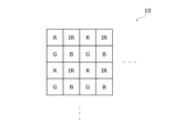
- FIG. 1 is a diagram schematically showing an example of a pixel array of a solid-state imaging device according to an embodiment.
- 1 is a flowchart illustrating an example of processing of a solid-state imaging device according to an embodiment.
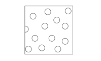
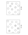
- FIG. 3 is a diagram showing an example of an area to be photographed according to an embodiment. The figure which shows an example of the 1st image and the 2nd image concerning one embodiment.
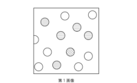
- FIG. 3 is a diagram illustrating an example of an image according to an embodiment.
- FIG. 1 is a diagram schematically showing an example of a solid-state imaging system according to an embodiment.
- FIG. 1 is a diagram schematically showing an example of a solid-state imaging device according to an embodiment.
- the solid-state imaging device 10 includes a pixel array 100, a control circuit 102, a horizontal drive circuit 104, a vertical drive circuit 106, a signal processing circuit 108, and a processing circuit 110.
- the solid-state imaging device 10 is, for example, a device that acquires a first image that is a visible light image and a second image that is an infrared light image of an object in the same range, and processes these images appropriately. .
- the pixel array 100 is an area in which light-receiving pixels having light-receiving elements are arranged in a two-dimensional array. Each light receiving pixel is connected to a pixel circuit.
- the light receiving element outputs a signal according to the intensity of incident light by photoelectric conversion, and the pixel circuit appropriately converts the signal output from the light receiving element into a signal for each pixel and outputs the signal.
- the solid-state imaging device 10 can operate as an area sensor.
- the control circuit 102 is a circuit that controls signal acquisition of the solid-state imaging device 10.
- the control circuit 102 controls the output of signals obtained by photoelectric conversion within the pixel array 100 by the horizontal drive circuit 104 and the vertical drive circuit 106 to the signal processing circuit 108 .
- the control circuit 102 may also be connected to the signal processing circuit 108.
- the horizontal drive circuit 104 selects a line of the pixel array 100 according to the control from the control circuit 102 and drives the light-receiving pixels belonging to the line to output a signal.
- the vertical drive circuit 106 drives the light-receiving pixels belonging to the column at an appropriate timing from the light-receiving pixels belonging to the line selected by the horizontal drive circuit 104 according to the control from the control circuit 102, and outputs a signal. do.
- the signal processing circuit 108 appropriately processes the analog signals output by each light-receiving pixel and outputs them.
- the signal processing circuit 108 may include a column ADC (Analog to Digital Converter) that performs AD (Analog to Digital) conversion for each column, and may convert the analog signal output from the light receiving pixel into a digital signal and output the digital signal.
- the signal processing circuit 108 converts the digital signal into, for example, an image signal using other appropriate circuits and outputs the converted signal.
- the processing circuit 110 performs appropriate processing on the image data output from the signal processing circuit 108.
- the processing circuit 110 may, for example, perform image processing on the image data, or perform information processing such as classification using a rule-based method or classification using a learned model.
- the solid-state imaging device 10 may include a memory circuit.
- the storage circuit can appropriately store image data in the signal processing circuit 108 or the processing circuit 110, for example.
- the processing of the signal processing circuit 108 or the processing circuit 110 is specifically realized by software using information processing using hardware resources, programs necessary for information processing by this software, Executable files and the like may also be stored.
- at least part of the processing of the signal processing circuit 108 or the processing circuit 110 may be realized by each circuit referring to a program stored in a storage circuit.
- the processing circuit 110 is provided inside the solid-state imaging device 10, but the present invention is not limited thereto.
- this processing circuit 110 may be provided outside the solid-state imaging device 10 .
- a pixel array 100, a control circuit 102, a horizontal drive circuit 104, a vertical drive circuit 106, a signal processing circuit 108, and a processing circuit 110 may be formed on the same semiconductor chip, or at least a portion thereof may be formed on the same semiconductor chip.
- the structure may be formed on another semiconductor chip.
- these structures When formed on the same semiconductor chip, these structures may be formed in stacked semiconductor layers, and the layers may be electrically connected by any method such as micro bumps or via holes.
- semiconductor chips When formed by stacking, semiconductor chips are formed by forming individual layers and then stacking them using any method such as CoC (Chip on Chip), CoW (Chip on Wafer), or WoW (Wafer on Wafer). Alternatively, the necessary configurations may be sequentially formed on one substrate.
- FIG. 2 is a diagram showing a non-limiting example of the arrangement of pixels in the pixel array 100 according to one embodiment.
- R means red
- G means green
- B means blue
- IR means equipped with an element that receives infrared light.
- This FIG. 2 may be an array of pixels, or may be an array of divided photoelectric conversion regions (divided pixels) within a pixel.
- some of the light-receiving elements in the Bayer array may be light-receiving elements that can receive infrared light.
- the original array does not have to be a Bayer array, and may include a light-receiving element that receives light other than the three primary colors of RGB.
- the light-receiving element region indicated by IR may be in a form that can receive at least a short wavelength infrared (SWIR) band.
- SWIR short wavelength infrared
- NIR near infrared
- the light-receiving element that receives light in each color band may be, for example, provided with a color filter on the incident surface side of the light-receiving element, or may be formed of an organic photoelectric conversion element. That is, the designation of the band in which light is received by each light receiving element may be implemented using any method.
- the pixel array 100 includes, as non-limiting examples, pixels that can acquire any polarization state, pixels that can acquire image plane phase difference, pixels that can acquire ToF (Time of Flight) information, pixels that can detect event information, At least some of the pixels may include pixels using a plasmon filter.
- the solid-state imaging device 10 can generate images in the visible light band and infrared light band for information on the same object. That is, the solid-state imaging device 10 can acquire a first image, which is an image in the visible light band, and a second image, which is an image in the infrared light band, of the same object.
- the solid-state imaging device 10 operates as an area sensor that images the same area in the visible light band and infrared light band.
- the coordinates of the first and second images basically do not shift, so the solid-state imaging device 10 acquires visible information and infrared information of the same object at the same coordinates. be able to.
- the solid-state imaging device 10 is not applicable only to dry food. It is possible to perform similar processing on any target. Also, as an example, an image in the SWIR band is acquired as the second image, but it is also possible to change this band according to the purpose.
- the data of the first image and second image acquired by the signal processing circuit 108 are sent to the processing circuit 110, and the processing circuit 110 can perform arbitrary processing on these images.
- FIG. 3 is a flowchart showing the processing of the solid-state imaging device 10 according to one embodiment.
- the solid-state imaging device 10 converts visible light band light and infrared light band light in a region that can be received by the pixel array 100 into signals, and outputs the signals (S100).
- the solid-state imaging device 10 for example, photographs an area of dried food where the food is present after drying, receives the light reflected or transmitted by the dried food at a light receiving element in the pixel array 100 , and captures the light for each pixel. Output.
- the signal processing circuit 108 converts the analog signal output from the pixel circuit into a digital signal, and generates the first image by appropriately processing the received light signal in the visible light band (S102). For example, the signal processing circuit 108 appropriately mixes these outputs based on the signals acquired from the light-receiving elements corresponding to the R, G, and B wavelength ranges in FIG. Get the image.
- the processing circuit 110 executes processing on the first image generated by the signal processing circuit 108 (S104). This process is, for example, a process of inspecting the appearance of dried food. The processing circuit 110 inspects, for example, whether there is any defect in the appearance of the dried food shown in the first image, based on the acquired color information.
- the processing circuit 110 can detect foreign matter attached to the dried food and/or detect deterioration or deterioration of the color of the dried food by referring to the first image. For example, the processing circuit 110 can notify the user or the like to re-inspect a dried food for which foreign matter, deterioration or deterioration of color has been detected. Furthermore, based on the output of the processing circuit 110 , a defective product elimination module or the like external to the solid-state imaging device 10 automatically eliminates or removes dried foods that are detected to have foreign objects, deterioration, or deterioration in the lane of the factory, for example. It is also possible to perform a re-inspection by the user.
- the solid-state imaging device 10 may perform processing for acquiring a second image, which is an image in the SWIR band, and processing for the second image. Instead of executing these in parallel, for example, you can process the second image after finishing the processing of the first image, or process the first image after finishing the processing of the second image. It's okay.
- the signal processing circuit 108 converts the analog signal output from the pixel circuit into a digital signal, and generates a second image by appropriately processing the received light signal in the SWIR band (S106). For example, the signal processing circuit 108 acquires a second image, which is an image in the SWIR band, from these outputs based on the signals acquired from the light receiving elements corresponding to the IR wavelength range in FIG. 2.
- the processing circuit 110 executes processing on the second image generated by the signal processing circuit 108 (S108).
- This process is, for example, a process of inspecting the moisture content of dried food.
- Light in the SWIR band has the characteristic of being absorbed by moisture (water). Therefore, the processing circuit 110 can detect the moisture content of the dried food, for example, by referring to the second image.
- the processing circuit 110 compares the moisture content of the dried food with a predetermined threshold by referring to the second image, and if the moisture content is higher than the predetermined threshold, the processing circuit 110 compares the moisture content of the dried food with a predetermined threshold.
- the user may be notified to re-dry the dried food, or an external re-drying process execution module or the like may automatically initiate the re-drying process for dried foods that need to be re-dried, e.g. from a factory lane. may be processed so that it is executed.
- the number of predetermined thresholds does not need to be one, and multiple thresholds may be provided.
- the water content may be acquired as a continuous value.
- the processing circuit 110 may determine the presence or absence of a re-drying process from the moisture content of the dried food, and may also calculate and output the drying time in the re-drying process of the dried food. When determining the moisture content using a threshold value as shown in the example above, the processing circuit 110 may set a drying time within the determined range or obtain it as a continuous value. If necessary, the drying time may be calculated for this continuous value.
- the processing circuit 110 may detect a component that absorbs light in the SWIR band from the acquired second image.
- the processing circuit 110 can, for example, obtain the protein content of the dried food from the second image.
- the processing circuit 110 can also infer the moisture content of the dried food from this protein content.
- the first image in the visible light band and the second image in the SWIR band are displayed at the same timing (or when they are stationary) for objects that exist in the same area. (The timing may be different depending on the object in question.) Therefore, it is possible to perform appropriate processing using the respective information in the visible light band and the SWIR band using the same coordinates without having to perform processing related to the solid-state imaging device 10 such as optical axis alignment.
- the solid-state imaging device 10 can detect defects suitable for visible light in visible light images, as well as detect moisture content of dry objects in SWIR images. information can be obtained.
- solid-state imaging devices 10 can also nondestructively inspect the interior of objects made of resin that transmits light in the SWIR band at the same time as the exterior. be.
- the band of infrared light to be received is not limited to SWIR, and a light receiving element that receives light in the NIR band may also be provided. Further, in the SWIR band, a light receiving element that receives light in a plurality of wavelength regions may be provided. In such a case, it is also possible to detect defects and the like related to different characteristics from images having different characteristics in the infrared light band. For example, in the NIR band, it is possible to detect foreign substances that cannot be detected by visual inspection in areas containing moisture, and in the SWIR band, it is also possible to detect moisture content.
- the processing circuit 110 can also obtain the moisture content of each type of dry food from the second image. For example, the processing circuit 110 receives in advance data regarding the type of food to be photographed by the solid-state imaging device 10, and calculates the moisture content and color density from a data sheet based on the type of food. Data indicating the relationship may be extracted, and based on this data, the moisture content may be detected from the second image.
- the processing circuit 110 can perform the determination process on the first image using the trained model.
- This trained model is trained by machine learning using, for example, images (visible light images) of the target food labeled as good and defective products visually judged by humans (visible light images). It's a model. This label may have multiple labels such as not only good/defective but also no defect, foreign matter attached, and color defect.
- This model may be trained by any machine learning method. This model may determine whether each image is defective (classification), or may determine whether a part of the image (target food) is defective.
- the solid-state imaging device 10 of the present disclosure it is also possible to photograph a plurality of objects and perform various inspections on the plurality of photographed images at the same timing. In this case, by referring to the coordinates or address of the object determined to have a defect, it is possible to obtain information about which object has the defect in the first and second images. .
- FIG. 4 is a diagram showing an example of an area to be photographed.
- the circle in the figure indicates the target object.
- the solid-state imaging device 10 acquires a first image and a second image for an image including such multiple objects.
- FIG. 5 is a diagram showing an example of the first image and the second image in contrast to FIG. 4 above.
- the figure on the left shows an example of the first image, and the figure on the right shows an example of the second image.
- the processing circuit 110 detects that an object indicated by diagonal lines in the first image has an appearance defect, and detects moisture in an object indicated by horizontal lines in the second image.
- the solid-state imaging device 10 it is possible to detect a defective object for each object in each of the first image and the second image.
- FIG. 6 is a diagram showing an image in which the object determined to be defective in the second image is reflected in the first image.
- the processing circuit 110 can also aggregate (synthesize) defective objects determined in each image into one image as shown in FIG. For example, the processing circuit 110 marks objects determined to be defective in the second image in the first image, thereby indicating objects with defective appearance and objects containing moisture on the same image. You can also do that.
- the processing circuit 110 marks an image determined to be defective in both the first image and the second image differently from the object determined to be defective in each image. Since the same optical system is used to acquire information using the pixels included in the same pixel array 100, the solid-state imaging device 10 can easily achieve such image synthesis. For example, when displaying on a display device, markings can be indicated by changing the color of the object, blinking the object, encircling the object, etc., or marking the object as ⁇ defect in appearance'' as text information. It is also possible to display "moisture content: high" or the like.
- the model may be in any form as long as it can make appropriate decisions; as a non-limiting example, it may be in the form of an MLP (Multi-Layer Perceptron) or a form that includes a convolution layer at least in part.
- MLP Multi-Layer Perceptron
- the processing circuit 110 may make a determination based on a rule base, or the second image may be determined by separately learned training in the same manner as above. You may also use a completed model. That is, the processing circuit 110 determines or infers the moisture content (including whether it is contained) and/or the protein content (including whether it is contained) for the second image using the trained model. Good too.
- the trained model inputs either the first image or the second image, but is not limited to this.
- the trained model inputs the data of the first image and the second image from the input layer, and uses the information of both input images to perform inspections of objects such as dried foods (both visual inspection and moisture content inspection). (inspection)).
- the signal processing circuit 108 outputs digital data for each color (including IR band) output from each pixel circuit, and the processing circuit 110 learns the data for each color output from the signal processing circuit 108. It can also be in a form that can be input into a completed model.
- the solid-state imaging device 10 can properly acquire the first image by photographing the object in a state in which a human can sense the object, for example, in a state in which the object is illuminated with light such as sunlight or fluorescent light. can. On the other hand, it is unclear whether the target is irradiated with light in a desired infrared light band. Therefore, the solid-state imaging device 10 may form a solid-state imaging system together with a light source that emits light in at least an infrared light band.
- FIG. 7 is a diagram schematically showing a solid-state imaging system according to an embodiment.
- the solid-state imaging system 1 includes at least a solid-state imaging device 10 and an infrared light source 20.
- the solid-state imaging system 1 may further include a visible light source 22.
- the infrared light source 20 is, for example, a light source that irradiates a target with infrared light.
- This infrared light source 20 is, for example, a light source that emits light including a wavelength in the SWIR band that can generate an image in the solid-state imaging device 10 .
- a light source that includes wavelengths in the NIR band may be used, or information on wavelengths in the NIR band may be acquired separately.
- a corresponding light source may be provided.
- the light source may include light of wavelengths in all of these bands.
- the solid-state imaging system 1 uses an infrared light source 20 to irradiate infrared light onto the food to be inspected, so that the solid-state imaging device 10 can receive light in a desired wavelength band and generate an image. It becomes possible.
- the solid-state imaging system 1 may further include a visible light source 22.
- the visible light source 22 is a light source that includes wavelengths in a band that allows the solid-state imaging device 10 to obtain an appropriate first image.
- the solid-state imaging system 1 shown in FIG. 7 it is possible to generate images based on light in a desired wavelength band in the solid-state imaging device 10. As a result, according to the solid-state imaging system 1 , it is possible to accurately implement the inspection in the solid-state imaging device 10 described above.
- an image sensor having a visible light receiving element that receives visible light and an infrared light receiving element that receives at least infrared light in a short wavelength infrared band in a single pixel array;
- a first image showing an image of the dried food in a visible region and a second image showing an image of the dried food in an infrared region are generated from the data acquired by the image sensor, and the generated second image is a processing circuit that inspects the dried food from the first image and the second image;
- a solid-state imaging device comprising:
- the processing circuit detects the moisture content of the dried food from at least the second image.
- the solid-state imaging device according to (1).
- the processing circuit compares the moisture content with a predetermined threshold and notifies that the dried food product whose moisture content is higher than the predetermined threshold is to be subjected to a re-drying process.
- the solid-state imaging device according to (2) The solid-state imaging device according to (2).
- the processing circuit calculates the drying time of the re-drying step based on the moisture content.
- the processing circuit infers the moisture content of the dried food using a trained model.
- the solid-state imaging device according to any one of (2) to (4).
- the processing circuit detects the protein content of the dried food from at least the second image;
- the solid-state imaging device according to any one of (1) to (5).
- the processing circuit infers the protein content of the dried food using a trained model.
- the processing circuit detects defects in the appearance of the dried food from at least the first image.
- the solid-state imaging device according to any one of (1) to (7).
- the processing circuit detects foreign matter attached to the dried food from the first image.
- the solid-state imaging device according to (8).
- the processing circuit detects deterioration in color of the dried food from the first image;
- the processing circuit performs a visual inspection of the dried food using the learned model.
- the solid-state imaging device according to any one of (8) to (10).
- the processing circuit inspects the dried food based on the first image and the second image using the trained model;
- the solid-state imaging device according to any one of (1) to (11).
- an infrared light source that emits infrared light including at least a short wavelength infrared band
- the solid-state imaging device according to any one of (1) to (12), Equipped with The image sensor receives, with the infrared light receiving element, light emitted from the infrared light source and reflected or transmitted by the dried food. Solid-state imaging system.
- Solid-state imaging system 10: Solid-state imaging device, 100: pixel array, 102: Control circuit, 104: Horizontal drive circuit, 106: Vertical drive circuit, 108: Signal processing circuit, 110: Processing circuit, 20: Infrared light source, 22: Visible light source
Landscapes
- Life Sciences & Earth Sciences (AREA)
- Physics & Mathematics (AREA)
- Health & Medical Sciences (AREA)
- Chemical & Material Sciences (AREA)
- Pathology (AREA)
- Analytical Chemistry (AREA)
- Biochemistry (AREA)
- General Health & Medical Sciences (AREA)
- General Physics & Mathematics (AREA)
- Immunology (AREA)
- Engineering & Computer Science (AREA)
- Spectroscopy & Molecular Physics (AREA)
- Food Science & Technology (AREA)
- Biophysics (AREA)
- Molecular Biology (AREA)
- Computer Vision & Pattern Recognition (AREA)
- Signal Processing (AREA)
- Medicinal Chemistry (AREA)
- Investigating Materials By The Use Of Optical Means Adapted For Particular Applications (AREA)
- Investigating Or Analysing Materials By Optical Means (AREA)
- Solid State Image Pick-Up Elements (AREA)
Abstract
Description
可視光を受光する可視光受光素子と、少なくとも短波長赤外帯域の赤外光を受光する赤外光受光素子と、を単一の画素アレイにおいて有する、撮像素子と、
前記撮像素子が取得したデータから、可視領域における乾燥済み食品の像を示す第 1 画像と、赤外領域における前記前記乾燥済み食品の像を示す第 2 画像と、を生成し、生成した前記第 1 画像及び前記第 2 画像から、前記乾燥済み食品を検査する、処理回路と、
を備える固体撮像装置。
前記処理回路は、少なくとも前記第 2 画像から、前記乾燥済み食品の水分の含有量を検出する、
(1)に記載の固体撮像装置。
前記処理回路は、前記水分の含有量を所定しきい値と比較し、前記水分の含有量が前記所定しきい値よりも高い前記乾燥済み食品を再乾燥工程する対象であることを通知する、
(2)に記載の固体撮像装置。
前記処理回路は、前記水分の含有量に基づいて、前記再乾燥工程の乾燥時間を算出する、
(3)に記載の固体撮像装置。
前記処理回路は、前記乾燥済み食品の水分の含有量を、学習済みモデルを用いて推論する、
(2)から(4)のいずれかに記載の固体撮像装置。
前記処理回路は、少なくとも前記第 2 画像から、前記乾燥済み食品のタンパク質の含有量を検出する、
(1)から(5)のいずれかに記載の固体撮像装置。
前記処理回路は、前記乾燥済み食品のタンパク質の含有量を、学習済みモデルを用いて推論する、
(6)に記載の固体撮像装置。
前記処理回路は、少なくとも前記第 1 画像から、前記乾燥済み食品の外観における不良を検出する、
(1)から(7)のいずれかに記載の固体撮像装置。
前記処理回路は、前記第 1 画像から、前記乾燥済み食品に付着した異物を検出する、
(8)に記載の固体撮像装置。
前記処理回路は、前記第 1 画像から、前記乾燥済み食品の色味の悪化を検出する、
(8)又は(9)に記載の固体撮像装置。
前記処理回路は、前記乾燥済み食品の外観検査を、学習済みモデルを用いて実行する、
(8)から(10)のいずれかに記載の固体撮像装置。
前記処理回路は、学習済みモデルを用いて、前記第 1 画像及び前記第 2 画像に基づいて、前記乾燥済み食品を検査する、
(1)から(11)のいずれかに記載の固体撮像装置。
少なくとも短波長赤外帯域を含む赤外光を射出する、赤外光源と、
(1)から(12)のいずれかに記載の固体撮像装置と、
を備え、
前記撮像素子は、前記赤外光源から射出され、前記乾燥済み食品において反射又は透過した光を前記赤外光受光素子で受光する、
固体撮像システム。
10: 固体撮像装置、
100: 画素アレイ、
102: 制御回路、
104: 水平駆動回路、
106: 垂直駆動回路、
108: 信号処理回路、
110: 処理回路、
20: 赤外光源、
22: 可視光源
Claims (13)
- 可視光を受光する可視光受光素子と、少なくとも短波長赤外帯域の赤外光を受光する赤外光受光素子と、を単一の画素アレイにおいて有する、撮像素子と、
前記撮像素子が取得したデータから、可視領域における乾燥済み食品の像を示す第 1 画像と、赤外領域における前記乾燥済み食品の像を示す第 2 画像と、を生成し、生成した前記第 1 画像及び前記第 2 画像から、前記乾燥済み食品を検査する、処理回路と、
を備える固体撮像装置。 - 前記処理回路は、少なくとも前記第 2 画像から、前記乾燥済み食品の水分の含有量を検出する、
請求項1に記載の固体撮像装置。 - 前記処理回路は、前記水分の含有量を所定しきい値と比較し、前記水分の含有量が前記所定しきい値よりも高い前記乾燥済み食品を再乾燥工程する対象であることを通知する、
請求項2に記載の固体撮像装置。 - 前記処理回路は、前記水分の含有量に基づいて、前記再乾燥工程の乾燥時間を算出する、
請求項3に記載の固体撮像装置。 - 前記処理回路は、前記乾燥済み食品の水分の含有量を、学習済みモデルを用いて推論する、
請求項2に記載の固体撮像装置。 - 前記処理回路は、少なくとも前記第 2 画像から、前記乾燥済み食品のタンパク質の含有量を検出する、
請求項1に記載の固体撮像装置。 - 前記処理回路は、前記乾燥済み食品のタンパク質の含有量を、学習済みモデルを用いて推論する、
請求項6に記載の固体撮像装置。 - 前記処理回路は、少なくとも前記第 1 画像から、前記乾燥済み食品の外観における不良を検出する、
請求項1に記載の固体撮像装置。 - 前記処理回路は、前記第 1 画像から、前記乾燥済み食品に付着した異物を検出する、
請求項8に記載の固体撮像装置。 - 前記処理回路は、前記第 1 画像から、前記乾燥済み食品の色味の悪化を検出する、
請求項8に記載の固体撮像装置。 - 前記処理回路は、前記乾燥済み食品の外観検査を、学習済みモデルを用いて実行する、
請求項8に記載の固体撮像装置。 - 前記処理回路は、学習済みモデルを用いて、前記第 1 画像及び前記第 2 画像に基づいて、前記乾燥済み食品を検査する、
請求項1に記載の固体撮像装置。 - 少なくとも短波長赤外帯域の光を含む赤外光を射出する、赤外光源と、
請求項1に記載の固体撮像装置と、
を備え、
前記撮像素子は、前記赤外光源から射出され、前記乾燥済み食品において反射又は透過した光を前記赤外光受光素子で受光する、
固体撮像システム。
Priority Applications (1)
| Application Number | Priority Date | Filing Date | Title |
|---|---|---|---|
| US18/995,041 US20260016403A1 (en) | 2022-08-09 | 2023-06-20 | Solid-state imaging device and solid-state imaging system |
Applications Claiming Priority (2)
| Application Number | Priority Date | Filing Date | Title |
|---|---|---|---|
| JP2022-127350 | 2022-08-09 | ||
| JP2022127350A JP2024024495A (ja) | 2022-08-09 | 2022-08-09 | 固体撮像装置及び固体撮像システム |
Publications (1)
| Publication Number | Publication Date |
|---|---|
| WO2024034261A1 true WO2024034261A1 (ja) | 2024-02-15 |
Family
ID=89851534
Family Applications (1)
| Application Number | Title | Priority Date | Filing Date |
|---|---|---|---|
| PCT/JP2023/022696 Ceased WO2024034261A1 (ja) | 2022-08-09 | 2023-06-20 | 固体撮像装置及び固体撮像システム |
Country Status (3)
| Country | Link |
|---|---|
| US (1) | US20260016403A1 (ja) |
| JP (1) | JP2024024495A (ja) |
| WO (1) | WO2024034261A1 (ja) |
Families Citing this family (1)
| Publication number | Priority date | Publication date | Assignee | Title |
|---|---|---|---|---|
| WO2026018378A1 (ja) * | 2024-07-18 | 2026-01-22 | ソニーセミコンダクタソリューションズ株式会社 | 光検出装置および測距装置 |
Citations (6)
| Publication number | Priority date | Publication date | Assignee | Title |
|---|---|---|---|---|
| WO2018034166A1 (ja) * | 2016-08-17 | 2018-02-22 | ソニー株式会社 | 信号処理装置および信号処理方法、並びにプログラム |
| JP2018146550A (ja) * | 2017-03-09 | 2018-09-20 | パナソニックIpマネジメント株式会社 | 情報提示システム、及び、情報提示システムの制御方法 |
| JP2020051982A (ja) * | 2018-09-28 | 2020-04-02 | Jfeテクノリサーチ株式会社 | 画像検査装置及び検査モデル構築システム |
| US20200175670A1 (en) * | 2018-11-30 | 2020-06-04 | Boise Cascade Company | Method and system for moisture grading wood products using superimposed near infrared and visual images |
| JP2021022758A (ja) * | 2019-07-24 | 2021-02-18 | ソニー株式会社 | 画像処理装置、撮像装置、および画像処理方法、並びにプログラム |
| JP2021183935A (ja) * | 2020-05-22 | 2021-12-02 | 株式会社Ihi | 節類分類装置、節類分類方法、及び、節類分類プログラム |
-
2022
- 2022-08-09 JP JP2022127350A patent/JP2024024495A/ja active Pending
-
2023
- 2023-06-20 WO PCT/JP2023/022696 patent/WO2024034261A1/ja not_active Ceased
- 2023-06-20 US US18/995,041 patent/US20260016403A1/en active Pending
Patent Citations (6)
| Publication number | Priority date | Publication date | Assignee | Title |
|---|---|---|---|---|
| WO2018034166A1 (ja) * | 2016-08-17 | 2018-02-22 | ソニー株式会社 | 信号処理装置および信号処理方法、並びにプログラム |
| JP2018146550A (ja) * | 2017-03-09 | 2018-09-20 | パナソニックIpマネジメント株式会社 | 情報提示システム、及び、情報提示システムの制御方法 |
| JP2020051982A (ja) * | 2018-09-28 | 2020-04-02 | Jfeテクノリサーチ株式会社 | 画像検査装置及び検査モデル構築システム |
| US20200175670A1 (en) * | 2018-11-30 | 2020-06-04 | Boise Cascade Company | Method and system for moisture grading wood products using superimposed near infrared and visual images |
| JP2021022758A (ja) * | 2019-07-24 | 2021-02-18 | ソニー株式会社 | 画像処理装置、撮像装置、および画像処理方法、並びにプログラム |
| JP2021183935A (ja) * | 2020-05-22 | 2021-12-02 | 株式会社Ihi | 節類分類装置、節類分類方法、及び、節類分類プログラム |
Also Published As
| Publication number | Publication date |
|---|---|
| US20260016403A1 (en) | 2026-01-15 |
| JP2024024495A (ja) | 2024-02-22 |
Similar Documents
| Publication | Publication Date | Title |
|---|---|---|
| JP6945245B2 (ja) | 外観検査装置 | |
| KR20100015628A (ko) | 목재의 검사 방법, 장치 및 프로그램 | |
| WO2019151393A1 (ja) | 食品検査システム、食品検査プログラム、食品検査方法および食品生産方法 | |
| JP6348289B2 (ja) | 検査装置および検査方法 | |
| JP2020051982A (ja) | 画像検査装置及び検査モデル構築システム | |
| US6556291B2 (en) | Defect inspection method and defect inspection apparatus | |
| JP5124705B1 (ja) | はんだ高さ検出方法およびはんだ高さ検出装置 | |
| KR102240757B1 (ko) | Lctf-기반 다분광 영상 기술을 이용한 가공 채소류 내 포함된 이물질 실시간 검출 시스템 | |
| CN102685544B (zh) | 用于检测图像传感器的装置及检测方法 | |
| JP4173184B2 (ja) | Ptp包装品の外観検査装置 | |
| TWI843820B (zh) | 使用多種波長之光單色成像的顏色檢查方法 | |
| KR101012633B1 (ko) | 듀얼 카메라 비전검사 장치 | |
| JP7544358B2 (ja) | 撮像装置、検査装置及び撮像方法 | |
| JP5085860B2 (ja) | 木材の検査方法及び装置及びプログラム | |
| WO2024034261A1 (ja) | 固体撮像装置及び固体撮像システム | |
| JP2020051981A (ja) | 検査装置 | |
| JP2011226814A (ja) | 表面欠陥検査装置及び表面欠陥検査方法 | |
| CN107230648A (zh) | 一种基底缺陷检测装置及检测方法 | |
| US20170005018A1 (en) | Method and device for inspection of a semiconductor device | |
| JP3614980B2 (ja) | 農産物の外観検査方法及び装置 | |
| JP4190243B2 (ja) | 電子回路用部品の外観検査方法及び外観検査装置並びに電子回路用部品の製造方法。 | |
| JP7821228B2 (ja) | マルチスペクトル2d画像データを取得し、光三角測量からの3d画像データに関連付けるための方法および装置 | |
| KR102394422B1 (ko) | Nir 스펙트럼 영상 기술을 이용한 식품 표면 이물 검사 광학장치 | |
| JP2020193867A (ja) | 画像処理装置、制御方法、制御プログラムおよびコンピュータで読み取り可能な記録媒体 | |
| JP4822468B2 (ja) | 欠陥検査装置、欠陥検査方法、及びパターン基板の製造方法 |
Legal Events
| Date | Code | Title | Description |
|---|---|---|---|
| 121 | Ep: the epo has been informed by wipo that ep was designated in this application |
Ref document number: 23852245 Country of ref document: EP Kind code of ref document: A1 |
|
| WWE | Wipo information: entry into national phase |
Ref document number: 18995041 Country of ref document: US |
|
| NENP | Non-entry into the national phase |
Ref country code: DE |
|
| 122 | Ep: pct application non-entry in european phase |
Ref document number: 23852245 Country of ref document: EP Kind code of ref document: A1 |
|
| WWP | Wipo information: published in national office |
Ref document number: 18995041 Country of ref document: US |