WO2024034168A1 - Magnetic sensor - Google Patents
Magnetic sensor Download PDFInfo
- Publication number
- WO2024034168A1 WO2024034168A1 PCT/JP2023/008061 JP2023008061W WO2024034168A1 WO 2024034168 A1 WO2024034168 A1 WO 2024034168A1 JP 2023008061 W JP2023008061 W JP 2023008061W WO 2024034168 A1 WO2024034168 A1 WO 2024034168A1
- Authority
- WO
- WIPO (PCT)
- Prior art keywords
- magnetic field
- wiring
- magnetically permeable
- magnetic
- magnetoresistive element
- Prior art date
Links
- 230000005291 magnetic effect Effects 0.000 title claims abstract description 340
- 230000035945 sensitivity Effects 0.000 claims abstract description 8
- 239000000758 substrate Substances 0.000 claims description 20
- 238000009792 diffusion process Methods 0.000 claims description 8
- 230000000694 effects Effects 0.000 claims description 5
- 239000003302 ferromagnetic material Substances 0.000 claims description 4
- 230000005294 ferromagnetic effect Effects 0.000 abstract description 2
- 230000006698 induction Effects 0.000 abstract 2
- 239000010410 layer Substances 0.000 description 80
- 230000005415 magnetization Effects 0.000 description 30
- 230000004048 modification Effects 0.000 description 11
- 238000012986 modification Methods 0.000 description 11
- 230000003321 amplification Effects 0.000 description 10
- 238000003199 nucleic acid amplification method Methods 0.000 description 10
- YLZOPXRUQYQQID-UHFFFAOYSA-N 3-(2,4,6,7-tetrahydrotriazolo[4,5-c]pyridin-5-yl)-1-[4-[2-[[3-(trifluoromethoxy)phenyl]methylamino]pyrimidin-5-yl]piperazin-1-yl]propan-1-one Chemical compound N1N=NC=2CN(CCC=21)CCC(=O)N1CCN(CC1)C=1C=NC(=NC=1)NCC1=CC(=CC=C1)OC(F)(F)F YLZOPXRUQYQQID-UHFFFAOYSA-N 0.000 description 7
- DEXFNLNNUZKHNO-UHFFFAOYSA-N 6-[3-[4-[2-(2,3-dihydro-1H-inden-2-ylamino)pyrimidin-5-yl]piperidin-1-yl]-3-oxopropyl]-3H-1,3-benzoxazol-2-one Chemical compound C1C(CC2=CC=CC=C12)NC1=NC=C(C=N1)C1CCN(CC1)C(CCC1=CC2=C(NC(O2)=O)C=C1)=O DEXFNLNNUZKHNO-UHFFFAOYSA-N 0.000 description 7
- 238000001514 detection method Methods 0.000 description 7
- 238000010586 diagram Methods 0.000 description 7
- 239000000463 material Substances 0.000 description 7
- 230000008859 change Effects 0.000 description 4
- 230000007423 decrease Effects 0.000 description 4
- 230000004907 flux Effects 0.000 description 4
- 239000000696 magnetic material Substances 0.000 description 4
- 238000004519 manufacturing process Methods 0.000 description 4
- 229910045601 alloy Inorganic materials 0.000 description 3
- 239000000956 alloy Substances 0.000 description 3
- 238000004088 simulation Methods 0.000 description 3
- 229910018072 Al 2 O 3 Inorganic materials 0.000 description 2
- 229910003321 CoFe Inorganic materials 0.000 description 2
- 229910001030 Iron–nickel alloy Inorganic materials 0.000 description 2
- 239000000470 constituent Substances 0.000 description 2
- 239000010949 copper Substances 0.000 description 2
- 238000005259 measurement Methods 0.000 description 2
- 238000000034 method Methods 0.000 description 2
- 239000000203 mixture Substances 0.000 description 2
- 229910000889 permalloy Inorganic materials 0.000 description 2
- 230000008569 process Effects 0.000 description 2
- 229910001313 Cobalt-iron alloy Inorganic materials 0.000 description 1
- RYGMFSIKBFXOCR-UHFFFAOYSA-N Copper Chemical compound [Cu] RYGMFSIKBFXOCR-UHFFFAOYSA-N 0.000 description 1
- 229910052581 Si3N4 Inorganic materials 0.000 description 1
- VYPSYNLAJGMNEJ-UHFFFAOYSA-N Silicium dioxide Chemical compound O=[Si]=O VYPSYNLAJGMNEJ-UHFFFAOYSA-N 0.000 description 1
- GWEVSGVZZGPLCZ-UHFFFAOYSA-N Titan oxide Chemical compound O=[Ti]=O GWEVSGVZZGPLCZ-UHFFFAOYSA-N 0.000 description 1
- XAGFODPZIPBFFR-UHFFFAOYSA-N aluminium Chemical compound [Al] XAGFODPZIPBFFR-UHFFFAOYSA-N 0.000 description 1
- 229910052782 aluminium Inorganic materials 0.000 description 1
- PNEYBMLMFCGWSK-UHFFFAOYSA-N aluminium oxide Inorganic materials [O-2].[O-2].[O-2].[Al+3].[Al+3] PNEYBMLMFCGWSK-UHFFFAOYSA-N 0.000 description 1
- 230000002238 attenuated effect Effects 0.000 description 1
- 230000004888 barrier function Effects 0.000 description 1
- 239000004020 conductor Substances 0.000 description 1
- 229910052802 copper Inorganic materials 0.000 description 1
- PMHQVHHXPFUNSP-UHFFFAOYSA-M copper(1+);methylsulfanylmethane;bromide Chemical compound Br[Cu].CSC PMHQVHHXPFUNSP-UHFFFAOYSA-M 0.000 description 1
- 230000005611 electricity Effects 0.000 description 1
- 230000005293 ferrimagnetic effect Effects 0.000 description 1
- 230000017525 heat dissipation Effects 0.000 description 1
- 238000003475 lamination Methods 0.000 description 1
- CPLXHLVBOLITMK-UHFFFAOYSA-N magnesium oxide Inorganic materials [Mg]=O CPLXHLVBOLITMK-UHFFFAOYSA-N 0.000 description 1
- 239000007769 metal material Substances 0.000 description 1
- 150000004767 nitrides Chemical class 0.000 description 1
- 238000007747 plating Methods 0.000 description 1
- 238000000926 separation method Methods 0.000 description 1
- HQVNEWCFYHHQES-UHFFFAOYSA-N silicon nitride Chemical compound N12[Si]34N5[Si]62N3[Si]51N64 HQVNEWCFYHHQES-UHFFFAOYSA-N 0.000 description 1
- 239000002356 single layer Substances 0.000 description 1
- OGIDPMRJRNCKJF-UHFFFAOYSA-N titanium oxide Inorganic materials [Ti]=O OGIDPMRJRNCKJF-UHFFFAOYSA-N 0.000 description 1
Images


Classifications
-
- G—PHYSICS
- G01—MEASURING; TESTING
- G01R—MEASURING ELECTRIC VARIABLES; MEASURING MAGNETIC VARIABLES
- G01R33/00—Arrangements or instruments for measuring magnetic variables
- G01R33/02—Measuring direction or magnitude of magnetic fields or magnetic flux
-
- G—PHYSICS
- G01—MEASURING; TESTING
- G01R—MEASURING ELECTRIC VARIABLES; MEASURING MAGNETIC VARIABLES
- G01R33/00—Arrangements or instruments for measuring magnetic variables
- G01R33/02—Measuring direction or magnitude of magnetic fields or magnetic flux
- G01R33/06—Measuring direction or magnitude of magnetic fields or magnetic flux using galvano-magnetic devices
- G01R33/09—Magnetoresistive devices
-
- H—ELECTRICITY
- H10—SEMICONDUCTOR DEVICES; ELECTRIC SOLID-STATE DEVICES NOT OTHERWISE PROVIDED FOR
- H10N—ELECTRIC SOLID-STATE DEVICES NOT OTHERWISE PROVIDED FOR
- H10N50/00—Galvanomagnetic devices
- H10N50/10—Magnetoresistive devices
Definitions
- the present invention relates to a magnetic sensor.
- Patent Document 1 has a substrate and a laminated portion disposed on the substrate, and the laminated portion includes a magnetization free layer whose magnetization changes according to an external magnetic field, and a magnetization free layer whose magnetization is fixed in a first direction.
- a magnetically sensitive unit including a magnetization fixed layer and a nonmagnetic layer disposed between the magnetization free layer and the magnetization fixed layer, and outputting a signal according to the external magnetic field; and a magnetization sensitive unit configured to bias the magnetization free layer.
- a magnetic field generating section that applies a magnetic field, and when the bias magnetic field is not applied to the magnetization free layer, the magnetization direction of the magnetization free layer is substantially parallel or substantially opposite to the first direction.
- a magnetic sensor is disclosed that is configured to calculate a component of the external magnetic field in the second direction based on an output.
- a specific example of the magnetic field generating section is a wiring section provided in the lamination direction of the laminated section, and the induced magnetic field from the energized wiring section is applied as a bias magnetic field to the magnetization free layer of the laminated section. is applied to. External magnetic fields are measured while receiving bias magnetic fields applied in different directions, and 1/f noise is removed based on these measurement results.
- the joules from the wiring have a small cross-sectional area. It is sometimes difficult to increase the strength of the induced magnetic field by increasing the amount of current flowing through the wiring, for example because heat is difficult to dissipate due to the structure.
- an object of the present invention is to provide a magnetic sensor that can efficiently apply an induced magnetic field of wiring arranged in the vicinity of a magnetoresistive element.
- a magnetic sensor for solving the above problems includes a pinned magnetic layer, a free magnetic layer, and an intermediate layer formed between the pinned magnetic layer and the free magnetic layer, a magnetoresistive element having a sensitivity axis in a first direction; and a wiring located in a second direction that intersects the first direction along the stacking direction of the magnetoresistive element and having a first surface facing the magnetoresistive element.
- a magnetically permeable part made of a ferromagnetic material provided on at least a part of the surface of the wiring other than the first surface, and the wiring is configured such that an induced magnetic field generated when electricity is applied to the magnetoresistive element in a first direction. It is characterized in that it is arranged so that it is applied in the direction.
- the magnetically permeable portion functions as a magnetic collector that collects the induced magnetic field from the wiring, and can increase the intensity of the induced magnetic field applied to the magnetoresistive element.
- an insulating layer is provided between the wiring and the magnetically permeable part. If the resistivity of the magnetically permeable part is low, the amount of current flowing through the magnetically permeable part will increase if no insulating layer is provided, and as a result, the amount of current flowing through the wiring will be relatively reduced, and the strength of the induced magnetic field will decrease. will decrease.
- the insulating layer is a diffusion suppressing layer that suppresses interdiffusion between the elements constituting the wiring and the elements constituting the magnetically permeable portion.
- the insulating layer suppresses mutual diffusion between the wiring and the magnetically permeable part, the composition of the wiring and/or the magnetically permeable part is less likely to change over time, which improves the quality stability (functional stability) of the sensor. becomes higher.
- a magnetic gap may be provided in the magnetically permeable portion.
- the magnetically permeable part may have the function of a magnetic shield that prevents an external magnetic field from being applied to the magnetoresistive element, but even in such cases, providing a magnetic gap can prevent the magnetically permeable part from being applied. Since the magnetic resistance increases, an external magnetic field is more likely to be applied to the magnetoresistive element.
- the magnetic gap is provided on a second surface of the wiring that faces the first surface along a direction perpendicular to the first direction. Even if the external magnetic field is concentrated in the permeable part, the magnetic resistance on the second surface side is higher, so the external magnetic field can be efficiently guided to the first surface side (the side where the magnetoresistive element is located). .
- a magnetically permeable portion may be provided on at least one of the side surfaces of the wiring that face the first direction.
- the magnetically permeable portion provided on the side surface not only functions as a magnetic collector that collects the induced magnetic field from the wiring, but also functions as a magnetic collector that collects the external magnetic field in the first direction.
- the external magnetic field in the first direction is efficiently concentrated on the magnetically permeable part, so that the magnetic resistance is greater than when no magnetically permeable part is provided.
- a strong external magnetic field can be applied to the effect element.
- a magnetically permeable part is provided on at least a part of the above-mentioned side surface, when the magnetically permeable part does not extend over the second surface, the region on the second surface functions as a magnetic gap, resulting in a magnetoresistive effect.
- An external magnetic field can be efficiently guided to the first surface side where the element is arranged.
- the end portion facing the magnetoresistive element among the end portions on the second direction side of the magnetically permeable portion is It may have a function of converting components in two directions into a first direction and applying it to the magnetoresistive element.
- the magnetic sensor has a function of detecting an external magnetic field in the second direction.
- the wiring and the magnetoresistive element may be formed on the same substrate.
- the wiring and the magnetoresistive element are formed on the same substrate, the wiring also has the same size as the magnetoresistive element, so it is not easy to increase the amount of current flowing through the wiring. Even in such a case, if the sensor has a configuration that strengthens the induced magnetic field from the wiring like the magnetic sensor described above, it is possible to effectively achieve the purpose of noise removal.
- the first direction is one of the in-plane directions of the substrate and the second direction is the thickness direction of the substrate.
- a magnetic sensor that can efficiently apply an induced magnetic field of wiring arranged near a magnetoresistive element.
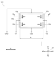
- FIG. 1 is a circuit diagram of a magnetic sensor according to an embodiment of the present invention.
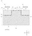
- 2 is a sectional view taken along line A-A' in FIG. 1.
- FIG. 3 is a graph showing the relationship between the efficiency of the bias magnetic field and the width of the permeable portion as a result of Example 1.
- FIG. 3 is a graph showing the relationship between the amplification factor of the external magnetic field and the width of the permeable portion as a result of Example 1.
- FIG. FIG. 3 is a cross-sectional view illustrating the structure of a magnetic sensor according to Example 2-1.
- FIG. 3 is a cross-sectional view illustrating the structure of a magnetic sensor according to Example 2-2.
- FIG. 7 is a cross-sectional view illustrating the structure of a magnetic sensor according to Example 2-3.
- FIG. 7 is a cross-sectional view illustrating the structure of a magnetic sensor according to Example 2-6.
- FIG. 7 is a cross-sectional view illustrating a modification of the magnetic sensor according to Example 2-6.
- FIG. 7 is a circuit diagram of a magnetic sensor according to Example 2-7. 10 is a sectional view taken along line B-B' in FIG. 9.
- FIG. 7 is a cross-sectional view illustrating a modification of the magnetic sensor according to Example 2-7. It is a sectional view explaining the structure of the magnetic sensor concerning an example of the modification of one embodiment of the present invention. It is a sectional view explaining the structure of the magnetic sensor concerning another example of the modification of one embodiment of the present invention.
- FIG. 7 is a cross-sectional view illustrating the structure of a magnetic sensor according to another example of a modification of the embodiment of the present invention.
- FIG. 1 is a circuit diagram of a magnetic sensor according to an embodiment of the present invention.
- FIG. 2 is a cross-sectional view taken along line A-A' in FIG.
- a magnetic sensor 100 according to an embodiment of the present invention includes magnetoresistive elements 10a, 10b, 10c, and 10d (referred to as magnetoresistive elements 10, if not distinguished). ing.
- the four magnetoresistive elements 10 may be provided on the same substrate (one chip). In this embodiment, the four magnetoresistive elements 10 are provided on the same substrate (not shown), and FIG. This is a diagram seen from. That is, in FIG.
- the Z1 side in the Z1-Z2 direction is the front side of the substrate, and the Z2 side in the Z1-Z2 direction is the back side of the substrate. Note that the Z1-Z2 direction is along the stacking direction of the magnetoresistive element 10.
- the magnetic sensor 100 has a magnetoresistive element 10a and a magnetoresistive element 10b connected in series between a power supply terminal Vdd, which is a power supply point, and a ground terminal GND, both of which extend in the Y direction.
- a first half-bridge circuit and a second half-bridge circuit in which a magnetoresistive element 10c and a magnetoresistive element 10d, both of which extend in the Y direction, are connected in series are connected in parallel.
- the first half-bridge circuit includes an output terminal V1 between the magnetoresistive element 10a and the magnetoresistive element 10b.
- the second half-bridge circuit also includes an output terminal V2 between the magnetoresistive element 10c and the magnetoresistive element 10d.
- the magnitude of the external magnetic field applied from the outside as the detection magnetic field H can be quantitatively measured by the potential difference (Va-Vb, midpoint potential difference) between the outputs from these two output terminals V1 and V2.
- the magnetization direction of the pinned magnetic layer 11 is in the X1-X2 direction X2 in this order, as shown by the white arrow in FIG. and X1-X2 direction.
- the magnetization direction of the pinned magnetic layer 11 is in the X1-X2 direction X1 in this order, as indicated by the white arrow in FIG. direction and the X1-X2 direction.
- the magnetization directions of the pinned magnetic layers 11 of the magnetoresistive elements 10a and 10c on the power terminal Vdd side are opposite (antiparallel). Furthermore, the magnetization directions of the pinned magnetic layers 11 of the magnetoresistive elements 10b and 10d on the ground terminal GND side are opposite (antiparallel). Therefore, the sensitivity axis direction of the magnetoresistive element 10 is the X1-X2 direction, which is also referred to as the "first direction" in this specification.
- the four magnetoresistive elements 10a to 10d have the same magnetization direction of the free magnetic layer 12 (direction of the bias magnetic field) in a state where no external magnetic field is applied, as shown by black arrows in FIG. It is along the Y1-Y2 direction Y2 direction so that the
- the magnetic sensor 100 can detect the detection magnetic field H with high accuracy.
- a first or second half-bridge circuit or a magnetoresistive element 10 may be used instead of the full-bridge circuit.
- the magnetoresistive element 10a for example, a GMR element (giant magnetoresistive element) or a TMR element (tunnel magnetoresistive element) is used, and a fixed magnetic layer 11 and a free magnetic layer are used. 12, and an intermediate layer 13 formed between the pinned magnetic layer 11 and the free magnetic layer 12.
- the resistance value of the magnetoresistive element 10a changes depending on the relative relationship between the magnetization directions of the fixed magnetic layer 11 whose magnetization direction is fixed and the free magnetic layer 12 whose magnetization direction is changed by an external magnetic field.
- the magnetic sensor 100 can measure the direction and strength of the external magnetic field to be measured based on the change in the resistance value of the magnetoresistive element 10a.
- the pinned magnetic layer 11 is configured using a ferromagnetic layer such as a CoFe alloy (cobalt-iron alloy), for example.
- the free magnetic layer 12 is made of a soft magnetic material such as a CoFe alloy or a NiFe alloy (nickel-iron alloy), and is formed as a single layer structure, a laminated structure, a laminated ferrimagnetic structure, or the like.
- the intermediate layer 13 is, for example, a non-magnetic intermediate layer made of a non-magnetic material such as Cu.
- a bias magnetic field is applied to the free magnetic layer 12 in a direction perpendicular to the sensitivity axis direction (first direction) in order to stabilize the output of the magnetic sensor 100.
- the direction of the bias magnetic field is the Y1-Y2 direction Y2.
- the fixed magnetic layer 11 of the magnetoresistive element 10a has its magnetization direction fixed in the X1-X2 direction
- the free magnetic layer 12 has its magnetization direction fixed in the X1-X2 direction when no magnetic field is applied. It is oriented in the Y1-Y2 direction Y2, which is perpendicular to the magnetization direction of the layer 11. Therefore, the resistance value of the magnetoresistive element 10a changes in the opposite direction depending on whether the direction of the detected magnetic field H is the X1 direction or the X2 direction in the X1-X2 direction. That is, since the resistance value becomes an odd function with respect to the detected magnetic field H in the X1-X2 direction, the direction and magnitude of the detected magnetic field H can be continuously measured.
- the magnetoresistive element 10a a TMR element may be used instead of the above-mentioned GMR element.
- the intermediate layer 13 is an insulating barrier layer made of MgO, Al 2 O 3 , titanium oxide, or the like.
- the magnetoresistive elements 10b to 10d have the same basic structure as the magnetoresistive element 10a. From the viewpoint of improving measurement accuracy, these magnetoresistive elements 10a to 10d are preferably manufactured on the same substrate by a common manufacturing process.
- a magnetic field generating section MG1 is provided on the Z2 side of the Z1-Z2 direction of the magnetoresistive elements 10a and 10b, and a magnetic field generating part MG1 is provided on the Z2 side of the Z1-Z2 direction of the magnetoresistive elements 10c and 10d.
- a magnetic field generating section MG2 is provided.
- the magnetic field generating section MG1 and the magnetic field generating section MG2 have the same structure.
- the magnetic field generating unit MG1 is located on the Z2 side of the magnetoresistive element 10a in the Z1-Z2 direction, and has a wiring 20 extending in the Y1-Y2 direction. That is, the wiring 20 is located on the Z1-Z2 direction side, which is a second direction intersecting the first direction (X1-X2 direction), of the magnetoresistive element 10a, and is located opposite to the magnetoresistive element 10a. - It has a first surface 21 facing toward the Z1 side in the Z2 direction.
- the wiring 20 is formed so as to be embedded in a substrate (not shown) together with the magnetoresistive element 10a.
- the material constituting the wiring 20 is not particularly limited as long as it is a conductor, and is preferably a material based on a non-magnetic element such as copper or aluminum. Note that it may be advantageous in manufacturing that the first direction is one of the in-plane directions of the substrate and the second direction is the thickness direction of the substrate.
- the distance between the wiring 20 and the magnetoresistive element 10a is set so that a predetermined induced magnetic field from the wiring 20 is applied to the magnetoresistive element 10a.
- the separation distance is set to, for example, a micron order or a submicron order.
- an induced magnetic field along the sensitivity axis direction (first direction, X1-X2 direction) is applied as a bias magnetic field to the free magnetic layer 12 of the magnetoresistive element 10a.
- the width (length in the X1-X2 direction) and height (length in the Z1-Z2 direction) of the wiring 20 are approximately several ⁇ m, and as described above, the wiring 20 is embedded in the substrate. Therefore, there is a limit to the amount of current that can be passed through the wiring 20 due to the heat dissipation efficiency of Joule heat. Therefore, there is a limit to increasing the induced magnetic field applied to the free magnetic layer 12 by increasing the amount of current flowing through the wiring 20.
- the problem that the amount of current flowing through the wiring 20 has a substantial upper limit tends to become apparent.
- the magnetic field generating section MG1 of the magnetic sensor 100 includes a permeable section 30 made of a ferromagnetic material and provided on at least a portion of the surface of the wiring 20 other than the first surface 21.
- the magnetic sensor 100 since the cross-sectional shape of the wiring 20 in the XY plane is rectangular, the surfaces other than the first surface 21 of the wiring 20 face the first surface 21 in the second direction. and two surfaces (third surface 23 and fourth surface 24) facing in the first direction (X1-X2 direction).
- the magnetically permeable part 30 includes a first magnetically permeable part 31 provided on the third surface 23 and a second magnetically permeable part 32 provided on the fourth surface 24 among these surfaces.
- the magnetically permeable part 30 collects the induced magnetic field from the wiring 20 and generates a bias magnetic field along the first direction (X1-X2 direction) using the magnetoresistive effect.
- the voltage can be efficiently applied to the free magnetic layer 12 of the element 10a.
- the magnetic field of appropriate intensity is applied to the induced magnetic field of the wiring 20. It can be applied by
- the constituent material of the magnetically permeable part 30 is not particularly limited as long as it is a ferromagnetic material.
- a specific example is a soft magnetic material such as permalloy.
- the distance between the magnetically permeable part 30 and the wiring 20 is not limited.
- the size may be several ⁇ m, which is equivalent to the size (height, width) of the wiring 20.
- the length (first direction length) of the magnetically permeable part 30 (the first magnetically permeable part 31 and the second magnetically permeable part 32) in the first direction (X1-X2 direction) is the bias that should be applied to the free magnetic layer 12. It is set appropriately depending on the strength of the magnetic field. If the length in the first direction is excessively short, the magnetically permeable portion 30 will have difficulty appropriately fulfilling the function of concentrating the induced magnetic field. Furthermore, if the length in the first direction is excessively long, the induced magnetic field is dispersed inside the magnetically permeable part 30, so the strength of the induced magnetic field applied to the free magnetic layer 12 as a bias magnetic field along the first direction. becomes difficult to increase.
- the magnetically permeable portion 30 having a long length in the first direction may effectively function as a magnetic collector for the external magnetic field in the first direction. Therefore, the length in the first direction is preferably set from the viewpoint of the ratio between the intensity of the induced magnetic field applied to the free magnetic layer 12 and the intensity of the external magnetic field.
- the magnetic field generating section MG1 of the magnetic sensor 100 has an insulating layer 40 between the wiring 20 and the magnetically permeable section 30.
- the magnetically permeable part 30 is made of a metallic material such as permalloy, its resistivity is relatively low, so if the insulating layer 40 is not provided, current will also flow through the magnetically permeable part 30 when energized, and as a result, The amount of current flowing through the wiring 20 is relatively reduced, and the intensity of the magnetic field induced from the wiring 20 is reduced.
- the material and thickness of the insulating layer 40 are arbitrary as long as the current flowing through the wiring 20 can be prevented from flowing into the magnetically permeable part 30. It is preferable that the insulating layer 40 is a diffusion suppressing layer that suppresses mutual diffusion between the elements constituting the wiring 20 and the elements constituting the magnetically permeable portion 30. When the insulating layer 40 suppresses mutual diffusion between the wiring 20 and the magnetically permeable portion 30, the compositions of both are unlikely to change over time, and the quality stability (functional stability) of the magnetic sensor 100 increases.
- the constituent materials of the insulating layer 40 include oxide materials such as silica (SiO 2 ) and alumina (Al 2 O 3 ), silicon nitride (Si 3 N 4 ), and aluminum nitride ( A nitride-based material such as AlN) may be used, and the thickness thereof may preferably be 50 nm or more.
- the magnetic sensor according to the example has the same circuit configuration (full bridge circuit) as the magnetic sensor 100 according to the above-described embodiment, and has four magnetoresistive elements 10a to 10d.
- the difference between each embodiment is the structure of the magnetic field generating sections MG1 and MG2. Therefore, in the following Examples (excluding Examples 2-7), the structure thereof will be explained while showing a cross-sectional view similar to the cross-sectional view taken along the line A-A' of the magnetic sensor 100.
- the magnetic sensor 100 according to Example 1 has a cross-sectional structure shown in FIG. 2. That is, the magnetic field generating section MG1 is located on the Z2 side of the magnetoresistive element 10a in the Z1-Z2 direction, and has the wiring 20 extending in the Y1-Y2 direction. Among the surfaces of the wiring 20, a first magnetically permeable portion 31 and a second magnetically permeable portion 32 are provided on a third surface 23 and a fourth surface 24 facing in the first direction (X1-X2 direction), and a magnetoresistive element The magnetically permeable portion 30 is not provided on the first surface 21 facing the first surface 10a and the second surface 22 facing the first surface 21. An insulating layer 40 is provided between the first magnetically permeable part 31 and the second magnetically permeable part 32 and the wiring 20.
- the length of the magnetoresistive element 10a in the X1-X2 direction is 1.0 ⁇ m, and the length in the Y1-Y2 direction (element length) is 64 ⁇ m.
- the length of the wiring 20 in the X1-X2 direction (wiring width Wp) is 2.0 ⁇ m, the length in the Z1-Z2 direction (wiring height Hp) is 1.5 ⁇ m, and the length in the Y1-Y2 direction (wiring width Wp) is 2.0 ⁇ m. length) is 80 ⁇ m.
- the distance between the magnetoresistive element 10a and the wiring 20 is 0.25 ⁇ m, and the thickness of the insulating layer 40 is 0.5 ⁇ m.
- the length of the first magnetically permeable portion 31 and the second magnetically permeable portion 32 in the Y1-Y2 direction is 80 ⁇ m, which is equal to the wiring length, and the length of the first magnetically permeable portion 31 in the X1-X2 direction.
- the length (first magnetically permeable portion width Wm1) and the length of the second magnetically permeable portion 32 in the X1-X2 direction (second magnetically permeable portion width Wm2) are changed to equal lengths in the range of 0.2 ⁇ m to 16 ⁇ m. did.
- the width of these magnetically permeable parts will be abbreviated as "magnetically permeable part width.”
- the current flowing through the wiring 20 is 1 mA, and the strength of the external magnetic field applied in the first direction (X1-X2 direction) is 1 mT.
- the relationship between the efficiency of the bias magnetic field and the width of the magnetically permeable portion has a maximum value when the magnetically permeable portion width is approximately 2 ⁇ m.
- the results obtained were as follows. When the width of the permeable part is up to about 2 ⁇ m, the magnetic field induced from the wiring 20 is efficiently concentrated in the permeable part 30 by providing the permeable part 30, and the collected magnetic field is applied to the magnetoresistive element 10a. Therefore, the efficiency of the bias magnetic field is improved.
- the width of the permeable part is larger than about 2 ⁇ m, the efficiency of the bias magnetic field decreases, and when the width of the permeable part is 15 ⁇ m or more, the case where the permeable part 30 is not provided (Example 2-1 described later) becomes equivalent to This is because if the width of the magnetically permeable part becomes too large, the induced magnetic field will be dispersed inside the magnetically permeable part 30, and the magnetic collecting function of the magnetically permeable part 30 will deteriorate.
- the relationship between the amplification factor of the external magnetic field and the width of the permeable portion was approximately linear. That is, the magnetically permeable part 30 (first magnetically permeable part 31, second magnetically permeable part 32) according to the first embodiment has a function of concentrating an external magnetic field in the first direction and applying it to the magnetoresistive element 10a. It was confirmed that this function becomes stronger as the width of the permeable part increases. Further, in the graph shown in FIG.
- the magnetically permeable portion 30 according to the first embodiment since the amplification factor is 1 when the width of the magnetically permeable portion is 1 ⁇ m, the magnetically permeable portion 30 according to the first embodiment (the first magnetically permeable portion 31, the second magnetically permeable portion In 32), it was also confirmed that the shielding function for shielding the external magnetic field in the first direction from being applied to the magnetoresistive element 10a does not become apparent if the magnetically permeable portion width is 1 ⁇ m or more.
- Example 2 In Example 1, the influence of the permeable part width on the efficiency of the bias magnetic field and the amplification factor of the external magnetic field was evaluated, but in this example, the influence when the shape of the permeable part 30 was further changed was evaluated. . Simulations were performed for a plurality of magnetic field generating sections MG1 in which the magnetically permeable sections 30 have different shapes.
- the magnetic field generating unit MG1 according to Example 2-1 has a first magnetically permeable portion width Wm1 and a second magnetically permeable portion width Wm2 of 0 ⁇ m, and is provided with an insulating layer 40.
- the shape of the wiring 20 is the same as in Example 1 (wiring width Wp: 2.0 ⁇ m, wiring height Hp: 1.5 ⁇ m, wiring length: 64 ⁇ m), and the distance between the magnetoresistive element 10a and the wiring 20 is is also the same as in Example 1 (0.25 ⁇ m).
- the direction in which the external magnetic field is applied is the first direction (X1-X2 direction).
- the magnetic field generating unit MG1 according to Example 2-2 has a thickness of 0 on the second surface 22, third surface 23, and fourth surface 24 of the wiring 20 having the same shape as in Example 1.
- a magnetically permeable portion 30 of .5 ⁇ m is provided. That is, the magnetically permeable part 30 of the magnetic field generating part MG1 according to Example 2-2 includes a first magnetically permeable part 31 having a first magnetically permeable part width Wm1 of 0.5 ⁇ m, and a second magnetically permeable part width Wm2 of 0.5 ⁇ m.
- the direction in which the external magnetic field is applied is the first direction (X1-X2 direction).
- the magnetic field generating section MG1 according to the embodiment 2-3 has a structure similar to that of the embodiment 2-2, and has a thickness of 0.1 ⁇ m between the wiring 20 and the magnetically permeable section 30. It has an insulating layer 40 of.
- the direction in which the external magnetic field is applied is the first direction (X1-X2 direction).
- Example 2-4 The magnetic field generating unit MG1 according to Example 2-4 has the structure shown in FIG.
- the second magnetically permeable portion width Wm2) is 0.5 ⁇ m in both cases.
- the direction in which the external magnetic field is applied is the first direction (X1-X2 direction).
- Example 2-5 The magnetic field generation unit MG1 according to Example 2-5 has the structure shown in FIG.
- the second magnetically permeable portion width Wm2) is 16 ⁇ m in both cases.
- the direction in which the external magnetic field is applied is the first direction (X1-X2 direction).
- the magnetic field generating unit MG1 according to the embodiment 2-6 has a magnetic field generating section MG1 on the third surface 23 and the fourth surface 24 of the wiring 20 having the same shape as in the embodiment 1, in the same way as in the embodiment 2-5.
- a first magnetically permeable part 31 with a first magnetically permeable part width Wm1 of 16 ⁇ m is provided on the third surface 23, and a second magnetically permeable part 32 with a second magnetically permeable part width Wm2 of 16 ⁇ m is provided on the fourth surface 24.
- the first magnetically permeable portion 31 has a first extending portion 331 extending onto the second surface 22 of the wiring 20, and the extending width We1 is 0.6 ⁇ m.
- the second magnetically permeable portion 32 also has a second extending portion 332 extending onto the second surface 22 of the wiring 20, and the extending width We2 is 0.6 ⁇ m.
- the magnetic field generating section MG1 according to Example 2-6 has the third magnetically permeable section 33 having the magnetic gap G with a width (gap width Wg) of 1.0 ⁇ m on the second surface 22 of the wiring 20. .
- the direction in which the external magnetic field is applied is the first direction (X1-X2 direction).
- the magnetic sensor 101 according to the embodiment 2-7 is different from the magnetic sensor 100 according to the other embodiments in that it measures an external magnetic field in the second direction (Z1-Z2 direction).
- its circuit configuration is similar to the magnetic sensor 100 shown in FIG. X1-X2 direction).
- a magnetic field generating section MG is provided on the second direction (Z1-Z2 direction) Z2 side of the four magnetoresistive elements 10a to 10d.
- the arrangement pitch P between the magnetoresistive elements 10a and 10c that are arranged adjacent to each other in the first direction (X1-X2 direction) is 12.2 ⁇ m.
- FIG. 10A is a cross-sectional view taken along line B-B' in FIG. 9.
- a wiring 202 having a first surface 212 facing the magnetoresistive element 10a is provided on the Z2 side of the magnetoresistive element 10a in the second direction (Z1-Z2 direction).
- a wiring 201 having a first surface 211 facing the magnetoresistive element 10c is provided on the Z2 side in the second direction (Z1-Z2 direction) of the effect element 10c.
- Insulating layers 40 are provided on the second surface 221 and fourth surface 241 of the wiring 201 and on the second surface 222 and third surface 232 of the wiring 202, and these insulating layers 40 are a continuous body.
- a magnetically permeable portion 30 is provided between the wiring 201 and the wiring 202 in the first direction (X1-X2 direction) so as to fill this gap, and the width Wm of the magnetically permeable portion is 10 ⁇ m.
- the magnetically permeable portion 30 is also provided on the Z2 side in the second direction (Z1-Z2 direction) of each of the wiring 201 and the wiring 202, and has a length in the second direction (Z1-Z2 direction) from the second surfaces 221 and 222.
- the height (height Hm of the magnetically permeable part) is 10 ⁇ m.
- Example 2 when the magnetically permeable part 30 is provided to cover areas other than the first surface 21 (Example 2-2), and when the magnetically permeable part 30 is not provided (Example 2-1) In contrast, the bias magnetic field increases significantly (2.8 times), but the detection magnetic field H attenuates (0.22 times). The same results as in Example 2-2 were also obtained when the insulating layer 40 was provided between the magnetically permeable portion 30 and the wiring 20 (Example 2-3).
- the magnetically permeable portion 30 is provided so as to cover the second surface 22, the third surface 23, and the fourth surface 24, so that the wiring 20 is It is considered that the induced magnetic field is efficiently concentrated by the permeable portion 30 and applied to the magnetoresistive element 10a.
- the magnetic field generating unit MG1 of these embodiments is provided with the magnetically permeable portion 30 having a U-shaped cross section, the external magnetic field in the first direction (X1-X2 direction) is directed to the side of the magnetically permeable portion 30.
- the collected magnetic flux passes through the third magnetically permeable part 33 to the other side of the magnetically permeable part 30 (the second magnetically permeable part 32).
- the intensity of the detection magnetic field H detected by the magnetoresistive element 10a decreases. That is, in the magnetic field generating section MG1 of Example 2-2 and the magnetic field generating section MG1 of Example 2-3, results were obtained in which the shielding function of the external magnetic field became apparent.
- Example 2-4 When the magnetically permeable part 30 is not provided on the second surface 22 (Example 2-4), the bias magnetic field is attenuated (about 1/2) compared to Example 2-3, but the detection magnetic field H is The degree of attenuation was reduced, and was approximately 90% of that in the case where the permeable portion 30 was not provided (Example 2-1).
- the magnetic field generating part MG1 of Example 2-4 does not have the magnetically permeable part 30 on the second surface 22. That is, the magnetic field generating part MG1 of Example 2-4 is different from the magnetic field generating part MG1 of Example 2-3.
- the third magnetically permeable portion 33 is not provided, the induced magnetic field around the Y1-Y2 direction of the wiring 20 is less likely to be collected by the magnetically permeable portion 30 than in the magnetic field generating portion MG1 of Example 2-3. For this reason, it is considered that the strength of the bias magnetic field was relatively reduced.
- the magnetic field generating section MG1 of Example 2-4 does not have the third magnetically permeable section 33 in contrast to the magnetic field generating section MG1 of Example 2-3, one side of the magnetically permeable section 30 (for example, the third The magnetic flux of the external magnetic field concentrated in the first magnetically permeable part 31) passes through the first surface 21 side and the other when going to the other side of the magnetically permeable part 30 (the second magnetically permeable part 32). There is virtually no difference between the case of passing through the second surface and the 22 side.
- the magnetic flux passing through the first surface 21 side increases, As a result, it is considered that the intensity of the detected magnetic field H in the magnetoresistive element 10a increased.
- the magnetic field generating section MG1 of Example 2-5 has a width of the first magnetically permeable section 31 (first magnetically permeable section width Wm1) and a second magnetically permeable section in comparison with the magnetic field generating section MG1 of Example 2-4. 32 (second magnetically permeable portion width Wm2) is large.
- the amplification factor of the external magnetic field is larger in Example 1, and in Example 2-5, the amplification factor of the external magnetic field is also larger than in Example 2-4 ( Approximately 3.8 times).
- the magnetic field generating part MG1 of Example 2-6 has a magnetically permeable part 30 extending to the second surface 22 side (first extending part 331, second extension portion 332). These extending portions correspond to the third magnetically permeable portion 33 having a magnetic gap G having a width Wg of 1.0 ⁇ m on the second surface 22.
- the efficiency of the bias magnetic field is lower than that when the third magnetic permeable section 33 is not provided with the magnetic gap G (Example 2-3, 0 .45 mT/mA), but in the case where the third permeable portion 33 is not provided on the second surface 22 (Example 2-4 and Example 2-5, 0.22 mT/mA), in other words.
- a higher result (0.27 mT/mA) was obtained than when a magnetic gap G with a width Wg of 2.0 ⁇ m is provided on the second surface 22 side.
- the amplification factor of the external magnetic field is higher than that in the case where the third magnetic permeable part 33 is not provided with the magnetic gap G (Example 2-3, 0.22 mT/mT). 3. The result was lower (2.28 mT/mT) than in the case where the magnetically permeable portion 33 was not provided (Example 2-4 and Example 2-5, 3.39 mT/mT).
- Example 2-7 In the magnetic field generation unit MG of Example 2-7, one of the surfaces facing in the first direction (the fourth surface 241 for the wiring 201 and the third surface 232 for the wiring 202) and the second surface 221 or the second surface 222 Since the magnetically permeable portion 30 was provided in the magnetic field, the induced magnetic fields of the wirings 201 and 202 were appropriately concentrated, and the efficiency of the bias magnetic field was obtained to be equivalent to that in Example 2-6.
- Embodiment 2-7 differs from other embodiments in that it has a structure for detecting an external magnetic field in the second direction (Z1-Z2 direction).
- FIG. 11 is a diagram showing an example of a modification of the magnetic sensor according to the present embodiment. Similar to FIG. 2, FIG. 11 is a cross-sectional view including a cross section of one magnetoresistive element 10a and the corresponding magnetic field generating section MG1. As shown in FIG. 11, in contrast to the magnetic sensor 100 shown in FIG. It has a wiring 20A having the same shape as 20. As current flows in opposite directions through the wiring 20 and the wiring 20A, an induced magnetic field in the same direction is applied to the free magnetic layer 12 of the magnetoresistive element 10a.
- FIG. 11 is a diagram showing an example of a modification of the magnetic sensor according to the present embodiment. Similar to FIG. 2, FIG. 11 is a cross-sectional view including a cross section of one magnetoresistive element 10a and the corresponding magnetic field generating section MG1. As shown in FIG. 11, in contrast to the magnetic sensor 100 shown in FIG. It has a wiring 20A having the same shape as 20. As current flows in opposite directions through the wiring 20 and the wiring 20A
- a current flows in the wiring 20 in the Y1-Y2 direction Y1 side, and a current flows in the wiring 20A in the Y1-Y2 direction Y2 side, so that an induced magnetic field is generated in the free magnetic layer 12 of the magnetoresistive element 10a. is applied in the X1-X2 direction X2 direction. This direction is equal to the magnetization direction of the pinned magnetic layer 11 of the magnetoresistive element 10a.
- FIG. 12 is a diagram showing another example of a modification of the magnetic sensor according to the present embodiment. Similar to FIG. 2, FIG. 12 is a cross-sectional view including a cross section of one magnetoresistive element 10a and the corresponding magnetic field generating section MG1.
- the magnetoresistive element 10a has three magnetoresistive elements 10a1, 10a2, and 10a3, all of which have the pinned magnetic layer 11 in the same direction (X1-X2 direction X2 direction). It is magnetized (white arrow).
- Magnetic field generating sections having the same structure as the magnetic field generating section MG1 of Example 2-4 are provided on both sides of the second direction (Z1-Z2 direction) of each of the magnetoresistive element 10a1, the magnetoresistive element 10a2, and the magnetoresistive element 10a3.
- MG0 is provided. Therefore, in the magnetic sensor 103 according to this example, the magnetic field generating section MG1 has six magnetic field generating sections MG0.
- the wirings 20 of the three magnetic field generating units MG0 provided on the Z1 side are arranged along the first direction (X1-X2 direction) to form parallel coils, and all of them are arranged along the first direction (X1-X2 direction).
- the wiring 20 of the three magnetic field generating units MG0 provided on the Z2 side in the second direction (Z1-Z2 direction) is also arranged along the first direction (X1-X2 direction) to form parallel coils, and all of them are arranged in the Y1- Current flows in the Y1 direction in the Y2 direction.
- the induced magnetic field of the wiring 20 is applied to each of the three magnetoresistive elements 10a1, 10a2, and 10a3 in the direction along the magnetization direction of the pinned magnetic layer 11.
- FIG. 13 is a diagram showing another example of a modification of the magnetic sensor according to the present embodiment. Similar to FIG. 2, FIG. 13 is a cross-sectional view including a cross section of one magnetoresistive element 10a and the corresponding magnetic field generating section MG1.
- the magnetoresistive element 10a similarly to the magnetic sensor 103, the magnetoresistive element 10a has three magnetoresistive elements 10a1, 10a2, and 10a3, all of which are oriented in the same direction (X1-X2 direction ), the pinned magnetic layer 11 is magnetized (white arrow).
- the wiring 201 has a first surface 21 facing the magnetoresistive element 10a1 in the second direction
- the wiring 202 has a first surface 21 facing the magnetoresistive element 10a2 in the second direction
- the wiring 203 has a first surface 21 facing the magnetoresistive element 10a3 in the second direction.
- the magnetically permeable portion 30 of any of the magnetic field generating units MG0 is not provided on the first surface 21 of the wirings 201, 202, and 203, and the magnetic gap G is provided on the second surface 22 side of the wiring 202.
- a current flows in the Y2 side in the Y1-Y2 direction through the wirings 201, 202, 203 of the magnetic field generating unit MG0 provided on the Z1 side in the second direction (Z1-Z2 direction).
- a current flows in the Y1 side in the Y1-Y2 direction through the wirings 201, 202, 203 of the magnetic field generating unit MG0 provided on the Z2 side in the second direction (Z1-Z2 direction).
- the induced magnetic field of the wiring 20 is applied to each of the three magnetoresistive elements 10a1, 10a2, and 10a3 in the direction along the magnetization direction of the pinned magnetic layer 11.
- FIG. 8B is a cross-sectional view illustrating a modification of the magnetic sensor according to Example 2-6.
- FIG. 10B is a cross-sectional view illustrating a modification of the magnetic sensor according to Examples 2-7.
- the magnetoresistive element 10a is located closer to the front surface of the substrate (Z1 side in the Z1-Z2 direction) than the magnetic field generating section MG1 (FIG. 8A) or the magnetic field generating section MG (FIG. 10A).
- the arrangement relationship between the magnetoresistive element 10a and the magnetic field generating section MG1 is not limited to this.
- the first magnetically permeable part 31, the second magnetically permeable part 32, the third magnetically permeable part 33, and the magnetically permeable part 30 are formed by a plating process.
Abstract
A magnetic sensor 100 according to one aspect of the present invention comprises: a magnetoresistive element 10 which has a fixed magnetic layer 11, a free magnetic layer 12, and an intermediate layer 13 formed between the fixed magnetic layer 11 and the free magnetic layer 12, and has a sensitivity axis in a first direction; wiring 20 having a first surface 21 which is positioned in a second direction that is along the stacking direction of the magnetoresistive element 10 and crosses the first direction of the magnetoresistive element 10, and which faces the magnetoresistive element 10; and a magnetic permeable part 30 composed of a ferromagnetic body and provided to at least a portion of a surface other than the first surface 21 among the surfaces of the wiring 20, wherein the wiring 20 is disposed so as to apply, in the first direction, an induction magnetic field generated during energization to the magnetoresistive element 10, and can therefore efficiently apply the induction magnetic field of the wiring disposed in the vicinity of the magnetoresistive element 10.
Description
本発明は、磁気センサに関する。
The present invention relates to a magnetic sensor.
特許文献1には、基板と、当該基板上に配置された積層部を有し、当該積層部が、外部磁場に応じて磁化が変化する磁化自由層、第一の方向に磁化が固定された磁化固定層、及び前記磁化自由層と前記磁化固定層との間に配置された非磁性層を含み、前記外部磁場に応じた信号を出力する感磁ユニットと、前記磁化自由層に対してバイアス磁場を印加する磁場発生部と、を備え、前記磁化自由層に対して前記バイアス磁場が印加されていないとき前記磁化自由層の磁化方向は、前記第一の方向に対して略平行又は略反平行であって、前記磁化自由層に対して、上面視で前記第一の方向に垂直な第二の方向に正の成分を含む第一のバイアス磁場を印加した状態での前記感磁ユニットの出力である第一の出力と、前記磁化自由層に対して、前記第二の方向に負の成分を含む第二のバイアス磁場を印加した状態での前記感磁ユニットの出力である第二の出力と、に基づいて前記外部磁場の前記第二の方向の成分を算出するようになっている磁気センサが開示されている。
Patent Document 1 has a substrate and a laminated portion disposed on the substrate, and the laminated portion includes a magnetization free layer whose magnetization changes according to an external magnetic field, and a magnetization free layer whose magnetization is fixed in a first direction. a magnetically sensitive unit including a magnetization fixed layer and a nonmagnetic layer disposed between the magnetization free layer and the magnetization fixed layer, and outputting a signal according to the external magnetic field; and a magnetization sensitive unit configured to bias the magnetization free layer. a magnetic field generating section that applies a magnetic field, and when the bias magnetic field is not applied to the magnetization free layer, the magnetization direction of the magnetization free layer is substantially parallel or substantially opposite to the first direction. of the magnetically sensitive unit in a state in which a first bias magnetic field that is parallel and includes a positive component in a second direction perpendicular to the first direction when viewed from above is applied to the magnetization free layer. a first output that is an output; and a second output that is an output of the magnetically sensitive unit in a state where a second bias magnetic field containing a negative component in the second direction is applied to the magnetization free layer. A magnetic sensor is disclosed that is configured to calculate a component of the external magnetic field in the second direction based on an output.
特許文献1に開示される発明において、磁場発生部の具体例は積層部の積層方向に設けられた配線部であり、通電された配線部からの誘導磁界がバイアス磁場として積層部の磁化自由層に印加されている。印加方向が異なるバイアス磁場を受けた状態で外部磁場を測定し、これらの測定結果に基づいて1/fノイズを除去している。
In the invention disclosed in Patent Document 1, a specific example of the magnetic field generating section is a wiring section provided in the lamination direction of the laminated section, and the induced magnetic field from the energized wiring section is applied as a bias magnetic field to the magnetization free layer of the laminated section. is applied to. External magnetic fields are measured while receiving bias magnetic fields applied in different directions, and 1/f noise is removed based on these measurement results.
特許文献1に開示される磁気センサのように、磁気抵抗効果素子の近傍に配置した配線からの誘導磁界を受けながら外部磁場を測定する場合には、配線の断面積が小さい、配線からのジュール熱が構造的に放熱されにくい、などの理由により、配線に流す電流量を増やすことによって誘導磁界の強度を高めることが難しいことがある。
When measuring an external magnetic field while receiving an induced magnetic field from a wiring placed near a magnetoresistive element, as in the magnetic sensor disclosed in Patent Document 1, the joules from the wiring have a small cross-sectional area. It is sometimes difficult to increase the strength of the induced magnetic field by increasing the amount of current flowing through the wiring, for example because heat is difficult to dissipate due to the structure.
本発明は、かかる事情を背景として、磁気抵抗効果素子の近傍に配置された配線の誘導磁界を効率的に印加することが可能な磁気センサを提供することを目的とする。
With this background in mind, an object of the present invention is to provide a magnetic sensor that can efficiently apply an induced magnetic field of wiring arranged in the vicinity of a magnetoresistive element.
上記の課題を解決するための本発明の一態様に係る磁気センサは、固定磁性層と、フリー磁性層と、固定磁性層とフリー磁性層との間に形成された中間層とを有し、第1方向に感度軸を有する磁気抵抗効果素子と、磁気抵抗効果素子の積層方向に沿い第1方向に交差する第2方向に位置し、磁気抵抗効果素子に対向する第1面を有する配線と、配線の面のうち第1面以外の面の少なくとも一部に設けられ強磁性体からなる透磁部と、を備え、配線は、通電時に生じる誘導磁界が磁気抵抗効果素子に対して第1方向に印加されるように配置されることを特徴とする。
A magnetic sensor according to one aspect of the present invention for solving the above problems includes a pinned magnetic layer, a free magnetic layer, and an intermediate layer formed between the pinned magnetic layer and the free magnetic layer, a magnetoresistive element having a sensitivity axis in a first direction; and a wiring located in a second direction that intersects the first direction along the stacking direction of the magnetoresistive element and having a first surface facing the magnetoresistive element. , a magnetically permeable part made of a ferromagnetic material provided on at least a part of the surface of the wiring other than the first surface, and the wiring is configured such that an induced magnetic field generated when electricity is applied to the magnetoresistive element in a first direction. It is characterized in that it is arranged so that it is applied in the direction.
透磁部は、配線からの誘導磁界を集める集磁体として機能し、磁気抵抗効果素子に対して印加される誘導磁界の強度を増大させることができる。
The magnetically permeable portion functions as a magnetic collector that collects the induced magnetic field from the wiring, and can increase the intensity of the induced magnetic field applied to the magnetoresistive element.
上記の磁気センサにおいて、配線と透磁部との間には絶縁層が設けられていることが好ましい場合がある。透磁部の抵抗率が低い場合には、絶縁層が設けられていないと透磁部に流れる電流量が多くなり、その結果、配線に流れる電流量が相対的に減少して誘導磁界の強度が低下してしまう。
In the above magnetic sensor, it may be preferable that an insulating layer is provided between the wiring and the magnetically permeable part. If the resistivity of the magnetically permeable part is low, the amount of current flowing through the magnetically permeable part will increase if no insulating layer is provided, and as a result, the amount of current flowing through the wiring will be relatively reduced, and the strength of the induced magnetic field will decrease. will decrease.
絶縁層を設ける場合には、絶縁層は、配線を構成する元素と透磁部を構成する元素との相互拡散を抑制する拡散抑制層であることが好ましい。絶縁層が配線と透磁部との相互拡散を抑制する場合には、配線および/または透磁部の組成が経時的に変化する現象が生じにくいため、センサの品質安定性(機能安定性)が高くなる。
When an insulating layer is provided, it is preferable that the insulating layer is a diffusion suppressing layer that suppresses interdiffusion between the elements constituting the wiring and the elements constituting the magnetically permeable portion. When the insulating layer suppresses mutual diffusion between the wiring and the magnetically permeable part, the composition of the wiring and/or the magnetically permeable part is less likely to change over time, which improves the quality stability (functional stability) of the sensor. becomes higher.
上記の磁気センサにおいて、透磁部に磁気ギャップが設けられていてもよい。透磁部は、外部磁場が磁気抵抗効果素子に印加されることを阻害する磁気シールドの機能を有する場合があるが、そのような場合であっても、磁気ギャップを設けることにより透磁部の磁気抵抗が高まるため、磁気抵抗効果素子に外部磁場が印加されやすくなる。
In the above magnetic sensor, a magnetic gap may be provided in the magnetically permeable portion. The magnetically permeable part may have the function of a magnetic shield that prevents an external magnetic field from being applied to the magnetoresistive element, but even in such cases, providing a magnetic gap can prevent the magnetically permeable part from being applied. Since the magnetic resistance increases, an external magnetic field is more likely to be applied to the magnetoresistive element.
磁気ギャップを設ける場合において、磁気ギャップは、配線の面のうち第1面に対向する第2面に、第1方向に直交する方向に沿って設けられていることが好ましい。外部磁場が透磁部に集磁されても、第2面側の磁気抵抗が高くなるため、外部磁場を第1面側(磁気抵抗効果素子が位置する側)に効率的に導くことができる。
In the case where a magnetic gap is provided, it is preferable that the magnetic gap is provided on a second surface of the wiring that faces the first surface along a direction perpendicular to the first direction. Even if the external magnetic field is concentrated in the permeable part, the magnetic resistance on the second surface side is higher, so the external magnetic field can be efficiently guided to the first surface side (the side where the magnetoresistive element is located). .
上記の磁気センサにおいて、配線の面のうち第1方向に対向する面である側面の少なくとも一つに透磁部は設けられていてもよい。側面に設けられた透磁部は、配線からの誘導磁界を集める集磁体として機能するほか、第1方向の外部磁場を集める集磁体としても機能する。特に、透磁部の第1方向の長さが長くなると、第1方向の外部磁場が透磁部に効率的に集磁されるため、透磁部が設けられていない場合よりも、磁気抵抗効果素子に外部磁場を強く印加することができる。
In the magnetic sensor described above, a magnetically permeable portion may be provided on at least one of the side surfaces of the wiring that face the first direction. The magnetically permeable portion provided on the side surface not only functions as a magnetic collector that collects the induced magnetic field from the wiring, but also functions as a magnetic collector that collects the external magnetic field in the first direction. In particular, when the length of the magnetically permeable part in the first direction becomes longer, the external magnetic field in the first direction is efficiently concentrated on the magnetically permeable part, so that the magnetic resistance is greater than when no magnetically permeable part is provided. A strong external magnetic field can be applied to the effect element.
上記の側面の少なくとも一部に透磁部が設けられている場合において、透磁部が第2面上に延在しないときには、第2面上の領域が磁気ギャップとして機能するため、磁気抵抗効果素子が配置されている第1面側に効率的に外部磁場を導くことができる。
In the case where a magnetically permeable part is provided on at least a part of the above-mentioned side surface, when the magnetically permeable part does not extend over the second surface, the region on the second surface functions as a magnetic gap, resulting in a magnetoresistive effect. An external magnetic field can be efficiently guided to the first surface side where the element is arranged.
上記の側面の少なくとも一部に透磁部が設けられている場合において、透磁部の第2方向側の端部のうち磁気抵抗効果素子に対向する端部は、印加された外部磁場の第2方向の成分を第1方向に変換して磁気抵抗効果素子に印加させる機能を有していてもよい。この場合には、磁気センサは、第2方向の外部磁場を検知する機能を有する。
In the case where a magnetically permeable portion is provided on at least a portion of the above-mentioned side surface, the end portion facing the magnetoresistive element among the end portions on the second direction side of the magnetically permeable portion is It may have a function of converting components in two directions into a first direction and applying it to the magnetoresistive element. In this case, the magnetic sensor has a function of detecting an external magnetic field in the second direction.
上記の磁気センサにおいて、配線および磁気抵抗効果素子は、同一の基板上に形成されていてもよい。配線および磁気抵抗効果素子が同一基板上に形成される場合には、配線も磁気抵抗効果素子と同等のサイズとなるため、配線に流す電流量を増やすことは容易でない。このような場合であっても、上記の磁気センサのように配線からの誘導磁界を強める構成を有していれば、ノイズ除去などの目的を効果的に果たすことが可能である。
In the above magnetic sensor, the wiring and the magnetoresistive element may be formed on the same substrate. When the wiring and the magnetoresistive element are formed on the same substrate, the wiring also has the same size as the magnetoresistive element, so it is not easy to increase the amount of current flowing through the wiring. Even in such a case, if the sensor has a configuration that strengthens the induced magnetic field from the wiring like the magnetic sensor described above, it is possible to effectively achieve the purpose of noise removal.
この場合において、第1方向は基板の面内方向の一つであり、第2方向は基板の厚さ方向であることは、製造上有利である。
In this case, it is advantageous in manufacturing that the first direction is one of the in-plane directions of the substrate and the second direction is the thickness direction of the substrate.
本発明によれば、磁気抵抗効果素子の近傍に配置された配線の誘導磁界を効率的に印加することが可能な磁気センサが提供される。
According to the present invention, a magnetic sensor is provided that can efficiently apply an induced magnetic field of wiring arranged near a magnetoresistive element.
以下、図面を参照しつつ本発明の実施形態について説明する。なお、以下の説明では、同一の部材には同一の符号を付し、一度説明した部材については適宜その説明を省略する。
Hereinafter, embodiments of the present invention will be described with reference to the drawings. In the following description, the same members are given the same reference numerals, and the description of the members that have been described once will be omitted as appropriate.
図1は、本発明の一実施形態に係る磁気センサの回路図である。図2は、図1のA-A’線での断面図である。図1に示すように、本発明の一実施形態に係る磁気センサ100は、磁気抵抗効果素子10a、10b、10cおよび10d(これらを区別しない場合、適宜、磁気抵抗効果素子10という。)を備えている。4つの磁気抵抗効果素子10は、同一基板(1チップ)上に設けられていてもよい。本実施形態では、4つの磁気抵抗効果素子10は図示しない同一基板上に設けられており、図1は、磁気センサ100を、基板の法線方向で基板の積層面(おもて面)側から見た図である。すなわち、図1において、Z1-Z2方向Z1側が基板のおもて面側であり、Z1-Z2方向Z2側が基板の裏面側である。なお、Z1-Z2方向は磁気抵抗効果素子10の積層方向に沿う。
FIG. 1 is a circuit diagram of a magnetic sensor according to an embodiment of the present invention. FIG. 2 is a cross-sectional view taken along line A-A' in FIG. As shown in FIG. 1, a magnetic sensor 100 according to an embodiment of the present invention includes magnetoresistive elements 10a, 10b, 10c, and 10d (referred to as magnetoresistive elements 10, if not distinguished). ing. The four magnetoresistive elements 10 may be provided on the same substrate (one chip). In this embodiment, the four magnetoresistive elements 10 are provided on the same substrate (not shown), and FIG. This is a diagram seen from. That is, in FIG. 1, the Z1 side in the Z1-Z2 direction is the front side of the substrate, and the Z2 side in the Z1-Z2 direction is the back side of the substrate. Note that the Z1-Z2 direction is along the stacking direction of the magnetoresistive element 10.
磁気センサ100は、電源給電点である電源端子Vddとグランド端子GNDとの間に、いずれもY方向に延在する磁気抵抗効果素子10aおよび磁気抵抗効果素子10bとが直列に接続されてなる第1ハーフブリッジ回路と、いずれもY方向に延在する磁気抵抗効果素子10cおよび磁気抵抗効果素子10dとが直列に接続されてなる第2ハーフブリッジ回路とが、並列に接続された構成である。
The magnetic sensor 100 has a magnetoresistive element 10a and a magnetoresistive element 10b connected in series between a power supply terminal Vdd, which is a power supply point, and a ground terminal GND, both of which extend in the Y direction. In this configuration, a first half-bridge circuit and a second half-bridge circuit in which a magnetoresistive element 10c and a magnetoresistive element 10d, both of which extend in the Y direction, are connected in series are connected in parallel.
第1ハーフブリッジ回路は、磁気抵抗効果素子10aと磁気抵抗効果素子10bとの間に、出力端子V1を備えている。また、第2ハーフブリッジ回路は、磁気抵抗効果素子10cと磁気抵抗効果素子10dとの間に、出力端子V2を備えている。これらの2つの出力端子V1、V2から出力の電位差(Va-Vb、中点電位差)により、検出磁場Hとして外部から印加された外部磁場の大きさを定量的に測定できる。
The first half-bridge circuit includes an output terminal V1 between the magnetoresistive element 10a and the magnetoresistive element 10b. The second half-bridge circuit also includes an output terminal V2 between the magnetoresistive element 10c and the magnetoresistive element 10d. The magnitude of the external magnetic field applied from the outside as the detection magnetic field H can be quantitatively measured by the potential difference (Va-Vb, midpoint potential difference) between the outputs from these two output terminals V1 and V2.
第1ハーフブリッジ回路を形成している一対の磁気抵抗効果素子10a、10bは、固定磁性層11の磁化方向が、図1において白抜き矢印で示されるように、この順にX1-X2方向X2向きおよびX1-X2方向X1向きである。また、第2ハーフブリッジ回路を形成している一対の磁気抵抗効果素子10c、10dは、図1において白抜き矢印で示されるように、固定磁性層11の磁化方向がこの順にX1-X2方向X1向きおよびX1-X2方向X2向きである。
In the pair of magnetoresistive elements 10a and 10b forming the first half-bridge circuit, the magnetization direction of the pinned magnetic layer 11 is in the X1-X2 direction X2 in this order, as shown by the white arrow in FIG. and X1-X2 direction. Further, in the pair of magnetoresistive elements 10c and 10d forming the second half-bridge circuit, the magnetization direction of the pinned magnetic layer 11 is in the X1-X2 direction X1 in this order, as indicated by the white arrow in FIG. direction and the X1-X2 direction.
第1ハーフブリッジ回路と第2ハーフブリッジ回路とでは、電源端子Vdd側の磁気抵抗効果素子10aと10cとの固定磁性層11の磁化方向が反対向き(反平行)である。また、グランド端子GND側の磁気抵抗効果素子10bと10dとの固定磁性層11の磁化方向が反対向き(反平行)である。したがって、磁気抵抗効果素子10の感度軸方向はX1-X2方向であり、本明細書において「第1方向」ともいう。
In the first half-bridge circuit and the second half-bridge circuit, the magnetization directions of the pinned magnetic layers 11 of the magnetoresistive elements 10a and 10c on the power terminal Vdd side are opposite (antiparallel). Furthermore, the magnetization directions of the pinned magnetic layers 11 of the magnetoresistive elements 10b and 10d on the ground terminal GND side are opposite (antiparallel). Therefore, the sensitivity axis direction of the magnetoresistive element 10 is the X1-X2 direction, which is also referred to as the "first direction" in this specification.
そして、4つの磁気抵抗効果素子10a~磁気抵抗効果素子10dは、外部磁場が印加されていない状態における、フリー磁性層12の磁化方向(バイアス磁場の方向)が等しく、図1において黒矢印で示されるように、Y1-Y2方向Y2向きに沿っている。
The four magnetoresistive elements 10a to 10d have the same magnetization direction of the free magnetic layer 12 (direction of the bias magnetic field) in a state where no external magnetic field is applied, as shown by black arrows in FIG. It is along the Y1-Y2 direction Y2 direction so that the
上述した構成により、X1-X2方向の検出磁場Hの大きさの変化に伴い、第1ハーフブリッジ回路からの出力端子V1と第2ハーフブリッジ回路からの出力端子V2とでは、出力が逆方向に変化する。このため、2つの出力端子V1、V2の電位差として、大きな出力が得られる。したがって、磁気センサ100は検出磁場Hを高精度で検知することができる。なお、フルブリッジ回路に代えて、第1または第2ハーフブリッジ回路や磁気抵抗効果素子10を用いることもできる。
With the above-described configuration, as the magnitude of the detected magnetic field H changes in the X1-X2 direction, the output terminal V1 from the first half-bridge circuit and the output terminal V2 from the second half-bridge circuit will output in opposite directions. Change. Therefore, a large output can be obtained as a potential difference between the two output terminals V1 and V2. Therefore, the magnetic sensor 100 can detect the detection magnetic field H with high accuracy. Note that a first or second half-bridge circuit or a magnetoresistive element 10 may be used instead of the full-bridge circuit.
図2に示されるように、磁気抵抗効果素子10aとしては、例えば、GMR素子(巨大磁気抵抗効果素子)やTMR素子(トンネル磁気抵抗効果素子)が用いられ、固定磁性層11と、フリー磁性層12と、固定磁性層11とフリー磁性層12との間に形成された中間層13とを有する。磁気抵抗効果素子10aの抵抗値は、磁化方向が固定された固定磁性層11と、外部磁場により磁化方向が変わるフリー磁性層12との磁化方向の相対関係によって変化する。磁気センサ100は、磁気抵抗効果素子10aの抵抗値の変化に基づいて、測定する外部磁場の向きと強さとを測定することができる。
As shown in FIG. 2, as the magnetoresistive element 10a, for example, a GMR element (giant magnetoresistive element) or a TMR element (tunnel magnetoresistive element) is used, and a fixed magnetic layer 11 and a free magnetic layer are used. 12, and an intermediate layer 13 formed between the pinned magnetic layer 11 and the free magnetic layer 12. The resistance value of the magnetoresistive element 10a changes depending on the relative relationship between the magnetization directions of the fixed magnetic layer 11 whose magnetization direction is fixed and the free magnetic layer 12 whose magnetization direction is changed by an external magnetic field. The magnetic sensor 100 can measure the direction and strength of the external magnetic field to be measured based on the change in the resistance value of the magnetoresistive element 10a.
磁気抵抗効果素子10aがGMR素子である場合、固定磁性層11は、例えば、CoFe合金(コバルト・鉄合金)などの強磁性層を用いて構成される。フリー磁性層12は、例えば、CoFe合金、NiFe合金(ニッケル・鉄合金)などの軟磁性材料を用いて構成され、単層構造、積層構造、積層フェリ構造などとして形成される。中間層13は、例えば、Cuなどの非磁性材料を用いて構成される非磁性中間層である。
When the magnetoresistive element 10a is a GMR element, the pinned magnetic layer 11 is configured using a ferromagnetic layer such as a CoFe alloy (cobalt-iron alloy), for example. The free magnetic layer 12 is made of a soft magnetic material such as a CoFe alloy or a NiFe alloy (nickel-iron alloy), and is formed as a single layer structure, a laminated structure, a laminated ferrimagnetic structure, or the like. The intermediate layer 13 is, for example, a non-magnetic intermediate layer made of a non-magnetic material such as Cu.
フリー磁性層12には、磁気センサ100の出力を安定化するために、感度軸方向(第1方向)と直交する方向に、バイアス磁場が与えられる。本実施形態に係る磁気センサ100では、図1に示されるようにバイアス磁場の方向はY1-Y2方向Y2向きである。これにより、磁場が印加されていない状態における、フリー磁性層12を形成する軟磁性材料の磁化方向を揃えることができる。
A bias magnetic field is applied to the free magnetic layer 12 in a direction perpendicular to the sensitivity axis direction (first direction) in order to stabilize the output of the magnetic sensor 100. In the magnetic sensor 100 according to this embodiment, as shown in FIG. 1, the direction of the bias magnetic field is the Y1-Y2 direction Y2. Thereby, the magnetization direction of the soft magnetic material forming the free magnetic layer 12 can be aligned in a state where no magnetic field is applied.
上記のように、磁気抵抗効果素子10aの固定磁性層11は、磁化方向がX1-X2方向X2向きに固定され、フリー磁性層12は、磁場が印加されていないときの磁化方向が、固定磁性層11の磁化方向と直交するY1-Y2方向Y2向きとなっている。このため、磁気抵抗効果素子10aの抵抗値は、検出磁場Hの方向が、X1-X2方向におけるX1向きまたはX2向きのいずれかにより、反対方向に変化する。すなわち、抵抗値がX1-X2方向の検出磁場Hに対して奇関数になるため、検出磁場Hの方向および大きさを連続的に測定することができる。
As described above, the fixed magnetic layer 11 of the magnetoresistive element 10a has its magnetization direction fixed in the X1-X2 direction, and the free magnetic layer 12 has its magnetization direction fixed in the X1-X2 direction when no magnetic field is applied. It is oriented in the Y1-Y2 direction Y2, which is perpendicular to the magnetization direction of the layer 11. Therefore, the resistance value of the magnetoresistive element 10a changes in the opposite direction depending on whether the direction of the detected magnetic field H is the X1 direction or the X2 direction in the X1-X2 direction. That is, since the resistance value becomes an odd function with respect to the detected magnetic field H in the X1-X2 direction, the direction and magnitude of the detected magnetic field H can be continuously measured.
磁気抵抗効果素子10aとして、上述したGMR素子の代わりにTMR素子を用いてもよい。この場合、中間層13は、MgO、Al2O3、酸化チタンなどにより構成される絶縁障壁層である。
As the magnetoresistive element 10a, a TMR element may be used instead of the above-mentioned GMR element. In this case, the intermediate layer 13 is an insulating barrier layer made of MgO, Al 2 O 3 , titanium oxide, or the like.
磁気抵抗効果素子10b~磁気抵抗効果素子10dは磁気抵抗効果素子10aと基本構造は共通する。測定精度を高める観点から、これらの磁気抵抗効果素子10a~磁気抵抗効果素子10dは、同一の基板上に共通の製造プロセスで製造されたものであることが好ましい。
The magnetoresistive elements 10b to 10d have the same basic structure as the magnetoresistive element 10a. From the viewpoint of improving measurement accuracy, these magnetoresistive elements 10a to 10d are preferably manufactured on the same substrate by a common manufacturing process.
図1に示されるように、磁気抵抗効果素子10a、10bのZ1-Z2方向Z2側には、磁界発生部MG1が設けられ、磁気抵抗効果素子10c、10dのZ1-Z2方向Z2側には、磁界発生部MG2が設けられている。磁気センサ100において、磁界発生部MG1と磁界発生部MG2とは等しい構造を有する。
As shown in FIG. 1, a magnetic field generating section MG1 is provided on the Z2 side of the Z1-Z2 direction of the magnetoresistive elements 10a and 10b, and a magnetic field generating part MG1 is provided on the Z2 side of the Z1-Z2 direction of the magnetoresistive elements 10c and 10d. A magnetic field generating section MG2 is provided. In the magnetic sensor 100, the magnetic field generating section MG1 and the magnetic field generating section MG2 have the same structure.
図2に示されるように、磁界発生部MG1は、磁気抵抗効果素子10aのZ1-Z2方向Z2側に位置し、Y1-Y2方向に延在する配線20を有する。すなわち、配線20は、磁気抵抗効果素子10aの、第1方向(X1-X2方向)に交差する第2方向であるZ1-Z2方向側に位置し、磁気抵抗効果素子10aに対向して、Z1-Z2方向Z1側を向く第1面21を有する。
As shown in FIG. 2, the magnetic field generating unit MG1 is located on the Z2 side of the magnetoresistive element 10a in the Z1-Z2 direction, and has a wiring 20 extending in the Y1-Y2 direction. That is, the wiring 20 is located on the Z1-Z2 direction side, which is a second direction intersecting the first direction (X1-X2 direction), of the magnetoresistive element 10a, and is located opposite to the magnetoresistive element 10a. - It has a first surface 21 facing toward the Z1 side in the Z2 direction.
本実施形態に係る磁気センサ100では、配線20は、磁気抵抗効果素子10aとともに、図示されない基板に埋設されるように形成される。配線20を構成する材料は、導電体であれば特に限定されず、銅、アルミニウムなど非磁性元素を基とする材料であることが好ましい。なお、第1方向は基板の面内方向の一つであり、第2方向は基板の厚さ方向であることが、製造上有利となる場合がある。配線20と磁気抵抗効果素子10aとの離間距離は、配線20からの所定の誘導磁界が磁気抵抗効果素子10aに印加されるように設定される。本実施形態では、配線20が埋設された基板に磁気抵抗効果素子10aが製膜プロセスによって形成されるため、一例として、離間距離はミクロンオーダまたはサブミクロンオーダに設定される。
In the magnetic sensor 100 according to the present embodiment, the wiring 20 is formed so as to be embedded in a substrate (not shown) together with the magnetoresistive element 10a. The material constituting the wiring 20 is not particularly limited as long as it is a conductor, and is preferably a material based on a non-magnetic element such as copper or aluminum. Note that it may be advantageous in manufacturing that the first direction is one of the in-plane directions of the substrate and the second direction is the thickness direction of the substrate. The distance between the wiring 20 and the magnetoresistive element 10a is set so that a predetermined induced magnetic field from the wiring 20 is applied to the magnetoresistive element 10a. In this embodiment, since the magnetoresistive element 10a is formed in a substrate in which the wiring 20 is embedded by a film forming process, the separation distance is set to, for example, a micron order or a submicron order.
配線20に通電することにより、磁気抵抗効果素子10aのフリー磁性層12に対して感度軸方向(第1方向、X1-X2方向)に沿う誘導磁界がバイアス磁場として印加される。本実施形態に係る磁気センサ100では、配線20の幅(X1-X2方向の長さ)および高さ(Z1-Z2方向の長さ)は数μm程度であり、前述のように基板に埋設されるため、ジュール熱の放熱効率の関係で、配線20に流すことが可能な電流量には制限がある。このため、配線20に流す電流量を増やすことによってフリー磁性層12に印加される誘導磁界を強めることには、限界がある。特に、磁気抵抗効果素子10aの飽和磁場と同等の強度を有する磁場をバイアス磁場として印加する場合には、この配線20の通電量が実質的に上限を有することが課題として顕在化しやすい。
By energizing the wiring 20, an induced magnetic field along the sensitivity axis direction (first direction, X1-X2 direction) is applied as a bias magnetic field to the free magnetic layer 12 of the magnetoresistive element 10a. In the magnetic sensor 100 according to the present embodiment, the width (length in the X1-X2 direction) and height (length in the Z1-Z2 direction) of the wiring 20 are approximately several μm, and as described above, the wiring 20 is embedded in the substrate. Therefore, there is a limit to the amount of current that can be passed through the wiring 20 due to the heat dissipation efficiency of Joule heat. Therefore, there is a limit to increasing the induced magnetic field applied to the free magnetic layer 12 by increasing the amount of current flowing through the wiring 20. In particular, when applying a magnetic field having an intensity equivalent to the saturation magnetic field of the magnetoresistive element 10a as a bias magnetic field, the problem that the amount of current flowing through the wiring 20 has a substantial upper limit tends to become apparent.
そこで、磁気センサ100の磁界発生部MG1は、配線20の面のうち第1面21以外の面の少なくとも一部に設けられ強磁性体からなる透磁部30を備える。本実施形態に係る磁気センサ100では、配線20のXY面での断面形状は矩形であるから、配線20が有する第1面21以外の面は、第1面21に対して第2方向に対向する第2面22および第1方向(X1-X2方向)に対向する2つの面(第3面23、第4面24)である。図1に示されるように、透磁部30は、これらの面のうち、第3面23に設けられる第1透磁部31および第4面24に設けられる第2透磁部32からなる。
Therefore, the magnetic field generating section MG1 of the magnetic sensor 100 includes a permeable section 30 made of a ferromagnetic material and provided on at least a portion of the surface of the wiring 20 other than the first surface 21. In the magnetic sensor 100 according to the present embodiment, since the cross-sectional shape of the wiring 20 in the XY plane is rectangular, the surfaces other than the first surface 21 of the wiring 20 face the first surface 21 in the second direction. and two surfaces (third surface 23 and fourth surface 24) facing in the first direction (X1-X2 direction). As shown in FIG. 1, the magnetically permeable part 30 includes a first magnetically permeable part 31 provided on the third surface 23 and a second magnetically permeable part 32 provided on the fourth surface 24 among these surfaces.
透磁部30(第1透磁部31および第2透磁部32)は、配線20からの誘導磁界を集磁し、第1方向(X1-X2方向)に沿うバイアス磁場を、磁気抵抗効果素子10aのフリー磁性層12に効率的に印加することができる。特に、バイアス磁場が磁気抵抗効果素子10aの飽和磁場と同等の強度を有することが求められる場合であっても、本実施形態に係る磁気センサ100では、適切な強度の磁場を配線20の誘導磁界により印加することができる。
The magnetically permeable part 30 (the first magnetically permeable part 31 and the second magnetically permeable part 32) collects the induced magnetic field from the wiring 20 and generates a bias magnetic field along the first direction (X1-X2 direction) using the magnetoresistive effect. The voltage can be efficiently applied to the free magnetic layer 12 of the element 10a. In particular, even if the bias magnetic field is required to have an intensity equivalent to the saturation magnetic field of the magnetoresistive element 10a, in the magnetic sensor 100 according to the present embodiment, the magnetic field of appropriate intensity is applied to the induced magnetic field of the wiring 20. It can be applied by
透磁部30の構成材料は強磁性体であれば特に限定されない。パーマロイなどの軟磁性材料が具体例として挙げられる。透磁部30と配線20との離間距離は限定されない。例えば、配線20の大きさ(高さ、幅)と同等の数μmサイズであってもよい。
The constituent material of the magnetically permeable part 30 is not particularly limited as long as it is a ferromagnetic material. A specific example is a soft magnetic material such as permalloy. The distance between the magnetically permeable part 30 and the wiring 20 is not limited. For example, the size may be several μm, which is equivalent to the size (height, width) of the wiring 20.
透磁部30(第1透磁部31および第2透磁部32)の第1方向(X1-X2方向)の長さ(第1方向長さ)は、フリー磁性層12に印加すべきバイアス磁場の強度に応じて適宜設定される。第1方向長さが過度に短い場合には、透磁部30は、誘導磁界の集磁機能を適切に果たしにくくなる。また、第1方向長さが過度に長い場合には、誘導磁界が透磁部30の内部にて分散するため、第1方向に沿うバイアス磁場としてフリー磁性層12に印加される誘導磁界の強度が高まりにくくなる。その一方で、第1方向長さが長い透磁部30は、第1方向の外部磁場の集磁体として有効に機能する場合がある。したがって、フリー磁性層12に印加される誘導磁界の強度と外部磁場の強度とをどのような比とするかの観点から、第1方向長さは設定されることが好ましい。
The length (first direction length) of the magnetically permeable part 30 (the first magnetically permeable part 31 and the second magnetically permeable part 32) in the first direction (X1-X2 direction) is the bias that should be applied to the free magnetic layer 12. It is set appropriately depending on the strength of the magnetic field. If the length in the first direction is excessively short, the magnetically permeable portion 30 will have difficulty appropriately fulfilling the function of concentrating the induced magnetic field. Furthermore, if the length in the first direction is excessively long, the induced magnetic field is dispersed inside the magnetically permeable part 30, so the strength of the induced magnetic field applied to the free magnetic layer 12 as a bias magnetic field along the first direction. becomes difficult to increase. On the other hand, the magnetically permeable portion 30 having a long length in the first direction may effectively function as a magnetic collector for the external magnetic field in the first direction. Therefore, the length in the first direction is preferably set from the viewpoint of the ratio between the intensity of the induced magnetic field applied to the free magnetic layer 12 and the intensity of the external magnetic field.
本実施形態に係る磁気センサ100の磁界発生部MG1は、配線20と透磁部30との間に絶縁層40を有する。透磁部30がパーマロイなど金属性の材料からなる場合には、その抵抗率が比較的低いため、絶縁層40が設けられていないと通電時に透磁部30にも電流が流れ、その結果、配線20に流れる電流量が相対的に減少して、配線20から誘導磁界の強度が低下してしまう。
The magnetic field generating section MG1 of the magnetic sensor 100 according to the present embodiment has an insulating layer 40 between the wiring 20 and the magnetically permeable section 30. When the magnetically permeable part 30 is made of a metallic material such as permalloy, its resistivity is relatively low, so if the insulating layer 40 is not provided, current will also flow through the magnetically permeable part 30 when energized, and as a result, The amount of current flowing through the wiring 20 is relatively reduced, and the intensity of the magnetic field induced from the wiring 20 is reduced.
絶縁層40は配線20を流れる電流が透磁部30に流れることを防止できる限り、材料および厚さは任意である。絶縁層40は、配線20を構成する元素と透磁部30を構成する元素との相互拡散を抑制する拡散抑制層であることが好ましい。絶縁層40が配線20と透磁部30との相互拡散を抑制する場合には、両者の組成が経時的に変化しにくいため、磁気センサ100の品質安定性(機能安定性)が高くなる。拡散抑制層としての観点から、絶縁層40の構成材料の具体例としてシリカ(SiO2)、アルミナ(Al2O3)な
どの酸化物系材料、窒化ケイ素(Si3N4)、窒化アルミニウム(AlN)などの窒化物系材料が挙げられ、その厚さは、50nm以上であることが好ましい場合がある。 The material and thickness of the insulatinglayer 40 are arbitrary as long as the current flowing through the wiring 20 can be prevented from flowing into the magnetically permeable part 30. It is preferable that the insulating layer 40 is a diffusion suppressing layer that suppresses mutual diffusion between the elements constituting the wiring 20 and the elements constituting the magnetically permeable portion 30. When the insulating layer 40 suppresses mutual diffusion between the wiring 20 and the magnetically permeable portion 30, the compositions of both are unlikely to change over time, and the quality stability (functional stability) of the magnetic sensor 100 increases. From the viewpoint of a diffusion suppressing layer, specific examples of the constituent materials of the insulating layer 40 include oxide materials such as silica (SiO 2 ) and alumina (Al 2 O 3 ), silicon nitride (Si 3 N 4 ), and aluminum nitride ( A nitride-based material such as AlN) may be used, and the thickness thereof may preferably be 50 nm or more.
どの酸化物系材料、窒化ケイ素(Si3N4)、窒化アルミニウム(AlN)などの窒化物系材料が挙げられ、その厚さは、50nm以上であることが好ましい場合がある。 The material and thickness of the insulating
以上説明した実施形態は、本発明の理解を容易にするために記載されたものであって、本発明を限定するために記載されたものではない。したがって、上記実施形態に開示された各要素は、本発明の技術的範囲に属する全ての設計変更や均等物をも含む趣旨である。
The embodiments described above are described to facilitate understanding of the present invention, and are not described to limit the present invention. Therefore, each element disclosed in the above embodiments is intended to include all design changes and equivalents that fall within the technical scope of the present invention.
以下、シミュレーションによる実施例を用いて本発明をさらに詳細に説明するが、本発明はこれに限定されるものではない。実施例に係る磁気センサは、前述の実施形態に係る磁気センサ100と回路構成は共通(フルブリッジ回路)であり、4つの磁気抵抗効果素子10a~磁気抵抗効果素子10dを有する。各実施例の相違点は、磁界発生部MG1、MG2の構造である。したがって、以下の実施例(実施例2-7を除く。)では、磁気センサ100のA-A’線での断面図と同様の断面図を示しつつ、その構造を説明する。
Hereinafter, the present invention will be explained in more detail using examples based on simulation, but the present invention is not limited thereto. The magnetic sensor according to the example has the same circuit configuration (full bridge circuit) as the magnetic sensor 100 according to the above-described embodiment, and has four magnetoresistive elements 10a to 10d. The difference between each embodiment is the structure of the magnetic field generating sections MG1 and MG2. Therefore, in the following Examples (excluding Examples 2-7), the structure thereof will be explained while showing a cross-sectional view similar to the cross-sectional view taken along the line A-A' of the magnetic sensor 100.
(実施例1)
実施例1に係る磁気センサ100は、図2に示された断面構造を有する。すなわち、磁界発生部MG1は、磁気抵抗効果素子10aのZ1-Z2方向Z2側に位置し、Y1-Y2方向に延在する配線20を有する。配線20の面のうち、第1方向(X1-X2方向)に対向する第3面23および第4面24に第1透磁部31および第2透磁部32が設けられ、磁気抵抗効果素子10aに対向する第1面21および第1面21に対向する第2面22には、透磁部30は設けられていない。第1透磁部31および第2透磁部32と配線20との間には絶縁層40が設けられている。 (Example 1)
Themagnetic sensor 100 according to Example 1 has a cross-sectional structure shown in FIG. 2. That is, the magnetic field generating section MG1 is located on the Z2 side of the magnetoresistive element 10a in the Z1-Z2 direction, and has the wiring 20 extending in the Y1-Y2 direction. Among the surfaces of the wiring 20, a first magnetically permeable portion 31 and a second magnetically permeable portion 32 are provided on a third surface 23 and a fourth surface 24 facing in the first direction (X1-X2 direction), and a magnetoresistive element The magnetically permeable portion 30 is not provided on the first surface 21 facing the first surface 10a and the second surface 22 facing the first surface 21. An insulating layer 40 is provided between the first magnetically permeable part 31 and the second magnetically permeable part 32 and the wiring 20.
実施例1に係る磁気センサ100は、図2に示された断面構造を有する。すなわち、磁界発生部MG1は、磁気抵抗効果素子10aのZ1-Z2方向Z2側に位置し、Y1-Y2方向に延在する配線20を有する。配線20の面のうち、第1方向(X1-X2方向)に対向する第3面23および第4面24に第1透磁部31および第2透磁部32が設けられ、磁気抵抗効果素子10aに対向する第1面21および第1面21に対向する第2面22には、透磁部30は設けられていない。第1透磁部31および第2透磁部32と配線20との間には絶縁層40が設けられている。 (Example 1)
The
実施例1では、磁気抵抗効果素子10aのX1-X2方向の長さ(素子幅Ws)は1.0μmであり、Y1-Y2方向の長さ(素子長さ)は64μmである。配線20のX1-X2方向の長さ(配線幅Wp)は2.0μmであり、Z1-Z2方向長さ(配線高さHp)は1.5μmであり、Y1-Y2方向の長さ(配線長さ)は80μmである。磁気抵抗効果素子10aと配線20との離間距離は0.25μmであり、絶縁層40の厚さは0.5μmである。
In Example 1, the length of the magnetoresistive element 10a in the X1-X2 direction (element width Ws) is 1.0 μm, and the length in the Y1-Y2 direction (element length) is 64 μm. The length of the wiring 20 in the X1-X2 direction (wiring width Wp) is 2.0 μm, the length in the Z1-Z2 direction (wiring height Hp) is 1.5 μm, and the length in the Y1-Y2 direction (wiring width Wp) is 2.0 μm. length) is 80 μm. The distance between the magnetoresistive element 10a and the wiring 20 is 0.25 μm, and the thickness of the insulating layer 40 is 0.5 μm.
第1透磁部31および第2透磁部32のY1-Y2方向の長さ(透磁部長さ)は配線長さに等しい80μmであり、第1透磁部31のX1-X2方向の長さ(第1透磁部幅Wm1)および第2透磁部32のX1-X2方向の長さ(第2透磁部幅Wm2)を、等しい長さで、0.2μmから16μmの範囲で変更した。以下、これらの透磁部の幅を「透磁部幅」と略記する。
The length of the first magnetically permeable portion 31 and the second magnetically permeable portion 32 in the Y1-Y2 direction (magnetically permeable portion length) is 80 μm, which is equal to the wiring length, and the length of the first magnetically permeable portion 31 in the X1-X2 direction. The length (first magnetically permeable portion width Wm1) and the length of the second magnetically permeable portion 32 in the X1-X2 direction (second magnetically permeable portion width Wm2) are changed to equal lengths in the range of 0.2 μm to 16 μm. did. Hereinafter, the width of these magnetically permeable parts will be abbreviated as "magnetically permeable part width."
配線20に流す電流は1mAであり、第1方向(X1-X2方向)に印加される外部磁場の強度は1mTである。
The current flowing through the wiring 20 is 1 mA, and the strength of the external magnetic field applied in the first direction (X1-X2 direction) is 1 mT.
上記の条件で、飽和磁場として磁気抵抗効果素子10aに印加されるバイアス磁場の効率(誘導磁界によるバイアス磁場/電流値、単位:mT/mA)および外部磁場の増幅率(検出磁場H/印加した外部磁場、単位:mT/mT)をシミュレーションした結果を表1ならびに図3および図4に示す。
Under the above conditions, the efficiency of the bias magnetic field applied to the magnetoresistive element 10a as a saturation magnetic field (bias magnetic field/current value due to induced magnetic field, unit: mT/mA) and the amplification factor of the external magnetic field (detection magnetic field H/applied The results of simulating the external magnetic field (unit: mT/mT) are shown in Table 1 and FIGS. 3 and 4.

図3に示されるように、バイアス磁場の効率と透磁部幅(第1透磁部幅Wm1、第2透磁部幅Wm2)との関係は、透磁部幅が2μm程度に極大値を有する結果が得られた。透磁部幅が2μm程度までは、透磁部30を設けることにより配線20からの誘導磁界が透磁部30に効率的に集磁され、集磁された磁界が磁気抵抗効果素子10aに印加されるため、バイアス磁場の効率は向上する。一方、透磁部幅が2μm程度よりも大きくなると、バイアス磁場の効率は低下し、透磁部幅が15μm以上では、透磁部30が設けられていない場合(後述する実施例2-1)と同等になる。これは、透磁部幅が過度に大きくなると、透磁部30の内部で誘導磁界が分散され、透磁部30の集磁機能が低下すると考えられる。
As shown in FIG. 3, the relationship between the efficiency of the bias magnetic field and the width of the magnetically permeable portion (first magnetically permeable portion width Wm1, second magnetically permeable portion width Wm2) has a maximum value when the magnetically permeable portion width is approximately 2 μm. The results obtained were as follows. When the width of the permeable part is up to about 2 μm, the magnetic field induced from the wiring 20 is efficiently concentrated in the permeable part 30 by providing the permeable part 30, and the collected magnetic field is applied to the magnetoresistive element 10a. Therefore, the efficiency of the bias magnetic field is improved. On the other hand, when the width of the permeable part is larger than about 2 μm, the efficiency of the bias magnetic field decreases, and when the width of the permeable part is 15 μm or more, the case where the permeable part 30 is not provided (Example 2-1 described later) becomes equivalent to This is because if the width of the magnetically permeable part becomes too large, the induced magnetic field will be dispersed inside the magnetically permeable part 30, and the magnetic collecting function of the magnetically permeable part 30 will deteriorate.
一方、外部磁場の増幅率と透磁部幅との関係は、図4に示されるように、ほぼ線形的な関係となった。すなわち、実施例1に係る透磁部30(第1透磁部31、第2透磁部32)は、第1方向の外部磁場を集磁して磁気抵抗効果素子10aへと印加する機能を有し、この機能は、透磁部幅が大きければ大きいほど強くなることが確認された。また、図4に示されるグラフにおいて、透磁部幅が1μmのときに増幅率が1となることから、実施例1に係る透磁部30(第1透磁部31、第2透磁部32)では、第1方向の外部磁場が磁気抵抗効果素子10aへと印加されることを遮蔽するシールド機能は、透磁部幅が1μm以上であれば顕在化しないことも確認された。
On the other hand, as shown in FIG. 4, the relationship between the amplification factor of the external magnetic field and the width of the permeable portion was approximately linear. That is, the magnetically permeable part 30 (first magnetically permeable part 31, second magnetically permeable part 32) according to the first embodiment has a function of concentrating an external magnetic field in the first direction and applying it to the magnetoresistive element 10a. It was confirmed that this function becomes stronger as the width of the permeable part increases. Further, in the graph shown in FIG. 4, since the amplification factor is 1 when the width of the magnetically permeable portion is 1 μm, the magnetically permeable portion 30 according to the first embodiment (the first magnetically permeable portion 31, the second magnetically permeable portion In 32), it was also confirmed that the shielding function for shielding the external magnetic field in the first direction from being applied to the magnetoresistive element 10a does not become apparent if the magnetically permeable portion width is 1 μm or more.
(実施例2)
実施例1では、透磁部幅がバイアス磁場の効率および外部磁場の増幅率に与える影響を評価したが、本実施例では、透磁部30の形状をさらに変更させた場合の影響を評価した。透磁部30の形状が異なる複数の磁界発生部MG1についてシミュレーションを行った。 (Example 2)
In Example 1, the influence of the permeable part width on the efficiency of the bias magnetic field and the amplification factor of the external magnetic field was evaluated, but in this example, the influence when the shape of thepermeable part 30 was further changed was evaluated. . Simulations were performed for a plurality of magnetic field generating sections MG1 in which the magnetically permeable sections 30 have different shapes.
実施例1では、透磁部幅がバイアス磁場の効率および外部磁場の増幅率に与える影響を評価したが、本実施例では、透磁部30の形状をさらに変更させた場合の影響を評価した。透磁部30の形状が異なる複数の磁界発生部MG1についてシミュレーションを行った。 (Example 2)
In Example 1, the influence of the permeable part width on the efficiency of the bias magnetic field and the amplification factor of the external magnetic field was evaluated, but in this example, the influence when the shape of the
(実施例2-1)
実施例2-1に係る磁界発生部MG1は、図5に示されるように、第1透磁部幅Wm1、第2透磁部幅Wm2がいずれも0μmであり、かつ絶縁層40が設けられていない。配線20の形状は、実施例1と同じ(配線幅Wp:2.0μm、配線高さHp:1.5μm、配線長さ:64μm)であり、磁気抵抗効果素子10aと配線20との離間距離も実施例1と同じ(0.25μm)である。外部磁場の印加方向は、第1方向(X1-X2方向)である。 (Example 2-1)
As shown in FIG. 5, the magnetic field generating unit MG1 according to Example 2-1 has a first magnetically permeable portion width Wm1 and a second magnetically permeable portion width Wm2 of 0 μm, and is provided with an insulatinglayer 40. Not yet. The shape of the wiring 20 is the same as in Example 1 (wiring width Wp: 2.0 μm, wiring height Hp: 1.5 μm, wiring length: 64 μm), and the distance between the magnetoresistive element 10a and the wiring 20 is is also the same as in Example 1 (0.25 μm). The direction in which the external magnetic field is applied is the first direction (X1-X2 direction).
実施例2-1に係る磁界発生部MG1は、図5に示されるように、第1透磁部幅Wm1、第2透磁部幅Wm2がいずれも0μmであり、かつ絶縁層40が設けられていない。配線20の形状は、実施例1と同じ(配線幅Wp:2.0μm、配線高さHp:1.5μm、配線長さ:64μm)であり、磁気抵抗効果素子10aと配線20との離間距離も実施例1と同じ(0.25μm)である。外部磁場の印加方向は、第1方向(X1-X2方向)である。 (Example 2-1)
As shown in FIG. 5, the magnetic field generating unit MG1 according to Example 2-1 has a first magnetically permeable portion width Wm1 and a second magnetically permeable portion width Wm2 of 0 μm, and is provided with an insulating
(実施例2-2)
実施例2-2に係る磁界発生部MG1は、図6に示されるように、実施例1と同形状の配線20の第2面22、第3面23および第4面24に、厚さ0.5μmの透磁部30が設けられている。すなわち、実施例2-2に係る磁界発生部MG1の透磁部30は、第1透磁部幅Wm1が0.5μmの第1透磁部31と、第2透磁部幅Wm2が0.5μmの第2透磁部32と、透磁部高さHmが0.5μmの第3透磁部33とを有し、全体として、U字型の断面形状を有する。外部磁場の印加方向は、第1方向(X1-X2方向)である。 (Example 2-2)
As shown in FIG. 6, the magnetic field generating unit MG1 according to Example 2-2 has a thickness of 0 on thesecond surface 22, third surface 23, and fourth surface 24 of the wiring 20 having the same shape as in Example 1. A magnetically permeable portion 30 of .5 μm is provided. That is, the magnetically permeable part 30 of the magnetic field generating part MG1 according to Example 2-2 includes a first magnetically permeable part 31 having a first magnetically permeable part width Wm1 of 0.5 μm, and a second magnetically permeable part width Wm2 of 0.5 μm. It has a second magnetically permeable portion 32 with a diameter of 5 μm and a third magnetically permeable portion 33 with a height Hm of 0.5 μm, and has a U-shaped cross-sectional shape as a whole. The direction in which the external magnetic field is applied is the first direction (X1-X2 direction).
実施例2-2に係る磁界発生部MG1は、図6に示されるように、実施例1と同形状の配線20の第2面22、第3面23および第4面24に、厚さ0.5μmの透磁部30が設けられている。すなわち、実施例2-2に係る磁界発生部MG1の透磁部30は、第1透磁部幅Wm1が0.5μmの第1透磁部31と、第2透磁部幅Wm2が0.5μmの第2透磁部32と、透磁部高さHmが0.5μmの第3透磁部33とを有し、全体として、U字型の断面形状を有する。外部磁場の印加方向は、第1方向(X1-X2方向)である。 (Example 2-2)
As shown in FIG. 6, the magnetic field generating unit MG1 according to Example 2-2 has a thickness of 0 on the
(実施例2-3)
実施例2-3に係る磁界発生部MG1は、図7に示されるように、実施例2-2と同様の構造を有し、配線20と透磁部30との間に厚さ0.1μmの絶縁層40を有する。外部磁場の印加方向は、第1方向(X1-X2方向)である。 (Example 2-3)
As shown in FIG. 7, the magnetic field generating section MG1 according to the embodiment 2-3 has a structure similar to that of the embodiment 2-2, and has a thickness of 0.1 μm between thewiring 20 and the magnetically permeable section 30. It has an insulating layer 40 of. The direction in which the external magnetic field is applied is the first direction (X1-X2 direction).
実施例2-3に係る磁界発生部MG1は、図7に示されるように、実施例2-2と同様の構造を有し、配線20と透磁部30との間に厚さ0.1μmの絶縁層40を有する。外部磁場の印加方向は、第1方向(X1-X2方向)である。 (Example 2-3)
As shown in FIG. 7, the magnetic field generating section MG1 according to the embodiment 2-3 has a structure similar to that of the embodiment 2-2, and has a thickness of 0.1 μm between the
(実施例2-4)
実施例2-4に係る磁界発生部MG1は、図2に示される構造を有し、第1透磁部31の幅(第1透磁部幅Wm1)および第2透磁部32の幅(第2透磁部幅Wm2)がいずれも0.5μmである。外部磁場の印加方向は、第1方向(X1-X2方向)である。 (Example 2-4)
The magnetic field generating unit MG1 according to Example 2-4 has the structure shown in FIG. The second magnetically permeable portion width Wm2) is 0.5 μm in both cases. The direction in which the external magnetic field is applied is the first direction (X1-X2 direction).
(実施例2-5)
実施例2-5に係る磁界発生部MG1は、図2に示される構造を有し、第1透磁部31の幅(第1透磁部幅Wm1)および第2透磁部32の幅(第2透磁部幅Wm2)がいずれも16μmである。外部磁場の印加方向は、第1方向(X1-X2方向)である。 (Example 2-5)
The magnetic field generation unit MG1 according to Example 2-5 has the structure shown in FIG. The second magnetically permeable portion width Wm2) is 16 μm in both cases. The direction in which the external magnetic field is applied is the first direction (X1-X2 direction).
(実施例2-6)
実施例2-6に係る磁界発生部MG1は、図8Aに示されるように、実施例1と同形状の配線20の第3面23および第4面24に、実施例2-5と同様に、第1透磁部幅Wm1が16μmの第1透磁部31が第3面23に、第2透磁部幅Wm2が16μmの第2透磁部32が第4面24に設けられている。実施例2-6では、第1透磁部31は、配線20の第2面22上に延出する第1延出部331を有し、その延出幅We1は0.6μmである。また、第2透磁部32も、配線20の第2面22上に延出する第2延出部332を有し、その延出幅We2は0.6μmである。換言すれば、実施例2-6に係る磁界発生部MG1は、幅(ギャップ幅Wg)が1.0μmの磁気ギャップGを有する第3透磁部33を、配線20の第2面22に有する。外部磁場の印加方向は、第1方向(X1-X2方向)である。 (Example 2-6)
As shown in FIG. 8A, the magnetic field generating unit MG1 according to the embodiment 2-6 has a magnetic field generating section MG1 on thethird surface 23 and the fourth surface 24 of the wiring 20 having the same shape as in the embodiment 1, in the same way as in the embodiment 2-5. , a first magnetically permeable part 31 with a first magnetically permeable part width Wm1 of 16 μm is provided on the third surface 23, and a second magnetically permeable part 32 with a second magnetically permeable part width Wm2 of 16 μm is provided on the fourth surface 24. . In Example 2-6, the first magnetically permeable portion 31 has a first extending portion 331 extending onto the second surface 22 of the wiring 20, and the extending width We1 is 0.6 μm. Further, the second magnetically permeable portion 32 also has a second extending portion 332 extending onto the second surface 22 of the wiring 20, and the extending width We2 is 0.6 μm. In other words, the magnetic field generating section MG1 according to Example 2-6 has the third magnetically permeable section 33 having the magnetic gap G with a width (gap width Wg) of 1.0 μm on the second surface 22 of the wiring 20. . The direction in which the external magnetic field is applied is the first direction (X1-X2 direction).
実施例2-6に係る磁界発生部MG1は、図8Aに示されるように、実施例1と同形状の配線20の第3面23および第4面24に、実施例2-5と同様に、第1透磁部幅Wm1が16μmの第1透磁部31が第3面23に、第2透磁部幅Wm2が16μmの第2透磁部32が第4面24に設けられている。実施例2-6では、第1透磁部31は、配線20の第2面22上に延出する第1延出部331を有し、その延出幅We1は0.6μmである。また、第2透磁部32も、配線20の第2面22上に延出する第2延出部332を有し、その延出幅We2は0.6μmである。換言すれば、実施例2-6に係る磁界発生部MG1は、幅(ギャップ幅Wg)が1.0μmの磁気ギャップGを有する第3透磁部33を、配線20の第2面22に有する。外部磁場の印加方向は、第1方向(X1-X2方向)である。 (Example 2-6)
As shown in FIG. 8A, the magnetic field generating unit MG1 according to the embodiment 2-6 has a magnetic field generating section MG1 on the
(実施例2-7)
実施例2-7に係る磁気センサ101は、他の実施例に係る磁気センサ100と異なり、第2方向(Z1-Z2方向)の外部磁場を測定するためのものである。図9に示されるように、その回路構成は図1に示される磁気センサ100と同様であり、4つの磁気抵抗効果素子10a~10dの検出磁場Hの方向(感度軸方向)は第1方向(X1-X2方向)に沿っている。4つの磁気抵抗効果素子10a~磁気抵抗効果素子10dの第2方向(Z1-Z2方向)Z2側に磁界発生部MGが設けられている。第1方向(X1-X2方向)に隣り合って配置される磁気抵抗効果素子10aと磁気抵抗効果素子10cとの配列ピッチPは、12.2μmである。 (Example 2-7)
Themagnetic sensor 101 according to the embodiment 2-7 is different from the magnetic sensor 100 according to the other embodiments in that it measures an external magnetic field in the second direction (Z1-Z2 direction). As shown in FIG. 9, its circuit configuration is similar to the magnetic sensor 100 shown in FIG. X1-X2 direction). A magnetic field generating section MG is provided on the second direction (Z1-Z2 direction) Z2 side of the four magnetoresistive elements 10a to 10d. The arrangement pitch P between the magnetoresistive elements 10a and 10c that are arranged adjacent to each other in the first direction (X1-X2 direction) is 12.2 μm.
実施例2-7に係る磁気センサ101は、他の実施例に係る磁気センサ100と異なり、第2方向(Z1-Z2方向)の外部磁場を測定するためのものである。図9に示されるように、その回路構成は図1に示される磁気センサ100と同様であり、4つの磁気抵抗効果素子10a~10dの検出磁場Hの方向(感度軸方向)は第1方向(X1-X2方向)に沿っている。4つの磁気抵抗効果素子10a~磁気抵抗効果素子10dの第2方向(Z1-Z2方向)Z2側に磁界発生部MGが設けられている。第1方向(X1-X2方向)に隣り合って配置される磁気抵抗効果素子10aと磁気抵抗効果素子10cとの配列ピッチPは、12.2μmである。 (Example 2-7)
The
図10Aは、図9のB-B’線での断面図である。図10Aに示されるように、磁気抵抗効果素子10aの第2方向(Z1-Z2方向)Z2側には、磁気抵抗効果素子10aに対向する第1面212を有する配線202が設けられ、磁気抵抗効果素子10cの第2方向(Z1-Z2方向)Z2側には、磁気抵抗効果素子10cに対向する第1面211を有する配線201が設けられている。
FIG. 10A is a cross-sectional view taken along line B-B' in FIG. 9. As shown in FIG. 10A, a wiring 202 having a first surface 212 facing the magnetoresistive element 10a is provided on the Z2 side of the magnetoresistive element 10a in the second direction (Z1-Z2 direction). A wiring 201 having a first surface 211 facing the magnetoresistive element 10c is provided on the Z2 side in the second direction (Z1-Z2 direction) of the effect element 10c.
配線201の第2面221および第4面241ならびに配線202の第2面222および第3面232には絶縁層40が設けられ、これらの絶縁層40は連続体となっている。配線201と配線202との第1方向(X1-X2方向)の間には、この隙間を充填するように透磁部30が設けられ、その透磁部幅Wmは10μmである。また、透磁部30は、配線201および配線202のそれぞれの第2方向(Z1-Z2方向)Z2側にも設けられ、第2面221、222からの第2方向(Z1-Z2方向)長さ(透磁部高さHm)は10μmである。
Insulating layers 40 are provided on the second surface 221 and fourth surface 241 of the wiring 201 and on the second surface 222 and third surface 232 of the wiring 202, and these insulating layers 40 are a continuous body. A magnetically permeable portion 30 is provided between the wiring 201 and the wiring 202 in the first direction (X1-X2 direction) so as to fill this gap, and the width Wm of the magnetically permeable portion is 10 μm. The magnetically permeable portion 30 is also provided on the Z2 side in the second direction (Z1-Z2 direction) of each of the wiring 201 and the wiring 202, and has a length in the second direction (Z1-Z2 direction) from the second surfaces 221 and 222. The height (height Hm of the magnetically permeable part) is 10 μm.
各実施例について実施例1と同様のシミュレーションを行い、バイアス磁場の効率および外部磁場の増幅率を求めた。その結果を表2に示す。
Simulations similar to those in Example 1 were performed for each example, and the efficiency of the bias magnetic field and the amplification factor of the external magnetic field were determined. The results are shown in Table 2.

表2に示されるように、第1面21以外を覆うように透磁部30を設けた場合(実施例2-2)には、透磁部30を設けない場合(実施例2-1)との対比で、バイアス磁場は顕著に増加(2.8倍)するが、検出磁場Hは減衰(0.22倍)する結果が得られた。透磁部30と配線20との間に絶縁層40を設けた場合(実施例2-3)も実施例2-2と同じ結果が得られた。
As shown in Table 2, when the magnetically permeable part 30 is provided to cover areas other than the first surface 21 (Example 2-2), and when the magnetically permeable part 30 is not provided (Example 2-1) In contrast, the bias magnetic field increases significantly (2.8 times), but the detection magnetic field H attenuates (0.22 times). The same results as in Example 2-2 were also obtained when the insulating layer 40 was provided between the magnetically permeable portion 30 and the wiring 20 (Example 2-3).
実施例2-2および実施例2-3の磁界発生部MG1では、第2面22、第3面23および第4面24を覆うように透磁部30が設けられているため、配線20の誘導磁界は、透磁部30により効率的に集磁され、磁気抵抗効果素子10aに印加されていると考えられる。一方、これらの実施例の磁界発生部MG1では断面形状がU字型の透磁部30が設けられているため、第1方向(X1-X2方向)の外部磁場は、透磁部30の側方の一方(例えば第1透磁部31)に集磁され、集磁された磁束は、第3透磁部33を通って透磁部30の側方の他方(第2透磁部32)へと流れる。このため、磁気抵抗効果素子10aにて検出される検出磁場Hの強度が減少すると考えられる。すなわち、実施例2-2の磁界発生部MG1および実施例2-3の磁界発生部MG1では、外部磁場のシールド機能が顕在化する結果が得られた。
In the magnetic field generating unit MG1 of Examples 2-2 and 2-3, the magnetically permeable portion 30 is provided so as to cover the second surface 22, the third surface 23, and the fourth surface 24, so that the wiring 20 is It is considered that the induced magnetic field is efficiently concentrated by the permeable portion 30 and applied to the magnetoresistive element 10a. On the other hand, since the magnetic field generating unit MG1 of these embodiments is provided with the magnetically permeable portion 30 having a U-shaped cross section, the external magnetic field in the first direction (X1-X2 direction) is directed to the side of the magnetically permeable portion 30. The collected magnetic flux passes through the third magnetically permeable part 33 to the other side of the magnetically permeable part 30 (the second magnetically permeable part 32). flows to. Therefore, it is considered that the intensity of the detection magnetic field H detected by the magnetoresistive element 10a decreases. That is, in the magnetic field generating section MG1 of Example 2-2 and the magnetic field generating section MG1 of Example 2-3, results were obtained in which the shielding function of the external magnetic field became apparent.
透磁部30を第2面22に設けない場合(実施例2-4)には、実施例2-3との対比で、バイアス磁場は減衰(約1/2)するが、検出磁場Hの減衰の程度は少なくなり、透磁部30を設けない場合(実施例2-1)の90%程度となる結果が得られた。実施例2-4の磁界発生部MG1では、第2面22に透磁部30を有しない、すなわち、実施例2-4の磁界発生部MG1は実施例2-3の磁界発生部MG1との対比で第3透磁部33を有しないため、配線20のY1-Y2方向周りの誘導磁界は、実施例2-3の磁界発生部MG1に比べて透磁部30により集磁されにくい。このため、相対的にバイアス磁場の強度が低下したと考えられる。
When the magnetically permeable part 30 is not provided on the second surface 22 (Example 2-4), the bias magnetic field is attenuated (about 1/2) compared to Example 2-3, but the detection magnetic field H is The degree of attenuation was reduced, and was approximately 90% of that in the case where the permeable portion 30 was not provided (Example 2-1). The magnetic field generating part MG1 of Example 2-4 does not have the magnetically permeable part 30 on the second surface 22. That is, the magnetic field generating part MG1 of Example 2-4 is different from the magnetic field generating part MG1 of Example 2-3. In comparison, since the third magnetically permeable portion 33 is not provided, the induced magnetic field around the Y1-Y2 direction of the wiring 20 is less likely to be collected by the magnetically permeable portion 30 than in the magnetic field generating portion MG1 of Example 2-3. For this reason, it is considered that the strength of the bias magnetic field was relatively reduced.
一方、実施例2-4の磁界発生部MG1は実施例2-3の磁界発生部MG1との対比で第3透磁部33を有しないため、透磁部30の側方の一方(例えば第1透磁部31)に集磁された外部磁場の磁束は、透磁部30の側方の他方(第2透磁部32)へと向かう際に、第1面21側を通る場合と第2面22側を通る場合とで実質的に相違がない。このため、第3透磁部33が存在し第2面22側を通る方が有利であった実施例2-3の磁界発生部MG1に比べて、第1面21側を通る磁束が増え、結果、磁気抵抗効果素子10aにおいて検出磁場Hの強度が増加したと考えられる。
On the other hand, since the magnetic field generating section MG1 of Example 2-4 does not have the third magnetically permeable section 33 in contrast to the magnetic field generating section MG1 of Example 2-3, one side of the magnetically permeable section 30 (for example, the third The magnetic flux of the external magnetic field concentrated in the first magnetically permeable part 31) passes through the first surface 21 side and the other when going to the other side of the magnetically permeable part 30 (the second magnetically permeable part 32). There is virtually no difference between the case of passing through the second surface and the 22 side. Therefore, compared to the magnetic field generating part MG1 of Example 2-3 where the third magnetically permeable part 33 exists and it is more advantageous to pass through the second surface 22 side, the magnetic flux passing through the first surface 21 side increases, As a result, it is considered that the intensity of the detected magnetic field H in the magnetoresistive element 10a increased.
実施例2-5の磁界発生部MG1は、実施例2-4の磁界発生部MG1との対比で、第1透磁部31の幅(第1透磁部幅Wm1)および第2透磁部32の幅(第2透磁部幅Wm2)が大きい。この場合には、実施例1により外部磁場の増幅率が大きくなることが確認されており、実施例2-5においても、実施例2-4よりも外部磁場の増幅率が大きくなっている(約3.8倍)。
The magnetic field generating section MG1 of Example 2-5 has a width of the first magnetically permeable section 31 (first magnetically permeable section width Wm1) and a second magnetically permeable section in comparison with the magnetic field generating section MG1 of Example 2-4. 32 (second magnetically permeable portion width Wm2) is large. In this case, it has been confirmed that the amplification factor of the external magnetic field is larger in Example 1, and in Example 2-5, the amplification factor of the external magnetic field is also larger than in Example 2-4 ( Approximately 3.8 times).
実施例2-6の磁界発生部MG1は、実施例2-5の磁界発生部MG1との対比で、第2面22側に透磁部30が延出している(第1延出部331、第2延出部332)。これらの延出部は、第2面22に1.0μmの幅Wgを有する磁気ギャップGを有する第3透磁部33に相当する。実施例2-6の磁界発生部MG1では、この磁気ギャップGの存在により、バイアス磁場の効率は、第3透磁部33に磁気ギャップGが設けられていない場合(実施例2-3、0.45mT/mA)よりも低くなるが、第2面22に第3透磁部33が設けられていない場合(実施例2-4や実施例2-5、0.22mT/mA)、換言すれば、第2面22側に幅Wgが2.0μmの磁気ギャップGが設けられている場合よりも高くなる(0.27mT/mA)結果が得られた。一方、外部磁場の増幅率は、第3透磁部33に磁気ギャップGが設けられていない場合(実施例2-3、0.22mT/mT)よりも高くなるが、第2面22に第3透磁部33が設けられていない場合(実施例2-4や実施例2-5、3.39mT/mT)よりも低くなる(2.28mT/mT)結果が得られた。
In contrast to the magnetic field generating part MG1 of Example 2-5, the magnetic field generating part MG1 of Example 2-6 has a magnetically permeable part 30 extending to the second surface 22 side (first extending part 331, second extension portion 332). These extending portions correspond to the third magnetically permeable portion 33 having a magnetic gap G having a width Wg of 1.0 μm on the second surface 22. In the magnetic field generation section MG1 of Example 2-6, due to the presence of this magnetic gap G, the efficiency of the bias magnetic field is lower than that when the third magnetic permeable section 33 is not provided with the magnetic gap G (Example 2-3, 0 .45 mT/mA), but in the case where the third permeable portion 33 is not provided on the second surface 22 (Example 2-4 and Example 2-5, 0.22 mT/mA), in other words. For example, a higher result (0.27 mT/mA) was obtained than when a magnetic gap G with a width Wg of 2.0 μm is provided on the second surface 22 side. On the other hand, the amplification factor of the external magnetic field is higher than that in the case where the third magnetic permeable part 33 is not provided with the magnetic gap G (Example 2-3, 0.22 mT/mT). 3. The result was lower (2.28 mT/mT) than in the case where the magnetically permeable portion 33 was not provided (Example 2-4 and Example 2-5, 3.39 mT/mT).
実施例2-7の磁界発生部MGでは、第1方向に対向する面の一方(配線201では第4面241、配線202では第3面232)と、第2面221または第2面222とに透磁部30が設けられているため、配線201、202の誘導磁界は適切に集磁され、バイアス磁場の効率は実施例2-6の場合と同等となる結果が得られた。実施例2-7は他の実施例と異なり第2方向(Z1-Z2方向)の外部磁場を検出する構造を有する。具体的には、透磁部30を通りZ1-Z2方向Z1側へ向かう外部磁場の磁束のうち、透磁部30の第2方向(Z1-Z2方向)Z1側の端部で放出される際に第1方向(X1-X2方向)に向きを変える成分を、第1方向に感度軸を有する磁気抵抗効果素子10aおよび磁気抵抗効果素子10cで検出する。このため、外部磁場の増幅率については、他の実施例と比較することができないが、透磁部30が設けられていない場合(実施例2-1)と大差ない(約80%)強度で、磁気抵抗効果素子10aおよび磁気抵抗効果素子10cの感度軸方向(第1方向)に直交する方向の外部磁場が検出されることを示す結果が得られた。
In the magnetic field generation unit MG of Example 2-7, one of the surfaces facing in the first direction (the fourth surface 241 for the wiring 201 and the third surface 232 for the wiring 202) and the second surface 221 or the second surface 222 Since the magnetically permeable portion 30 was provided in the magnetic field, the induced magnetic fields of the wirings 201 and 202 were appropriately concentrated, and the efficiency of the bias magnetic field was obtained to be equivalent to that in Example 2-6. Embodiment 2-7 differs from other embodiments in that it has a structure for detecting an external magnetic field in the second direction (Z1-Z2 direction). Specifically, when the magnetic flux of the external magnetic field passing through the magnetically permeable part 30 and heading towards the Z1 side in the Z1-Z2 direction is released at the end of the magnetically permeable part 30 on the second direction (Z1-Z2 direction) Z1 side. The component whose direction changes in the first direction (X1-X2 direction) is detected by the magnetoresistive element 10a and the magnetoresistive element 10c, which have a sensitivity axis in the first direction. Therefore, the amplification factor of the external magnetic field cannot be compared with other examples, but the strength is not much different (approximately 80%) from the case where the permeable part 30 is not provided (example 2-1). , results were obtained indicating that an external magnetic field in a direction perpendicular to the sensitivity axis direction (first direction) of the magnetoresistive element 10a and the magnetoresistive element 10c is detected.
以下、本実施形態に係る磁気センサの変形例を説明する。図11は、本実施形態に係る磁気センサの変形例の一例を示す図である。図11は、図2と同様に、1つの磁気抵抗効果素子10aおよびこれに対応する磁界発生部MG1の断面を含む断面図である。図11に示されるように、変形例に係る磁気センサ102は、図1に示される磁気センサ100との対比で、磁気抵抗効果素子10aのZ1-Z2方向(第2方向)Z1側に、配線20と同形状の配線20Aを有する。配線20と配線20Aとは、反対向きに電流が流れることにより、磁気抵抗効果素子10aのフリー磁性層12に等しい向きの誘導磁界が印加される。図11では配線20にはY1-Y2方向Y1側に電流が流れ、配線20AにはY1-Y2方向Y2側に電流が流れることにより、磁気抵抗効果素子10aのフリー磁性層12には、誘導磁界がX1-X2方向X2向きに印加される。この向きは、磁気抵抗効果素子10aの固定磁性層11の磁化方向に等しい。
Hereinafter, a modification of the magnetic sensor according to this embodiment will be described. FIG. 11 is a diagram showing an example of a modification of the magnetic sensor according to the present embodiment. Similar to FIG. 2, FIG. 11 is a cross-sectional view including a cross section of one magnetoresistive element 10a and the corresponding magnetic field generating section MG1. As shown in FIG. 11, in contrast to the magnetic sensor 100 shown in FIG. It has a wiring 20A having the same shape as 20. As current flows in opposite directions through the wiring 20 and the wiring 20A, an induced magnetic field in the same direction is applied to the free magnetic layer 12 of the magnetoresistive element 10a. In FIG. 11, a current flows in the wiring 20 in the Y1-Y2 direction Y1 side, and a current flows in the wiring 20A in the Y1-Y2 direction Y2 side, so that an induced magnetic field is generated in the free magnetic layer 12 of the magnetoresistive element 10a. is applied in the X1-X2 direction X2 direction. This direction is equal to the magnetization direction of the pinned magnetic layer 11 of the magnetoresistive element 10a.
図12は、本実施形態に係る磁気センサの変形例の他の一例を示す図である。図12は、図2と同様に、1つの磁気抵抗効果素子10aおよびこれに対応する磁界発生部MG1の断面を含む断面図である。本例に係る磁気センサ103では、磁気抵抗効果素子10aは3つの磁気抵抗効果素子10a1、10a2、10a3を有し、これらはいずれも等しい向き(X1-X2方向X2向き)に固定磁性層11が磁化している(白抜き矢印)。
FIG. 12 is a diagram showing another example of a modification of the magnetic sensor according to the present embodiment. Similar to FIG. 2, FIG. 12 is a cross-sectional view including a cross section of one magnetoresistive element 10a and the corresponding magnetic field generating section MG1. In the magnetic sensor 103 according to this example, the magnetoresistive element 10a has three magnetoresistive elements 10a1, 10a2, and 10a3, all of which have the pinned magnetic layer 11 in the same direction (X1-X2 direction X2 direction). It is magnetized (white arrow).
磁気抵抗効果素子10a1、磁気抵抗効果素子10a2および磁気抵抗効果素子10a3のそれぞれの第2方向(Z1-Z2方向)の両側に、実施例2-4の磁界発生部MG1と同じ構造の磁界発生部MG0が設けられている。それゆえ、本例に係る磁気センサ103において、磁界発生部MG1は6つの磁界発生部MG0を有する。第2方向(Z1-Z2方向)Z1側に設けられた3つの磁界発生部MG0の配線20は第1方向(X1-X2方向)に沿って配置されて並列コイルを形成し、いずれもY1-Y2方向Y2側に電流が流れる。第2方向(Z1-Z2方向)Z2側に設けられた3つの磁界発生部MG0の配線20も第1方向(X1-X2方向)に沿って配置されて並列コイルを形成し、いずれもY1-Y2方向Y1側に電流が流れる。これにより、3つの磁気抵抗効果素子10a1、10a2、10a3のいずれにも、固定磁性層11の磁化方向に沿った方向に、配線20の誘導磁界が印加される。
Magnetic field generating sections having the same structure as the magnetic field generating section MG1 of Example 2-4 are provided on both sides of the second direction (Z1-Z2 direction) of each of the magnetoresistive element 10a1, the magnetoresistive element 10a2, and the magnetoresistive element 10a3. MG0 is provided. Therefore, in the magnetic sensor 103 according to this example, the magnetic field generating section MG1 has six magnetic field generating sections MG0. Second direction (Z1-Z2 direction) The wirings 20 of the three magnetic field generating units MG0 provided on the Z1 side are arranged along the first direction (X1-X2 direction) to form parallel coils, and all of them are arranged along the first direction (X1-X2 direction). A current flows in the Y2 direction and on the Y2 side. The wiring 20 of the three magnetic field generating units MG0 provided on the Z2 side in the second direction (Z1-Z2 direction) is also arranged along the first direction (X1-X2 direction) to form parallel coils, and all of them are arranged in the Y1- Current flows in the Y1 direction in the Y2 direction. As a result, the induced magnetic field of the wiring 20 is applied to each of the three magnetoresistive elements 10a1, 10a2, and 10a3 in the direction along the magnetization direction of the pinned magnetic layer 11.
図13は、本実施形態に係る磁気センサの変形例の別の一例を示す図である。図13は、図2と同様に、1つの磁気抵抗効果素子10aおよびこれに対応する磁界発生部MG1の断面を含む断面図である。本例に係る磁気センサ104では、磁気センサ103と同様に、磁気抵抗効果素子10aは3つの磁気抵抗効果素子10a1、10a2、10a3を有し、これらはいずれも等しい向き(X1-X2方向X2向き)に固定磁性層11が磁化している(白抜き矢印)。
FIG. 13 is a diagram showing another example of a modification of the magnetic sensor according to the present embodiment. Similar to FIG. 2, FIG. 13 is a cross-sectional view including a cross section of one magnetoresistive element 10a and the corresponding magnetic field generating section MG1. In the magnetic sensor 104 according to this example, similarly to the magnetic sensor 103, the magnetoresistive element 10a has three magnetoresistive elements 10a1, 10a2, and 10a3, all of which are oriented in the same direction (X1-X2 direction ), the pinned magnetic layer 11 is magnetized (white arrow).
磁気抵抗効果素子10a1、磁気抵抗効果素子10a2および磁気抵抗効果素子10a3の第2方向(Z1-Z2方向)の両側に、絶縁層40で互いが分離された3つの配線201、配線202、配線203が第1方向(X1-X2方向)に並び、その周囲に透磁部30が設けられた磁界発生部MG0が配置されている。配線201は磁気抵抗効果素子10a1に対して第2方向に対向する第1面21を有し、配線202は磁気抵抗効果素子10a2に対して第2方向に対向する第1面21を有し、配線203は磁気抵抗効果素子10a3に対して第2方向に対向する第1面21を有する。
On both sides of the magnetoresistive element 10a1, the magnetoresistive element 10a2, and the magnetoresistive element 10a3 in the second direction (Z1-Z2 direction), three wirings 201, 202, and 203 are separated from each other by an insulating layer 40. are arranged in the first direction (X1-X2 direction), and a magnetic field generating section MG0 is arranged around which a magnetically permeable section 30 is provided. The wiring 201 has a first surface 21 facing the magnetoresistive element 10a1 in the second direction, and the wiring 202 has a first surface 21 facing the magnetoresistive element 10a2 in the second direction. The wiring 203 has a first surface 21 facing the magnetoresistive element 10a3 in the second direction.
いずれの磁界発生部MG0の透磁部30も、配線201,202,203の第1面21には設けられておらず、配線202の第2面22側に磁気ギャップGが設けられている。第2方向(Z1-Z2方向)Z1側に設けられた磁界発生部MG0の配線201,202,203にはY1-Y2方向Y2側に電流が流れる。第2方向(Z1-Z2方向)Z2側に設けられた磁界発生部MG0の配線201,202,203にはY1-Y2方向Y1側に電流が流れる。これにより、3つの磁気抵抗効果素子10a1、10a2、10a3のいずれにも、固定磁性層11の磁化方向に沿った方向に、配線20の誘導磁界が印加される。
The magnetically permeable portion 30 of any of the magnetic field generating units MG0 is not provided on the first surface 21 of the wirings 201, 202, and 203, and the magnetic gap G is provided on the second surface 22 side of the wiring 202. A current flows in the Y2 side in the Y1-Y2 direction through the wirings 201, 202, 203 of the magnetic field generating unit MG0 provided on the Z1 side in the second direction (Z1-Z2 direction). A current flows in the Y1 side in the Y1-Y2 direction through the wirings 201, 202, 203 of the magnetic field generating unit MG0 provided on the Z2 side in the second direction (Z1-Z2 direction). As a result, the induced magnetic field of the wiring 20 is applied to each of the three magnetoresistive elements 10a1, 10a2, and 10a3 in the direction along the magnetization direction of the pinned magnetic layer 11.
図8Bは実施例2-6に係る磁気センサの変形例を説明する断面図である。図10Bは実施例2-7に係る磁気センサの変形例を説明する断面図である。図8Aおよび図10Aでは、磁気抵抗効果素子10aは、磁界発生部MG1(図8A)または磁界発生部MG(図10A)よりも基板のおもて面側(Z1-Z2方向Z1側)に位置しているが、磁気抵抗効果素子10aと磁界発生部MG1(磁界発生部MG)との配置関係はこれに限定されない。図8Bに示される磁気センサ100Aや図10Bに示される磁気センサ101Aのように、磁界発生部MG1(磁界発生部MG)が磁気抵抗効果素子10aよりも基板のおもて面側(Z1-Z2方向Z1側)に位置していることが、製造容易性の観点から好ましい場合がある。磁気センサ100Aおよび磁気センサ101Aでは、第1透磁部31、第2透磁部32、第3透磁部33、透磁部30はメッキプロセスにより形成されている。
FIG. 8B is a cross-sectional view illustrating a modification of the magnetic sensor according to Example 2-6. FIG. 10B is a cross-sectional view illustrating a modification of the magnetic sensor according to Examples 2-7. In FIGS. 8A and 10A, the magnetoresistive element 10a is located closer to the front surface of the substrate (Z1 side in the Z1-Z2 direction) than the magnetic field generating section MG1 (FIG. 8A) or the magnetic field generating section MG (FIG. 10A). However, the arrangement relationship between the magnetoresistive element 10a and the magnetic field generating section MG1 (magnetic field generating section MG) is not limited to this. As in the magnetic sensor 100A shown in FIG. 8B and the magnetic sensor 101A shown in FIG. In some cases, it is preferable to be located in the direction Z1 side) from the viewpoint of ease of manufacture. In the magnetic sensor 100A and the magnetic sensor 101A, the first magnetically permeable part 31, the second magnetically permeable part 32, the third magnetically permeable part 33, and the magnetically permeable part 30 are formed by a plating process.
100、100A、101、101A、102、103、104 :磁気センサ
10、10a、10a1、10a2、10a3、10b、10c、10d :磁気抵抗効果素子
11 :固定磁性層
12 :フリー磁性層
13 :中間層
20 :配線
20A :配線
21、211、212 :第1面
22、221、222 :第2面
23、232 :第3面
24、241 :第4面
30 :透磁部
31 :第1透磁部
32 :第2透磁部
33 :第3透磁部
40 :絶縁層
201、202、203 :配線
331 :第1延出部
332 :第2延出部
G :磁気ギャップ
GND :グランド端子
H :検出磁場
Hm :透磁部高さ
Hp :配線高さ
MG、MG0、MG1、MG2 :磁界発生部
P :配列ピッチ
V1、V2 :出力端子
Vdd :電源端子
We1、We2 :延出幅
Wm :透磁部幅
Wm1 :第1透磁部幅
Wm2 :第2透磁部幅
Wp :配線幅
Ws :素子幅
Wg :ギャップ幅 100, 100A, 101, 101A, 102, 103, 104: Magnetic sensor 10, 10a, 10a1, 10a2, 10a3, 10b, 10c, 10d: Magnetoresistive element 11: Fixed magnetic layer 12: Free magnetic layer 13: Intermediate layer 20: Wiring 20A: Wiring 21, 211, 212: First surface 22, 221, 222: Second surface 23, 232: Third surface 24, 241: Fourth surface 30: Magnetically permeable part 31: First magnetically permeable part 32: Second magnetically permeable part 33: Third magnetically permeable part 40: Insulating layers 201, 202, 203: Wiring 331: First extending part 332: Second extending part G: Magnetic gap GND: Ground terminal H: Detection Magnetic field Hm: Height of permeable part Hp: Wiring height MG, MG0, MG1, MG2: Magnetic field generating part P: Array pitch V1, V2: Output terminal Vdd: Power terminal We1, We2: Extension width Wm: Permeable part Width Wm1: First magnetically permeable portion width Wm2: Second magnetically permeable portion width Wp: Wiring width Ws: Element width Wg: Gap width
10、10a、10a1、10a2、10a3、10b、10c、10d :磁気抵抗効果素子
11 :固定磁性層
12 :フリー磁性層
13 :中間層
20 :配線
20A :配線
21、211、212 :第1面
22、221、222 :第2面
23、232 :第3面
24、241 :第4面
30 :透磁部
31 :第1透磁部
32 :第2透磁部
33 :第3透磁部
40 :絶縁層
201、202、203 :配線
331 :第1延出部
332 :第2延出部
G :磁気ギャップ
GND :グランド端子
H :検出磁場
Hm :透磁部高さ
Hp :配線高さ
MG、MG0、MG1、MG2 :磁界発生部
P :配列ピッチ
V1、V2 :出力端子
Vdd :電源端子
We1、We2 :延出幅
Wm :透磁部幅
Wm1 :第1透磁部幅
Wm2 :第2透磁部幅
Wp :配線幅
Ws :素子幅
Wg :ギャップ幅 100, 100A, 101, 101A, 102, 103, 104:
Claims (10)
- 固定磁性層と、フリー磁性層と、前記固定磁性層と前記フリー磁性層との間に形成された中間層とを有し、第1方向に感度軸を有する磁気抵抗効果素子と、
前記磁気抵抗効果素子の積層方向に沿い前記第1方向に交差する第2方向に位置し、前記磁気抵抗効果素子に対向する第1面を有する配線と、
前記配線の面のうち前記第1面以外の面の少なくとも一部に設けられ強磁性体からなる透磁部と、
を備え、
前記配線は、通電時に生じる誘導磁界が前記磁気抵抗効果素子に対して前記第1方向に印加されるように配置されること
を特徴とする磁気センサ。 a magnetoresistive element having a fixed magnetic layer, a free magnetic layer, and an intermediate layer formed between the fixed magnetic layer and the free magnetic layer, and having a sensitivity axis in a first direction;
Wiring located in a second direction that intersects the first direction along the stacking direction of the magnetoresistive element and having a first surface facing the magnetoresistive element;
a magnetically permeable part made of a ferromagnetic material and provided on at least a part of the surface of the wiring other than the first surface;
Equipped with
A magnetic sensor, wherein the wiring is arranged so that an induced magnetic field generated when energized is applied to the magnetoresistive element in the first direction. - 前記配線と前記透磁部との間には絶縁層が設けられている、請求項1に記載の磁気センサ。 The magnetic sensor according to claim 1, wherein an insulating layer is provided between the wiring and the magnetically permeable part.
- 前記絶縁層は、前記配線を構成する元素と前記透磁部を構成する元素との相互拡散を抑制する拡散抑制層である、請求項2に記載の磁気センサ。 3. The magnetic sensor according to claim 2, wherein the insulating layer is a diffusion suppressing layer that suppresses mutual diffusion between an element constituting the wiring and an element constituting the magnetically permeable part.
- 前記透磁部に磁気ギャップが設けられている、請求項1に記載の磁気センサ。 The magnetic sensor according to claim 1, wherein the magnetically permeable portion is provided with a magnetic gap.
- 前記磁気ギャップは、前記配線の面のうち前記第1面に対向する第2面に、前記第1方向に直交する方向に沿って設けられている、請求項4に記載の磁気センサ。 The magnetic sensor according to claim 4, wherein the magnetic gap is provided on a second surface of the wiring, which faces the first surface, along a direction perpendicular to the first direction.
- 前記配線の面のうち前記第1方向に対向する面である側面の少なくとも一つに前記透磁部は設けられる、請求項1に記載の磁気センサ。 The magnetic sensor according to claim 1, wherein the magnetically permeable portion is provided on at least one side surface of the wiring that faces the first direction.
- 前記透磁部は、前記配線の面のうち前記第1面に対向する第2面上には延在しない、請求項6に記載の磁気センサ。 The magnetic sensor according to claim 6, wherein the magnetically permeable portion does not extend on a second surface of the wiring that faces the first surface.
- 前記透磁部の前記第2方向側の端部のうち前記磁気抵抗効果素子に対向する端部は、印加された外部磁場の前記第2方向の成分を前記第1方向に変換して前記磁気抵抗効果素子に印加させる、請求項7に記載の磁気センサ。 Among the end portions of the magnetically permeable portion on the second direction side, the end portion facing the magnetoresistive element converts a component of the applied external magnetic field in the second direction into the first direction, and converts the component of the applied external magnetic field into the first direction. The magnetic sensor according to claim 7, wherein the magnetic sensor is applied to a resistance effect element.
- 前記配線および前記磁気抵抗効果素子は、同一の基板上に形成されている、請求項1に記載の磁気センサ。 The magnetic sensor according to claim 1, wherein the wiring and the magnetoresistive element are formed on the same substrate.
- 前記第1方向は前記基板の面内方向の一つであり、前記第2方向は前記基板の厚さ方向である、請求項9に記載の磁気センサ。 The magnetic sensor according to claim 9, wherein the first direction is one of the in-plane directions of the substrate, and the second direction is a thickness direction of the substrate.
Applications Claiming Priority (2)
| Application Number | Priority Date | Filing Date | Title |
|---|---|---|---|
| JP2022-128866 | 2022-08-12 | ||
| JP2022128866 | 2022-08-12 |
Publications (1)
| Publication Number | Publication Date |
|---|---|
| WO2024034168A1 true WO2024034168A1 (en) | 2024-02-15 |
Family
ID=89851443
Family Applications (1)
| Application Number | Title | Priority Date | Filing Date |
|---|---|---|---|
| PCT/JP2023/008061 WO2024034168A1 (en) | 2022-08-12 | 2023-03-03 | Magnetic sensor |
Country Status (1)
| Country | Link |
|---|---|
| WO (1) | WO2024034168A1 (en) |
Citations (9)
| Publication number | Priority date | Publication date | Assignee | Title |
|---|---|---|---|---|
| JPS5244374U (en) * | 1975-09-25 | 1977-03-29 | ||
| JPH08233865A (en) * | 1995-02-28 | 1996-09-13 | Victor Co Of Japan Ltd | Current detecting unit |
| JP2002250759A (en) * | 2001-02-26 | 2002-09-06 | Systec:Kk | Bias structure for magnetometric sensor |
| JP2007064813A (en) * | 2005-08-31 | 2007-03-15 | Mitsubishi Electric Corp | Magnetic field detector, and regulation method therefor |
| JP2008020402A (en) * | 2006-07-14 | 2008-01-31 | Asahi Kasei Electronics Co Ltd | Electric current detection mechanism |
| US20110215800A1 (en) * | 2010-03-05 | 2011-09-08 | Headway Technologies, Inc. | MR sensor with flux guide enhanced hard bias structure |
| JP2012132889A (en) * | 2010-12-21 | 2012-07-12 | Kohshin Electric Corp | Magnetic detector and current detector |
| JP2015179042A (en) * | 2014-03-19 | 2015-10-08 | 株式会社デンソー | current sensor |
| JP2016223825A (en) * | 2015-05-28 | 2016-12-28 | アルプス電気株式会社 | Magnetic field detector |
-
2023
- 2023-03-03 WO PCT/JP2023/008061 patent/WO2024034168A1/en unknown
Patent Citations (9)
| Publication number | Priority date | Publication date | Assignee | Title |
|---|---|---|---|---|
| JPS5244374U (en) * | 1975-09-25 | 1977-03-29 | ||
| JPH08233865A (en) * | 1995-02-28 | 1996-09-13 | Victor Co Of Japan Ltd | Current detecting unit |
| JP2002250759A (en) * | 2001-02-26 | 2002-09-06 | Systec:Kk | Bias structure for magnetometric sensor |
| JP2007064813A (en) * | 2005-08-31 | 2007-03-15 | Mitsubishi Electric Corp | Magnetic field detector, and regulation method therefor |
| JP2008020402A (en) * | 2006-07-14 | 2008-01-31 | Asahi Kasei Electronics Co Ltd | Electric current detection mechanism |
| US20110215800A1 (en) * | 2010-03-05 | 2011-09-08 | Headway Technologies, Inc. | MR sensor with flux guide enhanced hard bias structure |
| JP2012132889A (en) * | 2010-12-21 | 2012-07-12 | Kohshin Electric Corp | Magnetic detector and current detector |
| JP2015179042A (en) * | 2014-03-19 | 2015-10-08 | 株式会社デンソー | current sensor |
| JP2016223825A (en) * | 2015-05-28 | 2016-12-28 | アルプス電気株式会社 | Magnetic field detector |
Similar Documents
| Publication | Publication Date | Title |
|---|---|---|
| JP6420665B2 (en) | Magnetoresistive sensor for measuring magnetic fields | |
| US9417269B2 (en) | Current sensor | |
| JP4930627B2 (en) | Magnetic sensor | |
| JP5257007B2 (en) | Magnetic sensor | |
| US9678177B2 (en) | Magnetic sensor device for suppressing magnetic saturation | |
| JP5210983B2 (en) | Geomagnetic sensor | |
| JP2013117447A (en) | Current sensor | |
| JP6409970B2 (en) | Current sensor | |
| JP3587678B2 (en) | Magnetic field sensor | |
| WO2009151023A1 (en) | Magnetic sensor and magnetic sensor module | |
| JP2002082136A (en) | Current sensor | |
| US9116197B2 (en) | Integrated interconnect and magnetic-field detector for current sensing | |
| US10877109B2 (en) | Magnetic field detection device | |
| JP2019138807A (en) | Magnetic sensor and current sensor | |
| US20180088188A1 (en) | Thin-film magnetic sensor | |
| WO2024034168A1 (en) | Magnetic sensor | |
| JP2015197388A (en) | Flux gate type magnetometric sensor | |
| JP2021081293A (en) | Magnetic sensor | |
| US8270127B2 (en) | Magnetic coupling-type isolator | |
| WO2011111457A1 (en) | Magnetism sensor and magnetic-balance current sensor provided therewith | |
| JP2019086290A (en) | Magnetic sensor | |
| JP7096349B2 (en) | Magnetic sensor and current sensor | |
| JP2017198484A (en) | Thin-film magnetic sensor | |
| JP7122836B2 (en) | Magnetic and current sensors | |
| JP2018004459A (en) | Magnetic sensor and current sensor |
Legal Events
| Date | Code | Title | Description |
|---|---|---|---|
| 121 | Ep: the epo has been informed by wipo that ep was designated in this application |
Ref document number: 23852154 Country of ref document: EP Kind code of ref document: A1 |