WO2024029251A1 - Electronic component - Google Patents
Electronic component Download PDFInfo
- Publication number
- WO2024029251A1 WO2024029251A1 PCT/JP2023/024303 JP2023024303W WO2024029251A1 WO 2024029251 A1 WO2024029251 A1 WO 2024029251A1 JP 2023024303 W JP2023024303 W JP 2023024303W WO 2024029251 A1 WO2024029251 A1 WO 2024029251A1
- Authority
- WO
- WIPO (PCT)
- Prior art keywords
- element body
- base electrode
- reaction layer
- glass film
- electrode
- Prior art date
Links
- 238000006243 chemical reaction Methods 0.000 claims abstract description 99
- 239000011521 glass Substances 0.000 claims abstract description 94
- 229910052751 metal Inorganic materials 0.000 claims abstract description 50
- 239000002184 metal Substances 0.000 claims abstract description 50
- 239000002131 composite material Substances 0.000 claims abstract description 12
- 239000011800 void material Substances 0.000 claims description 13
- 230000001154 acute effect Effects 0.000 claims description 5
- 230000002093 peripheral effect Effects 0.000 claims description 3
- KDLHZDBZIXYQEI-UHFFFAOYSA-N Palladium Chemical compound [Pd] KDLHZDBZIXYQEI-UHFFFAOYSA-N 0.000 description 20
- 238000004519 manufacturing process Methods 0.000 description 12
- 239000000463 material Substances 0.000 description 12
- PXHVJJICTQNCMI-UHFFFAOYSA-N Nickel Chemical compound [Ni] PXHVJJICTQNCMI-UHFFFAOYSA-N 0.000 description 11
- 229910052709 silver Inorganic materials 0.000 description 11
- 150000004703 alkoxides Chemical class 0.000 description 10
- 229910052763 palladium Inorganic materials 0.000 description 10
- 239000004332 silver Substances 0.000 description 9
- 239000007789 gas Substances 0.000 description 8
- 239000010949 copper Substances 0.000 description 7
- 230000035515 penetration Effects 0.000 description 7
- 239000002904 solvent Substances 0.000 description 7
- 239000003054 catalyst Substances 0.000 description 6
- 239000004020 conductor Substances 0.000 description 6
- 230000007423 decrease Effects 0.000 description 6
- 229910052759 nickel Inorganic materials 0.000 description 6
- 229920000642 polymer Polymers 0.000 description 6
- 239000000919 ceramic Substances 0.000 description 5
- 230000000694 effects Effects 0.000 description 5
- 238000000034 method Methods 0.000 description 5
- 239000000203 mixture Substances 0.000 description 5
- 239000011248 coating agent Substances 0.000 description 4
- 238000000576 coating method Methods 0.000 description 4
- 229910052802 copper Inorganic materials 0.000 description 4
- 229910052737 gold Inorganic materials 0.000 description 4
- 239000010931 gold Substances 0.000 description 4
- RYGMFSIKBFXOCR-UHFFFAOYSA-N Copper Chemical compound [Cu] RYGMFSIKBFXOCR-UHFFFAOYSA-N 0.000 description 3
- KFZMGEQAYNKOFK-UHFFFAOYSA-N Isopropanol Chemical compound CC(C)O KFZMGEQAYNKOFK-UHFFFAOYSA-N 0.000 description 3
- BOTDANWDWHJENH-UHFFFAOYSA-N Tetraethyl orthosilicate Chemical compound CCO[Si](OCC)(OCC)OCC BOTDANWDWHJENH-UHFFFAOYSA-N 0.000 description 3
- ATJFFYVFTNAWJD-UHFFFAOYSA-N Tin Chemical compound [Sn] ATJFFYVFTNAWJD-UHFFFAOYSA-N 0.000 description 3
- 230000003139 buffering effect Effects 0.000 description 3
- 239000012141 concentrate Substances 0.000 description 3
- 238000001035 drying Methods 0.000 description 3
- PCHJSUWPFVWCPO-UHFFFAOYSA-N gold Chemical compound [Au] PCHJSUWPFVWCPO-UHFFFAOYSA-N 0.000 description 3
- 230000000149 penetrating effect Effects 0.000 description 3
- 238000002360 preparation method Methods 0.000 description 3
- 238000003756 stirring Methods 0.000 description 3
- 239000011135 tin Substances 0.000 description 3
- 229910052718 tin Inorganic materials 0.000 description 3
- VYPSYNLAJGMNEJ-UHFFFAOYSA-N Silicium dioxide Chemical compound O=[Si]=O VYPSYNLAJGMNEJ-UHFFFAOYSA-N 0.000 description 2
- BQCADISMDOOEFD-UHFFFAOYSA-N Silver Chemical compound [Ag] BQCADISMDOOEFD-UHFFFAOYSA-N 0.000 description 2
- 239000000872 buffer Substances 0.000 description 2
- 238000005520 cutting process Methods 0.000 description 2
- 238000011068 loading method Methods 0.000 description 2
- 230000004048 modification Effects 0.000 description 2
- 238000012986 modification Methods 0.000 description 2
- 238000007747 plating Methods 0.000 description 2
- 238000005498 polishing Methods 0.000 description 2
- VHUUQVKOLVNVRT-UHFFFAOYSA-N Ammonium hydroxide Chemical compound [NH4+].[OH-] VHUUQVKOLVNVRT-UHFFFAOYSA-N 0.000 description 1
- QGZKDVFQNNGYKY-UHFFFAOYSA-N ammonia Natural products N QGZKDVFQNNGYKY-UHFFFAOYSA-N 0.000 description 1
- 239000007864 aqueous solution Substances 0.000 description 1
- 125000004429 atom Chemical group 0.000 description 1
- 239000003990 capacitor Substances 0.000 description 1
- 229910017052 cobalt Inorganic materials 0.000 description 1
- 239000010941 cobalt Substances 0.000 description 1
- GUTLYIVDDKVIGB-UHFFFAOYSA-N cobalt atom Chemical compound [Co] GUTLYIVDDKVIGB-UHFFFAOYSA-N 0.000 description 1
- 238000009792 diffusion process Methods 0.000 description 1
- 238000009713 electroplating Methods 0.000 description 1
- 238000010304 firing Methods 0.000 description 1
- 238000010438 heat treatment Methods 0.000 description 1
- 230000007062 hydrolysis Effects 0.000 description 1
- 238000006460 hydrolysis reaction Methods 0.000 description 1
- XLYOFNOQVPJJNP-UHFFFAOYSA-M hydroxide Chemical group [OH-] XLYOFNOQVPJJNP-UHFFFAOYSA-M 0.000 description 1
- 238000002347 injection Methods 0.000 description 1
- 239000007924 injection Substances 0.000 description 1
- 238000003475 lamination Methods 0.000 description 1
- 239000007788 liquid Substances 0.000 description 1
- 239000007791 liquid phase Substances 0.000 description 1
- 229910052748 manganese Inorganic materials 0.000 description 1
- 239000012528 membrane Substances 0.000 description 1
- 229910044991 metal oxide Inorganic materials 0.000 description 1
- 150000004706 metal oxides Chemical class 0.000 description 1
- 150000002739 metals Chemical class 0.000 description 1
- 150000002815 nickel Chemical class 0.000 description 1
- 229910052760 oxygen Inorganic materials 0.000 description 1
- 125000004430 oxygen atom Chemical group O* 0.000 description 1
- 235000013855 polyvinylpyrrolidone Nutrition 0.000 description 1
- 229920000036 polyvinylpyrrolidone Polymers 0.000 description 1
- 239000001267 polyvinylpyrrolidone Substances 0.000 description 1
- 235000012239 silicon dioxide Nutrition 0.000 description 1
- 239000000377 silicon dioxide Substances 0.000 description 1
- XLYOFNOQVPJJNP-UHFFFAOYSA-N water Substances O XLYOFNOQVPJJNP-UHFFFAOYSA-N 0.000 description 1
Images


Classifications
-
- H—ELECTRICITY
- H01—ELECTRIC ELEMENTS
- H01C—RESISTORS
- H01C1/00—Details
- H01C1/02—Housing; Enclosing; Embedding; Filling the housing or enclosure
- H01C1/034—Housing; Enclosing; Embedding; Filling the housing or enclosure the housing or enclosure being formed as coating or mould without outer sheath
-
- H—ELECTRICITY
- H01—ELECTRIC ELEMENTS
- H01C—RESISTORS
- H01C1/00—Details
- H01C1/14—Terminals or tapping points or electrodes specially adapted for resistors; Arrangements of terminals or tapping points or electrodes on resistors
- H01C1/142—Terminals or tapping points or electrodes specially adapted for resistors; Arrangements of terminals or tapping points or electrodes on resistors the terminals or tapping points being coated on the resistive element
-
- H—ELECTRICITY
- H01—ELECTRIC ELEMENTS
- H01C—RESISTORS
- H01C7/00—Non-adjustable resistors formed as one or more layers or coatings; Non-adjustable resistors made from powdered conducting material or powdered semi-conducting material with or without insulating material
- H01C7/04—Non-adjustable resistors formed as one or more layers or coatings; Non-adjustable resistors made from powdered conducting material or powdered semi-conducting material with or without insulating material having negative temperature coefficient
Definitions
- the present disclosure relates to electronic components.
- the electronic component described in Patent Document 1 includes an element body, a glass film, and a base electrode.
- the element body is made of ceramics.
- a glass film covers the outer surface of the element body.
- the base electrode covers a portion of the outer surface of the glass film. Note that the base electrode is electrically connected to an internal electrode inside the element body.
- An electronic component includes an element body, a glass film that covers an outer surface of the element body, and a base electrode that covers a part of the outer surface of the glass film, and the element body has Mn.
- the base electrode includes a conductive metal and a glass component
- the element body includes a reaction layer containing a composite oxide of Mn and the conductive metal at a location where an end of the base electrode contacts.
- the reaction layer has voids.
- the element body has a reaction layer, and the reaction layer has voids.
- This gap functions as a space that buffers force when force is applied to the electronic component from the outside.
- this reaction layer is located at a location where cracks in the glass film are likely to occur. This can prevent the occurrence of cracks in the glass film near the edges of the base electrode.
- FIG. 2 is a perspective view of an electronic component.
- FIG. 2 is a cross-sectional view of the XY plane passing through the central axis CA in FIG. 1.
- FIG. 3 is an enlarged cross-sectional view of the end of the base electrode.
- FIG. 3 is an enlarged cross-sectional view of the end of the base electrode. It is a flowchart explaining the manufacturing method of an electronic component. It is an explanatory view explaining a manufacturing method of an electronic component. It is an explanatory view explaining a manufacturing method of an electronic component. It is an explanatory view explaining a manufacturing method of an electronic component. It is an explanatory view explaining a manufacturing method of an electronic component. It is an explanatory view explaining a manufacturing method of an electronic component. It is an explanatory view explaining a manufacturing method of an electronic component. It is an explanatory view explaining a manufacturing method of an electronic component. It is an explanatory view explaining a manufacturing method of an electronic component.
- the electronic component 10 is, for example, a surface-mounted negative temperature coefficient thermistor component mounted on a circuit board or the like. Note that the negative characteristic thermistor component has a characteristic that the resistance value decreases as the temperature increases.
- the electronic component 10 includes an element body 20.
- the element body 20 has a substantially quadrangular prism shape and has a central axis CA.
- the axis extending along the central axis CA will be referred to as a first axis X.
- one of the axes orthogonal to the first axis X is defined as a second axis Y.
- an axis perpendicular to the first axis X and the second axis Y is defined as a third axis Z.
- one of the directions along the first axis X is defined as a first positive direction X1, and among the directions along the first axis X, the opposite direction to the first positive direction X1 is defined as a first negative direction X2.
- one of the directions along the second axis Y is defined as a second positive direction Y1, and the direction opposite to the second positive direction Y1 among the directions along the second axis Y is defined as a second negative direction Y2.
- one of the directions along the third axis Z is defined as a third positive direction Z1, and among the directions along the third axis Z, the direction opposite to the third positive direction Z1 is defined as a third negative direction Z2.
- the outer surface 21 of the element body 20 has six flat surfaces 22.
- the "surface" of the element body 20 herein refers to what can be observed as a surface when the entire element body 20 is observed. That is, even if there are minute irregularities or steps that cannot be seen unless a part of the element body 20 is observed under a microscope or the like, it is expressed as a flat or curved surface.
- the six planes 22 face different directions.
- the six planes 22 are roughly divided into a first end surface 22A facing the first positive direction X1, a second end surface 22B facing the first negative direction X2, and four side surfaces 22C.
- the four side surfaces 22C are a surface facing the third positive direction Z1, a surface facing the third negative direction Z2, a surface facing the second positive direction Y1, and a surface facing the second negative direction Y2.
- the outer surface 21 of the element body 20 has 12 boundary surfaces 23.
- the boundary surface 23 includes a curved surface existing at the boundary between adjacent planes 22. That is, the boundary surface 23 includes, for example, a curved surface formed by rounding the corner formed by the adjacent planes 22.
- the outer surface 21 of the element body 20 has eight spherical corner surfaces 24.
- the corner surface 24 is a boundary between three adjacent planes 22.
- the corner surface 24 includes a curved surface where the three boundary surfaces 23 intersect. That is, the corner surface 24 includes a curved surface formed by, for example, rounding the corner formed by the three adjacent planes 22.
- the surface of a glass film 50 which will be described later, is identified with the outer surface 21 of the element body 20 and is designated by a reference numeral.
- the dimension of the element body 20 in the direction along the first axis X is larger than the dimension in the direction along the third axis Z. Furthermore, the dimension of the element body 20 in the direction along the first axis X is larger than the dimension in the direction along the second axis Y.
- the material of the element body 20 is ceramics made of fired metal oxide. Specifically, the element body 20 contains one or more selected from Mn 3 O 4 and Mn 2 NiO 4 as the Mn oxide.
- the electronic component 10 includes two first internal electrodes 41 and two second internal electrodes 42.
- the first internal electrode 41 and the second internal electrode 42 are embedded inside the element body 20 .
- the material of the first internal electrode 41 is a conductive material.
- the material of the first internal electrode 41 is palladium.
- the material of the second internal electrode 42 is the same as that of the first internal electrode 41.
- the shape of the first internal electrode 41 is a rectangular plate.
- the main surface of the first internal electrode 41 is perpendicular to the second axis Y.
- the shape of the second internal electrode 42 is the same rectangular plate shape as the first internal electrode 41.
- the main surface of the second internal electrode 42 is perpendicular to the second axis Y, similarly to the first internal electrode 41.
- the dimension of the first internal electrode 41 in the direction along the first axis X is smaller than the dimension of the element body 20 in the direction along the first axis X. Further, as shown in FIG. 1, the dimension of the first internal electrode 41 in the direction along the third axis Z is approximately two-thirds of the dimension of the element body 20 in the direction along the third axis Z. The dimensions of the second internal electrode 42 in each direction are the same as those of the first internal electrode 41.
- the first internal electrodes 41 and the second internal electrodes 42 are located alternately in the direction along the second axis Y. That is, the first internal electrode 41, the second internal electrode 42, the first internal electrode 41, and the second internal electrode 42 are arranged in this order from the side surface 22C facing the second positive direction Y1 toward the second negative direction Y2. In this embodiment, the distance between each internal electrode in the direction along the second axis Y is equal.
- the two first internal electrodes 41 and the two second internal electrodes 42 are both located at the center of the element body 20 in the direction along the third axis Z.
- the first internal electrode 41 is located closer to the first positive direction X1.
- the second internal electrode 42 is located closer to the first negative direction X2.
- the end of the first internal electrode 41 on the first positive direction X1 side matches the end of the element body 20 on the first positive direction X1 side.
- the end of the first internal electrode 41 on the first negative direction X2 side is located inside the element body 20 and does not reach the end of the element body 20 on the first negative direction X2 side.
- the end of the second internal electrode 42 on the first negative direction X2 side coincides with the end of the element body 20 on the first negative direction X2 side.
- the end of the second internal electrode 42 on the first positive direction X1 side is located inside the element body 20 and does not reach the end of the element body 20 on the first positive direction X1 side.
- the electronic component 10 includes a glass film 50.
- Glass film 50 covers outer surface 21 of element body 20 .
- the main material of the glass film 50 is insulating glass. Therefore, the glass film 50 contains silicon dioxide. Note that details of the glass film 50 will be described later.
- the electronic component 10 includes a first external electrode 61 and a second external electrode 62.
- the first external electrode 61 includes a first base electrode 61A and a first metal layer 61B.
- the first base electrode 61A is laminated on the glass film 50 on a portion of the outer surface 21 of the element body 20 including the first end surface 22A.
- the first base electrode 61A is a five-sided electrode that covers the first end surface 22A of the element body 20 and a portion of the four side surfaces 22C on the first positive direction X1 side.
- the material of this first base electrode 61A is a mixture of conductive metal and glass.
- the material of the first base electrode 61A is a mixture of Ag and glass.
- the first metal layer 61B covers the first base electrode 61A from the outside. Therefore, the first metal layer 61B is laminated on the first base electrode 61A. Although not shown, the first metal layer 61B has a two-layer structure including a nickel layer and a tin layer in order from the first base electrode 61A side.
- the second external electrode 62 includes a second base electrode 62A and a second metal layer 62B.
- the second base electrode 62A is laminated on the glass film 50 on a portion of the outer surface 21 of the element body 20, including the second end surface 22B.
- the second base electrode 62A is a five-sided electrode that covers the second end surface 22B of the element body 20 and a portion of the four side surfaces 22C on the first negative direction X2 side.
- the material of this second base electrode 62A is the same as the material of the first base electrode 61A. That is, the material of the second base electrode 62A is a mixture of Ag and glass.
- the second metal layer 62B covers the second base electrode 62A from the outside. Therefore, the second metal layer 62B is laminated on the second base electrode 62A. Specifically, the second metal layer 62B has a two-layer structure of a nickel layer and a tin layer, similar to the first metal layer 61B.
- the second external electrode 62 does not reach the first external electrode 61 on the side surface 22C, and is arranged apart from the first external electrode 61 in the direction along the first axis X.
- the first external electrode 61 and the second external electrode 62 are not stacked at the central portion in the direction along the first axis X, and the glass film 50 is exposed.
- the first external electrode 61 and the second external electrode 62 are illustrated by two-dot chain lines.
- the first external electrode 61 and the end of the first internal electrode 41 on the first positive direction X1 side are connected via a first penetration portion 71 that penetrates the glass film 50.
- the first penetrating portion 71 is formed by palladium forming the first internal electrode 41 extending toward the first external electrode 61 during the manufacturing process of the electronic component 10.
- the second external electrode 62 and the end of the second internal electrode 42 on the first negative direction X2 side are connected via a second penetration portion 72 that penetrates the glass film 50.
- the second penetration part 72 is also formed by palladium forming the second internal electrode 42 extending toward the second external electrode 62 during the manufacturing process of the electronic component 10.
- FIG. 2 shows the first internal electrode 41 and the first penetration part 71 as separate members with a boundary, there is actually no clear boundary between them. The same applies to the second penetrating portion 72 in this respect.
- illustration of the first penetration part 71 and the second penetration part 72 is omitted.
- the glass film 50 covers substantially all of the outer surface 21 of the element body 20 . Specifically, the glass film 50 covers the entire area of the outer surface 21 of the element body 20 in areas where the first base electrode 61A and the second base electrode 62A are not stacked on the element body 20. On the other hand, the glass film 50 is partially interrupted at a location where the first base electrode 61A and the second base electrode 62A are laminated on the element body 20. In such places where the glass film 50 is interrupted, the first base electrode 61A and the second base electrode 62A are in direct contact with the outer surface 21 of the element body 20.
- the first base electrode 61A and the second base electrode 62A cover a portion of the glass film 50 and a portion of the outer surface 21 of the element body 20 that is not covered by the glass film 50. That is, the first base electrode 61A and the second base electrode 62A cover not only a part of the glass film 50 but also the part exposed by the break in the glass film 50 on the outer surface 21 of the element body 20.
- illustration of the part where the glass film 50 is interrupted is omitted. .
- the thickness TG of the glass film 50 in the direction perpendicular to the outer surface 21 of the element body 20 is 30 nm or more and 200 nm or less. Note that the thickness TG of the glass film 50 is an average value of values measured at three different points.
- the element body 20 has a reaction layer 25.
- Reaction layer 25 is a portion of element body 20 that includes outer surface 21 . That is, the outer surface 27 of the reaction layer 25 is a part of the outer surface 21 of the element body 20.
- the reaction layer 25 contains MnAgO 2 which is a composite oxide of Mn and Ag. In other words, a portion of the element body 20 that does not contain MnAgO 2 is not the reaction layer 25 . Note that Ag in this composite oxide originates from the first base electrode 61A and the second base electrode 62A.
- the reaction layer 25 is located in the element body 20 at a location where the first base electrode 61A and the second base electrode 62A are in contact. Therefore, the reaction layer 25 is also present at a location where the end ROI of the first base electrode 61A and the end ROI of the second base electrode 62A are in contact with each other. 3 and 4, the reaction layer 25 is shown to have a rectangular shape when viewed in cross section, but the reaction layer 25 may have an elliptical shape or a polygonal shape other than a quadrangle when viewed in cross section.
- the end ROI of the first base electrode 61A is defined as follows. First, the electronic component 10 is viewed in cross section parallel to the central axis CA. Then, on the cross section, the total length in the direction along the central axis CA from the end of the first base electrode 61A on the first positive direction X1 side to the end edge E1 on the first negative direction X2 side is specified. Then, the range from the edge E1 of the first base electrode 61A toward the first positive direction X1 to the position E2 of 5% of the total length is defined as the end ROI of the first base electrode 61A. In this way, the end ROI of the first base electrode 61A is a range of 5% of the total length in the direction along the central axis CA from the end edge E1. In this respect, the same applies to the second base electrode 62A.
- the thickness TR of the reaction layer 25 in the direction perpendicular to the outer surface 21 of the element body 20 is 50 nm or more and 500 nm or less.
- the thickness TR of the reaction layer 25 is defined as follows. When an arbitrary point on the outer surface 27 of the reaction layer 25 is drawn from that point in a direction perpendicular to the outer surface 27 of the reaction layer 25, the distance between an arbitrary point on the outer surface 27 of the reaction layer 25 and the surface opposite to the outer surface 27 of the reaction layer 25 Let the distance from the intersection point be the thickness of the reaction layer 25 at that arbitrary point. Then, the thickness of each reaction layer 25 is measured at three points. The average value of the thickness of the reaction layer 25 at these three points is defined as the thickness TR of the entire reaction layer 25.
- the reaction layer 25 has a plurality of voids 26.
- the void 26 has an elongated shape in a specific direction.
- the direction of the void 26 is generally along the outer surface 21 of the element body 20. Specifically, when the reaction layer 25 is observed in a cross section perpendicular to the outer surface 21 of the element body 20, the longest straight line connecting two points on the outer periphery of the void 26 is identified.
- the acute angle between this straight line and the outer surface 27 of the reaction layer 25 is 0° or more and 45° or less.
- the ratio of the total volume of the voids 26 to the total volume of the reaction layer 25 is defined as the porosity.
- This porosity is 0.1% or more and 5% or less.
- the porosity is calculated as follows. First, an electron microscope is used to photograph the end ROI of each base electrode and the cross section of the element body 20 in the vicinity thereof. Then, in the photographed image, the area of the reaction layer 25 is determined. Next, in the image, the area of the void 26 is determined. Then, the integrated value of the area of the reaction layer 25 at the portion of the element body 20 that is in contact with the end ROI is defined as the total volume of the reaction layer 25 .
- the integrated value of the area of the voids 26 in each reaction layer 25 is taken as the total volume of the voids 26.
- the porosity is obtained by multiplying "total volume of voids 26/total volume of reaction layer 25" by 100. Therefore, in this embodiment, the porosity is expressed as a percentage.
- the method for manufacturing the electronic component 10 includes a laminate preparation step S11, an R chamfering step S12, a solvent charging step S13, a catalyst charging step S14, an element charging step S15, and a polymer charging step S15.
- the method includes a step S16 and a metal alkoxide charging step S17.
- the method for manufacturing the electronic component 10 further includes a film forming step S18, a drying step S19, a conductor coating step S20, a curing step S21, and a plating step S22.
- a laminate which is the element body 20 without the boundary surface 23 and the corner surface 24 is prepared. That is, the laminate is in a state before R-chamfering and is in the shape of a rectangular parallelepiped with six planes 22.
- a plurality of ceramic sheets that will become the element body 20 are prepared. The sheet is in the form of a thin plate. A conductive paste that will become the first internal electrode 41 is laminated on the sheet. A ceramic sheet that will become the element body 20 is laminated on the lamination paste. A conductive paste that will become the second internal electrode 42 is laminated on the sheet. In this way, the ceramic sheet and the conductive paste are laminated.
- an unfired laminate is formed. Thereafter, a laminate is prepared by firing the unfired laminate at a high temperature.
- an R chamfering step S12 is performed.
- a boundary surface 23 and a corner surface 24 are formed on the laminate prepared in the laminate preparation step S11.
- the corners of the laminate are rounded to form a curved boundary surface 23 and a curved corner surface 24 .
- the element body 20 is formed.
- a solvent injection step S13 is performed.
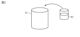
- 2-propanol is charged as the solvent 82 into the reaction vessel 81.
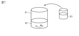
- a catalyst charging step S14 is performed.
- FIG. 7 in the catalyst charging step S14, first, stirring of the solvent 82 in the reaction vessel 81 is started. Then, aqueous ammonia is poured into the reaction vessel 81 as an aqueous solution 83 containing a catalyst.
- the catalyst in this embodiment is a hydroxide ion, and functions as a catalyst that promotes the hydrolysis of metal alkoxide 85, which will be described later.
- an element loading step S15 is performed. As shown in FIG. 8, in the element loading step S15, the plurality of elements 20 previously formed in the R-chamfering step S12 as described above are charged into the reaction container 81.
- a polymer charging step S16 is performed. As shown in FIG. 9, in the polymer charging step S16, polyvinylpyrrolidone is charged as the polymer 84 into the reaction container 81. As a result, the polymer 84 introduced into the reaction container 81 is adsorbed onto the outer surface 21 of the element body 20 .
- a metal alkoxide charging step S17 is performed.
- liquid tetraethyl orthosilicate is charged as the metal alkoxide 85 into the reaction vessel 81.
- tetraethyl orthosilicate is sometimes called tetraethoxysilane.
- the amount of metal alkoxide 85 introduced in the metal alkoxide introduction step S17 is calculated based on the area of the outer surface 21 of the element body 20 introduced in the element body introduction step S15. Specifically, it is calculated by multiplying the amount of metal alkoxide 85 per element body 20 necessary to form the glass film 50 covering the outer surface 21 of the element body 20 by the number of element bodies 20. .
- a film forming step S18 is performed.
- the stirring of the solvent 82 started in the above-mentioned solvent charging step S13 is continued for a predetermined period of time after the metal alkoxide 85 is charged into the reaction vessel 81 in the metal alkoxide charging step S17.
- the glass film 50 is formed by a liquid phase reaction within the reaction vessel 81.
- a drying step S19 is performed.
- the element body 20 is taken out from the reaction vessel 81 and dried.
- the sol-like glass film 50 is dried and becomes a gel-like glass film 50.
- a conductor coating step S20 is performed.
- two parts of the surface of the glass film 50 are formed: a part including a part covering the first end face 22A of the element body 20, and a part including a part covering the second end face 22B of the element body 20.
- a curing step S21 is performed. Specifically, in the curing step S21, the glass film 50 and the element body 20 coated with the conductive paste are heated. As a result, the water and polymer 84 are vaporized from the gel-like glass film 50, so that the glass film 50 covering the outer surface 21 of the element body 20 is fired and hardened. Furthermore, in the curing step S21, the conductor paste applied in the conductor coating step S20 is fired, thereby forming the first base electrode 61A and the second base electrode 62A.
- the glass film 50 has a part that touches Ag included in the first base electrode 61A and the second base electrode 62A, and a part that touches the glass included in the first base electrode 61A and the second base electrode 62A. There is a mixture of.
- the glass film 50 is integrated with the glass included in the first base electrode 61A and the second base electrode 62A. At this time, the glass film 50 is attracted to the glass contained in the first base electrode 61A and the second base electrode 62A. Therefore, on the outer surface 21 of the element body 20, the thickness TG of the glass film 50 becomes uneven.
- the molecular structure of MnAgO 2 included in the reaction layer 25 has a larger volume per molecule structure than the molecular structures of Mn 3 O 4 and Mn 2 NiO 4 included in the element body 20. That is, in the process of generating the reaction layer 25 in the element body 20, the volume of the reaction layer 25 expands, and stress is generated within the reaction layer 25. Then, the ionic bond between the metal atom and the oxygen atom in the MnAgO 2 of the reaction layer 25 is broken due to the stress. As the cutting of the molecular structure propagates starting from the point where the bond is cut, a void 26 is formed inside the reaction layer 25 .
- the first base electrode 61A side containing silver is caused by the Kirkendall effect caused by the difference in diffusion rate between the first internal electrode 41 and the first base electrode 61A.
- palladium contained on the first internal electrode 41 side is attracted.
- the first penetrating portion 71 extends through the glass film 50 from the first internal electrode 41 toward the first base electrode 61A, thereby connecting the first internal electrode 41 and the first base electrode 61A.
- the second through portion 72 that connects the second internal electrode 42 and the second base electrode 62A.
- a plating step S22 is performed. Electroplating is performed on the first base electrode 61A and the second base electrode 62A. As a result, a first metal layer 61B is formed on the surface of the first base electrode 61A. Further, a second metal layer 62B is formed on the surface of the second base electrode 62A. Although not shown, the first metal layer 61B and the second metal layer 62B are electroplated with two types of metal, nickel and tin, so that they have a two-layer structure. In this way, electronic component 10 is formed.
- the element body 20 has the reaction layer 25, and the reaction layer 25 has the voids 26.
- This gap 26 functions as a space that buffers force when force is applied to the electronic component 10 from the outside.
- this reaction layer 25 is located in a location where cracks and the like of the glass film 50 are likely to occur, that is, in the vicinity of the end ROI of each base electrode in the element body 20. This makes it possible to prevent cracks and the like from occurring in the glass film 50 near the end ROIs of the first base electrode 61A and the second base electrode 62A.
- the first base electrode 61A and the second base electrode 62A contain Ag as a conductive metal, and the element body 20 contains one or more of Mn 3 O 4 and Mn 2 NiO 4 . Containing Mn oxide, the reaction layer 25 is MnAgO2 .
- MnAgO 2 is generated in the Mn oxide. This changes the molecular structure and increases the volume of the reaction layer 25 compared to before the reaction. Then, strain occurs within the reaction layer 25, and the bond between Ag and O is broken. That is, according to the element body 20, the first base electrode 61A, and the second base electrode 62A having the above compositions, the voids 26 can be easily provided in the reaction layer 25.
- the acute angle between the longest straight line connecting two points on the outer peripheral edge of the void 26 and the outer surface 27 of the reaction layer 25 is 0° or more and 45° or less. . That is, the void 26 extends generally along the outer surface 27.
- the stress generated on the outer surface 21 of the element body 20 tends to act in a direction perpendicular to the outer surface 27 of the reaction layer 25.
- the voids 26 extending along the outer surface 27 have a higher impact buffering effect. Therefore, the impact on the glass film 50 can be efficiently alleviated.
- the ratio of the total volume of the voids 26 existing in the reaction layer 25 to the total volume of the reaction layer 25 is 0.1% or more and 5% or less.
- the porosity is less than 0.1%, it is difficult to disperse stress generated in the end ROI. Therefore, when stress concentrates on the end ROI, cracks and the like are likely to occur in the glass film 50.
- the porosity is greater than 5%, when moisture or gas enters the boundary between the element body 20 and the glass film 50, the path for moisture or gas to enter the element body 20 becomes wider. In other words, the durability of the element body 20 against moisture and gas tends to decrease. Therefore, by setting the porosity to 0.1% or more and 5% or less, stress concentrated on the end ROI can be dispersed while suppressing a decrease in the durability of the element body 20 against moisture and gas.
- the thickness TR of the reaction layer 25 is 50 nm or more and 500 nm or less. If the reaction layer 25 is less than 50 nm thick, it is difficult to disperse stress generated in the end ROI. Therefore, when stress concentrates on the end ROI, cracks and the like are likely to occur in the glass film 50. On the other hand, when the thickness TR of the reaction layer 25 is greater than 500 nm, when moisture or gas enters the boundary between the element body 20 and the glass film 50, the moisture or gas tends to penetrate deeply into the interior of the element body 20. As a result, the durability of the element body 20 tends to decrease. Therefore, by setting the thickness TR of the reaction layer 25 to 50 nm or more and 500 nm or less, stress concentrated on the end ROI can be dispersed while suppressing a decrease in durability of the element body 20.
- the thickness TG of the glass film 50 is 30 nm or more and 200 nm or less.
- the thickness TR of the reaction layer 25 increases. Then, when moisture or gas enters the boundary between the element body 20 and the glass film 50, the moisture or gas easily penetrates deep into the element body 20. As a result, the durability of the element body 20 tends to decrease.
- the thickness TG of the glass film 50 When the thickness TG of the glass film 50 is thicker than 200 nm, the conductive metal contained in the first base electrode 61A and the second base electrode 62A is difficult to diffuse into the element body 20. In other words, since the thickness TR of the reaction layer 25 becomes smaller, it is difficult to disperse stress. Therefore, when stress concentrates on the end ROI, cracks and the like are likely to occur in the glass film 50. Therefore, by setting the thickness TG of the glass film 50 to 30 nm or more and 200 nm or less, the reaction layer 25 with a suitable thickness TR can be formed.
- the electronic component 10 is not limited to a negative characteristic thermistor component.
- the electronic component 10 may be a thermistor component with a non-negative characteristic, a multilayer capacitor component, or an inductor component.
- the outer surface 21 of the element body 20 does not need to have the boundary surface 23 and the corner surface 24.
- the boundary surface 23 and the corner surface 24 may not exist.
- the element body 20 may contain Mn oxides other than Mn 3 O 4 and Mn 2 NiO 4 .
- the shapes of the first internal electrode 41 and the second internal electrode 42 are not limited as long as they can ensure electrical continuity with the corresponding first external electrode 61 and second external electrode 62.
- the number of the first internal electrodes 41 and the second internal electrodes 42 does not matter, and the number of internal electrodes may be one or three or more.
- the configuration of the first external electrode 61 is not limited to the example of the above embodiment.
- the first external electrode 61 may be composed only of the first base electrode 61A, and the first metal layer 61B may not have a two-layer structure. The same applies to the second external electrode 62 in this respect.
- the combination of materials for the first internal electrode 41 and the first base electrode 61A is not limited to the combination of palladium and silver.
- it may be a combination of copper and nickel, copper and silver, silver and gold, nickel and cobalt, or nickel and gold.
- one may be silver and the other may be a combination of silver and palladium.
- one may be a combination of palladium and the other of silver and palladium, or one may be copper and the other a combination of silver and palladium.
- one may be gold and the other may be a combination of silver and palladium.
- the first internal electrode 41 may be processed to be exposed before the external electrode forming step. For example, a portion of the glass film 50 may be physically removed by polishing the first end surface 22A side of the element body 20. Thereafter, by performing a base electrode forming step, the first internal electrode 41 and the first base electrode 61A can be connected. For example, after forming the first base electrode 61A, the glass film 50 may be formed including the surface of the first base electrode 61A, and the glass film 50 covering the surface of the first base electrode 61A may be removed. The same applies to the combination of materials for the second internal electrode 42 and the second base electrode 62A.
- the arrangement location of the first external electrode 61 is not limited to the example of the above embodiment.
- the first external electrode 61 may be arranged only on the first end surface 22A and one side surface 22C.
- the conductive metal included in the first base electrode 61A and the second base electrode 62A is not limited to Ag.
- Au, Cu, etc. may be used.
- the first base electrode 61A and the second base electrode 62A may contain two or more conductive metals. Note that if the conductive metal contained in the first base electrode 61A and the second base electrode 62A is Cu, the reaction layer 25 will contain MnCuO 2 as a composite oxide. In the case of this modification, the same effect as (2) described above can be obtained.
- the first base electrode 61A contains conductive metal and glass
- a part of the first base electrode 61A, including the edge may be composed only of glass without containing any metal component.
- the glass component contained in the first base electrode 61A and the glass film 50 may be fused, and the two may not have a clear boundary. Therefore, even if a portion including the edge of the first base electrode 61A is made only of glass without containing any metal component, the end of the metal component of the first base electrode 61A is defined as the edge E1. . In this respect, the same applies to the second base electrode 62A.
- the conductive metal contained in the first base electrode 61A and the second base electrode 62A may not be the same.
- the first base electrode 61A may contain Ag
- the second base electrode 62A may contain Cu.
- the glass film 50 does not need to cover the entire area of the outer surface 21 of the element body 20; it is only necessary that the first base electrode 61A and the second base electrode 62A cover the glass film 50.
- the range covered by the glass film 50 may be changed as appropriate in accordance with the shape of the element body 20, the positions of the first external electrode 61 and the second external electrode 62, and the like.
- the thickness TG of the glass film 50 in the direction perpendicular to the outer surface 21 of the element body 20 may be less than 30 nm or larger than 200 nm.
- the reaction layer 25 may contain both MnAgO 2 and MnCuO 2 as complex oxides, or may additionally contain complex oxides other than those mentioned above.
- the thickness TR of the reaction layer 25 in the direction perpendicular to the outer surface 21 of the element body 20 may be less than 50 nm or larger than 500 nm.
- the ratio of the total volume of the voids 26 existing in the reaction layer 25 to the total volume of the reaction layer 25 may be less than 0.1% or more than 5%.
- the acute angle formed between the longest straight line connecting two points on the outer peripheral edge of the void 26 and the outer surface 27 of the reaction layer 25 may be larger than 45°. Regardless of the direction in which the void 26 extends, the impact buffering effect of the void 26 can be obtained.
- (1) comprising an element body, a glass film covering the outer surface of the element body, and a base electrode covering a part of the outer surface of the glass film,
- the element body contains Mn oxide
- the base electrode contains a conductive metal and a glass component
- the element body has a reaction layer containing a composite oxide of Mn and the conductive metal at a location where the end portion of the base electrode contacts,
- the reaction layer is an electronic component having voids.
- the base electrode contains Ag as the conductive metal
- the element body contains one or more selected from Mn 3 O 4 and Mn 2 NiO 4 as the Mn oxide,
- the base electrode contains Cu as the conductive metal
- the element body contains one or more selected from Mn 3 O 4 and Mn 2 NiO 4 as the Mn oxide,
- the acute angle formed between the longest straight line connecting two points on the outer periphery of the void and the outer surface of the reaction layer is 0° or more and 45° or less.
- the electronic component according to any one of (1) to (4), wherein the ratio of the total volume of the voids present in the reaction layer to the total volume of the reaction layer is 0.1% or more and 5% or less. Electronic components listed.
Landscapes
- Engineering & Computer Science (AREA)
- Microelectronics & Electronic Packaging (AREA)
- Physics & Mathematics (AREA)
- Electromagnetism (AREA)
- Coils Or Transformers For Communication (AREA)
Abstract
An electronic component (10) comprises: an element body (20); a glass film (50) that covers the outer surface (21) of the element body (20); and a base electrode that covers a portion of the surface of the glass film (50). The element body (20) includes a Mn oxide. The base electrode includes a conductive metal and a glass component. Accordingly, the element body (20) has a reaction layer (25) that includes a composite oxide of Mn and a conductive metal, at the end of the base electrode. The reaction layer (25) has gaps (26).
Description
本開示は、電子部品に関する。
The present disclosure relates to electronic components.
特許文献1に記載の電子部品は、素体と、ガラス膜と、下地電極と、を備えている。素体は、セラミックスからなる。ガラス膜は、素体の外表面を覆っている。下地電極は、ガラス膜の外表面の一部を覆っている。なお、下地電極は、素体内部の内部電極と電気的に接続している。
The electronic component described in Patent Document 1 includes an element body, a glass film, and a base electrode. The element body is made of ceramics. A glass film covers the outer surface of the element body. The base electrode covers a portion of the outer surface of the glass film. Note that the base electrode is electrically connected to an internal electrode inside the element body.
特許文献1に記載されたような電子部品において、電子部品に外部から力が加わると、ガラス膜にクラック等が生じることがある。ガラス膜にクラック等が生じると、水分等がクラック等を通じて素体へと浸入するおそれがある。特に、ガラス膜のなかでも、下地電極に覆われている部分と覆われていない部分との境界近傍では、クラック等が発生しやすい。
In electronic components such as those described in Patent Document 1, when force is applied to the electronic component from the outside, cracks or the like may occur in the glass film. If cracks or the like occur in the glass film, there is a risk that moisture or the like may infiltrate into the element body through the cracks or the like. In particular, cracks are likely to occur in the glass film near the boundary between the portion covered by the base electrode and the portion not covered.
本開示の一態様に係る電子部品は、素体と、前記素体の外表面を覆うガラス膜と、前記ガラス膜の外表面の一部を覆う下地電極と、を備え、前記素体はMn酸化物を含み、前記下地電極は導電性金属及びガラス成分を含み、前記素体は、前記下地電極の端部が接触する箇所に、Mn及び前記導電性金属の複合酸化物を含む反応層を有しており、前記反応層は空隙を有する。
An electronic component according to one aspect of the present disclosure includes an element body, a glass film that covers an outer surface of the element body, and a base electrode that covers a part of the outer surface of the glass film, and the element body has Mn. oxide, the base electrode includes a conductive metal and a glass component, and the element body includes a reaction layer containing a composite oxide of Mn and the conductive metal at a location where an end of the base electrode contacts. The reaction layer has voids.
上記構成によれば、素体は、反応層を有し、且つ反応層は空隙を有する。この空隙が、電子部品に対して外部から力が加わったときに、力を緩衝する空間として機能する。しかも、この反応層は、ガラス膜のクラック等が生じやすい箇所に位置している。これにより、下地電極の端縁の近傍においてガラス膜のクラック等の発生を防止できる。
According to the above configuration, the element body has a reaction layer, and the reaction layer has voids. This gap functions as a space that buffers force when force is applied to the electronic component from the outside. Moreover, this reaction layer is located at a location where cracks in the glass film are likely to occur. This can prevent the occurrence of cracks in the glass film near the edges of the base electrode.
下地電極に覆われている部分と覆われていない部分との境界近傍におけるガラス膜のクラック等の発生を防止できる。
It is possible to prevent the occurrence of cracks in the glass film near the boundary between the portion covered by the base electrode and the portion not covered.
<電子部品の一実施形態>
以下、電子部品の一実施形態を、図面を参照して説明する。なお、図面は、理解を容易にするために構成要素を拡大して示している場合がある。構成要素の寸法比率は実際のものと、又は別の図面中のものと異なる場合がある。 <One embodiment of electronic component>
Hereinafter, one embodiment of the electronic component will be described with reference to the drawings. Note that in the drawings, components may be shown enlarged to facilitate understanding. The dimensional proportions of the components may differ from those in reality or from those in different drawings.
(全体構成について)
図1に示すように、電子部品10は、例えば、回路基板等に実装される表面実装型の負特性サーミスタ部品である。なお、負特性サーミスタ部品は、温度が上がると抵抗値が下がるという特性を有するものである。 (About the overall structure)
As shown in FIG. 1, theelectronic component 10 is, for example, a surface-mounted negative temperature coefficient thermistor component mounted on a circuit board or the like. Note that the negative characteristic thermistor component has a characteristic that the resistance value decreases as the temperature increases.
図1に示すように、電子部品10は、例えば、回路基板等に実装される表面実装型の負特性サーミスタ部品である。なお、負特性サーミスタ部品は、温度が上がると抵抗値が下がるという特性を有するものである。 (About the overall structure)
As shown in FIG. 1, the
電子部品10は、素体20を備えている。素体20は、略四角柱状であり、中心軸線CAを有する。なお、以下では、中心軸線CAに沿って延びる軸を第1軸Xとする。また、第1軸Xに直交する軸の1つを第2軸Yとする。そして、第1軸X及び第2軸Yに直交する軸を第3軸Zとする。さらに、第1軸Xに沿う方向の一方を第1正方向X1とし、第1軸Xに沿う方向のうち第1正方向X1と反対方向を第1負方向X2とする。また、第2軸Yに沿う方向の一方を第2正方向Y1とし、第2軸Yに沿う方向のうち第2正方向Y1と反対方向を第2負方向Y2とする。さらに、第3軸Zに沿う方向の一方を第3正方向Z1とし、第3軸Zに沿う方向のうち第3正方向Z1と反対方向を第3負方向Z2とする。
The electronic component 10 includes an element body 20. The element body 20 has a substantially quadrangular prism shape and has a central axis CA. Note that, hereinafter, the axis extending along the central axis CA will be referred to as a first axis X. Furthermore, one of the axes orthogonal to the first axis X is defined as a second axis Y. Then, an axis perpendicular to the first axis X and the second axis Y is defined as a third axis Z. Furthermore, one of the directions along the first axis X is defined as a first positive direction X1, and among the directions along the first axis X, the opposite direction to the first positive direction X1 is defined as a first negative direction X2. Further, one of the directions along the second axis Y is defined as a second positive direction Y1, and the direction opposite to the second positive direction Y1 among the directions along the second axis Y is defined as a second negative direction Y2. Furthermore, one of the directions along the third axis Z is defined as a third positive direction Z1, and among the directions along the third axis Z, the direction opposite to the third positive direction Z1 is defined as a third negative direction Z2.
素体20の外表面21は、6個の平面22を有している。なお、ここでいう素体20の「面」とは、素体20全体を観察したときに面として観察できるものをいう。つまり、例えば素体20の一部を顕微鏡等で拡大して観察しなければわからないような微小な凹凸、段差が存在しても、平面又は曲面と表現する。6個の平面22は、互いに異なる方向を向いている。6個の平面22は、第1正方向X1を向く第1端面22Aと、第1負方向X2を向く第2端面22Bと、4つの側面22Cとに大別される。4つの側面22Cは、第3正方向Z1を向く面と、第3負方向Z2を向く面と、第2正方向Y1を向く面と、第2負方向Y2を向く面と、である。
The outer surface 21 of the element body 20 has six flat surfaces 22. Note that the "surface" of the element body 20 herein refers to what can be observed as a surface when the entire element body 20 is observed. That is, even if there are minute irregularities or steps that cannot be seen unless a part of the element body 20 is observed under a microscope or the like, it is expressed as a flat or curved surface. The six planes 22 face different directions. The six planes 22 are roughly divided into a first end surface 22A facing the first positive direction X1, a second end surface 22B facing the first negative direction X2, and four side surfaces 22C. The four side surfaces 22C are a surface facing the third positive direction Z1, a surface facing the third negative direction Z2, a surface facing the second positive direction Y1, and a surface facing the second negative direction Y2.
素体20の外表面21は、12個の境界面23を有している。境界面23は、隣り合う平面22同士の境界に存在する曲面を含んでいる。すなわち、境界面23は、例えば、隣り合う平面22によって形成される角をR面取り加工することで形成される曲面を含んでいる。
The outer surface 21 of the element body 20 has 12 boundary surfaces 23. The boundary surface 23 includes a curved surface existing at the boundary between adjacent planes 22. That is, the boundary surface 23 includes, for example, a curved surface formed by rounding the corner formed by the adjacent planes 22.
また、素体20の外表面21は、8個の球面状のコーナ面24を有している。コーナ面24は、隣り合う3つの平面22同士の境界部分である。換言すれば、コーナ面24は、3つの境界面23が交わる箇所の曲面を含んでいる。すなわち、コーナ面24は、例えば、隣り合う3つの平面22によって形成される角をR面取り加工することによって形成された曲面を含んでいる。なお、図1では、後述するガラス膜50の表面を素体20の外表面21と同一視して符号を付している。
Further, the outer surface 21 of the element body 20 has eight spherical corner surfaces 24. The corner surface 24 is a boundary between three adjacent planes 22. In other words, the corner surface 24 includes a curved surface where the three boundary surfaces 23 intersect. That is, the corner surface 24 includes a curved surface formed by, for example, rounding the corner formed by the three adjacent planes 22. In FIG. 1, the surface of a glass film 50, which will be described later, is identified with the outer surface 21 of the element body 20 and is designated by a reference numeral.
図1に示すように、素体20は、第1軸Xに沿う方向の寸法が、第3軸Zに沿う方向の寸法よりも大きい。また、素体20は、第1軸Xに沿う方向の寸法が、第2軸Yに沿う方向の寸法よりも大きい。素体20の材質は、金属酸化物を焼成したセラミックスである。具体的には、素体20は、Mn酸化物として、Mn3O4及びMn2NiO4から選ばれる1以上を含んでいる。
As shown in FIG. 1, the dimension of the element body 20 in the direction along the first axis X is larger than the dimension in the direction along the third axis Z. Furthermore, the dimension of the element body 20 in the direction along the first axis X is larger than the dimension in the direction along the second axis Y. The material of the element body 20 is ceramics made of fired metal oxide. Specifically, the element body 20 contains one or more selected from Mn 3 O 4 and Mn 2 NiO 4 as the Mn oxide.
図2に示すように、電子部品10は、2つの第1内部電極41と、2つの第2内部電極42と、を備えている。第1内部電極41及び第2内部電極42は、素体20の内部に埋め込まれている。
As shown in FIG. 2, the electronic component 10 includes two first internal electrodes 41 and two second internal electrodes 42. The first internal electrode 41 and the second internal electrode 42 are embedded inside the element body 20 .
第1内部電極41の材質は、導電性の材料である。例えば、第1内部電極41の材質は、パラジウムである。また、第2内部電極42の材質は、第1内部電極41の材質と同一である。
The material of the first internal electrode 41 is a conductive material. For example, the material of the first internal electrode 41 is palladium. Further, the material of the second internal electrode 42 is the same as that of the first internal electrode 41.
第1内部電極41の形状は、長方形板状である。第1内部電極41の主面は、第2軸Yに直交している。第2内部電極42の形状は、第1内部電極41と同じ長方形板状である。第2内部電極42の主面は、第1内部電極41と同様に、第2軸Yに直交している。
The shape of the first internal electrode 41 is a rectangular plate. The main surface of the first internal electrode 41 is perpendicular to the second axis Y. The shape of the second internal electrode 42 is the same rectangular plate shape as the first internal electrode 41. The main surface of the second internal electrode 42 is perpendicular to the second axis Y, similarly to the first internal electrode 41.
第1内部電極41の第1軸Xに沿う方向の寸法は、素体20の第1軸Xに沿う方向の寸法より小さくなっている。また、図1に示すように、第1内部電極41の第3軸Zに沿う方向の寸法は、素体20の第3軸Zに沿う方向の寸法の略3分の2となっている。第2内部電極42の各方向の寸法は、第1内部電極41と同じ寸法となっている。
The dimension of the first internal electrode 41 in the direction along the first axis X is smaller than the dimension of the element body 20 in the direction along the first axis X. Further, as shown in FIG. 1, the dimension of the first internal electrode 41 in the direction along the third axis Z is approximately two-thirds of the dimension of the element body 20 in the direction along the third axis Z. The dimensions of the second internal electrode 42 in each direction are the same as those of the first internal electrode 41.
図2に示すように、第1内部電極41と第2内部電極42とは、第2軸Yに沿う方向に互い違いに位置している。すなわち、第2正方向Y1を向く側面22Cから第2負方向Y2に向かって、第1内部電極41、第2内部電極42、第1内部電極41、第2内部電極42の順に並んでいる。この実施形態では、各内部電極間の第2軸Yに沿う方向の距離は、等しくなっている。
As shown in FIG. 2, the first internal electrodes 41 and the second internal electrodes 42 are located alternately in the direction along the second axis Y. That is, the first internal electrode 41, the second internal electrode 42, the first internal electrode 41, and the second internal electrode 42 are arranged in this order from the side surface 22C facing the second positive direction Y1 toward the second negative direction Y2. In this embodiment, the distance between each internal electrode in the direction along the second axis Y is equal.
図1に示すように、2つの第1内部電極41及び2つの第2内部電極42は、いずれも、第3軸Zに沿う方向において、素体20の中央に位置している。その一方で、図2に示すように、第1内部電極41は、第1正方向X1に寄って位置している。第2内部電極42は、第1負方向X2に寄って位置している。
As shown in FIG. 1, the two first internal electrodes 41 and the two second internal electrodes 42 are both located at the center of the element body 20 in the direction along the third axis Z. On the other hand, as shown in FIG. 2, the first internal electrode 41 is located closer to the first positive direction X1. The second internal electrode 42 is located closer to the first negative direction X2.
具体的には、第1内部電極41の第1正方向X1側の端は、素体20の第1正方向X1側の端と一致している。第1内部電極41の第1負方向X2側の端は、素体20の内部に位置しており、素体20の第1負方向X2側の端にまで至っていない。一方で、第2内部電極42の第1負方向X2側の端は、素体20の第1負方向X2側の端と一致している。第2内部電極42の第1正方向X1側の端は、素体20の内部に位置しており、素体20の第1正方向X1側の端にまで至っていない。
Specifically, the end of the first internal electrode 41 on the first positive direction X1 side matches the end of the element body 20 on the first positive direction X1 side. The end of the first internal electrode 41 on the first negative direction X2 side is located inside the element body 20 and does not reach the end of the element body 20 on the first negative direction X2 side. On the other hand, the end of the second internal electrode 42 on the first negative direction X2 side coincides with the end of the element body 20 on the first negative direction X2 side. The end of the second internal electrode 42 on the first positive direction X1 side is located inside the element body 20 and does not reach the end of the element body 20 on the first positive direction X1 side.
図2に示すように、電子部品10は、ガラス膜50を備えている。ガラス膜50は、素体20の外表面21を覆っている。ガラス膜50の主な材質は、絶縁性のガラスである。したがって、ガラス膜50は、二酸化ケイ素を含んでいる。なお、ガラス膜50の詳細については後述する。
As shown in FIG. 2, the electronic component 10 includes a glass film 50. Glass film 50 covers outer surface 21 of element body 20 . The main material of the glass film 50 is insulating glass. Therefore, the glass film 50 contains silicon dioxide. Note that details of the glass film 50 will be described later.
電子部品10は、第1外部電極61と、第2外部電極62と、を備えている。第1外部電極61は、第1下地電極61Aと、第1金属層61Bと、を有している。第1下地電極61Aは、素体20の外表面21のうち、第1端面22Aを含む一部分において、ガラス膜50の上から積層されている。具体的には、第1下地電極61Aは、素体20の第1端面22Aと、4つの側面22Cの第1正方向X1側の一部を覆う、5面電極である。この第1下地電極61Aの材質は、導電性金属及びガラスの混合物である。具体的には、第1下地電極61Aの材質は、Ag及びガラスの混合物である。
The electronic component 10 includes a first external electrode 61 and a second external electrode 62. The first external electrode 61 includes a first base electrode 61A and a first metal layer 61B. The first base electrode 61A is laminated on the glass film 50 on a portion of the outer surface 21 of the element body 20 including the first end surface 22A. Specifically, the first base electrode 61A is a five-sided electrode that covers the first end surface 22A of the element body 20 and a portion of the four side surfaces 22C on the first positive direction X1 side. The material of this first base electrode 61A is a mixture of conductive metal and glass. Specifically, the material of the first base electrode 61A is a mixture of Ag and glass.
第1金属層61Bは、第1下地電極61Aを外部から覆っている。そのため、第1金属層61Bは、第1下地電極61Aに積層されている。図示は省略するが、第1金属層61Bは、第1下地電極61A側から順に、ニッケル層と、錫層と、の2層構造となっている。
The first metal layer 61B covers the first base electrode 61A from the outside. Therefore, the first metal layer 61B is laminated on the first base electrode 61A. Although not shown, the first metal layer 61B has a two-layer structure including a nickel layer and a tin layer in order from the first base electrode 61A side.
第2外部電極62は、第2下地電極62Aと、第2金属層62Bと、を有している。第2下地電極62Aは、素体20の外表面21のうち、第2端面22Bを含む一部分において、ガラス膜50の上から積層されている。具体的には、第2下地電極62Aは、素体20の第2端面22Bと、4つの側面22Cの第1負方向X2側の一部を覆う、5面電極である。この第2下地電極62Aの材質は、第1下地電極61Aの材質と同じである。すなわち、第2下地電極62Aの材質は、Ag及びガラスの混合物である。
The second external electrode 62 includes a second base electrode 62A and a second metal layer 62B. The second base electrode 62A is laminated on the glass film 50 on a portion of the outer surface 21 of the element body 20, including the second end surface 22B. Specifically, the second base electrode 62A is a five-sided electrode that covers the second end surface 22B of the element body 20 and a portion of the four side surfaces 22C on the first negative direction X2 side. The material of this second base electrode 62A is the same as the material of the first base electrode 61A. That is, the material of the second base electrode 62A is a mixture of Ag and glass.
第2金属層62Bは、第2下地電極62Aを外部から覆っている。そのため、第2金属層62Bは、第2下地電極62Aに積層されている。具体的には、第2金属層62Bは、第1金属層61Bと同様に、ニッケル層と、錫層と、の2層構造となっている。
The second metal layer 62B covers the second base electrode 62A from the outside. Therefore, the second metal layer 62B is laminated on the second base electrode 62A. Specifically, the second metal layer 62B has a two-layer structure of a nickel layer and a tin layer, similar to the first metal layer 61B.
第2外部電極62は、側面22C上において、第1外部電極61にまでは至っておらず、第1外部電極61に対して第1軸Xに沿う方向に離れて配置されている。そして、素体20の側面22C上において、第1軸Xに沿う方向の中央部分は、第1外部電極61及び第2外部電極62が積層されておらず、ガラス膜50が露出している。なお、図1及び図2では、第1外部電極61及び第2外部電極62は、二点鎖線で図示している。
The second external electrode 62 does not reach the first external electrode 61 on the side surface 22C, and is arranged apart from the first external electrode 61 in the direction along the first axis X. On the side surface 22C of the element body 20, the first external electrode 61 and the second external electrode 62 are not stacked at the central portion in the direction along the first axis X, and the glass film 50 is exposed. In addition, in FIG. 1 and FIG. 2, the first external electrode 61 and the second external electrode 62 are illustrated by two-dot chain lines.
第1外部電極61と第1内部電極41における第1正方向X1側の端とは、ガラス膜50を貫通する第1貫通部71を介して接続している。なお、詳細は後述するが、第1貫通部71は、電子部品10の製造過程において、第1内部電極41を構成するパラジウムが第1外部電極61側へと延びることによって形成される。
The first external electrode 61 and the end of the first internal electrode 41 on the first positive direction X1 side are connected via a first penetration portion 71 that penetrates the glass film 50. Although details will be described later, the first penetrating portion 71 is formed by palladium forming the first internal electrode 41 extending toward the first external electrode 61 during the manufacturing process of the electronic component 10.
また、第2外部電極62と第2内部電極42における第1負方向X2側の端とは、ガラス膜50を貫通する第2貫通部72を介して接続している。第2貫通部72も、第1貫通部71と同様に、電子部品10の製造過程において、第2内部電極42を構成するパラジウムが第2外部電極62側へと延びることによって形成される。なお、図2では、第1内部電極41と第1貫通部71とを境界のある別の部材として図示しているが、実際には両者の間に明確な境界は存在しない。この点、第2貫通部72についても同様である。また、図1においては、第1貫通部71及び第2貫通部72の図示を省略する。
Furthermore, the second external electrode 62 and the end of the second internal electrode 42 on the first negative direction X2 side are connected via a second penetration portion 72 that penetrates the glass film 50. Similarly to the first penetration part 71, the second penetration part 72 is also formed by palladium forming the second internal electrode 42 extending toward the second external electrode 62 during the manufacturing process of the electronic component 10. Although FIG. 2 shows the first internal electrode 41 and the first penetration part 71 as separate members with a boundary, there is actually no clear boundary between them. The same applies to the second penetrating portion 72 in this respect. Moreover, in FIG. 1, illustration of the first penetration part 71 and the second penetration part 72 is omitted.
(ガラス膜について)
ガラス膜50は、素体20の外表面21の略すべての領域を覆っている。具体的には、ガラス膜50は、素体20に第1下地電極61A及び第2下地電極62Aが積層されていない箇所においては、素体20の外表面21のすべての領域を覆っている。その一方で、ガラス膜50は、素体20に第1下地電極61A及び第2下地電極62Aが積層されている箇所においては、部分的に途切れている。このようにガラス膜50が途切れている箇所においては、第1下地電極61A及び第2下地電極62Aは、素体20の外表面21に、直接に接触している。換言すると、第1下地電極61A及び第2下地電極62Aは、ガラス膜50の一部及び素体20の外表面21におけるガラス膜50によって覆われていない部分を覆っている。すなわち、第1下地電極61A及び第2下地電極62Aは、ガラス膜50の一部だけでなく、素体20の外表面21におけるガラス膜50が途切れることで露出した部分も覆っている。なお、図2では、説明の便宜上、ガラス膜50が途切れた部分(第1下地電極61A及び第2下地電極62Aが素体20の外表面21を覆っている部分)の図示を省略している。第1下地電極61A及び第2下地電極62Aに覆われていない箇所では、ガラス膜50における素体20の外表面21に垂直な方向での厚さTGは、30nm以上200nm以下である。なお、ガラス膜50の厚さTGは、異なる3点で測定した値の平均値とする。 (About glass membrane)
Theglass film 50 covers substantially all of the outer surface 21 of the element body 20 . Specifically, the glass film 50 covers the entire area of the outer surface 21 of the element body 20 in areas where the first base electrode 61A and the second base electrode 62A are not stacked on the element body 20. On the other hand, the glass film 50 is partially interrupted at a location where the first base electrode 61A and the second base electrode 62A are laminated on the element body 20. In such places where the glass film 50 is interrupted, the first base electrode 61A and the second base electrode 62A are in direct contact with the outer surface 21 of the element body 20. In other words, the first base electrode 61A and the second base electrode 62A cover a portion of the glass film 50 and a portion of the outer surface 21 of the element body 20 that is not covered by the glass film 50. That is, the first base electrode 61A and the second base electrode 62A cover not only a part of the glass film 50 but also the part exposed by the break in the glass film 50 on the outer surface 21 of the element body 20. In addition, in FIG. 2, for convenience of explanation, illustration of the part where the glass film 50 is interrupted (the part where the first base electrode 61A and the second base electrode 62A cover the outer surface 21 of the element body 20) is omitted. . At a portion not covered by the first base electrode 61A and the second base electrode 62A, the thickness TG of the glass film 50 in the direction perpendicular to the outer surface 21 of the element body 20 is 30 nm or more and 200 nm or less. Note that the thickness TG of the glass film 50 is an average value of values measured at three different points.
ガラス膜50は、素体20の外表面21の略すべての領域を覆っている。具体的には、ガラス膜50は、素体20に第1下地電極61A及び第2下地電極62Aが積層されていない箇所においては、素体20の外表面21のすべての領域を覆っている。その一方で、ガラス膜50は、素体20に第1下地電極61A及び第2下地電極62Aが積層されている箇所においては、部分的に途切れている。このようにガラス膜50が途切れている箇所においては、第1下地電極61A及び第2下地電極62Aは、素体20の外表面21に、直接に接触している。換言すると、第1下地電極61A及び第2下地電極62Aは、ガラス膜50の一部及び素体20の外表面21におけるガラス膜50によって覆われていない部分を覆っている。すなわち、第1下地電極61A及び第2下地電極62Aは、ガラス膜50の一部だけでなく、素体20の外表面21におけるガラス膜50が途切れることで露出した部分も覆っている。なお、図2では、説明の便宜上、ガラス膜50が途切れた部分(第1下地電極61A及び第2下地電極62Aが素体20の外表面21を覆っている部分)の図示を省略している。第1下地電極61A及び第2下地電極62Aに覆われていない箇所では、ガラス膜50における素体20の外表面21に垂直な方向での厚さTGは、30nm以上200nm以下である。なお、ガラス膜50の厚さTGは、異なる3点で測定した値の平均値とする。 (About glass membrane)
The
(反応層について)
図3に示すように、素体20は、反応層25を有している。反応層25は、素体20の外表面21を含む一部分である。すなわち、反応層25の外表面27は、素体20の外表面21の一部である。反応層25は、Mn及びAgの複合酸化物であるMnAgO2を含んでいる。換言すると、素体20のうち、MnAgO2を含んでいない箇所は、反応層25ではない。なお、この複合酸化物中のAgは、第1下地電極61A及び第2下地電極62Aに由来するものである。 (About the reaction layer)
As shown in FIG. 3, theelement body 20 has a reaction layer 25. Reaction layer 25 is a portion of element body 20 that includes outer surface 21 . That is, the outer surface 27 of the reaction layer 25 is a part of the outer surface 21 of the element body 20. The reaction layer 25 contains MnAgO 2 which is a composite oxide of Mn and Ag. In other words, a portion of the element body 20 that does not contain MnAgO 2 is not the reaction layer 25 . Note that Ag in this composite oxide originates from the first base electrode 61A and the second base electrode 62A.
図3に示すように、素体20は、反応層25を有している。反応層25は、素体20の外表面21を含む一部分である。すなわち、反応層25の外表面27は、素体20の外表面21の一部である。反応層25は、Mn及びAgの複合酸化物であるMnAgO2を含んでいる。換言すると、素体20のうち、MnAgO2を含んでいない箇所は、反応層25ではない。なお、この複合酸化物中のAgは、第1下地電極61A及び第2下地電極62Aに由来するものである。 (About the reaction layer)
As shown in FIG. 3, the
反応層25は、素体20のうち、第1下地電極61A及び第2下地電極62Aが接触する箇所に位置している。したがって、反応層25は、第1下地電極61Aの端部ROI及び第2下地電極62Aの端部ROIが接触する箇所にも存在する。なお、図3及び図4では、反応層25を断面視で四角形状に図示しているが、反応層25が断面視で楕円形状であったり四角形以外の多角形状であったりすることもある。
The reaction layer 25 is located in the element body 20 at a location where the first base electrode 61A and the second base electrode 62A are in contact. Therefore, the reaction layer 25 is also present at a location where the end ROI of the first base electrode 61A and the end ROI of the second base electrode 62A are in contact with each other. 3 and 4, the reaction layer 25 is shown to have a rectangular shape when viewed in cross section, but the reaction layer 25 may have an elliptical shape or a polygonal shape other than a quadrangle when viewed in cross section.
なお、第1下地電極61Aの端部ROIは、次のように定義される。先ず、電子部品10を中心軸線CAに平行な断面で断面視する。そして、当該断面上において、第1下地電極61Aの第1正方向X1側の端から、第1負方向X2側の端縁E1までの、中心軸線CAに沿う方向での全長を特定する。そして、第1下地電極61Aの端縁E1から、第1正方向X1に向かって、上記全長の5%の位置E2までの範囲を、第1下地電極61Aの端部ROIとする。このように、第1下地電極61Aの端部ROIとは、端縁E1から中心軸線CAに沿う方向の全長の5%の範囲である。この点、第2下地電極62Aについても同様である。
Note that the end ROI of the first base electrode 61A is defined as follows. First, the electronic component 10 is viewed in cross section parallel to the central axis CA. Then, on the cross section, the total length in the direction along the central axis CA from the end of the first base electrode 61A on the first positive direction X1 side to the end edge E1 on the first negative direction X2 side is specified. Then, the range from the edge E1 of the first base electrode 61A toward the first positive direction X1 to the position E2 of 5% of the total length is defined as the end ROI of the first base electrode 61A. In this way, the end ROI of the first base electrode 61A is a range of 5% of the total length in the direction along the central axis CA from the end edge E1. In this respect, the same applies to the second base electrode 62A.
図4に示すように、素体20の外表面21に垂直な方向での反応層25の厚さTRは、50nm以上500nm以下である。なお、反応層25の厚さTRは、次のように定義する。反応層25の外表面27の任意の一点と、その点から反応層25の外表面27に垂直な方向に直線を引いたときに、反応層25の外表面27とは反対側の面との交点との距離を、その任意の一点における反応層25の厚さとする。そして、1つの反応層25において3点で反応層25の厚さを測定する。これら3点での反応層25の厚さの平均値を、反応層25全体の厚さTRとする。
As shown in FIG. 4, the thickness TR of the reaction layer 25 in the direction perpendicular to the outer surface 21 of the element body 20 is 50 nm or more and 500 nm or less. Note that the thickness TR of the reaction layer 25 is defined as follows. When an arbitrary point on the outer surface 27 of the reaction layer 25 is drawn from that point in a direction perpendicular to the outer surface 27 of the reaction layer 25, the distance between an arbitrary point on the outer surface 27 of the reaction layer 25 and the surface opposite to the outer surface 27 of the reaction layer 25 Let the distance from the intersection point be the thickness of the reaction layer 25 at that arbitrary point. Then, the thickness of each reaction layer 25 is measured at three points. The average value of the thickness of the reaction layer 25 at these three points is defined as the thickness TR of the entire reaction layer 25.
反応層25は、複数の空隙26を有している。空隙26は、特定の方向に向かって長尺な形状になっている。そして、空隙26の向きは、概ね素体20の外表面21に沿っている。具体的には、素体20の外表面21に直交する断面で反応層25を観察したとき、空隙26の外周縁上の2点を結ぶ直線のうち最も長い直線を特定する。そして、この直線と反応層25の外表面27とのなす鋭角が、0°以上45°以下である。
The reaction layer 25 has a plurality of voids 26. The void 26 has an elongated shape in a specific direction. The direction of the void 26 is generally along the outer surface 21 of the element body 20. Specifically, when the reaction layer 25 is observed in a cross section perpendicular to the outer surface 21 of the element body 20, the longest straight line connecting two points on the outer periphery of the void 26 is identified. The acute angle between this straight line and the outer surface 27 of the reaction layer 25 is 0° or more and 45° or less.
また、反応層25の総体積に対する空隙26の総体積の割合を空隙率と定義する。この空隙率は、0.1%以上5%以下である。なお、空隙率は次のように算出する。まず、電子顕微鏡により、各下地電極の端部ROI及びその近傍の素体20の断面を撮影する。そして、撮影した画像において、反応層25の面積を求める。次に、当該画像において、空隙26の面積を求める。そして、素体20のうち、端部ROIに接する箇所の反応層25の面積の積算値を、反応層25の総体積とする。そして、各反応層25における空隙26の面積の積算値を、空隙26の総体積とする。そして、「空隙26の総体積/反応層25の総体積」に100を乗算したものが空隙率である。したがって、本実施形態においては、空隙率は、百分率で示される。
Furthermore, the ratio of the total volume of the voids 26 to the total volume of the reaction layer 25 is defined as the porosity. This porosity is 0.1% or more and 5% or less. Note that the porosity is calculated as follows. First, an electron microscope is used to photograph the end ROI of each base electrode and the cross section of the element body 20 in the vicinity thereof. Then, in the photographed image, the area of the reaction layer 25 is determined. Next, in the image, the area of the void 26 is determined. Then, the integrated value of the area of the reaction layer 25 at the portion of the element body 20 that is in contact with the end ROI is defined as the total volume of the reaction layer 25 . Then, the integrated value of the area of the voids 26 in each reaction layer 25 is taken as the total volume of the voids 26. The porosity is obtained by multiplying "total volume of voids 26/total volume of reaction layer 25" by 100. Therefore, in this embodiment, the porosity is expressed as a percentage.
(電子部品の製造方法について)
次に、電子部品10の製造方法について説明する。
図5に示すように、電子部品10の製造方法は、積層体準備工程S11と、R面取り加工工程S12と、溶媒投入工程S13と、触媒投入工程S14と、素体投入工程S15と、ポリマー投入工程S16と、金属アルコキシド投入工程S17と、を備えている。また、電子部品10の製造方法は、成膜工程S18と、乾燥工程S19と、導電体塗布工程S20と、硬化工程S21と、めっき工程S22と、をさらに備えている。 (About the manufacturing method of electronic components)
Next, a method for manufacturing theelectronic component 10 will be described.
As shown in FIG. 5, the method for manufacturing theelectronic component 10 includes a laminate preparation step S11, an R chamfering step S12, a solvent charging step S13, a catalyst charging step S14, an element charging step S15, and a polymer charging step S15. The method includes a step S16 and a metal alkoxide charging step S17. The method for manufacturing the electronic component 10 further includes a film forming step S18, a drying step S19, a conductor coating step S20, a curing step S21, and a plating step S22.
次に、電子部品10の製造方法について説明する。
図5に示すように、電子部品10の製造方法は、積層体準備工程S11と、R面取り加工工程S12と、溶媒投入工程S13と、触媒投入工程S14と、素体投入工程S15と、ポリマー投入工程S16と、金属アルコキシド投入工程S17と、を備えている。また、電子部品10の製造方法は、成膜工程S18と、乾燥工程S19と、導電体塗布工程S20と、硬化工程S21と、めっき工程S22と、をさらに備えている。 (About the manufacturing method of electronic components)
Next, a method for manufacturing the
As shown in FIG. 5, the method for manufacturing the
先ず、素体20を形成するにあたって、積層体準備工程S11では、境界面23及びコーナ面24を備えない素体20である積層体を準備する。すなわち、積層体は、R面取りする前の状態であり、6つの平面22を有する直方体状である。例えば、先ず、素体20となる複数のセラミックスのシートを準備する。当該シートは、薄い板状である。当該シート上に、第1内部電極41となる導電性ペーストを積層する。当該積層ペースト上に、素体20となるセラミックスのシートを積層する。当該シート上に、第2内部電極42となる導電性ペーストを積層する。このように、セラミックスのシートと導電性ペーストとを積層する。そして、所定のサイズにカットすることで、未焼成の積層体を形成する。その後、未焼成の積層体を高温で焼成することで、積層体を準備する。
First, in forming the element body 20, in a laminate preparation step S11, a laminate which is the element body 20 without the boundary surface 23 and the corner surface 24 is prepared. That is, the laminate is in a state before R-chamfering and is in the shape of a rectangular parallelepiped with six planes 22. For example, first, a plurality of ceramic sheets that will become the element body 20 are prepared. The sheet is in the form of a thin plate. A conductive paste that will become the first internal electrode 41 is laminated on the sheet. A ceramic sheet that will become the element body 20 is laminated on the lamination paste. A conductive paste that will become the second internal electrode 42 is laminated on the sheet. In this way, the ceramic sheet and the conductive paste are laminated. Then, by cutting to a predetermined size, an unfired laminate is formed. Thereafter, a laminate is prepared by firing the unfired laminate at a high temperature.
次に、図5に示すように、R面取り加工工程S12を行う。R面取り加工工程S12では、積層体準備工程S11で準備した積層体に対して境界面23及びコーナ面24を形成する。例えば、バレル研磨により、積層体の角がR面取り加工されることによって、曲面を有する境界面23及び曲面を有するコーナ面24が形成される。これにより、素体20が形成される。
Next, as shown in FIG. 5, an R chamfering step S12 is performed. In the R chamfering step S12, a boundary surface 23 and a corner surface 24 are formed on the laminate prepared in the laminate preparation step S11. For example, by barrel polishing, the corners of the laminate are rounded to form a curved boundary surface 23 and a curved corner surface 24 . Thereby, the element body 20 is formed.
次に、図5に示すように、溶媒投入工程S13を行う。図6に示すように、溶媒投入工程S13では、反応容器81内に、溶媒82として、2-プロパノールを投入する。
次に、図5に示すように、触媒投入工程S14を行う。図7に示すように、触媒投入工程S14では、先ず、反応容器81内の溶媒82の撹拌を開始する。そして、反応容器81内に、触媒を含む水溶液83として、アンモニア水を投入する。この実施形態における触媒は、水酸化物イオンであり、後述する金属アルコキシド85の加水分解を促進する触媒として機能する。 Next, as shown in FIG. 5, a solvent injection step S13 is performed. As shown in FIG. 6, in the solvent charging step S13, 2-propanol is charged as the solvent 82 into thereaction vessel 81.
Next, as shown in FIG. 5, a catalyst charging step S14 is performed. As shown in FIG. 7, in the catalyst charging step S14, first, stirring of the solvent 82 in thereaction vessel 81 is started. Then, aqueous ammonia is poured into the reaction vessel 81 as an aqueous solution 83 containing a catalyst. The catalyst in this embodiment is a hydroxide ion, and functions as a catalyst that promotes the hydrolysis of metal alkoxide 85, which will be described later.
次に、図5に示すように、触媒投入工程S14を行う。図7に示すように、触媒投入工程S14では、先ず、反応容器81内の溶媒82の撹拌を開始する。そして、反応容器81内に、触媒を含む水溶液83として、アンモニア水を投入する。この実施形態における触媒は、水酸化物イオンであり、後述する金属アルコキシド85の加水分解を促進する触媒として機能する。 Next, as shown in FIG. 5, a solvent injection step S13 is performed. As shown in FIG. 6, in the solvent charging step S13, 2-propanol is charged as the solvent 82 into the
Next, as shown in FIG. 5, a catalyst charging step S14 is performed. As shown in FIG. 7, in the catalyst charging step S14, first, stirring of the solvent 82 in the
次に、図5に示すように、素体投入工程S15を行う。図8に示すように、素体投入工程S15では、反応容器81内に、上述したようにR面取り加工工程S12において予め形成した複数の素体20を投入する。
Next, as shown in FIG. 5, an element loading step S15 is performed. As shown in FIG. 8, in the element loading step S15, the plurality of elements 20 previously formed in the R-chamfering step S12 as described above are charged into the reaction container 81.
次に、図5に示すように、ポリマー投入工程S16を行う。図9に示すように、ポリマー投入工程S16では、反応容器81内に、ポリマー84として、ポリビニルピロリドンを投入する。これにより、反応容器81内に投入されたポリマー84は、素体20の外表面21に吸着する。
Next, as shown in FIG. 5, a polymer charging step S16 is performed. As shown in FIG. 9, in the polymer charging step S16, polyvinylpyrrolidone is charged as the polymer 84 into the reaction container 81. As a result, the polymer 84 introduced into the reaction container 81 is adsorbed onto the outer surface 21 of the element body 20 .
次に、図5に示すように、金属アルコキシド投入工程S17を行う。図10に示すように、金属アルコキシド投入工程S17では、反応容器81内に、金属アルコキシド85として、液状のオルトケイ酸テトラエチルを投入する。なお、オルトケイ酸テトラエチルは、テトラエトキシシランと呼称されることもある。本実施形態において、金属アルコキシド投入工程S17において投入する金属アルコキシド85の量は、素体投入工程S15において投入した素体20の外表面21の面積を基に算出している。具体的には、素体20の外表面21を覆うガラス膜50を形成するために必要な素体20の1個当たりの金属アルコキシド85の量に、素体20の数を乗算して算出する。
Next, as shown in FIG. 5, a metal alkoxide charging step S17 is performed. As shown in FIG. 10, in the metal alkoxide charging step S17, liquid tetraethyl orthosilicate is charged as the metal alkoxide 85 into the reaction vessel 81. Note that tetraethyl orthosilicate is sometimes called tetraethoxysilane. In the present embodiment, the amount of metal alkoxide 85 introduced in the metal alkoxide introduction step S17 is calculated based on the area of the outer surface 21 of the element body 20 introduced in the element body introduction step S15. Specifically, it is calculated by multiplying the amount of metal alkoxide 85 per element body 20 necessary to form the glass film 50 covering the outer surface 21 of the element body 20 by the number of element bodies 20. .
次に、図5に示すように、成膜工程S18を行う。成膜工程S18では、上述した溶媒投入工程S13で開始した溶媒82の撹拌を、金属アルコキシド投入工程S17によって金属アルコキシド85が反応容器81内に投入されてから、所定時間だけ続ける。
Next, as shown in FIG. 5, a film forming step S18 is performed. In the film forming step S18, the stirring of the solvent 82 started in the above-mentioned solvent charging step S13 is continued for a predetermined period of time after the metal alkoxide 85 is charged into the reaction vessel 81 in the metal alkoxide charging step S17.
成膜工程S18では、反応容器81内における液相反応によって、ガラス膜50が成膜される。
次に、図5に示すように、乾燥工程S19を行う。乾燥工程S19では、成膜工程S18において所定時間だけ撹拌を続けた後に、素体20を反応容器81から取り出して、乾燥させる。これにより、ゾル状のガラス膜50は乾燥され、ゲル状のガラス膜50となる。 In the film forming step S18, theglass film 50 is formed by a liquid phase reaction within the reaction vessel 81.
Next, as shown in FIG. 5, a drying step S19 is performed. In the drying step S19, after continuing stirring for a predetermined time in the film forming step S18, theelement body 20 is taken out from the reaction vessel 81 and dried. As a result, the sol-like glass film 50 is dried and becomes a gel-like glass film 50.
次に、図5に示すように、乾燥工程S19を行う。乾燥工程S19では、成膜工程S18において所定時間だけ撹拌を続けた後に、素体20を反応容器81から取り出して、乾燥させる。これにより、ゾル状のガラス膜50は乾燥され、ゲル状のガラス膜50となる。 In the film forming step S18, the
Next, as shown in FIG. 5, a drying step S19 is performed. In the drying step S19, after continuing stirring for a predetermined time in the film forming step S18, the
次に、図5に示すように、導電体塗布工程S20を行う。導電体塗布工程S20では、ガラス膜50の表面のうち、素体20の第1端面22Aを覆う部分を含む一部分と、素体20の第2端面22Bを覆う部分を含む一部分と、の2箇所に導電体ペーストを塗布する。具体的には、導電体ペーストを、第1端面22Aの全域と4つの側面22C上の一部とのガラス膜50を覆うように塗布する。また、導電体ペーストを、第2端面22Bの全域と4つの側面22C上の一部とのガラス膜50を覆うように塗布する。
Next, as shown in FIG. 5, a conductor coating step S20 is performed. In the conductor coating step S20, two parts of the surface of the glass film 50 are formed: a part including a part covering the first end face 22A of the element body 20, and a part including a part covering the second end face 22B of the element body 20. Apply conductive paste to the Specifically, the conductive paste is applied so as to cover the entire area of the first end surface 22A and parts of the four side surfaces 22C of the glass film 50. Further, the conductive paste is applied so as to cover the entire area of the second end surface 22B and a portion of the four side surfaces 22C of the glass film 50.
次に、図5に示すように、硬化工程S21を行う。具体的には、硬化工程S21は、ガラス膜50及び導電体ペーストが塗布された素体20を加熱する。これにより、ゲル状のガラス膜50から水及びポリマー84が気化することで、素体20の外表面21を覆うガラス膜50が焼成され、硬化する。また、硬化工程S21では、導電体塗布工程S20において塗布された導電体ペーストが焼成されることによって、第1下地電極61A及び第2下地電極62Aが形成される。
Next, as shown in FIG. 5, a curing step S21 is performed. Specifically, in the curing step S21, the glass film 50 and the element body 20 coated with the conductive paste are heated. As a result, the water and polymer 84 are vaporized from the gel-like glass film 50, so that the glass film 50 covering the outer surface 21 of the element body 20 is fired and hardened. Furthermore, in the curing step S21, the conductor paste applied in the conductor coating step S20 is fired, thereby forming the first base electrode 61A and the second base electrode 62A.
ここで、ガラス膜50は、第1下地電極61A及び第2下地電極62Aに含まれるAgに触れている箇所と、第1下地電極61A及び第2下地電極62Aに含まれるガラスに触れている箇所とが混在している。この状態で、硬化工程S21を行うと、ガラス膜50が、第1下地電極61A及び第2下地電極62Aに含まれるガラスと一体化する。このとき、ガラス膜50は、第1下地電極61A及び第2下地電極62Aに含まれるガラスに引き寄せられる。そのため、素体20の外表面21上において、ガラス膜50の厚さTGにむらが生じる。そして、素体20の外表面21の箇所によっては、第1下地電極61A及び第2下地電極62Aに含まれるAgが素体20と直接接触する。すると、Agとの接触箇所において、Agが素体20の内部へ拡散する。その結果、素体20に含まれるMn酸化物とAgとが反応し、複合酸化物であるMnAgO2が生成する。このようにMnAgO2が生成されることで、反応層25が形成される。
Here, the glass film 50 has a part that touches Ag included in the first base electrode 61A and the second base electrode 62A, and a part that touches the glass included in the first base electrode 61A and the second base electrode 62A. There is a mixture of. When the curing step S21 is performed in this state, the glass film 50 is integrated with the glass included in the first base electrode 61A and the second base electrode 62A. At this time, the glass film 50 is attracted to the glass contained in the first base electrode 61A and the second base electrode 62A. Therefore, on the outer surface 21 of the element body 20, the thickness TG of the glass film 50 becomes uneven. Depending on the location on the outer surface 21 of the element body 20, Ag contained in the first base electrode 61A and the second base electrode 62A comes into direct contact with the element body 20. Then, Ag diffuses into the interior of the element body 20 at the point of contact with Ag. As a result, the Mn oxide and Ag contained in the element body 20 react, and MnAgO 2 which is a composite oxide is generated. By generating MnAgO 2 in this way, the reaction layer 25 is formed.
また、反応層25に含まれるMnAgO2の分子構造は、素体20に含まれるMn3O4及びMn2NiO4の分子構造に比べて、1分子構造あたりの体積が大きい。すなわち、素体20に反応層25が生成されていく過程で、反応層25の体積が膨張し、反応層25内で応力が生じる。すると、その応力により反応層25のMnAgO2中において金属原子と酸素原子との間のイオン結合が切断される。当該結合の切断箇所を起点として、分子構造の切断が伝播していくことで、反応層25の内部で空隙26が形成される。
Furthermore, the molecular structure of MnAgO 2 included in the reaction layer 25 has a larger volume per molecule structure than the molecular structures of Mn 3 O 4 and Mn 2 NiO 4 included in the element body 20. That is, in the process of generating the reaction layer 25 in the element body 20, the volume of the reaction layer 25 expands, and stress is generated within the reaction layer 25. Then, the ionic bond between the metal atom and the oxygen atom in the MnAgO 2 of the reaction layer 25 is broken due to the stress. As the cutting of the molecular structure propagates starting from the point where the bond is cut, a void 26 is formed inside the reaction layer 25 .
なお、本実施形態においては、硬化工程S21における加熱の際に、第1内部電極41と第1下地電極61Aとの拡散速度の違いから生じるカーケンドール効果により、銀を含む第1下地電極61A側に、第1内部電極41側に含まれるパラジウムが引き寄せられる。これにより、第1内部電極41から第1下地電極61Aに向かって第1貫通部71がガラス膜50を貫通して延びることで、第1内部電極41と第1下地電極61Aとが接続する。この点、第2内部電極42と第2下地電極62Aとを接続する第2貫通部72においても同様である。
In this embodiment, during heating in the curing step S21, the first base electrode 61A side containing silver is caused by the Kirkendall effect caused by the difference in diffusion rate between the first internal electrode 41 and the first base electrode 61A. As a result, palladium contained on the first internal electrode 41 side is attracted. As a result, the first penetrating portion 71 extends through the glass film 50 from the first internal electrode 41 toward the first base electrode 61A, thereby connecting the first internal electrode 41 and the first base electrode 61A. The same applies to the second through portion 72 that connects the second internal electrode 42 and the second base electrode 62A.
次に、図5に示すように、めっき工程S22を行う。第1下地電極61A及び第2下地電極62Aの部分に、電気めっきを行う。これにより、第1下地電極61Aの表面に、第1金属層61Bが形成される。また、第2下地電極62Aの表面に、第2金属層62Bが形成される。図示は省略するが、第1金属層61B及び第2金属層62Bは、ニッケル、錫の2種類で電気めっきされることで、2層構造となる。このようにして、電子部品10が形成される。
Next, as shown in FIG. 5, a plating step S22 is performed. Electroplating is performed on the first base electrode 61A and the second base electrode 62A. As a result, a first metal layer 61B is formed on the surface of the first base electrode 61A. Further, a second metal layer 62B is formed on the surface of the second base electrode 62A. Although not shown, the first metal layer 61B and the second metal layer 62B are electroplated with two types of metal, nickel and tin, so that they have a two-layer structure. In this way, electronic component 10 is formed.
(実施形態の効果について)
(1)上記実施形態によれば、素体20は、反応層25を有し、且つ反応層25は空隙26を有する。この空隙26が、電子部品10に対して外部から力が加わったときに、力を緩衝する空間として機能する。しかも、この反応層25は、ガラス膜50のクラック等が生じやすい箇所、すなわち、素体20における各下地電極の端部ROIの近傍に位置している。これにより、第1下地電極61A及び第2下地電極62Aの端部ROIの近傍でのガラス膜50のクラック等の発生を防止できる。 (About the effects of the embodiment)
(1) According to the above embodiment, theelement body 20 has the reaction layer 25, and the reaction layer 25 has the voids 26. This gap 26 functions as a space that buffers force when force is applied to the electronic component 10 from the outside. Moreover, this reaction layer 25 is located in a location where cracks and the like of the glass film 50 are likely to occur, that is, in the vicinity of the end ROI of each base electrode in the element body 20. This makes it possible to prevent cracks and the like from occurring in the glass film 50 near the end ROIs of the first base electrode 61A and the second base electrode 62A.
(1)上記実施形態によれば、素体20は、反応層25を有し、且つ反応層25は空隙26を有する。この空隙26が、電子部品10に対して外部から力が加わったときに、力を緩衝する空間として機能する。しかも、この反応層25は、ガラス膜50のクラック等が生じやすい箇所、すなわち、素体20における各下地電極の端部ROIの近傍に位置している。これにより、第1下地電極61A及び第2下地電極62Aの端部ROIの近傍でのガラス膜50のクラック等の発生を防止できる。 (About the effects of the embodiment)
(1) According to the above embodiment, the
(2)上記実施形態によれば、第1下地電極61A及び第2下地電極62Aは、導電性金属としてAgを含み、素体20はMn3O4及びMn2NiO4から選ばれる1以上のMn酸化物を含み、反応層25はMnAgO2である。素体20が含むMn酸化物の中にAgが拡散すると、Mn酸化物の中でMnAgO2が生成する。それにより分子構造が変化し、反応前と比べて反応層25の体積が増大する。すると、反応層25内でひずみが生じ、AgとOの間の結合が切断される。つまり、上記組成の素体20、第1下地電極61A及び第2下地電極62Aによれば、簡便に反応層25内に空隙26を設けることができる。
(2) According to the above embodiment, the first base electrode 61A and the second base electrode 62A contain Ag as a conductive metal, and the element body 20 contains one or more of Mn 3 O 4 and Mn 2 NiO 4 . Containing Mn oxide, the reaction layer 25 is MnAgO2 . When Ag diffuses into the Mn oxide included in the element body 20, MnAgO 2 is generated in the Mn oxide. This changes the molecular structure and increases the volume of the reaction layer 25 compared to before the reaction. Then, strain occurs within the reaction layer 25, and the bond between Ag and O is broken. That is, according to the element body 20, the first base electrode 61A, and the second base electrode 62A having the above compositions, the voids 26 can be easily provided in the reaction layer 25.
(3)上記実施形態によれば、空隙26の外周縁上の2点を結ぶ直線のうち最も長い直線と、反応層25の外表面27とのなす鋭角が、0°以上45°以下である。つまり、空隙26が、概ね外表面27に沿って延びている。素体20の外表面21に発生する応力は、反応層25の外表面27に対して垂直の方向に働きやすい。このような向きの力に対しては、外表面27に沿って延びる空隙26の方が、衝撃の緩衝効果が高い。したがって、効率よく、ガラス膜50への衝撃を和らげることができる。
(3) According to the above embodiment, the acute angle between the longest straight line connecting two points on the outer peripheral edge of the void 26 and the outer surface 27 of the reaction layer 25 is 0° or more and 45° or less. . That is, the void 26 extends generally along the outer surface 27. The stress generated on the outer surface 21 of the element body 20 tends to act in a direction perpendicular to the outer surface 27 of the reaction layer 25. For forces in such a direction, the voids 26 extending along the outer surface 27 have a higher impact buffering effect. Therefore, the impact on the glass film 50 can be efficiently alleviated.
(4)上記実施形態によれば、反応層25の総体積に対する、反応層25中に存在する空隙26の総体積の割合が、0.1%以上5%以下である。空隙率が0.1%未満である場合、端部ROIに発生する応力を分散させにくい。そのため、端部ROIに応力が集中するとガラス膜50にクラック等が生じやすい。一方、空隙率が5%より大きい場合、素体20とガラス膜50との境界に水分やガスが入り込んだときに、水分やガスの素体20内部への侵入経路が広くなる。つまり、水分やガスに対する素体20の耐久性が低下しやすい。したがって、空隙率を0.1%以上5%以下にすることで、水分やガスに対する素体20の耐久性の低下を抑えつつ、端部ROIに集中する応力を分散できる。
(4) According to the above embodiment, the ratio of the total volume of the voids 26 existing in the reaction layer 25 to the total volume of the reaction layer 25 is 0.1% or more and 5% or less. When the porosity is less than 0.1%, it is difficult to disperse stress generated in the end ROI. Therefore, when stress concentrates on the end ROI, cracks and the like are likely to occur in the glass film 50. On the other hand, when the porosity is greater than 5%, when moisture or gas enters the boundary between the element body 20 and the glass film 50, the path for moisture or gas to enter the element body 20 becomes wider. In other words, the durability of the element body 20 against moisture and gas tends to decrease. Therefore, by setting the porosity to 0.1% or more and 5% or less, stress concentrated on the end ROI can be dispersed while suppressing a decrease in the durability of the element body 20 against moisture and gas.
(5)上記実施形態によれば、反応層25の厚さTRは、50nm以上500nm以下である。反応層25が50nm未満である場合、端部ROIに発生する応力を分散させにくい。そのため、端部ROIに応力が集中するとガラス膜50にクラック等が生じやすい。一方、反応層25の厚さTRが500nmより大きい場合、素体20とガラス膜50との境界に水分やガスが入り込んだときに、水分やガスが素体20の内部へ深く侵入しやすい。その結果、素体20の耐久性が低下しやすい。したがって、反応層25の厚さTRを50nm以上500nm以下にすることで、素体20の耐久性の低下を抑えつつ、端部ROIに集中する応力を分散できる。
(5) According to the above embodiment, the thickness TR of the reaction layer 25 is 50 nm or more and 500 nm or less. If the reaction layer 25 is less than 50 nm thick, it is difficult to disperse stress generated in the end ROI. Therefore, when stress concentrates on the end ROI, cracks and the like are likely to occur in the glass film 50. On the other hand, when the thickness TR of the reaction layer 25 is greater than 500 nm, when moisture or gas enters the boundary between the element body 20 and the glass film 50, the moisture or gas tends to penetrate deeply into the interior of the element body 20. As a result, the durability of the element body 20 tends to decrease. Therefore, by setting the thickness TR of the reaction layer 25 to 50 nm or more and 500 nm or less, stress concentrated on the end ROI can be dispersed while suppressing a decrease in durability of the element body 20.
(6)上記実施形態によれば、ガラス膜50の厚さTGは、30nm以上200nm以下である。ガラス膜50の厚さTGが30nm未満の場合、第1下地電極61A及び第2下地電極62Aが含む導電性金属が素体20に拡散しやすくなる。したがって、反応層25の厚さTRが大きくなる。すると、素体20とガラス膜50との境界に水分やガスが入り込んだ時に、水分やガスが素体20の内部深くに侵入しやすくなる。それにより、素体20の耐久性が低下しやすくなる。ガラス膜50の厚さTGが200nmよりも厚い場合、第1下地電極61A及び第2下地電極62Aが含む導電性金属が素体20に拡散しにくい。つまり、反応層25の厚さTRが小さくなるため、応力を分散させにくい。そのため、端部ROIに応力が集中するとガラス膜50にクラック等が生じやすい。したがって、ガラス膜50の厚さTGを30nm以上200nm以下にすることで、好適な厚さTRの反応層25を形成できる。
(6) According to the above embodiment, the thickness TG of the glass film 50 is 30 nm or more and 200 nm or less. When the thickness TG of the glass film 50 is less than 30 nm, the conductive metal contained in the first base electrode 61A and the second base electrode 62A tends to diffuse into the element body 20. Therefore, the thickness TR of the reaction layer 25 increases. Then, when moisture or gas enters the boundary between the element body 20 and the glass film 50, the moisture or gas easily penetrates deep into the element body 20. As a result, the durability of the element body 20 tends to decrease. When the thickness TG of the glass film 50 is thicker than 200 nm, the conductive metal contained in the first base electrode 61A and the second base electrode 62A is difficult to diffuse into the element body 20. In other words, since the thickness TR of the reaction layer 25 becomes smaller, it is difficult to disperse stress. Therefore, when stress concentrates on the end ROI, cracks and the like are likely to occur in the glass film 50. Therefore, by setting the thickness TG of the glass film 50 to 30 nm or more and 200 nm or less, the reaction layer 25 with a suitable thickness TR can be formed.
<その他の実施形態>
上記実施形態は以下のように変更して実施することができる。上記実施形態及び以下の変更例は、技術的に矛盾しない範囲で組み合わせて実施することができる。 <Other embodiments>
The above embodiment can be modified and implemented as follows. The above embodiment and the following modification examples can be implemented in combination within a technically consistent range.
上記実施形態は以下のように変更して実施することができる。上記実施形態及び以下の変更例は、技術的に矛盾しない範囲で組み合わせて実施することができる。 <Other embodiments>
The above embodiment can be modified and implemented as follows. The above embodiment and the following modification examples can be implemented in combination within a technically consistent range.
・上記実施形態において、電子部品10は、負特性サーミスタ部品に限られない。例えば、素体20の内部に何らかの配線を備えているのであれば、負特性以外のサーミスタ部品であってもよいし、積層コンデンサ部品やインダクタ部品であってもよい。
- In the above embodiment, the electronic component 10 is not limited to a negative characteristic thermistor component. For example, as long as some kind of wiring is provided inside the element body 20, it may be a thermistor component with a non-negative characteristic, a multilayer capacitor component, or an inductor component.
・素体20の外表面21は、境界面23及びコーナ面24を有していなくてもよい。例えば、素体20の外表面21のうち、隣り合う平面22の境界が面取り形状になっていない場合、当該境界には、曲面が存在しない。そのため、このような場合には、境界面23及びコーナ面24が存在しないこともある。
- The outer surface 21 of the element body 20 does not need to have the boundary surface 23 and the corner surface 24. For example, if the boundary between adjacent planes 22 on the outer surface 21 of the element body 20 is not chamfered, no curved surface exists at the boundary. Therefore, in such a case, the boundary surface 23 and the corner surface 24 may not exist.
・素体20は、Mn3O4及びMn2NiO4以外のMn酸化物を含んでいてもよい。
・上記実施形態において、第1内部電極41及び第2内部電極42の形状は、対応する第1外部電極61及び第2外部電極62との電気的導通を確保できる形状であれば問わない。また、第1内部電極41及び第2内部電極42の数は問わず、内部電極の数が1つであってもよいし、3つ以上であってもよい。 - Theelement body 20 may contain Mn oxides other than Mn 3 O 4 and Mn 2 NiO 4 .
- In the above embodiment, the shapes of the firstinternal electrode 41 and the second internal electrode 42 are not limited as long as they can ensure electrical continuity with the corresponding first external electrode 61 and second external electrode 62. Moreover, the number of the first internal electrodes 41 and the second internal electrodes 42 does not matter, and the number of internal electrodes may be one or three or more.
・上記実施形態において、第1内部電極41及び第2内部電極42の形状は、対応する第1外部電極61及び第2外部電極62との電気的導通を確保できる形状であれば問わない。また、第1内部電極41及び第2内部電極42の数は問わず、内部電極の数が1つであってもよいし、3つ以上であってもよい。 - The
- In the above embodiment, the shapes of the first
・第1外部電極61の構成は、上記実施形態の例に限られない。例えば、第1外部電極61は、第1下地電極61Aのみから構成されていてもよいし、第1金属層61Bが、2層構造でなくてもよい。この点、第2外部電極62についても同様である。
- The configuration of the first external electrode 61 is not limited to the example of the above embodiment. For example, the first external electrode 61 may be composed only of the first base electrode 61A, and the first metal layer 61B may not have a two-layer structure. The same applies to the second external electrode 62 in this respect.
・上記実施形態において、第1内部電極41と第1下地電極61Aとの材質の組み合わせは、パラジウム及び銀の組み合わせに限らない。例えば、銅及びニッケル、銅及び銀、銀及び金、ニッケル及びコバルト、又は、ニッケル及び金、の組み合わせであってもよい。また例えば、一方が銀で、他方が銀及びパラジウムの組み合わせであってもよい。また例えば、一方がパラジウムで、他方が銀及びパラジウムの組み合わせであってもよいし、一方が銅で、他方が銀及びパラジウムの組み合わせであってもよい。また例えば、一方が金で、他方が銀及びパラジウムの組み合わせであってもよい。
- In the above embodiment, the combination of materials for the first internal electrode 41 and the first base electrode 61A is not limited to the combination of palladium and silver. For example, it may be a combination of copper and nickel, copper and silver, silver and gold, nickel and cobalt, or nickel and gold. Also, for example, one may be silver and the other may be a combination of silver and palladium. For example, one may be a combination of palladium and the other of silver and palladium, or one may be copper and the other a combination of silver and palladium. Also, for example, one may be gold and the other may be a combination of silver and palladium.
・なお、第1内部電極41と第1下地電極61Aとの組み合わせによっては、カーケンドール効果を得られない場合がある。この場合には、外部電極形成工程の前に、第1内部電極41が露出するように加工すればよい。例えば、素体20の第1端面22A側を研磨してガラス膜50の一部を物理的に除去すればよい。その後、下地電極形成工程を行うことで、第1内部電極41と第1下地電極61Aとを接続することができる。また例えば、第1下地電極61Aを形成した後に、第1下地電極61Aの表面も含めてガラス膜50を形成して、第1下地電極61Aの表面を覆うガラス膜50を除去してもよい。この点、第2内部電極42と第2下地電極62Aとの材質の組み合わせにおいても同様である。
- Note that depending on the combination of the first internal electrode 41 and the first base electrode 61A, the Kirkendall effect may not be obtained. In this case, the first internal electrode 41 may be processed to be exposed before the external electrode forming step. For example, a portion of the glass film 50 may be physically removed by polishing the first end surface 22A side of the element body 20. Thereafter, by performing a base electrode forming step, the first internal electrode 41 and the first base electrode 61A can be connected. For example, after forming the first base electrode 61A, the glass film 50 may be formed including the surface of the first base electrode 61A, and the glass film 50 covering the surface of the first base electrode 61A may be removed. The same applies to the combination of materials for the second internal electrode 42 and the second base electrode 62A.
・第1外部電極61の配置箇所は、上記実施形態の例に限られない。例えば、第1外部電極61が第1端面22Aと1つの側面22Cとにのみ配置されていてもよい。この点、第2外部電極62についても同様である。
- The arrangement location of the first external electrode 61 is not limited to the example of the above embodiment. For example, the first external electrode 61 may be arranged only on the first end surface 22A and one side surface 22C. The same applies to the second external electrode 62 in this respect.
・上記実施形態において、第1下地電極61A及び第2下地電極62Aが含む導電性金属は、Agに限らない。例えば、Au、Cu等でもよい。また、第1下地電極61A及び第2下地電極62Aには導電性金属が2以上含まれていてもよい。なお、仮に、第1下地電極61A及び第2下地電極62Aが含む導電性金属がCuである場合、反応層25は、複合酸化物としてMnCuO2を含むことになる。そして、この変更例の場合、上述した(2)と同様の効果が得られる。
- In the above embodiment, the conductive metal included in the first base electrode 61A and the second base electrode 62A is not limited to Ag. For example, Au, Cu, etc. may be used. Further, the first base electrode 61A and the second base electrode 62A may contain two or more conductive metals. Note that if the conductive metal contained in the first base electrode 61A and the second base electrode 62A is Cu, the reaction layer 25 will contain MnCuO 2 as a composite oxide. In the case of this modification, the same effect as (2) described above can be obtained.
・第1下地電極61Aは導電性金属及びガラスを含むため、第1下地電極61Aの縁を含む一部が、金属成分を含まずにガラスのみで構成されていることもあり得る。この場合、第1下地電極61Aに含まれるガラス成分とガラス膜50が融合していて、両者が明確な境界を持たない場合がある。そのため、第1下地電極61Aの縁を含む一部が、金属成分を含まずにガラスのみで構成されている場合であっても、第1下地電極61Aの金属成分の端を端縁E1とする。この点、第2下地電極62Aについても同様である。
- Since the first base electrode 61A contains conductive metal and glass, a part of the first base electrode 61A, including the edge, may be composed only of glass without containing any metal component. In this case, the glass component contained in the first base electrode 61A and the glass film 50 may be fused, and the two may not have a clear boundary. Therefore, even if a portion including the edge of the first base electrode 61A is made only of glass without containing any metal component, the end of the metal component of the first base electrode 61A is defined as the edge E1. . In this respect, the same applies to the second base electrode 62A.
・上記実施形態において、第1下地電極61Aと、第2下地電極62Aとが含む導電性金属は、同一でなくてもよい。例えば、第1下地電極61AにはAgが含まれ、第2下地電極62AにはCuが含まれていてもよい。
- In the above embodiment, the conductive metal contained in the first base electrode 61A and the second base electrode 62A may not be the same. For example, the first base electrode 61A may contain Ag, and the second base electrode 62A may contain Cu.
・ガラス膜50は、素体20の外表面21のすべての領域を覆っていなくてもよく、第1下地電極61A及び第2下地電極62Aがガラス膜50を覆ってさえいればよい。素体20の形状、第1外部電極61及び第2外部電極62の位置等に併せて、ガラス膜50が覆う範囲は、適宜変更されればよい。
- The glass film 50 does not need to cover the entire area of the outer surface 21 of the element body 20; it is only necessary that the first base electrode 61A and the second base electrode 62A cover the glass film 50. The range covered by the glass film 50 may be changed as appropriate in accordance with the shape of the element body 20, the positions of the first external electrode 61 and the second external electrode 62, and the like.
・ガラス膜50における、素体20の外表面21に垂直な方向での厚さTGが、30nm未満でもよいし、200nmより大きくてもよい。
・反応層25は、複合酸化物としてMnAgO2及びMnCuO2を両方含んでいてもよいし、それに加えて、上記以外の複合酸化物を含んでいてもよい。 - The thickness TG of theglass film 50 in the direction perpendicular to the outer surface 21 of the element body 20 may be less than 30 nm or larger than 200 nm.
- Thereaction layer 25 may contain both MnAgO 2 and MnCuO 2 as complex oxides, or may additionally contain complex oxides other than those mentioned above.
・反応層25は、複合酸化物としてMnAgO2及びMnCuO2を両方含んでいてもよいし、それに加えて、上記以外の複合酸化物を含んでいてもよい。 - The thickness TG of the
- The
・反応層25は、素体20の外表面21に垂直な方向での厚さTRが、50nm未満でもよいし、500nmより大きくてもよい。
・反応層25の総体積に対する、反応層25の中に存在する空隙26の総体積の割合は、0.1%未満でもよいし、5%より大きくてもよい。 - The thickness TR of thereaction layer 25 in the direction perpendicular to the outer surface 21 of the element body 20 may be less than 50 nm or larger than 500 nm.
- The ratio of the total volume of thevoids 26 existing in the reaction layer 25 to the total volume of the reaction layer 25 may be less than 0.1% or more than 5%.
・反応層25の総体積に対する、反応層25の中に存在する空隙26の総体積の割合は、0.1%未満でもよいし、5%より大きくてもよい。 - The thickness TR of the
- The ratio of the total volume of the
・空隙26の外周縁上の2点を結ぶ直線のうち最も長い直線と、反応層25の外表面27とのなす鋭角は、45°より大きくてもよい。空隙26の延びる向きに依らず、当該空隙26による衝撃の緩衝効果は得られる。
- The acute angle formed between the longest straight line connecting two points on the outer peripheral edge of the void 26 and the outer surface 27 of the reaction layer 25 may be larger than 45°. Regardless of the direction in which the void 26 extends, the impact buffering effect of the void 26 can be obtained.
・反応層25の総体積に対する、反応層25中の空隙26の総体積の割合は問わない。反応層25中に空隙26が存在すれば、衝撃を緩衝する効果は得られる。
上記実施形態及び変更例から把握できる技術的思想を以下に追記する。 - The ratio of the total volume of thevoids 26 in the reaction layer 25 to the total volume of the reaction layer 25 does not matter. If the voids 26 are present in the reaction layer 25, the effect of buffering impact can be obtained.
The technical ideas that can be understood from the above embodiments and modified examples will be added below.
上記実施形態及び変更例から把握できる技術的思想を以下に追記する。 - The ratio of the total volume of the
The technical ideas that can be understood from the above embodiments and modified examples will be added below.
(1)素体と、前記素体の外表面を覆うガラス膜と、前記ガラス膜の外表面の一部を覆う下地電極と、を備え、
前記素体はMn酸化物を含み、
前記下地電極は導電性金属及びガラス成分を含み、
前記素体は、前記下地電極の端部が接触する箇所に、Mn及び前記導電性金属の複合酸化物を含む反応層を有しており、
前記反応層は空隙を有する電子部品。 (1) comprising an element body, a glass film covering the outer surface of the element body, and a base electrode covering a part of the outer surface of the glass film,
The element body contains Mn oxide,
The base electrode contains a conductive metal and a glass component,
The element body has a reaction layer containing a composite oxide of Mn and the conductive metal at a location where the end portion of the base electrode contacts,
The reaction layer is an electronic component having voids.
(2)前記下地電極は、前記導電性金属としてAgを含み、
前記素体は、前記Mn酸化物としてMn3O4及びMn2NiO4から選ばれる1以上を含み、
前記反応層は、前記複合酸化物としてMnAgO2を含む(1)に記載の電子部品。 (2) the base electrode contains Ag as the conductive metal,
The element body contains one or more selected from Mn 3 O 4 and Mn 2 NiO 4 as the Mn oxide,
The electronic component according to (1), wherein the reaction layer contains MnAgO 2 as the composite oxide.
(3)前記下地電極は、前記導電性金属としてCuを含み、
前記素体は、前記Mn酸化物としてMn3O4及びMn2NiO4から選ばれる1以上を含み、
前記反応層は、前記複合酸化物としてMnCuO2を含む(1)又は(2)に記載の電子部品。 (3) the base electrode contains Cu as the conductive metal,
The element body contains one or more selected from Mn 3 O 4 and Mn 2 NiO 4 as the Mn oxide,
The electronic component according to (1) or (2), wherein the reaction layer contains MnCuO 2 as the composite oxide.
(4)前記空隙の外周縁上の2点を結ぶ直線のうち最も長い直線と、前記反応層の外表面とのなす鋭角が、0°以上45°以下である(1)~(3)に記載の電子部品。
(5)前記反応層の総体積に対する、前記反応層中に存在する前記空隙の総体積の割合が、0.1%以上5%以下である(1)~(4)に記載の電子部品。記載の電子部品。 (4) In (1) to (3), the acute angle formed between the longest straight line connecting two points on the outer periphery of the void and the outer surface of the reaction layer is 0° or more and 45° or less. Electronic components listed.
(5) The electronic component according to any one of (1) to (4), wherein the ratio of the total volume of the voids present in the reaction layer to the total volume of the reaction layer is 0.1% or more and 5% or less. Electronic components listed.
(6)前記素体の外表面に垂直な方向での前記反応層の厚さは、50nm以上500nm以下である(1)~(5)に記載の電子部品。
(7)前記素体の外表面に垂直な方向での前記ガラス膜の厚さは、30nm以上200nm以下である(1)~(6)に記載の電子部品。 (6) The electronic component according to any one of (1) to (5), wherein the thickness of the reaction layer in the direction perpendicular to the outer surface of the element body is 50 nm or more and 500 nm or less.
(7) The electronic component according to any one of (1) to (6), wherein the glass film has a thickness of 30 nm or more and 200 nm or less in a direction perpendicular to the outer surface of the element body.
10…電子部品
20…素体
21…外表面
50…ガラス膜
25…反応層
26…空隙
27…外表面
ROI…端部
TR…厚さ
TG…厚さ 10...Electronic component 20...Element body 21...Outer surface 50...Glass film 25...Reaction layer 26...Void 27...Outer surface ROI...End TR...Thickness TG...Thickness
20…素体
21…外表面
50…ガラス膜
25…反応層
26…空隙
27…外表面
ROI…端部
TR…厚さ
TG…厚さ 10...
Claims (7)
- 素体と、前記素体の外表面を覆うガラス膜と、前記ガラス膜の外表面の一部を覆う下地電極と、を備え、
前記素体はMn酸化物を含み、
前記下地電極は導電性金属及びガラス成分を含み、
前記素体は、前記下地電極の端部が接触する箇所に、Mn及び前記導電性金属の複合酸化物を含む反応層を有しており、
前記反応層は空隙を有する
電子部品。 comprising an element body, a glass film covering the outer surface of the element body, and a base electrode covering a part of the outer surface of the glass film,
The element body contains Mn oxide,
The base electrode contains a conductive metal and a glass component,
The element body has a reaction layer containing a composite oxide of Mn and the conductive metal at a location where the end portion of the base electrode contacts,
The reaction layer has voids. Electronic component. - 前記下地電極は、前記導電性金属としてAgを含み、
前記素体は、前記Mn酸化物としてMn3O4及びMn2NiO4から選ばれる1以上を含み、
前記反応層は、前記複合酸化物としてMnAgO2を含む
請求項1に記載の電子部品。 The base electrode contains Ag as the conductive metal,
The element body contains one or more selected from Mn 3 O 4 and Mn 2 NiO 4 as the Mn oxide,
The electronic component according to claim 1, wherein the reaction layer contains MnAgO2 as the composite oxide. - 前記下地電極は、前記導電性金属としてCuを含み、
前記素体は、前記Mn酸化物としてMn3O4及びMn2NiO4から選ばれる1以上を含み、
前記反応層は、前記複合酸化物としてMnCuO2を含む
請求項1又は請求項2に記載の電子部品。 The base electrode contains Cu as the conductive metal,
The element body contains one or more selected from Mn 3 O 4 and Mn 2 NiO 4 as the Mn oxide,
The electronic component according to claim 1 or 2, wherein the reaction layer contains MnCuO2 as the composite oxide. - 前記空隙の外周縁上の2点を結ぶ直線のうち最も長い直線と、前記反応層の外表面とのなす鋭角が、0°以上45°以下である
請求項1~請求項3の何れか1項に記載の電子部品。 Any one of claims 1 to 3, wherein an acute angle between the longest straight line connecting two points on the outer peripheral edge of the void and the outer surface of the reaction layer is 0° or more and 45° or less. Electronic components listed in section. - 前記反応層の総体積に対する、前記反応層中に存在する前記空隙の総体積の割合が、0.1%以上5%以下である
請求項1~請求項4の何れか1項に記載の電子部品。 The electron according to any one of claims 1 to 4, wherein the ratio of the total volume of the voids existing in the reaction layer to the total volume of the reaction layer is 0.1% or more and 5% or less. parts. - 前記素体の外表面に垂直な方向での前記反応層の厚さは、50nm以上500nm以下である
請求項1~請求項5の何れか1項に記載の電子部品。 The electronic component according to any one of claims 1 to 5, wherein the thickness of the reaction layer in a direction perpendicular to the outer surface of the element body is 50 nm or more and 500 nm or less. - 前記素体の外表面に垂直な方向での前記ガラス膜の厚さは、30nm以上200nm以下である
請求項1~請求項6の何れか1項に記載の電子部品。 The electronic component according to any one of claims 1 to 6, wherein the thickness of the glass film in the direction perpendicular to the outer surface of the element body is 30 nm or more and 200 nm or less.
Applications Claiming Priority (2)
| Application Number | Priority Date | Filing Date | Title |
|---|---|---|---|
| JP2022123523 | 2022-08-02 | ||
| JP2022-123523 | 2022-08-02 |
Publications (1)
| Publication Number | Publication Date |
|---|---|
| WO2024029251A1 true WO2024029251A1 (en) | 2024-02-08 |
Family
ID=89849172
Family Applications (1)
| Application Number | Title | Priority Date | Filing Date |
|---|---|---|---|
| PCT/JP2023/024303 WO2024029251A1 (en) | 2022-08-02 | 2023-06-30 | Electronic component |
Country Status (1)
| Country | Link |
|---|---|
| WO (1) | WO2024029251A1 (en) |
Citations (2)
| Publication number | Priority date | Publication date | Assignee | Title |
|---|---|---|---|---|
| JPH05251210A (en) * | 1991-12-20 | 1993-09-28 | Mitsubishi Materials Corp | Conductive chip type ceramic element and manufacturing method thereof |
| JP2021027163A (en) * | 2019-08-05 | 2021-02-22 | 三菱マテリアル株式会社 | Thermistor with protective film and manufacturing method of the same |
-
2023
- 2023-06-30 WO PCT/JP2023/024303 patent/WO2024029251A1/en unknown
Patent Citations (2)
| Publication number | Priority date | Publication date | Assignee | Title |
|---|---|---|---|---|
| JPH05251210A (en) * | 1991-12-20 | 1993-09-28 | Mitsubishi Materials Corp | Conductive chip type ceramic element and manufacturing method thereof |
| JP2021027163A (en) * | 2019-08-05 | 2021-02-22 | 三菱マテリアル株式会社 | Thermistor with protective film and manufacturing method of the same |
Similar Documents
| Publication | Publication Date | Title |
|---|---|---|
| US10714261B2 (en) | Multilayer ceramic capacitor | |
| US7969709B2 (en) | Laminated ceramic electronic component | |
| US8743528B2 (en) | Capacitor | |
| JP6103744B2 (en) | Multilayer ceramic capacitor | |
| TWI436388B (en) | Ceramic electronic component | |
| WO2006126333A1 (en) | Multilayer ceramic electronic component and method for manufacturing same | |
| JP2015109410A (en) | Ceramic electronic component and manufacturing method for ceramic electronic component | |
| TW201801105A (en) | Multilayer coil component | |
| JP2022014533A (en) | Electronic component | |
| JP5796568B2 (en) | Ceramic electronic components | |
| JP2013179269A (en) | Ceramic electronic component and manufacturing method of the same | |
| JP2019220602A (en) | Electronic component and method of manufacturing electronic component | |
| JPH0278211A (en) | Laminated ceramic capacitor | |
| JP2022014536A (en) | Electronic component | |
| JP2022014532A (en) | Electronic component and manufacturing method for electronic component | |
| JP2012009679A (en) | Ceramic electronic component and method of manufacturing the same | |
| JP2022014535A (en) | Electronic component | |
| WO2024029251A1 (en) | Electronic component | |
| JP2012009556A (en) | Ceramic electronic component and method of manufacturing the same | |
| JP2016072485A (en) | Multilayer ceramic capacitor | |
| JP4059063B2 (en) | Ceramic multilayer substrate and manufacturing method thereof | |
| JP2022014534A (en) | Electronic component | |
| JP6834167B2 (en) | Multilayer coil parts | |
| JP2004179531A (en) | Laminated ceramic electronic component and manufacturing method thereof | |
| WO2023084858A1 (en) | Electronic component |
Legal Events
| Date | Code | Title | Description |
|---|---|---|---|
| 121 | Ep: the epo has been informed by wipo that ep was designated in this application |
Ref document number: 23849810 Country of ref document: EP Kind code of ref document: A1 |