WO2024009999A1 - Image sensor and method for manufacturing same - Google Patents
Image sensor and method for manufacturing same Download PDFInfo
- Publication number
- WO2024009999A1 WO2024009999A1 PCT/JP2023/024771 JP2023024771W WO2024009999A1 WO 2024009999 A1 WO2024009999 A1 WO 2024009999A1 JP 2023024771 W JP2023024771 W JP 2023024771W WO 2024009999 A1 WO2024009999 A1 WO 2024009999A1
- Authority
- WO
- WIPO (PCT)
- Prior art keywords
- infrared
- layer
- shielding layer
- image sensor
- holes
- Prior art date
Links
- 238000000034 method Methods 0.000 title claims description 39
- 238000004519 manufacturing process Methods 0.000 title claims description 13
- 239000000758 substrate Substances 0.000 claims abstract description 33
- 230000000903 blocking effect Effects 0.000 claims abstract description 4
- 230000005540 biological transmission Effects 0.000 claims description 16
- 238000001514 detection method Methods 0.000 abstract description 8
- 230000005855 radiation Effects 0.000 abstract 7
- 239000000463 material Substances 0.000 description 40
- 238000004040 coloring Methods 0.000 description 20
- 229920005989 resin Polymers 0.000 description 15
- 239000011347 resin Substances 0.000 description 15
- 239000000049 pigment Substances 0.000 description 14
- 239000011248 coating agent Substances 0.000 description 13
- 238000000576 coating method Methods 0.000 description 13
- 238000011161 development Methods 0.000 description 13
- 239000000975 dye Substances 0.000 description 13
- 238000000206 photolithography Methods 0.000 description 12
- 230000000052 comparative effect Effects 0.000 description 11
- 239000003086 colorant Substances 0.000 description 10
- 239000012860 organic pigment Substances 0.000 description 7
- 230000000694 effects Effects 0.000 description 6
- 239000000470 constituent Substances 0.000 description 5
- 238000000635 electron micrograph Methods 0.000 description 5
- 150000001875 compounds Chemical class 0.000 description 4
- 239000003999 initiator Substances 0.000 description 4
- 239000000203 mixture Substances 0.000 description 4
- 238000000059 patterning Methods 0.000 description 4
- 229920000178 Acrylic resin Polymers 0.000 description 3
- 239000004925 Acrylic resin Substances 0.000 description 3
- 239000000654 additive Substances 0.000 description 3
- 239000011230 binding agent Substances 0.000 description 3
- 238000002156 mixing Methods 0.000 description 3
- 239000004721 Polyphenylene oxide Substances 0.000 description 2
- 239000003963 antioxidant agent Substances 0.000 description 2
- 239000002216 antistatic agent Substances 0.000 description 2
- 230000007547 defect Effects 0.000 description 2
- 238000010304 firing Methods 0.000 description 2
- 239000012760 heat stabilizer Substances 0.000 description 2
- 229910052809 inorganic oxide Inorganic materials 0.000 description 2
- 239000004611 light stabiliser Substances 0.000 description 2
- 238000012986 modification Methods 0.000 description 2
- 230000004048 modification Effects 0.000 description 2
- JFNLZVQOOSMTJK-KNVOCYPGSA-N norbornene Chemical compound C1[C@@H]2CC[C@H]1C=C2 JFNLZVQOOSMTJK-KNVOCYPGSA-N 0.000 description 2
- 229920006122 polyamide resin Polymers 0.000 description 2
- 239000004431 polycarbonate resin Substances 0.000 description 2
- 229920005668 polycarbonate resin Polymers 0.000 description 2
- 229920001225 polyester resin Polymers 0.000 description 2
- 239000004645 polyester resin Substances 0.000 description 2
- 229920000570 polyether Polymers 0.000 description 2
- 229920001721 polyimide Polymers 0.000 description 2
- 239000009719 polyimide resin Substances 0.000 description 2
- 229920005672 polyolefin resin Polymers 0.000 description 2
- 229920005990 polystyrene resin Polymers 0.000 description 2
- 229920005749 polyurethane resin Polymers 0.000 description 2
- 239000004065 semiconductor Substances 0.000 description 2
- 238000000411 transmission spectrum Methods 0.000 description 2
- NRCMAYZCPIVABH-UHFFFAOYSA-N Quinacridone Chemical compound N1C2=CC=CC=C2C(=O)C2=C1C=C1C(=O)C3=CC=CC=C3NC1=C2 NRCMAYZCPIVABH-UHFFFAOYSA-N 0.000 description 1
- VYPSYNLAJGMNEJ-UHFFFAOYSA-N Silicium dioxide Chemical compound O=[Si]=O VYPSYNLAJGMNEJ-UHFFFAOYSA-N 0.000 description 1
- XUIMIQQOPSSXEZ-UHFFFAOYSA-N Silicon Chemical compound [Si] XUIMIQQOPSSXEZ-UHFFFAOYSA-N 0.000 description 1
- GWEVSGVZZGPLCZ-UHFFFAOYSA-N Titan oxide Chemical compound O=[Ti]=O GWEVSGVZZGPLCZ-UHFFFAOYSA-N 0.000 description 1
- 230000000996 additive effect Effects 0.000 description 1
- PGEHNUUBUQTUJB-UHFFFAOYSA-N anthanthrone Chemical compound C1=CC=C2C(=O)C3=CC=C4C=CC=C5C(=O)C6=CC=C1C2=C6C3=C54 PGEHNUUBUQTUJB-UHFFFAOYSA-N 0.000 description 1
- PYKYMHQGRFAEBM-UHFFFAOYSA-N anthraquinone Natural products CCC(=O)c1c(O)c2C(=O)C3C(C=CC=C3O)C(=O)c2cc1CC(=O)OC PYKYMHQGRFAEBM-UHFFFAOYSA-N 0.000 description 1
- 239000001000 anthraquinone dye Substances 0.000 description 1
- 150000004056 anthraquinones Chemical class 0.000 description 1
- 230000003078 antioxidant effect Effects 0.000 description 1
- 125000000751 azo group Chemical group [*]N=N[*] 0.000 description 1
- 239000000038 blue colorant Substances 0.000 description 1
- 238000006243 chemical reaction Methods 0.000 description 1
- 230000002301 combined effect Effects 0.000 description 1
- 230000000295 complement effect Effects 0.000 description 1
- 238000000354 decomposition reaction Methods 0.000 description 1
- PPSZHCXTGRHULJ-UHFFFAOYSA-N dioxazine Chemical compound O1ON=CC=C1 PPSZHCXTGRHULJ-UHFFFAOYSA-N 0.000 description 1
- 150000004662 dithiols Chemical class 0.000 description 1
- 238000001312 dry etching Methods 0.000 description 1
- 238000005530 etching Methods 0.000 description 1
- 238000011049 filling Methods 0.000 description 1
- 239000000040 green colorant Substances 0.000 description 1
- 238000010438 heat treatment Methods 0.000 description 1
- 235000019239 indanthrene blue RS Nutrition 0.000 description 1
- UHOKSCJSTAHBSO-UHFFFAOYSA-N indanthrone blue Chemical compound C1=CC=C2C(=O)C3=CC=C4NC5=C6C(=O)C7=CC=CC=C7C(=O)C6=CC=C5NC4=C3C(=O)C2=C1 UHOKSCJSTAHBSO-UHFFFAOYSA-N 0.000 description 1
- 239000001023 inorganic pigment Substances 0.000 description 1
- GWVMLCQWXVFZCN-UHFFFAOYSA-N isoindoline Chemical compound C1=CC=C2CNCC2=C1 GWVMLCQWXVFZCN-UHFFFAOYSA-N 0.000 description 1
- 229910044991 metal oxide Inorganic materials 0.000 description 1
- 150000004706 metal oxides Chemical class 0.000 description 1
- 230000003287 optical effect Effects 0.000 description 1
- 239000001061 orange colorant Substances 0.000 description 1
- 239000011368 organic material Substances 0.000 description 1
- TWNQGVIAIRXVLR-UHFFFAOYSA-N oxo(oxoalumanyloxy)alumane Chemical compound O=[Al]O[Al]=O TWNQGVIAIRXVLR-UHFFFAOYSA-N 0.000 description 1
- RVTZCBVAJQQJTK-UHFFFAOYSA-N oxygen(2-);zirconium(4+) Chemical compound [O-2].[O-2].[Zr+4] RVTZCBVAJQQJTK-UHFFFAOYSA-N 0.000 description 1
- 239000002245 particle Substances 0.000 description 1
- 230000002093 peripheral effect Effects 0.000 description 1
- 125000002080 perylenyl group Chemical group C1(=CC=C2C=CC=C3C4=CC=CC5=CC=CC(C1=C23)=C45)* 0.000 description 1
- CSHWQDPOILHKBI-UHFFFAOYSA-N peryrene Natural products C1=CC(C2=CC=CC=3C2=C2C=CC=3)=C3C2=CC=CC3=C1 CSHWQDPOILHKBI-UHFFFAOYSA-N 0.000 description 1
- IEQIEDJGQAUEQZ-UHFFFAOYSA-N phthalocyanine Chemical compound N1C(N=C2C3=CC=CC=C3C(N=C3C4=CC=CC=C4C(=N4)N3)=N2)=C(C=CC=C2)C2=C1N=C1C2=CC=CC=C2C4=N1 IEQIEDJGQAUEQZ-UHFFFAOYSA-N 0.000 description 1
- 239000001007 phthalocyanine dye Substances 0.000 description 1
- 229920000642 polymer Polymers 0.000 description 1
- FYNROBRQIVCIQF-UHFFFAOYSA-N pyrrolo[3,2-b]pyrrole-5,6-dione Chemical compound C1=CN=C2C(=O)C(=O)N=C21 FYNROBRQIVCIQF-UHFFFAOYSA-N 0.000 description 1
- IZMJMCDDWKSTTK-UHFFFAOYSA-N quinoline yellow Chemical compound C1=CC=CC2=NC(C3C(C4=CC=CC=C4C3=O)=O)=CC=C21 IZMJMCDDWKSTTK-UHFFFAOYSA-N 0.000 description 1
- 239000001062 red colorant Substances 0.000 description 1
- 238000000926 separation method Methods 0.000 description 1
- 229910052710 silicon Inorganic materials 0.000 description 1
- 239000010703 silicon Substances 0.000 description 1
- 229910052814 silicon oxide Inorganic materials 0.000 description 1
- 238000012360 testing method Methods 0.000 description 1
- JOUDBUYBGJYFFP-FOCLMDBBSA-N thioindigo Chemical compound S\1C2=CC=CC=C2C(=O)C/1=C1/C(=O)C2=CC=CC=C2S1 JOUDBUYBGJYFFP-FOCLMDBBSA-N 0.000 description 1
- ANRHNWWPFJCPAZ-UHFFFAOYSA-M thionine Chemical compound [Cl-].C1=CC(N)=CC2=[S+]C3=CC(N)=CC=C3N=C21 ANRHNWWPFJCPAZ-UHFFFAOYSA-M 0.000 description 1
- OGIDPMRJRNCKJF-UHFFFAOYSA-N titanium oxide Inorganic materials [Ti]=O OGIDPMRJRNCKJF-UHFFFAOYSA-N 0.000 description 1
- 238000012546 transfer Methods 0.000 description 1
- 239000006097 ultraviolet radiation absorber Substances 0.000 description 1
- 239000001060 yellow colorant Substances 0.000 description 1
- 229910001928 zirconium oxide Inorganic materials 0.000 description 1
Images


Classifications
-
- G—PHYSICS
- G02—OPTICS
- G02B—OPTICAL ELEMENTS, SYSTEMS OR APPARATUS
- G02B3/00—Simple or compound lenses
-
- G—PHYSICS
- G02—OPTICS
- G02B—OPTICAL ELEMENTS, SYSTEMS OR APPARATUS
- G02B5/00—Optical elements other than lenses
- G02B5/20—Filters
-
- G—PHYSICS
- G02—OPTICS
- G02B—OPTICAL ELEMENTS, SYSTEMS OR APPARATUS
- G02B5/00—Optical elements other than lenses
- G02B5/20—Filters
- G02B5/22—Absorbing filters
-
- H—ELECTRICITY
- H01—ELECTRIC ELEMENTS
- H01L—SEMICONDUCTOR DEVICES NOT COVERED BY CLASS H10
- H01L27/00—Devices consisting of a plurality of semiconductor or other solid-state components formed in or on a common substrate
- H01L27/14—Devices consisting of a plurality of semiconductor or other solid-state components formed in or on a common substrate including semiconductor components sensitive to infrared radiation, light, electromagnetic radiation of shorter wavelength or corpuscular radiation and specially adapted either for the conversion of the energy of such radiation into electrical energy or for the control of electrical energy by such radiation
- H01L27/144—Devices controlled by radiation
- H01L27/146—Imager structures
-
- H—ELECTRICITY
- H04—ELECTRIC COMMUNICATION TECHNIQUE
- H04N—PICTORIAL COMMUNICATION, e.g. TELEVISION
- H04N25/00—Circuitry of solid-state image sensors [SSIS]; Control thereof
- H04N25/10—Circuitry of solid-state image sensors [SSIS]; Control thereof for transforming different wavelengths into image signals
- H04N25/11—Arrangement of colour filter arrays [CFA]; Filter mosaics
Definitions
- the present invention relates to an image sensor and a manufacturing method thereof.
- An image sensor (or solid-state image sensor) includes a substrate on which a plurality of photodiodes are formed that convert light into an electrical signal of a size corresponding to the intensity of the light.
- Some image sensors include a color filter located on a photodiode for each color, an infrared transmission layer located on an infrared photodiode, and an infrared shielding layer provided on the color filter. (For example, see Patent Document 1).
- the image sensor described in Patent Document 1 has a structure in which the top surface of the infrared transmission layer is lower than the top surface of the infrared shielding layer.
- a color filter is formed on the photodiode for each color on the substrate, an infrared shielding layer is formed as an upper layer, and then the recesses existing at the positions of the infrared photodiodes on the substrate are filled.
- An image sensor having the above structure is manufactured by forming an infrared transmitting layer.
- An object of the present invention is to provide a technique that can improve the detection accuracy of an image sensor for infrared rays.
- a substrate provided with a plurality of photodiodes, A color filter including a plurality of colored layers each provided on a part of the plurality of photodiodes, and having a plurality of first through holes each provided at a position of another part of the plurality of photodiodes; , An infrared shielding layer provided on the color filter to block infrared rays of a specific wavelength and transmit visible light, the infrared shielding layer having a plurality of second through holes each communicating with the plurality of first through holes.
- a plurality of infrared transmitting layers each embedding one of the plurality of first through holes and the second through hole communicating therewith, blocking visible light and transmitting infrared rays of the specific wavelength; a plurality of microlenses each facing the plurality of photodiodes with the color filter, the infrared shielding layer, and the plurality of infrared transmission layers sandwiched therebetween; The entire side wall of each of the plurality of second through holes is in contact with any side surface of the plurality of infrared transmitting layers, The upper surface of the infrared shielding layer has a maximum height HCH at a boundary with the plurality of infrared transmitting layers, and a minimum height HCL at a position away from the boundary, An image sensor is provided in which a top surface of each of the plurality of infrared transmitting layers has a maximum height H PH greater than the minimum height H CL and greater than or equal to the maximum height H CH .
- an image sensor according to the side surface, wherein the upper surface of each of the plurality of infrared transmitting layers is convex.
- the plurality of first regions each adjacent to the plurality of second through holes are arranged with the plurality of first regions in between.
- an image sensor according to any one of the above-mentioned side surfaces, each of which is larger in height than the second region adjacent to the plurality of second through-holes.
- one or more of the plurality of colored layers that are in contact with the plurality of infrared transmitting layers has an inverted tapered cross-sectional shape.
- Such an image sensor is provided.
- a color filter including a plurality of colored layers and having a plurality of through holes is provided, wherein each of the plurality of colored layers is provided on a part of a plurality of photodiodes provided on a substrate, and the other of the plurality of photodiodes is provided on a substrate.
- the plurality of through holes are formed at some positions, and the plurality of infrared transmitting layers that block visible light and transmit infrared rays of a specific wavelength are embedded in each of the plurality of through holes and the plurality of through holes are respectively embedded.
- An infrared shielding layer that blocks infrared rays of the specific wavelength and transmits visible light is placed on the color filter such that the upper surface of the infrared shielding layer has a smaller height than the plurality of infrared transmitting layers. to form and causing heat to flow through the infrared shielding layer; After that, manufacturing an image sensor including forming a plurality of microlenses so as to face each of the plurality of photodiodes with the color filter, the infrared shielding layer, and the plurality of infrared transmission layers interposed therebetween. A method is provided.
- a technique is provided that can improve the detection accuracy of an image sensor for infrared rays.
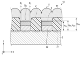
- FIG. 1 is a perspective view showing a part of an image sensor according to an embodiment of the present invention.
- FIG. 2 is a cross-sectional view of the image sensor shown in FIG. 1 taken along line II-II.
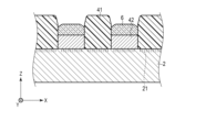
- FIG. 3 is a cross-sectional view showing one step in an example of the method for manufacturing the image sensor shown in FIGS. 1 and 2.
- FIG. 4 is a cross-sectional view showing another step in the example of the method for manufacturing the image sensor shown in FIGS. 1 and 2.
- FIG. FIG. 5 is a sectional view showing still another step in the example of the method for manufacturing the image sensor shown in FIGS. 1 and 2.
- FIG. 6 is a sectional view showing still another step in the example of the method for manufacturing the image sensor shown in FIGS. 1 and 2.
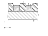
- FIG. 7 is a sectional view showing a part of an image sensor according to a modification of the embodiment of the present invention.
- FIG. 8 is a cross-sectional view showing a part of an image sensor according to a comparative example.
- FIG. 9 is a sectional view showing a part of an image sensor according to another comparative example.
- FIG. 10 is a sectional view showing a part of an image sensor according to still another comparative example.
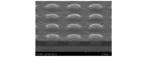
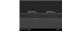
- FIG. 11 is a microscopic image taken from an oblique direction of the infrared shielding layer before heat flow in Example 1.
- FIG. 12 is a microscopic image taken from an oblique direction of the infrared shielding layer after heat flow in Example 1.
- FIG. 13 is a microscopic image of a cross section of the infrared shielding layer of FIG. 12.
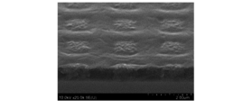
- FIG. 14 is a microscopic image taken from an oblique direction of the infrared shielding layer before heat flow in Comparative Example 1.
- FIG. 15 is a microscopic image taken from an oblique direction of the infrared shielding layer after heat flow in Comparative Example 1.
- FIG. 16 is a microscopic image of a cross section of the infrared shielding layer of FIG. 15.
- FIG. 1 is a perspective view showing a part of an image sensor according to an embodiment of the present invention.
- FIG. 2 is a cross-sectional view of the image sensor shown in FIG. 1 taken along line II-II.
- the image sensor 1A shown in FIGS. 1 and 2 is, for example, a CMOS (Complementary Metal Oxide Semiconductor) image sensor or a CCD (Charge-Coupled Device) image sensor.
- the image sensor 1A includes a substrate 2, a color filter 4 including a first colored layer 42, a second colored layer 43, and a third colored layer 44, a microlens array 5, an infrared shielding layer 6, and an infrared transmitting layer 41. Contains.
- the X direction is a direction parallel to the main surface of the substrate 2 facing the microlens array 5.
- the Y direction is parallel to the previous main surface and intersects with the X direction.
- the Z direction is a direction perpendicular to the X direction and the Y direction, that is, the thickness direction of the substrate 2.
- the substrate 2 is a semiconductor substrate such as a silicon substrate.
- a plurality of photodiodes 21, which are photoelectric conversion elements, are provided on the surface area of the substrate 2.
- the plurality of photodiodes 21 include photodiodes for each color facing each of the first colored layer 42 , the second colored layer 43 , and the third colored layer 44 , and a photodiode for infrared rays facing the infrared transmission layer 41 . .
- a photodiode for each color measures the intensity of visible light with a specific wavelength.
- An infrared photodiode measures the intensity of infrared light.
- the photodiodes 21 are arranged in the X direction and the Y direction.
- the image sensor 1A may further include a flattening layer on the main surface of the substrate 2 on the photodiode 21 side to improve adhesion.
- the color filter 4 includes a plurality of colored layers having different transmission spectra.
- the color filter 4 includes a first colored layer 42, a second colored layer 43, and a third colored layer 44.
- the number of types of colored layers included in the color filter 4 does not need to be three, as long as there are two or more types.
- the first colored layer 42, the second colored layer 43, and the third colored layer 44 have different transmission spectra.
- Each of the first colored layer 42, the second colored layer 43, and the third colored layer 44 is, for example, a red layer, a blue layer, a green layer, a yellow layer, a magenta layer, or a cyan layer.
- the first colored layer 42, the second colored layer 43, and the third colored layer 44 are a red layer, a blue layer, and a green layer.
- the first colored layer 42, the second colored layer 43, and the third colored layer 44 are a yellow colored layer, a magenta colored layer, and a cyan colored layer.
- the color filter 4 has a plurality of first through holes. As shown in FIG. 2, the first through hole is filled with an infrared transmitting layer 41.
- the first through holes and the first colored layer 42 each extend in the X direction and form a plurality of first rows arranged in the Y direction. In each of the first rows, the first through holes and the first colored layers 42 are arranged alternately in the X direction.
- the second colored layer 43 and the third colored layer 44 each extend in the X direction and form a plurality of second rows arranged in the Y direction. In each of the second rows, the second colored layers 43 and the third colored layers 44 are arranged alternately in the X direction.
- the first and second columns are arranged alternately in the Y direction.
- the first colored layer 42, the second colored layer 43, and the third colored layer 44 are each provided so as to face the photodiode for each color among the plurality of photodiodes 21, and the first through-holes is provided so as to face the infrared photodiode among the plurality of photodiodes 21.
- the color filter 4 is patterned, for example, by photolithography using a photosensitive material containing a colorant.
- each colored layer included in the color filter 4 may be different from each other or may be the same.
- the thickness of each colored layer may be, for example, in the range of 0.3 ⁇ m to 1.0 ⁇ m, or in the range of 0.4 to 0.7 ⁇ m.
- the infrared shielding layer 6 is provided on the color filter 4 and is a layer that blocks infrared rays of a specific wavelength and transmits visible light.
- the infrared shielding layer 6 blocks infrared rays in a wavelength band that can be detected as noise by each photodiode 21 facing the color filter 4. This increases the detection accuracy of these photodiodes 21.
- the infrared shielding layer 6 is provided on the color filter 4 and has a plurality of second through holes that communicate with the plurality of first through holes included in the color filter 4, respectively.
- the second through hole is filled with an infrared transmitting layer 41, as shown in FIG.
- the infrared shielding layer 6 contains, for example, an infrared absorbing coloring material and a transparent resin.
- the infrared absorbing coloring material are dyes such as squarylium dyes, croconium dyes, diimmonium dyes, anthraquinone dyes, cyanine dyes, phthalocyanine dyes, and dithiol dyes.
- the transparent resin include acrylic resin, polyamide resin, polyimide resin, polyurethane resin, polyester resin, polyether resin, polyolefin resin, polycarbonate resin, polystyrene resin, and norbornene resin.
- the infrared shielding layer 6 can be formed by a photolithography method using, for example, a photosensitive material containing an infrared absorbing coloring material, a polymerizable compound, a binder resin, a photopolymerization initiator, and the like.
- the photosensitive material may contain additives for other functions such as light stabilizers, antioxidants, heat stabilizers, and antistatic agents.
- the film thickness of the infrared shielding layer 6 may be, for example, within the range of 0.5 ⁇ m to 1.2 ⁇ m, or may be within the range of 0.7 to 1.0 ⁇ m.
- the infrared transmitting layer 41 is an optical filter that blocks visible light and transmits infrared light of a specific wavelength. That is, the infrared transmitting layer 41 transmits infrared light that can be detected by the photodiode 21 (the above-mentioned infrared photodiode) and cuts visible light that can be detected by the photodiode 21.
- the infrared transmission layer 41 increases the accuracy of infrared detection by the photodiode 21.
- the infrared rays having the specific wavelength that can be detected by the photodiode 21 are, for example, near infrared rays having a wavelength within the range of 900 nm or more and 1100 nm or less.
- the infrared transmitting layer 41 is provided on the substrate 2 in such a manner that it embeds one of the plurality of first through holes of the color filter 4 and a second through hole of the infrared shielding layer 6 that communicates with the first through hole.
- the infrared transmitting layers 41 are arranged in the X direction and the Y direction. Each of these infrared transmitting layers 41 embeds the first through hole and the second through hole communicating therewith, and protrudes upward from the upper surface of the color filter 4 .
- the infrared transmitting layer 41 contains, for example, an infrared transmitting coloring material.
- the infrared transmitting coloring material is preferably a material that transmits at least a portion of light in the near infrared region and blocks light in the visible region.
- the infrared transmitting layer 41 may contain two or more types of chromatic colorants as infrared transmitting colorants, and may exhibit black color by a combination of two or more types of chromatic colorants.
- the infrared transmitting layer 41 may contain an organic black colorant as an infrared transmitting coloring material.
- the chromatic colorant may be a pigment or a dye, but is preferably a pigment, and more preferably an organic pigment.
- the infrared transmitting layer 41 contains two or more chromatic colorants selected from, for example, a red colorant, a green colorant, a blue colorant, a yellow colorant, a purple colorant, and an orange colorant.
- the infrared transmitting layer 41 may contain inorganic oxide particles to adjust the refractive index.
- examples of the inorganic oxide include aluminum oxide, silicon oxide, zirconium oxide, and titanium oxide.
- the infrared transmitting layer 41 may contain additives for having other functions such as a light stabilizer, an antioxidant, a heat stabilizer, and an antistatic agent.
- the infrared transmitting layer 41 can be formed, for example, by a photolithography method using a photosensitive material containing an infrared transmitting coloring material, a polymerizable compound, a binder resin, a photopolymerization initiator, and the like.
- the thickness of the infrared transmitting layer 41 may be, for example, in the range of 0.9 ⁇ m to 2.3 ⁇ m, or may be in the range of 1.2 to 1.8 ⁇ m.
- the microlens array 5 is provided to face the substrate 2 with the color filter 4, the infrared shielding layer 6, and the infrared transmitting layer 41 interposed therebetween.
- the microlens array 5 is made of a colorless and transparent organic material, such as a polymer.
- the microlens array 5 includes a plurality of microlenses 51. These microlenses 51 each face the photodiode 21 with the color filter 4, infrared shielding layer 6, and infrared transmitting layer 41 interposed therebetween.
- Each of the microlenses 51 is a convex lens whose upper surface is convex.
- each microlens 51 has a circular shape when orthogonally projected onto a plane perpendicular to the Z direction. This orthographic projection may have other shapes, such as a rectangle with rounded corners.
- Each of the microlenses 51 may have a substantially hemispherical upper portion and a substantially quadrangular columnar lower portion.
- This image sensor 1A includes a plurality of pixels arranged in the X direction and the Y direction.
- each pixel includes first to fourth sub-pixels.
- the first sub-pixel includes an infrared transmitting layer 41, a photodiode 21 facing the infrared transmitting layer 41, and a microlens 51.
- the second sub-pixel includes a first colored layer 42, a photodiode 21 facing the first colored layer 42, and a microlens 51.
- the third sub-pixel includes a second colored layer 43, a photodiode 21 facing the second colored layer 43, and a microlens 51.
- the fourth sub-pixel includes a third colored layer 44, a photodiode 21 facing the third colored layer 44, and a microlens 51.
- the top surface of the infrared transmission layer 41 is located higher than the top surface of the infrared shielding layer 6.
- the upper surface of the infrared transmitting layer 41 is located at a higher position than the upper surface of the infrared shielding layer 6" means the following. That is, the upper surface of the infrared shielding layer 6 has a maximum height H CH at the boundary with the plurality of infrared transmitting layers 41, and a minimum height H CL at a position away from the boundary.
- each of the plurality of infrared transmitting layers 41 has a maximum height H PH larger than the minimum height H CL of the upper surface of the infrared shielding layer 6 (H CL ⁇ H PH ), and the infrared shielding layer 6 This means that it is greater than or equal to the maximum height H CH of the upper surface of (H CH ⁇ H PH ).
- the maximum height H CH and the minimum height H CL of the upper surface of the infrared shielding layer 6 only need to satisfy the relationship H CL ⁇ H CH .
- the image sensor 1A shown in FIG. 2 has a configuration in which the maximum height H PH of the top surface of the infrared transmitting layer 41 is higher than the maximum height H CH of the top surface of the infrared shielding layer 6, that is, the relationship H PH > H CH .
- the minimum height of the top surface of the infrared transmission layer 41 is defined as HPL
- the minimum height HPL of the top surface of the infrared transmission layer 41 is as shown in FIG.
- the upper surface of the infrared transmitting layer 41 includes a region having the maximum height HPH and a region adjacent to the region whose height reaches from the maximum height HPH to the minimum height HPL . It consists of a convex shape. Note that the above-described relationship H PH >H CL is necessarily satisfied.
- the upper surface of the infrared shielding layer 6 has a structure (H CL ⁇ H CH ).
- H CL H CH
- the upper surface of the infrared shielding layer 6 has a portion (first region D 1 ) in contact with the side surface of the infrared transmitting layer 41 that does not transmit infrared rays. It has a structure that rises toward the layer 41.
- the entire side wall of each of the plurality of second through holes included in the infrared shielding layer 6 is in contact with any side surface of the plurality of infrared transmitting layers 41. That is, in the image sensor 1A, the entire side wall of the infrared shielding layer 6 is in contact with the infrared transmitting layer 41, and there is no gap between the infrared transmitting layer 41 and the infrared shielding layer 6.
- the infrared shielding layer 6 is formed after the color filter 4 and the infrared transmitting layer 41 are formed.
- the infrared shielding layer 6 is formed by forming a pattern on the color filter 4 so that its upper surface is smaller in height than the upper surface of the infrared transmitting layer 41, and then by thermal flow.
- the upper surface of the infrared transmitting layer 41 is located at a higher position than the upper surface of the infrared shielding layer 6, the occurrence of color mixing between the infrared shielding layer 6 and the infrared transmitting layer 41 due to heat flow through the infrared shielding layer 6 is suppressed. be able to.
- the occurrence of color mixture when the upper surface of the infrared transmitting layer 41 is located at a lower position than the upper surface of the infrared shielding layer 6 will be described later using a comparative example.
- the difference HD between the height of the top surface of the infrared transmitting layer 41 and the height of the top surface of the infrared shielding layer 6 is 0 ⁇ HD , preferably 0.05 ⁇ m ⁇ HD , more preferably 0.1 ⁇ m ⁇ HD .
- the difference in height of the upper surface HD is HD ⁇ 1.0 ⁇ m, more preferably HD ⁇ 0.8 ⁇ m, and it is preferable that HD ⁇ 0.3 ⁇ m. More preferred.
- the entire side wall of the infrared shielding layer 6 can be brought into contact with the side surface of the infrared transmitting layer 41, as described above, and there is a gap between the infrared transmitting layer 41 and the infrared shielding layer 6. This makes it possible to prevent gaps from forming. This suppresses the generation of stray light and reduces noise.
- the above-mentioned effect of causing the infrared shielding layer 6 to undergo heat flow is more likely to be obtained when the infrared shielding layer 6 contains a dye as the infrared absorbing coloring material rather than a pigment.
- each of the plurality of infrared transmitting layers 41 is convex.
- a lens effect is produced for the light condensed by the microlens 51 facing the infrared transmitting layer 41, and the detection accuracy of infrared rays is improved.
- a plurality of first regions D1 are arranged with a plurality of first regions in between.
- the height is greater than that of the second region D2 adjacent to the second through hole.
- a portion of the upper surface of the infrared shielding layer 6 that contacts the side surface of the infrared transmitting layer 41 rises toward the infrared transmitting layer 41. If a valley is formed between the side surface of the infrared shielding layer 6 and the side surface of the infrared transmitting layer 41, defects such as voids (gaps) are likely to occur when the microlens array 5 is formed.
- the height of the first region D1 on the upper surface of the infrared shielding layer 6 is greater than that of the second region D2 , so the occurrence of defects such as voids is suppressed. .
- the portion of the upper surface of the infrared shielding layer 6 that is in contact with the side surface of the infrared transmitting layer 41 has a structure that rises toward the infrared transmitting layer 41. easy to cause. Therefore, the effect of suppressing voids by causing heat to flow through the infrared shielding layer 6 is improved when the infrared shielding layer 6 contains a dye instead of a pigment as an infrared absorbing coloring material.
- This image sensor 1A can be manufactured, for example, by the following method.
- 3 to 6 are cross-sectional views showing steps included in an example of the method for manufacturing the image sensor 1A shown in FIGS. 1 and 2, respectively.
- the color filter 4 is formed on the substrate 2.
- the color filter 4 includes the first colored layer 42, the second colored layer 43, and the third colored layer 44, and has a plurality of first through holes. As shown in FIG. 3, each of the first through holes T is located between adjacent first colored layers 42 in the X direction. Moreover, each of the first through holes T is located between the second colored layers 43 adjacent to each other in the Y direction.
- the first colored layer 42 is formed by forming a coating film made of a photosensitive material containing a colorant on the substrate 2, and patterning this coating film using a photography method including exposure, development, and baking. .
- the second colored layer 43 and the third colored layer 44 are also formed by the same method as the first colored layer 42.
- the first colored layer 42, the second colored layer 43, and the third colored layer 44 may be formed in any order.
- the patterning of the first colored layer 42, the second colored layer 43, and the third colored layer 44 includes a plurality of first rows in which the first through holes T and the first colored layer 42 are arranged alternately in the X direction, and A plurality of second rows in which the second colored layers 43 and the third colored layers 44 are alternately arranged in the X direction are arranged alternately in the Y direction.
- organic or inorganic pigments can be used alone or in a mixture of two or more types.
- the pigment is preferably a pigment with high color development and high heat resistance, particularly a pigment with high heat decomposition resistance, and organic pigments are usually used.
- Pigments that can be used include phthalocyanine, azo, anthraquinone, quinacridone, dioxazine, anthanthrone, indanthrone, perylene, thioindigo, isoindoline, quinophthalone, and diketopyrrolopyrrole. Examples include organic pigments such as pigments.
- an infrared transmitting layer 41 is formed on the substrate 2.
- an infrared transmitting layer 41 is formed at the position of the first through hole T shown in FIG. 3, and the infrared transmitting layer 41 and the first colored layer 42 are arranged alternately.
- the infrared transmitting layer 41 includes exposure, development, and baking using a photosensitive material containing an infrared transmitting coloring material so as to embed each of the plurality of first through holes T and protrude from the plurality of first through holes T.
- the pattern is formed by photolithography.
- an infrared shielding layer 6 is formed on the color filter 4, and heat is caused to flow through the layer.
- 5 and 6 show cross-sectional views of the process in which the infrared shielding layer 6 is formed on the first colored layer 42 included in the color filter 4.
- FIG. 5 is a cross-sectional view of the process before the infrared shielding layer 6 is subjected to heat flow
- FIG. 6 is a process cross-sectional view after the infrared shielding layer 6 is subjected to heat flow.
- the infrared shielding layer 6 is first formed using a photosensitive material containing an infrared absorbing colorant so that its upper surface has a smaller height than the upper surface of the infrared transmitting layer 41. , formed on the color filter 4.
- the infrared shielding layer 6 is formed by a photolithography method including exposure and development.
- the side surface (the side wall of the second through hole) of the infrared shielding layer 6 is the side surface of the infrared transmitting layer 41, as shown in FIG. They are not in contact with each other and form a groove-like gap with the infrared transmitting layer 41.
- the entire side surface of the infrared shielding layer 6 comes into contact with the side surface of the infrared transmitting layer 41, as shown in FIG. The groove-like gap that was formed between them disappears.
- the microlenses 51 are formed to face each of the plurality of photodiodes 21 with the color filter 4, infrared shielding layer 6, and infrared transmitting layer 6 interposed therebetween.
- Each microlens 51 is formed using, for example, an etch-back method.
- the etch-back method first, a transparent resin layer for forming each microlens 51 is formed so as to face the substrate 2 with the color filter 4, infrared shielding layer 6, and infrared transmitting layer 6 interposed therebetween.
- a resist pattern having a shape in which a plurality of hemispheres are lined up (lens shape) is formed on the transparent resin layer.
- a plurality of microlenses 51 are formed by dry etching the transparent resin layer provided with the resist pattern to transfer the shape (lens shape) of the resist pattern to the transparent resin layer.
- Examples of the transparent resin used to form the microlens 51 include acrylic resin, polyamide resin, polyimide resin, polyurethane resin, polyester resin, polyether resin, polyolefin resin, polycarbonate resin, and polystyrene resin. These include resins and norbornene-based resins.
- the microlens 51 can also be formed without an etching mask. That is, first, a coating film made of a photosensitive material is formed so as to face the substrate 2 with the color filter 4, infrared shielding layer 6, and infrared transmitting layer 6 interposed therebetween. Next, this coating film is patterned by a photolithography method that includes exposure and development, and a plurality of microlenses 51 made of a cured photosensitive material are formed into photodiodes 21 with color separation filters 4 in between. Form them so that they are facing each other. Note that this patterning preferably further includes heat flow due to heating after development. In the manner described above, the image sensor 1A shown in FIGS. 1 and 2 is obtained.
- the image sensor 1A obtained by this method has excellent detection accuracy for infrared rays. This will be explained below with reference to comparative examples.
- the infrared shielding layer 6 is formed so that the upper surface thereof is smaller than that of the infrared transmission layer 41. Form to have a small height and allow heat flow. Since the upper surface of the infrared transmitting layer 41 is located at a higher position than the upper surface of the infrared shielding layer 6, the upper surface of the infrared transmitting layer 41 is not partially covered by the infrared shielding layer 6 by causing heat to flow through the infrared shielding layer 6. , Therefore, the occurrence of color mixture caused by this can be suppressed.
- the infrared shielding layer 6 by filling the recesses after forming the infrared transmitting layer 6 and causing heat to flow through the infrared shielding layer 6, the entire side surface of the infrared shielding layer 6 is covered with the infrared transmitting layer 41, as described above. It can be brought into contact with the side surface, making it possible to suppress the generation of groove-like gaps. Since there is no groove-like gap, the generation of stray light due to the small thickness of the infrared shielding layer 6 at this position is suppressed, and noise can be reduced.
- the infrared shielding layer 6 by causing the infrared shielding layer 6 to flow through heat, it is possible not only to prevent a gap from occurring between the infrared transmitting layer 41 and the infrared shielding layer 6, but also to prevent the infrared shielding layer 6 from forming as described above. It is also possible to have a structure in which a portion of the upper surface that contacts the side surface of the infrared transmitting layer 41 rises toward the infrared transmitting layer 41. In this case, generation of voids (gaps) can be suppressed.
- FIG. 8 is a cross-sectional view showing a part of an image sensor according to a comparative example.
- the upper surface of the infrared transmitting layer 41 is located at a lower position than the upper surface of the infrared shielding layer 6, and has a concave shape.
- the image sensor 100A includes a step of forming a color filter 4 including a second colored layer 42 on a substrate 2, a step of forming an infrared shielding layer 6 on the color filter 4, and a step of forming an infrared transmitting layer 41. It was manufactured by a method including this order. In this process order, the infrared transmitting layer 41 fills the first and second through holes of the color filter 4 and the infrared shielding layer 6, respectively, and its upper surface is higher than the upper surface of the infrared shielding layer 6. It is spin-coated onto the substrate 2 so as to be small and formed by photolithography. In this case, the upper surface of the infrared transmitting layer 41 tends to have a concave shape as shown in FIG.
- the upper surface of the infrared transmitting layer 41 has a concave shape as in the image sensor 100A, the light condensing effect by the microlens 51 facing it is reduced, and the detection accuracy of infrared rays is reduced.
- FIG. 9 and 10 are cross-sectional views showing a part of an image sensor according to another comparative example, respectively.
- the image sensor 100B shown in FIG. 9 and the image sensor 100C shown in FIG. It is shaped like this.
- the image sensors 100B and 100C are manufactured by changing the order of the step of forming the infrared shielding layer 6 and the step of forming the infrared transmitting layer 41 with respect to the above manufacturing method of the image sensor 100A. That is, the image sensors 100B and 100C are manufactured by a method that includes the steps of forming the color filter 4 including the first colored layer 42, forming the infrared transmitting layer 41, and forming the infrared shielding layer 6 in this order. It is what was done.
- the infrared shielding layer 6 is formed by coating a photosensitive material containing an infrared absorbing coloring material on the upper surface of the infrared transmitting layer 41 and the upper surface of the color filter 4, and coloring it by a photolithography method including exposure, development, and baking. A pattern is formed on the filter 4.
- the above-mentioned dye-based pigment is often used as an infrared absorbing coloring material.
- photosensitive materials containing dye-based pigments tend to have side surfaces tapered due to thermal flow during firing.
- the side surface of the infrared shielding layer 6 is tapered and covers a part of the upper surface adjacent to the side surface of the infrared transmitting layer 41, color mixing is likely to occur. Furthermore, in the image sensor 100C shown in FIG. 10, since the tapered side surface of the infrared shielding layer 6 exists within the pixel including the first colored layer 42, stray light is likely to occur.
- FIG. 7 is a sectional view showing a part of an image sensor according to a modification of the image sensor 1A.
- the image sensor 1B shown in FIG. 7 is the same as the image sensor 1A shown in FIGS. 1 and 2, except that the first colored layer 42 has an inversely tapered cross-sectional shape. Since the first colored layer 42 has an inverted tapered cross-sectional shape, the infrared transmitting layer 41 becomes difficult to fall off due to the anchor effect.
- a colored layer having an inverted tapered cross-sectional shape can be obtained by appropriately combining known techniques, such as adding an appropriate amount of an additive such as an ultraviolet absorber to the photosensitive material forming the colored layer. .
- Example 1 A part of the structure included in the image sensor 1A shown in FIG. 6 (hereinafter referred to as "partial structure” or “partial structure of image sensor”) was manufactured by the method shown below.
- - First step First three types of photosensitive materials containing different pigments were prepared. Using these materials, a first colored layer 42, a second colored layer 43, and a third colored layer 44 were patterned on the substrate 2 by a photolithography method including exposure, development, and baking to form a color filter 4 (Fig. 3 reference).
- the first colored layer 42, the second colored layer 43, and the third colored layer 44 were a red layer, a green layer, and a blue layer, respectively.
- the thickness of each of these colored layers was 0.5 ⁇ m.
- an infrared transmitting coloring material a polymerizable compound, a binder resin, and a photopolymerization initiator are contained on the color filter 4 and in a portion of the upper surface of the substrate 2 that is not covered by the color filter 4.
- a coating film was formed by applying a photosensitive material.
- the infrared transmitting coloring material a mixed coloring material of a red organic pigment, a green organic pigment, and a blue organic pigment was used.
- the coating film was patterned by a photolithography method including exposure, development, and baking to form an infrared transmitting layer 41 that filled the first through hole T and protruded from the first through hole T (see FIG. 4).
- the thickness of the obtained infrared transmitting layer 41 was 1.5 ⁇ m.
- the film thickness of the infrared transmitting layer 41 means the maximum height HPH shown in FIG.
- a photosensitive material containing an infrared absorbing coloring material, a polymerizable compound, an acrylic resin, a photopolymerization initiator, etc. is made so that its upper surface has a smaller height than the infrared transmitting layer 41.
- a coating film was formed by coating it on the color filter 4 so as to have the following properties.
- squarylium dye was used as the infrared absorbing coloring material.
- the coating film was patterned by a photolithography method including exposure and development to form an infrared shielding layer 6 (see FIG. 5).
- FIG. 11 is an electron micrograph taken from an oblique direction of the partial structure provided with the infrared shielding layer 6 after exposure and development and before heat flow obtained in the third step.
- the infrared shielding layer 6 obtained in the third step was fired to cause heat flow.
- a partial structure of the image sensor 1A was manufactured by omitting the microlens array 5 from the image sensor 1A.
- the film thickness of the infrared shielding layer 6 means the film thickness obtained by subtracting the film thickness of the color filter 4 from the minimum height HCL shown in FIG.
- FIG. 12 is an electron micrograph taken from an oblique direction of the partial structure provided with the infrared shielding layer 6 after heat flow obtained in the fourth step
- FIG. 13 is an electron microscope photograph taken of a cross section of the partial structure. It is. From comparison with FIG. 11, it was confirmed that the gap between the infrared shielding layer 6 and the infrared transmitting layer 41 was eliminated due to the heat flow in the infrared shielding layer 6. On the other hand, since the upper surface of the infrared transmitting layer 41 was higher than the upper surface of the infrared shielding layer 6, it was confirmed that the upper surface of the infrared shielding layer 6 was not covered by the infrared shielding layer 6 subjected to heat flow. Therefore, it can be seen that in the image sensor 1A obtained by the manufacturing method of Example 1, color mixture and generation of stray light are suppressed.
- Color filter 4 was formed on the substrate 2 by the same method as the first step of Example 1 (see FIG. 3). The thickness of each colored layer was 0.5 ⁇ m.
- Example 2 the same as the second step of Example 1 except that the amount of photosensitive material applied to the color filter 4 and the portion of the upper surface of the substrate 2 that is not covered by the color filter 4 was changed.
- An infrared transmitting layer 41 was formed by the method (see FIG. 4). The thickness of the obtained infrared transmitting layer 41 was 1.0 ⁇ m.
- FIG. 14 is an electron micrograph taken from an oblique direction of a partial structure of an image sensor according to a comparative example including the infrared shielding layer 6 after exposure and development and before heat flow obtained in the third step.
- the infrared shielding layer 6 obtained in the third step was fired to cause heat flow.
- a partial structure of an image sensor was manufactured by omitting the microlens array 5 from the image sensor 100B shown in FIG.
- FIG. 15 is an electron micrograph taken from an oblique direction of the partial structure of the image sensor equipped with the infrared shielding layer 6 after heat flow obtained in the fourth step
- FIG. 16 is an image taken of a cross section of the partial structure. This is an electron micrograph. From comparison with FIG. 14, it was confirmed that the upper surface peripheral portion of the infrared transmitting layer 41 was covered with the infrared shielding layer 6 due to the heat flow of the infrared shielding layer 6. It is presumed that color mixing is likely to occur in image sensors manufactured using this.
- the present invention is not limited to the above-described embodiments, and can be variously modified at the implementation stage without departing from the gist thereof.
- each embodiment may be implemented in combination as appropriate, and in that case, the combined effect can be obtained.
- the embodiments described above include various inventions, and various inventions can be extracted by combinations selected from the plurality of constituent features disclosed. For example, if a problem can be solved and an effect can be obtained even if some constituent features are deleted from all the constituent features shown in the embodiment, the configuration from which these constituent features are deleted can be extracted as an invention.
Abstract
Provided is a technology that makes it possible to improve the detection accuracy of an image sensor with respect to infrared radiation. An image sensor 1A comprises: a substrate 2 on which a plurality of photodiodes are provided; a color filter 4 which includes a plurality of coloration layers and has a plurality of first through-holes; an infrared radiation blocking layer 6 which is provided on the color filter and has a plurality of second through-holes respectively communicating with the plurality of first through-holes; a plurality of infrared radiation transmissive layers 41 in each of which one of the plurality of first through-holes and the second through-hole communicating therewith are embedded; and a plurality of micro lenses 51. In the image sensor 1A, the side wall of each of the plurality of second through-holes is entirely in contact with the side surface of any of the plurality of infrared radiation transmissive layers 41. The upper surface of the infrared radiation blocking layer has a maximum height HCH at the position of the boundary thereof with the plurality of infrared radiation transmissive layers 41, and has a minimum height HCL at a position away from the boundary. The upper surface of each of the plurality of infrared radiation transmissive layers 41 has a maximum height HPH that is greater than the minimum height HCL and is greater than or equal to the maximum height HCH.
Description
本発明は、イメージセンサ及びその製造方法に関する。
The present invention relates to an image sensor and a manufacturing method thereof.
イメージセンサ(又は固体撮像素子)は、光をその強度に対応した大きさの電気信号に変換する複数のフォトダイオードが形成された基板を備えている。イメージセンサとしては、各色用のフォトダイオード上に位置するカラーフィルタと、赤外線用のフォトダイオード上に位置する赤外線透過層と、上記カラーフィルタ上に設けられた赤外線遮蔽層とを備えたものがある(例えば、特許文献1を参照)。
An image sensor (or solid-state image sensor) includes a substrate on which a plurality of photodiodes are formed that convert light into an electrical signal of a size corresponding to the intensity of the light. Some image sensors include a color filter located on a photodiode for each color, an infrared transmission layer located on an infrared photodiode, and an infrared shielding layer provided on the color filter. (For example, see Patent Document 1).
特許文献1に記載のイメージセンサは、赤外線透過層の上面が赤外線遮蔽層の上面より低い構造を有している。同文献では、基板上の各色用フォトダイオードの上にカラーフィルタを形成し、その上層として赤外線遮蔽層を形成した後で、基板上の赤外線用フォトダイオードの位置に存在する凹部を穴埋めする形で赤外線透過層を形成することで、上記構造を有するイメージセンサを製造している。
The image sensor described in Patent Document 1 has a structure in which the top surface of the infrared transmission layer is lower than the top surface of the infrared shielding layer. In this document, a color filter is formed on the photodiode for each color on the substrate, an infrared shielding layer is formed as an upper layer, and then the recesses existing at the positions of the infrared photodiodes on the substrate are filled. An image sensor having the above structure is manufactured by forming an infrared transmitting layer.
本発明は、イメージセンサの赤外線に対する検出精度を向上させることができる技術を提供することを目的とする。
An object of the present invention is to provide a technique that can improve the detection accuracy of an image sensor for infrared rays.
本発明の一側面によると、
複数のフォトダイオードが設けられた基板と、
上記複数のフォトダイオードの一部の上にそれぞれ設けられた複数の着色層を含み、上記複数のフォトダイオードの他の一部の位置にそれぞれ設けられた複数の第1貫通孔を有するカラーフィルタと、
上記カラーフィルタの上に設けられ、特定波長の赤外線を遮り、可視光を透過させる赤外線遮蔽層であって、上記複数の第1貫通孔とそれぞれ連通した複数の第2貫通孔を有する赤外線遮蔽層と、
上記複数の第1貫通孔の1つ及びこれと連通した上記第2貫通孔を各々が埋め込み、可視光を遮り、上記特定波長の赤外線を透過させる複数の赤外線透過層と、
上記カラーフィルタと上記赤外線遮蔽層と上記複数の赤外線透過層とを間に挟んで上記複数のフォトダイオードとそれぞれ向き合った複数のマイクロレンズと
を備え、
上記複数の第2貫通孔の各々の側壁は、その全体が上記複数の赤外線透過層の何れかの側面と接触し、
上記赤外線遮蔽層の上面は、上記複数の赤外線透過層との境界の位置に最大高さHCHを有するとともに、上記境界から離れた位置に最小高さHCLを有し、
上記複数の赤外線透過層の各々の上面は、最大高さHPHが上記最小高さHCLと比較してより大きく、上記最大高さHCH以上であるイメージセンサが提供される。 According to one aspect of the invention:
A substrate provided with a plurality of photodiodes,
A color filter including a plurality of colored layers each provided on a part of the plurality of photodiodes, and having a plurality of first through holes each provided at a position of another part of the plurality of photodiodes; ,
An infrared shielding layer provided on the color filter to block infrared rays of a specific wavelength and transmit visible light, the infrared shielding layer having a plurality of second through holes each communicating with the plurality of first through holes. and,
a plurality of infrared transmitting layers each embedding one of the plurality of first through holes and the second through hole communicating therewith, blocking visible light and transmitting infrared rays of the specific wavelength;
a plurality of microlenses each facing the plurality of photodiodes with the color filter, the infrared shielding layer, and the plurality of infrared transmission layers sandwiched therebetween;
The entire side wall of each of the plurality of second through holes is in contact with any side surface of the plurality of infrared transmitting layers,
The upper surface of the infrared shielding layer has a maximum height HCH at a boundary with the plurality of infrared transmitting layers, and a minimum height HCL at a position away from the boundary,
An image sensor is provided in which a top surface of each of the plurality of infrared transmitting layers has a maximum height H PH greater than the minimum height H CL and greater than or equal to the maximum height H CH .
本発明の他の側面によると、上記複数の赤外線透過層の各々の上記上面は凸状である上記側面に係るイメージセンサが提供される。
According to another aspect of the present invention, there is provided an image sensor according to the side surface, wherein the upper surface of each of the plurality of infrared transmitting layers is convex.
本発明の更に他の側面によると、上記赤外線遮蔽層の上記上面のうち、上記複数の第2貫通孔に各々が隣接した複数の第1領域は、上記複数の第1領域を間に挟んで上記複数の第2貫通孔と各々が隣り合った第2領域と比較して高さがより大きい上記側面の何れかに係るイメージセンサが提供される。
According to still another aspect of the present invention, on the upper surface of the infrared shielding layer, the plurality of first regions each adjacent to the plurality of second through holes are arranged with the plurality of first regions in between. There is provided an image sensor according to any one of the above-mentioned side surfaces, each of which is larger in height than the second region adjacent to the plurality of second through-holes.
本発明の更に他の側面によると、上記複数の着色層のうち上記複数の赤外線透過層と接しているものの1以上は、逆テーパー状の断面形状を有している上記属面の何れかに係るイメージセンサが提供される。
According to still another aspect of the present invention, one or more of the plurality of colored layers that are in contact with the plurality of infrared transmitting layers has an inverted tapered cross-sectional shape. Such an image sensor is provided.
本発明の更に他の側面によると、
複数の着色層を含み、複数の貫通孔を有するカラーフィルタを、基板に設けられた複数のフォトダイオードの一部の上に上記複数の着色層がそれぞれ設けられ、上記複数のフォトダイオードの他の一部の位置に上記複数の貫通孔が設けられるように形成することと、 可視光を遮り、特定波長の赤外線を透過させる複数の赤外線透過層を、上記複数の貫通孔をそれぞれ埋め込み且つ上記複数の貫通孔から突き出るように形成することと、
上記特定波長の赤外線を遮り、可視光を透過させる赤外線遮蔽層を、上記赤外線遮蔽層の上面が上記複数の赤外線透過層と比較してより小さな高さを有するように、上記カラーフィルタの上に形成することと、
上記赤外線遮蔽層を熱フローさせることと、
その後、複数のマイクロレンズを、上記カラーフィルタと上記赤外線遮蔽層と上記複数の赤外線透過層とを間に挟んで上記複数のフォトダイオードとそれぞれ向き合うように形成することと
を含んだイメージセンサの製造方法が提供される。 According to yet another aspect of the invention,
A color filter including a plurality of colored layers and having a plurality of through holes is provided, wherein each of the plurality of colored layers is provided on a part of a plurality of photodiodes provided on a substrate, and the other of the plurality of photodiodes is provided on a substrate. The plurality of through holes are formed at some positions, and the plurality of infrared transmitting layers that block visible light and transmit infrared rays of a specific wavelength are embedded in each of the plurality of through holes and the plurality of through holes are respectively embedded. formed so as to protrude from the through hole of the
An infrared shielding layer that blocks infrared rays of the specific wavelength and transmits visible light is placed on the color filter such that the upper surface of the infrared shielding layer has a smaller height than the plurality of infrared transmitting layers. to form and
causing heat to flow through the infrared shielding layer;
After that, manufacturing an image sensor including forming a plurality of microlenses so as to face each of the plurality of photodiodes with the color filter, the infrared shielding layer, and the plurality of infrared transmission layers interposed therebetween. A method is provided.
本発明によれば、イメージセンサの赤外線に対する検出精度を向上させることができる技術が提供される。
According to the present invention, a technique is provided that can improve the detection accuracy of an image sensor for infrared rays.
以下に、本発明の実施形態について、図面を参照しながら説明する。以下に説明する実施形態は、上記側面の何れかをより具体化したものである。以下に記載する事項は、単独で又は複数を組み合わせて、上記側面の各々に組み入れることができる。
Embodiments of the present invention will be described below with reference to the drawings. The embodiments described below are more specific implementations of any of the above aspects. The matters described below can be incorporated into each of the above aspects singly or in combination.
また、以下に示す実施形態は、本発明の技術的思想を具体化するための構成を例示するものであって、本発明の技術的思想は、下記の構成部材の材質、形状、及び構造等によって限定されるものではない。本発明の技術的思想には、請求の範囲に記載された請求項が規定する技術的範囲内において、種々の変更を加えることができる。
In addition, the embodiments shown below illustrate configurations for embodying the technical idea of the present invention, and the technical idea of the present invention includes the materials, shapes, structures, etc. of the following constituent members. It is not limited by. Various changes can be made to the technical idea of the present invention within the technical scope defined by the claims.
なお、同様又は類似した機能を有する要素については、以下で参照する図面において同一の参照符号を付し、重複する説明は省略する。また、図面は模式的なものであり、或る方向の寸法と別の方向の寸法との関係、及び、或る部材の寸法と他の部材の寸法との関係等は、現実のものとは異なり得る。
Note that elements having the same or similar functions are designated by the same reference numerals in the drawings referred to below, and duplicate explanations will be omitted. In addition, the drawings are schematic, and the relationship between dimensions in one direction and dimensions in another direction, and the relationship between the dimensions of a certain member and the dimensions of other members, etc. may differ from the actual one. It can be different.
図1は、本発明の一実施形態に係るイメージセンサの一部を示す斜視図である。図2は、図1に示すイメージセンサのII-II線に沿った断面図である。
FIG. 1 is a perspective view showing a part of an image sensor according to an embodiment of the present invention. FIG. 2 is a cross-sectional view of the image sensor shown in FIG. 1 taken along line II-II.
図1及び図2に示すイメージセンサ1Aは、例えば、CMOS(Complementary Metal Oxide Semiconductor)イメージセンサ又はCCD(Charge-Coupled Device)イメージセンサである。イメージセンサ1Aは、基板2と、第1着色層42、第2着色層43及び第3着色層44を含むカラーフィルタ4と、マイクロレンズアレイ5と、赤外線遮蔽層6と、赤外線透過層41とを含んでいる。
The image sensor 1A shown in FIGS. 1 and 2 is, for example, a CMOS (Complementary Metal Oxide Semiconductor) image sensor or a CCD (Charge-Coupled Device) image sensor. The image sensor 1A includes a substrate 2, a color filter 4 including a first colored layer 42, a second colored layer 43, and a third colored layer 44, a microlens array 5, an infrared shielding layer 6, and an infrared transmitting layer 41. Contains.
なお、各図において、X方向は、基板2のマイクロレンズアレイ5と向き合った主面に平行な方向である。Y方向は、先の主面に平行であり且つX方向と交差する方向である。Z方向は、X方向及びY方向に対して垂直な方向、即ち、基板2の厚さ方向である。ここでは、一例として、X方向及びY方向は、互いに対して垂直であるとする。
Note that in each figure, the X direction is a direction parallel to the main surface of the substrate 2 facing the microlens array 5. The Y direction is parallel to the previous main surface and intersects with the X direction. The Z direction is a direction perpendicular to the X direction and the Y direction, that is, the thickness direction of the substrate 2. Here, as an example, it is assumed that the X direction and the Y direction are perpendicular to each other.
<基板>
基板2は、シリコン基板等の半導体基板である。基板2の表面領域には、図2に示すように、光電変換素子である複数のフォトダイオード21が設けられている。複数のフォトダイオード21は、第1着色層42、第2着色層43及び第3着色層44の各々に向き合った各色用のフォトダイオードと、赤外線透過層41に向き合った赤外線用のフォトダイオードを含む。各色用のフォトダイオードは、特定の波長を有する可視光の強度を測定する。赤外線用のフォトダイオードは、赤外線の強度を測定する。フォトダイオード21は、X方向とY方向とに配列している。 <Substrate>
Thesubstrate 2 is a semiconductor substrate such as a silicon substrate. As shown in FIG. 2, a plurality of photodiodes 21, which are photoelectric conversion elements, are provided on the surface area of the substrate 2. The plurality of photodiodes 21 include photodiodes for each color facing each of the first colored layer 42 , the second colored layer 43 , and the third colored layer 44 , and a photodiode for infrared rays facing the infrared transmission layer 41 . . A photodiode for each color measures the intensity of visible light with a specific wavelength. An infrared photodiode measures the intensity of infrared light. The photodiodes 21 are arranged in the X direction and the Y direction.
基板2は、シリコン基板等の半導体基板である。基板2の表面領域には、図2に示すように、光電変換素子である複数のフォトダイオード21が設けられている。複数のフォトダイオード21は、第1着色層42、第2着色層43及び第3着色層44の各々に向き合った各色用のフォトダイオードと、赤外線透過層41に向き合った赤外線用のフォトダイオードを含む。各色用のフォトダイオードは、特定の波長を有する可視光の強度を測定する。赤外線用のフォトダイオードは、赤外線の強度を測定する。フォトダイオード21は、X方向とY方向とに配列している。 <Substrate>
The
イメージセンサ1Aは、基板2のフォトダイオード21側の主面上に、密着性の向上のために平坦化層を更に含んでいてもよい。
The image sensor 1A may further include a flattening layer on the main surface of the substrate 2 on the photodiode 21 side to improve adhesion.
<カラーフィルタ>
カラーフィルタ4は、透過スペクトルが異なる複数の着色層を含んでいる。ここでは、カラーフィルタ4は、第1着色層42、第2着色層43及び第3着色層44を含んでいる。カラーフィルタ4が含む着色層の種類は、2種以上であれば、3種でなくてもよい。 <Color filter>
The color filter 4 includes a plurality of colored layers having different transmission spectra. Here, the color filter 4 includes a firstcolored layer 42, a second colored layer 43, and a third colored layer 44. The number of types of colored layers included in the color filter 4 does not need to be three, as long as there are two or more types.
カラーフィルタ4は、透過スペクトルが異なる複数の着色層を含んでいる。ここでは、カラーフィルタ4は、第1着色層42、第2着色層43及び第3着色層44を含んでいる。カラーフィルタ4が含む着色層の種類は、2種以上であれば、3種でなくてもよい。 <Color filter>
The color filter 4 includes a plurality of colored layers having different transmission spectra. Here, the color filter 4 includes a first
第1着色層42、第2着色層43及び第3着色層44は、透過スペクトルが異なっている。第1着色層42、第2着色層43及び第3着色層44の各々は、例えば、赤色層、青色層、緑色層、イエロー色層、マゼンタ色層、又はシアン色層である。一例によれば、第1着色層42、第2着色層43及び第3着色層44は、赤色層、青色層及び緑色層である。他の例によれば、第1着色層42、第2着色層43及び第3着色層44は、イエロー色層、マゼンタ色層及びシアン色層である。
The first colored layer 42, the second colored layer 43, and the third colored layer 44 have different transmission spectra. Each of the first colored layer 42, the second colored layer 43, and the third colored layer 44 is, for example, a red layer, a blue layer, a green layer, a yellow layer, a magenta layer, or a cyan layer. According to one example, the first colored layer 42, the second colored layer 43, and the third colored layer 44 are a red layer, a blue layer, and a green layer. According to another example, the first colored layer 42, the second colored layer 43, and the third colored layer 44 are a yellow colored layer, a magenta colored layer, and a cyan colored layer.
カラーフィルタ4は、複数の第1貫通孔を有している。図2に示すように、第1貫通孔は、赤外線透過層41によって埋め込まれている。
The color filter 4 has a plurality of first through holes. As shown in FIG. 2, the first through hole is filled with an infrared transmitting layer 41.
カラーフィルタ4において、第1貫通孔と第1着色層42は、X方向へ各々が伸び、Y方向へ配列した複数の第1列を形成している。第1列の各々において、第1貫通孔及び第1着色層42は、X方向へ交互に配列している。第2着色層43及び第3着色層44は、X方向へ各々が伸び、Y方向へ配列した複数の第2列を形成している。第2列の各々において、第2着色層43及び第3着色層44は、X方向へ交互に配列している。そして、第1列及び第2列は、Y方向へ交互に配列している。
In the color filter 4, the first through holes and the first colored layer 42 each extend in the X direction and form a plurality of first rows arranged in the Y direction. In each of the first rows, the first through holes and the first colored layers 42 are arranged alternately in the X direction. The second colored layer 43 and the third colored layer 44 each extend in the X direction and form a plurality of second rows arranged in the Y direction. In each of the second rows, the second colored layers 43 and the third colored layers 44 are arranged alternately in the X direction. The first and second columns are arranged alternately in the Y direction.
上記の通り、第1着色層42、第2着色層43及び第3着色層44は、複数のフォトダイオード21の中の各色用のフォトダイオードと向き合うようにそれぞれ設けられ、複数の第1貫通孔は、複数のフォトダイオード21の中の赤外線用のフォトダイオードと向き合うように設けられている。
As described above, the first colored layer 42, the second colored layer 43, and the third colored layer 44 are each provided so as to face the photodiode for each color among the plurality of photodiodes 21, and the first through-holes is provided so as to face the infrared photodiode among the plurality of photodiodes 21.
カラーフィルタ4は、例えば、着色剤を含む感光性材料を用いて、フォトリソグラフィ法によりパターン形成される。
The color filter 4 is patterned, for example, by photolithography using a photosensitive material containing a colorant.
カラーフィルタ4に含まれる各着色層の膜厚は、互いに異なっていてもよいし、同じであってもよい。各着色層の膜厚は、例えば、0.3μm乃至1.0μmの範囲内であってよく、0.4乃至0.7μmの範囲内であってよい。
The thickness of each colored layer included in the color filter 4 may be different from each other or may be the same. The thickness of each colored layer may be, for example, in the range of 0.3 μm to 1.0 μm, or in the range of 0.4 to 0.7 μm.
<赤外線遮蔽層>
赤外線遮蔽層6は、カラーフィルタ4の上に設けられ、特定波長の赤外線を遮り、可視光を透過させる層である。赤外線遮蔽層6は、カラーフィルタ4と向き合った各フォトダイオード21がノイズとして検出し得る波長帯の赤外線をカットする。それによって、これらフォトダイオード21の検出精度を高める。 <Infrared shielding layer>
Theinfrared shielding layer 6 is provided on the color filter 4 and is a layer that blocks infrared rays of a specific wavelength and transmits visible light. The infrared shielding layer 6 blocks infrared rays in a wavelength band that can be detected as noise by each photodiode 21 facing the color filter 4. This increases the detection accuracy of these photodiodes 21.
赤外線遮蔽層6は、カラーフィルタ4の上に設けられ、特定波長の赤外線を遮り、可視光を透過させる層である。赤外線遮蔽層6は、カラーフィルタ4と向き合った各フォトダイオード21がノイズとして検出し得る波長帯の赤外線をカットする。それによって、これらフォトダイオード21の検出精度を高める。 <Infrared shielding layer>
The
赤外線遮蔽層6は、カラーフィルタ4の上に設けられ、カラーフィルタ4が含む複数の第1貫通孔とそれぞれ連通した複数の第2貫通孔を有する。第2貫通孔は、図2に示すように、赤外線透過層41によって埋め込まれている。
The infrared shielding layer 6 is provided on the color filter 4 and has a plurality of second through holes that communicate with the plurality of first through holes included in the color filter 4, respectively. The second through hole is filled with an infrared transmitting layer 41, as shown in FIG.
赤外線遮蔽層6は、例えば、赤外線吸収色材と透明樹脂を含有する。赤外線吸収色材は、例えば、スクアリリウム系色素、クロコニウム系色素、ジインモニウム系色素、アントラキノン系色素、シアニン系色素、フタロシアニン系色素、ジチオール系色素等の染料である。透明樹脂は、例えば、アクリル系樹脂、ポリアミド系樹脂、ポリイミド系樹脂、ポリウレタン系樹脂、ポリエステル系樹脂、ポリエーテル系樹脂、ポリオレフィン系樹脂、ポリカーボネート系樹脂、ポリスチレン系樹脂、ノルボルネン系樹脂等である。
The infrared shielding layer 6 contains, for example, an infrared absorbing coloring material and a transparent resin. Examples of the infrared absorbing coloring material are dyes such as squarylium dyes, croconium dyes, diimmonium dyes, anthraquinone dyes, cyanine dyes, phthalocyanine dyes, and dithiol dyes. Examples of the transparent resin include acrylic resin, polyamide resin, polyimide resin, polyurethane resin, polyester resin, polyether resin, polyolefin resin, polycarbonate resin, polystyrene resin, and norbornene resin.
赤外線遮蔽層6は、例えば、赤外線吸収色材、重合性化合物、バインダー樹脂、光重合開始剤等を含有する感光性材料を用いてフォトリソグラフィ法により形成することができる。感光性材料は、光安定剤、酸化防止剤、熱安定剤、帯電防止剤など、他の機能を兼ね備えるための添加物を含有してよい。
The infrared shielding layer 6 can be formed by a photolithography method using, for example, a photosensitive material containing an infrared absorbing coloring material, a polymerizable compound, a binder resin, a photopolymerization initiator, and the like. The photosensitive material may contain additives for other functions such as light stabilizers, antioxidants, heat stabilizers, and antistatic agents.
赤外線遮蔽層6の膜厚は、例えば、0.5μm乃至1.2μmの範囲内であってよく、0.7乃至1.0μmの範囲内であってよい。
The film thickness of the infrared shielding layer 6 may be, for example, within the range of 0.5 μm to 1.2 μm, or may be within the range of 0.7 to 1.0 μm.
<赤外線透過層>
赤外線透過層41は、可視光を遮り、特定波長の赤外線を透過させる光学フィルタである。すなわち、赤外線透過層41は、フォトダイオード21(上記赤外線用フォトダイオード)が検出し得る赤外線を透過させるとともに、フォトダイオード21が検出し得る可視光をカットする。赤外線透過層41により、フォトダイオード21による赤外線の検出精度が高められる。フォトダイオード21が検出し得る上記特定波長の赤外線は、例えば、900nm以上1100nm以下の範囲内の波長を有した近赤外線である。 <Infrared transmission layer>
Theinfrared transmitting layer 41 is an optical filter that blocks visible light and transmits infrared light of a specific wavelength. That is, the infrared transmitting layer 41 transmits infrared light that can be detected by the photodiode 21 (the above-mentioned infrared photodiode) and cuts visible light that can be detected by the photodiode 21. The infrared transmission layer 41 increases the accuracy of infrared detection by the photodiode 21. The infrared rays having the specific wavelength that can be detected by the photodiode 21 are, for example, near infrared rays having a wavelength within the range of 900 nm or more and 1100 nm or less.
赤外線透過層41は、可視光を遮り、特定波長の赤外線を透過させる光学フィルタである。すなわち、赤外線透過層41は、フォトダイオード21(上記赤外線用フォトダイオード)が検出し得る赤外線を透過させるとともに、フォトダイオード21が検出し得る可視光をカットする。赤外線透過層41により、フォトダイオード21による赤外線の検出精度が高められる。フォトダイオード21が検出し得る上記特定波長の赤外線は、例えば、900nm以上1100nm以下の範囲内の波長を有した近赤外線である。 <Infrared transmission layer>
The
赤外線透過層41は、カラーフィルタ4が有する複数の第1貫通孔の1つ及びこれと連通した赤外線遮蔽層6が有する第2貫通孔を各々が埋め込む形で基板2の上に設けられている。ここでは、赤外線透過層41は、X方向及びY方向へ配列している。これら赤外線透過層41の各々は、第1貫通孔及びこれに連通した第2貫通孔を埋め込むとともに、カラーフィルタ4の上面から上方へ突き出ている。
The infrared transmitting layer 41 is provided on the substrate 2 in such a manner that it embeds one of the plurality of first through holes of the color filter 4 and a second through hole of the infrared shielding layer 6 that communicates with the first through hole. . Here, the infrared transmitting layers 41 are arranged in the X direction and the Y direction. Each of these infrared transmitting layers 41 embeds the first through hole and the second through hole communicating therewith, and protrudes upward from the upper surface of the color filter 4 .
赤外線透過層41は、例えば、赤外線透過色材を含有する。赤外線透過色材は、特に近赤外領域の光の少なくとも一部を透過させ、かつ、可視領域の光を遮る材料であることが好ましい。赤外線透過層41は、赤外線透過色材として、2種類以上の有彩色着色剤を含み、2種以上の有彩色着色剤の組み合わせで黒色を呈するものであってもよい。あるいは、赤外線透過層41は、赤外線透過色材として有機系黒色着色剤を含むものであってもよい。
The infrared transmitting layer 41 contains, for example, an infrared transmitting coloring material. In particular, the infrared transmitting coloring material is preferably a material that transmits at least a portion of light in the near infrared region and blocks light in the visible region. The infrared transmitting layer 41 may contain two or more types of chromatic colorants as infrared transmitting colorants, and may exhibit black color by a combination of two or more types of chromatic colorants. Alternatively, the infrared transmitting layer 41 may contain an organic black colorant as an infrared transmitting coloring material.
有彩色着色剤は、顔料であってもよく、染料であってもよいが、好ましくは顔料であり、より好ましくは有機顔料である。赤外線透過層41は、例えば、赤色着色剤、緑色着色剤、青色着色剤、黄色着色剤、紫色着色剤およびオレンジ色着色剤から選ばれる2種以上の有彩色着色材を含有する。
The chromatic colorant may be a pigment or a dye, but is preferably a pigment, and more preferably an organic pigment. The infrared transmitting layer 41 contains two or more chromatic colorants selected from, for example, a red colorant, a green colorant, a blue colorant, a yellow colorant, a purple colorant, and an orange colorant.
赤外線透過層41は、屈折率を調整するための無機酸化物粒子を含有してよい。無機酸化物は、例えば、酸化アルミニウム、酸化珪素、酸化ジルコニウム、酸化チタン等である。また、赤外線透過層41は、光安定剤、酸化防止剤、熱安定剤、帯電防止剤など、他の機能を兼ね備えるための添加物を含有してよい。
The infrared transmitting layer 41 may contain inorganic oxide particles to adjust the refractive index. Examples of the inorganic oxide include aluminum oxide, silicon oxide, zirconium oxide, and titanium oxide. Further, the infrared transmitting layer 41 may contain additives for having other functions such as a light stabilizer, an antioxidant, a heat stabilizer, and an antistatic agent.
赤外線透過層41は、例えば、赤外線透過色材、重合性化合物、バインダー樹脂、光重合開始剤等を含有する感光性材料を用いてフォトリソグラフィ法により形成することができる。
The infrared transmitting layer 41 can be formed, for example, by a photolithography method using a photosensitive material containing an infrared transmitting coloring material, a polymerizable compound, a binder resin, a photopolymerization initiator, and the like.
赤外線透過層41の膜厚は、例えば、0.9μm乃至2.3μmの範囲内であってよく、1.2乃至1.8μmの範囲内であってよい。
The thickness of the infrared transmitting layer 41 may be, for example, in the range of 0.9 μm to 2.3 μm, or may be in the range of 1.2 to 1.8 μm.
<マイクロレンズアレイ>
マイクロレンズアレイ5は、カラーフィルタ4と赤外線遮蔽層6と赤外線透過層41とを間に挟んで、基板2と向き合うように設けられている。マイクロレンズアレイ5は、無色透明な有機物、例えば、ポリマーからなる。 <Microlens array>
Themicrolens array 5 is provided to face the substrate 2 with the color filter 4, the infrared shielding layer 6, and the infrared transmitting layer 41 interposed therebetween. The microlens array 5 is made of a colorless and transparent organic material, such as a polymer.
マイクロレンズアレイ5は、カラーフィルタ4と赤外線遮蔽層6と赤外線透過層41とを間に挟んで、基板2と向き合うように設けられている。マイクロレンズアレイ5は、無色透明な有機物、例えば、ポリマーからなる。 <Microlens array>
The
マイクロレンズアレイ5は、複数のマイクロレンズ51を含んでいる。これらマイクロレンズ51は、カラーフィルタ4と赤外線遮蔽層6と赤外線透過層41とを間に挟んで、フォトダイオード21とそれぞれ向き合っている。
The microlens array 5 includes a plurality of microlenses 51. These microlenses 51 each face the photodiode 21 with the color filter 4, infrared shielding layer 6, and infrared transmitting layer 41 interposed therebetween.
マイクロレンズ51の各々は、上面が凸面である凸レンズである。ここでは、各マイクロレンズ51は、Z方向に対して垂直な平面への正射影が円形である。この正射影は、角が丸まった四角形などの他の形状を有していてもよい。マイクロレンズ51の各々は、上部が略半球形であり、下部が略四角柱形であってもよい。
Each of the microlenses 51 is a convex lens whose upper surface is convex. Here, each microlens 51 has a circular shape when orthogonally projected onto a plane perpendicular to the Z direction. This orthographic projection may have other shapes, such as a rectangle with rounded corners. Each of the microlenses 51 may have a substantially hemispherical upper portion and a substantially quadrangular columnar lower portion.
このイメージセンサ1Aは、X方向とY方向とに配列した複数の画素を含んでいる。ここでは、各画素は、第1乃至第4サブ画素を含んでいる。第1サブ画素は、赤外線透過層41と、これと向き合ったフォトダイオード21及びマイクロレンズ51を含んでいる。第2サブ画素は、第1着色層42と、これと向き合ったフォトダイオード21及びマイクロレンズ51を含んでいる。第3サブ画素は、第2着色層43と、これと向き合ったフォトダイオード21及びマイクロレンズ51を含んでいる。第4サブ画素は、第3着色層44と、これと向き合ったフォトダイオード21及びマイクロレンズ51を含んでいる。
This image sensor 1A includes a plurality of pixels arranged in the X direction and the Y direction. Here, each pixel includes first to fourth sub-pixels. The first sub-pixel includes an infrared transmitting layer 41, a photodiode 21 facing the infrared transmitting layer 41, and a microlens 51. The second sub-pixel includes a first colored layer 42, a photodiode 21 facing the first colored layer 42, and a microlens 51. The third sub-pixel includes a second colored layer 43, a photodiode 21 facing the second colored layer 43, and a microlens 51. The fourth sub-pixel includes a third colored layer 44, a photodiode 21 facing the third colored layer 44, and a microlens 51.
イメージセンサ1Aにおいて、赤外線透過層41の上面は、赤外線遮蔽層6の上面より高い位置にある。ここで「赤外線透過層41の上面は、赤外線遮蔽層6の上面より高い位置にある」とは、以下を意味する。すなわち、赤外線遮蔽層6の上面は、複数の赤外線透過層41との境界の位置に最大高さHCHを有するとともに、上記境界から離れた位置に最小高さHCLを有する。そして、複数の赤外線透過層41の各々の上面は、最大高さHPHが赤外線遮蔽層6の上面の最小高さHCLと比較してより大きく(HCL<HPH)、赤外線遮蔽層6の上面の最大高さHCH以上(HCH≦HPH)であることを意味する。ここで、赤外線遮蔽層6の上面の最大高さHCHと最小高さHCLは、HCL≦HCHの関係を満たせばよい。
In the image sensor 1A, the top surface of the infrared transmission layer 41 is located higher than the top surface of the infrared shielding layer 6. Here, "the upper surface of the infrared transmitting layer 41 is located at a higher position than the upper surface of the infrared shielding layer 6" means the following. That is, the upper surface of the infrared shielding layer 6 has a maximum height H CH at the boundary with the plurality of infrared transmitting layers 41, and a minimum height H CL at a position away from the boundary. The upper surface of each of the plurality of infrared transmitting layers 41 has a maximum height H PH larger than the minimum height H CL of the upper surface of the infrared shielding layer 6 (H CL <H PH ), and the infrared shielding layer 6 This means that it is greater than or equal to the maximum height H CH of the upper surface of (H CH ≦H PH ). Here, the maximum height H CH and the minimum height H CL of the upper surface of the infrared shielding layer 6 only need to satisfy the relationship H CL ≦H CH .
図2に示すイメージセンサ1Aは、赤外線透過層41の上面の最大高さHPHが、赤外線遮蔽層6の上面の最大高さHCHより高い形態、すなわち、HPH>HCHの関係にある形態の一例である。赤外線透過層41の上面の最小高さをHPLとしたとき、HPH>HCHの関係にあるイメージセンサ1Aにおいて、赤外線透過層41の上面の最小高さHPLは、図2に示すように、最大高さHPHより小さく(HPL<HPH)、且つ、赤外線遮蔽層6の上面の最大高さHCHと等しい関係(HPL=HCH)にある。この場合において、赤外線透過層41の上面は、最大高さHPHを有している領域と、当該領域に隣接し、高さが最大高さHPHから最小高さHPLになるまでの領域からなり、凸状になっている。なお、上述したHPH>HCLの関係は必然的に満たしている。
The image sensor 1A shown in FIG. 2 has a configuration in which the maximum height H PH of the top surface of the infrared transmitting layer 41 is higher than the maximum height H CH of the top surface of the infrared shielding layer 6, that is, the relationship H PH > H CH . This is an example of the form. When the minimum height of the top surface of the infrared transmission layer 41 is defined as HPL , in the image sensor 1A with the relationship HPH > HCH , the minimum height HPL of the top surface of the infrared transmission layer 41 is as shown in FIG. is smaller than the maximum height H PH (H PL <H PH ) and equal to the maximum height H CH of the upper surface of the infrared shielding layer 6 (H PL =H CH ). In this case, the upper surface of the infrared transmitting layer 41 includes a region having the maximum height HPH and a region adjacent to the region whose height reaches from the maximum height HPH to the minimum height HPL . It consists of a convex shape. Note that the above-described relationship H PH >H CL is necessarily satisfied.
図2に示すイメージセンサ1Aにおいて、赤外線遮蔽層6の上面は、赤外線透過層41の側面と接する部分(後述する第1領域D1)が、赤外線透過層41へ向けてせり上がった構造(HCL<HCH)を有している。しかしながら、イメージセンサ1Aにおいて、赤外線透過層41の上面が図2に示すように赤外線遮蔽層41の上面に対しHPH>HCHの関係にあり、凸状であるとき、赤外線遮蔽層6の上面は、図2に示される形態に限定されない。すなわち、赤外線透過層41の上面がHPH>HCHの関係を満たし凸状であるとき、赤外線遮蔽層6の上面の最大高さHCHと最小高さHCLは、図2に示すHCL<HCHの関係にあってもよいし、HCL=CHの関係にあってもよい。後者のHCL=CHの関係にある場合、図示していないが、赤外線遮蔽層6の上面は平坦である。
In the image sensor 1A shown in FIG. 2, the upper surface of the infrared shielding layer 6 has a structure (H CL < H CH ). However, in the image sensor 1A, as shown in FIG . is not limited to the form shown in FIG. That is, when the upper surface of the infrared transmitting layer 41 satisfies the relationship H PH > H CH and is convex, the maximum height H CH and the minimum height H CL of the upper surface of the infrared shielding layer 6 are equal to H CL shown in FIG. <H CH or H CL = CH . In the latter case where H CL = CH , the upper surface of the infrared shielding layer 6 is flat, although not shown.
また、イメージセンサ1Aは、図示していないが、赤外線透過層41の上面の最大高さHPHと、赤外線遮蔽層6の上面の最大高さHCHとが等しい関係(HPH=HCH)にあってもよい。但し、上述したHPH>HCLの関係を満たすことが条件となるため、赤外線遮蔽層6の上面の最大高さHCHと最小高さHCLは、HCL<HCHの関係にあることを要する。すなわち、HPH=HCHの関係にあるイメージセンサ1Aにおいて、赤外線遮蔽層6の上面は、図2と同様に、赤外線透過層41の側面と接する部分(第1領域D1)が、赤外線透過層41へ向けてせり上がった構造を有している。この場合において、赤外線透過層41の上面は、最大高さHPHを有している領域であり、平坦(HPH=HPL)となる。
Although not shown, the image sensor 1A has a relationship in which the maximum height H PH of the top surface of the infrared transmission layer 41 and the maximum height H CH of the top surface of the infrared shielding layer 6 are equal (H PH =H CH ). It may be in However, since the condition is that the above-mentioned relationship H PH > H CL is satisfied, the maximum height H CH and the minimum height H CL of the upper surface of the infrared shielding layer 6 must be in the relationship H CL < H CH . It takes. That is, in the image sensor 1A having the relationship H PH =H CH , the upper surface of the infrared shielding layer 6 has a portion (first region D 1 ) in contact with the side surface of the infrared transmitting layer 41 that does not transmit infrared rays. It has a structure that rises toward the layer 41. In this case, the upper surface of the infrared transmitting layer 41 is a region having a maximum height H PH and is flat (H PH =H PL ).
イメージセンサ1Aにおいて、赤外線遮蔽層6が有する複数の第2貫通孔の各々の側壁は、その全体が複数の赤外線透過層41の何れかの側面と接触している。すなわち、イメージセンサ1Aにおいて、赤外線遮蔽層6の側壁は、その全面が赤外線透過層41に接触しており、赤外線透過層41と赤外線遮蔽層6との間には隙間がない。
In the image sensor 1A, the entire side wall of each of the plurality of second through holes included in the infrared shielding layer 6 is in contact with any side surface of the plurality of infrared transmitting layers 41. That is, in the image sensor 1A, the entire side wall of the infrared shielding layer 6 is in contact with the infrared transmitting layer 41, and there is no gap between the infrared transmitting layer 41 and the infrared shielding layer 6.
イメージセンサ1Aの製造方法では、後述するように、カラーフィルタ4と赤外線透過層41を形成した後に、赤外線遮蔽層6を形成する。赤外線遮蔽層6は、その上面が赤外線透過層41の上面と比較して高さが小さくなるようにカラーフィルタ4上にパターン形成された後、熱フローすることにより形成される。この場合、赤外線透過層41の上面は赤外線遮蔽層6の上面より高い位置にあるため、赤外線遮蔽層6を熱フローさせることによる赤外線遮蔽層6と赤外線透過層41との混色の発生を抑制することができる。なお、赤外線透過層41の上面が赤外線遮蔽層6の上面より低い位置にある場合の混色の発生については、比較例を用いて後述する。
In the method for manufacturing the image sensor 1A, as described later, the infrared shielding layer 6 is formed after the color filter 4 and the infrared transmitting layer 41 are formed. The infrared shielding layer 6 is formed by forming a pattern on the color filter 4 so that its upper surface is smaller in height than the upper surface of the infrared transmitting layer 41, and then by thermal flow. In this case, since the upper surface of the infrared transmitting layer 41 is located at a higher position than the upper surface of the infrared shielding layer 6, the occurrence of color mixing between the infrared shielding layer 6 and the infrared transmitting layer 41 due to heat flow through the infrared shielding layer 6 is suppressed. be able to. Note that the occurrence of color mixture when the upper surface of the infrared transmitting layer 41 is located at a lower position than the upper surface of the infrared shielding layer 6 will be described later using a comparative example.
イメージセンサ1Aにおいて、赤外線透過層41の上面の高さと赤外線遮蔽層6の上面の高さとの差HDは、0<HDであり、好ましくは0.05μm≦HDであり、より好ましくは0.1μm≦HDである。ここで、上面の高さの差HDは、赤外線透過層41の上面の最大高さHPHと、赤外線遮蔽層6の最小高さHCLとの差(HD=HPH-HCL)を意味する。一方、上面の高さの差HDが大きくなると、赤外線遮蔽層6の形成時において塗布ムラが生じやすくなる傾向にあり、また、赤外線透過層41の膜厚が大きくなると、赤外線透過層41の形成も困難となる傾向にある。この観点からは、上面の高さの差HDは、HD≦1.0μmであることが好ましく、HD≦0.8μmであることがより好ましく、HD≦0.3μmであることが更に好ましい。
In the image sensor 1A, the difference HD between the height of the top surface of the infrared transmitting layer 41 and the height of the top surface of the infrared shielding layer 6 is 0< HD , preferably 0.05 μm≦ HD , more preferably 0.1 μm≦ HD . Here, the difference in height of the upper surface H D is the difference between the maximum height H PH of the upper surface of the infrared transmitting layer 41 and the minimum height H CL of the infrared shielding layer 6 (H D = H PH - H CL ) means. On the other hand, when the difference HD in the height of the upper surface increases, coating unevenness tends to occur more easily when forming the infrared shielding layer 6, and when the thickness of the infrared transmitting layer 41 increases, the infrared transmitting layer 41 They also tend to be difficult to form. From this point of view, it is preferable that the difference in height of the upper surface HD is HD ≦1.0 μm, more preferably HD ≦ 0.8 μm, and it is preferable that HD ≦0.3 μm. More preferred.
赤外線遮蔽層6を熱フローさせることにより、上述のとおり、赤外線遮蔽層6の側壁の全面を赤外線透過層41の側面に接触させることができ、赤外線透過層41と赤外線遮蔽層6との間に隙間が生じないようにすることが可能となる。これにより迷光の発生が抑制され、ノイズを低減することができる。このような赤外線遮蔽層6を熱フローさせることによる上記効果は、赤外線遮蔽層6が赤外線吸収色材として顔料を含有するよりも染料を含有する場合に得られやすい。
By causing heat to flow through the infrared shielding layer 6, the entire side wall of the infrared shielding layer 6 can be brought into contact with the side surface of the infrared transmitting layer 41, as described above, and there is a gap between the infrared transmitting layer 41 and the infrared shielding layer 6. This makes it possible to prevent gaps from forming. This suppresses the generation of stray light and reduces noise. The above-mentioned effect of causing the infrared shielding layer 6 to undergo heat flow is more likely to be obtained when the infrared shielding layer 6 contains a dye as the infrared absorbing coloring material rather than a pigment.
図2に示されるイメージセンサ1Aにおいて、複数の赤外線透過層41の各々の上面は、凸状である。この場合、赤外線透過層41と向き合ったマイクロレンズ51による集光に対しレンズ効果を生じ、赤外線の検出精度が向上する。
In the image sensor 1A shown in FIG. 2, the upper surface of each of the plurality of infrared transmitting layers 41 is convex. In this case, a lens effect is produced for the light condensed by the microlens 51 facing the infrared transmitting layer 41, and the detection accuracy of infrared rays is improved.
図2に示されるイメージセンサ1Aにおいて、赤外線遮蔽層6の上面のうち、複数の第2貫通孔に各々が隣接した複数の第1領域D1は、複数の第1領域を間に挟んで複数の第2貫通孔と各々が隣り合った第2領域D2と比較して高さがより大きい。ここでは、赤外線遮蔽層6の上面のうち、赤外線透過層41の側面と接する部分は、赤外線透過層41へ向けてせり上がっている。赤外線遮蔽層6の側面と赤外線透過層41の側面との間に谷部が形成されている場合、マイクロレンズアレイ5を形成した際にボイド(空隙)等の不具合が生じやすくなる。イメージセンサ1Aは、上記の通り、赤外線遮蔽層6の上面における第1領域D1が第2領域D2と比較し高さがより大きいため、ボイド(空隙)等の不具合の発生が抑制される。
In the image sensor 1A shown in FIG. 2, on the upper surface of the infrared shielding layer 6, a plurality of first regions D1 , each adjacent to a plurality of second through-holes, are arranged with a plurality of first regions in between. The height is greater than that of the second region D2 adjacent to the second through hole. Here, a portion of the upper surface of the infrared shielding layer 6 that contacts the side surface of the infrared transmitting layer 41 rises toward the infrared transmitting layer 41. If a valley is formed between the side surface of the infrared shielding layer 6 and the side surface of the infrared transmitting layer 41, defects such as voids (gaps) are likely to occur when the microlens array 5 is formed. As described above, in the image sensor 1A, the height of the first region D1 on the upper surface of the infrared shielding layer 6 is greater than that of the second region D2 , so the occurrence of defects such as voids is suppressed. .
赤外線遮蔽層6において、赤外線吸収色材として顔料ではなく染料を使用すると、赤外線遮蔽層6の上面のうち赤外線透過層41の側面と接する部分が、赤外線透過層41へ向けてせり上がった構造を生じさせ易い。このため赤外線遮蔽層6を熱フローさせることによるボイドの抑制効果は、赤外線遮蔽層6が、赤外線吸収色材として顔料ではなく染料を含有する場合に向上する。
When a dye is used instead of a pigment as an infrared absorbing coloring material in the infrared shielding layer 6, the portion of the upper surface of the infrared shielding layer 6 that is in contact with the side surface of the infrared transmitting layer 41 has a structure that rises toward the infrared transmitting layer 41. easy to cause. Therefore, the effect of suppressing voids by causing heat to flow through the infrared shielding layer 6 is improved when the infrared shielding layer 6 contains a dye instead of a pigment as an infrared absorbing coloring material.
このイメージセンサ1Aは、例えば、以下の方法により製造することができる。図3乃至図6は、それぞれ、図1及び図2に示すイメージセンサ1Aの製造方法の一例が含む工程を示す断面図である。
This image sensor 1A can be manufactured, for example, by the following method. 3 to 6 are cross-sectional views showing steps included in an example of the method for manufacturing the image sensor 1A shown in FIGS. 1 and 2, respectively.
この方法では、先ず、基板2上へカラーフィルタ4を形成する。
カラーフィルタ4は、上記の通り、第1着色層42、第2着色層43及び第3着色層44を含み、複数の第1貫通孔を有する。図3に示すように、第1貫通孔Tの各々は、X方向へ隣り合った第1着色層42の間に位置している。また、第1貫通孔Tの各々は、Y方向へ隣り合った第2着色層43の間に位置している。 In this method, first, the color filter 4 is formed on thesubstrate 2.
As described above, the color filter 4 includes the firstcolored layer 42, the second colored layer 43, and the third colored layer 44, and has a plurality of first through holes. As shown in FIG. 3, each of the first through holes T is located between adjacent first colored layers 42 in the X direction. Moreover, each of the first through holes T is located between the second colored layers 43 adjacent to each other in the Y direction.
カラーフィルタ4は、上記の通り、第1着色層42、第2着色層43及び第3着色層44を含み、複数の第1貫通孔を有する。図3に示すように、第1貫通孔Tの各々は、X方向へ隣り合った第1着色層42の間に位置している。また、第1貫通孔Tの各々は、Y方向へ隣り合った第2着色層43の間に位置している。 In this method, first, the color filter 4 is formed on the
As described above, the color filter 4 includes the first
第1着色層42は、基板2上に着色剤を含む感光性材料からなる塗膜を形成し、露光、現像及び焼成を含むフォトグラフィ法を用いてこの塗膜をパターニングすることによって形成される。第2着色層43及び第3着色層44も、第1着色層42と同様の方法により形成する。第1着色層42、第2着色層43及び第3着色層44の形成順序は任意である。
The first colored layer 42 is formed by forming a coating film made of a photosensitive material containing a colorant on the substrate 2, and patterning this coating film using a photography method including exposure, development, and baking. . The second colored layer 43 and the third colored layer 44 are also formed by the same method as the first colored layer 42. The first colored layer 42, the second colored layer 43, and the third colored layer 44 may be formed in any order.
第1着色層42、第2着色層43及び第3着色層44のパターニングは、第1貫通孔T及び第1着色層42がX方向へ交互に配列してなる複数の第1列と、第2着色層43及び第3着色層44がX方向へ交互に配列してなる複数の第2列とが、Y方向へ交互に配列するよう行われる。
The patterning of the first colored layer 42, the second colored layer 43, and the third colored layer 44 includes a plurality of first rows in which the first through holes T and the first colored layer 42 are arranged alternately in the X direction, and A plurality of second rows in which the second colored layers 43 and the third colored layers 44 are alternately arranged in the X direction are arranged alternately in the Y direction.
第1着色層42、第2着色層43及び第3着色層44が含有する着色材としては、有機又は無機の顔料を、単独で又は2種類以上混合して用いることができる。顔料は、発色性が高く、且つ耐熱性の高い顔料、特に耐熱分解性の高い顔料が好ましく、通常は有機顔料が用いられる。使用することができる顔料としては、フタロシアニン系、アゾ系、アントラキノン系、キナクリドン系、ジオキサジン系、アンサンスロン系、インダンスロン系、ペリレン系、チオインジゴ系、イソインドリン系、キノフタロン系、ジケトピロロピロール系などの有機顔料が挙げられる。
As the coloring material contained in the first colored layer 42, second colored layer 43, and third colored layer 44, organic or inorganic pigments can be used alone or in a mixture of two or more types. The pigment is preferably a pigment with high color development and high heat resistance, particularly a pigment with high heat decomposition resistance, and organic pigments are usually used. Pigments that can be used include phthalocyanine, azo, anthraquinone, quinacridone, dioxazine, anthanthrone, indanthrone, perylene, thioindigo, isoindoline, quinophthalone, and diketopyrrolopyrrole. Examples include organic pigments such as pigments.
次に、図4に示すように、基板2上へ赤外線透過層41を形成する。
図4では、図3に示される第1貫通孔Tの位置に赤外線透過層41が形成され、赤外線透過層41と第1着色層42とが交互に配列している。 Next, as shown in FIG. 4, aninfrared transmitting layer 41 is formed on the substrate 2.
In FIG. 4, aninfrared transmitting layer 41 is formed at the position of the first through hole T shown in FIG. 3, and the infrared transmitting layer 41 and the first colored layer 42 are arranged alternately.
図4では、図3に示される第1貫通孔Tの位置に赤外線透過層41が形成され、赤外線透過層41と第1着色層42とが交互に配列している。 Next, as shown in FIG. 4, an
In FIG. 4, an
赤外線透過層41は、赤外線透過色材を含有する感光性材料を用いて、複数の第1貫通孔Tをそれぞれ埋め込み且つ複数の第1貫通孔Tから突き出るように、露光、現像及び焼成を含むフォトリソグラフィ法によりパターン形成される。
The infrared transmitting layer 41 includes exposure, development, and baking using a photosensitive material containing an infrared transmitting coloring material so as to embed each of the plurality of first through holes T and protrude from the plurality of first through holes T. The pattern is formed by photolithography.
次に、カラーフィルタ4の上に赤外線遮蔽層6を形成し、これを熱フローさせる。 図5及び図6には、カラーフィルタ4に含まれる第1着色層42の上に赤外線遮蔽層6が形成された工程断面図が示されている。図5は、赤外線遮蔽層6を熱フローさせる前の工程断面図であり、図6は、赤外線遮蔽層6を熱フローさせた後の工程断面図である。
Next, an infrared shielding layer 6 is formed on the color filter 4, and heat is caused to flow through the layer. 5 and 6 show cross-sectional views of the process in which the infrared shielding layer 6 is formed on the first colored layer 42 included in the color filter 4. FIG. 5 is a cross-sectional view of the process before the infrared shielding layer 6 is subjected to heat flow, and FIG. 6 is a process cross-sectional view after the infrared shielding layer 6 is subjected to heat flow.
図5に示すように、赤外線遮蔽層6を、先ず、赤外線吸収色材を含有する感光性材料を用いて、その上面が赤外線透過層41の上面と比較してより小さな高さを有するように、カラーフィルタ4上に形成する。赤外線遮蔽層6は、露光及び現像を含むフォトリソグラフィ法により形成する。
As shown in FIG. 5, the infrared shielding layer 6 is first formed using a photosensitive material containing an infrared absorbing colorant so that its upper surface has a smaller height than the upper surface of the infrared transmitting layer 41. , formed on the color filter 4. The infrared shielding layer 6 is formed by a photolithography method including exposure and development.
赤外線遮蔽層6を焼成により熱フローさせる前の時点では、図5に示すように、赤外線遮蔽層6は、その側面(第2貫通孔の側壁)の少なくとも一部が赤外線透過層41の側面と接触しておらず、赤外線透過層41との間に溝状の隙間を形成している。赤外線遮蔽層6を熱フローさせることにより、図6に示すように、赤外線遮蔽層6の側面の全体が赤外線透過層41の側面に接触した構造となり、赤外線遮蔽層6が赤外線透過層41との間に形成していた溝状の隙間は消失する。また、一例によれば、この熱フローにより、赤外線遮蔽層6の上面のうち、赤外線透過層41の側面と接する部分が、赤外線透過層41へ向けてせり上がった構造が得られる。
Before the infrared shielding layer 6 is subjected to heat flow by firing, at least a part of the side surface (the side wall of the second through hole) of the infrared shielding layer 6 is the side surface of the infrared transmitting layer 41, as shown in FIG. They are not in contact with each other and form a groove-like gap with the infrared transmitting layer 41. By causing heat to flow through the infrared shielding layer 6, the entire side surface of the infrared shielding layer 6 comes into contact with the side surface of the infrared transmitting layer 41, as shown in FIG. The groove-like gap that was formed between them disappears. Further, according to one example, due to this heat flow, a structure is obtained in which a portion of the upper surface of the infrared shielding layer 6 that is in contact with the side surface of the infrared transmitting layer 41 rises toward the infrared transmitting layer 41.
次に、複数のマイクロレンズ51を含むマイクロレンズアレイ5を形成することにより、図1及び図2に示すイメージセンサ1Aを得る。
Next, by forming a microlens array 5 including a plurality of microlenses 51, the image sensor 1A shown in FIGS. 1 and 2 is obtained.
マイクロレンズ51は、カラーフィルタ4と赤外線遮蔽層6と赤外線透過層6とを間に挟んで複数のフォトダイオード21とそれぞれ向き合うように形成される。各マイクロレンズ51は、例えば、エッチバック法を用いて形成される。エッチバック法では、まず、各マイクロレンズ51を形成するための透明樹脂層を、カラーフィルタ4と赤外線遮蔽層6と赤外線透過層6とを間に挟んで基板2と向き合うように形成する。次いで、透明樹脂層上に複数の半球が並ぶ形状(レンズ形状)を有したレジストパターンを形成する。そして、そのレジストパターンを備えた透明樹脂層のドライエッチングによって、レジストパターンが有する形状(レンズ形状)を透明樹脂層に転写することによって、複数のマイクロレンズ51を形成する。
The microlenses 51 are formed to face each of the plurality of photodiodes 21 with the color filter 4, infrared shielding layer 6, and infrared transmitting layer 6 interposed therebetween. Each microlens 51 is formed using, for example, an etch-back method. In the etch-back method, first, a transparent resin layer for forming each microlens 51 is formed so as to face the substrate 2 with the color filter 4, infrared shielding layer 6, and infrared transmitting layer 6 interposed therebetween. Next, a resist pattern having a shape in which a plurality of hemispheres are lined up (lens shape) is formed on the transparent resin layer. Then, a plurality of microlenses 51 are formed by dry etching the transparent resin layer provided with the resist pattern to transfer the shape (lens shape) of the resist pattern to the transparent resin layer.
マイクロレンズ51の形成に使用される透明樹脂は、例えば、アクリル系樹脂、ポリアミド系樹脂、ポリイミド系樹脂、ポリウレタン系樹脂、ポリエステル系樹脂、ポリエーテル系樹脂、ポリオレフィン系樹脂、ポリカーボネート系樹脂、ポリスチレン系樹脂、および、ノルボルネン系樹脂などである。
Examples of the transparent resin used to form the microlens 51 include acrylic resin, polyamide resin, polyimide resin, polyurethane resin, polyester resin, polyether resin, polyolefin resin, polycarbonate resin, and polystyrene resin. These include resins and norbornene-based resins.
マイクロレンズ51は、エッチングマスクなしで形成することも可能である。すなわち、先ず、カラーフィルタ4と赤外線遮蔽層6と赤外線透過層6とを間に挟んで基板2と向き合うように感光性材料からなる塗膜を形成する。次いで、この塗膜に対して露光と現像を含むフォトリソグラフィ法によりパターニングを行って、感光性材料の硬化物からなる複数のマイクロレンズ51を、色分解フィルタ4を間に挟んでフォトダイオード21とそれぞれ向き合うように形成する。なお、このパターニングは、現像後の加熱による熱フローを更に含むことが好ましい。
以上のようにして、図1及び図2に示すイメージセンサ1Aを得る。 Themicrolens 51 can also be formed without an etching mask. That is, first, a coating film made of a photosensitive material is formed so as to face the substrate 2 with the color filter 4, infrared shielding layer 6, and infrared transmitting layer 6 interposed therebetween. Next, this coating film is patterned by a photolithography method that includes exposure and development, and a plurality of microlenses 51 made of a cured photosensitive material are formed into photodiodes 21 with color separation filters 4 in between. Form them so that they are facing each other. Note that this patterning preferably further includes heat flow due to heating after development.
In the manner described above, theimage sensor 1A shown in FIGS. 1 and 2 is obtained.
以上のようにして、図1及び図2に示すイメージセンサ1Aを得る。 The
In the manner described above, the
この方法により得られるイメージセンサ1Aは、赤外線に対する検出精度に優れる。これについて、比較例を参照しながら以下に説明する。
The image sensor 1A obtained by this method has excellent detection accuracy for infrared rays. This will be explained below with reference to comparative examples.
図3乃至図6を参照しながら説明したイメージセンサ1Aの製造方法では、上記の通り、赤外線透過層41を形成した後、赤外線遮蔽層6を、その上面が赤外線透過層41と比較してより小さな高さを有するように形成し、熱フローさせる。赤外線透過層41の上面は赤外線遮蔽層6の上面より高い位置にあるため、赤外線遮蔽層6を熱フローさせることによって赤外線透過層41の上面が赤外線遮蔽層6によって部分的に覆われることはなく、それ故、これに起因した混色の発生を抑制することができる。
In the method for manufacturing the image sensor 1A described with reference to FIGS. 3 to 6, as described above, after forming the infrared transmission layer 41, the infrared shielding layer 6 is formed so that the upper surface thereof is smaller than that of the infrared transmission layer 41. Form to have a small height and allow heat flow. Since the upper surface of the infrared transmitting layer 41 is located at a higher position than the upper surface of the infrared shielding layer 6, the upper surface of the infrared transmitting layer 41 is not partially covered by the infrared shielding layer 6 by causing heat to flow through the infrared shielding layer 6. , Therefore, the occurrence of color mixture caused by this can be suppressed.
更に、赤外線透過層6を形成した後で凹部を埋め込む形で赤外線遮蔽層6を形成し、これを熱フローさせることにより、上述のとおり、赤外線遮蔽層6の側面の全面を赤外線透過層41の側面に接触させることができ、溝状の隙間の発生を抑制することが可能となる。溝状の隙間がないので、この位置で赤外線遮蔽層6の厚さが小さいことに起因した迷光の発生が抑制され、ノイズを低減することができる。
Furthermore, by forming the infrared shielding layer 6 by filling the recesses after forming the infrared transmitting layer 6 and causing heat to flow through the infrared shielding layer 6, the entire side surface of the infrared shielding layer 6 is covered with the infrared transmitting layer 41, as described above. It can be brought into contact with the side surface, making it possible to suppress the generation of groove-like gaps. Since there is no groove-like gap, the generation of stray light due to the small thickness of the infrared shielding layer 6 at this position is suppressed, and noise can be reduced.
また、赤外線遮蔽層6を熱フローさせることにより、赤外線透過層41と赤外線遮蔽層6との間に隙間が生じないようにすることが可能となるだけでなく、上述のとおり、赤外線遮蔽層6の上面のうち、赤外線透過層41の側面と接する部分が赤外線透過層41へ向けてせり上がった構造とすることも可能となる。この場合、ボイド(空隙)の発生を抑制することができる。
Further, by causing the infrared shielding layer 6 to flow through heat, it is possible not only to prevent a gap from occurring between the infrared transmitting layer 41 and the infrared shielding layer 6, but also to prevent the infrared shielding layer 6 from forming as described above. It is also possible to have a structure in which a portion of the upper surface that contacts the side surface of the infrared transmitting layer 41 rises toward the infrared transmitting layer 41. In this case, generation of voids (gaps) can be suppressed.
図8は、一比較例に係るイメージセンサの一部を示す断面図である。図8に示すイメージセンサ100Aにおいて、赤外線透過層41の上面は、赤外線遮蔽層6の上面より低い位置にあり、且つ、凹面形状を有している。
FIG. 8 is a cross-sectional view showing a part of an image sensor according to a comparative example. In the image sensor 100A shown in FIG. 8, the upper surface of the infrared transmitting layer 41 is located at a lower position than the upper surface of the infrared shielding layer 6, and has a concave shape.
イメージセンサ100Aは、基板2上に第2着色層42を含むカラーフィルタ4を形成する工程、カラーフィルタ4の上に赤外線遮蔽層6を形成する工程、及び、赤外線透過層41を形成する工程をこの順序で含む方法で製造されたものである。この工程順において、赤外線透過層41は、カラーフィルタ4及び赤外線遮蔽層6が各々有する第1貫通孔及び第2貫通孔を穴埋めする形で、その上面が赤外線遮蔽層6の上面より高さが小さくなるように基板2上にスピンコートされ、フォトリソグラフィ法により形成される。この場合、赤外線透過層41の上面は、図8に示すように凹面形状となりやすい。
The image sensor 100A includes a step of forming a color filter 4 including a second colored layer 42 on a substrate 2, a step of forming an infrared shielding layer 6 on the color filter 4, and a step of forming an infrared transmitting layer 41. It was manufactured by a method including this order. In this process order, the infrared transmitting layer 41 fills the first and second through holes of the color filter 4 and the infrared shielding layer 6, respectively, and its upper surface is higher than the upper surface of the infrared shielding layer 6. It is spin-coated onto the substrate 2 so as to be small and formed by photolithography. In this case, the upper surface of the infrared transmitting layer 41 tends to have a concave shape as shown in FIG.
イメージセンサ100Aのように、赤外線透過層41の上面が凹面形状を有している場合、これと向き合ったマイクロレンズ51による集光効果が低減され、赤外線の検出精度が低下する。
When the upper surface of the infrared transmitting layer 41 has a concave shape as in the image sensor 100A, the light condensing effect by the microlens 51 facing it is reduced, and the detection accuracy of infrared rays is reduced.
図9及び図10は、それぞれ他の比較例に係るイメージセンサの一部を示す断面図である。図9に示すイメージセンサ100B及び図10に示すイメージセンサ100Cは、何れも、赤外線透過層41の上面は、赤外線遮蔽層6の上面より低い位置にあり、且つ、赤外線遮蔽層6の側面がテーパー状になっている。
9 and 10 are cross-sectional views showing a part of an image sensor according to another comparative example, respectively. In both the image sensor 100B shown in FIG. 9 and the image sensor 100C shown in FIG. It is shaped like this.
イメージセンサ100B及び100Cは、イメージセンサ100Aの上記製造方法に対し、赤外線遮蔽層6を形成する工程と赤外線透過層41を形成する工程の順序を入れ替えて製造したものである。すなわち、イメージセンサ100B及び100Cは、第1着色層42を含むカラーフィルタ4を形成する工程、赤外線透過層41を形成する工程、及び赤外線遮蔽層6を形成する工程をこの順序で含む方法で製造されたものである。
The image sensors 100B and 100C are manufactured by changing the order of the step of forming the infrared shielding layer 6 and the step of forming the infrared transmitting layer 41 with respect to the above manufacturing method of the image sensor 100A. That is, the image sensors 100B and 100C are manufactured by a method that includes the steps of forming the color filter 4 including the first colored layer 42, forming the infrared transmitting layer 41, and forming the infrared shielding layer 6 in this order. It is what was done.
この工程順において、赤外線遮蔽層6は、赤外線吸収色材を含有する感光性材料を赤外線透過層41の上面及びカラーフィルタ4の上面に塗布し、露光、現像及び焼成を含むフォトリソグラフィ法によりカラーフィルタ4上にパターン形成される。赤外線遮蔽層6には赤外線吸収色材として上述した染料系色素が用いられることが多い。染料系色素を含有する感光性材料は、顔料を含有する感光性材料と比較し、焼成時に熱フローにより側面がテーパー状になりやすい。
In this process order, the infrared shielding layer 6 is formed by coating a photosensitive material containing an infrared absorbing coloring material on the upper surface of the infrared transmitting layer 41 and the upper surface of the color filter 4, and coloring it by a photolithography method including exposure, development, and baking. A pattern is formed on the filter 4. In the infrared shielding layer 6, the above-mentioned dye-based pigment is often used as an infrared absorbing coloring material. Compared to photosensitive materials containing pigments, photosensitive materials containing dye-based pigments tend to have side surfaces tapered due to thermal flow during firing.
図9に示すイメージセンサ100Bにおいては、赤外線遮蔽層6の側面がテーパー状になっていることにより、赤外線透過層41の側面に隣接した上面の一部を覆っているため、混色を生じやすい。また、図10に示すイメージセンサ100Cにおいては、赤外線遮蔽層6のテーパー状の側面が第1着色層42を含む画素内に存在するため、迷光を生じやすい。
In the image sensor 100B shown in FIG. 9, since the side surface of the infrared shielding layer 6 is tapered and covers a part of the upper surface adjacent to the side surface of the infrared transmitting layer 41, color mixing is likely to occur. Furthermore, in the image sensor 100C shown in FIG. 10, since the tapered side surface of the infrared shielding layer 6 exists within the pixel including the first colored layer 42, stray light is likely to occur.
<変形例>
図7は、イメージセンサ1Aの変形例に係るイメージセンサの一部を示す断面図である。図7に示すイメージセンサ1Bは、第1着色層42が逆テーパー状の断面形状を有していること以外は、図1及び図2に示すイメージセンサ1Aと同様である。第1着色層42が逆テーパー状の断面形状を有することにより、アンカー効果により赤外線透過層41が脱落し難くなる。逆テーパー状の断面形状を有する着色層は、例えば、着色層を形成する感光性材料に紫外線吸収剤等の添加剤を適当量添加するなど、公知の技術を適宜組み合わせるなどして得ることができる。 <Modified example>
FIG. 7 is a sectional view showing a part of an image sensor according to a modification of theimage sensor 1A. The image sensor 1B shown in FIG. 7 is the same as the image sensor 1A shown in FIGS. 1 and 2, except that the first colored layer 42 has an inversely tapered cross-sectional shape. Since the first colored layer 42 has an inverted tapered cross-sectional shape, the infrared transmitting layer 41 becomes difficult to fall off due to the anchor effect. A colored layer having an inverted tapered cross-sectional shape can be obtained by appropriately combining known techniques, such as adding an appropriate amount of an additive such as an ultraviolet absorber to the photosensitive material forming the colored layer. .
図7は、イメージセンサ1Aの変形例に係るイメージセンサの一部を示す断面図である。図7に示すイメージセンサ1Bは、第1着色層42が逆テーパー状の断面形状を有していること以外は、図1及び図2に示すイメージセンサ1Aと同様である。第1着色層42が逆テーパー状の断面形状を有することにより、アンカー効果により赤外線透過層41が脱落し難くなる。逆テーパー状の断面形状を有する着色層は、例えば、着色層を形成する感光性材料に紫外線吸収剤等の添加剤を適当量添加するなど、公知の技術を適宜組み合わせるなどして得ることができる。 <Modified example>
FIG. 7 is a sectional view showing a part of an image sensor according to a modification of the
以下に、本発明に関連して行った試験例について記載する。
(例1)
以下に示す方法で、図6に示すイメージセンサ1Aが含んでいる構造の一部(以下、「部分構造」又は「イメージセンサの部分構造」と呼ぶ)を製造した。
・第1工程
まず、互いに異なる顔料を含有する感光性材料を3種準備した。これらを用いて露光、現像及び焼成を含むフォトリソグラフィ法により、第1着色層42、第2着色層43及び第3着色層44を基板2上にパターニングしてカラーフィルタ4を形成した(図3参照)。ここで、第1着色層42、第2着色層43及び第3着色層44は、それぞれ、赤色層、緑色層及び青色層とした。これら着色層の膜厚は、いずれも0.5μmであった。 Test examples conducted in connection with the present invention will be described below.
(Example 1)
A part of the structure included in theimage sensor 1A shown in FIG. 6 (hereinafter referred to as "partial structure" or "partial structure of image sensor") was manufactured by the method shown below.
- First step First, three types of photosensitive materials containing different pigments were prepared. Using these materials, a firstcolored layer 42, a second colored layer 43, and a third colored layer 44 were patterned on the substrate 2 by a photolithography method including exposure, development, and baking to form a color filter 4 (Fig. 3 reference). Here, the first colored layer 42, the second colored layer 43, and the third colored layer 44 were a red layer, a green layer, and a blue layer, respectively. The thickness of each of these colored layers was 0.5 μm.
(例1)
以下に示す方法で、図6に示すイメージセンサ1Aが含んでいる構造の一部(以下、「部分構造」又は「イメージセンサの部分構造」と呼ぶ)を製造した。
・第1工程
まず、互いに異なる顔料を含有する感光性材料を3種準備した。これらを用いて露光、現像及び焼成を含むフォトリソグラフィ法により、第1着色層42、第2着色層43及び第3着色層44を基板2上にパターニングしてカラーフィルタ4を形成した(図3参照)。ここで、第1着色層42、第2着色層43及び第3着色層44は、それぞれ、赤色層、緑色層及び青色層とした。これら着色層の膜厚は、いずれも0.5μmであった。 Test examples conducted in connection with the present invention will be described below.
(Example 1)
A part of the structure included in the
- First step First, three types of photosensitive materials containing different pigments were prepared. Using these materials, a first
・第2工程
次に、カラーフィルタ4上、及び、基板2の上面のうちカラーフィルタ4によって覆われていない部分に、赤外線透過色材、重合性化合物、バインダー樹脂、及び光重合開始剤を含有する感光性材料を塗布して塗膜を形成した。ここで、赤外線透過色材として、赤色有機顔料、緑色有機顔料及び青色有機顔料の混合色材を使用した。 - Second step Next, an infrared transmitting coloring material, a polymerizable compound, a binder resin, and a photopolymerization initiator are contained on the color filter 4 and in a portion of the upper surface of thesubstrate 2 that is not covered by the color filter 4. A coating film was formed by applying a photosensitive material. Here, as the infrared transmitting coloring material, a mixed coloring material of a red organic pigment, a green organic pigment, and a blue organic pigment was used.
次に、カラーフィルタ4上、及び、基板2の上面のうちカラーフィルタ4によって覆われていない部分に、赤外線透過色材、重合性化合物、バインダー樹脂、及び光重合開始剤を含有する感光性材料を塗布して塗膜を形成した。ここで、赤外線透過色材として、赤色有機顔料、緑色有機顔料及び青色有機顔料の混合色材を使用した。 - Second step Next, an infrared transmitting coloring material, a polymerizable compound, a binder resin, and a photopolymerization initiator are contained on the color filter 4 and in a portion of the upper surface of the
次いで、露光、現像及び焼成を含むフォトリソグラフィ法により上記塗膜をパターニングすることにより、第1貫通孔Tを埋め込み且つ第1貫通孔Tから突き出た赤外線透過層41を形成した(図4参照)。得られた赤外線透過層41の膜厚は、1.5μmであった。ここで赤外線透過層41の膜厚は、図2に示す最大高さHPHを意味する。
Next, the coating film was patterned by a photolithography method including exposure, development, and baking to form an infrared transmitting layer 41 that filled the first through hole T and protruded from the first through hole T (see FIG. 4). . The thickness of the obtained infrared transmitting layer 41 was 1.5 μm. Here, the film thickness of the infrared transmitting layer 41 means the maximum height HPH shown in FIG.
・第3工程
次に、赤外線吸収色材、重合性化合物、アクリル系樹脂、及び光重合開始剤等を含有する感光性材料を、その上面が赤外線透過層41と比較してより小さな高さを有するようにカラーフィルタ4上に塗布して塗膜を形成した。ここで、赤外線吸収色材として、スクアリリウム系染料を使用した。次いで、露光及び現像を含むフォトリソグラフィ法により上記塗膜をパターニングすることにより、赤外線遮蔽層6を形成した(図5参照)。 ・Third step Next, a photosensitive material containing an infrared absorbing coloring material, a polymerizable compound, an acrylic resin, a photopolymerization initiator, etc. is made so that its upper surface has a smaller height than theinfrared transmitting layer 41. A coating film was formed by coating it on the color filter 4 so as to have the following properties. Here, squarylium dye was used as the infrared absorbing coloring material. Next, the coating film was patterned by a photolithography method including exposure and development to form an infrared shielding layer 6 (see FIG. 5).
次に、赤外線吸収色材、重合性化合物、アクリル系樹脂、及び光重合開始剤等を含有する感光性材料を、その上面が赤外線透過層41と比較してより小さな高さを有するようにカラーフィルタ4上に塗布して塗膜を形成した。ここで、赤外線吸収色材として、スクアリリウム系染料を使用した。次いで、露光及び現像を含むフォトリソグラフィ法により上記塗膜をパターニングすることにより、赤外線遮蔽層6を形成した(図5参照)。 ・Third step Next, a photosensitive material containing an infrared absorbing coloring material, a polymerizable compound, an acrylic resin, a photopolymerization initiator, etc. is made so that its upper surface has a smaller height than the
図11は、第3工程で得られた露光及び現像後且つ熱フロー前の赤外線遮蔽層6を備えた部分構造を斜め方向から撮像した電子顕微鏡写真である。
FIG. 11 is an electron micrograph taken from an oblique direction of the partial structure provided with the infrared shielding layer 6 after exposure and development and before heat flow obtained in the third step.
・第4工程
次に、第3工程で得た赤外線遮蔽層6を焼成して熱フローさせた。これにより、イメージセンサ1Aからマイクロレンズアレイ5を省略してなるイメージセンサ1Aの部分構造を製造した。赤外線遮蔽層6の膜厚は、0.7μmであり、赤外線透過層41の上面の高さと赤外線遮蔽層6の上面の高さとの差HD(HD=HPH-HCL)は、0.3μmであった。ここで赤外線遮蔽層6の膜厚は、図2に示す最小高さHCLからカラーフィルタ4の膜厚を引いた膜厚を意味する。 - Fourth step Next, theinfrared shielding layer 6 obtained in the third step was fired to cause heat flow. In this way, a partial structure of the image sensor 1A was manufactured by omitting the microlens array 5 from the image sensor 1A. The thickness of the infrared shielding layer 6 is 0.7 μm, and the difference between the height of the upper surface of the infrared transmitting layer 41 and the height of the upper surface of the infrared shielding layer 6 H D (H D = H PH - H CL ) is 0. It was .3 μm. Here, the film thickness of the infrared shielding layer 6 means the film thickness obtained by subtracting the film thickness of the color filter 4 from the minimum height HCL shown in FIG.
次に、第3工程で得た赤外線遮蔽層6を焼成して熱フローさせた。これにより、イメージセンサ1Aからマイクロレンズアレイ5を省略してなるイメージセンサ1Aの部分構造を製造した。赤外線遮蔽層6の膜厚は、0.7μmであり、赤外線透過層41の上面の高さと赤外線遮蔽層6の上面の高さとの差HD(HD=HPH-HCL)は、0.3μmであった。ここで赤外線遮蔽層6の膜厚は、図2に示す最小高さHCLからカラーフィルタ4の膜厚を引いた膜厚を意味する。 - Fourth step Next, the
図12は、第4工程で得た熱フロー後の赤外線遮蔽層6を備えた部分構造を斜め方向から撮像した電子顕微鏡写真であり、図13は、その部分構造の断面を撮像した電子顕微鏡写真である。図11との対比から、赤外線遮蔽層6の熱フローにより、赤外線遮蔽層6と赤外線透過層41との間の隙間がなくなっていることが確認された。一方、赤外線透過層41の上面は赤外線遮蔽層6の上面より高いため、赤外線遮蔽層6の上面が熱フローされた赤外線遮蔽層6により覆われていないことが確認された。したがって、例1の製造方法により得られたイメージセンサ1Aは、混色及び迷光の発生が抑制されていることがわかる。
FIG. 12 is an electron micrograph taken from an oblique direction of the partial structure provided with the infrared shielding layer 6 after heat flow obtained in the fourth step, and FIG. 13 is an electron microscope photograph taken of a cross section of the partial structure. It is. From comparison with FIG. 11, it was confirmed that the gap between the infrared shielding layer 6 and the infrared transmitting layer 41 was eliminated due to the heat flow in the infrared shielding layer 6. On the other hand, since the upper surface of the infrared transmitting layer 41 was higher than the upper surface of the infrared shielding layer 6, it was confirmed that the upper surface of the infrared shielding layer 6 was not covered by the infrared shielding layer 6 subjected to heat flow. Therefore, it can be seen that in the image sensor 1A obtained by the manufacturing method of Example 1, color mixture and generation of stray light are suppressed.
(比較例1)
・第1工程
例1の第1工程と同様の方法により、基板2上にカラーフィルタ4を形成した(図3参照)。各着色層の膜厚は、いずれも0.5μmであった。 (Comparative example 1)
- First Step A color filter 4 was formed on thesubstrate 2 by the same method as the first step of Example 1 (see FIG. 3). The thickness of each colored layer was 0.5 μm.
・第1工程
例1の第1工程と同様の方法により、基板2上にカラーフィルタ4を形成した(図3参照)。各着色層の膜厚は、いずれも0.5μmであった。 (Comparative example 1)
- First Step A color filter 4 was formed on the
・第2工程
次いで、カラーフィルタ4上、及び、基板2の上面のうちカラーフィルタ4によって覆われていない部分への感光性材料の塗布量を変更した以外は、例1の第2工程と同様の方法により、赤外線透過層41を形成した(図4参照)。得られた赤外線透過層41の膜厚は、1.0μmであった。 - Second step Next, the same as the second step of Example 1 except that the amount of photosensitive material applied to the color filter 4 and the portion of the upper surface of thesubstrate 2 that is not covered by the color filter 4 was changed. An infrared transmitting layer 41 was formed by the method (see FIG. 4). The thickness of the obtained infrared transmitting layer 41 was 1.0 μm.
次いで、カラーフィルタ4上、及び、基板2の上面のうちカラーフィルタ4によって覆われていない部分への感光性材料の塗布量を変更した以外は、例1の第2工程と同様の方法により、赤外線透過層41を形成した(図4参照)。得られた赤外線透過層41の膜厚は、1.0μmであった。 - Second step Next, the same as the second step of Example 1 except that the amount of photosensitive material applied to the color filter 4 and the portion of the upper surface of the
・第3工程
次に、赤外線透過層41上、及び、カラーフィルタ4上に、例1の第3工程で使用した感光性材料と同じ感光性材料を塗布して塗膜を形成した。次いで、露光及び現像を含むフォトリソグラフィ法により上記塗膜をパターニングすることにより、カラーフィルタ4上に、その上面が赤外線透過層41と比較してより大きな高さを有する赤外線遮蔽層6を形成した(図9参照)。 - Third step Next, the same photosensitive material as that used in the third step of Example 1 was applied onto theinfrared transmitting layer 41 and the color filter 4 to form a coating film. Next, by patterning the coating film using a photolithography method including exposure and development, an infrared shielding layer 6 whose upper surface had a larger height than the infrared transmitting layer 41 was formed on the color filter 4. (See Figure 9).
次に、赤外線透過層41上、及び、カラーフィルタ4上に、例1の第3工程で使用した感光性材料と同じ感光性材料を塗布して塗膜を形成した。次いで、露光及び現像を含むフォトリソグラフィ法により上記塗膜をパターニングすることにより、カラーフィルタ4上に、その上面が赤外線透過層41と比較してより大きな高さを有する赤外線遮蔽層6を形成した(図9参照)。 - Third step Next, the same photosensitive material as that used in the third step of Example 1 was applied onto the
図14は、第3工程で得られた露光及び現像後且つ熱フロー前の赤外線遮蔽層6を備えた比較例に係るイメージセンサの部分構造を斜め方向から撮像した電子顕微鏡写真である。
・第4工程
次に、第3工程で得た赤外線遮蔽層6を焼成して熱フローさせた。これにより図9に示すイメージセンサ100Bからマイクロレンズアレイ5を省略してなるイメージセンサの部分構造を製造した。ここで得られた部分構造において、赤外線遮蔽層6の膜厚は0.7μmであり、赤外線透過層41の上面の高さと赤外線遮蔽層6の上面の高さとの差HD(HD=HPH-HCL)は、-0.2μmであった。 FIG. 14 is an electron micrograph taken from an oblique direction of a partial structure of an image sensor according to a comparative example including theinfrared shielding layer 6 after exposure and development and before heat flow obtained in the third step.
- Fourth step Next, theinfrared shielding layer 6 obtained in the third step was fired to cause heat flow. As a result, a partial structure of an image sensor was manufactured by omitting the microlens array 5 from the image sensor 100B shown in FIG. In the partial structure obtained here, the thickness of the infrared shielding layer 6 is 0.7 μm, and the difference between the height of the upper surface of the infrared transmitting layer 41 and the height of the upper surface of the infrared shielding layer 6 is H D (H D = H PH - H CL ) was -0.2 μm.
・第4工程
次に、第3工程で得た赤外線遮蔽層6を焼成して熱フローさせた。これにより図9に示すイメージセンサ100Bからマイクロレンズアレイ5を省略してなるイメージセンサの部分構造を製造した。ここで得られた部分構造において、赤外線遮蔽層6の膜厚は0.7μmであり、赤外線透過層41の上面の高さと赤外線遮蔽層6の上面の高さとの差HD(HD=HPH-HCL)は、-0.2μmであった。 FIG. 14 is an electron micrograph taken from an oblique direction of a partial structure of an image sensor according to a comparative example including the
- Fourth step Next, the
図15は、第4工程で得られた熱フロー後の赤外線遮蔽層6を備えたイメージセンサの部分構造を斜め方向から撮像した電子顕微鏡写真であり、図16は、その部分構造の断面を撮像した電子顕微鏡写真である。図14との対比から、赤外線遮蔽層6の熱フローにより、赤外線透過層41の上面周縁部が赤外線遮蔽層6によって被覆されたことが確認された。これを用いて製造されたイメージセンサは混色が生じやすいことが推測される。
FIG. 15 is an electron micrograph taken from an oblique direction of the partial structure of the image sensor equipped with the infrared shielding layer 6 after heat flow obtained in the fourth step, and FIG. 16 is an image taken of a cross section of the partial structure. This is an electron micrograph. From comparison with FIG. 14, it was confirmed that the upper surface peripheral portion of the infrared transmitting layer 41 was covered with the infrared shielding layer 6 due to the heat flow of the infrared shielding layer 6. It is presumed that color mixing is likely to occur in image sensors manufactured using this.
なお、本発明は、上記実施形態に限定されるものではなく、実施段階ではその要旨を逸脱しない範囲で種々に変形することが可能である。また、各実施形態は適宜組み合わせて実施してもよく、その場合組み合わせた効果が得られる。更に、上記実施形態には種々の発明が含まれており、開示される複数の構成要件から選択された組み合わせにより種々の発明が抽出され得る。例えば、実施形態に示される全構成要件からいくつかの構成要件が削除されても、課題が解決でき、効果が得られる場合には、この構成要件が削除された構成が発明として抽出され得る。
Note that the present invention is not limited to the above-described embodiments, and can be variously modified at the implementation stage without departing from the gist thereof. Moreover, each embodiment may be implemented in combination as appropriate, and in that case, the combined effect can be obtained. Furthermore, the embodiments described above include various inventions, and various inventions can be extracted by combinations selected from the plurality of constituent features disclosed. For example, if a problem can be solved and an effect can be obtained even if some constituent features are deleted from all the constituent features shown in the embodiment, the configuration from which these constituent features are deleted can be extracted as an invention.
1A…イメージセンサ、1B…イメージセンサ、2…基板、4…カラーフィルタ、5…マイクロレンズアレイ、6…赤外線遮蔽層、21…フォトダイオード、41…赤外線透過層、42…第1着色層、43…第2着色層、44…第3着色層、51…マイクロレンズ、100A…イメージセンサ、100B…イメージセンサ、100C…イメージセンサ、D…第1貫通孔。
1A... Image sensor, 1B... Image sensor, 2... Substrate, 4... Color filter, 5... Microlens array, 6... Infrared shielding layer, 21... Photodiode, 41... Infrared transmitting layer, 42... First colored layer, 43 ...Second colored layer, 44...Third colored layer, 51...Microlens, 100A...Image sensor, 100B...Image sensor, 100C...Image sensor, D...First through hole.
Claims (5)
- 複数のフォトダイオードが設けられた基板と、
前記複数のフォトダイオードの一部の上にそれぞれ設けられた複数の着色層を含み、前記複数のフォトダイオードの他の一部の位置にそれぞれ設けられた複数の第1貫通孔を有するカラーフィルタと、
前記カラーフィルタの上に設けられ、特定波長の赤外線を遮り、可視光を透過させる赤外線遮蔽層であって、前記複数の第1貫通孔とそれぞれ連通した複数の第2貫通孔を有する赤外線遮蔽層と、
前記複数の第1貫通孔の1つ及びこれと連通した前記第2貫通孔を各々が埋め込み、可視光を遮り、前記特定波長の赤外線を透過させる複数の赤外線透過層と、
前記カラーフィルタと前記赤外線遮蔽層と前記複数の赤外線透過層とを間に挟んで前記複数のフォトダイオードとそれぞれ向き合った複数のマイクロレンズと
を備え、
前記複数の第2貫通孔の各々の側壁は、その全体が前記複数の赤外線透過層の何れかの側面と接触し、
前記赤外線遮蔽層の上面は、前記複数の赤外線透過層との境界の位置に最大高さHCHを有するとともに、前記境界から離れた位置に最小高さHCLを有し、
前記複数の赤外線透過層の各々の上面は、最大高さHPHが前記最小高さHCLと比較してより大きく、前記最大高さHCH以上であるイメージセンサ。 A substrate provided with a plurality of photodiodes,
A color filter including a plurality of colored layers each provided on a part of the plurality of photodiodes, and having a plurality of first through holes each provided at a position of another part of the plurality of photodiodes; ,
an infrared shielding layer that is provided on the color filter and blocks infrared rays of a specific wavelength and transmits visible light, the infrared shielding layer having a plurality of second through holes each communicating with the plurality of first through holes; and,
a plurality of infrared transmitting layers each embedding one of the plurality of first through holes and the second through hole communicating therewith, blocking visible light and transmitting infrared rays of the specific wavelength;
comprising a plurality of microlenses facing each of the plurality of photodiodes with the color filter, the infrared shielding layer, and the plurality of infrared transmission layers sandwiched therebetween;
The entire side wall of each of the plurality of second through holes is in contact with any side surface of the plurality of infrared transmitting layers,
The upper surface of the infrared shielding layer has a maximum height H CH at a boundary with the plurality of infrared transmitting layers, and a minimum height H CL at a position away from the boundary,
An image sensor in which a top surface of each of the plurality of infrared transmitting layers has a maximum height HPH larger than the minimum height HCL and greater than or equal to the maximum height HCH . - 前記複数の赤外線透過層の各々の前記上面は凸状である請求項1に記載のイメージセンサ。 The image sensor according to claim 1, wherein the upper surface of each of the plurality of infrared transmitting layers is convex.
- 前記赤外線遮蔽層の前記上面のうち、前記複数の第2貫通孔に各々が隣接した複数の第1領域は、前記複数の第1領域を間に挟んで前記複数の第2貫通孔と各々が隣り合った第2領域と比較して高さがより大きい請求項1に記載のイメージセンサ。 On the upper surface of the infrared shielding layer, a plurality of first regions each adjacent to the plurality of second through-holes are each adjacent to the plurality of second through-holes with the plurality of first regions in between. The image sensor according to claim 1, wherein the height is greater than that of the adjacent second region.
- 前記複数の着色層のうち前記複数の赤外線透過層と接しているものの1以上は、逆テーパー状の断面形状を有している請求項1に記載のイメージセンサ。 The image sensor according to claim 1, wherein one or more of the plurality of colored layers that are in contact with the plurality of infrared transmitting layers has an inversely tapered cross-sectional shape.
- 複数の着色層を含み、複数の貫通孔を有するカラーフィルタを、基板に設けられた複数のフォトダイオードの一部の上に前記複数の着色層がそれぞれ設けられ、前記複数のフォトダイオードの他の一部の位置に前記複数の貫通孔が設けられるように形成することと、 可視光を遮り、特定波長の赤外線を透過させる複数の赤外線透過層を、前記複数の貫通孔をそれぞれ埋め込み且つ前記複数の貫通孔から突き出るように形成することと、
前記特定波長の赤外線を遮り、可視光を透過させる赤外線遮蔽層を、前記赤外線遮蔽層の上面が前記複数の赤外線透過層と比較してより小さな高さを有するように、前記カラーフィルタの上に形成することと、
前記赤外線遮蔽層を熱フローさせることと、
その後、複数のマイクロレンズを、前記カラーフィルタと前記赤外線遮蔽層と前記複数の赤外線透過層とを間に挟んで前記複数のフォトダイオードとそれぞれ向き合うように形成することと
を含んだイメージセンサの製造方法。 A color filter including a plurality of colored layers and having a plurality of through holes is provided, wherein each of the plurality of colored layers is provided on a part of a plurality of photodiodes provided on a substrate, and the other of the plurality of photodiodes is provided on a substrate. The plurality of through-holes are formed at some positions, and the plurality of infrared transmission layers that block visible light and transmit infrared rays of a specific wavelength are embedded in each of the plurality of through-holes and formed so as to protrude from the through hole of the
An infrared shielding layer that blocks infrared rays of the specific wavelength and transmits visible light is placed on the color filter such that the upper surface of the infrared shielding layer has a smaller height than the plurality of infrared transmitting layers. to form and
causing heat to flow through the infrared shielding layer;
After that, manufacturing an image sensor including forming a plurality of microlenses so as to face each of the plurality of photodiodes with the color filter, the infrared shielding layer, and the plurality of infrared transmission layers interposed therebetween. Method.
Applications Claiming Priority (2)
| Application Number | Priority Date | Filing Date | Title |
|---|---|---|---|
| JP2022108968 | 2022-07-06 | ||
| JP2022-108968 | 2022-07-06 |
Publications (1)
| Publication Number | Publication Date |
|---|---|
| WO2024009999A1 true WO2024009999A1 (en) | 2024-01-11 |
Family
ID=89453424
Family Applications (1)
| Application Number | Title | Priority Date | Filing Date |
|---|---|---|---|
| PCT/JP2023/024771 WO2024009999A1 (en) | 2022-07-06 | 2023-07-04 | Image sensor and method for manufacturing same |
Country Status (1)
| Country | Link |
|---|---|
| WO (1) | WO2024009999A1 (en) |
Citations (3)
| Publication number | Priority date | Publication date | Assignee | Title |
|---|---|---|---|---|
| US20150381907A1 (en) * | 2014-06-26 | 2015-12-31 | Semiconductor Components Industries, Llc | Imaging systems for infrared and visible imaging with patterned infrared cutoff filters |
| JP2016075886A (en) * | 2014-10-06 | 2016-05-12 | 采▲ぎょく▼科技股▲ふん▼有限公司VisEra Technologies Company Limited | Stack filter and image sensor including the same |
| JP2022038288A (en) * | 2020-08-26 | 2022-03-10 | 凸版印刷株式会社 | Manufacturing method of solid state imaging device filter and manufacturing method of solid state imaging device |
-
2023
- 2023-07-04 WO PCT/JP2023/024771 patent/WO2024009999A1/en unknown
Patent Citations (3)
| Publication number | Priority date | Publication date | Assignee | Title |
|---|---|---|---|---|
| US20150381907A1 (en) * | 2014-06-26 | 2015-12-31 | Semiconductor Components Industries, Llc | Imaging systems for infrared and visible imaging with patterned infrared cutoff filters |
| JP2016075886A (en) * | 2014-10-06 | 2016-05-12 | 采▲ぎょく▼科技股▲ふん▼有限公司VisEra Technologies Company Limited | Stack filter and image sensor including the same |
| JP2022038288A (en) * | 2020-08-26 | 2022-03-10 | 凸版印刷株式会社 | Manufacturing method of solid state imaging device filter and manufacturing method of solid state imaging device |
Similar Documents
| Publication | Publication Date | Title |
|---|---|---|
| US7084472B2 (en) | Solid-state imaging device and manufacturing method therefor | |
| JP4622516B2 (en) | Solid-state imaging device and manufacturing method thereof | |
| EP2482316B1 (en) | Color imaging device manufacturing method | |
| KR100654143B1 (en) | Solid-state imaging device, method for manufacturing solid-state imaging device, camera | |
| US7656453B2 (en) | Solid-state imaging device having characteristic color unit depending on color, manufacturing method thereof and camera | |
| CN101364607B (en) | Solid-state image pickup device and fabrication method thereof | |
| US20110233704A1 (en) | Solid-state imaging device and solid-state imaging device manufacturing method | |
| JP4810812B2 (en) | Color solid-state image sensor | |
| KR20050021969A (en) | Solid-state imaging device and method for manufacturing the same | |
| CN100459139C (en) | Solid-state imaging apparatus and method for producing same | |
| WO2024009999A1 (en) | Image sensor and method for manufacturing same | |
| JP4684029B2 (en) | Solid-state imaging device and manufacturing method thereof | |
| JP4304987B2 (en) | Solid-state imaging device and manufacturing method thereof | |
| JP4852921B2 (en) | Solid-state imaging device and manufacturing method thereof | |
| US20100327384A1 (en) | Solid-state image device | |
| JP2023029378A (en) | Structure, solid-state imaging element and image display device | |
| JP2000294758A (en) | Solid-state image pickup device | |
| JP2009152315A (en) | Image sensor and its manufacturing method | |
| KR20010061586A (en) | Method for fabricating microlens in image sensor | |
| JP2006339377A (en) | Solid state imaging device and manufacturing method thereof | |
| US20080157248A1 (en) | Image sensor and fabricating method thereof | |
| JP2024021338A (en) | Image sensor and its manufacturing method | |
| JP2005197392A (en) | Solid-state imaging device and its manufacturing method | |
| JP2008130732A (en) | Manufacturing method of color solid-state image pickup element | |
| KR20050016285A (en) | Solid-state imaging device and production method therefor |
Legal Events
| Date | Code | Title | Description |
|---|---|---|---|
| 121 | Ep: the epo has been informed by wipo that ep was designated in this application |
Ref document number: 23835531 Country of ref document: EP Kind code of ref document: A1 |