WO2024009685A1 - スイッチング電源装置およびその制御方法 - Google Patents
スイッチング電源装置およびその制御方法 Download PDFInfo
- Publication number
- WO2024009685A1 WO2024009685A1 PCT/JP2023/021403 JP2023021403W WO2024009685A1 WO 2024009685 A1 WO2024009685 A1 WO 2024009685A1 JP 2023021403 W JP2023021403 W JP 2023021403W WO 2024009685 A1 WO2024009685 A1 WO 2024009685A1
- Authority
- WO
- WIPO (PCT)
- Prior art keywords
- signal
- control pulse
- pulse
- power supply
- switching power
- Prior art date
- Legal status (The legal status is an assumption and is not a legal conclusion. Google has not performed a legal analysis and makes no representation as to the accuracy of the status listed.)
- Ceased
Links
Images


Classifications
-
- H—ELECTRICITY
- H02—GENERATION; CONVERSION OR DISTRIBUTION OF ELECTRIC POWER
- H02M—APPARATUS FOR CONVERSION BETWEEN AC AND AC, BETWEEN AC AND DC, OR BETWEEN DC AND DC, AND FOR USE WITH MAINS OR SIMILAR POWER SUPPLY SYSTEMS; CONVERSION OF DC OR AC INPUT POWER INTO SURGE OUTPUT POWER; CONTROL OR REGULATION THEREOF
- H02M3/00—Conversion of DC power input into DC power output
- H02M3/22—Conversion of DC power input into DC power output with intermediate conversion into AC
- H02M3/24—Conversion of DC power input into DC power output with intermediate conversion into AC by static converters
- H02M3/28—Conversion of DC power input into DC power output with intermediate conversion into AC by static converters using discharge tubes with control electrode or semiconductor devices with control electrode to produce the intermediate AC
Definitions
- the present disclosure relates to a switching power supply device.
- Electronic equipment, industrial equipment, industrial machinery, and automobiles are equipped with switching power supply devices that convert the voltage from the main power source into a power supply voltage suitable for the circuit.
- a switching power supply device includes an error amplifier that amplifies the error between an output detection signal indicating an output signal and a reference signal, a pulse modulator that converts the error signal that is the output of the error amplifier into a pulse modulation signal, and a pulse modulator that converts the error signal that is the output of the error amplifier into a pulse modulation signal.
- a driver that drives a switching element of the switching power supply device according to the modulation signal.
- the present disclosure has been made under such circumstances, and one exemplary objective of a certain aspect thereof is to provide a switching power supply device that can change the target level of an output signal.
- a switching power supply device includes a power circuit including a switching element, a control pulse generator that generates a control pulse having a duty cycle according to a target value of an output signal of the power circuit, and an output signal of the power circuit. and a converter controller that generates a drive pulse and drives the switching element in accordance with the drive pulse so that the error between the output detection signal indicating the reference signal and the reference signal approaches zero.
- the control pulse is superimposed on the output detection signal or reference signal.
- the frequency of the control pulses is higher than the crossover frequency of the converter controller.
- Another aspect of the present disclosure is a method of controlling a switching power supply device including a switching element.
- the control method includes the steps of generating a control pulse having a duty cycle according to a target value of the output signal of the switching power supply, and superimposing the control pulse on an output detection signal indicating the output signal of the switching power supply to generate a feedback signal. generating a drive pulse using a feedback controller so that an error between the feedback signal and the reference signal approaches zero; and driving a switching element in accordance with the drive pulse.
- the frequency of the control pulses is higher than the crossover frequency of the feedback controller.
- the target level of the output signal of the switching power supply device can be digitally controlled.
- FIG. 1 is a block diagram of a circuit system including a switching power supply device according to an embodiment.
- FIG. 2 is a block diagram of a switching power supply device including a converter controller according to one embodiment.
- FIG. 3 is a block diagram of the switching power supply device according to the first embodiment.
- FIG. 4 is a block diagram of a switching power supply device according to the second embodiment.
- FIG. 5 is a block diagram of a switching power supply device according to the third embodiment.
- FIG. 6 is a block diagram of a switching power supply device according to the fourth embodiment.
- FIG. 7 is a block diagram of a switching power supply device according to modification example 1.
- a switching power supply device includes a power circuit including a switching element, a control pulse generator that generates a control pulse having a duty cycle according to a target value of an output signal of the power circuit, and a control pulse generator that generates a control pulse having a duty cycle according to a target value of an output signal of the power circuit. and a converter controller that generates drive pulses and drives the switching elements in accordance with the drive pulses so that the error between the output detection signal shown and the reference signal approaches zero.
- the control pulse is superimposed on the output detection signal or reference signal.
- the frequency of the control pulses is higher than the crossover frequency of the converter controller.
- the signal level of one of the output detection signal and the reference signal on which the control pulse is superimposed can be controlled according to the duty cycle of the control pulse. Therefore, by changing the duty cycle of the control pulse, the level of the output signal of the switching power supply device can be changed.
- the signal level of one of the output detection signal or the reference signal on which the control pulse is superimposed pulsates according to the control pulse, but since the frequency of the control pulse is higher than the crossover frequency of the converter controller, Pulsations due to control pulses do not affect the feedback loop.
- This configuration has the advantage of not requiring a low-pass filter to remove pulsations.
- the power circuit may be an isolated converter.
- the control pulse generator may be provided on the primary side of the isolated converter.
- the converter controller may be provided across the primary side and secondary side of the isolated converter.
- the switching power supply device may further include an isolation circuit provided on a control pulse transmission path from the control pulse generator to the secondary block of the converter controller. Control pulses can be easily transmitted by isolated elements such as optocouplers, pulse transformers, and isolated gate drivers. Further, even when the control resolution is high, the number of insulation elements may be one.
- the drive pulse and control pulse may be pulse width modulated signals.
- the frequency of the drive pulse may be equal to the frequency of the control pulse. This makes it possible to suppress output fluctuations due to beats.
- control pulse generator includes a counter that receives a target value of the output signal of the power circuit and a set value of the frequency of the control pulse, and generates the control pulse by counting the clock signal. It may be possible to generate a synchronization signal that is asserted every pulse period.
- the converter controller may include a pulse width modulator that generates the drive pulses in synchronization with the synchronization signal.
- the drive pulse and control pulse may be pulse width modulated signals.
- the frequency of the drive pulse may be m times or 1/m times the frequency of the control pulse. This makes it possible to suppress output fluctuations due to beats.
- control pulse generator includes a first counter that receives a target value of the output signal of the power circuit and a set value of the frequency of the control pulse, and generates the control pulse by counting the clock signal. But that's fine.
- the switching power supply device may further include a second counter that receives the setting value of the switching frequency and generates the synchronization signal by counting the clock signal.
- the converter controller may include a pulse width modulator that generates drive pulses in synchronization with the synchronization signal.
- the converter controller includes an error amplifier receiving a reference signal at a first input, a first resistor connected at a first end to a second input of the error amplifier and receiving an output detection signal at a second end; a second resistor connected at one end to a second input of the error amplifier and receiving a control pulse at a second end; and a pulse modulator that generates a pulse modulation signal having a duty cycle according to the error signal that is the output of the error amplifier. It may also include.
- the converter controller may further include a third resistor whose first end is connected to the second input of the error amplifier and whose second end is grounded. The voltage level of the second input of the error amplifier can be adjusted by the resistance value of the third resistor.
- the converter controller includes an error amplifier receiving an output detection signal at a first input, a first resistor connected at a first end to a second input of the error amplifier and receiving a reference signal at a second end; a second resistor connected at one end to a second input of the error amplifier and receiving a control pulse at a second end; and a pulse modulator that generates a pulse modulation signal having a duty cycle according to the error signal that is the output of the error amplifier. It may also include.
- a state in which member A is connected to member B refers to not only a case where member A and member B are physically directly connected, but also a state in which member A and member B are electrically connected. This also includes cases in which they are indirectly connected via other members that do not substantially affect the connection state or impair the functions and effects achieved by their combination.
- a state in which member C is connected (provided) between member A and member B refers to a state in which member A and member C or member B and member C are directly connected. In addition, it also includes cases where they are indirectly connected via other members that do not substantially affect their electrical connection state or impair the functions and effects achieved by their combination.
- FIG. 1 is a block diagram of a circuit system 1 including a switching power supply device 100 according to an embodiment.
- the circuit system 1 includes an input power supply 2, a load 4, a host controller 6, and a switching power supply 100.
- the switching power supply device 100 receives an input voltage V IN from the input power supply 2 on an input line (input terminal) 102 .
- a load 4 is connected to an output line (output terminal) 104 of the switching power supply device 100 .
- Switching power supply device 100 receives power from input power supply 2 and supplies power to load 4 .
- the switching power supply device 100 may output a constant voltage or a constant current, but in this embodiment, it outputs a constant voltage and is stabilized at a predetermined target level V OUT (REF).
- the output voltage V OUT is supplied to the load 4. In this embodiment, the output voltage V OUT of the switching power supply device 100 can be digitally controlled.
- the switching power supply device 100 includes a power circuit 110, a control pulse generator 130, a converter controller 150, and a digital processor 200. Note that each block shown in FIG. 1 represents a function or process implemented in the switching power supply device 100, and does not necessarily represent a hardware unit or configuration.
- Digital processor 200 integrally controls switching power supply 100 .
- Digital processor 200 is capable of communicating with external host controller 6 .
- digital processor 200 receives control data from host controller 6 that indicates a target level V OUT (REF) of output voltage V OUT of switching power supply 100 .
- REF target level V OUT
- the power circuit 110 is the main circuit of the switching power supply, and includes at least one switching element M1, an inductive element such as a transformer or a coil (not shown), a rectifier circuit (not shown), and a smoothing capacitor (not shown).
- the configuration and topology of the power circuit 110 are not particularly limited, and may be insulated or non-insulated.
- the power circuit 110 is exemplified by a forward converter, a flyback converter, a half-bridge converter, a full-bridge converter, and the like.
- the power circuit 110 may have a topology including an inductor (reactor) instead of a transformer, such as a buck converter, a boost converter, a buck-boost converter, a Cuk converter, or a SEPIC. It may also be a converter.
- Digital processor 200 outputs a set value D SET of target level V OUT (REF) of output voltage V OUT to control pulse generator 130 .
- the control pulse generator 130 generates control pulses V CTRL having a duty cycle according to the digital setpoint D SET . That is, the control pulse V CTRL has a duty cycle depending on the target level V OUT (REF) .
- Duty cycle is the ratio of the on level (e.g. high) to the period, and the control pulse V CTRL may be a pulse width modulation (PWM) signal or a pulse frequency modulation (PFM) signal. good.
- PWM pulse width modulation
- PFM pulse frequency modulation
- the period is constant, and the on time varies depending on the digital signal D_SET .
- the on time is constant, and the frequency (period) changes depending on the digital signal D SET .
- Converter controller 150 receives control pulses V CTRL . Further, an output detection signal V DET indicating the output voltage V OUT of the power circuit 110 is fed back to the converter controller 150 .
- the output detection signal V DET may be the output voltage V OUT or may be a voltage obtained by dividing the output voltage V OUT using a resistor or a transformer.
- Converter controller 150 includes a pulse modulator that generates a drive pulse V DRV so that the error between output detection signal V DET and reference signal V REF approaches zero, and drives switching element M1 in accordance with drive pulse V DRV . .
- control pulse V CTRL is superimposed on output detection signal V DET or reference signal V REF .
- the control pulse V CTRL is superimposed on the output detection signal V DET
- the feedback loop is configured such that the output detection signal (feedback signal V FB ) on which the control pulse V CTRL is superimposed approaches the reference signal VREF . configured.
- f 0 be the crossover frequency of the feedback loop of converter controller 150, that is, the frequency at which the closed loop gain is 0 dB.
- the following relationship holds between the frequency f CTRL of the control pulse V CTRL and the crossover frequency f 0 . f 0 ⁇ f CTRL
- the above is the basic configuration of the switching power supply device 100.
- FIG. 2 is a block diagram of a switching power supply device 100A including a converter controller 150A according to an embodiment.
- the control pulse V CTRL is superimposed on the output detection signal V DET .
- the converter controller 150A includes a first resistor R11 to a third resistor R13, an error amplifier 152, a pulse modulator 154, and a driver 156.
- the error amplifier 152 receives a reference signal V REF at a first input (non-inverting input terminal +).
- the first end of the first resistor R11 is connected to the second input (inverting input terminal -) of the error amplifier 152, and the output detection signal V DET is input to the second end of the first resistor R11.
- a first end of the second resistor R12 is connected to a second input (-) of the error amplifier 152, and a control pulse V CTRL is input to the second end of the second resistor R12.
- the first end of the third resistor R13 is connected to the second input (-) of the error amplifier 152, and the second end of the third resistor R13 is grounded.
- the error amplifier 152 amplifies the error between the reference signal V REF at the first input (+) and the feedback signal V FB generated at the second input (-).
- Pulse modulator 154 generates a pulse modulated signal V MOD having a duty cycle responsive to error signal V ERR that is the output of error amplifier 152 .
- Pulse modulator 154 may be a pulse width modulator or a pulse frequency modulator.
- the driver 156 supplies a drive signal V DRV according to the pulse modulation signal V MOD to the gate of the switching element M1.
- the above is the configuration of the switching power supply device 100A.
- the feedback loop including the error amplifier 152 causes the error between the feedback signal V FB and the reference signal V REF to be zero, in other words, the feedback signal V FB approaches the reference signal V REF . , it takes feedback.
- the feedback signal VFB will be explained.
- the error amplifier 152, the first resistor R11, the second resistor R12, and the third resistor R13 constitute a summing amplifier, and the feedback signal VFB , which is the output thereof, is expressed by equation (1).
- the feedback signal V FB pulsates in response to the control pulse V CTRL .
- the frequency of the pulsation is f CTRL , which is higher than the crossover frequency f 0 of the converter controller 150A, so the pulsation does not affect the feedback control.
- feedback is applied so that the average voltage V FB (AVE) of the feedback voltage V FB approaches the reference signal V REF .
- equation (4) is obtained.
- V FB (AVE) V REF holds true, and the target level V DET (REF) of the output detection signal V DET is expressed by equation (5). Therefore, by changing the duty cycle d, it is possible to change the output detection signal V DET and thus the target level of the output voltage V OUT .
- V L 0V
- V DET the target level
- the advantages of the switching power supply device 100A will be explained.
- the advantages of the switching power supply device 100A become clear when compared with comparative technologies.
- Comparative technology 1 In comparative technique 1, a D/A converter is provided in place of the control pulse generator 130. The D/A converter converts the set value D SET of the target level V OUT (REF) into an analog voltage V SET . The rest is the same as in FIG. 2.
- the switching power supply device 100A does not require a D/A converter, and therefore costs can be reduced.
- the control pulse V CTRL is input to the converter controller 150 without passing through the low-pass filter. Therefore, after changing the set value D SET , the target level V OUT (REF) of the output voltage V OUT changes immediately, and the target level V OUT (REF) can be controlled at high speed.
- the third resistor R13 may be omitted.
- the present disclosure covers various devices and methods that can be understood as the block diagrams and circuit diagrams in FIG. 1 or 2, or derived from the above description, and is not limited to a specific configuration. More specific configuration examples and examples will be described below, not to narrow the scope of the present disclosure, but to help understand and clarify the essence and operation of the present disclosure and the present invention.
- FIG. 3 is a block diagram of the switching power supply device 100B according to the first embodiment.
- Switching power supply device 100B is an isolated converter.
- the power circuit 110B is a forward converter and includes a transformer T1, a switching element M1, rectifying elements D1 and D2, an output choke coil L0, and an output capacitor C0.
- Switching element M1 is connected to primary winding W1 of transformer T1. Rectifying elements D1 and D2, output choke coil L0, and output capacitor C0 are connected to secondary winding W2.
- the converter controller 150B includes a photocoupler 158 in addition to an error amplifier 152, a pulse modulator 154, a driver 156, and first to third resistors R11 to R13.
- the error amplifier 152 and the first to third resistors R11 to R13 are arranged on the secondary side.
- the error amplifier 152 is a shunt regulator, and supplies an error signal I ERR corresponding to the error between the feedback signal V FB and the reference voltage V REF to the light emitting element (photodiode) of the photo coupler 158 .
- the pulse modulator 154 converts the current flowing through the light receiving element (phototransistor) of the photocoupler 158 into a voltage signal, and generates a pulse modulation signal V MOD having a duty cycle according to this voltage signal.
- An isolation circuit 132 is provided on the transmission path of the control pulse V CTRL between the control pulse generator 130 and the converter controller 150B.
- the insulating circuit 132 is composed of insulating elements such as a photocoupler, a pulse transformer, and an insulated gate driver.
- the above is the configuration of the switching power supply device 100B.
- the target level of the output voltage V OUT can be controlled at high speed even in an isolated converter.
- Comparison technique 3 is a modification of comparison technique 1 to an isolated converter.
- the D/A converter is placed on the secondary side.
- An insulating circuit is required to transmit the setting data D SET from the primary side to the secondary side, but parallel transmission is required to transmit the setting data D SET at high speed. If the setting data D SET is 8 bits, eight insulating elements are required to transmit the 8 bits, resulting in problems of increased cost and increased size of the device.
- FIG. 4 is a block diagram of a switching power supply device 100C according to the second embodiment.
- converter controller 150C includes a pulse width modulator 154C, and drive pulse V DRV is a pulse width modulated (PWM) signal.
- PWM pulse width modulated
- the configuration of the power circuit 110C is similar to the power circuit 110B in FIG. 3.
- Control pulse V CTRL is also a pulse width modulated signal.
- Control pulse generator 130 is a digital PWM circuit and includes a counter 136 that functions as a pulse width modulator and generates control pulses V CTRL having a predetermined frequency f CTRL .
- a set value D SET of the output voltage V OUT and a set value F SET of the frequency f CTRL of the control pulse V CTRL are input to the counter 136 .
- Counter 136 generates control pulse V CTRL by counting clock signal CLK generated by oscillator 134 . Specifically, the counter 136 counts up in accordance with the clock signal CLK, outputs a first level (for example, high) from the start of counting until the count value reaches the set value DSET , and then outputs the first level (for example, high). A second level (for example, low) is output until the value reaches the set value F SET . When the count value reaches the set value F SET , the counter 136 is reset and repeats the same operation.
- the frequency of the drive pulse V DRV that is, the switching frequency of the switching power supply device 100C, is equal to the frequency of the control pulse V CTRL .
- the control pulse generator 130 generates a synchronization signal V SYNC that is asserted every period (1/f CTRL ) of the control pulse V CTRL .
- Synchronization signal V SYNC is provided to pulse width modulator 154C.
- Pulse width modulator 154C generates pulse width modulated signal V PWM in synchronization with synchronization signal V SYNC .
- pulse width modulator 154C includes an oscillator 162 and a PWM comparator 164.
- the oscillator 162 generates a periodic signal V OSC having the same frequency f CTRL as the frequency of the control pulse V CTRL in synchronization with the synchronization signal V SYNC .
- the periodic signal V OSC is a triangular wave or a sawtooth wave.
- PWM comparator 164 compares periodic signal V OSC with error signal V ERR and generates PWM signal V PWM . With this configuration, the frequency of the PWM signal V PWM and the frequency of the control pulse V CTRL can be made equal.
- the switching frequency of the power circuit 110C and the frequency of the control pulse V CTRL deviate, the output voltage V OUT will oscillate due to the beat.
- the switching frequency and the frequency of the control pulse V CTRL it is possible to suppress vibrations in the output voltage due to beats.
- FIG. 5 is a block diagram of a switching power supply device 100D according to the third embodiment.
- both the control pulse V CTRL and the drive pulse V DRV are PWM signals.
- the frequency of the control pulse V CTRL is set to be m times or 1/m times the frequency (switching frequency) of the drive pulse V DRV .
- m is a natural number.
- the power circuit 110D and converter controller 150D are similar to the power circuit 110C and converter controller 150C in FIG. 4.
- Switching power supply device 100D includes a synchronization signal generator 140 in addition to switching power supply device 100C in FIG.
- the synchronization signal generator 140 generates a synchronization signal V SYNC having a frequency that is m times or 1/m times the control pulse V CTRL generated by the control pulse generator 130 .
- Synchronization signal generator 140 includes a counter 142 .
- the counter 142 is supplied with a frequency setting value F SET2 that defines the frequency of the synchronization signal V SYNC , that is, the switching frequency of the switching element M1, from the digital processor 200.
- the counter 142 counts up according to the clock signal CLK, and when the count value reaches a threshold value according to the frequency setting value F SET2 , it repeats the operation of asserting the synchronization signal V SYNC and resetting it.
- FIG. 6 is a block diagram of a switching power supply device 100E according to the fourth embodiment.
- An auxiliary winding L1 is connected to the output choke coil L0 of the power circuit 110E, and the voltage generated in the auxiliary winding L1 is supplied to the converter controller 150E as an output detection signal V DET .
- the configuration of converter controller 150E is similar to converter controller 150A in FIG. 2. This configuration eliminates the need for photocoupler 158 in FIGS. 3-5.
- FIG. 7 is a block diagram of a switching power supply device 100F according to modification example 1.
- the control pulse V CTRL is superimposed on the reference signal V REF .
- a feedback loop is configured such that the output detection signal V DET (feedback signal V FB ) approaches the reference signal V REF ′ obtained by superimposing the control pulse V CTRL on the reference signal V REF .
- Converter controller 150F includes an error amplifier 152, a pulse modulator 154, a driver 156, a first resistor R21, and a second resistor R22.
- a first input (+) of the error amplifier 152 is connected to a first resistor R21 and a second resistor R22.
- the reference voltage V REF is input to the first resistor R21, and the control pulse V CTRL is input to the second resistor R22.
- a feedback signal V FB (V DET ) is input to the second input of the error amplifier 152 .
- V REF ′ A reference voltage V REF ′ obtained by superimposing a control pulse V CTRL on the reference voltage V REF appears at the first input of the error amplifier 152 .
- V REF ' R21 ⁇ V CTRL +R22 ⁇ V REF /(R21+R22)
- control pulse V CTRL changes at two voltage levels, but this is not the case.
- the control pulse V CTRL may change between two states: a high impedance state HiZ and a predetermined voltage level V X.
- the control pulse generator 130 or the isolation circuit 132 in FIG. 2 may have an open drain (open collector) output format, and the predetermined voltage level Vx in this case is 0V.
- a power circuit including a switching element, a control pulse generator that generates a control pulse having a duty cycle according to a target value of the output signal of the power circuit; a converter controller that generates a drive pulse and drives the switching element in accordance with the drive pulse so that an error between an output detection signal indicating the output signal of the power circuit and a reference signal approaches zero; Equipped with The switching power supply device, wherein the control pulse is superimposed on the output detection signal or the reference signal, and the frequency of the control pulse is higher than a crossover frequency of the converter controller.
- the power circuit is an isolated converter;
- the control pulse generator is provided on the primary side of the isolated converter,
- the converter controller is provided across the primary side and secondary side of the isolated converter,
- the switching power supply device further comprising an insulation circuit provided on a transmission path of the control pulses from the control pulse generator to a block on the secondary side of the converter controller.
- the drive pulse and the control pulse are pulse width modulated signals,
- the switching power supply device according to item 1, wherein the frequency of the drive pulse is equal to the frequency of the control pulse.
- the control pulse generator is a counter that receives the target value of the output signal of the power circuit and a set value of the frequency of the control pulse, and generates the control pulse by counting a clock signal, for each cycle of the control pulse; can generate a synchronization signal that is asserted,
- the switching power supply device according to item 3, wherein the converter controller includes a pulse width modulator that generates the drive pulse in synchronization with the synchronization signal.
- the drive pulse and the control pulse are pulse width modulated signals,
- the switching power supply device according to item 1, wherein the frequency of the drive pulse is m times or 1/m times the frequency of the control pulse, where m is a natural number.
- the control pulse generator is a first counter that receives the target value of the output signal of the power circuit and a set value of the frequency of the control pulse, and generates the control pulse by counting a clock signal;
- the switching power supply device further includes a second counter that receives a set value of the switching frequency and generates a synchronization signal by counting the clock signal,
- the converter controller includes a pulse width modulator that generates the drive pulse in synchronization with the synchronization signal.
- the converter controller includes: an error amplifier receiving the reference signal at a first input; a first resistor whose first end is connected to a second input of the error amplifier and whose second end receives the output detection signal; a second resistor having a first end connected to the second input of the error amplifier and receiving the control pulse at a second end; a pulse modulator that generates a pulse modulation signal having a duty cycle according to the error signal that is the output of the error amplifier;
- the switching power supply device according to any one of items 1 to 6, including:
- the converter controller includes: The switching power supply device according to item 7, further comprising a third resistor whose first end is connected to the second input of the error amplifier and whose second end is grounded.
- the converter controller includes: an error amplifier receiving the output detection signal at a first input; a first resistor having a first end connected to a second input of the error amplifier and receiving the reference signal at a second end; a second resistor having a first end connected to the second input of the error amplifier and receiving the control pulse at a second end; a pulse modulator that generates a pulse modulation signal having a duty cycle according to the error signal that is the output of the error amplifier;
- the switching power supply device according to any one of items 1 to 6, including:
- a method for controlling a switching power supply device including a switching element comprising: generating a control pulse having a duty cycle according to a target value of the output signal of the switching power supply; superimposing the control pulse on an output detection signal indicating the output signal of the switching power supply to generate a feedback signal; generating drive pulses by a feedback controller such that an error between the feedback signal and the reference signal approaches zero; driving the switching element according to the drive pulse; Equipped with The control method, wherein the frequency of the control pulse is higher than a crossover frequency of the feedback controller.
- the present disclosure relates to a switching power supply device.
- Input power supply 6 Host controller 4 Load 100 Switching power supply 102 Input line 104 Output line 110 Power circuit C0 Output capacitor D1, D2 Rectifying element L0 Output choke coil L1 Auxiliary winding M1 Switching element T1 Transformer W1 Primary winding W2 Secondary winding Line 130 Control pulse generator 132 Insulation circuit 136 Counter 140 Synchronous signal generator 142 Counter 150 Converter controller 152 Error amplifier 154 Pulse modulator 156 Driver 158 Photocoupler R11, R21 First resistor R12, R22 Second resistor R13 Third resistor 160 Primary side controller IC 162 Oscillator 164 PWM comparator 200 Digital processor
Landscapes
- Engineering & Computer Science (AREA)
- Power Engineering (AREA)
- Dc-Dc Converters (AREA)
Abstract
パワー回路110は、スイッチング素子M1を含む。制御パルス発生器130は、パワー回路110の出力信号VOUTの目標値VOUT(REF)に応じたデューティサイクルを有する制御パルスVCTRLを生成する。コンバータコントローラ150は、パワー回路110の出力信号VOUTを示す出力検出信号VDETと基準信号VREFの誤差がゼロに近づくように、駆動パルスVDRVを生成する。制御パルスVCTRLは出力検出信号VDETまたは基準信号VREFに重畳される。制御パルスVCTRLの周波数fCTRLは、コンバータコントローラ150のクロスオーバー周波数f0よりも高い。
Description
本開示は、スイッチング電源装置に関する。
電子機器、産業機器、産業機械、自動車は、主電源からの電圧を、回路に適した電源電圧に変換するスイッチング電源装置を備える。
スイッチング電源装置には、出力電圧あるいは出力電流に応じた出力信号が、目標レベルを示す基準信号に近づくようにフィードバックループが組み込まれている。具体的には、スイッチング電源装置は、出力信号を示す出力検出信号と基準信号の誤差を増幅するエラーアンプと、エラーアンプの出力である誤差信号をパルス変調信号に変換するパルス変調器と、パルス変調信号に応じて、スイッチング電源装置のスイッチング素子を駆動するドライバと、を含む。
本開示はかかる状況においてされたものであり、そのある態様の例示的な目的のひとつは、出力信号の目標レベルを変更可能なスイッチング電源装置の提供にある。
本開示のある態様のスイッチング電源装置は、スイッチング素子を含むパワー回路と、パワー回路の出力信号の目標値に応じたデューティサイクルを有する制御パルスを生成する制御パルス発生器と、パワー回路の出力信号を示す出力検出信号と基準信号の誤差がゼロに近づくように、駆動パルスを生成し、駆動パルスに応じてスイッチング素子を駆動するコンバータコントローラと、を備える。制御パルスは、出力検出信号または基準信号に重畳される。制御パルスの周波数は、コンバータコントローラのクロスオーバー周波数よりも高い。
本開示の別の態様は、スイッチング素子を含むスイッチング電源装置の制御方法である。制御方法は、スイッチング電源装置の出力信号の目標値に応じたデューティサイクルを有する制御パルスを生成するステップと、スイッチング電源装置の出力信号を示す出力検出信号に、制御パルスを重畳し、フィードバック信号を生成するステップと、フィードバックコントローラによって、フィードバック信号と基準信号の誤差がゼロに近づくように、駆動パルスを生成するステップと、駆動パルスに応じてスイッチング素子を駆動するステップと、を備える。制御パルスの周波数は、フィードバックコントローラのクロスオーバー周波数よりも高い。
なお、以上の構成要素を任意に組み合わせたもの、構成要素や表現を、方法、装置、システムなどの間で相互に置換したものもまた、本発明あるいは本開示の態様として有効である。さらに、この項目(課題を解決するための手段)の記載は、本発明の欠くべからざるすべての特徴を説明するものではなく、したがって、記載されるこれらの特徴のサブコンビネーションも、本発明たり得る。
本開示のある態様によれば、スイッチング電源装置の出力信号の目標レベルをデジタル制御できる。
(実施形態の概要)
本開示のいくつかの例示的な実施形態の概要を説明する。この概要は、後述する詳細な説明の前置きとして、実施形態の基本的な理解を目的として、1つまたは複数の実施形態のいくつかの概念を簡略化して説明するものであり、発明あるいは開示の広さを限定するものではない。この概要は、考えられるすべての実施形態の包括的な概要ではなく、すべての実施形態の重要な要素を特定することも、一部またはすべての態様の範囲を線引きすることも意図していない。便宜上、「一実施形態」は、本明細書に開示するひとつの実施形態(実施例や変形例)または複数の実施形態(実施例や変形例)を指すものとして用いる場合がある。
本開示のいくつかの例示的な実施形態の概要を説明する。この概要は、後述する詳細な説明の前置きとして、実施形態の基本的な理解を目的として、1つまたは複数の実施形態のいくつかの概念を簡略化して説明するものであり、発明あるいは開示の広さを限定するものではない。この概要は、考えられるすべての実施形態の包括的な概要ではなく、すべての実施形態の重要な要素を特定することも、一部またはすべての態様の範囲を線引きすることも意図していない。便宜上、「一実施形態」は、本明細書に開示するひとつの実施形態(実施例や変形例)または複数の実施形態(実施例や変形例)を指すものとして用いる場合がある。
一実施形態に係るスイッチング電源装置は、スイッチング素子を含むパワー回路と、パワー回路の出力信号の目標値に応じたデューティサイクルを有する制御パルスを生成する制御パルス発生器と、パワー回路の出力信号を示す出力検出信号と基準信号の誤差がゼロに近づくように、駆動パルスを生成し、駆動パルスに応じてスイッチング素子を駆動するコンバータコントローラと、を備える。制御パルスは、出力検出信号または基準信号に重畳される。制御パルスの周波数は、コンバータコントローラのクロスオーバー周波数よりも高い。
この構成によれば、出力検出信号または基準信号のうち、制御パルスが重畳される一方の信号レベルを、制御パルスのデューティサイクルに応じて制御可能となる。これにより、制御パルスのデューティサイクルを変化させることで、スイッチング電源装置の出力信号のレベルを変化させることができる。
ここで、出力検出信号または基準信号のうち、制御パルスが重畳される一方の信号レベルは、制御パルスに応じて脈動するが、制御パルスの周波数は、コンバータコントローラのクロスオーバー周波数よりも高いため、制御パルスによる脈動は、フィードバックループに影響を与えない。この構成は、脈動を除去するためのローパスフィルタが不要であるという利点がある。
一実施形態において、パワー回路は絶縁コンバータであってもよい。制御パルス発生器は、絶縁コンバータの一次側に設けられてもよい。コンバータコントローラは、絶縁コンバータの一次側と二次側に跨がって設けられてもよい。スイッチング電源装置は、制御パルス発生器からコンバータコントローラの二次側のブロックへの制御パルスの伝送経路上に設けられた絶縁回路をさらに備えてもよい。制御パルスは、フォトカプラ、パルストランス、絶縁型ゲートドライバなどの絶縁素子によって容易に伝送できる。また制御分解能が高い場合でも、絶縁素子の個数は1個でよい。
一実施形態において、駆動パルスおよび制御パルスは、パルス幅変調信号であってもよい。駆動パルスの周波数は、制御パルスの周波数と等しくてもよい。これにより、ビートによる出力変動を抑制できる。
一実施形態において、制御パルス発生器は、パワー回路の出力信号の目標値と、制御パルスの周波数の設定値と、を受け、クロック信号をカウントすることにより制御パルスを生成するカウンタを含み、制御パルスの周期ごとにアサートされる同期信号を生成可能であってもよい。コンバータコントローラは、同期信号と同期して駆動パルスを生成するパルス幅変調器を含んでもよい。
一実施形態において、駆動パルスおよび制御パルスは、パルス幅変調信号であってもよい。mを自然数とするとき、駆動パルスの周波数は、制御パルスの周波数のm倍または1/m倍であってもよい。これにより、ビートによる出力変動を抑制できる。
一実施形態において、制御パルス発生器は、パワー回路の出力信号の目標値と、制御パルスの周波数の設定値と、を受け、クロック信号をカウントすることにより制御パルスを生成する第1カウンタを含んでもよい。スイッチング電源装置は、スイッチング周波数の設定値を受け、クロック信号をカウントすることにより同期信号を生成する第2カウンタをさらに備えてもよい。コンバータコントローラは、同期信号と同期して駆動パルスを生成するパルス幅変調器と、を含んでもよい。
一実施形態において、コンバータコントローラは、第1入力に基準信号を受けるエラーアンプと、第1端がエラーアンプの第2入力と接続され、第2端に出力検出信号を受ける第1抵抗と、第1端がエラーアンプの第2入力と接続され、第2端に制御パルスを受ける第2抵抗と、エラーアンプの出力である誤差信号に応じたデューティサイクルを有するパルス変調信号を生成するパルス変調器と、を含んでもよい。
一実施形態において、コンバータコントローラは、第1端がエラーアンプの第2入力と接続され、第2端が接地される第3抵抗をさらに含んでもよい。第3抵抗の抵抗値によって、エラーアンプの第2入力の電圧レベルを調節できる。
一実施形態において、コンバータコントローラは、第1入力に出力検出信号を受けるエラーアンプと、第1端がエラーアンプの第2入力と接続され、第2端に基準信号を受ける第1抵抗と、第1端がエラーアンプの第2入力と接続され、第2端に制御パルスを受ける第2抵抗と、エラーアンプの出力である誤差信号に応じたデューティサイクルを有するパルス変調信号を生成するパルス変調器と、を含んでもよい。
(実施形態)
以下、好適な実施形態について、図面を参照しながら説明する。各図面に示される同一または同等の構成要素、部材、処理には、同一の符号を付するものとし、適宜重複した説明は省略する。また、実施形態は、開示および発明を限定するものではなく例示であって、実施形態に記述されるすべての特徴やその組み合わせは、必ずしも開示および発明の本質的なものであるとは限らない。
以下、好適な実施形態について、図面を参照しながら説明する。各図面に示される同一または同等の構成要素、部材、処理には、同一の符号を付するものとし、適宜重複した説明は省略する。また、実施形態は、開示および発明を限定するものではなく例示であって、実施形態に記述されるすべての特徴やその組み合わせは、必ずしも開示および発明の本質的なものであるとは限らない。
本明細書において、「部材Aが、部材Bと接続された状態」とは、部材Aと部材Bが物理的に直接的に接続される場合のほか、部材Aと部材Bが、それらの電気的な接続状態に実質的な影響を及ぼさない、あるいはそれらの結合により奏される機能や効果を損なわせない、その他の部材を介して間接的に接続される場合も含む。
同様に、「部材Cが、部材Aと部材Bの間に接続された(設けられた)状態」とは、部材Aと部材C、あるいは部材Bと部材Cが直接的に接続される場合のほか、それらの電気的な接続状態に実質的な影響を及ぼさない、あるいはそれらの結合により奏される機能や効果を損なわせない、その他の部材を介して間接的に接続される場合も含む。
図1は、実施形態に係るスイッチング電源装置100を備える回路システム1のブロック図である。回路システム1は、入力電源2、負荷4、ホストコントローラ6、スイッチング電源装置100を備える。
スイッチング電源装置100は、入力ライン(入力端子)102に入力電源2から入力電圧VINを受ける。スイッチング電源装置100の出力ライン(出力端子)104には、負荷4が接続される。スイッチング電源装置100は、入力電源2からの電力を受け、負荷4に電力を供給する。スイッチング電源装置100は、定電圧出力であってもよいし、定電流出力であってもよいが、本実施形態では、定電圧出力であり、所定の目標レベルVOUT(REF)に安定化された出力電圧VOUTを、負荷4に供給する。本実施形態において、スイッチング電源装置100の出力電圧VOUTは、デジタル制御可能となっている。
スイッチング電源装置100は、パワー回路110、制御パルス発生器130、コンバータコントローラ150、デジタルプロセッサ200を備える。なお、図1に示す各ブロックは、スイッチング電源装置100に実装される機能や処理を示しており、必ずしもハードウェアの単位や構成を示しているものではない。
デジタルプロセッサ200は、スイッチング電源装置100を統合的に制御する。デジタルプロセッサ200は、外部のホストコントローラ6と通信可能である。たとえばデジタルプロセッサ200は、ホストコントローラ6から、スイッチング電源装置100の出力電圧VOUTの目標レベルVOUT(REF)を指示する制御データを受信する。
パワー回路110は、スイッチング電源の主回路であり、少なくとも1個のスイッチング素子M1と、トランスやコイルなどの誘導素子(不図示)、整流回路(不図示)や平滑キャパシタ(不図示)を含む。パワー回路110の構成、トポロジーは特に限定されず、絶縁、非絶縁を問わない。たとえばパワー回路110は、フォワードコンバータ、フライバックコンバータ、ハーフブリッジコンバータ、フルブリッジコンバータなどが例示される。あるいはパワー回路110は、トランスの代わりにインダクタ(リアクトル)を含むトポロジーであってもよく、たとえば、降圧(Buck)コンバータ、昇圧(Boost)コンバータ、昇降圧(Buck-Boost)コンバータ、CukコンバータやSEPICコンバータであってもよい。
デジタルプロセッサ200は、出力電圧VOUTの目標レベルVOUT(REF)の設定値DSETを、制御パルス発生器130に出力する。制御パルス発生器130は、デジタルの設定値DSETに応じたデューティサイクルを有する制御パルスVCTRLを生成する。つまり制御パルスVCTRLは、目標レベルVOUT(REF)に応じたデューティサイクルを有する。
「デューティサイクル」は、周期に対するオンレベル(たとえばハイ)の割合であり、制御パルスVCTRLは、パルス幅変調(PWM)信号であってもよいし、パルス周波数変調(PFM)信号であってもよい。PWM信号の場合、周期が一定であり、オン時間が、デジタル信号DSETに応じて変化する。PFM信号の場合、オン時間(もしくはオフ時間)が一定であり、周波数(周期)がデジタル信号DSETに応じて変化する。
コンバータコントローラ150は、制御パルスVCTRLを受ける。またコンバータコントローラ150には、パワー回路110の出力電圧VOUTを示す出力検出信号VDETがフィードバックされている。出力検出信号VDETは、出力電圧VOUTであってもよいし、出力電圧VOUTを抵抗やトランスによって分圧した電圧であってもよい。
コンバータコントローラ150は、出力検出信号VDETと基準信号VREFの誤差がゼロに近づくように、駆動パルスVDRVを生成するパルス変調器を含み、駆動パルスVDRVに応じてスイッチング素子M1を駆動する。
コンバータコントローラ150において、制御パルスVCTRLは、出力検出信号VDETまたは基準信号VREFに重畳される。一実施例において、制御パルスVCTRLは、出力検出信号VDETに重畳され、制御パルスVCTRLが重畳された出力検出信号(フィードバック信号VFB)が、基準信号VREFに近づくようにフィードバックループが構成される。
コンバータコントローラ150のフィードバックループのクロスオーバー周波数、すなわちクローズドループゲインが0dBとなる周波数を、f0とする。本実施形態において、制御パルスVCTRLの周波数fCTRLと、クロスオーバー周波数f0の間には、以下の関係が成り立つ。
f0<fCTRL
f0<fCTRL
以上がスイッチング電源装置100の基本構成である。
図2は、一実施例に係るコンバータコントローラ150Aを備えるスイッチング電源装置100Aのブロック図である。このコンバータコントローラ150Aでは、制御パルスVCTRLは、出力検出信号VDETに重畳される。
コンバータコントローラ150Aは、第1抵抗R11~第3抵抗R13、エラーアンプ152、パルス変調器154、ドライバ156を含む。
エラーアンプ152は、第1入力(非反転入力端子+)に基準信号VREFを受ける。第1抵抗R11の第1端は、エラーアンプ152の第2入力(反転入力端子-)と接続され、第1抵抗R11の第2端には、出力検出信号VDETが入力される。第2抵抗R12の第1端は、エラーアンプ152の第2入力(-)と接続され、第2抵抗R12の第2端には、制御パルスVCTRLが入力される。
第3抵抗R13の第1端はエラーアンプ152の第2入力(-)と接続され、第3抵抗R13の第2端は接地される。
エラーアンプ152は、第1入力(+)の基準信号VREFと、第2入力(-)に発生するフィードバック信号VFBの誤差を増幅する。パルス変調器154は、エラーアンプ152の出力である誤差信号VERRに応じたデューティサイクルを有するパルス変調信号VMODを生成する。パルス変調器154は、パルス幅変調器であってもよいし、パルス周波数変調器であってもよい。ドライバ156は、パルス変調信号VMODに応じた駆動信号VDRVをスイッチング素子M1のゲートに供給する。
以上がスイッチング電源装置100Aの構成である。
このスイッチング電源装置100Aでは、エラーアンプ152を含むフィードバックループによって、フィードバック信号VFBと基準信号VREFの誤差がゼロとなるように、言い換えると、フィードバック信号VFBが基準信号VREFに近づくように、フィードバックがかかる。
フィードバック信号VFBについて説明する。エラーアンプ152および第1抵抗R11、第2抵抗R12、第3抵抗R13は、加算増幅器を構成しており、その出力であるフィードバック信号VFBは、式(1)で表される。

制御電圧VCTRLが、ハイ電圧VHとロー電圧VLの2レベルで切り替わるとする。VCTRL=VHであるハイ区間のフィードバック信号VFB(H)と、VCTRL=VLであるロー区間のフィードバック信号VFB(L)はそれぞれ、式(2a),(2b)で表される。
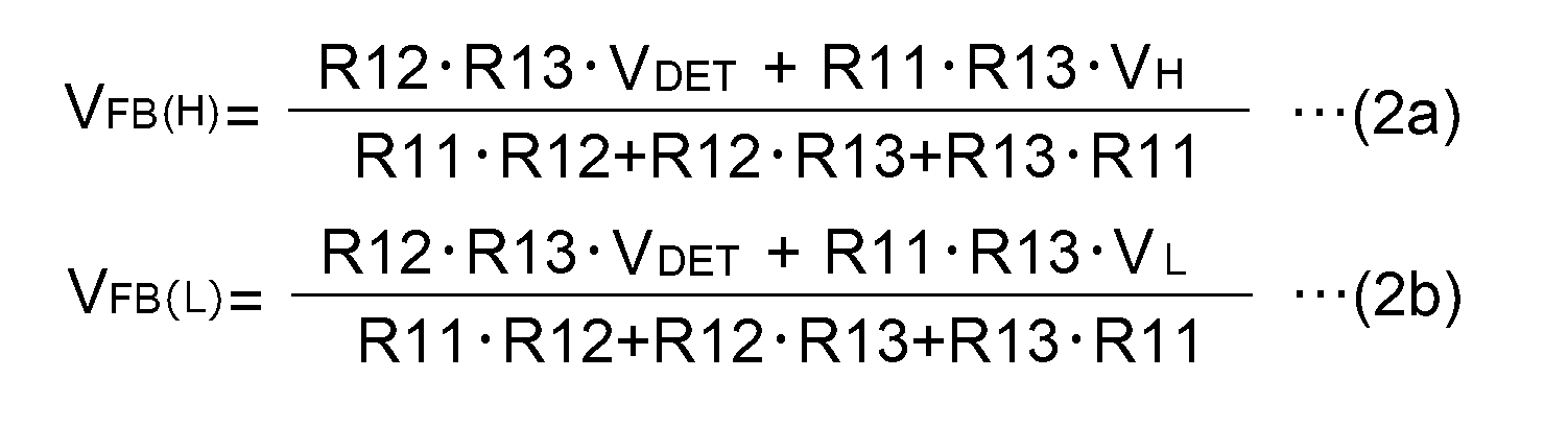
つまり、フィードバック信号VFBは、制御パルスVCTRLに応じて脈動する。ここで、脈動の周波数はfCTRLであり、コンバータコントローラ150Aのクロスオーバー周波数f0よりも高いため、脈動は、フィードバック制御に影響を与えない。その結果、フィードバック電圧VFBの平均電圧VFB(AVE)が、基準信号VREFに近づくようにフィードバックがかかる。
制御パルスVCTRLのデューティサイクルをd(0≦d≦1)とするとき、ハイ区間とロー区間の時間比率は、d:1-dとなる。そうすると、フィードバック信号VFBの時間平均値VFB(AVE)は、式(3)で表される。

式(3)に式(2a)、(2b)を代入すると、式(4)を得る。
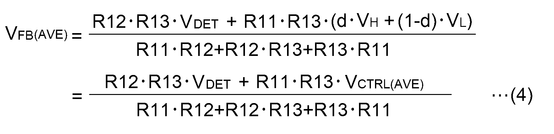
式(4)の右辺のd・VH+(1-d)・VLは、制御パルスVCTRLの時間平均値VCTRL(AVE)である。
フィードバックループが安定であるとき、VFB(AVE)=VREFが成り立ち、出力検出信号VDETの目標レベルVDET(REF)は、式(5)で表される。したがって、デューティサイクルdを変化させることにより、出力検出信号VDET、ひいては出力電圧VOUTの目標レベルを変化させることができる。

VL=0Vとすれば、目標レベルVDET(REF)は、式(6)で表される。

スイッチング電源装置100Aの利点を説明する。スイッチング電源装置100Aの利点は、比較技術との対比によって明確となる。
(比較技術1)
比較技術1では、制御パルス発生器130に代えて、D/Aコンバータが設けられる。D/Aコンバータは、目標レベルVOUT(REF)の設定値DSETを、アナログ電圧VSETに変換する。その他は、図2と同様である。
比較技術1では、制御パルス発生器130に代えて、D/Aコンバータが設けられる。D/Aコンバータは、目標レベルVOUT(REF)の設定値DSETを、アナログ電圧VSETに変換する。その他は、図2と同様である。
設定値DSETのビット数が大きい場合、高分解能なD/Aコンバータが必要となる。一般的に、高分解能なD/Aコンバータは高価である。これに対して、実施形態に係るスイッチング電源装置100Aでは、D/Aコンバータが不要であるため、コストを下げることができる。
(比較技術2)
比較技術2では、制御パルス発生器130の出力に、アナログのローパスフィルタが挿入される。これにより、フィードバック信号VFBの脈動が抑制される。
比較技術2では、制御パルス発生器130の出力に、アナログのローパスフィルタが挿入される。これにより、フィードバック信号VFBの脈動が抑制される。
比較技術2では、設定値DSETを変化させた後、ローパスフィルタの出力電圧が変化するまで、フィルタのカットオフ周波数(時定数)に応じた遅延が発生する。そのため、出力電圧VOUTの目標レベルVOUT(REF)を高速に変化させることが難しい。これに対して、実施形態では、制御パルスVCTRLがローパスフィルタを経由せずに、コンバータコントローラ150に入力される。そのため設定値DSETを変化させた後、直ちに出力電圧VOUTの目標レベルVOUT(REF)が変化することとなり、目標レベルVOUT(REF)を高速に制御できる。
なお、第3抵抗R13は省略してもよい。
本開示は、図1あるいは図2のブロック図や回路図として把握され、あるいは上述の説明から導かれるさまざまな装置、方法に及ぶものであり、特定の構成に限定されるものではない。以下、本開示の範囲を狭めるためではなく、本開示や本発明の本質や動作の理解を助け、またそれらを明確化するために、より具体的な構成例や実施例を説明する。
図3は、実施例1に係るスイッチング電源装置100Bのブロック図である。スイッチング電源装置100Bは、絶縁コンバータである。具体的には、パワー回路110Bは、フォワードコンバータであり、トランスT1、スイッチング素子M1、整流素子D1,D2、出力チョークコイルL0、出力キャパシタC0を含む。スイッチング素子M1は、トランスT1の一次巻線W1と接続される。整流素子D1,D2、出力チョークコイルL0、出力キャパシタC0は、二次巻線W2と接続される。
コンバータコントローラ150Bは、エラーアンプ152、パルス変調器154、ドライバ156、第1抵抗R11~第3抵抗R13に加えて、フォトカプラ158を備える。パルス変調器154およびドライバ156を含む一次側コントローラIC(Integrated Circuit)160は、一次側に配置される。エラーアンプ152および第1抵抗R11~第3抵抗R13は、二次側に配置される。
エラーアンプ152は、シャントレギュレータであり、フィードバック信号VFBと基準電圧VREFの誤差に応じた誤差信号IERRを、フォトカプラ158の発光素子(フォトダイオード)に供給する。パルス変調器154は、フォトカプラ158の受光素子(フォトトランジスタ)に流れる電流を、電圧信号に変換し、この電圧信号に応じたデューティサイクルを有するパルス変調信号VMODを生成する。
制御パルス発生器130とコンバータコントローラ150Bの、制御パルスVCTRLの伝送経路上には、絶縁回路132が設けられる。絶縁回路132は、フォトカプラ、パルストランス、絶縁型ゲートドライバなどの絶縁素子で構成される。
以上がスイッチング電源装置100Bの構成である。
このスイッチング電源装置100Bによれば、絶縁コンバータにおいても、出力電圧VOUTの目標レベルを高速に制御することができる。
スイッチング電源装置100Bのさらなる利点は、比較技術3との対比によって明確となる。
(比較技術3)
比較技術3は、比較技術1を絶縁コンバータに修正したものである。この場合、D/Aコンバータは、二次側に配置される。設定データDSETを一次側から二次側に伝送するために、絶縁回路が必要となるが、設定データDSETを高速伝送するためには、パラレル伝送が必要となる。設定データDSETが8ビットであるとすると、8ビットを伝送するために、8個の絶縁素子が必要となり、コストアップおよび装置の大型化という問題が生ずる。
比較技術3は、比較技術1を絶縁コンバータに修正したものである。この場合、D/Aコンバータは、二次側に配置される。設定データDSETを一次側から二次側に伝送するために、絶縁回路が必要となるが、設定データDSETを高速伝送するためには、パラレル伝送が必要となる。設定データDSETが8ビットであるとすると、8ビットを伝送するために、8個の絶縁素子が必要となり、コストアップおよび装置の大型化という問題が生ずる。
これに対して、図3の構成によれば、絶縁回路132を、1個の絶縁素子で構成できるため、コストの増加を抑え、また装置の大型化を抑えることができる。
(実施例2)
図4は、実施例2に係るスイッチング電源装置100Cのブロック図である。実施例2では、コンバータコントローラ150Cは、パルス幅変調器154Cを含み、駆動パルスVDRVは、パルス幅変調(PWM)信号である。
図4は、実施例2に係るスイッチング電源装置100Cのブロック図である。実施例2では、コンバータコントローラ150Cは、パルス幅変調器154Cを含み、駆動パルスVDRVは、パルス幅変調(PWM)信号である。
パワー回路110Cの構成は、図3のパワー回路110Bと同様である。
制御パルスVCTRLも、パルス幅変調信号である。制御パルス発生器130は、デジタルPWM回路であり、パルス幅変調器として機能するカウンタ136を含み、所定の周波数fCTRLを有する制御パルスVCTRLを生成する。
カウンタ136には、出力電圧VOUTの設定値DSETと、制御パルスVCTRLの周波数fCTRLの設定値FSETが入力される。カウンタ136は、オシレータ134が生成するクロック信号CLKをカウントすることにより、制御パルスVCTRLを生成する。具体的には、カウンタ136は、クロック信号CLKに応じてカウントアップし、カウント開始から、カウント値が設定値DSETに達するまでの間、第1レベル(たとえばハイ)を出力し、その後、カウント値が設定値FSETに達するまでの間、第2レベル(たとえばロー)を出力する。カウント値が設定値FSETに達すると、カウンタ136はリセットされ、同じ動作を繰り返す。
そして、駆動パルスVDRVの周波数、すなわちスイッチング電源装置100Cのスイッチング周波数は、制御パルスVCTRLの周波数と等しい。
たとえば、制御パルス発生器130は、制御パルスVCTRLの周期(1/fCTRL)ごとにアサートされる同期信号VSYNCを生成する。同期信号VSYNCは、パルス幅変調器154Cに供給される。パルス幅変調器154Cは、同期信号VSYNCと同期して、パルス幅変調信号VPWMを生成する。たとえばパルス幅変調器154Cは、オシレータ162と、PWMコンパレータ164を含む。オシレータ162は、同期信号VSYNCと同期して、制御パルスVCTRLの周波数と同じ周波数fCTRLを有する周期信号VOSCを生成する。周期信号VOSCは、三角波やのこぎり波である。PWMコンパレータ164は、周期信号VOSCを、誤差信号VERRと比較し、PWM信号VPWMを生成する。この構成により、PWM信号VPWMの周波数と、制御パルスVCTRLの周波数を等しくすることができる。
パワー回路110Cのスイッチング周波数と、制御パルスVCTRLの周波数がずれていると、ビートにより、出力電圧VOUTが振動する。これに対して、スイッチング周波数と制御パルスVCTRLの周波数を一致させることにより、ビートによる出力電圧の振動を抑制できる。
(実施例3)
図5は、実施例3に係るスイッチング電源装置100Dのブロック図である。スイッチング電源装置100Dにおいても、実施例2と同様に、制御パルスVCTRLと駆動パルスVDRVは両方、PWM信号である。実施例3では、制御パルスVCTRLの周波数は、駆動パルスVDRVの周波数(スイッチング周波数)のm倍または1/m倍とされる。mは自然数である。
図5は、実施例3に係るスイッチング電源装置100Dのブロック図である。スイッチング電源装置100Dにおいても、実施例2と同様に、制御パルスVCTRLと駆動パルスVDRVは両方、PWM信号である。実施例3では、制御パルスVCTRLの周波数は、駆動パルスVDRVの周波数(スイッチング周波数)のm倍または1/m倍とされる。mは自然数である。
パワー回路110Dおよびコンバータコントローラ150Dは、図4のパワー回路110C、コンバータコントローラ150Cと同様である。スイッチング電源装置100Dは、図4のスイッチング電源装置100Cに加えて、同期信号発生器140を備える。
同期信号発生器140は、制御パルス発生器130が生成する制御パルスVCTRLのm倍、または1/m倍の周波数を有する同期信号VSYNCを生成する。同期信号発生器140は、カウンタ142を含む。カウンタ142には、デジタルプロセッサ200から、同期信号VSYNCの周波数、すなわちスイッチング素子M1のスイッチング周波数を規定する周波数設定値FSET2が供給される。カウンタ142は、クロック信号CLKに応じてカウントアップし、カウント値が、周波数設定値FSET2に応じたしきい値に達すると、同期信号VSYNCをアサートし、リセットする動作を繰り返す。
この構成によれば、実施例2と同様に、ビートによる出力変動を抑制できる。
(実施例4)
図6は、実施例4に係るスイッチング電源装置100Eのブロック図である。パワー回路110Eの出力チョークコイルL0には、補助巻線L1が接続されており、補助巻線L1に発生する電圧が、出力検出信号VDETとしてコンバータコントローラ150Eに供給される。コンバータコントローラ150Eの構成は、図2のコンバータコントローラ150Aと同様である。この構成では、図3~図5のフォトカプラ158が不要である。
図6は、実施例4に係るスイッチング電源装置100Eのブロック図である。パワー回路110Eの出力チョークコイルL0には、補助巻線L1が接続されており、補助巻線L1に発生する電圧が、出力検出信号VDETとしてコンバータコントローラ150Eに供給される。コンバータコントローラ150Eの構成は、図2のコンバータコントローラ150Aと同様である。この構成では、図3~図5のフォトカプラ158が不要である。
(変形例)
上述した実施形態は例示であり、それらの各構成要素や各処理プロセスの組み合わせにいろいろな変形例が可能なことが当業者に理解される。以下、こうした変形例について説明する。
上述した実施形態は例示であり、それらの各構成要素や各処理プロセスの組み合わせにいろいろな変形例が可能なことが当業者に理解される。以下、こうした変形例について説明する。
(変形例1)
図7は、変形例1に係るスイッチング電源装置100Fのブロック図である。この変形例では、制御パルスVCTRLは、基準信号VREFに重畳される。そして、出力検出信号VDET(フィードバック信号VFB)が、基準信号VREFに制御パルスVCTRLを重畳して得られる基準信号VREF’に近づくようにフィードバックループが構成される。
図7は、変形例1に係るスイッチング電源装置100Fのブロック図である。この変形例では、制御パルスVCTRLは、基準信号VREFに重畳される。そして、出力検出信号VDET(フィードバック信号VFB)が、基準信号VREFに制御パルスVCTRLを重畳して得られる基準信号VREF’に近づくようにフィードバックループが構成される。
コンバータコントローラ150Fは、エラーアンプ152、パルス変調器154、ドライバ156、第1抵抗R21、第2抵抗R22を含む。エラーアンプ152の第1入力(+)には、第1抵抗R21および第2抵抗R22が接続される。第1抵抗R21には、基準電圧VREFが、第2抵抗R22には、制御パルスVCTRLが入力される。エラーアンプ152の第2入力には、フィードバック信号VFB(VDET)が入力される。
エラーアンプ152の第1入力には、基準電圧VREFに制御パルスVCTRLを重畳して得られる基準電圧VREF’が現れる。
VREF’=R21・VCTRL+R22・VREF/(R21+R22)
VREF’=R21・VCTRL+R22・VREF/(R21+R22)
したがって、制御パルスVCTRLのデューティサイクルを変化させることで、出力電圧VOUTの目標レベルを変化させることができる。
(変形例2)
これまでの説明では、制御パルスVCTRLが、2つの電圧レベルで変化する場合を説明したが、その限りでない。たとえば制御パルスVCTRLは、ハイインピーダンス状態HiZと、所定電圧レベルVXの二状態で変化してもよい。たとえば、図2の制御パルス発生器130あるいは、絶縁回路132は、オープンドレイン(オープンコレクタ)の出力形式を有していてもよく、この場合の所定電圧レベルVxは0Vとなる。
これまでの説明では、制御パルスVCTRLが、2つの電圧レベルで変化する場合を説明したが、その限りでない。たとえば制御パルスVCTRLは、ハイインピーダンス状態HiZと、所定電圧レベルVXの二状態で変化してもよい。たとえば、図2の制御パルス発生器130あるいは、絶縁回路132は、オープンドレイン(オープンコレクタ)の出力形式を有していてもよく、この場合の所定電圧レベルVxは0Vとなる。
本開示に係る実施形態について、具体的な用語を用いて説明したが、この説明は、理解を助けるための例示に過ぎず、本開示あるいは請求の範囲を限定するものではない。本発明の範囲は、請求の範囲によって規定されるものであり、したがって、ここでは説明しない実施形態、実施例、変形例も、本発明の範囲に含まれる。
(付記)
本明細書に開示される技術は、一側面において以下のように把握される。
本明細書に開示される技術は、一側面において以下のように把握される。
(項目1)
スイッチング素子を含むパワー回路と、
前記パワー回路の出力信号の目標値に応じたデューティサイクルを有する制御パルスを生成する制御パルス発生器と、
前記パワー回路の前記出力信号を示す出力検出信号と基準信号の誤差がゼロに近づくように、駆動パルスを生成し、前記駆動パルスに応じて前記スイッチング素子を駆動するコンバータコントローラと、
を備え、
前記制御パルスは前記出力検出信号または前記基準信号に重畳されており、前記制御パルスの周波数は、前記コンバータコントローラのクロスオーバー周波数よりも高い、スイッチング電源装置。
スイッチング素子を含むパワー回路と、
前記パワー回路の出力信号の目標値に応じたデューティサイクルを有する制御パルスを生成する制御パルス発生器と、
前記パワー回路の前記出力信号を示す出力検出信号と基準信号の誤差がゼロに近づくように、駆動パルスを生成し、前記駆動パルスに応じて前記スイッチング素子を駆動するコンバータコントローラと、
を備え、
前記制御パルスは前記出力検出信号または前記基準信号に重畳されており、前記制御パルスの周波数は、前記コンバータコントローラのクロスオーバー周波数よりも高い、スイッチング電源装置。
(項目2)
前記パワー回路は絶縁コンバータであり、
前記制御パルス発生器は、前記絶縁コンバータの一次側に設けられ、
前記コンバータコントローラは、前記絶縁コンバータの一次側と二次側に跨がって設けられ、
前記制御パルス発生器から前記コンバータコントローラの二次側のブロックへの前記制御パルスの伝送経路上に設けられた絶縁回路をさらに備える、項目1に記載のスイッチング電源装置。
前記パワー回路は絶縁コンバータであり、
前記制御パルス発生器は、前記絶縁コンバータの一次側に設けられ、
前記コンバータコントローラは、前記絶縁コンバータの一次側と二次側に跨がって設けられ、
前記制御パルス発生器から前記コンバータコントローラの二次側のブロックへの前記制御パルスの伝送経路上に設けられた絶縁回路をさらに備える、項目1に記載のスイッチング電源装置。
(項目3)
前記駆動パルスおよび前記制御パルスは、パルス幅変調信号であり、
前記駆動パルスの周波数は、前記制御パルスの周波数と等しい、項目1に記載のスイッチング電源装置。
前記駆動パルスおよび前記制御パルスは、パルス幅変調信号であり、
前記駆動パルスの周波数は、前記制御パルスの周波数と等しい、項目1に記載のスイッチング電源装置。
(項目4)
前記制御パルス発生器は、
前記パワー回路の前記出力信号の前記目標値と、前記制御パルスの周波数の設定値と、を受け、クロック信号をカウントすることにより前記制御パルスを生成するカウンタを含み、前記制御パルスの周期ごとにアサートされる同期信号を生成可能であり、
前記コンバータコントローラは、前記同期信号と同期して前記駆動パルスを生成するパルス幅変調器を含む、項目3に記載のスイッチング電源装置。
前記制御パルス発生器は、
前記パワー回路の前記出力信号の前記目標値と、前記制御パルスの周波数の設定値と、を受け、クロック信号をカウントすることにより前記制御パルスを生成するカウンタを含み、前記制御パルスの周期ごとにアサートされる同期信号を生成可能であり、
前記コンバータコントローラは、前記同期信号と同期して前記駆動パルスを生成するパルス幅変調器を含む、項目3に記載のスイッチング電源装置。
(項目5)
前記駆動パルスおよび前記制御パルスは、パルス幅変調信号であり、
mを自然数とするとき、前記駆動パルスの周波数は、前記制御パルスの周波数のm倍または1/m倍である、項目1に記載のスイッチング電源装置。
前記駆動パルスおよび前記制御パルスは、パルス幅変調信号であり、
mを自然数とするとき、前記駆動パルスの周波数は、前記制御パルスの周波数のm倍または1/m倍である、項目1に記載のスイッチング電源装置。
(項目6)
前記制御パルス発生器は、
前記パワー回路の前記出力信号の前記目標値と、前記制御パルスの周波数の設定値と、を受け、クロック信号をカウントすることにより前記制御パルスを生成する第1カウンタを含み、
前記スイッチング電源装置は、スイッチング周波数の設定値を受け、前記クロック信号をカウントすることにより同期信号を生成する第2カウンタをさらに備え、
前記コンバータコントローラは、前記同期信号と同期して前記駆動パルスを生成するパルス幅変調器を含む、項目5に記載のスイッチング電源装置。
前記制御パルス発生器は、
前記パワー回路の前記出力信号の前記目標値と、前記制御パルスの周波数の設定値と、を受け、クロック信号をカウントすることにより前記制御パルスを生成する第1カウンタを含み、
前記スイッチング電源装置は、スイッチング周波数の設定値を受け、前記クロック信号をカウントすることにより同期信号を生成する第2カウンタをさらに備え、
前記コンバータコントローラは、前記同期信号と同期して前記駆動パルスを生成するパルス幅変調器を含む、項目5に記載のスイッチング電源装置。
(項目7)
前記コンバータコントローラは、
第1入力に前記基準信号を受けるエラーアンプと、
第1端が前記エラーアンプの第2入力と接続され、第2端に前記出力検出信号を受ける第1抵抗と、
第1端が前記エラーアンプの前記第2入力と接続され、第2端に前記制御パルスを受ける第2抵抗と、
前記エラーアンプの出力である誤差信号に応じたデューティサイクルを有するパルス変調信号を生成するパルス変調器と、
を含む、項目1から6のいずれかに記載のスイッチング電源装置。
前記コンバータコントローラは、
第1入力に前記基準信号を受けるエラーアンプと、
第1端が前記エラーアンプの第2入力と接続され、第2端に前記出力検出信号を受ける第1抵抗と、
第1端が前記エラーアンプの前記第2入力と接続され、第2端に前記制御パルスを受ける第2抵抗と、
前記エラーアンプの出力である誤差信号に応じたデューティサイクルを有するパルス変調信号を生成するパルス変調器と、
を含む、項目1から6のいずれかに記載のスイッチング電源装置。
(項目8)
前記コンバータコントローラは、
第1端が前記エラーアンプの前記第2入力と接続され、第2端が接地される第3抵抗をさらに含む、項目7に記載のスイッチング電源装置。
前記コンバータコントローラは、
第1端が前記エラーアンプの前記第2入力と接続され、第2端が接地される第3抵抗をさらに含む、項目7に記載のスイッチング電源装置。
(項目9)
前記コンバータコントローラは、
第1入力に前記出力検出信号を受けるエラーアンプと、
第1端が前記エラーアンプの第2入力と接続され、第2端に前記基準信号を受ける第1抵抗と、
第1端が前記エラーアンプの前記第2入力と接続され、第2端に前記制御パルスを受ける第2抵抗と、
前記エラーアンプの出力である誤差信号に応じたデューティサイクルを有するパルス変調信号を生成するパルス変調器と、
を含む、項目1から6のいずれかに記載のスイッチング電源装置。
前記コンバータコントローラは、
第1入力に前記出力検出信号を受けるエラーアンプと、
第1端が前記エラーアンプの第2入力と接続され、第2端に前記基準信号を受ける第1抵抗と、
第1端が前記エラーアンプの前記第2入力と接続され、第2端に前記制御パルスを受ける第2抵抗と、
前記エラーアンプの出力である誤差信号に応じたデューティサイクルを有するパルス変調信号を生成するパルス変調器と、
を含む、項目1から6のいずれかに記載のスイッチング電源装置。
(項目10)
スイッチング素子を含むスイッチング電源装置の制御方法であって、
前記スイッチング電源装置の出力信号の目標値に応じたデューティサイクルを有する制御パルスを生成するステップと、
前記スイッチング電源装置の前記出力信号を示す出力検出信号に、前記制御パルスを重畳し、フィードバック信号を生成するステップと、
フィードバックコントローラによって、前記フィードバック信号と基準信号の誤差がゼロに近づくように、駆動パルスを生成するステップと、
前記駆動パルスに応じて前記スイッチング素子を駆動するステップと、
を備え、
前記制御パルスの周波数は、前記フィードバックコントローラのクロスオーバー周波数よりも高い、制御方法。
スイッチング素子を含むスイッチング電源装置の制御方法であって、
前記スイッチング電源装置の出力信号の目標値に応じたデューティサイクルを有する制御パルスを生成するステップと、
前記スイッチング電源装置の前記出力信号を示す出力検出信号に、前記制御パルスを重畳し、フィードバック信号を生成するステップと、
フィードバックコントローラによって、前記フィードバック信号と基準信号の誤差がゼロに近づくように、駆動パルスを生成するステップと、
前記駆動パルスに応じて前記スイッチング素子を駆動するステップと、
を備え、
前記制御パルスの周波数は、前記フィードバックコントローラのクロスオーバー周波数よりも高い、制御方法。
本開示は、スイッチング電源装置に関する。
2 入力電源
6 ホストコントローラ
4 負荷
100 スイッチング電源装置
102 入力ライン
104 出力ライン
110 パワー回路
C0 出力キャパシタ
D1,D2 整流素子
L0 出力チョークコイル
L1 補助巻線
M1 スイッチング素子
T1 トランス
W1 一次巻線
W2 二次巻線
130 制御パルス発生器
132 絶縁回路
136 カウンタ
140 同期信号発生器
142 カウンタ
150 コンバータコントローラ
152 エラーアンプ
154 パルス変調器
156 ドライバ
158 フォトカプラ
R11,R21 第1抵抗
R12,R22 第2抵抗
R13 第3抵抗
160 一次側コントローラIC
162 オシレータ
164 PWMコンパレータ
200 デジタルプロセッサ
6 ホストコントローラ
4 負荷
100 スイッチング電源装置
102 入力ライン
104 出力ライン
110 パワー回路
C0 出力キャパシタ
D1,D2 整流素子
L0 出力チョークコイル
L1 補助巻線
M1 スイッチング素子
T1 トランス
W1 一次巻線
W2 二次巻線
130 制御パルス発生器
132 絶縁回路
136 カウンタ
140 同期信号発生器
142 カウンタ
150 コンバータコントローラ
152 エラーアンプ
154 パルス変調器
156 ドライバ
158 フォトカプラ
R11,R21 第1抵抗
R12,R22 第2抵抗
R13 第3抵抗
160 一次側コントローラIC
162 オシレータ
164 PWMコンパレータ
200 デジタルプロセッサ
Claims (10)
- スイッチング素子を含むパワー回路と、
前記パワー回路の出力信号の目標値に応じたデューティサイクルを有する制御パルスを生成する制御パルス発生器と、
前記パワー回路の前記出力信号を示す出力検出信号と基準信号の誤差がゼロに近づくように、駆動パルスを生成し、前記駆動パルスに応じて前記スイッチング素子を駆動するコンバータコントローラと、
を備え、
前記制御パルスは前記出力検出信号または前記基準信号に重畳されており、前記制御パルスの周波数は、前記コンバータコントローラのクロスオーバー周波数よりも高い、スイッチング電源装置。 - 前記パワー回路は絶縁コンバータであり、
前記制御パルス発生器は、前記絶縁コンバータの一次側に設けられ、
前記コンバータコントローラは、前記絶縁コンバータの一次側と二次側に跨がって設けられ、
前記制御パルス発生器から前記コンバータコントローラの二次側のブロックへの前記制御パルスの伝送経路上に設けられた絶縁回路をさらに備える、請求項1に記載のスイッチング電源装置。 - 前記駆動パルスおよび前記制御パルスは、パルス幅変調信号であり、
前記駆動パルスの周波数は、前記制御パルスの周波数と等しい、請求項1に記載のスイッチング電源装置。 - 前記制御パルス発生器は、
前記パワー回路の前記出力信号の前記目標値と、前記制御パルスの周波数の設定値と、を受け、クロック信号をカウントすることにより前記制御パルスを生成するカウンタを含み、前記制御パルスの周期ごとにアサートされる同期信号を生成可能であり、
前記コンバータコントローラは、前記同期信号と同期して前記駆動パルスを生成するパルス幅変調器を含む、請求項3に記載のスイッチング電源装置。 - 前記駆動パルスおよび前記制御パルスは、パルス幅変調信号であり、
mを自然数とするとき、前記駆動パルスの周波数は、前記制御パルスの周波数のm倍または1/m倍である、請求項1に記載のスイッチング電源装置。 - 前記制御パルス発生器は、
前記パワー回路の前記出力信号の前記目標値と、前記制御パルスの周波数の設定値と、を受け、クロック信号をカウントすることにより前記制御パルスを生成する第1カウンタを含み、
前記スイッチング電源装置は、スイッチング周波数の設定値を受け、前記クロック信号をカウントすることにより同期信号を生成する第2カウンタをさらに備え、
前記コンバータコントローラは、前記同期信号と同期して前記駆動パルスを生成するパルス幅変調器を含む、請求項5に記載のスイッチング電源装置。 - 前記コンバータコントローラは、
第1入力に前記基準信号を受けるエラーアンプと、
第1端が前記エラーアンプの第2入力と接続され、第2端に前記出力検出信号を受ける第1抵抗と、
第1端が前記エラーアンプの前記第2入力と接続され、第2端に前記制御パルスを受ける第2抵抗と、
前記エラーアンプの出力である誤差信号に応じたデューティサイクルを有するパルス変調信号を生成するパルス変調器と、
を含む、請求項1から6のいずれかに記載のスイッチング電源装置。 - 前記コンバータコントローラは、
第1端が前記エラーアンプの前記第2入力と接続され、第2端が接地される第3抵抗をさらに含む、請求項7に記載のスイッチング電源装置。 - 前記コンバータコントローラは、
第1入力に前記出力検出信号を受けるエラーアンプと、
第1端が前記エラーアンプの第2入力と接続され、第2端に前記基準信号を受ける第1抵抗と、
第1端が前記エラーアンプの前記第2入力と接続され、第2端に前記制御パルスを受ける第2抵抗と、
前記エラーアンプの出力である誤差信号に応じたデューティサイクルを有するパルス変調信号を生成するパルス変調器と、
を含む、請求項1から6のいずれかに記載のスイッチング電源装置。 - スイッチング素子を含むスイッチング電源装置の制御方法であって、
前記スイッチング電源装置の出力信号の目標値に応じたデューティサイクルを有する制御パルスを生成するステップと、
前記スイッチング電源装置の前記出力信号を示す出力検出信号に、前記制御パルスを重畳し、フィードバック信号を生成するステップと、
フィードバックコントローラによって、前記フィードバック信号と基準信号の誤差がゼロに近づくように、駆動パルスを生成するステップと、
前記駆動パルスに応じて前記スイッチング素子を駆動するステップと、
を備え、
前記制御パルスの周波数は、前記フィードバックコントローラのクロスオーバー周波数よりも高い、制御方法。
Priority Applications (1)
| Application Number | Priority Date | Filing Date | Title |
|---|---|---|---|
| JP2024531967A JPWO2024009685A1 (ja) | 2022-07-04 | 2023-06-08 |
Applications Claiming Priority (2)
| Application Number | Priority Date | Filing Date | Title |
|---|---|---|---|
| JP2022-108012 | 2022-07-04 | ||
| JP2022108012 | 2022-07-04 |
Publications (1)
| Publication Number | Publication Date |
|---|---|
| WO2024009685A1 true WO2024009685A1 (ja) | 2024-01-11 |
Family
ID=89453180
Family Applications (1)
| Application Number | Title | Priority Date | Filing Date |
|---|---|---|---|
| PCT/JP2023/021403 Ceased WO2024009685A1 (ja) | 2022-07-04 | 2023-06-08 | スイッチング電源装置およびその制御方法 |
Country Status (2)
| Country | Link |
|---|---|
| JP (1) | JPWO2024009685A1 (ja) |
| WO (1) | WO2024009685A1 (ja) |
Citations (3)
| Publication number | Priority date | Publication date | Assignee | Title |
|---|---|---|---|---|
| JP2006049127A (ja) * | 2004-08-05 | 2006-02-16 | Koito Mfg Co Ltd | 照明用光源の点灯装置 |
| JP2009095091A (ja) * | 2007-10-04 | 2009-04-30 | Cosel Co Ltd | スイッチング電源装置 |
| JP2017055522A (ja) * | 2015-09-08 | 2017-03-16 | コーセル株式会社 | 電源装置及びその信号処理方法 |
-
2023
- 2023-06-08 JP JP2024531967A patent/JPWO2024009685A1/ja active Pending
- 2023-06-08 WO PCT/JP2023/021403 patent/WO2024009685A1/ja not_active Ceased
Patent Citations (3)
| Publication number | Priority date | Publication date | Assignee | Title |
|---|---|---|---|---|
| JP2006049127A (ja) * | 2004-08-05 | 2006-02-16 | Koito Mfg Co Ltd | 照明用光源の点灯装置 |
| JP2009095091A (ja) * | 2007-10-04 | 2009-04-30 | Cosel Co Ltd | スイッチング電源装置 |
| JP2017055522A (ja) * | 2015-09-08 | 2017-03-16 | コーセル株式会社 | 電源装置及びその信号処理方法 |
Also Published As
| Publication number | Publication date |
|---|---|
| JPWO2024009685A1 (ja) | 2024-01-11 |
Similar Documents
| Publication | Publication Date | Title |
|---|---|---|
| CN100588097C (zh) | 电源控制器方法和结构 | |
| CN109429413B (zh) | Led驱动设备和照明设备 | |
| US8624572B2 (en) | Switching control circuit and switching power-supply apparatus | |
| US8581505B2 (en) | Primary-side based control of secondary-side current for a transformer | |
| TWI434504B (zh) | 用以控制降升壓型轉換器操作之裝置、控制電路、方法 | |
| US9154031B2 (en) | Current mode DC-DC conversion device with fast transient response | |
| US7952426B2 (en) | Digital audio amplifier and digital audio amplifying method therefor | |
| JP5304745B2 (ja) | 絶縁型電源装置および照明装置 | |
| US8233292B2 (en) | Controllers, systems and methods for controlling power of light sources | |
| JP6220249B2 (ja) | スイッチングコンバータおよびその制御回路、ac/dcコンバータ、電源アダプタおよび電子機器 | |
| US9397517B2 (en) | Cable compensation by zero-crossing compensation current and resistor | |
| KR20120066603A (ko) | Dc/dc 컨버터와 그것을 이용한 전원 장치 및 전자 기기 | |
| JP2001119929A (ja) | 電源モジュール | |
| RU2698301C2 (ru) | Управляемый драйвер и способ возбуждения | |
| CN107612336A (zh) | 用于谐振转换器的可变消隐频率 | |
| CN110601537B (zh) | 初级侧恒定电流调节 | |
| CN102751864B (zh) | 基于Cuk的电流源 | |
| JP4198588B2 (ja) | 制御ループを具える回路形態 | |
| WO2021134752A1 (en) | Current mode dc-dc converter | |
| TW201904184A (zh) | 直流對直流轉換電路及其多相電源控制器 | |
| CN110611432B (zh) | 开关变换器的控制电路及控制方法 | |
| CN114499191A (zh) | 功率变换器 | |
| TW200824250A (en) | Loading variation compensation circuit for a switching-mode power converter, and switching-mode power converter and conversion using the same | |
| WO2024009685A1 (ja) | スイッチング電源装置およびその制御方法 | |
| WO2024014201A1 (ja) | スイッチング電源装置およびその制御方法 |
Legal Events
| Date | Code | Title | Description |
|---|---|---|---|
| 121 | Ep: the epo has been informed by wipo that ep was designated in this application |
Ref document number: 23835221 Country of ref document: EP Kind code of ref document: A1 |
|
| WWE | Wipo information: entry into national phase |
Ref document number: 2024531967 Country of ref document: JP |
|
| NENP | Non-entry into the national phase |
Ref country code: DE |
|
| 122 | Ep: pct application non-entry in european phase |
Ref document number: 23835221 Country of ref document: EP Kind code of ref document: A1 |