WO2023286545A1 - Lamp - Google Patents
Lamp Download PDFInfo
- Publication number
- WO2023286545A1 WO2023286545A1 PCT/JP2022/024852 JP2022024852W WO2023286545A1 WO 2023286545 A1 WO2023286545 A1 WO 2023286545A1 JP 2022024852 W JP2022024852 W JP 2022024852W WO 2023286545 A1 WO2023286545 A1 WO 2023286545A1
- Authority
- WO
- WIPO (PCT)
- Prior art keywords
- temperature
- circuit
- voltage
- signal
- detection circuit
- Prior art date
Links
- 238000001514 detection method Methods 0.000 claims abstract description 203
- 239000000758 substrate Substances 0.000 claims abstract description 33
- 230000010355 oscillation Effects 0.000 claims description 32
- 238000006243 chemical reaction Methods 0.000 claims description 24
- 239000003990 capacitor Substances 0.000 description 40
- 238000010586 diagram Methods 0.000 description 31
- 230000020169 heat generation Effects 0.000 description 14
- 230000006378 damage Effects 0.000 description 11
- 101000746134 Homo sapiens DNA endonuclease RBBP8 Proteins 0.000 description 10
- 101000969031 Homo sapiens Nuclear protein 1 Proteins 0.000 description 10
- 102100021133 Nuclear protein 1 Human genes 0.000 description 10
- 230000007423 decrease Effects 0.000 description 4
- 230000036039 immunity Effects 0.000 description 4
- 230000003044 adaptive effect Effects 0.000 description 3
- 230000000694 effects Effects 0.000 description 2
- 238000000034 method Methods 0.000 description 2
- 230000001360 synchronised effect Effects 0.000 description 2
Images


Classifications
-
- H—ELECTRICITY
- H05—ELECTRIC TECHNIQUES NOT OTHERWISE PROVIDED FOR
- H05B—ELECTRIC HEATING; ELECTRIC LIGHT SOURCES NOT OTHERWISE PROVIDED FOR; CIRCUIT ARRANGEMENTS FOR ELECTRIC LIGHT SOURCES, IN GENERAL
- H05B45/00—Circuit arrangements for operating light-emitting diodes [LED]
- H05B45/50—Circuit arrangements for operating light-emitting diodes [LED] responsive to malfunctions or undesirable behaviour of LEDs; responsive to LED life; Protective circuits
- H05B45/56—Circuit arrangements for operating light-emitting diodes [LED] responsive to malfunctions or undesirable behaviour of LEDs; responsive to LED life; Protective circuits involving measures to prevent abnormal temperature of the LEDs
-
- F—MECHANICAL ENGINEERING; LIGHTING; HEATING; WEAPONS; BLASTING
- F21—LIGHTING
- F21S—NON-PORTABLE LIGHTING DEVICES; SYSTEMS THEREOF; VEHICLE LIGHTING DEVICES SPECIALLY ADAPTED FOR VEHICLE EXTERIORS
- F21S41/00—Illuminating devices specially adapted for vehicle exteriors, e.g. headlamps
- F21S41/10—Illuminating devices specially adapted for vehicle exteriors, e.g. headlamps characterised by the light source
- F21S41/14—Illuminating devices specially adapted for vehicle exteriors, e.g. headlamps characterised by the light source characterised by the type of light source
- F21S41/141—Light emitting diodes [LED]
-
- F—MECHANICAL ENGINEERING; LIGHTING; HEATING; WEAPONS; BLASTING
- F21—LIGHTING
- F21S—NON-PORTABLE LIGHTING DEVICES; SYSTEMS THEREOF; VEHICLE LIGHTING DEVICES SPECIALLY ADAPTED FOR VEHICLE EXTERIORS
- F21S45/00—Arrangements within vehicle lighting devices specially adapted for vehicle exteriors, for purposes other than emission or distribution of light
- F21S45/10—Protection of lighting devices
-
- H—ELECTRICITY
- H05—ELECTRIC TECHNIQUES NOT OTHERWISE PROVIDED FOR
- H05B—ELECTRIC HEATING; ELECTRIC LIGHT SOURCES NOT OTHERWISE PROVIDED FOR; CIRCUIT ARRANGEMENTS FOR ELECTRIC LIGHT SOURCES, IN GENERAL
- H05B45/00—Circuit arrangements for operating light-emitting diodes [LED]
- H05B45/10—Controlling the intensity of the light
- H05B45/14—Controlling the intensity of the light using electrical feedback from LEDs or from LED modules
-
- H—ELECTRICITY
- H05—ELECTRIC TECHNIQUES NOT OTHERWISE PROVIDED FOR
- H05B—ELECTRIC HEATING; ELECTRIC LIGHT SOURCES NOT OTHERWISE PROVIDED FOR; CIRCUIT ARRANGEMENTS FOR ELECTRIC LIGHT SOURCES, IN GENERAL
- H05B45/00—Circuit arrangements for operating light-emitting diodes [LED]
- H05B45/10—Controlling the intensity of the light
- H05B45/18—Controlling the intensity of the light using temperature feedback
-
- H—ELECTRICITY
- H05—ELECTRIC TECHNIQUES NOT OTHERWISE PROVIDED FOR
- H05B—ELECTRIC HEATING; ELECTRIC LIGHT SOURCES NOT OTHERWISE PROVIDED FOR; CIRCUIT ARRANGEMENTS FOR ELECTRIC LIGHT SOURCES, IN GENERAL
- H05B45/00—Circuit arrangements for operating light-emitting diodes [LED]
- H05B45/30—Driver circuits
- H05B45/305—Frequency-control circuits
-
- H—ELECTRICITY
- H05—ELECTRIC TECHNIQUES NOT OTHERWISE PROVIDED FOR
- H05B—ELECTRIC HEATING; ELECTRIC LIGHT SOURCES NOT OTHERWISE PROVIDED FOR; CIRCUIT ARRANGEMENTS FOR ELECTRIC LIGHT SOURCES, IN GENERAL
- H05B45/00—Circuit arrangements for operating light-emitting diodes [LED]
- H05B45/30—Driver circuits
- H05B45/32—Pulse-control circuits
- H05B45/325—Pulse-width modulation [PWM]
-
- H—ELECTRICITY
- H05—ELECTRIC TECHNIQUES NOT OTHERWISE PROVIDED FOR
- H05B—ELECTRIC HEATING; ELECTRIC LIGHT SOURCES NOT OTHERWISE PROVIDED FOR; CIRCUIT ARRANGEMENTS FOR ELECTRIC LIGHT SOURCES, IN GENERAL
- H05B45/00—Circuit arrangements for operating light-emitting diodes [LED]
- H05B45/30—Driver circuits
- H05B45/37—Converter circuits
- H05B45/3725—Switched mode power supply [SMPS]
- H05B45/375—Switched mode power supply [SMPS] using buck topology
-
- H—ELECTRICITY
- H05—ELECTRIC TECHNIQUES NOT OTHERWISE PROVIDED FOR
- H05B—ELECTRIC HEATING; ELECTRIC LIGHT SOURCES NOT OTHERWISE PROVIDED FOR; CIRCUIT ARRANGEMENTS FOR ELECTRIC LIGHT SOURCES, IN GENERAL
- H05B45/00—Circuit arrangements for operating light-emitting diodes [LED]
- H05B45/30—Driver circuits
- H05B45/37—Converter circuits
- H05B45/3725—Switched mode power supply [SMPS]
- H05B45/38—Switched mode power supply [SMPS] using boost topology
-
- H—ELECTRICITY
- H05—ELECTRIC TECHNIQUES NOT OTHERWISE PROVIDED FOR
- H05B—ELECTRIC HEATING; ELECTRIC LIGHT SOURCES NOT OTHERWISE PROVIDED FOR; CIRCUIT ARRANGEMENTS FOR ELECTRIC LIGHT SOURCES, IN GENERAL
- H05B45/00—Circuit arrangements for operating light-emitting diodes [LED]
- H05B45/30—Driver circuits
- H05B45/37—Converter circuits
- H05B45/3725—Switched mode power supply [SMPS]
- H05B45/39—Circuits containing inverter bridges
-
- H—ELECTRICITY
- H05—ELECTRIC TECHNIQUES NOT OTHERWISE PROVIDED FOR
- H05B—ELECTRIC HEATING; ELECTRIC LIGHT SOURCES NOT OTHERWISE PROVIDED FOR; CIRCUIT ARRANGEMENTS FOR ELECTRIC LIGHT SOURCES, IN GENERAL
- H05B45/00—Circuit arrangements for operating light-emitting diodes [LED]
- H05B45/30—Driver circuits
- H05B45/395—Linear regulators
-
- H—ELECTRICITY
- H05—ELECTRIC TECHNIQUES NOT OTHERWISE PROVIDED FOR
- H05B—ELECTRIC HEATING; ELECTRIC LIGHT SOURCES NOT OTHERWISE PROVIDED FOR; CIRCUIT ARRANGEMENTS FOR ELECTRIC LIGHT SOURCES, IN GENERAL
- H05B45/00—Circuit arrangements for operating light-emitting diodes [LED]
- H05B45/40—Details of LED load circuits
- H05B45/44—Details of LED load circuits with an active control inside an LED matrix
- H05B45/46—Details of LED load circuits with an active control inside an LED matrix having LEDs disposed in parallel lines
-
- H—ELECTRICITY
- H05—ELECTRIC TECHNIQUES NOT OTHERWISE PROVIDED FOR
- H05B—ELECTRIC HEATING; ELECTRIC LIGHT SOURCES NOT OTHERWISE PROVIDED FOR; CIRCUIT ARRANGEMENTS FOR ELECTRIC LIGHT SOURCES, IN GENERAL
- H05B47/00—Circuit arrangements for operating light sources in general, i.e. where the type of light source is not relevant
- H05B47/10—Controlling the light source
- H05B47/105—Controlling the light source in response to determined parameters
-
- H—ELECTRICITY
- H05—ELECTRIC TECHNIQUES NOT OTHERWISE PROVIDED FOR
- H05B—ELECTRIC HEATING; ELECTRIC LIGHT SOURCES NOT OTHERWISE PROVIDED FOR; CIRCUIT ARRANGEMENTS FOR ELECTRIC LIGHT SOURCES, IN GENERAL
- H05B47/00—Circuit arrangements for operating light sources in general, i.e. where the type of light source is not relevant
- H05B47/10—Controlling the light source
- H05B47/165—Controlling the light source following a pre-assigned programmed sequence; Logic control [LC]
-
- H—ELECTRICITY
- H05—ELECTRIC TECHNIQUES NOT OTHERWISE PROVIDED FOR
- H05B—ELECTRIC HEATING; ELECTRIC LIGHT SOURCES NOT OTHERWISE PROVIDED FOR; CIRCUIT ARRANGEMENTS FOR ELECTRIC LIGHT SOURCES, IN GENERAL
- H05B47/00—Circuit arrangements for operating light sources in general, i.e. where the type of light source is not relevant
- H05B47/10—Controlling the light source
- H05B47/175—Controlling the light source by remote control
- H05B47/18—Controlling the light source by remote control via data-bus transmission
-
- H—ELECTRICITY
- H05—ELECTRIC TECHNIQUES NOT OTHERWISE PROVIDED FOR
- H05B—ELECTRIC HEATING; ELECTRIC LIGHT SOURCES NOT OTHERWISE PROVIDED FOR; CIRCUIT ARRANGEMENTS FOR ELECTRIC LIGHT SOURCES, IN GENERAL
- H05B47/00—Circuit arrangements for operating light sources in general, i.e. where the type of light source is not relevant
- H05B47/20—Responsive to malfunctions or to light source life; for protection
- H05B47/28—Circuit arrangements for protecting against abnormal temperature
Definitions
- This disclosure relates to lighting fixtures.
- ADB Adaptive Driving Beam
- the present disclosure has been made in view of the conventional problems as described above, and an object thereof is to provide a lighting fixture capable of suppressing heat generation and preventing destruction of electronic components.
- the lighting fixture of the present disclosure includes: a power supply circuit provided on a first substrate for generating a predetermined voltage based on a power supply voltage; a plurality of light emitting elements provided on a second substrate; a light source that uses the predetermined voltage as a power source; a control unit that is provided on a third substrate and controls the adjustment unit; and the first substrate.
- a first temperature detection circuit provided on the second substrate for detecting temperature
- a second temperature detection circuit provided on the second substrate for detecting temperature
- the adjustment unit is controlled based on the detection result of the higher temperature among the detection results of the detection circuits and the signal indicating the lighting condition of the plurality of light emitting elements.
- the lighting device of the present disclosure includes a power supply circuit that generates a predetermined voltage based on a power supply voltage, a plurality of light emitting elements, and a drive current that flows through each of the plurality of light emitting elements.
- a light source powered by the predetermined voltage;
- a temperature detection circuit provided on a substrate on which the power supply circuit is arranged to detect temperature;
- a second signal indicating lighting conditions of the plurality of light emitting elements;
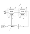
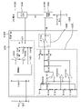
- FIG. 1 is a block diagram showing an example of a system configuration including a vehicle lamp 1 according to a first embodiment
- FIG. 3 is a block diagram showing the configuration of an ADB unit 5 in the first embodiment
- FIG. 3 is a diagram showing a configuration example of a circuit arranged on a power supply substrate K1 shown in FIG. 2
- FIG. 3 is a diagram showing a configuration example of a circuit arranged on an LED board K2 shown in FIG. 2
- FIG. It is a figure for demonstrating the relationship between the temperature information and temperature derating in 1st Embodiment. It is a figure for demonstrating the relationship between the temperature information and temperature derating in 1st Embodiment.
- FIG. 11 is a block diagram showing an example of a system configuration including a vehicle lamp 1001 of a third embodiment
- FIG. 13 is a diagram showing a configuration example of an ADB unit 1005 in the third embodiment
- FIG. 10 is a diagram showing the configuration of a detection circuit 1050 according to the third embodiment
- FIG. 4 is a diagram for explaining the relationship between temperature information of a temperature detection circuit 1051 and temperature derating
- FIG. 4 is a diagram for explaining the relationship between temperature information of a temperature detection circuit 1051 and temperature derating
- FIG. 4 is a diagram for explaining the relationship between temperature information of a temperature detection circuit 1051 and temperature derating
- FIG. 12 is a diagram showing the configuration of a detection circuit 1150 according to the fourth embodiment
- FIG. FIG. 12 is a diagram showing the configuration of a detection circuit 1250 according to the fifth embodiment
- FIG. FIG. 23 is a diagram showing the configuration of a detection circuit 1350 according to the sixth embodiment
- FIG. 4 is a diagram for explaining the relationship between temperature information of a temperature detection circuit 1055 and temperature derating;
- FIG. 4 is a diagram for explaining the relationship between temperature information of a temperature detection circuit 1055 and temperature derating;
- FIG. 4 is a diagram for explaining the relationship between temperature information of a temperature detection circuit 1055 and temperature derating;
- FIG. 4 is a diagram for explaining the relationship between temperature information of a temperature detection circuit 1055 and temperature derating;
- FIG. 4 is a diagram for explaining the relationship between temperature information of a temperature detection circuit 1055 and temperature derating;
- FIG. 4 is a diagram for explaining the relationship between temperature information of a temperature detection circuit 1055 and temperature derating;
- the system shown in FIG. 1 includes a vehicle ECU (Electronic Control Unit) 10 provided on the vehicle side and a vehicle lamp 1 on the lamp side.
- ECU Electronic Control Unit
- the vehicle ECU 10 is connected to the lighting ECU 2 of the vehicle lighting 1 on the lamp side via a control line such as a CAN (Controller Area Network), and controls the vehicle lighting 1 in an integrated manner.
- the vehicle ECU 10 of the present embodiment receives vehicle information from the driver's seat of the vehicle and camera information from the vehicle-mounted camera, and based on the information, sends a signal for controlling the vehicle lamp 1 to the lamp ECU 2 .
- the vehicle lamp 1 is, for example, a headlamp provided at the front end of the vehicle, and corresponds to a "lamp".
- the vehicular lamp 1 is provided on the right side and the left side of the vehicle, respectively, but since the left and right sides have the same configuration, FIG. 1 shows the configuration of only one side (for example, the right side).
- the vehicle lamp 1 of this embodiment includes a lamp ECU 2 , a Lo light source 3 , a Hi light source 4 and an ADB unit 5 .
- the lamp ECU 2 is a device that controls lighting of each light source of the vehicle lamp 1 .
- a signal including vehicle information, camera information, and the like is input from the vehicle ECU 10 to the lamp ECU 2 . Based on this signal, the lamp ECU 2 appropriately lights the Lo light source 3, the Hi light source 4, and the ADB light source 30 (described later) of the ADB unit 5.
- FIG. The lamp ECU 2 transmits a signal SA indicating lighting conditions (such as a light distribution pattern) of the ADB light source 30 to a control circuit 40 (described later) of the ADB unit 5 .
- the lamp ECU 2 is supplied with a power supply line with a power supply voltage Vbat from a vehicle battery (battery 6 shown in FIG. 2) and a ground line with a ground level voltage.
- the lamp ECU 2 supplies power to the Lo light source 3 , the Hi light source 4 and the ADB unit 5 .
- the Lo light source 3 is a low beam light source.
- the low beam illuminates the vicinity of the vehicle with a predetermined illuminance, and is used mainly when driving in an urban area.
- the Hi light source 4 is a high beam light source.
- the high beam illuminates a wide and distant area in front of the vehicle with relatively high illuminance, and is mainly used for high-speed driving on roads with few oncoming and preceding vehicles.
- the ADB unit 5 is a unit that constitutes a variable light distribution headlamp (ADB: Adaptive Driving Beam) that variably controls the light distribution of the light distribution pattern.
- ADB uses an in-vehicle camera to detect the presence of preceding vehicles, oncoming vehicles, and pedestrians in front of the vehicle. is intended to reduce
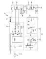
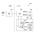
- FIG. 2 is a block diagram showing the configuration of the ADB unit 5 in the first embodiment.
- 3 is a diagram showing a configuration example of a circuit arranged on the power supply board K1 shown in FIG. 2
- FIG. 4 is a diagram showing a configuration example of a circuit arranged on the LED board K2 shown in FIG. be.
- the ADB unit 5 of this embodiment includes a power board K1, an LED board K2, and a controller board K3. Further, the power supply circuit 20 and the detection circuit 50 are arranged on the power supply board K1, the ADB light source 30 and the detection circuit 60 are arranged on the LED board K2, and the control circuit 40 is arranged on the controller board K3. ing.
- the power supply board K1 corresponds to the "first board”
- the LED board K2 corresponds to the "second board”
- the controller board K3 corresponds to the "third board”.
- each substrate is connected by a signal line such as a harness.
- the power supply circuit 20 is a voltage regulator that generates a predetermined voltage (eg 5V) based on the power supply voltage Vbat (eg 12V) supplied from the battery 6 of the vehicle.
- the power supply circuit 20 of this embodiment is a step-down DC-DC converter (for example, a switching regulator).
- a linear regulator may be used, or a configuration including a booster circuit and a step-down circuit (a configuration in which the voltage is stepped up after being stepped up) may be used.
- the power supply circuit 20 is a so-called synchronous rectification type circuit, and as shown in FIG. there is
- the capacitor C1 is an input-side capacitor, one end of which is connected to the power supply line and the other end of which is connected (grounded) to the ground line.
- the transistors M1 and M2 are NMOSFETs, the drain of the transistor M1 is connected to one end of the capacitor C1, and the source of the transistor M1 is connected to the drain of the transistor M2 and one end of the coil L1. The source of transistor M2 is grounded. Gates of the transistors M1 and M2 are connected to the control IC 21, and the transistors M1 and M2 are controlled to be turned on and off by the control IC21.
- the other end of the coil L1 is connected to one end of a capacitor C2 on the output side via a resistor R1. Also, the other end of the capacitor C2 is grounded. The voltage generated across the capacitor C2 is the output voltage.
- the resistors R2 and R3 are connected in series between the connection point between the resistor R1 and one end of the capacitor C2 and the ground. Also, the voltage at the connection point between the resistors R2 and R3 (the voltage obtained by dividing the output voltage by the resistors R2 and R3) is taken into the control IC 21 .
- the control IC 21 switches the transistors M1 and M2 based on the voltage generated at the connection point between the resistors R2 and R3 so that the output voltage of the power supply circuit 20 becomes a predetermined voltage.
- the input voltage (the voltage of the capacitor C1) is applied to one end of the coil L1.
- the ground line voltage (ground voltage) is applied to one end of the coil L1.
- the output voltage of the power supply circuit 20 becomes lower than the input voltage (power supply voltage Vbat) and is controlled to a predetermined voltage (eg, 5V).
- the ADB light source 30 is a light source powered by the output voltage (predetermined voltage) of the power supply circuit 20, and corresponds to a "light source”.
- the ADB light source 30 includes a plurality (N) of light emitting elements D1 to DN, a plurality (N) of current sources 31_1 to 31_N, and a light distribution adjustment circuit 32.
- the plurality of light emitting elements D1 to DN and the plurality of current sources 31_1 to 31_N are connected in series between the power line and the ground line, respectively. That is, in the ADB light source 30, a plurality of combinations of series-connected light-emitting elements and current sources are arranged in parallel (connected in parallel).
- the light-emitting elements D1 to DN are elements that are lit by being supplied with a drive current, and LEDs (light-emitting diodes) are used in this embodiment.
- the plurality of light emitting elements D1 to DN are connected in parallel and arranged side by side, for example, in an array so as to form a light distribution pattern.
- the current sources 31_1 to 31_N supply drive currents to the corresponding light emitting elements.
- the light distribution adjustment circuit 32 controls the current sources 31_1 to 31_N in accordance with instructions from the control circuit 40 (signal SC input from the control circuit 40), and adjusts the drive currents flowing through the plurality of light emitting elements D1 to DN. . Thereby, lighting can be performed with a light distribution pattern according to the situation of the vehicle. Note that the light distribution adjustment circuit 32 corresponds to an "adjustment unit".
- the method of adjusting the drive current by the light distribution adjustment circuit 32 is not particularly limited, and for example, PWM control or analog control can be applied.
- the current sources 31_1 to 31_N are configured by current mirror circuits, and by adjusting the magnitude of the drive current flowing through one light emitting element, the magnitude of the dynamic current flowing through the other light emitting elements can be adjusted accordingly. I am trying to change.
- Control circuit 40 Based on a signal SA from the lamp ECU 2 (and signals SB1 and SB2 from detection circuits 50 and 60, which will be described later), the control circuit 40 collectively instructs the lighting and extinguishing of the plurality of light emitting elements D1 to DN, the luminance pattern, and the like.
- a signal SC is generated and output to the light distribution adjustment circuit 32 of the ADB light source 30 .
- the control circuit 40 controls the light distribution adjustment circuit 32 to light the plurality of light emitting elements D1 to DN with desired brightness.
- the control circuit 40 corresponds to a "control section".
- the ADB light source 30 of this embodiment a plurality of light emitting elements D1 to DN are connected in parallel.
- the larger the number of light-emitting elements to be lit the larger the current required.
- the power supply circuit 20 that supplies power and the ADB light source 30 generate a large amount of heat, which may cause thermal destruction of the electronic components.
- the power board K1 on which the power supply circuit 20 is arranged is provided with the detection circuit 50 capable of detecting the temperature
- the LED board K2 on which the ADB light source 30 is arranged is provided with the detection circuit 50 capable of detecting the temperature.
- a circuit 60 is provided. Then, based on one of the detection result of the detection circuit 50 and the detection result of the detection circuit 60 (the one with the higher temperature) and the signal SA indicating the lighting condition from the lamp ECU 2, the power consumption increases according to the temperature rise. Temperature derating is performed to lower the
- the detection circuit 50 is provided on the power supply board K ⁇ b>1 on which the power supply circuit 20 is arranged, and has a temperature detection circuit 51 and an interface circuit (hereinafter, I/F circuit) 52 .
- the temperature detection circuit 51 is a circuit that is provided on the power supply board K1 and detects temperature. Note that the temperature detection circuit 51 corresponds to a "first temperature detection circuit".
- the temperature detection circuit 51 of this embodiment is composed of an oscillation circuit that outputs a signal SD1 having a frequency corresponding to temperature. As shown in FIG. 3, the temperature detection circuit 51 includes resistors R4 to R6, capacitors C3 and C4, a thermistor Rth1, and an operational amplifier OP1.
- the resistors R4 and R5 are connected in series, one end (one end of the resistor R4) is applied with the voltage Vcc, and the other end (the other end of the resistor R5) is grounded.
- One end of the capacitor C3 is connected to the connection point between the series-connected resistors R4 and R5, and the other end is grounded.
- the inverting input terminal (-terminal) of the operational amplifier OP1 is grounded through the capacitor C4 and connected to the output of the operational amplifier OP1 through the thermistor Rth1.
- the thermistor Rth1 is an electronic component whose resistance value changes according to changes in temperature (see FIG. 5).
- non-inverting input terminal (+ terminal) of the operational amplifier OP1 is connected to the connection point between the resistors R4 and R5, and is also connected to the output of the operational amplifier OP1 via the resistor R6.
- This temperature detection circuit 51 is obtained by replacing part of the resistance (the resistance connected between the - terminal and the output) with a thermistor Rth1 in the oscillation circuit using the operational amplifier OP1.
- the frequency of the output signal (signal SD1) changes as the resistance value of the thermistor Rth1 changes according to the temperature.
- a Hartley oscillation circuit or a Wien bridge oscillation circuit for example, may be used as long as it can output a signal SD having a frequency corresponding to the resistance value of the thermistor Rth1.
- the I/F circuit 52 is a circuit that converts the output signal (signal SD1) of the temperature detection circuit 51 into a logic level signal (signal SB1).
- a logic level signal is a square-wave signal that switches between a high level (H level hereinafter) and a low level (L level hereinafter). Note that the I/F circuit 52 corresponds to the "first interface circuit".
- the I/F circuit 52 includes a transistor M3, resistors R7 to R9, a coil L2, and a capacitor C5. Also, the coil L2 and the capacitor C5 are connected to a pull-up resistor (not shown) inside the control circuit 40 .
- the transistor M3 is an NPN transistor whose emitter is grounded and whose collector is connected to one end of the coil L2 via a resistor R9. Power is supplied from the control circuit 40, for example, to the collector of the NPN transistor M3.
- the base of the NPN transistor M3 is connected to the connection point between the resistors R7 and R8 which are connected in series between the output of the temperature detection circuit 51 (the output of the operational amplifier OP1) and the ground. That is, the voltage obtained by dividing the output (signal SD1) of the temperature detection circuit 51 by the resistors R7 and R8 is applied to the base of the NPN transistor M3.
- One end of the capacitor C5 is connected to the other end of the coil L2, and the other end of the capacitor C5 is grounded.
- the coil L2 and the capacitor C5 constitute a filter for removing noise. Also, the voltage across the capacitor C5 is the output of the detection circuit 50. FIG.
- the output (signal SB1) of the I/F circuit 52 becomes a rectangular wave signal (logical level signal) indicating the temperature information based on the signal SD1.
- the signal SB1 is a rectangular wave, making it less susceptible to noise (increasing noise resistance).
- the detection circuit 60 is provided on the LED board K2 on which the ADB light source 30 is arranged, and has a temperature detection circuit 61 and an I/F circuit 62 .
- the temperature detection circuit 61 is a circuit that is provided on the LED board K2 and detects temperature. Note that the temperature detection circuit 61 corresponds to a "second temperature detection circuit".
- the temperature detection circuit 61 of this embodiment is composed of an oscillation circuit that outputs a signal SD2 having a frequency corresponding to temperature. As shown in FIG. 4, the temperature detection circuit 61 includes resistors R10 to R12, capacitors C6 and C7, a thermistor Rth2, and an operational amplifier OP2. Note that the configuration of the temperature detection circuit 61 is the same as that of the temperature detection circuit 51, so description thereof will be omitted.
- the I/F circuit 62 is a circuit that converts the output signal (signal SD2) of the temperature detection circuit 61 into a logic level signal (signal SB2). Note that the I/F circuit 62 corresponds to a "second interface circuit".
- the I/F circuit 62 has a transistor M4, resistors R13 to R15, a coil L3, and a capacitor C8. Also, the coil L3 and the capacitor C8 are connected to a pull-up resistor (not shown) inside the control circuit 40 . Since the configuration of the I/F circuit 62 is the same as that of the I/F circuit 52, the description thereof will be omitted.
- the control circuit 40 detects one of the detection result of the detection circuit 50 (in other words, the temperature detection circuit 51) and the detection result of the detection circuit 60 (in other words, the temperature detection circuit 61), and the light distribution pattern (lighting condition) from the lamp ECU 2. ) and the temperature derating is performed.
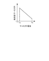
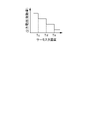
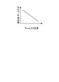
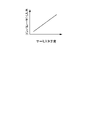
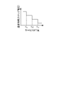
- FIGS. 5 to 7 are diagrams for explaining the relationship between temperature information and temperature derating in the first embodiment.
- the horizontal axes of FIGS. 5 to 7 indicate the temperature of the thermistor Rth1.
- the vertical axis of FIG. 5 represents the resistance value of the thermistor Rth1
- the vertical axis of FIG. 6 represents temperature information (the oscillation frequency of the signal SD1) of the temperature detection circuit 51, and the vertical axis of FIG. It shows the magnitude of the output current (driving current flowing through the light emitting element) in the light source 30 .
- the resistance value of the thermistor Rth1 decreases as the temperature rises.
- the oscillation frequency of the signal SD1 increases as the temperature rises.
- the oscillation frequency of signal SD2 increases as the temperature rises.
- the control circuit 40 selects the signal SB1 received from the detection circuit 50 or the signal SB2 received from the detection circuit 60, whichever has the higher frequency (in other words, the one with the higher temperature). Then, temperature derating is performed as shown in FIG. 7 based on the detection result of the higher temperature and the signal SA indicating the lighting condition. That is, it generates a signal SC that reduces the power consumption (driving current flowing through the light emitting element) as the frequency rises (the temperature rises), and controls the light distribution adjustment circuit 32 .
- the control circuit 40 when performing temperature derating, is arranged so that the drive current flowing through each of the light emitting elements D1 to DN is small without changing the number of light emitting elements D1 to DN to be lit. It controls the light adjustment circuit 32 . As a result, power consumption can be reduced (heat generation can be suppressed) without affecting the light distribution pattern.
- the present invention is not limited to this, and for example, the upper limit of the drive current flowing through each light emitting element may be lowered, or the light distribution pattern may be changed. By doing so, it is possible to efficiently suppress heat generation in the power supply board K1 and the LED board K2, and to prevent destruction of electronic components.
- the temperature information (frequency) range (range corresponding to temperatures Ta to Tb) for temperature derating is designed in accordance with the specifications of the control circuit 40, which is the information receiving side. If this temperature range is wide and the oscillation operation becomes unstable, a temperature detection circuit (not shown) that serves as a trigger is provided on the power supply board K1 and the LED board K2 separately from the oscillation circuit. , the temperature derating may be performed or stopped.
- FIG. 8 is a diagram showing the configuration of the ADB unit 15 of the second embodiment.
- parts having the same configuration as in the first embodiment are denoted by the same reference numerals, and descriptions thereof are omitted.
- the power supply circuit 20 and the detection circuit 150 are arranged on the power supply board K1
- the ADB light source 30 and the detection circuit 160 are arranged on the LED board K2
- the control circuit 40 and the voltage conversion circuit 70 (and A buffer circuit 71) is arranged.
- the detection circuit 150 is provided on the power supply board K1 and includes a temperature detection circuit 53 for detecting temperature and a buffer circuit 54 .
- the temperature detection circuit 53 includes a resistor R16 and a thermistor Rth3.
- the resistor R16 and the thermistor Rth3 are connected in series, one end (the end of the thermistor Rth3) is applied with the voltage Vcc, and the other end (the end of the resistor R16) is grounded.
- the temperature detection circuit 53 corresponds to the "first temperature detection circuit”.
- the buffer circuit 54 is a circuit that prevents the output voltage from fluctuating according to the input impedance, and is composed of an operational amplifier OP3 (voltage follower) whose output is negatively fed back.
- the output voltage of the temperature detection circuit 53 (the voltage at the connection node of the resistor R16 and the thermistor Rth3) is applied to the + terminal of the operational amplifier OP3, and the output of the operational amplifier OP3 is sent as the signal SE1 to the controller board K3.
- the detection circuit 160 is provided on the LED board K2, and includes a temperature detection circuit 63 for detecting temperature and a buffer circuit 64.
- the temperature detection circuit 63 includes a resistor R17 and a thermistor Rth4. Note that the temperature detection circuit 63 has the same configuration as the temperature detection circuit 53, so the description thereof is omitted. In addition, in the second embodiment, the temperature detection circuit 63 corresponds to the "second temperature detection circuit".
- the buffer circuit 64 is a circuit having the same function as the buffer circuit 54, and is composed of an operational amplifier OP4 (voltage follower) whose output is negatively fed back.
- the output voltage of the temperature detection circuit 63 (the voltage at the connection node of the resistor R17 and the thermistor Rth4) is applied to the + terminal of the operational amplifier OP4, and the output of the operational amplifier OP4 is sent as the signal SE2 to the controller board K3.
- the voltage conversion circuit 70 is a circuit that converts the detection results of the temperature detection circuit 53 and the temperature detection circuit 63 into stepped voltage waveforms (see FIG. 11). , and a switch SW1.
- the resistors R18 to R21 are connected in series, and the voltage Vcc is applied to one end (the end of the resistor R18) and the other end (the end of the resistor R21) is grounded.
- the resistor R25 and the resistor R26 are connected in series, and the voltage Vcc is applied to one end (the end of the resistor R25) and the other end (the end of the resistor R26) is grounded.
- the switch SW1 switches the input to the inverting input terminal (- terminal) of each of the comparators COM1 to COM3 to the detection result of the detection circuit 150 (signal SE1) or the detection result of the detection circuit 160 (signal SE2). is a switch.
- switching of the switch SW1 is automatically performed by a timer or the like every predetermined time (for example, one minute).
- the control circuit 40 may select a temperature detection target (switch the switch SW1).
- the voltage at the connection point between the resistors R20 and R21 is applied to the non-inverting input terminal (+ terminal) of the comparator COM1. Also, the output of the comparator COM1 is connected to the connection point between the resistors R25 and R26 via the resistor R22.
- the voltage at the connection point between the resistors R19 and R20 is applied to the + terminal of the comparator COM2. Also, the output of the comparator COM2 is connected to the connection point between the resistors R25 and R26 via the resistor R23.
- the voltage at the connection point between the resistors R18 and R19 is applied to the + terminal of the comparator COM3. Also, the output of the comparator COM3 is connected to the connection point between the resistors R25 and R26 via the resistor R24.
- the comparators COM1, COM2, and COM3 are open-drain comparators, and are open (high impedance) when the + terminal voltage is greater than the - terminal voltage, and the + terminal voltage is greater than the - terminal voltage. If it is smaller, it outputs an L level (ground level) voltage.
- the buffer circuit 71 is a circuit having the same function as the buffer circuits 54 and 64, and is composed of an operational amplifier OP5 (voltage follower) whose output is negatively fed back.
- the output voltage of the voltage conversion circuit 70 (the voltage at the connection node of the resistors R25 and R26) is applied to the + terminal of the operational amplifier OP5.
- the output of the voltage conversion circuit 70 is input to the control circuit 40 via the buffer circuit 71 (operational amplifier OP5).
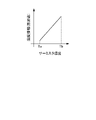
- FIGS. 9 to 12 are diagrams showing the relationship between temperature information and temperature derating in the second embodiment.
- the horizontal axis of FIGS. 9 to 12 indicates the temperature of the thermistor Rth3.
- the vertical axis of FIG. 9 indicates the resistance value of the thermistor Rth3, and the vertical axis of FIG. 710 indicates the magnitude of input to the - terminal of each comparator (comparators COM1, COM2, COM3).
- the vertical axis of FIG. 11 indicates the output voltage (temperature information) of the voltage conversion circuit 70, and the vertical axis of FIG. ing.
- the resistance value of the thermistor Rth3 decreases as the temperature rises.
- the voltage at the connection node between thermistor Rth3 and resistor R16 increases as the temperature rises. That is, as shown in FIG. 10, the input voltage to the - terminal of each comparator (comparators COM1, COM2, COM3) increases as the temperature rises.
- the comparators COM1, COM2, and COM3 are open. Therefore, the voltage conversion circuit 70 outputs a voltage obtained by dividing the voltage Vcc by the resistors R25 and R26.
- the voltage of the - terminal of the comparator COM1 becomes higher than the voltage of the + terminal, and the output of the comparator COM1 becomes L level (ground level).
- the resistor R22 is grounded, and as shown in FIG. 11, the output voltage (temperature information) of the voltage conversion circuit 70 becomes lower than when the temperature is below the temperature Tc.
- the voltage conversion circuit 70 converts the voltage proportional to temperature (analog voltage) shown in B of FIG. 7 into a stepped voltage as shown in FIG.
- the control circuit 40 receives temperature information obtained by converting the detection result of the detection circuit 150 (temperature detection circuit 53) by the voltage conversion circuit 70, and temperature information obtained by the detection circuit 160 (temperature detection circuit 63). Temperature information obtained by converting the detection result of the voltage conversion circuit 70 is taken.
- control circuit 40 controls the light distribution adjustment circuit 32 based on the higher temperature among the temperature information (detection results) and the signal SA.
- temperature derating is not performed below the temperature Tc. That is, the control circuit 40 turns on the plurality of light emitting elements D1 to DN of the ADB light source 30 based on the signal SA from the lamp ECU 2 regardless of the temperature information (detection result) below the temperature Tc.
- control circuit 40 controls the light distribution adjustment circuit 32 so that the drive current flowing through each light emitting element is reduced (for example, to 80% of that when the temperature is below Tc).
- control circuit 40 controls the light distribution adjustment circuit 32 so that the driving current flowing through each light emitting element becomes smaller (for example, 60% of that when the temperature is Tc or lower).
- control circuit 40 controls the light distribution adjustment circuit 32 so that the drive current flowing through each light emitting element is further reduced (for example, to 40% of that when the temperature is Tc or lower).
- the control circuit 40 controls the light distribution adjustment circuit 32 to perform temperature derating.
- heat generation in the power supply substrate K1 and the LED substrate K2 can be suppressed, and thermal destruction of electronic components can be prevented.
- the driving current flowing through each of the light emitting elements D1 to DN is reduced without changing the number of the light emitting elements D1 to DN to be lit.
- the light distribution adjusting circuit 32 is controlled. As a result, power consumption can be reduced (heat generation can be suppressed) without affecting the light distribution pattern.
- the voltage conversion circuit 70 is arranged on the controller board K3. may be sent to the control circuit 40 of the In this case, noise immunity can be improved.
- the voltage conversion circuit 70 is provided on the controller board K3 as in this embodiment, the detection result of the temperature detection circuit 53 and the detection result of the temperature detection circuit 63 can be used in common. Space saving can be achieved.
- FIG. 13 is a block diagram showing an example of a system configuration including the vehicle lamp 1001 of the third embodiment.
- the system shown in FIG. 13 includes a vehicle ECU (Electronic Control Unit) 1010 provided on the vehicle side and a vehicle lamp 1001 on the lamp side.
- a vehicle ECU Electronic Control Unit
- the vehicle ECU 1010 is connected to the lighting ECU 1002 of the vehicle lighting 1001 on the lamp side via a control line such as a CAN (Controller Area Network), and controls the vehicle lighting 1001 in an integrated manner.
- the vehicle ECU 1010 of this embodiment receives vehicle information from the driver's seat of the vehicle and camera information from the vehicle-mounted camera, and based on the information, sends a signal for controlling the vehicle lamp 1001 to the lamp ECU 1002 .
- the vehicle lamp 1001 is, for example, a headlamp provided at the front end of the vehicle.
- the vehicle lamp 1001 is provided on the right side and the left side of the vehicle, respectively, but since the left and right sides have the same configuration, FIG. 13 shows the configuration of only one side (for example, the right side).
- a vehicle lamp 1001 of this embodiment includes a lamp ECU 1002 , a Lo light source 1003 , a Hi light source 1004 and an ADB unit 1005 .
- the lamp ECU 1002 is a device that controls lighting of each light source of the vehicle lamp 1001 .
- a signal including vehicle information, camera information, and the like is input from the vehicle ECU 1010 to the lamp ECU 1002 .
- the lamp ECU 1002 Based on this signal, the lamp ECU 1002 appropriately lights the Lo light source 1003, the Hi light source 1004, and the ADB light source 1030 (described later) of the ADB unit 1005.
- the lamp ECU 1002 transmits a signal SA indicating lighting conditions (light distribution pattern, etc.) of the ADB light source 1030 to the control circuit 1040 (described later) of the ADB unit 1005 .
- This signal SA corresponds to a "second signal".
- the lamp ECU 1002 is supplied with a power supply line with a power supply voltage Vbat from a vehicle battery (battery 1006 shown in FIG. 14) and a ground line with a ground level voltage.
- the lamp ECU 1002 supplies power to the Lo light source 1003 , the Hi light source 1004 and the ADB unit 1005 .
- the Lo light source 1003 is a low beam light source.
- the low beam illuminates the vicinity of the vehicle with a predetermined illuminance, and is used mainly when driving in an urban area.
- a Hi light source 1004 is a high beam light source.
- the high beam illuminates a wide and distant area in front of the vehicle with relatively high illuminance, and is mainly used for high-speed driving on roads with few oncoming and preceding vehicles.
- the ADB unit 1005 is a unit that constitutes a variable light distribution headlamp (ADB: Adaptive Driving Beam) that variably controls the light distribution of the light distribution pattern.
- ADB uses an in-vehicle camera to detect the presence of preceding vehicles, oncoming vehicles, and pedestrians in front of the vehicle. is intended to reduce
- FIG. 14 is a diagram showing a configuration example of the ADB unit 1005.
- FIG. 15 is a diagram showing the configuration of the detection circuit 1050 (and power supply circuit 1020) and the like in the third embodiment.
- the ADB unit 1005 of this embodiment includes a power board K1001, an LED board K2, and a controller board K1003.
- a power supply circuit 1020 and a detection circuit 1050 are arranged on the power supply board K1001, an ADB light source 1030 is arranged on the LED board K2, and a control circuit 1040 is arranged on the controller board K1003.
- each substrate is connected by a signal line such as a harness.
- the ADB light source 1030 is a light source powered by an output voltage (predetermined voltage) of a power supply circuit 1020 described later, and corresponds to a "light source”.
- the ADB light source 1030 includes a plurality (N) of light emitting elements D1001 to D100N, a plurality (N) of current sources 31_1001 to 31_100N, and a light distribution adjustment circuit 1032.
- the plurality of light emitting elements D1001 to D100N and the plurality of current sources 31_1001 to 31_100N are connected in series between the power line and the ground line, respectively. That is, in the ADB light source 1030, a plurality of combinations of series-connected light-emitting elements and current sources are arranged in parallel (connected in parallel).
- the light-emitting elements D1001 to D100N are elements that are turned on by being supplied with a drive current, and LEDs (light-emitting diodes) are used in this embodiment.
- the plurality of light emitting elements D1001 to D100N are connected in parallel and arranged side by side in an array, for example, so as to form a light distribution pattern.
- the current sources 31_1001 to 31_100N supply drive currents to the corresponding light emitting elements.
- the light distribution adjustment circuit 1032 controls the current sources 31_1001 to 31_100N according to the instruction from the control circuit 1040 (signal SC input from the control circuit 1040), and adjusts the drive current flowing through the plurality of light emitting elements D1001 to D100N. . Thereby, lighting can be performed with a light distribution pattern according to the situation of the vehicle. Note that the light distribution adjustment circuit 1032 corresponds to an "adjustment unit".
- a method for adjusting the drive current by the light distribution adjustment circuit 1032 is not particularly limited, and for example, PWM control or analog control can be applied.
- the current sources 31_1001 to 31_100N are configured by current mirror circuits, and by adjusting the magnitude of the drive current flowing through one light emitting element, the magnitude of the dynamic current flowing through the other light emitting elements can be adjusted accordingly. I am trying to change.
- Control circuit 1040 outputs a signal SC indicating collectively turning on/off the plurality of light emitting elements D1001 to D100N, brightness patterns, etc., based on the signal SA from the lamp ECU 1002 (and the signal SB from the detection circuit 1050, which will be described later). It generates and outputs to the ADB light source 1030 (light distribution adjustment circuit 1032). Thereby, the control circuit 1040 controls the light distribution adjustment circuit 1032 to light the plurality of light emitting elements D1001 to D100N with desired brightness. Note that the control circuit 1040 corresponds to a "control section".
- a plurality of light emitting elements D1001 to D100N are connected in parallel.
- the larger the number of light-emitting elements to be lit the larger the current required.
- the number of light emitting elements is 1000 and the current required for lighting each element is 10 mA
- a total current supply capacity of 10 A is required.
- the detection circuit 1050 is provided on the power supply board K1001 on which the power supply circuit 1020 is arranged. Based on the signal SB output from the detection circuit 1050 and the signal SA indicating the lighting condition from the lamp ECU 1002, temperature derating is performed to reduce the power consumption according to the temperature rise.
- the power supply circuit 1020 is a voltage regulator that generates a predetermined voltage (eg 5V) based on the power supply voltage Vbat (eg 12V) supplied from the battery 1006 of the vehicle.
- the power supply circuit 1020 of this embodiment is a step-down DC-DC converter (eg, switching regulator).
- a linear regulator may be used, or a configuration including a booster circuit and a step-down circuit (a configuration in which the voltage is stepped up after being stepped up) may be used.
- the power supply circuit 1020 is a so-called synchronous rectification type circuit, and as shown in FIG. there is
- the capacitor C1001 is an input-side capacitor, one end of which is connected to the power supply line and the other end of which is connected (grounded) to the ground line.
- the transistors M1001 and M1002 are NMOSFETs, the drain of the transistor M1001 is connected to one end of the capacitor C1001, and the source of the transistor M1001 is connected to the drain of the transistor M1002 and one end of the coil L1001.
- the source of transistor M1002 is grounded.
- Gates of the transistors M1001 and M1002 are connected to the control IC 1021, and the transistors M1001 and M1002 are controlled to be turned on/off by the control IC1021.
- the other end of the coil L1001 is connected to one end of the output-side capacitor C1002 via a resistor R1001. Also, the other end of the capacitor C1002 is grounded. The voltage generated across the capacitor C1002 is the output voltage.
- the resistors R1002 and R1003 are connected in series between the connection point between the resistor R1001 and one end of the capacitor C1002 and the ground. Also, the voltage at the connection point between the resistors R1002 and R1003 (the voltage obtained by dividing the output voltage by the resistors R1002 and R1003) is taken into the control IC 1021 .
- the control IC 1021 switches the transistors M1001 and M1002 based on the voltage generated at the connection point between the resistors R1002 and R1003 so that the output voltage of the power supply circuit 1020 becomes a predetermined voltage.
- the input voltage (the voltage of the capacitor C1001) is applied to one end of the coil L1001.
- the ground line voltage (ground voltage) is applied to one end of the coil L1001.
- the output voltage of the power supply circuit 1020 becomes lower than the input voltage (power supply voltage Vbat) and is controlled to a predetermined voltage (eg, 5V).
- the detection circuit 1050 is provided on the power supply board K1001 on which the power supply circuit 1020 is arranged, and has a temperature detection circuit 1051 and an interface circuit (hereinafter referred to as I/F circuit) 1052 .
- the temperature detection circuit 1051 is a circuit that is provided on the power supply board K1001 and detects temperature.
- the temperature detection circuit 1051 of this embodiment is composed of an oscillation circuit that outputs a signal SD having a frequency corresponding to temperature.
- the temperature detection circuit 1051 includes resistors R1004 to R1006, capacitors C1003 and C1004, a thermistor Rth1001, and an operational amplifier OP1001.
- the resistors R1004 and R1005 are connected in series, one end (one end of the resistor R1004) is applied with the voltage Vcc, and the other end (the other end of the resistor R1005) is grounded.
- One end of the capacitor C1003 is connected to the connection point between the series-connected resistors R1004 and R1005, and the other end is grounded.
- the inverting input terminal (-terminal) of the operational amplifier OP1001 is grounded via a capacitor C1004 and connected to the output of the operational amplifier OP1001 via a thermistor Rth1001.
- the thermistor Rth1001 is an electronic component whose resistance value changes according to changes in temperature (see FIG. 16).
- non-inverting input terminal (+ terminal) of the operational amplifier OP1001 is connected to the connection point between the resistors R1004 and R1005, and is also connected to the output of the operational amplifier OP1001 via the resistor R1006.
- This temperature detection circuit 1051 is obtained by replacing part of the resistance (the resistance connected between the - terminal and the output) with a thermistor Rth1001 in the oscillation circuit using the operational amplifier OP1001. As the resistance value of the thermistor Rth1001 changes according to the temperature, the frequency of the output signal (signal SD) changes. This signal SD corresponds to the "first signal”.
- the temperature detection circuit 1051 may output a signal SD having a frequency corresponding to the resistance value of the thermistor Rth 1001. For example, a Hartley oscillation circuit or a Wien bridge oscillation circuit may be used.
- the I/F circuit 1052 is a circuit that converts the signal SD output from the temperature detection circuit 1051 into a logic level signal (signal SB).
- a logic level signal is a square-wave signal that switches between a high level (H level hereinafter) and a low level (L level hereinafter).
- the I/F circuit 1052 includes a transistor M1003, resistors R1007 to R1009, a coil L1002, and a capacitor C1005. Also, the coil L1002 and the capacitor C1005 are connected to a pull-up resistor (not shown) inside the control circuit 1040 .
- the transistor M1003 is an NPN transistor whose emitter is grounded and whose collector is connected to one end of the coil L1002 via a resistor R1009. Power is supplied from the control circuit 1040, for example, to the collector of the NPN transistor M1003.
- the base of the NPN transistor M1003 is connected to the connection point between the resistors R1007 and R1008 connected in series between the output of the temperature detection circuit 1051 (the output of the operational amplifier OP1001) and the ground. That is, the voltage obtained by dividing the output (signal SD) of the temperature detection circuit 1051 by the resistors R1007 and R1008 is applied to the base of the NPN transistor M1003.
- One end of the capacitor C1005 is connected to the other end of the coil L1002, and the other end of the capacitor C1005 is grounded. Note that the coil L1002 and the capacitor C1005 constitute a filter for removing noise. Also, the voltage across the capacitor C1005 is the output of the detection circuit 1050 .
- an L level signal is output when the NPN transistor M1003 is turned on, and an H level signal is output when the NPN transistor M1003 is turned off.
- the output (signal SB) of the I/F circuit 1052 becomes a rectangular wave signal (logical level signal) indicating temperature information based on the signal SD (oscillation signal).
- the signal SB is a rectangular wave, making it less susceptible to noise (increasing noise resistance).
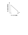
- FIGS. 16 to 18 are diagrams for explaining the relationship between the temperature information of the temperature detection circuit 1051 and the temperature derating.
- the horizontal axis of FIGS. 16 to 18 indicates the temperature of the thermistor Rth1001.
- the vertical axis in FIG. 16 represents the resistance value of the thermistor Rth 1001, the vertical axis in FIG. It shows the magnitude of the output current (driving current flowing through the light emitting element) in the light source 1030 .
- the resistance value of the thermistor Rth1001 decreases as the temperature rises.
- the frequency of oscillation of signal SD increases as the temperature of the thermistor rises.
- the control circuit 1040 controls the temperature as shown in FIG. Accordingly, it generates a signal SC that reduces the power consumption (driving current flowing through the light emitting element) and controls the light distribution adjustment circuit 1032 (performs temperature derating). By doing so, it is possible to suppress heat generation and prevent destruction of electronic components.
- the temperature information (frequency) range (range corresponding to temperatures Ta to Tb) for temperature derating is designed in accordance with the specifications of control circuit 1040, which is the information receiving side.
- control circuit 1040 performs temperature derating so that the drive current flowing through each of the light emitting elements D1001 to D100N is reduced without changing the number of the light emitting elements D1001 to D100N to be lit. , controls the light distribution adjustment circuit 1032 . As a result, power consumption can be reduced (heat generation can be suppressed) without affecting the light distribution pattern.
- the present invention is not limited to this, and for example, the upper limit of the drive current flowing through each light emitting element may be lowered, or the light distribution pattern may be changed.
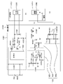
- FIG. 19 is a diagram showing the configuration of the detection circuit 1150 in the fourth embodiment.
- parts having the same configurations as in FIG. 15 are denoted by the same reference numerals, and description thereof is omitted.
- a power supply circuit 1020 and a detection circuit 1150 are provided on the power supply board K1001.
- the detection circuit 1150 has a temperature detection circuit 1051 , an I/F circuit 1052 and a signal output circuit 1053 .
- the signal output circuit 1053 is a circuit that outputs a signal SE that serves as a trigger when temperature derating is performed separately from the temperature detection circuit 1051, and includes resistors R1010 to R1012, a thermistor Rth1002, and a comparator COM1001. It is configured. Note that the signal output circuit 1053 corresponds to the "output circuit”, and the signal SE corresponds to the "third signal”.
- the resistor R1010 and the resistor R1011 are connected in series, and the voltage Vcc is applied to one end (the end of the resistor R1010) and the other end (the end of the resistor R1011) is grounded.
- the thermistor Rth1002 and the resistor R1012 are also connected in series, one end (the end of the thermistor Rth1002) is applied with the voltage Vcc, and the other end (the end of the resistor R1012) is grounded.
- the inverting input terminal (- terminal) of the comparator COM1001 is connected to the connection point between the resistors R1010 and R1011, and the non-inverting input terminal (+ terminal) is connected to the connection point between the thermistor Rth1002 and the resistor R1012. Then, the comparator COM1001 compares the voltage of the + terminal and the voltage of the - terminal, and outputs the comparison result.
- the comparator COM1001 of this embodiment is an open-drain type, and outputs an open (high impedance) voltage when the voltage of the + terminal is higher than the voltage of the - terminal, and outputs an L level (ground level) voltage when the voltage is lower than that of the - terminal.
- the resistance values of the resistors R1010, R1011, and R1012 are set so that the output of the comparator COM1001 switches at the temperature Ta shown in FIGS.
- the resistance of the thermistor Rth1002 is small, so the voltage of the + terminal of the comparator COM1001 becomes higher than the voltage of the - terminal. As a result, the output of the comparator COM1001 becomes open.
- the resistance of the thermistor Rth1002 increases, and the voltage at the - terminal of the comparator COM1001 becomes higher than the voltage at the + terminal. As a result, the output of the comparator COM1001 becomes L level.
- the output of this comparator COM1001 is output to the control circuit 1040 as a signal SE.
- the predetermined temperature Ta corresponds to the "second temperature”.
- the control circuit 1040 of the fourth embodiment takes in the output signal (signal SE) of the signal output circuit 1053 in addition to the signal SB. Then, the control circuit 1040 does not perform temperature derating when the signal SE becomes L level. That is, regardless of the output signal SB of the I/F circuit 1052 (in other words, the output signal SD of the temperature detection circuit 1051), the plurality of light emitting elements D1001 to D100N are lit based on the signal SA from the lamp ECU 1002. .
- the output of the signal output circuit 1053 (signal SE) can be used as a trigger to stop temperature derating.
- the signal output circuit 1053 detects the lower limit (temperature Ta) of the range requiring temperature derating, but a circuit for detecting the upper limit (temperature Tb) may also be provided. As a result, temperature derating can be reliably performed in the temperature range where temperature derating is required.
- FIG. 20 is a diagram showing the configuration of the detection circuit 1250 in the fifth embodiment.
- parts having the same configurations as those in FIGS. 15 and 19 are denoted by the same reference numerals, and descriptions thereof are omitted.
- a power supply circuit 1020 and a detection circuit 1250 are provided on the power supply board K1001.
- the detection circuit 1250 has a temperature detection circuit 1051 , an I/F circuit 1052 and an oscillation stop circuit 1054 .
- the oscillation stop circuit 1054 includes resistors R1013 to R1015, a thermistor Rth1003, and a comparator COM1002. As shown in FIG. 20, the oscillation stop circuit 1054 has the same configuration as the signal output circuit 1053 of the fourth embodiment (FIG. 19), so description thereof will be omitted.
- the output of the oscillation stop circuit 1054 (the output of the comparator COM1002) is connected to the connection point between the ⁇ terminal of the operational amplifier OP1001 of the temperature detection circuit 1051, the thermistor Rth1001, and the capacitor C1004. Note that the oscillation stop circuit 1054 corresponds to a "stop circuit".
- the temperature detection circuit 1051 performs an oscillation operation (temperature detection) according to the temperature, and temperature derating is performed based on the result.
- the resistance of the thermistor Rth1003 increases, and the voltage of the - terminal of the comparator COM1002 becomes higher than the voltage of the + terminal.
- the output of the comparator COM1002 becomes L level.
- the ⁇ terminal of the operational amplifier OP1001 becomes the ground level, and the operational amplifier OP1001 stops oscillating (oscillating operation is forcibly stopped).
- the oscillation stop circuit 1054 stops the operation of the temperature detection circuit 1051 when the temperature drops below the temperature Ta.
- no temperature derating is performed. Note that the temperature Ta at this time corresponds to the "first temperature”.
- the temperature derating can be stopped by using the output of the oscillation stop circuit 1054 as a trigger.
- FIG. 21 is a diagram showing the configuration of the detection circuit 1350 in the sixth embodiment.
- parts having the same configurations as those in FIGS. 15, 19, and 20 are denoted by the same reference numerals, and descriptions thereof are omitted.
- a power supply circuit 1020 and a detection circuit 1350 are provided on the power supply board K1001.
- the detection circuit 1350 has a temperature detection circuit 55 and a buffer circuit 56 .
- the temperature detection circuit 55 includes resistors R1016 to R1025, comparators COM1003 to COM1005, and a thermistor Rth1004.
- the resistors R1016 to R1019 are connected in series, and the voltage Vcc is applied to one end (the end of the resistor R1016) and the other end (the end of the resistor R1019) is grounded.
- the thermistor Rth1004 and the resistor R1020 are connected in series and provided in parallel with the resistors R1016 to R1019. That is, the voltage Vcc is applied to one end of the thermistor Rth1004 and the resistor R1020 connected in series (the end of the thermistor Rth1004), and the other end (the end of the resistor R1020) is grounded.
- the resistors R1024 and R1025 are connected in series, one end of which is applied with the voltage Vcc (the end of the resistor R1024) and the other end (the end of the resistor R1025) is grounded.
- the voltage at the connection point between the thermistor Rth1004 and the resistor R1020 is applied to the inverting input terminal ( ⁇ terminal) of the comparator COM1003, and the voltage at the connection point between the resistors R1018 and R1019 is applied to the non-inverting input terminal (+ terminal). applied. Also, the output of the comparator COM1003 is connected to the connection point of the resistors R1024 and R1025 via the resistor R1021.
- the voltage at the connection point between the thermistor Rth1004 and the resistor R1020 is applied to the - terminal of the comparator COM1004, and the voltage at the connection point between the resistors R1017 and R1018 is applied to the + terminal. Also, the output of the comparator COM1003 is connected to the connection point of the resistors R1024 and R1025 via the resistor R1022.
- the voltage at the connection point between the thermistor Rth1004 and the resistor R1020 is applied to the - terminal of the comparator COM1005, and the voltage at the connection point between the resistors R1016 and R1017 is applied to the + terminal. Also, the output of the comparator COM1003 is connected to the connection point of the resistors R1024 and R1025 via the resistor R1023.
- the comparators COM1003, COM1004, and COM1005 are open-drain comparators, and are open (high impedance) when the + terminal voltage is higher than the - terminal voltage, and the + terminal voltage is higher than the - terminal voltage. If it is smaller, it outputs an L level (ground level) voltage.
- the buffer circuit 56 is a circuit that prevents the output voltage from fluctuating according to the input impedance, and is composed of an operational amplifier OP1002 (voltage follower) whose output is negatively fed back.
- the output voltage of the temperature detection circuit 55 (the voltage at the connection node of the resistors R1024 and R1025) is applied to the + terminal of the operational amplifier OP1002, and the output of the operational amplifier OP1002 is sent to the control circuit 1040 as the signal SB.
- FIGS. 22 to 25 are diagrams showing the relationship between the temperature information of the temperature detection circuit 55 and the temperature derating.
- the horizontal axis of FIGS. 22 to 25 indicates the temperature of the thermistor Rth1004.
- the vertical axis of FIG. 22 indicates the resistance value of the thermistor Rth1004, and the vertical axis of FIG. 23 indicates the magnitude of input to the - terminal of each comparator (comparators COM1003, COM1004, COM1005).
- the vertical axis in FIG. 24 indicates the output (signal SB) of the detection circuit 1350, and the vertical axis in FIG. 25 indicates the magnitude of the output current (driving current flowing through each light emitting element) in the ADB light source 1030. .
- the resistance value of the thermistor Rth1004 decreases as the temperature rises.
- the input voltage to the - terminal of each comparator increases as the thermistor temperature rises.
- This input voltage corresponds to a "first voltage” according to temperature
- the thermistor Rth1004 and resistor R1020 correspond to a "voltage generation circuit” that generates the input voltage (first voltage).
- the comparators COM1003, COM1004, and COM1005 are open. Therefore, a voltage obtained by dividing the voltage Vcc by the resistors R1024 and R1025 is output as the signal SB.
- the control circuit 1040 does not perform temperature derating below this temperature Tc. That is, in the present embodiment, the temperature Tc corresponds to the “second temperature”, and the control circuit 1040 controls the temperature of the ADB light source 1030 based on the signal SA from the lamp ECU 1002 regardless of the signal SB below the temperature Tc.
- the light emitting elements D1001 to D100N are turned on.
- the control circuit 1040 performs temperature derating by controlling the light distribution adjustment circuit 1032 so that the drive current flowing through each light emitting element is reduced (for example, to 80% when the temperature is equal to or lower than the temperature Tc).
- the control circuit 1040 performs temperature derating by controlling the light distribution adjustment circuit 1032 so that the driving current flowing through each light emitting element becomes smaller (for example, 60% when the temperature is equal to or lower than Tc).
- the control circuit 1040 performs temperature derating by controlling the light distribution adjustment circuit 1032 so that the drive current flowing through each light emitting element is further reduced (for example, to 40% when the temperature is equal to or lower than Tc).
- the voltage (the input voltage of the - terminal of each comparator) that changes according to the temperature rise of the thermistor is converted into a stepped voltage as shown in FIG.
- This stepwise voltage corresponds to the "second voltage”
- the portion of the temperature detection circuit 55 other than the thermistor Rth1004 and the resistor R1020 corresponds to the "voltage conversion circuit”.
- a vehicle lamp 1 is a lamp used in a vehicle, and includes a power supply circuit 20 provided on a power supply board K1 for generating a predetermined voltage based on a power supply voltage Vbat, an ADB light source 30 provided on an LED board K2, and a controller.
- a control circuit 40 is provided on the substrate K3.
- the ADB light source 30 is a light source using a predetermined voltage as a power supply, and includes a plurality of light emitting elements D1 to DN and a light distribution adjustment circuit 32 that adjusts the drive current flowing through each of the plurality of light emitting elements D1 to DN.
- the power supply board K1 of the first embodiment is provided with a temperature detection circuit 51 for detecting temperature
- the LED board K2 is provided with a temperature detection circuit 61 for detecting temperature.
- the light distribution adjustment circuit 32 is controlled based on the detection result of the higher temperature among the detection results of the detection circuits 51 and 61 and the signal SA indicating the lighting conditions of the plurality of light emitting elements D1 to DN. .
- heat generation in the power supply board K1 and the LED board K2 can be efficiently suppressed, and destruction of electronic components can be prevented.
- the temperature detection circuits 51 and 61 are oscillation circuits that oscillate at frequencies corresponding to temperature. As a result, the temperatures of the power board K1 and the LED board K2 can be detected from the respective frequencies.
- the power supply board K1 is provided with an I/F circuit 52 for converting the output signal SD1 of the temperature detection circuit 51 into a logic level signal SB1, and the LED board K2 is provided with the output signal SD2 of the temperature detection circuit 61. , is provided with an I/F circuit 62 for converting into a logic level signal SB2. This makes it possible to reduce the influence of noise (improve noise immunity).
- the power supply board K1 is provided with the temperature detection circuit 53 including the resistor R16 and the thermistor Rth3, and the LED board K2 is provided with the temperature detection circuit 63 including the resistor R17 and the thermistor Rth4.
- the temperature detection circuit 53 including the resistor R16 and the thermistor Rth3
- the LED board K2 is provided with the temperature detection circuit 63 including the resistor R17 and the thermistor Rth4.
- It also has a voltage conversion circuit 70 that converts the detection result of the temperature detection circuit 53 and the detection result of the temperature detection circuit 63 into a stepped voltage waveform. Thereby, noise tolerance can be improved.
- the voltage conversion circuit 70 is provided on the controller board K3. As a result, the detection result of the temperature detection circuit 53 and the detection result of the temperature detection circuit 63 can be converted by the single voltage conversion circuit 70, so that the number of components can be reduced and the space can be saved.
- control circuit 40 controls the number of the light emitting elements D1 to DN to be lit without changing the number of the light emitting elements D1 to DN to be turned on, so that the driving current flowing through each of the plurality of light emitting elements D1 to DN becomes small. Control the coordinator. As a result, power consumption can be reduced without affecting the light distribution pattern.
- the lamp (vehicle lamp 1) of the present embodiment can be suitably used as a vehicle headlamp (especially ADB).
- vehicle headlamp especially ADB
- the vehicle lamp 1001 of the third to sixth embodiments has been described.
- the vehicle lamp 1001 is a lamp used in a vehicle, and the power supply circuit 1020 generates a predetermined voltage obtained by stepping down the power supply voltage Vbat, the plurality of light emitting elements D1001 to D100N, and the plurality of light emitting elements D1001 to D100N. and a light distribution adjustment circuit 1032 for adjusting the drive current, and an ADB light source 1030 powered by a predetermined voltage.
- a temperature detection circuit 1051 is provided on the power supply board K1001 on which the power supply circuit 1020 is arranged. and a control circuit 1040 that controls the light distribution adjustment circuit 1032 based on a signal SA indicating the lighting condition.
- the temperature detection circuit 1051 of the third to fifth embodiments is an oscillation circuit that outputs a signal SD having a frequency corresponding to temperature by using the thermistor Rth1001 whose resistance changes with temperature. Thereby, the temperature can be detected from the oscillation frequency.
- the third to fifth embodiments include an I/F circuit 1052 that converts the signal SD into a logic level signal SB.
- I/F circuit 1052 that converts the signal SD into a logic level signal SB.
- the power supply board K1001 has an oscillation stop circuit 1054 that stops the operation of the temperature detection circuit 1051 when the temperature drops below the temperature Ta. Thereby, it is possible to improve the accuracy of the temperature when performing the temperature derating.
- the temperature detection circuit 55 of the sixth embodiment includes a voltage generation circuit (thermistor Rth1004 and resistor R1020) that generates a voltage corresponding to temperature, and a voltage that converts the voltage into a stepped voltage and outputs it as a signal SB. It includes a conversion circuit (a portion of the temperature detection circuit 55 excluding the thermistor Rth1004 and the resistor R1020). Thereby, when the signal SB is transmitted to the control circuit 1040, noise immunity can be improved.
- a voltage generation circuit thermoistor Rth1004 and resistor R1020
- control circuit 1040 of the third to fifth embodiments when the detected temperature is equal to or lower than the temperature Ta (temperature Tc in the sixth embodiment), controls the plurality of The light emitting elements D1001 to D100N are turned on. As a result, it is possible not to perform temperature derating in a temperature range where temperature derating is unnecessary.
- a signal output circuit 53 is provided for outputting to the control circuit 1040 a signal SE indicating that the temperature has become equal to or lower than Ta. As a result, it is possible to improve the accuracy of the temperature at which temperature derating is performed.
- control circuit 1040 controls the number of light emitting elements D1001 to D100N to be lit without changing the number of light emitting elements D1001 to D100N so that the drive current flowing through each of the plurality of light emitting elements D1001 to D100N is reduced. Control the coordinator. As a result, power consumption can be reduced without affecting the light distribution pattern.
- the lamp (vehicle lamp 1001) of the present embodiment can be suitably used as a vehicle headlamp (especially ADB).
- vehicle headlamp especially ADB
- control circuit 40 and the light distribution adjustment circuit 32 are provided separately in the above embodiment, for example, a part of the microcomputer may be configured to function as the control section and the adjustment section.
- the detection results of the temperature detection circuits 51 and 61 are converted into stepped voltages by the voltage conversion circuit 70. 40 may be incorporated. Then, temperature derating may be performed based on one of the detection results (the one with the higher temperature) and the signal SA.
- each circuit of the ADB unit 1005 was configured on three boards (power supply board K1001, LED board K2, controller board K1003), but may be configured on one board.
- control circuit 1040 and the light distribution adjustment circuit 1032 may be configured by, for example, part of a microcomputer functioning as a control unit and an adjustment unit.
- Vehicle ECU 20 power supply circuit 21 control IC 30 ADB light sources 31_1 to 31_N current source 32 light distribution adjustment circuit 40 control circuits 50, 60 detection circuits 51, 61 temperature detection circuits 52, 62 interface circuits 53, 63 temperature detection circuits 54, 64, 71 buffer circuit 70 voltage conversion circuit 150 , 160 detection circuits C1 to C8 capacitors COM1 to COM3 comparators D1 to DN light emitting elements, K1 Power supply board K2 LED board K3 Controller board L1-L3 Coils M1-M4 Transistors OP1-OP5 Operational amplifiers R1-R26 Resistors Rth1-Rth4 Thermistors SA, SB, SB1, SB2, SC, SD, SD1, SD2, SE1, SE2 Signal SW1 switch Vbat power supply voltage Vcc voltage 1001 vehicle lamp 1002 lamp ECU 1003 Lo light source 1004 Hi light source 1005 ADB unit 1006 Battery 1010 Vehicle ECU
Landscapes
- Engineering & Computer Science (AREA)
- General Engineering & Computer Science (AREA)
- Physics & Mathematics (AREA)
- Microelectronics & Electronic Packaging (AREA)
- Optics & Photonics (AREA)
- Lighting Device Outwards From Vehicle And Optical Signal (AREA)
Abstract
Description
図1に示すシステムは、車両側に設けられた車両ECU(Electronic Control Unit)10と、ランプ側の車両用灯具1を含む。 =====First Embodiment=====
The system shown in FIG. 1 includes a vehicle ECU (Electronic Control Unit) 10 provided on the vehicle side and a
図2は、第1実施形態におけるADBユニット5の構成を示すブロック図である。また、図3は、図2に示す電源基板K1に配置された回路の構成例を示す図であり、図4は、図2に示すLED基板K2に配置された回路の構成例を示す図である。 <<Configuration of
FIG. 2 is a block diagram showing the configuration of the
電源回路20は、車両のバッテリー6から供給される電源電圧Vbat(例えば12V)に基づいて、所定電圧(例えば5V)を生成する電圧レギュレータである。本実施形態の電源回路20は、降圧型のDC-DCコンバータ(例えば、スイッチングレギュレータ)である。ただし、これには限られず、例えば、リニアレギュレータでもよいし、昇圧回路と降圧回路を含む構成(昇圧した後に降圧する構成)であってもよい。 <
The
ADB光源30は、電源回路20の出力電圧(所定電圧)を電源とする光源であり、「光源」に相当する。 <ADB
The ADB
制御回路40は、灯具ECU2からの信号SA(及び、後述する検出回路50,60からの信号SB1,SB2)に基づいて、複数の発光素子D1~DNの点消灯、輝度パターンなどを一括指示する信号SCを生成してADB光源30の配光調整回路32に出力する。これにより、制御回路40は、配光調整回路32を制御し、複数の発光素子D1~DNを、それぞれ、所望の明るさで点灯させる。なお、制御回路40は、「制御部」に相当する。 <
Based on a signal SA from the lamp ECU 2 (and signals SB1 and SB2 from
検出回路50は、電源回路20が配置された電源基板K1に設けられており、温度検出回路51と、インターフェース回路(以下、I/F回路)52とを有する。 <
The
検出回路60は、ADB光源30が配置されたLED基板K2に設けられており、温度検出回路61と、I/F回路62とを有する。 <
The
制御回路40は、検出回路50(換言すると温度検出回路51)の検出結果及び検出回路60(換言すると温度検出回路61)の検出結果のうちの一方と、灯具ECU2からの配光パターン(点灯条件)を示す信号SAとに基づいて温度ディレーティングを行う。 <<About temperature derating>>
The
第2実施形態ではADBユニットの構成が、第1実施形態と異なる。
図8は、第2実施形態のADBユニット15の構成を示す図である。図8において、第1実施形態と同一構成の部分には同一符号を付し説明を省略する。 ===== Second Embodiment =====
The configuration of the ADB unit in the second embodiment differs from that in the first embodiment.
FIG. 8 is a diagram showing the configuration of the
<<<システム構成>>>
図13は、第3実施形態の車両用灯具1001を含むシステム構成の一例を示すブロック図である。 ===== Third Embodiment =====
<<<system configuration>>>
FIG. 13 is a block diagram showing an example of a system configuration including the
図14は、ADBユニット1005の構成例を示す図である。また、図15は、第3実施形態における検出回路1050(及び電源回路1020)等の構成を示す図である。 <<Configuration of
FIG. 14 is a diagram showing a configuration example of the
ADB光源1030は、後述する電源回路1020の出力電圧(所定電圧)を電源とする光源であり、「光源」に相当する。 <ADB
The
制御回路1040は、灯具ECU1002からの信号SA(及び、後述する検出回路1050からの信号SB)に基づいて、複数の発光素子D1001~D100Nの点消灯、輝度パターンなどを一括指示する示す信号SCを生成してADB光源1030(配光調整回路1032)に出力する。これにより、制御回路1040は、配光調整回路1032を制御し、複数の発光素子D1001~D100Nを、それぞれ、所望の明るさで点灯させる。なお、制御回路1040は、「制御部」に相当する。 <
The
電源回路1020は、車両のバッテリー1006から供給される電源電圧Vbat(例えば12V)に基づいて、所定電圧(例えば5V)を生成する電圧レギュレータである。本実施形態の電源回路1020は、降圧型のDC-DCコンバータ(例えば、スイッチングレギュレータ)である。ただし、これには限られず、例えば、リニアレギュレータでもよいし、昇圧回路と降圧回路を含む構成(昇圧した後に降圧する構成)であってもよい。 <
The
検出回路1050は、電源回路1020が配置された電源基板K1001に設けられており、温度検出回路1051と、インターフェース回路(以下、I/F回路)1052とを有する。 <
The
図19は、第4実施形態における検出回路1150の構成を示す図である。図19において、図15と同一構成の部分には同一符号を付し、説明を省略する。第4実施形態では電源基板K1001上に、電源回路1020と、検出回路1150が設けられている。 ===== Fourth Embodiment =====
FIG. 19 is a diagram showing the configuration of the
図20は、第5実施形態における検出回路1250の構成を示す図である。図20において、図15、図19と同一構成の部分には同一符号を付し、説明を省略する。第5実施形態では電源基板K1001上に、電源回路1020と、検出回路1250が設けられている。 ===== Fifth Embodiment =====
FIG. 20 is a diagram showing the configuration of the
図21は、第6実施形態における検出回路1350の構成を示す図である。図21において、図15,図19,図20と同一構成の部分には同一符号を付し、説明を省略する。第6実施形態では電源基板K1001上に、電源回路1020と、検出回路1350が設けられている。 =====Sixth Embodiment=====
FIG. 21 is a diagram showing the configuration of the
以上、第1実施形態および第2実施形態の車両用灯具1について説明した。車両用灯具1は、車両に用いられる灯具であり、電源基板K1に設けられ、電源電圧Vbatに基づいて所定電圧を生成する電源回路20と、LED基板K2に設けられたADB光源30と、コントローラ基板K3に設けられた制御回路40を備えている。ADB光源30は、所定電圧を電源とする光源であり、複数の発光素子D1~DNと、複数の発光素子D1~DNのそれぞれに流れる駆動電流を調整する配光調整回路32と、を含む。また、第1実施形態の電源基板K1には、温度を検出する温度検出回路51が設けられ、LED基板K2には温度を検出する温度検出回路61が設けられており、制御回路40は、温度検出回路51,61のそれぞれの検出結果のうちの温度の高い方の検出結果と、複数の発光素子D1~DNの点灯条件を示す信号SAと、に基づいて、配光調整回路32を制御する。これにより、電源基板K1及びLED基板K2における発熱を効率的に抑制することができ、電子部品の破壊を防ぐことが可能である。 ===Summary===
The
2 灯具ECU
3 Lo光源
4 Hi光源
5,15 ADBユニット
6 バッテリー
10 車両ECU
20 電源回路
21 制御IC
30 ADB光源
31_1~31_N 電流源
32 配光調整回路
40 制御回路
50,60 検出回路
51,61 温度検出回路
52,62 インターフェース回路
53,63 温度検出回路
54,64,71 バッファ回路
70 電圧変換回路
150,160 検出回路
C1~C8 コンデンサ
COM1~COM3 コンパレータ
D1~DN 発光素子、
K1 電源基板
K2 LED基板
K3 コントローラ基板
L1~L3 コイル
M1~M4 トランジスタ
OP1~OP5 オペアンプ
R1~R26 抵抗
Rth1~Rth4 サーミスタ
SA,SB,SB1,SB2,SC,SD,SD1,SD2,SE1,SE2 信号
SW1 スイッチ
Vbat 電源電圧
Vcc 電圧
1001 車両用灯具
1002 灯具ECU
1003 Lo光源
1004 Hi光源
1005 ADBユニット
1006 バッテリー
1010 車両ECU
1020 電源回路
1021 制御IC
1030 ADB光源
31_1001~31_100N 電流源
1032 配光調整回路
1040 制御回路
1050 検出回路
1051 温度検出回路
1052 インターフェース回路
1053 信号出力回路
1054 発振停止回路
1055 温度検出回路
1056 バッファ回路
1150,1250,1350 検出回路
C1001~C1005 コンデンサ
COM1001~COM1005 コンパレータ
D1001~D100N 発光素子、
K1001 電源基板
K1002 LED基板
K1003 コントローラ基板
L1001,L1002 コイル
M1001,M1002 トランジスタ
M1003 NPNトランジスタ
OP1001,OP1002 オペアンプ
R1001~R1025 抵抗
Rth1001~Rth1004 サーミスタ 1
3 Lo
20
30 ADB light sources 31_1 to 31_N
K1 Power supply board K2 LED board K3 Controller board L1-L3 Coils M1-M4 Transistors OP1-OP5 Operational amplifiers R1-R26 Resistors Rth1-Rth4 Thermistors SA, SB, SB1, SB2, SC, SD, SD1, SD2, SE1, SE2 Signal SW1 switch Vbat power supply
1003
1020
1030 ADB light source 31_1001 to 31_100N
K1001 Power board K1002 LED board K1003 Controller board L1001, L1002 Coils M1001, M1002 Transistor M1003 NPN transistor OP1001, OP1002 Operational amplifier R1001 to R1025 Resistor Rth1001 to Rth1004 Thermistor
Claims (17)
- 第1基板に設けられ、電源電圧に基づいて所定電圧を生成する電源回路と、
第2基板に設けられ、複数の発光素子と、前記複数の発光素子のそれぞれに流れる駆動電流を調整する調整部と、を含み、前記所定電圧を電源とする光源と、
第3基板に設けられ、前記調整部を制御する制御部と、
前記第1基板に設けられ、温度を検出する第1温度検出回路と、
前記第2基板に設けられ、温度を検出する第2温度検出回路と、
を有し、
前記制御部は、前記第1及び第2温度検出回路のそれぞれの検出結果のうちの温度の高い方の検出結果と、前記複数の発光素子の点灯条件を示す信号と、に基づいて、前記調整部を制御する、
灯具。 a power supply circuit provided on the first substrate and configured to generate a predetermined voltage based on the power supply voltage;
a light source provided on a second substrate, including a plurality of light emitting elements and an adjustment unit configured to adjust drive currents flowing through each of the plurality of light emitting elements, the light source being powered by the predetermined voltage;
a control unit provided on a third substrate for controlling the adjustment unit;
a first temperature detection circuit provided on the first substrate for detecting temperature;
a second temperature detection circuit provided on the second substrate for detecting temperature;
has
The control unit performs the adjustment based on the detection result of the higher temperature among the detection results of each of the first and second temperature detection circuits and a signal indicating lighting conditions of the plurality of light emitting elements. control the department,
lamp. - 前記第1及び第2温度検出回路は、それぞれ、温度に応じた周波数で発振する発振回路である、
請求項1に記載の灯具。 Each of the first and second temperature detection circuits is an oscillation circuit that oscillates at a frequency according to temperature,
The lamp according to claim 1. - 前記第1基板には、前記第1温度検出回路の出力信号を、論理レベルの信号に変換する第1インターフェース回路が設けられ、
前記第2基板には、前記第2温度検出回路の出力信号を、論理レベルの信号に変換する第2インターフェース回路が設けられている、
請求項2に記載の灯具。 The first substrate is provided with a first interface circuit that converts the output signal of the first temperature detection circuit into a logic level signal,
The second substrate is provided with a second interface circuit that converts the output signal of the second temperature detection circuit into a logic level signal.
The lamp according to claim 2. - 前記第1及び第2温度検出回路は、それぞれ、抵抗とサーミスタを含んで構成される、
請求項1に記載の灯具。 the first and second temperature detection circuits each comprise a resistor and a thermistor;
The lamp according to claim 1. - 前記第1及び第2温度検出回路のそれぞれの検出結果を、階段状の電圧波形に変換する電圧変換回路を有する、
請求項4に記載の灯具。 A voltage conversion circuit that converts detection results of the first and second temperature detection circuits into a stepped voltage waveform,
The lamp according to claim 4. - 前記電圧変換回路は、前記第3基板に設けられている、
請求項5に記載の灯具。 The voltage conversion circuit is provided on the third substrate,
The lamp according to claim 5. - 前記制御部は、前記複数の発光素子のうちの点灯させる個数を変えずに、前記複数の発光素子のそれぞれに流れる前記駆動電流が小さくなるよう前記調整部を制御する、
請求項1~6の何れか一項に記載の灯具。 The control unit controls the adjustment unit so that the drive current flowing through each of the plurality of light emitting elements is reduced without changing the number of the plurality of light emitting elements to be lit.
The lighting fixture according to any one of claims 1 to 6. - 前記灯具は、車両に用いられる、
請求項1~7の何れか一項に記載の灯具。 The lamp is used in a vehicle,
The lighting fixture according to any one of claims 1 to 7. - 電源電圧に基づいて所定電圧を生成する電源回路と、
複数の発光素子と、前記複数の発光素子のそれぞれに流れる駆動電流を調整する調整部と、を含み、前記所定電圧を電源とする光源と、
前記電源回路が配置された基板に設けられ、温度を検出する温度検出回路と、
前記温度検出回路からの第1信号と、前記複数の発光素子の点灯条件を示す第2信号と、に基づいて、前記調整部を制御する制御部と、
を備える灯具。 a power supply circuit that generates a predetermined voltage based on the power supply voltage;
a light source including a plurality of light emitting elements and an adjustment section for adjusting driving currents flowing through each of the plurality of light emitting elements, the light source being powered by the predetermined voltage;
a temperature detection circuit provided on a substrate on which the power supply circuit is arranged and detecting temperature;
a control unit that controls the adjustment unit based on a first signal from the temperature detection circuit and a second signal indicating lighting conditions of the plurality of light emitting elements;
A lamp with - 前記温度検出回路は、温度に応じた周波数の前記第1信号を出力する発振回路である、
請求項9に記載の灯具。 The temperature detection circuit is an oscillation circuit that outputs the first signal having a frequency corresponding to temperature.
The lamp according to claim 9. - 前記第1信号を、論理レベルの信号に変換するインターフェース回路を含む、
請求項10に記載の灯具。 an interface circuit that converts the first signal to a logic level signal;
The lamp according to claim 10. - 前記基板に設けられ、温度が第1温度以下になると、前記発振回路の動作を止める停止回路を有する、
請求項10又は11に記載の灯具。 a stop circuit that is provided on the substrate and stops the operation of the oscillation circuit when the temperature drops below a first temperature;
The lamp according to claim 10 or 11. - 前記温度検出回路は、
温度に応じた第1電圧を発生する電圧発生回路と、
前記第1電圧を階段状の第2電圧に変換して前記第1信号として出力する電圧変換回路と、
を含む、
請求項9に記載の灯具。 The temperature detection circuit is
a voltage generating circuit that generates a first voltage according to temperature;
a voltage conversion circuit that converts the first voltage into a stepwise second voltage and outputs the voltage as the first signal;
including,
The lamp according to claim 9. - 前記制御部は、検出された温度が、第2温度以下である場合、前記第1信号に関わらず前記第2信号に基づいて、前記複数の発光素子を点灯させる、
請求項9~13の何れか一項に記載の灯具。 When the detected temperature is equal to or lower than a second temperature, the control unit turns on the plurality of light emitting elements based on the second signal regardless of the first signal.
The lighting fixture according to any one of claims 9 to 13. - 温度が前記第2温度以下となったことを示す第3信号を、前記制御部に出力する出力回路を有する、
請求項14に記載の灯具。 An output circuit that outputs a third signal indicating that the temperature has become equal to or lower than the second temperature to the control unit,
The lighting fixture according to claim 14. - 前記制御部は、前記複数の発光素子のうちの点灯させる個数を変えずに、前記複数の発光素子のそれぞれに流れる前記駆動電流が小さくなるよう前記調整部を制御する、
請求項9~15の何れか一項に記載の灯具。 The control unit controls the adjustment unit so that the drive current flowing through each of the plurality of light emitting elements is reduced without changing the number of the plurality of light emitting elements to be lit.
The lighting fixture according to any one of claims 9 to 15. - 前記灯具は、車両に用いられる、
請求項9~16の何れか一項に記載の灯具。 The lamp is used in a vehicle,
The lighting fixture according to any one of claims 9 to 16.
Priority Applications (2)
| Application Number | Priority Date | Filing Date | Title |
|---|---|---|---|
| CN202280050216.1A CN117716797A (en) | 2021-07-16 | 2022-06-22 | Lamp set |
| EP22841889.3A EP4373217A1 (en) | 2021-07-16 | 2022-06-22 | Lamp |
Applications Claiming Priority (4)
| Application Number | Priority Date | Filing Date | Title |
|---|---|---|---|
| JP2021-117947 | 2021-07-16 | ||
| JP2021117947A JP2023013626A (en) | 2021-07-16 | 2021-07-16 | Lighting fixture |
| JP2021121237A JP7535017B2 (en) | 2021-07-26 | 2021-07-26 | Lighting fixtures |
| JP2021-121237 | 2021-07-26 |
Publications (1)
| Publication Number | Publication Date |
|---|---|
| WO2023286545A1 true WO2023286545A1 (en) | 2023-01-19 |
Family
ID=84919230
Family Applications (1)
| Application Number | Title | Priority Date | Filing Date |
|---|---|---|---|
| PCT/JP2022/024852 WO2023286545A1 (en) | 2021-07-16 | 2022-06-22 | Lamp |
Country Status (2)
| Country | Link |
|---|---|
| EP (1) | EP4373217A1 (en) |
| WO (1) | WO2023286545A1 (en) |
Citations (6)
| Publication number | Priority date | Publication date | Assignee | Title |
|---|---|---|---|---|
| JP2016107743A (en) | 2014-12-04 | 2016-06-20 | 株式会社小糸製作所 | Vehicle lamp system |
| JP2018041665A (en) * | 2016-09-08 | 2018-03-15 | パナソニックIpマネジメント株式会社 | Lighting device, lighting fixture, and vehicle including the same |
| JP2018134981A (en) * | 2017-02-22 | 2018-08-30 | 株式会社小糸製作所 | Light source drive device and vehicle lamp |
| WO2020209295A1 (en) * | 2019-04-11 | 2020-10-15 | 株式会社小糸製作所 | Vehicle lamp and lighting circuit for same |
| JP2021117947A (en) | 2020-01-29 | 2021-08-10 | 株式会社CryptoPie | Impress information recording system and electronic sealing tool |
| JP2021121237A (en) | 2020-01-31 | 2021-08-26 | 株式会社大一商会 | Game machine |
-
2022
- 2022-06-22 WO PCT/JP2022/024852 patent/WO2023286545A1/en active Application Filing
- 2022-06-22 EP EP22841889.3A patent/EP4373217A1/en active Pending
Patent Citations (6)
| Publication number | Priority date | Publication date | Assignee | Title |
|---|---|---|---|---|
| JP2016107743A (en) | 2014-12-04 | 2016-06-20 | 株式会社小糸製作所 | Vehicle lamp system |
| JP2018041665A (en) * | 2016-09-08 | 2018-03-15 | パナソニックIpマネジメント株式会社 | Lighting device, lighting fixture, and vehicle including the same |
| JP2018134981A (en) * | 2017-02-22 | 2018-08-30 | 株式会社小糸製作所 | Light source drive device and vehicle lamp |
| WO2020209295A1 (en) * | 2019-04-11 | 2020-10-15 | 株式会社小糸製作所 | Vehicle lamp and lighting circuit for same |
| JP2021117947A (en) | 2020-01-29 | 2021-08-10 | 株式会社CryptoPie | Impress information recording system and electronic sealing tool |
| JP2021121237A (en) | 2020-01-31 | 2021-08-26 | 株式会社大一商会 | Game machine |
Also Published As
| Publication number | Publication date |
|---|---|
| EP4373217A1 (en) | 2024-05-22 |
Similar Documents
| Publication | Publication Date | Title |
|---|---|---|
| US9894721B2 (en) | Lighting device, headlight apparatus using the same, and vehicle using the same | |
| US6586890B2 (en) | LED driver circuit with PWM output | |
| CN101247687B (en) | Light emitting device | |
| US9974136B1 (en) | LED automobile headlight with switchable dual-color temperature | |
| JP4241515B2 (en) | Discharge lamp lighting device and projector | |
| JPWO2008013164A1 (en) | In-vehicle headlamp control device, in-vehicle headlamp control system and in-vehicle headlamp, high-intensity discharge lamp control device, high-intensity discharge lamp control system, and in-vehicle headlamp | |
| US4686423A (en) | Automotive headlight control | |
| US10231302B2 (en) | Power factor correction control circuit and driving method thereof | |
| US20210160978A1 (en) | Adaptive dimming circuit and a method thereof | |
| JP2010287372A (en) | Lighting device, illumination fixture and illumination control system | |
| WO2023286545A1 (en) | Lamp | |
| US20210160989A1 (en) | Lighting circuit | |
| JP2009033452A (en) | Load control apparatus | |
| CN117716797A (en) | Lamp set | |
| JP2000284837A (en) | Voltage adjuster | |
| JP2008131837A (en) | Power supply | |
| JP2023013626A (en) | Lighting fixture | |
| WO2021010325A1 (en) | Lighting circuit and vehicular lamp | |
| CN107642754B (en) | Multiplexing lamp for front fog lamp and daytime running lamp of vehicle and construction method | |
| TW202037058A (en) | Power converters, packaged semiconductor devices for controlling power converters, and methods of operating same | |
| JP7408124B2 (en) | Light emitting diode unit and light emitting diode lighting device | |
| US20170253171A1 (en) | Apparatus of a progressive indicator, especially for a car headlight or lamp | |
| WO2023106199A1 (en) | Lighting circuit and vehicle lamp | |
| JP7185129B2 (en) | Vehicle lighting device | |
| JP2674324B2 (en) | Discharge lamp lighting device |
Legal Events
| Date | Code | Title | Description |
|---|---|---|---|
| 121 | Ep: the epo has been informed by wipo that ep was designated in this application |
Ref document number: 22841889 Country of ref document: EP Kind code of ref document: A1 |
|
| WWE | Wipo information: entry into national phase |
Ref document number: 18579622 Country of ref document: US Ref document number: 202280050216.1 Country of ref document: CN |
|
| WWE | Wipo information: entry into national phase |
Ref document number: 2022841889 Country of ref document: EP |
|
| NENP | Non-entry into the national phase |
Ref country code: DE |
|
| ENP | Entry into the national phase |
Ref document number: 2022841889 Country of ref document: EP Effective date: 20240216 |