以下、本発明の一実施形態のエアロゾル生成装置の電源ユニットについて説明するが、先ず、電源ユニットが装着されたエアロゾル生成装置(以下、エアロゾル吸引器と称する)について、図1~図3を参照しながら説明する。
A power supply unit of an aerosol generator according to one embodiment of the present invention will be described below. First, an aerosol generator (hereinafter referred to as an aerosol inhaler) equipped with a power supply unit will be described with reference to FIGS. 1 to 3. while explaining.
(エアロゾル吸引器)
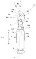
エアロゾル吸引器1は、燃焼を伴わずに香味が付加されたエアロゾルを吸引するための器具であり、所定方向(以下、X方向と称する)に沿って延びる棒形状を有する。エアロゾル吸引器1は、図1及び図2に示すように、X方向に沿って電源ユニット10と、第1カートリッジ20と、第2カートリッジ30と、がこの順に設けられている。第1カートリッジ20は、電源ユニット10に対して着脱可能としてもよく、第2カートリッジ30は、第1カートリッジ20に対して着脱可能である。言い換えると、電源ユニット10に対し、第1カートリッジ20及び第2カートリッジ30は、それぞれ交換可能である。第2カートリッジ30は、第1カートリッジ20に対し、交換可能でもある。なお、第1カートリッジ20を電源ユニット10に対して嵌合させて固定し、ユーザが容易に着脱できない構成としてもよい。
(aerosol inhaler)
The aerosol inhaler 1 is a device for inhaling flavored aerosol without burning, and has a rod shape extending along a predetermined direction (hereinafter referred to as the X direction). As shown in FIGS. 1 and 2, the aerosol inhaler 1 includes a power supply unit 10, a first cartridge 20, and a second cartridge 30 arranged in this order along the X direction. The first cartridge 20 may be detachable from the power supply unit 10 , and the second cartridge 30 is detachable from the first cartridge 20 . In other words, the first cartridge 20 and the second cartridge 30 are replaceable with respect to the power supply unit 10 . The second cartridge 30 is also replaceable with respect to the first cartridge 20 . Alternatively, the first cartridge 20 may be fitted and fixed to the power supply unit 10 so that the user cannot easily attach or detach it.
(電源ユニット)
本実施形態の電源ユニット10は、図3~図5、図7に示すように、円筒状のケース11の内部に、バッテリパックBP、MCU(Micro Controller Unit)50、MCU搭載基板7、レセプタクル搭載基板8等を収容して構成される。
(Power supply unit)
As shown in FIGS. 3 to 5 and 7, the power supply unit 10 of this embodiment includes a battery pack BP, an MCU (Micro Controller Unit) 50, an MCU mounting board 7, and a receptacle mounted inside a cylindrical case 11. It is constructed by accommodating the substrate 8 and the like.
バッテリパックBPに収容される電源BATは、充電可能な二次電池、電気二重層キャパシタ等であり、好ましくは、リチウムイオン二次電池である。電源BATの電解質は、ゲル状の電解質、電解液、固体電解質、イオン液体の1つ又はこれらの組み合わせで構成されていてもよい。
The power supply BAT housed in the battery pack BP is a rechargeable secondary battery, an electric double layer capacitor, etc., preferably a lithium ion secondary battery. The electrolyte of the power supply BAT may be composed of one or a combination of a gel electrolyte, an electrolytic solution, a solid electrolyte, and an ionic liquid.
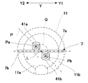
ケース11のX方向の一端側(第1カートリッジ20側)に位置するトップ部11aには、放電端子41が設けられる。放電端子41は、正極側放電端子41a及び負極側放電端子41bから構成される。なお、本明細書において、「正極側」とは、「負極側」よりも高電位側であることを意味する。換言すると、「負極側」とは、「正極側」よりも低電位側であることを意味する。したがって、以下の説明における「正極側」という用語を「高電位側」、「負極側」という用語を「低電位側」、とそれぞれ読み替えてもよい。
A discharge terminal 41 is provided on the top portion 11a located on one end side (first cartridge 20 side) of the case 11 in the X direction. The discharge terminal 41 is composed of a positive discharge terminal 41a and a negative discharge terminal 41b. In this specification, the "positive electrode side" means a higher potential side than the "negative electrode side". In other words, the "negative side" means a lower potential side than the "positive side". Therefore, the term “positive electrode side” and the term “negative electrode side” in the following description may be read as “high potential side” and “low potential side”, respectively.
正極側放電端子41a及び負極側放電端子41bは、トップ部11aから第1カートリッジ20に向かって突出するように設けられ、第1カートリッジ20のヒータ21と電気的に接続可能に構成される。また、ケース11において、トップ部11aの周囲には低床部11bが設けられている。
The positive discharge terminal 41a and the negative discharge terminal 41b are provided so as to protrude from the top portion 11a toward the first cartridge 20, and are configured to be electrically connectable to the heater 21 of the first cartridge 20. Further, in the case 11, a low floor portion 11b is provided around the top portion 11a.
ケース11のX方向の他端側(第1カートリッジ20と反対側)に位置するボトム部11c側の周壁部には、充電端子42へのアクセスを許容する充電用開口43(図2参照)が設けられる。充電端子42は、コンセントやモバイルバッテリ等の外部電源と電気的に接続して電力供給を受けるものであり、本実施形態ではUSB(Universal Serial Bus) Type-C形状のレセプタクルとしているが、これに限定されるものではない。充電用開口43は、ボトム部11c側の周壁部ではなく、ボトム部11c側の底面に設けられてもよい。
A charging opening 43 (see FIG. 2) that allows access to the charging terminal 42 is provided in the peripheral wall portion of the bottom portion 11c located on the other end side of the case 11 in the X direction (the side opposite to the first cartridge 20). be provided. The charging terminal 42 is electrically connected to an external power source such as an outlet or mobile battery to receive power supply, and in this embodiment, it is a USB (Universal Serial Bus) Type-C receptacle. It is not limited. The charging opening 43 may be provided on the bottom surface on the side of the bottom portion 11c instead of on the peripheral wall portion on the side of the bottom portion 11c.
なお、充電端子42は、例えば、受電コイルを備え、外部電源から送電される電力を非接触で受電可能に構成されてもよい。この場合の電力伝送(Wireless Power Transfer)の方式は、電磁誘導型でもよいし、磁気共鳴型でもよいし、電磁誘導型と磁気共鳴型を組み合わせたものでもよい。また、別の一例として、充電端子42は、各種USB端子等が接続可能であり、且つ上記の受電コイルを有していてもよい。このような構成とすることで、電源BATの充電機会を増大できる。
It should be noted that the charging terminal 42 may include, for example, a power receiving coil and be configured to be able to receive power transmitted from an external power source in a non-contact manner. The wireless power transfer method in this case may be an electromagnetic induction type, a magnetic resonance type, or a combination of the electromagnetic induction type and the magnetic resonance type. As another example, the charging terminal 42 may be connectable to various USB terminals or the like, and may have the power receiving coil described above. With such a configuration, the chances of charging the power supply BAT can be increased.
また、ケース11には、ユーザが操作可能な操作部14が、トップ部11aの周壁部に充電用開口43とは反対側を向くように設けられる。操作部14は、ボタン式のスイッチから構成され、ユーザの使用意思を反映してMCU50及び各種センサを起動/遮断する際等に利用される。操作部14は、タッチパネル等から構成されてもよい。
Further, in the case 11, an operation unit 14 that can be operated by the user is provided on the peripheral wall portion of the top portion 11a so as to face the side opposite to the charging opening 43. The operation unit 14 is composed of button-type switches, and is used to activate/deactivate the MCU 50 and various sensors reflecting the user's usage intention. The operation unit 14 may be configured by a touch panel or the like.
また、エアロゾル吸引器1には、各種情報を報知する報知部が設けられている。報知部は、発光素子によって構成されていてもよく、振動素子によって構成されていてもよく、音出力素子によって構成されていてもよい。また、報知部は、発光素子、振動素子及び音出力素子のうち、2以上の素子の組み合わせであってもよい。報知部は、電源ユニット10、第1カートリッジ20、及び第2カートリッジ30のいずれに設けられてもよいが、電源BATからの導線(すなわち配線距離)を短くするため電源ユニット10に設けられることが好ましい。本実施形態の報知部は、操作部14の周囲に設けられたLED窓13、及び後述するLED_L1、LED_L2(図6、図8参照)によって構成される。
In addition, the aerosol inhaler 1 is provided with a notification unit that notifies various information. The notification unit may be configured by a light emitting element, may be configured by a vibration element, or may be configured by a sound output element. Also, the notification unit may be a combination of two or more elements among the light emitting element, the vibration element, and the sound output element. The notification unit may be provided in any of the power supply unit 10, the first cartridge 20, and the second cartridge 30, but is preferably provided in the power supply unit 10 in order to shorten the lead wire (that is, the wiring distance) from the power supply BAT. preferable. The notification unit of the present embodiment includes an LED window 13 provided around the operation unit 14, and LED_L1 and LED_L2 (see FIGS. 6 and 8), which will be described later.
電源ユニット10の内部構成については後述する。
The internal configuration of the power supply unit 10 will be described later.
(第1カートリッジ)
第1カートリッジ20は、図3に示すように、円筒状のカートリッジケース27の内部に、エアロゾル源22を貯留するリザーバ23と、エアロゾル源22を霧化及び/又は気化(以下、単に霧化という)するヒータ21と、リザーバ23からヒータ21へエアロゾル源を引き込むウィック24と、エアロゾル源22が霧化されることで発生したエアロゾルが第2カートリッジ30に向かって流れるエアロゾル流路25と、第2カートリッジ30の一部を収容するエンドキャップ26と、を備える。
(first cartridge)
As shown in FIG. 3, the first cartridge 20 has a reservoir 23 that stores the aerosol source 22 inside a cylindrical cartridge case 27, and atomizes and/or vaporizes the aerosol source 22 (hereinafter simply referred to as atomization). ), a wick 24 that draws the aerosol source from the reservoir 23 to the heater 21, an aerosol flow path 25 through which the aerosol generated by atomizing the aerosol source 22 flows toward the second cartridge 30, a second and an end cap 26 that houses a portion of the cartridge 30 .
リザーバ23は、エアロゾル流路25の周囲を囲むように区画形成され、エアロゾル源22を貯留する。リザーバ23には、樹脂ウェブや綿等の多孔体が収容され、且つ、エアロゾル源22が多孔体に含浸されていてもよい。リザーバ23には、樹脂ウェブ又は綿上の多孔質体が収容されず、エアロゾル源22のみが貯留されていてもよい。エアロゾル源22は、グリセリン、プロピレングリコール、水などの液体を含む。リザーバ23におけるエアロゾル源22の貯留量は、第1カートリッジ20に設けられた残量確認窓28(図1、2参照)から視認可能となっている。残量確認窓28とカートリッジケース27の間には空気取込口となる隙間(図示せず)が形成され、この隙間から外気をカートリッジケース27の内部に取り込む。なお、空気取込口は、必ずしも残量確認窓28の周囲に設けられている必要はない。例えば、電源ユニットに設けられた操作部14とLED窓13の間に隙間を形成し、その隙間から外気をケース11の内部に取り込んでもよいし、充電用開口43を利用してもよい。また、カートリッジケース27やケース11の壁面に内部と外部とを連通する連通孔が設けられていてもよい。
The reservoir 23 is partitioned so as to surround the aerosol flow path 25 and stores the aerosol source 22 . The reservoir 23 may contain a porous material such as a resin web or cotton, and the porous material may be impregnated with the aerosol source 22 . The reservoir 23 may store only the aerosol source 22 without accommodating the resin web or the cotton-like porous body. Aerosol source 22 includes liquids such as glycerin, propylene glycol, and water. The storage amount of the aerosol source 22 in the reservoir 23 can be visually confirmed through a remaining amount confirmation window 28 (see FIGS. 1 and 2) provided in the first cartridge 20 . A gap (not shown) serving as an air intake port is formed between the remaining amount confirmation window 28 and the cartridge case 27, and outside air is drawn into the cartridge case 27 through this gap. It should be noted that the air intake port does not necessarily have to be provided around the remaining amount confirmation window 28 . For example, a gap may be formed between the operation portion 14 provided in the power supply unit and the LED window 13, and outside air may be taken into the case 11 through the gap, or the charging opening 43 may be used. Further, a communication hole may be provided in the wall surface of the cartridge case 27 or the case 11 to communicate the inside and the outside.
ウィック24は、リザーバ23から毛管現象を利用してエアロゾル源22をヒータ21へ引き込む液保持部材であって、例えば、ガラス繊維や多孔質セラミック等によって構成される。
The wick 24 is a liquid holding member that draws the aerosol source 22 from the reservoir 23 into the heater 21 by using capillary action, and is made of, for example, glass fiber or porous ceramic.
ヒータ21は、電源BATから放電端子41を介して供給される電力によって燃焼を伴わずにエアロゾル源22を霧化する。ヒータ21は、所定ピッチで巻き回される電熱線(コイル)によって構成されている。なお、ヒータ21は、エアロゾル源22を霧化してエアロゾルを発生可能な負荷の例示であり、負荷は、例えば、発熱素子、又は超音波発生器である。発熱素子としては、発熱抵抗体、セラミックヒータ、及び誘導加熱式のヒータ等が挙げられる。
The heater 21 atomizes the aerosol source 22 without combustion by power supplied from the power supply BAT via the discharge terminal 41 . The heater 21 is composed of a heating wire (coil) wound at a predetermined pitch. Note that the heater 21 is an example of a load that can generate aerosol by atomizing the aerosol source 22, and the load is, for example, a heating element or an ultrasonic generator. Heating elements include heating resistors, ceramic heaters, induction heaters, and the like.
エアロゾル流路25は、ヒータ21の下流側であって、電源ユニット10(ケース11)の中心線L上に設けられる。なお、この中心線Lは、電源ユニット10(ケース11)をX方向に直交する面で切断した際の電源ユニット10(ケース11)の中心点をX方向に連続してつなげた線である。
The aerosol flow path 25 is provided downstream of the heater 21 and on the center line L of the power supply unit 10 (case 11). The center line L is a line that continuously connects the center points of the power supply unit 10 (case 11) in the X direction when the power supply unit 10 (case 11) is cut along a plane perpendicular to the X direction.
エンドキャップ26は、第2カートリッジ30の一部を収容するカートリッジ収容部26aと、エアロゾル流路25とカートリッジ収容部26aとを連通させる連通路26bと、を備える。
The end cap 26 includes a cartridge accommodating portion 26a that accommodates a portion of the second cartridge 30, and a communicating passage 26b that communicates the aerosol flow path 25 and the cartridge accommodating portion 26a.
(第2カートリッジ)
第2カートリッジ30は、香味源31を貯留する。第2カートリッジ30は、第1カートリッジ20のエンドキャップ26に設けられたカートリッジ収容部26aに着脱可能に収容される。第2カートリッジ30は、第1カートリッジ20側とは反対側の端部が、ユーザの吸口32となっている。なお、吸口32は、第2カートリッジ30と一体不可分に構成される場合に限らず、第2カートリッジ30と着脱可能に構成されてもよい。このように吸口32を電源ユニット10と第1カートリッジ20とは別体に構成することで、吸口32を衛生的に保つことができる。
(second cartridge)
The second cartridge 30 stores the flavor source 31 . The second cartridge 30 is detachably housed in a cartridge housing portion 26 a provided in the end cap 26 of the first cartridge 20 . The second cartridge 30 has a user's mouthpiece 32 at the end opposite to the first cartridge 20 side. It should be noted that the suction port 32 is not limited to being configured integrally with the second cartridge 30 , and may be configured to be detachable from the second cartridge 30 . By constructing the mouthpiece 32 separately from the power supply unit 10 and the first cartridge 20 in this way, the mouthpiece 32 can be kept sanitary.
第2カートリッジ30は、ヒータ21によってエアロゾル源22が霧化されることで発生したエアロゾルを香味源31に通すことによってエアロゾルに香味を付与する。香味源31を構成する原料片としては、刻みたばこ、たばこ原料を粒状に成形した成形体を用いることができる。香味源31は、たばこ以外の植物(例えば、ミント、漢方、ハーブ等)によって構成されてもよい。香味源31には、メントールなどの香料が付与されていてもよい。
The second cartridge 30 passes the aerosol generated by atomizing the aerosol source 22 by the heater 21 through the flavor source 31 to add flavor to the aerosol. As the raw material piece constituting the flavor source 31, cut tobacco or a molded body obtained by molding tobacco raw material into granules can be used. The flavor source 31 may be composed of plants other than tobacco (for example, mint, Chinese medicine, herbs, etc.). The flavor source 31 may be provided with a flavor such as menthol.
本実施形態のエアロゾル吸引器1では、エアロゾル源22と香味源31とヒータ21とによって、香味が付加されたエアロゾルを発生させることができる。つまり、エアロゾル源22と香味源31は、エアロゾルを発生させるエアロゾル生成源ということができる。
In the aerosol inhaler 1 of this embodiment, the aerosol with added flavor can be generated by the aerosol source 22, the flavor source 31, and the heater 21. That is, the aerosol source 22 and the flavor source 31 can be said to be aerosol generating sources that generate aerosol.
エアロゾル吸引器1に用いられるエアロゾル生成源の構成は、エアロゾル源22と香味源31とが別体になっている構成の他、エアロゾル源22と香味源31とが一体的に形成されている構成、香味源31が省略されて香味源31に含まれ得る物質がエアロゾル源22に付加された構成、香味源31の代わりに薬剤等がエアロゾル源22に付加された構成等であってもよい。
The configuration of the aerosol generation source used in the aerosol inhaler 1 includes a configuration in which the aerosol source 22 and the flavor source 31 are separated, and a configuration in which the aerosol source 22 and the flavor source 31 are integrally formed. , a configuration in which the flavor source 31 is omitted and a substance that can be contained in the flavor source 31 is added to the aerosol source 22, or a configuration in which a drug or the like is added to the aerosol source 22 instead of the flavor source 31.
このように構成されたエアロゾル吸引器1では、ヒータ21が、ウィック24によってリザーバ23から引き込まれた又は移動させられたエアロゾル源22を霧化する。霧化されて発生したエアロゾルは、残量確認窓28とカートリッジケース27の間に形成された空気取込口となる隙間(図示せず)から流入した空気と共にエアロゾル流路25を流れ、連通路26bを介して第2カートリッジ30に供給される。第2カートリッジ30に供給されたエアロゾルは、香味源31を通過することで香味が付与され、吸口32に供給される。
In the aerosol inhaler 1 configured in this way, the heater 21 atomizes the aerosol source 22 drawn or displaced from the reservoir 23 by the wick 24 . The aerosol generated by atomization flows through the aerosol flow path 25 together with the air that has flowed in from a gap (not shown) that serves as an air intake port formed between the remaining amount confirmation window 28 and the cartridge case 27, and flows through the communication path. 26b to the second cartridge 30. The aerosol supplied to the second cartridge 30 is flavored by passing through the flavor source 31 and supplied to the mouthpiece 32 .
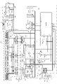
(電源ユニット10の回路構成)
続いて、電源ユニット10の回路構成について図6を参照しながら説明する。
図6において、一点鎖線で囲んだ範囲内に図示した電子部品は、レセプタクル搭載基板8に実装された電子部品である。すなわち、レセプタクル搭載基板8は、主要な電子部品として、USB Type-Cのプラグ(以下、単にUSBプラグともいう)を挿入可能なレセプタクルである充電端子42と、レセプタクル搭載基板8とMCU搭載基板7とを接続する基板接続ケーブルCb1の一端が接続されるレセプタクル搭載基板側コネクタCn1と、を備える。本実施形態では、基板接続ケーブルCb1を、6本のプリントパターンを有するFPC(Flexible Printed Circuit)ケーブルとするが、これに限定されるものではない。
(Circuit Configuration of Power Supply Unit 10)
Next, the circuit configuration of the power supply unit 10 will be described with reference to FIG.
In FIG. 6 , the electronic parts shown within the range surrounded by the dashed line are the electronic parts mounted on the receptacle mounting substrate 8 . That is, the receptacle mounting board 8 includes, as main electronic components, a charging terminal 42 which is a receptacle into which a USB Type-C plug (hereinafter simply referred to as a USB plug) can be inserted, the receptacle mounting board 8, and the MCU mounting board 7. and a receptacle mounting board-side connector Cn1 to which one end of a board connection cable Cb1 for connecting the receptacle mounting board side connector Cn1 is connected. In this embodiment, the board connection cable Cb1 is an FPC (Flexible Printed Circuit) cable having six printed patterns, but it is not limited to this.
また、図6において、二点鎖線で囲んだ範囲内に図示した電子部品は、MCU搭載基板7に実装された電子部品である。すなわち、MCU搭載基板7は、主要な電子部品として、基板接続ケーブルCb1の他端が接続されるMCU搭載基板側コネクタCn2と、電源ユニット10を含むエアロゾル吸引器1全体を統括制御するMCU50と、電源BATの充電等を行う充電IC(Integrated Circuit)55と、充電IC55を保護する保護IC61と、MCU50等に対して所定の電圧を供給するLDO(Low Dropout)レギュレータ62と、ユーザのパフ(吸引)動作を検出するための吸引センサ15と、ヒータ21が接続される放電端子41(41a、41b)と、放電端子41に電力を供給可能なDC/DCコンバータ63と、バッテリパックBPとMCU搭載基板7とを接続するバッテリ接続ケーブルCb2が接続されるバッテリコネクタCn3と、を備える。
In addition, in FIG. 6, the electronic parts shown within the range surrounded by the two-dot chain line are the electronic parts mounted on the MCU mounting board 7 . That is, the MCU-mounted board 7 includes, as main electronic components, an MCU-mounted board-side connector Cn2 to which the other end of the board connection cable Cb1 is connected, an MCU 50 that controls the entire aerosol inhaler 1 including the power supply unit 10, A charging IC (Integrated Circuit) 55 that charges the power supply BAT, etc., a protection IC 61 that protects the charging IC 55, an LDO (Low Dropout) regulator 62 that supplies a predetermined voltage to the MCU 50, etc., and a user's puff (suction). ) a suction sensor 15 for detecting operation, a discharge terminal 41 (41a, 41b) to which a heater 21 is connected, a DC/DC converter 63 capable of supplying power to the discharge terminal 41, a battery pack BP and an MCU. and a battery connector Cn3 to which a battery connection cable Cb2 connecting with the board 7 is connected.
MCU50、充電IC55、保護IC61、LDOレギュレータ62、吸引センサ15、及びDC/DCコンバータ63は、例えば、複数の回路素子をチップ化して構成され、自装置の内部と外部とを電気的に接続するための端子としてのピンを備える。これらチップ化された各電子部品が備えるピンの詳細については後述する。なお、本明細書等では、これらチップ化された各電子部品が備えるピンのうち主要なピンのみを記載している点に留意されたい。
The MCU 50, the charging IC 55, the protection IC 61, the LDO regulator 62, the suction sensor 15, and the DC/DC converter 63 are configured by, for example, chipping a plurality of circuit elements, and electrically connect the inside and outside of the device. A pin is provided as a terminal for The details of the pins included in each of these chipped electronic components will be described later. It should be noted that, in this specification and the like, only major pins among the pins included in each of these chipped electronic components are described.
バッテリパックBPは、電源BATと、電源BATの正極端子に接続されるヒューズFSと、電源BATの負極端子に接続され且つ電源BATに近接配置されたサーミスタTHと、を備える。サーミスタTHは、NTC(Negative Temperature Coefficient:負の抵抗温度係数)特性あるいはPTC(Positive Temperature Coefficient:正の抵抗温度係数)特性を有する素子、すなわち、電気抵抗値と温度とに相関を持つ素子を主体に構成される。また、本実施形態では、バッテリパックBPとMCU搭載基板7とを接続するバッテリ接続ケーブルCb2を、3本のプリントパターンを有するFPCケーブルとするが、これに限定されるものではない。バッテリ接続ケーブルCb2は3本のワイヤで接続されていてもよい。
The battery pack BP includes a power supply BAT, a fuse FS connected to the positive terminal of the power supply BAT, and a thermistor TH connected to the negative terminal of the power supply BAT and arranged close to the power supply BAT. The thermistor TH is mainly an element having NTC (Negative Temperature Coefficient) characteristics or PTC (Positive Temperature Coefficient) characteristics, that is, an element that has a correlation between electrical resistance and temperature. configured to Also, in the present embodiment, the battery connection cable Cb2 that connects the battery pack BP and the MCU mounting board 7 is an FPC cable having three printed patterns, but it is not limited to this. The battery connection cable Cb2 may be connected with three wires.
図6において、太い実線で示す配線は、電源ユニット10に設けられたグランドに接続された配線(例えば、後述するグランドパターン78等により構成される配線)である。すなわち、この配線は、電源ユニット10において基準となる電位(グランド電位)と同電位になる配線であり、以下、グランドラインともいう。
In FIG. 6, the wiring indicated by the thick solid line is the wiring connected to the ground provided in the power supply unit 10 (for example, the wiring configured by the ground pattern 78 described later). In other words, this wiring has the same potential as the reference potential (ground potential) in the power supply unit 10, and is hereinafter also referred to as a ground line.
また、電源ユニット10には、グランドライン以外の主要な配線として、VBUSラインLn1と、VBATラインLn2と、D+ラインLn3aと、D-ラインLn3bと、パワーパス(Power-Path)ラインLn4と、VSYSラインLn5と、VHEATラインLn6とが設けられる。これらの各ライン(配線)は、MCU搭載基板7に形成された導電パターンを主体に構成される。これら各ラインに接続される電子部品については後述する。
In the power supply unit 10, main wirings other than the ground line include a VBUS line Ln1, a VBAT line Ln2, a D+ line Ln3a, a D− line Ln3b, a power-path line Ln4, and a VSYS line Ln4. A line Ln5 and a VHEAT line Ln6 are provided. Each of these lines (wiring) is mainly composed of a conductive pattern formed on the MCU mounting board 7 . Electronic components connected to these lines will be described later.
なお、以下では、レセプタクル搭載基板8とMCU搭載基板7とを接続する電子部品である、基板接続ケーブルCb1と、レセプタクル搭載基板側コネクタCn1と、MCU搭載基板側コネクタCn2とを合わせて、基板接続部CNとも称する。
In the following description, a board connection cable Cb1, a receptacle mounting board-side connector Cn1, and an MCU mounting board-side connector Cn2, which are electronic components that connect the receptacle mounting board 8 and the MCU mounting board 7, are combined to form a board connection. Also referred to as part CN.
(充電端子及び保護IC)
充電端子42は、挿入されたUSBプラグのA1ピン、A4ピン、A5ピン、A6ピン、A7ピン、A8ピン、A9ピン、A12ピン、B1ピン、B4ピン、B5ピン、B6ピン、B7ピン、B8ピン、B9ピン、及びB12ピンの各ピンにそれぞれ接続されるピン(端子)を備える。本明細書等では、USBプラグのAnピン(ただしn=1~12)に対応する充電端子42のピンを、充電端子42のAnピンともいう。同様に、USBプラグのBnピンに対応する充電端子42のピンを、充電端子42のBnピンともいう。
(Charging terminal and protection IC)
The charging terminals 42 are the A1 pin, A4 pin, A5 pin, A6 pin, A7 pin, A8 pin, A9 pin, A12 pin, B1 pin, B4 pin, B5 pin, B6 pin, B7 pin, It has pins (terminals) connected to the B8 pin, B9 pin, and B12 pin, respectively. In this specification and the like, the pins of the charging terminal 42 corresponding to the An pins (where n=1 to 12) of the USB plug are also called the An pins of the charging terminal 42 . Similarly, the pin of the charging terminal 42 corresponding to the Bn pin of the USB plug is also called the Bn pin of the charging terminal 42 .
USBプラグのGND(グランド)ピンに対応する充電端子42のA1ピン、A12ピン、B1ピン、及びB12ピンは、グランドラインに接続される。
The A1 pin, A12 pin, B1 pin, and B12 pin of the charging terminal 42 corresponding to the GND (ground) pin of the USB plug are connected to the ground line.
USBプラグのVBUSピンに対応する充電端子42のA4ピン、A9ピン、B4ピン、及びB9ピンは、基板接続部CN、VBUSラインLn1、及び保護IC61を介して、充電IC55の高電位側の電源端子であるVBUSピンに接続される。これにより、充電端子42のA4ピン、A9ピン、B4ピン、あるいはB9ピンを介して電源ユニット10へ入力された外部電源からの電力(例えばUSBバスパワー)を充電IC55に供給でき、この電力を用いた充電IC55による電源BATの充電やMCU50への電力供給を可能にする。
The A4 pin, A9 pin, B4 pin, and B9 pin of the charging terminal 42 corresponding to the V BUS pin of the USB plug are connected to the high potential side of the charging IC 55 via the board connection portion CN, the VBUS line Ln1, and the protection IC 61. It is connected to the VBUS pin, which is a power supply terminal. As a result, power (for example, USB bus power) from an external power supply input to the power supply unit 10 via the A4 pin, A9 pin, B4 pin, or B9 pin of the charging terminal 42 can be supplied to the charging IC 55. The charging IC 55 used can charge the power supply BAT and supply power to the MCU 50 .
充電端子42と充電IC55との間に設けられる保護IC61について詳述すると、保護IC61は、高電位側の電源端子であるINピンと、低電位側の電源端子であるVSSピンと、グランドされるGNDピンと、後述の第1システム電圧Vs1が出力される出力端子であるOUTピンと、保護IC61の動作をオンにしたりオフにしたりする(以下、オン/オフするともいう)ためのCEピンと、電源BATの接続状態を検知するためのVBATピンと、を備える。
The protection IC 61 provided between the charging terminal 42 and the charging IC 55 is detailed. , an OUT pin that is an output terminal for outputting a first system voltage Vs1 to be described later, a CE pin for turning on and off the operation of the protection IC 61 (hereinafter also referred to as on/off), and a power supply BAT. and a VBAT pin for sensing the state.
充電端子42のA4ピン及びB9ピンと、A9ピン及びB4ピンとは、基板接続部CN及びVBUSラインLn1を介して、保護IC61のINピンに対して並列に接続される。換言すると、保護IC61のINピンは、充電端子42のA4ピン及びB9ピンと、A9ピン及びB4ピンとのそれぞれに接続される。保護IC61のVSSピン、GNDピン、及びCEピンは、グランドラインに接続される。保護IC61のOUTピンは、充電IC55のVBUSピンに接続される。保護IC61のVBATピンは、VBATラインLn2、バッテリコネクタCn3、バッテリ接続ケーブルCb2、及びヒューズFSを介して、電源BATの正極端子(すなわち高電位側)に接続される。なお、電源BATの負極端子(すなわち低電位側)は、バッテリ接続ケーブルCb2及びバッテリコネクタCn3を介して、グランドラインに接続される。
The A4 pin and B9 pin of the charging terminal 42 and the A9 pin and B4 pin are connected in parallel to the IN pin of the protection IC 61 via the board connection portion CN and the VBUS line Ln1. In other words, the IN pin of the protection IC 61 is connected to the A4 pin and B9 pin of the charging terminal 42 and the A9 pin and B4 pin, respectively. The VSS pin, GND pin and CE pin of the protection IC 61 are connected to the ground line. The OUT pin of protection IC 61 is connected to the VBUS pin of charging IC 55 . The VBAT pin of the protection IC 61 is connected to the positive terminal (that is, high potential side) of the power supply BAT via the VBAT line Ln2, battery connector Cn3, battery connection cable Cb2, and fuse FS. The negative terminal (that is, the low potential side) of the power supply BAT is connected to the ground line via the battery connection cable Cb2 and the battery connector Cn3.
保護IC61は、INピンの電位とVSSピンの電位との差分により電源電圧が供給され、且つCEピンへの入力がローレベルであるときに動作して、所定の第1システム電圧Vs1をOUTピンから出力したり、VBATピンへの入力電圧に基づき電源BATが接続されているか否かを検知したりする。本実施形態における充電IC61は、CEピンへローレベルが入力されることでイネーブルされることから、負論理動作である。これに代えて、CEピンへハイレベルが入力されることでイネーブルされる正論理動作の保護IC61を用いてもよい。この場合、CEピンへハイレベルが入力されるように、CEピンはINピンへ接続されることが好ましい。
The protection IC 61 is supplied with a power supply voltage based on the difference between the potential of the IN pin and the potential of the VSS pin, and operates when the input to the CE pin is at a low level to apply a predetermined first system voltage Vs1 to the OUT pin. and detects whether the power supply BAT is connected based on the input voltage to the VBAT pin. The charging IC 61 in the present embodiment is enabled by inputting a low level to the CE pin, and therefore performs negative logic operation. Alternatively, a positive logic protection IC 61 that is enabled by inputting a high level to the CE pin may be used. In this case, the CE pin is preferably connected to the IN pin so that a high level is input to the CE pin.
より詳細に説明すると、充電端子42にUSBプラグが挿入され、且つ、このUSBプラグを含むUSBケーブルが外部電源に接続されると、充電端子42のA4ピン、A9ピン、B4ピン、及びB9ピンには、外部電源から所定のUSB電圧(例えば5[V])が供給される。これにより、このUSB電圧が電源電圧として保護IC61に供給される。また、保護IC61のCEピンはグランドされているため、このCEピンへの入力電圧は常にローレベルとなる。したがって、保護IC61は、充電端子42を介して外部電源からUSB電圧が供給されたことに応じて、第1システム電圧Vs1を充電IC55に対して出力する。
More specifically, when a USB plug is inserted into the charging terminal 42 and a USB cable including this USB plug is connected to an external power supply, pins A4, A9, B4 and B9 of the charging terminal 42 are connected. is supplied with a predetermined USB voltage (for example, 5 [V]) from an external power supply. As a result, this USB voltage is supplied to the protection IC 61 as a power supply voltage. Also, since the CE pin of the protection IC 61 is grounded, the input voltage to this CE pin is always low level. Therefore, the protection IC 61 outputs the first system voltage Vs1 to the charging IC 55 in response to the USB voltage being supplied from the external power supply via the charging terminal 42 .
保護IC61が出力する第1システム電圧Vs1は、充電IC55の推奨入力電圧の範囲(例えば4.35~6.4[V]の範囲)に含まれる電圧値を有する。
The first system voltage Vs1 output by the protection IC 61 has a voltage value within the recommended input voltage range of the charging IC 55 (for example, the range of 4.35 to 6.4 [V]).
例えば、保護IC61は、INピンへの入力電圧(換言するとINピンの電位)が充電IC55の推奨入力電圧の範囲に含まれる場合には、INピンへの入力電圧を第1システム電圧Vs1としてそのままOUTピンから出力する。一方、保護IC61は、INピンへの入力電圧が充電IC55の推奨入力電圧の最大値を上回る場合には、INピンへの入力電圧から充電IC55の推奨入力電圧の範囲に含まれる所定の電圧(例えば5.5±0.2[V])に変換し、変換した電圧を第1システム電圧Vs1としてOUTピンから出力する。これにより、充電IC55の推奨入力電圧の最大値を上回るような高電圧が保護IC61へ入力されたとしても、この高電圧が保護IC61から充電IC55に出力されるのを回避して、この高電圧から充電IC55を保護することが可能となる。
For example, when the input voltage to the IN pin (in other words, the potential of the IN pin) is included in the recommended input voltage range of the charging IC 55, the protection IC 61 uses the input voltage to the IN pin as the first system voltage Vs1 as it is. Output from the OUT pin. On the other hand, when the input voltage to the IN pin exceeds the maximum value of the recommended input voltage of the charging IC 55, the protection IC 61 detects a predetermined voltage ( For example, 5.5±0.2 [V]), and the converted voltage is output from the OUT pin as the first system voltage Vs1. As a result, even if a high voltage exceeding the maximum value of the recommended input voltage of the charging IC 55 is input to the protection IC 61 , this high voltage is prevented from being output from the protection IC 61 to the charging IC 55 . It is possible to protect the charging IC 55 from the
なお、保護IC61は、充電IC55の推奨入力電圧の最大値を上回るような高電圧がINピンに入力された場合には、INピンとOUTピンとを接続する保護IC61内の回路(不図示)を開くことで、INピンに入力された高電圧がOUTピンから出力されないようにしてもよい。
The protection IC 61 opens a circuit (not shown) in the protection IC 61 that connects the IN pin and the OUT pin when a high voltage exceeding the maximum value of the recommended input voltage of the charging IC 55 is input to the IN pin. Thus, the high voltage input to the IN pin may be prevented from being output from the OUT pin.
また、前述したように、保護IC61は、VBATピンへの入力電圧に基づき電源BATが接続されているか否かを検知することが可能である。保護IC61は、電源BATが接続されているか否かの検知結果を、自装置で利用してもよいし、自装置の外部(例えばMCU50あるいは充電IC55)へ出力してもよい。さらに、保護IC61は、前述した充電IC55を保護する機能のほか、例えば過電流検知機能や過電圧検知機能等、電源ユニット10の電気回路を保護するための各種保護機能を有していてもよい。
Also, as described above, the protection IC 61 can detect whether or not the power supply BAT is connected based on the input voltage to the VBAT pin. The protection IC 61 may use the detection result of whether or not the power supply BAT is connected in its own device, or may output it to the outside of its own device (for example, the MCU 50 or the charging IC 55). Furthermore, the protection IC 61 may have various protection functions for protecting the electric circuit of the power supply unit 10, such as an overcurrent detection function and an overvoltage detection function, in addition to the function of protecting the charging IC 55 described above.
また、図6に示すように、VBUSラインLn1には、保護IC61のINピンへの入力を安定化(平滑化)するためのコンデンサ(平滑コンデンサあるいはバイパスコンデンサとも称される)Cd1が必要に応じて適宜接続される。同様に、保護IC61のOUTピンと充電IC55のVBUSピンとの間には、充電IC55のVBUSピンへの入力(すなわち保護IC61から出力された第1システム電圧Vs1)を安定化するためのコンデンサCd2が必要に応じて適宜接続される。
As shown in FIG. 6, a capacitor (also called a smoothing capacitor or a bypass capacitor) Cd1 for stabilizing (smoothing) the input to the IN pin of the protection IC 61 is connected to the VBUS line Ln1 as needed. connected as appropriate. Similarly, a capacitor Cd2 is required between the OUT pin of the protection IC 61 and the VBUS pin of the charging IC 55 to stabilize the input to the VBUS pin of the charging IC 55 (that is, the first system voltage Vs1 output from the protection IC 61). are connected as appropriate.
ところで、保護IC61のINピンと接続される充電端子42のA4ピン、A9ピン、B4ピン、及びB9ピンは、バリスタ(Variable Resistor:非直線性抵抗素子)VR1を介して、グランドラインとも接続される。このように、バリスタVR1を介して、充電端子42のA4ピン、A9ピン、B4ピン、及びB9ピンをグランドラインと接続しておくことで、充電端子42へのUSBプラグ挿入時にこれらが擦れる等して充電端子42のA4ピン、A9ピン、B4ピン、あるいはB9ピンに静電気が発生しても、この静電気を、バリスタVR1を介してグランドラインへ逃がすことができる。したがって、充電端子42のA4ピン、A9ピン、B4ピン、あるいはB9ピンに発生した静電気から保護IC61を保護することが可能となる。
By the way, the A4 pin, A9 pin, B4 pin, and B9 pin of the charging terminal 42 connected to the IN pin of the protection IC 61 are also connected to the ground line via a varistor (Variable Resistor: non-linear resistance element) VR1. . By connecting the A4 pin, A9 pin, B4 pin, and B9 pin of the charging terminal 42 to the ground line via the varistor VR1 in this way, it is possible to prevent friction between these pins when the USB plug is inserted into the charging terminal 42. Even if static electricity is generated at the A4 pin, A9 pin, B4 pin, or B9 pin of the charging terminal 42, this static electricity can be released to the ground line via the varistor VR1. Therefore, it is possible to protect the protection IC 61 from static electricity generated at the A4 pin, A9 pin, B4 pin, or B9 pin of the charging terminal 42 .
USBプラグのDp(D+ともいう)1ピンあるいはDp2ピンに対応する充電端子42のA6ピン及びB6ピンは、基板接続部CN及びD+ラインLn3aを介して、MCU50のPA11ピンに接続される。また、USBプラグのDn(D-ともいう)1ピンあるいはDp2ピンに対応する充電端子42のA7ピン及びB7ピンは、基板接続部CN及びD-ラインLn3bを介して、MCU50のPA12ピンに接続される。これにより、充電端子42に挿入されたUSBプラグを含むUSBケーブルが接続された外部機器(以下、単に、外部機器ともいう)とMCU50との間で、例えば、D+ラインLn3a及びD-ラインLn3bの2つの信号線を用いたシリアル通信を行うことを可能にする。なお、外部機器とMCU50との間の通信には、シリアル通信以外の通信方式を採用してもよい。
The A6 pin and B6 pin of the charging terminal 42 corresponding to the Dp (also called D+) 1 pin or Dp2 pin of the USB plug are connected to the PA11 pin of the MCU 50 via the board connection portion CN and the D+ line Ln3a. Also, the A7 pin and B7 pin of the charging terminal 42 corresponding to the Dn (also called D-) 1 pin or Dp2 pin of the USB plug are connected to the PA12 pin of the MCU 50 via the board connection portion CN and the D- line Ln3b. be done. As a result, between the MCU 50 and the external device to which the USB cable including the USB plug inserted into the charging terminal 42 (hereinafter simply referred to as the external device), for example, the D+ line Ln3a and the D− line Ln3b are connected. It enables serial communication using two signal lines. Communication methods other than serial communication may be used for communication between the external device and the MCU 50 .
また、MCU50のPA11ピンと接続される充電端子42のA6ピン及びB6ピンは、バリスタVR2を介して、グランドラインとも接続される。これにより、充電端子42のA6ピンあるいはB6ピンに静電気が発生しても、この静電気を、バリスタVR2を介してグランドラインへ逃がすことができる。したがって、充電端子42のA6あるいはB6ピンに発生した静電気からMCU50を保護することが可能となる。
Also, the A6 pin and B6 pin of the charging terminal 42 connected to the PA11 pin of the MCU 50 are also connected to the ground line via the varistor VR2. As a result, even if static electricity is generated at the A6 pin or B6 pin of the charging terminal 42, the static electricity can be released to the ground line via the varistor VR2. Therefore, it is possible to protect the MCU 50 from static electricity generated at the A6 or B6 pin of the charging terminal 42 .
さらに、図6に示すように、充電端子42のA6ピン及びB6ピンと、MCU50のPA11ピンとの間に抵抗器R11を設ければ、MCU50のPA11ピンに大電流が入力されるのを抵抗器R11によって抑制することが可能となる。なお、本明細書等において、抵抗器とは、抵抗素子やトランジスタ等により構成された所定の電気抵抗値を有する素子である。
Furthermore, as shown in FIG. 6, if a resistor R11 is provided between the A6 and B6 pins of the charging terminal 42 and the PA11 pin of the MCU 50, the large current input to the PA11 pin of the MCU 50 can be prevented by the resistor R11. can be suppressed by In this specification and the like, a resistor is an element having a predetermined electrical resistance value, which is composed of a resistive element, a transistor, or the like.
また、MCU50のPA12ピンと接続される充電端子42のA7ピン及びB7ピンは、バリスタVR3を介して、グランドラインとも接続される。これにより、充電端子42のA7ピンあるいはB7ピンに静電気が発生しても、この静電気を、バリスタVR3を介してグランドラインへ逃がすことができる。したがって、充電端子42のA7ピンあるいはB7ピンに発生した静電気からMCU50を保護することが可能となる。
Also, the A7 pin and B7 pin of the charging terminal 42 connected to the PA12 pin of the MCU 50 are also connected to the ground line via the varistor VR3. As a result, even if static electricity is generated at the A7 pin or the B7 pin of the charging terminal 42, the static electricity can be released to the ground line via the varistor VR3. Therefore, it is possible to protect the MCU 50 from static electricity generated at the A7 pin or the B7 pin of the charging terminal 42 .
さらに、図6に示すように、充電端子42のA7ピン及びB7ピンと、MCU50のPA12ピンとの間に抵抗器R12を設ければ、MCU50のPA12ピンに大電流が入力されるのを抵抗器R12によって抑制することが可能となる。
Furthermore, as shown in FIG. 6, if a resistor R12 is provided between the A7 and B7 pins of the charging terminal 42 and the PA12 pin of the MCU 50, the large current input to the PA12 pin of the MCU 50 can be prevented by the resistor R12. can be suppressed by
また、電源ユニット10では、USBプラグが充電端子42にアップサイドアップの向きで挿入されたのかアップサイドダウンの向きで挿入されたのかを、MCU50が認識しなくても問題は生じない。このため、USBプラグのCC1ピンあるいはCC2ピンに対応する充電端子42のA5ピン及びB5ピンは、グランドラインに接続される。さらに、USBプラグのSBU1ピンあるいはSBU2ピンに対応する充電端子42のA8ピン及びB8ピンにあっては、電源ユニット10の電気回路と接続されていない。すなわち、これら充電端子42のピンは、電源ユニット10において利用されていないため、適宜省略することも可能である。このようにすることで、電源ユニット10の回路構成が複雑化することを抑制できる。
Also, in the power supply unit 10, there is no problem even if the MCU 50 does not recognize whether the USB plug is inserted into the charging terminal 42 in the upside-up direction or the upside-down direction. Therefore, the A5 pin and B5 pin of the charging terminal 42 corresponding to the CC1 pin or CC2 pin of the USB plug are connected to the ground line. Furthermore, the A8 pin and B8 pin of the charging terminal 42 corresponding to the SBU1 pin or SBU2 pin of the USB plug are not connected to the electric circuit of the power supply unit 10 . That is, since these pins of the charging terminal 42 are not used in the power supply unit 10, they can be omitted as appropriate. By doing so, it is possible to prevent the circuit configuration of the power supply unit 10 from becoming complicated.
(充電IC)
充電IC55は、高電位側の電源端子の1つであるVBUSピンと、低電位側の電源端子であるGNDピンと、充電IC55と電源BATとの間の電力授受に用いられる入出力端子であるBAT_1ピン及びBAT_2ピンと、電源BATへの入力あるいは電源BATからの出力を検出する検出端子としてのBAT_SNSピンと、後述の第2システム電圧Vs2が出力される出力端子であるSYS_1、SYS_2ピン、SW_1ピン、及びSW_2ピンと、充電IC55の動作をオン/オフするためのCEピンと、を含んで構成される。なお、BAT_1ピン及びBAT_2ピンも、充電IC55における高電位側の電源端子として機能し得る。
(charging IC)
The charging IC 55 has a VBUS pin, which is one of power supply terminals on the high potential side, a GND pin, which is a power supply terminal on the low potential side, and a BAT_1 pin, which is an input/output terminal used for power transfer between the charging IC 55 and the power supply BAT. and a BAT_2 pin, a BAT_SNS pin as a detection terminal for detecting input to or output from the power supply BAT, and SYS_1, SYS_2, SW_1, and SW_2 as output terminals for outputting a second system voltage Vs2 described later. and a CE pin for turning on/off the operation of the charging IC 55 . Note that the BAT_1 pin and the BAT_2 pin can also function as high-potential-side power supply terminals in the charging IC 55 .
充電IC55のVBUSピンは、前述したように、保護IC61のOUTピンに接続される。充電IC55のBAT_1ピン、BAT_2ピン、及びBAT_SNSピンは、VBATラインLn2、バッテリコネクタCn3、バッテリ接続ケーブルCb2、及びヒューズFSを介して、電源BATの正極端子に接続される。充電IC55のSYS_1ピン、SYS_2ピン、SW_1ピン、及びSW_2ピンは、パワーパスラインLn4を介して、LDOレギュレータ62の高電位側の電源端子であるINピンと、DC/DCコンバータ63の高電位側の電源端子であるVINピンとに接続される。なお、SW_1ピン及びSW_2ピンは、リアクトルRc1を介して、パワーパスラインLn4に接続される。また、充電IC55のCEピンは、MCU50のPB14ピンに接続される。
The VBUS pin of the charging IC 55 is connected to the OUT pin of the protection IC 61 as described above. The BAT_1 pin, BAT_2 pin, and BAT_SNS pin of the charging IC 55 are connected to the positive terminal of the power supply BAT via the VBAT line Ln2, battery connector Cn3, battery connection cable Cb2, and fuse FS. The SYS_1 pin, SYS_2 pin, SW_1 pin, and SW_2 pin of the charging IC 55 are connected via the power path line Ln4 to the IN pin, which is the power supply terminal on the high potential side of the LDO regulator 62, and the high potential side of the DC/DC converter 63. It is connected to the VIN pin which is a power supply terminal. The SW_1 pin and the SW_2 pin are connected to the power path line Ln4 via the reactor Rc1. Also, the CE pin of the charging IC 55 is connected to the PB14 pin of the MCU 50 .
充電IC55は、VBUSピン、BAT_1ピン、あるいはBAT_2ピンの電位とGNDピンの電位との差分により電源電圧が供給され、且つCEピンへの入力がハイレベルであるときに動作して、電源BATの充電を行ったり、電源BATから放電された電力をLDOレギュレータ62やDC/DCコンバータ63等に供給したりする。本実施形態における充電IC55は、CEピンへハイレベルが入力されることでイネーブルされることから、正論理動作である。これに代えて、CEピンへローレベルが入力されることでイネーブルされる負論理動作の充電IC55を用いてもよい。
The charging IC 55 is supplied with a power supply voltage based on the difference between the potential of the VBUS pin, BAT_1 pin, or BAT_2 pin and the potential of the GND pin, and operates when the input to the CE pin is at a high level. It performs charging, and supplies power discharged from the power supply BAT to the LDO regulator 62, the DC/DC converter 63, and the like. The charging IC 55 in this embodiment is enabled by inputting a high level to the CE pin, and therefore operates in positive logic. Alternatively, a negative logic charging IC 55 that is enabled by inputting a low level to the CE pin may be used.
より詳細に説明すると、充電IC55は、VBUSピンに第1システム電圧Vs1が入力されると、BAT_1ピン及びBAT_2ピンから電源BATに対して電源BATを充電するための電圧(例えば第1システム電圧Vs1)を出力する。一方、電源BATの放電時には、電源BATの出力電圧(端子電圧)がBAT_1ピン及びBAT_2ピンに入力される。この場合、充電IC55は、BAT_1ピン及びBAT_2ピンへの入力電圧に応じた第2システム電圧Vs2を、SYS_1ピン、SYS_2ピン、SW_1ピン、及びSW_2ピンから、LDOレギュレータ62やDC/DCコンバータ63等に対して出力する。第2システム電圧Vs2は、例えば、電源BATの出力電圧そのものであり、具体的には3~4[V]程度の電圧とすることができる。
More specifically, when the first system voltage Vs1 is input to the VBUS pin, the charging IC 55 applies a voltage (for example, the first system voltage Vs1 ). On the other hand, when the power supply BAT is discharged, the output voltage (terminal voltage) of the power supply BAT is input to the BAT_1 pin and the BAT_2 pin. In this case, the charging IC 55 applies the second system voltage Vs2 according to the input voltages to the BAT_1 pin and the BAT_2 pin from the SYS_1 pin, the SYS_2 pin, the SW_1 pin, and the SW_2 pin to the LDO regulator 62, DC/DC converter 63, etc. Output for The second system voltage Vs2 is, for example, the output voltage itself of the power supply BAT, and specifically can be a voltage of about 3 to 4 [V].
また、充電IC55は、MCU50のPB8ピンに接続されるSCLピンと、MCU50のPB9ピンに接続されるSDAピンと、をさらに備える。これにより、充電IC55とMCU50との間で、例えばI2C(Inter-Integrated Circuit)通信を行うことが可能である。この通信を利用して、充電IC55は、例えば、電源BATに関するバッテリ情報をMCU50に送信する。ここで、バッテリ情報は、例えば、充電IC55による電源BATの充電状態(例えば充電中もしくは充電停止中)や、電源BATの残量(SOC:State Of Charge)等をあらわす情報である。なお、充電IC55とMCU50との間の通信には、I2C通信以外の通信方式を採用してもよい。
The charging IC 55 further includes an SCL pin connected to the PB8 pin of the MCU50 and an SDA pin connected to the PB9 pin of the MCU50. Thereby, for example, I2C (Inter-Integrated Circuit) communication can be performed between the charging IC 55 and the MCU 50 . Using this communication, the charging IC 55 transmits, for example, battery information regarding the power supply BAT to the MCU 50 . Here, the battery information is, for example, information indicating the charging state of the power supply BAT by the charging IC 55 (for example, charging or charging stopped), the remaining amount of the power supply BAT (SOC: State Of Charge), and the like. Communication between the charging IC 55 and the MCU 50 may employ a communication method other than the I2C communication.
また、図6に示すように、充電IC55は、ISETピン、ILIMピン、TSピン等をさらに備えてもよい。充電IC55がISETピンを備える場合、このISETピンとグランドラインとの間に接続される抵抗器の電気抵抗値により、充電IC55から電源BATに対して出力される電流値を設定可能である。充電IC55がILIMピンを備える場合、このILIMピンとグランドラインとの間に接続される抵抗器の電気抵抗値により、充電IC55からLDOレギュレータ62やDC/DCコンバータ63等に対して出力される電流値の上限を設定可能である。充電IC55がTSピンを備える場合、充電IC55は、このTSピンへの入力電圧に基づき、TSピンに接続された抵抗器の電気抵抗値や温度を検出可能である。
Also, as shown in FIG. 6, the charging IC 55 may further include an ISET pin, an ILIM pin, a TS pin, and the like. If the charging IC 55 has an ISET pin, the electric resistance value of the resistor connected between the ISET pin and the ground line can be used to set the current value output from the charging IC 55 to the power supply BAT. When the charging IC 55 has an ILIM pin, the current value output from the charging IC 55 to the LDO regulator 62, the DC/DC converter 63, etc. is determined by the electrical resistance value of the resistor connected between the ILIM pin and the ground line. can be set. If the charging IC 55 has a TS pin, the charging IC 55 can detect the electrical resistance value and temperature of the resistor connected to the TS pin based on the input voltage to this TS pin.
なお、図6に示すように、VBATラインLn2には、充電IC55のBAT_SNSピンへの入力等を安定化するためのコンデンサCd3が必要に応じて適宜接続される。また、パワーパスラインLn4には、充電IC55から出力された第2システム電圧Vs2を安定化するためのコンデンサCd4、LDOレギュレータ62のINピンへの入力を安定化するためのコンデンサCd5が必要に応じて適宜接続される。
Note that, as shown in FIG. 6, a capacitor Cd3 for stabilizing the input to the BAT_SNS pin of the charging IC 55 is appropriately connected to the VBAT line Ln2 as required. Further, the power path line Ln4 is provided with a capacitor Cd4 for stabilizing the second system voltage Vs2 output from the charging IC 55, and a capacitor Cd5 for stabilizing the input to the IN pin of the LDO regulator 62. connected as appropriate.
(LED回路)
充電IC55から出力された第2システム電圧Vs2が供給されるパワーパスラインLn4には、さらに、LED_L1を作動(例えば点灯)させるための第1LED回路Cc1と、LED_L2を作動させるための第2LED回路Cc2とが接続される。
(LED circuit)
The power path line Ln4 to which the second system voltage Vs2 output from the charging IC 55 is supplied further includes a first LED circuit Cc1 for operating (for example, lighting) the LED_L1 and a second LED circuit Cc2 for operating the LED_L2. is connected.
第1LED回路Cc1は、LED_L1と、第1LED回路Cc1の導通及び遮断を切り替えるスイッチSw1とを直列に接続して構成される。第1LED回路Cc1の一端はパワーパスラインLn4に接続され、他端はグランドラインに接続される。また、第1LED回路Cc1のスイッチSw1は、MCU50からのオン指令に応じてオンとなり、MCU50からのオフ指令に応じてオフとなる。スイッチSw1がオンとなると、第1LED回路Cc1が導通した状態となり、充電IC55から出力された第2システム電圧Vs2がLED_L1に供給されて、LED_L1が点灯する。
The first LED circuit Cc1 is configured by connecting in series an LED_L1 and a switch Sw1 that switches conduction and interruption of the first LED circuit Cc1. One end of the first LED circuit Cc1 is connected to the power path line Ln4, and the other end is connected to the ground line. The switch Sw1 of the first LED circuit Cc1 is turned on in response to an on command from the MCU50 and turned off in response to an off command from the MCU50. When the switch Sw1 is turned on, the first LED circuit Cc1 becomes conductive, the second system voltage Vs2 output from the charging IC 55 is supplied to the LED_L1, and the LED_L1 lights up.
スイッチSw1としては、例えば、MOSFETにより構成されるスイッチを採用することができる。本実施形態では、一例として、スイッチSw1を構成するMOSFETのゲート端子がMCU50のPA0ピンに接続されており、MCU50がPA0ピンからの出力を制御することにより、スイッチSw1のゲート端子に印加されるゲート電圧を変化させ、スイッチSw1をオンにしたりオフにしたりする。なお、スイッチSw1は、MOSFETに限らず、MCU50の制御にしたがってオン/オフされるスイッチであればよい。
As the switch Sw1, for example, a switch composed of a MOSFET can be adopted. In this embodiment, as an example, the gate terminal of the MOSFET that constitutes the switch Sw1 is connected to the PA0 pin of the MCU 50, and the MCU 50 controls the output from the PA0 pin so that the gate terminal of the switch Sw1 is supplied with The gate voltage is changed to turn on or off the switch Sw1. Note that the switch Sw1 is not limited to a MOSFET, and may be a switch that is turned on/off under the control of the MCU50.
また、第2LED回路Cc2は、LED_L2と、第2LED回路Cc2の導通及び遮断を切り替えるスイッチSw2とを直列に接続して構成される。第2LED回路Cc2の一端はパワーパスラインLn4に接続され、他端はグランドラインに接続される。また、第2LED回路Cc2のスイッチSw2は、MCU50からのオン指令に応じてオンとなり、MCU50からのオフ指令に応じてオフとなる。スイッチSw2がオンとなると、第2LED回路Cc2が導通した状態となり、充電IC55から出力された第2システム電圧Vs2がLED_L2に供給されて、LED_L2が点灯する。
In addition, the second LED circuit Cc2 is configured by connecting in series LED_L2 and a switch Sw2 that switches conduction and interruption of the second LED circuit Cc2. One end of the second LED circuit Cc2 is connected to the power path line Ln4, and the other end is connected to the ground line. The switch Sw2 of the second LED circuit Cc2 is turned on in response to an on command from the MCU50 and turned off in response to an off command from the MCU50. When the switch Sw2 is turned on, the second LED circuit Cc2 becomes conductive, the second system voltage Vs2 output from the charging IC 55 is supplied to the LED_L2, and the LED_L2 lights up.
スイッチSw1と同様に、スイッチSw2としては、例えば、MOSFETにより構成されるスイッチを採用することができる。本実施形態では、一例として、スイッチSw2を構成するMOSFETのゲート端子がMCU50のPB3ピンに接続されており、MCU50がPB3ピンからの出力を制御することにより、スイッチSw2のゲート端子に印加されるゲート電圧を変化させ、スイッチSw2をオンにしたりオフにしたりする。なお、スイッチSw2は、MOSFETに限らず、MCU50の制御にしたがってオン/オフされるスイッチであればよい。
As with the switch Sw1, for example, a switch composed of a MOSFET can be employed as the switch Sw2. In the present embodiment, as an example, the gate terminal of the MOSFET that constitutes the switch Sw2 is connected to the PB3 pin of the MCU 50, and the MCU 50 controls the output from the PB3 pin so that the voltage is applied to the gate terminal of the switch Sw2. By changing the gate voltage, the switch Sw2 is turned on or off. Note that the switch Sw2 is not limited to a MOSFET, and may be a switch that is turned on/off under the control of the MCU50.
(LDOレギュレータ)
LDOレギュレータ62は、高電位側の電源端子であるINピンと、低電位側の電源端子であるGNDピンと、後述の第3システム電圧Vs3が出力される出力端子であるOUTピンと、LDOレギュレータ62の動作をオン/オフするためのENピンと、を備える。
(LDO regulator)
The LDO regulator 62 has an IN pin that is a power supply terminal on the high potential side, a GND pin that is a power supply terminal on the low potential side, an OUT pin that is an output terminal for outputting a third system voltage Vs3 described later, and the operation of the LDO regulator 62. and an EN pin for turning on/off the .
LDOレギュレータ62のINピンは、前述したように、パワーパスラインLn4を介して、充電IC55のSYS_1ピン、SYS_2ピン等に接続される。LDOレギュレータ62のGNDピンは、グランドラインに接続される。LDOレギュレータ62のOUTピンは、VSYSラインLn5を介して、MCU50の高電位側の電源端子であるVDDピンと、吸引センサ15の高電位側の電源端子であるVDDピンとに接続される。LDOレギュレータ62のENピンは、パワーパスラインLn4に接続される。
The IN pin of the LDO regulator 62 is connected to the SYS_1 pin, SYS_2 pin, etc. of the charging IC 55 via the power path line Ln4, as described above. The GND pin of LDO regulator 62 is connected to the ground line. The OUT pin of the LDO regulator 62 is connected to the VDD pin, which is the high-potential power terminal of the MCU 50, and the VDD pin, which is the high-potential power terminal of the suction sensor 15, via the VSYS line Ln5. The EN pin of LDO regulator 62 is connected to power path line Ln4.
LDOレギュレータ62は、INピンの電位とGNDピンの電位との差分により電源電圧が供給され、且つENピンへの入力電圧がハイレベルであるときに動作し、所定の第3システム電圧Vs3を生成してOUTピンから出力する。本実施形態におけるLDOレギュレータ62は、ENピンへハイレベルが入力されることでイネーブルされることから、正論理動作である。これに代えて、ENピンへローレベルが入力されることでイネーブルされる正論理動作のLDOレギュレータ62を用いてもよい。この場合、ENピンへローレベルが常に入力されるように、ENピンはグランドラインへ接続されることが好ましい。
The LDO regulator 62 is supplied with a power supply voltage based on the difference between the potential of the IN pin and the potential of the GND pin, and operates when the input voltage to the EN pin is at a high level to generate a predetermined third system voltage Vs3. and output from the OUT pin. The LDO regulator 62 in this embodiment is a positive logic operation because it is enabled by inputting a high level to the EN pin. Alternatively, a positive logic LDO regulator 62 that is enabled by inputting a low level to the EN pin may be used. In this case, the EN pin is preferably connected to the ground line so that a low level is always input to the EN pin.
より詳細に説明すると、充電IC55から第2システム電圧Vs2が出力されたことに応じて、LDOレギュレータ62には、第2システム電圧Vs2が電源電圧として供給される。また、充電IC55から第2システム電圧Vs2が出力されているときには、LDOレギュレータ62のENピンへの入力電圧は第2システム電圧Vs2(すなわちハイレベル)となる。したがって、LDOレギュレータ62は、充電IC55から第2システム電圧Vs2が出力されると、第3システム電圧Vs3を生成し、生成した第3システム電圧Vs3をMCU50や吸引センサ15等に対して出力する。
More specifically, in response to the charging IC 55 outputting the second system voltage Vs2, the LDO regulator 62 is supplied with the second system voltage Vs2 as the power supply voltage. Further, when the charging IC 55 outputs the second system voltage Vs2, the input voltage to the EN pin of the LDO regulator 62 becomes the second system voltage Vs2 (that is, high level). Therefore, when the charging IC 55 outputs the second system voltage Vs2, the LDO regulator 62 generates the third system voltage Vs3 and outputs the generated third system voltage Vs3 to the MCU 50, the suction sensor 15, and the like.
LDOレギュレータ62が出力する第3システム電圧Vs3は、MCU50や吸引センサ15等を動作させるのに適した電圧値を有する。具体的に、第3システム電圧Vs3は、第2システム電圧Vs2よりも低い電圧であり、例えば2.5[V]とすることができる。
The third system voltage Vs3 output by the LDO regulator 62 has a voltage value suitable for operating the MCU 50, the suction sensor 15, and the like. Specifically, the third system voltage Vs3 is a voltage lower than the second system voltage Vs2, and can be set to 2.5 [V], for example.
(操作スイッチ回路)
LDOレギュレータ62から出力された第3システム電圧Vs3が供給されるVSYSラインLn5には、さらに、操作スイッチOPSに対するユーザの操作を検出するための操作スイッチ回路Cc3と、電源BATの温度を検出するための電源温度検出回路Cc4とが接続される。
(Operation switch circuit)
The VSYS line Ln5, to which the third system voltage Vs3 output from the LDO regulator 62 is supplied, further includes an operation switch circuit Cc3 for detecting the user's operation of the operation switch OPS, and an operation switch circuit Cc3 for detecting the temperature of the power supply BAT. is connected to the power supply temperature detection circuit Cc4.
操作スイッチ回路Cc3は、抵抗器R1と、抵抗器R2と、抵抗器R3と、操作スイッチOPSとにより構成される。抵抗器R1は、一端がVSYSラインLn5に接続され、他端が抵抗器R2及び抵抗器R3のそれぞれの一端に接続される。また、抵抗器R2の他端はMCU50のPC4ピンに接続され、抵抗器R3の他端は操作スイッチOPSの一端に接続される。そして、操作スイッチOPSの他端はグランドラインに接続される。
The operation switch circuit Cc3 is composed of a resistor R1, a resistor R2, a resistor R3, and an operation switch OPS. The resistor R1 has one end connected to the VSYS line Ln5 and the other end connected to one end of each of the resistors R2 and R3. The other end of the resistor R2 is connected to the PC4 pin of the MCU 50, and the other end of the resistor R3 is connected to one end of the operation switch OPS. The other end of the operation switch OPS is connected to the ground line.
操作スイッチOPSがユーザによって操作されていないときに、MCU50のPC4ピンには、VSYSラインLn5に供給される第3システム電圧Vs3を抵抗器R1と抵抗器R2とによって降圧した電圧が入力される。一方、操作スイッチOPSがユーザによって操作されているときに、MCU50のPC4ピンには、VSYSラインLn5に供給される第3システム電圧Vs3を抵抗器R1と抵抗器R3とによって分圧した後に抵抗器R2によって降圧した電圧が入力される。したがって、MCU50は、PC4ピンへの入力電圧に基づき操作スイッチOPSに対するユーザの操作の有無を検出することができる。
When the operation switch OPS is not operated by the user, the PC4 pin of the MCU 50 receives a voltage obtained by stepping down the third system voltage Vs3 supplied to the VSYS line Ln5 by the resistors R1 and R2. On the other hand, when the operation switch OPS is operated by the user, the third system voltage Vs3 supplied to the VSYS line Ln5 is applied to the PC4 pin of the MCU 50 after being divided by the resistors R1 and R3. A voltage stepped down by R2 is input. Therefore, the MCU 50 can detect whether or not the operation switch OPS is operated by the user based on the input voltage to the PC4 pin.
(電源温度検出回路)
電源温度検出回路Cc4は、サーミスタTHと、抵抗器R4と、電源温度検出回路Cc4の導通及び遮断を切り替えるスイッチSw3とを直列に接続して構成される。電源温度検出回路Cc4におけるスイッチSw3側の一端はVSYSラインLn5に接続され、電源温度検出回路Cc4におけるサーミスタTH側の他端はグランドラインに接続される。また、MCU50のPC1ピンは、電源温度検出回路Cc4において抵抗器R4とサーミスタTHとの間となる接続点CPに接続される。
(power supply temperature detection circuit)
The power supply temperature detection circuit Cc4 is configured by connecting in series a thermistor TH, a resistor R4, and a switch Sw3 for switching conduction and interruption of the power supply temperature detection circuit Cc4. One end of the power supply temperature detection circuit Cc4 on the switch Sw3 side is connected to the VSYS line Ln5, and the other end of the power supply temperature detection circuit Cc4 on the thermistor TH side is connected to the ground line. Also, the PC1 pin of the MCU 50 is connected to the connection point CP between the resistor R4 and the thermistor TH in the power supply temperature detection circuit Cc4.
電源温度検出回路Cc4のスイッチSw3は、MCU50からのオン指令に応じてオンとなり、MCU50からのオフ指令に応じてオフとなる。スイッチSw3がオンとなると、電源温度検出回路Cc4が導通した状態となり、VSYSラインLn5に供給される第3システム電圧Vs3を抵抗器R4の電気抵抗値とサーミスタTHの電気抵抗値とによって分圧した電圧がMCU50のPC1ピンに入力される。前述したように、サーミスタTHは電気抵抗値と温度とに相関性を有するものであるため、スイッチSw3をオンとしたときのPC1ピンへの入力電圧はサーミスタTHの温度によって変化する。したがって、MCU50は、スイッチSw3をオンとしたときのPC1ピンへの入力電圧に基づきサーミスタTHの温度(すなわち電源BATの温度)を検出可能である。
The switch Sw3 of the power supply temperature detection circuit Cc4 is turned on in response to an on command from the MCU50, and turned off in response to an off command from the MCU50. When the switch Sw3 is turned on, the power supply temperature detection circuit Cc4 becomes conductive, and the third system voltage Vs3 supplied to the VSYS line Ln5 is divided by the electrical resistance value of the resistor R4 and the electrical resistance value of the thermistor TH. A voltage is input to the PC1 pin of MCU 50 . As described above, since the thermistor TH has a correlation between the electrical resistance value and the temperature, the input voltage to the PC1 pin when the switch Sw3 is turned on changes depending on the temperature of the thermistor TH. Therefore, the MCU 50 can detect the temperature of the thermistor TH (that is, the temperature of the power supply BAT) based on the input voltage to the PC1 pin when the switch Sw3 is turned on.
なお、スイッチSw1等と同様に、スイッチSw3としては、例えば、MOSFETにより構成されるスイッチを採用することができる。本実施形態では、一例として、スイッチSw3を構成するMOSFETのゲート端子がMCU50のPA8ピンに接続されており、MCU50がPA8ピンからの出力を制御することにより、スイッチSw3のゲート端子に印加されるゲート電圧を変化させ、スイッチSw3をオンにしたりオフにしたりする。なお、スイッチSw3は、MOSFETに限らず、MCU50の制御にしたがってオン/オフされるスイッチであればよい。
As with the switch Sw1 and the like, the switch Sw3 may employ, for example, a switch configured by a MOSFET. In this embodiment, as an example, the gate terminal of the MOSFET that constitutes the switch Sw3 is connected to the PA8 pin of the MCU 50, and the MCU 50 controls the output from the PA8 pin so that the gate terminal of the switch Sw3 is supplied with By changing the gate voltage, the switch Sw3 is turned on or off. Note that the switch Sw3 is not limited to a MOSFET, and may be any switch that is turned on/off under the control of the MCU50.
(DC/DCコンバータ)
DC/DCコンバータ63は、高電位側の電源端子であるVINピンと、低電位側の電源端子であるGNDピンと、電圧が入力されるSWピンと、後述の第4システム電圧Vs4が出力される出力端子であるVOUTピンと、DC/DCコンバータ63の動作をオン/オフするためのENピンと、DC/DCコンバータ63の動作モードを設定するためのMODEピンと、を備える。
(DC/DC converter)
The DC/DC converter 63 has a VIN pin that is a power supply terminal on the high potential side, a GND pin that is a power supply terminal on the low potential side, a SW pin to which a voltage is input, and an output terminal for outputting a fourth system voltage Vs4, which will be described later. , an EN pin for turning on/off the operation of the DC/DC converter 63, and a MODE pin for setting the operation mode of the DC/DC converter 63.
DC/DCコンバータ63のVINピンは、前述したように、パワーパスラインLn4を介して、充電IC55のSYS_1ピン、SYS_2ピン等に接続される。DC/DCコンバータ63のGNDピンは、グランドラインに接続される。DC/DCコンバータ63のSWピンは、リアクトルRc2を介して、パワーパスラインLn4に接続される。DC/DCコンバータ63のVOUTピンは、VHEATラインLn6を介して、放電端子41の正極端子(すなわち高電位側)である正極側放電端子41aに接続される。DC/DCコンバータ63のENピンは、MCU50のPB2ピンに接続される。DC/DCコンバータ63のMODEピンは、パワーパスラインLn4に接続される。また、放電端子41の負極端子(すなわち低電位側)である負極側放電端子41bは、グランドラインに接続される。
The VIN pin of the DC/DC converter 63 is connected to the SYS_1 pin, SYS_2 pin, etc. of the charging IC 55 via the power path line Ln4, as described above. A GND pin of the DC/DC converter 63 is connected to the ground line. The SW pin of DC/DC converter 63 is connected to power path line Ln4 via reactor Rc2. The VOUT pin of the DC/DC converter 63 is connected to the positive discharge terminal 41a, which is the positive terminal (that is, the high potential side) of the discharge terminal 41, via the VHEAT line Ln6. The EN pin of the DC/DC converter 63 is connected to the PB2 pin of MCU50. A MODE pin of the DC/DC converter 63 is connected to the power path line Ln4. A negative electrode side discharge terminal 41b, which is the negative electrode terminal (that is, the low potential side) of the discharge terminal 41, is connected to the ground line.
DC/DCコンバータ63は、VINピンの電位とGNDピンの電位との差分により電源電圧が供給され、且つENピンへの入力電圧がハイレベルであるときに動作し、入力された電圧を昇圧してVOUTピンから出力する。本実施形態におけるDC/DCコンバータ63は、ENピンへハイレベルが入力されることでイネーブルされることから、正論理動作である。これに代えて、ENピンへローレベルが入力されることでイネーブルされる負論理動作のDC/DCコンバータ63を用いてもよい。
The DC/DC converter 63 is supplied with a power supply voltage based on the difference between the potential of the VIN pin and the potential of the GND pin, and operates when the input voltage to the EN pin is at a high level to boost the input voltage. output from the VOUT pin. The DC/DC converter 63 in this embodiment is a positive logic operation because it is enabled by inputting a high level to the EN pin. Alternatively, a negative logic DC/DC converter 63 that is enabled by inputting a low level to the EN pin may be used.
より詳細に説明すると、充電IC55から第2システム電圧Vs2が出力されたことに応じて、DC/DCコンバータ63には、第2システム電圧Vs2が電源電圧として供給される。また、MCU50は、エアロゾルの生成要求(例えばユーザのパフ動作)等に応じてヒータ21を加熱すると判断した際に、DC/DCコンバータ63のENピンにハイレベルの電圧信号を入力する。これにより、DC/DCコンバータ63は、DC/DCコンバータ63に入力された電圧を昇圧して得られる第4システム電圧Vs4を放電端子41(すなわちヒータ21)に対して出力する。
More specifically, in response to the charging IC 55 outputting the second system voltage Vs2, the DC/DC converter 63 is supplied with the second system voltage Vs2 as the power supply voltage. Also, the MCU 50 inputs a high-level voltage signal to the EN pin of the DC/DC converter 63 when determining to heat the heater 21 in response to an aerosol generation request (for example, a user's puffing action). As a result, the DC/DC converter 63 outputs a fourth system voltage Vs4 obtained by boosting the voltage input to the DC/DC converter 63 to the discharge terminal 41 (that is, the heater 21).
DC/DCコンバータ63が出力する第4システム電圧Vs4は、ヒータ21を加熱するのに適した電圧値を有する。具体的に、第4システム電圧Vs4は、第3システム電圧Vs3よりも高い電圧であり、例えば4.2[V]程度の電圧とすることができる。
The fourth system voltage Vs4 output by the DC/DC converter 63 has a voltage value suitable for heating the heater 21. Specifically, the fourth system voltage Vs4 is a voltage higher than the third system voltage Vs3, and can be set to a voltage of approximately 4.2 [V], for example.
また、DC/DCコンバータ63は、例えばスイッチングレギュレータであり、動作モードとして、パルス幅変調モード(以下、PWMモードともいう)と、パルス周波数変調モード(以下、PFMモードともいう)と、をとり得る。本実施形態では、DC/DCコンバータ63のMODEピンをパワーパスラインLn4に接続することで、DC/DCコンバータ63が動作し得るときのMODEピンへの入力電圧がハイレベルとなるようにして、DC/DCコンバータ63をPWMモードで動作させるようにしている。
Also, the DC/DC converter 63 is, for example, a switching regulator, and can take a pulse width modulation mode (hereinafter also referred to as PWM mode) and a pulse frequency modulation mode (hereinafter also referred to as PFM mode) as operation modes. . In this embodiment, the MODE pin of the DC/DC converter 63 is connected to the power path line Ln4 so that the input voltage to the MODE pin becomes high level when the DC/DC converter 63 can operate. The DC/DC converter 63 is operated in PWM mode.
また、図6に示すように、VHEATラインLn6には、VHEATラインLn6の導通及び遮断を切り替えるスイッチSw4が設けられる。スイッチSw4は、MCU50からのオン指令に応じてオンとなり、MCU50からのオフ指令に応じてオフとなる。スイッチSw4がオンとなると、VHEATラインLn6が導通した状態となり、DC/DCコンバータ63から出力された第4システム電圧Vs4が放電端子41(具体的には正極側放電端子41a)に供給されて、ヒータ21が加熱される。これにより、エアロゾル源が霧化あるいは気化され、エアロゾルを生成することが可能になっている。
Also, as shown in FIG. 6, the VHEAT line Ln6 is provided with a switch Sw4 that switches between conduction and interruption of the VHEAT line Ln6. The switch Sw4 is turned on in response to an on command from the MCU50, and turned off in response to an off command from the MCU50. When the switch Sw4 is turned on, the VHEAT line Ln6 becomes conductive, and the fourth system voltage Vs4 output from the DC/DC converter 63 is supplied to the discharge terminal 41 (specifically, the positive discharge terminal 41a). Heater 21 is heated. This allows the aerosol source to be atomized or vaporized to produce an aerosol.
スイッチSw4としては、例えばMOSFETにより構成されるスイッチを採用できる。より具体的には、スイッチSw4は、スイッチング速度が高速なパワーMOSFETであることが望ましい。本実施形態では、一例として、スイッチSw4を構成するMOSFETのゲート端子がMCU50のPB4ピンに接続されており、MCU50がPB4ピンからの出力を制御することにより、スイッチSw4のゲート端子に印加されるゲート電圧を変化させ、スイッチSw4をオンにしたりオフにしたりする。
A switch composed of, for example, a MOSFET can be used as the switch Sw4. More specifically, the switch Sw4 is desirably a power MOSFET with a high switching speed. In this embodiment, as an example, the gate terminal of the MOSFET that constitutes the switch Sw4 is connected to the PB4 pin of the MCU 50, and the MCU 50 controls the output from the PB4 pin to apply to the gate terminal of the switch Sw4. By changing the gate voltage, the switch Sw4 is turned on or off.
(VHEATラインLn6に接続される他の電子部品)
放電端子41に供給される電力が不安定になると、ヒータ21によって生成されるエアロゾルの量がばらついて香喫味の悪化につながるおそれがある。そこで、図6に示すように、VHEATラインLn6には、DC/DCコンバータ63から出力された第4システム電圧Vs4を安定化するためのコンデンサが接続される。
(Other electronic components connected to VHEAT line Ln6)
If the electric power supplied to the discharge terminal 41 becomes unstable, the amount of aerosol generated by the heater 21 may vary, leading to deterioration in flavor and taste. Therefore, as shown in FIG. 6, a capacitor for stabilizing the fourth system voltage Vs4 output from the DC/DC converter 63 is connected to the VHEAT line Ln6.
より詳細に説明すると、電源ユニット10では、DC/DCコンバータ63から出力された第4システム電圧Vs4を安定化するためのコンデンサとして、コンデンサCd61、コンデンサCd62、及びコンデンサCd63の3つのコンデンサを並列に設けている。このように、複数のコンデンサにより電圧の安定化(平滑化)を行うようにすることで、電圧の安定化に伴う発熱を複数のコンデンサに分散できる。したがって、1つのコンデンサにより電圧の安定化を行うようにした場合に比べて、コンデンサが高温となることを回避して、コンデンサの劣化や故障を抑制することが可能となる。
More specifically, in the power supply unit 10, three capacitors, a capacitor Cd61, a capacitor Cd62, and a capacitor Cd63, are connected in parallel as capacitors for stabilizing the fourth system voltage Vs4 output from the DC/DC converter 63. are provided. By stabilizing (smoothing) the voltage with a plurality of capacitors in this way, the heat generated due to the stabilization of the voltage can be distributed to the plurality of capacitors. Therefore, compared with the case where the voltage is stabilized by one capacitor, it is possible to avoid the capacitor from becoming hot and suppress deterioration and failure of the capacitor.
特に、ヒータ21によって生成されるエアロゾルの量を確保する観点から、第4システム電圧Vs4には高い電圧値が要求される。仮に、このような高電圧の安定化を1つのコンデンサにより行うようにすると、このコンデンサが非常に高温となることが想定される。その結果、高温となったコンデンサが著しく劣化するだけでなく、このコンデンサの周辺に配置された他の電子部品にも悪影響を及ぼし得る。したがって、前述したように、第4システム電圧Vs4の安定化は、複数のコンデンサにより行うのが望ましい。
In particular, from the viewpoint of securing the amount of aerosol generated by the heater 21, a high voltage value is required for the fourth system voltage Vs4. If such a high voltage were to be stabilized by a single capacitor, it would be expected that this capacitor would reach a very high temperature. As a result, not only the capacitor, which has reached a high temperature, is significantly deteriorated, but also other electronic components arranged around this capacitor may be adversely affected. Therefore, as described above, it is desirable to stabilize the fourth system voltage Vs4 using a plurality of capacitors.
なお、コンデンサCd61、コンデンサCd62、及びコンデンサCd63のうち、コンデンサCd61は、静電容量が比較的小さく、これに伴って物理的なサイズも比較的小さいコンデンサとなっている。一方、コンデンサCd62及びコンデンサCd63は、静電容量が比較的大きく、これに伴って物理的なサイズも比較的大きいコンデンサとなっている。具体的一例として、コンデンサCd61の静電容量は0.1[μF]とすることができ、コンデンサCd62及びコンデンサCd63の静電容量は50[μF]とすることができる。このように、静電容量が互いに異なる複数のコンデンサを用いることで、第4システム電圧Vs4にさまざまな脈動成分(リップル)が含まれていても、これらを除去できる。
Of the capacitors Cd61, Cd62, and Cd63, the capacitor Cd61 has a relatively small electrostatic capacity, and accordingly has a relatively small physical size. On the other hand, the capacitor Cd62 and the capacitor Cd63 have relatively large electrostatic capacitances, and correspondingly have relatively large physical sizes. As a specific example, the capacitance of the capacitor Cd61 can be 0.1 [μF], and the capacitance of the capacitors Cd62 and Cd63 can be 50 [μF]. By using a plurality of capacitors having different capacitances in this way, even if the fourth system voltage Vs4 contains various pulsating components (ripples), these components can be removed.
また、図6に示すように、本実施形態では、VHEATラインLn6において、放電端子41とスイッチSw4との間には、バリスタVR4を設けている。より詳細に、バリスタVR4の一端はVHEATラインLn6に接続され、他端はグランドラインに接続される。このようなバリスタVR4を設けることで、例えば第1カートリッジ20の脱着により放電端子41に静電気のノイズが発生しても、このノイズを、バリスタVR4を介してグランドラインへ逃がすことができる。したがって、放電端子41に発生した静電気等のノイズから、スイッチSw4やDC/DCコンバータ63等の電源ユニット10のシステムを保護することが可能となる。
Further, as shown in FIG. 6, in this embodiment, a varistor VR4 is provided between the discharge terminal 41 and the switch Sw4 in the VHEAT line Ln6. More specifically, one end of the varistor VR4 is connected to the VHEAT line Ln6 and the other end is connected to the ground line. By providing such a varistor VR4, even if static electricity noise occurs in the discharge terminal 41 due to attachment and detachment of the first cartridge 20, the noise can be released to the ground line via the varistor VR4. Therefore, it is possible to protect the system of the power supply unit 10 such as the switch Sw4 and the DC/DC converter 63 from noise such as static electricity generated at the discharge terminal 41 .
また、図6に示すように、VHEATラインLn6において、放電端子41とスイッチSw4との間には、スイッチSw4を介して放電端子41に供給される電圧を安定化するためのコンデンサCd7も接続される。なお、このコンデンサCd7は、放電端子41に発生した静電気等のノイズから、スイッチSw4やDC/DCコンバータ63等の電源ユニット10のシステムを保護する保護部品としても機能し得る。したがって、コンデンサCd7によっても、放電端子41に発生した静電気等のノイズから、スイッチSw4やDC/DCコンバータ63等の電源ユニット10のシステムを保護することが可能になっている。なお、第1カートリッジ20の脱着時以外にも、ユーザが放電端子41を触れてしまったときや、放電端子41に応力が加わったとき等にも、放電端子41において静電気等のノイズが生じ得る。
As shown in FIG. 6, in the VHEAT line Ln6, a capacitor Cd7 is also connected between the discharge terminal 41 and the switch Sw4 for stabilizing the voltage supplied to the discharge terminal 41 via the switch Sw4. be. Note that this capacitor Cd7 can also function as a protection component that protects the system of the power supply unit 10, such as the switch Sw4 and the DC/DC converter 63, from noise such as static electricity generated at the discharge terminal 41. FIG. Therefore, the capacitor Cd7 can also protect the system of the power supply unit 10 such as the switch Sw4 and the DC/DC converter 63 from noise such as static electricity generated at the discharge terminal 41. FIG. Besides when the first cartridge 20 is attached and detached, noise such as static electricity may be generated at the discharge terminal 41 when the user touches the discharge terminal 41 or when stress is applied to the discharge terminal 41. .
(吸引センサ)
吸引センサ15は、高電位側の電源端子であるVDDピンと、低電位側の電源端子であるGNDピンと、出力端子であるOUTピンと、を備える。
(suction sensor)
The suction sensor 15 includes a VDD pin that is a high-potential power terminal, a GND pin that is a low-potential power terminal, and an OUT pin that is an output terminal.
吸引センサ15のVDDピンは、前述したように、VSYSラインLn5を介して、LDOレギュレータ62のOUTピンに接続される。吸引センサ15のGNDピンは、グランドラインに接続される。吸引センサ15のOUTピンは、MCU50のPC5ピンに接続される。
The VDD pin of the suction sensor 15 is connected to the OUT pin of the LDO regulator 62 via the VSYS line Ln5 as described above. A GND pin of the suction sensor 15 is connected to the ground line. The OUT pin of the suction sensor 15 is connected to the PC5 pin of the MCU50.
吸引センサ15は、VDDピンの電位とGNDピンの電位との差分により電源電圧が供給されると動作する。具体的に、吸引センサ15には、LDOレギュレータ62から出力された第3システム電圧Vs3が電源電圧として供給されることで動作して、ユーザのパフ動作を検出するセンサ装置として機能する。例えば、吸引センサ15は、コンデンサマイクロフォンや圧力センサを主体に構成され、ユーザの吸引により生じた電源ユニット10内の圧力(内圧)変化の値を検出結果として示す信号を、OUTピンからMCU50に対して出力する。なお、吸引センサ15には、コンデンサマイクロフォンあるいは圧力センサ以外のセンサ装置を採用してもよい。
The suction sensor 15 operates when a power supply voltage is supplied by the difference between the potential of the VDD pin and the potential of the GND pin. Specifically, the suction sensor 15 operates by being supplied with the third system voltage Vs3 output from the LDO regulator 62 as a power supply voltage, and functions as a sensor device that detects the user's puffing action. For example, the suction sensor 15 is mainly composed of a condenser microphone or a pressure sensor, and sends a signal indicating the value of the pressure (internal pressure) change in the power supply unit 10 caused by suction by the user as a detection result from the OUT pin to the MCU 50. output. A sensor device other than a condenser microphone or a pressure sensor may be employed as the suction sensor 15 .
(MCU)
MCU50は、高電位側の電源端子であるVDDピンと、低電位側の電源端子であるVSSピンと、入力端子あるいは出力端子として機能する複数のピン(以下、入出力ピンともいう)と、を備える。MCU50は、VDDピンの電位とVSSピンの電位との差分により電源電圧が供給されることで動作する。
(MCU)
The MCU 50 includes a VDD pin that is a high-potential power terminal, a VSS pin that is a low-potential power terminal, and a plurality of pins (hereinafter also referred to as input/output pins) that function as input terminals or output terminals. The MCU 50 operates by being supplied with a power supply voltage based on the difference between the potential of the VDD pin and the potential of the VSS pin.
MCU50は、入出力ピンとして、前述したPA11ピン及びPA12ピンを備えるため、これらのピンを利用して外部機器と通信でき、例えばファームウェアの更新データ等を外部機器から取得できる。また、MCU50は、入出力ピンとして、前述したPB8ピン及びPB9ピンを備えるため、これらのピンを利用して充電IC55と通信でき、前述したバッテリ情報等を充電IC55から取得できる。
Since the MCU 50 has the aforementioned PA11 pin and PA12 pin as input/output pins, it can communicate with an external device using these pins, and can acquire, for example, firmware update data from the external device. Further, since the MCU 50 has the PB8 pin and the PB9 pin as input/output pins, it can communicate with the charging IC 55 using these pins, and can acquire the above-described battery information and the like from the charging IC 55 .
さらに、MCU50は、入出力ピンとして、前述したPB14ピン及びPB2ピンを備えるため、PB14ピンからの出力により充電IC55のオン/オフを、PB2ピンからの出力によりDC/DCコンバータ63のオン/オフを、それぞれ制御できる。
Furthermore, since the MCU 50 has the PB14 pin and the PB2 pin as input/output pins, the charging IC 55 is turned on/off by the output from the PB14 pin, and the DC/DC converter 63 is turned on/off by the output from the PB2 pin. can be individually controlled.
また、MCU50は、入出力ピンとして、前述したPA0ピン、PB3ピン、PA8ピン、及びPB4ピンを備えるため、PA0ピンからの出力によりスイッチSw1を、PB3ピンからの出力によりスイッチSw2を、PA8ピンからの出力によりスイッチSw3を、PB4ピンからの出力によりスイッチSw4を、それぞれオン/オフできる。
Further, since the MCU 50 has the above-described PA0 pin, PB3 pin, PA8 pin, and PB4 pin as input/output pins, the switch Sw1 is activated by the output from the PA0 pin, the switch Sw2 by the output from the PB3 pin, and the switch Sw2 by the output from the PA8 pin. The switch Sw3 can be turned on/off by the output from the PB4 pin, and the switch Sw4 can be turned on/off by the output from the PB4 pin.
そして、MCU50は、入出力ピンとして、前述したPC5ピン、PC4ピン、及びPC1ピンを備えるため、PC5ピンへの入力に基づきユーザのパフ動作を、PC4ピンへの入力に基づき操作スイッチOPSに対するユーザの操作を、スイッチSw3をオンとしたときのPC1ピンへの入力に基づきサーミスタTHの温度(すなわち電源BATの温度)を、それぞれ検出できる。
Since the MCU 50 has the PC5 pin, the PC4 pin, and the PC1 pin as input/output pins, the user's puff action is performed based on the input to the PC5 pin, and the user's operation switch OPS is operated based on the input to the PC4 pin. , the temperature of the thermistor TH (that is, the temperature of the power supply BAT) can be detected based on the input to the PC1 pin when the switch Sw3 is turned on.
(電源ユニットの内部構成)
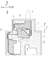
続いて、電源ユニット10の内部構成について図5、及び図7~図12を参照しながら説明する。
ケース11の内部空間にはシャーシ12が設けられ、充電端子42(図3参照)、レセプタクル搭載基板8、電源BATを含むバッテリパックBP、及びMCU搭載基板7が、ボトム部11cからトップ部11aに向かってこの順にシャーシ12に保持される。
(Internal configuration of power supply unit)
Next, the internal configuration of the power supply unit 10 will be described with reference to FIGS. 5 and 7 to 12. FIG.
A chassis 12 is provided in the inner space of the case 11, and a charging terminal 42 (see FIG. 3), a receptacle mounting board 8, a battery pack BP including a power supply BAT, and an MCU mounting board 7 extend from the bottom portion 11c to the top portion 11a. They are held by the chassis 12 in this order.
このように、ボトム部11cからトップ部11aに向かって(すなわちX方向において)、レセプタクル搭載基板8、電源BAT、及びMCU搭載基板7をこの順で並べて配置することで、電源BATとMCU搭載基板7との間にレセプタクル搭載基板8を配置した場合に比べて、電源BATに近い位置にMCU搭載基板7を配置できる。そして、電源BATに近い位置にMCU搭載基板7を配置することで、MCU搭載基板7において電源BATと接続される電子部品(例えばバッテリコネクタCn3)と電源BATとの間の配線距離を短くでき、余分な配線を減らして、電源ユニット10の小型化を図れる。併せて、電源ユニット10を製造するためのコストの削減も図れる。
In this way, by arranging the receptacle mounting board 8, the power supply BAT, and the MCU mounting board 7 in this order from the bottom part 11c toward the top part 11a (that is, in the X direction), the power supply BAT and the MCU mounting board 7, the MCU-mounted board 7 can be arranged at a position closer to the power supply BAT than when the receptacle-mounted board 8 is arranged between them. By arranging the MCU-mounted board 7 at a position close to the power supply BAT, the wiring distance between the electronic component (for example, the battery connector Cn3) connected to the power supply BAT on the MCU-mounted board 7 and the power supply BAT can be shortened. The size of the power supply unit 10 can be reduced by reducing unnecessary wiring. At the same time, the cost for manufacturing the power supply unit 10 can be reduced.
また、電源BATと接続される電子部品と電源BATとの間の配線距離が短ければ、この配線距離が長い場合に比べて、この配線を電流が流れることにより発生するノイズの影響を受ける電子部品を少なくできる。したがって、この配線を流れる電流(例えば、電源BATを充電する充電電流、又は電源BATからの放電電流)の電流値が大きくなったとしても、この電流に起因して発生するノイズが電源ユニット10の電子部品に与える影響を低減でき、電源ユニット10の動作の安定化を図れる。
In addition, if the wiring distance between the electronic components connected to the power supply BAT and the power supply BAT is short, the electronic components are more affected by the noise generated by the current flowing through the wiring than when the wiring distance is long. can be reduced. Therefore, even if the current value of the current flowing through this wiring (for example, the charging current for charging the power supply BAT or the discharging current from the power supply BAT) increases, the noise generated due to this current is The influence on electronic components can be reduced, and the operation of the power supply unit 10 can be stabilized.
また、MCU搭載基板7やバッテリパックBP等を保持するシャーシ12は、合成樹脂(例えばプラスチック)等の絶縁材料によって形成されている。そして、シャーシ12は、X方向において、MCU搭載基板7を保持する部分とバッテリパックBPを保持する部分との間に、これらを区画する壁部12aを備える。この壁部12aは、MCU搭載基板7と、バッテリパックBPの電源BATとを絶縁するスペーサとして機能し得る。
Also, the chassis 12 that holds the MCU mounting board 7, the battery pack BP, and the like is made of an insulating material such as synthetic resin (for example, plastic). The chassis 12 includes a wall portion 12a between the portion holding the MCU mounting board 7 and the portion holding the battery pack BP in the X direction. This wall portion 12a can function as a spacer that insulates the MCU mounting board 7 from the power source BAT of the battery pack BP.
このように、MCU搭載基板7とバッテリパックBPとの間に絶縁性のスペーサとして機能する壁部12aを設けることで、MCU搭載基板7と電源BATとが物理的に接触することによって短絡が発生するのを回避できる。なお、本実施形態では、MCU搭載基板7と電源BATとを絶縁するスペーサをシャーシ12の壁部12aにより構成したが、これに限らず、例えばシャーシ12とは別体に設けてもよい。
Thus, by providing the wall portion 12a functioning as an insulating spacer between the MCU mounting board 7 and the battery pack BP, a short circuit occurs due to physical contact between the MCU mounting board 7 and the power supply BAT. can be avoided. In this embodiment, the wall portion 12a of the chassis 12 constitutes the spacer that insulates the MCU mounting board 7 from the power supply BAT.
また、ケース11には、充電端子42へのアクセスを許容する前述した充電用開口43、操作部14を外部に露出させる操作用開口、及び放電端子41をトップ部11aから外部に露出させる一対の放電用開口が設けられている。
In addition, the case 11 has a charging opening 43 that allows access to the charging terminal 42, an operating opening that exposes the operating portion 14 to the outside, and a pair of openings that expose the discharging terminal 41 to the outside from the top portion 11a. A discharge aperture is provided.
(MCU搭載基板)
MCU搭載基板7には、電源ユニット10の回路構成(図6等を参照)で説明した複数の電子部品が実装されている。MCU搭載基板7は、複数の層が積層されて構成された多層基板であって、略矩形形状を有する。MCU搭載基板7は、長手方向がケース11の中心線Lの延伸方向(すなわちX方向)に沿うように、且つ、一方側の素子実装面が操作部14に対向するように配置される。
(MCU mounting board)
A plurality of electronic components described in the circuit configuration of the power supply unit 10 (see FIG. 6, etc.) are mounted on the MCU mounting board 7 . The MCU mounting board 7 is a multi-layer board configured by laminating a plurality of layers, and has a substantially rectangular shape. The MCU mounting board 7 is arranged such that its longitudinal direction is along the extending direction of the center line L of the case 11 (that is, the X direction), and that one element mounting surface faces the operating section 14 .
以下の説明では、X方向を長手方向Xと称することがあり、X方向において、トップ部11a側をX1方向、ボトム部11c側をX2方向と称する。また、MCU搭載基板7上において、長手方向Xに直交する方向を短手方向Yと称し、短手方向Yにおいて、一方側(図7の左方であって、図8、9の上方且つ図10、11の下方)をY1方向、他方側(図7の右方であって、図8、9の下方且つ図10、11の上方)をY2方向と称する。長手方向XはMCU搭載基板7の長さ方向ということもでき、短手方向YはMCU搭載基板7の幅方向ということもできる。MCU搭載基板7の中心線は、電源ユニット10(ケース11)のX方向に延びる中心線Lと一致する。なお、MCU搭載基板7の中心線は、MCU搭載基板7を長手方向Xに直交する面で切断した際のMCU搭載基板7の幅方向(短手方向)及び厚さ方向の中心点を長手方向Xに連続してつなげた線である。
In the following description, the X direction is sometimes referred to as the longitudinal direction X, and in the X direction, the top portion 11a side is referred to as the X1 direction, and the bottom portion 11c side is referred to as the X2 direction. On the MCU mounting substrate 7, the direction orthogonal to the longitudinal direction X is called a lateral direction Y, and in the lateral direction Y, one side (the left side in FIG. 7, the upper side in FIGS. 10 and 11) is referred to as the Y1 direction, and the other side (the right side in FIG. 7, the lower side in FIGS. 8 and 9 and the upper side in FIGS. 10 and 11) is referred to as the Y2 direction. The longitudinal direction X can also be called the length direction of the MCU mounting board 7 , and the lateral direction Y can also be called the width direction of the MCU mounting board 7 . The centerline of the MCU mounting board 7 coincides with the centerline L of the power supply unit 10 (case 11) extending in the X direction. The center line of the MCU mounting board 7 is the center point of the width direction (transverse direction) and thickness direction of the MCU mounting board 7 when the MCU mounting board 7 is cut along a plane orthogonal to the longitudinal direction X. It is a line connected continuously to X.
MCU搭載基板7は、図7に示すように、MCU搭載基板7の大部分を占める矩形部81と、矩形部81からX1方向に突出した突出部82と、から構成される。突出部82は、短手方向Yの両端部が切り欠かれており、突出部82のX1方向の端部がケース11のトップ部11aに対向し、突出部82が設けられていない矩形部81のX1方向の端部がケース11の低床部11bに対向する。
As shown in FIG. 7, the MCU mounting board 7 is composed of a rectangular portion 81 that occupies most of the MCU mounting board 7 and a projecting portion 82 projecting from the rectangular portion 81 in the X1 direction. Both ends of the projecting portion 82 in the lateral direction Y are notched, and the end of the projecting portion 82 in the X1 direction faces the top portion 11a of the case 11, forming a rectangular portion 81 in which the projecting portion 82 is not provided. faces the low floor portion 11 b of the case 11 .
MCU搭載基板7の操作部14側の面を主面7a、反対側の面(すなわち裏面)を副面7bとすると、MCU搭載基板7は、主面7a及び副面7bの両方に電子部品が実装される両面実装基板である。
Assuming that the surface of the MCU mounting board 7 on the operation unit 14 side is the main surface 7a and the opposite side surface (that is, the back surface) is the subsurface 7b, the MCU mounting board 7 has electronic components on both the main surface 7a and the subsurface 7b. It is a double-sided mounting board to be mounted.
主面7aの主面側表面層71a(以下、単に主面7aと称する)には、図8に示すように、バッテリコネクタCn3、MCU50、操作スイッチOPS、LED_L1、LED_L2、DC/DCコンバータ63、リアクトルRc2、コンデンサCd61、コンデンサCd62、コンデンサCd63、スイッチSw4、コンデンサCd7、バリスタVR4、正極側放電端子41a等が実装される。
As shown in FIG. 8, a battery connector Cn3, an MCU 50, an operation switch OPS, LED_L1, LED_L2, a DC/DC converter 63, a DC/DC converter 63, A reactor Rc2, a capacitor Cd61, a capacitor Cd62, a capacitor Cd63, a switch Sw4, a capacitor Cd7, a varistor VR4, a positive discharge terminal 41a, and the like are mounted.
より具体的に説明すると、主面7aの略中央には、操作部14と対向するように、ボタン式の操作スイッチOPSが実装される。これにより、ユーザは、ケース11の操作部14を介して操作スイッチOPSを押し下げることができる。また、操作スイッチOPSの近傍には、短手方向Yにおいて操作スイッチOPSを挟むようにLED_L1、LED_L2が実装される。これにより、ユーザは、LED_L1及びLED_L2から出射された光を、操作部14の周囲に設けられたLED窓13を介して視認することができる。
More specifically, a button-type operation switch OPS is mounted substantially in the center of the main surface 7a so as to face the operation unit 14. Thereby, the user can push down the operation switch OPS through the operation portion 14 of the case 11 . Further, near the operation switch OPS, LED_L1 and LED_L2 are mounted so as to sandwich the operation switch OPS in the lateral direction Y. As shown in FIG. Thereby, the user can visually recognize the light emitted from LED_L1 and LED_L2 through the LED window 13 provided around the operation unit 14 .
また、主面7aのX2方向の端部には、バッテリコネクタCn3が実装される。バッテリコネクタCn3には、電源BATを含むバッテリパックBPから延びるバッテリ接続ケーブルCb2がY2方向側から接続される(図7も参照)。
A battery connector Cn3 is mounted on the end of the main surface 7a in the X2 direction. A battery connection cable Cb2 extending from a battery pack BP including a power supply BAT is connected to the battery connector Cn3 from the Y2 direction side (see also FIG. 7).
ここで、バッテリコネクタCn3が実装されるX2方向の端部は、電源BATに近い位置である。このように、電源BATに近い位置にバッテリコネクタCn3を配置することで、バッテリ接続ケーブルCb2を短く構成することが可能となり、電源ユニット10の小型化を図れる。併せて、電源ユニット10を製造するためのコストの削減も図れる。また、バッテリ接続ケーブルCb2を短くすることで、電源BATを充電する充電電流あるいは電源BATからの放電電流等のバッテリ接続ケーブルCb2を流れる電流の電流値が大きくなったとしても、この電流に起因して発生するノイズが電源ユニット10の電子部品に与える影響を低減でき、電源ユニット10の動作の安定化も図れる。
Here, the end in the X2 direction where the battery connector Cn3 is mounted is located near the power source BAT. By arranging the battery connector Cn3 at a position close to the power supply BAT in this manner, the battery connection cable Cb2 can be shortened, and the size of the power supply unit 10 can be reduced. At the same time, the cost for manufacturing the power supply unit 10 can be reduced. In addition, even if the current value of the current flowing through the battery connection cable Cb2, such as the charging current for charging the power supply BAT or the discharging current from the power supply BAT, increases due to the shortening of the battery connection cable Cb2, it is caused by this current. Therefore, the influence of noise generated in the power supply unit 10 on the electronic components of the power supply unit 10 can be reduced, and the operation of the power supply unit 10 can be stabilized.
ところで、前述したように、長手方向Xにおいて、MCU搭載基板7とバッテリパックBP(すなわち電源BAT)との間には、これらを絶縁するスペーサである壁部12aが設けられている。このため、本実施形態では、バッテリコネクタCn3をY2方向に向けた状態でMCU搭載基板7に実装するとともに、バッテリ接続ケーブルCb2をY2方向側からバッテリコネクタCn3に接続している。これにより、バッテリ接続ケーブルCb2及び/又は壁部12aを複雑な形状とすることなく、これらが物理的に干渉するのを回避することが可能となる。
By the way, as described above, between the MCU mounting board 7 and the battery pack BP (that is, the power source BAT) in the longitudinal direction X, the wall portion 12a, which is a spacer for insulating them, is provided. Therefore, in this embodiment, the battery connector Cn3 is mounted on the MCU mounting board 7 with the battery connector Cn3 directed in the Y2 direction, and the battery connection cable Cb2 is connected to the battery connector Cn3 from the Y2 direction side. This makes it possible to avoid physical interference between the battery connection cable Cb2 and/or the wall portion 12a without making them complicated in shape.
なお、本実施形態では、バッテリコネクタCn3をY2方向に向けた状態でMCU搭載基板7に実装するとともに、バッテリ接続ケーブルCb2をY2方向側からバッテリコネクタCn3に接続するようにしたが、これに限らない。バッテリコネクタCn3をY1方向に向けた状態でMCU搭載基板7に実装するとともに、バッテリ接続ケーブルCb2をY1方向側からバッテリコネクタCn3に接続するようにしてもよい。
In this embodiment, the battery connector Cn3 is mounted on the MCU mounting board 7 with the battery connector Cn3 directed in the Y2 direction, and the battery connection cable Cb2 is connected to the battery connector Cn3 from the Y2 direction side. Absent. The battery connector Cn3 may be mounted on the MCU mounting board 7 with the battery connector Cn3 directed in the Y1 direction, and the battery connection cable Cb2 may be connected to the battery connector Cn3 from the Y1 direction side.
また、図8において、符号55で示す破線は、主面7aの裏面である副面7bに実装される充電IC55の実装位置をあらわしている。すなわち、バッテリコネクタCn3及び充電IC55は、バッテリコネクタCn3の少なくとも一部が、MCU搭載基板7と直交する方向において充電IC55と重なるように、それぞれMCU搭載基板7の異なる面に実装されている。ここで、MCU搭載基板7と直交する方向とは、長手方向X及び短手方向Yと直交する方向を指すものとする。
Also, in FIG. 8, the dashed line indicated by reference numeral 55 represents the mounting position of the charging IC 55 mounted on the subsurface 7b, which is the back surface of the main surface 7a. That is, the battery connector Cn3 and the charging IC 55 are mounted on different surfaces of the MCU mounting board 7 so that at least part of the battery connector Cn3 overlaps the charging IC 55 in the direction orthogonal to the MCU mounting board 7 . Here, the direction orthogonal to the MCU mounting board 7 refers to the direction orthogonal to the longitudinal direction X and the lateral direction Y. As shown in FIG.
バッテリコネクタCn3及び充電IC55は物理的なサイズが大きく、MCU搭載基板7上で大きな面積を占有しやすい。そこで、バッテリコネクタCn3及び充電IC55をMCU搭載基板7の異なる面にそれぞれ実装することで、主面7a及び副面7bの両面を有効活用してバッテリコネクタCn3及び充電IC55を実装することが可能となる。これにより、MCU搭載基板7が大型化するのを回避しながら、バッテリコネクタCn3及び充電IC55をMCU搭載基板7に実装できる。
The physical size of the battery connector Cn3 and charging IC 55 is large and tends to occupy a large area on the MCU mounting board 7. Therefore, by mounting the battery connector Cn3 and the charging IC 55 on different surfaces of the MCU mounting substrate 7, both the main surface 7a and the subsurface 7b can be effectively used to mount the battery connector Cn3 and the charging IC 55. Become. As a result, the battery connector Cn3 and the charging IC 55 can be mounted on the MCU mounting board 7 while avoiding the MCU mounting board 7 from increasing in size.
そして、バッテリコネクタCn3の少なくとも一部が、MCU搭載基板7の主面7aと直交する方向において充電IC55と重なるようにすることで、バッテリコネクタCn3と充電IC55との間の配線距離を短くできる。これにより、余分な配線(例えばMCU搭載基板7に形成される導電パターン)を減らして、MCU搭載基板7の小型化を図れる。併せて、MCU搭載基板7を製造するためのコストの削減も図れる。また、バッテリコネクタCn3と充電IC55との間の配線距離が短ければ、この配線(例えばVBATラインLn2)を流れる電流の電流値が大きくなったとしても、この電流に起因して発生するノイズがMCU搭載基板7における他の電子部品に与える影響を低減でき、電源ユニット10の動作の安定化を図れる。バッテリコネクタCn3と充電IC55との間の配線を流れる電流は、例えば、電源BATを充電する充電電流(以下、単に充電電流とも称する)や、電源BATからの放電電流(以下、単に放電電流とも称する)である。
At least part of the battery connector Cn3 overlaps the charging IC 55 in the direction orthogonal to the main surface 7a of the MCU mounting board 7, so that the wiring distance between the battery connector Cn3 and the charging IC 55 can be shortened. As a result, unnecessary wiring (for example, conductive patterns formed on the MCU mounting board 7) can be reduced, and the MCU mounting board 7 can be miniaturized. At the same time, the cost for manufacturing the MCU mounting board 7 can be reduced. Also, if the wiring distance between the battery connector Cn3 and the charging IC 55 is short, even if the current value of the current flowing through this wiring (for example, the VBAT line Ln2) is large, the noise generated due to this current will not affect the MCU. The influence of the mounting board 7 on other electronic components can be reduced, and the operation of the power supply unit 10 can be stabilized. The current flowing through the wiring between the battery connector Cn3 and the charging IC 55 is, for example, a charging current for charging the power supply BAT (hereinafter simply referred to as charging current) or a discharging current from the power supply BAT (hereinafter simply referred to as discharging current). ).
また、主面7aのX1方向の端部である突出部82には、正極側放電端子41aが実装される。正極側放電端子41aには、第1カートリッジ20に設けられたヒータ21が接続される。正極側放電端子41aが実装されるX1方向の端部は、第1カートリッジ20に近い位置である。このように、第1カートリッジ20に近い位置に正極側放電端子41aを配置することで、正極側放電端子41aとヒータ21とを容易且つ効率的に接続することが可能となる。
Also, the positive electrode side discharge terminal 41a is mounted on the projecting portion 82, which is the end portion of the main surface 7a in the X1 direction. A heater 21 provided in the first cartridge 20 is connected to the positive discharge terminal 41a. The end in the X1 direction where the positive discharge terminal 41 a is mounted is located near the first cartridge 20 . By arranging the positive electrode side discharge terminal 41a at a position close to the first cartridge 20 in this manner, the positive electrode side discharge terminal 41a and the heater 21 can be easily and efficiently connected.
また、正極側放電端子41aは、突出部82において中心線Lを挟んでY2方向側に配置される。一方、突出部82において中心線Lを挟んでY1方向側には、スイッチSw4が配置される。
In addition, the positive electrode side discharge terminal 41a is arranged on the Y2 direction side of the center line L in the protruding portion 82 . On the other hand, a switch Sw4 is arranged on the Y1 direction side of the projecting portion 82 with the center line L interposed therebetween.
また、主面7aには、X方向において、操作スイッチOPSとスイッチSw4との間に、DC/DCコンバータ63、リアクトルRc2、コンデンサCd61、コンデンサCd62、コンデンサCd63、コンデンサCd7等が実装されている。
A DC/DC converter 63, a reactor Rc2, a capacitor Cd61, a capacitor Cd62, a capacitor Cd63, a capacitor Cd7, etc. are mounted on the main surface 7a between the operation switch OPS and the switch Sw4 in the X direction.
DC/DCコンバータ63、コンデンサCd61、コンデンサCd62、及びコンデンサCd63は、図8に示すように、MCU搭載基板7と直交する方向から見て(以下、MCU搭載基板7の平面視ともいう)、略L字状に配置されている。
As shown in FIG. 8, the DC/DC converter 63, the capacitor Cd61, the capacitor Cd62, and the capacitor Cd63 are approximately They are arranged in an L shape.
より具体的に説明すると、コンデンサCd61は、短手方向Y(すなわちMCU搭載基板7の幅方向)において、DC/DCコンバータ63及びコンデンサCd62と一列に並ぶ一方で、コンデンサCd63とは一列に並ばない。ここで、短手方向Yにおいて一列に並ぶとは、短手方向Yから見て、それぞれの少なくとも一部が重なることをいう。
More specifically, the capacitor Cd61 is aligned with the DC/DC converter 63 and the capacitor Cd62 in the lateral direction Y (that is, the width direction of the MCU mounting board 7), but is not aligned with the capacitor Cd63. . Here, lining up in the transverse direction Y means that at least a part of each overlaps when viewed from the transverse direction Y. As shown in FIG.
また、コンデンサCd63は、長手方向X(すなわちMCU搭載基板7の長さ方向)において、DC/DCコンバータ63と一列に並ぶ一方で、コンデンサCd61及びコンデンサCd62とは一列に並ばない。ここで、長手方向Xにおいて一列に並ぶとは、長手方向Xから見て、それぞれの少なくとも一部が重なることをいう。
Also, the capacitor Cd63 is aligned with the DC/DC converter 63 in the longitudinal direction X (that is, the length direction of the MCU mounting board 7), but is not aligned with the capacitors Cd61 and Cd62. Here, lining up in the longitudinal direction X means that at least a part of each overlaps when viewed from the longitudinal direction X.
すなわち、コンデンサCd61及びコンデンサCd63は、図8に示すように、MCU搭載基板7の長さ方向である長手方向X、及びMCU搭載基板7の幅方向である短手方向Yにおいて一列に並ばない。同様に、コンデンサCd62及びコンデンサCd63は、長手方向X及び短手方向Yにおいて一列に並ばない。
That is, the capacitors Cd61 and Cd63 are not aligned in the longitudinal direction X, which is the length direction of the MCU mounting board 7, and the lateral direction Y, which is the width direction of the MCU mounting board 7, as shown in FIG. Similarly, the capacitors Cd62 and Cd63 are not aligned in the longitudinal direction X and the lateral direction Y.
仮に、コンデンサCd61又はコンデンサCd62と、コンデンサCd63とを、長手方向X又は短手方向Yにおいて一列に並べてMCU搭載基板7に実装すると、これらを並べるスペースを確保するために、MCU搭載基板7の長手方向Xにおける大きさ(すなわち長さ方向における大きさ。以下、長さ寸法とも称する)、又は短手方向Yにおける大きさ(すなわち幅方向における大きさ。以下、幅寸法とも称する)が大きくなるおそれがある。
If the capacitor Cd61 or the capacitor Cd62 and the capacitor Cd63 are arranged in a line in the longitudinal direction X or the transverse direction Y and mounted on the MCU mounting board 7, the longitudinal direction of the MCU mounting board 7 is required to secure space for arranging them. The size in the direction X (that is, the size in the length direction; hereinafter also referred to as the length dimension) or the size in the lateral direction Y (that is, the size in the width direction; hereinafter also referred to as the width dimension) may increase. There is
そこで、本実施形態では、コンデンサCd61又はコンデンサCd62と、コンデンサCd63とを、長手方向X及び短手方向Yにおいて一列に並ばないようにMCU搭載基板7に実装することで、これらを一列に並べるようにした場合に比べて、MCU搭載基板7の長さ寸法及び幅寸法が大きくなるのを回避している。これにより、MCU搭載基板7を小型化でき、MCU搭載基板7を製造するためのコストの削減を図れる。また、MCU搭載基板7を小型化することで、電源ユニット10自体を小型化することも可能となる。これにより、エアロゾル吸引器1の可搬性を向上させて、ユーザの利便性の向上を図れる。
Therefore, in this embodiment, the capacitor Cd61 or the capacitor Cd62 and the capacitor Cd63 are mounted on the MCU mounting board 7 so as not to be aligned in the longitudinal direction X and the lateral direction Y, so that they are aligned in a line. This prevents the MCU mounting board 7 from increasing in length and width as compared with the case of . As a result, the MCU mounting board 7 can be miniaturized, and the cost for manufacturing the MCU mounting board 7 can be reduced. Further, by miniaturizing the MCU mounting board 7, it is also possible to miniaturize the power supply unit 10 itself. Thereby, the portability of the aerosol inhaler 1 can be improved, and the user's convenience can be improved.
また、本実施形態では、長手方向XにおいてDC/DCコンバータ63と一列に並ぶようにMCU搭載基板7に実装されるコンデンサの数は、1つ(コンデンサCd63のみ)であり、短手方向YにおいてDC/DCコンバータ63と一列に並ぶようにMCU搭載基板7に実装されるコンデンサの数(コンデンサCd61及びコンデンサCd62の2つ)よりも少なくなっている。このように、長手方向XにおいてDC/DCコンバータ63と一列に並ぶようにMCU搭載基板7に実装されるコンデンサの数を、短手方向YにおいてDC/DCコンバータ63と一列に並ぶようにMCU搭載基板7に実装されるコンデンサの数よりも少なくすることで、MCU搭載基板7の長さ寸法が大きくなるのを回避でき、MCU搭載基板7の小型化を図れる。
Further, in the present embodiment, the number of capacitors mounted on the MCU mounting board 7 so as to be aligned in the longitudinal direction X with the DC/DC converter 63 is one (only the capacitor Cd63). It is smaller than the number of capacitors (two capacitors Cd61 and Cd62) mounted on the MCU mounting board 7 so as to be aligned with the DC/DC converter 63 in a line. In this way, the number of capacitors mounted on the MCU-mounted board 7 so as to line up with the DC/DC converter 63 in the longitudinal direction X is reduced to the number of capacitors mounted on the MCU mounted in line with the DC/DC converter 63 in the lateral direction Y. By making the number of capacitors smaller than the number of capacitors mounted on the board 7, it is possible to prevent the length dimension of the MCU-mounted board 7 from becoming large, and to reduce the size of the MCU-mounted board 7. - 特許庁
ところで、前述したように、コンデンサCd63の静電容量は、コンデンサCd61の静電容量よりも大きいものとなっている。このように、静電容量が大きく物理的なサイズも大きくなりがちなコンデンサCd63を長手方向XにおいてDC/DCコンバータ63と並べることで、これらを短手方向Yに並べるようにした場合に比べて、MCU搭載基板7の幅寸法が大きくなるのを回避できる。したがって、MCU搭載基板7の小型化を図れる。
By the way, as described above, the capacitance of the capacitor Cd63 is larger than that of the capacitor Cd61. In this way, by arranging the capacitor Cd 63, which tends to have a large capacitance and a large physical size, in the longitudinal direction X with the DC/DC converter 63, compared to the case where they are arranged in the lateral direction Y , the width dimension of the MCU mounting board 7 can be prevented from becoming large. Therefore, the size of the MCU mounting board 7 can be reduced.
さらに、前述したように、コンデンサCd62の静電容量も、コンデンサCd61の静電容量よりも大きいものとなっている。このように、静電容量が大きく物理的なサイズも大きくなりがちなコンデンサCd62を短手方向YにおいてDC/DCコンバータ63と並べることで、コンデンサCd62及びコンデンサCd63が短手方向Yに並ぶことを回避できる。これにより、コンデンサCd62及びコンデンサCd63を短手方向Yに並べるようにした場合に比べて、MCU搭載基板7の幅寸法が大きくなるのを回避できる。したがって、MCU搭載基板7の小型化を図れる。
Furthermore, as described above, the capacitance of the capacitor Cd62 is also larger than that of the capacitor Cd61. In this way, by arranging the capacitor Cd62, which tends to have a large capacitance and a large physical size, with the DC/DC converter 63 in the lateral direction Y, it is possible to realize that the capacitors Cd62 and Cd63 are aligned in the lateral direction Y. can be avoided. As a result, compared to the case where the capacitors Cd62 and Cd63 are arranged in the lateral direction Y, it is possible to avoid increasing the width dimension of the MCU mounting board 7 . Therefore, the size of the MCU mounting board 7 can be reduced.
また、DC/DCコンバータ63、コンデンサCd61、及びコンデンサCd62は、短手方向Yにおいてこの順で一列に並ぶ。すなわち、MCU搭載基板7において、DC/DCコンバータ63の周辺には、多数のビア等が設けられる傾向がある。このため、コンデンサCd62といったサイズが大きい大容量のコンデンサを、MCU搭載基板7において、DC/DCコンバータ63に近接して実装するのは難しい。一方、コンデンサCd61といったサイズの小さいコンデンサであれば、MCU搭載基板7において、DC/DCコンバータ63に近接して実装しやすい。したがって、DC/DCコンバータ63、コンデンサCd61、及びコンデンサCd62を、短手方向Yにおいてこの順で並べることにより、これらを高密度でMCU搭載基板7に実装することを可能にし、MCU搭載基板7の基板面積を有効活用して、MCU搭載基板7の小型化を図れる。
Also, the DC/DC converter 63, the capacitor Cd61, and the capacitor Cd62 are arranged in a line in this order in the transverse direction Y. That is, in the MCU mounting board 7, there tends to be a large number of vias and the like provided around the DC/DC converter 63. FIG. Therefore, it is difficult to mount a large-sized, large-capacity capacitor, such as the capacitor Cd 62 , close to the DC/DC converter 63 on the MCU mounting board 7 . On the other hand, a small-sized capacitor such as the capacitor Cd61 can be easily mounted on the MCU mounting board 7 in the vicinity of the DC/DC converter 63 . Therefore, by arranging the DC/DC converter 63, the capacitor Cd61, and the capacitor Cd62 in this order in the lateral direction Y, it is possible to mount them on the MCU mounting board 7 at high density. By effectively utilizing the board area, the MCU mounting board 7 can be miniaturized.
また、コンデンサCd63は、MCU搭載基板7の平面視で、長辺と短辺からなる長方形形状を有する。そして、コンデンサCd63は、その短辺が長手方向Xに対して平行となるように、MCU搭載基板7に実装されている。換言すると、コンデンサCd63は、コンデンサCd63の短手方向がMCU搭載基板7の長手方向Xと一致するように、MCU搭載基板7に実装されている。これにより、コンデンサCd63をDC/DCコンバータ63と長手方向Xに並べても、MCU搭載基板7の長さ寸法が増加するのを抑制できる。したがって、MCU搭載基板7の小型化を図れる。
Also, the capacitor Cd63 has a rectangular shape with long sides and short sides in a plan view of the MCU mounting board 7 . The capacitor Cd63 is mounted on the MCU mounting board 7 so that its short sides are parallel to the longitudinal direction X. As shown in FIG. In other words, the capacitor Cd63 is mounted on the MCU mounting board 7 such that the short direction of the capacitor Cd63 is aligned with the longitudinal direction X of the MCU mounting board 7 . Thus, even if the capacitor Cd 63 and the DC/DC converter 63 are arranged in the longitudinal direction X, an increase in the length dimension of the MCU mounting board 7 can be suppressed. Therefore, the size of the MCU mounting board 7 can be reduced.
また、コンデンサCd62は、MCU搭載基板7の平面視で、長辺と短辺からなる長方形形状を有する。そして、コンデンサCd62は、その長辺が長手方向Xに対して平行となるように、MCU搭載基板7に実装されている。換言すると、コンデンサCd62は、コンデンサCd62の短手方向がMCU搭載基板7の短手方向Yと一致するように、MCU搭載基板7に実装されている。これにより、コンデンサCd62をDC/DCコンバータ63と短手方向Yに並べても、MCU搭載基板7の幅寸法が増加するのを抑制できる。したがって、MCU搭載基板7の小型化を図れる。
Also, the capacitor Cd62 has a rectangular shape with long sides and short sides in a plan view of the MCU mounting board 7 . The capacitor Cd62 is mounted on the MCU mounting board 7 so that its long sides are parallel to the longitudinal direction X. As shown in FIG. In other words, the capacitor Cd62 is mounted on the MCU mounting board 7 so that the short side direction of the capacitor Cd62 is aligned with the short side direction Y of the MCU mounting board 7 . Accordingly, even if the capacitor Cd 62 and the DC/DC converter 63 are arranged in the lateral direction Y, an increase in the width dimension of the MCU mounting board 7 can be suppressed. Therefore, the size of the MCU mounting board 7 can be reduced.
副面7bの副面側表面層71b(以下、単に副面7bと称する)には、図10に示すように、充電IC55、リアクトルRc1、保護IC61、MCU搭載基板側コネクタCn2、吸引センサ15、負極側放電端子41b等が実装される。
As shown in FIG. 10, a charging IC 55, a reactor Rc1, a protection IC 61, an MCU mounting board side connector Cn2, a suction sensor 15, A negative electrode side discharge terminal 41b and the like are mounted.
より具体的に説明すると、副面7bの略中央には、MCU搭載基板側コネクタCn2が実装される。MCU搭載基板側コネクタCn2の実装位置について詳述すると、図10中の符号O1は、MCU搭載基板7と直交する方向から見たMCU搭載基板7の中心をあらわしている。ここで、MCU搭載基板7の中心O1は、ケース11の中心線Lと一致するMCU搭載基板7の中心線上で、且つ長手方向XにおけるMCU搭載基板7の中央となる点である。
More specifically, the MCU mounting board side connector Cn2 is mounted approximately in the center of the secondary surface 7b. 10 indicates the center of the MCU mounting board 7 viewed from a direction orthogonal to the MCU mounting board 7. In FIG. Here, the center O1 of the MCU mounting board 7 is the center of the MCU mounting board 7 in the longitudinal direction X, on the center line of the MCU mounting board 7 that coincides with the center line L of the case 11 .
また、図10中の符号O2は、MCU搭載基板7と直交する方向から見たMCU搭載基板側コネクタCn2の中心をあらわしている。ここで、MCU搭載基板側コネクタCn2は、MCU搭載基板7の平面視で、2辺が長手方向Xに平行で且つ他の2辺が短手方向Yに平行な略矩形形状を有する。このため、MCU搭載基板側コネクタCn2の中心O2は、長手方向XにおけるMCU搭載基板側コネクタCn2の中央で、且つ短手方向YにおけるMCU搭載基板側コネクタCn2の中央となる点となる。
Reference O2 in FIG. 10 represents the center of the MCU mounting board side connector Cn2 as seen from the direction orthogonal to the MCU mounting board 7 . Here, the MCU mounting board side connector Cn2 has a substantially rectangular shape in which two sides are parallel to the longitudinal direction X and the other two sides are parallel to the lateral direction Y in a plan view of the MCU mounting board 7 . Therefore, the center O2 of the MCU mounting board side connector Cn2 is the center of the MCU mounting board side connector Cn2 in the longitudinal direction X and the center of the MCU mounting board side connector Cn2 in the lateral direction Y.
そして、本実施形態では、MCU搭載基板側コネクタCn2に最も近いMCU搭載基板7の縁とMCU搭載基板側コネクタCn2の中心O2との間の最短距離d1が、MCU搭載基板7の中心O1とMCU搭載基板側コネクタCn2の中心O2との間の最短距離d2よりも長くなるように、MCU搭載基板側コネクタCn2をMCU搭載基板7の副面7bに実装している。
In this embodiment, the shortest distance d1 between the edge of the MCU mounting board 7 closest to the MCU mounting board side connector Cn2 and the center O2 of the MCU mounting board side connector Cn2 is the distance between the center O1 of the MCU mounting board 7 and the MCU. The MCU mounting board side connector Cn2 is mounted on the secondary surface 7b of the MCU mounting board 7 so as to be longer than the shortest distance d2 to the center O2 of the mounting board side connector Cn2.
このように、MCU搭載基板側コネクタCn2に最も近いMCU搭載基板7の縁とMCU搭載基板側コネクタCn2との間の最短距離d1が、MCU搭載基板7の中心とMCU搭載基板側コネクタCn2との間の最短距離d2よりも長くなるように、MCU搭載基板側コネクタCn2をMCU搭載基板7に実装することで、MCU搭載基板7(ここでは副面7b)の略中央にMCU搭載基板側コネクタCn2を実装できる。
Thus, the shortest distance d1 between the edge of the MCU mounting board 7 closest to the MCU mounting board side connector Cn2 and the MCU mounting board side connector Cn2 is the distance between the center of the MCU mounting board 7 and the MCU mounting board side connector Cn2. By mounting the MCU mounting board side connector Cn2 on the MCU mounting board 7 so as to be longer than the shortest distance d2 between can be implemented.
そして、MCU搭載基板7の略中央にMCU搭載基板側コネクタCn2を実装することで、MCU搭載基板7の端部にMCU搭載基板側コネクタCn2を実装した場合に比べて、MCU搭載基板側コネクタCn2とMCU搭載基板7に実装される他の電子部品との間の配線距離を短くすることが可能となる。これは、MCU搭載基板側コネクタCn2の周囲且つ近傍に多くの電子部品を実装しやすくなるためである。これにより、MCU搭載基板側コネクタCn2とMCU搭載基板7に実装される他の電子部品とを接続するための配線としてMCU搭載基板7に形成される導電パターンを短くできる。したがって、余分な導電パターンを減らして、MCU搭載基板7の小型化を図れる。併せて、MCU搭載基板7を製造するためのコストの削減も図れる。
By mounting the MCU mounting board-side connector Cn2 approximately in the center of the MCU mounting board 7, compared to the case where the MCU mounting board-side connector Cn2 is mounted at the end of the MCU mounting board 7, the MCU mounting board-side connector Cn2 and other electronic components mounted on the MCU mounting board 7 can be shortened. This is because many electronic components can be easily mounted around and in the vicinity of the MCU mounting board side connector Cn2. As a result, the conductive pattern formed on the MCU mounting board 7 as wiring for connecting the MCU mounting board side connector Cn2 and other electronic components mounted on the MCU mounting board 7 can be shortened. Therefore, it is possible to reduce the size of the MCU mounting board 7 by reducing redundant conductive patterns. At the same time, the cost for manufacturing the MCU mounting board 7 can be reduced.
また、MCU搭載基板側コネクタCn2には、充電端子42等を実装したレセプタクル搭載基板8から延びる基板接続ケーブルCb1が接続される。より具体的に説明すると、本実施形態では、MCU搭載基板側コネクタCn2をY1方向に向けた状態でMCU搭載基板7に実装するとともに、基板接続ケーブルCb1をY1方向側からMCU搭載基板側コネクタCn2に接続している。
Also, a board connection cable Cb1 extending from the receptacle mounting board 8 on which the charging terminal 42 and the like are mounted is connected to the MCU mounting board side connector Cn2. More specifically, in this embodiment, the MCU mounting board side connector Cn2 is mounted on the MCU mounting board 7 with the MCU mounting board side connector Cn2 directed in the Y1 direction, and the board connection cable Cb1 is connected to the MCU mounting board side connector Cn2 from the Y1 direction side. connected to.
このように、基板接続ケーブルCb1をMCU搭載基板7の短手方向YからMCU搭載基板側コネクタCn2に接続することで、MCU搭載基板7の略中央にMCU搭載基板側コネクタCn2を実装しても、MCU搭載基板7に実装される他の電子部品と基板接続ケーブルCb1とが物理的に干渉しにくくすることができる。したがって、MCU搭載基板7に実装される他の電子部品の耐久性を向上させたり、MCU搭載基板7における各電子部品のレイアウトの自由度を向上させたりすることが可能となる。
In this way, by connecting the board connection cable Cb1 to the MCU mounting board side connector Cn2 from the lateral direction Y of the MCU mounting board 7, the MCU mounting board side connector Cn2 can be mounted substantially in the center of the MCU mounting board 7. , physical interference between other electronic components mounted on the MCU mounting board 7 and the board connection cable Cb1 can be made difficult. Therefore, it is possible to improve the durability of other electronic components mounted on the MCU mounting board 7 and improve the degree of freedom in layout of each electronic component on the MCU mounting board 7 .
一方、仮に、MCU搭載基板7の略中央にMCU搭載基板側コネクタCn2を実装して、基板接続ケーブルCb1をMCU搭載基板7の長手方向XからMCU搭載基板側コネクタCn2に接続するようにすると、長手方向XにおいてMCU搭載基板側コネクタCn2と一列に並ぶ電子部品には、基板接続ケーブルCb1との物理的な干渉を回避する観点から、背の高い電子部品を用いることができない等の制約が生じ得る。
On the other hand, if the MCU mounting board side connector Cn2 is mounted approximately in the center of the MCU mounting board 7 and the board connection cable Cb1 is connected to the MCU mounting board side connector Cn2 from the longitudinal direction X of the MCU mounting board 7, The electronic components aligned in the longitudinal direction X with the MCU-mounted board-side connector Cn2 are restricted from the standpoint of avoiding physical interference with the board connection cable Cb1, such as not being able to use tall electronic components. obtain.
なお、本実施形態では、MCU搭載基板側コネクタCn2をY1方向に向けた状態でMCU搭載基板7に実装するとともに、基板接続ケーブルCb1をY1方向側からMCU搭載基板側コネクタCn2に接続するようにしたが、これに限らない。MCU搭載基板側コネクタCn2をY2方向に向けた状態でMCU搭載基板7に実装するとともに、基板接続ケーブルCb1をY2方向側からMCU搭載基板側コネクタCn2に接続するようにしてもよい。
In this embodiment, the MCU mounting board side connector Cn2 is mounted in the direction Y1, and the board connection cable Cb1 is connected to the MCU mounting board side connector Cn2 from the Y1 direction side. However, it is not limited to this. The MCU mounting board side connector Cn2 may be mounted on the MCU mounting board 7 with the MCU mounting board side connector Cn2 directed in the Y2 direction, and the board connection cable Cb1 may be connected to the MCU mounting board side connector Cn2 from the Y2 direction side.
また、副面7bには、MCU搭載基板側コネクタCn2のX2方向側に充電IC55が実装される。これにより、主面7aのX2方向の端部に実装されるバッテリコネクタCn3に近い位置に充電IC55を配置できる。そして、前述したように、バッテリコネクタCn3の少なくとも一部が、MCU搭載基板7の主面7aと直交する方向において充電IC55と重なるようにすることが可能となる。
Also, on the secondary surface 7b, a charging IC 55 is mounted on the X2 direction side of the MCU mounting board side connector Cn2. Thereby, the charging IC 55 can be arranged at a position close to the battery connector Cn3 mounted on the end of the main surface 7a in the X2 direction. Then, as described above, at least part of the battery connector Cn3 can overlap the charging IC 55 in the direction orthogonal to the main surface 7a of the MCU mounting board 7. FIG.
さらに、副面7bには、長手方向Xにおいて充電IC55とMCU搭載基板側コネクタCn2との間であって、短手方向YにおけるY1方向寄りにはリアクトルRc1が実装され、Y2方向寄りには保護IC61が実装される。
Further, on the secondary surface 7b, between the charging IC 55 and the MCU mounting board side connector Cn2 in the longitudinal direction X, a reactor Rc1 is mounted near the Y1 direction in the lateral direction Y, and a reactor Rc1 is mounted near the Y2 direction. IC 61 is mounted.
また、副面7bには、MCU搭載基板側コネクタCn2のX1方向側に吸引センサ15が実装される。これにより、電源ユニット10では、X2方向からX1方向に向かって、MCU搭載基板7に対しX2方向側に配置されるレセプタクル搭載基板8(図7参照)、MCU搭載基板側コネクタCn2、及び吸引センサ15がこの順で並ぶ。換言すると、吸引センサ15は、長手方向Xにおいて、MCU搭載基板7に対しX2方向側に配置されるレセプタクル搭載基板8と、MCU搭載基板側コネクタCn2との間に配置されていない。
Also, on the secondary surface 7b, a suction sensor 15 is mounted on the X1 direction side of the MCU mounting board side connector Cn2. As a result, in the power supply unit 10, from the X2 direction to the X1 direction, the receptacle mounting board 8 (see FIG. 7) arranged on the X2 direction side with respect to the MCU mounting board 7, the MCU mounting board side connector Cn2, and the suction sensor 15 are arranged in this order. In other words, the suction sensor 15 is not arranged in the longitudinal direction X between the receptacle mounting board 8 arranged on the X2 direction side with respect to the MCU mounting board 7 and the MCU mounting board side connector Cn2.
ここで、吸引センサ15は、副面7b(副面側表面層71b)からの高さがMCU搭載基板側コネクタCn2よりも高い電子部品となっている。内部に設けられたダイアフラムの振動等により吸引を検知するという構造上、吸引センサ15は大型化しやすいためである。仮に、このような吸引センサ15を、MCU搭載基板7においてMCU搭載基板側コネクタCn2のX2方向側(すなわちレセプタクル搭載基板8とMCU搭載基板側コネクタCn2との間)に配置すると、MCU搭載基板側コネクタCn2に接続される基板接続ケーブルCb1と吸引センサ15とが物理的に干渉しやすくなる。そして、この干渉を回避するために、基板接続ケーブルCb1を複雑な形状とせざるを得なくなったりする。
Here, the suction sensor 15 is an electronic component whose height from the secondary surface 7b (subsurface side surface layer 71b) is higher than the MCU mounting board side connector Cn2. This is because the suction sensor 15 tends to be large due to its structure in which suction is detected by vibration of a diaphragm provided inside. If such a suction sensor 15 is arranged on the MCU mounting board 7 on the X2 direction side of the MCU mounting board side connector Cn2 (that is, between the receptacle mounting board 8 and the MCU mounting board side connector Cn2), the MCU mounting board side The substrate connection cable Cb1 connected to the connector Cn2 and the suction sensor 15 are likely to physically interfere with each other. In order to avoid this interference, the board connection cable Cb1 has no choice but to have a complicated shape.
そこで、本実施形態では、吸引センサ15を、MCU搭載基板7においてMCU搭載基板側コネクタCn2のX1方向側(すなわちレセプタクル搭載基板8の反対側)に配置した。これにより、基板接続ケーブルCb1を複雑な形状とすることなく、基板接続ケーブルCb1と吸引センサ15とが物理的に干渉するのを容易に回避することが可能となる。したがって、基板接続ケーブルCb1が複雑な形状となることによる電源ユニット10の製造コストの増加を抑制できる。
Therefore, in this embodiment, the suction sensor 15 is arranged on the MCU mounting board 7 on the X1 direction side of the MCU mounting board side connector Cn2 (that is, on the opposite side of the receptacle mounting board 8). This makes it possible to easily avoid physical interference between the board connection cable Cb1 and the suction sensor 15 without making the board connection cable Cb1 have a complicated shape. Therefore, it is possible to suppress an increase in the manufacturing cost of the power supply unit 10 due to the complicated shape of the board connection cable Cb1.
また、本実施形態では、リアクトルRc2及び操作スイッチOPSが、吸引センサ15と同様にMCU搭載基板側コネクタCn2よりも背の高い電子部品(すなわちMCU搭載基板7における実装面からの高さが高い電子部品)となっている。そこで、本実施形態では、前述したように、リアクトルRc2及び操作スイッチOPSについては主面7aに実装することで、基板接続ケーブルCb1を複雑な形状とすることなく、これらの電子部品と基板接続ケーブルCb1とが物理的に干渉しにくくなるようにしている。
In addition, in the present embodiment, the reactor Rc2 and the operation switch OPS are, like the suction sensor 15, an electronic component taller than the MCU mounting board side connector Cn2 (that is, an electronic component having a higher height from the mounting surface of the MCU mounting board 7). parts). Therefore, in the present embodiment, as described above, the reactor Rc2 and the operation switch OPS are mounted on the main surface 7a. Cb1 is made to be physically less likely to interfere.
また、本実施形態では、前述したように、バッテリコネクタCn3は主面7a、MCU搭載基板側コネクタCn2は副面7bといったように、これらのコネクタをMCU搭載基板7の異なる面にそれぞれ実装している。バッテリコネクタCn3及びMCU搭載基板側コネクタCn2は物理的なサイズが大きく、MCU搭載基板7上で大きな面積を占有しやすい。そこで、バッテリコネクタCn3及びMCU搭載基板側コネクタCn2をMCU搭載基板7の異なる面にそれぞれ実装することで、主面7a及び副面7bの両面を有効活用してバッテリコネクタCn3及びMCU搭載基板側コネクタCn2を実装することが可能となる。これにより、MCU搭載基板7が大型化するのを回避しながら、バッテリコネクタCn3及びMCU搭載基板側コネクタCn2をMCU搭載基板7に実装できる。
In this embodiment, as described above, the battery connector Cn3 is mounted on the main surface 7a, and the MCU mounting board side connector Cn2 is mounted on the subsurface 7b. there is The battery connector Cn3 and the MCU-mounted board-side connector Cn2 are physically large in size and tend to occupy a large area on the MCU-mounted board 7 . Therefore, by mounting the battery connector Cn3 and the MCU mounting board side connector Cn2 on different surfaces of the MCU mounting board 7 respectively, both the main surface 7a and the sub surface 7b can be effectively utilized. Cn2 can be implemented. As a result, the battery connector Cn3 and the MCU mounting board side connector Cn2 can be mounted on the MCU mounting board 7 while avoiding the MCU mounting board 7 from increasing in size.
また、図10において、符号50で示す破線は、副面7bの裏面である主面7aに実装されるMCU50の実装位置をあらわしている。すなわち、MCU搭載基板側コネクタCn2及びMCU50は、MCU搭載基板側コネクタCn2の少なくとも一部が、MCU搭載基板7の主面7aと直交する方向においてMCU50と重なるように、それぞれMCU搭載基板7の異なる面に実装されている。
Also, in FIG. 10, the dashed line indicated by reference numeral 50 indicates the mounting position of the MCU 50 mounted on the main surface 7a, which is the back surface of the subsurface 7b. That is, the MCU mounting board side connector Cn2 and the MCU50 are arranged on different MCU mounting boards 7 so that at least a part of the MCU mounting board side connector Cn2 overlaps the MCU50 in the direction perpendicular to the main surface 7a of the MCU mounting board 7. mounted on the surface.
一般的に、MCU搭載基板7において、MCU搭載基板側コネクタCn2等のコネクタが実装される箇所には、他の箇所に比べて、設けられる導電パターンやビア等が少ない傾向がある。このため、MCU搭載基板7において、MCU搭載基板側コネクタCn2等のコネクタが実装される箇所の裏側には、他の電子部品に必要な導電パターンやビア等を設けやすい。したがって、MCU搭載基板7と直交する方向において、MCU搭載基板側コネクタCn2と重なる位置に、MCU50等の導電パターンやビアを多用するICを実装することで、MCU搭載基板7の基板面積を有効活用して、MCU搭載基板7の小型化を図れる。
In general, on the MCU mounting board 7, there tends to be fewer conductive patterns, vias, etc., at locations where connectors such as the MCU mounting board side connector Cn2 are mounted, compared to other locations. Therefore, on the MCU mounting board 7, it is easy to provide conductive patterns, vias, etc. necessary for other electronic components on the back side of the portion where the connectors such as the MCU mounting board side connector Cn2 are mounted. Therefore, in the direction perpendicular to the MCU mounting board 7, by mounting an IC such as the MCU 50 that uses many conductive patterns and vias at a position overlapping the MCU mounting board side connector Cn2, the board area of the MCU mounting board 7 is effectively utilized. As a result, the size of the MCU mounting board 7 can be reduced.
なお、本実施形態では、MCU搭載基板7と直交する方向において、MCU搭載基板側コネクタCn2と重なる電子部品をMCU50としたが、これに限らず、任意の電子部品としてもよい。ただし、前述したように、MCU搭載基板7の基板面積を有効活用する観点から、導電パターンやビア等を多用するICであることが望ましい。
In the present embodiment, the MCU 50 is an electronic component that overlaps the MCU mounting board side connector Cn2 in the direction perpendicular to the MCU mounting board 7, but the electronic component is not limited to this and may be any electronic component. However, as described above, from the viewpoint of making effective use of the board area of the MCU mounting board 7, it is desirable that the IC use many conductive patterns, vias, and the like.
また、図10において、符号Cn3で示す破線は、副面7bの裏面である主面7aに実装されるバッテリコネクタCn3の実装位置をあらわしている。すなわち、バッテリコネクタCn3は、MCU搭載基板側コネクタCn2よりもX2方向側に実装されている。このため、電源ユニット10では、X2方向側からX1方向側に向かって(すなわち長手方向Xにおいて)、レセプタクル搭載基板8、電源BATを含むバッテリパックBP、バッテリコネクタCn3、及びMCU搭載基板側コネクタCn2がこの順で並ぶ。これにより、電源BATに近い位置にバッテリコネクタCn3が配置され、バッテリ接続ケーブルCb2を短く構成することができるので、電源ユニット10の小型化を図れる。併せて、電源ユニット10を製造するためのコストの削減も図れ、さらには、バッテリ接続ケーブルCb2を流れる電流に起因して発生するノイズが電源ユニット10の電子部品に与える影響を低減して電源ユニット10の動作の安定化も図れる。
In addition, in FIG. 10, the dashed line indicated by symbol Cn3 represents the mounting position of the battery connector Cn3 mounted on the main surface 7a, which is the back surface of the subsurface 7b. That is, the battery connector Cn3 is mounted on the X2 direction side of the MCU mounting board side connector Cn2. Therefore, in the power supply unit 10, from the X2 direction side to the X1 direction side (that is, in the longitudinal direction X), the receptacle mounting board 8, the battery pack BP including the power supply BAT, the battery connector Cn3, and the MCU mounting board side connector Cn2. are arranged in this order. As a result, the battery connector Cn3 is arranged at a position close to the power source BAT, and the battery connection cable Cb2 can be shortened, so that the size of the power source unit 10 can be reduced. At the same time, the cost for manufacturing the power supply unit 10 can be reduced, and the influence of noise generated by the current flowing through the battery connection cable Cb2 on the electronic components of the power supply unit 10 can be reduced. 10 can also be stabilized.
また、副面7bのX1方向の端部である突出部82には、負極側放電端子41bが実装される。負極側放電端子41bには、第1カートリッジ20に設けられたヒータ21が接続される。負極側放電端子41bが実装されるX1方向の端部は、第1カートリッジ20に近い位置である。このように、第1カートリッジ20に近い位置に負極側放電端子41bを配置することで、負極側放電端子41bとヒータ21とを容易且つ効率的に接続することが可能となる。
Also, the negative electrode side discharge terminal 41b is mounted on the projecting portion 82, which is the end portion of the secondary surface 7b in the X1 direction. A heater 21 provided in the first cartridge 20 is connected to the negative discharge terminal 41b. The end in the X1 direction where the negative discharge terminal 41 b is mounted is located near the first cartridge 20 . By arranging the negative discharge terminal 41b at a position close to the first cartridge 20 in this manner, the negative discharge terminal 41b and the heater 21 can be easily and efficiently connected.
また、負極側放電端子41bは、突出部82において中心線Lを挟んでY1方向側に配置される。このように、MCU搭載基板7の主面7aには正極側放電端子41aが実装され、副面7bには負極側放電端子41bが実装されている。ここで、正極側放電端子41a及び負極側放電端子41bは、プローブを有する。そして、図12に示すように、ケース11の中心線Lの延伸方向(X方向)から見て、正極側放電端子41aのプローブの中心Paと負極側放電端子41bのプローブの中心Pbを結ぶ仮想線Pは、中心線Lを通るように配置され、さらに正極側放電端子41aのプローブの中心Paと負極側放電端子41bのプローブの中心Pbは、中心線Lを通る円Q上に配置されている。
In addition, the negative discharge terminal 41b is arranged on the Y1 direction side of the projecting portion 82 with the center line L interposed therebetween. In this way, the main surface 7a of the MCU mounting substrate 7 is mounted with the positive discharge terminal 41a, and the subsurface 7b is mounted with the negative discharge terminal 41b. Here, the positive electrode side discharge terminal 41a and the negative electrode side discharge terminal 41b have probes. Then, as shown in FIG. 12, when viewed from the extending direction (X direction) of the center line L of the case 11, an imaginary The line P is arranged to pass through the center line L, and the center Pa of the probe of the positive electrode side discharge terminal 41a and the center Pb of the probe of the negative electrode side discharge terminal 41b are arranged on a circle Q passing through the center line L. there is
また、MCU搭載基板7は、図13に示すように、ベース層70から主面側表面層71aに向かって、第1配線層72a、主面側絶縁層73a、第2配線層74aがこの順に設けられ、さらにベース層70から副面側表面層71bに向かって、第3配線層72b、副面側絶縁層73b、第4配線層74bがこの順に設けられている。なお、MCU搭載基板7は、これに限らず、種々の構成を採用することができる。例えば、第2配線層74a及び/又は第4配線層74bが複数設けられていてもよく、第1配線層72a及び第3配線層のうちいずれか一方のみが設けられていてもよい。
Also, as shown in FIG. 13, the MCU mounting substrate 7 has a first wiring layer 72a, a main surface side insulating layer 73a, and a second wiring layer 74a arranged in this order from the base layer 70 toward the main surface side surface layer 71a. Further, a third wiring layer 72b, a sub-surface insulating layer 73b, and a fourth wiring layer 74b are provided in this order from the base layer 70 toward the sub-surface side surface layer 71b. Note that the MCU mounting board 7 is not limited to this, and various configurations can be adopted. For example, a plurality of second wiring layers 74a and/or fourth wiring layers 74b may be provided, or only one of the first wiring layer 72a and the third wiring layer may be provided.
(MCU搭載基板の導電パターン)
第2配線層74a及び第4配線層74bには、銅箔等から形成される導電パターンが設けられている。また、第1配線層72a及び第3配線層72bにも、第2配線層74a及び第4配線層74bと同様に、銅箔等から形成される導電パターンが設けられていてもよい。以下の説明において、MCU搭載基板7の電源ライン及び信号ラインを構成する導電パターンを配線パターン77と称し、グランドラインを構成する導電パターンをグランドパターン78と称する。また、本明細書等では、配線パターン77のうち、VBUSラインLn1を構成するものを配線パターン77_Ln1、VBATラインLn2を構成するものを配線パターン77_Ln2、D+ラインLn3aを構成するものを配線パターン77_Ln3a、D-ラインLn3bを構成するものを配線パターン77_Ln3b、パワーパスラインLn4を構成するものを配線パターン77_Ln4、VSYSラインLn5を構成するものを配線パターン77_Ln5、VHEATラインLn6を構成するものを配線パターン77_Ln6、とそれぞれ表記する場合がある。
(Conductive pattern of MCU mounting board)
Conductive patterns made of copper foil or the like are provided on the second wiring layer 74a and the fourth wiring layer 74b. Further, the first wiring layer 72a and the third wiring layer 72b may also be provided with conductive patterns formed of copper foil or the like, like the second wiring layer 74a and the fourth wiring layer 74b. In the following description, the conductive pattern forming the power lines and signal lines of the MCU-mounted substrate 7 will be referred to as wiring pattern 77 , and the conductive pattern forming the ground line will be referred to as ground pattern 78 . Further, in this specification and the like, among the wiring patterns 77, wiring pattern 77_Ln1 constitutes VBUS line Ln1, wiring pattern 77_Ln2 constitutes VBAT line Ln2, wiring pattern 77_Ln3a constitutes D+ line Ln3a, A wiring pattern 77_Ln3b constitutes the D-line Ln3b, a wiring pattern 77_Ln4 constitutes the power path line Ln4, a wiring pattern 77_Ln5 constitutes the VSYS line Ln5, a wiring pattern 77_Ln6 constitutes the VHEAT line Ln6, are sometimes written respectively.
図9及び図11に示すように、グランドパターン78は、配線パターン77を囲うように設けられている。なお、図9は、MCU搭載基板7の第2配線層74aを示す図であり、図11はMCU搭載基板7の第4配線層74bを示す図である。図9及び図11において、斜線のハッチングで示した部分が配線パターン77であり、ドットのハッチングで示した部分がグランドパターン78である。図9及び図11では、MCU搭載基板7に設けられた配線パターン77のうち一部の配線パターン77のみを示している点に留意されたい。
As shown in FIGS. 9 and 11, the ground pattern 78 is provided so as to surround the wiring pattern 77 . 9 shows the second wiring layer 74a of the MCU mounting board 7, and FIG. 11 shows the fourth wiring layer 74b of the MCU mounting board 7. As shown in FIG. 9 and 11, the wiring pattern 77 is hatched with oblique lines, and the ground pattern 78 is hatched with dots. 9 and 11, only some of the wiring patterns 77 provided on the MCU mounting substrate 7 are shown.
図11において、符号55で示す破線は、副面7b(副面側表面層71b上)に実装される充電IC55をあらわしている。充電IC55は、VBATラインLn2を構成するものを配線パターン77_Ln2のうちの、図11中符号P1で示す箇所にBAT_1ピン及びBAT_2ピンが来るように、且つ、図11中符号P2で示す箇所にBAT_SNSピンが来るように、MCU搭載基板7に実装される。ここで、符号P2で示す箇所は、符号P1で示す箇所よりも、MCU搭載基板7におけるX2方向側の端部の近い箇所である。
In FIG. 11, the dashed line indicated by reference numeral 55 represents the charging IC 55 mounted on the secondary surface 7b (on the secondary surface layer 71b). The charge IC 55 connects the VBAT line Ln2 to the wiring pattern 77_Ln2 so that the BAT_1 pin and the BAT_2 pin are located at the location indicated by the symbol P1 in FIG. It is mounted on the MCU mounting board 7 so that the pins come. Here, the location indicated by P2 is closer to the end of the MCU mounting substrate 7 on the X2 direction side than the location indicated by P1.
すなわち、電源BATの出力電圧等を検出する検出端子としてのBAT_SNSピンは、充電IC55と電源BATとの間の電力授受に用いられる入出力端子であるBAT_1ピン及びBAT_2ピンよりも、MCU搭載基板7におけるX2方向側の端部の近くに配置される。これにより、電源BATに近い位置にBAT_SNSピンを配置でき、電源BATとBAT_SNSピンとの間の配線距離を短くできる。したがって、BAT_SNSピンへの入力に含まれる導線抵抗等の影響を低減し、充電IC55が、BAT_SNSピンへの入力に基づき電源BATの出力電圧を精度よく検出することが可能となる。充電IC55が電源BATの出力電圧を精度よく検出できると、充電IC55による電源BATの充電の精度や速度が向上する。
That is, the BAT_SNS pin, which is a detection terminal for detecting the output voltage of the power supply BAT, is connected to the MCU mounting board 7 rather than the BAT_1 pin and BAT_2 pin, which are input/output terminals used for power transfer between the charging IC 55 and the power supply BAT. is arranged near the end on the X2 direction side of the . Thereby, the BAT_SNS pin can be arranged at a position close to the power supply BAT, and the wiring distance between the power supply BAT and the BAT_SNS pin can be shortened. Therefore, it is possible to reduce the influence of wire resistance and the like included in the input to the BAT_SNS pin, and allow the charging IC 55 to accurately detect the output voltage of the power supply BAT based on the input to the BAT_SNS pin. If the charging IC 55 can accurately detect the output voltage of the power supply BAT, the accuracy and speed of charging the power supply BAT by the charging IC 55 are improved.
また、図11において、符号Cn2で示す破線は、副面7b(副面側表面層71b上)に実装されるMCU搭載基板側コネクタCn2をあらわしている。図11に示すように、MCU搭載基板7の副面7bにおいて、MCU搭載基板側コネクタCn2と重なる箇所には配線パターン77が形成される。すなわち、前述したように、MCU搭載基板側コネクタCn2等のコネクタが実装される箇所には、他の箇所に比べて、設けられる導電パターンやビアが少ない傾向がある。したがって、MCU搭載基板7においてMCU搭載基板側コネクタCn2と重なる箇所に、MCU搭載基板7に実装される他の電子部品同士を接続する配線パターン77を形成することで、MCU搭載基板7の基板面積を有効活用して、MCU搭載基板7の小型化を図れる。なお、MCU搭載基板側コネクタCn2と重なる箇所に形成される配線パターン77が接続する電子部品の種類等は、特に問わない。
In addition, in FIG. 11, the dashed line indicated by symbol Cn2 represents the MCU mounting board side connector Cn2 mounted on the secondary surface 7b (on the secondary surface side surface layer 71b). As shown in FIG. 11, on the secondary surface 7b of the MCU mounting board 7, a wiring pattern 77 is formed at a portion overlapping with the MCU mounting board side connector Cn2. That is, as described above, there tends to be fewer conductive patterns and vias provided at locations where connectors such as the MCU mounting board side connector Cn2 are mounted, compared to other locations. Therefore, by forming a wiring pattern 77 for connecting other electronic components mounted on the MCU mounting board 7 to each other at a location on the MCU mounting board 7 overlapping the MCU mounting board side connector Cn2, the board area of the MCU mounting board 7 can be reduced. can be effectively used to reduce the size of the MCU mounting board 7 . The type of electronic component to which the wiring pattern 77 formed in the portion overlapping with the MCU mounting board side connector Cn2 is connected is not particularly limited.
また、図13を参照しながらMCU搭載基板7に設けられるビアの一例について補足説明すると、図13において、ビアV1は、第2配線層74aから第4配線層74bまで貫通する導電体から構成され、第1配線層72a、第2配線層74a、第3配線層72b、及び第4配線層74bのそれぞれに形成される導電パターンのうちビアV1と電気的に接続される導電パターンを同電位とする。例えば、第2配線層74aに形成された所定の配線パターン77と、第4配線層74bに形成された所定の配線パターン77とは、ビアV1を介して互いに電気的に接続される。同様に、図13において、ビアV2は、第2配線層74aから第1配線層72aまで貫通する導電体から構成され、第1配線層72a及び第2配線層74aのそれぞれに形成される導電パターンのうちビアV2と電気的に接続される導電パターンを同電位とする。また、ビアV3は、第3配線層72bから第4配線層74bまで貫通する導電体から構成され、第3配線層72b及び第4配線層74bのそれぞれに形成される導電パターンのうちビアV3と電気的に接続される導電パターンを同電位とする。例えば、第2配線層74aに形成されたグランドパターン78と第1配線層72aに形成された一部の導電パターンとはビアV2を介して互いに電気的に接続され、第4配線層74bに形成されたグランドパターン78と第3配線層72bに形成された一部の導電パターンとはビアV3を介して互いに電気的に接続される。また、ビアV4は、第1配線層72aから第3配線層72bまで貫通する導電体から構成され、第1配線層72a及び第3配線層72bのそれぞれに形成される導電パターンのうちビアV4と電気的に接続される導電パターンを同電位とする。例えば、第1配線層72aに形成された一部の導電パターンと第3配線層72bに形成された一部の導電パターンとはビアV4を介して互いに電気的に接続される。これらにより、第1配線層72aの一部の導電パターン及び第3配線層72bの一部の導電パターンと、これらに接続される第2配線層74aのグランドパターン78及び第4配線層74bのグランドパターン78を、共通の基準電位を有するグランドラインとすることができる。
Further, referring to FIG. 13, an example of the vias provided on the MCU mounting substrate 7 will be additionally explained. In FIG. , the first wiring layer 72a, the second wiring layer 74a, the third wiring layer 72b, and the fourth wiring layer 74b. do. For example, a predetermined wiring pattern 77 formed in the second wiring layer 74a and a predetermined wiring pattern 77 formed in the fourth wiring layer 74b are electrically connected to each other through vias V1. Similarly, in FIG. 13, the via V2 is composed of a conductor penetrating from the second wiring layer 74a to the first wiring layer 72a, and is a conductive pattern formed in each of the first wiring layer 72a and the second wiring layer 74a. Among them, the conductive pattern electrically connected to the via V2 is set to the same potential. Also, the via V3 is composed of a conductor penetrating from the third wiring layer 72b to the fourth wiring layer 74b. Conductive patterns that are electrically connected are set at the same potential. For example, the ground pattern 78 formed on the second wiring layer 74a and a part of the conductive pattern formed on the first wiring layer 72a are electrically connected to each other through vias V2, and formed on the fourth wiring layer 74b. The ground pattern 78 and the part of the conductive pattern formed on the third wiring layer 72b are electrically connected to each other through the via V3. Also, the via V4 is composed of a conductor penetrating from the first wiring layer 72a to the third wiring layer 72b. Conductive patterns that are electrically connected are set at the same potential. For example, a portion of the conductive pattern formed on the first wiring layer 72a and a portion of the conductive pattern formed on the third wiring layer 72b are electrically connected to each other through the via V4. As a result, a part of the conductive pattern of the first wiring layer 72a and a part of the conductive pattern of the third wiring layer 72b are connected to the ground pattern 78 of the second wiring layer 74a and the ground of the fourth wiring layer 74b. Pattern 78 can be a ground line with a common reference potential.
また、第2配線層74aの配線パターン77及び第4配線層74bの配線パターン77はビアV1を介して互いに電気的に接続され得る。これにより、主面7a(主面側表面層71a)に実装される電子部品と、副面7b(副面側表面層71b上)に実装される電子部品とを電気的に接続することができる。
Also, the wiring pattern 77 of the second wiring layer 74a and the wiring pattern 77 of the fourth wiring layer 74b can be electrically connected to each other through the via V1. Thereby, the electronic component mounted on the main surface 7a (main surface side surface layer 71a) and the electronic component mounted on the subsurface 7b (on the subsurface side surface layer 71b) can be electrically connected. .
なお、主面側表面層71a及び副面側表面層71bは、例えばレジスト膜から構成され、第2配線層74a及び第4配線層74bを覆い、配線パターン77同士が短絡しないように、且つ、配線パターン77とグランドパターン78が短絡しないように保護する。ベース層70、主面側絶縁層73a、及び副面側絶縁層73bは、例えばガラスやエポキシ樹脂を含む絶縁物から構成され、上下の層の短絡を防止しつつ接着する。
The main-surface-side surface layer 71a and the sub-surface-side surface layer 71b are made of, for example, a resist film, cover the second wiring layer 74a and the fourth wiring layer 74b, prevent the wiring patterns 77 from shorting each other, and The wiring pattern 77 and the ground pattern 78 are protected from being short-circuited. The base layer 70, the main-surface-side insulating layer 73a, and the sub-surface-side insulating layer 73b are made of an insulator containing glass or epoxy resin, for example, and adhere to each other while preventing short circuits between the upper and lower layers.
(VHEATラインLn6を構成する導電パターン)
続いて、VHEATラインLn6を構成する導電パターンである配線パターン77_Ln6及び配線パターン77_Ln6に接続される電子部品について、図14~図16を参照しながら補足説明する。なお、図14は、図9に示したMCU搭載基板7の第2配線層74aのうちのX1方向側の端部の周辺を拡大して示した図である。また、図15は、図14に示した配線パターン77_Ln6a(後述)を拡大して示した図であり、図16は、図14に示した配線パターン77_Ln6b(後述)を拡大して示した図である。
(Conductive pattern forming VHEAT line Ln6)
Next, the wiring pattern 77_Ln6, which is a conductive pattern forming the VHEAT line Ln6, and the electronic components connected to the wiring pattern 77_Ln6 will be supplementarily described with reference to FIGS. 14 to 16. FIG. Note that FIG. 14 is an enlarged view showing the periphery of the end portion on the X1 direction side of the second wiring layer 74a of the MCU mounting substrate 7 shown in FIG. 15 is an enlarged view of the wiring pattern 77_Ln6a (described later) shown in FIG. 14, and FIG. 16 is an enlarged view of the wiring pattern 77_Ln6b (described later) illustrated in FIG. be.
図14において、符号を付した各破線は、主面7a(主面側表面層71a)に実装された電子部品のうち当該符号に対応する電子部品をあらわしている。具体的に、図14において、符号63で示す破線はDC/DCコンバータ63を、符号Cd61で示す破線はコンデンサCd61を、符号Cd62で示す破線はコンデンサCd62を、符号Cd63で示す破線はコンデンサCd63を、符号Sw4で示す破線はスイッチSw4を、符号Cd7で示す破線はコンデンサCd7を、符号VR4で示す破線はバリスタVR4を、符号41aで示す破線は正極側放電端子41aを、それぞれあらわしている。
In FIG. 14, each dashed line with a code represents an electronic component corresponding to the code among the electronic components mounted on the main surface 7a (main surface side surface layer 71a). Specifically, in FIG. 14, the dashed line denoted by reference numeral 63 represents the DC/DC converter 63, the broken line denoted by reference numeral Cd61 represents the capacitor Cd61, the broken line denoted by reference numeral Cd62 represents the capacitor Cd62, and the broken line denoted by reference numeral Cd63 represents the capacitor Cd63. , the dashed line denoted by symbol Sw4 represents the switch Sw4, the dashed line denoted by symbol Cd7 represents the capacitor Cd7, the dotted line denoted by symbol VR4 represents the varistor VR4, and the dotted line denoted by symbol 41a represents the positive side discharge terminal 41a.
図14に示すように、配線パターン77_Ln6は、DC/DCコンバータ63、コンデンサCd61、コンデンサCd62、コンデンサCd63等が接続される配線パターン77_Ln6aと、コンデンサCd7、バリスタVR4、正極側放電端子41a等が接続される配線パターン77_Ln6bと、を含んで構成される。例えば、配線パターン77_Ln6aは、図6に示したVHEATラインLn6のうち、DC/DCコンバータ63のVOUTピンからスイッチSw4までの部分を構成する導電パターンである。また、配線パターン77_Ln6bは、図6に示したVHEATラインLn6のうち、スイッチSw4から正極側放電端子41aまでの部分を構成する導電パターンである。
As shown in FIG. 14, the wiring pattern 77_Ln6 is connected to the wiring pattern 77_Ln6a to which the DC/DC converter 63, the capacitor Cd61, the capacitor Cd62, the capacitor Cd63, and the like are connected, the capacitor Cd7, the varistor VR4, the positive discharge terminal 41a, and the like. and a wiring pattern 77_Ln6b. For example, the wiring pattern 77_Ln6a is a conductive pattern forming a portion from the VOUT pin of the DC/DC converter 63 to the switch Sw4 in the VHEAT line Ln6 shown in FIG. The wiring pattern 77_Ln6b is a conductive pattern forming a portion from the switch Sw4 to the positive discharge terminal 41a in the VHEAT line Ln6 shown in FIG.
先ず、DC/DCコンバータ63、コンデンサCd61、コンデンサCd62、及びコンデンサCd63が接続される配線パターン77_Ln6aについて説明する。配線パターン77_Ln6aは、図15に示すように、MCU搭載基板7の平面視で、台形形状を有する台形部771を含んで構成される。台形部771は、上底771aと、上底771aよりも長い下底771bと、第1の脚771cと、下底771bとなす角が第1の脚771cよりも小さい第2の脚771dと、を有する。
First, the wiring pattern 77_Ln6a to which the DC/DC converter 63, the capacitor Cd61, the capacitor Cd62, and the capacitor Cd63 are connected will be described. As shown in FIG. 15, the wiring pattern 77_Ln6a includes a trapezoidal portion 771 having a trapezoidal shape in plan view of the MCU mounting substrate 7 . The trapezoidal portion 771 includes an upper base 771a, a lower base 771b longer than the upper base 771a, a first leg 771c, a second leg 771d forming an angle with the lower base 771b smaller than that of the first leg 771c, have
DC/DCコンバータ63のVOUTピン、コンデンサCd61の一端(換言すると一方の端子)、及びコンデンサCd62の一端(換言すると一方の端子)は、それぞれ、配線パターン77_Ln6aにおける下底771b側の所定箇所に接続される。また、DC/DCコンバータ63のGNDピン、コンデンサCd61の他端(換言すると他方の端子)、及びコンデンサCd62の他端(換言すると他方の端子)は、それぞれグランドパターン78に接続される。そして、コンデンサCd63の一端(換言すると一方の端子)は、配線パターン77_Ln6aにおける台形部771の第1の脚771cに対応する箇所に接続され、コンデンサCd63の他端(換言すると他方の端子)は、グランドパターン78に接続される。
The VOUT pin of the DC/DC converter 63, one end (in other words, one terminal) of the capacitor Cd61, and one end (in other words, one terminal) of the capacitor Cd62 are connected to predetermined locations on the lower base 771b side of the wiring pattern 77_Ln6a. be done. The GND pin of the DC/DC converter 63, the other end (in other words, the other terminal) of the capacitor Cd61, and the other end (in other words, the other terminal) of the capacitor Cd62 are connected to the ground pattern 78, respectively. One end (in other words, one terminal) of the capacitor Cd63 is connected to a portion corresponding to the first leg 771c of the trapezoidal portion 771 in the wiring pattern 77_Ln6a, and the other end (in other words, the other terminal) of the capacitor Cd63 is connected to It is connected to the ground pattern 78 .
より具体的に説明すると、配線パターン77_Ln6aは、図15に示すように、MCU搭載基板7の平面視で略矩形形状を有し、且つ、下底771bと第2の脚771dとの接続点p及び下底771bに接続される矩形部772をさらに含んで構成される。そして、DC/DCコンバータ63のVOUTピン、コンデンサCd61の一端、及びコンデンサCd62の一端は、矩形部772のそれぞれと対応する箇所に、それぞれ接続される。また、コンデンサCd62は、MCU搭載基板7の平面視で、第2の脚771dとは重ならないように配置されている。
More specifically, as shown in FIG. 15, the wiring pattern 77_Ln6a has a substantially rectangular shape in a plan view of the MCU mounting board 7, and a connection point p between the lower base 771b and the second leg 771d. and a rectangular portion 772 connected to the lower bottom 771b. The VOUT pin of the DC/DC converter 63, one end of the capacitor Cd61, and one end of the capacitor Cd62 are connected to corresponding portions of the rectangular portions 772, respectively. Also, the capacitor Cd62 is arranged so as not to overlap the second leg 771d in a plan view of the MCU mounting board 7 .
したがって、DC/DCコンバータ63からコンデンサCd62までは、例えば、図15中の符号Iaの矢印で示すように電流を流すことができる。そして、コンデンサCd62からコンデンサCd63までは、例えば、図15中の符号Ibの矢印で示すように電流を流すことができる。このため、DC/DCコンバータ63、コンデンサCd61、コンデンサCd62、及びコンデンサCd63を略L字状に配置しても、DC/DCコンバータ63からコンデンサCd63まで効率よく電流を流すことができる。
Therefore, current can flow from the DC/DC converter 63 to the capacitor Cd62, for example, as indicated by the arrow labeled Ia in FIG. A current can flow from the capacitor Cd62 to the capacitor Cd63, for example, as indicated by the arrow Ib in FIG. Therefore, even if the DC/DC converter 63, the capacitor Cd61, the capacitor Cd62, and the capacitor Cd63 are arranged in a substantially L shape, current can flow efficiently from the DC/DC converter 63 to the capacitor Cd63.
一方、例えば、図15において一点鎖線で囲んだ部分を切り欠いて、DC/DCコンバータ63、コンデンサCd61、コンデンサCd62、及びコンデンサCd63を接続する導電パターンを、これらの配置に合わせて略L字状に形成したとする。この場合、コンデンサCd62とコンデンサCd63との間において、符号Ibの矢印で示したような最短経路で電流を流せなくなったり、最短経路で電流を流せたとしてもその経路部分に十分な太さを確保できなかったりする。その結果、DC/DCコンバータ63からコンデンサCd63までを接続する導電パターン(の見かけ上)の電気抵抗値が増加して、DC/DCコンバータ63からコンデンサCd63まで効率よく電流を流せなくなるおそれがある。また、略L字状の導電パターンを直角に曲がるように電流が流れるため、ノイズなどが生じるおそれもある。
On the other hand, for example, a portion surrounded by a dashed line in FIG. is formed in In this case, between the capacitor Cd62 and the capacitor Cd63, the current cannot flow through the shortest route as indicated by the arrow of symbol Ib, or even if the current can flow through the shortest route, the route must be sufficiently thick. Sometimes I can't. As a result, the (apparent) electrical resistance value of the conductive pattern connecting the DC/DC converter 63 to the capacitor Cd63 increases, and there is a risk that the current cannot efficiently flow from the DC/DC converter 63 to the capacitor Cd63. In addition, since the current flows so as to bend at right angles through the substantially L-shaped conductive pattern, noise may occur.
これに対し、本実施形態では、前述したように、配線パターン77_Ln6aが台形部771とその下底771bに接続される矩形部772とを含むように構成し、DC/DCコンバータ63、コンデンサCd61、及びコンデンサCd62を矩形部772にそれぞれ接続し、コンデンサCd63を台形部771に接続することで、DC/DCコンバータ63からコンデンサCd63までを接続する導電パターン(の見かけ上)の電気抵抗値が増加するのを回避でき、DC/DCコンバータ63からコンデンサCd63まで効率よく電流を流すことができる。
On the other hand, in the present embodiment, as described above, the wiring pattern 77_Ln6a is configured to include the trapezoidal portion 771 and the rectangular portion 772 connected to the lower base 771b of the trapezoidal portion 771, and the DC/DC converter 63, the capacitor Cd61, And by connecting the capacitor Cd62 to the rectangular portion 772 and connecting the capacitor Cd63 to the trapezoidal portion 771, the (apparent) electrical resistance value of the conductive pattern connecting the DC/DC converter 63 to the capacitor Cd63 increases. can be avoided, and current can flow efficiently from the DC/DC converter 63 to the capacitor Cd63.
また、図14において、破線で図示した各円は、ビアをあらわしている。例えば、図14において、符号Cd62で示す破線で囲んだ領域内のビアは、前述したコンデンサCd62の他端と、グランド(例えば第1配線層72aに形成されたグランドパターン78)とを接続するビアである。一方、符号Cd63で示す破線で囲んだ領域内のビアは、前述したコンデンサCd63の他端と、グランド(例えば第1配線層72aに形成されたグランドパターン78)とを接続するビアである。
Also, in FIG. 14, each circle indicated by a dashed line represents a via. For example, in FIG. 14, the via within the area surrounded by the dashed line indicated by symbol Cd62 is the via that connects the other end of the capacitor Cd62 described above and the ground (for example, the ground pattern 78 formed on the first wiring layer 72a). is. On the other hand, the via in the area surrounded by the dashed line indicated by symbol Cd63 is a via that connects the other end of the capacitor Cd63 and the ground (for example, the ground pattern 78 formed on the first wiring layer 72a).
図14に示すように、例えば、ここで、コンデンサCd63の他端をグランドと接続するビアの数(例えば6本)は、コンデンサCd62の他端をグランドと接続するビアの数(例えば13本)よりも少なくなっている。換言すると、コンデンサCd62の他端をグランドと接続するビアの数は、コンデンサCd63の他端をグランドと接続するビアの数よりも多い。
As shown in FIG. 14, for example, the number of vias connecting the other end of the capacitor Cd63 to the ground (eg, 6) is equal to the number of vias connecting the other end of the capacitor Cd62 to the ground (eg, 13). less than In other words, the number of vias connecting the other end of the capacitor Cd62 to the ground is greater than the number of vias connecting the other end of the capacitor Cd63 to the ground.
一般的に、グランドへ接続されるビアの数が多くなると、コンデンサによる平滑の効果が向上(安定)する。このため、コンデンサCd62の他端を多数のビアを用いてグランドと接続することによって、DC/DCコンバータ63の出力電圧(第4システム電圧Vs4)をコンデンサCd62がより効果的に平滑化できるようになる。したがって、エアロゾルを生成するヒータ21に対して、より安定した電圧を供給することが可能となり、ヒータ21によるエアロゾルの生成を安定化できる。これにより、エアロゾルの生成が不安定になることによるエアロゾル吸引器1の香喫味の悪化を抑制できる。
Generally, the smoothing effect of the capacitor improves (stabilizes) as the number of vias connected to the ground increases. Therefore, by connecting the other end of the capacitor Cd62 to the ground using a large number of vias, the output voltage (fourth system voltage Vs4) of the DC/DC converter 63 can be more effectively smoothed by the capacitor Cd62. Become. Therefore, a more stable voltage can be supplied to the heater 21 that generates the aerosol, and the generation of the aerosol by the heater 21 can be stabilized. As a result, deterioration of the flavor and taste of the aerosol inhaler 1 due to unstable generation of aerosol can be suppressed.
また、図14に示すように、ここで、コンデンサCd63は、コンデンサCd62よりもスイッチSw4に近くなるように、MCU搭載基板7に実装されている。換言すると、コンデンサCd63よりも多数のビアを用いてグランドと接続されるコンデンサCd62は、コンデンサCd63よりもスイッチSw4から遠くなるように、MCU搭載基板7に実装されている。
Also, as shown in FIG. 14, the capacitor Cd63 is mounted on the MCU mounting board 7 so as to be closer to the switch Sw4 than the capacitor Cd62. In other words, the capacitor Cd62 connected to the ground using more vias than the capacitor Cd63 is mounted on the MCU mounting board 7 so as to be farther from the switch Sw4 than the capacitor Cd63.
すなわち、コンデンサCd63よりも多数のビアを用いてグランドと接続されるコンデンサCd62は、コンデンサCd63よりも積極的にDC/DCコンバータ63の出力電圧を平滑化させることになるため、発熱しやすい傾向がある。このため、コンデンサCd62を、コンデンサCd63よりもスイッチSw4から遠くなるように配置することで、コンデンサCd62の発熱がスイッチSw4に伝わりにくくでき、スイッチSw4の動作の安定化を図れる。また、コンデンサCd62の発熱がスイッチSw4に伝わりにくくすることで、スイッチSw4の温度上昇を抑制して、スイッチSw4のオン抵抗の増加を抑制できる。これにより、エアロゾルを生成するヒータ21に対する電力供給の効率を高め、ヒータ21による高効率なエアロゾルの生成を可能にする。
That is, the capacitor Cd62, which is connected to the ground using more vias than the capacitor Cd63, more positively smoothes the output voltage of the DC/DC converter 63 than the capacitor Cd63, and thus tends to generate heat. be. Therefore, by disposing the capacitor Cd62 farther from the switch Sw4 than the capacitor Cd63, the heat generated by the capacitor Cd62 is less likely to be transmitted to the switch Sw4, thereby stabilizing the operation of the switch Sw4. Further, by making it difficult for the heat generated by the capacitor Cd62 to be transmitted to the switch Sw4, it is possible to suppress an increase in the temperature of the switch Sw4 and suppress an increase in the ON resistance of the switch Sw4. This increases the efficiency of power supply to the heater 21 that generates the aerosol, and enables the heater 21 to generate the aerosol with high efficiency.
なお、図14では、MCU搭載基板7に設けられるビアのうち一部のビアのみを示している点に留意されたい。
It should be noted that FIG. 14 shows only some of the vias provided on the MCU mounting board 7 .
次に、コンデンサCd7、バリスタVR4、及び正極側放電端子41aが接続される配線パターン77_Ln6bについて説明する。配線パターン77_Ln6bは、図16に示すように、第1導電パターン77Aと、第2導電パターン77Bと、を含んで構成される。
Next, the wiring pattern 77_Ln6b to which the capacitor Cd7, the varistor VR4, and the positive discharge terminal 41a are connected will be described. As shown in FIG. 16, the wiring pattern 77_Ln6b includes a first conductive pattern 77A and a second conductive pattern 77B.
図14も参照して説明すると、第1導電パターン77Aは、スイッチSw4が実装される箇所から正極側放電端子41aが実装される箇所まで短手方向Yに沿って延びるように形成され、前述した第4システム電圧Vs4を正極側放電端子41aに供給可能に構成されている。第4システム電圧Vs4が電源BATの出力電圧に基づき生成されることを考慮すると、第1導電パターン77Aは、電源BATと正極側放電端子41aとを接続する導電パターン(の少なくとも一部)ということができる。第1導電パターン77Aには、電子部品として、スイッチSw4、バリスタVR4、正極側放電端子41a等が接続される。
Referring also to FIG. 14, the first conductive pattern 77A is formed to extend along the lateral direction Y from the location where the switch Sw4 is mounted to the location where the positive electrode side discharge terminal 41a is mounted. It is configured to be able to supply the fourth system voltage Vs4 to the positive electrode side discharge terminal 41a. Considering that the fourth system voltage Vs4 is generated based on the output voltage of the power supply BAT, the first conductive pattern 77A is (at least part of) a conductive pattern that connects the power supply BAT and the positive discharge terminal 41a. can be done. A switch Sw4, a varistor VR4, a positive discharge terminal 41a, and the like are connected to the first conductive pattern 77A as electronic components.
第2導電パターン77Bは、第1導電パターン77Aから分岐して設けられる。本実施形態では、第2導電パターン77Bは、第1導電パターン77Aにおいて正極側放電端子41aと接続される箇所から分岐して、正極側放電端子41aとは反対側(X2方向側)に、長手方向Xに沿って延びるように形成されている。第2導電パターン77Bには、電子部品として、例えばコンデンサCd7のみが接続される。
The second conductive pattern 77B is branched from the first conductive pattern 77A. In the present embodiment, the second conductive pattern 77B branches from a portion of the first conductive pattern 77A where it is connected to the positive discharge terminal 41a, and extends longitudinally on the side opposite to the positive discharge terminal 41a (X2 direction side). It is formed to extend along the direction X. For example, only a capacitor Cd7 is connected to the second conductive pattern 77B as an electronic component.
コンデンサCd7は、正極側放電端子41aを介して電源ユニット10に侵入するノイズ(例えば正極側放電端子41aに発生した静電気。以下、外来ノイズとも称する)からMCU搭載基板7の電子部品を保護する保護部品として機能し得る。具体的に、コンデンサCd7は、一端(換言すると一方の端子)が第2導電パターン77Bに接続され、他端(換言すると他方の端子)がグランドパターン78(すなわちグランド)に接続されるように、MCU搭載基板7に実装されている。
The capacitor Cd7 protects the electronic components on the MCU-mounted board 7 from noise (for example, static electricity generated at the positive electrode discharge terminal 41a; hereinafter also referred to as external noise) that enters the power supply unit 10 via the positive electrode discharge terminal 41a. It can function as a component. Specifically, one end (in other words, one terminal) of the capacitor Cd7 is connected to the second conductive pattern 77B, and the other end (in other words, the other terminal) is connected to the ground pattern 78 (that is, the ground). It is mounted on the MCU mounting board 7 .
このように、本実施形態では、電源BATと正極側放電端子41aとを接続する第1導電パターン77Aから分岐する第2導電パターン77Bを設けて、この第2導電パターン77Bに、外来ノイズからMCU搭載基板7の電子部品を保護する保護部品としてのコンデンサCd7の一端を接続している。これにより、外来ノイズの少なくとも一部を第1導電パターン77Aから第2導電パターン77Bへ逃がすことができるので、第1導電パターン77Aを流れる外来ノイズを低減し、第1導電パターン77Aに接続された電子部品を外来ノイズから保護することが可能となる。
Thus, in this embodiment, the second conductive pattern 77B branching from the first conductive pattern 77A connecting the power source BAT and the positive discharge terminal 41a is provided, and the second conductive pattern 77B is protected from external noise by the MCU. One end of a capacitor Cd7 as a protective component for protecting electronic components on the mounting substrate 7 is connected. This allows at least part of the external noise to escape from the first conductive pattern 77A to the second conductive pattern 77B. It is possible to protect electronic parts from external noise.
また、第1導電パターン77Aには、スイッチSw4及び正極側放電端子41aを含む2つ以上の電子部品(例えばスイッチSw4、バリスタVR4、及び正極側放電端子41aの3つ)が接続されているのに対し、第2導電パターン77Bには、電子部品としてコンデンサCd7のみが接続されている。換言すると、第2導電パターン77Bに接続される電子部品の数は、第1導電パターン77Aに接続される電子部品の数よりも少ない。これにより、第2導電パターン77Bに多数の電子部品が接続されるようにした場合に比べて、外来ノイズの影響を受ける電子部品の数を少なくできる。
Two or more electronic components including the switch Sw4 and the positive discharge terminal 41a (for example, the switch Sw4, the varistor VR4, and the positive discharge terminal 41a) are connected to the first conductive pattern 77A. On the other hand, only the capacitor Cd7 as an electronic component is connected to the second conductive pattern 77B. In other words, the number of electronic components connected to the second conductive pattern 77B is less than the number of electronic components connected to the first conductive pattern 77A. As a result, the number of electronic components affected by external noise can be reduced compared to the case where a large number of electronic components are connected to the second conductive pattern 77B.
また、第2導電パターン77Bは、第1導電パターン77Aにおいて正極側放電端子41aと接続される箇所から分岐するように設けられている。これにより、外来ノイズが第1導電パターン77Aの方へ流れにくくなるので、第1導電パターン77Aを流れる外来ノイズを低減し、第1導電パターン77Aに接続された電子部品を外来ノイズから保護することが可能となる。
In addition, the second conductive pattern 77B is provided so as to branch from a portion of the first conductive pattern 77A that is connected to the positive electrode side discharge terminal 41a. This makes it difficult for external noise to flow toward the first conductive pattern 77A, thereby reducing the external noise flowing through the first conductive pattern 77A and protecting the electronic components connected to the first conductive pattern 77A from the external noise. becomes possible.
また、第2導電パターン77Bが第1導電パターン77Aから分岐する箇所(以下、単に分岐箇所とも称する)には、図16に示すように面取り部77Cが設けられており、分岐箇所が90°以下の角度を有さない(すなわち鋭角とならない)ようになっている。仮に、分岐箇所に直角又は鋭角となる部分を設けると、その角部分を電流が流れる際にノイズが生じ得る。つまり、このようにした場合、直角又は鋭角となる部分を有する導電パターンと、当該導電パターンを流れる外来ノイズとの相互作用により、外来ノイズとは別のノイズもさらに発生し得る。そこで、本実施形態では、分岐箇所が90°以下の角度を有さないようにすることで、外来ノイズが第2導電パターン77Bへ流れる際に、外来ノイズとは別のノイズが発生するのを抑制している。なお、面取り部77Cに代えて、例えば分岐箇所を円弧状に形成する等して、分岐箇所が90°以下の角度を有さないようにしてもよい。
Further, as shown in FIG. 16, a chamfered portion 77C is provided at a location where the second conductive pattern 77B branches from the first conductive pattern 77A (hereinafter also simply referred to as a branch location), and the branch location is 90° or less. angle (i.e. no acute angle). If a right-angled or acute-angled portion is provided at the branch point, noise may occur when the current flows through the corner portion. In other words, in this case, the interaction between the conductive pattern having a right-angled or acute-angled portion and the external noise flowing through the conductive pattern may further generate noise other than the external noise. Therefore, in the present embodiment, the angle of the branched portion is not set to 90° or less, thereby preventing noise other than the external noise from being generated when the external noise flows into the second conductive pattern 77B. suppressed. Instead of the chamfered portion 77C, for example, the branched portion may be formed in an arc shape so that the branched portion does not have an angle of 90° or less.
また、第2導電パターン77Bは、第1導電パターン77Aよりも細い導電パターンとなっている。本実施形態では、図16に示すように、第1導電パターン77Aにおける最も細い部分の寸法はw1であり、第2導電パターン77Bにおける最も細い部分の寸法はw2(ただしw2<w1)である。このように、第2導電パターン77Bを第1導電パターン77Aよりも細くすることで、第1導電パターン77Aと同等以上の太さにした場合に比べて、第2導電パターン77Bによって占有されるMCU搭載基板7上の面積を削減できる。これにより、MCU搭載基板7が大型化するのを回避しながら、第1導電パターン77Aを太くすることを可能にする。そして、第1導電パターン77Aを太くすれば、ヒータ21によって生成されるエアロゾルの量を確保するために第1導電パターン77Aに大電流を流したとしても、この大電流により第1導電パターン77Aにおいて生じる熱やノイズを削減することが可能となる。
Also, the second conductive pattern 77B is a conductive pattern thinner than the first conductive pattern 77A. In this embodiment, as shown in FIG. 16, the dimension of the thinnest portion of the first conductive pattern 77A is w1, and the dimension of the thinnest portion of the second conductive pattern 77B is w2 (where w2<w1). In this way, by making the second conductive pattern 77B thinner than the first conductive pattern 77A, the number of MCUs occupied by the second conductive pattern 77B is reduced compared to the case where the thickness is equal to or greater than that of the first conductive pattern 77A. The area on the mounting board 7 can be reduced. This makes it possible to increase the thickness of the first conductive pattern 77A while avoiding an increase in the size of the MCU mounting board 7 . If the first conductive pattern 77A is thickened, even if a large current is applied to the first conductive pattern 77A in order to secure the amount of aerosol generated by the heater 21, the large current causes the first conductive pattern 77A to It is possible to reduce the generated heat and noise.
また、コンデンサCd7は、MCU搭載基板7の平面視で、長辺と短辺からなる長方形形状を有する。そして、コンデンサCd7は、その長辺が長手方向Xに対して平行となるように、MCU搭載基板7に実装されている。つまり、コンデンサCd7の長さ方向は、ケース11(すなわち電源ユニット10。ひいてはエアロゾル吸引器1)の延伸方向である長手方向Xと一致する。このように、コンデンサCd7の長さ方向が長手方向Xと一致するようにコンデンサCd7を実装することで、コンデンサCd7の長さ方向が短手方向Yと一致するようにした場合に比べて、MCU搭載基板7ひいては電源ユニット10やエアロゾル吸引器1の幅寸法が大きくなるのを回避しながら、コンデンサCd7を実装することを可能にする。
Also, the capacitor Cd7 has a rectangular shape with long sides and short sides in a plan view of the MCU mounting board 7 . The capacitor Cd7 is mounted on the MCU mounting board 7 so that its long sides are parallel to the longitudinal direction X. As shown in FIG. In other words, the length direction of the capacitor Cd7 coincides with the longitudinal direction X, which is the extension direction of the case 11 (that is, the power supply unit 10, and thus the aerosol inhaler 1). By mounting the capacitor Cd7 so that the length direction of the capacitor Cd7 coincides with the longitudinal direction X in this way, the MCU can be reduced in comparison with the case where the length direction of the capacitor Cd7 coincides with the width direction Y. It is possible to mount the capacitor Cd7 while avoiding an increase in the width dimension of the mounting board 7, the power supply unit 10, and the aerosol suction device 1. - 特許庁
また、第2導電パターン77Bは、X2方向側、すなわち正極側放電端子41aから離れる方向に延びるように形成されている。すなわち、正極側放電端子41a自体が物理的に小さくない電子部品であり、また、正極側放電端子41aの周囲には一般的に多数の部品(例えば絶縁性の部品)が設けられる傾向がある。このため、コンデンサCd7を正極側放電端子41aの近くに実装するのは難しい場合がある。そこで、第2導電パターン77Bを、X2方向側、すなわち正極側放電端子41aから離れる方向に延びるように形成することで、正極側放電端子41aから離れた位置にコンデンサCd7を実装することを可能にし、コンデンサCd7の実装を容易化できる。
Also, the second conductive pattern 77B is formed so as to extend in the X2 direction, that is, in the direction away from the positive discharge terminal 41a. In other words, the positive electrode discharge terminal 41a itself is a physically not small electronic component, and there is a tendency that a large number of components (for example, insulating components) are generally provided around the positive electrode discharge terminal 41a. Therefore, it may be difficult to mount the capacitor Cd7 near the positive discharge terminal 41a. Therefore, by forming the second conductive pattern 77B so as to extend in the X2 direction, that is, in the direction away from the positive discharge terminal 41a, it is possible to mount the capacitor Cd7 at a position away from the positive discharge terminal 41a. , the mounting of the capacitor Cd7 can be facilitated.
そして、図14に示すように、第2導電パターン77BのX2方向側の端部にコンデンサCd7を接続することで、正極側放電端子41aからより離れた位置にコンデンサCd7を実装することを可能にし、コンデンサCd7の実装を容易化できる。
Then, as shown in FIG. 14, by connecting the capacitor Cd7 to the end of the second conductive pattern 77B on the X2 direction side, it is possible to mount the capacitor Cd7 at a position further away from the positive discharge terminal 41a. , the mounting of the capacitor Cd7 can be facilitated.
また、図14に示すように、第1導電パターン77Aには、外来ノイズからMCU搭載基板7の電子部品を保護する保護部品としてのバリスタVR4が接続される。具体的に、バリスタVR4は、一端(換言すると一方の端子)が第1導電パターン77Aに接続され、他端(換言すると他方の端子)がグランドパターン78(すなわちグランド)に接続されるように、MCU搭載基板7に実装されている。これにより、外来ノイズが第1導電パターン77Aに流れても、バリスタVR4によってこの外来ノイズをグランドへ逃がすことができるので、第1導電パターン77Aに接続された他の電子部品を外来ノイズから保護できる。
Also, as shown in FIG. 14, the first conductive pattern 77A is connected with a varistor VR4 as a protection component that protects the electronic components of the MCU mounting board 7 from external noise. Specifically, the varistor VR4 has one end (in other words, one terminal) connected to the first conductive pattern 77A and the other end (in other words, the other terminal) connected to the ground pattern 78 (that is, the ground). It is mounted on the MCU mounting board 7 . As a result, even if external noise flows into the first conductive pattern 77A, the external noise can be released to the ground by the varistor VR4, so that other electronic components connected to the first conductive pattern 77A can be protected from the external noise. .
また、バリスタVR4は、MCU搭載基板7の平面視で、長辺と短辺からなる長方形形状を有する。そして、バリスタVR4は、その長辺が長手方向Xに対して平行となるように、MCU搭載基板7に実装されている。つまり、バリスタVR4の長さ方向は、ケース11(すなわち電源ユニット10。ひいてはエアロゾル吸引器1)の延伸方向である長手方向Xと一致する。このように、バリスタVR4の長さ方向が長手方向Xと一致するようにバリスタVR4を実装することで、バリスタVR4の長さ方向が短手方向Yと一致するようにした場合に比べて、MCU搭載基板7ひいては電源ユニット10やエアロゾル吸引器1の幅寸法が大きくなるのを回避しながら、バリスタVR4を実装することを可能にする。
In addition, the varistor VR4 has a rectangular shape with long sides and short sides when the MCU mounting board 7 is viewed from above. The varistor VR4 is mounted on the MCU mounting board 7 so that its long sides are parallel to the longitudinal direction X. As shown in FIG. That is, the length direction of the varistor VR4 coincides with the longitudinal direction X, which is the extending direction of the case 11 (that is, the power supply unit 10, and thus the aerosol inhaler 1). By mounting the varistor VR4 such that the length direction of the varistor VR4 is aligned with the longitudinal direction X in this way, the MCU is more flexible than the case where the length direction of the varistor VR4 is aligned with the lateral direction Y. It is possible to mount the varistor VR4 while avoiding an increase in the width dimension of the mounting substrate 7, the power supply unit 10, and the aerosol suction device 1. - 特許庁
また、第1導電パターン77Aに接続されるスイッチSw4、バリスタVR4、及び正極側放電端子41aは、第1導電パターン77A上で一列に並ぶように配置される。本実施形態では、第1導電パターン77Aが、スイッチSw4が実装される箇所から正極側放電端子41aが実装される箇所に向かって、短手方向Yに沿って延びるように形成されている。そして、スイッチSw4、バリスタVR4、及び正極側放電端子41aは、短手方向Y(すなわち第1導電パターン77Aの延伸方向)において一列に並んだ状態で第1導電パターン77A上に配置され、それぞれが第1導電パターン77Aに接続されている。これにより、第1導電パターン77Aをシンプルな形状とすることができる。したがって、スイッチSw4、バリスタVR4、及び正極側放電端子41aを接続するために第1導電パターン77Aが入り組んだ形状を有するような場合に比べて、第1導電パターン77Aを太く形成することが可能となる。そして、第1導電パターン77Aを太く形成することで、第1導電パターン77Aを電流が流れる際に生じる熱やノイズを削減することが可能となる。
Also, the switch Sw4, the varistor VR4, and the positive discharge terminal 41a connected to the first conductive pattern 77A are arranged in a line on the first conductive pattern 77A. In this embodiment, the first conductive pattern 77A is formed to extend along the lateral direction Y from the location where the switch Sw4 is mounted toward the location where the positive discharge terminal 41a is mounted. The switch Sw4, the varistor VR4, and the positive discharge terminal 41a are arranged on the first conductive pattern 77A in a row in the lateral direction Y (that is, the extending direction of the first conductive pattern 77A). It is connected to the first conductive pattern 77A. This allows the first conductive pattern 77A to have a simple shape. Therefore, compared to the case where the first conductive pattern 77A has a complicated shape for connecting the switch Sw4, the varistor VR4, and the positive discharge terminal 41a, it is possible to form the first conductive pattern 77A thicker. Become. By forming the first conductive pattern 77A thick, it is possible to reduce heat and noise generated when current flows through the first conductive pattern 77A.
また、バリスタVR4は、第1導電パターン77A上で、スイッチSw4と正極側放電端子41aとの間に配置されている。これにより、外来ノイズが第1導電パターン77Aに流れても、バリスタVR4によって、この外来ノイズからスイッチSw4を保護できる。したがって、外来ノイズによりスイッチSw4が故障するのを回避でき、スイッチSw4の故障に起因して、意図しないヒータ21への通電が発生するのを回避できる。
Also, the varistor VR4 is arranged between the switch Sw4 and the positive discharge terminal 41a on the first conductive pattern 77A. Thus, even if external noise flows through the first conductive pattern 77A, the varistor VR4 can protect the switch Sw4 from this external noise. Therefore, it is possible to avoid failure of the switch Sw4 due to external noise, and to avoid unintended energization of the heater 21 due to the failure of the switch Sw4.
また、図14に示すように、第1導電パターン77Aと第2導電パターン77Bとの間のスペース(換言すると第1導電パターン77Aと第2導電パターン77Bとに隣接するスペース)には、ビアV10が設けられている。ビアV10は、グランドにつながるビアであり、具体的には、第1配線層72a(及び/又は第3配線層72b)におけるグランドパターン78と、第2配線層74aにおけるグランドパターン78とを接続するビアである。
Further, as shown in FIG. 14, a via V10 is provided in the space between the first conductive pattern 77A and the second conductive pattern 77B (in other words, the space adjacent to the first conductive pattern 77A and the second conductive pattern 77B). is provided. The via V10 is a via connected to the ground, and specifically connects the ground pattern 78 in the first wiring layer 72a (and/or the third wiring layer 72b) and the ground pattern 78 in the second wiring layer 74a. Beer.
すなわち、外来ノイズをコンデンサCd7あるいはバリスタVR4によってグランドへ流すと、グランドが発熱することがある。そこで、本実施形態では、グランド(例えば第1配線層72aにおけるグランドパターン78)につながるビアV10を第1導電パターン77Aと第2導電パターン77Bとの間に設けて、このビアV10を介して、グランドの熱を、MCU搭載基板7の主面7aに近い第2配線層74aへ放熱できるようにしている。これにより、第1導電パターン77Aと第2導電パターン77Bとの間のスペースを有効活用してMCU搭載基板7が大型化するのを回避しながら、MCU搭載基板7内に熱が溜まることを抑制して、MCU搭載基板7を効率よく冷却できる。
That is, when external noise flows to the ground through the capacitor Cd7 or the varistor VR4, the ground may heat up. Therefore, in this embodiment, a via V10 connected to the ground (for example, the ground pattern 78 in the first wiring layer 72a) is provided between the first conductive pattern 77A and the second conductive pattern 77B. The ground heat can be radiated to the second wiring layer 74a near the main surface 7a of the MCU mounting substrate 7. FIG. As a result, the space between the first conductive pattern 77A and the second conductive pattern 77B is effectively used to prevent the MCU mounting board 7 from increasing in size, while suppressing heat accumulation in the MCU mounting board 7. Thus, the MCU mounting board 7 can be efficiently cooled.
以上に説明したように、本実施形態の電源ユニット10によれば、MCU搭載基板7が大型化するのを回避して、MCU搭載基板7の小型化を図れる。そして、MCU搭載基板7を小型化することで、MCU搭載基板7を備える電源ユニット10を小型化でき、エアロゾル吸引器1の可搬性を向上させてユーザの利便性を高めることが可能となる。また、MCU搭載基板7を小型化することで、MCU搭載基板7を製造するためのコストの削減も図れる。
As described above, according to the power supply unit 10 of the present embodiment, the size of the MCU-mounted board 7 can be avoided and the size of the MCU-mounted board 7 can be reduced. By miniaturizing the MCU-mounted substrate 7, the power supply unit 10 including the MCU-mounted substrate 7 can be miniaturized, and the portability of the aerosol inhaler 1 can be improved to enhance user convenience. Further, by miniaturizing the MCU mounting board 7, the cost for manufacturing the MCU mounting board 7 can be reduced.
以上、図面を参照しながら本発明の各種の実施形態について説明したが、本発明は上記の例に限定されないことは言うまでもない。当業者であれば、特許請求の範囲に記載された範疇内において、各種の変更例又は修正例に想到し得ることは明らかであり、それらについても当然に本発明の技術的範囲に属するものと了解される。
Various embodiments of the present invention have been described above with reference to the drawings, but it goes without saying that the present invention is not limited to the above examples. It is obvious that a person skilled in the art can conceive of various modifications or modifications within the scope described in the claims, and these also belong to the technical scope of the present invention. Understood.
例えば、前述した実施形態では、電源BATから供給される電力を消費してエアロゾル源からエアロゾルを生成する加熱部をヒータ21とし、電源ユニット10の放電端子41からヒータ21に電力を供給する例を説明したが、これに限らない。例えば、エアロゾルを生成する加熱部を、第1カートリッジ20等に内蔵されるサセプタと、このサセプタへ電磁誘導により送電する誘導加熱用コイルと、によって構成することもできる。サセプタ及び誘導加熱用コイルにより加熱部を構成した場合には、電源ユニット10の放電端子41は、誘導加熱用コイルに接続され、誘導加熱用コイルに電力を供給する。
For example, in the above-described embodiment, the heater 21 is the heating unit that consumes the power supplied from the power source BAT to generate aerosol from the aerosol source, and power is supplied to the heater 21 from the discharge terminal 41 of the power supply unit 10. Illustrated, but not limited to. For example, the heating unit that generates the aerosol can be composed of a susceptor built in the first cartridge 20 or the like and an induction heating coil that transmits power to the susceptor by electromagnetic induction. When the heating unit is composed of the susceptor and the induction heating coil, the discharge terminal 41 of the power supply unit 10 is connected to the induction heating coil to supply power to the induction heating coil.
本明細書には少なくとも以下の事項が記載されている。なお、括弧内には、上記した実施形態において対応する構成要素等を示しているが、これに限定されるものではない。
At least the following matters are described in this specification. In addition, although the parenthesis shows the components corresponding to the above-described embodiment, the present invention is not limited to this.
(1) 電源(電源BAT)と、
前記電源から供給される電力を消費してエアロゾル源からエアロゾルを生成する負荷(ヒータ21)、又は、前記負荷へ電磁誘導により送電するコイルが接続される第1コネクタ(放電端子41)と、
第1回路基板(レセプタクル搭載基板8)と、
第2回路基板(MCU搭載基板7)と、
前記第1回路基板と前記第2回路基板とを接続する第1ケーブル(基板接続ケーブルCb1)と、
前記第2回路基板に実装され、且つ前記第1ケーブルが接続される第2コネクタ(MCU搭載基板側コネクタCn2)と、
を備え、
前記第2コネクタに最も近い前記第2回路基板の縁と前記第2コネクタとの間の最短距離は、前記第2回路基板の中心と前記第2コネクタとの間の最短距離よりも長い、
エアロゾル生成装置(エアロゾル吸引器1)の電源ユニット(電源ユニット10)。
(1) a power supply (power supply BAT);
a first connector (discharge terminal 41) connected to a load (heater 21) that consumes the power supplied from the power source and generates aerosol from the aerosol source, or a coil that transmits power to the load by electromagnetic induction;
a first circuit board (receptacle mounting board 8);
a second circuit board (MCU mounting board 7);
a first cable (board connection cable Cb1) connecting the first circuit board and the second circuit board;
a second connector (MCU mounting board side connector Cn2) mounted on the second circuit board and to which the first cable is connected;
with
the shortest distance between the edge of the second circuit board closest to the second connector and the second connector is longer than the shortest distance between the center of the second circuit board and the second connector;
A power supply unit (power supply unit 10) of the aerosol generator (aerosol inhaler 1).
(1)によれば、第2回路基板の略中央に第2コネクタが実装される。これにより、第2コネクタと第2回路基板に実装される他の電子部品との間の配線距離を短くすることが可能となり、これらを接続するための配線として第2回路基板に形成される導電パターンを短くできる。したがって、余分な導電パターンを減らして第2回路基板が大型化するのを回避し、第2回路基板の小型化を図れる。
According to (1), the second connector is mounted substantially in the center of the second circuit board. This makes it possible to shorten the wiring distance between the second connector and other electronic components mounted on the second circuit board. Patterns can be shortened. Therefore, it is possible to avoid an increase in the size of the second circuit board by reducing redundant conductive patterns, and to reduce the size of the second circuit board.
(2) (1)に記載のエアロゾル生成装置の電源ユニットであって、
前記第1ケーブルは、前記第2回路基板の幅方向(短手方向Y)から前記第2コネクタに接続される、
エアロゾル生成装置の電源ユニット。
(2) A power supply unit of the aerosol generator according to (1),
The first cable is connected to the second connector from the width direction (lateral direction Y) of the second circuit board,
Power supply unit for the aerosol generator.
(2)によれば、第1ケーブルを第2回路基板の幅方向から第2コネクタに接続することで、第2回路基板の略中央に第2コネクタを実装しても、第2回路基板に実装される他の電子部品と第1ケーブルとが物理的に干渉しにくくすることができる。したがって、第2回路基板に実装される他の電子部品の耐久性を向上させたり、第2回路基板における各電子部品のレイアウトの自由度を向上させたりすることが可能となる。
According to (2), by connecting the first cable to the second connector from the width direction of the second circuit board, even if the second connector is mounted substantially in the center of the second circuit board, Physical interference between other electronic components to be mounted and the first cable can be made difficult. Therefore, it is possible to improve the durability of other electronic components mounted on the second circuit board and improve the degree of freedom in layout of each electronic component on the second circuit board.
(3) (1)又は(2)に記載のエアロゾル生成装置の電源ユニットであって、
前記第2回路基板に実装され、且つ、前記第2回路基板からの高さが前記第2コネクタよりも高い電子部品(吸引センサ15)をさらに備え、
前記電子部品は、前記第2回路基板の長さ方向において、前記第1回路基板と前記第2コネクタとの間に配置されない、
エアロゾル生成装置の電源ユニット。
(3) The power supply unit of the aerosol generator according to (1) or (2),
further comprising an electronic component (suction sensor 15) mounted on the second circuit board and having a higher height from the second circuit board than the second connector;
wherein the electronic component is not arranged between the first circuit board and the second connector in the length direction of the second circuit board;
Power supply unit for the aerosol generator.
(3)によれば、第1ケーブルを複雑な形状とすることなく、第2コネクタよりも高い電子部品と第1ケーブルとが物理的に干渉するのを容易に回避することが可能となる。したがって、第1接続ケーブルが複雑な形状となることによる電源ユニットの製造コストの増加を抑制できる。
According to (3), it is possible to easily avoid physical interference between the electronic component higher than the second connector and the first cable without making the first cable have a complicated shape. Therefore, it is possible to suppress an increase in the manufacturing cost of the power supply unit due to the complicated shape of the first connection cable.
(4) (1)又は(2)に記載のエアロゾル生成装置の電源ユニットであって、
前記第2回路基板に実装され、且つ、前記第2回路基板からの高さが前記第2コネクタよりも高い電子部品(吸引センサ15)をさらに備え、
前記第1回路基板、前記第2コネクタ、及び前記電子部品は、前記第2回路基板の長さ方向において、前記第1回路基板、前記第2コネクタ、前記電子部品の順で並ぶ、
エアロゾル生成装置の電源ユニット。
(4) The power unit of the aerosol generator according to (1) or (2),
further comprising an electronic component (suction sensor 15) mounted on the second circuit board and having a higher height from the second circuit board than the second connector;
the first circuit board, the second connector, and the electronic component are arranged in the order of the first circuit board, the second connector, and the electronic component in the length direction of the second circuit board;
Power supply unit for the aerosol generator.
(4)によれば、第1ケーブルを複雑な形状とすることなく、第2コネクタよりも高い電子部品と第1ケーブルとが物理的に干渉するのを容易に回避することが可能となる。したがって、第1接続ケーブルが複雑な形状となることによる電源ユニットの製造コストの増加を抑制できる。
According to (4), it is possible to easily avoid physical interference between the first cable and an electronic component higher than the second connector without making the first cable have a complicated shape. Therefore, it is possible to suppress an increase in the manufacturing cost of the power supply unit due to the complicated shape of the first connection cable.
(5) (1)から(4)のいずれかに記載のエアロゾル生成装置の電源ユニットであって、
前記第2回路基板に実装され、且つ、前記電源と接続される第3コネクタ(バッテリコネクタCn3)をさらに備え、
前記第1回路基板、前記電源、前記第3コネクタ、及び前記第2コネクタは、前記第2回路基板の長さ方向において、前記第1回路基板、前記電源、前記第3コネクタ、前記第2コネクタの順で並ぶ、
エアロゾル生成装置の電源ユニット。
(5) A power supply unit for the aerosol generator according to any one of (1) to (4),
Further comprising a third connector (battery connector Cn3) mounted on the second circuit board and connected to the power supply,
The first circuit board, the power supply, the third connector, and the second connector are configured such that the first circuit board, the power supply, the third connector, and the second connector extend in the longitudinal direction of the second circuit board. in order of
Power supply unit for the aerosol generator.
(5)によれば、電源に近い位置に第3コネクタを配置することが可能となる。これにより、電源と第3コネクタとの間の配線距離を短くすることが可能となり、電源ユニットの小型化を図れる。併せて、電源ユニットを製造するためのコストの削減も図れる。また、電源と第3コネクタとの間の配線距離を短くすることで、電源を充電する充電電流あるいは電源からの放電電流等、電源と第3コネクタとの間の配線を流れる電流の電流値が大きくなったとしても、この電流に起因して発生するノイズが電源ユニットの電子部品に与える影響を低減でき、電源ユニットの動作の安定化も図れる。
According to (5), it is possible to arrange the third connector at a position close to the power supply. As a result, the wiring distance between the power supply and the third connector can be shortened, and the size of the power supply unit can be reduced. At the same time, the cost for manufacturing the power supply unit can be reduced. In addition, by shortening the wiring distance between the power supply and the third connector, the current value of the current flowing through the wiring between the power supply and the third connector, such as the charging current for charging the power supply or the discharging current from the power supply, can be reduced. Even if it becomes large, the influence of the noise caused by this current on the electronic components of the power supply unit can be reduced, and the operation of the power supply unit can be stabilized.
(6) (5)に記載のエアロゾル生成装置の電源ユニットであって、
前記電源の電圧を検出する検出端子(BAT_SNSピン)と、前記電源を充電する電力を出力する出力端子(BAT_1ピン、BAT_2ピン)とを有する充電IC(充電IC55)をさらに備え、
前記第3コネクタは、前記第2回路基板の長さ方向(長手方向X)の一端部に実装され、
前記検出端子は、前記出力端子よりも前記一端部に近い、
エアロゾル生成装置の電源ユニット。
(6) The power supply unit of the aerosol generator according to (5),
A charging IC (charging IC 55) having a detection terminal (BAT_SNS pin) for detecting the voltage of the power supply and an output terminal (BAT_1 pin, BAT_2 pin) for outputting power for charging the power supply,
The third connector is mounted on one end in the length direction (longitudinal direction X) of the second circuit board,
the detection terminal is closer to the one end than the output terminal;
Power supply unit for the aerosol generator.
(6)によれば、電源に近い位置に充電ICの検出端子を配置でき、電源とこの検出端子との間の配線距離を短くできる。したがって、検出端子への入力に含まれる導線抵抗等の影響を低減し、充電ICが、検出端子への入力に基づき電源の電圧を精度よく検出することが可能となる。
According to (6), the detection terminal of the charging IC can be arranged at a position close to the power supply, and the wiring distance between the power supply and this detection terminal can be shortened. Therefore, it is possible to reduce the influence of wire resistance and the like included in the input to the detection terminal, and allow the charging IC to accurately detect the voltage of the power supply based on the input to the detection terminal.
(7) (6)に記載のエアロゾル生成装置の電源ユニットであって、
前記第2回路基板は、A面(主面7a)と、前記A面の裏面であるB面(副面7b)とを有し、
前記第3コネクタは、前記A面に実装され、
前記充電ICは、前記B面に実装される、
エアロゾル生成装置の電源ユニット。
(7) A power supply unit of the aerosol generator according to (6),
The second circuit board has an A surface (principal surface 7a) and a B surface (secondary surface 7b) that is the rear surface of the A surface,
The third connector is mounted on the A surface,
The charging IC is mounted on the B surface,
Power supply unit for the aerosol generator.
(7)によれば、第3コネクタ及び充電ICは物理的なサイズが大きく、第2回路基板上で大きな面積を占有しやすい。そこで、第3コネクタ及び充電ICを第2回路基板の異なる面にそれぞれ実装することで、A面及びB面の両面を有効活用して第3コネクタ及び充電ICを実装することが可能となる。これにより、第2回路基板が大型化するのを回避しながら、第3コネクタ及び充電ICを第2回路基板に実装できる。
According to (7), the third connector and charging IC are physically large and tend to occupy a large area on the second circuit board. Therefore, by mounting the third connector and the charging IC on different surfaces of the second circuit board, both the A surface and the B surface can be effectively used to mount the third connector and the charging IC. Thereby, the third connector and the charging IC can be mounted on the second circuit board while avoiding an increase in the size of the second circuit board.
(8) (7)に記載のエアロゾル生成装置の電源ユニットであって、
前記第3コネクタの少なくとも一部は、前記A面と直交する方向において、前記充電ICと重なる、
エアロゾル生成装置の電源ユニット。
(8) A power supply unit of the aerosol generator according to (7),
At least a portion of the third connector overlaps the charging IC in a direction perpendicular to the A plane,
Power supply unit for the aerosol generator.
(8)によれば、第3コネクタの少なくとも一部が、A面と直交する方向において充電ICと重なるようにすることで、第3コネクタと充電ICとの間の配線距離を短くできる。これにより、余分な配線(例えば第2回路基板に形成される導電パターン)を減らして、第2回路基板の小型化を図れる。併せて、第2回路基板を製造するためのコストの削減も図れる。また、第3コネクタと充電ICとの間の配線距離が短ければ、この配線を流れる電流の電流値が大きくなったとしても、この電流に起因して発生するノイズが第2回路基板における他の電子部品に与える影響を低減でき、電源ユニットの動作の安定化を図れる。
According to (8), at least a portion of the third connector overlaps the charging IC in the direction perpendicular to the A surface, thereby shortening the wiring distance between the third connector and the charging IC. As a result, extra wiring (for example, conductive patterns formed on the second circuit board) can be reduced, and the size of the second circuit board can be reduced. At the same time, the cost for manufacturing the second circuit board can be reduced. Also, if the wiring distance between the third connector and the charging IC is short, even if the current value of the current flowing through this wiring is large, the noise generated due to this current will cause noise in the second circuit board. The influence on electronic components can be reduced, and the operation of the power supply unit can be stabilized.
(9) (5)から(8)のいずれかに記載のエアロゾル生成装置の電源ユニットであって、
前記第2回路基板は、A面(主面7a)と、前記A面の裏面であるB面(副面7b)とを有し、
前記第3コネクタは、前記A面に実装され、
前記第2コネクタは、前記B面に実装される、
エアロゾル生成装置の電源ユニット。
(9) A power supply unit for the aerosol generator according to any one of (5) to (8),
The second circuit board has an A surface (principal surface 7a) and a B surface (secondary surface 7b) that is the rear surface of the A surface,
The third connector is mounted on the A surface,
The second connector is mounted on the B surface,
Power supply unit for the aerosol generator.
(9)によれば、第3コネクタ及び第2コネクタは物理的なサイズが大きく、第2回路基板上で大きな面積を占有しやすい。そこで、第3コネクタ及び第2コネクタを第2回路基板の異なる面にそれぞれ実装することで、A面及びB面の両面を有効活用して第3コネクタ及び第2コネクタを実装することが可能となる。これにより、第2回路基板が大型化するのを回避しながら、第3コネクタ及び第2コネクタを第2回路基板に実装できる。
According to (9), the third connector and the second connector are physically large and tend to occupy a large area on the second circuit board. Therefore, by mounting the third connector and the second connector on different surfaces of the second circuit board, both the A surface and the B surface can be effectively used to mount the third connector and the second connector. Become. Thereby, the third connector and the second connector can be mounted on the second circuit board while avoiding an increase in the size of the second circuit board.
(10) (5)から(9)のいずれかに記載のエアロゾル生成装置の電源ユニットであって、
前記電源と前記第3コネクタとを接続する第2ケーブル(バッテリ接続ケーブルCb2)と、
前記第2回路基板の長さ方向において、前記電源と前記第2回路基板との間に設けられる絶縁性のスペーサ(壁部12a)と、
をさらに備え、
前記第2ケーブルは、前記第2回路基板の幅方向から前記第3コネクタに接続される、
エアロゾル生成装置の電源ユニット。
(10) A power supply unit for an aerosol generator according to any one of (5) to (9),
a second cable (battery connection cable Cb2) connecting the power supply and the third connector;
an insulating spacer (wall portion 12a) provided between the power source and the second circuit board in the length direction of the second circuit board;
further comprising
The second cable is connected to the third connector from the width direction of the second circuit board,
Power supply unit for the aerosol generator.
(10)によれば、第2回路基板と電源との間に絶縁性のスペーサを設けることで、第2回路基板と電源とが物理的に接触することによって短絡が発生するのを回避できる。そして、第2ケーブルを第2回路基板の幅方向から第3コネクタに接続するようにすることで、第2ケーブル及び/又は上記のスペーサを複雑な形状とすることなく、これらが物理的に干渉するのを回避することが可能となる。
According to (10), by providing an insulating spacer between the second circuit board and the power supply, it is possible to avoid the occurrence of a short circuit due to physical contact between the second circuit board and the power supply. By connecting the second cable to the third connector from the width direction of the second circuit board, the second cable and/or the spacers do not have to have a complicated shape, and they physically interfere with each other. can be avoided.
(11) (1)から(10)のいずれかに記載のエアロゾル生成装置の電源ユニットであって、
前記第2回路基板は、前記第2コネクタとは異なる電子部品同士を接続する導電パターン(配線パターン77)を備え、
前記導電パターンは、前記第2回路基板のうち前記第2コネクタに重なる部分に形成される、
エアロゾル生成装置の電源ユニット。
(11) A power supply unit for an aerosol generator according to any one of (1) to (10),
The second circuit board has a conductive pattern (wiring pattern 77) that connects electronic components different from the second connector,
The conductive pattern is formed on a portion of the second circuit board that overlaps the second connector,
Power supply unit for the aerosol generator.
一般的に、第2回路基板において、第2コネクタ等のコネクタが実装される箇所には、他の箇所に比べて、設けられる導電パターンやビア等が少ない傾向がある。(11)によれば、第2回路基板において第2コネクタと重なる箇所に、第2回路基板に実装される他の電子部品同士を接続する導電パターンを形成することで、第2回路基板の基板面積を有効活用して、第2回路基板の小型化を図れる。
In general, on the second circuit board, there tends to be fewer conductive patterns, vias, etc., at locations where connectors such as the second connector are mounted, compared to other locations. According to (11), a conductive pattern for connecting other electronic components mounted on the second circuit board is formed at a portion of the second circuit board that overlaps the second connector. By effectively utilizing the area, the size of the second circuit board can be reduced.
(12) (1)から(11)のいずれかに記載のエアロゾル生成装置の電源ユニットであって、
前記第2回路基板は、A面(主面7a)と、前記A面の裏面であるB面(副面7b)とを有し、
前記第2コネクタは、前記B面に実装され、
前記A面に実装され、且つ、前記A面と直交する方向において、前記第2コネクタと重なるIC(MCU50)をさらに備える、
エアロゾル生成装置の電源ユニット。
(12) A power supply unit for an aerosol generator according to any one of (1) to (11),
The second circuit board has an A surface (principal surface 7a) and a B surface (secondary surface 7b) that is the rear surface of the A surface,
The second connector is mounted on the B surface,
Further comprising an IC (MCU 50) mounted on the A surface and overlapping the second connector in a direction perpendicular to the A surface,
Power supply unit for the aerosol generator.
一般的に、第2回路基板において、第2コネクタ等のコネクタが実装される箇所には、他の箇所に比べて、設けられる導電パターンやビア等が少ない傾向がある。このため、第2回路基板において、第2コネクタ等のコネクタが実装される箇所の裏側には、他の電子部品に必要な導電パターンやビア等を設けやすい。(12)によれば、A面と直交する方向において、第2コネクタと重なる位置に、導電パターンやビアを多用するICを実装することで、第2回路基板の基板面積を有効活用して、第2回路基板の小型化を図れる。
In general, on the second circuit board, there tends to be fewer conductive patterns, vias, etc., at locations where connectors such as the second connector are mounted, compared to other locations. Therefore, on the second circuit board, it is easy to provide conductive patterns, vias, and the like necessary for other electronic components on the back side of the portion where the connector such as the second connector is mounted. According to (12), by mounting an IC that uses many conductive patterns and vias at a position overlapping the second connector in the direction orthogonal to the A plane, the board area of the second circuit board is effectively used, The size of the second circuit board can be reduced.
(13) (12)に記載のエアロゾル生成装置の電源ユニットであって、
前記ICは、MCU(MCU50)である、
エアロゾル生成装置の電源ユニット。
(13) A power supply unit for the aerosol generator according to (12),
The IC is an MCU (MCU50),
Power supply unit for the aerosol generator.
(13)によれば、第2回路基板と直交する方向において、第2コネクタと重なる位置に、導電パターンやビアを多用するMCUを実装することで、第2回路基板の基板面積を有効活用して、第2回路基板の小型化を図れる。
According to (13), the board area of the second circuit board is effectively utilized by mounting an MCU that uses many conductive patterns and vias at a position that overlaps the second connector in the direction orthogonal to the second circuit board. Therefore, the size of the second circuit board can be reduced.