WO2023248648A1 - 半導体装置及び電子機器 - Google Patents
半導体装置及び電子機器 Download PDFInfo
- Publication number
- WO2023248648A1 WO2023248648A1 PCT/JP2023/018307 JP2023018307W WO2023248648A1 WO 2023248648 A1 WO2023248648 A1 WO 2023248648A1 JP 2023018307 W JP2023018307 W JP 2023018307W WO 2023248648 A1 WO2023248648 A1 WO 2023248648A1
- Authority
- WO
- WIPO (PCT)
- Prior art keywords
- semiconductor
- gate electrode
- region
- semiconductor device
- layer
- Prior art date
- Legal status (The legal status is an assumption and is not a legal conclusion. Google has not performed a legal analysis and makes no representation as to the accuracy of the status listed.)
- Ceased
Links
Images


















































Classifications
-
- H—ELECTRICITY
- H10—SEMICONDUCTOR DEVICES; ELECTRIC SOLID-STATE DEVICES NOT OTHERWISE PROVIDED FOR
- H10D—INORGANIC ELECTRIC SEMICONDUCTOR DEVICES
- H10D30/00—Field-effect transistors [FET]
- H10D30/60—Insulated-gate field-effect transistors [IGFET]
- H10D30/62—Fin field-effect transistors [FinFET]
-
- H—ELECTRICITY
- H10—SEMICONDUCTOR DEVICES; ELECTRIC SOLID-STATE DEVICES NOT OTHERWISE PROVIDED FOR
- H10D—INORGANIC ELECTRIC SEMICONDUCTOR DEVICES
- H10D30/00—Field-effect transistors [FET]
- H10D30/01—Manufacture or treatment
- H10D30/021—Manufacture or treatment of FETs having insulated gates [IGFET]
-
- H—ELECTRICITY
- H10—SEMICONDUCTOR DEVICES; ELECTRIC SOLID-STATE DEVICES NOT OTHERWISE PROVIDED FOR
- H10D—INORGANIC ELECTRIC SEMICONDUCTOR DEVICES
- H10D30/00—Field-effect transistors [FET]
- H10D30/01—Manufacture or treatment
- H10D30/021—Manufacture or treatment of FETs having insulated gates [IGFET]
- H10D30/024—Manufacture or treatment of FETs having insulated gates [IGFET] of fin field-effect transistors [FinFET]
-
- H—ELECTRICITY
- H10—SEMICONDUCTOR DEVICES; ELECTRIC SOLID-STATE DEVICES NOT OTHERWISE PROVIDED FOR
- H10D—INORGANIC ELECTRIC SEMICONDUCTOR DEVICES
- H10D30/00—Field-effect transistors [FET]
- H10D30/60—Insulated-gate field-effect transistors [IGFET]
-
- H—ELECTRICITY
- H10—SEMICONDUCTOR DEVICES; ELECTRIC SOLID-STATE DEVICES NOT OTHERWISE PROVIDED FOR
- H10D—INORGANIC ELECTRIC SEMICONDUCTOR DEVICES
- H10D30/00—Field-effect transistors [FET]
- H10D30/60—Insulated-gate field-effect transistors [IGFET]
- H10D30/62—Fin field-effect transistors [FinFET]
- H10D30/6211—Fin field-effect transistors [FinFET] having fin-shaped semiconductor bodies integral with the bulk semiconductor substrates
-
- H—ELECTRICITY
- H10—SEMICONDUCTOR DEVICES; ELECTRIC SOLID-STATE DEVICES NOT OTHERWISE PROVIDED FOR
- H10D—INORGANIC ELECTRIC SEMICONDUCTOR DEVICES
- H10D62/00—Semiconductor bodies, or regions thereof, of devices having potential barriers
- H10D62/10—Shapes, relative sizes or dispositions of the regions of the semiconductor bodies; Shapes of the semiconductor bodies
- H10D62/102—Constructional design considerations for preventing surface leakage or controlling electric field concentration
-
- H—ELECTRICITY
- H10—SEMICONDUCTOR DEVICES; ELECTRIC SOLID-STATE DEVICES NOT OTHERWISE PROVIDED FOR
- H10D—INORGANIC ELECTRIC SEMICONDUCTOR DEVICES
- H10D64/00—Electrodes of devices having potential barriers
- H10D64/60—Electrodes characterised by their materials
- H10D64/66—Electrodes having a conductor capacitively coupled to a semiconductor by an insulator, e.g. MIS electrodes
- H10D64/68—Electrodes having a conductor capacitively coupled to a semiconductor by an insulator, e.g. MIS electrodes characterised by the insulator, e.g. by the gate insulator
- H10D64/687—Electrodes having a conductor capacitively coupled to a semiconductor by an insulator, e.g. MIS electrodes characterised by the insulator, e.g. by the gate insulator having cavities, e.g. porous gate dielectrics having gasses therein
-
- H—ELECTRICITY
- H10—SEMICONDUCTOR DEVICES; ELECTRIC SOLID-STATE DEVICES NOT OTHERWISE PROVIDED FOR
- H10F—INORGANIC SEMICONDUCTOR DEVICES SENSITIVE TO INFRARED RADIATION, LIGHT, ELECTROMAGNETIC RADIATION OF SHORTER WAVELENGTH OR CORPUSCULAR RADIATION
- H10F39/00—Integrated devices, or assemblies of multiple devices, comprising at least one element covered by group H10F30/00, e.g. radiation detectors comprising photodiode arrays
- H10F39/011—Manufacture or treatment of image sensors covered by group H10F39/12
- H10F39/014—Manufacture or treatment of image sensors covered by group H10F39/12 of CMOS image sensors
-
- H—ELECTRICITY
- H10—SEMICONDUCTOR DEVICES; ELECTRIC SOLID-STATE DEVICES NOT OTHERWISE PROVIDED FOR
- H10F—INORGANIC SEMICONDUCTOR DEVICES SENSITIVE TO INFRARED RADIATION, LIGHT, ELECTROMAGNETIC RADIATION OF SHORTER WAVELENGTH OR CORPUSCULAR RADIATION
- H10F39/00—Integrated devices, or assemblies of multiple devices, comprising at least one element covered by group H10F30/00, e.g. radiation detectors comprising photodiode arrays
- H10F39/10—Integrated devices
- H10F39/12—Image sensors
-
- H—ELECTRICITY
- H10—SEMICONDUCTOR DEVICES; ELECTRIC SOLID-STATE DEVICES NOT OTHERWISE PROVIDED FOR
- H10F—INORGANIC SEMICONDUCTOR DEVICES SENSITIVE TO INFRARED RADIATION, LIGHT, ELECTROMAGNETIC RADIATION OF SHORTER WAVELENGTH OR CORPUSCULAR RADIATION
- H10F39/00—Integrated devices, or assemblies of multiple devices, comprising at least one element covered by group H10F30/00, e.g. radiation detectors comprising photodiode arrays
- H10F39/10—Integrated devices
- H10F39/12—Image sensors
- H10F39/18—Complementary metal-oxide-semiconductor [CMOS] image sensors; Photodiode array image sensors
- H10F39/182—Colour image sensors
-
- H—ELECTRICITY
- H10—SEMICONDUCTOR DEVICES; ELECTRIC SOLID-STATE DEVICES NOT OTHERWISE PROVIDED FOR
- H10F—INORGANIC SEMICONDUCTOR DEVICES SENSITIVE TO INFRARED RADIATION, LIGHT, ELECTROMAGNETIC RADIATION OF SHORTER WAVELENGTH OR CORPUSCULAR RADIATION
- H10F39/00—Integrated devices, or assemblies of multiple devices, comprising at least one element covered by group H10F30/00, e.g. radiation detectors comprising photodiode arrays
- H10F39/80—Constructional details of image sensors
- H10F39/803—Pixels having integrated switching, control, storage or amplification elements
- H10F39/8037—Pixels having integrated switching, control, storage or amplification elements the integrated elements comprising a transistor
- H10F39/80373—Pixels having integrated switching, control, storage or amplification elements the integrated elements comprising a transistor characterised by the gate of the transistor
Definitions
- the present technology (technology according to the present disclosure) relates to semiconductor devices and electronic equipment, and particularly relates to technology that is effective when applied to semiconductor devices having fin-type field effect transistors and electronic equipment equipped with the same.
- CMOS image sensor As a semiconductor device, for example, a solid-state imaging device called a CMOS image sensor is known.
- This CMOS image sensor includes a pixel circuit (readout circuit) that converts signal charges photoelectrically converted by a photoelectric conversion element into a pixel signal and outputs the pixel signal.
- the pixel circuit includes pixel transistors such as an amplification transistor, a selection transistor, and a reset transistor.
- a fin-type field effect transistor As a field effect transistor mounted on a semiconductor device, a fin-type field effect transistor (Fin-FET) is known, in which a gate electrode is provided on an island-shaped semiconductor part (fin part) via a gate insulating film. There is.
- This fin-type field effect transistor has improved short channel characteristics and can shorten the gate length to achieve the required operation, making it possible to miniaturize the planar size and enable higher integration. Useful.
- Patent Document 1 discloses a solid-state imaging device in which an amplification transistor included in a pixel circuit is a fin-type field effect transistor.
- parasitic capacitance is added to a fin-type field effect transistor as well. This parasitic capacitance deteriorates the noise characteristics of the field effect transistor and becomes a factor that hinders improvement in reliability of the semiconductor device, so there is room for improvement.
- the purpose of this technology is to provide a technology that can improve reliability.
- a semiconductor device includes: The first portion is integrally provided along with the first portion in a first direction, and has a width in the same direction as the width of the first portion along a second direction intersecting the first direction. a second portion wider than the width of the second portion, and each of the first portion and the second portion has an upper surface portion and a side surface portion; an insulating layer surrounding each of the first portion and the second portion; a field effect transistor having a gate electrode spaced apart from the second portion and provided across the top surface portion and the side surface portion of the first portion; a dielectric portion provided between the gate electrode and the second portion and having a lower dielectric constant than the insulating layer; It is equipped with
- a method for manufacturing a semiconductor device includes: The first portion is integrally provided along with the first portion in a first direction, and has a width in the same direction as the width of the first portion along a second direction intersecting the first direction.
- each of the first portion and the second portion has an upper surface portion and a side surface portion, forming an island-shaped semiconductor portion; forming an insulating layer surrounding each of the first portion and the second portion; forming a gate electrode that is spaced apart from the second portion and faces the top surface portion and the side surface portion of the first portion; forming a dielectric portion having a relative dielectric constant lower than that of the insulating layer between the gate electrode and the second portion in the first direction; Including.
- a method for manufacturing a semiconductor device includes: The first portion is integrally provided along with the first portion in a first direction, and has a width in the same direction as the width of the first portion along a second direction intersecting the first direction.
- each of the first portion and the second portion has an upper surface portion and a side surface portion, forming an island-shaped semiconductor portion; forming an insulating layer surrounding each of the first portion and the second portion; selectively removing the insulating layer outside the first portion in the second direction to form a dug portion; forming a conductive film covering the semiconductor portion so as to bury the dug portion;
- the conductive film is patterned to include a leg portion adjacent to the first portion and embedded in the dug portion, and a leg portion that is integrated with the leg portion and overlaps with the first portion; forming a gate electrode having a head whose width in the same direction as the width along the first direction is narrower than the width of the leg; forming an extension region by selectively ion-implanting impurities into the semiconductor portion outside the head while the legs are present outside the head; removing the legs outside the head; Including.
- a semiconductor device includes: a semiconductor portion having a top surface portion and a side surface portion; a field effect transistor provided in the semiconductor section; Equipped with The semiconductor section includes a first region, and a pair of second regions that are provided on both sides of the first region in a first direction so as to be continuous with the first region, and have a height higher than that of the first region.
- the field effect transistor includes a gate electrode provided across the top and side surfaces of the first region with a gate insulating film interposed therebetween, and a pair of main electrode regions provided in the pair of second regions. has.
- a method for manufacturing a semiconductor device includes: a first portion; a pair of second portions provided on both sides of the first portion in a first direction so as to be continuous with the first portion; and an upper surface portion provided over the first portion and the second portion. and a side surface portion, forming a semiconductor portion having forming a gate electrode facing the top surface portion and the side surface portion of the first portion with a gate insulating film interposed therebetween in a second direction intersecting the first direction;
- the thickness of each of the pair of second portions is made thicker than the thickness of the first portion by epitaxial growth, forming a pair of main electrode regions in the pair of second portions; Including.
- the semiconductor device includes the semiconductor device, an optical lens that forms image light from a subject onto an imaging surface of the semiconductor device, and a signal processing circuit that performs signal processing on a signal output from the semiconductor device.
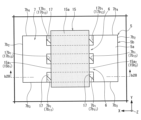
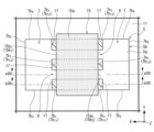
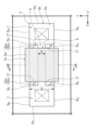
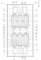
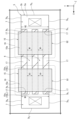
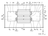
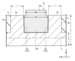
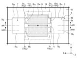
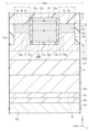
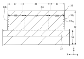
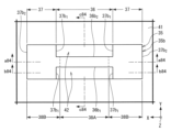
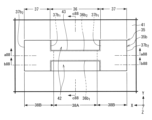
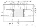
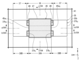
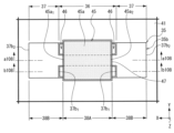
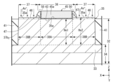
- FIG. 1 is a schematic plan view of essential parts of a configuration example of a semiconductor device according to a first embodiment of the present technology.
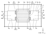
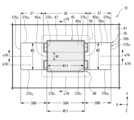
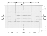
- FIG. 2 is a plan view showing a planar pattern of the semiconductor section in FIG. 1;
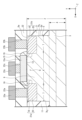
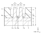
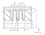
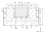
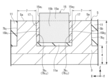
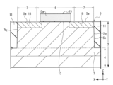
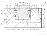
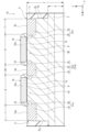
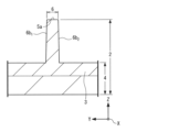
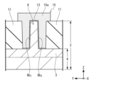
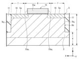
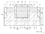
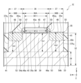
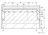
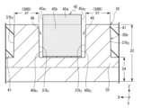
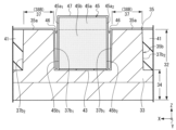
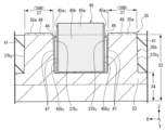
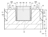
- FIG. 2 is a schematic vertical cross-sectional view showing a vertical cross-sectional structure taken along the a1-a1 cutting line in FIG. 1.
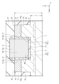
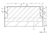
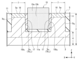
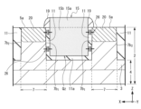
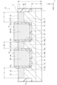
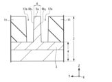
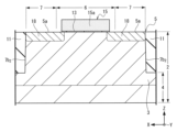
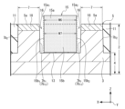
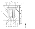
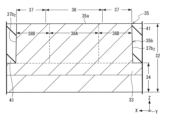
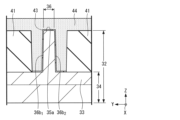
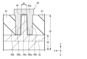
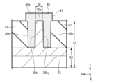
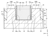
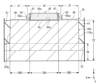
- FIG. 2 is a schematic vertical cross-sectional view showing a vertical cross-sectional structure taken along the b1-b1 cutting line in FIG. 1.
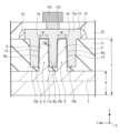
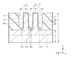
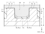
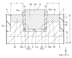
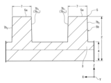
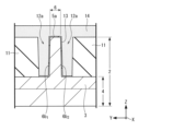
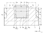
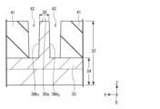
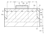
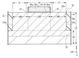
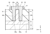
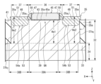
- FIG. FIG. 2 is a schematic vertical cross-sectional view showing a vertical cross-sectional structure taken along the c1-c1 cutting line in FIG. 1.
- FIG. 1 is a schematic plan view of a main part showing steps of a method for manufacturing a semiconductor device according to a first embodiment of the present technology.
- FIG. 6 is a schematic vertical cross-sectional view showing a vertical cross-sectional structure taken along the a5-a5 section line in FIG. 5.
- FIG. 6 is a schematic vertical cross-sectional view showing a vertical cross-sectional structure taken along the b5-b5 cutting line in FIG. 5.
- FIG. 6 is a schematic vertical cross-sectional view showing a vertical cross-sectional structure taken along the c5-c5 cutting line in FIG. 5.
- FIG. FIG. 6 is a schematic plan view of main parts showing a step subsequent to FIG. 5; FIG.
- FIG. 10 is a schematic vertical cross-sectional view showing a vertical cross-sectional structure taken along the line a9-a9 in FIG. 9; 10 is a schematic vertical cross-sectional view showing a vertical cross-sectional structure taken along the b9-b9 cutting line in FIG. 9.
- FIG. 10 is a schematic vertical cross-sectional view showing a vertical cross-sectional structure taken along the c9-c9 cutting line in FIG. 9;
- FIG. 10 is a schematic plan view of main parts showing a step subsequent to FIG. 9;
- 14 is a schematic vertical cross-sectional view showing a vertical cross-sectional structure taken along the b13-b13 cutting line in FIG. 13.
- FIG. 13 is a schematic vertical cross-sectional view showing a vertical cross-sectional structure taken along the line a9-a9 in FIG. 9.
- FIG. 14 is a schematic vertical cross-sectional view showing a vertical cross-sectional structure taken along the c13-c13 cutting line in FIG. 13.
- FIG. FIG. 14 is a schematic plan view of main parts showing a step subsequent to FIG. 13;
- FIG. 17 is a schematic vertical cross-sectional view showing the vertical cross-sectional structure along the a16-a16 cutting line in FIG. 16.
- FIG. 17 is a schematic vertical cross-sectional view showing a vertical cross-sectional structure taken along the b16-b16 cutting line in FIG. 16.
- FIG. 17 is a schematic vertical cross-sectional view showing a vertical cross-sectional structure taken along the c16-c16 cutting line in FIG. 16.
- FIG. 17 is a schematic plan view of main parts showing a step subsequent to FIG. 16;
- FIG. 17 is a schematic plan view of main parts showing a step subsequent to FIG. 16;
- FIG. 21 is a schematic vertical cross-sectional view showing the vertical cross-sectional structure along the a20-a20 cutting line in FIG. 20.
- 21 is a schematic vertical cross-sectional view showing a vertical cross-sectional structure taken along the b20-b20 cutting line in FIG. 20.
- FIG. 21 is a schematic vertical cross-sectional view showing a vertical cross-sectional structure taken along the c20-c20 cutting line in FIG. 20.
- FIG. FIG. 21 is a schematic plan view of main parts showing a step subsequent to FIG. 20;
- FIG. 25 is a schematic vertical cross-sectional view showing the vertical cross-sectional structure along the a24-a24 cutting line in FIG. 24.
- FIG. 25 is a schematic vertical cross-sectional view showing the vertical cross-sectional structure along the b24-b24 cutting line in FIG. 24.
- FIG. 25 is a schematic vertical cross-sectional view showing a vertical cross-sectional structure taken along the c24-c24 cutting line in FIG. 24.
- FIG. 25 is a schematic plan view of main parts showing a step subsequent to FIG. 24;
- FIG. 29 is a schematic vertical cross-sectional view showing a vertical cross-sectional structure taken along the b28-b28 cutting line in FIG. 28.
- FIG. 29 is a schematic plan view of essential parts showing a step subsequent to FIG. 28;
- 31 is a schematic vertical cross-sectional view showing the vertical cross-sectional structure along the a30-a30 cutting line in FIG. 30.
- FIG. 31 is a schematic vertical cross-sectional view showing a vertical cross-sectional structure taken along the b30-b30 cutting line in FIG. 30.
- FIG. FIG. 31 is a schematic plan view of main parts showing a step subsequent to FIG. 30;
- 34 is a schematic vertical cross-sectional view showing a vertical cross-sectional structure taken along the a33-a33 cutting line in FIG. 33.
- FIG. 34 is a schematic vertical cross-sectional view showing a vertical cross-sectional structure taken along the b33-b33 cutting line in FIG. 33.
- FIG. FIG. 3 is a schematic vertical cross-sectional view showing parasitic capacitance added to the field effect transistor of the first embodiment.
- FIG. 3 is a schematic vertical cross-sectional view showing parasitic capacitance added to a field effect transistor of a comparative example.
- FIG. 3 is a schematic vertical cross-sectional view of a semiconductor device according to a modification of the first embodiment of the present technology.
- FIG. 7 is a schematic plan view of a semiconductor device according to a modification of the first embodiment of the present technology.
- FIG. 2 is a schematic vertical cross-sectional view showing a configuration example of a semiconductor device according to a second embodiment of the present technology.
- FIG. 7 is a schematic plan view of a main part of a configuration example of a semiconductor device according to a third embodiment of the present technology.
- FIG. 42 is a schematic vertical cross-sectional view showing a vertical cross-sectional structure taken along the line a41-a41 in FIG. 41.
- FIG. FIG. 42 is a schematic vertical cross-sectional view showing the vertical cross-sectional structure along the b41-b41 cutting line in FIG. 41.
- FIG. FIG. 7 is a schematic plan view of a semiconductor device according to a modification of the third embodiment of the present technology.
- FIG. 7 is a schematic plan view of a main part showing steps of a method for manufacturing a semiconductor device according to a fourth embodiment of the present technology.
- FIG. 46 is a schematic vertical cross-sectional view showing the vertical cross-sectional structure along the a45-a45 cutting line in FIG. 45.
- FIG. 46 is a schematic vertical cross-sectional view showing a vertical cross-sectional structure taken along the b45-b45 cutting line in FIG. 45.
- FIG. FIG. 46 is a schematic vertical cross-sectional view showing a vertical cross-sectional structure taken along the c45-c45 cutting line in FIG. 45;
- FIG. 46 is a schematic plan view of essential parts showing a step subsequent to FIG. 45;
- 50 is a schematic vertical cross-sectional view showing a vertical cross-sectional structure taken along the b49-b49 cutting line in FIG. 49.
- FIG. 50 is a schematic vertical cross-sectional view showing a vertical cross-sectional structure taken along the c49-c49 cutting line in FIG. 49.
- FIG. 49 is a schematic plan view of main parts showing a step subsequent to FIG. 49; 53 is a schematic vertical cross-sectional view showing a vertical cross-sectional structure taken along the a52-a52 cutting line in FIG. 52.
- FIG. FIG. 53 is a schematic vertical cross-sectional view showing a vertical cross-sectional structure taken along the b52-b52 cutting line in FIG. 52.
- 53 is a schematic vertical cross-sectional view showing a vertical cross-sectional structure taken along the c52-c52 cutting line in FIG. 52.
- FIG. FIG. 53 is a schematic plan view of main parts showing a step subsequent to FIG. 52; FIG.
- FIG. 57 is a schematic vertical cross-sectional view showing a vertical cross-sectional structure taken along the a56-a56 cutting line in FIG. 56;
- FIG. 57 is a schematic vertical cross-sectional view showing the vertical cross-sectional structure along the b56-b56 cutting line in FIG. 56.
- FIG. 57 is a schematic vertical cross-sectional view showing a vertical cross-sectional structure taken along the c56-c56 cutting line in FIG. 56;
- FIG. 57 is a schematic plan view of main parts showing a step subsequent to FIG. 56;
- 61 is a schematic vertical cross-sectional view showing the vertical cross-sectional structure along the a60-a60 cutting line in FIG. 60.
- FIG. 61 is a schematic longitudinal sectional view showing a longitudinal sectional structure taken along the b60-b60 cutting line in FIG. 60.
- FIG. FIG. 61 is a schematic plan view of main parts showing a step subsequent to FIG. 60;
- FIG. 64 is a schematic vertical cross-sectional view showing a vertical cross-sectional structure taken along the line a63-a63 in FIG. 63;
- 65 is a schematic longitudinal sectional view enlarging a part of FIG. 64.
- FIG. FIG. 64 is a schematic vertical cross-sectional view showing the vertical cross-sectional structure along the b63-b63 cutting line in FIG. 63.
- 64 is a schematic plan view of essential parts showing a step subsequent to FIG. 63.
- FIG. 67 is a schematic vertical cross-sectional view showing the vertical cross-sectional structure along the a66-a66 cutting line in FIG. 66; 68 is a schematic longitudinal sectional view enlarging a part of FIG. 67.
- FIG. FIG. 67 is a schematic vertical cross-sectional view showing the vertical cross-sectional structure along the b66-b66 cutting line in FIG. 66.
- FIG. 67 is a schematic plan view of essential parts showing a step subsequent to FIG. 66; 70 is a schematic vertical cross-sectional view showing a vertical cross-sectional structure taken along the cutting line a69-a69 in FIG. 69.
- FIG. 70 is a schematic vertical cross-sectional view showing the vertical cross-sectional structure along the b69-b69 cutting line in FIG. 69.
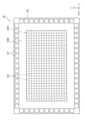
- FIG. FIG. 7 is a schematic plan layout diagram showing a configuration example of a solid-state imaging device according to a fifth embodiment of the present technology.
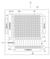
- FIG. 12 is a block diagram illustrating a configuration example of a solid-state imaging device according to a fifth embodiment of the present technology.
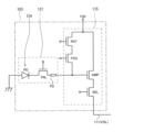
- FIG. 7 is an equivalent circuit diagram showing a configuration example of a pixel and a pixel circuit of a solid-state imaging device according to a fifth embodiment of the present technology.
- FIG. 12 is a schematic vertical cross-sectional view showing a vertical cross-sectional structure of a pixel array section of a solid-state imaging device according to a fifth embodiment of the present technology.
- FIG. 12 is a schematic plan view of essential parts of a configuration example of a semiconductor device according to a sixth embodiment of the present technology.
- FIG. 77 is a schematic vertical cross-sectional view showing a vertical cross-sectional structure taken along the cutting line a76-a76 in FIG. 76;
- FIG. 77 is a schematic vertical cross-sectional view showing a vertical cross-sectional structure taken along the cutting line b76-b76 in FIG.
- FIG. 76; 77 is a schematic vertical cross-sectional view showing a vertical cross-sectional structure taken along the c76-c76 cutting line in FIG. 76.
- FIG. FIG. 7 is a schematic plan view of a main part showing steps of a method for manufacturing a semiconductor device according to a sixth embodiment of the present technology.
- FIG. 81 is a schematic vertical cross-sectional view showing a vertical cross-sectional structure taken along the a80-a80 cutting line in FIG. 80;
- FIG. 81 is a schematic vertical cross-sectional view showing a vertical cross-sectional structure taken along the b80-b80 cutting line in FIG. 80.
- FIG. 81 is a schematic vertical cross-sectional view showing a vertical cross-sectional structure taken along the c80-c80 cutting line in FIG. 80.
- FIG. 81 is a schematic plan view of essential parts showing a step subsequent to FIG. 80;
- 84a is a schematic vertical cross-sectional view showing the vertical cross-sectional structure along the cutting line 84a-a84.
- FIG. 85 is a schematic vertical cross-sectional view showing the vertical cross-sectional structure along the b84-b84 cutting line in FIG. 84.
- FIG. 84c is a schematic vertical cross-sectional view showing the vertical cross-sectional structure along the c84-c84 cutting line in FIG. 84c.
- FIG. FIG. 85 is a schematic plan view of main parts showing a step subsequent to FIG.
- FIG. 89 is a schematic vertical cross-sectional view showing a vertical cross-sectional structure taken along the a88-a88 cutting line in FIG. 88.
- FIG. 89 is a schematic vertical cross-sectional view showing the vertical cross-sectional structure along the b88-b88 cutting line in FIG. 88.
- FIG. 89 is a schematic vertical cross-sectional view showing a vertical cross-sectional structure taken along the c88-c88 cutting line in FIG. 88.
- FIG. 89 is a schematic plan view of essential parts showing a step subsequent to FIG. 88;
- FIG. 93 is a schematic vertical cross-sectional view showing a vertical cross-sectional structure taken along the line a92-a92 in FIG. 92;
- FIG. 93 is a schematic vertical cross-sectional view showing a vertical cross-sectional structure taken along the line a92-a92 in FIG. 92;
- FIG. 93 is a schematic vertical cross-sectional view showing a vertical cross-sectional
- FIG. 93 is a schematic vertical cross-sectional view showing a vertical cross-sectional structure taken along the cutting line b92-b92 in FIG. 92; 93 is a schematic vertical cross-sectional view showing a vertical cross-sectional structure taken along the c928-c92 cutting line in FIG. 92.
- FIG. FIG. 93 is a schematic plan view of main parts showing a step subsequent to FIG. 92;
- FIG. 97 is a schematic vertical cross-sectional view showing a vertical cross-sectional structure taken along the line a96-a96 in FIG. 96;
- FIG. 97 is a schematic vertical cross-sectional view showing a vertical cross-sectional structure taken along the cutting line b96-b96 in FIG. 96.
- FIG. 97 is a schematic vertical cross-sectional view showing a vertical cross-sectional structure taken along the c96-c96 cutting line in FIG. 96;
- FIG. 97 is a schematic plan view of main parts showing a step subsequent to FIG. 96;
- FIG. 100 is a schematic vertical cross-sectional view showing a vertical cross-sectional structure taken along the a100-a100 cutting line in FIG. 100.
- FIG. 100 is a schematic vertical cross-sectional view showing a vertical cross-sectional structure taken along the b100-b100 cutting line in FIG. 100.
- FIG. 100 is a schematic vertical cross-sectional view showing a vertical cross-sectional structure taken along the c100-c100 cutting line in FIG. 100.
- FIG. FIG. 104 is a schematic vertical cross-sectional view showing a vertical cross-sectional structure taken along the b104-b104 cutting line in FIG. 104.
- 105 is a schematic vertical cross-sectional view showing a vertical cross-sectional structure taken along the c104-c104 cutting line in FIG. 104.
- FIG. FIG. 105 is a schematic plan view of main parts showing a step subsequent to FIG. 104; FIG.
- FIG. 108 is a schematic vertical cross-sectional view showing a vertical cross-sectional structure taken along the cutting line a108-a108 in FIG. 108.
- 108 is a schematic vertical cross-sectional view showing the vertical cross-sectional structure along the b108-b108 cutting line in FIG. 108.
- FIG. FIG. 109 is a schematic plan view of main parts showing a step subsequent to FIG. 108;
- 112 is a schematic vertical cross-sectional view showing a vertical cross-sectional structure taken along the cutting line a111-a111 in FIG. 111.
- FIG. FIG. 112 is a schematic vertical cross-sectional view showing a vertical cross-sectional structure taken along the b111-b111 cutting line in FIG. 111.
- FIG. 112 is a schematic vertical cross-sectional view showing a vertical cross-sectional structure taken along the c111-c111 cutting line in FIG. 111.
- FIG. FIG. 111 is a diagram showing a step subsequent to FIG. 111, and is a schematic vertical cross-sectional view showing a vertical cross-sectional structure at the same position as the cutting line a111-a111 in FIG. 111.
- FIG. 115 is a diagram showing a step subsequent to FIG. 115, and is a schematic vertical cross-sectional view showing a vertical cross-sectional structure at the same position as the b111-b111 cutting line in FIG. 111.
- 115 is a diagram showing a step subsequent to FIG.
- FIG. 115 is a diagram showing a step subsequent to FIG. 115, and is a schematic vertical cross-sectional view showing a vertical cross-sectional structure at the same position as the b111-b111 cutting line in FIG. 111.
- FIG. 12 is a schematic vertical cross-sectional view showing a configuration example of a semiconductor device according to a seventh embodiment of the present technology.
- FIG. 7 is a schematic vertical cross-sectional view showing steps of a method for manufacturing a semiconductor device according to a seventh embodiment of the present technology.
- FIG. 120 is a schematic vertical cross-sectional view showing a step subsequent to FIG. 120.
- FIG. 122 is a schematic vertical cross-sectional view showing a step subsequent to FIG. 121.
- FIG. FIG. 12 is a diagram illustrating a configuration example of an electronic device according to an eighth embodiment of the present technology.
- the definitions of directions such as up and down in the following description are simply definitions for convenience of explanation, and do not limit the technical idea of the present technology. For example, if an object is rotated 90 degrees and observed, the top and bottom will be converted to left and right and read, and if the object is rotated 180 degrees and observed, the top and bottom will of course be reversed and read. Further, in the following embodiments, a case where the first conductivity type is p type and the second conductivity type is n type will be exemplified as the conductivity type of the semiconductor, but the conductivity types are selected in the opposite relationship, The first conductivity type may be n-type and the second conductivity type may be p-type.
- a first direction and a second direction that are orthogonal to each other in the same plane are respectively referred to as an X direction and a Y direction
- the first direction and A third direction perpendicular to each of the second directions is defined as a Z direction.
- the thickness direction of the semiconductor layer 2, which will be described later, will be described as the Z direction.
- FIG. 1A the overall configuration of the semiconductor device 1A will be described using FIG. 1, FIG. 1A, and FIGS. 2 to 4.
- the insulating layer 22, contact electrodes 22a, 22b, 22c, and wirings 23a, 23b, 23c shown in FIGS. 2 to 4 are omitted.
- a semiconductor device 1A according to a first embodiment of the present technology includes an island-shaped semiconductor portion 5 provided in a semiconductor layer 2, and this semiconductor portion 5.
- a field effect transistor Q is provided.
- the semiconductor device 1A according to the first embodiment includes an insulating layer 11 provided outside the semiconductor portion 5 so as to surround the semiconductor portion 5.
- the semiconductor layer 2 includes a base portion 4 that extends two-dimensionally in the X direction and the Y direction, and a base portion 4 that protrudes upward (in the Z direction) from the base portion 4.
- An island-shaped semiconductor portion 5 is included.
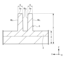
- the semiconductor portion 5 is provided integrally with a first portion 6 extending in the X direction (first direction), and is integrally provided along with the first portion 6 in the X direction (continuing with the first portion 6), and extends in the X direction.
- the semiconductor section 5 of the first embodiment includes, for example, two first portions 6 arranged side by side at a predetermined interval in the Y direction, and an X It has a three-dimensional structure including two second portions 7 provided at both ends in the direction.
- Each of the two first portions 6 and the two second portions 7 has a rectangular planar shape when viewed from above. In the X direction, one end of each of the two first parts 6 is connected to one of the two second parts 7, and the other end of each of the two first parts 6 is It is connected to the other of the two second parts 7 .
- the semiconductor portion 5 is located on the side opposite to the base portion 4 side of the semiconductor portion 5, and has two first portions 6 and two second portions.
- An upper surface portion 5a that extends two-dimensionally across the portion 7; and a side surface portion 5b that extends two-dimensionally in the thickness direction (Z direction) of the semiconductor portion 5 with two first portions 6 and two second portions 7; ,include.
- the side portion 5b includes side portions 6b 1 and 6b 2 located on opposite sides in the Y direction of the first portion 6, and side portions 6b 1 and 6b 2 located on opposite sides in the X direction of the second portion 7. It includes portions 7b 1 and 7b 2 , and side portions 7b 3 and 7b 4 located on opposite sides of the second portion 7 in the Y direction.
- the side surface portions 7b 1 of the second portion 7 are provided at three locations (7b 11 , 7b 12 and 7b 13 ) by a connecting portion where the first portion 6 is connected to the second portion 7 .
- the first side surface portion 7b 1 (7b 11 ) among the three side surface portions 7b 1 is located on the side surface portion 6b 1 side of one of the two first portions 6 .
- the second side surface portion 7b 1 (7b 12 ) among the three side surface portions 7b 1 is located on the side surface portion 6b 1 side of the other first portion 6 of the two first portions 6.
- the remaining third side surface portion 7b 1 (7b 13 ) is located on the side surface portion 6b 2 side of each of the two first portions 6, in other words, between the two first portions 6. .
- the side surface portion 5b of the semiconductor portion 5 includes the side surface portions 6b 1 and 6b 2 of each of the two first portions 6 and the side portions 7b 1 , 7b 2 , 7b 3 and 7b of each of the two second portions 7. 4 and includes.
- the semiconductor portion 5 including the first portion 6 and the second portion 7 can be formed by selectively etching the semiconductor layer 2 to a depth to which the base portion 4 remains.
- the semiconductor layer 2 it is possible to use a semiconductor substrate made of silicon (Si) as the semiconductor material, for example, single crystal as the crystallinity, and p-type as the conductivity type, although the semiconductor layer 2 is not limited thereto.
- the semiconductor layer 2 is provided with a p-type well region 3 made of, for example, a p-type semiconductor region.
- This p-type well region 3 is provided over the entire area of the semiconductor portion 5 and is also provided over the entire area of the surface layer portion of the base portion 4 on the semiconductor portion 5 side.
- the p-type well region 3 is spaced apart from the back surface of the base portion 4 on the side opposite to the semiconductor portion 5 side.
- an insulating layer 11 is provided on the semiconductor portion 5 side of the base portion 4 of the semiconductor layer 2 so as to surround the semiconductor portion 5.
- the insulating layer 11 has a flattened surface layer on the side opposite to the base portion 4 side of the semiconductor layer 2, and has the same height (protrusion amount) as the semiconductor portion 5 except for dug portions 12a and 12b, which will be described later.
- the film thickness is approximately
- the insulating layer 11 is made of, for example, a silicon oxide (SiO 2 ) film.
- an insulating layer is formed so as to cover a head portion 15a of a gate electrode 15 of a field effect transistor Q, which will be described later, and a semiconductor portion 5. 22 are provided.
- This insulating layer 22 is also made of, for example, a silicon oxide (SiO 2 ) film.
- a first wiring layer including wirings 23a, 23b, and 23c is provided on the side of the insulating layer 22 opposite to the semiconductor portion 5 side.
- the wirings 23a, 23b, and 23c of the first wiring layer are made of, for example, a metal film such as aluminum (Al) or copper (Cu), or an alloy film mainly composed of Al or Cu.
- the field effect transistor Q shown in FIG. 1 is configured, for example, of an n-channel conductivity type.
- the field effect transistor Q is constituted by a MOSFET (Metal Oxide Semiconductor Field Effect Transistor) whose gate insulating film is a silicon oxide (SiO 2 ) film.
- the field effect transistor Q may be of p-channel conductivity type.
- a MISFET Metal Insulator Semiconductor FET
- the field effect transistor Q is provided in the semiconductor portion 5 of the semiconductor layer 2. As shown in FIG. The field effect transistor Q is spaced apart from the channel forming part 9 provided in the first part 6 of the semiconductor part 5 and the second part 7 of the semiconductor part 5, and is connected to the channel forming part 9 provided in the first part 6 of the semiconductor part 5 with a gate insulating film 13 interposed therebetween.
- the gate electrode 15 is provided over the upper surface portion 5a and the side surface portions 6b 1 and 6b 2 of the first portion 6.
- the field effect transistor Q also includes a sidewall spacer 19 provided on the sidewall of the gate electrode 15 so as to surround the periphery of the gate electrode 15, and a semiconductor portion 5 on both sides of the gate electrode 15 in the gate length direction (X direction).
- a pair of main electrode regions 21a and 21b are provided and function as a source region and a drain region.
- the gate electrode 15 includes a head portion 15a provided on the upper surface portion 5a side of the first portion 6 of the semiconductor portion 5 with a gate insulating film 13 interposed therebetween; a leg portion 15b that is integrated and provided on the outside of each of two side portions 6b 1 and 6b 2 located on opposite sides of the first portion 6 of the semiconductor portion 5 with a gate insulating film 13 interposed therebetween; has.
- the gate electrode 15 has a structure in which both sides of the first portion 6 of the semiconductor section 5 in the width direction (Y direction) are sandwiched between leg portions 15b. Therefore, the number of leg portions 15b of the gate electrode 15 is usually "n+1" when the number of first portions 6 is "n". In this first embodiment, since two first portions 6 are provided, the gate electrode 15 has three leg portions 15b.
- the head 15a of the gate electrode 15 protrudes above the insulating layer 11.
- Each of the three leg portions 15b of the gate electrode 15 is provided in the insulating layer 11 together with the semiconductor portion 5.
- the gate electrode 15 including the head portion 15a and the leg portions 15b is made of, for example, a polycrystalline silicon (doped polysilicon) film into which impurities are introduced to reduce the resistance value.
- the head 15a has a rectangular shape in plan view, and has a three-dimensional structure having an upper surface and four side surfaces.
- Each of the three leg portions 15b has a three-dimensional structure extending from the head portion 15a in the thickness direction (Z direction) of the semiconductor layer 2 and in the height direction of the semiconductor portion 5, and having a lower surface portion and four side surface portions. It has become.
- the gate electrode 15 has two side surfaces 15a 1 and 15a 2 in the X direction (gate length direction) of the head portion 15a, and two side surfaces 15a 1 and 15a 2 in the X direction (gate length direction) of the leg portion 15b.
- the portions 15b 1 and 5b 2 are flush with each other in cross-sectional view.
- the side surface 15a 1 of the head 15a and the side surface 15b 1 of the leg 15b are constituted by one flat surface extending continuously in the thickness direction (Z direction) of the semiconductor layer 2, and the head
- the side surface 15a 2 of the leg portion 15a and the side surface 15b 2 of the leg portion 15b constitute one flat surface that extends continuously in the thickness direction (Z direction) of the semiconductor layer 2.
- planar view refers to the case viewed from the direction along the thickness direction (Z direction) of the semiconductor layer 2.
- a cross-sectional view refers to a longitudinal section along the thickness direction (Z direction) of the semiconductor layer 2 viewed from a direction (X direction or Y direction) orthogonal to the thickness direction (Z direction) of the semiconductor layer 2. Point.
- the gate insulating film 13 is formed between the first portion 6 of the semiconductor portion 5 and the gate electrode 15, on the top surface portion 5a of the first portion 6 and on the two side surfaces 6b of the first portion 6. 1,6b2 .
- the semiconductor portion 5 since the semiconductor portion 5 has two first portions 6, each of the two first portions 6 extends over the top surface portion 5a and the two side surface portions 6b 1 and 6b 2 . It is provided.
- the gate insulating film 13 is made of, for example, a silicon oxide film.
- the sidewall spacer 19 is provided on the side wall of the head 15a of the gate electrode 15 so as to surround the periphery of the head 15a. That is, the sidewall spacer 19 extends across the first portion 6 on the outside of the gate electrode 15 in the gate length direction (X direction) and the dielectric portion 17, which will be described later, in a plan view. It covers the first portion 6 and the dielectric portion 17 on the outside in the longitudinal direction (X direction).
- the sidewall spacer 19 is provided in alignment with the head portion 15a of the gate electrode 15. In other words, the sidewall spacer 19 is formed in self-alignment with the head 15a of the gate electrode 15.
- the sidewall spacer 19 is formed by, for example, forming an insulating film on the opposite side of the insulating layer 11 from the base portion 4 side so as to cover the gate electrode 15 using a CVD (Chemical Vapor Deposition) method, and then depositing the insulating film on this insulating film. It can be formed by performing anisotropic dry line etching such as RIE (Reactive Ion Etching).
- the sidewall spacer 19 is made of, for example, a silicon oxide film.
- each of the pair of main electrode regions 21a and 21b includes an n-type extension region 18 formed of an n-type semiconductor region provided in the semiconductor section 5 in alignment with the gate electrode 15, and 15, an n-type contact region 20 formed of an n-type semiconductor region provided in the semiconductor portion 5 in alignment with the sidewall spacer 19 on the sidewall 15. That is, each of the pair of main electrode regions 21a and 21b having the n-type extension region 18 and the n-type contact region 20 is provided in the semiconductor portion 5 in alignment with the gate electrode 15.
- the n-type extension region 18 is mainly provided in the first portion 6 of the semiconductor section 5 .
- the n-type contact region 20 is mainly provided in the second portion 7 of the semiconductor section 5 .
- the n-type contact region 20 is provided to spread over the entire second portion 7 of the semiconductor portion 5 in plan view, and is provided on the side surface portions 7b 1 (7b 11 , 7b 12 , 7b 13 ), 7b 2 , 7b 3 and 7b 4 .
- the n-type contact region 20 and the n-type extension region 18 are in contact with each other in the first portion 6 of the semiconductor section 5 .
- each of the n-type extension region 18 and the n-type contact region 20 has a thickness in the thickness direction (Z direction) of the semiconductor layer 2 and in the height direction of the semiconductor section 5.
- the n-type contact region 20 is formed deeper than the n-type extension region 18, in other words, it is formed thicker.
- the field effect transistor Q of the first embodiment has a so-called gate electrode 15 provided on an island-shaped semiconductor portion 5 serving as a fin portion with a gate insulating film 13 interposed therebetween. It is composed of a fin type.
- the length between the pair of main electrode regions 21a and 21b is the channel length L ( ⁇ gate length Lg)
- the length between the gate electrode 15 and the first portion 6 of the semiconductor portion 5 is The length including the width W1 on the top surface 5a side of the first portion 6 and the height of the two side surfaces 6b 1 and 6b 2 of the first portion 6 in the area where The value obtained by multiplying the length) by the number of first portions 6 becomes the channel width W ( ⁇ gate width).
- the channel width W is increased by increasing the width W1 of the first portion 6 of the semiconductor portion 5 and increasing the height of the first portion 6, so that the channel area ( Channel length L ⁇ channel width W) can be increased.
- the channel area (channel length L ⁇ channel width W) can be increased.
- the field effect transistor Q is, for example, an enhancement type (normally off type) in which a drain current flows by applying a gate voltage equal to or higher than a threshold voltage to the gate electrode 15, or a drain current flows even when no voltage is applied to the gate electrode 15. It is composed of a depression type (normally off type) in which the current flows.
- an enhancement type is configured, although the present invention is not limited thereto.
- a channel (inversion layer) electrically connecting the pair of main electrode regions 21a and 21b is formed (induced) in the channel forming portion 9 by the voltage applied to the gate electrode 15.
- a current (drain current) flows from the drain region side (for example, the main electrode region 21b side) through the channel of the channel forming portion 9 to the source region side (for example, the main electrode region 21a side).
- the gate electrode 15 is electrically connected to a wiring 23c on the insulating layer 22 via a contact electrode 22c provided on the insulating layer 22. Further, among the pair of main electrode regions 21a and 21b, one main electrode region 21a is electrically connected to a wiring 23a on the insulating layer 22 via a contact electrode 22a provided on the insulating layer 22. . Of the pair of main electrode regions 21a and 21b, the other main electrode region 21b is electrically connected to the wiring 23b on the insulating layer 22 via a contact electrode 22b provided on the insulating layer 22. .
- a high melting point metal film such as titanium (Ti) or tungsten (W) can be used, for example.
- the semiconductor device 1A according to the first embodiment is provided between the gate electrode 15 and the second portion 7 of the semiconductor section 5 in the X direction (first direction). , and a dielectric portion (separation region) 17 having a lower dielectric constant than the insulating layer 11. Specifically, the dielectric portion 17 is provided between the side surface portion 7 b 1 of the second portion 7 and the leg portion 15 b of the gate electrode 15 .
- the semiconductor portion 5 since the semiconductor portion 5 has two second portions 7, the gap between one of the two second portions 7 and the leg portion 15b of the gate electrode 15 is , and between the other of the two second portions 7 and the leg portion 15b of the gate electrode 15, a dielectric portion 17 is provided, respectively. That is, in this first embodiment, the dielectric portions 17 are provided on both sides of the gate electrode 15 in the gate length direction (X direction).
- the semiconductor section 5 has two first sections 6, the three side surfaces 7b 1 (7b 11 , 7b 12 , 7b 13 ) of the second section 7 and the gate Dielectric portions 17 are provided between the electrodes 15 and the leg portions 15b, respectively.
- the two first portions 6 are separated between the side surface portion 7b 1 of one of the two second portions 7 and the leg portion 15b of the gate electrode 15.
- Three dielectric portions 17 are provided, and two dielectric portions 17 are further provided between the side surface portion 7b1 of the other of the two second portions 7 and the leg portion 15b of the gate electrode 15.
- Three dielectric parts 17 divided into one part 6 are provided.
- the first portion 6 is sandwiched between the side surface portion 7b 1 of the second portion 7 and the leg portion 15b of the gate electrode 15 on both sides of the first portion 6 in the width direction (Y direction). , are each provided with a dielectric portion 17. Then, on the other second portion 7 side, on both sides in the width direction (Y direction) of the first portion 6 between the side surface portion 7b 1 of the other second portion 7 and the leg portion 15b of the gate electrode 15. Dielectric portions 17 are provided so as to sandwich the first portion 6 therebetween.
- the dielectric portion 17 between the side surface portion 7b 11 of the second portion 7 and the leg portion 15b of the gate electrode 15 extends from the upper surface portion 5a side of the second portion 7 to the base portion 4 side (semiconductor It extends in the depth direction (Z direction) of the layer 2 and is connected to the insulating layer 11a provided on the bottom side of the leg portion 15b of the gate electrode 15.
- This dielectric portion 17 electrically isolates the second portion 7 of the semiconductor portion 5 and the leg portion 15b of the gate electrode 15, and also provides a gap between the second portion 7 and the leg portion 15a of the gate electrode 15.
- the first portion 6 and the leg portion 15b of the gate electrode 15 are electrically separated.
- the insulating layer 11a shown in FIG. When forming the trenches (see FIGS. 13 to 15), by forming the trenches 12a and 12b to be shallower than the height (thickness) of the semiconductor section 5, an insulating layer is formed on the bottom surface of each of the trenches 12a and 12b. Part of No. 11 remains.
- the insulating layer 11a is provided, but the insulating layer 11a may not be provided.
- a gate insulating film is interposed between the bottom part of the leg part 15b of the gate electrode 15 and the base part 4 of the semiconductor layer 2.
- the dielectric portion 17 between the side surface portion 7b 11 of the second portion 7 and the leg portion 15b of the gate electrode 15 is illustrated, but the side surface portion 7b 12 of the second portion 7 Also in the dielectric part 17 between the leg part 15b of the gate electrode 15 and the side part 7b 13 of the second part 7 and the leg part 15b of the gate electrode 15, as shown in FIG. It has the same configuration as the dielectric section 17. Therefore, the dielectric portion 17 between the side surface portion 7b 12 of the second portion 7 and the leg portion 15b of the gate electrode 15, and between the side surface portion 7b 13 of the second portion 7 and the leg portion 15b of the gate electrode 15. The dielectric portion 17 will be explained with reference to FIG. 3.
- the dielectric portion 17 between the side surface portion 7b 11 of the second portion 7 and the leg portion 15b of the gate electrode 15 has four sides in plan view that are connected to the first portion 6, It is surrounded by the second portion 7, the leg portion 15b of the gate electrode 15, and the insulating layer 11.
- the dielectric portion 17 between the side surface portion 7b 12 of the second portion 7 and the leg portion 15b of the gate electrode 15 also has four sides in plan view that are connected to the first portion 6, the second portion 7, and the gate. It is surrounded by the leg portion 15b of the electrode 15 and the insulating layer 11.
- the dielectric portion 17 between the side surface portion 7b 13 of the second portion 7 and the leg portion 15b of the gate electrode 15 has two first portions 6, two second portions 7 on all sides in a plan view, It is surrounded by the leg portion 15b of the gate electrode 15.
- the dielectric portion 7 is made of, for example, a dielectric film (low-k film) having a lower dielectric constant than the insulating layer 11, although it is not limited thereto.
- a dielectric film for example, a carbon-added silicon oxide (SiOC) film in which carbon (C) is added to silicon oxide (SiO) can be used.
- This SiOC film has a lower dielectric constant than a silicon oxide film.
- the dielectric constant of a SiOC film is about 1.5 to 2
- the dielectric constant of a silicon oxide film is about 4 to 4.2
- the dielectric constant of air is about 1.
- the dielectric portion 7 preferably has a lower dielectric constant than the gate insulating film 13. Further, the width W3 (see FIG. 3) of the dielectric portion 7 along the X direction is preferably wider than the film thickness W4 (see FIG. 4) of the gate insulating film 11.
- FIGS. 5 to 35 a method for manufacturing the semiconductor device 1A will be described using FIGS. 5 to 35.
- the formation of the field effect transistor Q and the dielectric portion 17 included in the method of manufacturing the semiconductor device 1A will be specifically explained.
- FIG. 5 (schematic main part plan view), FIG. 6 (schematic sectional view taken along the a5-a5 cutting line in FIG. 5), and FIG. 7 (schematic cross-sectional view taken along the b5-b5 cutting line in FIG. 5).
- FIG. 8 (a schematic cross-sectional view taken along the c5-c5 cutting line in FIG. 5)
- an island-shaped semiconductor portion 5 is formed that projects upward from the base portion 4.
- the semiconductor portion 5 includes a first portion 6 extending in the X direction (first direction), and a first portion 6 extending in the Y direction (second direction) that is integrally provided in line with the first portion 6 in the X direction and intersecting the X direction.
- a second portion 7 having a width W1 of the first portion 6 along the width W1 and a second portion 7 having a width W2 in the same direction wider than the width W1 of the first portion 6, and each of the first portion 6 and the second portion 7 has a top surface. It is formed with a three-dimensional structure having a portion 5a and a side portion 5b.
- the side surface portion 5b includes side surface portions 6b 1 and 6b 2 in the first portion 6 and side portions 7b 1 , 7b 2 , 7b 3 and 7b 4 in the second portion 7.
- two first portions 6 placed side by side at a predetermined interval in the Y direction, and both ends of each of the two first portions 6 in the X direction.
- the semiconductor portion 5 is formed to have a three-dimensional structure including two second portions 7 provided in the second portion 7 .
- the side surface portion 5b includes three side surface portions 7b 11 , 7b 12 and 7b 13 divided into three parts by a connecting portion where the first portion 6 is connected to the second portion 7 as the side surface portion 7b 1 .
- the semiconductor portion 5 having the first portion 6 and the second portion 7 can be formed by selectively etching the semiconductor layer 2 to a depth to which the base portion 4 remains.
- the semiconductor layer 2 it is possible to use a semiconductor substrate made of silicon (Si) as the semiconductor material, for example, single crystal as the crystallinity, and p-type as the conductivity type, although the semiconductor layer 2 is not limited thereto. Note that a p-type well region 3 made of a p-type semiconductor region is formed in the semiconductor layer 2 before the semiconductor portion 5 is formed.
- FIG. 9 (schematic main part plan view), FIG. 10 (schematic cross-sectional view along section line a9-a9 in FIG. 9), and FIG. 11 (schematic cross-sectional view along section line b9-b9 in FIG. 9)
- FIG. 12 (schematic cross-sectional view taken along the c9-c9 cutting line in FIG. 9)
- the first portion 6 and the second portion 7 of the semiconductor portion 5 are located outside the semiconductor portion 5 in a plan view.
- An insulating layer 11 surrounding the is formed.
- the insulating layer 11 is formed, for example, by forming a silicon oxide film on the entire surface of the semiconductor layer 2 including the base portion 4 and the semiconductor portion 5 using a well-known film forming method, and then removing the silicon oxide film on the semiconductor portion 5 by CMP. It can be formed by selectively removing it.
- the surface layer portion of the insulating layer 11 on the side opposite to the base portion 4 side is flattened, so that the surface layer portion of the insulating layer 11 and the upper surface portion 5a of the semiconductor portion 5 are substantially flush with each other.
- the insulating layer 11 is formed to have a thickness that is approximately the same as the height (protrusion amount) of the semiconductor portion 5. Further, in this step, an insulating layer 11 flush with the upper surface portion 5a of the semiconductor portion 5 is also formed in a region surrounded by the two first portions 6 and the two second portions 7.
- FIGS. As shown in FIG. 15 (schematic sectional view taken along the c13-c13 cutting line in FIG. 13), the width direction of the first portion 6 of the semiconductor portion 5 ( Recessed portions 12a, 12a and 12b are formed on the outside in the Y direction) to expose the side wall portions 6b 1 and 6b 2 of the first portion 6 and the side wall portions 7b 1 of each of the two second portions 7.
- one dug portion 12a is formed on the side opposite to the other first portion 6 side of one first portion 6 of the two first portions 6,
- the side surface portion 6b 1 of one first portion 6 and the side surface portions 7b 1 (7b 11 ) of each of the two second portions 7 are exposed.
- the other dug portion 12a is formed on the side opposite to the one first portion 6 side of the other first portion 6 of the two first portions 6.
- the side surface portion 6b 1 of the other first portion 6 and the side surface portions 7b 1 (7b 12 ) of each of the two second portions 7 are exposed.
- the dug portion 12b is formed between the two first portions 6, and includes a side surface portion 6b2 of each of the two first portions 6 and a side surface portion 7b1 (7b) of each of the two second portions 7. 13 ) Expose and.
- the dug portions 12a and 12b are formed, for example, to a depth such that a portion of the insulating layer 11 remains as the insulating layer 11a on the bottom surface, although the dug portions 12a and 12b are not limited thereto.
- FIG. 16 (schematic main part plan view), FIG. 17 (schematic sectional view along the a16-a16 cutting line in FIG. 16), and FIG. 18 (schematic cross-sectional view along the b16-b16 cutting line in FIG. 16)
- FIG. 19 (schematic sectional view taken along the c16-c16 cutting line in FIG. 16)
- the upper surface portions 5a of each of the two first portions 6 of the semiconductor section 5 A gate insulating film 13 is formed on each side surface portion 6b 1 , 6b 2 of the portion 6 .
- the gate insulating film 13 can be formed by forming a silicon oxide film on the upper surface portion 5a and side surface portions 6b 1 and 6b 2 of each of the two first portions 6 by, for example, a thermal oxidation method or a deposition method. In this step, the gate insulating film 13 is also formed on the upper surface portion 5a and side surface portions 7b 1 (7b 11 , 7b 12 , 7b 13 ) of the second portion 7 of the semiconductor layer 5.
- FIG. 20 (schematic principal part plan view), FIG. 21 (schematic cross-sectional view along the a20-a20 cutting line in FIG. 20), and FIG. 22 (schematic cross-sectional view along the b20-b20 cutting line in FIG. 20),
- FIG. 23 (schematic cross-sectional view taken along the c20-c20 cutting line in FIG. 20)
- the conductive film 14 for example, a polycrystalline silicon (doped polysilicon) film into which impurities for reducing resistance are introduced during or after film formation can be used.
- the gate insulating film 13 is interposed between the semiconductor portion 5 and the conductive film 14.
- FIG. 24 (schematic main part plan view) and FIG. As shown in FIG. 26 (schematic sectional view taken along section line b24-b24 in FIG. 24), and FIG.
- a gate electrode 15 is formed to be spaced apart from each of the two second portions 7 of the second portion 5 and to face the top surface portion 5a and side portions 6b 1 and 6b 2 of each of the two first portions 6 with the gate insulating film 13 interposed therebetween. do.
- the gate electrode 15 is integrated with a head portion 15 a provided on the upper surface portion 5 a side of the first portion 6 of the semiconductor portion 5 with the gate insulating film 13 interposed therebetween, and is integrated with the head portion 15 and A leg portion 15b is provided on the outside of each of two side surfaces 6b 1 and 6b 2 located on opposite sides of one portion 6 with a gate insulating film 13 interposed therebetween.
- the head 15a includes the recessed portion 12a, the first portion 6, the recessed portion 12b, the first portion 6, and the recessed portion 12a in this order. cross.
- the leg portion 15b is formed in each of the three dug portions 12a, 12b, and 12a, and one end side of each leg portion 15b is connected to the head portion 15a.
- the gate electrode 15 has two side parts 15a 1 and 15a 2 in the X direction (gate length direction) of the head part 15a, and two side parts 15a 1 and 15a 2 in the X direction (gate length direction) of the leg part 15b.
- the two side surfaces 15b 1 and 5b 2 are formed flush with each other in cross-sectional view.
- one side surface portion 15a 1 of the head portion 15a and one side surface portion 15b 1 of the leg portion 15b are constituted by one flat surface extending continuously in the thickness direction (Z direction) of the semiconductor layer 2.
- the other side surface portion 15a 2 of the head portion 15a and the other side surface portion 15b 2 of the leg portion 15b are constituted by one flat surface extending continuously in the thickness direction (Z direction) of the semiconductor layer 2.
- the gate insulating film 13 on the upper surface portion 5a and side surface portion 7b1 of the second portion 7 is removed by side etching and overetching when patterning the conductive film 14.
- an insulating layer is placed in each gap 16.
- a dielectric portion 17 having a relative dielectric constant lower than that of dielectric portion 11 is formed.
- the dielectric part 17 is, for example, a SiOC film having a lower dielectric constant than a silicon oxide film, but is not limited thereto, and is formed on the semiconductor layer 2 including inside the gap part 16, on the semiconductor part 5, and on the insulating layer 11. It can be formed by forming the SiOC film over the entire surface and then selectively removing the SiOC film on the semiconductor portion 5 and the insulating layer 11.
- FIG. 30 (schematic principal part plan view), FIG. 31 (schematic cross-sectional view taken along the a30-a30 cutting line in FIG. 30), and FIG. 32 (schematic cross-sectional view taken along the b30-b30 cutting line in FIG. 30),
- a pair of n-type extension regions 18 made of n-type semiconductor regions are formed in each of the semiconductor parts 5 on both sides of the gate electrode 15 in the X direction.
- the extension region 18 uses the gate electrode 15, the dielectric portion 17, and the insulating layer 11 as a mask for impurity introduction, and exhibits n-type in each semiconductor portion 5 on both sides of the gate electrode 15 in the gate length direction (X direction).
- each of the pair of n-type extension regions 18 is formed in each of the first portion 6 and second portion 7 of the semiconductor portion 5 in alignment with the gate electrode 15. Further, in this step, the dielectric portion 17 functions as a protective layer, and impurity ions are implanted into the semiconductor portion 5 and the base portion 4 through between the second portion 7 of the semiconductor portion 5 and the leg portion 15b of the gate electrode 15. It is possible to suppress the phenomenon caused by
- FIG. 33 (schematic principal part plan view), FIG. 34 (schematic sectional view taken along cutting line a33-a33 in FIG. 33), and FIG. 35 (schematic cross-sectional view taken along cutting line b33-b33 in FIG. 33),
- sidewall spacers 19 are formed on the sidewalls of the head 15a of the gate electrode 15 protruding from the insulating layer 11, including the sidewalls 15a 1 and 15a 2 .
- the sidewall spacer 19 is formed by forming an insulating film on the entire surface of the insulating layer 11 by CVD so as to cover the semiconductor part 5 and the head 15a of the gate electrode 15, and then subjecting this insulating film to a process such as RIE. It can be formed by performing directional dry etching. For example, a silicon oxide film can be used as the insulating film.
- the sidewall spacer 19 is formed on the side wall of the head 15a of the gate electrode 15 so as to surround the head 15a of the gate electrode 15, and is also formed in self-alignment with the gate electrode 15.
- the sidewall spacer 19 extends across the first portion 6 and the dielectric portion 17 on the outside of the gate electrode 15 in the gate length direction, and covers the first portion 6 and the dielectric portion 17 .
- FIG. 33 (schematic principal part plan view), FIG. 34 (schematic sectional view taken along cutting line a33-a33 in FIG. 33), and FIG. 35 (schematic cross-sectional view taken along cutting line b33-b33 in FIG. 33),
- a pair of n-type contact regions 20 made of n-type semiconductor regions are formed in each of the semiconductor portions 5 on both end sides of the gate electrode 15 in the gate length direction (X direction).
- This pair of n-type contact regions 20 is formed by using the insulating layer 11, the gate electrode 15, and the sidewall spacer 19 as a mask for impurity introduction, and forming the semiconductor portion between the insulating layer 11 and the sidewall spacer 19 in a plan view.
- n-type impurities such as arsenic ions (As + ) or phosphorus ions (P + ), and then performing heat treatment to activate the impurities.
- a pair of n-type contact regions 20 are formed across the second portion 7 and the first portion 6 in self-alignment with the sidewall spacer 19 .
- the n-type extension region 18 and the n-type contact region 20 are in contact with each other at the first portion 6 .
- a pair of main electrode regions 21a and 21b including an n-type extension region 18 and an n-type contact region 20 are formed in the semiconductor portion 5.
- the field effect transistor Q shown in FIGS. 1 to 4 is almost completed.
- n-type contact region 20 can be selectively formed in the second portion 6 (only in the second portion 6) by controlling the width of the sidewall spacer 19 in the planar direction.
- FIG. 36 is a schematic vertical cross-sectional view showing the parasitic capacitance added to the field effect transistor Q of this first embodiment.
- FIG. 37 is a schematic vertical cross-sectional view showing the parasitic capacitance added to the field effect transistor Qz of the comparative example.
- an insulating layer 11 surrounding the semiconductor portion 5 is also provided between the second portion 7 of the semiconductor portion 5 and the leg portion 15b of the gate electrode 15.
- the second portion 7 is used as one electrode
- the leg portion 15b of the gate electrode 15 is used as the second electrode
- the insulating layer 11 between the second portion 7 of the semiconductor portion 5 and the leg portion 15b of the gate electrode 15 is A dielectric parasitic amount 26 is added to the field transistor Qz.
- parasitic capacitance 26 deteriorates the noise characteristics of the field effect transistor Qz and becomes a factor that reduces the reliability of the semiconductor device.
- a dielectric portion 17 is provided between the second portion 7 of the semiconductor portion 5 and the leg portion 15b of the gate electrode 15.
- the second portion 7 is used as one electrode
- the leg portion 15a of the gate electrode 15 is used as the second electrode
- the distance between the second portion 7 and the leg portion 15b of the gate electrode 15 is A parasitic amount 25 using the dielectric portion 17 as a dielectric is added to the electric field transistor Q.
- the dielectric portion 17 has a lower dielectric constant than the insulating layer 11. Therefore, the parasitic capacitance 25 added to the field effect transistor Q can be made smaller than the parasitic capacitance 26 added to the field effect transistor Qz of the comparative example.
- the gate electrode 15 having the head portion 15a and the leg portions 15b is formed by processing the conductive film 14 once. Therefore, the two side portions 15a 1 and 15a 2 of the head 15a in the X direction (gate length direction) and the two side portions 15b 1 and 15b 2 of the leg portion 15b in the X direction (gate length direction). They can be made flush with each other in cross-sectional view.
- the head portion 15a and the leg portions 15b of the gate electrode 15 are formed in separate processing steps. Therefore, due to misalignment of the mask and dimensional variations, a step is formed between the head 15a and the leg portions 15b, and this step also varies. Due to this variation in the step difference, the parasitic capacitance Cgd between the gate electrode and the drain region also varies, which deteriorates the noise characteristics of the field effect transistor.
- the side surface portions 15a 1 and 15a 2 of the head portion 15a and the side surface portions 15b 1 and 5b 2 of the leg portion 15b are respectively planar in cross-sectional view. Therefore, the parasitic capacitance Cgd between the gate electrode 15 and the drain region (for example, the main electrode region 21b) is not affected by process variations as in the conventional case. Therefore, according to the method of manufacturing the semiconductor device 1A of the first embodiment, it is possible to suppress deterioration of the noise characteristics of the field effect transistor Q.
- the insulating layer 11 surrounding the semiconductor portion 5 is provided between the second portion 7 of the semiconductor portion 5 and the leg portion 15b of the gate electrode 15. Since the dielectric portion 17 having a low dielectric constant can be formed, deterioration of the noise characteristics of the field effect transistor Q can be further suppressed. This makes it possible to further improve the reliability of the semiconductor device 1A.
- the dielectric portions 17 are provided on both sides of the gate electrode 15 in the gate length direction, but as shown in FIG.
- the dielectric portion 17 may be provided on either side of the direction (direction). That is, the dielectric portion 17 may be provided on at least one of both sides of the gate electrode 15 in the gate length direction.
- the semiconductor section 5 has been described as having two first portions 6 arranged side by side in the Y direction, but the present technology has one first portion 6 as shown in FIG.
- the present invention can also be applied to the semiconductor section 5 having the above structure.
- the dielectric portion 17 may be provided on at least one of both sides of the gate electrode 15 in the gate length direction.
- FIG. 39 shows, as an example, a configuration in which dielectric portions 17 are provided on both sides of the gate electrode 15 in the gate length direction.
- the present technology can also be applied to a semiconductor section 5 having three or more first portions 6 arranged side by side in the Y direction.
- the present technology is also applicable to the case where the field effect transistor Q is configured with a p-channel conductivity type. can do.
- the present technology can also be applied when the field effect transistor Q is configured as a depletion type. .
- a semiconductor device 1B according to the second embodiment of the present technology includes a dielectric section 17B in place of the dielectric section 17 shown in FIG. 3 of the first embodiment described above.
- the dielectric portion 17B includes a cavity portion 17b1 having a lower dielectric constant than the insulating layer 11.
- the cavity portion 17b 1 has low coverage in the gap portion 16 (see FIGS. 24 and 26) between the second portion 7 of the semiconductor portion 5 and the leg portion 15b of the gate electrode 15 in the manufacturing process of the semiconductor device 1B. This can be easily formed by forming the insulating film 17b2 .
- the other configurations are generally similar to the first embodiment described above.
- the film thickness of the insulating film 17b2 from the upper surface part 5a of the semiconductor part 5 to the cavity part 17b1 and the film thickness of the insulating film 17b2 from the cavity part 17b1 to the insulating layer 11a are determined in the step of forming the extension region. In this case, it is preferable to form the layer to such an extent that the impurity to be ion-implanted does not penetrate through it.
- the insulating layer 11a is left as in the first embodiment, but if the insulating layer 11a is not left, it is necessary to control the thickness of the insulating film 17b2 .
- an insulating film having a lower dielectric constant than the insulating layer 11 may be used as the insulating film 17b2 .
- a semiconductor device 1C according to the third embodiment of the present technology basically has the same configuration as the semiconductor device 1A according to the first embodiment described above, except for the following configurations.
- a semiconductor device 1C according to the third embodiment of the present technology includes an island-shaped semiconductor portion 5 provided in a semiconductor layer 2, and a second semiconductor portion provided in this semiconductor portion 5. field effect transistors Q1 and Q2. Further, the semiconductor device 1C according to the third embodiment includes an insulating layer 11 provided outside the semiconductor section 5 so as to surround the semiconductor section 5, similarly to the first embodiment described above.
- the semiconductor layer 2 includes a base portion 4 that extends two-dimensionally in the X direction and the Y direction, and an island-shaped semiconductor portion 5 that projects upward (in the Z direction) from the base portion 4.
- the semiconductor portion 5 of the third embodiment includes two first portions 6 that are arranged side by side at a predetermined distance in the Y direction, and two first portions 6 that are provided at both ends of each of the two first portions 6 in the X direction. It has two second parts 7 and a third part 28 provided in the middle part of the two first parts 6 in the X direction, and the first part 6, the second part 7 and the third part 28 are on the upper surface. It has a three-dimensional structure having a portion 5a and a side portion 5b.
- the semiconductor section 5 of this third embodiment has basically the same configuration as the semiconductor section 5 of the first embodiment described above, except that it includes a third portion 28.
- the third portion 28 has basically the same configuration as the second portion 7. Similarly to the second portion 7, the third portion 28 has a width W5 in the same direction as the width W1 of the first portion 6, which is wider than the width W1 of the first portion 6.
- the third portion 28 has side parts 28b 1 and 28b 2 located on opposite sides in the X direction, and side parts 28b 3 and 28b 4 located on opposite sides in the Y direction. Each of the side surfaces 28b 1 and 28b 2 is divided into three locations by a connecting portion in which the first portion 6 is connected to the third portion 28, and three portions are provided.
- the side surface portion 5b of the semiconductor portion 5 of the third embodiment includes the side surface portions 6b 1 and 6b 2 of each of the two first portions 6 and the side portions 7b 1 and 7b of each of the two second portions 7. 2 , 7b 3 and 7b 4 and side portions 28b 1 , 28b 2 , 28b 3 and 28b 4 of the third portion 28.
- the field effect transistor Q1 is provided in the first portion 6 between one of the two second portions 7 and the third portion 28.
- the field effect transistor Q2 is provided in the first portion 6 between the other of the two second portions 7 and the third portion 28.
- Each of the field effect transistors Q1 and Q2 has the same configuration as the field effect transistor Q of the first embodiment described above.
- a dielectric portion 17 having a lower dielectric constant than the insulating layer 11 surrounding the semiconductor portion 5 is provided. Further, in the semiconductor device 1C of the third embodiment, between the other of the two second portions 7 of the semiconductor section 5 and the leg portion 15b of the gate electrode 15 of the field effect transistor Q2, Similar to the first embodiment described above, a dielectric portion 17 having a lower dielectric constant than the insulating layer 11 surrounding the semiconductor portion 5 is provided.
- the semiconductor device 1C of the third embodiment has an electric field between the third portion 28 of the semiconductor portion 5 and the leg portion 15b of the gate electrode 15 of the field effect transistor Q1, and between the third portion 28 of the semiconductor portion 5 and A dielectric portion 17 having a relative dielectric constant lower than that of the insulating layer 11 surrounding the semiconductor portion 5 is also provided between the leg portion 15b of the gate electrode 15 of the effect transistor Q2.
- field effect transistors Q1 and Q2 are composed of the other main electrode region 21b of the pair of main electrode regions 21a and 21b of field effect transistor Q1, and the pair of main electrode regions 21b of field effect transistor Q2.
- One of the main electrode regions 21a and 21b is shared.
- FIGS. 45 to 69 A method for manufacturing a semiconductor device according to a fourth embodiment of the present technology will be described with reference to FIGS. 45 to 69.
- the formation of the field effect transistor Q and the dielectric portion 17 included in the method of manufacturing a semiconductor device will be specifically explained. Further, in this fourth embodiment, a case will be described in which the gate electrode 15 is formed by processing the conductive film 14 twice.
- FIG. 45 (schematic main part plan view), FIG. 46 (schematic sectional view taken along cutting line a45-a45 in FIG. 45), and FIG. 47 (schematic cross-sectional view taken along cutting line b45-b45 in FIG. 45).
- 48 (a schematic cross-sectional view taken along the line c45-c45 in FIG. 45), an island-shaped semiconductor portion 5 is formed that projects upward from the base portion 4.
- the semiconductor portion 5 includes a first portion 6 extending in the X direction (first direction), and a first portion 6 extending in the Y direction (second direction) that is integrally provided in line with the first portion 6 in the X direction and intersecting the X direction.
- a second portion 7 having a width W1 of the first portion 6 along the width W1 and a second portion 7 having a width W2 in the same direction wider than the width W1 of the first portion 6, and each of the first portion 6 and the second portion 7 has a top surface. It is formed with a three-dimensional structure having a portion 5a and a side portion 5b.
- the side surface portion 5b includes side surface portions 6b 1 and 6b 2 in the first portion 6 and side portions 7b 1 , 7b 2 , 7b 3 and 7b 4 in the second portion 7.
- the semiconductor section 5 is formed with a three-dimensional structure having one first portion 6 and two second portions 7 provided on both ends of the one first portion 6 in the X direction. .
- the semiconductor portion 5 including the first portion 6 and the second portion 7 can be formed by selectively etching the semiconductor layer 2 to a depth such that the base portion 4 remains.
- the semiconductor layer 2 it is possible to use a semiconductor substrate made of silicon (Si) as the semiconductor material, for example, single crystal as the crystallinity, and p-type as the conductivity type, although the semiconductor layer 2 is not limited thereto. Note that a p-type well region 3 made of a p-type semiconductor region is formed in the semiconductor layer 2 before the semiconductor portion 5 is formed.
- an insulating layer 11 surrounding the semiconductor portion 5 is formed in the same manner as in the first embodiment described above.
- the insulating layer 11 on the outside in the width direction (Y direction) of the second portion 6 of the semiconductor section 5 is selectively removed.
- FIG. 50 (schematic sectional view taken along the b49-b49 cutting line in FIG. 49)
- FIG. 51 (schematic sectional view taken along the c49-c49 cutting line in FIG. 49)
- dug portions 12a, 12a are formed to expose the side wall portions 6b 1 , 6b 2 of the first portion 6 and the side wall portion 7b 1 of the second portion 7 .
- one dug portion 12a is formed on the side surface portion 6b1 side of the first portion 6, and is connected to the side surface portion 6b1 of the first portion 6 and the two second portions 7.
- the side surface portions 7b 1 (7b 11 ) of each are exposed.
- the other dug portion 12a is formed on the side surface portion 6b2 of the first portion 6, and the side surface portion 6b2 of the first portion 6 and the two second Each side surface portion 7b 1 (7b 12 ) of the portion 7 is exposed.
- the dug portions 12a and 12a are formed, for example, to a depth that reaches the base portion 4 of the semiconductor layer 2, unlike the first embodiment described above, although the dug portions 12a and 12a are not limited thereto.
- a gate insulating film 13 is formed on the upper surface portion 5a and side surface portions 6b 1 and 6b 2 of the first portion 6 of the semiconductor portion 5.
- the gate insulating film 13 can be formed by forming a silicon oxide film on the top surface 5a and side surfaces 6b 1 and 6b 2 of the first portion 6 by, for example, a thermal oxidation method or a deposition method.
- the gate insulating film 13 is also formed on the upper surface portion 5a and side surface portions 7b 1 (7b 11 , 7b 12 ) of the second portion 7 of the semiconductor layer 5, and on the surface portion of the base portion 4 of the semiconductor layer 2. .
- FIG. 52 (schematic main part plan view), FIG. As shown in FIG. 55 (schematic sectional view taken along cutting line -b52) and FIG. 55 (schematic sectional view taken along cutting line c52-c52 in FIG.
- a conductive film 14 (gate electrode material) covering the semiconductor layer 2 and the insulating layer 11 is formed.
- the conductive film 14 for example, a polycrystalline silicon (doped polysilicon) film into which impurities for reducing resistance are introduced during or after film formation can be used.
- the gate insulating film 13 is interposed between the semiconductor portion 5 and the conductive film 14.
- FIGS. 56 (schematic main part plan view) and FIG. As shown in FIG. 58 (schematic sectional view taken along the b56-b56 cutting line in FIG. 56), and FIG.
- a gate electrode 15 is formed having a width W7 along the X direction and a head 15 whose width W6 in the same direction is also narrower than the width W7 of the leg portions 15b.
- the head portion 15a of the gate electrode 15 is provided on the upper surface side of the first portion 6 of the semiconductor portion 5 with the gate insulating film 13 interposed therebetween, and crosses the first portion 6 in the Y direction.
- the leg portions 15b of the gate electrode 15 are formed in each of the two dug portions 12a, and one end of each leg portion 15b is connected to the head portion 15a.
- one leg portion 15b is provided outside the side surface portion 6b1 of the first portion 6 of the semiconductor portion 5 with the gate insulating film 13 interposed therebetween.
- the other leg portion 15b is provided outside the side surface portion 6b2 of the first portion 6 of the semiconductor portion 5 with the gate insulating film 13 interposed therebetween.
- the gate insulating film 13 on the upper surface portion 5a of the semiconductor portion 5 outside the head portion 15a in the X direction is removed by side etching and overetching when patterning the conductive film 14.
- the conductive film 14 is processed so that the outer leg portions 15b of the head portion 15a are substantially flush with the upper surface portion 5a of the semiconductor portion 5.
- FIG. 60 (schematic principal part plan view), FIG. 61 (schematic sectional view taken along the a60-a60 cutting line in FIG. 60), and FIG. 62 (schematic cross-sectional view taken along the b60-b60 cutting line in FIG. 60),
- a pair of n-type extension regions 18 made of n-type semiconductor regions are formed in each of the semiconductor parts 5 on both sides of the gate electrode 15 in the gate length direction (X direction).
- the extension region 18 is formed by using the head 15a of the gate electrode 15, the outer legs 5b of the head 15a, and the insulating layer 11 as a mask for impurity introduction, and forming the extension region 18 on both sides of the gate electrode 15 in the gate length direction (X direction).
- each of the pair of n-type extension regions 18 is formed in each of the first portion 6 and second portion 7 of the semiconductor portion 5 in alignment with the head portion 15a of the gate electrode 15.
- the leg portions 15b on the outside of the head portion 15a function as a protective layer (impurity introduction suppressing layer), and pass between the second portion 7 of the semiconductor portion 5 and the leg portion 15b of the gate electrode 15. 5 and the base portion 4 can be suppressed from being implanted with impurity ions.
- FIG. 63 (schematic principal part plan view), FIG. 64 (schematic cross-sectional view along section line a63-a63 in FIG. 63), and FIG. 65 (schematic cross-sectional view along section line a63-a63 in FIG. 63),
- the outer legs 15b of the head 15a are selectively removed.
- the outer leg portions 15b of the head 15a are removed using well-known photolithography and dry etching techniques.
- the removal of the outer leg portions 15b of the head portion 15a involves removing the head portion 15a and the leg portions 15b from the semiconductor portion 5 such that the side portions 15a1 and 15a2 on both sides of the head portion 15a in the X direction retreat inward.
- a gap 16 is formed between the side wall portions 7b 1 (7b 11 , 7b 12 ) of the second portion 7 of the semiconductor section 5 and the leg portions 15b of the gate electrode 15.
- two side surfaces 15a 1 , 15a 2 of the head 15a in the X direction (gate length direction) and two side surfaces 15b 1 , 5b 2 of the leg 15b in the X direction (gate length direction) are added . and are formed flush in cross-sectional view.
- one side surface portion 15a 1 of the head portion 15a and one side surface portion 15b 1 of the leg portion 15b are constituted by one flat surface extending continuously in the thickness direction (Z direction) of the semiconductor layer 2.
- the other side surface portion 15a 2 of the head portion 15a and the other side surface portion 15b 2 of the leg portion 15b are constituted by one flat surface extending continuously in the thickness direction (Z direction) of the semiconductor layer 2.
- the width W6 of the head 15a in the X direction and the width W7 of the leg 16b in the X direction are the same design value.
- FIG. 66 (schematic principal part plan view), FIG. 67 (schematic sectional view taken along the b66-b66 cutting line in FIG. 66), and FIG. 68 (schematic cross-sectional view taken along the b66-b66 cutting line in FIG. 66),
- a sidewall spacer 19 is formed on the sidewall of the gate electrode 15 to cover the sidewalls 15a 1 , 15a 2 of the head 15a and the sidewalls 15b 1 , 15b 2 of the leg 15b.
- the sidewall spacer 19 is formed by forming an insulating film on the entire surface of the insulating layer 11 by CVD to fill the gap 16 shown in FIG. 65 and covering the semiconductor part 5 and the head 15a of the gate electrode 15.
- the insulating film can be formed by performing anisotropic dry etching such as RIE.
- a silicon oxide film can be used as the insulating film.
- the sidewall spacer 19 is formed on the side wall of the head 15a of the gate electrode 15 so as to surround the head 15a of the gate electrode 15, and is also formed in self-alignment with the gate electrode 15.
- the sidewall spacer 19 crosses the outer first portion 6 of the gate electrode 15 in the gate length direction in the Y direction.
- the stepped portion 5a1 of the first portion 6 of the semiconductor portion 5 is covered with a sidewall spacer 19. That is, the stepped portion 5a1 is arranged at a position overlapping the sidewall spacer 19 in plan view.
- FIG. 69 (schematic principal part plan view), FIG. 70 (schematic cross-sectional view along section line a69-a69 in FIG. 69), and FIG. 71 (schematic cross-sectional view along section line b69-b69 in FIG. 69),
- a pair of n-type contact regions 20 made of n-type semiconductor regions are formed in each of the semiconductor portions 5 on both end sides of the gate electrode 15 in the gate length direction (X direction).
- This pair of n-type contact regions 20 is formed by using the insulating layer 11, the gate electrode 15, and the sidewall spacer 19 as a mask for impurity introduction, and forming the semiconductor portion between the insulating layer 11 and the sidewall spacer 19 in a plan view.
- n-type impurities such as arsenic ions (As + ) or phosphorus ions (P + ), and then performing heat treatment to activate the impurities.
- a pair of n-type contact regions 20 are formed across the second portion 7 and the first portion 6 in self-alignment with the sidewall spacer 19. In this step, the n-type extension region 18 and the n-type contact region 20 are in contact with each other at the first portion 6 .
- a pair of main electrode regions 21a and 21b including an n-type extension region 18 and an n-type contact region 20 are formed in the semiconductor portion 5.
- the channel forming portion 9 provided in the first portion 5a of the semiconductor portion 5, the upper surface portion 5a and the side portions 6b 1 , 6b 2 of the first portion 6 of the semiconductor portion 5 with the gate insulating film 13 interposed therebetween.
- a gate electrode 15 provided across the gate electrode 15; a sidewall spacer 19 provided on the side wall of the gate electrode 15 across the head portion 15a and the leg portion 15b;
- a field effect transistor Q having a pair of main electrode regions 21a and 21b respectively provided in the semiconductor portion 5 is almost completed.
- n-type contact region 20 of each of the pair of main electrode regions 21a and 21b is selectively formed in the second portion 6 (only in the second portion 6) by controlling the width of the sidewall spacer 19 in the planar direction. can be formed.
- the leg portion 15b remains between the head portion 15a of the gate electrode 15 and the second portion 6 of the semiconductor portion 5 in a state in which the leg portion 15b remains outside the head portion 15a in a plan view.
- An extension region 18 is formed by selectively implanting impurity ions into the semiconductor portion 5 . Therefore, the leg portions 15b on the outside of the head portion 15a function as a protective layer (impurity introduction suppressing layer), and are passed between the second portion 7 of the semiconductor portion 5 and the leg portions 15b of the gate electrode 15 to protect the semiconductor portion 5 and the base. A phenomenon in which impurity ions are implanted into the portion 4 can be suppressed.
- the outer leg portions 15b of the head 15a in plan view are removed by removing the side portions 15a 1 and 15a of the head 15a in the gate length direction (X direction). This is done by etching the head portion 15a and the leg portions 15b all at once in the height direction of the semiconductor portion 5 (thickness direction of the semiconductor layer 2) so that the head portions 15a and leg portions 15b are recessed inward.
- the manufacturing of the first embodiment described above is possible.
- the parasitic capacitance Cgd between the gate electrode 15 and the train region (for example, the main electrode region 21b) is not affected by process variations as in the conventional method. Therefore, also in the method of manufacturing a semiconductor device of the fourth embodiment, it is possible to suppress deterioration of the noise characteristics of the field effect transistor Q.
- the side surfaces 15a 1 and 15a 2 on both sides of the head 15a in the A step portion 5a 1 formed on the upper surface portion 5a of the portion 6 is covered with a sidewall spacer 19.
- the sidewall spacer 19 may be formed of an insulating film having a lower dielectric constant than the insulating layer 11, similar to the dielectric portion 17 of the first embodiment described above.
- the parasitic capacitance 25 added to the field effect transistor Q can be reduced, so deterioration of the noise characteristics of the field effect transistor Q can be suppressed, and the reliability of the semiconductor device can be improved. can be improved.
- CMOS Complementary Metal Oxide Semiconductor
- a solid-state imaging device 1D according to the fifth embodiment of the present technology is mainly configured with a semiconductor chip 102 having a rectangular two-dimensional planar shape when viewed from above. That is, the solid-state imaging device 1D is mounted on the semiconductor chip 102, and the semiconductor chip 102 can be regarded as the solid-state imaging device 1D.
- this solid-state imaging device 1D (201) captures image light (incident light 206) from a subject through an optical lens 202, and calculates the amount of incident light 206 formed on an imaging surface. Each pixel is converted into an electrical signal and output as a pixel signal (image signal).
- the semiconductor chip 102 on which the solid-state imaging device 1D is mounted has a rectangular pixel array section 102A provided at the center in a two-dimensional plane including the X direction and the Y direction that are orthogonal to each other.
- a peripheral portion 102B is provided outside the pixel array portion 102A so as to surround the pixel array portion 102A.
- the semiconductor chip 102 is formed in a manufacturing process by cutting a semiconductor wafer including semiconductor layers 2 and 130, which will be described later, into small pieces for each chip formation region. Therefore, the configuration of the solid-state imaging device 102 described below is generally the same even in a wafer state before the semiconductor wafer is cut into pieces. That is, the present technology is applicable to semiconductor chips and semiconductor wafers.
- a plurality of bonding pads 114 are arranged in the peripheral portion 102B.
- Each of the plurality of bonding pads 114 is arranged, for example, along each of the four sides of the semiconductor chip 102 on a two-dimensional plane.
- Each of the plurality of bonding pads 114 functions as an input/output terminal that electrically connects the semiconductor chip 102 and an external device.
- the semiconductor chip 102 includes a logic circuit 113 shown in FIG. As shown in FIG. 73, the logic circuit 113 includes a vertical drive circuit 104, a column signal processing circuit 105, a horizontal drive circuit 106, an output circuit 107, a control circuit 108, and the like.
- the logic circuit 113 is configured of a CMOS (Complementary MOS) circuit having, for example, an n-channel conductivity type MOSFET (Metal Oxide Semiconductor Field Effect Transistor) and a p-channel conductivity type MOSFET as field effect transistors.
- CMOS Complementary MOS
- the vertical drive circuit 104 is configured by, for example, a shift register.
- the vertical drive circuit 104 sequentially selects desired pixel drive lines 110, supplies pulses for driving the pixels 103 to the selected pixel drive lines 110, and drives each pixel 103 row by row. That is, the vertical drive circuit 104 sequentially selectively scans each pixel 103 of the pixel array section 102A in the vertical direction row by row, and generates a signal charge generated by the photoelectric conversion section (photoelectric conversion element) of each pixel 103 according to the amount of light received.
- a pixel signal from the pixel 103 based on the above is supplied to the column signal processing circuit 105 through the vertical signal line 111.
- the column signal processing circuit 105 is arranged, for example, for each column of pixels 103, and performs signal processing such as noise removal on the signals output from one row of pixels 103 for each pixel column.
- the column signal processing circuit 105 performs signal processing such as CDS (Correlated Double Sampling) and AD (Analog Digital) conversion to remove fixed pattern noise specific to pixels.
- the horizontal drive circuit 106 is composed of, for example, a shift register.
- the horizontal drive circuit 106 sequentially outputs horizontal scanning pulses to the column signal processing circuits 105 to select each of the column signal processing circuits 105 in turn, and select pixels that have undergone signal processing from each of the column signal processing circuits 105.
- the signal is output to the horizontal signal line 112.
- the control circuit 108 generates clock signals and control signals that serve as operating standards for the vertical drive circuit 104, column signal processing circuit 105, horizontal drive circuit 106, etc., based on the vertical synchronization signal, horizontal synchronization signal, and master clock signal. generate. Then, the control circuit 108 outputs the generated clock signal and control signal to the vertical drive circuit 104, column signal processing circuit 105, horizontal drive circuit 106, and the like.
- the photoelectric conversion unit 124 shown in FIG. 74 is composed of, for example, a pn junction type photodiode (PD), and generates a signal charge according to the amount of received light.
- the photoelectric conversion unit 124 has a cathode side electrically connected to the source region of the transfer transistor TR, and an anode side electrically connected to a reference potential line (for example, ground).
- the transfer transistor TR shown in FIG. 74 transfers the signal charge photoelectrically converted by the photoelectric conversion unit 124 to the charge holding region FD.
- the source region of the transfer transistor TR is electrically connected to the cathode side of the photoelectric conversion section 124, and the drain region of the transfer transistor TR is electrically connected to the charge retention region FD.
- the gate electrode of the transfer transistor TR is electrically connected to a transfer transistor drive line among the pixel drive lines 110 (see FIG. 76).
- the charge holding region FD shown in FIG. 74 temporarily holds (accumulates) the signal charges transferred from the photoelectric conversion section 124 via the transfer transistor TR.
- the photoelectric conversion region 121 including the photoelectric conversion unit 124, transfer transistor TR, and charge retention region FD is mounted on a semiconductor layer 130 (see FIG. 75) as a second semiconductor layer to be described later.
- the pixel circuit 115 shown in FIG. 74 reads out the signal charge held in the charge holding region FD, converts the read out signal charge into a pixel signal, and outputs the pixel signal. In other words, the pixel circuit 115 converts the signal charge photoelectrically converted by the photoelectric conversion element PD into a pixel signal based on this signal charge, and outputs the pixel signal.
- the pixel circuit 115 includes, for example, an amplification transistor AMP, a selection transistor SEL, a reset transistor RST, and a switching transistor FDG as pixel transistors, although they are not limited thereto.
- Each of these pixel transistors (AMP, SEL, RST, FDG) and the above-mentioned transfer transistor TR are configured with, for example, a MOSFET as a field effect transistor. Moreover, MISFETs may be used as these transistors.
- the selection transistor SEL, the reset transistor RST, and the switching transistor FDG each function as a switching element
- the amplification transistor AMP functions as an amplification element. That is, the pixel circuit 115 includes field effect transistors for different purposes.
- selection transistor SEL and the switching transistor FDG may be omitted as necessary.
- the amplification transistor AMP has a source region electrically connected to the drain region of the selection transistor SEL, and a drain region electrically connected to the power supply line Vdd and the drain region of the reset transistor RST.
- the gate electrode of the amplification transistor AMP is electrically connected to the charge holding region FD and the source region of the switching transistor FDG.
- the reset transistor RST has a source region electrically connected to the drain region of the switching transistor FDG, and a drain region electrically connected to the power supply line Vdd and the drain region of the amplification transistor AMP.
- the gate electrode of the reset transistor RST is electrically connected to a reset transistor drive line of the pixel drive lines 110 (see FIG. 73).
- the switching transistor FDG has a source region electrically connected to the charge holding region FD and the gate electrode of the amplification transistor AMP, and a drain region electrically connected to the power supply line Vdd and the drain region of the amplification transistor AMP.
- the gate electrode of the switching transistor FDG is electrically connected to a switching transistor drive line of the pixel drive lines 110 (see FIG. 73).
- the source region of the amplification transistor AMP is electrically connected to the vertical signal line 111 (VSL). Furthermore, when the switching transistor FDG is omitted, the source region of the reset transistor RST is electrically connected to the gate electrode of the amplification transistor AMP and the charge holding region FD.
- the transfer transistor TR When the transfer transistor TR is turned on, the transfer transistor TR transfers the signal charge generated by the photoelectric conversion unit 124 to the charge holding region FD.
- the reset transistor RST When the reset transistor RST is turned on, the reset transistor RST resets the potential (signal charge) of the charge holding region FD to the potential of the power supply line Vdd.
- the selection transistor SEL controls the output timing of the pixel signal from the pixel circuit 115.
- the switching transistor FDG controls charge retention by the charge retention region FD, and also adjusts the voltage multiplication factor according to the potential amplified by the amplification transistor AMP.
- the selection transistor SEL becomes conductive, and a current corresponding to the potential of the charge holding region FD amplified by the amplification transistor AMP flows to the vertical signal line 111. Further, by setting the reset control signal applied to the gate electrode of the reset transistor RST of the pixel circuit 115 to a high (H) level, the reset transistor RST becomes conductive, and the signal charge accumulated in the charge holding region FD is reset. .
- FIG. 75 is a schematic vertical cross-sectional view showing the vertical cross-sectional structure of the pixel array section of FIG. 72, and the top and bottom of FIG. 72 are reversed to make the drawing easier to see.
- the semiconductor chip 102 includes a semiconductor layer 130 having a first surface S1 and a second surface S2 located on opposite sides in the thickness direction (Z direction), 1, and a semiconductor layer 2 provided on the opposite side of the insulating layer 131 from the semiconductor layer 130 side.
- the semiconductor chip 102 includes, on the second surface S2 side of the semiconductor layer 130, a flattening layer 141, a color filter layer 142, a lens layer 143, etc., which are sequentially laminated from the second surface S2 side.
- the semiconductor layer 130 is made of, for example, single crystal silicon.
- the planarization layer 141 is made of, for example, a silicon oxide film.
- the planarizing layer 141 is formed on the second surface S2 of the semiconductor layer 130 in the pixel array section 102A so that the second surface S2 (light incident surface) of the semiconductor layer 130 becomes a flat surface with no unevenness. It covers the whole thing.
- color filters such as red (R), green (G), and blue (B) are provided for each pixel 103, and color-separates the incident light incident from the light incident surface side of the semiconductor chip 102. .
- the lens layer 143 is provided with a microlens for each pixel 103 that condenses the irradiation light and allows the condensed light to efficiently enter the photoelectric conversion region 121.
- the semiconductor layer 2 of this fifth embodiment has the same structure as the semiconductor layer 2 shown in FIGS. 2 and 3 of the above-described first embodiment, and the semiconductor layer 2 of the semiconductor layer 2 A field effect transistor Q is provided at 5.
- An insulating layer 11 is provided on the base portion 4 of the semiconductor layer 2 so as to surround the semiconductor portion 5.
- the field effect transistor Q of this fifth embodiment has the same configuration as the field effect transistor Q of the first embodiment described above.
- the semiconductor layer 130 is arranged to overlap the semiconductor portion 5 of the semiconductor layer 2. That is, the semiconductor chip 102 has a two-stage structure in which the semiconductor layer 130 and the semiconductor layer 2 are stacked in the thickness direction (Z direction).
- each of the photoelectric conversion section 124, transfer transistor TR, and charge holding region FD shown in FIG. 74 is provided in the semiconductor layer 130 shown in FIG. 75, although not shown in detail.
- each of the pixel transistors (AMP, SEL, RST, FDG) included in the pixel circuit 115 in FIG. 74 is provided in the semiconductor layer 2 shown in FIG. 75, although not shown in detail.
- Each of the pixel transistors (AMP, SEL, RST, FDG) included in the pixel circuit 115 is constituted by a field effect transistor Q shown in FIG.
- an amplification transistor AMP made up of a field effect transistor Q is illustrated as an example.
- each of the pixel transistors (AMP, SEL, RST, FDG) included in the pixel circuit 115 is configured with a field effect transistor Q. Therefore, in the solid-state imaging device 1D according to the fifth embodiment, the same effects as in the semiconductor device 1A according to the above-described first embodiment can be obtained.
- the present technology is particularly useful when applied to the amplification transistor AMP included in the pixel circuit, in other words, when the amplification transistor AMP is configured with a field effect transistor Q.
- the pixel transistors (AMP, SEL, RST, FDG) included in the pixel circuit 115 are provided in a semiconductor layer 2 different from the semiconductor layer 130 in which the photoelectric conversion section 124, the transfer transistor TR, and the charge retention region FD are provided. Therefore, the degree of freedom in arranging the pixel transistors (AMP, SEL, RST, FDG) included in the pixel circuit 115 can be increased, and the photoelectric conversion section 124, transfer transistor TR, and charge holding region FD can be arranged in the same semiconductor layer. Compared to the case where a pixel transistor or a pixel transistor is provided, higher integration and noise resistance can be achieved.
- At least one of the pixel transistors (AMP, SEL, RST, FDG) included in the pixel circuit 115 may be configured with a field effect transistor Q.
- two of the pixel transistors (AMP, SEL, RST, FDG) included in the pixel circuit 115 are connected to two electric fields provided in one semiconductor section 5. It may also be configured with an effect transistor Q.
- the amplification transistor AMP and the selection transistor SEL are configured by two field effect transistors Q provided in one semiconductor section 5
- the reset transistor RST and the switching transistor FDG are configured by two field effect transistors Q provided in one semiconductor section 5.
- at least one of the pixel transistors (AMP, SEL, RST, FDG) included in the pixel circuit 115 may be configured with a field effect transistor Q6 provided in the semiconductor section 35 of the sixth embodiment described below. .
- FIGS. 76 to 79 the overall configuration of the semiconductor device 1E will be described using FIGS. 76 to 79. Note that for convenience of explanation, illustration of the insulating layer 55 shown in FIGS. 77 to 79 is omitted in FIG. 76. Further, in FIGS. 77 to 79, illustrations of contact electrodes provided on the insulating layer 55 and illustrations of wiring layers and insulating layers above the insulating layer 55 are omitted.
- a semiconductor device 1E according to a sixth embodiment of the present technology includes an island-shaped semiconductor portion 35 provided in a semiconductor layer 32, and a field effect transistor provided in this semiconductor portion 35. It is equipped with Q6 and. Further, the semiconductor device 1E according to the sixth embodiment includes an insulating layer 41 provided outside the semiconductor section 35 so as to surround the semiconductor section 35.
- the semiconductor layer 32 includes a base portion 34 that extends two-dimensionally in the X direction and the Y direction, and an island-shaped semiconductor portion 35 that protrudes upward (in the Z direction) from the base portion 34. including.
- the semiconductor portion 35 includes a first portion 36 extending in the X direction (first direction) and integrally (with the first portion 36) in line with the first portion 36 in the X direction. a second portion 37 which is provided in series) and has a width W2 in the same direction as the width W1 of the first portion 36 along the Y direction intersecting the X direction, which is wider than the width W1 of the first portion 36; Moreover, the first portion 36 and the second portion 37 have a three-dimensional structure having an upper surface portion 35a and a side surface portion 5b.
- the semiconductor portions 35 of the sixth embodiment include, but are not limited to, one first portion 36 extending in the X direction, and one each on both ends of the first portion 36 in the X direction. It has a three-dimensional structure including two second portions 37 provided therein. Each of the one first portion 36 and the two second portions 37 has a rectangular planar shape when viewed from above. In the X direction, one end of the first portion 36 is connected to one of the two second portions 37, and the other end of the first portion 36 is connected to one of the two second portions 37. It is connected to the other second portion 37 of the two.
- the semiconductor section 35 is integrally formed with the first region 38A and on both sides of the first region 38A in the X direction (first direction) along with the first region 38A ( a pair of second regions 38B that are provided (continuously with the first region 38A) and have a height (thickness) He2 in the Z direction higher than a height (thickness) He1 in the Z direction of the first region 38A; Furthermore, it has The first region 38A is provided in the first portion 36.
- One second region 38B of the pair of second regions 38B is provided across one second portion 37 of the two second portions 37 and the first portion 36.
- the other second region 38B of the pair of second regions 38B is provided across the other second portion 37 of the two second portions 37 and the first portion 36.
- the first region 38A includes the semiconductor layer 32.
- the second region 38B unlike the first region 38A, includes a semiconductor layer 32 and an n-type growth layer 48 selectively formed on the upper surface of the semiconductor layer 32 by epitaxial growth.
- the growth layer 48 is formed in alignment with an insulating film 47 provided on the side wall of a gate electrode 45, which will be described later.
- an n-type, p-type, or i-type single crystal layer can be formed by inheriting the crystallinity of the semiconductor layer 32 as a base layer.
- the single crystal layer formed by epitaxial growth is covalently bonded to the semiconductor layer 32, normally when the base layer and the growth layer are of the same type and the same conductivity type or i-type, it is difficult to distinguish between the base layer and the growth layer. I can't stand it.
- the semiconductor layer 32 and the growth layer 48 will be explained separately, but the invention is not limited to this.
- the conductivity types of the base layer and the growth layer are different, it may be possible to distinguish between the base layer and the growth layer by a depletion layer.
- the surface layer portion of the semiconductor layer 32 becomes the upper surface portion 35a
- the surface layer portion of the growth layer 48 becomes the upper surface portion 35a. Therefore, in the semiconductor section 35 of the sixth embodiment, a step is formed on the upper surface section 35a between the first region 38A and the second region 38B.
- the semiconductor section 35 is located on the side opposite to the base section 34 side of the semiconductor section 35, and extends two-dimensionally over the first section 36 and the two second sections 37. It includes a wide upper surface portion 35a and a side surface portion 35b that expands two-dimensionally in the thickness direction (Z direction) of the semiconductor portion 35 with a first portion 36 and two second portions 37.
- the side surface portion 35b has side surface portions 36b 1 and 36b 2 located on opposite sides of the first portion 36 in the Y direction, and side portions 36b 1 and 36b 2 located on opposite sides of the second portion 37 in the X direction.
- the second portion 37 includes side portions 37b 1 and 37b 2 located on opposite sides of the second portion 37 in the Y direction, and side portions 37b 3 and 37b 4 located on opposite sides of the second portion 37 in the Y direction.
- the side surface portion 37b1 of the second portion 37 is divided into two parts by a connecting portion where the first portion 36 is connected to the second portion 37. That is, the side surface portion 5b of the semiconductor portion 35 includes the side surface portions 36b 1 and 36b 2 of the first portion 36 and the side portions 37b 1 , 37b 2 , 37b 3 and 37b 4 of the two second portions 37. include.
- the semiconductor portion 35 including the first portion 36 and the second portion 37 can be formed by selectively etching the semiconductor layer 32 to a depth to which the base portion 34 remains.
- the first region 38A and the second region 38B of the semiconductor section 35 can have a height difference by selectively forming a growth layer 48 on the semiconductor layer 32 of the second region 38B by epitaxial growth.
- a semiconductor substrate can be used that is made of, for example, silicon (Si) as the semiconductor material, single crystal as the crystallinity, and p-type as the conductivity type.
- the growth layer 48 is composed of, for example, a single crystal silicon crystal layer into which an n-type impurity is introduced.
- the height He1 of the first region 38A is defined as the amount of protrusion from the base portion 34 to the upper surface portion 35a of the first region 38A.
- the height He2 of the first region 38B is defined as the amount of protrusion from the base portion 34 to the upper surface portion 35a of the second region 38A.
- the semiconductor layer 32 is provided with a p-type well region 33 made of, for example, a p-type semiconductor region.
- This p-type well region 33 is provided over the entire area of the semiconductor portion 35 and is provided over the entire area of the surface layer portion of the base portion 34 on the semiconductor portion 35 side.
- the p-type well region 33 is spaced apart from the back surface of the base portion 34 on the side opposite to the semiconductor portion 35 side.
- an insulating layer 41 is provided on the semiconductor portion 35 side of the semiconductor layer 32 so as to surround the semiconductor portion 35.
- the insulating layer 41 has a flattened surface layer on the side opposite to the base portion 34 of the semiconductor layer 32, and is flattened except for dug portions 42, 42 (see FIGS. 84, 86, and 87), which will be described later.
- the film thickness is approximately the same as the height He1 of the first region 38A of the portion 35.
- the insulating layer 41 is made of, for example, a silicon oxide (SiO 2 ) film.
- an insulating layer is formed on the side of the insulating layer 41 opposite to the base portion 34 so as to cover the head 45a of the gate electrode 45 of a field effect transistor Q6, which will be described later, and the semiconductor portion 35. 55 are provided.
- This insulating layer 55 is also made of, for example, a silicon oxide (SiO 2 ) film.
- the field effect transistor Q6 shown in FIG. 76 is, for example, of an n-channel conductivity type, although it is not limited thereto.
- the field effect transistor Q6 is constituted by a MOSFET using a silicon oxide (SiO 2 ) film as a gate insulating film.
- the field effect transistor Q6 may be of p-channel conductivity type.
- a MISFET whose gate insulating film is a silicon nitride film or a laminated film (composite film) such as a silicon nitride (Si 3 N 4 ) film and a silicon oxide film may be used.
- the field effect transistor Q6 is provided in the semiconductor portion 35 of the semiconductor layer 32.
- the field effect transistor Q6 includes a gate insulating film that extends over the channel forming portion 39 provided in the first portion 36 of the semiconductor portion 35 and the upper surface portion 5a and side portions 36b 1 and 36b 2 of the first region 38A of the semiconductor portion 35. and a gate electrode 45 provided with a gate electrode 43 interposed therebetween.
- the field effect transistor Q6 also includes an insulating film (separation insulating film) 47 and a sidewall spacer 50 provided on the side wall of the gate electrode 45 so as to surround the gate electrode 45, and a pair of second A pair of main electrode regions 54a and 54b are provided in region 38B and function as a source region and a drain region.
- an insulating film (separation insulating film) 47 and a sidewall spacer 50 provided on the side wall of the gate electrode 45 so as to surround the gate electrode 45, and a pair of second A pair of main electrode regions 54a and 54b are provided in region 38B and function as a source region and a drain region.
- one of the main electrode regions 54a and 54b may be referred to as a source region 54a, and the other main electrode region 54b may be referred to as a drain region 54b.
- the gate electrode 45 has a head portion 45a provided on the upper surface portion 35a side of the first portion 36 (first region 38A) of the semiconductor portion 35 with a gate insulating film 43 interposed therebetween.
- a gate insulating film 43 is formed on the outside of each of two side surfaces 36b 1 and 36b 2 that are integrated with the head 45a and are located on opposite sides of the first portion 36 (first region 38A) of the semiconductor section 35. It has two leg portions 45b provided with the two legs interposed therebetween.
- the gate electrode 45 has a structure in which both sides of the first portion 36 of the semiconductor section 35 in the lateral direction (Y direction) are sandwiched between legs 45b. Therefore, the number of leg portions 45b of the gate electrode 45 is usually "n+1", where the number of first portions 36 is "n”. In this sixth embodiment, since one first portion 36 is provided, the gate electrode 45 has two legs 45b.
- the head 45a of the gate electrode 45 protrudes above the insulating layer 41.
- Each of the two leg portions 45b of the gate electrode 45 is provided in the insulating layer 41 together with the semiconductor portion 35.
- the gate electrode 45 including the head portion 45a and the leg portions 45b is made of, for example, a polycrystalline silicon (doped polysilicon) film into which impurities are introduced to reduce the resistance value.
- the head 45a has a rectangular shape in plan view, and has a three-dimensional structure having an upper surface and four side surfaces.
- Each of the two leg parts 45b has a three-dimensional structure extending from the head part 45a in the thickness direction (Z direction) of the semiconductor layer 32 and in the height direction of the semiconductor part 35, and has a lower surface part and four side parts. It has become.
- the gate electrode 45 has two side surfaces 45a 1 and 45a 2 in the X direction (gate length direction) of the head 45a, and two side surfaces 45a 1 and 45a 2 in the X direction (gate length direction) of the leg portion 45b.
- the portions 45b 1 and 45b 2 are flush with each other in cross-sectional view.
- the side surface portion 45a 1 of the head portion 45a and the side surface portion 45b 1 of the leg portion 45b are constituted by one flat surface extending continuously in the thickness direction (Z direction) of the semiconductor layer 32
- the side surface portion 45a 2 of the leg portion 45a and the side surface portion 45b 2 of the leg portion 45b are configured as one flat surface that extends continuously in the thickness direction (Z direction) of the semiconductor layer 32.
- the planar view refers to the case viewed from the direction along the thickness direction (Z direction) of the semiconductor layer 32.
- a cross-sectional view refers to a longitudinal section along the thickness direction (Z direction) of the semiconductor layer 32 viewed from a direction (X direction or Y direction) orthogonal to the thickness direction (Z direction) of the semiconductor layer 32.
- Point. As shown in FIGS. 76 and 77, the first region 38A of the semiconductor section 35 has a width W11 in the same direction as the gate length direction (X direction, first direction) of the gate electrode 45. It is wider than the width W12 in the longitudinal direction.
- the gate insulating film 43 is arranged between the first portion 36 (first region 38A) of the semiconductor portion 35 and the gate electrode 45 on the upper surface portion 35a of the first portion 36 (first region 38A). , and the two side surfaces 36b 1 and 36b 2 of the first portion 36 (first region 38A).
- the semiconductor section 35 since the semiconductor section 35 has one first section 36, the first section 36 is provided over the top surface section 35a and the two side surfaces 36b 1 and 36b 2 . It is being
- the gate insulating film 43 is made of, for example, a silicon oxide film.
- the insulating film 47 is provided on the side wall of the head 45a of the gate electrode 45 so as to surround the periphery of the head 45a.
- This insulating film 47 is provided for the purpose of electrically insulating and separating the growth layer 48 of the second region 38B of the semiconductor section 35 and the gate electrode 45. Therefore, the insulating film 47 is sometimes called an isolation insulating film 47.
- the insulating film 47 is provided in alignment with the head 45a of the gate electrode 45. In other words, the insulating film 47 is formed in self-alignment with the head 45a of the gate electrode 45.
- the insulating film 47 is formed by, for example, forming a thin silicon oxide film by a CVD (Chemical Vapor Deposition) method so as to cover the gate electrode 45 on the opposite side of the insulating layer 41 from the base portion 34 side, and then, This silicon oxide film is subjected to anisotropic dry etching such as RIE (Reactive Ion Etching) to selectively remove the silicon oxide film on the head 45a of the gate electrode 45 and the silicon oxide film outside the head 45a of the gate electrode 45. It can be formed by removing it.
- the insulating film 47 is preferably formed to have a thickness of, for example, about 2 nm to 10 nm.
- an insulating film 47 is also provided on the side surface portion 37b1 of the second portion 37 of the semiconductor portion 35.
- the sidewall spacer 50 is provided on the side wall of the head 45a of the gate electrode 45 so as to surround the head 45a of the gate electrode 45 with an insulating film 47 interposed therebetween. . That is, the insulating film 47 is formed to have a thickness along the upper surface and side surfaces of the gate electrode 45.
- the sidewall spacer 50 is provided in alignment with the gate electrode 45 and the insulating film 47. In other words, the sidewall spacer 50 is formed in self-alignment with the gate electrode 45 and the insulating film 47.
- the sidewall spacer 50 is formed by, for example, forming an insulating film by CVD on the side of the insulating layer 41 opposite to the base portion 34 so as to cover the gate electrode 45 and the insulating film 47, and then applying RIE to this insulating film. It can be formed by performing anisotropic dry-line etching such as.
- the sidewall spacer 50 is made of, for example, a silicon nitride film.
- the sidewall spacer 50 is provided on the semiconductor portion 35 and on the insulating layer 41 so as to cross the semiconductor portion 35. As shown in FIG. The sidewall spacer 50 is provided such that a portion located on the semiconductor portion 35 is adjacent to the head portion 45a of the gate electrode 45, and the side portion 37b1 of the second portion 37 of the semiconductor portion 35 and the gate electrode in a plan view. 45 is provided adjacent to the head 45a and leg 45b of the gate electrode 45. That is, the sidewall spacer 50 of the sixth embodiment has a portion on the semiconductor section 35 shown in FIG. The length along the height direction (Z direction) of the semiconductor section 35 is different between the part located in the semiconductor part 35 (see FIG. 78), and the part shown in FIG. 78 is longer than the part shown in FIG. 77. There is.
- the sidewall spacer 50 is provided on the growth layer 48 on the outside of the insulating film 47 in the second region 38B of the first portion 36 of the semiconductor section 35, and on the insulating film 47 on the sidewall of the gate electrode 45. formed in alignment. That is, in the second region 38B of the first portion 36 of the semiconductor section 35, a sidewall spacer 50 is formed on the outside of the sidewall of the gate electrode 45, aligned with the insulating film 47 and overlapping with the growth layer 48 in plan view. has been done.
- each of the pair of main electrode regions 54a and 54b includes an n-type semiconductor region 53 aligned with the sidewall spacer 50 and formed across the growth layer 48 and the semiconductor layer 32.
- the n-type semiconductor region 53 is spaced apart from the insulating film 47 on the sidewall of the gate electrode 45.
- the n-type semiconductor region 53 remains as a part of the n-type growth layer 48 between the n-type semiconductor region 53 and the insulating film 47 in the second region 38B of the first portion 36 of the semiconductor section 35. It is in contact with the n-type growth layer 48a, and has a higher impurity concentration than the n-type growth layer 48a.
- the n-type growth layer 48a overlaps the sidewall spacer 50 in plan view.
- the n-type growth layer 48a and the n-type semiconductor region 53 are in contact with the p-type well region 33 to form a pn junction.
- the n-type semiconductor region 53 has a thickness in the thickness direction (Z direction) of the semiconductor layer 32 and in the height direction of the semiconductor section 35 .
- the n-type semiconductor region 53 is formed deeper than the n-type growth layer 48a, in other words, it is formed thicker.
- the n-type semiconductor region 53 is formed across the growth layer 48 and the semiconductor layer 32 in the second region 38B of the semiconductor section 35. That is, each of the pair of main electrode regions 54a and 54b has a structure that protrudes above the first region 38A, in other words, a structure that protrudes upward.
- the field effect transistor Q6 of the sixth embodiment has a so-called gate electrode 45 provided on an island-shaped semiconductor portion 35 as a fin portion with a gate insulating film 43 interposed therebetween. It is composed of a fin type.
- the length between the pair of main electrode regions 54a and 54b is the channel length L ( ⁇ gate length Lg)
- the length between the gate electrode 45 and the first portion 36 of the semiconductor portion 35 is In the area where the two sides overlap three-dimensionally, the width W1 in the transverse direction (Y direction) on the upper surface portion 35a side of the first portion 36 and the height of the two side surfaces 6b 1 and 6b 2 of the first portion 36 are defined as
- the channel width W ( ⁇ gate width) is the value obtained by multiplying the length (periphery of the semiconductor portion 35) by the number of first portions 36.
- the channel width W is increased by increasing the width W1 of the first portion 36 of the semiconductor portion 35 and increasing the height of the first portion 36 in the Z direction.
- the effective channel area (channel length L ⁇ channel width W) can be increased.
- the channel area (channel length L ⁇ channel width W) can be increased.
- the fin-type field effect transistor Q6 can expand its effective channel area without expanding its own occupied area (footprint).
- the field effect transistor Q6 is, for example, an enhancement type (normally off type) in which a drain current flows by applying a gate voltage equal to or higher than a threshold voltage to the gate electrode 45, or a field effect transistor Q6 in which a drain current flows even when no voltage is applied to the gate electrode 45. It can be configured as a flowing depression type (normally off type). In the first embodiment, for example, an enhancement type is configured, although the present invention is not limited thereto.
- a channel (inversion layer) electrically connecting the pair of main electrode regions 54a and 54b is formed (induced) in the channel forming portion 39 by the voltage applied to the gate electrode 45.
- a current (drain current) flows from the drain region side (for example, the main electrode region 54b side) through the channel of the channel forming portion 39 to the source region side (for example, the main electrode region 54a side).
- the gate electrode 4 is provided on the wiring layer on the insulating layer 55 via the contact electrode provided on the insulating layer 55. electrically connected to the connected wiring. Further, among the pair of main electrode regions 54a and 54b, one main electrode region 54a is electrically connected to the wiring provided in the wiring layer on the insulating layer 55 via the contact electrode provided in the insulating layer 55. It is connected. Of the pair of main electrode regions 54a and 54b, the other main electrode region 54b is electrically connected to the wiring provided in the wiring layer on the insulating layer 55 via the contact electrode provided in the insulating layer 55. It is connected.
- tungsten which is a high melting point metal
- a metal material such as aluminum (Al) or copper (Cu), or an alloy material mainly composed of Al or Cu can be used.
- FIGS. 80 to 118 a method for manufacturing the semiconductor device 1E according to the sixth embodiment will be explained using FIGS. 80 to 118. Also in this sixth embodiment, the formation of the semiconductor portion 35 and the charge effect transistor Q6 included in the manufacturing method of the semiconductor device 1E will be specifically explained.
- FIG. 80 (schematic main part plan view), FIG. 81 (schematic sectional view taken along the a80-a80 cutting line in FIG. 80), and FIG. 82 (schematic cross-sectional view taken along the b80-b480 cutting line in FIG. 80).
- 82 (a schematic cross-sectional view taken along the c80-c80 cutting line in FIG. 80)
- an island-shaped semiconductor portion 35 is formed that protrudes upward from the base portion 34.
- the semiconductor portion 35 includes a first portion 36 extending in the X direction (first direction), and a first portion 36 extending in the Y direction (second direction) that is integrally provided in line with the first portion 36 in the X direction and intersecting the X direction.
- the semiconductor is a three-dimensional structure having one first portion 36 and two second portions 37, one each provided on both ends of the one first portion 36 in the X direction. 35 is formed.
- the semiconductor section 35 is provided in a first region 38A in which a gate electrode 45 (see FIG. 96) to be described later is formed, and in a continuous manner with the first region 38A on both sides of the first region 38A in the X direction, and It further includes a pair of second regions 38B and 38B in which an n-type growth layer 48, which will be described later, is formed.
- the first region 38A is provided in the first portion 36.
- One second region 38B of the pair of second regions 38B is provided across one second portion 37 of the two second portions 37 and the first portion 36.
- the other second region 38B of the pair of second regions 38B is provided across the other second portion 37 of the two second portions 37 and the first portion 36.
- the semiconductor portion 35 including the first portion 36 and the second portion 37 and including the first region 38A and the second region 38B is formed by selectively etching the semiconductor layer 32 to a depth to which the base portion 34 remains. can do.
- a semiconductor substrate can be used that is made of, for example, silicon (Si) as the semiconductor material, single crystal as the crystallinity, and p-type as the conductivity type.
- damage is generated on the side surface portions 35b (36b 1 , 36b 2 , 37b 1 to 37b 4 ) of the semiconductor portion 35 due to processing of the semiconductor layer 32.
- a p-type well region 33 made of a p-type semiconductor region is formed in the semiconductor layer 32 before the semiconductor portion 35 is formed.
- an insulating layer 41 surrounding the semiconductor portion 35 is formed in the same manner as the insulating layer 11 shown in FIG. 9 of the first embodiment described above.
- the insulating layer 41 on the outside in the lateral direction (Y direction) of the second portion 36 of the semiconductor section 35 is selectively removed.
- FIG. 85 (schematic sectional view taken along the a84-a84 cutting line in FIG. 84)
- FIG. 86 schematic sectional view taken along the b84-b84 cutting line in FIG. 84
- FIG. 85 (schematic sectional view taken along the b84-b84 cutting line in FIG. 84)
- the side surfaces 36b 1 and 36b 2 of the first portion 36 and the second portion 37 are formed on the outside of the first portion 36 of the semiconductor portion 35 in the lateral direction.
- Digging portions 42a, 42a are formed to expose the side surface portion 37b1 .
- one dug portion 42 is formed on the side surface portion 36b 1 side of the first portion 36, and is connected to the side surface portion 36b 1 of the first portion 36 and this side surface portion 36b 1 .
- the side surface portions 37b1 of each of the two consecutive second portions 37 are exposed.
- the other dug portion 42 is formed on the side surface portion 36b 2 side of the first portion 36, and is connected to the side surface portion 36b 2 of the first portion 36 and this side surface portion 36b.
- the side portions 37b1 of each of the two second portions 37 connected to the second portion 37 are exposed.
- the dug portions 42 and 42 are formed to a depth that reaches, for example, the base portion 34 of the semiconductor layer 32, unlike the above-described first embodiment, although the dug portions 42 and 42 are not limited thereto.
- FIG. 88 (schematic main part plan view), FIG. 89 (schematic sectional view taken along cutting line a88-a88 in FIG. 88), and FIG. 90 (schematic cross-sectional view taken along cutting line b88-b88 in FIG. 88)
- FIG. 91 (schematic cross-sectional view taken along cutting line c88-c88 in FIG. 88)
- the gate insulating film 43 can be formed, for example, by forming a silicon oxide film by a thermal oxidation method or a deposition method. In this step, the gate insulating film 43 is also formed on the upper surface portion 35a and side surface portion 37b 1 of the second portion 37 of the semiconductor portion 35, and on the surface portion of the base portion 34 of the semiconductor layer 32.
- FIG. 92 (schematic plan view of main parts), FIG. As shown in FIG. 95 (schematic sectional view taken along cutting line -b92 in FIG. 92) and FIG. 95 (schematic sectional view taken along cutting line c92-c92 in FIG.
- a conductive film 44 (gate electrode material) is formed to cover the semiconductor portion 35 and the insulating layer 41 in a buried manner.
- the conductive film 44 for example, a polycrystalline silicon (doped polysilicon) film into which impurities to reduce the resistance value are introduced during or after film formation can be used.
- the gate insulating film 43 is interposed between the semiconductor portion 35 and the conductive film 44 .
- FIGS. 96 (schematic main part plan view) and FIG.
- semiconductor A gate electrode that is spaced apart from each of the two second portions 37 of the portion 35 and faces the upper surface portion 5a and side portions 36b 1 and 36b 2 of the first portion 36 (first region 38A) with the gate insulating film 43 interposed therebetween.
- the gate electrode 45 is integrated with a head portion 45 a provided on the upper surface portion 35 a side of the first portion 36 of the semiconductor portion 35 with a gate insulating film 43 interposed therebetween, and is integrated with the head portion 45 .
- the leg portion 45b is provided on the outside of each of the two side surfaces 36b 1 and 36b 2 located on opposite sides of the 1 portion 36 with a gate insulating film 43 interposed therebetween.
- the head 45a crosses one of the dug portions 42, the first portion 36, and the other dug portion 42 in this order in the lateral direction (Y direction) of the first portion 36 of the semiconductor portion 35.
- Each of the two leg parts 45b is individually formed in each of the two dug parts 42, and one end side of each is connected to the head 45a.
- the gate electrode 45 has two side parts 45a 1 and 45a 2 in the X direction (gate length direction) of the head 45a, and two side parts 45a 1 and 45a 2 in the X direction (gate length direction) of the leg part 45b.
- the two side surfaces 45b 1 and 45b 2 are formed flush with each other in cross-sectional view.
- one side surface portion 45a 1 of the head portion 45a and one side surface portion 45b 1 of the leg portion 45b are constituted by one flat surface extending continuously in the height direction (Z direction) of the semiconductor portion 35.
- the other side surface portion 45a 2 of the head portion 45a and the other side surface portion 45b 2 of the leg portion 45b are constituted by one flat surface extending continuously in the height direction (Z direction) of the semiconductor portion 35.
- a gap 46 is formed between the side surface 7b1 of the second portion 37 of the semiconductor section 35 and the leg 45b of the gate electrode 45.
- the gap portion 46 on the side surface portion 36b1 side of the first portion 36 is illustrated as an example.
- the semiconductor portion 35 since the semiconductor portion 35 has one first portion 36 and two second portions 37, the gap portion 46 is formed on both sides (two sides) of the gate electrode 45 in the gate length direction in a plan view. two second portions 37).
- the gate insulating film 43 on the upper surface portion 35a and side surface portion 37b1 of the second portion 37 of the semiconductor portion 35 is removed by side etching and overetching when patterning the conductive film 44.
- a gate is added to the first region 38A of the semiconductor portion 35, which faces the upper surface portion 35a and side surface portion 35b of the first region 38A with the gate insulating film 43 interposed therebetween. Electrode 45 is formed.
- FIG. 100 (schematic principal part plan view), FIG. 101 (schematic cross-sectional view along the a100-a100 cutting line in FIG. 100), and FIG. 102 (schematic cross-sectional view along the b100-b100 cutting line in FIG. 100),
- FIG. 103 (schematic cross-sectional view taken along the c100-c100 cutting line in FIG. 100)
- the insulating film 47 can be formed, for example, by depositing a silicon oxide film using a CVD method.
- the insulating film 47 is for electrically insulating and separating the gate electrode 45 and a growth layer 48 (see FIGS.
- the insulating film 47 is formed to have a thickness along the upper surface and side surfaces of the gate electrode 45. In this step, as shown in FIG. 102, the insulating film 47 is formed over the side surfaces 45a 1 and 45a 2 of the head 45a of the gate electrode 45 and the side surfaces 45b 1 and 45b 2 of the leg 45b. . Further, the insulating film 47 is also formed on the side surface portion 37b1 of the second portion 37 of the semiconductor portion 35.
- an insulating film 47 on the gate electrode 45 and outside the gate electrode 45 is selectively removed so that the insulating film 47 remains on the side walls of the gate electrode 45, and as shown in FIG. 105 (schematic sectional view taken along section line a104-a104 in FIG. 104), FIG. 106 (schematic sectional view taken along section line b104-b104 in FIG. 104), and FIG. 107 (schematic sectional view taken along section line c104-c104 in FIG. 104)
- an insulating film 47 is formed on the side walls of the gate electrode 45 to cover the side walls of the gate electrode 45.
- Selective removal of the insulating film 47 can be performed by anisotropic dry etching such as RIE. Further, selective removal of the insulating film 47 can also be performed by patterning the insulating film 47 using an etching mask.
- a growth layer 48 is selectively grown by epitaxial growth on the upper surface portion 35a of each of the pair of second regions 38B and 38B located on both sides in the X direction of the first region 38A in which the gate electrode 45 is formed.
- FIG. 109 schematic sectional view taken along cutting line a108-a108 in FIG. 108
- FIG. 110 schematic diagram taken along cutting line b108-b108 in FIG. 108.
- the height (thickness) He2 in the Z direction of each of the pair of second regions 38B and 38B is set higher than the height (thickness) He1 in the Z direction of the first region 38A ( thick). Since the growth layer 48 is formed by inheriting the crystallinity of the semiconductor layer 32 as the base, it is formed as a crystal layer of single crystal silicon into which an n-type impurity is introduced, for example.
- the growth layer 48 is formed in alignment with the gate electrode 45 and the insulating film 47.
- the growth layer 48 is formed to be insulated and separated from the gate electrode 45 by the insulating film 47.
- the growth layer 48 is basically formed on the side surface portion 37b 1 of the second portion 37.
- the first region 38A of the semiconductor section 35 includes the semiconductor layer 32, and the surface layer portion of the semiconductor layer 32 becomes the upper surface portion 35a.
- the second region 38B of the semiconductor section 35 includes the semiconductor layer 32 and the growth layer 48, and the surface portion of the growth layer 48 becomes the upper surface portion 35a.
- FIG. 111 (schematic main part plan view), FIG. 112 (schematic sectional view along the a111-a111 cutting line in FIG. 111), and FIG. 113 (schematic cross-sectional view along the b111-b111 cutting line in FIG. 111),
- FIG. 114 (schematic cross-sectional view taken along the c111-c111 cutting line in FIG. 111)
- side portions 45a 1 and 45a 2 of the head 45a and the leg portions 45b are formed on the side wall of the gate electrode 45.
- a sidewall spacer 50 is formed to cover the side surfaces 45b 1 and 45b 2 .
- the sidewall spacer 50 is formed by forming an insulating film on the entire surface of the insulating layer 41 by CVD so as to fill the gap 46 shown in FIG. 110 and covering the semiconductor part 35 and the head 45a of the gate electrode 45. Thereafter, the insulating film can be formed by performing anisotropic dry etching such as RIE. For example, a silicon oxide film can be used as the insulating film.
- the sidewall spacer 50 is formed on the sidewall of the head 45a of the gate electrode 45 with an insulating film 47 interposed therebetween, and is self-contained with respect to the gate electrode 45. Formed by alignment.
- the sidewall spacer 50 crosses the first portion 36 of the gate electrode 45 on the outside in the gate length direction in the Y direction. Further, in this step, as shown in FIGS. 112 and 113, the sidewall spacer 50 is formed to overlap with the growth layer 48 of the second region 38B of the semiconductor section 35 in plan view.
- FIGS. As shown in a schematic vertical cross - sectional view taken at the same position as the b111-b111 cutting line in FIG. Inject selectively.
- phosphorus ions P +
- P + phosphorus ions
- FIG. 118 (schematic longitudinal sectional view taken at the same position as the b111-b111 cutting line in FIG. 111), a pair of n-type semiconductor Regions 53 and 53 are formed.
- Each of the pair of n-type semiconductor regions 53 is aligned with the sidewall spacer 50 and is formed across the growth layer 48 and the semiconductor layer 32 .
- Each of the pair of n-type semiconductor regions 53 remains as a part of the n-type growth layer 48 between the n-type semiconductor region 53 and the insulating film 47 in the second region 38B of the semiconductor section 35. It is formed in contact with the n-type growth layer 48a and with a higher impurity concentration than the n-type growth layer 48a.
- the n-type growth layer 48a overlaps the sidewall spacer 50 in plan view.
- a pair of main electrode regions 54a and 54b each including an n-type semiconductor region 53 is formed in the pair of second regions 38B of the semiconductor section 35. Further, in this step, a channel forming portion 39 is formed in the semiconductor portion 35 between the pair of main electrode regions 54a and 54b. Further, in this step, a field effect transistor Q6 having a gate insulating film 43, a gate electrode 45, a pair of main electrode regions 54a and 54b, a channel forming part 39, and the like is formed in the semiconductor part 35. Furthermore, in this step, each of the pair of main electrode regions 54a and 54b is formed to have a structure that protrudes above the first region 38A (a structure that protrudes upward).
- an insulating layer 55 is formed on the insulating layer 41 to cover the semiconductor portion 35 and the field effect transistor Q6, and the surface layer portion of the insulating layer 55 on the side opposite to the semiconductor portion 35 is planarized. Then, the state shown in FIG. 79 is reached.
- the semiconductor device 1E according to the sixth embodiment includes a semiconductor section 35 and a field effect transistor Q6 provided in the semiconductor section 35.
- the semiconductor portion 35 is provided in a continuous manner with the first region 38A on both sides of the first region 38A in the X direction (first direction), and is higher than the height He1 of the first region 38A.
- the field effect transistor Q6 has a gate electrode 45 provided on the upper surface portion 35a and side portions 35b 1 and 35b 2 of the first region 38A with a gate insulating film 43 interposed therebetween, and a gate electrode 45 provided on the upper surface portion 35a and the side portions 35b 1 and 35b 2 of the first region 38A, and a gate electrode 45 provided on the pair of second regions 38B and 38B.
- a pair of main electrode regions 54a and 54b are provided. Therefore, according to the semiconductor device 1E according to the sixth embodiment, the pair of main electrode regions 54a and 54b has a structure in which the pair of main electrode regions 54a and 54b protrudes above the first region 38A of the semiconductor section 35. Compared to the conventional structure in which the second region 38A and the second region 38B are flat, the effective channel length is increased, so that short channel effects can be suppressed. Thereby, the reliability of the semiconductor device 1E can be improved.
- the gate electrode 45 having the head portion 45a and the leg portions 45b is formed by processing the conductive film 44 once. Therefore, the two side portions 45a 1 and 45a 2 of the head 45a in the X direction (gate length direction) and the two side portions 45b 1 and 45b 2 of the leg portion 45b in the X direction (gate length direction). They can be made flush with each other in cross-sectional view.
- the side portions 45a 1 and 45a 2 of the head portion 45a and the side portions 45b 1 and 45b 2 of the leg portion 45b are flush with each other in cross-sectional view. Therefore, similarly to the first embodiment described above, the parasitic capacitance Cgd between the gate electrode 45 and the train region (for example, the main electrode region 54b) is not affected by process variations as in the conventional case. . Therefore, according to the method of manufacturing the semiconductor device 1E of the sixth embodiment, it is possible to suppress deterioration of the noise characteristics of the field effect transistor Q6, as in the first embodiment described above.
- a pair of main electrodes are provided in a pair of second regions 48B and 48B having a height He2 higher than a height He1 of the first region 48A of the semiconductor section 35.
- the pair of main electrode regions 54a and 54b can be structured to protrude above the first region 38A of the semiconductor section 35.
- the effective channel length of the field effect transistor Q6 is increased, and short channel effects can be suppressed. Therefore, according to the method for manufacturing a semiconductor device 1E according to the sixth embodiment, a highly reliable semiconductor device 1E can be manufactured.
- the growth layer 48 is selectively formed by epitaxial growth with the side surface portion 37b 1 of the second portion 37 (second region 38B) of the semiconductor portion 35 covered with the insulating film 47.
- the side surface portion 37b1 of the second portion 37 (second region 38B) of the semiconductor portion 35 does not necessarily need to be covered with an insulating film. That is, when the semiconductor layer 32 is processed to form the semiconductor portion 35, etching damage is generated on the side surface portion 35b of the semiconductor portion 35 due to the processing of the semiconductor layer 32.
- the side surface portion 37b 1 of the second portion 37 (second region 38B) of the semiconductor portion 35 may be damaged by epitaxial growth .
- No crystalline layer is formed. Therefore, the growth layer 48 can be selectively formed on the upper surface of the second region 38B of the semiconductor portion 35 by epitaxial growth without covering the side surface portion 37b1 of the second portion 37 (second region 38B) with an insulating film. can. Furthermore, unlike the polycrystalline growth layer 48, even if polycrystalline or amorphous growth layers are formed on the side surface portion 37b1 of the second portion 37 (second region 38B), these growth layers can be selectively removed. can do.
- the semiconductor device 1F according to the seventh embodiment of the present technology basically has the same configuration as the semiconductor device 1E according to the above-described sixth embodiment, but differs in the configuration of the semiconductor section.
- the semiconductor section 35 of the sixth embodiment described above has a structure in which one growth layer 48 is provided in the second region 38B.
- the semiconductor section 35 of the seventh embodiment has a structure in which two growth layers 48 and 51 are provided in the second region 38B.
- the two growth layers 48 and 51 are achieved by selectively forming the growth layer 51 on the growth layer 48 by epitaxial growth after forming the sidewall spacer 50 in the manufacturing process of the semiconductor device 1F.
- steps similar to those in the sixth embodiment described above are performed to form up to the sidewall spacer 50.
- a growth layer 51 is selectively formed on the upper surface of each growth layer 48 by epitaxial growth. Since the growth layer 51 is formed by inheriting the crystallinity of the growth layer 48 as the base, it can be formed, for example, as a crystal layer of single crystal silicon into which an n-type impurity is introduced.
- the growth layer 51 is formed in alignment with the sidewall spacers 50.
- the growth layer 51 is formed to be insulated and separated from the gate electrode 45 by the sidewall spacer 50 and the insulating film 47.
- each of the pair of second regions 38B and 38B of the semiconductor section 35 has a configuration including the semiconductor layer 32 and the growth layers 48 and 51, and the surface layer portion of the growth layer 51 becomes the upper surface portion 35a. This can be achieved by making the height (thickness) He2 in the Z direction of each of the pair of second regions 38B and 38B higher (thicker) than the height (thickness) He1 in the Z direction of the first region 38A.
- an n-type impurity such as arsenic ion ( As + ) is selectively injected.
- As + arsenic ion
- phosphorus ions P +
- a pair of n-type semiconductor regions 53 and 53 are formed in each of the two regions 38B and 38B.
- Each of the pair of n-type semiconductor regions 53 is aligned with the sidewall spacer 50 and is formed across the growth layer 51, the growth layer 48, and the semiconductor layer 32.
- Each of the pair of n-type semiconductor regions 53 remains as a part of the n-type growth layer 48 between the n-type semiconductor region 53 and the insulating film 47 in the second region 38B of the semiconductor section 35. It is formed in contact with the n-type growth layer 48a and with a higher impurity concentration than the n-type growth layer 48a.
- the n-type growth layer 48a overlaps the sidewall spacer 50 in plan view.
- a pair of main electrode regions 54a and 54b each including an n-type semiconductor region 53 is formed in a pair of second regions 38B and 38B of the semiconductor section 35. Further, in this step, a channel forming portion 39 is formed in the semiconductor portion 35 between the pair of main electrode regions 54a and 54b. Further, in this step, a field effect transistor Q6 having a gate insulating film 43, a gate electrode 45, a pair of main electrode regions 54a and 54b, a channel forming part 39, and the like is formed in the semiconductor part 35. Further, in this step, the pair of main electrode regions 54a and 54b are formed to have a structure that protrudes above the first region 38A of the semiconductor section 35 (a structure that protrudes upward).
- an insulating layer 55 is formed on the insulating layer 41 to cover the semiconductor portion 35 and the field effect transistor Q6, and the surface layer portion of the insulating layer 55 on the side opposite to the semiconductor portion 35 is planarized. The state shown in is reached.
- the present technology can be applied to various electronic devices, such as imaging devices such as digital still cameras and digital video cameras, mobile phones with an imaging function, or other devices with an imaging function. can do.
- FIG. 123 is a diagram showing a schematic configuration of an electronic device (for example, a camera) according to the sixth embodiment of the present technology.
- the electronic device 200 includes a solid-state imaging device 201, an optical lens 202, a shutter device 203, a drive circuit 204, and a signal processing circuit 205.
- This electronic device 200 shows an embodiment in which a solid-state imaging device 1D according to the fifth embodiment of the present technology is used as the solid-state imaging device 201 in an electronic device (for example, a camera).
- the optical lens 202 forms an image of image light (incident light 206) from the subject onto the imaging surface of the solid-state imaging device 201.
- image light incident light 206
- the shutter device 203 controls the light irradiation period and the light blocking period to the solid-state imaging device 201.
- the drive circuit 204 supplies drive signals that control the transfer operation of the solid-state imaging device 201 and the shutter operation of the shutter device 203.
- Signal transfer of the solid-state imaging device 201 is performed by a drive signal (timing signal) supplied from the drive circuit 204.
- the signal processing circuit 205 performs various signal processing on the signal (pixel signal (image signal)) output from the solid-state imaging device 201.
- the video signal on which the signal processing has been performed is stored in a storage medium such as a memory, or is output to.
- the electronic device 200 to which the solid-state imaging device of the above-described embodiment can be applied is not limited to a camera, but can also be applied to other electronic devices.
- the present invention may be applied to an imaging device such as a camera module for mobile devices such as a mobile phone or a tablet terminal.
- this technology can be applied to light detection devices in general, including distance sensors called ToF (Time of Flight) sensors that measure distance.
- a distance measurement sensor emits illumination light toward an object, detects the reflected light that is reflected from the object's surface, and measures the time from when the illumination light is emitted until the reflected light is received. This is a sensor that calculates the distance to an object based on flight time.
- the structure of the element isolation region of this distance measurement sensor the structure of the element isolation region described above can be adopted.
- the present technology can also be applied to a field effect transistor in which a channel forming portion and a gate electrode are provided at the corner portions of a semiconductor portion having an L-shaped planar shape.
- the island-shaped semiconductor portion 5 that is integrated with the base portion 4 of the semiconductor layer 2 has been described as the semiconductor portion.
- the present technology is not limited to the island-shaped semiconductor portion 5 integrated with the base portion 4.
- the present technology can also be applied to a so-called SOI (Silicon On Insulator) structure in which a semiconductor section is provided on an insulating layer.
- SOI Silicon On Insulator
- the semiconductor portion has a bottom portion in contact with the insulating layer on the opposite side from the top portion.
- the present technology can also be applied to a semiconductor device in which a fin-type field effect transistor and a planar-type field effect transistor are mixed.
- the present technology may have the following configuration.
- the first portion is integrally provided along with the first portion in a first direction, and has a width in the same direction as the width of the first portion along a second direction intersecting the first direction. a second portion wider than the width of the second portion, and each of the first portion and the second portion includes the top surface portion and the side surface portion; an insulating layer surrounding each of the first portion and the second portion; a field effect transistor having a gate electrode spaced apart from the second portion and provided across the top surface portion and the side surface portion of the first portion; a dielectric portion provided between the gate electrode and the second portion and having a lower dielectric constant than the insulating layer;
- a semiconductor device equipped with (2) The semiconductor device according to (1) above, wherein the dielectric portion includes a dielectric film having a dielectric constant lower than that of the insulating layer.
- the dielectric portion includes a cavity portion having a dielectric constant lower than that of the insulating layer.
- the field effect transistor further includes a gate insulating film interposed between the first portion and the gate electrode, The semiconductor device according to any one of (1) to (3) above, wherein the dielectric portion has a lower dielectric constant than the gate insulating film.
- the width of the dielectric portion along the first direction is wider than the thickness of the gate insulating film.
- the gate electrode has a head that protrudes above the insulating layer, and a leg that is integrated with the head and provided in the insulating layer, The semiconductor according to any one of (1) to (5) above, wherein a side surface of the head in the first direction and a side surface of the leg in the first direction are flush with each other in cross-sectional view.
- the gate electrode has a head that projects upward from the insulating layer, and a leg that is integrated with the head and provided in the insulating layer, The semiconductor device according to any one of (1) to (6) above, wherein the dielectric portion is surrounded on all sides by the first portion, the second portion, the leg portion, and the insulating layer in a plan view. .
- the field effect transistor further includes a pair of main electrode regions provided in the semiconductor portion on both sides of the gate electrode in the gate length direction. .
- the field effect transistor further includes a sidewall spacer provided on a sidewall of the gate electrode, Each of the pair of main electrode regions includes an extension region provided in the semiconductor portion in alignment with the gate electrode, and an extension region provided in the semiconductor portion in alignment with the sidewall spacer, and with a lower impurity content than the extension region.
- the semiconductor device further comprising a photoelectric conversion section and a pixel circuit that converts signal charges photoelectrically converted by the photoelectric conversion section into pixel signals,
- the semiconductor device according to any one of (1) to (9) above, wherein at least one of a plurality of pixel transistors included in the pixel circuit is configured with the field effect transistor.
- the semiconductor device according to (10) above, further comprising a semiconductor layer arranged to overlap with the semiconductor section in plan view and provided with the photoelectric conversion section.
- the first portion is integrally provided along with the first portion in a first direction, and has a width in the same direction as the width of the first portion along a second direction intersecting the first direction.
- a method for manufacturing a semiconductor device including. (13) The method for manufacturing a semiconductor device according to (12) above, wherein an extension region is formed by ion-implanting an impurity into the semiconductor portion outside the gate electrode using the gate electrode and the dielectric portion as a mask.
- the first portion is integrally provided along with the first portion in a first direction, and has a width in the same direction as the width of the first portion along a second direction intersecting the first direction. a second portion wider than the width of the second portion, and each of the first portion and the second portion has an upper surface portion and a side surface portion, forming an island-shaped semiconductor portion; forming an insulating layer surrounding each of the first portion and the second portion; selectively removing the insulating layer outside the first portion in the second direction to form a dug portion; forming a conductive film covering the semiconductor portion so as to fill the dug portion;
- the conductive film is patterned to include a leg portion adjacent to the first portion and embedded in the dug portion, and a leg portion that is integrated with the leg portion and overlaps with the first portion, and that is integrated with the leg portion and overlaps the first portion.
- a method for manufacturing a semiconductor device including. (15) Removal of the leg portions on the outside of the head portion is performed by etching the head portion and the leg portions all at once in the height direction of the semiconductor portion so that the side portions of the head recede inward. , the method for manufacturing a semiconductor device according to (14) above.
- the field effect transistor includes a gate electrode provided across the top surface and side surfaces of the first region with a gate insulating film interposed therebetween, and a pair of main electrode regions provided in the pair of second regions.
- the field effect transistor further includes an insulating film provided on a sidewall of the gate electrode, The semiconductor device according to (19) or (20), wherein each of the pair of second regions is located outside the insulating film.
- the first region of the semiconductor section includes a semiconductor layer
- the second region of the semiconductor portion includes the semiconductor layer and a growth layer formed on the semiconductor layer by epitaxial growth in alignment with the insulating film
- the field effect transistor further includes a sidewall spacer formed on the growth layer outside the insulating film and aligned with the insulating film, (19) to (21) above, wherein each of the pair of main electrode regions includes a semiconductor region aligned with the sidewall spacer and formed across the growth layer and the semiconductor layer of the second region.
- the semiconductor device according to any one of the above. (23) further comprising a photoelectric conversion section and a pixel circuit that converts signal charges photoelectrically converted by the photoelectric conversion section into pixel signals,
- the semiconductor device according to any one of (19) to (22) above, wherein at least one of a plurality of pixel transistors included in the pixel circuit is configured with the field effect transistor.
- the semiconductor device according to (23) above, further comprising a semiconductor layer arranged to overlap with the semiconductor section in plan view and provided with the photoelectric conversion section. (25) a first region; a pair of second regions provided on both sides of the first region in a first direction so as to be continuous with the first region; and an upper surface portion provided across the first region and the second region.
- a method for manufacturing a semiconductor device including.
- the semiconductor device includes: The first portion is integrally provided along with the first portion in a first direction, and has a width in the same direction as the width of the first portion along a second direction intersecting the first direction. a second portion wider than the width of the second portion, and each of the first portion and the second portion has an upper surface portion and a side portion.
- a field effect transistor having a gate electrode spaced apart from the second portion and provided across the top surface portion and the side surface portion of the first portion; a dielectric portion provided between the gate electrode and the second portion and having a lower dielectric constant than the insulating layer; electronic equipment.
- Control circuit 110 Pixel drive line 111... Vertical signal line 113... Logic circuit 114... Bonding pad 115... Readout circuit 130... Semiconductor layer (second semiconductor layer) 131... Wiring layer 141... Flattening layer 142... Filter layer 143... Lens layer 200... Electronic device 201... Solid-state imaging device 202... Optical lens 203... Shutter device 204... Drive circuit 205... Signal processing circuit 206... Incident light AMP amplification transistor FDG Switching transistor RST Reset transistor SEL Selection transistor S1 First surface S2 Second surface TR Transfer transistor Q, Q1, Q2 Field effect transistor
Landscapes
- Insulated Gate Type Field-Effect Transistor (AREA)
Abstract
Description
第1部分と、第1方向に上記第1部分と並んで一体的に設けられ、かつ上記第1方向と交差する第2方向に沿う上記第1部分の幅と同一方向の幅が上記第1部分の幅よりも広い第2部分と、を有し、かつ上記第1部分及び上記第2部分の各々が上面部及び側面部を有する島状の半導体部と、
上記第1部分及び第2部分の各々を囲む絶縁層と、
上記第2部分から離間し、かつ上記第1部分の上記上面部及び上記側面部に亘って設けられたゲート電極を有する電界効果トランジスタと、
上記ゲート電極と上記第2部分との間に設けられ、かつ上記絶縁層よりも比誘電率が低い誘電体部と、
を備えている。
第1部分と、第1方向に上記第1部分と並んで一体的に設けられ、かつ上記第1方向と交差する第2方向に沿う上記第1部分の幅と同一方向の幅が上記第1部分の幅よりも広い第2部分と、を有し、かつ上記第1部分及び上記第2部分の各々が上面部及び側面部を有する島状の半導体部を形成し、
上記第1部分及び第2部分の各々の周囲を囲む絶縁層を形成し、
上記第2部分から離間し、かつ上記第1部分の上記上面部及び上記側面部と向かい合うゲート電極を形成し、
上記第1方向において上記ゲート電極と上記第2部分との間に、上記絶縁層よりも比誘電率が低い誘電体部を形成する、
ことを含む。
第1部分と、第1方向に上記第1部分と並んで一体的に設けられ、かつ上記第1方向と交差する第2方向に沿う上記第1部分の幅と同一方向の幅が上記第1部分の幅よりも広い第2部分と、を有し、かつ上記第1部分及び上記第2部分の各々が上面部及び側面部を有する島状の半導体部を形成し、
上記第1部分及び上記第2部分の各々の周囲を囲む絶縁層を形成し、
上記第1部分の上記第2方向の外側の上記絶縁層を選択的に除去して掘り込み部を形成し、
上記掘り込み部を埋め込むようにして、上記半導体部を覆う導電膜を形成し、
上記導電膜をパターンニングして、上記第1部分と隣り合って上記掘り込み部に埋め込まれた脚部と、上記脚部と一体化されると共に上記第1部分と重畳し、かつ上記脚部の上記第1方向に沿う幅と同一方向の幅が上記脚部の幅よりも狭い頭部と、を有するゲート電極を形成し、
上記頭部の外側に脚部が存在する状態で上記頭部の外側の上記半導体部に不純物を選択的にイオン注入してエクステンション領域を形成し、
上記頭部の外側の上記脚部を除去する、
ことを含む。
上面部及び側面部を有する半導体部と、
上記半導体部に設けられた電界効果トランジスタと、
を備え、
上記半導体部は、第1領域と、上記第1領域の第1方向の両側に上記第1領域と連なって設けられ、かつ上記第1領域の高さよりも高さが高い一対の第2領域と、有し、
上記電界効果トランジスタは、上記第1領域の上記上面部及び側面部に亘ってゲート絶縁膜を介在して設けられたゲート電極と、上記一対の第2領域に設けられた一対の主電極領域とを有する。
第1部分と、前記第1部分の第1方向の両側に前記第1部分と連なって設けられた一対の第2部分と、前記第1部分及び前記第2部分に亘って設けられた上面部及び側面部と、を有する半導体部を形成し、
前記第1方向と交差する第2方向において、ゲート絶縁膜を介在して前記第1部分の前記上面部及び前記側面部と向かい合うゲート電極を形成し、
エピタキシャル成長により前記一対の第2部分の各々の厚さを前記第1部分の厚さよりも厚くし、
前記一対の第2部分に一対の主電極領域を形成する、
ことを含む。
上記半導体装置と、被写体からの像光を上記半導体装置の撮像面上に結像される光学レンズと、上記半導体装置から出力される信号に信号処理を行う信号処理回路と、を備えている。
以下の説明で参照する図面の記載において、同一又は類似の部分には同一又は類似の符号を付している。ただし、図面は模式的なものであり、厚みと平面寸法との関係、各層の厚みの比率等は現実のものとは異なることに留意すべきである。したがって、具体的な厚みや寸法は以下の説明を参酌して判断すべきものである。
また、以下の実施形態は、本技術の技術的思想を具体化するための装置や方法を例示するものであり、構成を下記のものに特定するものではない。即ち、本技術の技術的思想は、特許請求の範囲に記載された技術的範囲内において、種々の変更を加えることができる。
また、以下の実施形態では、半導体の導電型として、第1導電型がp型、第2導電型がn型の場合を例示的に説明するが、導電型を逆の関係に選択して、第1導電型をn型、第2導電型をp型としても構わない。
この第1実施形態では、第1部分6の第1方向(X方向)の両端側にそれぞれ個別に第2部分7が設けられた半導体部5を有する半導体装置1Aに本技術を適用した一例について説明する。
まず、半導体装置1Aの全体構成について、図1、図1A、及び図2から図4を用いて説明する。図1では、説明の便宜上、図2から図4に示す絶縁層22、コンタクト電極22a,22b,22c及び配線23a,23b,23cの図示を省略している。
図1、図1A、及び図2から図4に示すように、半導体層2は、X方向及びY方向において二次元状に広がるベース部4と、このベース部4から上方(Z方向)に突出する島状の半導体部5とを含む。
半導体部5は、X方向(第1方向)に延伸する第1部分6と、X方向に第1部分6と並んで一体的に(第1部分6と連なって)設けられ、かつX方向と交差するY方向に沿う第1部分6の幅W1と同一方向の幅W2が第1部分6の幅W1よりも広い第2部分7と、を有し、かつ第1部分6及び第2部分7が上面部5a及び側面部5bを有する立体構造になっている。
この第1実施形態の半導体部5は、これに限定されないが、例えば、Y方向に所定の間隔を置いて併設された2つの第1部分6と、この2つの第1部分6の各々のX方向の両端側に設けられた2つの第2部分7とを含む立体構造になっている。2つの第1部分6及び2つの第2部分部分7の各々は、平面視での平面形状が方形状で構成されている。X方向において、2つの第1部分6の各々の一端側は、2つの第2部分7のうちの一方の第2部分7と連結され、2つの第1部分6の各々の他端側は、2つの第2の部分7のうちの他方の第2部分7と連結されている。
図2から図4に示すように、半導体層2のベース部4の半導体部5側には、半導体部5の周囲を囲むようにして絶縁層11が設けられている。絶縁層11は、半導体層2のベース部4側とは反対側の表層部が平坦化されており、後述する掘り込み部12a,12bを除いて半導体部5の高さ(突出量)と同程度の膜厚で構成されている。絶縁層11は、例えば酸化シリコン(SiO2)膜で構成されている。
図1に示す電界効果トランジスタQは、これに限定されないが、例えばnチャネル導電型で構成されている。そして、電界効果トランジスタQは、酸化シリコン(SiO2)膜をゲート絶縁膜とするMOSFET(Metal Oxide Semiconductor Field Effect transistor)で構成されている。電界効果トランジスタQとしては、pチャネル導電型でも構わない。また、窒化シリコン膜、或いは窒化シリコン(Si3N4)膜及び酸化シリコン膜などの積層膜(複合膜)をゲート絶縁膜とするMISFET(Metal Insulator Semiconductor FET)でも構わない。
電界効果トランジスタQは、半導体部5の第1部分6に設けられたチャネル形成部9と、半導体部5の第2部分7から離間し、かつゲート絶縁膜13を介在して半導体部5の第1部分6の上面部5a及び側面部6b1,6b2に亘って設けられたゲート電極15と、を備えている。
図2から図4に示すように、ゲート電極15は、半導体部5の第1部分6の上面部5a側にゲート絶縁膜13を介在して設けられた頭部15aと、この頭部15と一体化され、かつ半導体部5の第1部分6の互いに反対側に位置する2つの側面部6b1及び6b2の各々の外側にゲート絶縁膜13を介在して設けられた脚部15bと、を有する。
図4に示すように、ゲート絶縁膜13は、半導体部5の第1部分6とゲート電極15との間において、第1部分6の上面部5a、及び第1部分6の2つの側面部6b1,6b2に亘って設けられている。この第1実施形態では、半導体部5が2つの第1部分6を有しているので、2つの第1部分6の各々において、上面部5a、及び2つの側面部6b1,6b2に亘って設けられている。ゲート絶縁膜13は、例えば酸化シリコン膜で構成されている。
図1、及び図2から図4に示すように、サイドウォールスペーサ19は、ゲート電極15の頭部15aの側壁に、この頭部15aの周囲を囲むようにして設けられている。即ち、サイドウォールスペーサ19は、平面視でゲート電極15のゲート長方向(X方向)の外側の第1部分6と、後述する誘電体部17とに亘って延伸し、このゲート電極15のゲート長方向(X方向)の外側の第1部分6と誘電体部17とを覆っている。
図2に示すように、一対の主電極領域21a及び21bの各々は、ゲート電極15と整合して半導体部5に設けられたn型の半導体領域からなるn型のエクステンション領域18と、ゲート電極15の側壁のサイドウォールスペーサ19と整合して半導体部5に設けられたn型の半導体領域からなるn型のコンタクト領域20と、を有する。即ち、n型のエクステンション領域18及びn型のコンタクト領域20を有する一対の主電極領域21a及び21bの各々は、ゲート電極15と整合して半導体部5に設けられている。n型のエクステンション領域18は、主に半導体部5の第1部分6に設けられている。n型のコンタクト領域20は、主に半導体部5の第2部分7に設けられている。
図2に示すように、ゲート電極15は、絶縁層22に設けられたコンタクト電極22cを介して、絶縁層22上の配線23cと電気的に接続されている。また、一対の主電極領域21a及び21bのうち、一方の主電極領域21aは、絶縁層22に設けられたコンタクト電極22aを介して、絶縁層22上の配線23aと電気的に接続されている。そして、一対の主電極領域21a及び21bのうち、他方の主電極領域21bは、絶縁層22に設けられたコンタクト電極22bを介して、絶縁層22上の配線23bと電気的に接続されている。コンタクト電極22a,22b,22cの材料としては、例えばチタン(Ti)、タングステン(W)などの高融点金属膜を用いることができる。
図1及び図3に示すように、この第1実施形態に係る半導体装置1Aは、X方向(第1方向)において、ゲート電極15と、半導体部5の第2部分7との間に設けられ、かつ絶縁層11よりも比誘電率が低い誘電体部(分離領域)17を更に備えている。具体的には、第2部分7の側面部7b1とゲート電極15の脚部15bとの間に誘電体部17が設けられている。
この第1実施形態では絶縁層11aを設けているが、絶縁層11aは設け無くともよい。この場合、ゲート電極15の脚部15bの底面部と半導体層2のベース部4との間にゲート絶縁膜が介在される。
一方、第2部分7の側面部7b13とゲート電極15の脚部15bとの間の誘電体部17は、平面視での四方が、2つの第1部分6と、第2部分7と、ゲート電極15の脚部15bとで囲まれている。
次に、半導体装置1Aの製造方法について、図5から図35を用いて説明する。
この第1実施形態では、半導体装置1Aの製造方法に含まれる電界効果トランジスタQ及び誘電体部17の形成に特化して説明する。
半導体部5は、X方向(第1方向)に延伸する第1部分6と、X方向に第1部分6と並んで一体的に設けられ、かつX方向と交差するY方向(第2方向)に沿う第1部分6の幅W1と同一方向の幅W2が第1部分6の幅W1よりも広い第2部分7と、を有し、かつ第1部分6及び第2部分7の各々が上面部5a及び側面部5bを有する立体構造で形成する。側面部5bは、第1部分6での側面部6b1及び6b2と、第2部分7での側面部7b1、7b2、7b3及び7b4を含む。
この第1実施形態では、これに限定されないが、例えば、Y方向に所定の間隔を置いて併設された2つの第1部分6と、この2つの第1部分6の各々のX方向の両端側に設けられた2つの第2部分7とを含む立体構造で半導体部5を形成する。この場合、側面部5bは、側面部7b1として、第2部分7に第1部分6が連結された連結部により三ヶ所に分かれた3つの側面部7b11、7b12及び7b13を含む。
第1部分6及び第2部分7を有する半導体部5は、半導体層2をベース部4が残る程度の深さまで選択的にエッチングすることによって形成することができる。半導体層2としては、これに限定されないが、半導体材料としては例えばシリコン(Si)、結晶性としては例えば単結晶、導電型としては例えはp型で構成された半導体基板を用いることができる。
なお、半導体層2には、半導体部5を形成する前に、p型の半導体領域からなるp型のウエル領域3が形成されている。
この工程において、絶縁層11のベース部4側とは反対側の表層部は平坦化され、絶縁層11の表層部と半導体部5の上面部5aとが概ね面一となる。そして、絶縁層11は半導体部5の高さ(突出量)と同程度の膜厚で形成される。
また、この工程において、2つの第1部分6と2つの第2部分7とで囲まれた領域にも半導体部5の上面部5aと面一の絶縁層11が形成される。
2つの掘り込み部12a及び12aのうち、一方の掘り込み部12aは、2つの第1部分6のうちの一方の第1部分6の他方の第1部分6側とは反対側に形成され、一方の第1部分6の側面部6b1と、2つの第2部分7の各々の側面部7b1(7b11)と、を露出する。
また、2つの掘り込み部12a及び12aのうち、他方の掘り込み部12aは、2つの第1部分6のうちの他方の第1部分6の一方の第1部分6側とは反対側に形成され、他方の第1部分6の側面部6b1と、2つの第2部分7の各々の側面部7b1(7b12)と、を露出する。
そして、掘り込み部12bは、2つの第1部分6の間に形成され、2つの第1部分6の各々の側面部6b2と、2つの第2部分7の各々の側面部7b1(7b13)と、を露出する。
この工程において、掘り込み部12a及び12bは、これに限定されないが、例えば、絶縁層11の一部が底面部に絶縁層11aとして残存する深さで形成する。
この工程において、半導体層5の第2部分7の上面部5a及び側面部7b1(7b11,7b12,7b13)にもゲート絶縁膜13が形成される。
ゲート電極15は、半導体部5の第1部分6の上面部5a側にゲート絶縁膜13を介在して設けられた頭部15aと、この頭部15と一体化され、かつ半導体部5の第1部分6の互いに反対側に位置する2つの側面部6b1及び6b2の各々の外側にゲート絶縁膜13を介在して設けられた脚部15bと、を有する。
頭部15aは、半導体部5の第1部分6の幅方向(Y方向)において、掘り込み部12a、第1部分6、掘り込み部12b、第1部分6及び掘り込み部12aをこの順で横切る。
脚部15bは、3つの掘り込み部12a,12b,12aの各々の中に形成され、各々の一端側が頭部15aと連結される。
この第1実施形態では、半導体部5が2つの第1部分6及び2つの第2部分7を有しているので、空間部16は、平面視でゲート電極15のゲート長方向の両側(2つの第2部分7側)にそれそれぞれ3つずつ形成される。
誘電体部17は、これに限定されないが、例えば、酸化シリコン膜よりも比誘電率が低いSiOC膜を、間隙部16の内部、半導体部5上及び絶縁層11上を含む半導体層2上の全面に形成し、その後、半導体部5上及び絶縁層11のSiOC膜を選択的に除去することによって形成することができる。
この工程により、X方向において、半導体部5の第2部分7の側面部7b1(7b11,7b12,7b13)とゲート電極15の脚部15bとの間に、絶縁層11よりも比誘電率が低い誘電体部17を選択的に形成することができる。
この工程において、一対のn型のエクステンション領域18の各々は、半導体部5の第1部分6及び第2部分7の各々にゲート電極15と整合して形成される。
また、この工程において、誘電体部17は保護層として機能し、半導体部5の第2部分7とゲート電極15の脚部15bとの間を通して半導体部5やベース部4に不純物イオンが注入される現象を抑制することができる。
この工程において、n型のエクステンション領域18とn型のコタクト領域20とが第1部分6で接する。
また、この工程において、n型のエクステンション領域18及びn型のコンタクト領域20を含む一対の主電極領域21a及び21bが半導体部5に形成される。
この工程により、図1から図4に示す電界効果トランジスタQがほぼ完成する。
次に、この第1実施形態の主な効果について、図36及び図37を参照して説明する。
図36は、この第1実施形態の電界効果トランジスタQに付加される寄生容量を示す模式的縦断面図である。
図37は、比較例の電界効果トランジスタQzに付加される寄生容量を示す模式的縦断面図である。
なお、上述の第1実施形態では、ゲート電極15のゲート長方向の両側に誘電体部17をそれぞれ設けた場合について説明したが、図38に示すように、ゲート電極15のゲート長方向(X方向)の両側のうちの何れか一方に誘電体部17を設けるようにしてもよい。即ち、誘電体部17は、ゲート電極15のゲート長方向の両側のうちの少なくとも何れか一方に設けられていればよい。但し、電界効果トランジスタQのノイズ特性の劣化を考慮すると、上述の第1実施形態のように、ゲート電極15のゲート長方向の両側にそれぞれ誘電体部17を設けることが好ましい。
本技術の第2実施形態に係る半導体装置1Bは、基本的に上述の第1実施形態に係る半導体装置1Aと同様の構成になっており、以下の構成が異なっている。
また、絶縁膜17b2としては、絶縁層11よりも比誘電率が低い絶縁膜を用いてもよい。
この第3実施形態では、1つの半導体部に2つの電界効果トランジスタを設けた場合について説明する。
なお、上述の第3実施形態では、第1部分6のX方向の中間部に第3部分28を有する半導体部5に2つの電界効果トランジスタQ1及びQ2を設けた場合について説明したが、本技術は、図44に示すように、図41に示す第3部分28を省略した半導体部5に2つの電界効果トランジスタQ1及びQ2を設けた場合にも適用することができる。
本技術の第4実施形態に係る半導体装置の製造方法について、図45から図69を用いて説明する。
この第4実施形態では、半導体装置の製造方法に含まれる電界効果トランジスタQ及び誘電体部17の形成に特化して説明する。
また、この第4実施形態では、ゲート電極15を導電膜14の2回の加工により形成する場合について説明する。
半導体部5は、X方向(第1方向)に延伸する第1部分6と、X方向に第1部分6と並んで一体的に設けられ、かつX方向と交差するY方向(第2方向)に沿う第1部分6の幅W1と同一方向の幅W2が第1部分6の幅W1よりも広い第2部分7と、を有し、かつ第1部分6及び第2部分7の各々が上面部5a及び側面部5bを有する立体構造で形成する。側面部5bは、第1部分6での側面部6b1及び6b2と、第2部分7での側面部7b1、7b2、7b3及び7b4を含む。この第4実施形態では、1つの第1部分6と、この1つの第1部分6のX方向の両端側に設けられた2つの第2部分7とを有する立体構造で半導体部5を形成する。
第1部分6及び第2部分7を含む半導体部5は、半導体層2をベース部4が残る程度の深さまで選択的にエッチングすることによって形成することができる。半導体層2としては、これに限定されないが、半導体材料としては例えばシリコン(Si)、結晶性としては例えば単結晶、導電型としては例えはp型で構成された半導体基板を用いることができる。
なお、半導体層2には、半導体部5を形成する前に、p型の半導体領域からなるp型のウエル領域3が形成されている。
そして、絶縁層11を形成した後、半導体部5の第2部分6の幅方向(Y方向)の外側の絶縁層11を選択的に除去して、図49(模式的要部平面図)、図50(図49のb49-b49切断線に沿った模式的断面図)、及び図51(図49のc49-c49切断線に沿った模式的断面図)に示すように、導体部5の第1部分6の幅方向の外側に、第1部分6の側壁部6b1,6b2及び第2部分7の側壁部7b1を露出する掘り込み部12a、12aを形成する。
また、2つの掘り込み部12a及び12aのうち、他方の掘り込み部12aは、第1部分6の側面部6b2側に形成され、第1部分6の側面部6b2と、2つの第2部分7の各々の側面部7b1(7b12)と、を露出する。
この工程において、掘り込み部12a及び12aは、これに限定されないが、上述の第1実施形態とは異なり、例えば、半導体層2のベース部4に到達する深さで形成する。
また、この工程において、頭部15aのX方向の外側の半導体部5の上面部5aにおけるゲート絶縁膜13は、導電膜14をパターンニングするときのサイドエッチング及びオーバーエッチングにより除去される。
なお、これに限定されないが、この実施形態では、頭部15aの外側の脚部15bが半導体部5の上面部5aと概ね面一となるように導電膜14を加工する。
この工程において、一対のn型のエクステンション領域18の各々は、半導体部5の第1部分6及び第2部分7の各々にゲート電極15の頭部15aと整合して形成される。
また、この工程において、頭部15aの外側の脚部15bは保護層(不純物導入抑制層)として機能し、半導体部5の第2部分7とゲート電極15の脚部15bとの間を通して半導体部5やベース部4に不純物イオンが注入される現象を抑制することができる。
頭部15aの外側の脚部15bの除去は、周知のフォトリソグラフィ技術及びドライエッチング技術を用いて行う。
また、頭部15aの外側の脚部15bの除去は、頭部15aのX方向の両側の側面部15a1及び15a2が内側に後退するように頭部15a及び脚部15bを半導体部5の高さ方向に一括してエッチングすることによって行う。
また、このエッチングは、掘り込み部12aの底部近傍まで深く行う。即ち、エッチングは、頭部15aの外側の脚部15bが完全に除去される深さ、換言すれば脚部15bの外側の脚部15bが残存しない深さまで行う。
この工程において、n型のエクステンション領域18とn型のコタクト領域20とが第1部分6で接する。
この工程により、半導体部5の第1部分5aに設けられたチャネル形成部9と、ゲート絶縁膜13を介在して半導体部5の第1部分6の上面部5a及び側面部6b1,6b2に亘って設けられたゲート電極15と、ゲート電極15の側壁に頭部15a及び脚部15bに亘って設けられたサイドウォールスペーサ19と、ゲート電極15のチャネル長方向(X方向)の両側の半導体部5にそれぞれ設けられた一対の主電極領域21a,21bとを有する電界効果トランジスタQがほぼ完成する。
この第4実施形態に係る半導体装置の製造方法では、平面視でゲート電極15の頭部15aと半導体部5の第2部分6との間に脚部15bが残存する状態で頭部15aの外側の半導体部5に不純物を選択的にイオン注入してエクステンション領域18を形成している。このため、頭部15aの外側の脚部15bは保護層(不純物導入抑制層)として機能し、半導体部5の第2部分7とゲート電極15の脚部15bとの間を通して半導体部5やベース部4に不純物イオンが注入される現象を抑制することができる。
この第5実施形態では、半導体装置に含まれる光検出装置として、裏面照射型のCMOS(Complementary Metal Oxide Semiconductor)イメージセンサと呼称される固体撮像装置に本技術を適用した一例について、図72から図75を用いて説明する。
まず、固体撮像装置1Dの全体構成について説明する。
図72に示すように、本技術の第5実施形態に係る固体撮像装置1Dは、平面視したときの二次元平面形状が方形状の半導体チップ102を主体に構成されている。即ち、固体撮像装置1Dは半導体チップ102に搭載されており、半導体チップ102を固体撮像装置1Dとみなすことができる。この固体撮像装置1D(201)は、図123に示すように、光学レンズ202を介して被写体からの像光(入射光206)を取り込み、撮像面上に結像された入射光206の光量を画素単位で電気信号に変換して画素信号(画像信号)として出力する。
半導体チップ102は、図73に示すロジック回路113を備えている。ロジック回路113は、図73に示すように、垂直駆動回路104、カラム信号処理回路105、水平駆動回路106、出力回路107及び制御回路108などを含む。ロジック回路113は、電界効果トランジスタとして、例えば、nチャネル導電型のMOSFET(Metal Oxide Semiconductor Field Effect Transistor)及びpチャネル導電型のMOSFETを有するCMOS(Complementary MOS)回路で構成されている。
図74に示すように、複数の画素103の各々の画素103は、光電変換領域121及び画素回路(読出し回路)115を備えている。光電変換領域121は、光電変換部124と、転送トランジスタTRと、電荷保持領域(フローティングディフュージョン:Floating Diffusion)FDとを備えている。画素回路115は、光電変換領域121の電荷保持領域FDと電気的に接続されている。この第3実施形態では、一例として1つの画素103に1つの画素回路115を割り与えた回路構成としているが、これに限定されるものではなく、1つの画素回路115を複数の画素103で共有する回路構成としてもよい。例えば、X方向及びY方向の各々の方向に2つずつ配置された2×2配置の4つの画素103(1つの画素ブロック)で1つの画素回路115を共有する回路構成としてもよい。
次に、半導体チップ102(固体撮像装置1C)の縦断面構造について、図75を用いて説明する。図75は、図72の画素アレイ部における縦断面構造を示す模式的縦断面図であり、図面を見易くするため、図72に対して上下が反転している。
図75に示すように、半導体チップ102は、厚さ方向(Z方向)において互いに反対側に位置する第1の面部S1及び第2の面S2を有する半導体層130と、この半導体層130の第1の面部S1側に設けられた絶縁層131と、この絶縁層131の半導体層130側とは反対側に設けられた半導体層2と、を備えている。
平坦化層141は、例えば酸化シリコン膜で構成されている。そして、平坦化層141は、半導体層130の第2の面S2(光入射面)側が凹凸のない平坦面となるように、画素アレイ部102Aにおいて、半導体層130の第2の面S2側の全体を覆っている。
この第5実施形態に係る固体撮像装置1Dは、画素回路115に含まれる画素トランジスタ(AMP,SEL,RST,FDG)の各々が電界効果トランジスタQで構成されている。したがって、この第5実施形態に係る固体撮像装置1Dにおいても、上述の第1実施形態に係る半導体装置1Aと同様の効果が得られる。
なお、画素回路115に含まれる画素トランジスタ(AMP,SEL,RST,FDG)の少なくとも何れか1つを電界効果トランジスタQで構成してもよい。
また、画素回路115に含まれる画素トランジスタ(AMP,SEL,RST,FDG)のうちの少なくとも1つを、後述の第6実施形態の半導体部35設けられた電界効果トランジスタQ6で構成してもよい。
この第6実施形態では、図77に示すように、第2領域38Bの厚さHe2が第1領域38Aの高さHe1よりも高い半導体部35と、この半導体部35に設けられた電界効果トランジスタQ6とを有する半導体装置1Eについて説明する。
まず、半導体装置1Eの全体構成について、図76から図79を用いて説明する。
なお、説明の便宜上、図76では、図77から図79に示す絶縁層55の図示を省略している。また、図77から図79では、絶縁層55に設けられたコンタクト電極の図示、並びに絶縁層55よりも上層の配線層及び絶縁層の図示を省略している。
図76から図79に示すように、半導体層32は、X方向及びY方向において二次元状に広がるベース部34と、このベース部34から上方(Z方向)に突出する島状の半導体部35とを含む。
図76から図79に示すように、半導体部35は、X方向(第1方向)に延伸する第1部分36と、X方向に第1部分36と並んで一体的に(第1部分36と連なって)設けられ、かつX方向と交差するY方向に沿う第1部分36の幅W1と同一方向の幅W2が第1部分36の幅W1よりも広い第2部分37と、を有し、かつ第1部分36及び第2部分37が上面部35a及び側面部5bを有する立体構造になっている。
即ち、半導体部35の側面部5bは、第1部分36の側面部36b1及び36b2と、2つの第2部分37の各々の側面部37b1、37b2、37b3及び37b4と、を含む。
図77から図79に示すように、半導体層32の半導体部35側には、半導体部35の周囲を囲むようにして絶縁層41が設けられている。絶縁層41は、半導体層32のベース部34側とは反対側の表層部が平坦化されており、後述する掘り込み部42,42(図84、図86及び図87参照)を除いて半導体部35の第1領域38Aの高さHe1と同程度の膜厚で構成されている。絶縁層41は、例えば酸化シリコン(SiO2)膜で構成されている。
図76に示す電界効果トランジスタQ6は、これに限定されないが、例えばnチャネル導電型で構成されている。そして、電界効果トランジスタQ6は、酸化シリコン(SiO2)膜をゲート絶縁膜とするMOSFETで構成されている。電界効果トランジスタQ6としては、pチャネル導電型でも構わない。また、窒化シリコン膜、或いは窒化シリコン(Si3N4)膜及び酸化シリコン膜などの積層膜(複合膜)をゲート絶縁膜とするMISFETでも構わない。
電界効果トランジスタQ6は、半導体部35の第1部分36に設けられたチャネル形成部39と、半導体部35の第1領域38Aの上面部5a及び側面部36b1,36b2に亘ってゲート絶縁膜43を介在して設けられたゲート電極45と、を有する。
図77から図79に示すように、ゲート電極45は、半導体部35の第1部分36(第1領域38A)の上面部35a側にゲート絶縁膜43を介在して設けられた頭部45aと、この頭部45aと一体化され、かつ半導体部35の第1部分36(第1領域38A)の互いに反対側に位置する2つの側面部36b1及び36b2の各々の外側にゲート絶縁膜43を介在して設けられた2つの脚部45bと、を有する。
なお、図76及び図77に示すように、半導体部35の第1領域38Aは、ゲート電極45のゲート長方向(X方向,第1方向)と同一方向の幅W11が、ゲート電極45のゲート長方向の幅W12よりも広くなっている。
図79に示すように、ゲート絶縁膜43は、半導体部35の第1部分36(第1領域38A)とゲート電極45との間において、第1部分36(第1領域38A)の上面部35a、及び第1部分36(第1領域38A)の2つの側面部36b1,36b2に亘って設けられている。この第6実施形態では、半導体部35が1つの第1部分36を有しているので、1つの第1部分36において、上面部35a、及び2つの側面部36b1,36b2に亘って設けられている。ゲート絶縁膜43は、例えば酸化シリコン膜で構成されている。
図76から図79に示すように、絶縁膜47は、ゲート電極45の頭部45aの側壁に、この頭部45aの周囲を囲むようにして設けられている。この絶縁膜47は、半導体部35の第2領域38Bの成長層48とゲート電極45とを電気的に絶縁分離する目的で設けられている。したがって、絶縁膜47を分離用絶縁膜47と呼ぶこともある。
図77に示すように、一対の主電極領域54a及び54bの各々は、サイドウォールスペーサ50に整合し、かつ成長層48及び半導体層32に亘って形成されたn型の半導体領域53を含む。n型の半導体領域53は、ゲート電極45の側壁の絶縁膜47から離間している。そして、n型の半導体領域53は、半導体部35の第1部分36の第2領域38Bにおいて、n型の半導体領域53と絶縁膜47との間にn型の成長層48の一部として残存するn型の成長層48aと接触し、かつこのn型の成長層48aよりも高不純物濃度で構成されている。n型の成長層48aは、平面視でサイドウォールスペーサ50と重畳している。
n型の成長層48a及びn型の半導体領域53は、p型のウエル領域33と接触し、pn接合部を形成している。
n型の半導体領域53は、上述したように、半導体部35の第2領域38Bにおいて、成長層48及び半導体層32に亘って形成されている。即ち、一対の主電極領域54a及び54bの各々は、第1領域38Aよりも上方に迫り上がった構造、換言すれば、上方に突き出た構造になっている。
図76から図79には図示していないが、上述の第1実施形態と同様に、ゲート電極4は、絶縁層55に設けられたコンタクト電極を介して、絶縁層55上の配線層に設けられた配線と電気的に接続されている。また、一対の主電極領域54a及び54bのうち、一方の主電極領域54aは、絶縁層55に設けられたコンタクト電極を介して、絶縁層55上の配線層に設けられた配線と電気的に接続されている。そして、一対の主電極領域54a及び54bのうち、他方の主電極領域54bは、絶縁層55に設けられたコンタクト電極を介して、絶縁層55上の配線層に設けられた配線と電気的に接続されている。これらのコンタクト電極の材料としては、例えば高融点金属のタングステン(W)を用いることができる。また、これらの配線の材料としては、例えばアルミニウム(Al)、銅(Cu)などの金属材料、又はAl、Cuを主体とする合金材料などを用いることができる。
次に、この第6実施形態に係る半導体装置1Eの製造方法について、図80から図118を用いて説明する。
この第6実施形態においても、半導体装置1Eの製造方法に含まれる半導体部35及び電荷効果トランジスタQ6の形成に特化して説明する。
半導体部35は、X方向(第1方向)に延伸する第1部分36と、X方向に第1部分36と並んで一体的に設けられ、かつX方向と交差するY方向(第2方向)に沿う第1部分36の幅W1と同一方向の幅W2が第1部分36の幅W1よりも広い第2部分37と、を有し、かつ第1部分36及び第2部分37の各々が上面部35a及び側面部35bを有する立体構造で形成する。側面部35bは、第1部分36での側面部36b1及び36b2と、第2部分37での側面部37b1、37b2、37b3及び37b4を含む。この第6実施形態では、1つの第1部分36と、この1つの第1部分36のX方向の両端側にそれぞれ1つずつ設けられた2つの第2部分37と、を有する立体構造で半導体部35を形成する。
第1部分36及び第2部分37を含み、かつ第1領域38A及び第2領域38Bを含む半導体部35は、半導体層32をベース部34が残る程度の深さまで選択的にエッチングすることによって形成することができる。半導体層32としては、これに限定されないが、半導体材料としては例えばシリコン(Si)、結晶性としては例えば単結晶、導電型としては例えはp型で構成された半導体基板を用いることができる。
この工程において、半導体部35の側面部35b(36b1,36b2,37b1~37b4)に、半導体層32の加工によるダメージが生成される。
なお、半導体層32には、半導体部35を形成する前に、p型の半導体領域からなるp型のウエル領域33が形成されている。
そして、絶縁層41を形成した後、半導体部35の第2部分36の短手方向(Y方向)の外側の絶縁層41を選択的に除去して、図84(模式的要部平面図)、図85(図84のa84-a84切断線に沿った模式的断面図)、図86(図84のb84-b84切断線に沿った模式的断面図)、及び図87(図84のc84-c84切断線に沿った模式的断面図)に示すように、半導体部35の第1部分36の短手方向の外側に、第1部分36の側面部36b1,36b2及び第2部分37の側面部37b1を露出する掘り込み部42a、42aを形成する。
また、2つの掘り込み部42及び42のうち、他方の掘り込み部42は、第1部分36の側面部36b2側に形成され、第1部分36の側面部36b2と、この側面部36b2に連なる2つの第2部分37の各々の側面部37b1と、を露出する。
この工程において、掘り込み部42及び42は、これに限定されないが、上述の第1実施形態とは異なり、例えば、半導体層32のベース部34に到達する深さで形成する。
この工程において、半導体部35の第2部分37の上面部35a及び側面部37b1、並び半導体層32のベース部34の表面部にもゲート絶縁膜43が形成される。
ゲート電極45は、半導体部35の第1部分36の上面部35a側にゲート絶縁膜43を介在して設けられた頭部45aと、この頭部45と一体化され、かつ半導体部35の第1部分36の互いに反対側に位置する2つの側面部36b1及び36b2の各々の外側にゲート絶縁膜43を介在して設けられた脚部45bと、を有する。
頭部45aは、半導体部35の第1部分36の短手方向(Y方向)において、一方の掘り込み部42、第1部分36及び他方の掘り込み部42をこの順で横切る。
2つの脚部45bの各々は、2つの掘り込み部42の各々の中に個別に形成され、各々の一端側が頭部45aと連結される。
この第1実施形態では、半導体部35が1つの第1部分36及び2つの第2部分37を有しているので、間隙部46は、平面視でゲート電極45のゲート長方向の両側(2つの第2部分37側)にそれそれぞれ2つずつ形成される。
この工程において、図102に示すように、絶縁膜47は、ゲート電極45の頭部45aの側面部45a1,45a2と脚部45bの側面部45b1,45b2とに亘って形成される。また、絶縁膜47は、半導体部35の第2の部分37の側面部37b1にも形成される。
また、この工程において、半導体部35の第2部分37の側面部37b1は、絶縁膜47で覆われているので、この第2部分37の側面部37b1に成長層48は基本的に形成されない。
また、この工程において、半導体部35の第1領域38Aは、半導体層32を含み、この半導体層32の表層部が上面部35aとなる。これに対し、半導体部35の第2領域38Bでは、半導体層32及び成長層48を含み、成長層48の表面部が上面部35aとなる。
また、この工程において、図112及び図113に示すように、サイドウォールスペーサ50は、平面視で半導体部35の第2領域38Bの成長層48と重畳して形成される。
また、この工程において、一対の主電極領域54aと54bとの間の半導体部35にチャネル形成部39が形成される。
また、この工程において、ゲート絶縁膜43、ゲート電極45、一対の主電極領域54a,54b及びチャネル形成部39などを有する電界効果トランジスタQ6が半導体部35に形成される。
また、この工程において、一対の主電極領域54a及び54bの各々は、第1領域38Aよりも上方に迫り上がった構造(上方に突き出た構造)で形成される。
この第6実施形態に係る半導体装置1Eは、半導体部35と、この半導体部35に設けられた電界効果トランジスタQ6と、を備えている。そして、半導体部35は、第1領域38Aと、第1領域38AのX方向(第1方向)の両側に第1領域38Aと連なって設けられ、かつ第1領域38Aの高さHe1よりも高さHe2が高い一対の第2領域38B及び38Bと、を含む。そして、電界効果トランジスタQ6は、第1領域38Aの上面部35a及び側面部35b1,35b2にゲート絶縁膜43を介在して設けられたゲート電極45と、一対の第2領域38B及び38Bに設けられた一対の主電極領域54a及び54bとを有する。
したがって、この第6実施形態に係る半導体装置1Eによれば、一対の主電極領域54a及び54bが半導体部35の第1領域38Aよりも上方に迫り上がった構造となり、半導体部35の第1領域38Aと第2領域38Bとが平坦な従来構造と比較して、実効的なチャネル長が拡大するため、短チャネル効果を抑制することができる。これにより、半導体装置1Eの信頼性の向上を図ることができる。
また、多結晶の成長層48とは異なり、第2部分37(第2領域38B)の側面部37b1に多結晶やアモルファスの成長層が形成されても、これらの成長層は選択的に除去することができる。
本技術の第7実施形態に係る半導体装置1Fは、基本的に上述の第6実施形態に係る半導体装置1Eと同様の構成になっており、半導体部の構成が異なっている。
これに対し、図119に示すように、この第7実施形態の半導体部35は、第2領域38Bに2層の成長層48及び51が設けられた構成になっている。この2層の成長層48及び51は、半導体装置1Fの製造プロセスにおいて、サイドウォールスペーサ50を形成した後、成長層48にエピタキシャル成長により成長層51を選択的に形成することによって達成される。
また、この工程において、半導体部35の一対の第2領域38B及び38Bの各々は、半導体層32、成長層48及び51を含む構成となり、成長層51の表層部が上面部35aとなる。そして、一対の第2領域38B及び38Bの各々のZ方向の高さ(厚さ)He2を第1領域38AのZ方向の高さ(厚さ)He1よりも高く(厚く)することでできる。
また、この工程において、一対の主電極領域54aと54bとの間の半導体部35にチャネル形成部39が形成される。
また、この工程において、ゲート絶縁膜43、ゲート電極45、一対の主電極領域54a,54b及びチャネル形成部39などを有する電界効果トランジスタQ6が半導体部35に形成される。
また、この工程において、一対の主電極領域54a及び54bは半導体部35の第1領域38Aよりも上方に迫り上がった構造(上方に突き出た構造)で形成される。
≪電子機器への応用例≫
本技術(本開示に係る技術)は、例えば、デジタルスチルカメラ、デジタルビデオカメラ等の撮像装置、撮像機能を備えた携帯電話機、又は、撮像機能を備えた他の機器といった各種の電子機器に適用することができる。
上述の実施形態では、X方向に延伸する直方体形状の半導体部5に電界効果トランジスタが設けられた場合について説明した。しかしながら、本技術は直方体形状の半導体部5に限定されない。
例えば、本技術は、絶縁層上に半導体部が設けられた所謂SOI(Silicon On Insulator)構造においても適用することができる。この場合、半導体部は、上面部とは反対側に絶縁層と接する底面部を有する。
(1)
第1部分と、第1方向に前記第1部分と並んで一体的に設けられ、かつ前記第1方向と交差する第2方向に沿う前記第1部分の幅と同一方向の幅が前記第1部分の幅よりも広い第2部分と、を含み、かつ前記第1部分及び前記第2部分の各々が前記上面部及び前記側面部を含む島状の半導体部と、
前記第1部分及び前記第2部分の各々を囲む絶縁層と、
前記第2部分から離間し、かつ前記第1部分の前記上面部及び前記側面部に亘って設けられたゲート電極を有する電界効果トランジスタと、
前記ゲート電極と前記第2部分との間に設けられ、かつ前記絶縁層よりも比誘電率が低い誘電体部と、
を備えている半導体装置。
(2)
前記誘電体部は、前記絶縁層よりも比誘電率が低い誘電体膜を含む、上記(1)に記載の半導体装置。
(3)
前記誘電体部は、前記絶縁層よりも比誘電率が低い空洞部を含む、上記(1)に記載の半導体装置。
(4)
前記電界効果トランジスタは、前記第1部分とゲート電極との間に介在されたゲート絶縁膜を更に備え、
前記誘電体部は、前記ゲート絶縁膜よりも比誘電率が低い、上記(1)から(3)の何れかに記載の半導体装置。
(5)
前記誘電体部の前記第1方向に沿う幅は、前記ゲート絶縁膜の膜厚よりも広い、上記(1)から(4)の何れかに記載の半導体装置。
(6)
前記ゲート電極は、前記絶縁層よりも上方に突出する頭部と、前記頭部と一体化され、かつ前記絶縁層の中に設けられた脚部と、を有し、
前記頭部の前記第1方向における側面部と前記脚部の前記第1方向における側面部とが断面視で面一になっている、上記(1)から(5)の何れかに記載の半導体装置。
(7)
前記ゲート電極は、前記絶縁層から上方に突出する頭部と、前記頭部と一体化され、かつ前記絶縁層の中に設けられた脚部と、を有し、
前記誘電体部は、平面視で四方が前記第1部分、前記第2部分、前記脚部及び前記絶縁層で囲まれている、上記(1)から(6)の何れかに記載の半導体装置。
(8)
前記電界効果トランジスタは、前記ゲート電極のゲート長方向の両側の前記半導体部に設けられた一対の主電極領域を更に備えている、上記(1)から(7)の何れかに記載の半導体装置。
(9)
前記電界効果トランジスタは、前記ゲート電極の側壁に設けられたサイドウォールスペーサを更に備え、
前記一対の主電極領域の各々は、前記ゲート電極に整合して前記半導体部に設けられたエクステン領域と、前記サイドウォールスペーサに整合して前記半導体部に設けられ、かつ前記エクステンション領域よりも不純物濃度が高いコンタクト領域と、を含む、上記(8)に記載の半導体装置。
(10)
光電変換部と、前記光電変換部で光電変換された信号電荷を画素信号に変換する画素回路と、を更に備え、
前記画素回路に含まれる複数の画素トランジスタのうちの少なくとも1つが前記電界効果トランジスタで構成されている、上記(1)から(9)の何れかに記載の半導体装置。
(11)
平面視で前記半導体部と重畳して配置され、かつ前記光電変換部が設けられた半導体層を更に備えている、上記(10)に記載の半導体装置。
(12)
第1部分と、第1方向に前記第1部分と並んで一体的に設けられ、かつ前記第1方向と交差する第2方向に沿う前記第1部分の幅と同一方向の幅が前記第1部分の幅よりも広い第2部分と、を有し、かつ前記第1部分及び前記第2部分の各々が上面部及び側面部を有する島状の半導体部を形成し、
前記第1部分及び前記第2部分の各々の周囲を囲む絶縁層を形成し、
前記第2部分から離間し、かつ前記第1部分の前記上面部及び前記側面部と向かい合うゲート電極を形成し、
前記ゲート電極と前記第2部分との間に、前記絶縁層よりも比誘電率が低い誘電体部を形成する、
ことを含む半導体装置の製造方法。
(13)
前記ゲート電極及び前記誘電体部をマスクとして使用し、前記ゲート電極の外側の前記半導体部に不純物をイオン注入することによってエクステンション領域を形成する、上記(12)に記載の半導体装置の製造方法。
(14)
第1部分と、第1方向に前記第1部分と並んで一体的に設けられ、かつ前記第1方向と交差する第2方向に沿う前記第1部分の幅と同一方向の幅が前記第1部分の幅よりも広い第2部分と、を有し、かつ前記第1部分及び前記第2部分の各々が上面部及び側面部を有する島状の半導体部を形成し、
前記第1部分及び前記第2部分の各々の周囲を囲む絶縁層を形成し、
前記第1部分の前記第2方向の外側の前記絶縁層を選択的に除去して掘り込み部を形成し、
前記掘り込み部を埋め込むようにして、前記半導体部を覆う導電膜を形成し、
前記導電膜をパターンニングして、前記第1部分と隣り合って前記掘り込み部に埋め込まれた脚部と、前記脚部と一体化されると共に前記第1部分と重畳し、かつ前記脚部の前記第1方向に沿う幅と同一方向の幅が前記脚部の幅よりも狭い頭部と、を有するゲート電極を形成し、
平面視で前記頭部と前記第2部分との間に前記脚部が残存する状態で前記頭部の外側の前記半導体部に不純物を選択的にイオン注入してエクステンション領域を形成し、
前記頭部の外側の前記脚部を除去する、
ことを含む半導体装置の製造方法。
(15)
前記頭部の外側の前記脚部の除去は、前記頭部の側面部が内側に後退するように前記頭部及び前記脚部を前記半導体部の高さ方向に一括してエッチングすることによって行う、上記(14)に記載の半導体装置の製造方法。
(16)
前記エッチングは、前記掘り込み部の底部近傍まで深く行う、上記(15)に記載の半導体装置の製造方法。
(17)
前記頭部の外側の前記脚部の除去した後、前記ゲート電極の側壁に前記頭部及び前記脚部の各々の側面部を覆うサイドウォールスペーサを形成することを含む、上記(14)から(16)の何れかに記載の半導体装置の製造方法。
(18)
前記サイドウォールスペーサは、前記絶縁層よりも比誘電率が低い絶縁膜で構成されている、上記(17)に記載の半導体装置の製造方法。
(19)
上面部及び側面部を有する半導体部と、
前記半導体部に設けられた電界効果トランジスタと、
を備え、
前記半導体部は、第1領域と、前記第1領域の第1方向の両側に前記第1領域と連なって設けられ、かつ前記第1領域の高さよりも高さが高い一対の第2領域と、を含み、
前記電界効果トランジスタは、前記第1領域の前記上面部及び側面部に亘ってゲート絶縁膜を介在して設けられたゲート電極と、前記一対の第2領域に設けられた一対の主電極領域とを有する、半導体装置。
(20)
前記第1領域は、前記ゲート電極のゲート長方向と同一方向の幅が前記ゲート電極のゲート長方向の幅よりも広い、上記(19)に記載の半導体装置。
(21)
前記電界効果トランジスタは、前記ゲート電極の側壁に設けられた絶縁膜を更に有し、
前記一対の第2領域の各々は、前記絶縁膜よりも外側に位置している、上記(19)又は(20)に記載の半導体装置。
(22)
前記半導体部の前記第1領域は、半導体層を含み、
前記半導体部の前記第2領域は、前記半導体層と、この半導体層上にエピタキシャル成長により前記絶縁膜に整合して形成された成長層とを含み、
前記電界効果トランジスタは、前記絶縁膜の外側の前記成長層上に前記絶縁膜に整合して形成されたサイドウォールスペーサを更に有し、
前記一対の主電極領域の各々は、前記サイドウォールスペーサに整合し、かつ前記第2領域の前記成長層及び前記半導体層に亘って形成された半導体領域を含む、上記(19)から(21)の何れかに記載の半導体装置。
(23)
光電変換部と、前記光電変換部で光電変換された信号電荷を画素信号に変換する画素回路と、を更に備え、
前記画素回路に含まれる複数の画素トランジスタのうちの少なくとも1つが前記電界効果トランジスタで構成されている、上記(19)から(22)の何れかに記載の半導体装置。
(24)
平面視で前記半導体部と重畳して配置され、かつ前記光電変換部が設けられた半導体層を更に備えている、上記(23)に記載の半導体装置。
(25)
第1領域と、前記第1領域の第1方向の両側に前記第1領域と連なって設けられた一対の第2領域と、前記第1領域及び前記第2領域に亘って設けられた上面部及び側面部と、を有する半導体部を形成し、
前記第1方向と交差する第2方向において、ゲート絶縁膜を介在して前記第1領域の前記上面部及び前記側面部と向かい合うゲート電極を形成し、
エピタキシャル成長により前記一対の第2領域の各々の高さを前記第1領域の高さよりも高くし、
前記一対の第2領域に一対の主電極領域を形成する、
ことを含む半導体装置の製造方法。
(26)
半導体装置と、
被写体からの像光を前記半導体装置の撮像面上に結像させる光学レンズと、
前記半導体層から出力される信号に信号処理を行う信号処理回路と、
を備え、
前記半導体装置は、
第1部分と、第1方向に前記第1部分と並んで一体的に設けられ、かつ前記第1方向と交差する第2方向に沿う前記第1部分の幅と同一方向の幅が前記第1部分の幅よりも広い第2部分と、を有し、かつ前記第1部分及び前記第2部分の各々が上面部及び側面部を有する島状の半導体部と、
前記第1部分及び第2部分の各々の周囲を囲む絶縁層と、
前記第2部分から離間し、かつ前記第1部分の前記上面部及び前記側面部に亘って設けられたゲート電極を有する電界効果トランジスタと、
前記ゲート電極と前記第2部分との間に設けられ、かつ前記絶縁層よりも比誘電率が低い誘電体部と、
を備えている、電子機器。
1D…固体撮像装置
2 半導体層
3 ウエル領域
4 ベース部
5 半導体部
5a 上面部
5a1 段差部
5b 側面部
6 第1部分
6b1,6b2 側面部
7 第2部分
7b1,7b2,7b3,7b4 側面部
9 チャネル形成部
11 絶縁層
12a,12b 掘り込み部(ゲート電極用掘り込み部)
13 ゲート絶縁膜
14 導電膜(ゲート電極材)
15 ゲート電極
15a 頭部
15a1,15a2 側面部
15b 脚部
15b1,15b2 側面部
16 間隙部(開口部)
17,17B 誘電体部
17b1 空洞部
17b2 絶縁膜
18 エクステンション領域
19 サイドウォールスペーサ
20 コンタクト領域
21a,21b 主電極領域
22 絶縁層
22a,22b,22c コンタクト電極
23a,23b,23c 配線
25,26 寄生容量
28 第3部分
32 半導体層
33 p型のウエル領域
34 ベース部
35 半導体部
35a 上面部
35b 側面部
36 第1部分
36b1,6b2 側面部
37 第2部分
37b1,37b2,37b3,37b4 側面部
38A 第1領域
38B 第2領域
39 チャネル形成部
41 絶縁層
42a,42b 掘り込み部(ゲート電極用掘り込み部)
43 ゲート絶縁膜
44 導電膜(ゲート電極材)
45 ゲート電極
45a 頭部
45a1,15a2 側面部
45b 脚部
45b1,15b2 側面部
46 間隙部(開口部)
47 絶縁膜(分離用絶縁膜)
48 成長層(エピタキシャル層)
50 サイドウォールスペーサ
51 成長層(エピタキシャル層)
53 n型の半導体領域
54a,54b 主電極領域
55 絶縁層
102…半導体チップ
102A…画素アレイ部
102B…周辺部
103…画素
104…垂直駆動回路
105…カラム信号処理回路
106…水平駆動回路
107…出力回路
108…制御回路
110…画素駆動線
111…垂直信号線
113…ロジック回路
114…ボンディングパッド
115…読出し回路
130…半導体層(第2半導体層)
131…配線層
141…平坦化層
142…フィルタ層
143…レンズ層
200…電子機器
201…固体撮像装置
202…光学レンズ
203…シャッタ装置
204…駆動回路
205…信号処理回路
206…入射光
AMP 増幅トランジスタ
FDG 切替トランジスタ
RST リセットトランジスタ
SEL 選択トランジスタ
S1 第1の面部
S2 第2の面部
TR 転送トランジスタ
Q,Q1,Q2 電界効果トランジスタ
Claims (24)
- 第1部分と、第1方向に前記第1部分と並んで一体的に設けられ、かつ前記第1方向と交差する第2方向に沿う前記第1部分の幅と同一方向の幅が前記第1部分の幅よりも広い第2部分と、を含み、かつ前記第1部分及び前記第2部分の各々が前記上面部及び前記側面部を含む島状の半導体部と、
前記第1部分及び前記第2部分の各々を囲む絶縁層と、
前記第2部分から離間し、かつ前記第1部分の前記上面部及び前記側面部に亘って設けられたゲート電極を有する電界効果トランジスタと、
前記ゲート電極と前記第2部分との間に設けられ、かつ前記絶縁層よりも比誘電率が低い誘電体部と、
を備えている半導体装置。 - 前記誘電体部は、前記絶縁層よりも比誘電率が低い誘電体膜を含む、請求項1に記載の半導体装置。
- 前記誘電体部は、前記絶縁層よりも比誘電率が低い空洞部を含む、請求項1に記載の半導体装置。
- 前記電界効果トランジスタは、前記第1部分とゲート電極との間に介在されたゲート絶縁膜を更に備え、
前記誘電体部は、前記ゲート絶縁膜よりも比誘電率が低い、請求項1に記載の半導体装置。 - 前記誘電体部の前記第1方向に沿う幅は、前記ゲート絶縁膜の膜厚よりも広い、請求項4に記載の半導体装置。
- 前記ゲート電極は、前記絶縁層よりも上方に突出する頭部と、前記頭部と一体化され、かつ前記絶縁層の中に設けられた脚部と、を有し、
前記頭部の前記第1方向における側面部と前記脚部の前記第1方向における側面部とが断面視で面一になっている、請求項4に記載の半導体装置。 - 前記ゲート電極は、前記絶縁層から上方に突出する頭部と、前記頭部と一体化され、かつ前記絶縁層の中に設けられた脚部と、を有し、
前記誘電体部は、平面視で四方が前記第1部分、前記第2部分、前記脚部及び前記絶縁層で囲まれている、請求項1に記載の半導体装置。 - 前記電界効果トランジスタは、前記ゲート電極のゲート長方向の両側の前記半導体部に設けられた一対の主電極領域を更に備えている、請求項1に記載の半導体装置。
- 前記電界効果トランジスタは、前記ゲート電極の側壁に設けられたサイドウォールスペーサを更に備え、
前記一対の主電極領域の各々は、前記ゲート電極に整合して前記半導体部に設けられたエクステン領域と、前記サイドウォールスペーサに整合して前記半導体部に設けられ、かつ前記エクステンション領域よりも不純物濃度が高いコンタクト領域と、を含む、請求項8に記載の半導体装置。 - 光電変換部と、前記光電変換部で光電変換された信号電荷を画素信号に変換する画素回路と、を更に備え、
前記画素回路に含まれる複数の画素トランジスタのうちの少なくとも1つが前記電界効果トランジスタで構成されている、請求項1に記載の半導体装置。 - 平面視で前記半導体部と重畳して配置され、かつ前記光電変換部が設けられた半導体層を更に備えている、請求項10に記載の半導体装置。
- 第1部分と、第1方向に前記第1部分と並んで一体的に設けられ、かつ前記第1方向と交差する第2方向に沿う前記第1部分の幅と同一方向の幅が前記第1部分の幅よりも広い第2部分と、を有し、かつ前記第1部分及び前記第2部分の各々が上面部及び側面部を有する島状の半導体部を形成し、
前記第1部分及び前記第2部分の各々の周囲を囲む絶縁層を形成し、
前記第2部分から離間し、かつ前記第1部分の前記上面部及び前記側面部と向かい合うゲート電極を形成し、
前記ゲート電極と前記第2部分との間に、前記絶縁層よりも比誘電率が低い誘電体部を形成する、
ことを含む半導体装置の製造方法。 - 前記ゲート電極及び前記誘電体部をマスクとして使用し、前記ゲート電極の外側の前記半導体部に不純物をイオン注入することによってエクステンション領域を形成する、請求項12に記載の半導体装置の製造方法。
- 第1部分と、第1方向に前記第1部分と並んで一体的に設けられ、かつ前記第1方向と交差する第2方向に沿う前記第1部分の幅と同一方向の幅が前記第1部分の幅よりも広い第2部分と、を有し、かつ前記第1部分及び前記第2部分の各々が上面部及び側面部を有する島状の半導体部を形成し、
前記第1部分及び前記第2部分の各々の周囲を囲む絶縁層を形成し、
前記第1部分の前記第2方向の外側の前記絶縁層を選択的に除去して掘り込み部を形成し、
前記掘り込み部を埋め込むようにして、前記半導体部を覆う導電膜を形成し、
前記導電膜をパターンニングして、前記第1部分と隣り合って前記掘り込み部に埋め込まれた脚部と、前記脚部と一体化されると共に前記第1部分と重畳し、かつ前記脚部の前記第1方向に沿う幅と同一方向の幅が前記脚部の幅よりも狭い頭部と、を有するゲート電極を形成し、
平面視で前記頭部と前記第2部分との間に前記脚部が残存する状態で前記頭部の外側の前記半導体部に不純物を選択的にイオン注入してエクステンション領域を形成し、
前記頭部の外側の前記脚部を除去する、
ことを含む半導体装置の製造方法。 - 前記頭部の外側の前記脚部の除去は、前記頭部の側面部が内側に後退するように前記頭部及び前記脚部を前記半導体部の高さ方向に一括してエッチングすることによって行う、請求項14に記載の半導体装置の製造方法。
- 前記エッチングは、前記掘り込み部の底部近傍まで深く行う、請求項15に記載の半導体装置の製造方法。
- 前記頭部の外側の前記脚部の除去した後、前記ゲート電極の側壁に前記頭部及び前記脚部の各々の側面部を覆うサイドウォールスペーサを形成することを含む請求項14に記載の半導体装置の製造方法。
- 前記サイドウォールスペーサは、前記絶縁層よりも比誘電率が低い絶縁膜で構成されている、請求項17に記載の半導体装置の製造方法。
- 上面部及び側面部を有する半導体部と、
前記半導体部に設けられた電界効果トランジスタと、
を備え、
前記半導体部は、第1領域と、前記第1領域の第1方向の両側に前記第1領域と連なって設けられ、かつ前記第1領域の高さよりも高さが高い一対の第2領域と、を含み、
前記電界効果トランジスタは、前記第1領域の前記上面部及び側面部に亘ってゲート絶縁膜を介在して設けられたゲート電極と、前記一対の第2領域に設けられた一対の主電極領域とを有する、半導体装置。 - 前記第1領域は、前記ゲート電極のゲート長方向と同一方向の幅が前記ゲート電極のゲート長方向の幅よりも広い、請求項19に記載の半導体装置。
- 前記電界効果トランジスタは、前記ゲート電極の側壁に設けられた絶縁膜を更に有し、
前記一対の第2領域の各々は、前記絶縁膜よりも外側に位置している、請求項19に記載の半導体装置。 - 前記半導体部の前記第1領域は、半導体層を含み、
前記半導体部の前記第2領域は、前記半導体層と、この半導体層上にエピタキシャル成長により前記絶縁膜に整合して形成された成長層とを含み、
前記電界効果トランジスタは、前記絶縁膜の外側の前記成長層上に前記絶縁膜に整合して形成されたサイドウォールスペーサを更に有し、
前記一対の主電極領域の各々は、前記サイドウォールスペーサに整合し、かつ前記第2領域の前記成長層及び前記半導体層に亘って形成された半導体領域を含む、請求項21に記載の半導体装置。 - 第1領域と、前記第1領域の第1方向の両側に前記第1領域と連なって設けられた一対の第2領域と、前記第1領域及び前記第2領域に亘って設けられた上面部及び側面部と、を有する半導体部を形成し、
前記第1方向と交差する第2方向において、ゲート絶縁膜を介在して前記第1領域の前記上面部及び前記側面部と向かい合うゲート電極を形成し、
エピタキシャル成長により前記一対の第2領域の各々の高さを前記第1領域の高さよりも高くし、
前記一対の第2領域に一対の主電極領域を形成する、
ことを含む半導体装置の製造方法。 - 半導体装置と、
被写体からの像光を前記半導体装置の撮像面上に結像させる光学レンズと、
前記半導体層から出力される信号に信号処理を行う信号処理回路と、
を備え、
前記半導体装置は、
第1部分と、第1方向に前記第1部分と並んで一体的に設けられ、かつ前記第1方向と交差する第2方向に沿う前記第1部分の幅と同一方向の幅が前記第1部分の幅よりも広い第2部分と、を有し、かつ前記第1部分及び前記第2部分の各々が上面部及び側面部を有する島状の半導体部と、
前記第1部分及び第2部分の各々の周囲を囲む絶縁層と、
前記第2部分から離間し、かつ前記第1部分の前記上面部及び前記側面部に亘って設けられたゲート電極を有する電界効果トランジスタと、
前記ゲート電極と前記第2部分との間に設けられ、かつ前記絶縁層よりも比誘電率が低い誘電体部と、
を備えている、電子機器。
Priority Applications (2)
| Application Number | Priority Date | Filing Date | Title |
|---|---|---|---|
| US18/874,032 US20250359133A1 (en) | 2022-06-22 | 2023-05-16 | Semiconductor device and electronic apparatus |
| CN202380046276.0A CN119384880A (zh) | 2022-06-22 | 2023-05-16 | 半导体装置及电子设备 |
Applications Claiming Priority (2)
| Application Number | Priority Date | Filing Date | Title |
|---|---|---|---|
| JP2022-100212 | 2022-06-22 | ||
| JP2022100212 | 2022-06-22 |
Publications (1)
| Publication Number | Publication Date |
|---|---|
| WO2023248648A1 true WO2023248648A1 (ja) | 2023-12-28 |
Family
ID=89379651
Family Applications (1)
| Application Number | Title | Priority Date | Filing Date |
|---|---|---|---|
| PCT/JP2023/018307 Ceased WO2023248648A1 (ja) | 2022-06-22 | 2023-05-16 | 半導体装置及び電子機器 |
Country Status (3)
| Country | Link |
|---|---|
| US (1) | US20250359133A1 (ja) |
| CN (1) | CN119384880A (ja) |
| WO (1) | WO2023248648A1 (ja) |
Citations (5)
| Publication number | Priority date | Publication date | Assignee | Title |
|---|---|---|---|---|
| JP2012124296A (ja) * | 2010-12-08 | 2012-06-28 | Toshiba Corp | 半導体装置およびその製造方法 |
| JP2017535958A (ja) * | 2014-11-24 | 2017-11-30 | クアルコム,インコーポレイテッド | コンタクトラップアラウンド構造 |
| US20180006128A1 (en) * | 2016-06-29 | 2018-01-04 | International Business Machines Corporation | Method and structure for forming mosfet with reduced parasitic capacitance |
| US20200091309A1 (en) * | 2018-09-18 | 2020-03-19 | Taiwan Semiconductor Manufacturing Co., Ltd. | Methods of fabricating semiconductor devices having air-gap spacers |
| JP2020141089A (ja) * | 2019-03-01 | 2020-09-03 | ルネサスエレクトロニクス株式会社 | 半導体装置およびその製造方法 |
-
2023
- 2023-05-16 WO PCT/JP2023/018307 patent/WO2023248648A1/ja not_active Ceased
- 2023-05-16 US US18/874,032 patent/US20250359133A1/en active Pending
- 2023-05-16 CN CN202380046276.0A patent/CN119384880A/zh active Pending
Patent Citations (5)
| Publication number | Priority date | Publication date | Assignee | Title |
|---|---|---|---|---|
| JP2012124296A (ja) * | 2010-12-08 | 2012-06-28 | Toshiba Corp | 半導体装置およびその製造方法 |
| JP2017535958A (ja) * | 2014-11-24 | 2017-11-30 | クアルコム,インコーポレイテッド | コンタクトラップアラウンド構造 |
| US20180006128A1 (en) * | 2016-06-29 | 2018-01-04 | International Business Machines Corporation | Method and structure for forming mosfet with reduced parasitic capacitance |
| US20200091309A1 (en) * | 2018-09-18 | 2020-03-19 | Taiwan Semiconductor Manufacturing Co., Ltd. | Methods of fabricating semiconductor devices having air-gap spacers |
| JP2020141089A (ja) * | 2019-03-01 | 2020-09-03 | ルネサスエレクトロニクス株式会社 | 半導体装置およびその製造方法 |
Also Published As
| Publication number | Publication date |
|---|---|
| CN119384880A (zh) | 2025-01-28 |
| US20250359133A1 (en) | 2025-11-20 |
Similar Documents
| Publication | Publication Date | Title |
|---|---|---|
| TWI723763B (zh) | 圖像感測器及其形成方法 | |
| US9484369B2 (en) | Solid-state imaging device, method of manufacturing the same, and imaging apparatus | |
| KR20150130266A (ko) | 고체 촬상 소자 및 그의 제조 방법, 및 전자 기기 | |
| US20250318175A1 (en) | Semiconductor device and electronic apparatus | |
| TWI871708B (zh) | 影像感測器與其形成方法 | |
| US12349441B2 (en) | Semiconductor device and semiconductor device manufacturing method, and image capturing device | |
| JP7789009B2 (ja) | 固体撮像装置及びその製造方法、並びに電子機器 | |
| US20230299140A1 (en) | Semiconductor device and electronic apparatus | |
| WO2024203256A1 (ja) | 光検出装置及び電子機器 | |
| WO2023248648A1 (ja) | 半導体装置及び電子機器 | |
| US20250063757A1 (en) | Semiconductor device and electronic device | |
| WO2024202548A1 (ja) | 光検出装置及び電子機器 | |
| US20250126905A1 (en) | Semiconductor device and electronic apparatus | |
| WO2025134576A1 (ja) | 光検出装置及び光検出装置の製造方法並びに電子機器 | |
| WO2024241709A1 (ja) | 光検出装置及び電子機器 | |
| WO2025004564A1 (ja) | 光検出装置及び電子機器 | |
| WO2025154763A1 (ja) | 光検出装置及び電子機器 | |
| WO2025084362A1 (ja) | 光検出装置及び電子機器 | |
| CN120513702A (zh) | 半导体装置和电子设备 | |
| WO2025134777A1 (ja) | 光検出装置及び電子機器 | |
| WO2025258400A1 (ja) | トランジスタ、光検出装置及び電子機器 | |
| WO2023084989A1 (ja) | 光検出装置及び電子機器 | |
| WO2025142205A1 (ja) | 半導体装置及びその製造方法、並びに電子機器 | |
| JP2024146131A (ja) | 光検出装置及び電子機器 |
Legal Events
| Date | Code | Title | Description |
|---|---|---|---|
| 121 | Ep: the epo has been informed by wipo that ep was designated in this application |
Ref document number: 23826836 Country of ref document: EP Kind code of ref document: A1 |
|
| WWE | Wipo information: entry into national phase |
Ref document number: 202380046276.0 Country of ref document: CN |
|
| WWE | Wipo information: entry into national phase |
Ref document number: 18874032 Country of ref document: US |
|
| NENP | Non-entry into the national phase |
Ref country code: DE |
|
| WWP | Wipo information: published in national office |
Ref document number: 202380046276.0 Country of ref document: CN |
|
| 122 | Ep: pct application non-entry in european phase |
Ref document number: 23826836 Country of ref document: EP Kind code of ref document: A1 |
|
| NENP | Non-entry into the national phase |
Ref country code: JP |
|
| WWP | Wipo information: published in national office |
Ref document number: 18874032 Country of ref document: US |