WO2023248584A1 - Radio wave reflection device - Google Patents
Radio wave reflection device Download PDFInfo
- Publication number
- WO2023248584A1 WO2023248584A1 PCT/JP2023/014623 JP2023014623W WO2023248584A1 WO 2023248584 A1 WO2023248584 A1 WO 2023248584A1 JP 2023014623 W JP2023014623 W JP 2023014623W WO 2023248584 A1 WO2023248584 A1 WO 2023248584A1
- Authority
- WO
- WIPO (PCT)
- Prior art keywords
- radio wave
- common electrode
- substrate
- electrode
- metal film
- Prior art date
Links
- 229910052751 metal Inorganic materials 0.000 claims abstract description 71
- 239000002184 metal Substances 0.000 claims abstract description 71
- 239000004973 liquid crystal related substance Substances 0.000 claims abstract description 52
- 239000000758 substrate Substances 0.000 claims description 88
- 239000010408 film Substances 0.000 description 77
- 239000010410 layer Substances 0.000 description 72
- 239000011229 interlayer Substances 0.000 description 9
- 239000004065 semiconductor Substances 0.000 description 9
- 229910052782 aluminium Inorganic materials 0.000 description 6
- XAGFODPZIPBFFR-UHFFFAOYSA-N aluminium Chemical compound [Al] XAGFODPZIPBFFR-UHFFFAOYSA-N 0.000 description 6
- 239000010936 titanium Substances 0.000 description 6
- 239000000463 material Substances 0.000 description 5
- 238000002161 passivation Methods 0.000 description 5
- ZOKXTWBITQBERF-UHFFFAOYSA-N Molybdenum Chemical compound [Mo] ZOKXTWBITQBERF-UHFFFAOYSA-N 0.000 description 4
- 230000008859 change Effects 0.000 description 4
- 238000004519 manufacturing process Methods 0.000 description 4
- 238000000034 method Methods 0.000 description 4
- 229910052750 molybdenum Inorganic materials 0.000 description 4
- 239000011733 molybdenum Substances 0.000 description 4
- 230000002093 peripheral effect Effects 0.000 description 4
- 230000008569 process Effects 0.000 description 4
- VYPSYNLAJGMNEJ-UHFFFAOYSA-N Silicium dioxide Chemical compound O=[Si]=O VYPSYNLAJGMNEJ-UHFFFAOYSA-N 0.000 description 3
- RTAQQCXQSZGOHL-UHFFFAOYSA-N Titanium Chemical compound [Ti] RTAQQCXQSZGOHL-UHFFFAOYSA-N 0.000 description 3
- 238000005259 measurement Methods 0.000 description 3
- 239000000565 sealant Substances 0.000 description 3
- 239000003566 sealing material Substances 0.000 description 3
- 229910052814 silicon oxide Inorganic materials 0.000 description 3
- 229910052719 titanium Inorganic materials 0.000 description 3
- 229910052581 Si3N4 Inorganic materials 0.000 description 2
- XLOMVQKBTHCTTD-UHFFFAOYSA-N Zinc monoxide Chemical compound [Zn]=O XLOMVQKBTHCTTD-UHFFFAOYSA-N 0.000 description 2
- 239000010949 copper Substances 0.000 description 2
- 239000011159 matrix material Substances 0.000 description 2
- 229910044991 metal oxide Inorganic materials 0.000 description 2
- 150000004706 metal oxides Chemical class 0.000 description 2
- HQVNEWCFYHHQES-UHFFFAOYSA-N silicon nitride Chemical compound N12[Si]34N5[Si]62N3[Si]51N64 HQVNEWCFYHHQES-UHFFFAOYSA-N 0.000 description 2
- 239000004986 Cholesteric liquid crystals (ChLC) Substances 0.000 description 1
- RYGMFSIKBFXOCR-UHFFFAOYSA-N Copper Chemical compound [Cu] RYGMFSIKBFXOCR-UHFFFAOYSA-N 0.000 description 1
- 239000004985 Discotic Liquid Crystal Substance Substances 0.000 description 1
- 239000004988 Nematic liquid crystal Substances 0.000 description 1
- 239000004642 Polyimide Substances 0.000 description 1
- XUIMIQQOPSSXEZ-UHFFFAOYSA-N Silicon Chemical compound [Si] XUIMIQQOPSSXEZ-UHFFFAOYSA-N 0.000 description 1
- 239000004990 Smectic liquid crystal Substances 0.000 description 1
- NIXOWILDQLNWCW-UHFFFAOYSA-N acrylic acid group Chemical group C(C=C)(=O)O NIXOWILDQLNWCW-UHFFFAOYSA-N 0.000 description 1
- 230000009471 action Effects 0.000 description 1
- 229910045601 alloy Inorganic materials 0.000 description 1
- 239000000956 alloy Substances 0.000 description 1
- 229910021417 amorphous silicon Inorganic materials 0.000 description 1
- 238000003491 array Methods 0.000 description 1
- 230000002238 attenuated effect Effects 0.000 description 1
- 229910052802 copper Inorganic materials 0.000 description 1
- AJNVQOSZGJRYEI-UHFFFAOYSA-N digallium;oxygen(2-) Chemical compound [O-2].[O-2].[O-2].[Ga+3].[Ga+3] AJNVQOSZGJRYEI-UHFFFAOYSA-N 0.000 description 1
- 230000005684 electric field Effects 0.000 description 1
- 229910001195 gallium oxide Inorganic materials 0.000 description 1
- 239000011521 glass Substances 0.000 description 1
- 229910003437 indium oxide Inorganic materials 0.000 description 1
- PJXISJQVUVHSOJ-UHFFFAOYSA-N indium(iii) oxide Chemical compound [O-2].[O-2].[O-2].[In+3].[In+3] PJXISJQVUVHSOJ-UHFFFAOYSA-N 0.000 description 1
- AMGQUBHHOARCQH-UHFFFAOYSA-N indium;oxotin Chemical compound [In].[Sn]=O AMGQUBHHOARCQH-UHFFFAOYSA-N 0.000 description 1
- 239000007769 metal material Substances 0.000 description 1
- 238000012986 modification Methods 0.000 description 1
- 230000004048 modification Effects 0.000 description 1
- 230000001151 other effect Effects 0.000 description 1
- 230000000149 penetrating effect Effects 0.000 description 1
- 229910021420 polycrystalline silicon Inorganic materials 0.000 description 1
- 229920001721 polyimide Polymers 0.000 description 1
- 239000011347 resin Substances 0.000 description 1
- 229920005989 resin Polymers 0.000 description 1
- 230000004044 response Effects 0.000 description 1
- 230000035945 sensitivity Effects 0.000 description 1
- 229910052710 silicon Inorganic materials 0.000 description 1
- 239000010703 silicon Substances 0.000 description 1
- 125000006850 spacer group Chemical group 0.000 description 1
- 239000010409 thin film Substances 0.000 description 1
- WFKWXMTUELFFGS-UHFFFAOYSA-N tungsten Chemical compound [W] WFKWXMTUELFFGS-UHFFFAOYSA-N 0.000 description 1
- 229910052721 tungsten Inorganic materials 0.000 description 1
- 239000010937 tungsten Substances 0.000 description 1
- 239000011787 zinc oxide Substances 0.000 description 1
Images


Classifications
-
- H—ELECTRICITY
- H01—ELECTRIC ELEMENTS
- H01Q—ANTENNAS, i.e. RADIO AERIALS
- H01Q15/00—Devices for reflection, refraction, diffraction or polarisation of waves radiated from an antenna, e.g. quasi-optical devices
- H01Q15/14—Reflecting surfaces; Equivalent structures
Definitions
- One embodiment of the present invention relates to a radio wave reflecting device.
- a phase shifter using liquid crystal is being developed as a phase shifter for use in a phased array antenna device whose directivity can be electrically controlled (see Patent Document 1 and Patent Document 2).
- a phased array antenna device antenna elements connected to phase shifters are arranged in one or two dimensions, and the dielectric constant of the liquid crystal is adjusted so that the phase difference between signals input to adjacent antenna elements is constant. Need to adjust. Further, studies are being conducted on a reflector plate that can control the direction of reflection using liquid crystals.
- This reflector also has a structure in which reflective electrodes (patch electrodes) are arranged in one or two dimensions, and by adjusting the liquid crystal permittivity of each electrode part with voltage and controlling the reflection phase, the direction of reflection of radio waves can be set arbitrarily. It can be set in the direction of Although it is preferable for the reflection plate to have a high reflection amplitude, a reflection plate using liquid crystal has a problem in that the reflection amplitude is small.
- a radio wave reflecting device includes a patch electrode, a common electrode, a liquid crystal layer sandwiched between the patch electrode and the common electrode, and a metal film disposed on the side opposite to the liquid crystal layer of the common electrode. , the metal film is placed apart from the common electrode, and the patch electrode is placed so as to overlap the metal film.
- 1 is a plan view of a reflector unit cell used in a radio wave reflecting device according to an embodiment of the present invention.
- 1 shows a cross-sectional structure of a reflector unit cell used in a radio wave reflecting device according to an embodiment of the present invention.
- 5 shows a state in which no voltage is applied between the patch electrode and the common electrode when the reflector unit cell used in the radio wave reflector according to the embodiment of the present invention operates.
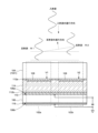
- 5 shows a state in which a voltage is applied between a patch electrode and a common electrode when a reflector unit cell used in a radio wave reflector according to an embodiment of the present invention operates. The results of measuring the reflection amplitude with respect to the distance between the common electrode and the metal film of the radio wave reflection device according to this example are shown.
- 1 shows a cross-sectional structure of a reflector unit cell of a radio wave reflecting device according to an embodiment of the present invention.
- 1 shows a cross-sectional structure of a reflector unit cell of a radio wave reflecting device according to an embodiment of the present invention.
- 1 shows a configuration of a radio wave reflecting device according to an embodiment of the present invention.
- 2 schematically shows that the traveling direction of reflected waves changes by the radio wave reflecting device according to an embodiment of the present invention.
- 1 shows a configuration of a radio wave reflecting device according to an embodiment of the present invention.
- 1 shows a cross-sectional structure of a reflector unit cell in a radio wave reflecting device according to an embodiment of the present invention.
- a member or region when a member or region is said to be “above (or below)" another member or region, it means that it is directly above (or directly below) the other member or region unless otherwise specified. This includes not only the case where the item is located above (or below) another member or area, that is, the case where another component is included in between above (or below) the other member or area. .
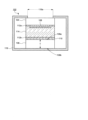
- FIGS. 1A and 1B show a reflector unit cell 102 used in a radio wave reflecting device according to an embodiment of the present invention.
- FIG. 1A shows a plan view of the reflector unit cell 102 viewed from above (the side where radio waves are incident), and
- FIG. 1B shows a cross-sectional view along A1-A2 shown in the plan view.
- the reflector unit cell 102 includes a substrate 104, a substrate 106, a patch electrode 108, a common electrode 110, a first alignment film 112a, a second alignment film 112b, a liquid crystal layer 114, and a metal film 116.
- Patch electrode 108 is provided on substrate 104 and common electrode 110 is provided on substrate 106.
- Patch electrode 108 and common electrode 110 are arranged to face each other, and liquid crystal layer 114 is arranged between patch electrode 108 and common electrode 110.
- a first alignment film 112a is provided on the substrate 104 between the patch electrode 108 and the liquid crystal layer 114, and a second alignment film 112b is provided on the substrate 106 between the common electrode 110 and the liquid crystal layer 114.
- the substrate 106 has a first surface 106a and a second surface 106b opposite to the first surface 106a.
- a common electrode 110 is provided on the first surface 106a
- a metal film 116 is provided on the second surface 106b.
- the metal film 116 is disposed on the opposite side of the common electrode 110 from the liquid crystal layer 114 side, and is disposed away from the common electrode 110.
- T is the distance between the first surface 106a and the second surface 106b and/or the distance between the common electrode 110 and the metal film 116.
- the metal film 116 is arranged to overlap with the patch electrode 108 and is formed to have the same or larger area than the common electrode 110.
- the patch electrode 108 preferably has a shape that is symmetrical with respect to the vertically polarized wave and the horizontally polarized wave of the irradiated radio wave, and has a square or circular shape in plan view.
- FIG. 1A shows a case where the patch electrode 108 is square in plan view.
- the shape of the common electrode 110 is not particularly limited, and has a shape that spreads over the substrate 106 so as to have a larger area than the patch electrode 108.
- the material used for the patch electrode 108 and the common electrode 110 is, for example, a conductive metal, a metal oxide film, or the like.
- a first wiring 118 may be provided on the substrate 104 and is directly or electrically connected to the patch electrode 108.
- the first wiring 118 can be used when applying a control signal to the patch electrode 108. Further, the first wiring 118 can be used, for example, when connecting a patch electrode 108 to an adjacent patch electrode 108 when a plurality of reflector unit cells are arranged.
- the substrate 104 and the substrate 106 are bonded together using a sealant.
- the distance between the substrate 104 and the substrate 106 is 20 to 100 ⁇ m, for example, 50 ⁇ m.
- a patch electrode 108, a common electrode 110, a first alignment film 112a, and a second alignment film 112b are provided between the substrate 104 and the substrate 106.
- the distance between the first alignment film 112a and the second alignment film 112b is the thickness of the liquid crystal layer 114.
- a spacer may be provided between the substrate 104 and the substrate 106 to keep the distance constant.
- a control signal for controlling the orientation of liquid crystal molecules in the liquid crystal layer 114 is applied to the patch electrode 108.
- the metal electrode 116 is supplied with a potential independently of the supply of these signals and is in a floating state.
- the control signal is a DC voltage signal or a polarity inversion signal in which a positive DC voltage and a negative DC voltage are alternately inverted.
- the common electrode 110 is applied with a voltage at an intermediate level of ground or a polarity inverted signal.
- liquid crystal layer 114 nematic liquid crystal, smectic liquid crystal, cholesteric liquid crystal, or discotic liquid crystal can be used as the liquid crystal layer 114.
- the dielectric constant of the liquid crystal layer 114 having dielectric anisotropy changes due to changes in the alignment state of liquid crystal molecules.
- the reflector unit cell 102 can change the dielectric constant of the liquid crystal layer 114 by a control signal applied to the patch electrode 108, thereby delaying the phase of the reflected wave when reflecting the radio wave.
- the frequency bands of the radio waves reflected by the reflector unit cell 102 include the very high frequency (VHF) band, the ultra-high frequency (UHF) band, the microwave (SHF: super high frequency) band, and the sub-band.
- THF Tremendously high frequency
- EHF Extra High Frequency
- FIG. 2A shows a state in which no voltage is applied between the patch electrode 108 and the common electrode 110 (referred to as a "first state"). At this time, the metal film 116 is in a floating state.
- FIG. 2A shows a case where the first alignment film 112a and the second alignment film 112b are horizontal alignment films. The long axes of the liquid crystal molecules 114a in the first state are aligned horizontally with respect to the surfaces of the patch electrode 108 and the common electrode 110 by the first alignment film 112a and the second alignment film 112b.
- FIG. 2B shows a state in which a control signal (voltage signal) is applied to the patch electrode 108 (referred to as a "second state").
- the metal film 116 is in a floating state.
- the long axes of the liquid crystal molecules 114a are aligned perpendicular to the surfaces of the patch electrode 108 and the common electrode 110 under the action of the electric field.
- the angle at which the long axis of the liquid crystal molecules 114a is oriented is determined by the magnitude of the control signal applied to the patch electrode 108 (the magnitude of the voltage between the counter electrode and the patch electrode), so that the liquid crystal molecules 114a are oriented in a direction intermediate between the horizontal direction and the vertical direction. You can also do that.
- the dielectric constant is larger in the second state than in the first state. Further, when the liquid crystal molecules 114a have negative dielectric constant anisotropy, the apparent dielectric constant in the second state is smaller than that in the first state.
- the liquid crystal layer 114 having dielectric constant anisotropy can also be regarded as a variable dielectric layer.
- the reflector unit cell 102 can be controlled to delay (or not delay) the phase of the reflected wave by utilizing the dielectric anisotropy of the liquid crystal layer 114.
- the reflector unit cell 102 is used as a reflector that reflects radio waves in a predetermined direction.
- the reflector unit cell 102 preferably has a high reflected wave amplitude (reflection amplitude), and preferably completely reflects the radio waves irradiated onto the reflector unit cell 102.
- the common electrode 110 has a role of reflecting the radio waves irradiated to the patch electrode 108, the common electrode 110 may not be able to completely reflect the irradiated radio waves.
- a metal film 116 is provided on the opposite side of the common electrode 110 from the liquid crystal layer 114. Further, the metal film 116 is placed apart from the common electrode 110. By arranging the metal film 116 in this manner, the metal film 116 can reflect radio waves that cannot be reflected by the common electrode 110. Therefore, the reflector unit cell 102 can expand the amplitude of the reflected wave.
- the substrate 106 can be provided between the common electrode 110 and the metal film 116, and the common electrode 110 can be provided on the liquid crystal layer 114 side of the substrate 106, and the metal film 116 can be provided on the opposite side. Accordingly, the substrate 106 is shown in FIG. 1B, where the distance T can indicate the thickness of the substrate 106, and the thickness of the substrate 106 also needs to be considered as described above.
- FIG. 3 shows the results of measuring the reflection amplitude with respect to the distance T between the common electrode 110 and the metal film 116.
- cells 1 to 3 having the configuration of the reflector unit cell 102 shown in FIG. 1B were used.
- Aluminum with a thickness of 1.0 ⁇ m was used for the patch electrodes 108 and common electrodes 110 of cells 1 to 3
- aluminum (Al) with a thickness of 1.0 ⁇ m was used for the metal film 116.
- the size of the patch electrode 108 was 2.80 mm square for cell 1, 2.85 mm square for cell 2, and 2.90 mm square for cell 3, respectively.
- Glass substrates were used for the substrate 104 and the substrate 106.
- the radio waves irradiated to the patch electrodes of cells 1 to 3 had a wavelength ( ⁇ ) of 10.7 mm in air with a frequency of 28 GHz.
- x is the value obtained by multiplying the distance T between the common electrode 110 and the metal film 116 by the wavelength ⁇ of the radio wave irradiated to the patch electrode 108, that is, the distance T ⁇ .
- FIG. 5 shows an example in which the frame 119 holding the reflector unit cell 102 has the function of the metal film 116. Specifically, an example will be shown in which a frame 119 made of a material that reflects radio waves is provided in the reflector unit cell 102 so as to face the substrate 106.
- the radio wave reflecting device 100a when using the frame 119 in the radio wave reflecting devices 100a and 100b, which will be described later, a plurality of reflector unit cells 102 are used, but instead of providing an opening 119a in each of the reflector unit cells 102, the radio wave reflecting device 100a Depending on the size of the reflector unit cells 102 or 100b, one may be provided for each of a certain number of reflector unit cells 102. However, the number of openings 119a is not limited.
- the step of forming the metal film 116 can be omitted in the manufacturing process of the radio wave reflecting device 100. Further, by providing the frame 119 having a thickness equal to or greater than the thickness of the metal film 116, it is possible to easily obtain the amplitude of the reflected wave equal to or greater than that of the metal film 116.
- the metal film 116 may be provided on a substrate 117 different from the substrate 106 on which the common electrode 110 is provided, or the frame 119 having radio wave reflective properties may be provided so that the metal film 116 or the frame 119 faces the substrate 106. Then, the frame 119 can be retrofitted to the reflector unit cell 102. These retrofits can simplify the process of manufacturing the reflector unit cell 102 and shorten the time.
- Radio Wave Reflector Next, the configuration of a radio wave reflector in which reflector units are integrated will be shown.
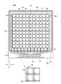
- FIG. 6 shows the configuration of a radio wave reflecting device 100a according to an embodiment of the present invention.
- the radio wave reflection device 100a has a reflection plate 120.
- the reflector 120 is composed of a plurality of reflector unit cells 102.
- the plurality of reflector unit cells 102 are arranged, for example, in a first direction (X-axis direction shown in FIG. 6) and a second direction (Y-axis direction shown in FIG. 6) intersecting the first direction.
- the reflector unit cell 102 is arranged so that the patch electrode 108 faces the radio wave incident surface.
- the reflecting plate 120 has a flat plate shape, and a plurality of patch electrodes 108 are arranged in a matrix within the flat plane.
- the radio wave reflecting device 100 has a structure in which a plurality of reflector unit cells 102 are integrated on one substrate 104. As shown in FIG. 6, the radio wave reflecting device 100 has a substrate 104 on which a plurality of patch electrodes 108 are arranged, and a substrate 106 on which a common electrode 110 and a metal film 116 are provided, which are arranged one on top of the other, and between the two substrates. It has a structure in which a liquid crystal layer (not shown) is provided on the top. At this time, the surface of the substrate 106 on which the common electrode 110 is provided faces the liquid crystal layer (not shown).
- the reflective plate 120 is formed in a region where the plurality of patch electrodes 108, the common electrode 110, and the metal film 116 overlap.
- the cross-sectional structure of the reflector 120 is the same as the structure of the reflector unit cell 102 shown in FIG. 1B when looking at the individual patch electrodes 108.
- the metal film 116 is arranged inside the sealing material 128 and overlaps with the reflecting plate 120 in a plan view, but it may be provided wider than the reflecting plate 120 and in an overlapping manner. It may be provided so as to spread outward from the sealing material 128.
- the substrate 104 and the substrate 106 are bonded together with a sealant 128, and a liquid crystal layer (not shown) is provided in an area inside the sealant 128.
- a frame 119 (not shown) can be provided as shown in FIG.
- the frame 119 is provided so that the reflector 120 is exposed, and the opening 119a of the frame 119 overlaps with the reflector 120.
- a frame 119 (not shown) can be provided to protect and hold a structure mounted on the radio wave reflecting device 100a.
- a frame 119 (not shown) surrounds the substrate 104 and the substrate 106, and is arranged to sandwich the substrate 104 and the substrate 106 in a cross-sectional view. At this time, one or more openings 119a of the frame 119 may be provided depending on the size of the radio wave reflecting device 100a or the patch electrode 108.
- a plurality of patch electrodes 108 are arranged on the substrate 104 in the first direction (X-axis direction) and the second direction (Y-axis direction). Further, a plurality of first wirings 118 extending in the second direction (Y-axis direction) are arranged on the substrate 104. Each of the plurality of first wirings 118 is electrically connected to the plurality of patch electrodes 108 arranged in the second direction (Y-axis direction). In other words, the plurality of patch electrodes 108 arranged in the second direction (Y-axis direction) are connected by the first wiring 118.
- the reflecting plate 120 has a configuration in which a plurality of patch electrode arrays are arranged in a first direction (X-axis direction) in a row connected by first wiring 118.
- a plurality of first wirings 118 arranged on the reflection plate 120 extend to the peripheral region 122 and are connected to the first drive circuit 124.
- the first drive circuit 124 outputs a control signal to be applied to the patch electrode 108.
- the first drive circuit 124 can output control signals of different voltage levels to each of the plurality of first wirings 118.
- the plurality of patch electrodes 108 arranged in the first direction (X-axis direction) and the second direction (Y-axis direction) are arranged column by column (in the second direction (Y-axis direction)).
- a control signal is applied to each patch electrode 108).
- a control signal is applied to each set of a plurality of patch electrodes 108 arranged in a second direction (Y-axis direction), thereby controlling the reflection direction of the reflected radio waves incident on the reflection plate 120.
- the radio wave reflecting device 100a can control the propagation direction of the reflected waves in the horizontal direction in the drawing centering on the reflection axis VR parallel to the second direction (Y-axis direction). can.
- FIG. 7 schematically shows that the traveling direction of reflected waves changes due to the two reflector unit cells 102.
- different control signals V1 ⁇ V2
- V1 ⁇ V2 different control signals
- the phase change of the wave reflected by the second reflector unit cell 102b is larger than that of the first reflector unit cell 102a.
- the phase of the reflected wave R1 reflected by the first reflector unit cell 102a and the phase of the reflected wave R2 reflected by the second reflector unit cell 102b are different (in FIG. 7, the phase of the reflected wave R2 is different from the phase of the reflected wave R1). ), the traveling direction of the reflected wave appears to change diagonally.
- the plurality of patch electrodes 108 arranged in the second direction are electrically connected by the first wiring 118 and have an electrically equal potential, so that the shape is divided into a plurality of parts.
- the dimensions of the patch electrode 108 have an appropriate range depending on the wavelength of the reflected radio waves, so if the electrode is shaped like a strip, the sensitivity to the target wavelength will decrease, and the behavior for vertically polarized waves and horizontally polarized waves will differ. Put it away. Therefore, as shown in FIG.
- FIG. 8 shows the configuration of a radio wave reflection device 100b according to this embodiment.
- the parts that are different from the radio wave reflecting device 100a shown in FIG. 5 will be mainly explained.
- first connection wiring 144 is provided in the same layer as the conductive layer forming the first wiring 118.
- the first connection wiring 144 is provided so as to be in contact with the semiconductor layer 142.
- the connection structure of the first wiring 118 and the first connection wiring 144 to the semiconductor layer 142 shows a structure in which one wiring is connected to the source of the transistor and the other wiring is connected to the drain.
- the undercoat layer 136 is formed of, for example, a silicon oxide film.
- the first gate insulating layer 140 and the second gate insulating layer 146 are formed of, for example, a silicon oxide film or a laminated structure of a silicon oxide film and a silicon nitride film.
- the semiconductor layer is formed of a silicon semiconductor such as amorphous silicon or polycrystalline silicon, or an oxide semiconductor containing a metal oxide such as indium oxide, zinc oxide, or gallium oxide.
- the first gate electrode 138 and the second gate electrode 148 may be made of, for example, molybdenum (Mo), tungsten (W), or an alloy thereof.
- the first wiring 118, the second wiring 132, the first connection wiring 144, and the second connection wiring 152 are formed using a metal material such as titanium (Ti), aluminum (Al), or molybdenum (Mo).
- a metal material such as titanium (Ti), aluminum (Al), or molybdenum (Mo).
- it may have a laminated structure of titanium (Ti)/aluminum (Al)/titanium (Ti) or a laminated structure of molybdenum (Mo)/aluminum (Al)/molybdenum (Mo).
- the planarization layer 156 is made of a resin material such as acrylic or polyimide.
- the passivation layer 158 is formed of, for example, a silicon nitride film.
- the patch electrode 108 and the common electrode 110 are formed of a metal film such as aluminum (Al) or copper (Cu), or a transparent conductive film such as indium tin oxide (ITO).
- the second wiring 132 is connected to the gate of the transistor used as the switching element 134
- the first wiring 118 is connected to one of the source and drain of the transistor
- the patch electrode 108 is connected to the other of the source and drain.
- a control signal can be applied to a predetermined patch electrode selected from among the plurality of patch electrodes 108 arranged in a matrix.
- a control voltage can be applied to each patch electrode 108 arranged in a vertical line along the axial direction. can be controlled.
- the radio wave reflecting device 100 has the metal film 116 formed on the side opposite to the liquid crystal layer of the common electrode 110 forming the reflecting plate 120, By setting the value obtained by multiplying the distance T between the metal film 116 and the wavelength ⁇ of the radio waves irradiated to the patch electrode 108 to 0.02 or more and 0.34 or less, or 0.10 or more and 0.22 or less, reflection can be reduced. Gain can be increased.
- radio wave reflecting device and the reflecting plate unit illustrated as an embodiment of the present invention can be appropriately combined as long as they do not contradict each other.
- those skilled in the art may appropriately add, delete, or change the design of components, or add, omit, or condition a process. Modifications are also included within the scope of the present invention as long as they have the gist of the present invention.
Abstract
This radio wave reflection device is provided with a patch electrode, a common electrode, a liquid crystal layer sandwiched between the patch electrode and the common electrode, and a metal film disposed on the opposite side of the common electrode from the liquid crystal layer side, wherein the metal film is disposed to be separate from the common electrode and the patch electrode is disposed to overlap the metal film. Provided that a value obtained by multiplying the distance T between the common electrode and the metal film by a wavelength λ of a radio wave radiated to the patch electrode is x, x may be 0.02-0.34. Further, x may be 0.10-0.22.
Description
本発明の実施形態の一つは、電波反射装置に関する。
One embodiment of the present invention relates to a radio wave reflecting device.
電気的に指向性を制御できるフェーズドアレイアンテナ(Phased Array Antenna)装置に使用する移相器として、液晶を利用した移相器の開発が行われている(特許文献1および特許文献2参照)。
A phase shifter using liquid crystal is being developed as a phase shifter for use in a phased array antenna device whose directivity can be electrically controlled (see Patent Document 1 and Patent Document 2).
フェーズドアレイアンテナ装置では、移相器が接続されたアンテナ素子を1次元または2次元で並べられており、隣り合ったアンテナ素子に入力する信号の位相差を一定となるように液晶の誘電率を調整する必要がある。また、液晶を利用して反射方向を制御できる反射板の検討も行われている。この反射板も反射電極(パッチ電極)が1次元または2次元方向に並べた構造であり、各電極部の液晶誘電率を電圧により調整して反射位相を制御することで電波の反射方向を任意の方向に設定ができる。反射板の反射振幅は高い方が好ましいが、液晶を用いた反射板では反射振幅が小さいという問題がある。
In a phased array antenna device, antenna elements connected to phase shifters are arranged in one or two dimensions, and the dielectric constant of the liquid crystal is adjusted so that the phase difference between signals input to adjacent antenna elements is constant. Need to adjust. Further, studies are being conducted on a reflector plate that can control the direction of reflection using liquid crystals. This reflector also has a structure in which reflective electrodes (patch electrodes) are arranged in one or two dimensions, and by adjusting the liquid crystal permittivity of each electrode part with voltage and controlling the reflection phase, the direction of reflection of radio waves can be set arbitrarily. It can be set in the direction of Although it is preferable for the reflection plate to have a high reflection amplitude, a reflection plate using liquid crystal has a problem in that the reflection amplitude is small.
このような問題に鑑み本発明の一実施形態は、新規な構造を有する電波反射装置を提供することを課題の一つとする。また、反射利得の高い電波反射装置を提供することを目的の一つとする。
In view of such problems, one of the objects of an embodiment of the present invention is to provide a radio wave reflection device having a novel structure. Another object of the present invention is to provide a radio wave reflecting device with high reflection gain.
本発明の一実施形態に係る電波反射装置は、パッチ電極と、コモン電極と、パッチ電極とコモン電極に挟まれる液晶層と、コモン電極の液晶層側とは反対側に配置される金属膜と、を有し、金属膜は、コモン電極と離れて配置され、パッチ電極は金属膜と重なるように配置される。
A radio wave reflecting device according to an embodiment of the present invention includes a patch electrode, a common electrode, a liquid crystal layer sandwiched between the patch electrode and the common electrode, and a metal film disposed on the side opposite to the liquid crystal layer of the common electrode. , the metal film is placed apart from the common electrode, and the patch electrode is placed so as to overlap the metal film.
以下、本発明の実施の形態を、図面などを参照しながら説明する。但し、本発明は多くの異なる態様で実施することが可能であり、以下に例示する実施の形態の記載内容に限定して解釈されるものではない。図面は説明をより明確にするため、実際の態様に比べ、各部の幅、厚さ、形状などについて模式的に表される場合があるが、あくまで一例であって、本発明の解釈を限定するものではない。また、本明細書と各図において、既出の図に関して前述したものと同様の要素には、同一の符号(又は数字の後にa、bなどを付した符号)を付して、詳細な説明を適宜省略することがある。さらに各要素に対する「第1」、「第2」と付記された文字は、各要素を区別するために用いられる便宜的な標識であり、特段の説明がない限りそれ以上の意味を有しない。
Embodiments of the present invention will be described below with reference to the drawings and the like. However, the present invention can be implemented in many different modes, and should not be construed as being limited to the contents of the embodiments exemplified below. In order to make the explanation more clear, the drawings may schematically represent the width, thickness, shape, etc. of each part compared to the actual aspect, but this is just an example and does not limit the interpretation of the present invention. It's not a thing. In addition, in this specification and each drawing, elements similar to those described above with respect to the existing drawings are denoted by the same reference numerals (or numerals followed by a, b, etc.) and detailed explanations are given. It may be omitted as appropriate. Furthermore, the characters ``first'' and ``second'' for each element are convenient signs used to distinguish each element, and have no further meaning unless otherwise specified.
本明細書において、ある部材又は領域が他の部材又は領域の「上に(又は下に)」あるとする場合、特段の限定がない限りこれは他の部材又は領域の直上(又は直下)にある場合のみでなく他の部材又は領域の上方(又は下方)にある場合を含み、すなわち、他の部材又は領域の上方(又は下方)において間に別の構成要素が含まれている場合も含む。
In this specification, when a member or region is said to be "above (or below)" another member or region, it means that it is directly above (or directly below) the other member or region unless otherwise specified. This includes not only the case where the item is located above (or below) another member or area, that is, the case where another component is included in between above (or below) the other member or area. .
<第1実施形態>
1.反射板ユニットセル
図1A及びBは、本発明の一実施形態に係る電波反射装置に用いられる反射板ユニットセル102を示す。図1Aは、反射板ユニットセル102を上方(電波が入射する側)からみたときの平面図を示し、図1Bは平面図に示すA1-A2間の断面図を示す。 <First embodiment>
1. Reflector Unit Cell FIGS. 1A and 1B show areflector unit cell 102 used in a radio wave reflecting device according to an embodiment of the present invention. FIG. 1A shows a plan view of the reflector unit cell 102 viewed from above (the side where radio waves are incident), and FIG. 1B shows a cross-sectional view along A1-A2 shown in the plan view.
1.反射板ユニットセル
図1A及びBは、本発明の一実施形態に係る電波反射装置に用いられる反射板ユニットセル102を示す。図1Aは、反射板ユニットセル102を上方(電波が入射する側)からみたときの平面図を示し、図1Bは平面図に示すA1-A2間の断面図を示す。 <First embodiment>
1. Reflector Unit Cell FIGS. 1A and 1B show a
図1A及びBに示すように、反射板ユニットセル102は、基板104と基板106、パッチ電極108、コモン電極110、第1配向膜112a、第2配向膜112b、液晶層114、金属膜116を含む。パッチ電極108は、基板104に設けられ、コモン電極110は、基板106に設けられる。パッチ電極108とコモン電極110は対向するように配置され、パッチ電極108とコモン電極110に挟まれる液晶層114が配置される。パッチ電極108と液晶層114との間に第1配向膜112aが基板104に設けられ、コモン電極110と液晶層114との間に第2配向膜112bが基板106に設けられる。
As shown in FIGS. 1A and 1B, the reflector unit cell 102 includes a substrate 104, a substrate 106, a patch electrode 108, a common electrode 110, a first alignment film 112a, a second alignment film 112b, a liquid crystal layer 114, and a metal film 116. include. Patch electrode 108 is provided on substrate 104 and common electrode 110 is provided on substrate 106. Patch electrode 108 and common electrode 110 are arranged to face each other, and liquid crystal layer 114 is arranged between patch electrode 108 and common electrode 110. A first alignment film 112a is provided on the substrate 104 between the patch electrode 108 and the liquid crystal layer 114, and a second alignment film 112b is provided on the substrate 106 between the common electrode 110 and the liquid crystal layer 114.
基板106は、第1面106aと第1面106aとは反対に第2面106bを有する。第1面106aには、コモン電極110が設けられ、第2面106bには、金属膜116が設けられる。金属膜116は、コモン電極110の液晶層114側とは反対側に配置され、また、コモン電極110と離れて配置される。このとき、第1面106aと第2面106bとの間の距離および/またはコモン電極110と金属膜116との間の距離をTとする。また、金属膜116は、パッチ電極108と重なるように配置され、コモン電極110と同じまたはそれより広い面積を有するように形成されている。
The substrate 106 has a first surface 106a and a second surface 106b opposite to the first surface 106a. A common electrode 110 is provided on the first surface 106a, and a metal film 116 is provided on the second surface 106b. The metal film 116 is disposed on the opposite side of the common electrode 110 from the liquid crystal layer 114 side, and is disposed away from the common electrode 110. At this time, T is the distance between the first surface 106a and the second surface 106b and/or the distance between the common electrode 110 and the metal film 116. Furthermore, the metal film 116 is arranged to overlap with the patch electrode 108 and is formed to have the same or larger area than the common electrode 110.
パッチ電極108は、照射される電波の垂直偏波および水平偏波に対して対称となる形状を有していることが好ましく、平面視で正方形または円形の形状を有する。図1Aは、パッチ電極108が平面視で正方形である場合を示す。コモン電極110の形状には特に制限はなく、パッチ電極108より広い面積を有するように基板106に広がる形状を有する。パッチ電極108およびコモン電極110に用いる材料は、例えば、導電性を有する金属、金属酸化膜等を用いて形成される。
The patch electrode 108 preferably has a shape that is symmetrical with respect to the vertically polarized wave and the horizontally polarized wave of the irradiated radio wave, and has a square or circular shape in plan view. FIG. 1A shows a case where the patch electrode 108 is square in plan view. The shape of the common electrode 110 is not particularly limited, and has a shape that spreads over the substrate 106 so as to have a larger area than the patch electrode 108. The material used for the patch electrode 108 and the common electrode 110 is, for example, a conductive metal, a metal oxide film, or the like.
また、基板104には、第1配線118が設けられてもよく、パッチ電極108と直接または電気的に接続される。第1配線118は、パッチ電極108に制御信号を印加するときに用いることができる。また、第1配線118は、複数の反射板ユニットセルが配列する場合、例えば、パッチ電極108とそれに隣接するパッチ電極108とを接続するときに用いることができる。
Further, a first wiring 118 may be provided on the substrate 104 and is directly or electrically connected to the patch electrode 108. The first wiring 118 can be used when applying a control signal to the patch electrode 108. Further, the first wiring 118 can be used, for example, when connecting a patch electrode 108 to an adjacent patch electrode 108 when a plurality of reflector unit cells are arranged.
図1AおよびBには示されないが、基板104と基板106とは、シール材により貼り合わされる。このとき、基板104と基板106との間隔は20~100μmであり、例えば、50μmの間隔を有する。基板104と基板106との間には、パッチ電極108、コモン電極110、第1配向膜112a、第2配向膜112bが設けられるため、正確には基板104と基板106の各々に設けられた第1配向膜112a及び第2配向膜112bの間の間隔が液晶層114の厚さとなる。なお、図1Bには図示されないが、基板104と基板106との間には間隔を一定に保つためのスペーサが設けられていてもよい。
Although not shown in FIGS. 1A and 1B, the substrate 104 and the substrate 106 are bonded together using a sealant. At this time, the distance between the substrate 104 and the substrate 106 is 20 to 100 μm, for example, 50 μm. A patch electrode 108, a common electrode 110, a first alignment film 112a, and a second alignment film 112b are provided between the substrate 104 and the substrate 106. The distance between the first alignment film 112a and the second alignment film 112b is the thickness of the liquid crystal layer 114. Note that although not shown in FIG. 1B, a spacer may be provided between the substrate 104 and the substrate 106 to keep the distance constant.
パッチ電極108には液晶層114の液晶分子の配向を制御する制御信号が印加される。金属電極116は、これら信号の供給とは独立して電位が供給され、フローティング状態である。制御信号は直流電圧の信号、または正の直流電圧と負の直流電圧が交互に反転する極性反転信号である。コモン電極110は、接地または極性反転信号の中間レベルの電圧が印加される。パッチ電極108に制御信号が印加されることで液晶層114に含まれる液晶分子の配向状態が変化する。液晶層114には誘電率異方性を有する液晶材料が用いられる。例えば、液晶層114として、ネマチック液晶、スメクチック液晶、コレステリック液晶、ディスコティック液晶を用いることができる。誘電率異方性を有する液晶層114は、液晶分子の配向状態の変化により誘電率が変化する。反射板ユニットセル102は、パッチ電極108に印加する制御信号によって液晶層114の誘電率を変化させることができ、それによって電波を反射するときに反射波の位相を遅延させることができる。
A control signal for controlling the orientation of liquid crystal molecules in the liquid crystal layer 114 is applied to the patch electrode 108. The metal electrode 116 is supplied with a potential independently of the supply of these signals and is in a floating state. The control signal is a DC voltage signal or a polarity inversion signal in which a positive DC voltage and a negative DC voltage are alternately inverted. The common electrode 110 is applied with a voltage at an intermediate level of ground or a polarity inverted signal. By applying a control signal to the patch electrode 108, the alignment state of liquid crystal molecules included in the liquid crystal layer 114 changes. A liquid crystal material having dielectric constant anisotropy is used for the liquid crystal layer 114. For example, as the liquid crystal layer 114, nematic liquid crystal, smectic liquid crystal, cholesteric liquid crystal, or discotic liquid crystal can be used. The dielectric constant of the liquid crystal layer 114 having dielectric anisotropy changes due to changes in the alignment state of liquid crystal molecules. The reflector unit cell 102 can change the dielectric constant of the liquid crystal layer 114 by a control signal applied to the patch electrode 108, thereby delaying the phase of the reflected wave when reflecting the radio wave.
反射板ユニットセル102が反射する電波の周波数帯は、超短波(VHF:Very High Frequency)帯、極超短波(UHF:Ultra-High Frequency)帯、マイクロ波(SHF:Super HighFrequency)帯、サブミリ波(THF:Tremendously high frequency)、ミリ波(EHF:Extra High Frequency)帯である。液晶層114の液晶分子はパッチ電極108に印加される制御信号に応答して液晶分子の配向が変化するが、パッチ電極108に照射される電波の周波数にはほとんど追従しない。したがって、反射板ユニットセル102は、電波の影響を受けずに反射する電波の位相を制御することができる。
The frequency bands of the radio waves reflected by the reflector unit cell 102 include the very high frequency (VHF) band, the ultra-high frequency (UHF) band, the microwave (SHF: super high frequency) band, and the sub-band. Millimeter wave (THF : Tremendously high frequency), millimeter wave (EHF: Extra High Frequency) band. Although the orientation of the liquid crystal molecules in the liquid crystal layer 114 changes in response to the control signal applied to the patch electrode 108, it hardly follows the frequency of the radio waves applied to the patch electrode 108. Therefore, the reflector unit cell 102 can control the phase of the reflected radio waves without being influenced by the radio waves.
図2Aは、パッチ電極108とコモン電極110との間に電圧が印加されない状態(「第1の状態」とする)を示す。このとき、金属膜116は、フローティング状態である。図2Aは、第1配向膜112a及び第2配向膜112bが水平配向膜である場合を示す。第1の状態における液晶分子114aの長軸は、第1配向膜112a及び第2配向膜112bによりパッチ電極108及びコモン電極110の表面に対して水平に配向している。図2Bは、パッチ電極108に制御信号(電圧信号)が印加された状態(「第2の状態」とする)を示す。ここでも、金属膜116は、フローティング状態である。第2の状態において、液晶分子114aは電界の作用を受けて長軸がパッチ電極108及びコモン電極110の表面に対し垂直に配向する。液晶分子114aの長軸が配向する角度は、パッチ電極108に印加する制御信号の大きさ(対向電極とパッチ電極間の電圧の大きさ)によって、水平方向と垂直方向の中間の方向に配向させることもできる。
FIG. 2A shows a state in which no voltage is applied between the patch electrode 108 and the common electrode 110 (referred to as a "first state"). At this time, the metal film 116 is in a floating state. FIG. 2A shows a case where the first alignment film 112a and the second alignment film 112b are horizontal alignment films. The long axes of the liquid crystal molecules 114a in the first state are aligned horizontally with respect to the surfaces of the patch electrode 108 and the common electrode 110 by the first alignment film 112a and the second alignment film 112b. FIG. 2B shows a state in which a control signal (voltage signal) is applied to the patch electrode 108 (referred to as a "second state"). Here too, the metal film 116 is in a floating state. In the second state, the long axes of the liquid crystal molecules 114a are aligned perpendicular to the surfaces of the patch electrode 108 and the common electrode 110 under the action of the electric field. The angle at which the long axis of the liquid crystal molecules 114a is oriented is determined by the magnitude of the control signal applied to the patch electrode 108 (the magnitude of the voltage between the counter electrode and the patch electrode), so that the liquid crystal molecules 114a are oriented in a direction intermediate between the horizontal direction and the vertical direction. You can also do that.
液晶分子114aが正の誘電率異方性を有する場合、第1の状態に対して第2の状態の方が、誘電率が大きくなる。また、液晶分子114aが負の誘電率異方性を有する場合、第1の状態に対して第2の状態の方が見かけ上の誘電率が小さくなる。誘電率異方性を有する液晶層114は、可変誘電体層とみなすこともできる。反射板ユニットセル102は、液晶層114の誘電率異方性を利用して、反射波の位相を遅らせる(又は遅らせない)ように制御することができる。
When the liquid crystal molecules 114a have positive dielectric constant anisotropy, the dielectric constant is larger in the second state than in the first state. Further, when the liquid crystal molecules 114a have negative dielectric constant anisotropy, the apparent dielectric constant in the second state is smaller than that in the first state. The liquid crystal layer 114 having dielectric constant anisotropy can also be regarded as a variable dielectric layer. The reflector unit cell 102 can be controlled to delay (or not delay) the phase of the reflected wave by utilizing the dielectric anisotropy of the liquid crystal layer 114.
反射板ユニットセル102は、電波を所定の方向に反射する反射板に用いられる。反射板ユニットセル102は、反射波の振幅(反射振幅)が高い方が好ましく、反射板ユニットセル102に照射された電波を完全に反射することが好ましい。しかし、コモン電極110は、パッチ電極108に照射された電波を反射する役割があるが、コモン電極110がその照射された電波を完全には反射しきれない場合がある。ここで、図1Bに示す構造のように、コモン電極110の液晶層114とは反対側に金属膜116を設ける。また、金属膜116をコモン電極110と離して配置する。このように金属膜116を配置することで、コモン電極110で反射しきれない電波を金属膜116で反射することができる。したがって、反射板ユニットセル102は、反射波の振幅を拡大することができる。
The reflector unit cell 102 is used as a reflector that reflects radio waves in a predetermined direction. The reflector unit cell 102 preferably has a high reflected wave amplitude (reflection amplitude), and preferably completely reflects the radio waves irradiated onto the reflector unit cell 102. However, although the common electrode 110 has a role of reflecting the radio waves irradiated to the patch electrode 108, the common electrode 110 may not be able to completely reflect the irradiated radio waves. Here, as in the structure shown in FIG. 1B, a metal film 116 is provided on the opposite side of the common electrode 110 from the liquid crystal layer 114. Further, the metal film 116 is placed apart from the common electrode 110. By arranging the metal film 116 in this manner, the metal film 116 can reflect radio waves that cannot be reflected by the common electrode 110. Therefore, the reflector unit cell 102 can expand the amplitude of the reflected wave.
さらに、図1Bに示す構造のように、コモン電極110の液晶層114側とは反対側にある一定の距離Tを離して金属膜116を設ける。このように金属膜116を設けることで、コモン電極110で反射しきれない電波を金属膜116で反射することができる。ただし、パッチ電極108に照射された電波はコモン電極110または金属膜116にて反射されるため、コモン電極110で反射した電波と金属膜116で反射した電波の反射波の振幅が減衰しないように、コモン電極110と金属膜116との距離Tを検討する必要がある。また、コモン電極110と金属膜116との間には、基板106を設けることができ、基板106の液晶層114側にコモン電極110、その反対側に金属膜116を設けることができる。したがって、基板106は、図1Bで示すように、距離Tは基板106の厚さを示すことができ、また、上述したように基板106の厚さも検討する必要がある。
Further, as in the structure shown in FIG. 1B, a metal film 116 is provided at a certain distance T on the opposite side of the common electrode 110 from the liquid crystal layer 114 side. By providing the metal film 116 in this manner, the metal film 116 can reflect radio waves that cannot be reflected by the common electrode 110. However, since the radio waves irradiated to the patch electrode 108 are reflected by the common electrode 110 or the metal film 116, the amplitude of the reflected waves of the radio waves reflected by the common electrode 110 and the radio waves reflected by the metal film 116 is not attenuated. , it is necessary to consider the distance T between the common electrode 110 and the metal film 116. Further, the substrate 106 can be provided between the common electrode 110 and the metal film 116, and the common electrode 110 can be provided on the liquid crystal layer 114 side of the substrate 106, and the metal film 116 can be provided on the opposite side. Accordingly, the substrate 106 is shown in FIG. 1B, where the distance T can indicate the thickness of the substrate 106, and the thickness of the substrate 106 also needs to be considered as described above.
図3は、コモン電極110と金属膜116との距離Tに対する反射振幅を測定した結果を示す。図3に示す測定結果には、図1Bに示す反射板ユニットセル102の構成を有するセル1~3を用いた。セル1~3のパッチ電極108およびコモン電極110には、膜厚1.0μmアルミニウムを用い、金属膜116には、膜厚1.0μmのアルミニウム(Al)を用いた。パッチ電極108の大きさは、セル1に2.80mm角、セル2に2.85mm角、セル3に2.90mm角をそれぞれ用いた。基板104および基板106には、ガラス基板を用いた。セル1~3のパッチ電極に照射される電波は、周波数28GHzの空気中において波長(λ)10.7mmとした。
FIG. 3 shows the results of measuring the reflection amplitude with respect to the distance T between the common electrode 110 and the metal film 116. For the measurement results shown in FIG. 3, cells 1 to 3 having the configuration of the reflector unit cell 102 shown in FIG. 1B were used. Aluminum with a thickness of 1.0 μm was used for the patch electrodes 108 and common electrodes 110 of cells 1 to 3, and aluminum (Al) with a thickness of 1.0 μm was used for the metal film 116. The size of the patch electrode 108 was 2.80 mm square for cell 1, 2.85 mm square for cell 2, and 2.90 mm square for cell 3, respectively. Glass substrates were used for the substrate 104 and the substrate 106. The radio waves irradiated to the patch electrodes of cells 1 to 3 had a wavelength (λ) of 10.7 mm in air with a frequency of 28 GHz.
ここで、コモン電極110と金属膜116との間の距離Tとパッチ電極108に照射される電波の波長λを掛け合わせた値、距離T×λをxとする。
Here, x is the value obtained by multiplying the distance T between the common electrode 110 and the metal film 116 by the wavelength λ of the radio wave irradiated to the patch electrode 108, that is, the distance T×λ.
セル1~3を、x(距離T×λ)=0.00(距離T=0.00mm)、0.11(距離T=0.50mm)、0.22(距離T=1.00mm)にて、反射波の振幅(dB)をそれぞれ測定した。x=0の測定には、金属膜116が形成されていない反射ユニットセルを用いた。また、反射振幅(反射波の振幅)の測定には、ベクトルネットワークアナライザ(MS46522B、アンリツ社製)により行った。
Cells 1 to 3 are set to x (distance T x λ) = 0.00 (distance T = 0.00 mm), 0.11 (distance T = 0.50 mm), 0.22 (distance T = 1.00 mm) The amplitude (dB) of each reflected wave was measured. For the measurement of x=0, a reflection unit cell on which the metal film 116 was not formed was used. Further, the reflection amplitude (amplitude of reflected wave) was measured using a vector network analyzer (MS46522B, manufactured by Anritsu Corporation).
図3に示すグラフおよび表1から、反射振幅がxに依存して変化することが判る。また、反射振幅は-10dB以上であることが好ましく、図3に示すグラフおよび表1より、x(距離T×λ)が0.11および0.22のとき、セル1~3において-10dB以上の反射振幅が得られることがわかる。また、測定結果より得られるカーブフィッティング(図3に示す点線)から、-10dB以上の反射振幅が得られるxは、0.02以上0.34以下であることがわかる。したがって、xは、0.02以上0.34以下であることが好ましく、さらに、0.10以上0.22以下であることが好ましい。距離Tをこのようなxの範囲にて設定することで、反射板ユニットセル102は、反射波の振幅をさらに拡大することができる。
From the graph shown in FIG. 3 and Table 1, it can be seen that the reflection amplitude changes depending on x. Further, the reflection amplitude is preferably -10 dB or more, and from the graph shown in FIG. It can be seen that a reflection amplitude of is obtained. Further, from the curve fitting (dotted line shown in FIG. 3) obtained from the measurement results, it is found that x for obtaining a reflection amplitude of -10 dB or more is 0.02 or more and 0.34 or less. Therefore, x is preferably 0.02 or more and 0.34 or less, and more preferably 0.10 or more and 0.22 or less. By setting the distance T within such a range of x, the reflector unit cell 102 can further expand the amplitude of the reflected wave.

図4は、金属膜116が、基板117に金属膜116を有する一例を示す。具体的には、基板117が、基板106側に基板104と対向して設けられる例を示す。基板117には、金属膜116が設けられており、基板106と基板117との間に金属膜116が配置されるように貼り合わされる。この貼り合わせにより、基板106に設けられているコモン電極110と基板117に設けられた金属膜116との間の距離Tが基板106の厚さとなる。基板117は、基板104や基板106と同様の基板を用いることができる。
FIG. 4 shows an example in which the metal film 116 has the metal film 116 on the substrate 117. Specifically, an example will be shown in which the substrate 117 is provided on the substrate 106 side facing the substrate 104. A metal film 116 is provided on the substrate 117, and the substrates 106 and 117 are bonded together so that the metal film 116 is disposed between them. Due to this bonding, the distance T between the common electrode 110 provided on the substrate 106 and the metal film 116 provided on the substrate 117 becomes the thickness of the substrate 106. As the substrate 117, the same substrate as the substrate 104 and the substrate 106 can be used.
図4では、基板117に金属膜116を設けた例を示したが、電波反射性を基板117に備えればよく、例えば、アルミニウムやアルミニウム合金のような電波反射性を有する箔等を、金属膜116を設けた基板117の代わりに用いることができる。
Although FIG. 4 shows an example in which the metal film 116 is provided on the substrate 117, it is only necessary to provide the substrate 117 with radio wave reflective properties. It can be used instead of the substrate 117 provided with the film 116.
このように、金属膜116を基板106とは別の基板117に設ける構成を有することで、反射板ユニットセル102の作製工程と同時に金属膜116の形成工程を進めることができるため、反射板ユニットセル102の作製の時間を短縮することができる。
In this way, by having the configuration in which the metal film 116 is provided on the substrate 117 that is different from the substrate 106, the process of forming the metal film 116 can be performed simultaneously with the process of manufacturing the reflector unit cell 102. The time for manufacturing the cell 102 can be shortened.
図5は、反射板ユニットセル102を保持するフレーム119が金属膜116の機能を有する一例を示す。具体的には、反射板ユニットセル102に、電波反射性を有する材料を用いたフレーム119が基板106に直面して設けられる例を示す。
FIG. 5 shows an example in which the frame 119 holding the reflector unit cell 102 has the function of the metal film 116. Specifically, an example will be shown in which a frame 119 made of a material that reflects radio waves is provided in the reflector unit cell 102 so as to face the substrate 106.
図5に示すように、フレーム119は、図5に示すように基板106に直面するように、コモン電極110の液晶層114の反対側に配置される。また、フレーム119は、基板104と基板106を保持している。また、フレーム119は、パッチ電極108の照射される電波とコモン電極110及び金属膜116で反射した電波が通る開口119aが設けられる。開口119aは、図5では、断面視においてパッチ電極108の幅より大きい幅を有する。さらに、後述する電波反射装置100aや100bにフレーム119を用いる場合は、複数の反射板ユニットセル102が用いられるが、反射板ユニットセル102のそれぞれに開口119aを設けるのではなく、電波反射装置100aや100bの大きさに応じて、ある数の反射板ユニットセル102に対し一つずつ設ければよい。ただし、開口119aの数は、制限されない。
As shown in FIG. 5, the frame 119 is placed on the opposite side of the common electrode 110 from the liquid crystal layer 114 so as to face the substrate 106 as shown in FIG. Further, the frame 119 holds the substrate 104 and the substrate 106. Further, the frame 119 is provided with an opening 119a through which radio waves emitted by the patch electrode 108 and radio waves reflected by the common electrode 110 and the metal film 116 pass. In FIG. 5, the opening 119a has a width larger than the width of the patch electrode 108 in cross-sectional view. Furthermore, when using the frame 119 in the radio wave reflecting devices 100a and 100b, which will be described later, a plurality of reflector unit cells 102 are used, but instead of providing an opening 119a in each of the reflector unit cells 102, the radio wave reflecting device 100a Depending on the size of the reflector unit cells 102 or 100b, one may be provided for each of a certain number of reflector unit cells 102. However, the number of openings 119a is not limited.
上述したように、金属膜116を設けずにフレーム119を設けることで、電波反射装置100の作製工程において、金属膜116の形成工程を省略することができる。また、金属膜116の膜厚以上の厚みを有するフレーム119を設けることで、容易に金属膜116と同等またはそれ以上の反射波の振幅を得ることができる。
As described above, by providing the frame 119 without providing the metal film 116, the step of forming the metal film 116 can be omitted in the manufacturing process of the radio wave reflecting device 100. Further, by providing the frame 119 having a thickness equal to or greater than the thickness of the metal film 116, it is possible to easily obtain the amplitude of the reflected wave equal to or greater than that of the metal film 116.
本実施形態によれば、パッチ電極108とコモン電極110との間に液晶層114を有し、パッチ電極108と対向してコモン電極110側にパッチ電極108と重なるように配置される金属膜116有することで、反射板ユニットセル102の反射波の振幅を拡大することができ、パッチ電極108に照射した電波に対するリターンロス(照射電波に対する減衰率)を少なくすることができる。したがって、電波反射装置100の反射利得は高くなる。
According to this embodiment, the metal film 116 has a liquid crystal layer 114 between the patch electrode 108 and the common electrode 110, and is disposed so as to face the patch electrode 108 and overlap the patch electrode 108 on the common electrode 110 side. By having this, the amplitude of the reflected wave of the reflector unit cell 102 can be expanded, and the return loss (attenuation rate for the irradiated radio wave) to the radio wave irradiated to the patch electrode 108 can be reduced. Therefore, the reflection gain of the radio wave reflection device 100 becomes high.
さらに、本実施形態によれば、金属膜116を、コモン電極110を設ける基板106と異なる基板117に設け、または電波反射性を有するフレーム119を基板106に金属膜116またはフレーム119を直面させることで、反射板ユニットセル102にフレーム119を後付けすることができる。これらの後付けにより、反射板ユニットセル102の作製工程の簡略化や時間短縮を可能とすることができる。
Furthermore, according to the present embodiment, the metal film 116 may be provided on a substrate 117 different from the substrate 106 on which the common electrode 110 is provided, or the frame 119 having radio wave reflective properties may be provided so that the metal film 116 or the frame 119 faces the substrate 106. Then, the frame 119 can be retrofitted to the reflector unit cell 102. These retrofits can simplify the process of manufacturing the reflector unit cell 102 and shorten the time.
2.電波反射装置
次に、反射板ユニットが集積された電波反射装置の構成を示す。 2. Radio Wave Reflector Next, the configuration of a radio wave reflector in which reflector units are integrated will be shown.
次に、反射板ユニットが集積された電波反射装置の構成を示す。 2. Radio Wave Reflector Next, the configuration of a radio wave reflector in which reflector units are integrated will be shown.
2-1.電波反射装置A(一軸反射制御)
図6は、本発明の一実施形態に係る電波反射装置100aの構成を示す。電波反射装置100aは反射板120を有する。反射板120は複数の反射板ユニットセル102により構成される。複数の反射板ユニットセル102は、例えば、第1方向(図6に示すX軸方向)及び第1方向に交差する第2方向(図6に示すY軸方向)に配列される。反射板ユニットセル102は、パッチ電極108が電波の入射面に向くように配置される。反射板120は平板状であり、この平板状の面内に複数のパッチ電極108がマトリクス状に配列される。 2-1. Radio wave reflection device A (uniaxial reflection control)
FIG. 6 shows the configuration of a radiowave reflecting device 100a according to an embodiment of the present invention. The radio wave reflection device 100a has a reflection plate 120. The reflector 120 is composed of a plurality of reflector unit cells 102. The plurality of reflector unit cells 102 are arranged, for example, in a first direction (X-axis direction shown in FIG. 6) and a second direction (Y-axis direction shown in FIG. 6) intersecting the first direction. The reflector unit cell 102 is arranged so that the patch electrode 108 faces the radio wave incident surface. The reflecting plate 120 has a flat plate shape, and a plurality of patch electrodes 108 are arranged in a matrix within the flat plane.
図6は、本発明の一実施形態に係る電波反射装置100aの構成を示す。電波反射装置100aは反射板120を有する。反射板120は複数の反射板ユニットセル102により構成される。複数の反射板ユニットセル102は、例えば、第1方向(図6に示すX軸方向)及び第1方向に交差する第2方向(図6に示すY軸方向)に配列される。反射板ユニットセル102は、パッチ電極108が電波の入射面に向くように配置される。反射板120は平板状であり、この平板状の面内に複数のパッチ電極108がマトリクス状に配列される。 2-1. Radio wave reflection device A (uniaxial reflection control)
FIG. 6 shows the configuration of a radio
電波反射装置100は、一つの基板104に複数の反射板ユニットセル102が集積化された構造を有する。図6に示すように、電波反射装置100は、複数のパッチ電極108が配列された基板104と、コモン電極110および金属膜116が設けられた基板106とが重ねて配置され、2つの基板間に液晶層(図示されず)が設けられた構造を有する。このとき、基板106は、コモン電極110が設けられる面が図示されない液晶層に向けられる。反射板120は、複数のパッチ電極108、コモン電極110および金属膜116が重畳する領域に形成される。反射板120の断面構造は、個々のパッチ電極108について見れば、図1Bに示す反射板ユニットセル102の構造と同じである。ここで、図6では、金属膜116は、シール材128より内側に、平面視において反射板120と重畳し配置されているが、反射板120より広くまた重畳して設けられていればよく、シール材128より外側に広がるように設けられてもよい。基板104と基板106とはシール材128で貼り合わされており、図示されない液晶層はシール材128の内側の領域に設けられる。
The radio wave reflecting device 100 has a structure in which a plurality of reflector unit cells 102 are integrated on one substrate 104. As shown in FIG. 6, the radio wave reflecting device 100 has a substrate 104 on which a plurality of patch electrodes 108 are arranged, and a substrate 106 on which a common electrode 110 and a metal film 116 are provided, which are arranged one on top of the other, and between the two substrates. It has a structure in which a liquid crystal layer (not shown) is provided on the top. At this time, the surface of the substrate 106 on which the common electrode 110 is provided faces the liquid crystal layer (not shown). The reflective plate 120 is formed in a region where the plurality of patch electrodes 108, the common electrode 110, and the metal film 116 overlap. The cross-sectional structure of the reflector 120 is the same as the structure of the reflector unit cell 102 shown in FIG. 1B when looking at the individual patch electrodes 108. Here, in FIG. 6, the metal film 116 is arranged inside the sealing material 128 and overlaps with the reflecting plate 120 in a plan view, but it may be provided wider than the reflecting plate 120 and in an overlapping manner. It may be provided so as to spread outward from the sealing material 128. The substrate 104 and the substrate 106 are bonded together with a sealant 128, and a liquid crystal layer (not shown) is provided in an area inside the sealant 128.
なお、金属膜116を設けず、図5に示したように、フレーム119(図示されない)を設けることができる。フレーム119は反射板120が露出されるように設けられ、フレーム119の開口部119aは、反射板120と重畳する。図示されないフレーム119は、電波反射装置100aに搭載される構造物を保護および保持するよう設けることができる。図示されないフレーム119は、基板104と基板106を取り囲み、断面視において基板104と基板106を挟持するよう配置される。このとき、フレーム119の開口119aは、電波反射装置100aまたはパッチ電極108の大きさに応じて単数または複数設ければよい。
Note that instead of providing the metal film 116, a frame 119 (not shown) can be provided as shown in FIG. The frame 119 is provided so that the reflector 120 is exposed, and the opening 119a of the frame 119 overlaps with the reflector 120. A frame 119 (not shown) can be provided to protect and hold a structure mounted on the radio wave reflecting device 100a. A frame 119 (not shown) surrounds the substrate 104 and the substrate 106, and is arranged to sandwich the substrate 104 and the substrate 106 in a cross-sectional view. At this time, one or more openings 119a of the frame 119 may be provided depending on the size of the radio wave reflecting device 100a or the patch electrode 108.
基板104は、基板106と対向する領域に加え、基板106より外側に広がる周辺領域122を有する。周辺領域122には、第1駆動回路124及び端子部126が設けられる。第1駆動回路124はパッチ電極108に制御信号を出力する。端子部126は外部回路との接続を形成する領域であり、例えば、図示されないフレキシブルプリント回路基板が接続される。端子部126には第1駆動回路124を制御する信号が入力される。
In addition to the region facing the substrate 106, the substrate 104 has a peripheral region 122 that extends outward from the substrate 106. A first drive circuit 124 and a terminal section 126 are provided in the peripheral region 122. The first drive circuit 124 outputs a control signal to the patch electrode 108. The terminal portion 126 is a region for forming a connection with an external circuit, and is connected to, for example, a flexible printed circuit board (not shown). A signal for controlling the first drive circuit 124 is input to the terminal section 126 .
上記のように、基板104には複数のパッチ電極108が第1方向(X軸方向)及び第2方向(Y軸方向)に配列される。また、基板104には第2方向(Y軸方向)に伸びる複数の第1配線118が配設される。複数の第1配線118のそれぞれは、第2方向(Y軸方向)に配列する複数のパッチ電極108と電気的に接続される。別言すれば、第2方向(Y軸方向)に配列する複数のパッチ電極108は第1配線118により連結される。反射板120は、第1配線118によって連結された一列のパッチ電極アレイが第1方向(X軸方向)に複数個配列された構成を有する。
As described above, a plurality of patch electrodes 108 are arranged on the substrate 104 in the first direction (X-axis direction) and the second direction (Y-axis direction). Further, a plurality of first wirings 118 extending in the second direction (Y-axis direction) are arranged on the substrate 104. Each of the plurality of first wirings 118 is electrically connected to the plurality of patch electrodes 108 arranged in the second direction (Y-axis direction). In other words, the plurality of patch electrodes 108 arranged in the second direction (Y-axis direction) are connected by the first wiring 118. The reflecting plate 120 has a configuration in which a plurality of patch electrode arrays are arranged in a first direction (X-axis direction) in a row connected by first wiring 118.
反射板120に配設された複数の第1配線118は、周辺領域122に伸びて第1駆動回路124と接続される。第1駆動回路124は、パッチ電極108に印加する制御信号を出力する。第1駆動回路124は、複数の第1配線118のそれぞれに異なる電圧レベルの制御信号を出力することが可能である。これにより、反射板120では、第1方向(X軸方向)及び第2方向(Y軸方向)に配列された複数のパッチ電極108に対し、列ごと(第2方向(Y軸方向)に配列されたパッチ電極108ごと)に制御信号が印加される。
A plurality of first wirings 118 arranged on the reflection plate 120 extend to the peripheral region 122 and are connected to the first drive circuit 124. The first drive circuit 124 outputs a control signal to be applied to the patch electrode 108. The first drive circuit 124 can output control signals of different voltage levels to each of the plurality of first wirings 118. As a result, in the reflection plate 120, the plurality of patch electrodes 108 arranged in the first direction (X-axis direction) and the second direction (Y-axis direction) are arranged column by column (in the second direction (Y-axis direction)). A control signal is applied to each patch electrode 108).
電波反射装置100aは、第2方向(Y軸方向)に配列された複数のパッチ電極108の組ごとに制御信号が印加され、それにより反射板120に入射した電波の反射波の反射方向を制御することができる。すなわち、電波反射装置100aは、反射板120に照射された電波を、第2方向(Y軸方向)に平行な反射軸VRを中心として図面の左右方向に反射波の進行方向を制御することができる。
In the radio wave reflection device 100a, a control signal is applied to each set of a plurality of patch electrodes 108 arranged in a second direction (Y-axis direction), thereby controlling the reflection direction of the reflected radio waves incident on the reflection plate 120. can do. That is, the radio wave reflecting device 100a can control the propagation direction of the reflected waves in the horizontal direction in the drawing centering on the reflection axis VR parallel to the second direction (Y-axis direction). can.
図7は、2つの反射板ユニットセル102によって反射波の進行方向が変化することを模式的に示す。第1反射板ユニットセル102aと第2反射板ユニットセル102bに同じ位相で電波が入射した場合において、第1反射板ユニットセル102aと第2反射板ユニットセル102bに異なる制御信号(V1≠V2)が印加されているために、第1反射板ユニットセル102aに比べ第2反射板ユニットセル102bによる反射波の位相変化が大きい場合を示す。その結果、第1反射板ユニットセル102aで反射した反射波R1の位相と、第2反射板ユニットセル102bで反射した反射波R2の位相が異なり(図7では反射波R2の位相が反射波R1の位相より進んでいる)、見かけ上、反射波の進行方向が斜め方向に変化する。
FIG. 7 schematically shows that the traveling direction of reflected waves changes due to the two reflector unit cells 102. When radio waves enter the first reflector unit cell 102a and the second reflector unit cell 102b with the same phase, different control signals (V1≠V2) are sent to the first reflector unit cell 102a and the second reflector unit cell 102b. is applied, the phase change of the wave reflected by the second reflector unit cell 102b is larger than that of the first reflector unit cell 102a. As a result, the phase of the reflected wave R1 reflected by the first reflector unit cell 102a and the phase of the reflected wave R2 reflected by the second reflector unit cell 102b are different (in FIG. 7, the phase of the reflected wave R2 is different from the phase of the reflected wave R1). ), the traveling direction of the reflected wave appears to change diagonally.
なお、図7において、第2方向(Y軸方向)に配列される複数のパッチ電極108は第1配線118により電気的に接続されて電気的に等電位となるため、複数に分割された形状ではなく第2方向(Y軸方向)に連続する帯状の電極に置き換えることも考えられる。しかし、パッチ電極108の寸法は反射する電波の波長によって適切な範囲があるため、帯状の電極形状にすると狙いの波長に対して感度が低下し、垂直偏波及び水平偏波に対する振る舞いが異なってしまう。そのため、図7に示すように、パッチ電極108を垂直偏波及び水平偏波に対して対称となる形状(図7は正方形を示すが円形であってもよい)としてアレイ状に配置し、反射軸RYに平行に配列する複数のパッチ電極108を第1配線118で接続する構造とすることが好ましい。
In addition, in FIG. 7, the plurality of patch electrodes 108 arranged in the second direction (Y-axis direction) are electrically connected by the first wiring 118 and have an electrically equal potential, so that the shape is divided into a plurality of parts. Instead, it is also possible to replace it with a band-shaped electrode that is continuous in the second direction (Y-axis direction). However, the dimensions of the patch electrode 108 have an appropriate range depending on the wavelength of the reflected radio waves, so if the electrode is shaped like a strip, the sensitivity to the target wavelength will decrease, and the behavior for vertically polarized waves and horizontally polarized waves will differ. Put it away. Therefore, as shown in FIG. 7, the patch electrodes 108 are arranged in an array in a shape that is symmetrical with respect to vertically polarized waves and horizontally polarized waves (FIG. 7 shows a square, but may also be circular), and It is preferable to adopt a structure in which a plurality of patch electrodes 108 arranged parallel to the axis RY are connected by a first wiring 118.
2-2.電波反射装置B(二軸反射制御)
第2実施形態に示す電波反射装置100aは反射軸RYが一軸であるため、反射軸RYを回転軸とした方向に反射角を制御することができる。これに対し本実施形態は、二軸反射制御をすることができる電波反射装置100bの一例を示す。以下の説明においては第2実施形態と相違する部分を中心に説明を行う。 2-2. Radio wave reflection device B (two-axis reflection control)
Since the radiowave reflection device 100a shown in the second embodiment has a single reflection axis RY, it is possible to control the reflection angle in a direction with the reflection axis RY as the rotation axis. In contrast, this embodiment shows an example of a radio wave reflection device 100b that can perform biaxial reflection control. In the following description, the explanation will focus on the parts that are different from the second embodiment.
第2実施形態に示す電波反射装置100aは反射軸RYが一軸であるため、反射軸RYを回転軸とした方向に反射角を制御することができる。これに対し本実施形態は、二軸反射制御をすることができる電波反射装置100bの一例を示す。以下の説明においては第2実施形態と相違する部分を中心に説明を行う。 2-2. Radio wave reflection device B (two-axis reflection control)
Since the radio
図8は、本実施形態に係る電波反射装置100bの構成を示す。以下の説明では、図5に示す電波反射装置100aと相違する部分を中心に説明する。
FIG. 8 shows the configuration of a radio wave reflection device 100b according to this embodiment. In the following description, the parts that are different from the radio wave reflecting device 100a shown in FIG. 5 will be mainly explained.
電波反射装置100bは、反射板120に第2方向(Y軸方向)に延伸する複数の第1配線118に加え、第1方向(X軸方向)に延伸する複数の第2配線132を有する。複数の第1配線118と複数の第2配線132は図示されない絶縁層を挟んで交差するように配置される。複数の第1配線118は第1駆動回路124に接続され、複数の第2配線132は第2駆動回路130に接続される。第1駆動回路124は制御信号を出力し、第2駆動回路130は走査信号を出力する。
The radio wave reflecting device 100b has a plurality of first wirings 118 extending in the second direction (Y-axis direction) on the reflecting plate 120, as well as a plurality of second wirings 132 extending in the first direction (X-axis direction). The plurality of first wirings 118 and the plurality of second wirings 132 are arranged to intersect with each other with an insulating layer (not shown) in between. The plurality of first wirings 118 are connected to the first drive circuit 124, and the plurality of second wirings 132 are connected to the second drive circuit 130. The first drive circuit 124 outputs a control signal, and the second drive circuit 130 outputs a scan signal.
図8は、4つのパッチ電極108と、2つの第1配線118及び第2配線132の配置を拡大した挿入図を示す。4つのパッチ電極108のそれぞれにはスイッチング素子134が設けられる。スイッチング素子134のスイッチング(オン及びオフ)は第2配線132に印加される走査信号により制御される。スイッチング素子134がオンになったパッチ電極108は、第1配線118と導通し制御信号が印加される。スイッチング素子134は、例えば、薄膜トランジスタで形成される。このような構成によれば、第1方向(X軸方向)に配列する複数のパッチ電極108を行ごとに選択し、各行に異なる電圧レベルの制御信号を印加することができる。
FIG. 8 shows an enlarged insert view of the arrangement of the four patch electrodes 108, the two first wirings 118, and the second wirings 132. Each of the four patch electrodes 108 is provided with a switching element 134. Switching (on and off) of the switching element 134 is controlled by a scanning signal applied to the second wiring 132. The patch electrode 108 with the switching element 134 turned on is electrically connected to the first wiring 118 and a control signal is applied thereto. The switching element 134 is formed of, for example, a thin film transistor. According to such a configuration, a plurality of patch electrodes 108 arranged in the first direction (X-axis direction) can be selected row by row, and control signals of different voltage levels can be applied to each row.
図8に示す電波反射装置100bは、反射板120に照射された電波を、第2方向(Y軸方向)に平行な反射軸VRを中心として図面の左右方向に反射波の進行方向を制御することができることに加え、第1方向(X軸方向)に平行な反射軸HRを中心として図面の上下方向へも反射波の進行方向を制御することができる。すなわち、電波反射装置100は、第2方向(Y軸方向)に平行な反射軸VRと、第1方向(X軸方向)に平行な反射軸VHを有するため、反射軸VRを回転軸とした方向、反射軸HRを回転軸とした方向に反射角を制御することができる。
The radio wave reflecting device 100b shown in FIG. 8 controls the propagation direction of the reflected waves in the left-right direction in the drawing with the radio waves irradiated on the reflecting plate 120 centered on the reflection axis VR parallel to the second direction (Y-axis direction). In addition to this, it is also possible to control the traveling direction of reflected waves in the vertical direction of the drawing centering on the reflection axis HR parallel to the first direction (X-axis direction). That is, since the radio wave reflection device 100 has a reflection axis VR parallel to the second direction (Y-axis direction) and a reflection axis VH parallel to the first direction (X-axis direction), the reflection axis VR is used as the rotation axis. The reflection angle can be controlled in the direction with the reflection axis HR as the rotation axis.
図9は、パッチ電極108にスイッチング素子134が接続された反射板ユニットセル102の断面構造の一例を示す。スイッチング素子134が基板104に設けられる。スイッチング素子134はトランジスタであり、第1ゲート電極138、第2ゲート絶縁層146、半導体層142、第2ゲート絶縁層146、第2ゲート電極148が積層された構造を有する。第1ゲート電極138と基板104との間にはアンダーコート層136が設けられていてもよい。第1ゲート絶縁層140と第2ゲート絶縁層146との間に第1配線118が設けられる。第1配線118は半導体層142と接するように設けられる。また、第1配線118を形成する導電層と同じ層で第1接続配線144が設けられる。第1接続配線144は半導体層142と接するように設けられる。第1配線118及び第1接続配線144の半導体層142に対する接続構造は、一方の配線がトランジスタのソースに接続され、もう一方の配線がドレインに接続された構造を示す。
FIG. 9 shows an example of the cross-sectional structure of the reflector unit cell 102 in which the switching element 134 is connected to the patch electrode 108. A switching element 134 is provided on the substrate 104. The switching element 134 is a transistor and has a structure in which a first gate electrode 138, a second gate insulating layer 146, a semiconductor layer 142, a second gate insulating layer 146, and a second gate electrode 148 are stacked. An undercoat layer 136 may be provided between the first gate electrode 138 and the substrate 104. A first wiring 118 is provided between the first gate insulating layer 140 and the second gate insulating layer 146. The first wiring 118 is provided so as to be in contact with the semiconductor layer 142. Further, the first connection wiring 144 is provided in the same layer as the conductive layer forming the first wiring 118. The first connection wiring 144 is provided so as to be in contact with the semiconductor layer 142. The connection structure of the first wiring 118 and the first connection wiring 144 to the semiconductor layer 142 shows a structure in which one wiring is connected to the source of the transistor and the other wiring is connected to the drain.
スイッチング素子134を覆うように第1層間絶縁層150が設けられる。第1層間絶縁層150の上に第2配線132が設けられる。第2配線132は、第1層間絶縁層150に形成されたコンタクトホールを介して第2ゲート電極148と接続される。なお、図示されないが、第1ゲート電極138と第2ゲート電極148とは半導体層142と重ならない領域で相互に電気的に接続されている。第1層間絶縁層150の上には、第2配線132と同じ導電層で第2接続配線152が設けられる。第2接続配線152は、第1層間絶縁層150に形成されたコンタクトホールを介して第1接続配線144と接続される。
A first interlayer insulating layer 150 is provided to cover the switching element 134. A second wiring 132 is provided on the first interlayer insulating layer 150. The second wiring 132 is connected to the second gate electrode 148 through a contact hole formed in the first interlayer insulating layer 150. Although not shown, the first gate electrode 138 and the second gate electrode 148 are electrically connected to each other in a region that does not overlap with the semiconductor layer 142. A second connection wiring 152 is provided on the first interlayer insulating layer 150 using the same conductive layer as the second wiring 132 . The second connection wiring 152 is connected to the first connection wiring 144 through a contact hole formed in the first interlayer insulating layer 150.
第2配線132及び第2接続配線152を覆うように第2層間絶縁層154が設けられる。さらにスイッチング素子134の段差を埋めるように平坦化層156が設けられる。平坦化層156を設けることにより、スイッチング素子134の配置に影響を受けずにパッチ電極108を形成することができる。平坦化層156の平坦な表面の上にパッシベーション層158が設けられる。パッチ電極108はパッシベーション層158の上に設けられる。パッチ電極108は、パッシベーション層158、平坦化層156、及び第2層間絶縁層154を貫通するコンタクトホールを介して第2接続配線152と接続される。パッチ電極108の上に第1配向膜112aが設けられる。
A second interlayer insulating layer 154 is provided to cover the second wiring 132 and the second connection wiring 152. Further, a flattening layer 156 is provided to fill the difference in level of the switching element 134. By providing the planarizing layer 156, the patch electrode 108 can be formed without being affected by the arrangement of the switching elements 134. A passivation layer 158 is provided on the planar surface of planarization layer 156. Patch electrode 108 is provided on passivation layer 158. The patch electrode 108 is connected to the second connection wiring 152 through a contact hole penetrating the passivation layer 158, the planarization layer 156, and the second interlayer insulating layer 154. A first alignment film 112a is provided on the patch electrode 108.
基板106は、図1Bと同様に、コモン電極110、コモン電極110が設けられる第1面106aと反対に位置する第2面に金属膜116、第2配向膜112bが設けられる。コモン電極110と金属膜116との間の距離Tは、基板106との厚さとすることができる。基板104のスイッチング素子134及びパッチ電極108が設けられた面が基板106のコモン電極110が設けられた面が対向するように配置され、その間に液晶層114が設けられる。
Similarly to FIG. 1B, the substrate 106 is provided with a common electrode 110 and a second surface 112b on a second surface opposite to the first surface 106a on which the common electrode 110 is provided. The distance T between the common electrode 110 and the metal film 116 can be set to the thickness of the substrate 106. The surface of the substrate 104 on which the switching element 134 and the patch electrode 108 are provided is arranged so as to face the surface of the substrate 106 on which the common electrode 110 is provided, and the liquid crystal layer 114 is provided therebetween.
基板104に形成される各層は、以下のような材料を用いて形成される。アンダーコート層136は、例えば、シリコン酸化膜で形成される。第1ゲート絶縁層140、第2ゲート絶縁層146は、例えば、酸化シリコン膜、又は酸化シリコン膜と窒化シリコン膜の積層構造で形成される。半導体層は、アモルファスシリコン、多結晶シリコンのようなシリコン半導体、酸化インジウム、酸化亜鉛、酸化ガリウムなどの金属酸化物を含む酸化物半導体で形成される。第1ゲート電極138及び第2ゲート電極148は、例えば、モリブデン(Mo)、タングステン(W)又はこれらの合金で構成されてもよい。第1配線118、第2配線132、第1接続配線144、及び第2接続配線152は、チタン(Ti)、アルミニウム(Al)、モリブデン(Mo)などの金属材料を用いて形成される。例えば、チタン(Ti)/アルミニウム(Al)/チタン(Ti)の積層構造、又はモリブデン(Mo)/アルミニウム(Al)/モリブデン(Mo)の積層構造で構成されてもよい。平坦化層156は、アクリル、ポリイミドなどの樹脂材料で形成される。パッシベーション層158は、例えば、窒化シリコン膜などで形成される。パッチ電極108及びコモン電極110は、アルミニウム(Al)、銅(Cu)などの金属膜、酸化インジウムスズ(ITO)などの透明導電膜で形成される。
Each layer formed on the substrate 104 is formed using the following materials. The undercoat layer 136 is formed of, for example, a silicon oxide film. The first gate insulating layer 140 and the second gate insulating layer 146 are formed of, for example, a silicon oxide film or a laminated structure of a silicon oxide film and a silicon nitride film. The semiconductor layer is formed of a silicon semiconductor such as amorphous silicon or polycrystalline silicon, or an oxide semiconductor containing a metal oxide such as indium oxide, zinc oxide, or gallium oxide. The first gate electrode 138 and the second gate electrode 148 may be made of, for example, molybdenum (Mo), tungsten (W), or an alloy thereof. The first wiring 118, the second wiring 132, the first connection wiring 144, and the second connection wiring 152 are formed using a metal material such as titanium (Ti), aluminum (Al), or molybdenum (Mo). For example, it may have a laminated structure of titanium (Ti)/aluminum (Al)/titanium (Ti) or a laminated structure of molybdenum (Mo)/aluminum (Al)/molybdenum (Mo). The planarization layer 156 is made of a resin material such as acrylic or polyimide. The passivation layer 158 is formed of, for example, a silicon nitride film. The patch electrode 108 and the common electrode 110 are formed of a metal film such as aluminum (Al) or copper (Cu), or a transparent conductive film such as indium tin oxide (ITO).
図8に示すように、第2配線132をスイッチング素子134として用いるトランジスタのゲートに接続し、第1配線118を当該トランジスタのソース及びドレインの一方に接続し、パッチ電極108をソース及びドレインの他方に接続することで、マトリクス状に配列された複数のパッチ電極108の中から所定のパッチ電極を選択して制御信号を印加することができる。そして、反射板120の中の個々のパッチ電極108にスイッチング素子134を設けることにより、第1方向(X軸方向)に沿って横一列に配列されるパッチ電極108ごと、又は第2方向(Y軸方向)に沿って縦一列に配列されるパッチ電極108ごとに制御電圧を印加することができ、例えば、反射板120が直立しているとき、左右方向及び上下方向に反射波の反射方向を制御することができる。
As shown in FIG. 8, the second wiring 132 is connected to the gate of the transistor used as the switching element 134, the first wiring 118 is connected to one of the source and drain of the transistor, and the patch electrode 108 is connected to the other of the source and drain. By connecting to a predetermined patch electrode, a control signal can be applied to a predetermined patch electrode selected from among the plurality of patch electrodes 108 arranged in a matrix. By providing a switching element 134 in each patch electrode 108 in the reflection plate 120, each patch electrode 108 arranged horizontally in a row along the first direction (X-axis direction) or in the second direction (Y-axis direction) A control voltage can be applied to each patch electrode 108 arranged in a vertical line along the axial direction. can be controlled.
以上のように、本発明の一実施形態に係る電波反射装置100は、反射板120を形成するコモン電極110の液晶層と反対側に形成される金属膜116を有し、コモン電極110とその金属膜116との間の距離Tとパッチ電極108に照射される電波の波長λを掛け合わせた値を0.02以上0.34以下または0.10以上0.22以下とすることにより、反射利得を高くすることができる。
As described above, the radio wave reflecting device 100 according to an embodiment of the present invention has the metal film 116 formed on the side opposite to the liquid crystal layer of the common electrode 110 forming the reflecting plate 120, By setting the value obtained by multiplying the distance T between the metal film 116 and the wavelength λ of the radio waves irradiated to the patch electrode 108 to 0.02 or more and 0.34 or less, or 0.10 or more and 0.22 or less, reflection can be reduced. Gain can be increased.
本発明の一実施形態として例示した電波反射装置及び反射板ユニットの各種構成は相互に矛盾しない限り適宜組み合わせることができる。また、本明細書及び図面に開示された電波反射装置及び反射板ユニットを基にして、当業者が適宜構成要素の追加、削除もしくは設計変更を行ったもの、又は、工程の追加、省略もしくは条件変更を行ったものも、本発明の要旨を備えている限り、本発明の範囲に含まれる。
The various configurations of the radio wave reflecting device and the reflecting plate unit illustrated as an embodiment of the present invention can be appropriately combined as long as they do not contradict each other. Furthermore, based on the radio wave reflecting device and the reflector unit disclosed in this specification and drawings, those skilled in the art may appropriately add, delete, or change the design of components, or add, omit, or condition a process. Modifications are also included within the scope of the present invention as long as they have the gist of the present invention.
本明細書に開示された実施形態の態様によりもたらされる作用効果とは異なる他の作用効果であっても、本明細書の記載から明らかなもの、又は、当業者において容易に予測し得るものについては、当然に本発明によりもたらされるものと解される。
Even if there are other effects that are different from those brought about by the aspects of the embodiments disclosed in this specification, those that are obvious from the description of this specification or that can be easily predicted by a person skilled in the art. is naturally understood to be brought about by the present invention.
100:電波反射装置、100a:電波反射装置、100b:電波反射装置、102:反射板ユニットセル、102a:第1反射板ユニットセル、102b:第2反射板ユニットセル、104:基板、106:基板、106a:第1面、106b:第2面、108:パッチ電極、110:コモン電極、112a:第1配向膜、112b:第2配向膜、114:液晶層、114a:液晶分子、116:金属膜、117:基板、118:第1配線、119:フレーム、119a:開口、120:反射板、122:周辺領域、124:第1駆動回路、126:端子部、128:シール材、130:第2駆動回路、132:第2配線、134:スイッチング素子、136:アンダーコート層、138:第1ゲート電極、140:第1ゲート絶縁層、142:半導体層、144:第1接続配線、146:第2ゲート絶縁層、148:第2ゲート電極、150:第1層間絶縁層、152:第2接続配線、154:第2層間絶縁層、156:平坦化層、158:パッシベーション層
100: Radio wave reflector, 100a: Radio wave reflector, 100b: Radio wave reflector, 102: Reflector unit cell, 102a: First reflector unit cell, 102b: Second reflector unit cell, 104: Substrate, 106: Substrate , 106a: first surface, 106b: second surface, 108: patch electrode, 110: common electrode, 112a: first alignment film, 112b: second alignment film, 114: liquid crystal layer, 114a: liquid crystal molecule, 116: metal Film, 117: Substrate, 118: First wiring, 119: Frame, 119a: Opening, 120: Reflector, 122: Peripheral area, 124: First drive circuit, 126: Terminal part, 128: Sealing material, 130: First 2 drive circuit, 132: second wiring, 134: switching element, 136: undercoat layer, 138: first gate electrode, 140: first gate insulating layer, 142: semiconductor layer, 144: first connection wiring, 146: Second gate insulating layer, 148: Second gate electrode, 150: First interlayer insulating layer, 152: Second connection wiring, 154: Second interlayer insulating layer, 156: Planarization layer, 158: Passivation layer
100: Radio wave reflector, 100a: Radio wave reflector, 100b: Radio wave reflector, 102: Reflector unit cell, 102a: First reflector unit cell, 102b: Second reflector unit cell, 104: Substrate, 106: Substrate , 106a: first surface, 106b: second surface, 108: patch electrode, 110: common electrode, 112a: first alignment film, 112b: second alignment film, 114: liquid crystal layer, 114a: liquid crystal molecule, 116: metal Film, 117: Substrate, 118: First wiring, 119: Frame, 119a: Opening, 120: Reflector, 122: Peripheral area, 124: First drive circuit, 126: Terminal part, 128: Sealing material, 130: First 2 drive circuit, 132: second wiring, 134: switching element, 136: undercoat layer, 138: first gate electrode, 140: first gate insulating layer, 142: semiconductor layer, 144: first connection wiring, 146: Second gate insulating layer, 148: Second gate electrode, 150: First interlayer insulating layer, 152: Second connection wiring, 154: Second interlayer insulating layer, 156: Planarization layer, 158: Passivation layer
Claims (16)
- パッチ電極と、
コモン電極と、
前記パッチ電極と前記コモン電極に挟まれる液晶層と、
前記コモン電極の液晶層側とは反対側に配置される金属膜と、を有し、
前記金属膜は、前記コモン電極と離れて配置され、
前記パッチ電極は前記金属膜と重なるように配置される、
電波反射装置。 patch electrode,
common electrode,
a liquid crystal layer sandwiched between the patch electrode and the common electrode;
a metal film disposed on the side opposite to the liquid crystal layer side of the common electrode,
the metal film is placed apart from the common electrode,
the patch electrode is arranged to overlap the metal film,
Radio wave reflector. - 前記コモン電極と前記金属膜との間の距離Tと前記パッチ電極に照射される電波の波長λを掛け合わせた値をxとし、
前記xは、0.02以上0.34以下である、
請求項1に記載の電波反射装置。 Let x be the value obtained by multiplying the distance T between the common electrode and the metal film by the wavelength λ of the radio wave irradiated to the patch electrode,
The x is 0.02 or more and 0.34 or less,
The radio wave reflecting device according to claim 1. - 前記xは、0.10以上0.22以下である、
請求項2に記載の電波反射装置。 The x is 0.10 or more and 0.22 or less,
The radio wave reflecting device according to claim 2. - 前記コモン電極は、接地電位が印加され、
前記金属膜は、フローティング状態である、
請求項1に記載の電波反射装置。 A ground potential is applied to the common electrode,
the metal film is in a floating state;
The radio wave reflecting device according to claim 1. - 基板をさらに有し、
前記コモン電極は前記基板の第1面に位置し、
前記金属膜は前記基板の第1面と反対の第2面に位置し、
前記基板は、前記距離Tと同じ厚さを有する、
請求項2に記載の電波反射装置。 further comprising a substrate;
the common electrode is located on the first surface of the substrate,
The metal film is located on a second surface opposite to the first surface of the substrate,
the substrate has the same thickness as the distance T;
The radio wave reflecting device according to claim 2. - 前記液晶層は、複数の前記パッチ電極と前記コモン電極に挟まれる、
請求項1に記載の電波反射装置。 the liquid crystal layer is sandwiched between the plurality of patch electrodes and the common electrode;
The radio wave reflecting device according to claim 1. - パッチ電極と、
コモン電極と、
前記パッチ電極と前記コモン電極に挟まれる液晶層と、
第1基板と、
第1基板上の金属膜と、を有し、
前記金属膜は、前記パッチ電極と対向して前記コモン電極側に配置され、
前記パッチ電極は前記金属膜と重なるように配置される、
電波反射装置。 patch electrode,
common electrode,
a liquid crystal layer sandwiched between the patch electrode and the common electrode;
a first substrate;
a metal film on the first substrate;
The metal film is arranged on the common electrode side facing the patch electrode,
the patch electrode is arranged to overlap the metal film;
Radio wave reflector. - 前記コモン電極と前記金属膜との間の距離Tと前記パッチ電極に照射される電波の波長λを掛け合わせた値をxとし、
前記xは、0.02以上0.34以下である、
請求項7に記載の電波反射装置。 Let x be the value obtained by multiplying the distance T between the common electrode and the metal film by the wavelength λ of the radio wave irradiated to the patch electrode,
The x is 0.02 or more and 0.34 or less,
The radio wave reflecting device according to claim 7. - 前記xは、0.10以上0.22以下である、
請求項8に記載の電波反射装置。 The x is 0.10 or more and 0.22 or less,
The radio wave reflecting device according to claim 8. - 前記コモン電極は、接地電位が印加され、
前記金属膜は、フローティング状態である、
請求項7に記載の電波反射装置。 A ground potential is applied to the common electrode,
the metal film is in a floating state;
The radio wave reflecting device according to claim 7. - 第2基板をさらに有し、
前記第2基板は前記コモン電極と前記金属膜との間に位置し、
前記第2基板は、前記距離Tと同じ厚さを有する、
請求項8に記載の電波反射装置。 further comprising a second substrate;
the second substrate is located between the common electrode and the metal film,
the second substrate has the same thickness as the distance T;
The radio wave reflecting device according to claim 8. - パッチ電極と、
コモン電極と、
前記パッチ電極と前記コモン電極に挟まれる液晶層と、
前記パッチ電極と対向するフレームと、を有する、
電波反射装置。 patch electrode,
common electrode,
a liquid crystal layer sandwiched between the patch electrode and the common electrode;
a frame facing the patch electrode;
Radio wave reflector. - 前記コモン電極と前記フレームとの間の距離Tと前記パッチ電極に照射される電波の波長λを掛け合わせた値をxとし、
前記xは、0.02以上0.34以下である、
請求項12に記載の電波反射装置。 Let x be the value obtained by multiplying the distance T between the common electrode and the frame by the wavelength λ of the radio wave irradiated to the patch electrode,
The x is 0.02 or more and 0.34 or less,
The radio wave reflecting device according to claim 12. - 前記xは、0.10以上0.22以下である、
請求項13に記載の電波反射装置。 The x is 0.10 or more and 0.22 or less,
The radio wave reflecting device according to claim 13. - 前記コモン電極は、接地電位が印加され、
前記フレームは、フローティング状態である、
請求項12に記載の電波反射装置。 A ground potential is applied to the common electrode,
the frame is in a floating state;
The radio wave reflecting device according to claim 12. - 基板をさらに有し、
前記基板は、前記コモン電極と前記フレームとの間に位置し、
前記基板は、前記距離Tと同じ厚さを有する、
請求項13に記載の電波反射装置。
further comprising a substrate;
the substrate is located between the common electrode and the frame,
the substrate has the same thickness as the distance T;
The radio wave reflecting device according to claim 13.
Applications Claiming Priority (2)
| Application Number | Priority Date | Filing Date | Title |
|---|---|---|---|
| JP2022099604 | 2022-06-21 | ||
| JP2022-099604 | 2022-06-21 |
Publications (1)
| Publication Number | Publication Date |
|---|---|
| WO2023248584A1 true WO2023248584A1 (en) | 2023-12-28 |
Family
ID=89379484
Family Applications (1)
| Application Number | Title | Priority Date | Filing Date |
|---|---|---|---|
| PCT/JP2023/014623 WO2023248584A1 (en) | 2022-06-21 | 2023-04-10 | Radio wave reflection device |
Country Status (1)
| Country | Link |
|---|---|
| WO (1) | WO2023248584A1 (en) |
Citations (6)
| Publication number | Priority date | Publication date | Assignee | Title |
|---|---|---|---|---|
| JP2003529259A (en) * | 2000-03-29 | 2003-09-30 | エイチアールエル ラボラトリーズ,エルエルシー | Electronic tunable reflector |
| US20160241217A1 (en) * | 2015-02-13 | 2016-08-18 | Mohsen Sazegar | Counter electrode device, system and method for varying the permittivity of a liquid crystal device |
| WO2017061526A1 (en) * | 2015-10-09 | 2017-04-13 | シャープ株式会社 | Scanning antenna and method for driving same |
| JP2018147051A (en) * | 2017-03-01 | 2018-09-20 | 株式会社ジャパンディスプレイ | Display device |
| JP2019530387A (en) * | 2016-09-22 | 2019-10-17 | 華為技術有限公司Huawei Technologies Co.,Ltd. | Liquid crystal adjustable metasurface for beam steering antenna |
| WO2021202962A1 (en) * | 2020-04-03 | 2021-10-07 | Kymeta Corporation | Rf element design for improved tuning range |
-
2023
- 2023-04-10 WO PCT/JP2023/014623 patent/WO2023248584A1/en unknown
Patent Citations (6)
| Publication number | Priority date | Publication date | Assignee | Title |
|---|---|---|---|---|
| JP2003529259A (en) * | 2000-03-29 | 2003-09-30 | エイチアールエル ラボラトリーズ,エルエルシー | Electronic tunable reflector |
| US20160241217A1 (en) * | 2015-02-13 | 2016-08-18 | Mohsen Sazegar | Counter electrode device, system and method for varying the permittivity of a liquid crystal device |
| WO2017061526A1 (en) * | 2015-10-09 | 2017-04-13 | シャープ株式会社 | Scanning antenna and method for driving same |
| JP2019530387A (en) * | 2016-09-22 | 2019-10-17 | 華為技術有限公司Huawei Technologies Co.,Ltd. | Liquid crystal adjustable metasurface for beam steering antenna |
| JP2018147051A (en) * | 2017-03-01 | 2018-09-20 | 株式会社ジャパンディスプレイ | Display device |
| WO2021202962A1 (en) * | 2020-04-03 | 2021-10-07 | Kymeta Corporation | Rf element design for improved tuning range |
Similar Documents
| Publication | Publication Date | Title |
|---|---|---|
| US11894618B2 (en) | Antenna device and phased array antenna device | |
| US7075610B2 (en) | Liquid crystal display device and light emitting structure with photonic band gap transparent electrode structures | |
| US10312588B2 (en) | Phased-array antenna and multi-face array antenna device | |
| CN110011054B (en) | TFT substrate, scanning antenna provided with TFT substrate, and method for manufacturing TFT substrate | |
| CN111682317A (en) | Two-dimensional beam scanning holographic leaky-wave antenna based on liquid crystal | |
| US20240085746A1 (en) | Intelligent reflecting surface and intelligent reflecting device | |
| CN108321541B (en) | Antenna structure, driving method thereof and communication device | |
| WO2023140243A1 (en) | Reflectarray | |
| US20240128652A1 (en) | Intelligent reflecting surface | |
| WO2023248584A1 (en) | Radio wave reflection device | |
| US20230400747A1 (en) | Intelligent reflecting device | |
| CN109066021B (en) | Reflective liquid crystal phase-shifting unit | |
| CN109616769B (en) | TFT substrate, scanning antenna with TFT substrate, and manufacturing method of TFT substrate | |
| WO2023058399A1 (en) | Radio wave reflection device | |
| CN110943300A (en) | Scanning antenna and TFT substrate | |
| WO2022259789A1 (en) | Radio wave-reflecting plate and phased array antenna | |
| WO2023181614A1 (en) | Reflect array | |
| WO2024070939A1 (en) | Radio wave reflection device | |
| WO2024029170A1 (en) | Method for testing radio wave reflecting device | |
| WO2024004595A1 (en) | Radio wave reflection device | |
| TWI769421B (en) | Scanning antenna and manufacturing method of scanning antenna | |
| WO2023188735A1 (en) | Radio wave reflective element using liquid crystal material | |
| WO2024057737A1 (en) | Radio wave reflection device | |
| WO2024009618A1 (en) | Driving method for radio wave reflection device | |
| WO2024070207A1 (en) | Radio wave reflection device |
Legal Events
| Date | Code | Title | Description |
|---|---|---|---|
| 121 | Ep: the epo has been informed by wipo that ep was designated in this application |
Ref document number: 23826773 Country of ref document: EP Kind code of ref document: A1 |