WO2023243252A1 - 光検出装置 - Google Patents
光検出装置 Download PDFInfo
- Publication number
- WO2023243252A1 WO2023243252A1 PCT/JP2023/017179 JP2023017179W WO2023243252A1 WO 2023243252 A1 WO2023243252 A1 WO 2023243252A1 JP 2023017179 W JP2023017179 W JP 2023017179W WO 2023243252 A1 WO2023243252 A1 WO 2023243252A1
- Authority
- WO
- WIPO (PCT)
- Prior art keywords
- pixel
- color filter
- light
- wavelength band
- pixels
- Prior art date
- Legal status (The legal status is an assumption and is not a legal conclusion. Google has not performed a legal analysis and makes no representation as to the accuracy of the status listed.)
- Ceased
Links
Images








Classifications
-
- H—ELECTRICITY
- H04—ELECTRIC COMMUNICATION TECHNIQUE
- H04N—PICTORIAL COMMUNICATION, e.g. TELEVISION
- H04N25/00—Circuitry of solid-state image sensors [SSIS]; Control thereof
- H04N25/10—Circuitry of solid-state image sensors [SSIS]; Control thereof for transforming different wavelengths into image signals
- H04N25/11—Arrangement of colour filter arrays [CFA]; Filter mosaics
- H04N25/13—Arrangement of colour filter arrays [CFA]; Filter mosaics characterised by the spectral characteristics of the filter elements
-
- H—ELECTRICITY
- H04—ELECTRIC COMMUNICATION TECHNIQUE
- H04N—PICTORIAL COMMUNICATION, e.g. TELEVISION
- H04N25/00—Circuitry of solid-state image sensors [SSIS]; Control thereof
- H04N25/70—SSIS architectures; Circuits associated therewith
Definitions
- the present technology relates to a photodetection device, and particularly to a photodetection device using color filters of multiple colors.
- Photodetection devices in which photoelectric conversion elements are arranged in an array and output electrical signals based on charges accumulated in response to incident light are widely used in imaging devices such as cameras.
- a photodetection device that is compatible with color images is equipped with a color filter on the light-receiving surface of each photoelectric conversion element so that each photoelectric conversion element receives only light of one of RGB (Red, Green, Blue) colors.
- RGB Red, Green, Blue
- a configuration including such a photoelectric conversion element in a photodetector is called a "light receiving pixel" or simply "pixel".
- W White
- Patent Document 2 discloses that a W pixel which is a specific pixel, at least one type of pixel among R pixel, G pixel, and B pixel, W pixel, and an adjacent pixel adjacent to W pixel among the pixels.
- a solid-state image sensor is disclosed that includes a light-shielding film in which the width of the light-shielding line is stretched between the pixels, and a light-shielding film for physically shielding light between the pixels.
- the solid-state image sensor disclosed in Patent Document 2 can suppress variations in the output of the W pixel by forming a thick line width of the light shielding film, but there is a problem that the output of the W pixel itself may decrease. Ta.
- the present disclosure proposes a technique that can suppress variations in output characteristics of pixels due to crosstalk between pixels in a photodetection device using a color filter.
- the plurality of pixels include a first pixel equipped with a first color filter that transmits light in a first wavelength band (for example, white light), and a first pixel that is adjacent to the first pixel and includes a first color filter that transmits light in a first wavelength band (for example, white light); a second pixel including a second color filter that transmits a band of light (for example, red light); and a third pixel adjacent to the first pixel that has a peak wavelength shorter than the peak wavelength of the second wavelength band.
- the second pixel includes a first peripheral color filter that is formed to surround the second color filter and transmits light in the third wavelength band.
- the fourth pixel in the plurality of pixels is a third color filter that transmits light in the second wavelength band and is formed so as to surround the second color filter.
- This is a photodetection device including a peripheral color filter.
- the term "means” does not simply mean physical means, but also includes cases in which the functions of the means are realized by software. Further, the function of one means may be realized by two or more physical means, or the functions of two or more means may be realized by one physical means.
- a “system” refers to a logical collection of multiple devices (or functional modules that realize a specific function), and whether each device or functional module is in a single housing or not. There is no particular question.
- FIG. 1 is an exploded perspective view for explaining an example of a schematic structure of a photodetecting device according to a first embodiment of the present technology.
- FIG. 2 is a partial cross-sectional view showing a schematic structure of a pixel in a photodetection device according to an embodiment of the present technology.
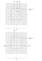
- FIG. 3 is a diagram showing an example of an RGBW pixel arrangement in a general photodetector.
- FIG. 4 is an enlarged view showing a part of the RGBW pixel array shown in FIG. 3.
- FIG. 5 is a diagram showing the quantum efficiency (Qe) of each W pixel in an RGBW pixel array of a general photodetector.
- Qe quantum efficiency
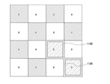
- FIG. 6 is a partial plan view illustrating an example of the color scheme of the outer color filter in the RGBW pixel array in the photodetector according to an embodiment of the present technology.
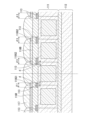
- FIG. 7 is a partial cross-sectional view for explaining the schematic structure of a pixel in the RGBW pixel array shown in FIG. 6 taken along the line VII-VII'.
- FIG. 8 is a partial plan view for explaining another example of the color scheme of the outer peripheral color filter in the RGBW pixel array in the photodetection device according to the embodiment of the present technology.
- FIG. 9 is a partial plan view for explaining still another example of the color arrangement of the outer peripheral color filter in the RGBW pixel array in the photodetection device according to the embodiment of the present technology.
- FIG. 7 is a partial cross-sectional view for explaining the schematic structure of a pixel in the RGBW pixel array shown in FIG. 6 taken along the line VII-VII'.
- FIG. 8 is a partial plan view for explaining another example of the color
- FIG. 10 is a partial plan view for explaining still another example of the color arrangement of the outer peripheral color filter in the RGBW pixel array in the photodetection device according to the embodiment of the present technology.
- FIG. 11 is a diagram for explaining an example of a method for forming a color filter in a manufacturing process of a photodetecting device according to an embodiment of the present technology.
- FIG. 12 is a partial cross-sectional view showing a schematic structure of a pixel in a photodetection device according to an embodiment of the present technology.
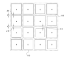
- FIG. 13 is a partial plan view for explaining a shielding film of a pixel in the RGBW pixel array shown in FIG. 12.
- the second semiconductor substrate 12 is a substrate on which various semiconductor integrated circuits 14 are formed.
- the semiconductor integrated circuit 14 includes, for example, a PLL circuit that generates a clock, a pixel control circuit that controls the operation of each pixel P, and a drive that drives a specific pixel P to read out an electrical signal under the control of the pixel control circuit. It includes a circuit, a signal processing circuit for processing read electrical signals, an interface circuit for enabling connection with the outside, and the like. These circuits may be integrally configured as a system-on-chip (SoC) such as a CMOS LSI, for example.
- SoC system-on-chip
- FIG. 2 is a partial cross-sectional view showing a schematic structure of a pixel P in the photodetecting device 1 according to an embodiment of the present technology. That is, the figure shows a part of the cross-sectional structure of a main part of a semiconductor substrate (LSI chip) in which a first semiconductor substrate 11 and a second semiconductor substrate 12 are bonded. In the figure, a dashed line indicated by the symbol B indicates a bonding surface between the first semiconductor substrate 11 and the second semiconductor substrate 12.
- the photodetection device 1 is assumed to be a back-illuminated CMOS image sensor, but is not limited thereto, and may be, for example, a front-illuminated CMOS image sensor.
- the first semiconductor substrate 11 includes a silicon single crystal Si semiconductor layer 111, and a wiring layer 112 laminated on the front surface (the bottom surface in the figure) of the Si semiconductor layer 111. It consists of:
- the Si semiconductor layer 111 includes a semiconductor region 1111 that constitutes a light receiving element.
- the semiconductor region 1111 is a region in which various semiconductor elements such as photodiodes and transistors are formed, and is covered with, for example, a silicon oxide film 1112.
- the wiring layer 112 is formed including various wiring patterns 1121.
- a semiconductor element within the semiconductor region 1111 is electrically connected to the wiring pattern 1121 via a via.
- the wiring layer 112 may typically be configured by stacking a plurality of wiring layers with an interlayer insulating film interposed therebetween.
- the wiring pattern 1121 is formed of, for example, a metal material such as aluminum (Al) or copper (Cu), but is not limited thereto.
- a color filter 116 is formed, for example, via a flattening film 115, and an on-chip lens 117 is further formed thereon.
- the color filter 116 is made of an organic material to which a predetermined coloring material (RGBW) is added, for example, for each pixel P, and is formed by using, for example, photolithography/etching technology.
- RGBW predetermined coloring material
- the color filter 116W of the W pixel may be formed of the transparent material of the on-chip lens 117, for example.
- a part of the on-chip lens 117 formed directly on the flattening film 115 is considered to be the color filter 116W.
- the W pixel, R pixel, G pixel, and B pixel correspond to the first pixel, the second pixel, the third pixel, and the fourth pixel in the claims, respectively.
- the on-chip lens 117 is an optical lens configured to effectively focus or image light incident from the outside onto the pixel P (that is, the photoelectric conversion element of the semiconductor region 1111).
- the on-chip lens 117 is formed so that incident light is coupled to each pixel P.
- the on-chip lens 117 may be configured to be shared by a plurality of adjacent pixels P forming a pixel block. In other words, one on-chip lens 117 may be provided for each pixel block.
- a pixel block corresponds to a pixel unit that indicates the resolution of an image to be reproduced.
- FIG. 3 is a diagram showing an example of an RGBW pixel arrangement in a general photodetector. More specifically, FIG. 3(a) shows an example of an RGBW pixel array in which W pixels are arranged based on the Bayer array, and FIG. 3(b) shows an example of an RGBW pixel array in which W pixels are arranged based on the quad Bayer array. An example of a pixel array is shown. Note that the outer peripheral color filter 118 is not shown in this figure for convenience.
- RGBW pixel arrangement there are three arrangement patterns of pixels of colors other than W adjacent to the W pixel.
- a second array pattern in which the pixel P adjacent to pixel P (W2) (second W pixel) is two G pixels, one R pixel, and one B pixel, and the pixel P (W3) A third arrangement pattern in which the pixels P adjacent to (the third W pixel) are two G pixels and two B pixels.
- the arrangement pattern is such that the pixel P adjacent to the pixel P(W1') (first W pixel) is two G pixels and two R pixels.
- a certain first array pattern a second array pattern in which pixels adjacent to pixel P (W2') (second W pixel) are two G pixels, one R pixel, and one B pixel;
- P(W3') (third W pixel) has a third arrangement pattern in which the pixels adjacent to each other are two G pixels and two B pixels.
- the quantum efficiency Qe of W pixels P(W5) and P(W7) which have a high ratio of adjacent G pixels and B pixels
- the quantum efficiency Qe is the highest at about 88.9%
- the quantum efficiency Qe of the W pixels P(W2) and P(W4) which have a high ratio of adjacent R pixels and G pixels, is the lowest at about 86.8%.
- the quantum efficiency Qe of the W pixels P(W1), P(W3), P(W6), and P(W8) is about 87.8%, which is a value between them.
- the photodetecting device 1 of the present disclosure is configured to use the outer peripheral color filter 118 to eliminate the output level difference between the W pixels in such an RGBW four-color pixel array.
- the first W pixel in the RGBW pixel array i.e., the W pixel surrounded by G pixels x 2 and R pixels x 2
- the second W pixel i.e., G pixels x 2 and R pixels W pixel surrounded by ⁇ 1 and B pixel ⁇ 1
- the output level difference between the second W pixel and the third W pixel i.e., the W pixel surrounded by G pixel ⁇ 2 and B pixel ⁇ 2
- FIG. 9 is a partial plan view for explaining still another example of the color scheme of the outer peripheral color filter in the RGBW pixel array in the photodetection device 1 according to an embodiment of the present technology.
- a blue outer circumferential color filter 118B is formed around the R pixel. Therefore, the arrangement period of the color filters 116 around the W pixel is unified into green x 2 and blue x 2. This makes it possible to eliminate the output level difference between the W pixels.
- the outer periphery color filter 118B corresponds to a fourth outer periphery color filter in the claims.
- FIG. 10 is a partial plan view for explaining still another example of the color arrangement of the outer peripheral color filter in the RGBW pixel arrangement in the photodetection device 1 according to an embodiment of the present technology.
- the outer circumferential color filter 118 shown in the figure is different from that shown in FIG. 6 in that the outer circumferential color filter 118 is not formed in the portion C where the pixels P intersect at their corners. That is, the outer peripheral color filter 118 surrounding the pixel P does not necessarily have to be formed continuously, and may be partially missing (or discontinuous).
- the outer peripheral color filter 118 is formed so as to avoid the intersection C of the corner of the pixel P to ensure the effective area area of the W pixel. Thereby, it is possible to suppress the occurrence of an output level difference between the W pixels, and at the same time, it is possible to suppress the decrease in sensitivity of the W pixels.
- the outer color filter 118G2 has a narrower width than the outer color filter 118G1, so it has less influence on the effective area area of the W pixel. Therefore, the outer color filter 118G1 may not be formed only at the intersection of the corners of R pixels.
- FIG. 11 is a diagram for explaining an example of a method for forming a color filter in a manufacturing process of a photodetecting device according to an embodiment of the present technology.
- the upper diagram is a schematic plan view of the photodetector 1 in the manufacturing process
- the lower diagram is a schematic partial sectional view of the corresponding cut plane. It is.
- the back surface of the deposited Si semiconductor layer 111 is ground, and then a planarization film 115 is formed (FIG. 1(a)).Although not shown, the back surface of the Si semiconductor layer 111 is , a light shielding film 113 is formed.
- RGB color filters 116 are formed.
- the color filters 116 are formed in the order of GRB.
- the W pixel is formed using the material of the on-chip lens 117, for example.
- a green color filter material is formed on the planarization film 115, and is further exposed to light through a photomask pattern and then etched. As a result, a green color filter 116G is formed, and an outer color filter 116G1 around the R pixel and an outer color filter 116G2 around the B pixel are simultaneously formed (FIG. 4(b)).
- a red color filter material is formed on the planarization film 115, and is further exposed to light through a photomask pattern and then etched, thereby forming a red color filter 116R (see (c) in the same figure). )).
- a red color filter material is formed on the planarization film 115, further exposed to light through a photomask pattern, and then etched, thereby forming a red color filter 116B (see (d) in the same figure). ).However, in FIG. 2(d), the cut plane is shifted by one pixel in order to explain the G pixel.).
- the transparent material of the on-chip lens 117 is formed thereon.
- the amount of this transparent material is adjusted so that the portion corresponding to the W pixel is satisfactorily filled.
- the transparent material is reflowed to form a lens curved surface, thereby forming an array of on-chip lenses 117 (FIG. 4(e)).
- the outer circumferential color filter 118 can be formed at the same time as the color filter 116 of the same color using the follo mask pattern. Therefore, since no additional manufacturing process or equipment is required for forming the outer peripheral color filter 118, it is possible to eliminate the above-mentioned output level difference between the W pixels while avoiding an increase in manufacturing costs.
- the outer peripheral color filter 118 by forming the outer peripheral color filter 118, the entry of light in a specific wavelength band from the pixel P adjacent to the W pixel to the W pixel is effectively suppressed or adjusted. Therefore, the output level difference between the W pixels can be eliminated or ignored, so that it is possible to obtain good image quality without appearing as a periodic brightness level difference in the reproduced image.
- the width of the outer color filter 118 is set according to the color of the color filter 116 of the pixel P, it is possible to more effectively suppress the entry of light in a specific wavelength band from the adjacent pixel P to the W pixel. Or you can adjust it.
- This embodiment is a modification of the first embodiment, and is characterized in that the width of the light shielding film 113 formed on the Si semiconductor layer 111 is defined in accordance with the wavelength characteristics of each RGB color filter 116.
- the light shielding film 113 surrounding each RGB pixel P has a first width ⁇ 1 that is the narrowest, and a first width ⁇ 1 that surrounds the G pixel.
- the width of the light shielding film 113 is formed so that it has a second width ⁇ 2 that is thicker than the first width ⁇ 1, and the width of the light shielding film 113 surrounding the B pixel is set to a third width ⁇ 3 that is wider than the second width ⁇ 2. (i.e., ⁇ 1 ⁇ 2 ⁇ 3).
- the narrower the width of the light-shielding film 113 surrounding the pixel P the wider the aperture defined thereby, which can reduce the influence of diffraction.
- the width portion of the light shielding film 113 that defines the aperture of the W pixel may be symmetrical about the boundary of the pixel P. That is, the width d of the portion extending inward from the boundary line between the W pixel and the adjacent pixel P to define the aperture of the W pixel is the same.
- This embodiment is a modification of the first or second embodiment described above, and is characterized in that an outer peripheral color filter 118 is applied to an RGBW pixel array in which W pixels are arranged based on a quad Bayer array.
- An RGBW pixel array in which W pixels are arranged based on a quad Bayer array is a block pixel constructed by arranging a collection of four pixels P in a Bayer array (see Fig. 3(b)). Each set of W pixels contains one W pixel. Even in such an RGBW pixel arrangement, the amount of light that enters the W pixel from the adjacent pixel P relative to the amount of light that directly enters the W pixel differs for each of the three arrangement patterns, and the electrical signal extracted from the W pixel There will be a difference in the output level itself. Therefore, by forming an outer peripheral color filter 118 around the color filter 116, the output step difference between the W pixels is suppressed.
- FIG. 14 is a partial plan view for explaining an example of the color scheme of the outer peripheral color filter in the RGBW pixel array in the photodetector 1 according to an embodiment of the present technology.
- outer peripheral color filters 118G1 and 118G2 are formed for each of the R pixel and the B pixel. Therefore, the arrangement period of the color filters around each W pixel is unified to green.
- the width of the outer color filter 118G1 around the R pixel is wider than the width of the outer color filter 118G2 around the B pixel.
- the outer color filter 118G1 is formed on all three R pixels, but the formation of the outer color filter 118G1 is omitted for the R pixel adjacent to the G pixel (i.e., the upper left R pixel). It's okay to be.
- FIG. 15 is a partial plan view for explaining another example of the color arrangement of the outer peripheral color filter in the RGBW pixel array in the photodetection device 1 according to an embodiment of the present technology.
- the color scheme of the outer peripheral color filter 118 of this example is configured such that a red outer peripheral color filter 118R is formed around the B pixel. Therefore, the arrangement period of the color filters around the W pixel is unified into green x 2 and red x 2. This makes it possible to eliminate the output level difference between the W pixels.
- FIG. 16 is a partial plan view for explaining still another example of the color arrangement of the outer peripheral color filter in the RGBW pixel array in the photodetection device 1 according to an embodiment of the present technology.
- a blue outer circumferential color filter 118R is formed around an R pixel. Therefore, the arrangement period of the color filters around the W pixel is unified to green x 2 and blue x 2. This makes it possible to eliminate the output level difference between the W pixels.
- the technology according to the present disclosure (this technology) can be applied to various products.
- the technology according to the present disclosure may be realized as a device mounted on any type of moving body such as a car, electric vehicle, hybrid electric vehicle, motorcycle, bicycle, personal mobility, airplane, drone, ship, robot, etc. It's okay.
- the drive system control unit 12010 controls the operation of devices related to the drive system of the vehicle according to various programs.
- the drive system control unit 12010 includes a drive force generation device such as an internal combustion engine or a drive motor that generates drive force for the vehicle, a drive force transmission mechanism that transmits the drive force to wheels, and a drive force transmission mechanism that controls the steering angle of the vehicle. It functions as a control device for a steering mechanism to adjust and a braking device to generate braking force for the vehicle.
- the body system control unit 12020 controls the operations of various devices installed in the vehicle body according to various programs.
- the body system control unit 12020 functions as a keyless entry system, a smart key system, a power window device, or a control device for various lamps such as a headlamp, a back lamp, a brake lamp, a turn signal, or a fog lamp.
- radio waves transmitted from a portable device that replaces a key or signals from various switches may be input to the body control unit 12020.
- the body system control unit 12020 receives input of these radio waves or signals, and controls the door lock device, power window device, lamp, etc. of the vehicle.
- the imaging unit 12031 is an optical sensor that receives light and outputs an electrical signal according to the amount of received light.
- the imaging unit 12031 can output the electrical signal as an image or as distance measurement information.
- the light received by the imaging unit 12031 may be visible light or non-visible light such as infrared rays.
- the microcomputer 12051 calculates control target values for the driving force generation device, steering mechanism, or braking device based on the information inside and outside the vehicle acquired by the vehicle exterior information detection unit 12030 or the vehicle interior information detection unit 12040, Control commands can be output to 12010.
- the microcomputer 12051 realizes ADAS (Advanced Driver Assistance System) functions, including vehicle collision avoidance or impact mitigation, following distance based on vehicle distance, vehicle speed maintenance, vehicle collision warning, vehicle lane departure warning, etc. It is possible to perform cooperative control for the purpose of ADAS (Advanced Driver Assistance System) functions, including vehicle collision avoidance or impact mitigation, following distance based on vehicle distance, vehicle speed maintenance, vehicle collision warning, vehicle lane departure warning, etc. It is possible to perform cooperative control for the purpose of
- ADAS Advanced Driver Assistance System
- the microcomputer 12051 controls the driving force generating device, steering mechanism, braking device, etc. based on information about the surroundings of the vehicle acquired by the vehicle exterior information detection unit 12030 or the vehicle interior information detection unit 12040. It is possible to perform cooperative control for the purpose of autonomous driving, etc., which does not rely on operation.
- the microcomputer 12051 can output a control command to the body system control unit 12030 based on the information outside the vehicle acquired by the outside information detection unit 12030.
- the microcomputer 12051 controls the headlamps according to the position of the preceding vehicle or oncoming vehicle detected by the vehicle exterior information detection unit 12030, and performs cooperative control for the purpose of preventing glare, such as switching from high beam to low beam. It can be carried out.
- the audio and image output unit 12052 transmits an output signal of at least one of audio and images to an output device that can visually or audibly notify information to the occupants of the vehicle or to the outside of the vehicle.
- an audio speaker 12061, a display section 12062, and an instrument panel 12063 are illustrated as output devices.
- the display unit 12062 may include, for example, at least one of an on-board display and a head-up display.
- FIG. 18 is a diagram showing an example of the installation position of the imaging section 12031.
- the imaging unit 12031 includes imaging units 12101, 12102, 12103, 12104, and 12105.
- the imaging units 12101, 12102, 12103, 12104, and 12105 are provided at, for example, the front nose of the vehicle 12100, the side mirrors, the rear bumper, the back door, and the upper part of the windshield inside the vehicle.
- An imaging unit 12101 provided in the front nose and an imaging unit 12105 provided above the windshield inside the vehicle mainly acquire images in front of the vehicle 12100.
- Imaging units 12102 and 12103 provided in the side mirrors mainly capture images of the sides of the vehicle 12100.
- An imaging unit 12104 provided in the rear bumper or back door mainly captures images of the rear of the vehicle 12100.
- the imaging unit 12105 provided above the windshield inside the vehicle is mainly used to detect preceding vehicles, pedestrians, obstacles, traffic lights, traffic signs, lanes, and the like.
- FIG. 18 shows an example of the imaging range of the imaging units 12101 to 12104.
- An imaging range 12111 indicates the imaging range of the imaging unit 12101 provided on the front nose
- imaging ranges 12112 and 12113 indicate imaging ranges of the imaging units 12102 and 12103 provided on the side mirrors, respectively
- an imaging range 12114 shows the imaging range of the imaging unit 12101 provided on the front nose.
- the imaging range of the imaging unit 12104 provided in the rear bumper or back door is shown. For example, by overlapping the image data captured by the imaging units 12101 to 12104, an overhead image of the vehicle 12100 viewed from above can be obtained.
- At least one of the imaging units 12101 to 12104 may have a function of acquiring distance information.
- at least one of the imaging units 12101 to 12104 may be a stereo camera including a plurality of image sensors, or may be an image sensor having pixels for phase difference detection.
- the microcomputer 12051 determines the distance to each three-dimensional object within the imaging ranges 12111 to 12114 and the temporal change in this distance (relative speed with respect to the vehicle 12100) based on the distance information obtained from the imaging units 12101 to 12104. By determining the following, it is possible to extract, in particular, the closest three-dimensional object on the path of vehicle 12100, which is traveling at a predetermined speed (for example, 0 km/h or more) in approximately the same direction as vehicle 12100, as the preceding vehicle. can. Furthermore, the microcomputer 12051 can set an inter-vehicle distance to be secured in advance in front of the preceding vehicle, and perform automatic brake control (including follow-up stop control), automatic acceleration control (including follow-up start control), and the like. In this way, it is possible to perform cooperative control for the purpose of autonomous driving, etc., in which the vehicle travels autonomously without depending on the driver's operation.
- automatic brake control including follow-up stop control
- automatic acceleration control including follow-up start control
- At least one of the imaging units 12101 to 12104 may be an infrared camera that detects infrared rays.
- the microcomputer 12051 can recognize a pedestrian by determining whether the pedestrian is present in the images captured by the imaging units 12101 to 12104.
- pedestrian recognition involves, for example, a procedure for extracting feature points in images captured by the imaging units 12101 to 12104 as infrared cameras, and a pattern matching process is performed on a series of feature points indicating the outline of an object to determine whether it is a pedestrian or not.
- the audio image output unit 12052 creates a rectangular outline for emphasis on the recognized pedestrian.
- the display unit 12062 is controlled to display the .
- the audio image output unit 12052 may control the display unit 12062 to display an icon or the like indicating a pedestrian at a desired position.
- the technology according to the present disclosure can be applied to, for example, the imaging unit 12031 among the configurations described above.
- the photodetection device 1 shown in FIG. 1 can be applied to the imaging section 12031.
- steps, acts, or functions may be performed in parallel or in a different order unless the results are inconsistent.
- the steps, acts, and functions described are provided as examples only, and some of the steps, acts, and functions may be omitted or combined with each other without departing from the spirit of the technology. It is also possible to add other steps, actions, or functions.
- a photodetection device comprising a pixel array section in which a plurality of pixels are arranged in an array, Each of the plurality of pixels is a photoelectric conversion element capable of generating an electrical signal according to the received light; a color filter that is formed according to a predetermined color filter pattern on a light-receiving surface of the photoelectric conversion element that receives the light and that transmits light in a specific wavelength band of the light; a first pixel including a first color filter that transmits light in a first wavelength band; a second pixel that is adjacent to the first pixel and includes a second color filter that transmits light in a second wavelength band; a third pixel that is adjacent to the first pixel and includes a third color filter that transmits light in a third wavelength band whose peak wavelength is shorter than the peak wavelength of the second wavelength band; a fourth pixel that is adjacent to the first pixel and includes a fourth color filter that transmits light in a fourth wavelength band
- the fourth pixel includes a second peripheral color filter that is formed to surround the second color filter and that transmits light in the third wavelength band.
- the width of the first outer peripheral color filter is wider than the width of the second outer peripheral color filter.
- the first outer peripheral color filter is formed so as to avoid a portion where the corners of the second pixels intersect,
- the second outer peripheral color filter is formed so as to avoid a portion where the corners of the fourth pixel intersect.
- Each of the plurality of pixels has a light shielding film formed between the light receiving surface of the photoelectric conversion element and the color filter and defining a light receiving area of the photoelectric conversion element.
- the photodetection device according to any one of (1) to (3) above.
- the width of the light shielding film is defined according to the specific wavelength of the light transmitted through the color filter formed in the pixel.
- the light receiving area defined by the light blocking film of the second pixel is wider than the light receiving area defined by the light blocking film of the fourth pixel.
- a photodetection device comprising a pixel array section in which a plurality of pixels are arranged in an array, Each of the plurality of pixels is a photoelectric conversion element capable of generating an electrical signal according to the received light; a color filter that is formed according to a predetermined color filter pattern on a light-receiving surface of the photoelectric conversion element that receives the light and that transmits light in a specific wavelength band of the light; a first pixel including a first color filter that transmits light in a first wavelength band; a second pixel that is adjacent to the first pixel and includes a second color filter that transmits light in a second wavelength band; a third pixel that is adjacent to the first pixel and includes a third color filter that transmits light in a third wavelength band whose peak wavelength is shorter than the peak wavelength of the second wavelength band; a fourth pixel that is adjacent to the first pixel and includes a fourth color filter that transmits light in a fourth wavelength band whose peak wavelength is shorter than the
- the arrangement of the plurality of pixels is an RGBW pixel arrangement in which the first pixels are arranged based on a Bayer arrangement.
- the array of the plurality of pixels is an RGBW pixel array in which the first pixels are arranged based on a Quad Bayer array.
Landscapes
- Engineering & Computer Science (AREA)
- Multimedia (AREA)
- Signal Processing (AREA)
- Physics & Mathematics (AREA)
- Spectroscopy & Molecular Physics (AREA)
- Solid State Image Pick-Up Elements (AREA)
Abstract
Description
1.第1の実施形態
2.第2の実施形態
3.第3の実施形態
4.移動体への応用例
5.まとめ
図1は、本技術の一実施形態に係る光検出装置の概略的構造の一例を説明するための分解斜視図である。同図に示すように、光検出装置1は、第1半導体基板11と、第2半導体基板12とが積層されたLSIチップである。第1半導体基板11と第2半導体基板12とは、例えばフリップチップ実装により接合される。光検出装置1は、後述するように、様々な製品へ適用することができ、画像を撮影する撮像部として機能し得る。
上述した例は、R画素及びB画素の周囲に緑色の外周カラーフィルタ118Gを形成したカラーフィルタの配色構成を示したが、これに限られず、W画素の出力段差の抑制のため、画素Pの色との関係で外周カラーフィルタ118の種々の配色構成を採用することができる。
本実施形態は、第1の実施形態の変形であり、Si半導体層111上に形成される遮光膜113の幅をRGBの各カラーフィルタ116の波長特性に合わせて規定したことを特徴としている。
本実施形態は、第1又は第2の上記実施形態の変形であり、クアッドベイヤー配列をベースにW画素を配列したRGBW画素配列に外周カラーフィルタ118を適用したことを特徴としている。
図15は、本技術の一実施形態に係る光検出装置1におけるRGBW画素配列における外周カラーフィルタの配色構成の他の例を説明するための部分平面図である。同図に示すように、本例の外周カラーフィルタ118の配色構成は、B画素の周囲に赤色の外周カラーフィルタ118Rが形成されて構成される。したがって、W画素の周囲のカラーフィルタの配列周期は、緑色×2と赤色×2に統一される。これにより、W画素間の出力段差を解消することができる。
本開示に係る技術(本技術)は、様々な製品へ応用することができる。例えば、本開示に係る技術は、自動車、電気自動車、ハイブリッド電気自動車、自動二輪車、自転車、パーソナルモビリティ、飛行機、ドローン、船舶、ロボット等のいずれかの種類の移動体に搭載される装置として実現されてもよい。
上記各実施形態は、本技術を説明するための例示であり、本技術をこれらの実施形態にのみ限定する趣旨ではない。本技術は、その要旨を逸脱しない限り、さまざまな形態で実施することができる。
(1)
複数の画素がアレイ状に配列された画素アレイ部を備える光検出装置であって、
前記複数の画素のそれぞれは、
受光した光に応じた電気信号を生成可能な光電変換素子と、
前記光を受光する前記光電変換素子の受光面上に所定のカラーフィルタパターンに従って形成された、前記光のうちの特定の波長帯の光を透過するカラーフィルタと、を備え
前記複数の画素は、
第1の波長帯の光を透過する第1のカラーフィルタを備えた第1の画素と、
前記第1の画素に隣接して第2の波長帯の光を透過する第2のカラーフィルタを備える第2の画素と、
前記第1の画素に隣接して前記第2の波長帯のピーク波長よりも短いピーク波長の第3の波長帯の光を透過する第3のカラーフィルタを備える第3の画素と、
前記第1の画素に隣接して前記第3の波長帯のピーク波長よりも短いピーク波長の第4の波長帯の光を透過する第4のカラーフィルタを備える第4の画素と、を含み、
前記第2の画素は、前記第2のカラーフィルタの周囲を囲むように形成された前記第3の波長帯の光を透過する第1の外周カラーフィルタを含む、
光検出装置。
(2)
前記第4の画素は、前記第2のカラーフィルタの周囲を囲むように形成された前記第3の波長帯の光を透過する第2の外周カラーフィルタを含む、
前記(1)に記載の光検出装置。
(3)
前記受光面に平行な面において、前記第1の外周カラーフィルタの幅は、前記第2の外周カラーフィルタの幅よりも広い、
前記(2)に記載の光検出装置。
(4)
前記第1の外周カラーフィルタは、前記第2の画素のコーナーどうしが交差する部分を避けるように形成され、
前記第2の外周カラーフィルタは、前記第4の画素のコーナーどうしが交差する部分を避けるように形成される、
前記(2)又は(3)に記載の光検出装置。
(5)
前記複数の画素のそれぞれは、前記光電変換素子の受光面と前記カラーフィルタとの間に形成され前記光電変換素子の受光領域を画定する遮光膜を有する、
前記(1)から(3)のいずれか一つに記載の光検出装置。
(6)
前記遮光膜の幅は、前記画素に形成される前記カラーフィルタが透過する前記光の前記特定の波長に応じて規定される、
前記(5)に記載の光検出装置。
(7)
前記第2の画素の前記遮光膜により画定される前記受光領域は、前記第4の画素の前記遮光膜により画定される前記受光領域よりも広い、
前記(6)に記載の光検出装置。
(8)
複数の画素がアレイ状に配列された画素アレイ部を備える光検出装置であって、
前記複数の画素のそれぞれは、
受光した光に応じた電気信号を生成可能な光電変換素子と、
前記光を受光する前記光電変換素子の受光面上に所定のカラーフィルタパターンに従って形成された、前記光のうちの特定の波長帯の光を透過するカラーフィルタと、を備え、
前記複数の画素は、
第1の波長帯の光を透過する第1のカラーフィルタを備えた第1の画素と、
前記第1の画素に隣接して第2の波長帯の光を透過する第2のカラーフィルタを備える第2の画素と、
前記第1の画素に隣接して前記第2の波長帯のピーク波長よりも短いピーク波長の第3の波長帯の光を透過する第3のカラーフィルタを備える第3の画素と、
前記第1の画素に隣接して前記第3の波長帯のピーク波長よりも短いピーク波長の第4の波長帯の光を透過する第4のカラーフィルタを備える第4の画素と、を含み、
前記第4の画素は、前記第2のカラーフィルタの周囲を囲むように形成された前記第2の波長帯の光を透過する第3の外周カラーフィルタを含む、
光検出装置。
(9)
複数の画素がアレイ状に配列された画素アレイ部を備える光検出装置であって、
前記複数の画素のそれぞれは、
受光した光に応じた電気信号を生成可能な光電変換素子と、
前記光を受光する前記光電変換素子の受光面上に所定のカラーフィルタパターンに従って形成された、前記光のうちの特定の波長帯の光を透過するカラーフィルタと、を備え
前記複数の画素は、
第1の波長帯の光を透過する第1のカラーフィルタを備えた第1の画素と、
前記第1の画素に隣接して第2の波長帯の光を透過する第2のカラーフィルタを備える第2の画素と、
前記第1の画素に隣接して前記第2の波長帯のピーク波長よりも短いピーク波長の第3の波長帯の光を透過する第3のカラーフィルタを備える第3の画素と、
前記第1の画素に隣接して前記第3の波長帯のピーク波長よりも短いピーク波長の第4の波長帯の光を透過する第4のカラーフィルタを備える第4の画素と、を含み、
前記第2の画素は、前記第2のカラーフィルタの周囲を囲むように形成された前記第2の波長帯の光を透過する第4の外周カラーフィルタを含む、
光検出装置。
(10)
前記複数の画素の配列は、ベイヤー配列をベースに前記第1の画素を配列したRGBW画素配列である、
前記(1)から(9)のいずれか一つに記載の光検出装置。
(11)
前記複数の画素の配列は、クアッドベイヤー配列をベースに前記第1の画素を配列したRGBW画素配列である、
前記(1)から(9)のいずれか一つに記載の光検出装置。
11…第1半導体基板
111…Si半導体層
1111…半導体領域
1112…シリコン酸化膜
112…配線層
113…遮光膜
114…画素分離部
115…平坦化膜
116…カラーフィルタ
117…オンチップレンズ
118…外周カラーフィルタ
12…第2半導体基板12
121…Si半導体層
122…配線層
13…画素アレイ部
P…画素
Claims (11)
- 複数の画素がアレイ状に配列された画素アレイ部を備える光検出装置であって、
前記複数の画素のそれぞれは、
受光した光に応じた電気信号を生成可能な光電変換素子と、
前記光を受光する前記光電変換素子の受光面上に所定のカラーフィルタパターンに従って形成された、前記光のうちの特定の波長帯の光を透過するカラーフィルタと、を備え
前記複数の画素は、
第1の波長帯の光を透過する第1のカラーフィルタを備えた第1の画素と、
前記第1の画素に隣接して第2の波長帯の光を透過する第2のカラーフィルタを備える第2の画素と、
前記第1の画素に隣接して前記第2の波長帯のピーク波長よりも短いピーク波長の第3の波長帯の光を透過する第3のカラーフィルタを備える第3の画素と、
前記第1の画素に隣接して前記第3の波長帯のピーク波長よりも短いピーク波長の第4の波長帯の光を透過する第4のカラーフィルタを備える第4の画素と、を含み、
前記第2の画素は、前記第2のカラーフィルタの周囲を囲むように形成された前記第3の波長帯の光を透過する第1の外周カラーフィルタを含む、
光検出装置。 - 前記第4の画素は、前記第2のカラーフィルタの周囲を囲むように形成された前記第3の波長帯の光を透過する第2の外周カラーフィルタを含む、
請求項1に記載の光検出装置。 - 前記受光面に平行な面において、前記第1の外周カラーフィルタの幅は、前記第2の外周カラーフィルタの幅よりも広い、
請求項2に記載の光検出装置。 - 前記第1の外周カラーフィルタは、前記第2の画素のコーナーどうしが交差する部分を避けるように形成され、
前記第2の外周カラーフィルタは、前記第4の画素のコーナーどうしが交差する部分を避けるように形成される、
請求項2に記載の光検出装置。 - 前記複数の画素のそれぞれは、前記光電変換素子の受光面と前記カラーフィルタとの間に形成され前記光電変換素子の受光領域を画定する遮光膜を有する、
請求項3に記載の光検出装置。 - 前記遮光膜の幅は、前記画素に形成される前記カラーフィルタが透過する前記光の前記特定の波長に応じて規定される、
請求項5に記載の光検出装置。 - 前記第2の画素の前記遮光膜により画定される前記受光領域は、前記第4の画素の前記遮光膜により画定される前記受光領域よりも広い、
請求項6に記載の光検出装置。 - 複数の画素がアレイ状に配列された画素アレイ部を備える光検出装置であって、
前記複数の画素のそれぞれは、
受光した光に応じた電気信号を生成可能な光電変換素子と、
前記光を受光する前記光電変換素子の受光面上に所定のカラーフィルタパターンに従って形成された、前記光のうちの特定の波長帯の光を透過するカラーフィルタと、を備え、
前記複数の画素は、
第1の波長帯の光を透過する第1のカラーフィルタを備えた第1の画素と、
前記第1の画素に隣接して第2の波長帯の光を透過する第2のカラーフィルタを備える第2の画素と、
前記第1の画素に隣接して前記第2の波長帯のピーク波長よりも短いピーク波長の第3の波長帯の光を透過する第3のカラーフィルタを備える第3の画素と、
前記第1の画素に隣接して前記第3の波長帯のピーク波長よりも短いピーク波長の第4の波長帯の光を透過する第4のカラーフィルタを備える第4の画素と、を含み、
前記第4の画素は、前記第2のカラーフィルタの周囲を囲むように形成された前記第2の波長帯の光を透過する第3の外周カラーフィルタを含む、
光検出装置。 - 複数の画素がアレイ状に配列された画素アレイ部を備える光検出装置であって、
前記複数の画素のそれぞれは、
受光した光に応じた電気信号を生成可能な光電変換素子と、
前記光を受光する前記光電変換素子の受光面上に所定のカラーフィルタパターンに従って形成された、前記光のうちの特定の波長帯の光を透過するカラーフィルタと、を備え
前記複数の画素は、
第1の波長帯の光を透過する第1のカラーフィルタを備えた第1の画素と、
前記第1の画素に隣接して第2の波長帯の光を透過する第2のカラーフィルタを備える第2の画素と、
前記第1の画素に隣接して前記第2の波長帯のピーク波長よりも短いピーク波長の第3の波長帯の光を透過する第3のカラーフィルタを備える第3の画素と、
前記第1の画素に隣接して前記第3の波長帯のピーク波長よりも短いピーク波長の第4の波長帯の光を透過する第4のカラーフィルタを備える第4の画素と、を含み、
前記第2の画素は、前記第2のカラーフィルタの周囲を囲むように形成された前記第2の波長帯の光を透過する第4の外周カラーフィルタを含む、
光検出装置。 - 前記複数の画素の配列は、ベイヤー配列をベースに前記第1の画素を配列したRGBW画素配列である、
請求項1に記載の光検出装置。 - 前記複数の画素の配列は、クアッドベイヤー配列をベースに前記第1の画素を配列したRGBW画素配列である、
請求項1に記載の光検出装置。
Priority Applications (1)
| Application Number | Priority Date | Filing Date | Title |
|---|---|---|---|
| CN202380045467.5A CN119325722A (zh) | 2022-06-15 | 2023-05-02 | 光检测装置 |
Applications Claiming Priority (2)
| Application Number | Priority Date | Filing Date | Title |
|---|---|---|---|
| JP2022096375 | 2022-06-15 | ||
| JP2022-096375 | 2022-06-15 |
Publications (1)
| Publication Number | Publication Date |
|---|---|
| WO2023243252A1 true WO2023243252A1 (ja) | 2023-12-21 |
Family
ID=89190998
Family Applications (1)
| Application Number | Title | Priority Date | Filing Date |
|---|---|---|---|
| PCT/JP2023/017179 Ceased WO2023243252A1 (ja) | 2022-06-15 | 2023-05-02 | 光検出装置 |
Country Status (2)
| Country | Link |
|---|---|
| CN (1) | CN119325722A (ja) |
| WO (1) | WO2023243252A1 (ja) |
Cited By (1)
| Publication number | Priority date | Publication date | Assignee | Title |
|---|---|---|---|---|
| US12154493B1 (en) * | 2023-09-20 | 2024-11-26 | PlayNitride Display Co., Ltd. | Micro light-emitting diode display device |
Citations (3)
| Publication number | Priority date | Publication date | Assignee | Title |
|---|---|---|---|---|
| WO2013121742A1 (ja) * | 2012-02-13 | 2013-08-22 | 富士フイルム株式会社 | 撮像素子 |
| JP2018133575A (ja) * | 2018-03-08 | 2018-08-23 | ソニー株式会社 | 固体撮像装置、電子機器、及び、固体撮像装置の製造方法 |
| JP2020150267A (ja) * | 2020-05-21 | 2020-09-17 | ソニー株式会社 | 固体撮像装置、電子機器、及び、固体撮像装置の製造方法 |
-
2023
- 2023-05-02 CN CN202380045467.5A patent/CN119325722A/zh not_active Withdrawn
- 2023-05-02 WO PCT/JP2023/017179 patent/WO2023243252A1/ja not_active Ceased
Patent Citations (3)
| Publication number | Priority date | Publication date | Assignee | Title |
|---|---|---|---|---|
| WO2013121742A1 (ja) * | 2012-02-13 | 2013-08-22 | 富士フイルム株式会社 | 撮像素子 |
| JP2018133575A (ja) * | 2018-03-08 | 2018-08-23 | ソニー株式会社 | 固体撮像装置、電子機器、及び、固体撮像装置の製造方法 |
| JP2020150267A (ja) * | 2020-05-21 | 2020-09-17 | ソニー株式会社 | 固体撮像装置、電子機器、及び、固体撮像装置の製造方法 |
Cited By (1)
| Publication number | Priority date | Publication date | Assignee | Title |
|---|---|---|---|---|
| US12154493B1 (en) * | 2023-09-20 | 2024-11-26 | PlayNitride Display Co., Ltd. | Micro light-emitting diode display device |
Also Published As
| Publication number | Publication date |
|---|---|
| CN119325722A (zh) | 2025-01-17 |
Similar Documents
| Publication | Publication Date | Title |
|---|---|---|
| US12550465B2 (en) | Imaging element and imaging apparatus | |
| US20240145507A1 (en) | Imaging device | |
| US11928848B2 (en) | Light receiving device, solid-state imaging apparatus, electronic equipment, and information processing system | |
| US20240339469A1 (en) | Optical detector and electronic apparatus | |
| WO2023189130A1 (ja) | 光検出装置及び電子機器 | |
| WO2023243252A1 (ja) | 光検出装置 | |
| US20260090122A1 (en) | Imaging device and electronic device | |
| US20250331326A1 (en) | Photodetection device and electronic device | |
| WO2023203919A1 (ja) | 固体撮像装置 | |
| JP7261168B2 (ja) | 固体撮像装置及び電子機器 | |
| WO2023127512A1 (ja) | 撮像装置、電子機器 | |
| WO2023013493A1 (ja) | 撮像装置及び電子機器 | |
| CN116802812A (zh) | 摄像装置 | |
| WO2025109888A1 (ja) | 光検出装置および電子機器 | |
| JP7654571B2 (ja) | 固体撮像装置およびその製造方法 | |
| WO2025191673A1 (ja) | 光検出素子 | |
| WO2025263404A1 (ja) | 光検出装置 | |
| WO2024135127A1 (ja) | 固体撮像装置 | |
| WO2025084019A1 (ja) | 光検出装置 | |
| WO2023181657A1 (ja) | 光検出装置及び電子機器 | |
| WO2026094424A1 (ja) | 半導体パッケージ、半導体チップ、および、半導体パッケージの製造方法 | |
| WO2025057805A1 (ja) | 撮像素子及び撮像装置 | |
| WO2023233873A1 (ja) | 光検出装置及び電子機器 |
Legal Events
| Date | Code | Title | Description |
|---|---|---|---|
| 121 | Ep: the epo has been informed by wipo that ep was designated in this application |
Ref document number: 23823555 Country of ref document: EP Kind code of ref document: A1 |
|
| WWE | Wipo information: entry into national phase |
Ref document number: 202380045467.5 Country of ref document: CN |
|
| NENP | Non-entry into the national phase |
Ref country code: DE |
|
| WWP | Wipo information: published in national office |
Ref document number: 202380045467.5 Country of ref document: CN |
|
| 122 | Ep: pct application non-entry in european phase |
Ref document number: 23823555 Country of ref document: EP Kind code of ref document: A1 |
|
| NENP | Non-entry into the national phase |
Ref country code: JP |