WO2023242898A1 - センサ - Google Patents
センサ Download PDFInfo
- Publication number
- WO2023242898A1 WO2023242898A1 PCT/JP2022/023613 JP2022023613W WO2023242898A1 WO 2023242898 A1 WO2023242898 A1 WO 2023242898A1 JP 2022023613 W JP2022023613 W JP 2022023613W WO 2023242898 A1 WO2023242898 A1 WO 2023242898A1
- Authority
- WO
- WIPO (PCT)
- Prior art keywords
- film
- dielectric member
- electrode
- tactile sensing
- electrodes
- Prior art date
Links
- 239000011232 storage material Substances 0.000 claims abstract description 14
- 238000009825 accumulation Methods 0.000 claims abstract description 8
- 238000003825 pressing Methods 0.000 claims description 18
- 229920002595 Dielectric elastomer Polymers 0.000 claims description 3
- 239000007788 liquid Substances 0.000 claims description 3
- 229920001971 elastomer Polymers 0.000 abstract description 4
- 230000035945 sensitivity Effects 0.000 abstract description 4
- 239000010408 film Substances 0.000 description 188
- 239000000463 material Substances 0.000 description 22
- OKTJSMMVPCPJKN-UHFFFAOYSA-N Carbon Chemical compound [C] OKTJSMMVPCPJKN-UHFFFAOYSA-N 0.000 description 18
- 230000035807 sensation Effects 0.000 description 18
- XLOMVQKBTHCTTD-UHFFFAOYSA-N Zinc monoxide Chemical compound [Zn]=O XLOMVQKBTHCTTD-UHFFFAOYSA-N 0.000 description 12
- 239000002041 carbon nanotube Substances 0.000 description 12
- 229910021393 carbon nanotube Inorganic materials 0.000 description 12
- 239000012621 metal-organic framework Substances 0.000 description 12
- 238000010586 diagram Methods 0.000 description 10
- 229920002379 silicone rubber Polymers 0.000 description 10
- 239000004945 silicone rubber Substances 0.000 description 10
- BASFCYQUMIYNBI-UHFFFAOYSA-N platinum Chemical compound [Pt] BASFCYQUMIYNBI-UHFFFAOYSA-N 0.000 description 9
- ZLMJMSJWJFRBEC-UHFFFAOYSA-N Potassium Chemical compound [K] ZLMJMSJWJFRBEC-UHFFFAOYSA-N 0.000 description 8
- 229910052700 potassium Inorganic materials 0.000 description 8
- 239000011591 potassium Substances 0.000 description 8
- 239000011701 zinc Substances 0.000 description 8
- 239000013207 UiO-66 Substances 0.000 description 7
- 239000011347 resin Substances 0.000 description 7
- 229920005989 resin Polymers 0.000 description 7
- 239000010409 thin film Substances 0.000 description 7
- JRPBQTZRNDNNOP-UHFFFAOYSA-N barium titanate Chemical compound [Ba+2].[Ba+2].[O-][Ti]([O-])([O-])[O-] JRPBQTZRNDNNOP-UHFFFAOYSA-N 0.000 description 6
- 229910002113 barium titanate Inorganic materials 0.000 description 6
- 238000001514 detection method Methods 0.000 description 6
- 239000010931 gold Substances 0.000 description 6
- 229910021389 graphene Inorganic materials 0.000 description 6
- 239000010936 titanium Substances 0.000 description 6
- 239000011787 zinc oxide Substances 0.000 description 6
- 239000013300 Ni 3(2,3,6,7,10,11-hexaiminotriphenylene)2 Substances 0.000 description 5
- 238000009826 distribution Methods 0.000 description 5
- 239000004205 dimethyl polysiloxane Substances 0.000 description 4
- 235000013870 dimethyl polysiloxane Nutrition 0.000 description 4
- 239000012528 membrane Substances 0.000 description 4
- 239000007769 metal material Substances 0.000 description 4
- 229920000435 poly(dimethylsiloxane) Polymers 0.000 description 4
- YCKRFDGAMUMZLT-UHFFFAOYSA-N Fluorine atom Chemical compound [F] YCKRFDGAMUMZLT-UHFFFAOYSA-N 0.000 description 3
- RTAQQCXQSZGOHL-UHFFFAOYSA-N Titanium Chemical compound [Ti] RTAQQCXQSZGOHL-UHFFFAOYSA-N 0.000 description 3
- 229920006311 Urethane elastomer Polymers 0.000 description 3
- 229920000800 acrylic rubber Polymers 0.000 description 3
- 229910052782 aluminium Inorganic materials 0.000 description 3
- XAGFODPZIPBFFR-UHFFFAOYSA-N aluminium Chemical compound [Al] XAGFODPZIPBFFR-UHFFFAOYSA-N 0.000 description 3
- 239000004020 conductor Substances 0.000 description 3
- 238000005516 engineering process Methods 0.000 description 3
- 229910052731 fluorine Inorganic materials 0.000 description 3
- 239000011737 fluorine Substances 0.000 description 3
- 229920001973 fluoroelastomer Polymers 0.000 description 3
- 239000004088 foaming agent Substances 0.000 description 3
- PCHJSUWPFVWCPO-UHFFFAOYSA-N gold Chemical compound [Au] PCHJSUWPFVWCPO-UHFFFAOYSA-N 0.000 description 3
- 229910052737 gold Inorganic materials 0.000 description 3
- 239000012212 insulator Substances 0.000 description 3
- 238000000465 moulding Methods 0.000 description 3
- CXQXSVUQTKDNFP-UHFFFAOYSA-N octamethyltrisiloxane Chemical compound C[Si](C)(C)O[Si](C)(C)O[Si](C)(C)C CXQXSVUQTKDNFP-UHFFFAOYSA-N 0.000 description 3
- 238000004987 plasma desorption mass spectroscopy Methods 0.000 description 3
- 229910052697 platinum Inorganic materials 0.000 description 3
- 229920000058 polyacrylate Polymers 0.000 description 3
- 229920002981 polyvinylidene fluoride Polymers 0.000 description 3
- 229910052719 titanium Inorganic materials 0.000 description 3
- BQCIDUSAKPWEOX-UHFFFAOYSA-N 1,1-Difluoroethene Chemical compound FC(F)=C BQCIDUSAKPWEOX-UHFFFAOYSA-N 0.000 description 2
- 229920001780 ECTFE Polymers 0.000 description 2
- VYPSYNLAJGMNEJ-UHFFFAOYSA-N Silicium dioxide Chemical compound O=[Si]=O VYPSYNLAJGMNEJ-UHFFFAOYSA-N 0.000 description 2
- 238000006243 chemical reaction Methods 0.000 description 2
- 229920000840 ethylene tetrafluoroethylene copolymer Polymers 0.000 description 2
- 239000012530 fluid Substances 0.000 description 2
- 229920002493 poly(chlorotrifluoroethylene) Polymers 0.000 description 2
- 239000005023 polychlorotrifluoroethylene (PCTFE) polymer Substances 0.000 description 2
- 229920001343 polytetrafluoroethylene Polymers 0.000 description 2
- 239000004810 polytetrafluoroethylene Substances 0.000 description 2
- 229940058401 polytetrafluoroethylene Drugs 0.000 description 2
- USOVQUNFIOLNFQ-UHFFFAOYSA-N triphenylene-1,2,3,4,5,6-hexaimine Chemical group N=C1C(C=2C=3C(C(C(C(C3C3=CC=CC=C3C2C=C1)=N)=N)=N)=N)=N USOVQUNFIOLNFQ-UHFFFAOYSA-N 0.000 description 2
- CHJAYYWUZLWNSQ-UHFFFAOYSA-N 1-chloro-1,2,2-trifluoroethene;ethene Chemical group C=C.FC(F)=C(F)Cl CHJAYYWUZLWNSQ-UHFFFAOYSA-N 0.000 description 1
- 238000010146 3D printing Methods 0.000 description 1
- 239000004812 Fluorinated ethylene propylene Substances 0.000 description 1
- -1 MXene Substances 0.000 description 1
- 229920001774 Perfluoroether Polymers 0.000 description 1
- 210000001142 back Anatomy 0.000 description 1
- 239000011324 bead Substances 0.000 description 1
- 238000004891 communication Methods 0.000 description 1
- 238000005520 cutting process Methods 0.000 description 1
- 230000005611 electricity Effects 0.000 description 1
- HQQADJVZYDDRJT-UHFFFAOYSA-N ethene;prop-1-ene Chemical group C=C.CC=C HQQADJVZYDDRJT-UHFFFAOYSA-N 0.000 description 1
- 239000005357 flat glass Substances 0.000 description 1
- 238000003384 imaging method Methods 0.000 description 1
- 230000002452 interceptive effect Effects 0.000 description 1
- 238000003475 lamination Methods 0.000 description 1
- 230000000149 penetrating effect Effects 0.000 description 1
- 229920009441 perflouroethylene propylene Polymers 0.000 description 1
- 229920000642 polymer Polymers 0.000 description 1
- 229920006254 polymer film Polymers 0.000 description 1
- 230000036316 preload Effects 0.000 description 1
- 230000015541 sensory perception of touch Effects 0.000 description 1
- 239000000377 silicon dioxide Substances 0.000 description 1
- 230000003068 static effect Effects 0.000 description 1
- 230000000638 stimulation Effects 0.000 description 1
- 239000000126 substance Substances 0.000 description 1
- 230000002123 temporal effect Effects 0.000 description 1
- 210000000707 wrist Anatomy 0.000 description 1
Images


Classifications
-
- G—PHYSICS
- G01—MEASURING; TESTING
- G01L—MEASURING FORCE, STRESS, TORQUE, WORK, MECHANICAL POWER, MECHANICAL EFFICIENCY, OR FLUID PRESSURE
- G01L1/00—Measuring force or stress, in general
- G01L1/16—Measuring force or stress, in general using properties of piezoelectric devices
-
- G—PHYSICS
- G01—MEASURING; TESTING
- G01L—MEASURING FORCE, STRESS, TORQUE, WORK, MECHANICAL POWER, MECHANICAL EFFICIENCY, OR FLUID PRESSURE
- G01L5/00—Apparatus for, or methods of, measuring force, work, mechanical power, or torque, specially adapted for specific purposes
Definitions
- the present invention relates to sensors, and particularly to sensors that convert applied force, pressure, or vibration into voltage.
- Haptic and force feedback are important for surgical systems and teleoperation tasks.
- haptic and force feedback it is necessary to detect applied force, pressure or vibration.
- Sometani et al. worked to create a system that could measure biological information without interfering with the movement of the living body by attaching it to human tissue or the surface of the body.
- By forming an organic device on an ultra-thin polymer film with a thickness of about 1 micrometer they succeeded in creating a flexible organic device that is extremely thin but surprisingly durable.
- the world's lightest, thinnest, and soft organic transistor integrated circuit that they have created maintains its electrical performance and is mechanically unbreakable even when the film is bent to a radius of curvature of 5 micrometers.
- Someya et al. successfully created a prototype soft touch sensor system using this organic transistor integrated circuit.
- Non-Patent Document 1 Similar sensors are being researched at Stanford University (for example, see Non-Patent Document 1).
- the present invention was made in view of this situation, and aims to make it thinner and more flexible so that force, pressure, or vibration can be detected with higher sensitivity.
- a sensor includes a first film that generates a voltage when force, pressure, or vibration is applied, and a membrane provided on one surface of the first film at a predetermined distance from each other.
- a second film that generates a voltage when force, pressure, or vibration is applied; and a film-like second electrode provided on one surface of the second film. is formed of dielectric rubber into a thin plate shape with holes formed therein, and the other side of the first film is pasted on the first side, which is a predetermined side, so as to face the first side.
- a voltage is generated between any or all of the first electrodes and the second electrode in response to the applied force, pressure, or vibration.
- the spacing between the plurality of first electrodes provided on one surface of the first film can be less than the two-point discrimination threshold of human skin.
- a predetermined voltage can be applied to the dielectric member to precharge the dielectric member.
- a hole formed in the dielectric member can penetrate from the first surface to the second surface.
- One of the plurality of first electrodes and the second electrode may be arranged to sandwich the first film and the second film, and to sandwich the portion of the dielectric member in which the hole is formed. can.
- the cross-sectional shape of the hole formed in the dielectric member on the first surface can be made similar to the shape of the surface of the film-like first electrode.
- the first electrode can be placed on the cross section of the first surface of the hole formed in the dielectric member with the first film in between.
- One of the plurality of first electrodes and the second electrode are sandwiched between the first film and the second film, and the portion of the dielectric member that is outside the portion where the hole is formed is sandwiched between the first and second electrodes. can be placed.
- a pressing means for sandwiching and pressing the first film, the second film, and the ends of the dielectric member can be further provided.
- a plurality of second electrodes can be provided, and each of the plurality of second electrodes can be provided at a position facing each of the plurality of first electrodes.
- a pressing means for displacing and pressing the first film, first electrode, second film, second electrode, and dielectric member against the skin is used. Further, it is possible to provide.
- the pressing means can displace the first film, the first electrode, the second film, the second electrode, and the dielectric member and press them against the skin using gas or liquid pressure.
- the pressing means can use a cam to displace the first film, the first electrode, the second film, the second electrode, and the dielectric member and press them against the skin.
- the first film, first electrode, second film, second electrode, and dielectric member can be displaced and pressed against the skin.
- force, pressure, or vibration can be detected with higher sensitivity by making it thinner and more flexible.
- FIG. 1 is a block diagram of a tactile sensing system 11 including a tactile sensing pad that is an example of a sensor.
- 2 is a diagram showing an example of the configuration of a tactile sensing pad group 21.
- FIG. 7 is a diagram showing another example of the configuration of the tactile sensing pad group 21.
- FIG. 7 is a diagram showing still another example of the configuration of the tactile sensing pad group 21.
- FIG. 7 is a plan view showing an example of the configuration of a tactile sensing pad 73.
- FIG. 6 is a cross-sectional view showing a cross section of the tactile sensing pad 73 taken along line AA′ in FIG. 5.
- FIG. 3 is a cross-sectional view showing a cross section of a tactile sensing pad 251.
- FIG. 3 is a cross-sectional view showing a cross section of a tactile sensing pad 301.
- FIG. 7 is a cross-sectional view showing a cross section of a tactile sensing pad 351.
- FIG. 4 is a cross-sectional view showing a cross section of a tactile sensing pad 401.
- FIG. 7 is a diagram showing a state of a tactile sensing pad 73 attached to a finger pad.
- FIG. 1 is a block diagram of a tactile sensing system 11 including a tactile sensing pad, which is an example of a sensor.
- the tactile sensing system 11 converts force, pressure, or vibration that causes a tactile or pressure sensation to a human into information.
- the tactile sensing system 11 detects the unevenness or pattern of the object and the force of contact with the object when the object is touched with a human finger, palm, or robot hand.
- the object to be touched with a human finger, palm, or robot hand may be anything that has substance, and may be a natural person or an object.
- the tactile sensing system 11 includes a tactile sensing pad group 21, a robot system 22, a tactile/pressure drive information calculation system 41, a virtual reality computer system/remote robot manipulation system 42, and an image processing system 43.
- the tactile sensing pad group 21 includes a plurality of tactile generating pads and an actuator that presses a predetermined tactile generating pad against the skin. Tactile sensing pad group 21 detects force, pressure, or vibration. It can also be said that the tactile sensing pad group 21 detects the tactile sensation of the target.
- the tactile sensing pad group 21 is created using MEMS (Micro Electro Mechanical Systems), ultra-precision cutting, 3D printing technology (three-dimensional modeling technology), and precision lamination technology.
- the tactile sensing pad group 21 is worn on the body, such as the finger, palm, back of the hand, wrist, elbow, shoulder, chest, back, or waist, using a fixing band, harness, gloves, or clothing.
- the shape of the tactile sensing pad group 21 is a surface shape corresponding to the palm side surface of the distal phalanx of the second finger (index finger), and has a thickness of 0.2 mm or more and less than 0.5 mm.
- the shape of the tactile sensing pad group 21 is a surface shape corresponding to the palm side surface of the right hand, and has a thickness of 0.2 mm or more and less than 0.5 mm.
- the tactile sensing pad group 21 is attached to the palm of the hand, when a person touches an object such as a person or an object with the palm, the tactile sensing pad group 21 is pressed against the object such as a person or object. Detect force, pressure or vibration.
- the tactile sensing pad group 21 outputs the detected force, pressure, or vibration as voltage.
- the tactile sensing pad group 21 detects force, pressure, or vibration that causes a tactile sensation, pressure sensation, or vibration sensation, and outputs the detected force, pressure, or vibration as a voltage. In other words, the tactile sensing pad group 21 detects the target's tactile, pressure, or vibrational sensations.
- the robot system 22 is equipped with a robot hand and performs operations such as touching, grasping, and carrying objects such as people and objects.
- a tactile sensing pad group 21 is attached to the robot hand of the robot system 22. Tactile sensing pad group 21 detects force, pressure, or vibration. That is, when the robot hand of the robot system 22 touches or grasps an object such as a person or an object, the tactile sensation of the object is detected as force, pressure, or vibration. For example, the tactile sensing pad group 21 and the robot system 22 trace the surface of the object and detect tactile sensations corresponding to the shape of the object, such as unevenness and patterns.
- the tactile/pressure drive information calculation system 41 acquires force, pressure, or vibration signals that indicate the touch of the target and are detected by the tactile sensing pad group 21 .
- a contact object an object that the tactile sensing pad group 21 touches and detects force, pressure, or vibration, and that is a person or an object, will be referred to as a contact object.
- the image processing system 43 includes an imaging device, an image processing device, and the like, and estimates the unevenness and pattern of the object and the force at the time of contact from an image taken of an object such as a person or an object, and estimates the unevenness and pattern of the object and the force at the time of contact.
- Information indicating the force at the time of contact is supplied to the tactile/pressure drive information calculation system 41.
- the tactile/pressure drive information calculation system 41 is comprised of an analog signal processing device, a computer system, etc., and converts force, pressure, or vibration data that indicates the touch of the object detected by the tactile sensing pad group 21 into information that can be handled by a computer. Convert.
- the tactile/pressure drive information calculation system 41 applies signal processing such as noise removal and dynamic range conversion to force, pressure, or vibration signals that indicate the touch of a contact target, which are acquired from the tactile sensing pad group 21. , performs analog/digital conversion.
- the tactile/pressure drive information calculation system 41 converts force, pressure, or vibration data, which is digital data, into data in a predetermined format.
- the haptic/pressure drive information calculation system 41 converts force, pressure, or vibration data into data in a format in which values indicating force or pressure are arranged to indicate spatial or temporal positions.
- the tactile/pressure drive information calculation system 41 converts information indicating the unevenness and pattern of the object estimated by the image processing system 43, and the force at the time of contact into force, pressure, or vibration data in a predetermined format. do.
- the tactile/pressure drive information calculation system 41 also calculates the unevenness and pattern of the target estimated by the image processing system 43, the force at the time of contact, and the force indicating the feel of the contact target detected by the tactile sensing pad group 21. , pressure or vibration data.
- the tactile/pressure drive information calculation system 41 supplies force, pressure, or vibration data in a predetermined format to the virtual reality computer system/remote robot manipulation system 42 .
- the virtual reality computer system/remote robot manipulation system 42 uses force, pressure, or vibration data in a predetermined format for communication in the metaverse (virtual reality) or for presenting tactile or pressure sensations during work using a remote robot. Used for control. For example, the virtual reality computer system/remote robot manipulation system 42 calculates the avatar's contact, abutment, or collision with other avatars or objects in the virtual space in response to the avatar's movements in the virtual space. For example, the virtual reality computer system/remote robot manipulation system 42 calculates haptic information such as tactile, pressure, or vibration sensations of other avatars or objects when the avatar contacts or collides with other avatars or objects in virtual space. do.
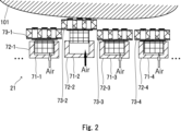
- FIG. 2 is a diagram showing an example of the configuration of the tactile sensing pad group 21.
- the tactile sensing pad group 21 includes approximately three to ten tactile sensing pads 73.
- Each tactile sensing pad 73 has 10 to 50 detection points.
- Detection points on the tactile sensing pad 73 are arranged in the left-right direction in FIG. 2 and in the front-back direction (depth direction) in FIG. That is, the detection points are two-dimensionally arranged on the surface of the tactile sensing pad 73 at predetermined intervals on the side of the surface that contacts the object to be touched.
- the tactile sensing pad group 21 is a predetermined tactile sensing pad 73 among the plurality of tactile sensing pads 73 arranged in a row, and when it comes into contact with a contact target and detects force, pressure, or vibration, the tactile sensing pad group 21 is a predetermined tactile sensing pad 73 of the plurality of tactile sensing pads 73 arranged in a row. A predetermined tactile sensing pad 73 is moved in the direction of the contact target so as to make contact with the tactile sensing pad 73 .
- tactile sensing pad group 21 includes four tactile sensing pads 73, when distinguishing the tactile sensing pads 73 individually, they will be referred to as tactile sensing pads 73-1 to 73-4, etc.
- FIG. 2 shows an example of the configuration of the tactile sensing pad group 21 including four tactile sensing pads 73-1 to 73-4.
- Tactile sensing units 71-1 to 71-4 are configured to include air actuators 72-1 to 72-4, respectively, and tactile sensing pads 73-1 to 73-4, respectively.
- the tactile sensing units 71-1 to 71-4 each operate individually and independently to detect force, pressure, or vibration.
- the tactile sensing pad 73-1 has a plurality of electrodes formed on the surface of the tactile sensing pad 73-1 that is in contact with the contact target 101.
- each of the tactile sensing pads 73-2 to 73-4 has a surface that is in contact with the contact target 101 among the surfaces of each of the tactile sensing pads 73-2 to 73-4, which will be described in detail later.
- a plurality of electrodes are formed.
- a plurality of electrodes formed on the surface in contact with the contact target 101 are detection points for detecting force, pressure, or vibration, respectively.
- the spacing between the plurality of electrodes formed on each of the tactile sensing pads 73-1 to 73-4 is set to be less than the two-point discrimination threshold of human skin. That is, the distance between the electrodes is less than the two-point discrimination threshold of human skin.
- the two-point discrimination threshold for human skin is 1 to 6 mm at the tip of a finger, and 15 to 20 mm at the palm or sole of the foot.
- the two-point discrimination threshold for human skin is 2 to 3 mm for the lips, and 30 mm for the dorsum of the hand or foot.
- the two-point discrimination threshold of human skin is 2 to 3 mm on the lips, which is the shortest on the body.
- the information obtained in -4 can be used on any part of the body.
- the tactile sensing pads 73-1 to 73-4 are moved in the direction of the contact target 101 by the air actuators 72-1 to 72-4, respectively, so as to contact a predetermined portion of the contact target 101.
- Air actuators 72-1 to 72-4 are pneumatic actuators each consisting of a cylinder and a piston. Air actuators 72-1 to 72-4 each have a piston that protrudes from the cylinder when compressed air at a predetermined pressure is supplied, and tactile sensing pads 73-1 to 73-4 fixed to the piston. By displacing either one of them, it is moved in the direction of the contact target 101.
- the tactile sensing pad 73-2 For example, at a predetermined time, compressed air of a predetermined pressure is supplied to the air actuator 72-2, and the tactile sensing pad 73-2 is moved toward the contact target 101 by displacing the tactile sensing pad 73-2. , the air actuator 72-3, and the air actuator 72-4 are not supplied with compressed air at a predetermined pressure, so the tactile sensing pad 73-1, the tactile sensing pad 73-3, and the tactile sensing pad 73-4 are moved toward the contact target 101. Do not move it to At this time, the tactile sensing pad 73-2 detects force, pressure, or vibration. That is, at this time, the tactile sensing pad 73-2 detects the unevenness or pattern of the contact object 101, or the force, pressure, or vibration that comes into contact with the contact object 101.
- all of the tactile sensing pads 73-1 to 73-4 or one or more of the tactile sensing pads 73-1 to 73-4 actuate the air actuators 72-1 to 72-4. Either the tactile sensing pads 73-1 to 73-4 are moved in the direction of the contact target 101 so as to come into contact with a predetermined part of the contact target 101, or all of the tactile sensing pads 73-1 to 73-4 are moved away from the contact target 101. It will be done.
- tactile sensing units 71-1 to 71-4 individually when there is no need to distinguish the tactile sensing units 71-1 to 71-4 individually, they will be simply referred to as tactile sensing units 71.
- air actuators 72-1 to 72-4 individually when there is no need to distinguish the air actuators 72-1 to 72-4 individually, they will be simply referred to as air actuators 72.
- FIG. 3 is a diagram showing another example of the configuration of the tactile sensing pad group 21 including four tactile sensing pads 73-1 to 73-4.
- Tactile sensing units 121-1 to 121-4 each include tactile sensing pads 73-1 to 73-4, cams 122-1 to 122-4, and motors 123-1 to 123-4, respectively. It is configured as follows. Tactile sensing units 121-1 to 121-4 each operate individually and independently to detect force, pressure, or vibration.
- Tactile sensing pads 73-1 to 73-4 in FIG. 3 come into contact with predetermined portions of contact target 101 by cams 122-1 to 122-4 and motors 123-1 to 123-4, respectively. It is moved in the direction of the contact target 101 so that the touch object 101 moves.
- each of the cams 122-1 to 122-4 is a rotary plate cam.
- each of the cams 122-1 to 122-4 is made of an eccentric disc.
- motors 123-1 to 123-4 are each electric motors. That is, the cams 122-1 to 122-4 are rotated by the motors 123-1 to 123-4, respectively, and are placed at predetermined angular positions relative to the tactile sensing pads 73-1 to 73-4, respectively. If this happens, each of the tactile sensing pads 73-1 to 73-4 is pushed toward the contact target 101.
- the tactile sensing pad 73-2 moves toward the tactile sensing pad 73-2.
- -2 is pushed out and displaced to move it in the direction of the contact target 101, and the cams 122-1, 122-3, and 122-4 are connected to the motors 123-1, 123-3, and 123-4, respectively.
- the tactile sensing pad 73-2 detects force, pressure, or vibration. That is, at this time, the tactile sensing pad 73-2 detects the unevenness or pattern of the contact object 101, or the force, pressure, or vibration that comes into contact with the contact object 101.
- all of the tactile sensing pads 73-1 to 73-4 or one or more of the tactile sensing pads 73-1 to 73-4 activate each of the cams 122-1 to 122-4. , either the tactile sensing pads 73-1 to 73-4 are moved in the direction of the contact target 101 so as to come into contact with a predetermined part of the contact target 101, or all of the tactile sensing pads 73-1 to 73-4 are moved away from the contact target 101. .
- the tactile sensing pads 73-1 to 73-4 are urged away from the contact target 101 by a spring or the like (not shown).
- each of the cams 122-1 to 122-4 has been described as a plate cam, the present invention is not limited to this, and may be a grooved cam or a three-dimensional cam.
- the motors 123-1 to 123-4 have been described as being electric motors, they are not limited to this, and may be a pressure motor, a molecular motor, or an ultrasonic motor that utilizes fluid pressure.
- tactile sensing units 121-1 to 121-4 when there is no need to distinguish the tactile sensing units 121-1 to 121-4 individually, they will simply be referred to as tactile sensing units 121.
- cams 122-1 to 122-4 individually when there is no need to distinguish the cams 122-1 to 122-4 individually, they will be simply referred to as cams 122.
- motors 123-1 to 123-4 individually when there is no need to distinguish the motors 123-1 to 123-4 individually, they are simply referred to as motors 123.
- FIG. 4 is a diagram showing still another example of the configuration of the tactile sensing pad group 21 including four tactile sensing pads 73-1 to 73-4.
- the tactile sensing units 151-1 to 151-4 respectively connect the tactile sensing pads 73-1 to 73-4, the wires 152-1 to 152-4, the pulleys 153-1 to 153-4, and the pulleys 153-1 to 153-4 respectively.
- Tactile sensing units 151-1 to 151-4 each operate individually and independently to detect force, pressure, or vibration.
- Tactile sensing pads 73-1 to 73-4 in FIG. 4 correspond to wires 152-1 to 152-4, pulleys 153-1 to 153-4, and pulleys 154-1 to 154-4, respectively. , and motors 155-1 to 155-4, the contact object 101 is moved in the direction of the contact object 101 so as to contact a predetermined portion of the contact object 101.
- One end of each of the wires 152-1 to 152-4 is fixed to each of the tactile sensing pads 73-1 to 73-4, and the other end of each of the wires 152-1 to 152-4 is fixed to one of the pulleys 154-1 to 152-4. 154-4 respectively.
- the pulleys 153-1 to 153-4 are each rotatably supported.
- the wires 152-1 to 152-4 are hung on pulleys 153-1 to 153-4, respectively, and the extending directions of the wires 152-1 to 152-4 are changed.
- Pulleys 154-1 to 154-4 are rotated by motors 155-1 to 155-4, respectively.
- Motors 155-1 to 155-4 are each electric motors.
- the wires 152-1 to 152 wound around each of the pulleys 154-1 to 154-4 are rotated.
- each of the tactile sensing pads 73-1 to 73-4 fixed to one end of each of the wires 152-1 to 152-4 is pulled and displaced.
- the pulleys 154-1 to 154-4 are rotated by the motors 155-1 to 155-4, respectively, and wind up the wires 152-1 to 152-4, respectively, and the tactile sensing pad 73-1
- Each of the wires 152-1 to 152-4 pulls and presses each of the wires 152-1 to 73-4 against the contact target 101.
- pulley 154-2 is rotated by motor 155-2 to take up wire 152-2, causing wire 152-2 to pull and displace tactile sensing pad 73-2.
- the pulleys 154-1, 154-3, and 154-4 are moved toward the contact target 101, and the tactile sensing pad 73 -1, the tactile sensing pad 73-3 and the tactile sensing pad 73-4 are not moved in the direction of the contact target 101;
- the tactile sensing pad 73-2 detects force, pressure, or vibration. That is, at this time, the tactile sensing pad 73-2 detects the unevenness or pattern of the contact object 101, or the force, pressure, or vibration of contact with the contact object 101.
- all of the tactile sensing pads 73-1 to 73-4 or one or more of the tactile sensing pads 73-1 to 73-4 act on each of the pulleys 153-1 to 153-4.
- it is moved in the direction of the contact target 101 so as to contact a predetermined part of the contact target 101.
- all of the tactile sensing pads 73-1 to 73-4 are moved away from the contact target 101.
- the tactile sensing pads 73-1 to 73-4 are urged away from the contact target 101 by a spring or the like (not shown).
- the tactile sensing pad group 21 including the tactile sensing units 151-1 to 151-4 can be realized as a glove-type device.
- motors 155-1 to 155-4 are each described as being an electric motor, they are not limited to this, and may be a pressure motor, a molecular motor, or an ultrasonic motor that utilizes fluid pressure.
- tactile sensing units 151-1 to 151-4 when there is no need to distinguish the tactile sensing units 151-1 to 151-4 individually, they will simply be referred to as tactile sensing units 151.
- wires 152-1 to 152-4 individually when there is no need to distinguish the wires 152-1 to 152-4 individually, they will simply be referred to as wires 152.
- pulleys 153-1 to 153-4 individually when there is no need to distinguish the pulleys 153-1 to 153-4 individually, they are simply referred to as pulleys 153.
- pulleys 154 When it is not necessary to individually distinguish pulleys 154-1 to 154-4, they are simply referred to as pulleys 154.
- motors 155-1 to 155-4 individually when there is no need to distinguish the motors 155-1 to 155-4 individually, they are simply referred to as motors 155.
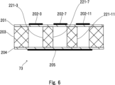
- FIG. 5 is a plan view showing an example of the configuration of the tactile sensing pad 73.
- FIG. 6 is a cross-sectional view showing a cross section of the tactile sensing pad 73 taken along line AA' in FIG.
- the tactile sensing pad 73 includes a film 201, electrodes 202-1 to 202-12, a dielectric member 203, a film 204, and an electrode 205.
- the thickness of the tactile sensing pad 73 is 0.2 mm or more and less than 0.5 mm.
- the tactile sensing pad 73 detects force, pressure, or vibration. For example, the tactile sensing pad 73 generates a voltage signal corresponding to the magnitude of force, the distribution of pressure, or the amplitude or period of vibration.
- the electrodes 202-1 to 202-12 are provided on one surface of the film 201. Electrode 205 is provided on one surface of film 204.
- the other surface of the film 201 is attached to a first surface of the dielectric member 203, which is the upper surface in FIG. 6 (hereinafter also simply referred to as the upper surface).
- the other surface of the film 204 is attached to a second surface (the lower surface in FIG. 6 (hereinafter also simply referred to as the lower surface)) opposite to the first surface. ing. That is, the film 201 and the film 204 are bonded together with the dielectric member 203 in between.
- the planar shape of the film 201, the planar shape of the dielectric member 203, and the planar shape of the film 204 are the same.
- the planar shape of the film 201, the dielectric member 203, and the planar shape of the film 204 are rectangular.
- the film 201, the dielectric member 203, and the film 204 are bonded together so that they overlap each other when viewed in a planar direction.
- the electrodes 202-1 to 202-12 are provided on the outer surface of the film 201 that is bonded to the film 204 with the dielectric member 203 sandwiched therebetween.
- the electrode 205 is provided on the outer surface of the film 204 that is bonded to the film 201 with the dielectric member 203 sandwiched therebetween.
- the film 201 is an example of a first film, and is a film formed into a membrane shape from a polymeric material. Film 201 generates a voltage when force, pressure or vibration is applied.
- the film 204 is an example of a second film, and is a film formed into a membrane shape from a polymeric material. Film 204 generates a voltage when force, pressure or vibration is applied.
- the film 201 and the film 204 are respectively piezoelectric films such as PVDF (Poly Vinylidene DiFluoride), FEP (Fluorinated Ethylene Propylene), PTFE (Poly Tetra Fluoro Ethylene), PFA (Per Fluoro Alkoxy polymer), and ETFE (Ethylene Tetra Fluoro Ethylene copolymer).
- Fluorine resin film such as PVDF, PCTFE (Poly Chloro Tri Fluoro Ethylene) or ECTFE (Ethylene Chloro Tri Fluoro Ethylene copolymer).
- the material of the film 204 may be the same as the material of the film 201 or may be different.
- the dielectric member 203 is a dielectric and an insulator, and is made of a flexible material and is formed into a thin plate shape.
- the dielectric member 203 is made of rubber such as silicone rubber, PDMS (dimethylpolysiloxane), fluororubber, acrylic rubber, or urethane rubber.
- the dielectric member 203 includes a hole 221-1 (not shown), a hole 221-2 (not shown), a hole 221-3, a hole 221-4 (not shown) to a hole 221-6 (not shown). , hole 221-7, hole 221-8 (not shown) to hole 221-10 (not shown), hole 221-11, and hole 221-12 (not shown) are formed.
- the holes 221-1 to 221-12 penetrate from the surface of the dielectric member 203 from the surface on the film 201 side to the surface on the film 204 side. That is, the holes 221-1 to 221-12 penetrate from the upper surface to the lower surface of the dielectric member 203.
- the upper surface of the dielectric member 203 is an example of a first surface.
- the lower surface of dielectric member 203 is an example of the second surface.
- the electrodes 202-1 to 202-12 are made of a conductor and formed into a film shape.
- the electrodes 202-1 to 202-12 are a film made of a metal material such as gold (Au), platinum (Pt), titanium (Ti), or aluminum (Al), or a carbon nanotube (CNT) electrode film.
- the electrodes 202-1 to 202-12 are formed to be flexible. Electrodes 202-1 to 202-12 are insulated from each other.
- the electrodes 202-1 to 202-12 are each formed in a circular thin film shape on one surface of the film 201.
- the electrodes 202-1 to 202-12 are each formed in a circular shape with a diameter of 1 mm.
- the electrodes 202-1 to 202-12 are detection points for detecting force, pressure, or vibration, respectively.
- the spacing between the electrodes 202-1 to 202-12 is less than the two-point discrimination threshold of human skin.
- the spacing between the electrodes 202-1 to 202-12 is less than 2 mm.
- the interval between the electrodes 202-1 to 202-12 is the distance from the center to the center of each of the circularly formed electrodes 202-1 to 202-12, or the distance between the circularly formed electrodes 202-1 to 202-12. The distance from each outer edge to the outer edge of 202-12.
- the terminals 212-1 to 212-12 are terminals for outputting the voltage from each of the electrodes 202-1 to 202-12 through the wiring portions 211-1 to 211-12, respectively.
- the terminals 212-1 to 212-12 and the wiring portions 211-1 to 211-12 are molded from the same material as the electrodes 202-1 to 202-12.
- Each of the terminals 212-1 to 212-12 is formed into a circular thin film shape.
- the wiring parts 211-1 to 211-12 are each made of a flat thin film that connects each of the terminals 212-1 to 212-12 and each of the electrodes 202-1 to 202-12, or are connected to each other. It consists of a plurality of flat thin films.
- terminals 212-1, 212-2, 212-5, 212-6, 212-9, and 212-10 are arranged along one side of the film 201 whose top surface is rectangular. It is located. Terminal 212-3 is placed along the side opposite to one side of film 201 on which terminal 212-1, terminal 212-2, terminal 212-5, terminal 212-6, terminal 212-9, and terminal 212-10 are arranged. , terminal 212-4, terminal 212-7, terminal 212-8, terminal 212-11, and terminal 212-12 are arranged. For example, the terminals 212-1 to 212-12 are each electrically connected to the outside by wire bonding.
- a voltage is generated in each of the electrodes 202-1 to 202-12 due to pressure on the tactile sensing pad 73 or deformation of the tactile sensing pad 73.
- the voltages generated at the electrodes 202-1 to 202-12 are transmitted to the terminals 212-1 to 212-12, respectively.
- the electrode 205 is made of a conductor and formed into a film shape.
- the electrode 205 is a film made of a metal material such as gold (Au), platinum (Pt), titanium (Ti), or aluminum (Al), or a carbon nanotube (CNT) electrode film.
- Electrode 205 is formed to be flexible.
- the electrode 205 is formed into a rectangular thin film shape on one surface of the film 204.
- Electrode 205 is formed to face all of electrodes 202-1 to 202-12. That is, the electrode 205 is formed so as to sandwich all of the electrodes 202-1 to 202-12, the film 201, the dielectric member 203, and the film 204. In other words, the electrode 205 is formed to overlap all of the electrodes 202-1 to 202-12 in the thickness direction of the film 201, dielectric member 203, and film 204.
- the hole 221-3 is formed in a columnar shape with a circular cross section so that the upper and lower surfaces of the dielectric member 203 are circular.
- the end of the hole 221-3 on the upper surface of the dielectric member 203 coincides with the outer periphery of the electrode 202-3.
- the electrode 205 covers the end of the hole 221-3 on the lower surface of the dielectric member 203 on one surface of the film 204.
- the hole 221-7 is formed in a columnar shape with a circular cross section so that the upper and lower surfaces of the dielectric member 203 are circular.
- the end of the hole 221-7 on the upper surface of the dielectric member 203 coincides with the outer periphery of the electrode 202-7.
- the electrode 205 covers the end of the hole 221-7 on the lower surface of the dielectric member 203 on one side of the film 204.
- the hole 221-11 is formed in a columnar shape with a circular cross section so that the upper and lower surfaces of the dielectric member 203 are circular.
- the end of the hole 221-11 on the upper surface of the dielectric member 203 coincides with the outer periphery of the electrode 202-11.
- the electrode 205 covers the end of the hole 221-11 on the lower surface of the dielectric member 203 on one side of the film 204.
- the holes 221-1 and 221-2, the holes 221-4 to 221-6, the holes 221-8 to 221-10, and the hole 221-12 are arranged so that they are circular on the upper and lower surfaces of the dielectric member 203. It is formed into a columnar shape with a circular cross section.
- the ends of the holes 221-1 and 221-2, the holes 221-4 to 221-6, the holes 221-8 to 221-10, and the hole 221-12 on the upper surface of the dielectric member 203 are connected to the electrodes 202-1 and 202, respectively.
- -2 coincides with the respective outer peripheries of the electrodes 202-4 to 202-6, the electrodes 202-8 to 202-10, and the electrode 202-12.
- the electrode 205 is connected to the dielectric member 203 of each of the holes 221-1 and 221-2, the holes 221-4 to 221-6, the holes 221-8 to 221-10, and the hole 221-12 on one surface of the film 204. It covers the edge of the lower surface of.
- one of the electrodes 202-1 to 202-12 and the electrode 205 are formed in either the hole 221-1 or the hole 221-12 in the dielectric member 203 with the film 201 and the film 204 in between. They are arranged so as to sandwich the part that is
- each of the holes 221-1 to 221-12 formed in the dielectric member 203 on the upper surface of the dielectric member 203 is similar to the shape of each surface of the film-like electrodes 202-1 to 202-12. has been done.
- each of the electrodes 202-1 to 202-12 is a cross section of each of the holes 221-1 to 221-12 formed in the dielectric member 203 with the film 201 in between, and placed on the cross section.
- the tactile sensing pad 73 is precharged by applying a voltage of 100V to 15KV.
- a voltage is applied as a precharge between the electrodes 202-1 to 202-12 and the electrode 205, charges are accumulated between the film 201 and the film 204, especially in the holes 221-1 to 221-12 of the dielectric member 203. be done. Precharging the charge causes the tactile sensing pad 73 to generate a larger voltage with less force, pressure, or vibration.
- the applied force or pressure is generated between all or any of the electrodes 202-1 to 202-12 and the electrode 205. Or generate voltage according to vibration.
- the magnitude of the force increases between all or any of the electrodes 202-1 to 202-12 and the electrode 205. , generates a voltage depending on the magnitude of pressure or the amplitude of vibration.
- the tactile sensing pad 73 is mainly made of resin or silicone rubber, it can be easily deformed, fits the contact object 101, and absorbs force, pressure, or vibration caused by the movement of the contact object 101, or force or pressure applied to the contact object 101. Or vibration can be detected.
- the tactile sensing pad 73 can generate a larger voltage with smaller force, pressure, or vibration. will begin to occur.
- the holes 221-1 to 221-12 penetrate from the top surface to the bottom surface of the dielectric member 203, they do not penetrate from the top surface to the bottom surface of the dielectric member 203, but are hollow from the top or bottom surface of the dielectric member 203.
- the hole may have a hollow shape, or may be a bubble-like hole inside the dielectric member 203.
- the electrodes 202-1 to 202-12 are each formed in a circular thin film shape on one surface of the film 201, the electrodes 202-1 to 202-12 are each formed in a polygonal shape such as an ellipse, an oblong, a triangle, or a square. It may be.
- force, pressure, or vibration applied to all or any part of the electrodes 202-1 to 202-12 can be detected.
- electrodes 202-1 to 202-12 individually when there is no need to distinguish the electrodes 202-1 to 202-12 individually, they will simply be referred to as electrodes 202.
- holes 221-1 to 221-12 individually when there is no need to distinguish the holes 221-1 to 221-12 individually, they will be simply referred to as holes 221.
- the materials for forming the dielectric member 203 include graphene, carbon nanotubes, barium titanate, potassium, zinc oxide, MXene, Zn 2 TTFTB and Cd 2 TTBFT, and Ni 3 (2,3,6,7,10,11-
- a charge storage agent such as MOF (Metal Organic Frameworks) materials such as hexaiminotriphenylene) 2 [Ni 3 (HITP) 2 ], Zr-UiO-66, and ZIF-67
- MOF Metal Organic Frameworks
- a charge storage agent such as graphene, carbon nanotubes, barium titanate, potassium, zinc oxide, MXene, or MOF material can be inserted into the hole 221 to assist charge accumulation.
- MXene Zn 2 TTFTB and Cd 2 TTBFT, Ni 3 (2,3,6,7,10,11-hexaiminotriphenylene) 2 [Ni 3 (HITP) 2 ], Zr-UiO-66, ZIF-67, etc.
- a charge storage agent such as a MOF material is mixed into the dielectric member 203 or inserted into the hole 221, the tactile sensing pad 73 can be used without being charged with electric charge in advance.
- the holes 221 can be formed in the dielectric member 203 by mixing 0.1% to 5% by weight of a foaming agent to create air bubbles inside.
- Human skin has many receptors for sensing vibration, shape, and shear forces.
- the tactile sensing pad 73 comes into contact with the contact object 101 and detects force, pressure, or vibration, it generates a voltage corresponding to the force, pressure, or vibration that activates receptors in the human skin, that is, a voltage corresponding to the tactile and pressure sensations. It is possible to generate a corresponding voltage.
- the tactile sensing pad 73 is capable of detecting force, pressure or vibrations on the touch object 101 that activate receptors in the human skin. It can also be said that the tactile sensing pad 73 is capable of detecting force, pressure, or vibration that generates tactile and pressure sensations.
- a device that applies a stimulus that causes a tactile, pressure, or vibration sensation can be used to It can reproduce tactile, pressure or vibration sensations applied to the skin.
- the tactile sensing pad 73 is pressed against the contact target 101 by the air actuator 72, the cam 122 and the motor 123, or the wire 152, the pulley 153, the pulley 154 and the motor 155.
- force, pressure, or vibration is applied to all or any part of the electrodes 202-1 to 202-12 in the state, the tactile sensing pad 73 A voltage is generated between either of them and the electrode 205 depending on the magnitude of force, the magnitude of pressure, or the amplitude of vibration.
- FIG. 7 is a cross-sectional view showing a cross section of the tactile sensing pad 251. As shown in FIG. 7, the same parts as those shown in FIG. 6 are designated by the same reference numerals, and the explanation thereof will be omitted.
- the tactile sensing pad 251 detects force, pressure, or vibration. For example, the tactile sensing pad 251 generates a voltage signal corresponding to the magnitude of force, the distribution of pressure, or the amplitude or period of vibration.
- the tactile sensing pad 251 includes a film 201, electrodes 202-1 to 202-12, a film 204, an electrode 205, and a dielectric member 261.
- the thickness of the tactile sensing pad 251 is 0.2 mm or more and less than 0.5 mm.
- the other surface of the film 201 is attached to the first surface of the dielectric member 261, which is the upper surface in FIG. 7 (hereinafter also simply referred to as the upper surface).
- the other surface of the film 201 is attached to the second surface (the lower surface in FIG. 7 (hereinafter also simply referred to as the lower surface)) opposite to the first surface. ing. That is, the film 201 and the film 204 are bonded together with the dielectric member 261 in between.
- the planar shape of the film 201, the planar shape of the dielectric member 261, and the planar shape of the film 204 are the same.
- planar shape of the film 201, the planar shape of the dielectric member 261, and the planar shape of the film 204 are rectangular.
- the film 201, the dielectric member 261, and the film 204 are bonded together so that they overlap each other when viewed in a planar direction.
- the dielectric member 261 is a dielectric and an insulator, and is made of a flexible material and is formed into a thin plate shape.
- the dielectric member 261 is made of rubber such as silicone rubber, PDMS, fluororubber, acrylic rubber, or urethane rubber.
- Holes 271-1 to 271-9 are formed in the dielectric member 261. The holes 271-1 to 271-9 penetrate from the upper surface to the lower surface of the dielectric member 261. Note that although FIG.
- FIG. 7 shows the cross sections of the electrode 202-3, the electrode 202-7, and the electrode 202-11, the electrode 202-1, the electrode 202-5, the electrode 202-9, the electrode 202-2, Holes 271-1 to 271-9 are also formed in the portions of the dielectric member 261 between the electrode 202-6 and the electrode 202-10, and between the electrode 205 and the electrode 202-4, the electrode 202-8, and the electrode 202-12, respectively. A similar hole is formed.
- the electrode 205 is formed to overlap all of the electrodes 202-1 to 202-12 in the thickness direction of the film 201, dielectric member 261, and film 204.
- the holes 271-1 to 271-9 are each formed in a columnar shape with a circular cross section so that the upper and lower surfaces of the dielectric member 261 are circular.
- the diameter of the bottom surface of each of the holes 271-1 to 271-9 is smaller than the diameter of each of the electrodes 202-3, 202-7, and 202-11.
- Electrode 202-3 is arranged on one surface of film 201 to cover hole 271-2 and hole 271-3.
- Electrode 202-7 is arranged on one surface of film 201 so as to cover hole 271-5.
- Electrode 202-11 is arranged on one surface of film 201 so as to cover hole 271-7 and hole 271-8.
- each of the electrodes 202-3, 202-7, and 202-11 is arranged on one surface of the film 201 so as to cover one or two of the holes 271-1 to 271-9. It is located in The electrode 205 covers the ends of the holes 271-1 to 271-9 on the lower surface of the dielectric member 261 on one surface of the film 204.
- holes 271-1, 271-4, 271-6, and 271-9 are removed from the portion of the dielectric member 261 that is sandwiched between the electrodes 202-1 to 202-12 and the electrode 205. It is formed in the part where the
- each of the electrodes 202-3, 202-7, and 202-11 is arranged to cover any one or two of the holes 271-1 to 271-9. That is, the electrodes 202-3, 202-7, and 202-11 are connected to the holes 271-2, 271-3, 271-5, and 271- formed in the dielectric member 261 through the film 201. 7 and holes 271-8 are disposed on the cross section of the upper surface of the dielectric member 261.
- the tactile sensing pad 251 is precharged with a voltage of 100V to 15KV.
- a voltage is applied as a precharge between the electrodes 202-1 to 202-12 and the electrode 205, the gap between the film 201 and the film 204, especially the holes 271-1 to 221-9 of the dielectric member 261 and the hole 271- Charges are accumulated in holes similar to 1 to 271-9.
- Precharging the charge causes the tactile sensing pad 251 to generate a larger voltage with less force, pressure, or vibration.
- the force, pressure, or vibration When force, pressure, or vibration is applied to a predetermined portion or the entire tactile sensing pad 251, the force, pressure, or vibration is generated between all or any of the electrodes 202-1 to 202-12 and the electrode 205. Generates the appropriate voltage. For example, when force, pressure, or vibration is applied to a predetermined portion or the entire tactile sensing pad 251, the magnitude of the force increases between all or any of the electrodes 202-1 to 202-12 and the electrode 205. , generates a voltage depending on the magnitude of pressure or the amplitude of vibration.
- the tactile sensing pad 251 is mainly made of resin or silicone rubber, it can be easily deformed, fits the contact object 101, and absorbs force, pressure, or vibration caused by the movement of the contact object 101, or force or pressure applied to the contact object 101. Or vibration can be detected.
- the tactile sensing pad 251 When the ratio of the area of the holes 271-1 to 271-9 and holes similar to the holes 271-1 to 271-9 to the entire area of the dielectric member 261 is 10% to 40%, the tactile sensing pad 251 is , a smaller force, pressure or vibration will generate a larger voltage.
- the holes 271-1 to 271-9 and the holes similar to the holes 271-1 to 271-9 penetrate from the upper surface to the lower surface of the dielectric member 261, but they do not penetrate from the upper surface to the lower surface of the dielectric member 261.
- the hole may be recessed from the upper or lower surface of the dielectric member 261 without penetrating it, or may be a bubble-like hole inside the dielectric member 261.
- holes 271-1 to 271-9 will be simply referred to as holes 271 when there is no need to distinguish them individually.
- the materials for forming the dielectric member 261 include graphene, carbon nanotubes, barium titanate, potassium, zinc oxide, MXene, Zn 2 TTFTB and Cd 2 TTBFT, and Ni 3 (2,3,6,7,10,11-
- a charge storage agent such as MOF (Metal Organic Frameworks) materials such as hexaiminotriphenylene) 2 [Ni 3 (HITP) 2 ], Zr-UiO-66, and ZIF-67, dielectric Accumulation of charge in member 261 can be assisted.
- MOF Metal Organic Frameworks
- a charge storage agent such as 0.5% to 50% by volume of graphene, carbon nanotubes, barium titanate, potassium, zinc oxide, MXene, or MOF material may be placed in the hole 271 to assist charge accumulation. .
- MXene Zn 2 TTFTB and Cd 2 TTBFT, Ni 3 (2,3,6,7,10,11-hexaiminotriphenylene) 2 [Ni 3 (HITP) 2 ], Zr-UiO-66, ZIF-67, etc.
- a charge storage agent such as a MOF material is mixed into the dielectric member 261 or inserted into the hole 271, the tactile sensing pad 251 can be used without being charged with electric charge in advance.
- the holes 271 can be formed in the dielectric member 261 by mixing 0.1% to 5% by weight of a foaming agent to create air bubbles inside.
- FIG. 8 is a cross-sectional view showing a cross section of the tactile sensing pad 301. As shown in FIG. In FIG. 8, the same parts as those shown in FIG. 6 are designated by the same reference numerals, and the explanation thereof will be omitted.
- the tactile sensing pad 301 detects force, pressure, or vibration. For example, the tactile sensing pad 301 generates a voltage signal corresponding to the magnitude of force, the distribution of pressure, or the amplitude or period of vibration.
- the tactile sensing pad 301 includes a film 201, electrodes 202-1 to 202-12, a film 204, an electrode 205, and a dielectric member 311.
- the thickness of the tactile sensing pad 301 is 0.2 mm or more and less than 0.5 mm.
- the other surface of the film 201 is attached to the first surface of the dielectric member 311, which is the upper surface in FIG. 8 (hereinafter also simply referred to as the upper surface).
- the other surface of the film 201 is attached to the second surface (the lower surface in FIG. 8 (hereinafter also simply referred to as the lower surface)) opposite to the first surface. ing. That is, the film 201 and the film 204 are bonded together with the dielectric member 311 in between.
- the planar shape of the film 201, the planar shape of the dielectric member 311, and the planar shape of the film 204 are the same.
- planar shape of the film 201, the dielectric member 311, and the planar shape of the film 204 are rectangular.
- the film 201, the dielectric member 311, and the film 204 are bonded together so that they overlap each other when viewed in a planar direction.
- the dielectric member 311 is a dielectric and an insulator, and is made of a flexible material and is formed into a thin plate shape.
- the dielectric member 311 is made of rubber such as silicone rubber, PDMS, fluororubber, acrylic rubber, or urethane rubber.
- Holes 321-1 to 321-4 are formed in the dielectric member 311. The holes 321-1 to 321-4 penetrate from the upper surface to the lower surface of the dielectric member 311. Note that although FIG.
- FIG. 8 shows the cross sections of the electrode 202-3, the electrode 202-7, and the electrode 202-11, the electrode 202-1, the electrode 202-5, the electrode 202-9, the electrode 202-2, Holes 321-1 to 321-4 are also formed in the portions of the dielectric member 311 between the electrode 202-6, the electrode 202-10, and the electrode 205, respectively, and the electrode 202-4, the electrode 202-8, and the electrode 202-12. A similar hole is formed.
- the electrode 205 is formed to overlap all of the electrodes 202-1 to 202-12 in the thickness direction of the film 201, dielectric member 311, and film 204.
- the holes 321-1 to 321-4 are each formed in a columnar shape with a circular cross section so that the upper and lower surfaces of the dielectric member 311 are circular.
- the hole 321-1 is formed between the left end side of the dielectric member 311 in FIG. 8 and the portion sandwiched between the electrode 202-3 and the electrode 205.
- the hole 321-2 is formed between a portion sandwiched between the electrode 202-3 and the electrode 205 and a portion sandwiched between the electrode 202-7 and the electrode 205.
- the hole 321-3 is formed between a portion sandwiched between the electrode 202-7 and the electrode 205 and a portion sandwiched between the electrode 202-11 and the electrode 205.
- the hole 321-4 is formed between the portion sandwiched by the electrode 202-7 and the electrode 205 and the right end side of the dielectric member 311 in FIG.
- each of the electrodes 202-3, 202-7, and 202-11 and the electrode 205 are removed from the portion of the dielectric member 311 where the holes 321-1 to 321-4 are formed. They are arranged to sandwich the parts. In other words, each of the electrodes 202-3, 202-7, and 202-11 and the electrode 205 sandwich the portion of the dielectric member 311 where the holes 321-1 to 321-4 are not formed. It is located.
- the holes 321-1 to 321-4 are formed in a portion of the dielectric member 311 that is outside the portion sandwiched between the electrodes 202-1 to 202-12 and the electrode 205.
- the tactile sensing pad 301 is precharged with a voltage of 100V to 15KV.
- a voltage is applied as a precharge between the electrodes 202-1 to 202-12 and the electrode 205, the gap between the film 201 and the film 204, especially the holes 321-1 to 321-4 of the dielectric member 311 and the hole 321- Charges are accumulated in holes similar to those 1 to 321-4. Precharging the charge causes the tactile sensing pad 301 to generate a larger voltage with less force, pressure, or vibration.
- the force, pressure, or vibration When force, pressure, or vibration is applied to a predetermined portion or the entire tactile sensing pad 301, the force, pressure, or vibration is generated between all or any of the electrodes 202-1 to 202-12 and the electrode 205. Generates the appropriate voltage. For example, when force, pressure, or vibration is applied to a predetermined portion or the entire tactile sensing pad 301, the magnitude of the force increases between all or any of the electrodes 202-1 to 202-12 and the electrode 205. , generates a voltage depending on the magnitude of pressure or the amplitude of vibration.
- the tactile sensing pad 301 is mainly made of resin or silicone rubber, it can be easily deformed, fits the contact object 101, and absorbs force, pressure, or vibration caused by the movement of the contact object 101, or force or pressure applied to the contact object 101. Or vibration can be detected.
- the tactile sensing pad 301 When the ratio of the area of the holes 321-1 to 321-4 and holes similar to the holes 321-1 to 321-4 to the entire area of the dielectric member 311 is 10% to 40%, the tactile sensing pad 301 , a smaller force, pressure or vibration will generate a larger voltage.
- the holes 321-1 to 321-4 and the holes similar to the holes 321-1 to 321-4 penetrate from the top surface to the bottom surface of the dielectric member 311, they penetrate from the top surface to the bottom surface of the dielectric member 311.
- the hole may not penetrate through the hole, but may be recessed from the top or bottom surface of the dielectric member 311, or may be a bubble-like hole inside the dielectric member 311.
- holes 321-1 to 321-4 will be simply referred to as holes 321 when there is no need to distinguish them individually.
- the materials for forming the dielectric member 311 include graphene, carbon nanotubes, barium titanate, potassium, zinc oxide, MXene, Zn 2 TTFTB and Cd 2 TTBFT, and Ni 3 (2,3,6,7,10,11- A dielectric _ Accumulation of charge in the member 311 can be assisted.
- a charge storage agent such as 0.5% to 50% by volume of graphene, carbon nanotubes, barium titanate, potassium, zinc oxide, MXene, or MOF material may be placed in the hole 321 to assist in charge accumulation. .
- MXene Zn 2 TTFTB and Cd 2 TTBFT, Ni 3 (2,3,6,7,10,11-hexaiminotriphenylene) 2 [Ni 3 (HITP) 2 ], Zr-UiO-66, ZIF-67, etc.
- a charge storage agent such as a MOF material is mixed into the dielectric member 311 or inserted into the hole 321, the tactile sensing pad 301 can be used without being charged with electric charge in advance.
- the holes 321 can be formed in the dielectric member 311 by mixing 0.1% to 5% by weight of a foaming agent to create air bubbles inside.
- FIG. 9 is a cross-sectional view showing a cross section of the tactile sensing pad 351. As shown in FIG. 9, parts similar to those shown in FIG. 6 are designated by the same reference numerals, and their explanations will be omitted.
- the tactile sensing pad 351 detects force, pressure, or vibration. For example, the tactile sensing pad 351 generates a voltage signal corresponding to the magnitude of force, the distribution of pressure, or the amplitude or period of vibration.
- the tactile sensing pad 351 includes a film 201, electrodes 202-1 to 202-12, a dielectric member 203, a film 204, and electrodes 361-1 to 361-12.
- the thickness of the tactile sensing pad 351 is 0.2 mm or more and less than 0.5 mm.
- FIG. 9 shows the cross sections of the electrodes 202-3, 202-7, and 202-11, as well as the electrodes 361-3, 361-7, and 361-7, the electrodes 202-1 and A hole 321-1 is formed in the part of the dielectric member 311 between the electrode 361-1 (not shown), and a hole 321-1 is formed in the part of the dielectric member 311 between the electrode 202-2 and the electrode 361-2 (not shown).
- a hole 321-2 is formed in the portion, and similarly, each of the electrodes 202-4 to 202-6 and each of the electrodes 361-4 (not shown) to 361-6 (not shown) are connected to each other.
- Holes 321-4 to 321-4 are formed in the dielectric member 311 between each of the electrodes 202-8 to 202-10 and the electrodes 361-8 (not shown) to 361-10 ( Holes 321-8 to 321-10 are formed in the portions of the dielectric member 311 between the electrodes 202-12 and 361-12 (not shown), respectively.
- a hole 321-12 is formed in the dielectric member 311.
- Each of the electrodes 361-1 to 361-12 is made of a conductor and formed into a film shape.
- each of the electrodes 361-1 to 361-12 is a film made of a metal material such as gold (Au), platinum (Pt), titanium (Ti), or aluminum (Al), or a carbon nanotube (CNT) electrode film.
- the electrodes 361-1 to 361-12 are formed to be flexible. Electrodes 361-1 to 361-12 are insulated from each other.
- the electrodes 361-1 to 361-12 are each formed in a circular thin film shape on one surface of the film 204.
- the electrodes 361-1 to 361-12 are each formed in a circular shape with a diameter of 1 mm.
- Each of the electrodes 361-1 to 361-12 is provided with a wiring portion and a terminal, similarly to each of the electrodes 202-1 to 202-12.
- Each of the electrodes 361-1 to 361-12 is formed to face each of the electrodes 202-1 to 202-12. Each of the electrodes 361-1 to 361-12 is formed to sandwich the film 201, dielectric member 203, and film 204 between each of the electrodes 202-1 to 202-12. Electrode 361-1 is placed at a position facing electrode 202-1 with film 201, dielectric member 203, and film 204 in between. Electrode 361-2 is placed at a position facing electrode 202-2 with film 201, dielectric member 203, and film 204 in between. Similarly, each of the electrodes 361-3 to 361-12 is formed at a position facing each of the electrodes 202-3 to 202-12 with the film 201, dielectric member 203, and film 204 in between.
- each of the electrodes 361-1 to 361-12 is formed at a position facing each of the electrodes 202-1 to 202-12 in the thickness direction of the film 201, dielectric member 203, and film 204.
- the end of the hole 221-3 on the lower surface of the dielectric member 203 coincides with the outer periphery of the electrode 361-3.
- the electrode 361-3 covers the end of the hole 221-3 on the lower surface of the dielectric member 203 on one surface of the film 204.
- the end of the hole 221-7 on the lower surface of the dielectric member 203 coincides with the outer periphery of the electrode 361-7.
- the electrode 361-7 covers the end of the hole 221-7 on the lower surface of the dielectric member 203 on one side of the film 204.
- the end of the hole 221-11 on the lower surface of the dielectric member 203 coincides with the outer periphery of the electrode 361-11.
- the electrode 361-11 covers the end of the hole 221-11 on the lower surface of the dielectric member 203 on one side of the film 204.
- the ends of the holes 221-1 and 221-2, the holes 221-4 to 221-6, the holes 221-8 to 221-10, and the hole 221-12 on the lower surface of the dielectric member 203 are connected to the electrodes 361-1 and 361, respectively.
- -2 coincides with the outer periphery of each of the electrodes 361-4 to 361-6, the electrodes 361-8 to 361-10, and the electrode 361-12.
- Each of the electrodes 361-1 and 361-2, the electrodes 361-4 to 361-6, the electrodes 361-8 to 361-10, and the electrode 361-12 is provided through holes 221-1 and 221 on one surface of the film 204.
- holes 221-4 to 221-6, holes 221-8 to 221-10, and hole 221-12 covering the ends of the lower surface of the dielectric member 203, respectively.
- each of the electrodes 202-1 to 202-12 and each of the electrodes 361-1 to 361-12 are connected to the hole 221-1 and the hole in the dielectric member 203 with the film 201 and the film 204 in between. 221-12 are arranged so as to sandwich the formed portions thereof.
- the tactile sensing pad 351 is precharged with a voltage of 100V to 15KV.
- a voltage is applied as a precharge between the electrodes 202-1 to 202-12 and the electrodes 361-1 to 361-12, the holes 221-1 to 221 in the dielectric member 203 are Charge is accumulated at -12. Precharging the charge causes the tactile sensing pad 351 to generate a larger voltage with less force, pressure, or vibration.
- the tactile sensing pad 351 When force, pressure, or vibration is applied to a predetermined portion or the entirety of the tactile sensing pad 351, the tactile sensing pad 351 is activated between the electrode 202-1 and the electrode 361-1 or between the electrode 202-12 and the electrode 361-12. Either generates a voltage in response to force, pressure or vibration. For example, when force, pressure, or vibration is applied to a predetermined portion or the entirety of the tactile sensing pad 351, the tactile sensing pad 351 detects a gap between the electrode 202-1 and the electrode 361-1 or between the electrode 202-12 and the electrode 361-12. A voltage is generated in all or any of them depending on the magnitude of the force, the magnitude of the pressure, or the amplitude of the vibration.
- the tactile sensing pad 351 is mainly made of resin or silicone rubber, it can be easily deformed, fits the contact object 101, and absorbs force, pressure, or vibration caused by the movement of the contact object 101, or force or pressure applied to the contact object 101. Or vibration can be detected.
- the tactile sensing pad 351 can generate a larger voltage with smaller force, pressure, or vibration. will begin to occur.
- electrodes 361-1 to 361-12 individually, they will be simply referred to as electrodes 361.
- MXene Zn 2 TTFTB and Cd 2 TTBFT, Ni 3 (2,3,6,7,10,11-hexaiminotriphenylene) 2 [Ni 3 (HITP) 2 ], Zr-UiO-66, ZIF-67, etc.
- a charge storage agent such as a MOF material is mixed into the dielectric member 203 or inserted into the hole 221, the tactile sensing pad 351 can be used without being charged with electric charge in advance.
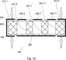
- FIG. 10 is a cross-sectional view showing a cross section of the tactile sensing pad 401. As shown in FIG. In FIG. 10, parts similar to those shown in FIG. 6 are designated by the same reference numerals, and their explanations will be omitted.
- Tactile sensing pad 401 detects force, pressure, or vibration.
- the tactile sensing pad 401 generates a voltage signal corresponding to the magnitude of force, the distribution of pressure, or the amplitude or period of vibration.
- the tactile sensing pad 401 includes a film 201, electrodes 202-1 to 202-12, a dielectric member 203, a film 204, an electrode 205, and springs 411-1 and 411-2.
- the thickness of the tactile sensation generating pad 411 is 0.2 mm or more and less than 0.5 mm.
- the springs 411-1 and 411-2 are made of a spring material and have a U-shaped cross section.
- the spring 411-1 pinches and presses the left ends of the film 201, dielectric member 203, and film 204 in FIG. 10 with a force of 10 mN to 0.5N.
- the spring 411-2 pinches and presses the right end portions of the film 201, the dielectric member 203, and the film 204 in FIG.
- the springs 411-1 and 411-2 sandwich and press the ends of the film 201, dielectric member 203, and film 204. In this way, a larger voltage can be generated with smaller force, pressure, or vibration.
- the spring 411-1 and the spring 411-2 can be molded from a metal material or resin. Further, although it has been described that the spring 411-1 and the spring 411-2 sandwich the opposite ends of the film 201, the dielectric member 203, and the film 204, the present invention is not limited to this. It is possible to adopt a configuration that allows pressing with.
- the tactile sensing pad 401 is precharged by applying a voltage of 100V to 15KV.
- a voltage is applied as a precharge between the electrodes 202-1 to 202-12 and the electrode 205, charges are accumulated between the film 201 and the film 204, especially in the holes 221-1 to 221-12 of the dielectric member 203. be done. Precharging the charge causes the tactile sensing pad 401 to generate a larger voltage with less force, pressure, or vibration.
- the force, pressure, or vibration When force, pressure, or vibration is applied to a predetermined portion or the entire tactile sensing pad 401, the force, pressure, or vibration is generated between all or any of the electrodes 202-1 to 202-12 and the electrode 205. Generates the appropriate voltage. For example, when force, pressure, or vibration is applied to a predetermined portion or the entire tactile sensing pad 401, the magnitude of the force increases between all or any of the electrodes 202-1 to 202-12 and the electrode 205. , generates a voltage depending on the magnitude of pressure or the amplitude of vibration.
- the tactile sensing pad 401 is mainly made of resin or silicone rubber, it can be easily deformed, fits the contact object 101, and absorbs force, pressure, or vibration caused by the movement of the contact object 101, or force or pressure applied to the contact object 101. Or vibration can be detected.
- the tactile sensing pad 401 can generate a larger voltage with smaller force, pressure, or vibration. will begin to occur.
- MXene Zn 2 TTFTB and Cd 2 TTBFT, Ni 3 (2,3,6,7,10,11-hexaiminotriphenylene) 2 [Ni 3 (HITP) 2 ], Zr-UiO-66, ZIF-67, etc.
- a charge storage agent such as a MOF material is mixed with the dielectric member 203 or inserted into the hole 221, the tactile sensing pad 401 can be used without being charged with an electric charge in advance.
- FIG. 11 is a diagram showing the state of the tactile sensing pad 73 attached to the finger pad.
- the tactile sensing pad 73 is attached to the finger 501 with the fixing band 511 so that the surface on the electrode 205 side contacts the finger pad of the finger 501 and the surface on the electrode 202-1 to 202-12 side contacts the contact target 101.
- the tactile sensing pad 73 may be attached to the finger 501 so that the surface on the electrodes 202-1 to 202-12 side contacts the finger pad of the finger 501, and the surface on the electrode 205 side contacts the contact target 101. good.
- the tactile sensing pad 73 as a device worn on the finger pad is approximately the same size as the finger 501, and its thickness is 0.2 mm or more and less than 0.5 mm. Since the tactile sensing pad 73 is thin and flexible, it fits the shape of the finger 501.
- the tactile sensing pad 73 When the tactile sensing pad 73 is pressed against the contact target 101 with the finger 501 and force, pressure, or vibration is applied to a predetermined portion or the whole, the tactile sensing pad 73 connects all or any of the electrodes 202-1 to 202-12 with the electrode 205. Generates a voltage between the device and the device in response to force, pressure, or vibration. In this way, the tactile sensing pad 73 can detect force, pressure, or vibration applied to the contact target 101.
- the tactile sensing pad 73 can be used alone as a sensor.
- a thin plate glass may be doped with potassium, charged with electric charge, and sandwiched between the dielectric member 203, the dielectric member 261, or the dielectric member 311, and the film 201 and the film 204.
- the dielectric member 203, the dielectric member 261, or the dielectric member 311 may be formed by doping potassium into 0.01 mm to 0.05 mm silica beads, mixing it with silicone rubber, and charging it with electric charge. .
- the hole 221, the hole 271, or the hole 321 has been described as being formed in a columnar shape with a circular cross section, the hole 221, the hole 271, or the hole 321 is not limited to this, but may be formed in any polygonal columnar shape such as an elliptical columnar shape, an elongated columnar shape, a triangular columnar shape, or a quadrangular columnar shape.
- the cross-sectional shape may change in the thickness direction of the dielectric member 203, the dielectric member 261, or the dielectric member 311.
- wearable devices can detect force, pressure or vibration with higher sensitivity.
- the tactile sensing pad group 21 uses one or more tactile sensing pads 73, tactile sensing pads 251, tactile sensing pads 301, tactile sensing pads 351, or tactile sensing pads 401.
- Each of the sensing pad 251, the tactile sensing pad 301, the tactile sensing pad 351, or the tactile sensing pad 401 is made of a piezoelectric film or a fluorine-based film, silicone rubber, etc.
- a predetermined pattern of electrodes is formed to output voltage according to pressure or vibration, and each electrode outputs voltage independently.
- a voltage is charged between the piezoelectric film or the fluorine-based film to eliminate static electricity. is held and a voltage at a bias frequency is applied thereto to generate a voltage corresponding to the applied force, pressure, or vibration.
- the tactile sensing pad 73 is a sensor.
- Film 201 generates a voltage when force, pressure or vibration is applied.
- a plurality of electrodes 202 are provided in a membrane shape on one surface of the film 201. Each of the plurality of electrodes 202 is provided apart from each other by a predetermined interval.
- Film 204 generates a voltage when force, pressure or vibration is applied.
- the electrode 205 is provided in the form of a film on one surface of the film 204.
- the dielectric member 203 is formed of dielectric rubber into a thin plate shape with holes formed therein.
- the other surface of the film 201 is attached to a first surface which is a predetermined surface, and the other surface of the film 204 is attached to a second surface opposite to the first surface.
- a charge storage agent is placed in the holes 221-1 to 221-12 formed in the dielectric member 203 to assist in accumulating charges.
- Tactile sensing pad 73 generates a voltage between any or all of electrodes 202 and electrode 205 in response to force, pressure, or vibration applied to a portion or the entirety.
- the distance between the plurality of electrodes 202 provided on one surface of the film 201 can be set to be less than the two-point discrimination threshold of the human contact target 101.
- a predetermined voltage can be applied to the dielectric member 203 to precharge electric charge.
- a hole formed in the dielectric member 203 can be passed through from the first surface to the second surface.
- any one of the plurality of electrodes 202 and the electrode 205 can be arranged to sandwich the film 201 and the film 204 and the portion of the dielectric member 203 in which the hole is formed.
- the cross-sectional shape of the hole formed in the dielectric member 203 on the first surface can be made similar to the shape of the surface of the film-like electrode 202.
- the electrode 202 can be placed on the cross section of the first surface of the hole formed in the dielectric member 203 with the film 201 in between.
- any one of the plurality of electrodes 202 and the electrode 205 can be arranged so as to sandwich the film 201 and the film 204 and a portion of the dielectric member 311 that is outside the portion where the hole is formed.
- a spring 411-1 and a spring 411-2 that sandwich and press the ends of the film 201, the film 204, and the dielectric member 203 can be further provided.
- a plurality of electrodes 361 can be provided, and each of the plurality of electrodes 361 can be provided at a position facing each of the plurality of electrodes 202.
- an air actuator 72 that displaces and presses the film 201, the electrode 202, the film 204, the electrode 205, and the dielectric member 203 against the contact object 101 is used. Further, it is possible to provide.
- the air actuator 72 can displace the film 201, the electrode 202, the film 204, the electrode 205, and the dielectric member 203 and press it against the contact target 101 using gas or liquid pressure.
- the film 201, the electrode 202, the film 204, the electrode 205, and the dielectric member 203 can be displaced and pressed against the contact target 101 by the cam 122 as a pressing means.
- the film 201, the electrode 202, the film 204, the electrode 205, and the dielectric member 203 can be displaced and pressed against the contact target 101.
- Tactile sensing system 21 Tactile sensing pad group, 22 Robot system, 41 Tactile/pressure drive information calculation system, 42 Virtual reality computer system/Remote robot manipulation system, 43 Image processing system, 71 and 71-1 to 71-4 Tactile Sensing unit, 72 and 72-1 to 72-4 Air actuator, 73 and 73-1 to 73-4 Tactile sensing pad, 101 Contact object, 121 and 121-1 to 121-4 Tactile sensing unit, 122 and 122-1 to 122-4 Cam, 123 and 123-1 to 123-4 Motor, 151 and 151-1 to 151-4 Tactile sensing unit, 152 and 152-1 to 152-4 Wire, 153, 153-1 to 153-4 , 154 and 154-1 to 154-4 pulley, 155 and 155-1 to 155-4 motor, 201 film, 202, 202-1 to 202-12 electrode, 203 dielectric member, 204 film, 205 Electrode, 221, 221 -1 to 221-12 holes, 251 tactile sensing pad, 261 dielectric member
Abstract
より薄く柔軟にして、より高い感度で力、圧力または振動を検出する。 センサは、力、圧力または振動が加えられると電圧を発生する第1のフィルムおよび第2のフィルムと、第1のフィルムの一方の面に、所定の間隔だけ互いに離れて設けられている膜状の複数の第1の電極と、第2のフィルムの一方の面に設けられている膜状の第2の電極と、穴が形成されている薄板状に誘電性を有するゴムにより成形されていて、所定の面である第1の面に第1のフィルムの他方の面が貼られ、第1の面に対向する第2の面に第2のフィルムの他方の面が貼られている誘電部材とを含み、誘電部材に形成されている穴に、電荷の蓄積を補助する蓄電剤が入れてあり、部分または全体に加えられた力、圧力または振動に応じた電圧を第1の電極のいずれかまたは全部と第2の電極との間に発生する。
Description
本発明はセンサに関し、特に、加えられた力、圧力または振動を電圧に変換するセンサに関する。
触覚フィードバックおよび力フィードバックは、外科システムとテレオペレーションタスクにとって重要である。触覚フィードバックおよび力フィードバックのためには、加えられた力、圧力または振動を検出する必要がある。
染谷らは、人間の組織や体表面に貼り付けることによって、生体の運動と干渉せずに生体情報を計測できるシステムの実現に取り組んだ。厚さが1マイクロメートル程度の極薄の高分子フィルムに有機デバイスを形成することで、超薄型であるにもかかわらず、驚くほど丈夫なフレキシブル有機デバイスを実現することに成功した。作製した、世界最軽量で最薄の柔らかい有機トランジスター集積回路は、フィルムを折り曲げて曲率半径5マイクロメートルまでつぶしても、電気的性能を維持し、機械的にも壊れない。染谷らは、この有機トランジスター集積回路を使って、柔らかいタッチセンサーシステムの試作に成功した。
さらに、スタンフォード大学でも同様のセンサが研究されている(例えば、非特許文献1参照)。
Weichen Wang,.. Zhenan Bao, Strain-insensitive intrinsically stretchable transistors and circuits, Nature Electronics volume 4, pages143-150 (2021)
しかしながら、薄く柔軟にすると、力、圧力または振動を検出する感度を維持するのが困難であった。
本発明は、このような状況に鑑みてなされたものであり、より薄く柔軟にして、より高い感度で力、圧力または振動を検出することができるようにするものである。
本発明の一側面のセンサは、力、圧力または振動が加えられると電圧を発生する第1のフィルムと、第1のフィルムの一方の面に、所定の間隔だけ互いに離れて設けられている膜状の複数の第1の電極と、力、圧力または振動が加えられると電圧を発生する第2のフィルムと、第2のフィルムの一方の面に設けられている膜状の第2の電極と、穴が形成されている薄板状に誘電性を有するゴムにより成形されていて、所定の面である第1の面に第1のフィルムの他方の面が貼られ、第1の面に対向する第2の面に第2のフィルムの他方の面が貼られている誘電部材とを含み、誘電部材に形成されている穴に、電荷の蓄積を補助する蓄電剤が入れてあり、部分または全体に加えられた力、圧力または振動に応じた電圧を第1の電極のいずれかまたは全部と第2の電極との間に発生する。
第1のフィルムの一方の面に設けられている複数の第1の電極の間隔を、人間の皮膚の2点識別しきい値未満とすることができる。
誘電部材に、所定の電圧を印加して、電荷をプリチャージすることができる。
誘電部材に形成されている穴を、第1の面から第2の面に貫通させることができる。
複数の第1の電極のいずれかと第2の電極を、第1のフィルムおよび第2のフィルムを挟んで、誘電部材の部分のうち、穴が形成されている部分を挟むように配置することができる。
誘電部材に形成されている穴の第1の面における断面の形状を、膜状の第1の電極の面の形状と同様とすることができる。
第1の電極を、第1のフィルムを挟んで、誘電部材に形成されている穴の断面であって、第1の面における断面上に配置することができる。
複数の第1の電極のいずれかと第2の電極を、第1のフィルムおよび第2のフィルムを挟んで、誘電部材の部分のうち、穴が形成されている部分から外れた部分を挟むように配置することができる。
第1のフィルム、第2のフィルムおよび誘電部材の端部を挟んで押圧する押圧手段をさらに設けることができる。
第2の電極を、複数設け、複数の第2の電極のそれぞれを、複数の第1の電極のそれぞれに対向する位置に設けることができる。
対象の表面の形状若しくは模様または対象に接触する力を検出する場合、第1のフィルム、第1の電極、第2のフィルム、第2の電極および誘電部材を変位させて皮膚に押し付ける押し付け手段をさらに設けることができる。
押し付け手段を、気体または液体の圧力により、第1のフィルム、第1の電極、第2のフィルム、第2の電極および誘電部材を変位させて皮膚に押し付けさせることができる。
押し付け手段を、カムにより、第1のフィルム、第1の電極、第2のフィルム、第2の電極および誘電部材を変位させて皮膚に押し付けさせることができる。
押し付け手段を、プーリを介してワイヤで引っ張ることにより、第1のフィルム、第1の電極、第2のフィルム、第2の電極および誘電部材を変位させて皮膚に押し付けさせることができる。
以上のように、本発明によれば、より薄く柔軟にして、より高い感度で力、圧力または振動を検出することができるようになる。
以下、図1乃至図11を参照して、本発明の実施の形態のセンサについて説明する。
図1は、センサの一例である触覚センシングパッドを含む触覚センシングシステム11のブロック図である。触覚センシングシステム11は、人間に触覚または圧覚を生じさせる力、圧力または振動を情報に変換する。例えば、触覚センシングシステム11は、人の指や手のひらまたはロボットハンドで対象に触ったところの対象の凹凸や模様、対象に接触する力を検出する。なお、人の指や手のひらまたはロボットハンドで触る対象は、実体のあるものであればよく、自然人である人間でもよく、物でもよい。
触覚センシングシステム11は、触覚センシングパッド群21、ロボットシステム22、触覚/圧覚駆動情報算出システム41、仮想現実コンピュータシステム/リモートロボットマニピュレーションシステム42および画像処理システム43を含む。
触覚センシングパッド群21は、複数の触覚生成パッドおよび所定の触覚生成パッドを皮膚に押しつけるアクチュエータを含み構成される。触覚センシングパッド群21は、力、圧力または振動を検出する。触覚センシングパッド群21は、対象の触覚を検出するとも言える。
触覚センシングパッド群21は、MEMS(Micro Electro Mechanical Systems)や超精密切削加工や3Dプリント技術(3次元造形技術)、精密張り合わせ技術により作成される。触覚センシングパッド群21は、固定バンド、ハーネス、手袋または服などにより、指、手のひら、手の甲、手首、肘、肩、胸、背中または腰など身体に装着される。例えば、触覚センシングパッド群21の形状は、第2指(示指)の末節の掌側の面に対応する面形状で、0.2mm以上0.5mm未満の厚さとされる。例えば、触覚センシングパッド群21の形状は、右手の掌側の面に対応する面形状で、0.2mm以上0.5mm未満の厚さとされる。例えば、触覚センシングパッド群21が手のひらに装着されている場合、人が手のひらで人間や物などの対象物に触ったとき、触覚センシングパッド群21は、人間や物などの対象に押し付けられて生じる力、圧力または振動を検出する。触覚センシングパッド群21は、検出した力、圧力または振動を電圧として出力する。
触覚センシングパッド群21は、触覚、圧覚または振動感覚を生じさせる力、圧力または振動を検出して、検出した力、圧力または振動を電圧として出力するとも言える。言い換えれば、触覚センシングパッド群21は、対象の触覚、圧覚または振動感覚を検出する。
ロボットシステム22は、ロボットハンドを備え、人間や物などの対象を、触る、掴むまたは運ぶなどの操作をする。ロボットシステム22のロボットハンドには、触覚センシングパッド群21が装着されている。触覚センシングパッド群21は、力、圧力または振動を検出する。すなわち、ロボットシステム22のロボットハンドで、人間や物などの対象に触ったり、対象を掴んだりなどしたとき、その対象の触感を力、圧力または振動として検出する。例えば、触覚センシングパッド群21およびロボットシステム22は、対象の表面をなぞり、凹凸や模様など対象の形状に応じた触覚を検出する。触覚/圧覚駆動情報算出システム41は、触覚センシングパッド群21が検出した、対象の感触を示す力、圧力または振動の信号を取得する。
以下、触覚センシングパッド群21が触って、力、圧力または振動を検出する対象であって、人または物である対象を接触対象と称する。
画像処理システム43は、撮像装置や画像処理装置などを含み、人間や物などの対象を撮像した画像から、対象の凹凸や模様、接触したときの力を推定して、対象の凹凸や模様、接触したときの力を示す情報を触覚/圧覚駆動情報算出システム41に供給する。
触覚/圧覚駆動情報算出システム41は、アナログ信号処理装置およびコンピュータシステムなどからなり、触覚センシングパッド群21が検出した、接触対象の感触を示す力、圧力または振動のデータを、コンピュータで扱える情報に変換する。例えば、触覚/圧覚駆動情報算出システム41は、触覚センシングパッド群21から取得した、接触対象の感触を示す力、圧力または振動の信号に、ノイズ除去やダイナミックレンジの変換など信号処理を適用して、アナログ/デジタル変換を行う。さらに、例えば、触覚/圧覚駆動情報算出システム41は、デジタルデータである力、圧力または振動のデータを所定のフォーマットのデータに変換する。例えば、触覚/圧覚駆動情報算出システム41は、力、圧力または振動のデータを、力または圧力を示す値が空間的または時間的な位置を示すように配置されたフォーマットのデータに変換する。
また、触覚/圧覚駆動情報算出システム41は、画像処理システム43で推定された対象の凹凸や模様、接触したときの力を示す情報を、所定のフォーマットの力、圧力または振動のデータデータに変換する。
また、例えば、触覚/圧覚駆動情報算出システム41は、画像処理システム43で推定された対象の凹凸や模様、接触したときの力と触覚センシングパッド群21が検出した、接触対象の感触を示す力、圧力または振動のデータとを紐づけするようにしてもよい。
触覚/圧覚駆動情報算出システム41は、所定のフォーマットの力、圧力または振動のデータデータを仮想現実コンピュータシステム/リモートロボットマニピュレーションシステム42に供給する。
仮想現実コンピュータシステム/リモートロボットマニピュレーションシステム42は、所定のフォーマットの力、圧力または振動のデータデータを、メタバース(バーチャルリアリティ)におけるコミュニケーションや、遠隔ロボットを用いた作業において、触覚や圧覚を提示するなどの制御に用いる。例えば、仮想現実コンピュータシステム/リモートロボットマニピュレーションシステム42は、仮想空間でのアバターの動作に応じて、他のアバターまたは仮想空間におけるオブジェクトへのアバターの接触、当接または衝突を計算する。例えば、仮想現実コンピュータシステム/リモートロボットマニピュレーションシステム42は、仮想空間における他のアバターまたはオブジェクトにアバターが接触または衝突したときの、他のアバターまたはオブジェクトの触覚、圧覚または振動感覚などの触覚情報を計算する。
以下、触覚センシングパッド群21について説明する。
図2は、触覚センシングパッド群21の構成の例を示す図である。触覚センシングパッド群21は、3乃至10個程度の触覚センシングパッド73を含み構成される。触覚センシングパッド73は、それぞれ、10乃至50の検出点を有する。触覚センシングパッド73における検出点は、図2中の左右方向および図2中の前後方向(奥行方向)に配置されている。すなわち、検出点は、触覚センシングパッド73の接触対象に接触する面側において、所定の間隔で面上に2次元的に配置されている。
なお、以下の説明では、触覚センシングパッド73の検出点の一部を例に説明する。触覚センシングパッド群21は、並べられている複数の触覚センシングパッド73のうちの所定の触覚センシングパッド73で、接触対象に接触して力、圧力または振動を検出する場合、接触対象の所定の部位に接触するように所定の触覚センシングパッド73を接触対象方向に移動させる。
以下、例えば、触覚センシングパッド群21に4個の触覚センシングパッド73が含まれる場合、触覚センシングパッド73を個々に区別するとき、それぞれを触覚センシングパッド73-1乃至73-4などと称する。
図2は、4個の触覚センシングパッド73-1乃至73-4を含む場合の触覚センシングパッド群21の構成の例を示す。触覚センシングユニット71-1乃至71-4は、それぞれ、エアアクチュエータ72-1乃至72-4のそれぞれおよび触覚センシングパッド73-1乃至73-4のそれぞれを含むように構成されている。触覚センシングユニット71-1乃至71-4は、それぞれ、個別に独立に動作して、力、圧力または振動を検出する。
触覚センシングパッド73-1には、詳細は後述するが、触覚センシングパッド73-1の面のうち、接触対象101に接する側の面に複数の電極が形成されている。同様に、触覚センシングパッド73-2乃至73-4のそれぞれには、詳細は後述するが、触覚センシングパッド73-2乃至73-4のそれぞれの面のうち、接触対象101に接する側の面に複数の電極が形成されている。
触覚センシングパッド73-1乃至73-4のそれぞれにおいて、接触対象101に接する側の面に形成されている複数の電極は、それぞれ、力、圧力または振動を検出する検出点である。触覚センシングパッド73-1乃至73-4のそれぞれに形成されている複数の電極の間隔は、人間の皮膚の2点識別しきい値未満とされている。すなわち、電極の相互の距離は、人間の皮膚の2点識別しきい値未満とされている。例えば、人間の皮膚の2点識別しきい値は、指尖において、1乃至6mmとされ、手掌または足底において、15乃至20mmとされている。例えば、人間の皮膚の2点識別しきい値は、口唇において、2乃至3mmとされ、手背または足背において、30mmとされている。
このようにすることで、人間の皮膚の2点識別しきい値未満の間隔の力、圧力または振動を検出することができる。触覚センシングパッド群21で得られた情報(信号)を、人間の皮膚の2点識別しきい値未満の間隔で触覚、圧覚または振動感覚を引き起こす刺激を加えるデバイスに用いることで、人間の皮膚に加えられた触覚、圧覚または振動感覚を再現することができる。
なお、人間の皮膚の2点識別しきい値は、口唇において、2乃至3mmとされ、身体で最も短いので、電極の相互の距離を、2mm未満することで、触覚センシングパッド73-1乃至73-4で得られた情報(情報)を身体のいずれの部位でも使用することができる。
触覚センシングパッド73-1乃至73-4は、それぞれ、エアアクチュエータ72-1乃至72-4のそれぞれによって、接触対象101の所定の部位に接触するように接触対象101方向に移動させられる。エアアクチュエータ72-1乃至72-4は、それぞれ、シリンダおよびピストンからなる空気圧式アクチュエータである。エアアクチュエータ72-1乃至72-4は、それぞれ、所定の圧力の圧縮空気が供給されると、シリンダに対してピストンが突出して、ピストンに固定されている触覚センシングパッド73-1乃至73-4のいずれかを変位させることにより、接触対象101方向に移動させる。例えば、所定の時刻において、エアアクチュエータ72-2は、所定の圧力の圧縮空気が供給されて、触覚センシングパッド73-2を変位させることにより、接触対象101方向に移動させ、エアアクチュエータ72-1、エアアクチュエータ72-3およびエアアクチュエータ72-4は、所定の圧力の圧縮空気が供給されないので、触覚センシングパッド73-1、触覚センシングパッド73-3および触覚センシングパッド73-4を接触対象101方向に移動させない。このとき、触覚センシングパッド73-2は、力、圧力または振動を検出する。すなわち、このとき、触覚センシングパッド73-2は、接触対象101の凹凸若しくは模様または接触対象101に接触する力、圧力若しくは振動を検出する。
所定の時刻において、触覚センシングパッド73-1乃至73-4の全部若しくは触覚センシングパッド73-1乃至73-4のうちの、いずれか1つ若しくは複数が、エアアクチュエータ72-1乃至72-4のそれぞれによって、接触対象101の所定の部位に接触するように接触対象101方向に移動させられるか、または触覚センシングパッド73-1乃至73-4のいずれもが、接触対象101から離れるように移動させられる。
以下、触覚センシングユニット71-1乃至71-4を個々に区別する必要がないとき、単に、触覚センシングユニット71と称する。以下、エアアクチュエータ72-1乃至72-4を個々に区別する必要がないとき、単に、エアアクチュエータ72と称する。
図3は、4個の触覚センシングパッド73-1乃至73-4を含む場合の触覚センシングパッド群21の構成の他の例を示す図である。触覚センシングユニット121-1乃至121-4は、それぞれ、触覚センシングパッド73-1乃至73-4のそれぞれ、カム122-1乃至122-4のそれぞれおよびモータ123-1乃至123-4のそれぞれを含むように構成されている。触覚センシングユニット121-1乃至121-4は、それぞれ、個別に独立に動作して、力、圧力または振動を検出する。
図3中の触覚センシングパッド73-1乃至73-4は、それぞれ、カム122-1乃至122-4のそれぞれおよびモータ123-1乃至123-4のそれぞれによって、接触対象101の所定の部位に接触するように接触対象101方向に移動させられる。例えば、カム122-1乃至122-4は、それぞれ、回転型の板カムである。例えば、カム122-1乃至122-4は、それぞれ、偏芯している円板からなる。例えば、モータ123-1乃至123-4は、それぞれ、電動機である。すなわち、カム122-1乃至122-4は、それぞれ、モータ123-1乃至123-4のそれぞれによって回転させられて、触覚センシングパッド73-1乃至73-4のそれぞれに対して所定の角度位置になった場合、触覚センシングパッド73-1乃至73-4のそれぞれを接触対象101側に押し出す。
例えば、所定の時刻において、カム122-2は、モータ123-2によって回転させられて、カム122-2の回転軸から突出している側が触覚センシングパッド73-2側に移動すると、触覚センシングパッド73-2を押し出して変位させることにより、接触対象101方向に移動させ、カム122-1、カム122-3およびカム122-4は、モータ123-1、モータ123-3およびモータ123-4のそれぞれが回転しないので、触覚センシングパッド73-1、触覚センシングパッド73-3および触覚センシングパッド73-4を接触対象101方向に移動させない。このとき、触覚センシングパッド73-2は、力、圧力または振動を検出する。すなわち、このとき、触覚センシングパッド73-2は、接触対象101の凹凸若しくは模様または接触対象101に接触する力、圧力若しくは振動を検出する。
所定の時刻において、触覚センシングパッド73-1乃至73-4の全部若しくは触覚センシングパッド73-1乃至73-4のうちの、いずれか1つ若しくは複数が、カム122-1乃至122-4のそれぞれによって、接触対象101の所定の部位に接触するように接触対象101方向に移動させられるか、または触覚センシングパッド73-1乃至73-4のいずれもが、接触対象101から離れるように移動させられる。
なお、例えば、触覚センシングパッド73-1乃至73-4は、図示せぬバネ等により接触対象101から離れるように付勢されている。
なお、カム122-1乃至122-4のそれぞれは、板カムであると説明したが、これに限らず、溝カムでもよく、または、立体カムでもよい。また、モータ123-1乃至123-4は、それぞれ、電動機であると説明したが、これに限らず、流体の圧力を利用する圧力モータ、分子モータまたは超音波モータでもよい。
以下、触覚センシングユニット121-1乃至121-4を個々に区別する必要がないとき、単に、触覚センシングユニット121と称する。以下、カム122-1乃至122-4を個々に区別する必要がないとき、単に、カム122と称する。また、モータ123-1乃至123-4を個々に区別する必要がないとき、単に、モータ123と称する。
図4は、4個の触覚センシングパッド73-1乃至73-4を含む場合の触覚センシングパッド群21の構成のさらに他の例を示す図である。触覚センシングユニット151-1乃至151-4は、それぞれ、触覚センシングパッド73-1乃至73-4のそれぞれ、ワイヤ152-1乃至152-4のそれぞれ、プーリ153-1乃至153-4のそれぞれ、プーリ154-1乃至154-4のそれぞれ、およびモータ155-1乃至155-4のそれぞれを含むように構成されている。触覚センシングユニット151-1乃至151-4は、それぞれ、個別に独立に動作して、力、圧力または振動を検出する。
図4中の触覚センシングパッド73-1乃至73-4は、それぞれ、ワイヤ152-1乃至152-4のそれぞれ、プーリ153-1乃至153-4のそれぞれ、プーリ154-1乃至154-4のそれぞれ、およびモータ155-1乃至155-4のそれぞれによって、接触対象101の所定の部位に接触するように接触対象101方向に移動させられる。ワイヤ152-1乃至152-4のそれぞれの一端は、触覚センシングパッド73-1乃至73-4のそれぞれに固定され、ワイヤ152-1乃至152-4のそれぞれの他端は、プーリ154-1乃至154-4のそれぞれに巻き取られている。プーリ153-1乃至153-4は、それぞれ、回転自在に軸支されている。ワイヤ152-1乃至152-4は、それぞれ、プーリ153-1乃至153-4のそれぞれに掛けられて、ワイヤ152-1乃至152-4の延伸方向が変えられている。プーリ154-1乃至154-4は、それぞれ、モータ155-1乃至155-4のそれぞれによって、回転させられる。モータ155-1乃至155-4は、それぞれ、電動機である。モータ155-1乃至155-4のそれぞれによって、プーリ154-1乃至154-4のそれぞれが回転されられると、プーリ154-1乃至154-4のそれぞれに巻き取られているワイヤ152-1乃至152-4の長さが変わるので、ワイヤ152-1乃至152-4のそれぞれの一端に固定されている触覚センシングパッド73-1乃至73-4のそれぞれが引っ張られて、変位することになる。
すなわち、プーリ154-1乃至154-4は、それぞれ、モータ155-1乃至155-4のそれぞれによって回転させられて、ワイヤ152-1乃至152-4のそれぞれを巻き取り、触覚センシングパッド73-1乃至73-4のそれぞれを、ワイヤ152-1乃至152-4のそれぞれが引っ張って接触対象101に押し付ける。
例えば、所定の時刻において、プーリ154-2は、モータ155-2によって回転させられて、ワイヤ152-2を巻き取ると、ワイヤ152-2が触覚センシングパッド73-2を引っ張って変位させることにより、接触対象101方向に移動させ、プーリ154-1、プーリ154-3およびプーリ154-4は、モータ155-1、モータ155-3およびモータ155-4のそれぞれが回転しないので、触覚センシングパッド73-1、触覚センシングパッド73-3および触覚センシングパッド73-4を接触対象101方向に移動させない。このとき、触覚センシングパッド73-2は、力、圧力または振動を検出する。すなわち、このとき、触覚センシングパッド73-2は、接触対象101の凹凸若しくは模様または接触対象101に接触する力、圧力若しくは振動を検出する。
所定の時刻において、触覚センシングパッド73-1乃至73-4の全部若しくは触覚センシングパッド73-1乃至73-4のうちの、いずれか1つ若しくは複数が、プーリ153-1乃至153-4のそれぞれおよびプーリ154-1乃至154-4のそれぞれを介してワイヤ152-1乃至152-4のそれぞれで引っ張られることで、接触対象101の所定の部位に接触するように接触対象101方向に移動させられるか、または触覚センシングパッド73-1乃至73-4のいずれもが、接触対象101から離れるように移動させられる。
なお、例えば、触覚センシングパッド73-1乃至73-4は、図示せぬバネ等により接触対象101から離れるように付勢されている。
例えば、触覚センシングユニット151-1乃至151-4を含む触覚センシングパッド群21は、手袋タイプのデバイスとして実現することができる。
なお、モータ155-1乃至155-4は、それぞれ、電動機であると説明したが、これに限らず、流体の圧力を利用する圧力モータ、分子モータまたは超音波モータでもよい。
以下、触覚センシングユニット151-1乃至151-4を個々に区別する必要がないとき、単に、触覚センシングユニット151と称する。以下、ワイヤ152-1乃至152-4を個々に区別する必要がないとき、単に、ワイヤ152と称する。また、プーリ153-1乃至153-4を個々に区別する必要がないとき、単に、プーリ153と称する。プーリ154-1乃至154-4を個々に区別する必要がないとき、単に、プーリ154と称する。また、モータ155-1乃至155-4を個々に区別する必要がないとき、単に、モータ155と称する。
次に、触覚センシングパッド73の構成の詳細の例について説明する。図5は、触覚センシングパッド73の構成の例を示す平面図である。図6は、図5中のAA‘線における触覚センシングパッド73の断面を示す断面図である。触覚センシングパッド73は、フィルム201、電極202-1乃至202-12、誘電部材203、フィルム204および電極205を含み構成される。触覚センシングパッド73の厚さは、0.2mm以上0.5mm未満である。
触覚センシングパッド73は、力、圧力または振動を検出する。例えば、触覚センシングパッド73は、力の大きさ、圧力の分布または振動の振幅若しくは周期に対応した電圧の信号を発生する。
電極202-1乃至202-12は、フィルム201の一方の面に設けられている。電極205は、フィルム204の一方の面に設けられている。誘電部材203の面のうち、図6中の上側の面(以下、単に上面とも称する。)である第1の面には、フィルム201の他方の面が貼られている。誘電部材203の面のうち、第1の面に対向する第2の面(図6中の下側の面(以下、単に下面とも称する。))には、フィルム204の他方の面が貼られている。すなわち、フィルム201およびフィルム204は、誘電部材203を挟んで貼り合わされている。例えば、フィルム201の平面の形状、誘電部材203の平面の形状およびフィルム204の平面の形状は、同じとされている。例えば、フィルム201の平面の形状、誘電部材203の平面の形状およびフィルム204の平面の形状は、長方形状とされている。例えば、フィルム201、誘電部材203およびフィルム204は、平面方向に見て互いに重なるように、貼り合わされている。電極202-1乃至202-12は、誘電部材203をフィルム204と挟んで貼り合わされているフィルム201の外側の面に設けられている。電極205は、誘電部材203をフィルム201と挟んで貼り合わされているフィルム204の外側の面に設けられている。
フィルム201は、第1のフィルムの一例であり、高分子材料により膜状に成形されているフィルムである。フィルム201は、力、圧力または振動が加えられると電圧を発生する。フィルム204は、第2のフィルムの一例であり、高分子材料により膜状に成形されているフィルムである。フィルム204は、力、圧力または振動が加えられると電圧を発生する。フィルム201およびフィルム204は、それぞれ、PVDF(PolyVinylidene DiFluoride)などの圧電フィルムまたはFEP(Fluorinated Ethylene Propylene),PTFE(Poly Tetra Fluoro Ethylene),PFA(Per Fluoro Alkoxy polymer),ETFE(Ethylene Tetra Fluoro Ethylen copolymer),PVDF、PCTFE(Poly Chloro Tri Fluoro Ethylene)若しくはECTFE(Ethylene Chloro Tri Fluoro Ethylene copolymer)などフッ素系樹脂フィルムである。フィルム204の材質は、フィルム201の材質と同じであっても、異なっていても良い。
誘電部材203は、誘電体および絶縁体であって柔軟な材料で薄板状に成形されている。例えば、誘電部材203は、シリコンゴム、PDMS(dimethylpolysiloxane)、フッ素ゴム、アクリルゴムまたはウレタンゴムなどのゴムにより成形されている。誘電部材203には、穴221-1(図示せず)および穴221-2(図示せず)、穴221-3、穴221-4(図示せず)乃至穴221-6(図示せず)、穴221-7、穴221-8(図示せず)乃至穴221-10(図示せず)、穴221-11および穴221-12(図示せず)が形成されている。穴221-1乃至221-12は、誘電部材203の面のうち、フィルム201側の面からフィルム204側の面に貫通している。すなわち、穴221-1乃至221-12は、誘電部材203の上面から下面に貫通している。誘電部材203の上面は、第1の面の一例である。誘電部材203の下面は、第2の面の一例である。
電極202-1乃至202-12は、導体で膜状に成形されている。例えば、電極202-1乃至202-12は、金(Au)、プラチナ(Pt)、チタン(Ti)またはアルミニウム(Al)などの金属材料からなる被膜またはカーボンナノチューブ(CNT)電極膜である。電極202-1乃至202-12は、柔軟に形成されている。電極202-1乃至202-12は、互いに絶縁されている。例えば、電極202-1乃至202-12は、それぞれ、フィルム201の一方の面上において、円形の薄膜状に形成されている。例えば、電極202-1乃至202-12は、それぞれ、直径1mmの円形に形成されている。
電極202-1乃至202-12は、それぞれ、力、圧力若しくは振動を検出する検出点である。電極202-1乃至202-12の間隔は、人間の皮膚の2点識別しきい値未満とされている。例えば、触覚センシングパッド73を指尖に用いる場合、電極202-1乃至202-12の間隔は、2mm未満とされている。この場合、電極202-1乃至202-12の間隔は、円形に形成されている電極202-1乃至202-12のそれぞれの中心から中心までの距離または円形に形成されている電極202-1乃至202-12のそれぞれの外縁から外縁までの距離をいう。
端子212-1乃至212-12は、それぞれ、配線部211-1乃至211-12のそれぞれを通じて、電極202-1乃至202-12のそれぞれからの電圧を出力するための端子である。端子212-1乃至212-12および配線部211-1乃至211-12は、電極202-1乃至202-12と同様の材料から成形されている。
端子212-1乃至212-12は、それぞれ、円形の薄膜状に形成されている。配線部211-1乃至211-12は、それぞれ、端子212-1乃至212-12のそれぞれと電極202-1乃至202-12のそれぞれとを結ぶ平板状の薄膜からなるか、または互いに接続されている複数の平板の薄膜からなる。
例えば、上面の形状が長方形状とされているフィルム201の一辺に沿って、端子212-1、端子212-2、端子212-5、端子212-6、端子212-9、端子212-10が配置されている。端子212-1、端子212-2、端子212-5、端子212-6、端子212-9、端子212-10が配置されているフィルム201の一辺に対向する辺に沿って、端子212-3、端子212-4、端子212-7、端子212-8、端子212-11、端子212-12が配置されている。例えば、端子212-1乃至212-12は、それぞれ、ワイヤ・ボンディングされて外部と電気的に接続される。
すなわち、電極202-1乃至202-12のそれぞれには、触覚センシングパッド73への圧力や触覚センシングパッド73の変形により電圧が生じる。電極202-1乃至202-12のそれぞれに生じた電圧は、端子212-1乃至端子212-12のそれぞれに伝達される。
電極205は、導体で膜状に成形されている。例えば、電極205は、金(Au)、プラチナ(Pt)、チタン(Ti)またはアルミニウム(Al)などの金属材料からなる被膜またはカーボンナノチューブ(CNT)電極膜である。電極205は、柔軟に形成されている。電極205は、フィルム204の一方の面上において、直方形の薄膜状に形成されている。電極205は、電極202-1乃至202-12の全部に対向するように形成されている。すなわち、電極205は、電極202-1乃至202-12の全部とフィルム201、誘電部材203およびフィルム204を挟むように形成されている。言い換えれば、電極205は、フィルム201、誘電部材203およびフィルム204の厚さ方向において、電極202-1乃至202-12の全てと重なり合うように形成されている。
穴221-3は、誘電部材203の上面および下面において円形となるように、円形断面の柱状に形成されている。穴221-3の誘電部材203の上面における端部は、電極202-3の外周と一致している。電極205は、フィルム204の一方の面上において、穴221-3の誘電部材203の下面における端部を覆っている。
また、穴221-7は、誘電部材203の上面および下面において円形となるように、円形断面の柱状に形成されている。穴221-7の誘電部材203の上面における端部は、電極202-7の外周と一致している。電極205は、フィルム204の一方の面上において、穴221-7の誘電部材203の下面における端部を覆っている。
さらに、穴221-11は、誘電部材203の上面および下面において円形となるように、円形断面の柱状に形成されている。穴221-11の誘電部材203の上面における端部は、電極202-11の外周と一致している。電極205は、フィルム204の一方の面上において、穴221-11の誘電部材203の下面における端部を覆っている。
同様に、穴221-1および221-2、穴221-4乃至221-6、穴221-8乃至221-10並びに穴221-12は、誘電部材203の上面および下面において円形となるように、円形断面の柱状に形成されている。穴221-1および221-2、穴221-4乃至221-6、穴221-8乃至221-10並びに穴221-12の誘電部材203の上面における端部は、それぞれ、電極202-1および202-2、電極202-4乃至202-6、電極202-8乃至202-10並びに電極202-12のそれぞれの外周と一致している。電極205は、フィルム204の一方の面上において、穴221-1および221-2、穴221-4乃至221-6、穴221-8乃至221-10並びに穴221-12のそれぞれの誘電部材203の下面における端部を覆っている。
このように、電極202-1乃至202-12のいずれかと電極205は、フィルム201およびフィルム204を挟んで、誘電部材203の部分のうち、穴221-1および穴221-12のいずれかが形成されている部分を挟むように配置されている。
誘電部材203に形成されている穴221-1乃至221-12のそれぞれの誘電部材203の上面における断面の形状は、膜状の電極202-1乃至202-12のそれぞれの面の形状と同様とされている。
また、電極202-1乃至202-12のそれぞれは、フィルム201を挟んで、誘電部材203に形成されている穴221-1乃至221-12のそれぞれの断面であって、誘電部材203の上面における断面上に配置されている。
触覚センシングパッド73には、使用前に、100V乃至15KVの電圧が印加されて、電荷がプリチャージされる。電極202-1乃至202-12と電極205との間にプリチャージとして電圧を印加すると、フィルム201とフィルム204との間、特に、誘電部材203の穴221-1乃至221-12に電荷が蓄積される。電荷をプリチャージすると、触覚センシングパッド73は、より小さい力、圧力または振動で、より大きい電圧を発生させるようになる。
触覚センシングパッド73は、所定の部分または全体に力、圧力または振動が加えられると、電極202-1乃至202-12のうちの全部またはいずれかと電極205との間に、加えられた力、圧力または振動に応じた電圧を発生させる。例えば、触覚センシングパッド73は、所定の部分または全体に力、圧力または振動が加えられると、電極202-1乃至202-12のうちの全部またはいずれかと電極205との間に、力の大きさ、圧力の大きさまたは振動の振幅に応じた電圧を発生させる。
触覚センシングパッド73は、樹脂やシリコンゴムが主体材料のため、容易に変形でき、接触対象101にフィットして、接触対象101の動きによる力、圧力若しくは振動または接触対象101に加えられる力、圧力若しくは振動を検出できる。
穴221-1乃至221-12の面積と、誘電部材203の全体の面積との比率が、10%乃至40%の場合、触覚センシングパッド73は、より小さな力、圧力または振動で、より大きな電圧を発生させるようになる。
なお、穴221-1乃至221-12は、誘電部材203の上面から下面に貫通していると説明したが、誘電部材203の上面から下面に貫通せず、誘電部材203の上面または下面から窪んでいる形状でも良く、さらに、誘電部材203の内部で泡状の穴としても良い。
また、電極202-1乃至202-12は、それぞれ、フィルム201の一方の面上において、円形の薄膜状に形成されていると説明したが、楕円形、長円形または三角形若しくは四角形などの多角形状であっても良い。
以上のように、電極202-1乃至202-12のうちの全部またはいずれかの部分に加えられた力、圧力または振動を検出することができる。
以下、電極202-1乃至202-12を個々に区別する必要がない場合、単に電極202と称する。以下、穴221-1乃至221-12を個々に区別する必要がない場合、単に穴221と称する。
なお、誘電部材203を成形する材料に、グラフェン、カーボンナノチューブ、チタン酸バリウム、カリウム、酸化亜鉛、MXene、Zn2TTFTB and Cd2TTBFT、Ni3(2,3,6,7,10,11-hexaiminotriphenylene)2 [Ni3(HITP)2]、Zr-UiO-66、ZIF-67などのMOF(Metal Organic Frameworks)材などの蓄電剤を0.1重量%乃至30重量%程度付加して、誘電部材203の電荷の蓄積を補助することができる。
また、穴221に、0.5体積%乃至50体積%のグラフェン、カーボンナノチューブ、チタン酸バリウム、カリウム、酸化亜鉛、MXeneまたはMOF材などの蓄電剤を入れて電荷の蓄積を補助することができる。
なお、MXene、Zn2TTFTB and Cd2TTBFT、Ni3(2,3,6,7,10,11-hexaiminotriphenylene)2 [Ni3(HITP)2]、Zr-UiO-66、ZIF-67などのMOF材などの蓄電剤を誘電部材203に混ぜる場合や、穴221に入れる場合は、触覚センシングパッド73に、あらかじめ、電荷をチャージしなくても、使用することができる。
また、誘電部材203を成形する場合、発泡剤を0.1重量%乃至5重量%混ぜて、内部に気泡を作成して、誘電部材203に、穴221を形成させることができる。
人間の皮膚には、振動、形状、せん断力を感知するための受容体が数多くある。触覚センシングパッド73が、接触対象101に接して、力、圧力または振動を検出することにより、人間の皮膚の受容体を活性化させる力、圧力または振動に応じた電圧、すなわち、触覚および圧覚に応じた電圧を発生させることができる。言い換えれば、触覚センシングパッド73は、接触対象101への力、圧力または振動であって、人間の皮膚の受容体を活性化する力、圧力または振動を検出することができる。また、触覚センシングパッド73は、触覚および圧覚を生成させる力、圧力または振動を検出することができるとも言える。
触覚センシングパッド73で得られた電圧を、人間の皮膚の受容体を活性化する力、圧力または振動を示す信号として用いることで、触覚、圧覚または振動感覚を引き起こす刺激を加えるデバイスによって、人間の皮膚に加えられた触覚、圧覚または振動感覚を再現することができる。
図2乃至図4を参照して説明したように、触覚センシングパッド73が、エアアクチュエータ72、カム122およびモータ123、またはワイヤ152、プーリ153、プーリ154およびモータ155で接触対象101に押し付けられた状態で、電極202-1乃至202-12のうちの全部またはいずれかの部分に力、圧力または振動が加えられると、触覚センシングパッド73は、電極202-1乃至202-12のうちの全部またはいずれかと電極205との間に、力の大きさ、圧力の大きさまたは振動の振幅に応じた電圧を発生させる。
次に、触覚センシングパッド群21を構成する触覚センシングパッド251の構成の詳細の例について説明する。触覚センシングパッド251は、触覚センシングパッド群21において、触覚センシングパッド73と同様に用いられる。図7は、触覚センシングパッド251の断面を示す断面図である。図7において、図6に示す部分と同様の部分には、同一の符号を付してあり、その説明は省略する。
触覚センシングパッド251は、力、圧力または振動を検出する。例えば、触覚センシングパッド251は、力の大きさ、圧力の分布または振動の振幅若しくは周期に対応した電圧の信号を発生する。
触覚センシングパッド251は、フィルム201、電極202-1乃至202-12、フィルム204、電極205および誘電部材261を含み構成される。触覚センシングパッド251の厚さは、0.2mm以上0.5mm未満である。
誘電部材261の面のうち、図7中の上側の面(以下、単に上面とも称する。)である第1の面には、フィルム201の他方の面が貼られている。誘電部材261の面のうち、第1の面に対向する第2の面(図7中の下側の面(以下、単に下面とも称する。))には、フィルム201の他方の面が貼られている。すなわち、フィルム201およびフィルム204は、誘電部材261を挟んで貼り合わされている。例えば、フィルム201の平面の形状、誘電部材261の平面の形状およびフィルム204の平面の形状は、同じとされている。例えば、フィルム201の平面の形状、誘電部材261の平面の形状およびフィルム204の平面の形状は、長方形状とされている。例えば、フィルム201、誘電部材261およびフィルム204は、平面方向に見て互いに重なるように、貼り合わされている。
誘電部材261は、誘電体および絶縁体であって柔軟な材料で薄板状に成形されている。例えば、誘電部材261は、シリコンゴム、PDMS、フッ素ゴム、アクリルゴムまたはウレタンゴムなどのゴムにより成形されている。誘電部材261には、穴271-1乃至271-9が形成されている。穴271-1乃至271-9は、誘電部材261の上面から下面に貫通している。なお、図7には、電極202-3、電極202-7および電極202-11における断面が示されているが、電極202-1、電極202-5および電極202-9、電極202-2、電極202-6および電極202-10並びに電極202-4、電極202-8および電極202-12のそれぞれと電極205との間の誘電部材261の部分にも、穴271-1乃至271-9と同様の穴が形成されている。
電極205は、フィルム201、誘電部材261およびフィルム204の厚さ方向において、電極202-1乃至202-12の全てと重なり合うように形成されている。
穴271-1乃至271-9は、それぞれ、誘電部材261の上面および下面において円形となるように、円形断面の柱状に形成されている。穴271-1乃至271-9のそれぞれの底面の径は、電極202-3、電極202-7および電極202-11のそれぞれの径より小さくされている。電極202-3は、フィルム201の一方の面上において、穴271-2および穴271-3を覆うように配置されている。電極202-7は、フィルム201の一方の面上において、穴271-5を覆うように配置されている。電極202-11は、フィルム201の一方の面上において、穴271-7および穴271-8を覆うように配置されている。すなわち、電極202-3、電極202-7および電極202-11のそれぞれは、フィルム201の一方の面上において、穴271-1乃至271-9のうち、いずれか1つまたは2つを覆うように配置されている。電極205は、フィルム204の一方の面上において、穴271-1乃至271-9の誘電部材261の下面における端部を覆っている。
また、穴271-1、穴271-4、穴271-6および穴271-9は、誘電部材261の部分のうち、電極202-1乃至202-12および電極205に挟まれている部分から外れた部分に形成されている。
このように、電極202-3、電極202-7および電極202-11のそれぞれは、穴271-1乃至271-9のうち、いずれか1つまたは2つを覆うように配置されている。すなわち、電極202-3、電極202-7および電極202-11は、フィルム201を介して、誘電部材261に形成されている穴271-2、穴271-3、穴271-5、穴271-7および穴271-8の誘電部材261の上面における断面上に配置されている。
触覚センシングパッド251には、使用前に、100V乃至15KVの電圧が印加されて、電荷がプリチャージされる。電極202-1乃至202-12と電極205との間にプリチャージとして電圧を印加すると、フィルム201とフィルム204との間、特に、誘電部材261の穴271-1乃至221-9および穴271-1乃至271-9と同様の穴に電荷が蓄積される。電荷をプリチャージすると、触覚センシングパッド251は、より小さい力、圧力または振動で、より大きい電圧を発生させるようになる。
触覚センシングパッド251は、所定の部分または全体に力、圧力または振動が加えられると、電極202-1乃至202-12のうちの全部またはいずれかと電極205との間に、力、圧力または振動に応じた電圧を発生させる。例えば、触覚センシングパッド251は、所定の部分または全体に力、圧力または振動が加えられると、電極202-1乃至202-12のうちの全部またはいずれかと電極205との間に、力の大きさ、圧力の大きさまたは振動の振幅に応じた電圧を発生させる。
触覚センシングパッド251は、樹脂やシリコンゴムが主体材料のため、容易に変形でき、接触対象101にフィットして、接触対象101の動きによる力、圧力若しくは振動または接触対象101に加えられる力、圧力若しくは振動を検出できる。
穴271-1乃至271-9および穴271-1乃至271-9と同様の穴の面積と、誘電部材261の全体の面積との比率が、10%乃至40%の場合、触覚センシングパッド251は、より小さな力、圧力または振動で、より大きな電圧を発生させるようになる。
なお、穴271-1乃至271-9および穴271-1乃至271-9と同様の穴は、誘電部材261の上面から下面に貫通していると説明したが、誘電部材261の上面から下面に貫通せず、誘電部材261の上面または下面から窪んでいる形状でも良く、さらに、誘電部材261の内部で泡状の穴としても良い。
以下、穴271-1乃至271-9を個々に区別する必要がない場合、単に穴271と称する。
なお、誘電部材261を成形する材料に、グラフェン、カーボンナノチューブ、チタン酸バリウム、カリウム、酸化亜鉛、MXene、Zn2TTFTB and Cd2TTBFT、Ni3(2,3,6,7,10,11-hexaiminotriphenylene)2 [Ni3(HITP)2]、Zr-UiO-66、ZIF-67などのMOF(Metal Organic Frameworks)材などの蓄電剤を0.1重量%乃至30重量%程度付加して、誘電部材261の電荷の蓄積を補助することができる。
また、穴271に、0.5体積%乃至50体積%のグラフェン、カーボンナノチューブ、チタン酸バリウム、カリウム、酸化亜鉛、MXeneまたはMOF材などの蓄電剤を入れて電荷の蓄積を補助することができる。
なお、MXene、Zn2TTFTB and Cd2TTBFT、Ni3(2,3,6,7,10,11-hexaiminotriphenylene)2 [Ni3(HITP)2]、Zr-UiO-66、ZIF-67などのMOF材などの蓄電剤を誘電部材261に混ぜる場合や、穴271に入れる場合は、触覚センシングパッド251に、あらかじめ、電荷をチャージしなくても、使用することができる。
また、誘電部材261を成形する場合、発泡剤を0.1重量%乃至5重量%混ぜて、内部に気泡を作成して、誘電部材261に穴271を形成させることができる。
次に、触覚センシングパッド群21を構成する触覚センシングパッド301の構成の詳細の例について説明する。触覚センシングパッド301は、触覚センシングパッド群21において、触覚センシングパッド73と同様に用いられる。図8は、触覚センシングパッド301の断面を示す断面図である。図8において、図6に示す部分と同様の部分には、同一の符号を付してあり、その説明は省略する。
触覚センシングパッド301は、力、圧力または振動を検出する。例えば、触覚センシングパッド301は、力の大きさ、圧力の分布または振動の振幅若しくは周期に対応した電圧の信号を発生する。
触覚センシングパッド301は、フィルム201、電極202-1乃至202-12、フィルム204、電極205および誘電部材311を含み構成される。触覚センシングパッド301の厚さは、0.2mm以上0.5mm未満である。
誘電部材311の面のうち、図8中の上側の面(以下、単に上面とも称する。)である第1の面には、フィルム201の他方の面が貼られている。誘電部材311の面のうち、第1の面に対向する第2の面(図8中の下側の面(以下、単に下面とも称する。))には、フィルム201の他方の面が貼られている。すなわち、フィルム201およびフィルム204は、誘電部材311を挟んで貼り合わされている。例えば、フィルム201の平面の形状、誘電部材311の平面の形状およびフィルム204の平面の形状は、同じとされている。例えば、フィルム201の平面の形状、誘電部材311の平面の形状およびフィルム204の平面の形状は、長方形状とされている。例えば、フィルム201、誘電部材311およびフィルム204は、平面方向に見て互いに重なるように、貼り合わされている。
誘電部材311は、誘電体および絶縁体であって柔軟な材料で薄板状に成形されている。例えば、誘電部材311は、シリコンゴム、PDMS、フッ素ゴム、アクリルゴムまたはウレタンゴムなどのゴムにより成形されている。誘電部材311には、穴321-1乃至321-4が形成されている。穴321-1乃至321-4は、誘電部材311の上面から下面に貫通している。なお、図8には、電極202-3、電極202-7および電極202-11における断面が示されているが、電極202-1、電極202-5および電極202-9、電極202-2、電極202-6および電極202-10並びに電極202-4、電極202-8および電極202-12のそれぞれと電極205との間の誘電部材311の部分にも、穴321-1乃至321-4と同様の穴が形成されている。
電極205は、フィルム201、誘電部材311およびフィルム204の厚さ方向において、電極202-1乃至202-12の全てと重なり合うように形成されている。
穴321-1乃至321-4は、それぞれ、誘電部材311の上面および下面において円形となるように、円形断面の柱状に形成されている。穴321-1は、誘電部材311の図8中の左側の端部側と電極202-3および電極205によって挟まれている部分との間に形成されている。穴321-2は、電極202-3および電極205によって挟まれている部分と電極202-7および電極205によって挟まれている部分との間に形成されている。穴321-3は、電極202-7および電極205によって挟まれている部分と電極202-11および電極205によって挟まれている部分との間に形成されている。穴321-4は、電極202-7および電極205によって挟まれている部分と誘電部材311の図8中の右側の端部側との間に形成されている。
このように、電極202-3、電極202-7および電極202-11のそれぞれおよび電極205は、誘電部材311の部分のうち、穴321-1乃至321-4が形成されている部分から外れた部分を挟むように配置されている。言い換えれば、電極202-3、電極202-7および電極202-11のそれぞれおよび電極205は、誘電部材311の部分のうち、穴321-1乃至321-4が形成されていない部分を挟むように配置されている。
穴321-1乃至321-4は、誘電部材311の部分のうち、電極202-1乃至202-12および電極205に挟まれている部分から外れた部分に形成されている。
触覚センシングパッド301には、使用前に、100V乃至15KVの電圧が印加されて、電荷がプリチャージされる。電極202-1乃至202-12と電極205との間にプリチャージとして電圧を印加すると、フィルム201とフィルム204との間、特に、誘電部材311の穴321-1乃至321-4および穴321-1乃至321-4と同様の穴に電荷が蓄積される。電荷をプリチャージすると、触覚センシングパッド301は、より小さい力、圧力または振動で、より大きい電圧を発生させるようになる。
触覚センシングパッド301は、所定の部分または全体に力、圧力または振動が加えられると、電極202-1乃至202-12のうちの全部またはいずれかと電極205との間に、力、圧力または振動に応じた電圧を発生させる。例えば、触覚センシングパッド301は、所定の部分または全体に力、圧力または振動が加えられると、電極202-1乃至202-12のうちの全部またはいずれかと電極205との間に、力の大きさ、圧力の大きさまたは振動の振幅に応じた電圧を発生させる。
触覚センシングパッド301は、樹脂やシリコンゴムが主体材料のため、容易に変形でき、接触対象101にフィットして、接触対象101の動きによる力、圧力若しくは振動または接触対象101に加えられる力、圧力若しくは振動を検出できる。
穴321-1乃至321-4および穴321-1乃至321-4と同様の穴の面積と、誘電部材311の全体の面積との比率が、10%乃至40%の場合、触覚センシングパッド301は、より小さな力、圧力または振動で、より大きな電圧を発生させるようになる。
なお、穴321-1乃至321-4および穴321-1乃至321-4と同様の穴は、誘電部材311の上面から下面に貫通していると説明したが、誘電部材311の上面から下面に貫通せず、誘電部材311の上面または下面から窪んでいる形状でも良く、さらに、誘電部材311の内部で泡状の穴としても良い。
以下、穴321-1乃至321-4を個々に区別する必要がない場合、単に穴321と称する。
なお、誘電部材311を成形する材料に、グラフェン、カーボンナノチューブ、チタン酸バリウム、カリウム、酸化亜鉛、MXene、Zn2TTFTB and Cd2TTBFT、Ni3(2,3,6,7,10,11-hexaiminotriphenylene)2 [Ni3(HITP)2]、Zr-UiO-66、ZIF-67などのMOF(Metal Organic Frameworks)材などの蓄電剤を0.1重量%乃至30重量%程度付加して、誘電部材311の電荷の蓄積を補助することができる。
また、穴321に、0.5体積%乃至50体積%のグラフェン、カーボンナノチューブ、チタン酸バリウム、カリウム、酸化亜鉛、MXeneまたはMOF材などの蓄電剤を入れて電荷の蓄積を補助することができる。
なお、MXene、Zn2TTFTB and Cd2TTBFT、Ni3(2,3,6,7,10,11-hexaiminotriphenylene)2 [Ni3(HITP)2]、Zr-UiO-66、ZIF-67などのMOF材などの蓄電剤を誘電部材311に混ぜる場合や、穴321に入れる場合は、触覚センシングパッド301に、あらかじめ、電荷をチャージしなくても、使用することができる。
また、誘電部材311を成形する場合、発泡剤を0.1重量%乃至5重量%混ぜて、内部に気泡を作成して、誘電部材311に穴321を形成させることができる。
次に、触覚センシングパッド群21を構成する触覚センシングパッド351の構成の詳細の例について説明する。触覚センシングパッド351は、触覚センシングパッド群21において、触覚センシングパッド73と同様に用いられる。図9は、触覚センシングパッド351の断面を示す断面図である。図9において、図6に示す部分と同様の部分には、同一の符号を付してあり、その説明は省略する。
触覚センシングパッド351は、力、圧力または振動を検出する。例えば、触覚センシングパッド351は、力の大きさ、圧力の分布または振動の振幅若しくは周期に対応した電圧の信号を発生する。
触覚センシングパッド351は、フィルム201、電極202-1乃至202-12、誘電部材203、フィルム204および電極361-1乃至361-12を含み構成される。触覚センシングパッド351の厚さは、0.2mm以上0.5mm未満である。
なお、図9には、電極202-3、電極202-7および電極202-11並びに電極361-3、電極361-7および電極361-7における断面が示されているが、電極202-1と電極361-1(図示せず)との間の誘電部材311の部分には、穴321-1が形成され、電極202-2と電極361-2(図示せず)との間の誘電部材311の部分には、穴321-2が形成され、同様に、電極202-4乃至202-6のそれぞれと電極361-4(図示せず)乃至電極361-6(図示せず)のそれぞれとの間の誘電部材311の部分には、穴321-4乃至321-4のそれぞれが形成され、電極202-8乃至202-10のそれぞれと電極361-8(図示せず)乃至電極361-10(図示せず)のそれぞれとの間の誘電部材311の部分には、穴321-8乃至321-10のそれぞれが形成され、電極202-12と電極361-12(図示せず)との間の誘電部材311の部分には、穴321-12が形成されている。
電極361-1乃至361-12のそれぞれは、導体で膜状に成形されている。例えば、電極361-1乃至361-12のそれぞれは、金(Au),プラチナ(Pt),チタン(Ti)またはアルミニウム(Al)などの金属材料からなる被膜またはカーボンナノチューブ(CNT)電極膜である。電極361-1乃至361-12は、柔軟に形成されている。電極361-1乃至361-12は、互いに絶縁されている。例えば、電極361-1乃至361-12は、それぞれ、フィルム204の一方の面上において、円形の薄膜状に形成されている。例えば、電極361-1乃至361-12は、それぞれ、直径1mmの円形に形成されている。電極361-1乃至361-12のそれぞれには、電極202-1乃至202-12のそれぞれと同様に、配線部および端子が設けられている。
電極361-1乃至361-12のそれぞれは、電極202-1乃至202-12のそれぞれに対向するように形成されている。電極361-1乃至361-12のそれぞれは、電極202-1乃至202-12のそれぞれとフィルム201、誘電部材203およびフィルム204を挟むように形成されている。電極361-1は、フィルム201、誘電部材203およびフィルム204を挟んで、電極202-1と対向する位置に配置されている。電極361-2は、フィルム201、誘電部材203およびフィルム204を挟んで、電極202-2と対向する位置に配置されている。同様に、電極361-3乃至361-12のそれぞれは、フィルム201、誘電部材203およびフィルム204を挟んで、電極202-3乃至202-12のそれぞれと対向する位置に形成されている。
言い換えれば、電極361-1乃至361-12のそれぞれは、フィルム201、誘電部材203およびフィルム204の厚さ方向において、電極202-1乃至202-12のそれぞれと対向する位置に形成されている。
穴221-3の誘電部材203の下面における端部は、電極361-3の外周と一致している。電極361-3は、フィルム204の一方の面上において、穴221-3の誘電部材203の下面における端部を覆っている。また、穴221-7の誘電部材203の下面における端部は、電極361-7の外周と一致している。電極361-7は、フィルム204の一方の面上において、穴221-7の誘電部材203の下面における端部を覆っている。さらにまた、穴221-11の誘電部材203の下面における端部は、電極361-11の外周と一致している。電極361-11は、フィルム204の一方の面上において、穴221-11の誘電部材203の下面における端部を覆っている。
穴221-1および221-2、穴221-4乃至221-6、穴221-8乃至221-10並びに穴221-12の誘電部材203の下面における端部は、それぞれ、電極361-1および361-2、電極361-4乃至361-6、電極361-8乃至361-10並びに電極361-12のそれぞれの外周と一致している。電極361-1および361-2、電極361-4乃至361-6、電極361-8乃至361-10並びに電極361-12のそれぞれは、フィルム204の一方の面上において、穴221-1および221-2、穴221-4乃至221-6、穴221-8乃至221-10並びに穴221-12のそれぞれの誘電部材203の下面における端部を覆っている。
このように、電極202-1乃至202-12のそれぞれと電極361-1乃至361-12のそれぞれは、フィルム201およびフィルム204を挟んで、誘電部材203の部分のうち、穴221-1および穴221-12のそれぞれが形成されている部分を挟むように配置されている。
触覚センシングパッド351には、使用前に、100V乃至15KVの電圧が印加されて、電荷がプリチャージされる。電極202-1乃至202-12と電極361-1乃至361-12との間にプリチャージとして電圧を印加すると、フィルム201とフィルム204との間、特に、誘電部材203の穴221-1乃至221-12に電荷が蓄積される。電荷をプリチャージすると、触覚センシングパッド351は、より小さい力、圧力または振動で、より大きい電圧を発生させるようになる。
触覚センシングパッド351は、所定の部分または全体に力、圧力または振動が加えられると、電極202-1と電極361-1との間乃至電極202-12と電極361-12との間の全部またはいずれかに、力、圧力または振動に応じた電圧を発生させる。例えば、触覚センシングパッド351は、所定の部分または全体に力、圧力または振動が加えられると、電極202-1と電極361-1との間乃至電極202-12と電極361-12との間の全部またはいずれかに、力の大きさ、圧力の大きさまたは振動の振幅に応じた電圧を発生させる。
触覚センシングパッド351は、樹脂やシリコンゴムが主体材料のため、容易に変形でき、接触対象101にフィットして、接触対象101の動きによる力、圧力若しくは振動または接触対象101に加えられる力、圧力若しくは振動を検出できる。
穴221-1乃至221-12の面積と、誘電部材203の全体の面積との比率が、10%乃至40%の場合、触覚センシングパッド351は、より小さな力、圧力または振動で、より大きな電圧を発生させるようになる。
以下、電極361-1乃至361-12を個々に区別する必要がない場合、単に電極361と称する。
なお、MXene、Zn2TTFTB and Cd2TTBFT、Ni3(2,3,6,7,10,11-hexaiminotriphenylene)2 [Ni3(HITP)2]、Zr-UiO-66、ZIF-67などのMOF材などの蓄電剤を誘電部材203に混ぜる場合や、穴221に入れる場合は、触覚センシングパッド351に、あらかじめ、電荷をチャージしなくても、使用することができる。
次に、触覚センシングパッド群21を構成する触覚センシングパッド401の構成の詳細の例について説明する。触覚センシングパッド401は、触覚センシングパッド群21において、触覚センシングパッド73と同様に用いられる。図10は、触覚センシングパッド401の断面を示す断面図である。図10において、図6に示す部分と同様の部分には、同一の符号を付してあり、その説明は省略する。
触覚センシングパッド401は、力、圧力または振動を検出する。例えば、触覚センシングパッド401は、力の大きさ、圧力の分布または振動の振幅若しくは周期に対応した電圧の信号を発生する。
触覚センシングパッド401は、フィルム201、電極202-1乃至202-12、誘電部材203、フィルム204、電極205並びにスプリング411-1および411-2を含み構成される。触覚生成パッド411の厚さは、0.2mm以上0.5mm未満である。スプリング411-1および411-2は、断面をU字にばね材で形成されている。スプリング411-1は、フィルム201、誘電部材203およびフィルム204の図10中の左側の端部を10mN乃至0.5Nの力で挟んで押圧する。スプリング411-2は、フィルム201、誘電部材203およびフィルム204の図10中の右側の端部を、図10中のFで示される向きに、10mN乃至0.5Nの力で挟んで押圧する。スプリング411-1およびスプリング411-2が、フィルム201、誘電部材203およびフィルム204の対向する端部を挟むと、フィルム201、誘電部材203およびフィルム204の全体に均一に予圧を加えることができる。
このように、スプリング411-1およびスプリング411-2は、フィルム201、誘電部材203およびフィルム204の端部を挟んで押圧する。このようにすることで、より小さな力、圧力または振動で、より大きな電圧を発生させるようになる。
なお、スプリング411-1およびスプリング411-2は、金属材料または樹脂により成形することができる。また、スプリング411-1およびスプリング411-2が、フィルム201、誘電部材203およびフィルム204の対向する端部を挟むと説明したが、これに限らず、ボルトおよびナットなどのネジやクリップなどの挟んで押圧できる構成を採用することができる。
触覚センシングパッド401には、使用前に、100V乃至15KVの電圧が印加されて、電荷がプリチャージされる。電極202-1乃至202-12と電極205との間にプリチャージとして電圧を印加すると、フィルム201とフィルム204との間、特に、誘電部材203の穴221-1乃至221-12に電荷が蓄積される。電荷をプリチャージすると、触覚センシングパッド401は、より小さな力、圧力または振動で、より大きな電圧を発生させるようになる。
触覚センシングパッド401は、所定の部分または全体に力、圧力または振動が加えられると、電極202-1乃至202-12のうちの全部またはいずれかと電極205との間に、力、圧力または振動に応じた電圧を発生させる。例えば、触覚センシングパッド401は、所定の部分または全体に力、圧力または振動が加えられると、電極202-1乃至202-12のうちの全部またはいずれかと電極205との間に、力の大きさ、圧力の大きさまたは振動の振幅に応じた電圧を発生させる。
触覚センシングパッド401は、樹脂やシリコンゴムが主体材料のため、容易に変形でき、接触対象101にフィットして、接触対象101の動きによる力、圧力若しくは振動または接触対象101に加えられる力、圧力若しくは振動を検出できる。
穴221-1乃至221-12の面積と、誘電部材203の全体の面積との比率が、10%乃至40%の場合、触覚センシングパッド401は、より小さな力、圧力または振動で、より大きな電圧を発生させるようになる。
なお、MXene、Zn2TTFTB and Cd2TTBFT、Ni3(2,3,6,7,10,11-hexaiminotriphenylene)2 [Ni3(HITP)2]、Zr-UiO-66、ZIF-67などのMOF材などの蓄電剤を誘電部材203に混ぜる場合や、穴221に入れる場合は、触覚センシングパッド401に、あらかじめ、電荷をチャージしなくても、使用することができる。
次に、指腹部に装着するセンサとしての触覚センシングパッド73の使用例について説明する。図11は、指腹部に装着された触覚センシングパッド73の状態を示す図である。触覚センシングパッド73は、電極205側の面が指501の指腹部に接し、電極202-1乃至202-12側の面が接触対象101に接するように、固定バンド511で指501に装着される。なお、電極202-1乃至202-12側の面が指501の指腹部に接し、電極205側の面が接触対象101に接するように、触覚センシングパッド73を指501に装着するようにしてもよい。
例えば、指腹部に装着するデバイスとしての触覚センシングパッド73は、指501のサイズとほぼ同じサイズとされ、その厚さは、0.2mm以上0.5mm未満とされる。触覚センシングパッド73は、薄型でフレキシブルであるため、指501の形にフィットする。
触覚センシングパッド73は、指501で接触対象101に押し付けられて、所定の部分または全体に力、圧力または振動が加えられると、電極202-1乃至202-12のうちの全部またはいずれかと電極205との間に、力、圧力または振動に応じた電圧を発生させる。このように、触覚センシングパッド73は、接触対象101に加えられる力、圧力または振動を検出することができる。
このように、触覚センシングパッド73は、単独でも、センサとして用いることができる。
なお、薄い板ガラスにカリウムをドープして、電荷をチャージして、誘電部材203、誘電部材261または誘電部材311と、フィルム201およびフィルム204に挟むようにしてもよい。なお、0.01mm乃至0.05mmのシリカビーズにカリウムをドープし、それをシリコンゴムに混ぜ、電荷をチャージして、誘電部材203、誘電部材261または誘電部材311を形成するようにしてもよい。
なお、穴221、穴271または穴321は、円形断面の柱状に形成されていると説明したが、これに限らず、楕円柱状、長円柱状、三角柱状または四角柱状などの多角柱状などいずれの形状であってもよく、誘電部材203、誘電部材261または誘電部材311の厚さ方向で断面の形状が変化するものであってもよい。
このように、より薄く柔軟にして、より高い感度で力、圧力または振動を検出することができる。また、ウェアラブルデバイスで、より高い感度で力、圧力または振動を検出することができる。
例えば、振動、衝撃感覚、力の圧力、エッジやバンプ形状などのオブジェクトの形状や振動パターンを知覚させる力、圧力または振動を検出して、これに応じた電圧を発生させることができる。
このように、触覚センシングパッド群21は、1つまたは複数の触覚センシングパッド73、触覚センシングパッド251、触覚センシングパッド301、触覚センシングパッド351または触覚センシングパッド401を使用し、触覚センシングパッド73、触覚センシングパッド251、触覚センシングパッド301、触覚センシングパッド351または触覚センシングパッド401のそれぞれは、圧電フィルムまたはフッ素系フィルムおよびシリコンゴムなどから構成され、圧電フィルムまたはフッ素系フィルムには、加えられた力、圧力または振動に応じた電圧を出力するための、所定のパターンの電極が形成されており、それぞれの電極から、独立に電圧を出力する。触覚センシングパッド73、触覚センシングパッド251、触覚センシングパッド301、触覚センシングパッド351または触覚センシングパッド401においては、圧電性も持たせるために、圧電フィルムまたはフッ素系フィルム間に電圧をチャージして、静電気を保持させて、そこに、バイアス周波数の電圧を付加して、加えられた力、圧力または振動に応じた電圧を発生させる。
以上のように、触覚センシングパッド73は、センサである。フィルム201は、力、圧力または振動が加えられると電圧を発生する。電極202は、フィルム201の一方の面に、膜状に複数設けられている。複数の電極202のそれぞれは、所定の間隔だけ互いに離れて設けられている。フィルム204は、力、圧力または振動が加えられると電圧を発生する。電極205は、フィルム204の一方の面に膜状に設けられている。誘電部材203は、穴が形成されている薄板状に誘電性を有するゴムにより成形されている。誘電部材203は、所定の面である第1の面にフィルム201の他方の面が貼られ、第1の面に対向する第2の面にフィルム204の他方の面が貼られている。誘電部材203に形成されている穴221-1乃至221-12に、電荷の蓄積を補助する蓄電剤が入れてある。触覚センシングパッド73は、部分または全体に加えられた力、圧力または振動に応じた電圧を電極202のいずれかまたは全部と電極205との間に発生する。
フィルム201の一方の面に設けられている複数の電極202の間隔を、人間の接触対象101の2点識別しきい値未満とすることができる。
誘電部材203に、所定の電圧を印加して、電荷をプリチャージすることができる。
誘電部材203に形成されている穴を、第1の面から第2の面に貫通させることができる。
複数の電極202のいずれかと電極205を、フィルム201およびフィルム204を挟んで、誘電部材203の部分のうち、穴が形成されている部分を挟むように配置することができる。
誘電部材203に形成されている穴の第1の面における断面の形状を、膜状の電極202の面の形状と同様とすることができる。
電極202を、フィルム201を挟んで、誘電部材203に形成されている穴の断面であって、第1の面における断面上に配置することができる。
複数の電極202のいずれかと電極205を、フィルム201およびフィルム204を挟んで、誘電部材311の部分のうち、穴が形成されている部分から外れた部分を挟むように配置することができる。
フィルム201、フィルム204および誘電部材203の端部を挟んで押圧するスプリング411-1およびスプリング411-2をさらに設けることができる。
電極361を、複数設け、複数の電極361のそれぞれを、複数の電極202のそれぞれに対向する位置に設けることができる。
接触対象101の表面の形状若しくは模様または接触対象101に接触する力を検出する場合、フィルム201、電極202、フィルム204、電極205および誘電部材203を変位させて接触対象101に押し付けるエアアクチュエータ72をさらに設けることができる。
エアアクチュエータ72を、気体または液体の圧力により、フィルム201、電極202、フィルム204、電極205および誘電部材203を変位させて接触対象101に押し付けさせることができる。
押し付け手段としてのカム122により、フィルム201、電極202、フィルム204、電極205および誘電部材203を変位させて接触対象101に押し付けさせることができる。
押し付け手段として、プーリ153を介してワイヤ152で引っ張ることにより、フィルム201、電極202、フィルム204、電極205および誘電部材203を変位させて接触対象101に押し付けさせることができる。
また、本発明の実施の形態は、上述した実施の形態に限定されるものではなく、本発明の要旨を逸脱しない範囲において種々の変更が可能である。
11 触覚センシングシステム, 21 触覚センシングパッド群, 22 ロボットシステム, 41 触覚/圧覚駆動情報算出システム, 42 仮想現実コンピュータシステム/リモートロボットマニピュレーションシステム, 43 画像処理システム, 71および71-1乃至71-4 触覚センシングユニット, 72および72-1乃至72-4 エアアクチュエータ, 73および73-1乃至73-4 触覚センシングパッド, 101 接触対象, 121および121-1乃至121-4 触覚センシングユニット, 122および122-1乃至122-4 カム, 123および123-1乃至123-4 モータ, 151および151-1乃至151-4 触覚センシングユニット, 152および152-1乃至152-4 ワイヤ, 153,153-1乃至153-4,154および154-1乃至154-4 プーリ, 155および155-1乃至155-4 モータ, 201 フィルム, 202,202-1乃至202-12 電極, 203 誘電部材, 204 フィルム, 205 電極, 221,221-1乃至221-12 穴, 251 触覚センシングパッド, 261 誘電部材, 271,271-1乃至271-9 穴, 301 触覚センシングパッド, 311 誘電部材, 321,321-1乃至321-4 穴, 351 触覚センシングパッド, 361,361-1乃至361-12 電極, 401 触覚センシングパッド, 411-1および411-2 スプリング, 501 指, 511 固定バンド
Claims (14)
- 力、圧力または振動が加えられると電圧を発生する第1のフィルムと、
前記第1のフィルムの一方の面に、所定の間隔だけ互いに離れて設けられている膜状の複数の第1の電極と、
力、圧力または振動が加えられると電圧を発生する第2のフィルムと、
前記第2のフィルムの一方の面に設けられている膜状の第2の電極と、
穴が形成されている薄板状に誘電性を有するゴムにより成形されていて、所定の面である第1の面に前記第1のフィルムの他方の面が貼られ、前記第1の面に対向する第2の面に前記第2のフィルムの他方の面が貼られている誘電部材と
を含み、
前記誘電部材に形成されている穴に、電荷の蓄積を補助する蓄電剤が入れてあり、
部分または全体に加えられた力、圧力または振動に応じた電圧を前記第1の電極のいずれかまたは全部と前記第2の電極との間に発生する
センサ。 - 請求項1に記載のセンサにおいて、
前記第1のフィルムの一方の面に設けられている複数の前記第1の電極の間隔は、人間の前記皮膚の2点識別しきい値未満とされている
センサ。 - 請求項1に記載のセンサにおいて、
前記誘電部材には、所定の電圧が印加されて、電荷がプリチャージされている
センサ。 - 請求項1に記載のセンサにおいて、
前記誘電部材に形成されている穴は、前記第1の面から前記第2の面に貫通している
センサ。 - 請求項1に記載のセンサにおいて、
複数の前記第1の電極のいずれかと前記第2の電極は、前記第1のフィルムおよび前記第2のフィルムを挟んで、前記誘電部材の部分のうち、穴が形成されている部分を挟むように配置されている
センサ。 - 請求項5に記載のセンサにおいて、
前記誘電部材に形成されている穴の前記第1の面における断面の形状は、膜状の前記第1の電極の面の形状と同様とされている
センサ。 - 請求項6に記載のセンサにおいて、
前記第1の電極は、前記第1のフィルムを挟んで、前記誘電部材に形成されている穴の断面であって、前記第1の面における断面上に配置されている
センサ。 - 請求項1に記載のセンサにおいて、
複数の前記第1の電極のいずれかと前記第2の電極は、前記第1のフィルムおよび前記第2のフィルムを挟んで、前記誘電部材の部分のうち、穴が形成されている部分から外れた部分を挟むように配置されている
センサ。 - 請求項1に記載のセンサにおいて、
前記第1のフィルム、前記第2のフィルムおよび前記誘電部材の端部を挟んで押圧する押圧手段をさらに含むセンサ。 - 請求項1に記載のセンサにおいて、
前記第2の電極は、複数設けられ、
複数の前記第2の電極のそれぞれは、複数の前記第1の電極のそれぞれに対向する位置に設けられている
センサ。 - 請求項1に記載のセンサにおいて、
対象の表面の形状若しくは模様または前記対象に接触する力を検出する場合、前記第1のフィルム、前記第1の電極、前記第2のフィルム、前記第2の電極および前記誘電部材を変位させて前記対象に押し付ける押し付け手段をさらに含むセンサ。 - 請求項11に記載のセンサにおいて、
前記押し付け手段は、気体または液体の圧力により、前記第1のフィルム、前記第1の電極、前記第2のフィルム、前記第2の電極および前記誘電部材を変位させて前記対象に押し付けるセンサ。 - 請求項11に記載のセンサにおいて、
前記押し付け手段は、カムにより、前記第1のフィルム、前記第1の電極、前記第2のフィルム、前記第2の電極および前記誘電部材を変位させて前記対象に押し付けるセンサ。 - 請求項11に記載のセンサにおいて、
前記押し付け手段は、プーリを介してワイヤで引っ張ることにより、前記第1のフィルム、前記第1の電極、前記第2のフィルム、前記第2の電極および前記誘電部材を変位させて前記対象に押し付けるセンサ。
Priority Applications (1)
| Application Number | Priority Date | Filing Date | Title |
|---|---|---|---|
| PCT/JP2022/023613 WO2023242898A1 (ja) | 2022-06-13 | 2022-06-13 | センサ |
Applications Claiming Priority (1)
| Application Number | Priority Date | Filing Date | Title |
|---|---|---|---|
| PCT/JP2022/023613 WO2023242898A1 (ja) | 2022-06-13 | 2022-06-13 | センサ |
Publications (1)
| Publication Number | Publication Date |
|---|---|
| WO2023242898A1 true WO2023242898A1 (ja) | 2023-12-21 |
Family
ID=89192559
Family Applications (1)
| Application Number | Title | Priority Date | Filing Date |
|---|---|---|---|
| PCT/JP2022/023613 WO2023242898A1 (ja) | 2022-06-13 | 2022-06-13 | センサ |
Country Status (1)
| Country | Link |
|---|---|
| WO (1) | WO2023242898A1 (ja) |
Citations (8)
| Publication number | Priority date | Publication date | Assignee | Title |
|---|---|---|---|---|
| JPH0777474A (ja) * | 1993-09-08 | 1995-03-20 | Unisia Jecs Corp | 圧力センサ |
| US20020060507A1 (en) * | 2000-06-07 | 2002-05-23 | Daniel Cuhat | Piezoelectric transducer |
| JP2004265728A (ja) * | 2003-02-28 | 2004-09-24 | Jst Mfg Co Ltd | 誘電体シート |
| JP2011044126A (ja) * | 2009-08-21 | 2011-03-03 | Samsung Electro-Mechanics Co Ltd | タッチフィードバックパネル、これを含むタッチスクリーン装置及び電子装置 |
| JP2014515704A (ja) * | 2011-03-07 | 2014-07-03 | バイエル・マテリアルサイエンス・アクチェンゲゼルシャフト | 電気活性層を有する多層複合材料 |
| JP2015035576A (ja) * | 2012-10-31 | 2015-02-19 | 日本バルカー工業株式会社 | 圧電積層体 |
| JP2016127286A (ja) * | 2014-12-31 | 2016-07-11 | エルジー ディスプレイ カンパニー リミテッド | 多層可変素子及び表示装置 |
| JP2018504691A (ja) * | 2014-12-23 | 2018-02-15 | ケンブリッジ タッチ テクノロジーズ リミテッドCambridge Touch Technologies Limited | 感圧式タッチパネル |
-
2022
- 2022-06-13 WO PCT/JP2022/023613 patent/WO2023242898A1/ja unknown
Patent Citations (8)
| Publication number | Priority date | Publication date | Assignee | Title |
|---|---|---|---|---|
| JPH0777474A (ja) * | 1993-09-08 | 1995-03-20 | Unisia Jecs Corp | 圧力センサ |
| US20020060507A1 (en) * | 2000-06-07 | 2002-05-23 | Daniel Cuhat | Piezoelectric transducer |
| JP2004265728A (ja) * | 2003-02-28 | 2004-09-24 | Jst Mfg Co Ltd | 誘電体シート |
| JP2011044126A (ja) * | 2009-08-21 | 2011-03-03 | Samsung Electro-Mechanics Co Ltd | タッチフィードバックパネル、これを含むタッチスクリーン装置及び電子装置 |
| JP2014515704A (ja) * | 2011-03-07 | 2014-07-03 | バイエル・マテリアルサイエンス・アクチェンゲゼルシャフト | 電気活性層を有する多層複合材料 |
| JP2015035576A (ja) * | 2012-10-31 | 2015-02-19 | 日本バルカー工業株式会社 | 圧電積層体 |
| JP2018504691A (ja) * | 2014-12-23 | 2018-02-15 | ケンブリッジ タッチ テクノロジーズ リミテッドCambridge Touch Technologies Limited | 感圧式タッチパネル |
| JP2016127286A (ja) * | 2014-12-31 | 2016-07-11 | エルジー ディスプレイ カンパニー リミテッド | 多層可変素子及び表示装置 |
Similar Documents
| Publication | Publication Date | Title |
|---|---|---|
| Yang et al. | Recent advances and opportunities of active materials for haptic technologies in virtual and augmented reality | |
| Zhu et al. | Technologies toward next generation human machine interfaces: From machine learning enhanced tactile sensing to neuromorphic sensory systems | |
| Yin et al. | Wearable soft technologies for haptic sensing and feedback | |
| Zhang et al. | Artificial intelligence‐enabled sensing technologies in the 5G/internet of things era: from virtual reality/augmented reality to the digital twin | |
| Sun et al. | Progress in the triboelectric human–machine interfaces (HMIs)-moving from smart gloves to AI/haptic enabled HMI in the 5G/IoT era | |
| Liu et al. | Triboelectric nanogenerators enabled sensing and actuation for robotics | |
| Biswas et al. | Emerging material technologies for haptics | |
| Zhu et al. | Haptic-feedback smart glove as a creative human-machine interface (HMI) for virtual/augmented reality applications | |
| Pacchierotti et al. | Wearable haptic systems for the fingertip and the hand: taxonomy, review, and perspectives | |
| Ozioko et al. | Smart tactile gloves for haptic interaction, communication, and rehabilitation | |
| Zhu et al. | Soft modular glove with multimodal sensing and augmented haptic feedback enabled by materials’ multifunctionalities | |
| Pan et al. | Triboelectric and piezoelectric nanogenerators for future soft robots and machines | |
| Xiao et al. | Multilayer double-sided microstructured flexible iontronic pressure sensor with a record-wide linear working range | |
| Park et al. | Tactile-direction-sensitive and stretchable electronic skins based on human-skin-inspired interlocked microstructures | |
| Luo et al. | Machine-learning-assisted recognition on bioinspired soft sensor arrays | |
| Frediani et al. | Wearable wireless tactile display for virtual interactions with soft bodies | |
| Yeo et al. | Wearable mechanotransduced tactile sensor for haptic perception | |
| US10467868B2 (en) | Magnetic apparatus for providing tactile sensation | |
| EP3220236B1 (en) | Electrostatic adhesive based haptic output device | |
| Roberts et al. | Soft tactile sensing skins for robotics | |
| Fang et al. | Wearable triboelectric devices for haptic perception and VR/AR applications | |
| Boys et al. | A dielectric elastomer actuator-based tactile display for multiple fingertip interaction with virtual soft bodies | |
| CN108279770A (zh) | 用于基于接近的触觉反馈的系统和方法 | |
| KR101881252B1 (ko) | 양방향 촉각 인터페이스를 위한 햅틱 디스플레이 장치 | |
| KR101089446B1 (ko) | 유연한 촉각 인터페이스를 위한 액티브 스킨 |
Legal Events
| Date | Code | Title | Description |
|---|---|---|---|
| 121 | Ep: the epo has been informed by wipo that ep was designated in this application |
Ref document number: 22946718 Country of ref document: EP Kind code of ref document: A1 |