WO2023238331A1 - 発光素子、発光デバイス、および発光素子の製造方法 - Google Patents
発光素子、発光デバイス、および発光素子の製造方法 Download PDFInfo
- Publication number
- WO2023238331A1 WO2023238331A1 PCT/JP2022/023301 JP2022023301W WO2023238331A1 WO 2023238331 A1 WO2023238331 A1 WO 2023238331A1 JP 2022023301 W JP2022023301 W JP 2022023301W WO 2023238331 A1 WO2023238331 A1 WO 2023238331A1
- Authority
- WO
- WIPO (PCT)
- Prior art keywords
- light emitting
- layer
- electrode
- emitting element
- light
- Prior art date
- Legal status (The legal status is an assumption and is not a legal conclusion. Google has not performed a legal analysis and makes no representation as to the accuracy of the status listed.)
- Ceased
Links
Images





Classifications
-
- H—ELECTRICITY
- H10—SEMICONDUCTOR DEVICES; ELECTRIC SOLID-STATE DEVICES NOT OTHERWISE PROVIDED FOR
- H10K—ORGANIC ELECTRIC SOLID-STATE DEVICES
- H10K50/00—Organic light-emitting devices
- H10K50/10—OLEDs or polymer light-emitting diodes [PLED]
- H10K50/11—OLEDs or polymer light-emitting diodes [PLED] characterised by the electroluminescent [EL] layers
- H10K50/115—OLEDs or polymer light-emitting diodes [PLED] characterised by the electroluminescent [EL] layers comprising active inorganic nanostructures, e.g. luminescent quantum dots
-
- H—ELECTRICITY
- H05—ELECTRIC TECHNIQUES NOT OTHERWISE PROVIDED FOR
- H05B—ELECTRIC HEATING; ELECTRIC LIGHT SOURCES NOT OTHERWISE PROVIDED FOR; CIRCUIT ARRANGEMENTS FOR ELECTRIC LIGHT SOURCES, IN GENERAL
- H05B33/00—Electroluminescent light sources
- H05B33/10—Apparatus or processes specially adapted to the manufacture of electroluminescent light sources
-
- H—ELECTRICITY
- H05—ELECTRIC TECHNIQUES NOT OTHERWISE PROVIDED FOR
- H05B—ELECTRIC HEATING; ELECTRIC LIGHT SOURCES NOT OTHERWISE PROVIDED FOR; CIRCUIT ARRANGEMENTS FOR ELECTRIC LIGHT SOURCES, IN GENERAL
- H05B33/00—Electroluminescent light sources
- H05B33/12—Light sources with substantially two-dimensional [2D] radiating surfaces
-
- H—ELECTRICITY
- H05—ELECTRIC TECHNIQUES NOT OTHERWISE PROVIDED FOR
- H05B—ELECTRIC HEATING; ELECTRIC LIGHT SOURCES NOT OTHERWISE PROVIDED FOR; CIRCUIT ARRANGEMENTS FOR ELECTRIC LIGHT SOURCES, IN GENERAL
- H05B33/00—Electroluminescent light sources
- H05B33/12—Light sources with substantially two-dimensional [2D] radiating surfaces
- H05B33/14—Light sources with substantially two-dimensional [2D] radiating surfaces characterised by the chemical or physical composition or the arrangement of the electroluminescent material, or by the simultaneous addition of the electroluminescent material in or onto the light source
-
- H—ELECTRICITY
- H10—SEMICONDUCTOR DEVICES; ELECTRIC SOLID-STATE DEVICES NOT OTHERWISE PROVIDED FOR
- H10K—ORGANIC ELECTRIC SOLID-STATE DEVICES
- H10K50/00—Organic light-emitting devices
-
- H—ELECTRICITY
- H10—SEMICONDUCTOR DEVICES; ELECTRIC SOLID-STATE DEVICES NOT OTHERWISE PROVIDED FOR
- H10K—ORGANIC ELECTRIC SOLID-STATE DEVICES
- H10K50/00—Organic light-emitting devices
- H10K50/10—OLEDs or polymer light-emitting diodes [PLED]
- H10K50/14—Carrier transporting layers
- H10K50/16—Electron transporting layers
-
- H—ELECTRICITY
- H10—SEMICONDUCTOR DEVICES; ELECTRIC SOLID-STATE DEVICES NOT OTHERWISE PROVIDED FOR
- H10K—ORGANIC ELECTRIC SOLID-STATE DEVICES
- H10K2102/00—Constructional details relating to the organic devices covered by this subclass
- H10K2102/301—Details of OLEDs
- H10K2102/311—Flexible OLED
Definitions
- the present disclosure relates to a light emitting element, a light emitting device, and a method for manufacturing a light emitting element.
- QLED quantum dot light emitting diode
- nano LED light emitting diode
- Such a light emitting element includes a layer with low thermal conductivity, such as an organic layer or a nanoparticle layer, between a pair of electrodes consisting of an anode and a cathode, has low thermal diffusivity, and has insufficient heat dissipation characteristics. For this reason, such a light emitting element accumulates heat when emitting high-intensity light. Heat accumulation leads to deterioration of the light emitting element.
- Patent Document 1 describes an organic EL (electroluminescence) device in which an anode, a light-emitting layer, and a cathode are laminated in this order from the substrate side. It is disclosed that the cathode layer is formed of graphene or modified graphene. According to Patent Document 1, graphene and modified graphene have excellent heat dissipation properties and can improve the heat dissipation properties of the entire device. Moreover, since graphene and modified graphene have gas barrier properties, according to Patent Document 1, an organic EL device having gas barrier properties can be realized.
- a light emitting element called QLED uses a nanoparticle layer called a quantum dot layer containing quantum dots as a light emitting layer.
- the quantum dot layer currently accounts for most of the series resistance during electric field injection light emission driving, and the heat generated during driving is generated from the quantum dot layer. It is thought that this mainly occurs.
- the quantum dot layer has a low thermal conductivity, and the organic layer or nanoparticle layer other than the quantum dot layer is provided between the quantum dot layer and the anode or between the quantum dot layer and the cathode. It also has low thermal conductivity.
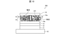
- Graphene has metallic conductivity. Therefore, if a layer containing graphene exists between the cathode and the anode, current will flow through the graphene, resulting in current leakage. In other words, a current leak path is formed.
- graphene does not have very high chemical stability. For this reason, graphene has the disadvantage that it is oxidized or decomposed, for example, during the operation of a light emitting element, and cannot maintain thermal conductivity or the above-mentioned barrier performance.
- a light-emitting device includes at least one light-emitting element described above according to one embodiment of the present disclosure.
- a highly reliable light emitting element and device that has improved thermal diffusivity than before without increasing non-radiative recombination and exciton quenching;
- a method for manufacturing a light emitting element can be provided.
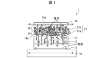
- FIG. 1 is a cross-sectional view schematically showing an example of a light emitting element according to Embodiment 1.
- FIG. FIG. 2 is a diagram schematically showing the crystal structure of c-BN nanoparticles.
- FIG. 2 is a diagram schematically showing the crystal structure of h-BN nanoparticles.
- 2 is a flowchart showing a method for manufacturing the light emitting device shown in FIG. 1.
- FIG. FIG. 6 is a diagram illustrating the accumulation of Joule heat due to the low thermal conductivity of each layer in a comparative light emitting element in which a layer containing the first material is not provided between the anode and the cathode. It is a graph which shows the relationship between the heating temperature of a quantum dot thin film, and PLQY.
- FIG. 9 is a diagram showing an optical microscope image of the quantum dots used in FIG. 8 after element leakage occurs due to local heat accumulation.
- FIG. 3 is a diagram illustrating problems of a comparative light emitting element using graphene as a first material for comparison.
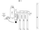
- FIG. 11 is a diagram showing the energy bands of each layer of the comparative light emitting element shown in FIG. 10 together with the energy band of BN. 3 is a cross-sectional view schematically showing an example of a light emitting element according to Embodiment 2.
- FIG. 7 is a cross-sectional view schematically showing an example of a method for forming a layer containing a first material in a light emitting device according to a second embodiment.
- FIG. FIG. 6 is a diagram illustrating a problem with impurity migration in a comparative light emitting element in which a layer containing a first material is not provided between an anode and a cathode. It is a figure which shows the result of measuring the element contained in the quantum dot layer from the cathode of the light emitting element in which the layer containing the 1st material is not provided between the anode and the cathode by AES.
- FIG. 16 is a graph showing the relationship between evaporation rate, driving voltage, and luminance when a light-emitting element having the same configuration as the light-emitting element used in the measurement shown in FIG. 15 is manufactured by changing the evaporation rate of the cathode (Ag). .
- FIG. 15 is a graph showing the relationship between the evaporation rate, drive voltage, and current density of the drive current when a light-emitting element having the same configuration as the light-emitting element used in the measurement shown in FIG. 15 was fabricated by changing the Ag evaporation rate. be.
- FIG. 16 is a graph showing the relationship between the vapor deposition rate, the current density of the drive current, and the brightness when a light emitting device having the same configuration as the light emitting device used in the measurement shown in FIG. 15 is fabricated by changing the Ag vapor deposition rate.
- FIG. . A graph showing the relationship between the evaporation rate, the current density of the driving current, and the external quantum efficiency when a light-emitting device having the same configuration as the light-emitting device used in the measurements shown in FIG. 15 was fabricated by changing the Ag deposition rate. It is.
- FIG. 16 is a diagram showing an EL emission image of a light emitting device having the same configuration as the light emitting device used in the measurements shown in FIG.
- a layer formed in a process earlier than the layer to be compared will be referred to as a "lower layer”
- a layer formed in a process after the layer to be compared will be referred to as an "upper layer”.
- the description "A to B" regarding the two numbers A and B means “more than A and less than B" unless otherwise specified.
- a light emitting element includes a first electrode, a second electrode, and at least one functional layer provided between the first electrode and the second electrode.
- the at least one functional layer includes a layer containing a material (hereinafter referred to as "first material") having a band gap (Eg) of 3.0 eV or more and a thermal conductivity of 200 W/mK or more.
- first material a material having a band gap (Eg) of 3.0 eV or more and a thermal conductivity of 200 W/mK or more.
- the material used to improve thermal diffusivity is referred to as the "first material”
- the first electrode is conventionally used for purposes other than thermal diffusion. This is distinguished from functional materials such as light-emitting materials and charge-transporting materials, which are originally included in the functional layer between the electrode and the second electrode.
- the at least one functional layer may include only one layer or multiple layers containing the first material. Therefore, a light emitting element according to one aspect of the present disclosure has a configuration in which at least one layer containing the first material is provided between the first electrode and the second electrode.
- the light emitting element By providing the light emitting element with at least one layer containing the first material between the first electrode and the second electrode, the light emitting element can be heated more efficiently than before without increasing non-radiative recombination and exciton quenching.
- a highly reliable light emitting element with improved diffusivity can be provided.
- the layer between the first electrode and the second electrode is referred to as a functional layer.
- the functional layer includes at least a light emitting layer.
- the “emitting layer” will be referred to as "EML”.
- the light emitting element can extract light emitted by EML from the transparent electrode side. Therefore, a translucent electrode is used for at least one of the anode and the cathode. Although each of these pair of electrodes may be a light-transmitting electrode, it is desirable that one of them is a so-called reflective electrode having light-reflecting properties. In this case, the light emitting element may be of a bottom emission type or a top emission type, but is more preferably a bottom emission type.
- the above light emitting element can be suitably used as a light source of a light emitting device such as a display device or a lighting device, for example.
- a light emitting device such as a display device or a lighting device
- a thick metal electrode that functions as a heat bath with a large heat capacity can be used as an upper layer electrode used as a common electrode in the light emitting device. Therefore, by making the light emitting element a bottom emission type light emitting element, it is possible to provide a light emitting element that has better heat dissipation properties for the heat diffused by the first material and is more effective in suppressing temperature rise.
- the above-mentioned light emitting element may be a single layer type including only one EML as a functional layer, or may be a multilayer type including a plurality of functional layers as a functional layer.
- EML includes the first material.
- the first material may be included only in the EML or only in the functional layer other than the EML. Further, the first material may be contained in both the EML and a functional layer other than the EML.
- the first material is contained only in some of the functional layers. It may be included in all functional layers. When the first material is contained in only some of the functional layers, the first material may be contained in only one of the functional layers, as described above, or in all the functional layers. It may be included in two or more arbitrary functional layers.
- the light emitting element may include at least an EML between the first electrode and the second electrode, and at least the EML may include the first material.
- the light emitting element may include at least one charge transport layer between the first electrode and the second electrode as a functional layer other than EML. That is, the light emitting element has an EML between the first electrode and the second electrode, and a charge transport layer between at least one of the first electrode and the EML and the second electrode and the EML. may be provided. and at least one layer of the charge transport layer (that is, the charge transport layer provided between the first electrode and the EML and between the second electrode and the EML) and the EML. may contain the first material.
- the light emitting element When the light emitting element includes a charge transport layer as a functional layer other than EML, the light emitting element may include only a hole transport layer or only an electron transport layer as a charge transport layer. Furthermore, the light emitting device may include both a hole transport layer and an electron transport layer as the charge transport layer.
- the hole transport layer will be referred to as "HTL” and the electron transport layer will be referred to as "ETL”.
- the first material when the light emitting element includes an HTL, the first material may be included in the HTL.
- the HTL is provided between the anode and the EML.
- the first material when the light emitting element includes an ETL, the first material may be included in the ETL.
- the ETL is provided between the cathode and the EML.
- the first material when the light emitting element includes an HTL and an ETL, the first material may be included only in the HTL, only in the ETL, or in both the HTL and the ETL. It may be
- the light emitting element may include a charge injection layer as a functional layer other than EML.
- the charge injection layer may be a hole injection layer or an electron injection layer.
- HIL hole injection layer
- EIL electron injection layer
- the first material when the light emitting element includes a HIL, the first material may be included in the HIL.
- the HIL is provided between the anode and the HTL.
- the first material when the light emitting element includes an EIL, the first material may be included in the EIL.
- the EIL is provided between the cathode and the ETL.
- the first material when the light emitting element includes a HIL and an EIL, the first material may be included only in the HIL, only in the EIL, or in both the HIL and the EIL. It may be
- the first material is contained only in one of the plurality of functional layers. It may be Therefore, when the light emitting element includes a charge injection layer as described above, the first material may be contained only in the charge injection layer, or may be contained in a plurality of functional layers including the charge injection layer. good.
- the functional layer other than EML may be a first material layer made of only the first material. Therefore, the functional layer between the first electrode and the second electrode may include at least one first material layer made of the first material in order to improve thermal diffusivity.
- the functional layer may include functional layers other than the EML, such as an electron injection layer, an electron blocking layer, a hole blocking layer, and the like.
- the light emitting element 1 is a bottom emission type light emitting element having a conventional structure in which the anode 11 is the lower electrode and the cathode 16 is the upper electrode.
- the light emitting element according to one embodiment of the present disclosure is not limited to this, and may have an inverted structure in which the cathode 16 is the lower electrode and the anode 11 is the upper electrode. Alternatively, it may be a top emission type light emitting element.
- the light emitting element 1 shown in FIG. 1 includes an anode 11, a HIL 12, an HTL 13, an EML 14, an ETL 15, and a cathode 16 in this order from the lower layer side.
- the substrate 10 may be, for example, a rigid inorganic substrate such as a glass substrate, or a flexible substrate whose main component is a resin such as polyimide. Note that the substrate 10 may be provided with a TFT (thin film transistor), a capacitive element, etc. (not shown).
- TFT thin film transistor
- the anode 11 is an electrode that supplies holes to the EML 14 when a voltage is applied.
- the cathode 16 is an electrode that supplies electrons to the EML 14 when a voltage is applied.
- the anode 11 and the cathode 16 each contain a conductive material, and are connected to a power source (not shown) so that a voltage is applied between them.
- the light emitting element 1 is, for example, a bottom emission type light emitting element, and uses a transparent electrode for the anode 11 and a reflective electrode for the cathode 16.
- the HIL 12 is a charge injection layer that includes a hole transporting material and has a hole injection function that increases the efficiency of hole injection from the anode 11 to the HTL 13.
- the hole-transporting material include a composite of poly(3,4-ethylenedioxythiophene) (PEDOT) and polystyrene sulfonic acid (PSS) (PEDOT:PSS).
- the HTL 13 is a charge transport layer that includes a hole transport material and has a hole transport function that increases the efficiency of hole transport to the EML 14.
- the hole-transporting material include poly[N,N'-bis(4-butylphenyl)-N,N'-bis(phenyl)-benzidine] (abbreviation: p-TPD), poly[(9 , 9-dioctylfluorenyl-2,7-diyl)-co-(4,4'-(N-4-sec-butylphenyl))diphenylamine)] (abbreviation: TFB).
- the emission wavelength of QD14a can be changed in various ways depending on the particle size, composition, etc. of the particles.
- the QDs 14a are QDs that emit visible light, and the emission wavelength can be controlled by appropriately adjusting the particle size and composition of the QDs 14a.
- the ETL 15 is a charge transport layer that contains an electron transport material and has an electron transport function that increases electron transport efficiency to the EML 14. Nanoparticles 15a having electron transport properties are used as the electron transport material.
- nanoparticles 15a examples include nanoparticles of ZnO, MgZnO, etc. Among them, ZnO nanoparticles (hereinafter referred to as "ZnO-NP”) are generally used.
- the light emitting element 1 includes at least one layer containing the first material 21 between the anode 11 and the cathode 16, thereby preventing non-radiative recombination and exciton quenching, as described above. It is possible to provide a highly reliable light emitting element 1 with improved thermal diffusivity compared to the conventional one without increasing . As shown in FIG. 1, all the functional layers between the anode 11 and the cathode 16 contain the first material 21, thereby further improving thermal diffusivity and providing a more reliable light emitting device 1. can do.
- Eg is less than 3.0 eV or the thermal conductivity is less than 100 W/mK, the above-mentioned effects cannot be sufficiently obtained. In particular, if Eg is less than 3.0 eV, non-radiative recombination and exciton quenching may occur.
- the upper limit of the thermal conductivity is not particularly limited, and is preferably as high as possible.
- the thermal conductivity of diamond which is generally said to have high thermal conductivity, is 1000 to 2000 W/mK.
- the thermal conductivity of carbon nanotubes, which is said to exceed that of diamond is said to be 3000 W/mK.
- the thermal conductivity of the first material 21 is currently 3000 W/mK or less, and generally 2000 W/mK or less. I can say that there is.
- the higher the upper limit of the thermal conductivity the more desirable. Therefore, it goes without saying that if there is a first material 21 having a thermal conductivity exceeding 3000 W/mK, such a first material 21 may be used.
- Eg was measured using a spectrophotometer "U-3900" (model) manufactured by Hitachi High-Tech Science Co., Ltd. Eg changes depending on manufacturing conditions, particle size of nanoparticles, etc. For example, if the materials and crystal systems are the same, the Eg increases as the particle size of the nanoparticles decreases. If Eg cannot be measured with the above-mentioned measuring device, a publicly available value, such as specifications listed in a catalog, may be used.
- the first material 21 has a VBM value larger (deeper) than the valence band upper end (VBM) value of the QD 14a, and a smaller (shallower) CBM value than the conduction band lower end (CBM) value of the QD 14a. It is enough if you have it. However, in order to sufficiently suppress non-radiative recombination and exciton quenching, it is desirable to have an Eg of 3.0 eV or more as described above. Further, the first material 21 has a VBM value larger than the value of the valence band upper end (VBM) of the ETL 15 such as ZnO-NP, and smaller (shallower) than the conduction band lower end (CBM) value of the HTL 13.
- VBM indicates the absolute value of the difference between the electron energy levels at the vacuum level and the VBM.
- CBM indicates the absolute value of the difference in the energy level of electrons between the vacuum level and the CBM.
- the EML 14 includes the first material 21
- the larger Eg is, the higher the carrier confinement effect is, and the luminous efficiency can be improved.
- carriers that should gather in a QD layer such as EML14 escape to a layer with a small Eg around the QD layer (that is, carrier diffusion).
- the periphery of the QD layer is not limited to the layer adjacent to the QD layer. For example, even in the case of a stacked structure such as QD layer/thin HTL/small Eg layer/HTL/HIL, carrier diffusion may occur.
- the functional layer is a functional layer other than the QD layer, if the Eg of the functional layer is large, carriers will not diffuse into the functional layer, and the luminous efficiency can be improved. Therefore, regardless of which functional layer the first material 21 is included in, it is preferable that the first material 21 has a larger Eg.
- the upper limit of Eg is also preferably as large as possible, and is not particularly limited.
- the first material 21 having Eg of 3.0 eV or more is an insulator.
- An example of a generally known insulator with a large Eg is SiO 2 .
- Eg of SiO 2 is 8.9 eV. Therefore, the upper limit of Eg can be considered to be approximately 9 eV, preferably 10 eV, at present.
- the thermal conductivity of the first material 21 is currently 3000 W/mK or less, and generally can be said to be 2000 W/mK or less.
- the higher the upper limit of Eg the more desirable. Therefore, it goes without saying that if there is a first material 21 having Eg exceeding 10 eV, such a first material 21 may be used.
- the first material 21 may be included in any functional layer between the anode 11 and the cathode 16, or may be included in the charge injection layer, for example, the HIL 12.
- the HIL 12 includes the first material 21
- the content of the first material 21 in the HIL 12 is desirably 25% or more and 80% or less in terms of cross-sectional area ratio of the HIL 12, and preferably 45% or more and 80% or less. is more desirable. This increases the thermal conductivity of the HIL 12 provided between the EML 14 and the anode 11, improves thermal diffusivity, and suppresses local heat concentration. 1 can be reduced.
- the content rate of the first material 21 in each functional layer is equal to the cross-sectional area ratio of each functional layer. is preferably 25% or more and 80% or less, more preferably 45% or more and 80% or less.
- the thermal conductivity of the functional layer containing the first material 21 is increased and the thermal diffusivity is improved. Local heat concentration can be suppressed. As a result, deterioration of the QD 14a and, by extension, deterioration of the light emitting element 1 can be reduced. Further, by setting the content of the first material 21 to 45% or more and 80% or less in terms of the cross-sectional area ratio, thermal diffusivity can be dramatically improved. Note that the above effects will be explained in more detail later using specific examples.
- the cross-sectional area ratio of the first material 21 is expressed by the following formula (1) (Cross-sectional area of the entire first material 21 in the layer containing the first material 21/cross-sectional area of the entire layer containing the first material 21) x 100%... (1) It can be found by
- the cross-sectional area ratio of the first material 21 can be determined, for example, by checking an electron microscope image of a cross-section of a layer containing the first material 21. It can be determined from the area ratio with the part.
- the cross-sectional area ratio of the first material 21 is determined by, for example, using a transmission electron microscope (TEM) and determining the cross-sectional area ratio of the layer containing the first material 21 in a TEM cross-sectional image of layer thickness of interest x 200 nm. It can be determined by calculating the area ratio of the first material 21.
- TEM transmission electron microscope
- a tiltable TEM is used to calculate, for example, the volume ratio of the first material 21 within a region of layer thickness of interest x 200 nm (length) x 100 nm (thickness).
- a method of calculating from a hologram image formed from TEM images taken from a plurality of angles may be used.
- the volume ratio of the first material 21 in the layer containing the first material 21 can be determined by the above-mentioned formula (2) similarly to the cross-sectional area ratio.
- BN has several crystal structures.
- c-BN cubic boron nitride
- h-BN hexagonal boron nitride
- h-BN has a crystal structure shown in FIG. 3.
- Bulk h-BN has a structure in which monoatomic layers of h-BN are weakly bonded on the c-axis.
- Bulk h-BN can be separated into a single layer or several atomic layers of h-BN by peeling off the crystal with tape or the like.
- h-BN separated into a single layer or several atomic layers will be referred to as "h-BN nanosheet.”
- h-BN nanosheets e.g., single-layer h-BN
- Conductivity is significantly different.
- the thermal conductivity (k ⁇ ) of a single layer of h-BN in the stacking direction of h-BN nanosheets, which is the direction perpendicular to the film surface (film thickness direction) is about 30 W/mK.
- the thermal conductivity (k // ) of a single layer of h-BN in a direction parallel to the main surface of the h-BN nanosheet, which is the film surface direction, is 600 W/mK.
- the Eg of the h-BN nanosheet is 6.0 eV.
- the Eg of QD14a is larger as the emission peak wavelength is shorter.
- the blue pixel with the shortest emission peak wavelength has QD14a that emits blue light is used.
- Eg of the QD14a that emits blue light is about 2.7 eV. Therefore, if Eg is 3.0 eV or more, exciton emission in the luminescent material will not be inhibited, regardless of the type of QD 14a. If the thermal conductivity is 200 W/mK or more, sufficient thermal conductivity can be ensured even when mixed with a low first material.
- thermal conductivity of the mixture K can be determined using the above equation (3).
- each functional layer includes both c-BN nanoparticles 21a and h-BN nanosheets 21b.
- each functional layer may include only either c-BN nanoparticles 21a or h-BN nanosheets 21b.
- the h-BN nanosheet 21b is an insulator.
- the above average film thickness of the h-BN nanosheets 21b is, for example, the average thickness of the h-BN nanosheets in the layer containing the h-BN nanosheets 21b in a TEM cross-sectional image of layer thickness of interest x 200 nm using TEM. It can be calculated by calculating the average film thickness of 21b.
- a method for manufacturing a light emitting element includes a step of forming a first electrode and a step of forming a second electrode, a step of forming the first electrode and a step of forming the second electrode. A step of forming a layer containing the first material 21 between the two steps is included.
- FIG. 4 is a flowchart showing a method for manufacturing the light emitting device 1 shown in FIG. 1.
- the light emitting device 1 shown in FIG. Contains.
- the anode 11 is formed on the substrate 10 (step S1).
- a plurality of functional layers are formed on the anode 11. Specifically, as shown in FIG. 4, first, a HIL 12 containing the first material 21 is formed as a functional layer (step S2). Next, HTL 13 including first material 21 is formed (step S3). Next, an EML 14 including the first material 21 is formed (step S4). Next, an ETL 15 including the first material 21 is formed (step S5). Note that in the light emitting element 1 shown in FIG. 1, as described above, the case where the HIL 12, HTL 13, EML 14, and ETL 15 each include the first material 21 is illustrated as an example.
- the light emitting element 1 only needs to include at least one layer containing the first material 21 between the anode 11 and the cathode 16. Therefore, in the step of forming the functional layer, at least one layer containing the first material 21 may be formed.
- the cathode 16 is formed (step S6).
- the light emitting element 1 shown in FIG. 1 is formed.
- the thermal conductivity of the layer in which each of the first materials 21 is mixed is greatly improved, and deterioration of each layer due to heat accumulation (specifically, deterioration of the constituent material of each layer) can be avoided, especially. Deterioration of the QD 14a in the EML 14 can be suppressed, and reliability can be improved.
- the method of forming the anode 11 and the cathode 16 is the same as the conventional method.
- the anode 11 and the cathode 16 can be formed by, for example, a vapor deposition method, a sputtering method, an inkjet method, or the like.
- Each functional layer constituting the light emitting element 1 can be formed by coating.
- a spin coating method, a vacuum evaporation method, an inkjet method, an imprint method, or the like can be used to form each functional layer.
- the HIL 12 can be formed by applying a dispersion containing an HIL material such as PEDOT:PSS and the first material 21 onto the anode 11, and then baking to volatilize the solvent.
- the HTL 13 can be formed by applying a dispersion containing an HTL material such as TFB and the first material 21 onto the HIL 12, and then baking to evaporate the solvent.
- the EML 14 can be formed by applying a dispersion containing the QDs 14a and the first material 21 onto the HTL 13, and then baking to evaporate the solvent.
- the ETL 15 can be formed by applying a dispersion containing nanoparticles 15a such as ZnO-NP, which are used as an ETL material, and the first material 21 onto the EML 14, and then baking to evaporate the solvent. can.
- the dispersion liquid used to form the EML 14 may contain a ligand as described above. Furthermore, the dispersion liquid used to form the ETL 15 may also contain a ligand in order to improve the dispersibility of the nanoparticles 15a. Moreover, in order to adjust the dispersibility of the first material 21 in the solvent at this time, a ligand may be included on the surface of the first material 21.
- the first materials 21 included in these HIL12, HTL13, EML14, and ETL15 may be the same or different. Furthermore, the ligands contained in EML14 and ETL15 may be the same or different.
- a polar solvent can be used as the coating solvent contained in each dispersion liquid used to form these functional layers.
- the polar solvent refers to a solvent having a dielectric constant of 10 or more.
- the solvent include ethanol, methanol, water, and the like.
- c-BN nanoparticles 21a and h-BN nanosheets 21b are preferably used as the first material 21.
- These c-BN nanoparticles 21a and h-BN nanosheets 21b can also be dispersed in a polar solvent. For this reason, by coating and forming a film by dispersing the material of each functional layer and, for example, these BN in an arbitrary ratio, a functional layer having an arbitrary BN mixing ratio can be formed. be able to.
- the c-axis direction of the crystal of the h-BN nanosheet 21b is oriented in a random direction.
- the h-BN nanosheet 21b it is possible for the h-BN nanosheet 21b to orient the c-axis direction of the crystal in a certain direction with a certain probability.
- the dispersion it is possible to intentionally orient the h-BN nanosheets 21b in a specific direction by applying an external force in a specific direction, for example.
- the c-BN nanoparticles 21a do not have anisotropy, and there is no particular need for alignment.
- each functional layer When the material of each functional layer is mixed with BN such as c-BN nanoparticles 21a and h-BN nanosheets 21b, the c-axis directions of the crystals of h-BN nanosheets 21b are oriented in random directions. . Therefore, the h-BN nanosheets 21b in each dispersion are randomly oriented. Therefore, for example, when each dispersion liquid is formed into a film, the h-BN nanosheets 21b are formed into a functional layer in which the h-BN nanosheets 21b are randomly oriented by performing the film formation under conditions where the flow of the dispersion liquid is small.
- a light emitting element called a QLED includes a QD layer as an EML.
- the QD layer accounts for most of the resistance, and it is thought that heat generation during driving is mainly generated from the QD layer. .
- FIG. 5 is a diagram illustrating the accumulation of Joule heat due to the low thermal conductivity of each layer in a comparative light emitting device 100 in which a layer containing the first material 21 is not provided between the anode 11 and the cathode 16. be.
- FIG. 5 shows, as an example, a case where the light emitting element 100 includes an anode 11, a HIL 12, an HTL 13, an EML 14, an ETL 15, and a cathode 16 in this order from the lower layer side on the substrate 10.
- the light emitting device 100 for comparison has the same configuration as the light emitting device 1 shown in FIG. 1, except that neither of the functional layers between the anode 11 and the cathode 16 includes the first material 21. .
- the thermal conductivity of the QD 14a is usually less than 1 W/m ⁇ K (for example, 0.3 W/m ⁇ K or less).
- the HTL 13 and ETL 15, which are the upper and lower layers of the EML 14, which is a QD layer, are also generally made of materials whose thermal conductivity is significantly lower than 20 W/m ⁇ K.
- ZnO-NP is generally used for the ETL 15, but the crystal grains of the nanoparticles are finer than the bulk, and phonon scattering occurs at the interface. Furthermore, compared to crystal grains inside the bulk, nanoparticles do not have sufficient contact with each other and have voids, making it difficult for heat to transfer. Therefore, although the thermal conductivity of the ZnO bulk is 20 W/m ⁇ K, the thermal conductivity of the ZnO-NP layer is considered to be significantly lower than that.
- the HTL 13 uses, for example, p-TPD or TFB. Therefore, the thermal conductivity of HTL13 is considered to be less than 0.3 W/m ⁇ K, which is equivalent to that of epoxy resin, acrylic resin, and the like.
- HIL12 organic materials are often used for HIL12.
- the HIL 12 uses, for example, PEDOT:PSS. Therefore, the thermal conductivity of HIL12 is also considered to be less than 0.3 W/m ⁇ K.
- the QD layer sandwiched between these functional layers is susceptible to accumulation of Joule heat during current injection, as shown in Figure 5, and in the current device configuration, heat generated locally in the QD layer is likely to accumulate. cannot be efficiently released from the QD layer. For this reason, the QD layer tends to rapidly deteriorate when emitting high-intensity light.
- the thermal conductivity of the ETL 15 can be improved, the thermal diffusivity between the QD layer and the cathode 16 can be increased, and heat can be released from the QD layer. becomes possible.
- the lower layer of the QD layer when ITO is used for the anode, which is the lower layer electrode, in a bottom emission type light emitting device, it has electrical conductivity, although the thermal conductivity is far from that of the metal film as described above. There is a lower electrode and a substrate 10 made of ITO. Therefore, even on the lower layer side of the QD layer, the thermal conductivity of the functional layer between the EML 14 and the anode 11 is improved, and as shown in FIG. 1, for example, the thermal diffusivity of the QD layer, HTL 13, HIL 12, etc. In this case, it becomes possible to sufficiently release heat from the QD layer. Further, at this time, the ITO film thickness may be reduced, for example, to 50 nm or less, in order to improve thermal diffusivity.
- FIG. 6 shows the results of measuring PLQY as an optical characteristic of the light emitting element, and shows the relationship between the heating temperature and PLQY of a single film of QD14a, which is a quantum dot thin film.
- FIG. 7 shows the results of measuring the PL emission lifetime as an optical property of a single film of the QD14a, which is a quantum dot thin film, and shows the relationship between the heating temperature of the QD14a single film and the PL emission lifetime.
- PL emission life refers to "the time until the PL emission intensity becomes 1/e of the initial intensity", and when a defect occurs, the lifetime is shortened due to the occurrence of a non-emission transition. Theoretically, this "PL luminescence lifetime" has a proportional relationship with luminous efficiency when measured with the same QD.
- the deterioration of the QDs 14a is not linear, but as the heating temperature rises from room temperature, the deterioration of the QDs 14a progresses exponentially.
- FIG. 8 is a graph showing the results of a reliability test of a comparative light-emitting element manufactured as a light-emitting element for evaluation.
- a light emitting element for evaluation was produced by the following method. First, an ITO film with a thickness of 30 nm was formed as an anode on a glass substrate. Next, a dispersion of NiO (nickel oxide) dispersed in ethanol was applied onto the ITO film and baked in the air for 1 hour to volatilize the solvent. As a result, a NiO layer with a thickness of 43 nm was formed as the HTL. Thereafter, a mixture of polymethyl methacrylate (abbreviation: PMMA) in acetone at a ratio of 0.9 mg/ml was applied to form a PMMA layer on the NiO.
- PMMA polymethyl methacrylate
- a dispersion containing CdSe as QDs was applied onto the PMMA layer and baked to evaporate the solvent.
- a QD layer having a thickness of 44 nm and emitting green light was formed.
- a dispersion containing ZnO-NPs with a diameter of 12 nm was applied onto the QD layer and baked to evaporate the solvent, thereby forming a ZnO-NP layer with a thickness of 50 nm as an ETL.
- a 100 nm thick Al layer was formed as a cathode on the ZnO-NP layer.
- the increase in leakage current eventually grows into a large leakage path, and as a result, most of the current flowing to the light emitting element passes through the current leakage path, and the light emitting element may no longer emit light.
- Temperature-related deterioration of QDs is nonlinear with respect to temperature rise. Therefore, by suppressing heat concentration at the pinhole portion, etc., the reliability of the light emitting element as a whole is improved.
- FIG. 10 is a diagram illustrating problems of a comparative light emitting element 200 using graphene as a first material for comparison.
- FIG. 11 is a diagram showing the energy bands of each layer of the comparative light emitting element 200 shown in FIG. 10 together with the energy band of BN.
- the light emitting element 200 includes an anode 11, a HIL 12, an HTL 13, an EML 14, an ETL 15, and a cathode 16 in this order from the lower layer side on the substrate 10.
- a case where graphene is mixed in the ETL 15 is illustrated as an example.
- the present embodiment by suppressing the deterioration of the QD 14a during high-intensity light emission, it is possible to suppress a decrease in luminous efficiency during high-intensity emission. Furthermore, as mentioned above, by suppressing the deterioration of QD14a, it is possible to emit light with a long PL (photoluminescence) emission lifetime and high brightness, and a higher PLQY (photoluminescence quantum yield) is realized. can do.
- FIG. 1 shows an example in which the c-axis directions of the crystals of the h-BN nanosheets 21b are oriented in random directions.
- the h-BN nanosheets 21b oriented in random directions include, for example, the h-BN nanosheets 21b in which the c-axis direction of the crystal is oriented in the film thickness direction.
- the functional layer includes, for example, the h-BN nanosheets 21b in which the c-axis direction of the crystals is oriented in the film thickness direction, so that the h-BN nanosheets 21b can be It is possible to improve the thermal conductivity in the thickness direction of the containing layer and to significantly improve the thermal diffusivity in the thickness direction.
- the h-BN nanosheets 21b oriented in random directions also include, for example, h-BN nanosheets 21b in which the c-axis direction of the crystal is oriented in the direction of the film surface.
- the functional layer includes h-BN nanosheets 21b in which the crystal c-axis direction is oriented in the film surface direction
- the thermal conductivity in the film surface direction of the layer containing the h-BN nanosheets 21b is improved.
- the functional layer since the functional layer includes h-BN nanosheets 21b in which the c-axis direction of the crystals is oriented in the direction of the film surface, the barrier function can be significantly improved.
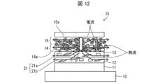
- FIG. 12 is a cross-sectional view schematically showing an example of the light emitting element 31 according to this embodiment.
- the h-BN nanosheets 21b can be formed with a certain probability depending on the film forming conditions by, for example, applying an external force in a specific direction when applying the dispersion containing the h-BN nanosheets 21b. It is possible to orient the c-axis direction of the crystal in a specific direction by a certain amount.
- the c-axis direction of most of the h-BN nanosheets 21b is oriented in the direction of the film surface of the functional layer containing the h-BN nanosheets 21b. Except for this point, the light emitting element 31 shown in FIG. 12 is the same as the light emitting element 1 shown in FIG. 1.
- a QD layer has a thinned part (for example, a pinhole)
- the QD layer becomes thinner during driving. Current flows preferentially to the exposed areas, making it easy for heat to accumulate. Therefore, by improving the thermal conductivity in the film surface direction of the light emitting element, it is possible to suppress the deterioration of the QD 14a and the light emitting element.
- FIG. 13 is a cross-sectional view schematically showing an example of a method for forming a layer containing the first material 21 in the light emitting element 31 according to the present embodiment.
- a QD layer that is, EML 14
- EML 14 is taken as an example of the layer containing the first material 21, and a part of the process of forming the QD layer is shown.
- the configuration shown in FIG. 12 can be achieved relatively easily using a solution process.
- in the step of forming a layer containing the first material 21, in order to orient the h-BN nanosheets 21b in the film surface direction, as shown in FIG. it is caused to flow in a direction parallel to the film surface direction of the HTL 13 which is the lower layer (underlying layer).
- the c-BN nanoparticles 21a and the h-BN nanosheets 21b can be dispersed in a polar solvent.
- the polar solvent described above can be used as the solvent 32 in the dispersion liquid 33.
- the material of each layer QD 14a in the example shown in FIG. 13
- the first material 21, and the solvent 32 are mixed into the material of each layer and the first material 21. and mix in any proportion.
- a dispersion liquid 33 containing the materials for each layer, the first material 21, and the solvent 32 is prepared.
- the viscosity of the dispersion liquid 33 is adjusted so that, for example, when the dispersion liquid 33 is dropped, the dispersion liquid 33 flows parallel to the direction of the lower layer film surface.
- the dispersion liquid 33 flows and spreads in parallel to the direction of the lower layer film surface due to the external force received by the drop. Due to the behavior of the h-BN nanosheets 21b when the dispersion liquid 33 falls and the flow of the h-BN nanosheets 21b due to the flow of the dispersion liquid 33, most of the h-BN nanosheets 21b in the dispersion liquid 33 are The film is oriented parallel to the surface direction of the film. Note that the direction of the lower layer film surface can be expressed as a direction parallel to the substrate surface or a direction parallel to the electrode surface. As a result, according to the present embodiment, the h-BN nanosheets 21b can be oriented in the direction of the film surface of the coating film formed by applying the dispersion liquid 33.
- the angle formed between the h-BN nanosheets 21b and a plane parallel to the film surface of the layer containing the h-BN nanosheets 21b refers to the angle between the cross section and the plane parallel to the film surface of the layer in cross-sectional observation. If the line of intersection is a straight line A, and the line of intersection between the cross section and the h-BN nanosheet 21b is a straight line B, this may mean the angle formed by the straight line A and the straight line B.
- the average value of the angle ⁇ of the cross section in the thickness direction of the layer containing the h-BN nanosheets 21b is more preferably 30 degrees or less, and even more preferably 15 degrees or less.
- the h-BN nanosheet 21b has high barrier properties in the direction perpendicular to the membrane surface, and can prevent oxygen molecules, water molecules, and other impurities from permeating in the direction perpendicular to the membrane surface. Therefore, by orienting the h-BN nanosheets 21b in the film surface direction of the layer containing the h-BN nanosheets 21b or in a direction close to the film surface direction, each Impurity diffusion in the stacking direction of the functional layers can be prevented.
- the h-BN nanosheets 21b when the h-BN nanosheets 21b are oriented in the film surface direction of each functional layer in this way, the h-BN nanosheets may have a size of 50 nm x 50 nm or more in the film inward direction. Preferably, it is more preferable that the size is 100 nm ⁇ 100 nm or more. In this way, since the h-BN nanosheet 21b has a sufficient size (in other words, a sufficient area) in the inward direction of the film, impurity diffusion can be suppressed more effectively.
- h-BN nanosheets having a size of 50 nm x 50 nm or more in the in-film direction means that the h-BN nanosheets include a 50 nm x 50 nm square within the sheet plane. Indicates that it has a large surface area. If one side is less than 50 nm, even if it has an area equivalent to 50 nm x 50 nm, it cannot be said that it has a size of 50 nm x 50 nm or more.
- h-BN nanosheets having a size of 100 nm x 100 nm or more in the in-film direction means that h-BN nanosheets only contain squares of 100 nm x 100 nm in the sheet plane. Indicates that it has a wide surface area.
- the h-BN nanosheet 21b has a size of 50 nm x 50 nm or more, preferably 100 nm x 100 nm or more in the inward direction of the film, a large area can be used as a barrier layer as one connected h- It can be covered with the BN nanosheet 21b. As a result, a high barrier effect can be exhibited.
- the size of the h-BN nanosheet 21b can be observed by the following method. For example, a TEM image using a tilt function using a tiltable TEM and the h-BN nanosheet 21b existing in a volume of the total stacked layer thickness of the light emitting element 31 x cutout piece thickness of 100 nm x length in the film surface direction of 200 nm Observe the size and configuration of. Thereby, the maximum size of the h-BN nanosheet 21b can be observed. Note that, similar to the observation of the volume ratio described above, a hologram image may be created and observed.
- the content rate of the first material 21 in the layer containing the first material 21 is 25% in terms of the cross-sectional area ratio of each layer. Above, it is desirable that it is 80% or less, and more preferably that it is 45% or more and 80% or less.
- Embodiment 1 the relationship between the cross-sectional area ratio and the effect of improving thermal conductivity was specifically explained using the case where c-BN nanoparticles 21a were used as the first material 21 as an example.
- h-BN nanosheets 21b are used as the first material 21
- similar effects can be obtained in the film surface direction.
- the thermal conductivity of ZnO-NP is 20 W/mK
- h-BN nanosheets 21b are mixed into the ZnO-NP layer at the cross-sectional area ratio of 25%, from the above equation (3), the heat in the film surface direction will increase.
- Conductivity can be improved approximately twice.
- the thermal conductivity in the film surface direction can be improved by about 3 times from the above formula (3). can.
- each functional layer contains both c-BN nanoparticles 21a and h-BN nanosheets 21b
- each functional layer contains only h-BN nanosheets. May contain.
- the first material 21 only needs to be mixed in at least one of the functional layers between the anode 11 and the cathode 16; It suffices to have at least one layer containing.
- the thermal conductivity in the film surface direction of the layer mixed with h-BN is significantly improved, and the thermal diffusivity is improved, thereby preventing local heat accumulation. It is possible to suppress deterioration due to Further, Eg is as explained in Embodiment 1, and according to this embodiment, thermal diffusivity is improved compared to the conventional one without increasing non-radiative recombination and exciton quenching. It is possible to provide a light emitting element 31 with a high luminance.
- the h-BN nanosheet 21b has a network structure in which B atoms and N atoms are densely arranged, and oxygen molecules, water molecules, and other Impurities can be prevented from passing through. Furthermore, the h-BN nanosheet 21b is provided between the anode 11 and the cathode 16. Therefore, according to the present embodiment, it is possible to provide the light emitting element 31 in which impurities are difficult to reach the QD layer and other functional layers during the manufacturing process and during driving.
- h-BN can further suppress the migration of impurities within the light emitting element 31, especially by mixing it into a layer made of nanoparticles with many voids. Thereby, deterioration related to impurities can be suppressed and reliability can be further improved. This will be explained in more detail below.
- FIG. 14 is a diagram illustrating the problem of impurity migration in the comparative light emitting element 100 in which the layer containing the first material 21 is not provided between the anode 11 and the cathode 16, as described above.
- the QD layers EML14 and ETL15 are composed of nanoparticles, and impurities can penetrate into the inside of the element through the gaps between the nanoparticles. It is.
- the gap between the ZnO-NPs is large enough to allow particles with a diameter of 1.24 nm to pass through even if the ZnO-NPs are closest packed. Since the diameter of oxygen molecules is 0.296 nm and the diameter of water molecules is 0.38 nm, oxygen molecules and water molecules pass through the gap between ZnO-NPs.
- oxygen and moisture in the atmosphere may enter the EML 14 from the outside via the ETL 15. Furthermore, during the manufacturing process of the light emitting element 31, a process solvent such as water may penetrate into the lower layer and enter the EML 14, degrading the QD 14a. Furthermore, residual solvent such as water diffuses into the EML 14 from the lower functional layer of the EML 14, such as the HIL 12 and HTL 13, which is provided between the anode 11 and the cathode 16.
- FIG. 15 shows Auger electron spectroscopy analysis of elements contained in the cathode 16, ETL 15, and EML 14 (QD layer) of a light emitting device in which a layer containing the first material 21 is not provided between the anode 11 and the cathode 16. It is a figure showing the result measured by (AES).
- a light emitting device manufactured by the following method was used in the above measurements. First, an ITO film with a thickness of 30 nm was formed as an anode on a glass substrate. Next, a 45 nm CuSCN layer was formed as a HIL on the ITO film. Next, a 40 nm P-TPD layer was formed as a HIL on the CuSCN layer. Next, a dispersion of red-emitting QDs containing Cd dispersed in octane was applied onto the P-TPD layer and baked to form a QD layer with a thickness of 30 nm.
- a 57 nm thick ZnO-NP layer made of ZnO-NPs with a diameter of 12 nm was formed as an ETL on the QD layer.
- a 100 nm thick Al layer was formed as a cathode on the ZnO-NP layer.
- FIG. 18 shows the current density J of the evaporation rate and drive current when a light-emitting element having the same configuration as the light-emitting element used in the measurement shown in FIG. 15 except for the electrodes was fabricated as a sample by changing the Ag evaporation rate. It is a graph showing the relationship between (mA/cm 2 ) and luminance L (cd/m 2 ).
- FIG. 19 shows the current density J of the evaporation rate and driving current when a light-emitting element having the same configuration as the light-emitting element used in the measurement shown in FIG.
- the h-BN nanosheet 21b has high barrier properties against impurities in the direction perpendicular to the film surface. Therefore, it is possible to prevent impurities from entering the inside of the element as described with reference to FIG. This suppresses deterioration of the QD 14a and also reduces the amount of water and oxygen inside the device from the viewpoint of long-term reliability.
- the incorporation of the h-BN nanosheets 21b oriented in the film plane direction into the functional layer, especially the incorporation into HTL13 and ETL15, is important for the metal atoms as described above during electrode creation. It is particularly effective in preventing intrusion.
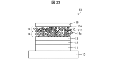
- FIG. 22 is a cross-sectional view schematically showing an example of the light emitting element 41 according to this embodiment. Further, FIG. 23 is a cross-sectional view schematically showing an example of the light emitting element 51 according to this embodiment.
- These light emitting elements 41 and 51 have the same configuration as the light emitting elements shown in Embodiment 1 or Embodiment 2, except for the following points.
- the layer containing the first material 21 may be formed as a single layer containing only the first material 21, and in any case, the layer containing the first material 21 may be formed between the anode 11 and the cathode 16.
- the same effects as those described in the first and second embodiments can be obtained.
- BN is an insulator, and if the thickness of the first material layer 22 exceeds 2 nm, there is a risk that tunnel current will no longer flow in the direction perpendicular to the film surface direction (film thickness direction). There is a risk that the voltage will be increased (higher resistance), making it difficult to use it as a light emitting element. For this reason, it is desirable that the layer thickness of the first material layer 22 be 2 nm or less.
- the light emitting element 51 shown in FIG. 23 includes, for example, an ETL 15 mixed with, for example, h-BN nanosheets 21b as the first material 21.
- an ETL 15 mixed with, for example, h-BN nanosheets 21b as the first material 21.
- h-BN nanosheets 21b do not have a large resistance, and the h-BN nanosheets 21b can be mixed into the ETL at a high volume ratio, and sufficient thermal conductivity in the film surface direction can be easily ensured. I can do it.
- the red pixel PR is provided with a red light emitting element that emits red light as a light emitting element.
- the green pixel PG is provided with a green light emitting element as a light emitting element.
- the blue pixel PB is provided with a blue light emitting element as a light emitting element.
- the red light emitting element has a structure in which an anode 11, a HIL 12, an HTL 13, an EML 14R, an ETL 15R, and a cathode 16 are stacked in this order on a substrate 10.
- the green light emitting element has a structure in which an anode 11, a HIL 12, an HTL 13, an EML 14G, an ETL 15G, and a cathode 16 are laminated in this order on a substrate 10.
- the blue light emitting element has a structure in which an anode 11, a HIL 12, an HTL 13, an EML 14B, an ETL 15B, and a cathode 16 are laminated in this order on a substrate 10.
- the EML 14R is a red EML that emits red light, and includes a red QD 14aR that emits red light as the QD 14a.
- the EML 14G is a green EML that emits green light, and includes a green QD 14aG that emits green light as the QD 14a.
- the EML 14B is a blue EML that emits blue light, and includes a blue QD 14aB that emits blue light as the QD 14a. Note that the same light emitting element (same pixel) includes the same type of QD 14a.
- the anode 11 functions as a so-called pixel electrode, and is provided in an island shape on the substrate 10 for each light emitting element (in other words, for each pixel).
- the cathode 16 is provided as a common electrode for all light emitting elements (in other words, all pixels). Each light emitting element functions as a light source that lights up each pixel.
- EML14R, EML14G, and EML14B are colored differently for each pixel, and are separated into islands by bank BK.
- ETL15R, ETL15G, and ETL15B are also painted differently for each pixel, and are separated into islands by bank BK.
- the bank BK is formed by, for example, applying an organic material such as polyimide or acrylic resin and then patterning it by photolithography.
- FIG. 24 as an example, a case is illustrated in which h-BN nanosheets 21b are mixed as the first material 21 only into ETL15R, ETL15G, and ETL15B.
- the light emission threshold voltage indicates the voltage at which the light emitting element starts emitting light when the voltage applied to the light emitting element is increased.
- the element structure is optimized, and in an ideal case, the light emission threshold voltage is This is the value obtained by converting Eg of .
- Eg of QD14a is Eg of QD14aR ⁇ Eg of QD14aG ⁇ Eg of QD14aB. Therefore, in this case, as shown in FIG. 15, the first material 21 in the cross-sectional area ratio of the layer containing the first material 21 in each light emitting element is arranged in the order of red light emitting element ⁇ green light emitting element ⁇ blue light emitting element. Increase the content rate.
- FIG. 24 shows an example in which the layer containing the first material 21 is the ETL 15, the layer containing the first material 21 may be a layer other than the ETL 15.
- the light emitting device is a full-color display device
- the present embodiment is not limited to this.
- the above technique can be applied to all light emitting devices having a plurality of light emitting elements having different emission peak wavelengths.
- the device includes a plurality of light emitting elements including a first light emitting element that emits light in a first wavelength band and a second light emitting element that emits light in a second wavelength band having a shorter emission peak wavelength than the first light emitting element.
- the content of the first material 21 in terms of the cross-sectional area ratio of the layer containing the first material 21 in the second light-emitting element is expressed as the content rate of the first material 21 in the cross-sectional area ratio of the layer containing the first material 21 in the first light-emitting element.
- the content rate may be greater than the content rate of the first material 21.
Landscapes
- Physics & Mathematics (AREA)
- Optics & Photonics (AREA)
- Engineering & Computer Science (AREA)
- Chemical & Material Sciences (AREA)
- Crystallography & Structural Chemistry (AREA)
- Inorganic Chemistry (AREA)
- Nanotechnology (AREA)
- Manufacturing & Machinery (AREA)
- Electroluminescent Light Sources (AREA)
Abstract
Description
本開示の一態様に係る発光素子は、第1電極と、第2電極と、上記第1電極と上記第2電極との間に設けられた少なくとも1層の機能層と、を備えている。そして、上記少なくとも1層の機能層が、3.0eV以上のバンドギャップ(Eg)および200W/mK以上の熱伝導率を有する材料(以下、「第1材料」と称する)を含む層を備えている。なお、本開示では、このように本開示で熱拡散性の改善に用いる材料(言わば熱拡散材料)を「第1材料」と称し、従来、熱拡散以外の目的で用いられる、上記第1電極と上記第2電極との間の機能層に本来含まれる、発光材料、電荷輸送材料等の機能材料と区別する。
図1は、本実施形態に係る発光素子1の一例を模式的に示す断面図である。
(第1材料21を含む層における第1材料21全体の断面積/第1材料21を含む層全体の断面積)×100%‥(1)
で求めることができる。
(第1材料21を含む層における第1材料21全体の断面積/第1材料21を含む層全体の断面積)×100%‥(2)
で求めてもよい。
K=Kf(1+2φA/1-φA)‥(3)
(但し、A=(1-Kf/Ks)(2Kf/Ks+1))
を適用することができる。
本開示の一態様に係る発光素子の製造方法は、第1電極を形成する工程と、第2電極を形成する工程と、を含み、第1電極を形成する工程と第2電極を形成する工程との間に、第1材料21を含む層を形成する工程を含む。
次に、上記発光素子1による効果について説明する。
図12は、本実施形態に係る発光素子31の一例を模式的に示す断面図である。
このようにh-BNナノシート21bが、その膜内方向に十分な大きさ(言い換えれば、十分な面積)を有することで、不純物拡散をより効果的に抑制することができる。
実施形態1、2では、第1材料21を、陽極11と陰極16との間に設けられた機能層の少なくとも1層に混入させることで、陽極11と陰極16との間に、第1材料21を含む層を少なくとも1層設ける場合を例に挙げて説明した。しかしながら、前述したように、上記機能層は、第1材料21からなる第1材料層を少なくとも1層含んでいてもよい。
前述したように、本開示の一態様に係る発光素子は、例えば、表示装置あるいは照明装置等の発光デバイスの光源として用いられてよい。
11 陽極(第1電極または第2電極)
12 HIL(機能層)
13 HTL(電荷輸送層、機能層)
14、14R、14G、14B EML(発光層)
14a、14aB、14aG、14aR QD
15、15R、15G、15B ETL(電荷輸送層、機能層)
15a ナノ粒子
16 陰極(第1電極または第2電極)
21 第1材料
21a c-BNナノ粒子
21b h-BNナノシート
22 第1材料層
61 表示装置
Claims (16)
- 第1電極と第2電極とを備え、
上記第1電極と上記第2電極との間に、3.0eV以上のバンドギャップおよび200W/mK以上の熱伝導率を有する第1材料を含む層が少なくとも1層設けられていることを特徴とする発光素子。 - 第1電極と第2電極とを備え、
上記第1電極と上記第2電極との間に、c-BNナノ粒子を含む第1材料を含む層が少なくとも1層設けられていることを特徴とする発光素子。 - 上記第1材料がh-BNナノシートをさらに含むことを特徴とする請求項2に記載の発光素子。
- 第1電極と第2電極とを備え、
上記第1電極と上記第2電極との間に、h-BNナノシートを含む第1材料を含む層が少なくとも1層設けられていることを特徴とする発光素子。 - 上記第1電極と上記第2電極との間に、量子ドットを含む発光層を少なくとも備え、
少なくとも上記発光層が上記第1材料を含むことを特徴とする請求項1~4の何れか1項に記載の発光素子。 - 上記第1電極と上記第2電極との間に、量子ドットを含む発光層を少なくとも備えるとともに、
上記第1電極と上記発光層との間、並びに、上記第2電極と上記発光層との間、の少なくとも一方に電荷輸送層を備え、
上記電荷輸送層、並びに、上記発光層、のうち少なくとも1層が上記第1材料を含むことを特徴とする請求項1~4の何れか1項に記載の発光素子。 - 上記第1電極と上記第2電極との間に複数層の機能層を備え、
上記複数層の機能層全てが上記第1材料を含むことを特徴とする請求項1~4の何れか1項に記載の発光素子。 - 上記第1材料を含む層における断面積比率での上記第1材料の含有率が、25%以上、80%以下であることを特徴とする請求項1~7の何れか1項に記載の発光素子。
- 上記第1材料を含む層の厚み方向の断面の単位面積当たりにおける上記h-BNナノシートの平均の膜厚が、2nm以下であることを特徴とする請求項3または4に記載の発光素子。
- 上記第1材料を含む層の厚み方向の断面の単位面積当たりにおける、上記第1材料を含む層の膜面に平行な面と上記h-BNナノシートとがなす角度の平均値が45度未満であることを特徴とする請求項3、4、9の何れか1項に記載の発光素子。
- 上記h-BNナノシートは、その膜内方向の大きさが50nm×50nm以上であることを特徴とする請求項3、4、9、10の何れか1項に記載の発光素子。
- 上記h-BNナノシートは、その膜内方向の大きさが100nm×100nm以上であることを特徴とする請求項3、4、9~11の何れか1項に記載の発光素子。
- 請求項1~12の何れか1項に記載の発光素子を少なくとも1つ備えていることを特徴とする発光デバイス。
- 上記発光素子として複数の発光素子を備えるとともに、
上記複数の発光素子は、第1波長帯域の光を発する第1発光素子と、上記第1発光素子よりも発光ピーク波長が短い第2波長帯域の光を発する第2発光素子とを含み、
上記第2発光素子における上記第1材料を含む層の断面積比率での上記第1材料の含有率が、上記第1発光素子における上記第1材料を含む層の断面積比率での上記第1材料の含有率よりも大きいことを特徴とする請求項13に記載の発光デバイス。 - 第1電極を形成する工程と、
第2電極を形成する工程と、を含み、
上記第1電極を形成する工程と上記第2電極を形成する工程との間に、
3.0eV以上のバンドギャップおよび200W/mK以上の熱伝導率を有する第1材料を含む層を形成する工程を含むことを特徴とする発光素子の製造方法。 - 上記第1材料を含む層を形成する工程では、上記第1材料を含む分散液を、該第1材料を含む層の下層の膜面方向に平行な方向に流動させることを特徴とする請求項15に記載の発光素子の製造方法。
Priority Applications (2)
| Application Number | Priority Date | Filing Date | Title |
|---|---|---|---|
| PCT/JP2022/023301 WO2023238331A1 (ja) | 2022-06-09 | 2022-06-09 | 発光素子、発光デバイス、および発光素子の製造方法 |
| US18/872,824 US20250374746A1 (en) | 2022-06-09 | 2022-06-09 | Light-emitting element, light-emitting device, and method for manufacturing light-emitting element |
Applications Claiming Priority (1)
| Application Number | Priority Date | Filing Date | Title |
|---|---|---|---|
| PCT/JP2022/023301 WO2023238331A1 (ja) | 2022-06-09 | 2022-06-09 | 発光素子、発光デバイス、および発光素子の製造方法 |
Publications (1)
| Publication Number | Publication Date |
|---|---|
| WO2023238331A1 true WO2023238331A1 (ja) | 2023-12-14 |
Family
ID=89117764
Family Applications (1)
| Application Number | Title | Priority Date | Filing Date |
|---|---|---|---|
| PCT/JP2022/023301 Ceased WO2023238331A1 (ja) | 2022-06-09 | 2022-06-09 | 発光素子、発光デバイス、および発光素子の製造方法 |
Country Status (2)
| Country | Link |
|---|---|
| US (1) | US20250374746A1 (ja) |
| WO (1) | WO2023238331A1 (ja) |
Citations (2)
| Publication number | Priority date | Publication date | Assignee | Title |
|---|---|---|---|---|
| US20150028365A1 (en) * | 2013-07-24 | 2015-01-29 | Juanita N. Kurtin | Highly refractive, transparent thermal conductors for better heat dissipation and light extraction in white leds |
| CN111200066A (zh) * | 2018-11-16 | 2020-05-26 | Tcl集团股份有限公司 | 一种量子点发光二极管及其制备方法 |
-
2022
- 2022-06-09 WO PCT/JP2022/023301 patent/WO2023238331A1/ja not_active Ceased
- 2022-06-09 US US18/872,824 patent/US20250374746A1/en active Pending
Patent Citations (2)
| Publication number | Priority date | Publication date | Assignee | Title |
|---|---|---|---|---|
| US20150028365A1 (en) * | 2013-07-24 | 2015-01-29 | Juanita N. Kurtin | Highly refractive, transparent thermal conductors for better heat dissipation and light extraction in white leds |
| CN111200066A (zh) * | 2018-11-16 | 2020-05-26 | Tcl集团股份有限公司 | 一种量子点发光二极管及其制备方法 |
Also Published As
| Publication number | Publication date |
|---|---|
| US20250374746A1 (en) | 2025-12-04 |
Similar Documents
| Publication | Publication Date | Title |
|---|---|---|
| US12010860B2 (en) | Quantum dot LED design based on resonant energy transfer | |
| Acharya et al. | High efficiency quantum dot light emitting diodes from positive aging | |
| Li et al. | Advances in understanding quantum dot light-emitting diodes | |
| US10403690B2 (en) | Light emitting device including tandem structure with quantum dots and nanoparticles | |
| US20080278063A1 (en) | Electroluminescent device having improved power distribution | |
| US7919342B2 (en) | Patterned inorganic LED device | |
| US11302883B2 (en) | Multiple-layer quantum-dot LED and method of fabricating same | |
| Wang et al. | High-performance azure blue quantum dot light-emitting diodes via doping PVK in emitting layer | |
| US20080237611A1 (en) | Electroluminescent device having improved contrast | |
| US20140264269A1 (en) | Tunable light emitting diode using graphene conjugated metal oxide semiconductor-graphene core-shell quantum dots and its fabrication process thereof | |
| Pan et al. | Flexible quantum dot light emitting diodes based on ZnO nanoparticles | |
| KR102607451B1 (ko) | 발광 소자 및 이를 포함하는 표시 장치 | |
| JP2005038634A (ja) | 電流注入型発光素子 | |
| KR101656927B1 (ko) | 발광 소자 및 발광 소자용 전자수송층 제조 방법 | |
| WO2024085101A1 (ja) | 発光素子および表示装置 | |
| KR101560088B1 (ko) | 발광 소자 및 발광 소자 제조 방법 | |
| WO2022227684A1 (zh) | 显示面板 | |
| WO2023238331A1 (ja) | 発光素子、発光デバイス、および発光素子の製造方法 | |
| JP2023551766A (ja) | ハイブリッド輸送層を有する電界発光デバイス | |
| Perveen | Investigation of sputtered gold nanoparticles substrates for surface plasmon enhanced electroluminescence and photoluminescence devices School of Physics Beijing Institute of Technology, Beijing China | |
| KR102723562B1 (ko) | 발광 필름 및 발광 소자 | |
| WO2025248707A1 (ja) | 発光素子、表示装置、発光素子の製造方法 | |
| WO2024241441A1 (ja) | 発光素子、発光素子の製造方法、および表示装置 |
Legal Events
| Date | Code | Title | Description |
|---|---|---|---|
| 121 | Ep: the epo has been informed by wipo that ep was designated in this application |
Ref document number: 22945833 Country of ref document: EP Kind code of ref document: A1 |
|
| WWE | Wipo information: entry into national phase |
Ref document number: 18872824 Country of ref document: US |
|
| NENP | Non-entry into the national phase |
Ref country code: DE |
|
| 122 | Ep: pct application non-entry in european phase |
Ref document number: 22945833 Country of ref document: EP Kind code of ref document: A1 |
|
| NENP | Non-entry into the national phase |
Ref country code: JP |
|
| WWP | Wipo information: published in national office |
Ref document number: 18872824 Country of ref document: US |