WO2023234172A1 - コンデンサアレイ - Google Patents
コンデンサアレイ Download PDFInfo
- Publication number
- WO2023234172A1 WO2023234172A1 PCT/JP2023/019514 JP2023019514W WO2023234172A1 WO 2023234172 A1 WO2023234172 A1 WO 2023234172A1 JP 2023019514 W JP2023019514 W JP 2023019514W WO 2023234172 A1 WO2023234172 A1 WO 2023234172A1
- Authority
- WO
- WIPO (PCT)
- Prior art keywords
- groove
- layer
- capacitor
- sealing layer
- capacitor array
- Prior art date
- Legal status (The legal status is an assumption and is not a legal conclusion. Google has not performed a legal analysis and makes no representation as to the accuracy of the status listed.)
- Ceased
Links
Images












Classifications
-
- H—ELECTRICITY
- H01—ELECTRIC ELEMENTS
- H01G—CAPACITORS; CAPACITORS, RECTIFIERS, DETECTORS, SWITCHING DEVICES, LIGHT-SENSITIVE OR TEMPERATURE-SENSITIVE DEVICES OF THE ELECTROLYTIC TYPE
- H01G9/00—Electrolytic capacitors, rectifiers, detectors, switching devices, light-sensitive or temperature-sensitive devices; Processes of their manufacture
- H01G9/26—Structural combinations of electrolytic capacitors, rectifiers, detectors, switching devices, light-sensitive or temperature-sensitive devices with each other
-
- H—ELECTRICITY
- H01—ELECTRIC ELEMENTS
- H01G—CAPACITORS; CAPACITORS, RECTIFIERS, DETECTORS, SWITCHING DEVICES, LIGHT-SENSITIVE OR TEMPERATURE-SENSITIVE DEVICES OF THE ELECTROLYTIC TYPE
- H01G9/00—Electrolytic capacitors, rectifiers, detectors, switching devices, light-sensitive or temperature-sensitive devices; Processes of their manufacture
- H01G9/004—Details
- H01G9/008—Terminals
- H01G9/012—Terminals specially adapted for solid capacitors
-
- H—ELECTRICITY
- H01—ELECTRIC ELEMENTS
- H01G—CAPACITORS; CAPACITORS, RECTIFIERS, DETECTORS, SWITCHING DEVICES, LIGHT-SENSITIVE OR TEMPERATURE-SENSITIVE DEVICES OF THE ELECTROLYTIC TYPE
- H01G9/00—Electrolytic capacitors, rectifiers, detectors, switching devices, light-sensitive or temperature-sensitive devices; Processes of their manufacture
- H01G9/004—Details
- H01G9/08—Housing; Encapsulation
-
- H—ELECTRICITY
- H01—ELECTRIC ELEMENTS
- H01G—CAPACITORS; CAPACITORS, RECTIFIERS, DETECTORS, SWITCHING DEVICES, LIGHT-SENSITIVE OR TEMPERATURE-SENSITIVE DEVICES OF THE ELECTROLYTIC TYPE
- H01G9/00—Electrolytic capacitors, rectifiers, detectors, switching devices, light-sensitive or temperature-sensitive devices; Processes of their manufacture
- H01G9/004—Details
- H01G9/08—Housing; Encapsulation
- H01G9/10—Sealing, e.g. of lead-in wires
-
- H—ELECTRICITY
- H01—ELECTRIC ELEMENTS
- H01G—CAPACITORS; CAPACITORS, RECTIFIERS, DETECTORS, SWITCHING DEVICES, LIGHT-SENSITIVE OR TEMPERATURE-SENSITIVE DEVICES OF THE ELECTROLYTIC TYPE
- H01G9/00—Electrolytic capacitors, rectifiers, detectors, switching devices, light-sensitive or temperature-sensitive devices; Processes of their manufacture
- H01G9/15—Solid electrolytic capacitors
-
- H—ELECTRICITY
- H01—ELECTRIC ELEMENTS
- H01G—CAPACITORS; CAPACITORS, RECTIFIERS, DETECTORS, SWITCHING DEVICES, LIGHT-SENSITIVE OR TEMPERATURE-SENSITIVE DEVICES OF THE ELECTROLYTIC TYPE
- H01G9/00—Electrolytic capacitors, rectifiers, detectors, switching devices, light-sensitive or temperature-sensitive devices; Processes of their manufacture
- H01G9/004—Details
- H01G9/04—Electrodes or formation of dielectric layers thereon
- H01G9/048—Electrodes or formation of dielectric layers thereon characterised by their structure
Definitions
- the present invention relates to a capacitor array.
- Patent Document 1 describes that before solid electrolytic capacitors are formed on a chemically formed aluminum foil sheet, one side of the chemically formed aluminum foil is separated and divided by dry machining using a laser device or a mold. After forming a groove and further forming a protective insulating material on the same surface that also serves as a reinforcing material for the sheet, a solid electrolytic capacitor is formed, and then the chemically formed aluminum foil is shaved off from the back surface until the bottom of the groove is exposed.
- a method for manufacturing a component-embedded board is disclosed in which a solid electrolytic capacitor and a wiring pattern are electrically separated and formed on a chemically formed aluminum foil sheet.
- a separation groove and a protective insulating material are formed on one side of a chemically formed aluminum foil.
- the resulting component-embedded substrate has an asymmetrical structure on the front and back, and is therefore prone to warping.
- stress tends to be concentrated at the intersection of the grooves due to the above-mentioned warpage, so that separation (delamination) between the materials is likely to occur.
- the present inventors considered manufacturing a capacitor array having a symmetrical structure on the front and back.
- An object of the present invention is to provide a capacitor array in which a plurality of capacitor elements are divided by through grooves that intersect with each other, in which short-circuit defects occurring between adjacent capacitor elements can be reduced. .
- the capacitor array of the present invention includes a capacitor layer including a plurality of capacitor elements arranged in a plane in a plane direction perpendicular to the thickness direction by being divided by a plurality of through grooves.
- Each of the capacitor elements includes a first electrode layer, a second electrode layer, and a dielectric layer, and the first electrode layer and the second electrode layer face each other in the thickness direction with the dielectric layer interposed therebetween.
- the through groove includes a first through groove extending in a first direction and a second through groove extending in a second direction intersecting the first direction.
- the present invention it is possible to provide a capacitor array in which a plurality of capacitor elements are divided by mutually intersecting through grooves, in which short-circuit defects occurring between adjacent capacitor elements can be reduced.
- FIG. 1 is a schematic perspective view showing an example of a capacitor array of the present invention.
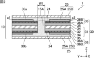
- FIG. 2 is a schematic cross-sectional view showing an example of a cross section of a capacitor array including a cross section along line segment a1-a2 in FIG.
- FIG. 3 is a schematic cross-sectional view showing an example of a cross-section of a capacitor array including a cross-section along line segment b1-b2 in FIG.
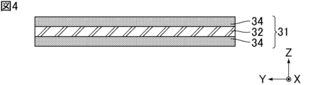
- FIG. 4 is a schematic cross-sectional view showing an example of the process of preparing the anode plate 31.
- FIG. 5 is a schematic cross-sectional view showing an example of the process of forming a dielectric layer.
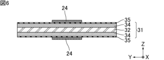
- FIG. 6 is a schematic cross-sectional view showing an example of the process of forming an insulating layer.
- FIG. 1 is a schematic perspective view showing an example of a capacitor array of the present invention.
- FIG. 2 is a schematic cross-sectional view showing an example of a cross section of a capacitor array including a
- FIG. 7 is a schematic cross-sectional view showing an example of the process of forming a solid electrolyte layer.
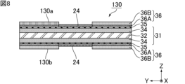
- FIG. 8 is a schematic cross-sectional view showing an example of the process of forming a conductor layer.
- FIG. 9 is a schematic plan view showing an example of a capacitor sheet.
- FIG. 10 is a schematic cross-sectional view showing how an example of the step of forming the first through groove is performed on a cross section along line segment a1-a2 in FIG.
- FIG. 11 is a schematic cross-sectional view showing how an example of the step of forming the first sealing layer is performed on the cross section shown in FIG. 10.
- FIG. 10 is a schematic cross-sectional view showing how an example of the step of forming the first through groove is performed on a cross section along line segment a1-a2 in FIG.
- FIG. 11 is a schematic cross-sectional view showing how an example of the step of forming the first sealing layer is performed on the cross section shown in FIG. 10.
- FIG. 12 is a schematic cross-sectional view showing how an example of the step of forming the second through groove is performed on a cross section along the line segment b1-b2 in FIG.
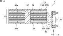
- FIG. 13 is a schematic cross-sectional view showing how an example of the step of forming the second sealing layer is performed on the cross section shown in FIG. 12.
- 14A, 14B, and 14C are schematic plan views showing an example of a capacitor sheet cutting process according to a comparative example outside the scope of the present invention.
- FIG. 15 is a schematic plan view showing an example of a capacitor array according to a comparative example.
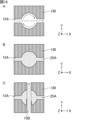
- 16A, 16B, and 16C are schematic plan views showing an example of a capacitor sheet cutting process according to Example 1 within the scope of the present invention.
- FIG. 17 is a schematic plan view showing an example of a capacitor array according to Example 1.
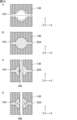
- 18A, FIG. 18B, FIG. 18C, and FIG. 18D are schematic plan views showing an example of a capacitor sheet cutting process according to Example 2 within the scope of the present invention.
- FIG. 19 is a schematic plan view showing an example of a capacitor array according to the second embodiment.
- FIG. 20 is a schematic plan view showing an example of an intersection area in the capacitor array according to Example 1.
- FIG. 21 is a schematic plan view from which the first sealing layer and the second sealing layer are removed from the capacitor array shown in FIG. 20.
- FIG. 22 is a schematic plan view showing a first modification of the intersection area in the capacitor array according to the first embodiment.
- FIG. 23 is a schematic plan view from which the first sealing layer and the second sealing layer are removed from the capacitor array shown in FIG. 22.
- FIG. 24 is a schematic plan view showing a second modification of the intersection area in the capacitor array according to the first embodiment.
- FIG. 25 is a schematic plan view showing a third modification of the intersection area in the capacitor array according to the first embodiment.
- FIG. 26 is a schematic plan view showing an example of an intersection area in a capacitor array according to Example 2.
- FIG. 27 is a schematic plan view showing a first modification of the intersection area in the capacitor array according to the second embodiment.
- FIG. 28 is a schematic plan view showing a second modification of the intersection area in the capacitor array according to the second embodiment.
- FIG. 29 is a schematic plan view showing a third modification of the intersection area in the capacitor array according to the second embodiment.
- FIG. 30 is a schematic plan view showing a fourth modification of the intersection area in the capacitor array according to the second embodiment.
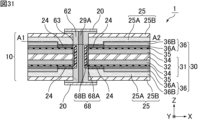
- FIG. 31 is a schematic cross-sectional view showing an example of a cross section of a capacitor array including a cross section along line segment A1-A2 in FIG.
- FIG. 32 is a schematic cross-sectional view showing an example of a cross section of a capacitor array including a cross section along line segment B1-B2 in FIG.
- the capacitor array of the present invention will be explained. Note that the present invention is not limited to the following configuration, and may be modified as appropriate without changing the gist of the present invention. Furthermore, the present invention also includes a combination of a plurality of individual preferred configurations described below.
- FIG. 1 is a schematic perspective view showing an example of a capacitor array of the present invention.
- the capacitor array 1 shown in FIG. 1 includes a capacitor layer 10. As shown in FIG. 1, the capacitor array 1 may further include a sealing layer 25 that seals the capacitor layer 10.
- the capacitor layer 10 includes a plurality of capacitor elements 30.
- the plurality of capacitor elements 30 are separated by a plurality of through grooves 15, and are arranged in a plane in a plane direction perpendicular to the thickness direction Z.
- the number of capacitor elements 30 included in the capacitor layer 10 is not particularly limited as long as it is two or more.
- the plurality of capacitor elements 30 may be arranged linearly, that is, along one direction (for example, the first direction They may be arranged along a direction (for example, a first direction X and a second direction Y). Further, the plurality of capacitor elements 30 may be arranged regularly or irregularly. The size, planar shape, etc. of the plurality of capacitor elements 30 may all be the same, or some or all of them may be different.
- the capacitor layer 10 may include two or more types of capacitor elements 30 having different areas.
- the capacitor layer 10 may include a capacitor element 30 whose planar shape is not rectangular.
- a rectangle means a square or a rectangle. Therefore, the capacitor layer 10 includes a capacitor element 30 whose planar shape is, for example, a quadrangle other than a rectangle, a polygon such as a triangle, a pentagon, or a hexagon, a shape including a curved part, a circle, an ellipse, etc. Good too.
- the capacitor layer 10 may include two or more types of capacitor elements 30 having different planar shapes.
- the capacitor layer 10 may or may not include a capacitor element 30 whose planar shape is rectangular.
- adjacent capacitor elements 30 are separated by a through groove 15. Adjacent capacitor elements 30 only need to be physically separated. Therefore, adjacent capacitor elements 30 may be electrically separated or may be electrically connected. For example, a set of capacitor elements 30 that are electrically separated and a set of capacitor elements 30 that are electrically connected may coexist.
- the through grooves 15 are preferably filled with an insulating material such as the sealing layer 25.
- Each of the capacitor elements 30 includes a first electrode layer, a second electrode layer, and a dielectric layer, and the first electrode layer and the second electrode layer face each other in the thickness direction Z with the dielectric layer interposed therebetween.
- FIG. 2 is a schematic cross-sectional view showing an example of a cross section of a capacitor array including a cross section along line segment a1-a2 in FIG. Note that the line segment a1-a2 in FIG. 2 corresponds to the line segment a1-a2 in FIG.
- FIG. 3 is a schematic cross-sectional view showing an example of a cross section of a capacitor array including a cross section along line b1-b2 in FIG. Note that the line segment b1-b2 in FIG. 3 corresponds to the line segment b1-b2 in FIG.
- the capacitor element 30 includes an anode plate 31, a cathode layer 36, and a dielectric layer 35. is facing. That is, the first electrode layer is the anode plate 31 and the second electrode layer is the cathode layer 36. Thereby, capacitor element 30 constitutes an electrolytic capacitor.
- the anode plate 31 has, for example, a core portion 32 made of metal, and a porous portion 34 provided on at least one main surface of the core portion 32.
- a dielectric layer 35 is provided on the surface of the porous portion 34, and a cathode layer 36 is provided on the surface of the dielectric layer 35.
- the cathode layer 36 includes, for example, a solid electrolyte layer 36A provided on the surface of the dielectric layer 35.
- the cathode layer 36 further includes a conductor layer 36B provided on the surface of the solid electrolyte layer 36A.
- capacitor element 30 constitutes a solid electrolytic capacitor.
- the core portion 32 is preferably made of a valve metal that exhibits a so-called valve action.
- Valve metals include, for example, simple metals such as aluminum, tantalum, niobium, titanium, and zirconium, and alloys containing at least one of these metals. Among these, aluminum or aluminum alloy is preferred.
- the porous portion 34 is provided on at least one main surface of the core portion 32. That is, the porous portion 34 may be provided on only one main surface of the core portion 32, or may be provided on both main surfaces of the core portion 32 as shown in FIGS. 2 and 3. . In this way, the anode plate 31 has the porous portion 34 on at least one main surface of the core portion 32.
- the porous portion 34 is preferably a porous layer formed on the surface of the core portion 32, and more preferably an etched layer.
- the shape of the anode plate 31 is preferably flat, and more preferably foil-like.
- plate-like also includes “foil-like”.
- the thickness of the anode plate 31 before etching treatment is preferably 60 ⁇ m or more and 200 ⁇ m or less.
- the thickness of the core portion 32 that is not etched after the etching process is preferably 15 ⁇ m or more and 70 ⁇ m or less.
- the thickness of the porous portion 34 is designed according to the required withstand voltage and capacitance, but it is preferable that the total thickness of the porous portions 34 on both sides of the core portion 32 is 10 ⁇ m or more and 180 ⁇ m or less.
- the pore diameter of the porous portion 34 is preferably 10 nm or more and 600 nm or less. Note that the pore diameter of the porous portion 34 means the median diameter D50 measured by a mercury porosimeter. The pore diameter of the porous portion 34 can be controlled, for example, by adjusting various etching conditions.
- the dielectric layer 35 is provided on the surface of the porous portion 34.
- the dielectric layer 35 is porous reflecting the surface condition of the porous portion 34, and has a finely uneven surface shape.
- the dielectric layer 35 is preferably made of an oxide film of the above-mentioned valve metal.
- an oxide film that becomes the dielectric layer 35 is formed by anodizing the anode plate 31 in an aqueous solution containing ammonium adipate (also called chemical conversion treatment). is formed. Since the dielectric layer 35 is formed along the surface of the porous portion 34, the dielectric layer 35 is provided with pores (recesses).
- the thickness of the dielectric layer 35 is designed according to the required withstand voltage and capacitance, but is preferably 10 nm or more and 100 nm or less.
- the cathode layer 36 is provided on the surface of the dielectric layer 35.
- examples of the constituent material of the solid electrolyte layer 36A include conductive polymers such as polypyrroles, polythiophenes, and polyanilines. Among these, polythiophenes are preferred, and poly(3,4-ethylenedioxythiophene) called PEDOT is particularly preferred. Further, the conductive polymer may contain a dopant such as polystyrene sulfonic acid (PSS).
- PSS polystyrene sulfonic acid
- the solid electrolyte layer 36A preferably includes an inner layer that fills the pores (recesses) of the dielectric layer 35 and an outer layer that covers the surface of the dielectric layer 35.
- the thickness of the solid electrolyte layer 36A from the surface of the porous portion 34 is preferably 2 ⁇ m or more and 20 ⁇ m or less.
- the solid electrolyte layer 36A is formed by forming a polymer film such as poly(3,4-ethylenedioxythiophene) on the surface of the dielectric layer 35 using a treatment liquid containing a monomer such as 3,4-ethylenedioxythiophene.
- the dielectric layer 35 may be formed by a method of forming the dielectric layer 35, or by a method of applying a dispersion of a polymer such as poly(3,4-ethylenedioxythiophene) to the surface of the dielectric layer 35 and drying it.
- the solid electrolyte layer 36A is formed in a predetermined area by applying the above treatment liquid or dispersion liquid to the surface of the dielectric layer 35 by a method such as sponge transfer, screen printing, dispenser coating, or inkjet printing. .
- the conductor layer 36B preferably includes at least one of a conductive resin layer and a metal layer. That is, the conductor layer 36B may include only a conductive resin layer, only a metal layer, or both a conductive resin layer and a metal layer.
- the conductive resin layer examples include a conductive adhesive layer containing at least one conductive filler selected from the group consisting of silver filler, copper filler, nickel filler, and carbon filler.
- the metal layer examples include metal plating films, metal foils, and the like.
- the metal layer is preferably made of at least one metal selected from the group consisting of nickel, copper, silver, and an alloy containing at least one of these metals as a main component.
- the main component means the elemental component having the largest weight ratio.
- the conductor layer 36B includes, for example, a carbon layer provided on the surface of the solid electrolyte layer 36A, and a copper layer provided on the surface of the carbon layer.
- the carbon layer is provided to electrically and mechanically connect the solid electrolyte layer 36A and the copper layer.
- the carbon layer is formed in a predetermined area by, for example, applying carbon paste to the surface of the solid electrolyte layer 36A by a method such as sponge transfer, screen printing, dispenser coating, or inkjet printing. Note that it is preferable to laminate the copper layer in the next step on the carbon layer in a viscous state before drying.
- the thickness of the carbon layer is preferably 2 ⁇ m or more and 20 ⁇ m or less.
- the copper layer is formed in a predetermined area by, for example, applying a copper paste to the surface of the carbon layer by a method such as sponge transfer, screen printing, spray coating, dispenser coating, or inkjet printing.
- the thickness of the copper layer is preferably 2 ⁇ m or more and 20 ⁇ m or less.
- the capacitor element 30 shown in FIGS. 2 and 3 has a first main surface 30a and a second main surface 30b that face each other in the thickness direction Z.
- the plurality of through grooves 15 include a first through groove 15A along the first direction X and a second through groove 15B along the second direction Y.
- the first direction X is perpendicular to the thickness direction Z.
- the second direction Y is perpendicular to the thickness direction Z and intersects with the first direction X.
- the first direction X and the second direction Y may be perpendicular to each other, as shown in FIG. 1, etc., or may intersect at an angle other than 90°.
- the width W1 of the first through groove 15A is (Here, the dimension in the second direction Y) is constant in the thickness direction Z.
- the first through groove 15A may have a taper in which the width W1 decreases from one of the first main surface 30a and the second main surface 30b of the capacitor element 30 toward the other.
- the width W1 of the first through groove 15A may become smaller from the first main surface 30a to the second main surface 30b of the capacitor element 30, or from the second main surface 30b of the capacitor element 30 to the first main surface 30b.
- the width W1 of the first through groove 15A may become smaller toward the surface 30a.
- the cross-sectional shape of the first through groove 15A along the thickness direction Z may be symmetrical or asymmetrical.
- the width W2 of the second through groove 15B is (Here, the dimension in the first direction X) is constant in the thickness direction Z.
- the second through groove 15B may have a taper in which the width W2 decreases from one of the first main surface 30a and the second main surface 30b of the capacitor element 30 toward the other.
- the width W2 of the second through groove 15B may become smaller from the first main surface 30a to the second main surface 30b of the capacitor element 30, or from the second main surface 30b of the capacitor element 30 to the first main surface 30b.
- the width W2 of the second through groove 15B may become smaller toward the surface 30a.
- the cross-sectional shape of the second through groove 15B along the thickness direction Z may be symmetrical or asymmetrical.
- the width W1 of the first through groove 15A becomes smaller from the first main surface 30a to the second main surface 30b of the capacitor element 30, and It is preferable that the width W2 of the second through groove 15B becomes smaller from the first main surface 30a to the second main surface 30b of the capacitor element 30.
- the taper angle of the first through groove 15A and the taper angle of the second through groove 15B are preferably different from each other.
- the taper angle of a through groove refers to the angle formed by two opposing sides forming the outline of the through groove when looking at a cross section along the thickness direction.
- the width W1 of the first through groove 15A becomes smaller from the first main surface 30a to the second main surface 30b of the capacitor element 30, and the width W1 of the first through groove 15A becomes smaller from the first main surface 30a to the second main surface 30b of the capacitor element 30.
- the taper angle of the second through groove 15B is preferably smaller than the taper angle of the first through groove 15A. In this case, since the inclination angle of the end face of the capacitor element 30 on the second through groove 15B side with respect to the thickness direction Z becomes smaller, the effective area of the capacitor element 30 can be increased on the second through groove 15B side.
- the maximum value of the width W2 of the second through groove 15B is preferably smaller than the maximum value of the width W1 of the first through groove 15A.
- the capacitor layer 10 among the regions where the capacitor element 30 does not exist, that is, the regions where the first through grooves 15A and the second through grooves 15B exist, at least the area where the second through grooves 15B exist can be made smaller. , it is possible to secure a large area in the capacitor layer 10 where the capacitor element 30 exists.
- the taper shape, taper angle, and width of the first through groove and the second through groove can be determined by observing the cross section along the thickness direction as shown in FIGS. 2 and 3 using a scanning electron microscope (SEM). It is confirmed.
- SEM scanning electron microscope
- the capacitor layer 10 has a dielectric layer 35 on which the cathode layer 36 is not provided on at least one of the first main surface 30a and the second main surface 30b of the capacitor element 30. It is preferable to further include an insulating layer 24 provided on the surface of. In this case, insulation between the anode plate 31 and the cathode layer 36 is ensured, and short circuits between the two are prevented.
- the insulating layer 24 may be provided on the surface of the dielectric layer 35 on the first main surface 30a side of the capacitor element 30, or may be provided on the surface of the dielectric layer 35 on the second main surface 30b side of the capacitor element 30. Alternatively, as shown in FIGS. 2 and 3, it may be provided on the surface of the dielectric layer 35 on both the first and second main surfaces 30a and 30b of the capacitor element 30. .
- the insulating layer 24 is made of an insulating material.
- the insulating layer 24 is preferably made of insulating resin.
- Examples of the insulating resin constituting the insulating layer 24 include polyphenylsulfone resin, polyethersulfone resin, cyanate ester resin, fluororesin (tetrafluoroethylene, tetrafluoroethylene/perfluoroalkyl vinyl ether copolymer, etc.), Examples include polyimide resins, polyamideimide resins, epoxy resins, and derivatives or precursors thereof.
- the insulating layer 24 may be made of the same resin as the sealing layer 25. Unlike the sealing layer 25, if the insulating layer 24 contains an inorganic filler, it may have an adverse effect on the capacitance effective portion of the capacitor element 30, so the insulating layer 24 is preferably made of a resin alone.
- the insulating layer 24 is formed by applying a mask material such as a composition containing an insulating resin to the surface of the porous portion 34 by a method such as sponge transfer, screen printing, dispenser coating, or inkjet printing. Formed in the area.
- a mask material such as a composition containing an insulating resin
- the insulating layer 24 may be formed on the porous portion 34 at a timing before the dielectric layer 35, or may be formed at a timing after the dielectric layer 35.
- the sealing layer 25 is provided on both main surfaces of the capacitor element 30 facing in the thickness direction Z, that is, on the first main surface 30a and the second main surface 30b of the capacitor element 30. It is provided.
- the sealing layer 25 is provided on both main surfaces of the capacitor element 30 facing in the thickness direction Z, that is, on the first main surface 30a and the second main surface 30b of the capacitor element 30. It is preferable to include the provided first sealing layer 25A.
- the first sealing layer 25A preferably extends within the first through groove 15A.
- the first sealing layer 25A does not extend into the second through groove 15B.
- the sealing layer 25 preferably further includes a second sealing layer 25B provided on the surface of the first sealing layer 25A.
- the second sealing layer 25B does not extend into the first through groove 15A.
- the second sealing layer 25B preferably extends within the second through groove 15B.
- the first sealing layer 25A extends within the first through groove 15A, and the second sealing layer 25B does not extend. preferable.
- the first sealing layer 25A does not extend into the second through groove 15B, and the second sealing layer 25B does. That is, as shown in FIG. 3, it is preferable that the first sealing layer 25A is separated by the second sealing layer 25B at a position overlapping the second through groove 15B in the thickness direction Z.
- the sealing layers 25 such as the first sealing layer 25A and the second sealing layer 25B are made of an insulating material.
- the sealing layer 25 is preferably made of insulating resin.
- Examples of the insulating resin constituting the sealing layer 25 include epoxy resin, phenol resin, and the like.
- the sealing layer 25 further contains a filler.
- Examples of the filler included in the sealing layer 25 include inorganic fillers such as silica particles and alumina particles.
- the constituent materials of the first sealing layer 25A and the second sealing layer 25B may be the same or different.
- the sealing layers 25 such as the first sealing layer 25A and the second sealing layer 25B are formed by, for example, a method of thermocompression bonding an insulating resin sheet, a method of applying an insulating resin paste and then thermosetting it, etc. It is formed to seal the capacitor layer 10.
- a layer such as a stress relaxation layer or a moisture-proof film may be provided between the capacitor layer 10 and the sealing layer 25.
- the capacitor array 1 having the cross section shown in FIGS. 2 and 3 is manufactured, for example, by the following method.
- FIG. 4 is a schematic cross-sectional view showing an example of the process of preparing the anode plate 31.
- an anode plate 31 having a porous portion 34 on at least one main surface of a core portion 32 is prepared.
- FIG. 5 is a schematic cross-sectional view showing an example of the process of forming a dielectric layer.
- a dielectric layer 35 is formed on the surface of the porous portion 34, as shown in FIG.
- a chemically formed foil may be prepared as the anode plate 31 in which the dielectric layer 35 is provided on the surface of the porous portion 34.
- FIG. 6 is a schematic cross-sectional view showing an example of the process of forming an insulating layer.
- an insulating resin is applied to the surface of the dielectric layer 35 by a method such as screen printing or dispenser coating. As shown, an insulating layer 24 is formed in a predetermined region.
- FIG. 7 is a schematic cross-sectional view showing an example of the process of forming a solid electrolyte layer.
- a solid electrolyte layer 36A is formed in a region of the surface of the dielectric layer 35 where the insulating layer 24 is not provided.
- the solid electrolyte layer 36A is formed by applying a dispersion of a polymer such as , 4-ethylenedioxythiophene) to the surface of the dielectric layer 35 and then drying it. Note that, after forming an inner layer that fills the pores (recesses) of the dielectric layer 35 as the solid electrolyte layer 36A, it is preferable to form an outer layer that covers the surface of the dielectric layer 35.
- FIG. 8 is a schematic cross-sectional view showing an example of the process of forming a conductor layer.
- a conductor layer 36B is formed on the surface of the solid electrolyte layer 36A.
- a carbon layer and a copper layer are sequentially formed from the solid electrolyte layer 36A side.
- a carbon layer is formed in a predetermined region by applying carbon paste to the surface of the solid electrolyte layer 36A by a method such as sponge transfer, screen printing, dispenser coating, or inkjet printing.
- a copper layer is formed in a predetermined area by applying a copper paste to the surface of the carbon layer by a method such as sponge transfer, screen printing, spray coating, dispenser coating, or inkjet printing.
- the cathode layer 36 including the solid electrolyte layer 36A and the conductor layer 36B is formed on the surface of the dielectric layer 35.
- FIG. 9 is a schematic plan view showing an example of a capacitor sheet.
- a capacitor sheet 130 including a cathode layer 24 and a cathode layer 36 is produced.
- the capacitor sheet 130 has a first main surface 130a and a second main surface 130b that face each other in the thickness direction Z.
- FIG. 10 is a schematic cross-sectional view showing how an example of the process of forming the first through groove is performed on a cross section along line segment a1-a2 in FIG.
- a first through groove 15A that penetrates the capacitor sheet 130 in the thickness direction Z is formed along the first direction X at a position that does not overlap with the cathode layer 36 in the thickness direction Z. .
- the first through groove 15A is formed by performing laser processing from the second main surface 130b side on the portion of the capacitor sheet 130 where the cross section along the line a1-a2 in FIG. 9 is formed. It's okay.
- the processing method for forming the first through groove 15A is not limited to laser processing, and may be, for example, a method such as dicing processing or router processing.
- the capacitor sheet 130 is cut along the first direction X.
- the capacitor sheet 130 can be prevented from being completely separated into a plurality of independent parts, thereby improving handling properties in subsequent processes.
- step of forming the first through groove 15A is not performed on the portion of the capacitor sheet 130 where the cross section along the line b1-b2 in FIG. 9 is formed.
- FIG. 11 is a schematic cross-sectional view showing how an example of the step of forming the first sealing layer is performed on the cross section shown in FIG. 10.
- an insulating resin sheet is thermocompression bonded to the capacitor sheet 130 having the cross section shown in FIG.
- the first sealing layer 25A is formed on the first main surface 130a and the second main surface 130b of the capacitor sheet 130, and is filled in the first through groove 15A.
- the capacitor sheet 130 is fixed by the first sealing layer 25A while being partially separated by the first through groove 15A.
- the first sealing layer 25A formed in this way is provided on the first main surface 130a and the second main surface 130b of the capacitor sheet 130, as shown in FIG. 11, and is provided in the first through groove 15A. Extending.
- the first sealing layer 25A When forming the first sealing layer 25A, as described above, in the case where the capacitor sheet 130 is provided with the first through groove 15A, but is not completely separated and does not have multiple independent parts. In this case, the portions of the capacitor sheet 130 that are separated by the first through groove 15A move and come into contact with each other due to the flow of the constituent material (for example, resin material) of the first sealing layer 25A. Malfunctions can be prevented. Therefore, it is possible to prevent short circuits between capacitor elements in the capacitor array obtained later.
- the constituent material for example, resin material
- the above-mentioned problems can be prevented even if the press processing is performed at high pressure. Therefore, a large processing margin can be ensured when forming the first sealing layer 25A, resulting in improved processability. If the first sealing layer 25A can be formed by high-pressure press working, the adhesion between the first sealing layer 25A and the capacitor sheet 130 can be improved, and voids in the first sealing layer 25A can be reduced. This leads to improved reliability of the capacitor array obtained later.
- FIG. 12 is a schematic cross-sectional view showing how an example of the step of forming the second through groove is performed on a cross section along the line segment b1-b2 in FIG.
- a portion of the capacitor sheet 130 provided with the first sealing layer 25A, where a cross section along the line b1-b2 in FIG. 9 is formed, is subjected to laser processing, for example, from the first main surface 130a side.
- the second through groove 15B that penetrates the capacitor sheet 130 and the first sealing layer 25A in the thickness direction Z is formed at a position that does not overlap with the cathode layer 36 in the thickness direction Z. It is formed along the direction Y.
- the second through groove 15B may be formed.
- the processing method for forming the second through groove 15B is not limited to laser processing, and may be, for example, dicing processing, router processing, or the like.
- the processing method for forming the second through groove 15B may be the same as the processing method for forming the first through groove 15A, or may be different.
- the capacitor sheet 130 and the first sealing layer 25A are , are cut all at once along the second direction Y.
- the second through groove 15B is cut along the second direction Y so that the capacitor sheet 130 provided with the first sealing layer 25A is not cut continuously from one end to the other end along the second direction Y. It is preferable to form. This can prevent the capacitor sheet 130 on which the first sealing layer 25A is provided from being completely separated into a plurality of independent parts, thereby improving handling properties in subsequent steps.
- step of forming the second through groove 15B is not performed on the portion of the capacitor sheet 130 where the cross section along the line a1-a2 in FIG. 9 is formed.
- FIG. 13 is a schematic cross-sectional view showing how an example of the step of forming the second sealing layer is performed on the cross section shown in FIG. 12.
- the second sealing layer 25B is formed on the surface of the first sealing layer 25A, as shown in FIG. While being formed, the second through groove 15B is filled.
- the second sealing layer 25B formed in this way is provided on the surface of the first sealing layer 25A, as shown in FIG. 13, and extends into the second through groove 15B.
- the capacitor layer 10 in a planar arrangement is fabricated by being divided into a plurality of capacitor elements 30 by the first through groove 15A and the second through groove 15B, and the plurality of capacitor elements 30 are divided into a plurality of capacitor elements 30 in the first sealing layer. 25A and the second sealing layer 25B.
- a capacitor array 1 having a cross section shown in FIGS. 2 and 3 is manufactured.
- the cutting step for dividing the capacitor sheet 130 into a plurality of capacitor elements 30 is divided into a step of forming the first through groove 15A and a step of forming the second through groove 15B. Furthermore, a step of forming the first sealing layer 25A is performed between these steps. This makes it possible to prevent the capacitor sheet 130 from being completely separated into a plurality of independent parts during the manufacturing process, thereby improving handling properties. Furthermore, in the step of forming the first sealing layer 25A, press working can be performed at high pressure, which improves workability and also leads to improved reliability of the capacitor array 1.
- FIGS. 14A, 14B, and 14C are schematic plan views showing an example of a capacitor sheet cutting process according to a comparative example outside the scope of the present invention.
- FIG. 15 is a schematic plan view showing an example of a capacitor array according to a comparative example.
- the first sealing layer 25A is filled in the first through groove 15A as shown in FIG. 14B.
- metal scraps for example, aluminum scraps
- FIG. 14C when forming the second through groove 15B to intersect with the first through groove 15A, metal scraps (for example, aluminum scraps) generated by cutting the capacitor sheet 130 are spread between the first through groove 15A and the second through groove 15B. If it is attached so as to straddle the area where it intersects with the through groove 15B, there is a risk that a short circuit will occur between adjacent capacitor elements 30 (see FIG. 15) in the finished product. In FIG. 14C, locations where short circuits occur are shown surrounded by broken lines.
- FIGS. 16A, 16B, and 16C are schematic plan views showing an example of a capacitor sheet cutting process according to Example 1 within the scope of the present invention.
- FIG. 17 is a schematic plan view showing an example of a capacitor array according to Example 1.
- the first through groove 15A when forming the first through groove 15A, the first through groove 15A is formed so that the area of the portion intersecting with the second through groove 15B is increased.
- the planar shape at this time is not limited to a circle.
- FIG. 16B after filling the first sealing layer 25A into the first through groove 15A, as shown in FIG. 16C, when forming the second through groove 15B, metal scraps (for example, aluminum Even if dust) is generated, the width of the first through groove 15A is wide in the area where the first through groove 15A intersects with the second through groove 15B, so that short circuits will not occur between adjacent capacitor elements 30 (see FIG. 17) in the finished product. The risk of defects occurring can be reduced.
- the capacitor element 30 A large effective area can be secured.
- cross section of the capacitor array including the cross section along line segment a1-a2 in FIG. 17 corresponds to FIG. 2
- the cross section of the capacitor array including the cross section along line segment b1-b2 in FIG. 17 corresponds to FIG. do.
- FIGS. 18A, 18B, 18C, and 18D are schematic plan views showing an example of a capacitor sheet cutting process according to Example 2 within the scope of the present invention.
- FIG. 19 is a schematic plan view showing an example of a capacitor array according to the second embodiment.
- the first through groove 15A is After filling the first sealing layer 25A into the first through groove 15A, as shown in FIG. 18C, when forming the second through groove 15B, the gap between adjacent capacitor elements 30 (see FIG. 19) in the finished product is A short circuit may occur.
- FIG. 18C locations where short circuits occur are shown surrounded by broken lines.
- a method such as laser machining may be used to cut the short-circuited portion in the intersection area of the first through groove 15A and the second through groove 15B again.
- the planar shape upon cutting is not limited to a linear shape.
- the cutting direction is not limited to the first direction X.
- the cutting shown in FIG. 18D can further reduce the risk of a short circuit occurring between adjacent capacitor elements 30 (see FIG. 19) in the finished product. As shown in FIG. 18D, as long as at least the shorted portion is cut, other portions may be cut.
- the processing area for cutting the short circuit again should be smaller than the area of the first through groove 15A in the intersection area of the first through groove 15A and the second through groove 15B. is preferred.
- FIG. 20 is a schematic plan view showing an example of an intersection area in the capacitor array according to Example 1.
- FIG. 21 is a schematic plan view from which the first sealing layer and the second sealing layer are removed from the capacitor array shown in FIG. 20.
- the first through groove 15A and the second through groove 15B are orthogonal to each other.
- the first virtual groove 115A extends the first penetration groove 15A to the intersection region I.
- the intersection points (four points in FIG. 21) between the second through groove 15B and the second virtual groove 115B extending to the intersection area I are located inside the intersection area I (circle in FIG. 21).
- the area of the intersection region I is the area where the first virtual groove 115A and the second virtual groove 115B overlap (the area 4 in FIG. 21). larger than the area of the rectangle (enclosed by two points).
- Example 1 since the width of the first through groove 15A in the intersection region I is wide, the risk of short circuit failure occurring between adjacent capacitor elements 30 can be reduced.
- the area of the intersection region I is large, the area of the portion that functions as a support that connects the front and back sealing layers becomes large, so the adhesion strength between the front and back surfaces becomes high. As a result, delamination can be suppressed.
- intersection area I when the first sealing layer 25A and the second sealing layer 25B extend also within the intersection area I, when the intersection area I is viewed from the thickness direction Z, the intersection area I
- the second sealing layer 25B is located inside the first sealing layer 25A, and the area of the second sealing layer 25B in the intersection area I is the second virtual groove 115B in the intersection area I (see FIG. (see 21).
- At least one of the corners between the first through groove 15A and the intersection region I has a curved surface (so-called R surface) or an obtuse angle surface.
- R surface curved surface
- obtuse angle surface the stress concentrated at the corners in the intersection region I is relaxed, so cracks and delamination can be suppressed.
- all of the corners between the first through groove 15A and the intersection region I have a curved surface or an obtuse angle surface.
- a corner portion and a corner portion having an obtuse angle surface may coexist.
- At least one of the corners between the second penetration groove 15B and the intersection area I has a curved surface or an obtuse angle surface, and all the corners between the second penetration groove 15B and the intersection area I have a curved surface or an obtuse angle surface. It is more preferable to have an obtuse angle surface.
- two or more corners have a curved surface or an obtuse surface, only the corner having the curved surface may exist, only the corner having the obtuse surface may exist, or the corner having the curved surface may exist.
- a corner portion and a corner portion having an obtuse angle surface may coexist.
- At least one corner between the first through groove 15A and the intersection area I has a curved surface or an obtuse angle surface
- at least one corner between the second through groove 15B and the intersection area I has a curved surface or an obtuse angle surface
- all corners between the first through groove 15A and the intersection area I have a curved surface or an obtuse angle surface
- all corners between the second through groove 15B and the intersection area I have an obtuse angle surface.
- FIG. 22 is a schematic plan view showing a first modification of the intersection area in the capacitor array according to Example 1.
- FIG. 23 is a schematic plan view from which the first sealing layer and the second sealing layer are removed from the capacitor array shown in FIG. 22.
- first through groove 15A and the second through groove 15B may not be perpendicular to each other but may intersect at an angle other than 90°.
- the first virtual groove 115A extends the first penetration groove 15A to the intersection region I.
- the intersection points (four points in FIG. 23) between the second through groove 15B and the second virtual groove 115B extending to the intersection area I are located inside the intersection area I (circle in FIG. 23).
- FIG. 24 is a schematic plan view showing a second modification of the intersection area in the capacitor array according to Example 1.
- the planar shape of the intersection region I when viewed from the thickness direction Z may be a polygon such as a quadrangle.
- the planar shape of the intersection region I when viewed from the thickness direction Z is not particularly limited, and may be, for example, a rectangle (square or rectangle), a quadrilateral other than a rectangle, a polygon such as a triangle, pentagon, or hexagon, a circle, or an ellipse. , a shape that is a combination of these, etc.
- FIG. 25 is a schematic plan view showing a third modification of the intersection area in the capacitor array according to Example 1.
- the corner between the first through groove 15A and the intersection region I does not have to have a curved surface or an obtuse surface.
- the corner between the second through groove 15B and the intersection region I does not need to have a curved surface or an obtuse angle surface.
- FIG. 26 is a schematic plan view showing an example of a crossing area in a capacitor array according to Example 2.
- intersection area I when the first sealing layer 25A and the second sealing layer 25B extend also within the intersection area I, when the intersection area I is viewed from the thickness direction Z, the intersection area I
- the second sealing layer 25B is located inside the first sealing layer 25A, and the area of the second sealing layer 25B in the intersection area I is the second virtual groove 115B in the intersection area I (see FIG. (see 21).
- the other configurations are the same as in the first embodiment.
- the second sealing layer 25B has a linear portion within the intersection region I along the first through groove 15A.
- the linear portion of the second sealing layer 25B may exist in both the positive direction and the negative direction of the first direction X, or may exist only in either one.
- At least one of the corners between the first through groove 15A and the intersection area I has a curved surface or an obtuse angle surface, and the corner between the first through groove 15A and the intersection area I More preferably, all of the curved surfaces or obtuse-angled surfaces have curved surfaces or obtuse angle surfaces.
- all of the curved surfaces or obtuse-angled surfaces have curved surfaces or obtuse angle surfaces.
- At least one of the corners between the second penetration groove 15B and the intersection area I has a curved surface or an obtuse angle surface, and all the corners between the second penetration groove 15B and the intersection area I have a curved surface or an obtuse angle surface. It is more preferable to have an obtuse angle surface.
- two or more corners have a curved surface or an obtuse surface, only the corner having the curved surface may exist, only the corner having the obtuse surface may exist, or the corner having the curved surface may exist.
- a corner portion and a corner portion having an obtuse angle surface may coexist.
- At least one corner between the first through groove 15A and the intersection area I has a curved surface or an obtuse angle surface
- at least one corner between the second through groove 15B and the intersection area I has a curved surface or an obtuse angle surface
- all corners between the first through groove 15A and the intersection area I have a curved surface or an obtuse angle surface
- all corners between the second through groove 15B and the intersection area I have an obtuse angle surface.
- first through groove 15A and the second through groove 15B are perpendicular to each other, but the first through groove 15A and the second through groove 15B are not perpendicular to each other and form an angle other than 90°. They may also intersect.
- FIG. 27 is a schematic plan view showing a first modification of the intersection area in the capacitor array according to the second embodiment.
- the second sealing layer 25B may have a circular portion or an elliptical portion within the intersection region I.
- FIG. 28 is a schematic plan view showing a second modification of the intersection area in the capacitor array according to the second embodiment.
- the planar shape of the intersection region I when viewed from the thickness direction Z may be a polygon such as a quadrangle.
- the second sealing layer 25B has a polygonal part such as a quadrangle in the intersection area I, but it may also have a linear part, or a circular part or an elliptical part. May have.
- FIG. 29 is a schematic plan view showing a third modification of the intersection area in the capacitor array according to the second embodiment.
- the corner between the first through groove 15A and the intersection region I does not have to have a curved surface or an obtuse surface.
- the corner between the second through groove 15B and the intersection region I does not need to have a curved surface or an obtuse angle surface.
- the second sealing layer 25B has a linear part in the intersection area I, but it may also have a polygonal part such as a quadrangle, or a circular part or an elliptical part. May have.
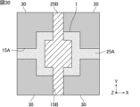
- FIG. 30 is a schematic plan view showing a fourth modification of the intersection area in the capacitor array according to the second embodiment.
- the width of the linear portion of the second sealing layer 25B may be wider than the width of the first through groove 15A.
- the capacitor array 1 shown in FIG. 1 further includes a through-hole conductor 60.
- the through-hole conductor 60 includes a first through-hole conductor 62 that is electrically connected to the first electrode layer (for example, the anode plate 31) of the capacitor element 30, and a second electrode layer (for example, the cathode layer 36) of the capacitor element 30. It is preferable that at least one of the second through-hole conductors 64 electrically connected to the second through-hole conductor 64 be included.
- the through-hole conductor 60 more specifically, the first through-hole conductor 62 and the second through-hole conductor 64 are each provided to penetrate the capacitor element 30 in the thickness direction Z of the capacitor layer 10. is preferred.
- the anode plate 31 and cathode layer 36 of the capacitor element 30 are led out using the first through-hole conductor 62 and the second through-hole conductor 64, respectively.
- FIG. 31 is a schematic cross-sectional view showing an example of a cross section of a capacitor array including a cross section along line segment A1-A2 in FIG. Note that the line segment A1-A2 in FIG. 31 corresponds to the line segment A1-A2 in FIG.
- the first through-hole conductor 62 is preferably provided so as to penetrate the capacitor element 30 in the thickness direction Z of the capacitor layer 10. More specifically, the first through-hole conductor 62 is preferably provided at least on the inner wall surface of the first through-hole 63 that penetrates the capacitor element 30 in the thickness direction Z.
- the first through-hole conductor 62 is electrically connected to the end surface of the anode plate 31 that faces the inner wall surface of the first through-hole 63 in a plane direction perpendicular to the thickness direction Z.
- the plane direction is a direction that includes the first direction X and the second direction Y that are perpendicular to the thickness direction Z.
- the core portion 32 and the porous portion 34 be exposed on the end face of the anode plate 31 that is electrically connected to the first through-hole conductor 62.
- the porous portion 34 is also electrically connected to the first through-hole conductor 62.
- the first through-hole conductor 62 is formed, for example, as follows. First, the first through-hole 63 is formed by performing drilling, laser processing, etc. on a portion where the first through-hole conductor 62 is to be formed. Then, the first through-hole conductor 62 is formed by metallizing the inner wall surface of the first through-hole 63 with a low-resistance metal such as copper, gold, or silver. When forming the first through-hole conductor 62, processing is facilitated by, for example, metalizing the inner wall surface of the first through-hole 63 by electroless copper plating, electrolytic copper plating, or the like.
- the method of forming the first through-hole conductor 62 in addition to the method of metalizing the inner wall surface of the first through-hole 63, there is a method of filling the first through-hole 63 with metal, a composite material of metal and resin, etc. It may be.
- the capacitor array 1 preferably further includes an anode connection layer 68 provided between the first through-hole conductor 62 and the end surface of the anode plate 31.
- the anode connection layer 68 is in contact with both the first through-hole conductor 62 and the end surface of the anode plate 31.
- the anode connection layer 68 Since the anode connection layer 68 is provided between the first through-hole conductor 62 and the end surface of the anode plate 31, the anode connection layer 68 serves as a barrier layer for the anode plate 31, more specifically, as a barrier layer for the anode plate 31. and functions as a barrier layer for the porous portion 34.
- the anode connection layer 68 By using such an anode connection layer 68, dissolution of the anode plate 31 that occurs during chemical treatment for forming the conductive portion 20, etc., which will be described later, is suppressed, and in turn, infiltration of the chemical liquid into the capacitor element 30 is suppressed. Therefore, the reliability of the capacitor array 1 can be easily improved.
- the first through-hole conductor 62 and the end surface of the anode plate 31 are preferably electrically connected via an anode connection layer 68.
- the anode connection layer 68 may include, in order from the end surface side of the anode plate 31, a first anode connection layer 68A and a second anode connection layer 68B.
- the first anode connection layer 68A may be a layer containing zinc as a main component
- the second anode connection layer 68B may be a layer containing nickel or copper as a main component.
- the first anode connection layer 68A is formed on the end face of the anode plate 31 by, for example, displacing and precipitating zinc by zincate treatment
- the second anode connection layer 68B is formed by, for example, electroless nickel plating or It is formed on the surface of the first anode connection layer 68A by electroless copper plating.
- the first anode connection layer 68A may disappear when forming the second anode connection layer 68B, and in this case, the anode connection layer 68 may be composed only of the second anode connection layer 68B.
- the anode connection layer 68 includes a layer containing nickel as a main component. In this case, since damage to the metal (for example, aluminum) constituting the anode plate 31 is reduced, the barrier properties of the anode connection layer 68 with respect to the anode plate 31 are easily improved.
- the dimensions of the anode connection layer 68 are preferably larger than the dimensions of the anode plate 31 in the thickness direction Z. In this case, since the entire end surface of the anode plate 31 is covered with the anode connection layer 68, the barrier properties of the anode connection layer 68 against the anode plate 31 are likely to be improved.
- the dimensions of the anode connection layer 68 are preferably larger than 100% and 200% or less of the dimensions of the anode plate 31.
- the dimensions of the anode connection layer 68 may be the same as the dimensions of the anode plate 31 or may be smaller than the dimensions of the anode plate 31.
- the anode connection layer 68 may not be provided between the first through-hole conductor 62 and the end surface of the anode plate 31.
- the first through-hole conductor 62 may be directly connected to the end surface of the anode plate 31.
- the first through-hole conductor 62 when viewed from the thickness direction Z, is electrically connected to the end surface of the anode plate 31 over the entire circumference of the first through-hole 63. is preferred.
- an anode connection layer 68 when an anode connection layer 68 is provided between the first through-hole conductor 62 and the end surface of the anode plate 31, when viewed from the thickness direction Z, the first through-hole conductor 62 is , it is preferable that the entire circumference of the first through hole 63 be connected to the anode connection layer 68 .
- the contact area between the first through-hole conductor 62 and the anode connection layer 68 becomes large, the connection resistance between the first through-hole conductor 62 and the anode connection layer 68 is easily reduced. As a result, the connection resistance between the first through-hole conductor 62 and the anode plate 31 can be easily reduced, so that the equivalent series resistance (ESR) of the capacitor element 30 can be easily reduced. Furthermore, since the adhesion between the first through-hole conductor 62 and the anode connection layer 68 is easily improved, problems such as peeling between the first through-hole conductor 62 and the anode connection layer 68 due to thermal stress may occur. It becomes difficult.
- the capacitor array 1 preferably further includes a conductive part 20 electrically connected to the first through-hole conductor 62.
- the conductive portion 20 is provided on the surface of the first through-hole conductor 62.
- the conductive portion 20 can function as a connection terminal of the capacitor array 1 (capacitor element 30).
- the constituent material of the conductive part 20 examples include low-resistance metals such as silver, gold, and copper.
- the conductive portion 20 is formed, for example, by plating the surface of the first through-hole conductor 62.
- the adhesion between the conductive part 20 and the first through-hole conductor 62 may be used.
- a mixed material of resin and at least one conductive filler selected from the group consisting of copper filler, nickel filler, and carbon filler may be used.
- the capacitor array 1 further includes a first resin filling portion 29A in which the first through hole 63 is filled with a resin material.
- the first resin filling portion 29A is provided in a space surrounded by the first through-hole conductor 62 on the inner wall surface of the first through-hole 63.
- the coefficient of thermal expansion of the first resin filled portion 29A is preferably larger than the coefficient of thermal expansion of the first through-hole conductor 62. More specifically, the coefficient of thermal expansion of the resin material filled in the first through-hole 63 is preferably larger than the coefficient of thermal expansion of the constituent material (for example, copper) of the first through-hole conductor 62.
- the first resin filling portion 29A more specifically, the resin material filled in the first through hole 63 expands in a high temperature environment, so that the first through hole conductor 62 fills the first through hole 63. Since the first through-hole conductor 62 is pressed against the inner wall surface of the first through-hole 63 from the inside to the outside, the occurrence of delamination of the first through-hole conductor 62 is sufficiently suppressed.
- the coefficient of thermal expansion of the first resin filling portion 29A may be the same as the coefficient of thermal expansion of the first through-hole conductor 62, or may be smaller than the coefficient of thermal expansion of the first through-hole conductor 62. More specifically, the coefficient of thermal expansion of the resin material filled in the first through-hole 63 may be the same as the coefficient of thermal expansion of the constituent material of the first through-hole conductor 62, or The coefficient of thermal expansion may be smaller than that of the constituent material of No. 62.
- the capacitor array 1 does not need to include the first resin filling part 29A.
- the first through-hole conductor 62 is provided not only on the inner wall surface of the first through-hole 63 but also throughout the inside of the first through-hole 63.
- FIG. 32 is a schematic cross-sectional view showing an example of a cross section of a capacitor array including a cross section along line segment B1-B2 in FIG. Note that the line segment B1-B2 in FIG. 32 corresponds to the line segment B1-B2 in FIG.
- the second through-hole conductor 64 is preferably provided so as to penetrate the capacitor element 30 in the thickness direction Z of the capacitor layer 10. More specifically, the second through-hole conductor 64 is formed on at least the inner wall surface of a second through-hole 65 that penetrates in the thickness direction Z through the capacitor element 30 in which the first through-hole conductor 62 shown in FIG. 31 etc. is provided. It is preferable that it is provided.
- the second through-hole conductor 64 is preferably electrically connected to the cathode layer 36.
- the conductive portion 40 is provided on the surface of the second through-hole conductor 64, and can function as a connection terminal of the capacitor array 1 (capacitor element 30).
- the via conductor 42 is provided so as to penetrate the sealing layer 25 in the thickness direction Z and be connected to the conductive part 40 and the cathode layer 36. Therefore, in the example shown in FIG. 32, the second through-hole conductor 64 is electrically connected to the cathode layer 36 via the conductive portion 40 and the via conductor 42. In this case, the capacitor array 1 can be made smaller.
- the second through-hole conductor 64 is formed, for example, as follows. First, a through hole is formed by performing drilling, laser processing, etc. on a portion where the second through hole conductor 64 is to be formed. Next, an insulating layer is formed by filling the formed through-hole with a constituent material (for example, a resin material) of the second sealing layer 25B. Then, the second through hole 65 is formed by performing drilling, laser processing, etc. on the formed insulating layer. At this time, by making the diameter of the second through hole 65 smaller than the diameter of the insulating layer, the constituent material of the second sealing layer 25B is placed between the previously formed through hole and the second through hole 65. make it exist.
- a through hole is formed by performing drilling, laser processing, etc. on a portion where the second through hole conductor 64 is to be formed.
- an insulating layer is formed by filling the formed through-hole with a constituent material (for example, a resin material) of the second sealing layer 25B.
- the second through hole 65 is formed by
- the second through-hole conductor 64 is formed by metallizing the inner wall surface of the second through-hole 65 with a low-resistance metal such as copper, gold, or silver.
- a low-resistance metal such as copper, gold, or silver.
- processing is facilitated by, for example, metalizing the inner wall surface of the second through-hole 65 by electroless copper plating, electrolytic copper plating, or the like.
- the method of forming the second through-hole conductor 64 in addition to the method of metalizing the inner wall surface of the second through-hole 65, there is a method of filling the second through-hole 65 with metal, a composite material of metal and resin, etc. It may be.
- Examples of the constituent material of the conductive part 40 include low-resistance metals such as silver, gold, and copper.
- the conductive portion 40 is formed, for example, by plating the surface of the second through-hole conductor 64.
- the adhesion between the conductive part 40 and the second through-hole conductor 64 may be used.
- a mixed material of resin and at least one conductive filler selected from the group consisting of copper filler, nickel filler, and carbon filler may be used.
- the constituent material of the via conductor 42 for example, the same material as the constituent material of the conductive part 40 can be mentioned.
- the via conductor 42 may be formed by plating the inner wall surface of a through hole provided to penetrate the sealing layer 25 in the thickness direction Z, or by performing heat treatment after filling with a conductive paste. It is formed by
- the capacitor array 1 further includes a second resin filling part 29B in which the second through hole 65 is filled with a resin material, as shown in FIGS. 1 and 32.
- the second resin filling portion 29B is provided in a space surrounded by the second through-hole conductor 64 on the inner wall surface of the second through-hole 65.
- the coefficient of thermal expansion of the second resin filling portion 29B is preferably larger than the coefficient of thermal expansion of the second through-hole conductor 64. More specifically, the coefficient of thermal expansion of the resin material filled in the second through-hole 65 is preferably larger than the coefficient of thermal expansion of the constituent material (for example, copper) of the second through-hole conductor 64.
- the second resin filling portion 29B more specifically, the resin material filled in the second through hole 65 expands in a high temperature environment, so that the second through hole conductor 64 fills the second through hole 65. Since it is pressed against the inner wall surface of the second through hole 65 from the inside to the outside, the occurrence of delamination of the second through hole conductor 64 is sufficiently suppressed.
- the coefficient of thermal expansion of the second resin filled portion 29B may be the same as the coefficient of thermal expansion of the second through-hole conductor 64, or may be smaller than the coefficient of thermal expansion of the second through-hole conductor 64. More specifically, the coefficient of thermal expansion of the resin material filled in the second through-hole 65 may be the same as the coefficient of thermal expansion of the constituent material of the second through-hole conductor 64, or The coefficient of thermal expansion may be smaller than that of the constituent material of No. 64.
- the capacitor array 1 does not need to include the second resin filling part 29B.
- the second through-hole conductor 64 is preferably provided not only on the inner wall surface of the second through-hole 65 but also throughout the inside of the second through-hole 65.
- the second sealing layer 25B preferably extends between the anode plate 31 and the second through-hole conductor 64.
- the second sealing layer 25B is in contact with both the anode plate 31 and the second through-hole conductor 64.
- the second sealing layer 25B extends between the anode plate 31 and the second through-hole conductor 64, as shown in FIG. , it is preferable that the core portion 32 and the porous portion 34 are exposed. In this case, the contact area between the second sealing layer 25B and the porous portion 34 is increased, which improves the adhesion between them, so that separation between the second sealing layer 25B and the porous portion 34, etc. Problems are less likely to occur.
- the constituent material of the insulating layer 24 enters the pores of the porous part 34, and the porous part 34 becomes porous.
- an insulating layer 24 extending inside the portion 34 is provided around the second through-hole conductor 64 .
- the insulation between the anode plate 31 and the second through-hole conductor 64 and, in turn, the insulation between the anode plate 31 and the cathode layer 36 are sufficiently ensured, and short circuits between the two are sufficiently prevented.
- the constituent material of the second sealing layer 25B enters the pores of the porous portion 34.
- the mechanical strength of the porous portion 34 is improved, and the occurrence of delamination due to pores in the porous portion 34 is suppressed.
- the coefficient of thermal expansion of the second sealing layer 25B is preferably larger than the coefficient of thermal expansion of the second through-hole conductor 64. More specifically, the coefficient of thermal expansion of the constituent material of the second sealing layer 25B is preferably larger than the coefficient of thermal expansion of the constituent material (for example, copper) of the second through-hole conductor 64. In this case, the second sealing layer 25B, more specifically, the constituent material of the second sealing layer 25B expands in a high-temperature environment, thereby pressing the porous portion 34 and the second through-hole conductor 64. , the occurrence of delamination is sufficiently suppressed.
- the coefficient of thermal expansion of the second sealing layer 25B may be the same as the coefficient of thermal expansion of the second through-hole conductor 64, or may be smaller than the coefficient of thermal expansion of the second through-hole conductor 64. More specifically, the coefficient of thermal expansion of the constituent material of the second sealing layer 25B may be the same as the coefficient of thermal expansion of the constituent material of the second through-hole conductor 64, or may be the same as that of the constituent material of the second through-hole conductor 64. It may be smaller than the coefficient of thermal expansion of the constituent materials.
- the through-hole conductor 60 includes a third electrode layer that is not electrically connected to the first electrode layer (for example, the anode plate 31) and the second electrode layer (for example, the cathode layer 36) of the capacitor element 30. It may also include through-hole conductors.
- the first imaginary groove that extends the first through groove to the intersection area and the second through groove are formed.
- the embodiment is not limited to the above embodiment as long as the intersection with the second virtual groove extending to the intersection area is located inside the intersection area. Therefore, various applications and modifications can be made within the scope of the present invention regarding the configuration, manufacturing conditions, etc. of the capacitor array.
- the capacitor elements are not limited to electrolytic capacitors such as solid electrolytic capacitors.
- the capacitor elements are, for example, ceramic capacitors using barium titanate, thin film capacitors using silicon nitride (SiN), silicon dioxide (SiO 2 ), hydrogen fluoride (HF), etc., MIM ( A trench type capacitor or the like having a metal insulator structure may also be configured.
- the capacitor element is a capacitor based on a metal such as aluminum. It is preferable to configure an electrolytic capacitor, and more preferably to configure an electrolytic capacitor based on a metal such as aluminum.
- the capacitor array of the present invention is used, for example, in composite electronic components.
- a composite electronic component includes, for example, the capacitor array of the present invention and an electronic component electrically connected to the external electrode layer of the capacitor array of the present invention.
- the electronic component electrically connected to the external electrode layer may be a passive element, an active element, or both a passive element and an active element. , a composite of a passive element and an active element.
- passive elements examples include inductors and the like.
- Active elements include memory, GPU (Graphical Processing Unit), CPU (Central Processing Unit), MPU (Micro Processing Unit), PMIC (Power Management IC), etc.
- the capacitor array of the present invention When the capacitor array of the present invention is used in a composite electronic component, the capacitor array of the present invention is treated as a substrate on which the electronic component is mounted, for example. Therefore, by making the capacitor array of the present invention into a sheet shape as a whole, and furthermore, by making the electronic components mounted on the capacitor array of the present invention into a sheet shape, it is possible to connect the electronic components through through-hole conductors that penetrate the electronic components in the thickness direction. , it becomes possible to electrically connect the capacitor array of the present invention and electronic components in the thickness direction. As a result, it becomes possible to configure passive elements and active elements as electronic components like a collective module.
- a switching regulator can be formed by electrically connecting the capacitor array of the present invention between a voltage regulator including a semiconductor active element and a load to which the converted DC voltage is supplied.
- a circuit layer is formed on one main surface of a capacitor matrix sheet on which a plurality of capacitor arrays of the present invention are laid out, and then the circuit layer is electrically connected to a passive element or an active element as an electronic component. You can also connect directly.
- the capacitor array of the present invention may be placed in a cavity provided in advance on a substrate, filled with resin, and then a circuit layer may be formed on the resin.
- a passive element or an active element as another electronic component may be mounted in another cavity portion of the same substrate.
- the capacitor array of the present invention may be mounted on a smooth carrier such as a wafer or glass, an outer layer made of resin may be formed, a circuit layer may be formed, and the circuit layer may be used as a passive element or an active element as an electronic component. It may be electrically connected to the element.
- a smooth carrier such as a wafer or glass
- an outer layer made of resin may be formed
- a circuit layer may be formed, and the circuit layer may be used as a passive element or an active element as an electronic component. It may be electrically connected to the element.
- a capacitor layer including a plurality of capacitor elements arranged in a plane in a plane perpendicular to the thickness direction by being divided by a plurality of through grooves,
- Each of the capacitor elements includes a first electrode layer, a second electrode layer, and a dielectric layer, and the first electrode layer and the second electrode layer face each other in the thickness direction with the dielectric layer interposed therebetween.
- the through groove includes a first through groove along a first direction, and a second through groove along a second direction intersecting the first direction,
- a first imaginary groove extending the first through groove to the intersecting region
- a first virtual groove extending the first through groove to the intersecting region
- a first virtual groove extending the first through groove to the intersecting region
- the capacitor array has an intersection point with a second virtual groove extending to the intersection area located inside the intersection area.
- ⁇ 2> The capacitor array according to ⁇ 1>, further comprising a sealing layer that seals the capacitor layer.
- the sealing layer includes a first sealing layer provided on both main surfaces of the capacitor layer facing each other in the thickness direction, The capacitor array according to ⁇ 2>, wherein the first sealing layer extends into the first through groove and does not extend into the second through groove.
- the sealing layer further includes a second sealing layer provided on the surface of the first sealing layer, The capacitor array according to ⁇ 3>, wherein the second sealing layer does not extend into the first through groove but extends into the second through groove.
- the first sealing layer and the second sealing layer also extend within the intersection area;
- the crossing region is viewed from the thickness direction, the second sealing layer is located inside the first sealing layer in the crossing region, and the second sealing layer in the crossing region is located inside the first sealing layer.
- ⁇ 6> The capacitor array according to any one of ⁇ 1> to ⁇ 5>, wherein at least one corner of the first through groove and the intersection area has a curved surface or an obtuse angle surface.
- ⁇ 7> The capacitor array according to any one of ⁇ 1> to ⁇ 5>, wherein all corners of the first through groove and the intersection area have curved surfaces or obtuse angle surfaces.
- ⁇ 8> The capacitor array according to any one of ⁇ 1> to ⁇ 5>, wherein at least one corner of the second through groove and the intersection area has a curved surface or an obtuse angle surface.
- At least one corner between the first through groove and the intersection region has a curved surface or an obtuse angle surface, and at least one corner between the second penetration groove and the intersection region has a curved surface or an obtuse angle surface.
- the first electrode layer is an anode plate having a core made of metal and a porous part provided on at least one main surface of the core,
- the dielectric layer is provided on the surface of the porous part,
- the capacitor array according to any one of ⁇ 1> to ⁇ 11>, wherein the second electrode layer is a cathode layer provided on the surface of the dielectric layer.
- Capacitor array 10 Capacitor layer 15 Penetrating groove 15A First penetrating groove 15B Second penetrating groove 20 Conductive part 24 Insulating layer 25 Sealing layer 25A First sealing layer 25B Second sealing layer 29A First resin filling part 29B Second Resin filled part 30 Capacitor element 30a First main surface of capacitor element 30b Second main surface of capacitor element 31 Anode plate 32 Core part 34 Porous part 35 Dielectric layer 36 Cathode layer 36A Solid electrolyte layer 36B Conductive layer 40 Conductive part 42 Via conductor 60 Through-hole conductor 62 First through-hole conductor 63 First through-hole 64 Second through-hole conductor 65 Second through-hole 68 Anode connection layer 68A First anode connection layer 68B Second anode connection layer 115A First virtual groove 115B Second virtual groove 130 Capacitor sheet 130a First main surface of capacitor sheet 130b Second main surface of capacitor sheet I Intersection area of first through groove and second through groove W1 Width of first through groove W2 Second through groove Wid
Landscapes
- Engineering & Computer Science (AREA)
- Power Engineering (AREA)
- Microelectronics & Electronic Packaging (AREA)
- Fixed Capacitors And Capacitor Manufacturing Machines (AREA)
Priority Applications (3)
| Application Number | Priority Date | Filing Date | Title |
|---|---|---|---|
| CN202380042657.1A CN119256383A (zh) | 2022-06-01 | 2023-05-25 | 电容器阵列 |
| JP2024524801A JP7729487B2 (ja) | 2022-06-01 | 2023-05-25 | コンデンサアレイ |
| US18/957,140 US20250087430A1 (en) | 2022-06-01 | 2024-11-22 | Capacitor array |
Applications Claiming Priority (2)
| Application Number | Priority Date | Filing Date | Title |
|---|---|---|---|
| JP2022089629 | 2022-06-01 | ||
| JP2022-089629 | 2022-06-01 |
Related Child Applications (1)
| Application Number | Title | Priority Date | Filing Date |
|---|---|---|---|
| US18/957,140 Continuation US20250087430A1 (en) | 2022-06-01 | 2024-11-22 | Capacitor array |
Publications (1)
| Publication Number | Publication Date |
|---|---|
| WO2023234172A1 true WO2023234172A1 (ja) | 2023-12-07 |
Family
ID=89024910
Family Applications (1)
| Application Number | Title | Priority Date | Filing Date |
|---|---|---|---|
| PCT/JP2023/019514 Ceased WO2023234172A1 (ja) | 2022-06-01 | 2023-05-25 | コンデンサアレイ |
Country Status (5)
| Country | Link |
|---|---|
| US (1) | US20250087430A1 (https=) |
| JP (1) | JP7729487B2 (https=) |
| CN (1) | CN119256383A (https=) |
| TW (1) | TWI867499B (https=) |
| WO (1) | WO2023234172A1 (https=) |
Citations (3)
| Publication number | Priority date | Publication date | Assignee | Title |
|---|---|---|---|---|
| US20150382471A1 (en) * | 2012-01-12 | 2015-12-31 | Ibiden Co., Ltd. | Wiring board and method for manufacturing the same |
| JP2020167361A (ja) * | 2019-03-29 | 2020-10-08 | 株式会社村田製作所 | コンデンサアレイ、及び、複合電子部品 |
| JP2021077749A (ja) * | 2019-11-07 | 2021-05-20 | ローム株式会社 | チップ部品およびその製造方法 |
Family Cites Families (1)
| Publication number | Priority date | Publication date | Assignee | Title |
|---|---|---|---|---|
| JP4692539B2 (ja) * | 2007-12-06 | 2011-06-01 | Tdk株式会社 | 積層型電子部品の製造方法 |
-
2023
- 2023-04-18 TW TW112114315A patent/TWI867499B/zh active
- 2023-05-25 CN CN202380042657.1A patent/CN119256383A/zh active Pending
- 2023-05-25 JP JP2024524801A patent/JP7729487B2/ja active Active
- 2023-05-25 WO PCT/JP2023/019514 patent/WO2023234172A1/ja not_active Ceased
-
2024
- 2024-11-22 US US18/957,140 patent/US20250087430A1/en active Pending
Patent Citations (3)
| Publication number | Priority date | Publication date | Assignee | Title |
|---|---|---|---|---|
| US20150382471A1 (en) * | 2012-01-12 | 2015-12-31 | Ibiden Co., Ltd. | Wiring board and method for manufacturing the same |
| JP2020167361A (ja) * | 2019-03-29 | 2020-10-08 | 株式会社村田製作所 | コンデンサアレイ、及び、複合電子部品 |
| JP2021077749A (ja) * | 2019-11-07 | 2021-05-20 | ローム株式会社 | チップ部品およびその製造方法 |
Also Published As
| Publication number | Publication date |
|---|---|
| TWI867499B (zh) | 2024-12-21 |
| JP7729487B2 (ja) | 2025-08-26 |
| JPWO2023234172A1 (https=) | 2023-12-07 |
| CN119256383A (zh) | 2025-01-03 |
| TW202407731A (zh) | 2024-02-16 |
| US20250087430A1 (en) | 2025-03-13 |
Similar Documents
| Publication | Publication Date | Title |
|---|---|---|
| JP7435823B2 (ja) | コンデンサアレイ | |
| JP7597277B2 (ja) | コンデンサアレイ | |
| JP7732589B2 (ja) | コンデンサ | |
| US20250104933A1 (en) | Capacitor element | |
| JP7619541B1 (ja) | コンデンサ素子 | |
| CN223785015U (zh) | 电容器元件 | |
| JP7776019B2 (ja) | コンデンサ素子 | |
| JP7729487B2 (ja) | コンデンサアレイ | |
| TWI831226B (zh) | 電容器 | |
| WO2024190398A1 (ja) | コンデンサ素子 | |
| WO2023238528A1 (ja) | コンデンサアレイ | |
| JP7622919B1 (ja) | コンデンサ素子製造用基板及びコンデンサ素子の製造方法 | |
| US20250201486A1 (en) | Capacitor embedded substrate | |
| WO2023238527A1 (ja) | コンデンサアレイ | |
| WO2026048931A1 (ja) | コンデンサ素子 | |
| WO2025069676A1 (ja) | コンデンサ素子 | |
| WO2026079126A1 (ja) | 電子部品 | |
| WO2024214424A1 (ja) | コンデンサ素子 | |
| WO2025057559A1 (ja) | コンデンサ素子 | |
| WO2025243714A1 (ja) | コンデンサ素子 | |
| WO2025084069A1 (ja) | コンデンサ内蔵基板 | |
| WO2026048925A1 (ja) | コンデンサ素子 | |
| WO2024247589A1 (ja) | コンデンサ素子 | |
| WO2026048934A1 (ja) | コンデンサ素子 |
Legal Events
| Date | Code | Title | Description |
|---|---|---|---|
| 121 | Ep: the epo has been informed by wipo that ep was designated in this application |
Ref document number: 23815929 Country of ref document: EP Kind code of ref document: A1 |
|
| ENP | Entry into the national phase |
Ref document number: 2024524801 Country of ref document: JP Kind code of ref document: A |
|
| WWE | Wipo information: entry into national phase |
Ref document number: 202380042657.1 Country of ref document: CN |
|
| NENP | Non-entry into the national phase |
Ref country code: DE |
|
| WWP | Wipo information: published in national office |
Ref document number: 202380042657.1 Country of ref document: CN |
|
| 122 | Ep: pct application non-entry in european phase |
Ref document number: 23815929 Country of ref document: EP Kind code of ref document: A1 |