WO2023233928A1 - Dispositif de réflexion d'ondes électromagnétiques, barrière de réflexion d'ondes électromagnétiques et panneau de réflexion - Google Patents
Dispositif de réflexion d'ondes électromagnétiques, barrière de réflexion d'ondes électromagnétiques et panneau de réflexion Download PDFInfo
- Publication number
- WO2023233928A1 WO2023233928A1 PCT/JP2023/017289 JP2023017289W WO2023233928A1 WO 2023233928 A1 WO2023233928 A1 WO 2023233928A1 JP 2023017289 W JP2023017289 W JP 2023017289W WO 2023233928 A1 WO2023233928 A1 WO 2023233928A1
- Authority
- WO
- WIPO (PCT)
- Prior art keywords
- layer
- conductive pattern
- electromagnetic wave
- intermediate layer
- thickness
- Prior art date
Links
- 239000000758 substrate Substances 0.000 claims abstract description 43
- 230000000737 periodic effect Effects 0.000 claims abstract description 8
- 239000010410 layer Substances 0.000 claims description 174
- 239000012790 adhesive layer Substances 0.000 claims description 21
- 239000002313 adhesive film Substances 0.000 claims description 8
- 239000002184 metal Substances 0.000 description 37
- 229910052751 metal Inorganic materials 0.000 description 37
- 238000012937 correction Methods 0.000 description 18
- 238000002834 transmittance Methods 0.000 description 18
- 230000000052 comparative effect Effects 0.000 description 16
- 238000010586 diagram Methods 0.000 description 15
- 229920000515 polycarbonate Polymers 0.000 description 14
- 239000004417 polycarbonate Substances 0.000 description 14
- 239000005038 ethylene vinyl acetate Substances 0.000 description 13
- DQXBYHZEEUGOBF-UHFFFAOYSA-N but-3-enoic acid;ethene Chemical compound C=C.OC(=O)CC=C DQXBYHZEEUGOBF-UHFFFAOYSA-N 0.000 description 12
- 229920001200 poly(ethylene-vinyl acetate) Polymers 0.000 description 12
- 239000010949 copper Substances 0.000 description 7
- 230000006866 deterioration Effects 0.000 description 6
- 229920006289 polycarbonate film Polymers 0.000 description 6
- RYGMFSIKBFXOCR-UHFFFAOYSA-N Copper Chemical compound [Cu] RYGMFSIKBFXOCR-UHFFFAOYSA-N 0.000 description 5
- 229920000089 Cyclic olefin copolymer Polymers 0.000 description 5
- 230000005855 radiation Effects 0.000 description 5
- PXHVJJICTQNCMI-UHFFFAOYSA-N Nickel Chemical compound [Ni] PXHVJJICTQNCMI-UHFFFAOYSA-N 0.000 description 4
- 239000011889 copper foil Substances 0.000 description 4
- 230000005684 electric field Effects 0.000 description 4
- 229920000139 polyethylene terephthalate Polymers 0.000 description 4
- 239000005020 polyethylene terephthalate Substances 0.000 description 4
- 229920000178 Acrylic resin Polymers 0.000 description 3
- 239000004925 Acrylic resin Substances 0.000 description 3
- 239000004020 conductor Substances 0.000 description 3
- 230000007423 decrease Effects 0.000 description 3
- 238000013461 design Methods 0.000 description 3
- 230000000694 effects Effects 0.000 description 3
- 239000000463 material Substances 0.000 description 3
- MKYBYDHXWVHEJW-UHFFFAOYSA-N N-[1-oxo-1-(2,4,6,7-tetrahydrotriazolo[4,5-c]pyridin-5-yl)propan-2-yl]-2-[[3-(trifluoromethoxy)phenyl]methylamino]pyrimidine-5-carboxamide Chemical compound O=C(C(C)NC(=O)C=1C=NC(=NC=1)NCC1=CC(=CC=C1)OC(F)(F)F)N1CC2=C(CC1)NN=N2 MKYBYDHXWVHEJW-UHFFFAOYSA-N 0.000 description 2
- NIPNSKYNPDTRPC-UHFFFAOYSA-N N-[2-oxo-2-(2,4,6,7-tetrahydrotriazolo[4,5-c]pyridin-5-yl)ethyl]-2-[[3-(trifluoromethoxy)phenyl]methylamino]pyrimidine-5-carboxamide Chemical compound O=C(CNC(=O)C=1C=NC(=NC=1)NCC1=CC(=CC=C1)OC(F)(F)F)N1CC2=C(CC1)NN=N2 NIPNSKYNPDTRPC-UHFFFAOYSA-N 0.000 description 2
- AFCARXCZXQIEQB-UHFFFAOYSA-N N-[3-oxo-3-(2,4,6,7-tetrahydrotriazolo[4,5-c]pyridin-5-yl)propyl]-2-[[3-(trifluoromethoxy)phenyl]methylamino]pyrimidine-5-carboxamide Chemical compound O=C(CCNC(=O)C=1C=NC(=NC=1)NCC1=CC(=CC=C1)OC(F)(F)F)N1CC2=C(CC1)NN=N2 AFCARXCZXQIEQB-UHFFFAOYSA-N 0.000 description 2
- 239000006096 absorbing agent Substances 0.000 description 2
- 239000012141 concentrate Substances 0.000 description 2
- 229910052802 copper Inorganic materials 0.000 description 2
- 239000003989 dielectric material Substances 0.000 description 2
- 238000011156 evaluation Methods 0.000 description 2
- 229910052759 nickel Inorganic materials 0.000 description 2
- 229920005989 resin Polymers 0.000 description 2
- 239000011347 resin Substances 0.000 description 2
- 238000004088 simulation Methods 0.000 description 2
- 238000012360 testing method Methods 0.000 description 2
- BQCADISMDOOEFD-UHFFFAOYSA-N Silver Chemical compound [Ag] BQCADISMDOOEFD-UHFFFAOYSA-N 0.000 description 1
- XTXRWKRVRITETP-UHFFFAOYSA-N Vinyl acetate Chemical compound CC(=O)OC=C XTXRWKRVRITETP-UHFFFAOYSA-N 0.000 description 1
- JAWMENYCRQKKJY-UHFFFAOYSA-N [3-(2,4,6,7-tetrahydrotriazolo[4,5-c]pyridin-5-ylmethyl)-1-oxa-2,8-diazaspiro[4.5]dec-2-en-8-yl]-[2-[[3-(trifluoromethoxy)phenyl]methylamino]pyrimidin-5-yl]methanone Chemical compound N1N=NC=2CN(CCC=21)CC1=NOC2(C1)CCN(CC2)C(=O)C=1C=NC(=NC=1)NCC1=CC(=CC=C1)OC(F)(F)F JAWMENYCRQKKJY-UHFFFAOYSA-N 0.000 description 1
- QVGXLLKOCUKJST-UHFFFAOYSA-N atomic oxygen Chemical compound [O] QVGXLLKOCUKJST-UHFFFAOYSA-N 0.000 description 1
- 239000012461 cellulose resin Substances 0.000 description 1
- 239000007795 chemical reaction product Substances 0.000 description 1
- 238000004891 communication Methods 0.000 description 1
- 238000010276 construction Methods 0.000 description 1
- 230000003247 decreasing effect Effects 0.000 description 1
- 230000005672 electromagnetic field Effects 0.000 description 1
- 230000007613 environmental effect Effects 0.000 description 1
- 238000005286 illumination Methods 0.000 description 1
- 238000009434 installation Methods 0.000 description 1
- JEIPFZHSYJVQDO-UHFFFAOYSA-N iron(III) oxide Inorganic materials O=[Fe]O[Fe]=O JEIPFZHSYJVQDO-UHFFFAOYSA-N 0.000 description 1
- 150000002739 metals Chemical class 0.000 description 1
- 239000000203 mixture Substances 0.000 description 1
- 238000010295 mobile communication Methods 0.000 description 1
- 239000012811 non-conductive material Substances 0.000 description 1
- 229910052760 oxygen Inorganic materials 0.000 description 1
- 239000001301 oxygen Substances 0.000 description 1
- -1 polyethylene terephthalate Polymers 0.000 description 1
- 229920006254 polymer film Polymers 0.000 description 1
- 229920002050 silicone resin Polymers 0.000 description 1
- 229910052709 silver Inorganic materials 0.000 description 1
- 239000004332 silver Substances 0.000 description 1
- 239000010944 silver (metal) Substances 0.000 description 1
- 239000007787 solid Substances 0.000 description 1
- 229920005992 thermoplastic resin Polymers 0.000 description 1
Images


Classifications
-
- H—ELECTRICITY
- H01—ELECTRIC ELEMENTS
- H01Q—ANTENNAS, i.e. RADIO AERIALS
- H01Q15/00—Devices for reflection, refraction, diffraction or polarisation of waves radiated from an antenna, e.g. quasi-optical devices
- H01Q15/14—Reflecting surfaces; Equivalent structures
Definitions
- the present invention relates to an electromagnetic wave reflecting device, an electromagnetic wave reflecting fence, and a reflecting panel.
- 5G 5th generation
- NLOS Non-Line-Of-Sight
- a metasurface is formed of a periodic structure or pattern that is finer than a wavelength, and is designed to reflect radio waves in a desired direction (see, for example, Non-Patent Document 1).
- the metasurface itself is realized by periodically repeating minute structures or metal patterns, but when actually manufactured, a metal pattern is provided on one side of a dielectric substrate, and a metal pattern is placed on the opposite side.
- a ground layer is often provided.
- Metal patterns and ground layers are often formed of metals with good conductivity such as copper (Cu), nickel (Ni), and silver (Ag).
- Cu copper
- Ni nickel
- Ag silver
- Reflective surfaces, including metasurfaces, function based on metal patterns, and the reflection angle and reflection efficiency are determined by the surface condition of the metal, the size, shape, arrangement, resistance value, etc. of the unit patterns.
- One object of the present invention is to provide a configuration that suppresses deterioration in reflection efficiency of electromagnetic wave reflecting devices installed indoors and outdoors.
- the electromagnetic wave reflecting device includes a reflective panel that reflects radio waves in a desired band selected from a frequency band of 1 GHz or more and 170 GHz or less, and a frame that holds the reflective panel,
- the reflective panel includes a dielectric layer, a periodic conductive pattern provided on one surface of the dielectric layer, a ground layer provided on the other surface of the dielectric layer, and a first layer covering the conductive pattern. a first dielectric substrate bonded to the conductive pattern by the first intermediate layer; a second intermediate layer covering the ground layer; and a first dielectric substrate bonded to the conductive pattern by the second intermediate layer; and a second dielectric substrate to be bonded.
- FIG. 2 is a schematic diagram of an electromagnetic wave reflecting fence in which a plurality of electromagnetic wave reflecting devices are connected.
- 2 is a horizontal cross-sectional view of the frame taken along line AA in FIG. 1.
- FIG. 3 is a diagram showing a state in which a panel is inserted into the frame of FIG. 2.
- FIG. It is a figure showing an example of the layer composition of a reflective panel.
- FIG. 3 is a diagram showing a model of a conductive pattern used for evaluating reflection characteristics.
- 6 is a schematic diagram showing the configuration of a unit cell 210 of the model in FIG. 5.
- FIG. FIG. 3 is a diagram showing an analysis space. It is a schematic diagram of the XY plane of analysis space. It is a schematic diagram of the XZ plane of analysis space.
- FIG. 3 is a diagram showing a radiation pattern and orthogonal coordinate plot of the reflective panel of Example 1 before a durability test.
- FIG. 3 is a diagram showing a radiation pattern and an orthogonal table plot of the reflective panel of Example 1 after a durability test.
- the reflection efficiency of the electromagnetic wave reflection device is 60% or more, preferably 70% or more.
- a conductive pattern and a ground layer provided on a reflection panel are covered with an intermediate layer and bonded to a dielectric substrate.
- the transmittance of the intermediate layer to electromagnetic waves at the frequency used is 60% or more, preferably 70% or more, and more preferably 80% or more.
- FIG. 1 is a schematic diagram of an electromagnetic wave reflecting fence 100 in which electromagnetic wave reflecting devices 60-1, 60-2, and 60-3 are connected.
- an electromagnetic wave reflecting fence 100 is configured by connecting three electromagnetic wave reflecting devices 60-1, 60-2, and 60-3 (hereinafter may be collectively referred to as "electromagnetic wave reflecting device 60" as appropriate).
- electromagnettic wave reflecting device 60 there is no particular limit to the number of electromagnetic wave reflecting devices 60 that are connected.
- the electromagnetic wave reflecting devices 60-1, 60-2, and 60-3 each have reflective panels 10-1, 10-2, and 10-3 (hereinafter, they may be collectively referred to as "reflective panels 10" as appropriate).
- the width direction of the reflective panel 10 is the X direction
- the height direction is the Y direction
- the thickness direction is the Z direction.
- Each reflective panel 10 reflects electromagnetic waves of 1 GHz or more and 170 GHz or less, preferably 1 GHz or more and 100 GHz or less, and more preferably 1 GHz or more and 80 GHz or less.
- Each reflective panel 10 has a conductive pattern or a conductive film designed according to the intended reflection mode, frequency band, etc. as a reflective film.
- the conductive film may be formed in a periodic pattern, a mesh pattern, a geometric pattern, a transparent film, or the like.
- the reflective panel By making the reflective panel have a specific layer structure, weather resistance is improved and deterioration of reflective properties is suppressed. Furthermore, as will be described later, the reflection efficiency of the electromagnetic wave reflection device 60 is improved by keeping the occupancy of the conductive pattern on the reflection surface within a predetermined range.
- Each of the reflective panels 10-1, 10-2, and 10-3 may have a specular reflective surface where the incident angle and the output angle of the electromagnetic waves are equal, or a non-specular reflective surface where the incident angle and the reflective angle are different. There may be.
- Non-specular reflective surfaces include diffuse surfaces, scattering surfaces, and metasurfaces that are artificial reflective surfaces designed to reflect radio waves in a desired direction.
- the reflective panels 10-1, 10-2, and 10-3 may be electrically connected to each other from the viewpoint of maintaining continuity of reflected potential, but if they include a metasurface, adjacent reflective panels There may be no electrical connection between panels 10.
- an electromagnetic wave reflective fence 100 connected in the X direction is obtained.
- the electromagnetic wave reflecting device 60 may have legs 56 that support the frame 50. As shown in FIG. 1, when the electromagnetic wave reflecting device 60 or the electromagnetic wave reflecting fence 100 is made to stand up on an installation surface, it is desirable to provide the legs 56, but the legs 56 are not essential.
- a top frame 57 that holds the upper end of the reflective panel 10 and a bottom frame 58 that holds the lower end may be used.
- the frame 50, the top frame 57, and the bottom frame 58 constitute a frame that holds the entire circumference of the reflective panel 10.
- the frame 50 may also be called a "side frame" due to its positional relationship with the top frame 57 and bottom frame 58.
- the electromagnetic wave reflecting device 60 may be installed on a wall or ceiling while the reflective panel 10 is held by the frame 50, top frame 57, and bottom frame 58.
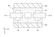
- FIG. 2 shows an example of the configuration of the frame 50 along line AA in FIG. 1 in a cross-sectional view parallel to the XZ plane.
- the frame 50 has a conductive main body 500 and slits 51 formed on both sides of the main body 500 in the width direction.
- the slits 51 hold the side edges of the reflective panel 10.
- the side edge of the reflective panel 10 is an edge along the Y direction in FIG.
- the main body 500 is formed with a cavity 52 that communicates with the slit 51, a groove 53 provided in the cavity 52, and a hollow 55 that does not communicate with the cavity 52 and the groove 53, but is not limited to this example.
- the groove 53 is provided at a position facing the slit 51 with the cavity 52 in between, and holds the side edge of the reflective panel 10 inserted through the slit 51. By providing the cavity 52 and the hollow 55 in the frame 50, the weight of the frame 50 can be reduced. By providing the groove 53 in the cavity 52, the reflective panel 10 can be held firmly.
- a non-conductive cover 501 made of resin or the like may be provided on the outer surface of the main body 500, but the cover 501 is not essential. When the cover 501 is provided, the cover 501 functions as a protection member that protects the frame 50.
- FIG. 3 shows a state in which the reflective panel 10 is inserted into the frame 50 in a cross-sectional view parallel to the XZ plane.
- the reflective panels 10-1 and 10-2 are inserted through the slits 51 (see FIG. 2) on both sides of the main body 500.
- the reflective panels 10-1 and 10-2 may or may not necessarily be inserted deep into the groove 53 of the cavity 52 (see FIG. 2) and abut against the main body 500.
- a portion of body 500 may be formed of a non-conductive material.
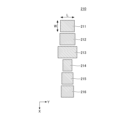
- FIG. 4 shows an example of the layer structure of the reflective panel 10.
- This layer structure is a layer structure in the thickness (Z) direction of the reflective panel 10.
- the reflective panel 10 includes a dielectric layer 14, a conductive layer 15 provided on one surface of the dielectric layer 14, a ground layer 13 provided on the opposite surface, and a first layer covering the conductive layer 15. It has an intermediate layer 16 and a second intermediate layer covering the ground layer 13.
- the first intermediate layer 16 is an adhesive film, and a first dielectric substrate 17 is bonded to the first intermediate layer 16 .
- the second intermediate layer 12 is an adhesive film, and the second dielectric substrate 11 is bonded to the second intermediate layer 12 .
- the dielectric layer 14 is an insulating polymer film made of polycarbonate, cycloolefin polymer (COP), polyethylene terephthalate (PET), fluororesin, etc., and has a thickness of about 0.3 mm to 1.0 mm.
- the dielectric layer 14 may be any material as long as it has a relative dielectric constant and a dielectric loss tangent suitable for realizing the target reflection characteristics.
- the conductive layer 15 forms the reflective surface of the reflective panel 10.
- the reflective surface formed by the conductive layer 15 may include a metasurface whose reflective properties are artificially controlled.
- the conductive layer 15 includes a conductive pattern 151 including a periodic pattern and an adhesive layer 152 that fixes the conductive pattern 151 to the dielectric layer 14 .
- the conductive pattern 151 is made of a good conductor such as Cu, Ni, or Ag, and has a thickness of about 10 ⁇ m to 50 ⁇ m.
- the adhesive layer 152 can support the conductive pattern 151 and fix it to the dielectric layer 14.
- thermoplastic resins such as vinyl acetate resin, acrylic resin, cellulose resin, and silicone resin may be used.
- the thickness of the adhesive layer 152 is approximately 5 ⁇ m to 50 ⁇ m.
- the first intermediate layer 16 covering the conductive layer 15 protects the surface of the conductive layer 15 and is used for bonding the first dielectric substrate 17.
- the first intermediate layer 16 desirably has durability and moisture resistance, and can be made of, for example, ethylene-vinyl acetate (EVA) copolymer or cycloolefin polymer (COP).
- EVA ethylene-vinyl acetate
- COP cycloolefin polymer
- the thickness of the first intermediate layer 16 is 10 ⁇ m to 400 ⁇ m.
- a first dielectric substrate 17 is bonded to the first intermediate layer 16 .
- the first dielectric substrate 17 is desirably made of a material with excellent impact resistance, durability, and transparency.
- the first dielectric substrate 17 polycarbonate, acrylic resin, PET, etc. can be used.
- the thickness of the first dielectric substrate 17 is, for example, 1.0 mm to 10.0 mm.
- the second intermediate layer 12 covering the ground layer 13 protects the surface of the ground layer 13 and is used for bonding the second dielectric substrate 11.
- the second intermediate layer 12 desirably has durability and moisture resistance, and can be made of, for example, EVA or COP.
- the thickness of the second intermediate layer 12 is 10 ⁇ m to 400 ⁇ m.
- a second dielectric substrate 11 is bonded to the second intermediate layer 12.
- the second dielectric substrate 11 is desirably made of a material with excellent impact resistance, durability, and transparency.
- the second dielectric substrate 11 polycarbonate, acrylic resin, PET, or the like can be used.
- the thickness of the second dielectric substrate 11 is, for example, 1.0 mm to 10.0 mm.
- the conductive layer 15 By covering the conductive layer 15 with the first intermediate layer 16 and bonding the first dielectric substrate 17, moisture and air are prevented from entering the surface of the conductive layer 15, and surface deterioration of the conductive pattern 151 is suppressed. be done.
- the ground layer 13 By covering the ground layer 13 with the second intermediate layer 12 and bonding the second dielectric substrate 11, moisture and air are prevented from entering the surface of the ground layer 13, and surface deterioration of the ground layer 13 is suppressed. be done. Thereby, the capacitance between the ground layer 13 and the conductive pattern 151 is maintained constant, and the designed magnitude of the phase delay can be maintained. That is, it is possible to maintain the reflection efficiency of radio waves in the designed direction.
- the reflection characteristics are evaluated by changing the area occupancy of the conductive pattern 151 of the reflective panel 10 having the layer structure shown in FIG. 4. It is predicted that the higher the area occupation rate of the conductive pattern 151, the better the reflection efficiency will be.
- the electromagnetic wave reflecting device 60 when used indoors or outdoors, such as on a road, in a park, in a factory, in a commercial facility, or in an office, it is desirable that the electromagnetic wave reflection device 60 has some degree of transparency in order to let in natural light and illumination light. Therefore, the goal is a design that can maintain a high reflection efficiency while maintaining a transmittance of 35% or more, more preferably 40%.
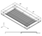
- FIG. 5 shows a model 21 of the conductive pattern 151 used for evaluating the reflective panel 10.
- the model 21 for evaluation includes a periodic array of unit cells (also called "supercells") 210.
- the unit cells 210 are arranged in 6 rows in the X direction and 36 rows in the Y direction, forming a metasurface that reflects electromagnetic waves at an angle different from the incident angle.
- FIG. 6 is a schematic diagram showing the configuration of the unit cell 210 of the model 21.
- Unit cell 210 is formed of six metal patches 211, 212, 213, 214, 215, and 216.
- the width (W) direction and length (L) of the metal patches 211-216 correspond to the width (X) direction and height (Y) direction of the reflective panel 10 in FIG. 1, respectively.
- the metal patches 211 to 216 have the same width W and different lengths L, but their central axes are aligned (the Y coordinate position of the central axes is constant).
- the pitch in the X direction is constant.
- the phase of reflection is controlled by the shape and size of the metal patches 211-216, and a reflected beam is formed in a desired direction by superimposing the reflected waves.
- the design is such that the peak of the reflected wave of the vertically incident electromagnetic wave (incident angle 0°) appears in the direction of 50° from the normal.
- the evaluation method was to use general-purpose three-dimensional electromagnetic field simulation software to inject a plane wave of 28.0 GHz at an incident angle of 0° using the conductive pattern 151 of the model 21 in FIG. Analyze the scattering cross section.
- the scattering cross section, or radar cross section (RCS) is used as an indicator of the ability to reflect incident electromagnetic waves.
- the power reflection efficiency of the metasurface is a value obtained by dividing the power reflection efficiency obtained from the gain value by the correction value.
- E MR be the reflected electric field on the lossless metasurface determined by the simulation model pattern in FIG. 5
- E PEC be the reflected electric field on the ideal conductive plate
- ⁇ is the angle of incidence on the metasurface
- ⁇ is the corresponding angle of reflection for regular reflection.
- FIG. 7 shows an analysis space 101 for electromagnetic wave simulation.
- the thickness direction of the layered structure in Fig. 4 is the Z direction
- the width direction of the metal patch of model 21 in Fig. 5 is the X direction
- the length direction is the Y direction
- the analysis space is (size in the X direction) x (size in the Y direction). size) x (size in Z direction).
- the size of the analysis space 101 when the frequency of the incident electromagnetic wave is 28.0 GHz is 83.9 mm x 192.6 mm x 3.7 mm.
- the boundary condition is a design in which electromagnetic wave absorbers 102 are arranged around the analysis space 101.
- FIG. 8A is a schematic diagram of the XY plane of the analysis space 101 surrounded by the electromagnetic wave absorber 102
- FIG. 8B is a schematic diagram of the XZ plane of the analysis space 101
- FIG. 8C is a schematic diagram of the YZ plane of the analysis space 101.
- the power reflection efficiency is calculated by changing the size and area occupation rate of the metal patch of the model 21 that constitutes the conductive pattern 151.
- a polycarbonate film with a thickness of 0.7 mm is used as the dielectric layer 14.
- a ground layer 13 made of an Ag-based multilayer film with a thickness of 0.36 mm is set on one side of the polycarbonate film, and a conductive layer 15 is set on the other side of the polycarbonate film.
- the conductive layer 15 has a conductive pattern 151 made of copper foil with a thickness of 0.03 mm on an adhesive layer 152 with a thickness of 0.01 mm.
- the shapes of the adhesive layer 152 and the conductive pattern 151, that is, the occupancy rates are the same.
- Both the intermediate layer 12 covering the ground layer 13 and the intermediate layer 16 covering the conductive layer 15 are made of EVA with a thickness of 400 ⁇ m.
- Polycarbonate sheets with a thickness of 2.0 mm are bonded to the intermediate layers 12 and 16 as dielectric substrates 11 and 17, respectively.
- the six metal patches 211-216 of the unit cell 210 of the conductive pattern 151 have a rectangular shape with a uniform width W of 0.7 mm, and lengths L of 2.8478 mm, 3.0043 mm, 3.7000 mm, and 1.0 mm, respectively. 7348mm, 2.5174mm, and 2.6925mm.
- the widthwise gap between the metal patches is uniformly 1.6283 mm.
- the area occupation rate of this conductive pattern 151 is 15.4%, and the transmittance of the entire layered structure shown in FIG. 4 is 55.5%.
- the gain value (peak value of the reflected waveform) at 50° in the RCS plot is 11.5900 dB.
- a power reflection efficiency of 70% or more can be obtained.
- the state of the reflective panel 10 having this layered structure after being left standing in an environment of 60° C. and 95% humidity for 500 hours is calculated.
- the gain value at 50° of the RCS plot is 11.1566 dB.
- Example 2 the layer structure is the same as in Example 1, but the dimensions and area occupation rate of the conductive pattern 151 are changed. That is, a ground layer 13 made of a 0.36 mm thick Ag film is set on one side of a 0.7 mm thick polycarbonate film as the dielectric layer 14, and a conductive layer 15 is set on the other side.
- the conductive layer 15 has a conductive pattern 151 made of copper foil with a thickness of 0.03 mm on an adhesive layer 152 with a thickness of 0.01 mm.
- the shapes of the adhesive layer 152 and the conductive pattern 151, that is, the occupancy rates are the same.
- Both the intermediate layer 12 covering the ground layer 13 and the intermediate layer 16 covering the conductive layer 15 are made of EVA with a thickness of 400 ⁇ m.
- Polycarbonate sheets with a thickness of 2.0 mm are bonded to the intermediate layers 12 and 16 as dielectric substrates 11 and 17, respectively.
- the six metal patches 211-216 of the unit cell 210 of the conductive pattern 151 have a rectangular shape with a uniform width W of 1.0 mm, and lengths L of 2.8091 mm, 2.9861 mm, 3.7461 mm, and 1.0 mm, respectively. 2505mm, 2.3214mm, and 2.5348mm.
- the widthwise gap between the metal patches is uniformly 1.3283 mm.
- the area occupation rate of this conductive pattern 151 is 20.9%, and the transmittance of the entire layer structure is 51.9%.
- Example 3 the layer structure is the same as in Examples 1 and 2, but the dimensions and area occupation rate of the conductive pattern 151 are changed. That is, a ground layer 13 made of a 0.36 mm thick Ag film is set on one side of a 0.7 mm thick polycarbonate film as the dielectric layer 14, and a conductive layer 15 is set on the other side.
- the conductive layer 15 has a conductive pattern 151 made of copper foil with a thickness of 0.03 mm on an adhesive layer 152 with a thickness of 0.01 mm.
- the shapes, ie, the occupancies, of the adhesive layer 152 and the conductive pattern 151 are the same.
- Both the intermediate layer 12 covering the ground layer 13 and the intermediate layer 16 covering the conductive layer 15 are made of EVA with a thickness of 400 ⁇ m.
- Polycarbonate sheets with a thickness of 2.0 mm are bonded to the intermediate layers 12 and 16 as dielectric substrates 11 and 17, respectively.
- the six metal patches 211-216 of the unit cell 210 of the conductive pattern 151 have a rectangular shape with a uniform width W of 1.5 mm, and lengths L of 2.6477 mm, 2.8607 mm, 4.0544 mm, and 1.5 mm, respectively. 2510mm, 2.1591mm, and 2.3923mm.
- the widthwise gap between the metal patches is uniformly 0.8283 mm.
- the area occupation rate of this conductive pattern 151 is 30.8%, and the transmittance of the entire layer structure is 46.0%.
- Example 4 the layer structure is the same as in Examples 1-3, but the dimensions and area occupation rate of the conductive pattern 151 are changed. That is, a ground layer 13 made of a 0.36 mm thick Ag film is set on one side of a 0.7 mm thick polycarbonate film as the dielectric layer 14, and a conductive layer 15 is set on the other side.
- the conductive layer 15 has a conductive pattern 151 made of copper foil with a thickness of 0.03 mm on an adhesive layer 152 with a thickness of 0.01 mm.
- the shapes, ie, the occupancies, of the adhesive layer 152 and the conductive pattern 151 are the same.
- Both the intermediate layer 12 covering the ground layer 13 and the intermediate layer 16 covering the conductive layer 15 are made of EVA with a thickness of 400 ⁇ m.
- Polycarbonate sheets with a thickness of 2.0 mm are bonded to the intermediate layers 12 and 16 as dielectric substrates 11 and 17, respectively.
- the six metal patches 211-216 of the unit cell 210 of the conductive pattern 151 have a rectangular shape with a uniform width W of 2.1 mm, and lengths L of 2.6000 mm, 2.8354 mm, 3.5531 mm, and 1.5 mm, respectively. 6459mm, 2.1321mm, and 2.3600mm.
- the widthwise gap between the metal patches is uniformly 0.2283 mm.
- the area occupation rate of this conductive pattern 151 is 42.4%, and the transmittance of the entire layered structure is 38.8%.
- Example 5 In Example 5, the same layer structure as in Example 1-4 and the same conductive pattern 151 as in Example 4 are used, but the thickness of the Cu conductive pattern 151 supported on the adhesive layer 152 with a thickness of 0.01 mm is , increase to 0.05mm.
- the intermediate layer 16 covering the adhesive layer 152 and the conductive pattern 151, and the intermediate layer 12 covering the Ag ground layer 13 are both made of EVA with a thickness of 400 ⁇ m.
- Polycarbonate sheets with a thickness of 2.0 mm are bonded to the intermediate layers 12 and 16 as dielectric substrates 11 and 17, respectively.
- the six metal patches 211 to 216 of the unit cell 210 of the conductive pattern 151 have a rectangular shape with a uniform width W of 2.1 mm, as in Example 4, and lengths L of 2.6000 mm, 2.8354 mm, and 2.8354 mm, respectively. 3.5531mm, 1.6459mm, 2.1321mm, 2.3600mm.
- the widthwise gap between the metal patches is uniformly 0.2283 mm.
- the area occupation rate of this conductive pattern 151 is 42.4%, and the transmittance of the entire layered structure is 38.8%.
- Example 5 by increasing the thickness of the conductive pattern to 0.05 mm while maintaining a sufficient area occupation rate of the conductive pattern 151, the power reflection efficiency was slightly improved compared to Example 4. Recognize.
- Example 6 the same layer structure as in Example 1-5 and the same conductive pattern 151 as in Example 4-5 are used, but the Cu conductive pattern 151 supported on an adhesive layer 152 with a thickness of 0.01 mm is used. Reduce the thickness to 0.01 mm.
- the intermediate layer 16 covering the adhesive layer 152 and the conductive pattern 151, and the intermediate layer 12 covering the Ag ground layer 13 are both made of EVA with a thickness of 400 ⁇ m. Polycarbonate sheets with a thickness of 2.0 mm are bonded to the intermediate layers 12 and 16 as dielectric substrates 11 and 17, respectively.
- the six metal patches 211-216 of the unit cell 210 of the conductive pattern 151 have a rectangular shape with a uniform width W of 2.1 mm and a length L of 2.6000 mm and 2.6000 mm, respectively, as in Example 4-5. 8354mm, 3.5531mm, 1.6459mm, 2.1321mm, 2.3600mm. The widthwise gap between the metal patches is uniformly 0.2283 mm.
- the area occupation rate of this conductive pattern 151 is 42.4%, and the transmittance of the entire layered structure is 38.8%.
- the gain value at 50° of the RCS plot is 11.1746 dB.
- Example 7 a conductive pattern 151 having the same layer structure as in Example 1-6 and the same shape as in Example 4-6 is used, but a conductive pattern of Cu supported on an adhesive layer 152 with a thickness of 0.01 mm is used.
- the thickness of the intermediate layer 151 is set to 0.03 mm, and the thickness of the intermediate layers 16 and 12, which respectively cover the conductive pattern 151 and the ground layer 13 above and below the dielectric layer 14, is reduced to 100 ⁇ m.
- the intermediate layer 16 that covers the adhesive layer 152 and the conductive pattern 151 and the intermediate layer 12 that covers the Ag ground layer 13 are both made of EVA with a thickness of 100 ⁇ m. and 17, a 2.0 mm thick polycarbonate sheet is adhered.
- the six metal patches 211-216 of the unit cell 210 of the conductive pattern 151 have a rectangular shape with a uniform width W of 2.1 mm and a length L of 2.6000 mm and 2.6000 mm, respectively, as in Example 4-6. 8354mm, 3.5531mm, 1.6459mm, 2.1321mm, 2.3600mm. The widthwise gap between the metal patches is uniformly 0.2283 mm.
- the area occupation rate of this conductive pattern 151 is 42.4%, and the transmittance of the entire layered structure is 38.8%.
- the gain value at 50° in the RCS plot is 11.4943 dB.
- Example 8 a conductive pattern 151 having the same layer structure as Example 1-7, the same thickness, and the same shape as Example 7, and intermediate layers 16 and 12 having the same thickness are used.
- the thickness of dielectric substrates 17 and 11 bonded to 12 is reduced to 1.0 mm.
- EVA with a thickness of 100 ⁇ m is used as the intermediate layer 16 that covers the adhesive layer 152 and the conductive pattern 151, and a polycarbonate sheet with a thickness of 1.0 mm is adhered to the intermediate layer 16.
- EVA with a thickness of 100 ⁇ m is used as the intermediate layer 12 covering the ground layer 13 of Ag, and a polycarbonate sheet with a thickness of 1.0 mm is adhered to the intermediate layer 12.
- the six metal patches 211-216 of the unit cell 210 of the conductive pattern 151 have a rectangular shape with a uniform width W of 2.1 mm and a length L of 2.6000 mm and 2.6000 mm, respectively, as in Example 4-7. 8354mm, 3.5531mm, 1.6459mm, 2.1321mm, 2.3600mm. The widthwise gap between the metal patches is uniformly 0.2283 mm.
- the area occupation rate of this conductive pattern 151 is 42.4%, and the transmittance of the entire layered structure is 38.8%.
- the gain value at 50° in the RCS plot is 11.4943 dB.
- Comparative Example 1 a conductive pattern 151 having the same layer structure and the same thickness as in Example 1-4 is used, but the dimensions and area occupation rate of the conductive pattern 151 are changed.
- EVA with a thickness of 400 ⁇ m is used as the intermediate layer 16 that covers the adhesive layer 152 with a thickness of 0.01 mm and the Cu conductive pattern 151 with a thickness of 0.03 mm, and a polycarbonate sheet with a thickness of 2.0 mm is adhered to the intermediate layer 16.
- EVA with a thickness of 400 ⁇ m is used as the intermediate layer 12 covering the ground layer 13 of Ag with a thickness of 0.36 mm, and a polycarbonate sheet with a thickness of 2.0 mm is adhered to the intermediate layer 12.
- the six metal patches 211 to 216 of the unit cell 210 of the conductive pattern 151 have a rectangular shape with a uniform width W of 0.4 mm, and lengths L of 2.9751 mm, 3.0739 mm, 3.7536 mm, and 2. .0344mm, 2.7300mm, and 2.8497mm.
- the widthwise gap between the metal patches is uniformly 1.9283 mm.
- the area occupation rate of this conductive pattern 151 is 9.3%, and the transmittance of the entire layered structure is 59.1%.
- Comparative Example 2 a conductive pattern 151 having the same layer structure and the same planar shape as Comparative Example 1 is used, but the thickness of the conductive pattern 151 is increased to 0.05 mm. Other conditions were the same as in Comparative Example 1.
- the six metal patches 211 to 216 of the unit cell 210 of the conductive pattern 151 have a rectangular shape with a uniform width W of 0.4 mm, and lengths L of 2.9751 mm, 3.0739 mm, 3.7536 mm, and 2. .0344mm, 2.7300mm, and 2.8497mm.
- the widthwise gap between the metal patches is uniformly 1.9283 mm.
- the area occupation rate of the conductive pattern 151 is 9.3%, the same as in Comparative Example 1, and the transmittance of the entire layer structure is 59.1%.
- Comparative Example 3 In Comparative Example 2, a conductive pattern 151 having the same layer structure and the same planar shape as Comparative Example 1-2 is used, but the thickness of the conductive pattern 151 is reduced to 0.001 mm. Other conditions were the same as in Comparative Example 1.
- the six metal patches 211 to 216 of the unit cell 210 of the conductive pattern 151 have a rectangular shape with a uniform width W of 0.4 mm, and lengths L of 2.9751 mm, 3.0739 mm, 3.7536 mm, and 2. .0344mm, 2.7300mm, and 2.8497mm.
- the widthwise gap between the metal patches is uniformly 1.9283 mm.
- the area occupation rate of the conductive pattern 151 is 9.3%, the same as in Comparative Example 1-2, and the transmittance of the entire layer structure is 59.1%.
- the area of the conductive pattern 151 is The occupancy rate is preferably 10% or more and 45% or less, more preferably 15% or more and 45% or less.
- the thickness of the conductive pattern 151 at this time is 0.01 or more and 0.05 mm or less. This is considered to be because when the area occupation rate of the conductive pattern 151 becomes less than 10%, the electric fields of the incident electromagnetic wave and the reflected wave concentrate on the surrounding dielectric material, and the reflection efficiency in the designed angle and direction decreases.
- the thickness of the intermediate layers 16 and 12 covering the conductive pattern 151 and the ground layer 13 may be such that it can ensure moisture resistance and protection for the conductor and can bond the dielectric substrates 17 and 11.
- An adhesive film with a thickness of 10 ⁇ m or more and 400 ⁇ m or less can be used.
- the outermost dielectric substrates 17 and 11 may be transparent to the frequency used, highly transparent to visible light, and have excellent durability.On the other hand, the thickness and weight of the reflective panel 10 are large. To avoid excessive thickness, the thickness is desirably 1.0 mm or more and 5.0 mm or less, more preferably 1.0 mm or more and 3.0 mm or less.
- FIG. 9A shows the radiation pattern and orthogonal coordinate plot of the layered reflective panel 10 of Example 1 in its initial state.
- FIG. 9B shows a radiation pattern and an orthogonal coordinate plot after the reflective panel 10 of Example 1 was left standing in an environment with a temperature of 60° C. and a humidity of 90% for 500 hours.
- a main peak is observed in the +50° direction with respect to normal incidence, and a side peak is observed in the ⁇ 50° direction.
- reflected radio waves cover a range of 30° to 80° in the positive and negative directions.
- the radiation pattern and peak size shown in FIG. 9A are maintained even after the reflective panel 10 is left in a harsh environment for 500 hours.
- the electromagnetic wave reflecting device and the electromagnetic wave reflecting fence using the reflective panel of the embodiment have an effect of improving the radio wave propagation environment and have excellent environmental resistance, and are excellent for application in harsh environments such as highways and construction site fences. .
- the electromagnetic wave reflecting device of the embodiment is not limited to the configuration example described above.
- the reflection angle with respect to normal incidence can be appropriately designed in the range of 35° or more and less than 90° by designing the size, shape, and pitch of the conductive pattern 151 and the dielectric constant of the dielectric layer 14.
- the in-plane size of the reflective panel 10 of the electromagnetic wave reflecting device can be appropriately selected from a range of 30 cm x 30 cm to 3 m x 3 m.
- the entire surface of the reflective panel 10 may be made into a metasurface, or a part may be made into a metasurface and the rest may be made into a specular reflective surface.
- the area occupation rate of the conductive pattern 151 forming the metasurface provided on part or all of the reflective surface may be set to 10% or more and 45% or less. In applications where high transmittance is not required, priority may be given to reflection efficiency by setting the area occupation rate of the conductive pattern 151 higher than 45%.
- Dielectric substrate Dielectric substrate (second dielectric substrate) 12 Middle layer (second middle layer) 13 Ground layer 14 Dielectric layer 15 Conductive layer 151 Conductive pattern 152 Adhesive layer 16 Intermediate layer (first intermediate layer) 17 Dielectric substrate (first dielectric substrate) 50 frame (side frame) 56 Legs 57 Top frame 58 Bottom frame 60, 60-1, 60-2, 60-3 Electromagnetic wave reflecting device 100 Electromagnetic wave reflecting fence 210 Unit cell
Landscapes
- Physics & Mathematics (AREA)
- Electromagnetism (AREA)
- Aerials With Secondary Devices (AREA)
Abstract
La présente invention supprime la réduction de l'efficacité de réflexion dans un dispositif de réflexion d'ondes électromagnétiques installé à l'intérieur ou à l'extérieur. Ledit dispositif de réflexion d'onde électromagnétique comprend : un panneau de réflexion qui réfléchit des ondes radio d'une bande souhaitée sélectionnée parmi des bandes de fréquence entre 1 GHz et 170 GHz inclus; et un cadre qui maintient le panneau de réflexion. Le panneau de réflexion comprend : une couche diélectrique; des motifs conducteurs périodiques disposés sur une surface de la couche diélectrique; une couche de masse disposée sur l'autre surface de la couche diélectrique; une première couche intermédiaire qui recouvre les motifs conducteurs; un premier substrat diélectrique relié aux motifs conducteurs par la première couche intermédiaire; une seconde couche intermédiaire qui recouvre la couche de masse; et un second substrat diélectrique relié à la couche de masse par la seconde couche intermédiaire.
Applications Claiming Priority (2)
| Application Number | Priority Date | Filing Date | Title |
|---|---|---|---|
| JP2022-089848 | 2022-06-01 | ||
| JP2022089848 | 2022-06-01 |
Publications (1)
| Publication Number | Publication Date |
|---|---|
| WO2023233928A1 true WO2023233928A1 (fr) | 2023-12-07 |
Family
ID=89026305
Family Applications (1)
| Application Number | Title | Priority Date | Filing Date |
|---|---|---|---|
| PCT/JP2023/017289 WO2023233928A1 (fr) | 2022-06-01 | 2023-05-08 | Dispositif de réflexion d'ondes électromagnétiques, barrière de réflexion d'ondes électromagnétiques et panneau de réflexion |
Country Status (1)
| Country | Link |
|---|---|
| WO (1) | WO2023233928A1 (fr) |
Citations (4)
| Publication number | Priority date | Publication date | Assignee | Title |
|---|---|---|---|---|
| JP2018110193A (ja) * | 2017-01-05 | 2018-07-12 | 住友電工プリントサーキット株式会社 | プリント配線用原板及びプリント配線板 |
| WO2021199504A1 (fr) * | 2020-03-31 | 2021-10-07 | Agc株式会社 | Système de transmission sans fil |
| WO2022070901A1 (fr) * | 2020-09-29 | 2022-04-07 | 日東電工株式会社 | Antenne à ondes millimétriques |
| JP2022072812A (ja) * | 2020-10-30 | 2022-05-17 | 電気興業株式会社 | 可変リフレクトアレーおよび可変リフレクトアレーの設計方法 |
-
2023
- 2023-05-08 WO PCT/JP2023/017289 patent/WO2023233928A1/fr unknown
Patent Citations (4)
| Publication number | Priority date | Publication date | Assignee | Title |
|---|---|---|---|---|
| JP2018110193A (ja) * | 2017-01-05 | 2018-07-12 | 住友電工プリントサーキット株式会社 | プリント配線用原板及びプリント配線板 |
| WO2021199504A1 (fr) * | 2020-03-31 | 2021-10-07 | Agc株式会社 | Système de transmission sans fil |
| WO2022070901A1 (fr) * | 2020-09-29 | 2022-04-07 | 日東電工株式会社 | Antenne à ondes millimétriques |
| JP2022072812A (ja) * | 2020-10-30 | 2022-05-17 | 電気興業株式会社 | 可変リフレクトアレーおよび可変リフレクトアレーの設計方法 |
Similar Documents
| Publication | Publication Date | Title |
|---|---|---|
| US8164506B2 (en) | Electromagnetic absorber using resistive material | |
| US20220200156A1 (en) | Antenna unit and window glass | |
| EP4287405A1 (fr) | Structure et matériau de construction | |
| US20100001918A1 (en) | Passive repeater antenna | |
| CN102723597B (zh) | 超材料天线罩及天线系统 | |
| WO2023233928A1 (fr) | Dispositif de réflexion d'ondes électromagnétiques, barrière de réflexion d'ondes électromagnétiques et panneau de réflexion | |
| US12057631B2 (en) | Antenna unit and window glass | |
| WO2023120471A1 (fr) | Condensateur d'ondes radio, vitre et système de communication par ondes radio | |
| WO2023233921A1 (fr) | Dispositif de réflexion d'ondes électromagnétiques, barrière de réflexion d'ondes électromagnétiques et panneau de réflexion | |
| WO2023233885A1 (fr) | Dispositif de réflexion d'ondes électromagnétiques, barrière de réflexion d'ondes électromagnétiques et panneau de réflexion | |
| WO2023233879A1 (fr) | Dispositif réfléchissant les ondes électromagnétiques, barrière réfléchissant les ondes électromagnétiques et panneau réfléchissant | |
| CN208460991U (zh) | 一种基于风车结构的平面反射阵列天线 | |
| WO2024029365A1 (fr) | Panneau réfléchissant, dispositif réfléchissant les ondes électromagnétiques l'utilisant, et barrière réfléchissant les ondes électromagnétiques | |
| CN114566811B (zh) | 一种模块化可拼接高环境适应性天线子阵 | |
| CN109980334A (zh) | 一种宽频带双极化天线 | |
| WO2024029325A1 (fr) | Panneau réfléchissant, dispositif réfléchissant les ondes électromagnétiques et clôture réfléchissant les ondes électromagnétiques | |
| CN206148623U (zh) | 宽频全向天线 | |
| WO2024135455A1 (fr) | Panneau réfléchissant et dispositif réfléchissant les ondes électromagnétiques | |
| CN209526201U (zh) | 宽频带双极化天线 | |
| WO2024135216A1 (fr) | Panneau de réflexion, dispositif de réflexion d'ondes électromagnétiques et barrière de réflexion d'ondes électromagnétiques | |
| CN112968296A (zh) | 一种应用于5g通信的透镜结构及5g基站 | |
| WO2023218887A1 (fr) | Dispositif de réflexion d'ondes électromagnétiques et barrière de réflexion d'ondes électromagnétiques | |
| EP4243199A1 (fr) | Ensemble d'antennes | |
| KR102492867B1 (ko) | 무전원 투명 안테나 | |
| WO2024106405A1 (fr) | Réflecteur d'ondes radio, procédé de production de réflecteur d'ondes radio, structure de réflexion d'ondes radio, système de réflexion d'ondes radio et dispositif de réflexion d'ondes radio |
Legal Events
| Date | Code | Title | Description |
|---|---|---|---|
| 121 | Ep: the epo has been informed by wipo that ep was designated in this application |
Ref document number: 23815689 Country of ref document: EP Kind code of ref document: A1 |