WO2023219052A1 - コンピュータ - Google Patents
コンピュータ Download PDFInfo
- Publication number
- WO2023219052A1 WO2023219052A1 PCT/JP2023/017244 JP2023017244W WO2023219052A1 WO 2023219052 A1 WO2023219052 A1 WO 2023219052A1 JP 2023017244 W JP2023017244 W JP 2023017244W WO 2023219052 A1 WO2023219052 A1 WO 2023219052A1
- Authority
- WO
- WIPO (PCT)
- Prior art keywords
- stroke image
- video signal
- pen
- computer
- temporary
- Prior art date
- Legal status (The legal status is an assumption and is not a legal conclusion. Google has not performed a legal analysis and makes no representation as to the accuracy of the status listed.)
- Ceased
Links
Images



Classifications
-
- G—PHYSICS
- G06—COMPUTING OR CALCULATING; COUNTING
- G06F—ELECTRIC DIGITAL DATA PROCESSING
- G06F3/00—Input arrangements for transferring data to be processed into a form capable of being handled by the computer; Output arrangements for transferring data from processing unit to output unit, e.g. interface arrangements
- G06F3/14—Digital output to display device ; Cooperation and interconnection of the display device with other functional units
-
- G—PHYSICS
- G06—COMPUTING OR CALCULATING; COUNTING
- G06F—ELECTRIC DIGITAL DATA PROCESSING
- G06F3/00—Input arrangements for transferring data to be processed into a form capable of being handled by the computer; Output arrangements for transferring data from processing unit to output unit, e.g. interface arrangements
- G06F3/01—Input arrangements or combined input and output arrangements for interaction between user and computer
- G06F3/03—Arrangements for converting the position or the displacement of a member into a coded form
- G06F3/033—Pointing devices displaced or positioned by the user, e.g. mice, trackballs, pens or joysticks; Accessories therefor
- G06F3/0354—Pointing devices displaced or positioned by the user, e.g. mice, trackballs, pens or joysticks; Accessories therefor with detection of two-dimensional [2D] relative movements between the device, or an operating part thereof, and a plane or surface, e.g. 2D mice, trackballs, pens or pucks
- G06F3/03545—Pens or stylus
-
- G—PHYSICS
- G06—COMPUTING OR CALCULATING; COUNTING
- G06F—ELECTRIC DIGITAL DATA PROCESSING
- G06F3/00—Input arrangements for transferring data to be processed into a form capable of being handled by the computer; Output arrangements for transferring data from processing unit to output unit, e.g. interface arrangements
- G06F3/01—Input arrangements or combined input and output arrangements for interaction between user and computer
- G06F3/03—Arrangements for converting the position or the displacement of a member into a coded form
- G06F3/041—Digitisers, e.g. for touch screens or touch pads, characterised by the transducing means
- G06F3/0416—Control or interface arrangements specially adapted for digitisers
- G06F3/04162—Control or interface arrangements specially adapted for digitisers for exchanging data with external devices, e.g. smart pens, via the digitiser sensing hardware
-
- G—PHYSICS
- G06—COMPUTING OR CALCULATING; COUNTING
- G06F—ELECTRIC DIGITAL DATA PROCESSING
- G06F3/00—Input arrangements for transferring data to be processed into a form capable of being handled by the computer; Output arrangements for transferring data from processing unit to output unit, e.g. interface arrangements
- G06F3/01—Input arrangements or combined input and output arrangements for interaction between user and computer
- G06F3/03—Arrangements for converting the position or the displacement of a member into a coded form
- G06F3/041—Digitisers, e.g. for touch screens or touch pads, characterised by the transducing means
- G06F3/044—Digitisers, e.g. for touch screens or touch pads, characterised by the transducing means by capacitive means
- G06F3/0441—Digitisers, e.g. for touch screens or touch pads, characterised by the transducing means by capacitive means using active external devices, e.g. active pens, for receiving changes in electrical potential transmitted by the digitiser, e.g. tablet driving signals
-
- G—PHYSICS
- G06—COMPUTING OR CALCULATING; COUNTING
- G06F—ELECTRIC DIGITAL DATA PROCESSING
- G06F3/00—Input arrangements for transferring data to be processed into a form capable of being handled by the computer; Output arrangements for transferring data from processing unit to output unit, e.g. interface arrangements
- G06F3/01—Input arrangements or combined input and output arrangements for interaction between user and computer
- G06F3/048—Interaction techniques based on graphical user interfaces [GUI]
- G06F3/0487—Interaction techniques based on graphical user interfaces [GUI] using specific features provided by the input device, e.g. functions controlled by the rotation of a mouse with dual sensing arrangements, or of the nature of the input device, e.g. tap gestures based on pressure sensed by a digitiser
- G06F3/0488—Interaction techniques based on graphical user interfaces [GUI] using specific features provided by the input device, e.g. functions controlled by the rotation of a mouse with dual sensing arrangements, or of the nature of the input device, e.g. tap gestures based on pressure sensed by a digitiser using a touch-screen or digitiser, e.g. input of commands through traced gestures
- G06F3/04883—Interaction techniques based on graphical user interfaces [GUI] using specific features provided by the input device, e.g. functions controlled by the rotation of a mouse with dual sensing arrangements, or of the nature of the input device, e.g. tap gestures based on pressure sensed by a digitiser using a touch-screen or digitiser, e.g. input of commands through traced gestures for inputting data by handwriting, e.g. gesture or text
-
- G—PHYSICS
- G06—COMPUTING OR CALCULATING; COUNTING
- G06T—IMAGE DATA PROCESSING OR GENERATION, IN GENERAL
- G06T11/00—Two-dimensional [2D] image generation
- G06T11/20—Drawing from basic elements
- G06T11/23—Drawing from basic elements using straight lines or curves
-
- G—PHYSICS
- G09—EDUCATION; CRYPTOGRAPHY; DISPLAY; ADVERTISING; SEALS
- G09G—ARRANGEMENTS OR CIRCUITS FOR CONTROL OF INDICATING DEVICES USING STATIC MEANS TO PRESENT VARIABLE INFORMATION
- G09G3/00—Control arrangements or circuits, of interest only in connection with visual indicators other than cathode-ray tubes
- G09G3/20—Control arrangements or circuits, of interest only in connection with visual indicators other than cathode-ray tubes for presentation of an assembly of a number of characters, e.g. a page, by composing the assembly by combination of individual elements arranged in a matrix no fixed position being assigned to or needed to be assigned to the individual characters or partial characters
- G09G3/2092—Details of a display terminals using a flat panel, the details relating to the control arrangement of the display terminal and to the interfaces thereto
- G09G3/2096—Details of the interface to the display terminal specific for a flat panel
-
- H—ELECTRICITY
- H04—ELECTRIC COMMUNICATION TECHNIQUE
- H04N—PICTORIAL COMMUNICATION, e.g. TELEVISION
- H04N5/00—Details of television systems
- H04N5/222—Studio circuitry; Studio devices; Studio equipment
- H04N5/262—Studio circuits, e.g. for mixing, switching-over, change of character of image, other special effects ; Cameras specially adapted for the electronic generation of special effects
- H04N5/265—Mixing
-
- G—PHYSICS
- G09—EDUCATION; CRYPTOGRAPHY; DISPLAY; ADVERTISING; SEALS
- G09G—ARRANGEMENTS OR CIRCUITS FOR CONTROL OF INDICATING DEVICES USING STATIC MEANS TO PRESENT VARIABLE INFORMATION
- G09G2320/00—Control of display operating conditions
- G09G2320/06—Adjustment of display parameters
- G09G2320/0666—Adjustment of display parameters for control of colour parameters, e.g. colour temperature
-
- G—PHYSICS
- G09—EDUCATION; CRYPTOGRAPHY; DISPLAY; ADVERTISING; SEALS
- G09G—ARRANGEMENTS OR CIRCUITS FOR CONTROL OF INDICATING DEVICES USING STATIC MEANS TO PRESENT VARIABLE INFORMATION
- G09G2340/00—Aspects of display data processing
- G09G2340/04—Changes in size, position or resolution of an image
- G09G2340/0407—Resolution change, inclusive of the use of different resolutions for different screen areas
- G09G2340/0435—Change or adaptation of the frame rate of the video stream
-
- G—PHYSICS
- G09—EDUCATION; CRYPTOGRAPHY; DISPLAY; ADVERTISING; SEALS
- G09G—ARRANGEMENTS OR CIRCUITS FOR CONTROL OF INDICATING DEVICES USING STATIC MEANS TO PRESENT VARIABLE INFORMATION
- G09G2340/00—Aspects of display data processing
- G09G2340/10—Mixing of images, i.e. displayed pixel being the result of an operation, e.g. adding, on the corresponding input pixels
-
- G—PHYSICS
- G09—EDUCATION; CRYPTOGRAPHY; DISPLAY; ADVERTISING; SEALS
- G09G—ARRANGEMENTS OR CIRCUITS FOR CONTROL OF INDICATING DEVICES USING STATIC MEANS TO PRESENT VARIABLE INFORMATION
- G09G2340/00—Aspects of display data processing
- G09G2340/12—Overlay of images, i.e. displayed pixel being the result of switching between the corresponding input pixels
- G09G2340/125—Overlay of images, i.e. displayed pixel being the result of switching between the corresponding input pixels wherein one of the images is motion video
-
- G—PHYSICS
- G09—EDUCATION; CRYPTOGRAPHY; DISPLAY; ADVERTISING; SEALS
- G09G—ARRANGEMENTS OR CIRCUITS FOR CONTROL OF INDICATING DEVICES USING STATIC MEANS TO PRESENT VARIABLE INFORMATION
- G09G2354/00—Aspects of interface with display user
Definitions
- the present invention relates to a computer, and particularly to a computer that can prevent display delays of stroke images.
- pen data data such as coordinate data indicating the pen position and pen pressure values sent by the pen (hereinafter referred to as "pen data”) is sent from the sensor controller connected to the touch sensor to the host processor. ) will be supplied.
- the host processor generates a stroke image representing a stroke based on the supplied pen data, and displays the generated stroke image on a display.
- Patent Document 1 discloses an example of a computer that supports pen input.
- an overlay engine is provided in the timing controller, which is a component of the display, in order to avoid delays in displaying stroke images due to processing delays within the computer.
- Coordinate data is sent directly to the engine.
- the overlay engine generates a temporary stroke image based on the coordinate data received from the sensor controller, and performs a process of updating a display frame received from the host processor using the generated temporary stroke image.
- Patent Document 2 discloses an example of a liquid crystal display device having a graphic processing circuit including a scaler upstream of a timing controller.
- Patent Document 1 Although the technique described in Patent Document 1 can prevent the display of stroke images from being delayed, there is a problem in that an overlay engine must be provided in the timing controller, which is a component of the display. Therefore, there is a need for a technique that can prevent the display delay of stroke images without providing an overlay engine in the timing controller.
- one of the objects of the present invention is to provide a computer that can prevent display delays of stroke images without providing an overlay engine in the timing controller.
- a computer includes a host processor that generates a stroke image representing a stroke represented by a series of coordinate data each representing the position of a pen within a touch surface, and a host processor that generates a video signal representing the generated stroke image; a timing controller that controls the potential of each of the plurality of gate lines provided based on the video signal; and a temporary stroke image generation processor that generates a temporary stroke image showing the same stroke as the stroke image in parallel with the host processor. , wherein the temporary stroke image is superimposed on the video signal before being supplied to the timing controller.
- a temporary stroke image showing the same stroke as the stroke image generated by the host processor is generated in parallel with the host processor and superimposed on the video signal before being supplied to the timing controller. It becomes possible to prevent display delays of stroke images without providing an overlay engine in the controller.
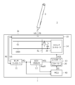
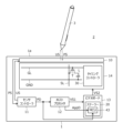
- FIG. 1 is a diagram showing the configuration of a position detection system 2 including a computer 1 according to a first embodiment of the present invention.
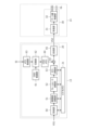
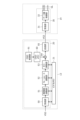
- 1 is a diagram showing the internal configuration of a video board 13 and a display panel 14 according to a first embodiment of the present invention.
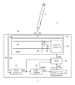
- FIG. FIG. 2 is a diagram showing the configuration of a position detection system 2 including a computer 1 according to a second embodiment of the present invention.
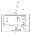
- FIG. 3 is a diagram showing the configuration of a position detection system 2 including a computer 1 according to a third embodiment of the present invention.
- FIG. 7 is a diagram showing the internal configuration of a video board 13 and a display panel 14 according to a third embodiment of the present invention.
- FIG. 3 is a diagram showing the configuration of a position detection system 2 including a computer 1 according to a fourth embodiment of the present invention.
- FIG. 7 is a diagram showing the internal configuration of a video board 13 and a display panel 14 according to a fourth embodiment of the present invention. It is a diagram showing the configuration of a position detection system 2 including a computer 1 according to a fifth embodiment of the present invention.
- FIG. 7 is a diagram showing the internal configuration of a video board 13 and a display panel 14 according to a fifth embodiment of the present invention.
- FIG. 1 is a diagram showing the configuration of a position detection system 2 including a computer 1 according to a first embodiment of the present invention. As shown in the figure, the position detection system 2 includes an electronic pen 3 in addition to the computer 1.
- the computer 1 is a computer, such as a tablet terminal or a smartphone, that has a panel surface 1a that serves as a touch surface and a display surface.
- the computer 1 may be a computer in which a touch panel or digitizer that supports pen input and a display for display are separately provided.
- the computer 1 and the electronic pen 3 are configured to be able to communicate bidirectionally using an electromagnetic induction method (EMR method).
- EMR method electromagnetic induction method
- the signal transmitted from the computer 1 to the electronic pen 3 through this communication will be referred to as an "uplink signal US”
- pen signal PS the signal transmitted from the electronic pen 3 to the computer 1
- the computer 1 and the electronic pen 3 may communicate using other methods such as an active electrostatic method.
- the computer 1 includes a sensor 10, a sensor controller 11, a host processor 12, a video board 13, a display panel 14, and an MCU (Micro Controller Unit) 40.
- the sensor 10 includes a plurality of loop coils arranged inside the panel surface 1a. One end of each loop coil is connected to the sensor controller 11, and the other end is grounded. Each loop coil supplies operating power and commands to the electronic pen 3 by coupling with a coil in the LC resonance circuit provided inside the electronic pen 3 by electromagnetic induction, and also supplies the pen signal PS transmitted by the electronic pen 3. plays the role of receiving.
- the sensor controller 11 is an integrated circuit that transmits an uplink signal US to the electronic pen 3 via the sensor 10 and receives a pen signal PS transmitted by the electronic pen 3 as a reflected signal in response to the uplink signal US.
- the uplink signal US is a signal for supplying operating power and commands to the electronic pen 3, and is periodically transmitted from the sensor controller 11.
- the electronic pen 3 stores power in a capacitor in the LC resonant circuit while receiving the uplink signal US, and transmits the pen signal PS using the stored power when the reception of the uplink signal US ends. It is configured like this.
- the sensor controller 11 performs a process of deriving coordinate data indicating the position of the electronic pen 3 within the panel surface 1a based on the received pen signal PS. Specifically, the distribution of the reception strength of the pen signal PS within the panel surface 1a is derived based on the reception strength of the pen signal PS in each loop coil, and the coordinate data of the position corresponding to the peak of the distribution is derived. Accordingly, coordinate data indicating the position of the electronic pen 3 is derived.
- the sensor controller 11 also performs processing to obtain a value indicating the pressure applied to the pen tip of the electronic pen 3 (hereinafter referred to as "pen pressure value") by detecting a phase change of the received pen signal PS.
- the capacitor constituting the LC resonance circuit of the electronic pen 3 includes a variable capacitor whose capacitance changes depending on the pressure applied to the nib of the electronic pen 3.
- the resonance frequency of the LC resonance circuit changes, and therefore the frequency of the pen signal PS also changes.
- the sensor controller 11 detects this change in frequency by detecting a phase change in the pen signal PS, and obtains a pen pressure value based on the result.
- the sensor controller 11 is configured to sequentially supply the derived coordinate data and the acquired writing pressure value to the host processor 12 and the MCU 40.
- these data supplied from the sensor controller 11 to the host processor 12 and MCU 40 may be collectively referred to as "pen data PD.”
- the host processor 12 is the central processing unit of the computer 1, and by reading programs from a storage device (not shown) and executing them, the host processor 12 executes the operating system of the computer 1 and various applications including a drawing application that supports pen input. configured.
- the processing performed by the host processor 12 includes processing to generate a video signal VS1 representing the desktop image of the computer 1 and supply it to the video board 13.
- the drawing application is an application that has a function of generating a stroke image indicating a stroke indicated by the pen data PD supplied from the sensor controller 11 and arranging the generated stroke image in a desktop image.
- the stroke is indicated by a series of coordinate data acquired while the pen pressure value is greater than 0 (that is, a value indicating that the pen tip of the electronic pen 3 is in contact with the panel surface 1a). This is the trajectory of the pen tip.
- a stroke image is a curve image obtained by giving a line width corresponding to a writing pressure value to an approximate curve formed by smoothly connecting a series of coordinate data forming a stroke. Examples of approximate curves include Bezier curves and Catmallom curves.
- the video board 13 is a device that converts the video signal VS1 supplied from the host processor 12 into a video signal VS2 that is a signal corresponding to the display panel 14. Specifically, it has a scaler 20, which is an integrated circuit, for adjusting the resolution, frame rate, and color of the video signal VS1 to values that can be supplied to the display panel 14, and the video signal after adjustment by the scaler 20.
- the display panel 14 is configured to supply a video signal VS2, which is the signal VS1.
- the display panel 14 is a device that displays an image according to the video signal VS2 on the panel surface 1a.
- the specific type of display panel 14 is not particularly limited, but may be, for example, a liquid crystal display or an organic EL display.
- the display panel 14 is a TFT (Thin Film Transistor) type liquid crystal display
- the display panel 14 includes a plurality of pixels each including a thin film transistor T and a liquid crystal element L, and a plurality of gates, as shown in FIG. It is configured to include a line GL, a plurality of signal lines SL, and a common ground wiring GND.
- FIG. 1 shows only one pixel, one gate line GL, one signal line SL, and the common ground wiring GND.
- the plurality of pixels are arranged in a matrix.
- Each gate line GL is commonly connected to each gate of a plurality of thin film transistors T arranged in a row direction
- each signal line SL is commonly connected to each source of a plurality of thin film transistors T arranged in a column direction.
- the display panel 14 performs the process of driving each pixel in units of rows. Specifically, the display panel 14 determines the potential to be applied to the liquid crystal element L of each pixel in the row of interest based on the video signal VS2, and applies the determined potential to each signal line SL. Then, the potential of the gate line GL of the row of interest is set to high. Then, a potential corresponding to the video signal VS2 is applied to each liquid crystal element L in the row of interest, so that an image corresponding to the video signal VS2 is displayed for the row of interest.
- the display panel 14 is configured with a timing controller 30.
- the timing controller 30 is a circuit that controls the potential of each of the plurality of gate lines GL based on the video signal VS2, and plays a role of controlling the timing of supplying the potential.
- the MCU 40 is a processing circuit that generates a temporary stroke image SI showing the same stroke as the stroke image generated by the host processor 12 in parallel with the host processor 12, and superimposes it on the video signal VS2 before being supplied to the timing controller 30. (temporary stroke image generation processor).
- the MCU 40 is configured to generate a temporary stroke image SI based on a series of pen data PD supplied from the sensor controller 11.
- the temporary stroke image SI may or may not have the exact same appearance as the stroke image generated by the host processor 12.
- the MCU 40 receives the above-described drawing data AppD from the host processor 12, and generates a temporary stroke image SI based on the received drawing data AppD.
- the MCU 40 may or may not receive all or part of the drawing data AppD set in the drawing application from the host processor 12.
- the MCU 40 When all or part of the drawing data AppD is received from the host processor 12, the MCU 40 generates a temporary stroke image SI based on the received drawing data AppD. If the drawing data AppD is not received from the host processor 12, the MCU 40 generates a temporary stroke image SI based on predetermined settings.
- the scaler 20 in this embodiment plays the role of actually superimposing the temporary stroke image SI supplied from the MCU 40 on the video signal VS2. This point will be explained in detail below with reference to FIG. 2.
- FIG. 2 is a diagram showing the internal configuration of the video board 13 and display panel 14 according to this embodiment.
- the video board 13 is configured to include a video memory 21 in addition to a scaler 20.
- the scaler 20 includes a reception section 50, a resolution adjustment section 51, a frame rate adjustment section 52, a color adjustment section 53, a mixer 54, a transmission section 55, an OSD (On-Screen Display) memory 60, an OSD control section 61, a switching section 62, It is configured to include a memory control section 63.
- the timing controller 30 includes a receiving section 31 and a gate line control section 32.
- the receiving unit 50 is a circuit that receives the video signal VS1 output by the host processor 12.
- the receiving unit 50 writes the received video signal VS1 into the video memory 21.
- the video memory 21 is a storage section configured to be able to store at least one screen worth of video signal VS1.
- the resolution adjustment unit 51 is a circuit that adjusts the resolution of the video signal VS1 received by the reception unit 50 to match the resolution of the display panel 14. For example, if the resolution of the video signal VS1 is FHD (1920 x 1080) and the resolution of the display panel 14 is 4K (3840 x 2160), the resolution adjustment unit 51 increases the resolution of the video signal VS1 by 4 times. Perform the processing to make it.
- the resolution adjustment unit 51 is configured to read the video signal VS1 to be adjusted from the video memory 21 and overwrite the video memory 21 with the adjusted video signal VS1.
- the frame rate adjustment unit 52 is a circuit that adjusts the frame rate of the video signal VS1 after adjustment by the resolution adjustment unit 51 to match the frame rate of the display panel 14. For example, if the frame rate of the video signal VS1 is 60 FPS and the frame rate of the display panel 14 is 30 FPS, the frame rate adjustment unit 52 performs processing to reduce the frame rate of the video signal VS1 to 1/2. .
- the frame rate adjustment unit 52 is configured to read the video signal VS1 to be adjusted from the video memory 21 and overwrite the video memory 21 with the adjusted video signal VS1.
- the color adjustment unit 53 is a circuit that adjusts the color of the video signal VS1 after adjustment by the frame rate adjustment unit 52 to match the color gamut of the display panel 14. For example, when the color gamut of the video signal VS1 is sRGB and the color gamut of the display panel 14 is NTSC, the color adjustment unit 53 performs processing to reconstruct the colors of the video signal VS1 using NTSC.
- the color adjustment unit 53 also has a function of detecting the type of video (natural image, baseball, animation, etc.) and performing color correction according to the detected type.
- the color adjustment unit 53 is configured to read the video signal VS1 to be adjusted from the video memory 21 and supply the adjusted video signal VS1 to the mixer 54.
- the OSD memory 60 is a storage unit that stores an image (hereinafter referred to as an "OSD image") to be superimposed on the video represented by the video signal VS1. Further, the OSD control unit 61 is a circuit that generates an OSD image according to a user operation and writes it into the OSD memory 60. Typically, the OSD image is a screen for adjusting the color and position of the screen that is displayed when the user presses a button provided on the edge of the display panel 14.
- the OSD memory 60 is configured to be able to store at least one screen worth of images.
- the mixer 54 is a circuit that superimposes the OSD image stored in the OSD memory 60 onto the video signal VS1 supplied from the color adjustment section 53. After processing by the mixer 54, the OSD image will be displayed on top of the video represented by the video signal VS1 (in the foreground).
- the transmitter 55 is a circuit that supplies the video signal VS2, which is the video signal VS1 processed by the mixer 54, to the display panel 14. Specifically, the video signal VS2 is input to the line buffer line by line, and the pixels stored in the line buffer are sequentially transmitted to the display panel 14. Further, the transmitter 55 is configured to transmit a horizontal synchronization signal (HSYNC) at a line break and a vertical synchronization signal (VSYNC) at a screen break. These horizontal synchronization signal (HSYNC) and vertical synchronization signal (VSYNC) also constitute a part of the video signal VS2.
- the receiving section 31 in the timing controller 30 is a circuit that receives the thus supplied video signal VS2 and supplies it to the gate line control section 32.
- the gate line control section 32 is a circuit that controls the potential of each of the plurality of gate lines GL based on the video signal VS2 supplied from the reception section 31.
- the memory control unit 63 is a circuit that writes the temporary stroke image SI generated by the MCU 40 into the OSD memory 60.
- a switching unit 62 is provided between the memory control unit 63 and the OSD control unit 61 and the OSD memory 60.
- the switching unit 62 connects the memory control unit 63 to the OSD memory 60 when the memory control unit 63 writes the temporary stroke image SI to the OSD memory 60, and connects the memory control unit 63 to the OSD memory 60 when the memory control unit 63 writes the temporary stroke image SI to the OSD memory 60. If not, it serves to connect the OSD control unit 61 to the OSD memory 60.
- the temporary stroke image SI is displayed on the image represented by the video signal VS1, giving priority to the OSD image.
- the temporary stroke image SI showing the same stroke as the stroke image generated by the host processor 12 is generated in parallel with the host processor 12, and the temporary stroke image SI is sent to the timing controller 30. Since it is superimposed on the video signal before being supplied, it is possible to display stroke images caused by processing delays within the computer 1 (such as waiting for processing in the host processor 12) without providing an overlay engine within the timing controller 30. This makes it possible to prevent delays.
- the temporary stroke image SI can be superimposed on the video signal VS2 using the existing mixer 54 and OSD memory 60, so that a dedicated overlay can be used as in Patent Document 1. Compared to the case where an engine and a buffer are provided, it is possible to reduce the circuit scale.
- FIG. 3 is a diagram showing the configuration of a position detection system 2 including a computer 1 according to a second embodiment of the present invention.
- the computer 1 according to the present embodiment differs from the computer 1 according to the first embodiment in that it has an MCU 41 instead of the MCU 40, and in other respects. , is similar to the computer 1 according to the first embodiment. Therefore, below, the explanation will be continued focusing on the differences from the computer 1 according to the first embodiment.
- the MCU 41 is the same as the MCU 40 according to the first embodiment in terms of the processing for generating the temporary stroke image SI, but supplies the generated temporary stroke image SI to the scaler 20, and causes the scaler 20 to superimpose it on the video signal VS2.
- the MCU 40 is different from the MCU 40 according to the first embodiment in that it superimposes itself on the video signal VS2 output from the video board 13 instead of processing it.
- the MCU 41 outputs each pixel of the temporary stroke image SI by referring to the vertical synchronization signal (VSYNC) and horizontal synchronization signal (HSYNC) described above.
- a video signal VS3 which is the superimposed video signal VS2, is directly supplied to the display panel 14 from the MCU 41.
- the display panel 14 that has received this supply executes processing for displaying an image on the panel surface 1a based on the video signal VS3 instead of the video signal VS2.
- the computer 1 also generates a temporary stroke image SI showing the same stroke as the stroke image generated by the host processor 12 in parallel with the host processor 12 and supplies it to the timing controller 30. Since the stroke image is superimposed on the video signal before being displayed, it is possible to prevent a display delay of the stroke image due to a processing delay in the computer 1 without providing an overlay engine in the timing controller 30.
- the generation and superimposition of the temporary stroke image SI can be executed without modifying the existing video board 13 and display panel 14, so that the timing can be improved as in Patent Document 1. This makes implementation easier than modifying the controller.
- FIG. 4 is a diagram showing the configuration of a position detection system 2 including a computer 1 according to a third embodiment of the present invention.
- the computer 1 according to the second embodiment differs from the computer 1 in that the information is supplied to the MCU 41 instead of the computer 13, and is otherwise similar to the computer 1 according to the second embodiment. Therefore, below, the explanation will be continued focusing on the differences from the computer 1 according to the second embodiment.
- the MCU 41 superimposes the temporary stroke image SI generated based on the series of pen data PD supplied from the sensor controller 11 on the video signal VS1 supplied from the host processor 12, thereby generating the video signal VS2. Perform generation.
- the video board 13 converts the video signal VS2 generated by the MCU 41 into a video signal VS3 that is a signal corresponding to the display panel 14, and supplies the video signal VS3 obtained by this conversion to the display panel 14.
- FIG. 5 is a diagram showing the internal configuration of the video board 13 and display panel 14 according to this embodiment.
- the input signal of the video board 13 according to this embodiment is the video signal VS2, and the output signal is the video signal VS3.
- the scaler 20 according to this embodiment does not include the switching section 62 and the memory control section 63. This is because in the present embodiment, the video signal VS2 on which the temporary stroke image SI has been superimposed is input to the video board 13, so there is no need for the scaler 20 to perform the process of superimposing the temporary stroke image SI on the video signal. This is due to a number of things.
- the computer 1 also generates a temporary stroke image SI showing the same stroke as the stroke image generated by the host processor 12 in parallel with the host processor 12 and supplies it to the timing controller 30. Since the stroke image is superimposed on the video signal before being displayed, it is possible to prevent a display delay of the stroke image due to a processing delay in the computer 1 without providing an overlay engine in the timing controller 30.
- the computer 1 since the computer 1 according to the present embodiment can also generate and superimpose the temporary stroke image SI without modifying the existing video board 13 and display panel 14, the timing controller This makes it easier to implement compared to modifying the .
- FIG. 6 is a diagram showing the configuration of a position detection system 2 including a computer 1 according to a fourth embodiment of the present invention.
- the computer 1 is different from the computer 1, but is otherwise similar to the computer 1 according to the first embodiment. Therefore, below, the explanation will be continued focusing on the differences from the computer 1 according to the first embodiment.
- the MCU 42 is provided inside the scaler 20, plays the role of the sensor controller 11 in the first embodiment, and, like the MCU 40 in the first embodiment, can generate the same stroke image as the stroke image generated by the host processor 12. It also plays the role of generating a temporary stroke image SI indicating , in parallel with the host processor 12, and superimposing it on the video signal VS2 before being supplied to the timing controller 30.
- the MCU 42 transmits an uplink signal US to the electronic pen 3 via the sensor 10, and receives a pen signal PS transmitted by the electronic pen 3 as a reflection signal in response to the uplink signal US. I do. It also performs a process of deriving or acquiring pen data PD based on the received pen signal PS and supplying it to the host processor 12. The host processor 12 generates a stroke image based on the pen data PD thus supplied.
- FIG. 7 is a diagram showing the internal configuration of the video board 13 and display panel 14 according to this embodiment. As can be understood from a comparison between the same figure and FIG. This differs from the video board 13 according to the first embodiment in this respect, and is the same as the video board 13 according to the first embodiment in other respects.
- the configuration of the display panel 14 is the same as that of the display panel 14 according to the first embodiment.
- the MCU 42 includes a pen signal processing section 71, a renderer 72, and an image memory 73.
- the AD conversion unit 70 is located before the pen signal processing unit 71 and plays the role of converting the pen signal PS received by each loop coil in the sensor 10 into a digital signal and supplying the digital signal to the pen signal processing unit 71. .
- the pen signal processing unit 71 transmits an uplink signal US to the electronic pen 3 via the sensor 10, and also generates an electronic signal as a reflected signal in response to the uplink signal US.
- a process of receiving the pen signal PS transmitted by the pen 3 is performed. It also performs a process of deriving or acquiring pen data PD based on the received pen signal PS and supplying it to the host processor 12.
- the host processor 12 generates a stroke image based on the pen data PD thus supplied.
- the pen signal processing unit 71 also supplies the derived or acquired pen data PD to the renderer 72.
- the renderer 72 is also supplied with drawing data AppD from the host processor 12 in addition to the pen data PD.
- the renderer 72 generates a temporary stroke image SI based on the pen data PD and drawing data AppD thus supplied, and writes the generated temporary stroke image SI into the image memory 73.
- the image memory 73 like the OSD memory 60, is a storage unit configured to be able to store at least one screen worth of images.
- the mixer 74 is a circuit that superimposes the temporary stroke image SI stored in the image memory 73 on the video signal VS1 output from the color adjustment section 53. After the processing by the mixer 74, the temporary stroke image SI will be displayed on top of the image represented by the video signal VS1 (in the foreground).
- the mixer 54 is provided after the mixer 74, and therefore, if there is an OSD image to be displayed, that OSD image will be displayed in front of the temporary stroke image SI.
- the computer 1 also generates a temporary stroke image SI showing the same stroke as the stroke image generated by the host processor 12 in parallel with the host processor 12 and supplies it to the timing controller 30. Since the stroke image is superimposed on the video signal before being displayed, it is possible to prevent a display delay of the stroke image due to a processing delay in the computer 1 without providing an overlay engine in the timing controller 30.
- the computer 1 it is possible to display the OSD image even when displaying the temporary stroke image SI, and moreover, it is possible to display the OSD image in front of the temporary stroke image SI. become.
- the temporary stroke image SI since the temporary stroke image SI is superimposed on the video signal VS1 at the subsequent stage of the color adjustment section 53, the temporary stroke image SI, which is a type of CG, can be used in the same way as an OSD image. , it becomes possible to display without being affected by color correction by the color adjustment section 53.
- FIG. 8 is a diagram showing the configuration of a position detection system 2 including a computer 1 according to a fifth embodiment of the present invention.
- the computer 1 according to the present embodiment is different from the computer 1 according to the first embodiment in that it has an MCU 43 instead of the MCU 40, and in other respects. , is similar to the computer 1 according to the first embodiment. Therefore, below, the explanation will be continued focusing on the differences from the computer 1 according to the first embodiment.
- the MCU 43 is provided inside the scaler 20 and generates a temporary stroke image SI indicating the same stroke as the stroke image generated by the host processor 12 in parallel with the host processor 12. It has the role of superimposing the video signal VS2 on the video signal VS2 before being supplied to the timing controller 30.
- the MCU 43 does not have a role as the sensor controller 11.
- FIG. 9 is a diagram showing the internal configuration of the video board 13 and display panel 14 according to this embodiment. As can be understood from a comparison between the same figure and FIG. This embodiment is different from the video board 13 according to the embodiment, and is otherwise similar to the video board 13 according to the first embodiment. The configuration of the display panel 14 is the same as that of the display panel 14 according to the first embodiment.
- the MCU 43 includes a matching processing section 80, a renderer 81, and an image memory 82.
- the matching processing section 80 is sequentially supplied with pen data PD from the sensor controller 11 .
- the matching processing unit 80 is configured to convert the coordinate data included in the supplied pen data PD into coordinate data according to the coordinate system of the display panel 14, and supply the pen data PD including the converted coordinate data to the renderer 81. Ru.
- the functions and operations of the renderer 81, image memory 82, and mixer 83 are similar to those of the renderer 72, image memory 73, and mixer 74 described in the fourth embodiment. Therefore, also in this embodiment, the temporary stroke image SI is displayed in front of the image represented by the video signal VS1 and behind the OSD image.
- the computer 1 also generates a temporary stroke image SI showing the same stroke as the stroke image generated by the host processor 12 in parallel with the host processor 12 and supplies it to the timing controller 30. Since the stroke image is superimposed on the video signal before being displayed, it is possible to prevent a display delay of the stroke image due to a processing delay in the computer 1 without providing an overlay engine in the timing controller 30.
- the computer 1 according to the present embodiment can also display the OSD image when displaying the temporary stroke image SI, and moreover, the OSD image can be displayed in front of the temporary stroke image SI. It becomes possible to display OSD images.
- the temporary stroke image SI is superimposed on the video signal VS1 at the subsequent stage of the color adjustment section 53, so that the temporary stroke image SI, which is a type of CG, is superimposed on the video signal VS1. It becomes possible to display the image SI without being affected by the color correction by the color adjustment section 53, similar to the OSD image.
- the process from generation to display of a stroke image is completed within the computer 1, but in a case where the process is connected remotely to another computer using an online conference application, etc.
- the present invention is also applicable to a case where a stroke image generated by the host processor 12 is transmitted to the other computer, and the stroke image is included in the image transmitted from the other computer to the computer 1.
- the process from generation to display of the stroke image is completed within the computer 1.
- the stroke is displayed in the images sent from another computer to the computer 1 through the processing of the present invention, even in such a case, the stroke This makes it possible to prevent image display delays.
- Computer 1 a Panel surface 2 Position detection system 3 Electronic pen 10 Sensor 11 Sensor controller 12 Host processor 13 Video board 14 Display panel 20 Scaler 21 Video memory 30 Timing controllers 31, 50 Receiving section 32 Gate line control section 51 Resolution adjustment section 52 Frame Rate adjustment section 53 Color adjustment section 54, 74, 83 Mixer 55 Transmission section 60 OSD memory 61 OSD control section 62 Switching section 63 Memory control section 70 AD conversion section 71 Pen signal processing section 72, 81 Renderer 73, 82 Image memory 80 Matching Processing unit AppD Drawing data GL Gate line GND Common ground wiring L Liquid crystal element PD Pen data PS Pen signal SI Temporary stroke image SL Signal line T Thin film transistor US Uplink signal VS1 to VS3 Video signal
Landscapes
- Engineering & Computer Science (AREA)
- Theoretical Computer Science (AREA)
- General Engineering & Computer Science (AREA)
- Physics & Mathematics (AREA)
- General Physics & Mathematics (AREA)
- Human Computer Interaction (AREA)
- Computer Hardware Design (AREA)
- Multimedia (AREA)
- Signal Processing (AREA)
- Controls And Circuits For Display Device (AREA)
- Position Input By Displaying (AREA)
- Control Of Indicators Other Than Cathode Ray Tubes (AREA)
Abstract
Description
1a パネル面
2 位置検出システム
3 電子ペン
10 センサ
11 センサコントローラ
12 ホストプロセッサ
13 ビデオボード
14 ディスプレイパネル
20 スケーラー
21 ビデオメモリ
30 タイミングコントローラ
31,50 受信部
32 ゲート線制御部
51 解像度調整部
52 フレームレート調整部
53 カラー調整部
54,74,83 ミキサ
55 送信部
60 OSDメモリ
61 OSD制御部
62 切替部
63 メモリ制御部
70 AD変換部
71 ペン信号処理部
72,81 レンダラー
73,82 画像メモリ
80 マッチング処理部
AppD 描画用データ
GL ゲート線
GND 共通接地配線
L 液晶素子
PD ペンデータ
PS ペン信号
SI 仮ストローク画像
SL 信号線
T 薄膜トランジスタ
US アップリンク信号
VS1~VS3 ビデオ信号
Claims (8)
- それぞれタッチ面内におけるペンの位置を示す一連の座標データにより示されるストロークを示すストローク画像を生成するとともに、生成したストローク画像を示すビデオ信号を生成するホストプロセッサと、
ディスプレイに設けられる複数のゲート線それぞれの電位を前記ビデオ信号に基づいて制御するタイミングコントローラと、
前記ストローク画像と同一のストロークを示す仮ストローク画像を前記ホストプロセッサと並行して生成する仮ストローク画像生成プロセッサと、を含み、
前記仮ストローク画像は、前記タイミングコントローラに供給される前の前記ビデオ信号に重畳される、
コンピュータ。 - 前記ホストプロセッサから出力された前記ビデオ信号を前記ディスプレイに応じた信号に変換し、変換後の前記ビデオ信号を前記タイミングコントローラに供給するスケーラーをさらに含み、
前記スケーラーは、
前記ビデオ信号に重畳するオンスクリーンディスプレイ画像を記憶するオンスクリーンディスプレイメモリと、
前記オンスクリーンディスプレイメモリに記憶される前記オンスクリーンディスプレイ画像を前記ビデオ信号に重畳するミキサと、を含み、
前記仮ストローク画像生成プロセッサは、生成した前記仮ストローク画像を前記オンスクリーンディスプレイメモリに書き込むよう構成される、
請求項1に記載のコンピュータ。 - 前記ペンから受信されるペン信号に基づいて前記一連の座標データを導出し、前記ホストプロセッサ及び前記仮ストローク画像生成プロセッサのそれぞれに出力するセンサコントローラをさらに含み、
前記仮ストローク画像生成プロセッサは、前記センサコントローラから供給される前記一連の座標データに基づいて前記仮ストローク画像を生成するよう構成される、
請求項2に記載のコンピュータ。 - 前記ホストプロセッサから出力された前記ビデオ信号を前記ディスプレイに応じた信号に変換し、変換後の前記ビデオ信号を前記仮ストローク画像生成プロセッサに出力するスケーラーをさらに含み、
前記仮ストローク画像生成プロセッサは、生成した前記仮ストローク画像を前記スケーラーから出力される前記ビデオ信号に重畳し、重畳後の前記ビデオ信号を前記タイミングコントローラに供給するよう構成される、
請求項1に記載のコンピュータ。 - 前記ペンから受信されるペン信号に基づいて前記一連の座標データを導出し、前記ホストプロセッサ及び前記仮ストローク画像生成プロセッサのそれぞれに出力するセンサコントローラをさらに含み、
前記仮ストローク画像生成プロセッサは、前記センサコントローラから供給される前記一連の座標データに基づいて前記仮ストローク画像を生成するよう構成される、
請求項4に記載のコンピュータ。 - 前記ホストプロセッサから出力された前記ビデオ信号を前記ディスプレイに応じた信号に変換し、変換後の信号に前記仮ストローク画像を重畳し、重畳後の前記ビデオ信号を前記タイミングコントローラに供給するスケーラー
をさらに含む請求項1に記載のコンピュータ。 - 前記仮ストローク画像生成プロセッサは、前記ペンから受信されるペン信号に基づいて前記一連の座標データを導出し、導出した前記一連の座標データを前記ホストプロセッサに出力するとともに、導出した前記一連の座標データに基づいて前記仮ストローク画像を生成するよう構成される、
をさらに含む請求項6に記載のコンピュータ。 - 前記ペンから受信されるペン信号に基づいて前記一連の座標データを導出し、前記ホストプロセッサ及び前記仮ストローク画像生成プロセッサのそれぞれに出力するセンサコントローラをさらに含み、
前記仮ストローク画像生成プロセッサは、前記センサコントローラから供給される前記一連の座標データに基づいて前記仮ストローク画像を生成するよう構成される、
をさらに含む請求項6に記載のコンピュータ。
Priority Applications (5)
| Application Number | Priority Date | Filing Date | Title |
|---|---|---|---|
| JP2024520438A JPWO2023219052A1 (ja) | 2022-05-09 | 2023-05-08 | |
| KR1020247032930A KR20250006832A (ko) | 2022-05-09 | 2023-05-08 | 컴퓨터 |
| DE112023002142.2T DE112023002142T5 (de) | 2022-05-09 | 2023-05-08 | Computer |
| CN202380025924.4A CN118765413A (zh) | 2022-05-09 | 2023-05-08 | 计算机 |
| US18/930,765 US20250055955A1 (en) | 2022-05-09 | 2024-10-29 | Computer |
Applications Claiming Priority (2)
| Application Number | Priority Date | Filing Date | Title |
|---|---|---|---|
| JP2022076942 | 2022-05-09 | ||
| JP2022-076942 | 2022-05-09 |
Related Child Applications (1)
| Application Number | Title | Priority Date | Filing Date |
|---|---|---|---|
| US18/930,765 Continuation US20250055955A1 (en) | 2022-05-09 | 2024-10-29 | Computer |
Publications (1)
| Publication Number | Publication Date |
|---|---|
| WO2023219052A1 true WO2023219052A1 (ja) | 2023-11-16 |
Family
ID=86006598
Family Applications (1)
| Application Number | Title | Priority Date | Filing Date |
|---|---|---|---|
| PCT/JP2023/017244 Ceased WO2023219052A1 (ja) | 2022-05-09 | 2023-05-08 | コンピュータ |
Country Status (8)
| Country | Link |
|---|---|
| US (3) | US12002409B2 (ja) |
| EP (1) | EP4276597A1 (ja) |
| JP (1) | JPWO2023219052A1 (ja) |
| KR (1) | KR20250006832A (ja) |
| CN (2) | CN117032603A (ja) |
| DE (1) | DE112023002142T5 (ja) |
| TW (1) | TW202344979A (ja) |
| WO (1) | WO2023219052A1 (ja) |
Families Citing this family (1)
| Publication number | Priority date | Publication date | Assignee | Title |
|---|---|---|---|---|
| US12512079B1 (en) * | 2024-07-31 | 2025-12-30 | Dell Products L.P. | Dual display enabling independent control of resolution and frequency usage on wide display panels |
Citations (5)
| Publication number | Priority date | Publication date | Assignee | Title |
|---|---|---|---|---|
| JP2013137368A (ja) * | 2011-12-28 | 2013-07-11 | Hitachi Consumer Electronics Co Ltd | 投写表示装置およびその画像表示制御方法 |
| JP2014216013A (ja) * | 2013-04-22 | 2014-11-17 | 三星ディスプレイ株式會社Samsung Display Co.,Ltd. | イメージオーバレイを用いてディスプレイ遅延を低減する方法及び装置 |
| JP2015207287A (ja) * | 2014-04-21 | 2015-11-19 | 三星ディスプレイ株式會社Samsung Display Co.,Ltd. | 映像表示システム |
| US20160004375A1 (en) * | 2014-03-26 | 2016-01-07 | Samsung Display Co., Ltd. | Method and apparatus to reduce display latency of touch events using image replications |
| US20160077618A1 (en) * | 2014-09-16 | 2016-03-17 | Samsung Display Co., Ltd. | Touch display device including visual accelerator |
Family Cites Families (6)
| Publication number | Priority date | Publication date | Assignee | Title |
|---|---|---|---|---|
| JP4750780B2 (ja) | 2007-03-16 | 2011-08-17 | エルジー ディスプレイ カンパニー リミテッド | 液晶表示装置 |
| US9613444B2 (en) | 2013-04-26 | 2017-04-04 | Panasonic Corporation | Information input display device and information input display method |
| KR102222336B1 (ko) * | 2013-08-19 | 2021-03-04 | 삼성전자주식회사 | 맵 화면을 디스플레이 하는 사용자 단말 장치 및 그 디스플레이 방법 |
| US9721365B2 (en) | 2014-12-09 | 2017-08-01 | Synaptics Incorporated | Low latency modification of display frames |
| JP2016134014A (ja) * | 2015-01-20 | 2016-07-25 | 株式会社リコー | 電子情報ボード装置、情報処理方法およびプログラム |
| KR102315890B1 (ko) * | 2015-01-22 | 2021-10-21 | 삼성디스플레이 주식회사 | 표시 장치 및 이를 포함하는 전자 기기 |
-
2023
- 2023-02-14 TW TW112105203A patent/TW202344979A/zh unknown
- 2023-02-14 CN CN202310148472.0A patent/CN117032603A/zh active Pending
- 2023-03-30 US US18/193,459 patent/US12002409B2/en active Active
- 2023-04-11 EP EP23167306.2A patent/EP4276597A1/en not_active Withdrawn
- 2023-05-08 DE DE112023002142.2T patent/DE112023002142T5/de not_active Withdrawn
- 2023-05-08 KR KR1020247032930A patent/KR20250006832A/ko active Pending
- 2023-05-08 WO PCT/JP2023/017244 patent/WO2023219052A1/ja not_active Ceased
- 2023-05-08 JP JP2024520438A patent/JPWO2023219052A1/ja active Pending
- 2023-05-08 CN CN202380025924.4A patent/CN118765413A/zh active Pending
-
2024
- 2024-05-07 US US18/657,431 patent/US12525169B2/en active Active
- 2024-10-29 US US18/930,765 patent/US20250055955A1/en active Pending
Patent Citations (5)
| Publication number | Priority date | Publication date | Assignee | Title |
|---|---|---|---|---|
| JP2013137368A (ja) * | 2011-12-28 | 2013-07-11 | Hitachi Consumer Electronics Co Ltd | 投写表示装置およびその画像表示制御方法 |
| JP2014216013A (ja) * | 2013-04-22 | 2014-11-17 | 三星ディスプレイ株式會社Samsung Display Co.,Ltd. | イメージオーバレイを用いてディスプレイ遅延を低減する方法及び装置 |
| US20160004375A1 (en) * | 2014-03-26 | 2016-01-07 | Samsung Display Co., Ltd. | Method and apparatus to reduce display latency of touch events using image replications |
| JP2015207287A (ja) * | 2014-04-21 | 2015-11-19 | 三星ディスプレイ株式會社Samsung Display Co.,Ltd. | 映像表示システム |
| US20160077618A1 (en) * | 2014-09-16 | 2016-03-17 | Samsung Display Co., Ltd. | Touch display device including visual accelerator |
Also Published As
| Publication number | Publication date |
|---|---|
| CN118765413A (zh) | 2024-10-11 |
| US20240296779A1 (en) | 2024-09-05 |
| DE112023002142T5 (de) | 2025-02-20 |
| JPWO2023219052A1 (ja) | 2023-11-16 |
| US20250055955A1 (en) | 2025-02-13 |
| US12002409B2 (en) | 2024-06-04 |
| US12525169B2 (en) | 2026-01-13 |
| EP4276597A1 (en) | 2023-11-15 |
| KR20250006832A (ko) | 2025-01-13 |
| CN117032603A (zh) | 2023-11-10 |
| TW202344979A (zh) | 2023-11-16 |
| US20230360583A1 (en) | 2023-11-09 |
Similar Documents
| Publication | Publication Date | Title |
|---|---|---|
| US10078922B2 (en) | Eye tracking for display resolution adjustment in a virtual reality system | |
| TWI543055B (zh) | 顯示裝置及其驅動方法 | |
| US7796095B2 (en) | Display specific image processing in an integrated circuit | |
| US20250055955A1 (en) | Computer | |
| US9710049B2 (en) | Display device, method of driving a display device, and display system | |
| CN103853517A (zh) | 显示装置及其图像撷取方法 | |
| US20150042668A1 (en) | Terminal and control method thereof | |
| US20160216839A1 (en) | Display device and electronic device including the same | |
| EP2688293A2 (en) | Method and apparatus for displaying an image, and computer readable recording medium | |
| US9922397B2 (en) | Touch sensitive image display system having reduced lag | |
| US11861104B2 (en) | Touch sensing device having group correction unit and driving method thereof | |
| US11797125B2 (en) | Driving apparatus for touch display device and driving method for touch display device | |
| CN121237056B (zh) | 显示设备及过驱补偿控制方法 | |
| CN113253865A (zh) | 定时控制器及包括其的电子装置 | |
| JP2014135666A (ja) | プロジェクターおよび映像データ処理方法 |
Legal Events
| Date | Code | Title | Description |
|---|---|---|---|
| 121 | Ep: the epo has been informed by wipo that ep was designated in this application |
Ref document number: 23803529 Country of ref document: EP Kind code of ref document: A1 |
|
| ENP | Entry into the national phase |
Ref document number: 2024520438 Country of ref document: JP Kind code of ref document: A |
|
| WWE | Wipo information: entry into national phase |
Ref document number: 202380025924.4 Country of ref document: CN |
|
| WWE | Wipo information: entry into national phase |
Ref document number: 112023002142 Country of ref document: DE |
|
| WWP | Wipo information: published in national office |
Ref document number: 112023002142 Country of ref document: DE |
|
| 122 | Ep: pct application non-entry in european phase |
Ref document number: 23803529 Country of ref document: EP Kind code of ref document: A1 |