WO2023219045A1 - 受光装置、制御方法、及び測距システム - Google Patents
受光装置、制御方法、及び測距システム Download PDFInfo
- Publication number
- WO2023219045A1 WO2023219045A1 PCT/JP2023/017181 JP2023017181W WO2023219045A1 WO 2023219045 A1 WO2023219045 A1 WO 2023219045A1 JP 2023017181 W JP2023017181 W JP 2023017181W WO 2023219045 A1 WO2023219045 A1 WO 2023219045A1
- Authority
- WO
- WIPO (PCT)
- Prior art keywords
- phase difference
- pixel
- light
- measurement
- unit
- Prior art date
- Legal status (The legal status is an assumption and is not a legal conclusion. Google has not performed a legal analysis and makes no representation as to the accuracy of the status listed.)
- Ceased
Links
Images












Classifications
-
- G—PHYSICS
- G01—MEASURING; TESTING
- G01C—MEASURING DISTANCES, LEVELS OR BEARINGS; SURVEYING; NAVIGATION; GYROSCOPIC INSTRUMENTS; PHOTOGRAMMETRY OR VIDEOGRAMMETRY
- G01C3/00—Measuring distances in line of sight; Optical rangefinders
- G01C3/02—Details
- G01C3/06—Use of electric means to obtain final indication
-
- G—PHYSICS
- G01—MEASURING; TESTING
- G01S—RADIO DIRECTION-FINDING; RADIO NAVIGATION; DETERMINING DISTANCE OR VELOCITY BY USE OF RADIO WAVES; LOCATING OR PRESENCE-DETECTING BY USE OF THE REFLECTION OR RERADIATION OF RADIO WAVES; ANALOGOUS ARRANGEMENTS USING OTHER WAVES
- G01S17/00—Systems using the reflection or reradiation of electromagnetic waves other than radio waves, e.g. lidar systems
- G01S17/86—Combinations of lidar systems with systems other than lidar, radar or sonar, e.g. with direction finders
-
- G—PHYSICS
- G01—MEASURING; TESTING
- G01S—RADIO DIRECTION-FINDING; RADIO NAVIGATION; DETERMINING DISTANCE OR VELOCITY BY USE OF RADIO WAVES; LOCATING OR PRESENCE-DETECTING BY USE OF THE REFLECTION OR RERADIATION OF RADIO WAVES; ANALOGOUS ARRANGEMENTS USING OTHER WAVES
- G01S7/00—Details of systems according to groups G01S13/00, G01S15/00, G01S17/00
- G01S7/48—Details of systems according to groups G01S13/00, G01S15/00, G01S17/00 of systems according to group G01S17/00
- G01S7/495—Counter-measures or counter-counter-measures using electronic or electro-optical means
Definitions
- the present disclosure relates to a light receiving device, a control method, and a ranging system.
- a light-receiving device that uses an element that generates a signal in response to photon reception as a light-receiving element.
- measurement light is emitted from a light source toward the object, and is reflected by the object.
- ToF Time of Flight
- the distance measuring system may perform erroneous measurements in response to incident light originating from sources other than the measurement light.
- the present disclosure provides a light receiving device, a control method, and a distance measuring system that can suppress the influence of incident light other than measurement light.
- a pixel array unit having a measurement pixel used to measure a distance to a target object, and a plurality of paired phase difference pixels that divide incident light from the target object into pupils and detect a phase difference; a first distance measuring unit that generates a first distance value to the target object based on information regarding a difference between a timing at which the measurement pixel receives a photon and a predetermined time; a second distance measuring unit that generates a second distance value to the object based on information corresponding to the number of photons incident on each of the plurality of phase difference pixels; A light receiving device is provided.
- the measurement pixel has a photoelectric conversion unit that performs photoelectric conversion according to incident photons
- the phase difference pixel may include a photoelectric conversion section that performs photoelectric conversion according to incident photons.
- the photoelectric conversion section may be a single photon avalanche photodiode (SPAD).
- SPAD single photon avalanche photodiode
- a control unit that sets the drive period of the measurement pixel according to a second distance based on the output signals of the plurality of phase difference pixels, Further provision may be made.
- the first distance measuring unit generates the first distance value according to a value of a histogram having appearance frequency information of a difference value between a timing at which the measurement pixel receives a photon and a predetermined time
- the second distance measuring section may generate the second distance value according to the phase difference using a signal value corresponding to the number of photons incident on each of the plurality of phase difference pixels.
- the measurement pixel has a plurality of the photoelectric conversion units,
- the measurement pixel and the plurality of paired phase difference pixels constitute a unit, further comprising a first conversion section corresponding to the unit,
- the first conversion unit may generate a reception signal having information regarding a difference between a timing at which the measurement pixel receives a photon and a predetermined time.
- the control unit may control the amount of laser light emitted by the first infrared pulse laser according to the second distance.
- the plurality of phase difference pixels may generate a signal according to the laser light irradiated by the second infrared pulse laser.
- the pixel array section and the first conversion section may be stacked, and the first conversion section corresponding to the unit may be arranged directly below the unit.
- the second conversion unit may generate a second reception signal having information corresponding to the number of photons incident on each of the plurality of phase difference pixels.
- the second conversion unit generates a third reception signal having information regarding a difference between the timing at which the phase difference pixel receives a photon and a predetermined time, and converts the second reception signal into a third reception signal according to the number of third reception signals. May be generated.
- the measurement pixel and the plurality of paired phase difference pixels may generate signals in response to photons received during the same time period.
- the measurement pixel and the plurality of paired phase difference pixels may be configured on different semiconductor chip chips.
- the first chip including the measurement pixel
- the second chip including the paired phase difference pixels
- the first infrared pulse laser may be arranged in an L-shape.
- a pixel array section composed of a plurality of pixels; a control unit that controls the pixel array unit,
- the pixel array section includes: A plurality of phase difference pixels that form a pair that divides incident light from a target object into pupils and detects a phase difference; a measurement pixel used to measure the distance to the target object,
- the control unit may set a driving period of the measurement pixel according to a second distance based on output signals of the plurality of phase difference pixels.
- the phase difference pixel has a photoelectric conversion unit that receives visible light and performs photoelectric conversion
- the measurement pixel may include a photoelectric conversion unit that performs photoelectric conversion according to incident photons.
- the photoelectric conversion section may further include an antireflection section on the incident side.
- the photoelectric conversion section may have an on-chip lens formed of a high refractive index material on the incident side.
- the photoelectric conversion section is On-chip lens and a diffusion layer having at least an avalanche multiplication region that multiplies carriers generated by the photoelectric conversion,
- the diffusion layer may be arranged according to the position of the main optical axis of the on-chip lens.
- the phase difference pixel is
- the photoelectric conversion section is The aperture of the incident area, a diffusion layer having at least an avalanche multiplication region that multiplies carriers generated by the photoelectric conversion,
- the diffusion layer may be arranged according to the position of the aperture.
- Two phase difference pixels among the plurality of phase difference pixels forming the pair are:
- An elliptical on-chip lens may be provided in the photoelectric conversion section of the two phase difference pixels.
- the photoelectric conversion unit of the two measurement pixels may include a circular on-chip lens disposed between the two measurement pixels.
- the photoelectric conversion section of the phase difference pixel receives light through a color filter that transmits visible light
- the photoelectric conversion section of the measurement pixel may receive light through a color filter that transmits infrared light.
- a plurality of phase difference pixels that form a pair that divides incident light from a target object into pupils and detects a phase difference;
- a light receiving device including a lens that condenses incident light from the object.
- FIG. 1 is a block diagram schematically showing an example of a schematic configuration of a ranging system.
- the figure which shows the example of a structure of several units arrange
- the circuit diagram which shows the example of a structure of a measurement pixel.
- 4 is a circuit diagram showing a configuration example of a phase difference pixel arranged on the left side of FIG. 3.
- FIG. 4 is a circuit diagram showing a configuration example of a phase difference pixel arranged on the right side of FIG. 3.
- FIG. FIG. 3 is a diagram showing an example of a circuit configuration of a reference pixel unit.
- FIG. 3 is a schematic cross-sectional diagram of a SPAD formed in a pixel array section.
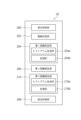
- FIG. 3 is a block diagram showing a configuration example of a control unit.
- FIG. 3 is a diagram illustrating phase difference detection.
- FIG. 3 is a diagram showing the position of a phase difference pixel on one horizontal axis of a pixel array section and a counter value.
- FIG. 3 is a diagram schematically showing an example of interfering light.
- FIG. 16 is a diagram showing an example of a histogram of a reference pixel and a histogram of a measurement pixel when not attacked in FIG. 15;
- FIG. 16 is a diagram showing a histogram of reference pixels and a histogram of measurement pixels during the attack in FIG. 15.
- FIG. 7 is a diagram showing the position of a phase difference pixel on one horizontal axis of a pixel array section and a counter value when receiving interference light.
- 5 is a timing chart showing an example of control by the comprehensive control unit.
- 5 is a flowchart showing an example of control by the comprehensive control unit.
- FIG. 2 is a schematic diagram illustrating a simplified cross section of a SPAD.
- FIG. 2 is a schematic diagram showing a cross section of a SPAD provided with an antireflection section.
- FIG. 3 is a schematic diagram in which the position of the diffusion layer is changed depending on the position of the on-chip lens or the aperture.
- FIG. 3 is a schematic diagram showing a configuration example of a pixel array section.
- FIG. 7 is a schematic diagram showing a configuration example of a pixel array section according to modification example 4 of the first embodiment.
- FIG. 3 is a diagram schematically showing an example of changing the amount of light according to a distance value using a phase difference method.
- 12 is a flowchart showing an example of control by the comprehensive control unit according to the second embodiment.
- FIG. 7 is a block diagram showing a configuration example of a control unit according to a third embodiment.
- FIG. 7 is a diagram schematically showing a processing example of a unit according to a third embodiment.
- FIG. 3 is a diagram showing a histogram corresponding to the output of each phase difference pixel generated by a histogram generation unit.
- FIG. 7 is a diagram illustrating phase difference detection according to a fourth embodiment. The figure which shows the relationship between the focal position of a pair of phase difference pixels, and an output value.
- FIG. 6 is a diagram showing the relationship between the focal position of a phase difference pixel and an output value when receiving interference light.
- 10 is a timing chart showing an example of control of a comprehensive control unit according to a fourth embodiment.
- 12 is a flowchart showing an example of control by the comprehensive control unit according to the fourth embodiment.
- FIG. 12 is a flowchart showing an example of control by the comprehensive control unit according to the fifth embodiment.
- FIG. 7 is a block diagram schematically showing an example of a schematic configuration of a ranging system according to a sixth embodiment.
- FIG. 7 is a block diagram schematically showing an example of a schematic configuration of a ranging system according to a seventh embodiment.
- FIG. 2 is a block diagram schematically showing an example of a schematic configuration of a ranging system according to a comparative example.
- FIG. 3 is a schematic cross-sectional diagram of a SPAD formed in a pixel array section.
- FIG. 3 is a diagram showing an example of a planar arrangement of phase difference pixels and measurement pixels formed in a pixel array section.
- FIG. 1 is a block diagram showing an example of a schematic configuration of a vehicle control system.
- FIG. 2 is an explanatory diagram showing an example of installation positions of an outside-vehicle information detection section and an imaging section.
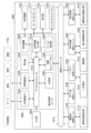
- FIG. 1 is a block diagram schematically showing an example of a schematic configuration of a ranging system 1 to which the present technology is applied.
- the distance measuring system 1 according to the first embodiment includes a light receiving device 10, a control device 22, a display device 24, an operating device 26, a lens 30 on the output side, and a lens on the input side. 40. Further, FIG. 1 further illustrates a measurement target 50. As shown in FIG.
- the light receiving device 10 includes a substrate 11, a pixel array section 12, a circuit section 13, and an infrared pulsed laser 14.
- the control unit 20 includes, for example, a CPU, and controls the light receiving device 10.
- the control device 22 is a device that controls the light receiving device 10 according to the operation of the operating device 26.
- the display device 24 is, for example, a monitor, and displays the image generated by the light receiving device 10.
- the operating device 26 includes a keyboard, a mouse, etc., and inputs an operating signal from an operator to the control device 22.
- the ranging system 1 irradiates the target object 50 with light emitted by the infrared pulsed laser 14 via the lens 30.
- the system measures the distance to the object 50 using the light reflected by the object 50 and incident on the pixel array section 12 via the lens 40. Note that details of the control section 20 will be described later.
- the pixel array section 12 is mounted on the substrate 11 and includes a plurality of measurement pixels 110i, a plurality of phase difference pixels 110z, and a plurality of reference pixels 110r.
- Each pixel of the pixel array section 12 is formed, for example, as a semiconductor element using, for example, a single photon avalanche photodiode (SPAD).
- the circuit section 13 is a circuit that controls the pixel array section 12 and performs signal processing.
- the measurement pixel 110i is a pixel used for ToF (Time of Flight), which measures the time it takes for the measurement light irradiated toward the distance measurement object to be reflected by the distance measurement object and return.
- the phase difference pixel 110z is a phase difference pixel that divides the incident light from the object 50 into pupils and detects the image plane phase difference.
- the phase difference pixel 110z is a pixel used for PDAF (Phase Detection Auto Focus).
- the phase difference pixel 110z formed using SPAD may be referred to as a PDAF pixel.
- the reference pixel 110r is used to measure the emission timing of the infrared light pulse laser 14.
- measurement using ToF may be referred to as the ToF method
- measurement using the phase difference pixel 110z may be referred to as a phase difference method.
- the infrared pulsed laser 14 is mounted on the substrate 11.
- the infrared light pulse laser 14 is formed using, for example, a VCSEL (Vertical Cavity Surface Emitting LASER) light source. Furthermore, by disposing a diffractive optical element 14a (DOE) on the irradiation side of the infrared light pulse laser 14, it is possible to irradiate the object 50 with a dot pattern of spot light arranged in a matrix of, for example, 100 points. .
- DOE diffractive optical element 14a
- the wavelength of the measurement light emitted by the infrared pulsed laser 14 is, for example, 850 [nm]. Measurement light is irradiated in synchronization with a light emission control signal input from the control unit 20.
- the reference pixel 110r within the pixel array section 12 receives pulsed light emitted by the infrared pulsed laser 14.
- pulsed light emitted by the infrared pulsed laser 14 is guided to the reference pixel 110r via a light guide member.
- the pulsed light emitted through the lens 30 enters each of the plurality of measurement pixels 110i through the lens 40 at different timings.
- the plurality of phase difference pixels 110z each receive the pulsed light emitted through the lens 30 through the lens 40.
- the plurality of phase difference pixels 110z receive pulsed light through left and right or upper and lower pairs of apertures, as described later. Thereby, the pair of phase difference pixels 110z can detect an image plane phase difference according to the distance to the object 50.
- the paired phase difference pixel 110z measures the distance to the object 50 at a different timing than the measurement using the ToF method or at a time that overlaps with the measurement using the ToF method, without using a plurality of reference pixels 110r. Measurable.
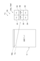
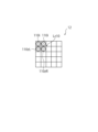
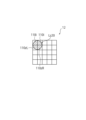
- FIG. 2 is a diagram showing a configuration example of a plurality of units 11u arranged in the pixel array section 12.
- a plurality of units 11u are arranged in a matrix.
- a reference pixel unit 166u in which the reference pixels 110r are arranged is configured at an end of the pixel array section 12.
- the unit 11u has a measurement pixel 110i made up of SPADs 331 to 334, and a phase difference pixel 110z made up of SPADs 335 and 336, respectively.
- a pixel with an aperture WL in the right half of the incident area of the SPAD 335 is defined as a phase difference pixel 110zL
- a pixel with an aperture WR in the left half of the incident area of the SPAD 336 is defined as a phase difference pixel 110zR.
- FIG. 3 is a circuit diagram showing an example of the configuration of the measurement pixel 110i.
- This measurement pixel 110i includes a quench/detection circuit 310, selection transistors 321 to 324, and SPADs 331 to 334.
- Quench/detection circuit 310 includes a resistor 311 and an inverter 312.
- pMOS p-channel Metal Oxide Semiconductor
- logic signals 309-1 to 309-4 are input from the control unit 20 to the gates of the corresponding selection transistors 21 to 324.
- SPADs Single Photon Avalanche photodiodes 331 to 334 photoelectrically convert photons and avalanche multiply them to generate current.
- a negative bias VRLD is applied to the anodes of the SPADs 331 to 334.
- the cathode of SPAD 331 is connected to the drain of selection transistor 321, and the cathode of SPAD 332 is connected to the drain of selection transistor 322. Further, the cathode of the SPAD 333 is connected to the drain of the selection transistor 323, and the cathode of the SPAD 334 is connected to the drain of the selection transistor 324.
- each of the selection transistors 321 to 324 are commonly connected to a common node 319. Furthermore, a selection signal XSEL1 from the control section 20 is input to the gates of the selection transistors 321 to 324 via selection lines 309-1 to 309-4. By varying the timing of the selection signal XSEL1, it is also possible to drive the SPADs 331 to 334 as individual pixels. When the selection signal XSEL1 becomes high level and the selection transistors 321 to 324 are conductive, the potentials VK_1 to VK_4 of the SPADs 331 to 334 are conducted to the common node 319.
- a resistor 311 is inserted between a node of a predetermined power supply voltage VDD and a common node 319.
- the inverter 312 generates a pulse signal TOUT based on the potential of the common node 319 and supplies it to a TDC (Time-to-Digital Converter) 170. Further, the resistor 311 lowers the potential of the common node 319 that exceeds a predetermined potential due to avalanche multiplication, thereby suppressing avalanche multiplication.
- the TDC 170 corresponds to the first conversion unit.
- the TDC 170 converts the light reception timing into a digital value based on the pulse signal TOUT.
- the circuit section 13 includes a clock circuit.
- the DC 170 uses the information of the clock circuit to convert the time difference between the reference time and the input time of the pulse signal TOUT into a digital value, using the measurement start time as the reference time.
- This TDC 170 supplies digital values to the control section 20.
- the TDC 170 can be configured for each unit 11u. Note that in the following description, the circuit configuration except for SPAD 331 to SPAD 340 is configured within the circuit section 13.
- FIG. 4 is a circuit diagram showing a configuration example of the phase difference pixel 110zL arranged on the left side of FIG. 3.
- This phase difference pixel 110zL includes a quench/detection circuit 310, a selection transistor 325, and a SPAD 335. Furthermore, the logic signal 309-5 is input to the gate of the corresponding selection transistor 325.
- a negative bias VRLD is applied to the anode of the SPAD 335.
- the cathode of SPAD 335 is connected to the drain of select transistor 325.
- the source of selection transistor 325 is connected to node 319.
- the selection signal XSEL2 from the control section 20 is input to the gate of the selection transistor 325 via the selection line 309-5.
- Inverter 312 generates a pulse signal COUT based on the potential of node 319 and supplies it to counter 172. Note that the counter 172 according to this embodiment corresponds to the second conversion section.
- the counter 172 counts the number of photons incident on the SPAD 335 based on the pulse signal COUT.
- This counter 172 counts the number of pulses of the pulse signal COUT as a value corresponding to the number of photons, and supplies the counted value to the control unit 20. In this manner, when the selection signal XSEL2 is at a high level and the selection transistor 325 is conductive, the potential of the SPAD 335 is conducted to the node 319. Further, the counter 172 can be configured for each unit 11u.
- FIG. 5 is a circuit diagram showing a configuration example of the phase difference pixel 110zR arranged on the right side of FIG. 3.
- This phase difference pixel 110zR has the same configuration as the phase difference pixel 110zL. That is, the phase difference pixel 110zR includes a quench/detection circuit 310, a selection transistor 326, and a SPAD 336. Furthermore, the logic signal 309-6 is input to the gate of the corresponding selection transistor 326.
- a negative bias VRLD is applied to the anode of the SPAD 336.
- the cathode of SPAD 336 is connected to the drain of select transistor 326.
- the source of selection transistor 326 is connected to node 319.
- the selection signal XSEL3 from the control section 20 is input to the gate of the selection transistor 326 via the selection line 309-6.
- Inverter 312 generates a pulse signal COUT based on the potential of node 319 and supplies it to counter 172.
- the counter 172 counts the number of photons incident on the SPAD 336 based on the pulse signal COUT.
- This counter 172 counts the number of pulses of the pulse signal COUT as a value corresponding to the number of photons, and supplies the counted value to the control unit 20. In this manner, when the selection signal XSEL3 is at a high level and the selection transistor 326 is conductive, the potential of the SPAD 336 is conducted to the node 319.
- FIG. 6 is a diagram showing an example of the circuit configuration of the reference pixel unit 166u.
- the reference pixel 110r also has the same configuration as the measurement pixel 110i. That is, this reference pixel 110r includes a quench/detection circuit 310, selection transistors 327 to 330, and SPADs 337 to 340.
- Quench/detection circuit 310 includes a resistor 311 and an inverter 312. Furthermore, logic signals 309-7 to 309-10 are input to the gates of corresponding selection transistors 327 to 330.
- each of the selection transistors 327 to 330 are commonly connected to the common node 319. Furthermore, a selection signal XSEL0 from the control section 20 is input to the gates of the selection transistors 327 to 330 via selection lines 309-7 to 309-10. When the selection signal XSEL0 is at a high level and the selection transistors 321 to 324 are conductive, the potentials VK_1 to VK_4 of the SPADs 337 to 340 are conducted to the common node 319.
- FIG. 7 is a schematic cross-sectional view of SPADs 331, 332, 335, and 336 formed in the pixel array section 12.
- the SPADs 331, 332, 335, and 336 correspond to two of the four pixels that constitute the phase difference pixel 110zL, the phase difference pixel 110zR, and the measurement pixel 110i, respectively (see FIG. 2).
- the SPAD 331 and the SPAD 332 have the same configuration. Further, the SPADs 333 and 334 also have the same configuration as the SPADs 331 and 332. That is, the four pixels forming the measurement pixel 110i have the same configuration.
- the phase difference pixel 110zL and the phase difference pixel 110zR are different from the measurement pixel 110ia in that they have apertures WL and WR, respectively.
- the apertures WL and WR are constituted by light shielding members and divide the incident lights L1 and L2 from the object 50 into pupils, respectively.
- the SPADs 337 to 340 also have the same configuration as the SPADs 331 and 332.
- the SPAD 331 includes an off-chip lens 1110, an N well 1112, a diffusion layer 1114, a metal wiring 1116, a metal pad 1118, and an inter-pixel isolation section 1120. Note that detailed description of the wiring layer is omitted. Note that the SPADs 331 to 340 can have a general configuration and are not limited to the configuration shown in FIG. 7.
- the off-chip lens 1110 focuses the light incident through the lens 40 into the N-well 1112.
- the N-well 1112 is formed by controlling the impurity concentration of the sensor substrate to be n-type, and forms an electric field that transfers electrons generated by photoelectric conversion in the SPAD to the avalanche multiplication region.
- the op-chip lens 1110 may be made of, for example, a high refractive material.
- amorphous silicon, SiN, etc. can be used as the high refractive material.
- the sensitivity to infrared light is improved, the count rate of the phase difference pixel 110zL, the phase difference pixel 110zR, and the measurement pixel 110i is improved, and the phase difference pixel 110zL and the phase difference pixel 110zR are improved. Improves light collection efficiency.
- the diffusion layer 1114 is composed of a P-type diffusion layer, an N-type diffusion layer, a hole accumulation layer, a pinning layer, and a high concentration P-type diffusion layer.
- an avalanche multiplication region is formed by a depletion layer formed in a region where a P-type diffusion layer and an N-type diffusion layer are connected.
- the metal wiring 1116 is formed wider than the diffusion layer 1114 so as to cover, for example, the avalanche multiplication region.
- the metal pad 1118 is used for electrically and mechanically bonding the metal pads formed in the logic side wiring layer to the metal (Cu) forming each pad.
- the inter-pixel isolation section 1120 insulates and isolates each SPAD by a double structure of a metal film and an insulating film formed between adjacent SPADs.
- FIG. 8 is a diagram showing an example of the arrangement of the TDC 170 and the counter 172 arranged on the substrate 11.
- the TDC 170 includes a TDC 170a arranged at the left end of the pixel array section 12 and a TDC 170b arranged at the right end of the pixel array section 12.
- the counter 172 includes a counter 172 a placed at the left end of the pixel array section 12 and a counter 172 b placed at the right end of the pixel array section 12 .
- the circuit section 13 includes, for example, two TDCs 170 and two counters 172.
- the TDC 170a is wired to a plurality of units 11u in the left half of the pixel array section 12, and the TDC 170b is wired to a plurality of units 11u in the right half of the pixel array section 12.
- the counter 172a is wired to a plurality of units 11u in the left half of the pixel array section 12, and the counter 172b is wired to a plurality of units 11u in the right half of the pixel array section 12. This allows the amount of wiring to be shortened.
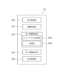
- FIG. 9 is a block diagram showing an example of the configuration of the control section 20.
- the control section 20 includes a light emission control section 200, a drive control section 202, a first distance measurement section 204, a second distance measurement section 206, and a comprehensive control section 208.
- the first distance measurement section 204 includes a histogram generation section 204a and a processing section 204b.
- the light emission control unit 200 controls the irradiation timing of the pulsed light of the dot pattern formed via the diffractive optical element 14a by supplying a light emission control signal to the infrared pulsed laser 14.
- the frequency of the light emission control signal is, for example, 20 [MHz].
- the frequency of the light emission control signal is not limited to 20 [MHz], and may be 5 [MHz] or the like.
- the light emission control signal is not limited to a rectangular wave as long as it is a periodic signal.
- the light emission control signal may be a sine wave.
- pulsed light is irradiated several times at 20 [MHz] before measurement using the ToF method. Note that the irradiation period and period are just examples, and are not limited thereto.
- FIG. 10 is a diagram schematically showing a state in which the dot pattern pulsed light reaches the light receiving surface of the pixel array section 12 as return light from the target object 50. As shown in FIG. 10, the dot pattern pulsed light is dispersed, for example, for each unit 11u and received as spot light 11s.
- the drive control unit 202 generates selection signals XSEL0 to 3 for the selection transistors 321 to 330 (see FIGS. 3 to 5), logic signals 309-1 to 309-10, etc., and controls the drive of each unit 11u and unit 116u. .
- the first distance measurement unit 204 includes a histogram generation unit 204a and a processing unit 204b.
- the histogram generation unit 204a generates a histogram based on the digital values obtained by the TDC 170.
- the processing unit 204b performs various processes based on the histogram generated by the histogram generation unit 204a. For example, the processing unit 204b can perform FIR (Finite Impulse Response) filter processing, echo determination, depth value (distance value) calculation processing, peak detection processing, and the like.
- the distance image (depth image) generated by the processing unit 204b is output via the interface.
- FIG. 11 is a diagram schematically showing a processing example of the TDC 170 of the unit 11u.
- SPADs 331-334 are connected to TDC 170
- SPADs 335 and 336 are each connected to counter 172.
- the horizontal axis of the TDC histogram shows time, and the vertical axis shows frequency.
- An example is schematically shown in which photons ph1 to ph7 are incident on each of SPADs 331 to 334 in time series.
- the unit 11u generates a pulse signal TOUT according to the photons ph1 to ph7.
- the TDC 170 generates a digital value proportional to the difference between the reference time t0 and the input timing of the pulse signal TOUT generated in time series due to the photons ph1 to ph7, and supplies it to the histogram generation unit 204a.
- the histogram generation unit 204a adds, for example, 1 to the frequency of the time interval corresponding to the digital value.
- the frequency of time intervals corresponding to digital values according to the distance to the target portion 50 increases.
- photons p are introduced into the SPADs 337 to 340 of the unit 116u in time series from the infrared pulsed laser 14.
- Unit 116u generates a pulse signal TOUT in response to the photons.
- the TDC 170 generates a digital value proportional to the difference between the input timing of the pulse signal TOUT generated in time series due to photons and the reference time t0, and supplies it to the histogram generation unit 204a.
- the frequency of time intervals corresponding to digital values according to the irradiation timing of the pulsed light increases.
- the processing unit 204b generates, for example, the time corresponding to the maximum frequency of the histogram generated by the histogram generation unit 204a for the reference pixel 110r of the unit 166u as time t1.
- the time t1 has a value approximately equal to the irradiation start time of the pulsed light.
- the processing unit 204b generates, for example, a time t2n corresponding to the maximum frequency of the histogram generated by the histogram generation unit 204a for each of the plurality of measurement pixels 110i. n indicates each unit 11u. Thereby, the processing unit 204b generates the distance Dn to the object 50 detected by each unit 11u as (t2n-t1) ⁇ speed of light/2.
- FIG. 12 is a diagram schematically showing a visible image 110a and a ranging image 110b.
- Each density point Cp of the distance measurement image 110b has a density value corresponding to the distance Dn calculated by the processing unit 204b.
- the processing unit 204b can generate a two-dimensional distance value distribution based on the pulse signal TOUT measured by each unit 11u as the distance measurement image (depth image) 110b. For example, this distance measurement image 110b is displayed on the display device 24 via the control device 22.
- FIG. 13 is a diagram illustrating phase difference detection according to the embodiment of the present disclosure.
- a in the figure is a diagram showing the relationship between the surface positions of the object 50, the lens 40, and the pixel array section 12, and the optical path of the incident light.
- light passing through the left and right sides of the lens 40 is represented by 301 and 302, respectively.
- the left, center, and right diagrams of A are on the opposite side from (the imaging surface of) the pixel array section 12 (in the focused state) when they are on (the imaging surface of) the pixel array section 12, respectively. (a so-called rear focus state) and a case on the side of the pixel array section 12 (a so-called front focus state).
- the optical images 303 and 304 have shifted shapes. This image shift represents the phase difference.
- the optical images 303 and 304 become images shifted to the left and right, respectively.
- the optical images 303 and 304 become images shifted in opposite directions.
- FIG. 14 is a diagram showing the positions and counter values of the phase difference pixels 110zL and 110zR on one horizontal axis of the pixel array section 12.
- the horizontal axis corresponds to the positions of the phase difference pixel 110zL and the phase difference pixel 110zR.
- the vertical axis is the count value of the counter 172. That is, the signal value L20 corresponds to the number of photons based on the pulse signal TOUT of the phase difference pixel 110zL. On the other hand, the signal value R20 corresponds to the number of photons based on the pulse signal TOUT of the phase difference pixel 110zR.
- the phase difference corresponds to the shift amount that minimizes the sum of the difference values between the signal value L20 and the signal value R20 when the signal value L20 or the signal value R20 is shifted in the horizontal direction.
- the second distance measuring section 206 calculates the shift amount based on the pulse signal TOUT of each unit 11u. Then, the second distance measuring unit 206 calculates the distance to the target object 50 based on the shift amount. Since the shift amount corresponds to the distance to the object 50, the distance can be measured although the accuracy is lower than that of the TOF method. In this way, in this embodiment, by using the SPADs 335 and 336, it is possible to measure the distance to the object 50 using the amount of light at the photon level.
- the second distance measuring unit 206 calculates the shift amount that minimizes the sum of the difference values between the signal value L20 and the signal value R20. The influence on light is suppressed more than the TOF method.
- FIG. 15 is a diagram schematically showing an example of interfering light.
- Fig. A schematically shows a state in which no attack has been made
- Fig. B schematically shows a state in which an attack is being received by intentional interference light.
- the attack circuit 1000 emits pulsed light having a wavelength band equivalent to that of the pulsed light to the object 50.
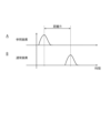
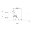
- FIG. 16 is a diagram showing an example of the histogram of the reference pixel 110r and the histogram of the measurement pixel 110i when not attacked in FIG. 15.
- Figure A shows a histogram generated by the histogram generation unit 204a based on the output signal of the reference pixel 110r
- Figure B shows a histogram generated by the histogram generation unit 204a based on the output signal of the measurement pixel 110i.
- the time difference between the peak time of the histogram of the reference pixel and the peak time of the histogram of the measurement pixel corresponds to the true distance R to the object 50.
- FIG. 17 is a diagram showing a histogram of the reference pixel 110r and a histogram of the measurement pixel 110i during the attack in FIG. 15.
- Figure A shows a histogram generated by the histogram generation unit 204a based on the output signal of the reference pixel 110r
- Figure B shows a histogram generated by the histogram generation unit 204a based on the output signal of the measurement pixel 110i.
- the histogram of the measurement pixel includes the pulse signal DOUT caused by the interfering light, and the peak of the histogram of the measurement pixel is shifted.
- the time difference between the peak time of the histogram of the reference pixel and the peak time of the histogram of the measurement pixel corresponds to the distance Rf to the false object 50f.
- the TOF method since the incident timing of photons is converted into a digital value, an erroneous signal is generated depending on the incident timing of the pulsed light of the attack circuit 1000, and the position of the object 50 is changed, for example, to the object 50f. The position may be incorrectly measured.
- the measurement accuracy with the TOF method is higher than the measurement accuracy with the phase difference method, but it is more susceptible to the influence of attack light or environmental light.
- FIG. 18 is a diagram showing the positions and counter values of the phase difference pixels 110zL and 110zR on the horizontal axis of the pixel array section 12 when receiving interference light.
- the horizontal axis corresponds to the positions of the phase difference pixel 110zL and the phase difference pixel 110zR.
- the vertical axis is the count value of the counter 172. That is, the signal value L20a corresponds to the number of photons based on the pulse signal TOUT of the phase difference pixel 110zL. On the other hand, the signal value R20a corresponds to the number of photons based on the pulse signal TOUT of the phase difference pixel 110zR.
- the phase difference corresponds to a shift amount that minimizes the sum of the difference values between the signal value L20a and the signal value R20a when the signal value L20a or the signal value R20a is shifted in the horizontal direction.
- the counter values of the phase difference pixel 110zL and the phase difference pixel 110zR only increase as the count value due to photons caused by the interference light increases as an offset. Therefore, even if interference light is received, the influence on the shift amount is suppressed.
- the signal value L20a and the signal value R20a increase by the same amount. Therefore, the influence on the shift amount is suppressed, and the influence of the pulsed light of the attack circuit 1000 and the ambient light is suppressed.
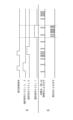
- FIG. 19 is a timing chart showing an example of control by the comprehensive control unit 208.
- the horizontal axis indicates time.
- the vertical axis in Figure A indicates the light emission control signal generated by the light emission control unit 200, the selection signal XSEL2, the selection signal XSEL3, the selection signal XSEL0, and the selection signal show. A high level of these signals indicates a driving state.
- Figure B schematically shows photons incident on the pixel array section 12. That is, photons generated by attack light or environmental light and photons generated by second measurement light are schematically shown.
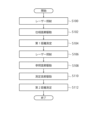
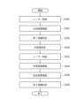
- FIG. 20 is a flowchart showing an example of control by the comprehensive control unit 208.
- a control example of the comprehensive control unit 208 will be described with reference to FIG. 19.
- the general control unit 208 sets the light emission control signal to a first high level signal for measuring the phase difference signal, and causes the infrared light pulse laser 14 to emit measurement pulse light (step S100).
- the general control unit 208 sets the selection signal XSEL2 and the selection signal
- the pixel 110zL and the phase difference pixel 110zR are driven to measure a phase difference signal (step S102).
- the range of the first measurement period in which the selection signal XSEL2 and the selection signal XSEL3 are set to high level can be set according to a predetermined measurement distance range to the target object 50.
- the second distance measurement unit 206 calculates the shift amount based on the pulse signal COUT of the phase difference pixels 110zL and zR for each unit 11u, and generates each first distance to the target object 50 (step S104). .
- distance values based on the phase difference method are generated while suppressing the effects of attack light, environmental light, and the like.
- the comprehensive control unit 208 controls the period during which the second light emission control signal is set at high level and the period during which the selection signal XSEL0 is set at high level, based on the first distance generated by the second distance measuring unit 206. . As a result, a second measurement pulse is emitted (step S106).
- the general control unit 208 sets the selection signal XSEL0 that drives the reference pixel 110r to a high level in accordance with the timing at which the second measurement pulse is emitted, and measures the signal of the reference light (step S108).
- the combination control unit 208 sets the selection signal XSEL1 that drives the measurement pixel 110i to a high level in accordance with the timing at which the second measurement pulse is emitted, and measures the measurement light signal (step S110).
- the comprehensive control unit 208 sets the measurement time range of photons reflected and returned from the object 50 to the second measurement period corresponding to the first distance value based on the phase difference method.
- the histogram generation unit 204a of the first distance measurement unit 204 adds, for example, 1 to the frequency of the time interval corresponding to the digital value, every time a digital value is input while the selection signal XSEL0 is at a high level. Then, a histogram is generated according to the output of the reference pixel 110r.
- the processing unit 204b generates, for example, a time corresponding to the maximum frequency of the histogram generated for the reference pixel 110r by the histogram generation unit 204a as time t1.
- the histogram generation unit 204a of the second distance measurement unit 206 adds, for example, 1 to the frequency of the time interval corresponding to the digital value, every time a digital value is input while the selection signal XSEL1 is at a high level. Then, a histogram corresponding to each of the plurality of measurement pixels 110i is generated. Then, the processing unit 204b generates, for example, a time t2n, a time corresponding to the maximum frequency of the histogram generated by the histogram generation unit 204a for each of the plurality of measurement pixels 110i. Thereby, the processing unit 204b generates the distance Dn to the object 50 detected by each unit 11u as (t2n-t1) ⁇ speed of light/2 (step S112).
- the comprehensive control unit 208 sets the second measurement period of photons reflected and returned from the object 50 in correspondence with the first distance value based on the phase difference method.
- photons caused by attack light or environmental light also enter the pixel array section 12 during the second measurement period in which the measurement pixel 110i is driven.
- the attack light that is incident during the measurement period is, for example, incident at high density outside the second measurement period, and photons are incident randomly due to the environmental light.
- the density of photons caused by the measurement light incident during the second measurement period increases around the time corresponding to the position of the target object 50. Therefore, the peak of the histogram generated by the histogram generation unit 204a is dominated by the influence of photons caused by the measurement light.
- the measurement accuracy of the TOF method is higher than that of the phase method when there is no attack light, so even when there is attack light, it is possible to obtain a measured distance value with higher measurement accuracy than the phase method. becomes possible.
- the comprehensive control unit 208 corresponds the second measurement period of photons reflected and returned from the target object 50 to the first distance value based on the phase difference method. I decided to set it up.
- the second measurement period is set by the first distance value that suppresses the influence of attack light or environmental light, so the influence of attack light or environmental light outside the second measurement period in the TOF method is suppressed, Deterioration in distance measurement by the TOF method in the presence of attack light is suppressed.
- the distance measuring system 1 according to the first modification of the first embodiment differs from the first embodiment in that anti-reflection sections (moth eyes) 1122 are provided in the SPADs 331, 332, 335, and 336 formed in the pixel array section 12.
- the distance measuring system 1 is different from the distance measuring system 1 according to the present invention. Below, differences from the ranging system 1 of the first embodiment will be explained.
- FIG. 21A is a simplified schematic diagram of a cross section of the SPAD. As shown in FIG. 21A, the N-well 1112 absorbs almost all visible light. On the other hand, about half of the infrared light is reflected. Therefore, in the SPAD according to the present embodiment, an antireflection portion (moth eye) 1122 is provided.
- an antireflection portion (moth eye) 1122 is provided.
- FIG. 21B is a schematic diagram showing a cross section of SPADs 331, 332, 335, and 336 provided with an antireflection portion (moth eye) 1122.
- SPADs 331, 332, 335, and 336 according to Modification 1 of the first embodiment have an antireflection structure with minute protrusions, a so-called moth-eye structure, on the surface (plate surface) on the side where light enters. has.
- the antireflection section 1122 not only prevents reflection, but also increases the effective optical path length by diffraction. In this way, an antireflection portion (moth eye) 1122, which is an uneven structure portion arranged at a predetermined pitch on the surface of the photoelectric conversion element side, is formed.
- the SPADs 333 and 334 also have the same configuration as the SPADs 331 and 332.
- the light entering the SPADs 331, 332, 335, 336 is caused to go back and forth between the N-well 1112 and the SPADs 331, 332, 335, 336 by the anti-reflection part (moth eye) 1122. sensitivity can be improved.
- FIG. 22 is a schematic diagram showing a cross section of SPADs 331, 332, 335, and 336 in which the position of the diffusion layer 1114 is changed depending on the position of the on-chip lens 1110 and the aperture WL or WR.
- the SPAD 335 by arranging the diffusion layer 1114 on the side without the aperture WL, it is possible to further increase the sensitivity.
- the SPAD 336 by arranging the diffusion layer 1114 on the side without the aperture WR, it is possible to further increase the sensitivity.
- each SPAD 331 and 332 varies depending on the arrangement position on the pixel array section 12 and the relationship with the optical axis of the lens 40. Therefore, in the SPADs 331 and 332 according to this modification, the diffusion layer 1114 is arranged in accordance with the focal position of the on-chip lens 1110. That is, the diffusion layer 1114 is arranged in alignment with the main optical axis of the chip lens 1110. This has the effect of so-called pupil correction, and it is possible to increase the sensitivity of the SPADs 331 and 332. Note that the SPADs 333 and 334 also have the same configuration as the SPADs 331 and 332.
- the distance measuring system 1 according to the third modification of the first embodiment is different from the distance measuring system 1 according to the first embodiment in that the circuit section 13 formed in the pixel array section 12 is laminated in two layers. .
- differences from the ranging system 1 of the first embodiment will be explained.
- FIG. 23 is a schematic diagram showing an example of the configuration of the pixel array section 12.
- a pixel array section 12 is configured on the first substrate 11a, and an inverter 312 for each pixel 110r, 110i, 110zR, and 110zL, TDCs 170a, b, and counters 172a, b are configured on the second substrate 11b. and place.
- the upper surface area of the light receiving device 10 can be reduced, and the light receiving device 10 can be further miniaturized.
- the distance measurement system 1 according to the fourth modification of the first embodiment is different from the distance measurement system 1 according to the first embodiment in that the circuit section 13 formed in the pixel array section 12 is laminated in three layers. .
- differences from the ranging system 1 of the first embodiment will be explained.
- FIG. 24 is a schematic diagram showing a configuration example of the pixel array section 12 according to Modification 4 of the first embodiment.
- the pixel array section 12 is configured on the first substrate 11c
- the inverter 312 for each pixel 110r, 110i, 110zR, and 110zL is configured on the second substrate 11d
- the third substrate 11e includes: A TDC 170 and a counter 172 are arranged.
- a TDC 170 corresponding to each unit 11u of the pixel array section 12 is arranged directly below each unit 11u.
- a counter 172 corresponding to each unit 11u of the pixel array section 12 is arranged directly below each unit 11u.
- the distance measurement system 1 according to the second embodiment is capable of further changing the light intensity of the measurement light used for TOF measurement based on the first distance value generated by the second distance measurement unit 206 using the phase difference method. , is different from the ranging system 1 according to the first embodiment. Below, differences from the ranging system 1 of the first embodiment will be explained.
- FIG. 25 is a diagram schematically showing an example of changing the amount of light according to the distance value using the phase difference method.
- Diagram A in FIG. 25 is an example of a short distance
- diagram B is an example of a long distance, which is farther than diagram A.
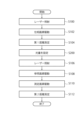
- FIG. 26 is a flowchart showing an example of control by the comprehensive control unit 208 according to the second embodiment. This flowchart is different from the flowchart showing a control example of the comprehensive control unit 208 according to the second embodiment shown in FIG. 20 in that the light amount of the infrared pulsed laser 14 is set in step S200.
- the comprehensive control unit 208 sets the light intensity of the external light pulse laser 14 according to the first distance value generated by the second distance measurement unit 206 using the phase difference method.
- the general control unit 208 stores, for example, a table that associates distance values with light amounts, and sets the light amount with reference to the table.
- the comprehensive control unit 208 adjusts the second measurement period of photons reflected and returned from the object 50 and the light intensity of the pulsed laser 14 to the first distance value using the phase difference method. I decided to configure it accordingly.
- the second measurement period is set using the first distance value that suppresses the influence of attack light or environmental light, and distance fluctuations in the amount of photons reflected from the object 50 and returned can be suppressed, so the TOF Deterioration in measurement accuracy in the method is further suppressed.
- phase difference pixels 110zL and 110zR according to the ranging system 1 of the first embodiment generate output values as count values by the counter 172
- the phase difference pixels 110zL and 110zR according to the ranging system 1 according to the third embodiment generate output values as count values.
- the pixels 110zL and 110zR are different from the ranging system 1 according to the first embodiment in that they output output values to the TDC 170 and generate count values using the TDC 170. Below, differences from the ranging system 1 of the first embodiment will be explained.
- FIG. 27 is a block diagram showing a configuration example of the control section 20 according to the third embodiment.
- the control unit 20 according to the third embodiment further includes a third distance measurement unit 210.
- the third distance measuring section 210 includes a histogram generating section 210a and a processing section 210b. Details of the processing by the third distance measuring section 210 will be described later.
- FIG. 28 is a diagram schematically showing a processing example of the unit 11u according to the third embodiment.
- the SPADs 331 to 334 are connected to the TDC 170
- the SPADs 335 and 336 according to the third embodiment are different from the SPADs 335 and 336 according to the first embodiment in that they are respectively connected to the TDC 170. differ.
- phase difference pixel 110zL having the SPAD 335 and the phase difference pixel 110zR having the SPAD 336 of the unit 11u generates a pulse signal TOUT according to these photons ph8 to ph10.
- the TDC 170 corresponding to the SPAD 335 generates a digital value proportional to the difference between the input timing of the pulse signal TOUT generated in time series due to the photons ph8 to ph9 and the reference time t0, and generates a digital value in the histogram generation section 210a. supply to.
- the TDC 170 corresponding to the PAD 336 generates a digital value proportional to the difference between the input timing of the pulse signal TOUT generated in time series due to the photons ph10 to ph11 and the reference time t0, and generates a digital value in the histogram generation section. 210a.
- the histogram generation unit 210a adds, for example, 1 to the frequency of the time interval corresponding to the digital value.
- the frequency of time intervals corresponding to digital values according to the distance to the target portion 50 increases.
- FIG. 29 is a diagram showing a histogram corresponding to the output of each of the phase difference pixels 110zL and 110zR generated by the histogram generation unit 210a.
- Figure A is a histogram corresponding to the phase difference pixel 110zL
- Figure B is a histogram corresponding to the phase difference pixel 110zR.
- the processing unit 210b generates, as a counter value, an integrated value obtained by integrating the histograms generated by the histogram generating unit 210a, for example.
- the integrated value is proportional to the number of photons that reach each of the phase difference pixels 110zL and 110zR.
- the processing unit 210b integrates the number of pulse signals TOUT generated by the TDC 170 to generate a counter value.
- this processing unit 210b calculates the shift amount based on the counter values corresponding to each of the phase difference pixels 110zL and 110zR arranged in a column. The processing unit 210b then calculates the distance to the target object 50 based on the shift amount. Since the shift amount corresponds to the distance to the object 50, the accuracy is lower than that of the TOF method, but the distance can be measured while suppressing the influence of attack light and environmental light.
- the SPADs 335 and 336 are connected to the TDC 170, and the third distance measuring section 210 generates a counter value by integrating the number of pulse signals TOUT generated by the TDC 170, We decided to calculate the distance value.
- the ranging system 1 can be configured only with the TDC 170.
- the distance measurement system 1 according to the first embodiment measures the distance using the measurement pixel 110i after measuring the distance using the phase difference pixels 110zL and 110zR, whereas the distance measurement system 1 according to the fourth embodiment measures the distance using the measurement pixel 110i.
- differences from the ranging system 1 of the first embodiment will be explained.
- FIG. 30 is a diagram illustrating phase difference detection according to the fourth embodiment.
- a in the figure is a diagram showing the relationship between the surface positions of the object 50, the lens 40, and the pixel array section 12, and the optical path of the incident light.
- light passing through the left and right sides of the lens 40 is represented by 301 and 302, respectively.
- the lights 301 and 302 that pass through the end of the lens 40 are described. Due to the on-chip lens 1110 (see FIG. 7), light 301 actually passes through the right side of the on-chip lens 1110, and light 302 actually passes through the left side of the on-chip lens 1110. Therefore, the position of the shielding part WR is schematically shown on the opposite side from FIG.
- the ⁇ (minus) position in the figure indicates a so-called rear focus state where the focal position is on the side opposite to (the imaging surface of) the pixel array section 12. Further, the 0 position in the figure indicates a focused state. Furthermore, the + (plus) position in the figure indicates a so-called front focus state in which the focal position is on the (imaging surface of) the pixel array section 12.
- FIG. 31 is a diagram showing the relationship between the focal position and the output value of the paired phase difference pixels 110zL and 110zR.
- the focus position is 0
- the - position is the rear focus state
- the + position is the front focus state.
- the output value of the phase difference pixel 110zL is assumed to be L20a
- the output value of the phase difference pixel 110zR is assumed to be R20a. That is, the output value L20a is the count value of the counter 172 corresponding to the phase difference pixel 110zL. Similarly, the output value R20a is the count value of the counter 172 corresponding to the phase difference pixel 110zR. As shown in FIG. 31, the values of L20a and R20a change depending on the degree of the rear focus state and the front focus state.
- the second distance measurement unit 206 sets the output value of the phase difference pixel 110zL of each unit 11u to L20a, sets the output value of the phase difference pixel 110zR to R20a, and based on the output values L20a and R20a, A difference value D20 is calculated. Then, the second distance measuring section 206 calculates the distance to the target object 50 for each unit 11 based on the difference value D20. Since the difference value D20 corresponds to the distance to the object 50, it is possible to measure the distance, although the accuracy is lower than with the TOF method. In this manner, in this embodiment, by using the ASPADs 335 and 336, it is possible to measure the distance to the object 50 for each unit 11u using the amount of light at the photon level.
- FIG. 32 is a diagram showing the relationship between the focal position of the phase difference pixels 110zL and 110zR and the output value when receiving interference light.
- the focus position is 0
- the - position is the rear focus state
- the + position is the front focus state.
- the output value of the phase difference pixel 110zL is assumed to be L20a
- the output value of the phase difference pixel 110zR is assumed to be R20a. That is, the output value L20a is the count value of the counter 172 corresponding to the phase difference pixel 110zL. Similarly, the output value R20a is the count value of the counter 172 corresponding to the phase difference pixel 110zR.
- the counter values of the phase difference pixel 110zL and the phase difference pixel 110zR only increase in offset due to the number of photons caused by the interference light. Therefore, even if interference light is received, the influence on the difference value D20 is suppressed. In this way, in the phase difference method using the phase difference pixel 110zL and the phase difference pixel 110zR, even if the object 50 is irradiated with the pulsed light of the attack circuit 1000, the signal value L20a and the signal value R20a increase by the same amount. Therefore, the influence of pulsed light of the attack circuit 1000, environmental light, etc. is suppressed.
- FIG. 33 is a timing chart showing an example of control by the comprehensive control unit 208 according to the fourth embodiment.
- the horizontal axis indicates time.
- the vertical axis in Figure A indicates the light emission control signal generated by the light emission control unit 200, the selection signal XSEL2, the selection signal XSEL3, the selection signal XSEL0, and the selection signal show. A high level of these signals indicates a driving state.
- Figure B schematically shows photons incident on the pixel array section 12. That is, photons generated by attack light or environmental light and photons generated by second measurement light are schematically shown.
- FIG. 34 is a flowchart showing an example of control by the comprehensive control unit 208 according to the fourth embodiment.
- a control example of the comprehensive control unit 208 according to the fourth embodiment will be described with reference to FIG. 33.
- the general control unit 208 sets the light emission control signal to a high level signal and causes the infrared light pulse laser 14 to emit measurement pulse light (step S300).
- the general control unit 208 sets the phase difference pixel 110zL and the selection signal XSEL2 and the selection signal , the phase difference pixel 110zR is driven, and the phase difference signal is measured for each unit u (step S302).
- the range in which the selection signal XSEL2 and the selection signal XSEL3 are set to high level can be set according to a predetermined measurement distance range to the target object 50.
- the second distance measuring section 206 calculates a difference value D20 for each unit 11u based on the pulse signal COUT of each unit 11u, and generates a first distance value for each unit 11u to the target object 50 (step S304). As described above, the distance value is generated while suppressing the influence of attack light and the like.
- the general control unit 208 sets the selection signal XSEL0 that drives the reference pixel 110r to a high level in accordance with the timing at which the measurement pulse is emitted, and measures the signal of the reference light (step S306).
- the histogram generation unit 204a of the first distance measurement unit 204 adds, for example, 1 to the frequency of the time interval corresponding to the digital value, every time a digital value is input while the selection signal XSEL0 is at a high level.
- a histogram is generated according to the output of the reference pixel 110r.
- the processing unit 204b generates, for example, a time corresponding to the maximum frequency of the histogram generated for the reference pixel 110r by the histogram generation unit 204a as time t1.
- the general control unit 208 sets the selection signal XSEL1 that drives each measurement pixel 110i to a high level according to the timing at which the measurement pulse is emitted, and measures the measurement light signal (step S308).
- the histogram generation unit 204a of the first distance measurement unit 204 adds, for example, 1 to the frequency of the time interval corresponding to the digital value, every time a digital value is input while the selection signal XSEL1 is at a high level. Then, a histogram corresponding to each of the plurality of measurement pixels 110i is generated.
- the processing unit 204b generates, for example, a time t2n, a time corresponding to the maximum frequency of the histogram generated by the histogram generation unit 204a for each of the plurality of measurement pixels 110i. Thereby, the processing unit 204b generates the distance Dn to the object 50 detected by each unit 11u as (t2n-t1) ⁇ speed of light/2 (step S310).
- the distance measurement values of the phase difference pixels 110zL and 110zR have lower measurement accuracy than the measurement pixel 110i, the influence of attack light and environmental light is suppressed. on the other hand.
- the distance measurement value of the measurement pixel 110i has a higher measurement accuracy than the distance measurement values of the phase difference pixels 110zL and 110zR, and tends to be easily influenced by attack light and environmental light.
- the comprehensive control unit 208 selects the distance measurement value of the measurement pixel 110i.
- the distance measurement value of the measurement pixel 110i and the distance measurement value of the phase difference pixels 110zL and 110zR are not within the predetermined range, the distance measurement value of the phase difference pixels 110zL and 110zR is selected (step S312).
- the range of the predetermined value is set to be 90% or more and 110% of the distance measurement values of the phase difference pixels 110zL and 110zR.
- distance measurements are performed in parallel by the phase difference pixels 110zL and 110zR of each unit u11 and the measurement pixel 110i, and the second distance measurement based on the first distance value of each unit u11 is performed in parallel.
- the first distance value of the phase difference pixels 110zL and 110zR is selected, and when receiving no interfering light, etc., the first distance value of the measurement pixel 110i is selected.
- FIG. 35 is a flowchart showing an example of control by the comprehensive control unit 208 according to the fifth embodiment. As shown in FIG. 35, the comprehensive control unit 208 performs (step S300) to (step S304) in the same manner as in FIG.
- the general control unit 208 sets the selection signal XSEL0 during the period in which the second light emission control signal is set to high level, and sets the selection signal XSEL1 for each unit 11u to high level according to the first distance value for each unit 11u.
- a second measurement period is set (step S400).
- the general control unit 208 sets the selection signal XSEL0 that drives the reference pixel 110r to a high level in accordance with the timing at which the second measurement pulse is emitted, and measures the signal of the reference light (step S404).
- the histogram generation unit 204a of the first distance measurement unit 204 adds, for example, 1 to the frequency of the time interval corresponding to the digital value, every time a digital value is input while the selection signal XSEL0 is at a high level.
- a histogram is generated according to the output of the reference pixel 110r.
- the processing unit 204b generates, for example, a time corresponding to the maximum frequency of the histogram generated for the reference pixel 110r by the histogram generation unit 204a as time t1.
- the general control unit 208 sets the selection signal XSEL1 that drives each measurement pixel 110i to a high level in accordance with the second measurement period of each measurement pixel 110i in accordance with the timing at which the second measurement pulse is emitted.
- the measurement light signal is measured (step S406).
- the comprehensive control unit 208 sets the range of measurement time of photons reflected and returned from the target object 50 for each unit 11u into the second measurement period corresponding to the first distance value for each unit 11u using the phase difference method. Set to .
- the histogram generation unit 204a of the first distance measurement unit 204 adds, for example, 1 to the frequency of the time interval corresponding to the digital value, every time a digital value is input while the selection signal XSEL0 is at a high level. Then, a histogram is generated for each unit 11u according to the output of the reference pixel 110r.
- the processing unit 204b generates, for example, a time corresponding to the maximum frequency of each histogram generated by the histogram generation unit 204a for the reference pixel 110r as time t1.
- the processing unit 204b generates, for example, time t2n, a time corresponding to the maximum frequency of the histogram generated by the histogram generation unit 204a for each of the plurality of measurement pixels 110i. Thereby, the processing unit 204b generates the distance Dn to the object 50 detected by each unit 11u as (t2n-t1) ⁇ speed of light/2 (step S408).
- the comprehensive control unit 208 determines the measurement period of photons reflected and returned from the object 50 for each unit 11u measured by the phase difference method. 1 distance value, and is set for each unit 11u.
- the second measurement period for each unit 11u is set based on the first distance value for each unit 11u in which the influence of attack light or environmental light is suppressed, so attack light outside the second measurement period in the TOF method Alternatively, the influence of environmental light is suppressed, and a decrease in measurement accuracy in the TOF method for each unit 11u is suppressed.
- the distance measurement system 1 according to the sixth embodiment differs from the distance measurement system 1 according to the first embodiment in that it further includes an infrared pulsed laser 16 for the phase difference pixels 110zL and 110zR. Below, differences from the ranging system 1 of the first embodiment will be explained.
- FIG. 36 is a block diagram schematically showing an example of a schematic configuration of a ranging system 1 according to the sixth embodiment.
- the ranging system 1 according to the sixth embodiment differs from the first embodiment in that it further includes an infrared pulsed laser 16 and a diffractive optical element 16a (DOE) for the phase difference pixels 110zL and 110zR. This is different from the distance measuring system 1 according to the configuration.
- DOE diffractive optical element 16a
- the infrared pulsed laser 16 is mounted on the substrate 11.
- the infrared light pulse laser 16 is formed using, for example, a VCSEL (Vertical Cavity Surface Emitting LASER) light source. Furthermore, by arranging a diffractive optical element 16a (DOE) on the irradiation side of the infrared light pulse laser 16, it is possible to irradiate the object 50 with a dot pattern of spot light arranged in a matrix of, for example, 100 points. .
- DOE diffractive optical element 16a
- the infrared pulsed laser 16 for the phase difference pixels 110zL and 110zR is further provided. This allows measurement for the phase difference pixels 110zL and 110zR and measurement for the measurement pixel 110i to be performed using independent light sources.
- the distance measurement system 1 according to the seventh embodiment differs from the distance measurement system 1 according to the first embodiment in that the phase difference pixels 110zL and 110zR, the reference pixel 110r, and the measurement pixel 110i are configured as different chips. Below, differences from the ranging system 1 of the first embodiment will be explained.
- FIG. 37A is a block diagram schematically showing a schematic configuration example of the ranging system 1 according to the seventh embodiment.
- the ranging system 1 according to the seventh embodiment includes phase difference pixels 110zL and 110zR, a reference pixel 110r, and a measurement pixel 110i as different chips.
- FIG. 37B is a block diagram schematically showing an example of a schematic configuration of a distance measuring system 1 according to a comparative example.
- the chips of the phase difference pixels 110zL and 110zR are arranged between the chip of the reference pixel 110r and the infrared light pulse laser 14. Therefore, in the comparative example, stray light from the infrared pulsed laser 14 tends to enter the chips of the phase difference pixels 110zL and 110zR.
- the infrared pulsed laser 14 is disposed between the chip of the reference pixel 110r and the chips of the phase difference pixels 110zL and 110zR, so that stray light is suppressed. Ru.
- the phase difference pixels 110zL and 110zR, the reference pixel 110r, and the measurement pixel 110i are configured as different chips. This makes it easy to differentiate the circuit configurations of the phase difference pixels 110zL and 110zR, the reference pixel 110r, and the measurement pixel 110i, further improving the degree of freedom in design.
- the ranging system 1 according to the eighth embodiment differs from the ranging system 1 according to the first embodiment in that phase difference pixels 110zL, 110zR, and reference pixel 110r are each configured for each SPAD. Below, differences from the ranging system 1 of the first embodiment will be explained.
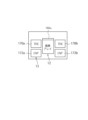
- FIG. 38 is a diagram showing a configuration example of a plurality of phase difference pixels 110zL, 110zR and a plurality of measurement pixels 110i arranged in the pixel array section 12 according to the eighth embodiment.
- each of the plurality of phase difference pixels 110zL, 110zR and the plurality of reference measurement pixels 110i is composed of one SPAD.
- Apertures WL and WR are configured in the middle between the phase difference pixels 110zL and 110zR.
- the distance measurement system 1 according to the ninth embodiment is different from the distance measurement system 1 according to the first embodiment in that the phase difference pixels 110zL and 110zR are configured with one chip, and the measurement pixel 110i is configured with another chip. differ. Below, differences from the ranging system 1 of the first embodiment will be explained.
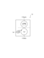
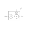
- the semiconductor element chip 110zch includes phase difference pixels 110zL and 110zR, and the semiconductor element chip 110ich includes a measurement pixel 110i. Although each chip is schematically shown as a circle, the pixels within each chip are arranged in a rectangular matrix.
- FIG. 39 is a diagram showing an example of an inverted L-shaped structure in which the chips 110zch and 110ich are arranged vertically and the infrared light pulse laser 14 is brought closer to the chip 110ich. In such a configuration, stray light from the infrared pulsed laser 14 to the phase difference pixels 110zL and 110zR is suppressed.
- FIG. 40 is a diagram showing an example of a diagonal L-shaped structure in which the chips 110zch and 110ich are arranged diagonally and the infrared light pulse laser 14 is brought closer to the chip 110ich. In such a configuration, stray light from the infrared pulsed laser 14 to the phase difference pixels 110zL and 110zR is suppressed.
- FIG. 41 is a diagram showing an example of an L-shaped structure in which the chips 110zch and 110ich are arranged horizontally and the infrared light pulse laser 14 is brought closer to the chip 110ich. In such a configuration, stray light from the infrared pulsed laser 14 to the phase difference pixels 110zL and 110zR is suppressed. Note that the inverted L-shaped structure and the diagonal L-shaped structure according to this embodiment also correspond to the L-shaped structure.
- the chip 110zch where the phase difference pixels 110zL and 110zR are arranged and the chip 110ich where the measurement pixel 110i is arranged are independently configured, and the external light pulse laser 14 is arranged on the chip 110ich.
- the distance measuring system 1 according to the tenth embodiment is different from the first to ninth embodiments in that the phase difference pixels 110zL and 110zR are configured with CIS (CMOS Image Sensor), and distance measurement can be performed using visible light. This is different from system 1. Below, differences from the ranging system 1 of the first embodiment will be explained.
- phase difference pixels 110zL and 110zR are performed by irradiating the infrared pulsed laser 14 or the infrared pulsed laser 16.
- a CIS CMOS Image Sensor
- measurement using the phase difference pixels 110zL and 110zR becomes possible without irradiation with pulsed laser light.
- a visible light source can be placed in place of the infrared pulsed laser 16. This allows measurement using the phase difference pixels 110zL and 110zR even in environments with low light intensity, such as at night.
- FIG. 42 is a schematic cross-sectional diagram of the SPADs 3310, 3320, CIS 3350, and 3360 formed in the pixel array section 12.
- the SPADs 3310, 3320, CIS 3350, and 3360 correspond to two of the four pixels forming the phase difference pixel 110zL, the phase difference pixel 110zR, and the measurement pixel 110i, respectively (see FIG. 2).
- the SPADs 3310 and 3320 differ from the SPADs 331 and 332 shown in FIG. 7 in that they each include a red filter 1122R and a blue filter 1122B. This suppresses visible light from entering the N-well 1112.
- the CIS 3350 and 3360 are configured with a green filter 1122G, and the photoelectric conversion unit 1112a is configured with a CIS (CMOS Image Sensor).
- CMOS Image Sensor CMOS Image Sensor
- the distance measuring system 1 according to the eleventh embodiment differs from the distance measuring system 1 according to the first to tenth embodiments in that the phase difference pixels 110zL and 110zR are configured with elliptical or circular on-chip lenses. Below, the differences from the first to tenth distance measuring systems 1 will be explained.
- the apertures WL and WR constitute the phase difference pixels 110zL and 110zR, but in the ranging system 1 according to the eleventh embodiment, the phase difference pixels 110zL and 110zR consists of an elliptical or circular on-chip lens.
- FIG. 43 is a diagram showing an example of the planar arrangement of the phase difference pixels 110zL, 110zR and the measurement pixel 110i formed in the pixel array section 12.
- Each pixel is composed of one SPAD.
- An elliptical on-chip lens Lz10 is arranged in the phase difference pixels 110zL and 110zR.
- FIG. 44 is a simplified cross-sectional schematic diagram of the phase difference pixels 110zL and 110zR.
- the elliptical on-chip lens Lz10 allows pupil division of the phase difference pixels 110zL and 110zR. Since no aperture is used, sensitivity can be further improved.
- FIG. 45 is a diagram showing an example of the planar arrangement of the phase difference pixels 110zL, 110zR and the measurement pixel 110i formed in the pixel array section 12.
- Each pixel is composed of one SPAD.
- a circular on-chip lens Lz20 is arranged in the phase difference pixels 110zL and 110zR and the two measurement pixels 110i. Thereby, by integrating the outputs of each SPAD in which the on-chip lens Lz20 is arranged, it is possible to configure one pixel.
- phase difference pixels 110zL and 110zR by using the outputs of the phase difference pixels 110zL and 110zR, it is possible to configure the phase difference pixels 110zL and 110zR that can perform pupil division. Pupil division of the phase difference pixels 110zL and 110zR is possible. Since no aperture is used, sensitivity can be further improved.
- the technology according to the present disclosure can be applied to various products.
- the technology according to the present disclosure can be applied to any type of transportation such as a car, an electric vehicle, a hybrid electric vehicle, a motorcycle, a bicycle, a personal mobility vehicle, an airplane, a drone, a ship, a robot, a construction machine, an agricultural machine (tractor), etc. It may also be realized as a device mounted on the body.
- FIG. 46 is a block diagram showing a schematic configuration example of a vehicle control system 7000, which is an example of a mobile object control system to which the technology according to the present disclosure can be applied.
- Vehicle control system 7000 includes multiple electronic control units connected via communication network 7010.
- the vehicle control system 7000 includes a drive system control unit 7100, a body system control unit 7200, a battery control unit 7300, an outside vehicle information detection unit 7400, an inside vehicle information detection unit 7500, and an integrated control unit 7600.
- the communication network 7010 connecting these plurality of control units is, for example, CAN (Controller Area Network), LIN (Local Interconnect Network), LAN (Local Area Network), or FlexRay. Compliant with arbitrary standards such as y (registered trademark) It may be an in-vehicle communication network.
- Each control unit includes a microcomputer that performs calculation processing according to various programs, a storage unit that stores programs executed by the microcomputer or parameters used in various calculations, and a drive circuit that drives various devices to be controlled. Equipped with Each control unit is equipped with a network I/F for communicating with other control units via the communication network 7010, and also communicates with devices or sensors inside and outside the vehicle through wired or wireless communication. A communication I/F is provided for communication. In FIG.
- the functional configuration of the integrated control unit 7600 includes a microcomputer 7610, a general-purpose communication I/F 7620, a dedicated communication I/F 7630, a positioning section 7640, a beacon receiving section 7650, an in-vehicle device I/F 7660, an audio image output section 7670, An in-vehicle network I/F 7680 and a storage unit 7690 are illustrated.
- the other control units similarly include a microcomputer, a communication I/F, a storage section, and the like.
- the drive system control unit 7100 controls the operation of devices related to the drive system of the vehicle according to various programs.
- the drive system control unit 7100 includes a drive force generation device such as an internal combustion engine or a drive motor that generates drive force for the vehicle, a drive force transmission mechanism that transmits the drive force to wheels, and a drive force transmission mechanism that controls the steering angle of the vehicle. It functions as a control device for a steering mechanism to adjust and a braking device to generate braking force for the vehicle.
- the drive system control unit 7100 may have a function as a control device such as ABS (Antilock Brake System) or ESC (Electronic Stability Control).
- a vehicle state detection section 7110 is connected to the drive system control unit 7100.
- the vehicle state detection unit 7110 includes, for example, a gyro sensor that detects the angular velocity of the axial rotation movement of the vehicle body, an acceleration sensor that detects the acceleration of the vehicle, or an operation amount of an accelerator pedal, an operation amount of a brake pedal, or a steering wheel. At least one sensor for detecting angle, engine rotational speed, wheel rotational speed, etc. is included.
- the drive system control unit 7100 performs arithmetic processing using signals input from the vehicle state detection section 7110, and controls the internal combustion engine, the drive motor, the electric power steering device, the brake device, and the like.
- the body system control unit 7200 controls the operations of various devices installed in the vehicle body according to various programs.
- the body system control unit 7200 functions as a keyless entry system, a smart key system, a power window device, or a control device for various lamps such as a headlamp, a back lamp, a brake lamp, a turn signal, or a fog lamp.
- radio waves transmitted from a portable device that replaces a key or signals from various switches may be input to the body control unit 7200.
- the body system control unit 7200 receives input of these radio waves or signals, and controls the door lock device, power window device, lamp, etc. of the vehicle.
- the battery control unit 7300 controls the secondary battery 7310, which is a power supply source for the drive motor, according to various programs. For example, information such as battery temperature, battery output voltage, or remaining battery capacity is input to the battery control unit 7300 from a battery device including a secondary battery 7310. The battery control unit 7300 performs arithmetic processing using these signals, and controls the temperature adjustment of the secondary battery 7310 or the cooling device provided in the battery device.
- the external information detection unit 7400 detects information external to the vehicle in which the vehicle control system 7000 is mounted.
- an imaging section 7410 and an external information detection section 7420 is connected to the vehicle exterior information detection unit 7400.
- the imaging unit 7410 includes at least one of a ToF (Time of Flight) camera, a stereo camera, a monocular camera, an infrared camera, and other cameras.
- the vehicle external information detection unit 7420 includes, for example, an environmental sensor for detecting the current weather or weather, or a sensor for detecting other vehicles, obstacles, pedestrians, etc. around the vehicle equipped with the vehicle control system 7000. At least one of the surrounding information detection sensors is included.
- the environmental sensor may be, for example, at least one of a raindrop sensor that detects rainy weather, a fog sensor that detects fog, a sunlight sensor that detects the degree of sunlight, and a snow sensor that detects snowfall.
- the surrounding information detection sensor may be at least one of an ultrasonic sensor, a radar device, and a LIDAR (Light Detection and Ranging, Laser Imaging Detection and Ranging) device.
- the imaging section 7410 and the vehicle external information detection section 7420 may be provided as independent sensors or devices, or may be provided as a device in which a plurality of sensors or devices are integrated.
- FIG. 47 shows an example of the installation positions of the imaging section 7410 and the vehicle external information detection section 7420.
- the imaging units 7910, 7912, 7914, 7916, and 7918 are provided, for example, at at least one of the front nose, side mirrors, rear bumper, back door, and upper part of the windshield inside the vehicle 7900.
- An imaging unit 7910 provided in the front nose and an imaging unit 7918 provided above the windshield inside the vehicle mainly acquire images in front of the vehicle 7900.
- Imaging units 7912 and 7914 provided in the side mirrors mainly capture images of the sides of the vehicle 7900.
- An imaging unit 7916 provided in the rear bumper or back door mainly acquires images of the rear of the vehicle 7900.
- the imaging unit 7918 provided above the windshield inside the vehicle is mainly used to detect preceding vehicles, pedestrians, obstacles, traffic lights, traffic signs, lanes, and the like.
- FIG. 47 shows an example of the imaging range of each of the imaging units 7910, 7912, 7914, and 7916.
- Imaging range a indicates the imaging range of imaging unit 7910 provided on the front nose
- imaging ranges b and c indicate imaging ranges of imaging units 7912 and 7914 provided on the side mirrors, respectively
- imaging range d is The imaging range of an imaging unit 7916 provided in the rear bumper or back door is shown. For example, by superimposing image data captured by imaging units 7910, 7912, 7914, and 7916, an overhead image of vehicle 7900 viewed from above can be obtained.
- the external information detection units 7920, 7922, 7924, 7926, 7928, and 7930 provided at the front, rear, sides, corners, and the upper part of the windshield inside the vehicle 7900 may be, for example, ultrasonic sensors or radar devices.
- External information detection units 7920, 7926, and 7930 provided on the front nose, rear bumper, back door, and upper part of the windshield inside the vehicle 7900 may be, for example, LIDAR devices.
- These external information detection units 7920 to 7930 are mainly used to detect preceding vehicles, pedestrians, obstacles, and the like.
- the vehicle exterior information detection unit 7400 causes the imaging unit 7410 to capture an image of the exterior of the vehicle, and receives the captured image data. Further, the vehicle exterior information detection unit 7400 receives detection information from the vehicle exterior information detection section 7420 to which it is connected.
- the external information detection unit 7420 is an ultrasonic sensor, a radar device, or a LIDAR device
- the external information detection unit 7400 transmits ultrasonic waves, electromagnetic waves, etc., and receives information on the received reflected waves.
- the external information detection unit 7400 may perform object detection processing such as a person, car, obstacle, sign, or text on the road surface or distance detection processing based on the received information.
- the external information detection unit 7400 may perform environment recognition processing to recognize rain, fog, road surface conditions, etc. based on the received information.
- the vehicle exterior information detection unit 7400 may calculate the distance to the object outside the vehicle based on the received information.
- the outside-vehicle information detection unit 7400 may perform image recognition processing or distance detection processing for recognizing people, cars, obstacles, signs, characters on the road, etc., based on the received image data.
- the outside-vehicle information detection unit 7400 performs processing such as distortion correction or alignment on the received image data, and also synthesizes image data captured by different imaging units 7410 to generate an overhead image or a panoramic image. Good too.
- the outside-vehicle information detection unit 7400 may perform viewpoint conversion processing using image data captured by different imaging units 7410.
- the in-vehicle information detection unit 7500 detects in-vehicle information.
- a driver condition detection section 7510 that detects the condition of the driver is connected to the in-vehicle information detection unit 7500.
- the driver state detection unit 7510 may include a camera that images the driver, a biosensor that detects biometric information of the driver, a microphone that collects audio inside the vehicle, or the like.
- the biosensor is provided, for example, on a seat surface or a steering wheel, and detects biometric information of a passenger sitting on a seat or a driver holding a steering wheel.
- the in-vehicle information detection unit 7500 may calculate the degree of fatigue or concentration of the driver based on the detection information input from the driver state detection unit 7510, or determine whether the driver is dozing off. You may.
- the in-vehicle information detection unit 7500 may perform processing such as noise canceling processing on the collected audio signal.
- the integrated control unit 7600 controls overall operations within the vehicle control system 7000 according to various programs.
- An input section 7800 is connected to the integrated control unit 7600.
- the input unit 7800 is realized by, for example, a device such as a touch panel, a button, a microphone, a switch, or a lever that can be inputted by the passenger.
- the integrated control unit 7600 may be input with data obtained by voice recognition of voice input through a microphone.
- the input unit 7800 may be, for example, a remote control device using infrared rays or other radio waves, or an externally connected device such as a mobile phone or a PDA (Personal Digital Assistant) that is compatible with the operation of the vehicle control system 7000. It's okay.
- the input unit 7800 may be, for example, a camera, in which case the passenger can input information using gestures. Alternatively, data obtained by detecting the movement of a wearable device worn by a passenger may be input. Further, the input section 7800 may include, for example, an input control circuit that generates an input signal based on information input by a passenger or the like using the input section 7800 described above and outputs it to the integrated control unit 7600. By operating this input unit 7800, a passenger or the like inputs various data to the vehicle control system 7000 and instructs processing operations.
- the storage unit 7690 may include a ROM (Read Only Memory) that stores various programs executed by the microcomputer, and a RAM (Random Access Memory) that stores various parameters, calculation results, sensor values, etc. Furthermore, the storage unit 7690 may be realized by a magnetic storage device such as a HDD (Hard Disc Drive), a semiconductor storage device, an optical storage device, a magneto-optical storage device, or the like.
- ROM Read Only Memory
- RAM Random Access Memory
- the storage unit 7690 may be realized by a magnetic storage device such as a HDD (Hard Disc Drive), a semiconductor storage device, an optical storage device, a magneto-optical storage device, or the like.
- the general-purpose communication I/F 7620 is a general-purpose communication I/F that mediates communication with various devices existing in the external environment 7750.
- the general-purpose communication I/F7620 supports GSM (registered trademark) (Global System of Mobile communications), WiMAX (registered trademark), LTE (registered trademark) (Long Term Evolution), or LTE-A (LTE -Advanced) and other cellular communication protocols , or other wireless communication protocols such as wireless LAN (also referred to as Wi-Fi (registered trademark)) or Bluetooth (registered trademark).
- GSM Global System of Mobile communications
- WiMAX registered trademark
- LTE registered trademark
- LTE-A Long Term Evolution
- wireless communication protocols such as wireless LAN (also referred to as Wi-Fi (registered trademark)) or Bluetooth (registered trademark).
- the general-purpose communication I/F 7620 connects to a device (for example, an application server or a control server) existing on an external network (for example, the Internet, a cloud network, or an operator-specific network) via a base station or an access point, for example. You may. Furthermore, the general-purpose communication I/F 7620 uses, for example, P2P (Peer To Peer) technology to communicate with a terminal located near the vehicle (for example, a terminal of a driver, a pedestrian, a store, or an MTC (Machine Type Communication) terminal). You can also connect it with a terminal located near the vehicle (for example, a terminal of a driver, a pedestrian, a store, or an MTC (Machine Type Communication) terminal). You can also connect it with P2P (Peer To Peer) technology to communicate with a terminal located near the vehicle (for example, a terminal of a driver, a pedestrian, a store, or an MTC (Machine Type Communication) terminal). You can also connect it with
- the dedicated communication I/F 7630 is a communication I/F that supports communication protocols developed for use in vehicles.
- the dedicated communication I/F 7630 supports, for example, WAVE (Wireless Access in Vehicle Environment), which is a combination of lower layer IEEE802.11p and upper layer IEEE1609, and DSRC (Dedicated Shore). standard protocols such as t Range Communications) or cellular communication protocols. May be implemented.
- the dedicated communication I/F 7630 is typically used for vehicle-to-vehicle communication, vehicle-to-infrastructure communication, vehicle-to-home communication, and vehicle-to-vehicle communication. to pedestrian ) communications, a concept that includes one or more of the following:
- the positioning unit 7640 receives, for example, a GNSS signal from a GNSS (Global Navigation Satellite System) satellite (for example, a GPS signal from a GPS (Global Positioning System) satellite), performs positioning, and performs positioning of the vehicle.
- GNSS Global Navigation Satellite System
- GPS Global Positioning System
- Latitude, longitude and altitude Generate location information including.
- the positioning unit 7640 may specify the current location by exchanging signals with a wireless access point, or may acquire location information from a terminal such as a mobile phone, PHS, or smartphone that has a positioning function.
- the beacon receiving unit 7650 receives, for example, radio waves or electromagnetic waves transmitted from a wireless station installed on the road, and obtains information such as the current location, traffic jams, road closures, or required travel time. Note that the function of the beacon receiving unit 7650 may be included in the dedicated communication I/F 7630 described above.
- the in-vehicle device I/F 7660 is a communication interface that mediates connections between the microcomputer 7610 and various in-vehicle devices 7760 present in the vehicle.
- the in-vehicle device I/F 7660 may establish a wireless connection using a wireless communication protocol such as wireless LAN, Bluetooth (registered trademark), NFC (Near Field Communication), or WUSB (Wireless USB).
- the in-vehicle device I/F 7660 also connects USB (Universal Serial Bus), HDMI (registered trademark) (High-Definition Multimedia Interface), or MHL (Mobile High -definition Link) etc.
- the in-vehicle device 7760 may include, for example, at least one of a mobile device or wearable device owned by a passenger, or an information device carried into or attached to the vehicle.
- the in-vehicle device 7760 may include a navigation device that searches for a route to an arbitrary destination. or exchange data signals.
- the in-vehicle network I/F 7680 is an interface that mediates communication between the microcomputer 7610 and the communication network 7010.
- the in-vehicle network I/F 7680 transmits and receives signals and the like in accordance with a predetermined protocol supported by the communication network 7010.
- the microcomputer 7610 of the integrated control unit 7600 communicates via at least one of a general-purpose communication I/F 7620, a dedicated communication I/F 7630, a positioning section 7640, a beacon reception section 7650, an in-vehicle device I/F 7660, and an in-vehicle network I/F 7680.
- the vehicle control system 7000 is controlled according to various programs based on the information obtained. For example, the microcomputer 7610 calculates a control target value for a driving force generating device, a steering mechanism, or a braking device based on acquired information inside and outside the vehicle, and outputs a control command to the drive system control unit 7100. Good too.
- the microcomputer 7610 realizes ADAS (Advanced Driver Assistance System) functions, including vehicle collision avoidance or impact mitigation, following distance based on vehicle distance, vehicle speed maintenance, vehicle collision warning, vehicle lane departure warning, etc. Coordination control may be performed for the purpose of
- the microcomputer 7610 controls the driving force generating device, steering mechanism, braking device, etc. based on the acquired information about the surroundings of the vehicle, so that the microcomputer 7610 can drive the vehicle autonomously without depending on the driver's operation. Cooperative control for the purpose of driving etc. may also be performed.
- ADAS Advanced Driver Assistance System
- the microcomputer 7610 acquires information through at least one of a general-purpose communication I/F 7620, a dedicated communication I/F 7630, a positioning section 7640, a beacon reception section 7650, an in-vehicle device I/F 7660, and an in-vehicle network I/F 7680. Based on this, three-dimensional distance information between the vehicle and surrounding objects such as structures and people may be generated, and local map information including surrounding information of the current position of the vehicle may be generated. Furthermore, the microcomputer 7610 may predict dangers such as a vehicle collision, a pedestrian approaching, or entering a closed road, based on the acquired information, and generate a warning signal.
- the warning signal may be, for example, a signal for generating a warning sound or lighting a warning lamp.
- the audio and image output unit 7670 transmits an output signal of at least one of audio and images to an output device that can visually or audibly notify information to the occupants of the vehicle or to the outside of the vehicle.
- an audio speaker 7710, a display section 7720, and an instrument panel 7730 are illustrated as output devices.
- Display unit 7720 may include, for example, at least one of an on-board display and a head-up display.
- the display section 7720 may have an AR (Augmented Reality) display function.
- the output device may be other devices other than these devices, such as headphones, a wearable device such as a glasses-type display worn by the passenger, a projector, or a lamp.
- the output device When the output device is a display device, the display device displays results obtained from various processes performed by the microcomputer 7610 or information received from other control units in various formats such as text, images, tables, graphs, etc. Show it visually. Further, when the output device is an audio output device, the audio output device converts an audio signal consisting of reproduced audio data or acoustic data into an analog signal and audibly outputs the analog signal.
- control units connected via the communication network 7010 may be integrated as one control unit.
- each control unit may be composed of a plurality of control units.
- vehicle control system 7000 may include another control unit not shown.
- some or all of the functions performed by one of the control units may be provided to another control unit.
- predetermined arithmetic processing may be performed by any one of the control units.
- sensors or devices connected to any control unit may be connected to other control units, and multiple control units may send and receive detection information to and from each other via communication network 7010. .
- a computer program for realizing each function of the ranging system 1 according to the present embodiment described using FIG. 1 can be implemented in any control unit or the like. It is also possible to provide a computer-readable recording medium in which such a computer program is stored.
- the recording medium is, for example, a magnetic disk, an optical disk, a magneto-optical disk, a flash memory, or the like.
- the above computer program may be distributed, for example, via a network, without using a recording medium.
- the light receiving device 10 of the ranging system 1 according to the present embodiment described using FIG. 1 can be applied to the imaging unit 7410 of the application example shown in FIG.
- the control section 20 can be applied to the external information detection unit 7400 shown in FIG. 46.
- the components of the ranging system 1 described using FIG. 1 are included in a module for the integrated control unit 7600 shown in FIG. May be realized.
- the ranging system 1 described using FIG. 1 may be realized by a plurality of control units of the vehicle control system 7000 shown in FIG. 46.
- a pixel array unit having a measurement pixel used to measure a distance to a target object, and a plurality of paired phase difference pixels that divide incident light from the target object into pupils and detect a phase difference; a first distance measuring unit that generates a first distance value to the target object based on information regarding a difference between a timing at which the measurement pixel receives a photon and a predetermined time; a second distance measuring unit that generates a second distance value to the object based on information corresponding to the number of photons incident on each of the plurality of phase difference pixels;
- a light receiving device comprising:
- the measurement pixel has a photoelectric conversion unit that performs photoelectric conversion according to incident photons, The light receiving device according to (1), wherein the phase difference pixel includes a photoelectric conversion section that performs photoelectric conversion according to an incident photon.
- a control unit that sets the drive period of the measurement pixel according to a first distance based on the output signals of the plurality of phase difference pixels,
- the light receiving device further comprising:
- the first distance measuring unit generates the first distance value according to a value of a histogram having appearance frequency information of a difference value between a timing at which the measurement pixel receives a photon and a predetermined time, The light receiving unit according to (1), wherein the second distance measuring unit generates the second distance value according to a phase difference using a signal value corresponding to the number of photons incident on each of the plurality of phase difference pixels.
- the measurement pixel has a plurality of the photoelectric conversion units, The measurement pixel and the plurality of paired phase difference pixels constitute a unit, further comprising a first conversion section corresponding to the unit, The light receiving device according to (5), wherein the first conversion unit generates a reception signal having information regarding a difference between a timing at which the measurement pixel receives a photon and a predetermined time.
- (10) further comprising a second conversion section corresponding to the unit, The light receiving device according to (6), wherein the second conversion unit generates a second reception signal having information corresponding to the number of photons incident on each of the plurality of phase difference pixels.
- the second conversion unit generates a third reception signal having information regarding a difference between the timing at which the phase difference pixel receives a photon and a predetermined time, and converts the second reception signal into a third reception signal according to the number of third reception signals.
- the light receiving device according to (10).
- the first chip including the measurement pixel
- the second chip including the paired phase difference pixels
- the first infrared light pulse laser are arranged in an L shape ( ).
- a pixel array section composed of a plurality of pixels; a control unit that controls the pixel array unit,
- the pixel array section includes: A plurality of phase difference pixels that form a pair that divides incident light from a target object into pupils and detects a phase difference; a measurement pixel used to measure the distance to the target object,
- the control unit is a light receiving device that sets a driving period of the measurement pixel according to a second distance based on output signals of the plurality of phase difference pixels.
- the phase difference pixel has a photoelectric conversion unit that receives visible light and performs photoelectric conversion, The light receiving device according to (15), wherein the measurement pixel includes a photoelectric conversion section that performs photoelectric conversion according to incident photons.
- the photoelectric conversion section is On-chip lens and a diffusion layer having at least an avalanche multiplication region that multiplies carriers generated by the photoelectric conversion,
- the phase difference pixel is
- the photoelectric conversion section is The aperture of the incident area, a diffusion layer having at least an avalanche multiplication region that multiplies carriers generated by the photoelectric conversion, The light receiving device according to (2), wherein the diffusion layer is arranged according to the position of the aperture.
- Two phase difference pixels among the plurality of phase difference pixels forming the pair are: The light receiving device according to (2), including an elliptical on-chip lens arranged in the photoelectric conversion section of the two phase difference pixels.
- a photoelectric conversion unit of two phase difference pixels among the plurality of paired phase difference pixels comprising a circular on-chip lens arranged in the photoelectric conversion sections of the two measurement pixels.
- the photoelectric conversion section of the phase difference pixel receives light through a color filter that transmits visible light
- a plurality of phase difference pixels that form a pair that divides incident light from a target object into pupils and detects a phase difference;
- a distance measuring system comprising: a lens that condenses incident light from the target object.
- Ranging system 10: Light receiving device, 12: Pixel array section, 14: Infrared light pulse laser, 16: Infrared light pulse laser, 20: Control section, 24: Display device, 40: Lens, 110i: Measurement Pixel, 110r: reference pixel, 110z, 110zL, 110zR: phase difference pixel, 331 to 340: SPAD, 1110: on-chip lens, 3350, 3360: CIS, Lz10, Lz20: on-chip lens, WL, WR: aperture.
Landscapes
- Engineering & Computer Science (AREA)
- Physics & Mathematics (AREA)
- Radar, Positioning & Navigation (AREA)
- Remote Sensing (AREA)
- General Physics & Mathematics (AREA)
- Computer Networks & Wireless Communication (AREA)
- Electromagnetism (AREA)
- Measurement Of Optical Distance (AREA)
- Optical Radar Systems And Details Thereof (AREA)
Abstract
Description
対象物までの距離を測定するために用いられる測定画素と、前記対象物からの入射光を瞳分割して位相差を検出する対となる複数の位相差画素と、を有する画素アレイ部と、
前記測定画素が光子を受光するタイミングと所定時点との差分に関する情報に基づき、前記対象物までの第1距離値を生成する第1距離測定部と、
前記複数の位相差画素それぞれに入射する光子の数に対応する情報に基づき、前記対象物までの第2距離値を生成する第2距離測定部と、
を備える、受光装置が提供される。
前記位相差画素は、入射した光子に応じて光電変換する光電変換部を有してもよい。
更に備えてもよい。
前記第2距離測定部は、前記複数の位相差画素それぞれに入射する光子の数に対応する信号値を用いた位相差に応じて前記第2距離値を生成してもよい。
前記測定画素と、前記対となる複数の位相差画素と、はユニットを構成しており、
前記ユニットに対応する第1変換部を更に備え、
前記第1変換部は、前記測定画素が光子を受光するタイミングと所定時点との差分に関する情報を有する受信信号を生成してもよい。
前記制御部は、前記第2距離に応じて前記第1赤外光パルスレーザが照射するレーザ光の光量を制御してもよい。
前記複数の位相差画素は、前記第2赤外光パルスレーザの照射するレーザ光に応じて信号を生成してもよい。
前記第2変換部は、前記複数の位相差画素それぞれに入射する光子の数に対応する情報を有する第2受信信号を生成してもよい。
前記測定画素が構成される第1チップと、前記対となる複数の位相差画素が構成される第2チップと、前記第1赤外光パルスレーザは、L字形状に配置されてもよい。
前記画素アレイ部を制御する制御部と、を、備え、
前記画素アレイ部は、
対象物からの入射光を瞳分割して位相差を検出する対となる複数の位相差画素と、
前記対象物までの距離を測定するために用いられる測定画素と、を有し、
前記制御部は、前記測定画素の駆動期間を、前記複数の位相差画素の出力信号に基づく、第2距離に応じて設定されてもよい。
前記測定画素は、入射した光子に応じて光電変換する光電変換部を有してもよい。
オンチップレンズと、
前記光電変換により発生したキャリアを増倍するアバランシェ増倍領域を少なくとも有する拡散層とを、有し、
前記拡散層は、前記オンチップレンズの主光軸の位置に応じて配置されてもよい。
前記光電変換部は、
入射領域の絞りと、
前記光電変換により発生したキャリアを増倍するアバランシェ増倍領域を少なくとも有する拡散層とを、有し、
前記拡散層は、前記絞りの位置に応じて配置されてもよい。
前記2つの位相差画素の光電変換部に配置される楕円形状のオンチップレンズを有してもよい。
2つの前記測定画素の光電変換部と、に配置される円形状のオンチップレンズを有してもよい。
前記測定画素の光電変換部は、赤外光を透過するカラーフィルタを介してして受光してもよい。
対象物からの入射光を瞳分割して位相差を検出する対となる複数の位相差画素と、
前記対象物までの距離を測定するために用いられる測定画素と、を有する画素アレイ部の制御方法であって、
前記測定画素の駆動期間を、前記複数の位相差画素の出力信号に基づく、第2距離に応じて設定する、制御方法が提供される。
受光装置と、
前記対象物からの入射光を集光するレンズと
を備える、測距システムが提供される。
<測距システムの構成例>
図1は、本技術を適用した測距システム1の概略構成例を模式的に示すブロック図である。図1に示すように、第1実施形態に係る測距システム1は、受光装置10と、制御装置22と、表示装置24と、操作装置26と、出射側のレンズ30と、入射側のレンズ40とを備える。また、図1では更に測定の対象物50を図示している。
図2は、画素アレイ部12に配置される複数のユニット11uの構成例を示す図である。画素アレイ部12は、複数のユニット11uが行列状に配置される。また、画素アレイ部12の端部には、参照画素110rが配置される参照画素ユニット166uが構成される。ユニット11uは、SPAD331乃至334で構成される測定画素110iと、SPAD335、336それぞれで構成される位相差画素110zとを有する。また、後述するように、SPAD335の入射領域の右半分に絞りWLのある画素を位相差画素110zLとし、SPAD336の入射領域の左半分に絞りWRのある画素を位相差画素110zRとする。
図8は、基板11上に配置されるTDC170とカウンタ172の配置例を示す図である。TDC170は、画素アレイ部12の左端部に配置されるTDC170aと、画素アレイ部12の右端部に配置されるTDC170bとを有する。同様にカウンタ172は、画素アレイ部12の左端部に配置されるカウンタ172aと、画素アレイ部12の右端部に配置されるカウンタ172bとを有する。このように、回路部13は、例えば2つのTDC170と、2つのカウンタ172を有する。
図9は、制御部20の構成例を示すブロック図である。図9に示すように、制御部20は、発光制御部200と、駆動制御部202と、第1距離測定部204と、第2距離測定部206と、総合制御部208とを有する。また、第1距離測定部204は、ヒストグラム生成部204aと、処理部204bとを有する。
図19は、総合制御部208の制御例を示すタイミングチャートである。横軸は時間を示す。A図の縦軸は、総合制御部208の制御にしたがって、発光制御部200が生成する発光制御信号、駆動制御部202が生成する選択信号XSEL2、選択信号XSEL3、選択信号XSEL0、選択信号XSEL1を示す。これらの信号は、ハイレベルが駆動状態をしめす。
第1実施形態の変形例1に係る測距システム1は、画素アレイ部12に形成されるSPAD331、332、335、336において、反射防止部(モスアイ)1122を設けた点で、第1実施形態に係る測距システム1と相違する。以下では第1実施形態の測距システム1と相違する点を説明する。
第1実施形態の変形例2に係る測距システム1は、画素アレイ部12に形成されるSPAD331、332、335、336において、拡散層1114の位置をオンチップレンズ1110、及び絞りWL、WRのいずれかの位置に応じて変更する点で、第1実施形態に係る測距システム1と相違する。以下では第1実施形態の測距システム1と相違する点を説明する。
第1実施形態の変形例3に係る測距システム1は、画素アレイ部12に形成される回路部13を2層に積層化した点で、第1実施形態に係る測距システム1と相違する。以下では第1実施形態の測距システム1と相違する点を説明する。
第1実施形態の変形例4に係る測距システム1は、画素アレイ部12に形成される回路部13を3層に積層化した点で、第1実施形態に係る測距システム1と相違する。以下では第1実施形態の測距システム1と相違する点を説明する。
第2実施形態に係る測距システム1は、第2距離測定部206が生成した位相差法による第1距離値に基づき、TOF法の測定に用いる測定光の光量を更に変更可能である点で、第1実施形態に係る測距システム1と相違する。以下では第1実施形態の測距システム1と相違する点を説明する。
第1実施形態の測距システム1に係る位相差画素110zL、110zRは、出力値をカウンタ172でカウント値として生成していたのに対し、第3実施形態に係る測距システム1に係る位相差画素110zL、110zRは、出力値をTDC170に出力し、TDC170を用いてカウント値を生成する点で、第1実施形態に係る測距システム1と相違する。以下では第1実施形態の測距システム1と相違する点を説明する。
第1実施形態の測距システム1は、位相差画素110zL、110zRによる距離測定をした後に測定画素110iによる距離測定をしていたのに対し、第4実施形態に係る測距システム1では、ユニットU11毎の位相差画素110zL、110zR、及び測定画素110iによる距離測定を並行して行う点で、第1実施形態に係る測距システム1と相違する。以下では第1実施形態の測距システム1と相違する点を説明する。
続けて、総合制御部208は、測定パルスを発光するタイミングに応じて、位相差画素110zLと、位相差画素110zRを駆動する選択信号XSEL2、及び選択信号XSEL3をハイレベルにし、位相差画素110zLと、位相差画素110zRを駆動し、位相差信号をユニットu毎に測定する(ステップS302)。選択信号XSEL2、及び選択信号XSEL3をハイレベルにする範囲は、対象物50までの予め定められている測定距離範囲に応じて設定することが可能である。
総合制御部208は、測定パルスが発光するタイミングに応じて、参照画素110rを駆動する選択信号XSEL0をハイレベルにし、参照光の信号を測定する(ステップS306)。続けて、第1距離測定部204のヒストグラム生成部204aは、選択信号XSEL0がハイレベルの期間に、デジタル値が入力される度に、そのデジタル値に応じた時間区間の頻度に例えば1を加算し、参照画素110r出力に応じたヒストグラムを生成する。処理部204bは、例えばヒストグラム生成部204aが参照画素110rに対して生成したヒストグラムの最大頻度に対応する時間を時間t1として生成する。
第4実施形態に係る測距システム1では、ユニットU11毎の位相差画素110zL、110zR、及び測定画素110iによる距離測定を並行して行っていたのに対し、第5実施形態に係る測距システム1は、ユニットU11毎に位相差画素110zL、110zRによる距離測定をした後にユニットU11毎の測定画素110iによる距離測定を行う点で、第4実施形態に係る測距システム1と相違する。以下では第5実施形態の測距システム1と相違する点を説明する。
第6実施形態に係る測距システム1では位相差画素110zL、110zR用の赤外光パルスレーザ16を、更に備える点で第1実施形態の測距システム1と相違する。以下では第1実施形態の測距システム1と相違する点を説明する。
第7実施形態に係る測距システム1では位相差画素110zL、110zRと、参照画素110r、及び測定画素110iとを異なるチップとして構成する点で第1実施形態の測距システム1と相違する。以下では第1実施形態の測距システム1と相違する点を説明する。
第8実施形態に係る測距システム1では位相差画素110zL、110zR、及び参照画素110rをそれぞれを一つのSPAD毎に構成する点で、第1実施形態の測距システム1と相違する。以下では第1実施形態の測距システム1と相違する点を説明する。
第9実施形態に係る測距システム1では位相差画素110zL、110zRを一つのチップで構成し、測定画素110iを別の一つのチップで構成する点で、第1実施形態の測距システム1と相違する。以下では第1実施形態の測距システム1と相違する点を説明する。
第10実施形態に係る測距システム1では位相差画素110zL、110zRをCIS(CMOS Image Sensor)で構成し、可視光で距離測定を可能とする点で、第1乃至第9実施形態の測距システム1と相違する。以下では第1実施形態の測距システム1と相違する点を説明する。
第11実施形態に係る測距システム1では位相差画素110zL、110zRを楕円形又は円形のオンチップレンズで構成する点で、第1乃至第10実施形態の測距システム1と相違する。以下では第1乃至第10の測距システム1と相違する点を説明する。
本開示に係る技術は、様々な製品へ応用することができる。例えば、本開示に係る技術は、自動車、電気自動車、ハイブリッド電気自動車、自動二輪車、自転車、パーソナルモビリティ、飛行機、ドローン、船舶、ロボット、建設機械、農業機械(トラクター)などのいずれかの種類の移動体に搭載される装置として実現されてもよい。
対象物までの距離を測定するために用いられる測定画素と、前記対象物からの入射光を瞳分割して位相差を検出する対となる複数の位相差画素と、を有する画素アレイ部と、
前記測定画素が光子を受光するタイミングと所定時点との差分に関する情報に基づき、前記対象物までの第1距離値を生成する第1距離測定部と、
前記複数の位相差画素それぞれに入射する光子の数に対応する情報に基づき、前記対象物までの第2距離値を生成する第2距離測定部と、
を備える、受光装置。
前記測定画素は、入射した光子に応じて光電変換する光電変換部を有し、
前記位相差画素は、入射した光子に応じて光電変換する光電変換部を有する、(1)に記載の受光装置。
前記光電変換部は、シングルフォトンアバランシェフォトダイオード(SPAD)である、(2)に記載の受光装置。
前記測定画素の駆動期間を、前記複数の位相差画素の出力信号に基づく、第1距離に応じて設定する制御部を、
更に備える、(3)に記載の受光装置。
前記第1距離測定部は、前記測定画素が光子を受光するタイミングと所定時点との差分値の出現頻度情報を有するヒストグラムの値に応じて前記第1距離値を生成し、
前記第2距離測定部は、前記複数の位相差画素それぞれに入射する光子の数に対応する信号値を用いた位相差に応じて前記第2距離値を生成する、(1)に記載の受光装置。
前記測定画素は、複数の前記光電変換部を有しており、
前記測定画素と、前記対となる複数の位相差画素と、はユニットを構成しており、
前記ユニットに対応する第1変換部を更に備え、
前記第1変換部は、前記測定画素が光子を受光するタイミングと所定時点との差分に関する情報を有する受信信号を生成する、(5)に記載の受光装置。
第1赤外光パルスレーザを更に備え、
前記制御部は、前記第2距離に応じて前記第1赤外光パルスレーザが照射するレーザ光の光量を制御する、(3)に記載の受光装置。
第2赤外光パルスレーザを更に備え、
前記複数の位相差画素は、前記第2赤外光パルスレーザの照射するレーザ光に応じて信号を生成する、(7)に記載の受光装置。
前記画素アレイ部と、前記第1変換部は積層化されており、前記ユニットに対応する前記第1変換部は、前記ユニットの直下に配置される、(6)に記載の受光装置。
前記ユニットに対応する第2変換部を更に備え、
前記第2変換部は、前記複数の位相差画素それぞれに入射する光子の数に対応する情報を有する第2受信信号を生成する、(6)に記載の受光装置。
前記第2変換部は、前記位相差画素が光子を受光するタイミングと所定時点との差分に関する情報を有する第3受信信号を生成し、第3受信信号の数に応じて前記第2受信信号を生成する、(10)に記載の受光装置。
前記測定画素と、前記対となる複数の位相差画素とは、同じ時間帯に受光した光子に応じて、信号を生成する、(11)に記載の受光装置。
前記測定画素と、前記対となる複数の位相差画素とは、異なる半導体素子のチップに構成される、(2)に記載の受光装置。
第1赤外光パルスレーザを更に備え、
前記測定画素が構成される第1チップと、前記対となる複数の位相差画素が構成される第2チップと、前記第1赤外光パルスレーザは、L字形状に配置される、(13)に記載の受光装置。
複数の画素で構成される画素アレイ部と、
前記画素アレイ部を制御する制御部と、を、備え、
前記画素アレイ部は、
対象物からの入射光を瞳分割して位相差を検出する対となる複数の位相差画素と、
前記対象物までの距離を測定するために用いられる測定画素と、を有し、
前記制御部は、前記測定画素の駆動期間を、前記複数の位相差画素の出力信号に基づく、第2距離に応じて設定する、受光装置。
前記位相差画素は、可視光を受光して光電変換する光電変換部を有し、
前記測定画素は、入射した光子に応じて光電変換する光電変換部を有する、(15)に記載の受光装置。
前記光電変換部は、入射側に反射防止部を更に有する、(2)に記載の受光装置。
前記光電変換部は、入射側に高屈折率素材で形成されたオンチップレンズを有する、(2)に記載の受光装置。
前記光電変換部は、
オンチップレンズと、
前記光電変換により発生したキャリアを増倍するアバランシェ増倍領域を少なくとも有する拡散層とを、有し、
前記拡散層は、前記オンチップレンズの主光軸の位置に応じて配置される、(2)に記載の受光装置。
前記位相差画素は、
前記光電変換部は、
入射領域の絞りと、
前記光電変換により発生したキャリアを増倍するアバランシェ増倍領域を少なくとも有する拡散層とを、有し、
前記拡散層は、前記絞りの位置に応じて配置される、(2)に記載の受光装置。
前記対となる複数の位相差画素の内の、2つの位相差画素は、
前記2つの位相差画素の光電変換部に配置される楕円形状のオンチップレンズを有する、(2)に記載の受光装置。
前記対となる複数の位相差画素の内の、2つの位相差画素の光電変換部と、
2つの前記測定画素の光電変換部と、に配置される円形状のオンチップレンズを有する、(2)に記載の受光装置。
前記位相差画素の光電変換部は、可視光を透過するカラーフィルタを介してして受光し、
前記測定画素の光電変換部は、赤外光を透過するカラーフィルタを介してして受光する、(15)に記載の受光装置。
対象物からの入射光を瞳分割して位相差を検出する対となる複数の位相差画素と、
前記対象物までの距離を測定するために用いられる測定画素と、を有する画素アレイ部の制御方法であって、
前記測定画素の駆動期間を、前記複数の位相差画素の出力信号に基づく、第2距離に応じて設定する、制御方法。
前記(1に記載の受光装置と、
前記対象物からの入射光を集光するレンズと
を備える、測距システム。
Claims (25)
- 対象物までの距離を測定するために用いられる測定画素と、前記対象物からの入射光を瞳分割して位相差を検出する対となる複数の位相差画素と、を有する画素アレイ部と、
前記測定画素が光子を受光するタイミングと所定時点との差分に関する情報に基づき、前記対象物までの第1距離値を生成する第1距離測定部と、
前記複数の位相差画素それぞれに入射する光子の数に対応する情報に基づき、前記対象物までの第2距離値を生成する第2距離測定部と、
を備える、受光装置。 - 前記測定画素は、入射した光子に応じて光電変換する光電変換部を有し、
前記位相差画素は、入射した光子に応じて光電変換する光電変換部を有する、請求項1に記載の受光装置。 - 前記光電変換部は、シングルフォトンアバランシェフォトダイオード(SPAD)である、請求項2に記載の受光装置。
- 前記測定画素の駆動期間を、前記複数の位相差画素の出力信号に基づく、第2距離に応じて設定する制御部を、
更に備える、請求項3に記載の受光装置。 - 前記第1距離測定部は、前記測定画素が光子を受光するタイミングと所定時点との差分値の出現頻度情報を有するヒストグラムの値に応じて前記第1距離値を生成し、
前記第2距離測定部は、前記複数の位相差画素それぞれに入射する光子の数に対応する信号値を用いた位相差に応じて前記第2距離値を生成する、請求項1に記載の受光装置。 - 前記測定画素は、複数の前記光電変換部を有しており、
前記測定画素と、前記対となる複数の位相差画素と、はユニットを構成しており、
前記ユニットに対応する第1変換部を更に備え、
前記第1変換部は、前記測定画素が光子を受光するタイミングと所定時点との差分に関する情報を有する受信信号を生成する、請求項2に記載の受光装置。 - 第1赤外光パルスレーザを更に備え、
前記制御部は、前記第2距離に応じて前記第1赤外光パルスレーザが照射するレーザ光の光量を制御する、請求項4に記載の受光装置。 - 第2赤外光パルスレーザを更に備え、
前記複数の位相差画素は、前記第2赤外光パルスレーザの照射するレーザ光に応じて信号を生成する、請求項7に記載の受光装置。 - 前記画素アレイ部と、前記第1変換部は積層化されており、前記ユニットに対応する前記第1変換部は、前記ユニットの直下に配置される、請求項6に記載の受光装置。
- 前記ユニットに対応する第2変換部を更に備え、
前記第2変換部は、前記複数の位相差画素それぞれに入射する光子の数に対応する情報を有する第2受信信号を生成する、請求項6に記載の受光装置。 - 前記第2変換部は、前記位相差画素が光子を受光するタイミングと所定時点との差分に関する情報を有する第3受信信号を生成し、第3受信信号の数に応じて前記第2受信信号を生成する、請求項10に記載の受光装置。
- 前記測定画素と、前記対となる複数の位相差画素とは、同じ時間帯に受光した光子に応じて、信号を生成する、請求項11に記載の受光装置。
- 前記測定画素と、前記対となる複数の位相差画素とは、異なる半導体素子のチップに構成される、請求項2に記載の受光装置。
- 第1赤外光パルスレーザを更に備え、
前記測定画素が構成される第1チップと、前記対となる複数の位相差画素が構成される第2チップと、前記第1赤外光パルスレーザは、L字形状に配置される、請求項13に記載の受光装置。 - 複数の画素で構成される画素アレイ部と、
前記画素アレイ部を制御する制御部と、を、備え、
前記画素アレイ部は、
対象物からの入射光を瞳分割して位相差を検出する対となる複数の位相差画素と、
前記対象物までの距離を測定するために用いられる測定画素と、を有し、
前記制御部は、前記測定画素の駆動期間を、前記複数の位相差画素の出力信号に基づく第2距離に応じて設定する、受光装置。 - 前記位相差画素は、可視光を受光して光電変換する光電変換部を有し、
前記測定画素は、入射した光子に応じて光電変換する光電変換部を有する、請求項15に記載の受光装置。 - 前記光電変換部は、入射側に反射防止部を更に有する、請求項2に記載の受光装置。
- 前記光電変換部は、入射側に高屈折率素材で形成されたオンチップレンズを有する、請求項2に記載の受光装置。
- 前記光電変換部は、
オンチップレンズと、
前記光電変換により発生したキャリアを増倍するアバランシェ増倍領域を少なくとも有する拡散層とを、有し、
前記拡散層は、前記オンチップレンズの主光軸の位置に応じて配置される、請求項2に記載の受光装置。 - 前記位相差画素は、
前記光電変換部は、
入射領域の絞りと、
前記光電変換により発生したキャリアを増倍するアバランシェ増倍領域を少なくとも有する拡散層とを、有し、
前記拡散層は、前記絞りの位置に応じて配置される、請求項2に記載の受光装置。 - 前記対となる複数の位相差画素の内の、2つの位相差画素は、
前記2つの位相差画素の光電変換部に配置される楕円形状のオンチップレンズを有する、請求項2に記載の受光装置。 - 前記対となる複数の位相差画素の内の、2つの位相差画素の光電変換部と、
2つの前記測定画素の光電変換部と、に配置される円形状のオンチップレンズを有する、請求項2に記載の受光装置。 - 前記位相差画素の光電変換部は、可視光を透過するカラーフィルタを介してして受光し、
前記測定画素の光電変換部は、赤外光を透過するカラーフィルタを介してして受光する、請求項15に記載の受光装置。 - 対象物からの入射光を瞳分割して位相差を検出する対となる複数の位相差画素と、
前記対象物までの距離を測定するために用いられる測定画素と、を有する画素アレイ部の制御方法であって、
前記測定画素の駆動期間を、前記複数の位相差画素の出力信号に基づく、第2距離に応じて設定する、制御方法。 - 前記請求項1に記載の受光装置と、
前記対象物からの入射光を集光するレンズと
を備える、測距システム。
Priority Applications (1)
| Application Number | Priority Date | Filing Date | Title |
|---|---|---|---|
| CN202380038147.7A CN119365792A (zh) | 2022-05-12 | 2023-05-02 | 光接收设备、控制方法及测距系统 |
Applications Claiming Priority (2)
| Application Number | Priority Date | Filing Date | Title |
|---|---|---|---|
| JP2022078931A JP2023167618A (ja) | 2022-05-12 | 2022-05-12 | 受光装置、制御方法、及び測距システム |
| JP2022-078931 | 2022-05-12 |
Publications (1)
| Publication Number | Publication Date |
|---|---|
| WO2023219045A1 true WO2023219045A1 (ja) | 2023-11-16 |
Family
ID=88730455
Family Applications (1)
| Application Number | Title | Priority Date | Filing Date |
|---|---|---|---|
| PCT/JP2023/017181 Ceased WO2023219045A1 (ja) | 2022-05-12 | 2023-05-02 | 受光装置、制御方法、及び測距システム |
Country Status (3)
| Country | Link |
|---|---|
| JP (1) | JP2023167618A (ja) |
| CN (1) | CN119365792A (ja) |
| WO (1) | WO2023219045A1 (ja) |
Citations (6)
| Publication number | Priority date | Publication date | Assignee | Title |
|---|---|---|---|---|
| JP2000346941A (ja) * | 1999-06-08 | 2000-12-15 | Mitsubishi Electric Corp | 距離測定装置 |
| US20110304842A1 (en) * | 2010-06-15 | 2011-12-15 | Ming-Tsan Kao | Time of flight system capable of increasing measurement accuracy, saving power and/or increasing motion detection rate and method thereof |
| US20160124089A1 (en) * | 2014-10-31 | 2016-05-05 | Cedes Safety & Automation Ag | Absolute distance measurement for time-of-flight sensors |
| WO2019065291A1 (ja) * | 2017-09-28 | 2019-04-04 | ソニーセミコンダクタソリューションズ株式会社 | 撮像素子および撮像装置 |
| WO2021106529A1 (ja) * | 2019-11-29 | 2021-06-03 | 富士フイルム株式会社 | 情報処理装置、情報処理方法、及びプログラム |
| JP2021148643A (ja) * | 2020-03-19 | 2021-09-27 | 株式会社リコー | 距離補正情報の算出方法、測距装置、移動体及びステレオカメラ装置 |
-
2022
- 2022-05-12 JP JP2022078931A patent/JP2023167618A/ja active Pending
-
2023
- 2023-05-02 CN CN202380038147.7A patent/CN119365792A/zh not_active Withdrawn
- 2023-05-02 WO PCT/JP2023/017181 patent/WO2023219045A1/ja not_active Ceased
Patent Citations (6)
| Publication number | Priority date | Publication date | Assignee | Title |
|---|---|---|---|---|
| JP2000346941A (ja) * | 1999-06-08 | 2000-12-15 | Mitsubishi Electric Corp | 距離測定装置 |
| US20110304842A1 (en) * | 2010-06-15 | 2011-12-15 | Ming-Tsan Kao | Time of flight system capable of increasing measurement accuracy, saving power and/or increasing motion detection rate and method thereof |
| US20160124089A1 (en) * | 2014-10-31 | 2016-05-05 | Cedes Safety & Automation Ag | Absolute distance measurement for time-of-flight sensors |
| WO2019065291A1 (ja) * | 2017-09-28 | 2019-04-04 | ソニーセミコンダクタソリューションズ株式会社 | 撮像素子および撮像装置 |
| WO2021106529A1 (ja) * | 2019-11-29 | 2021-06-03 | 富士フイルム株式会社 | 情報処理装置、情報処理方法、及びプログラム |
| JP2021148643A (ja) * | 2020-03-19 | 2021-09-27 | 株式会社リコー | 距離補正情報の算出方法、測距装置、移動体及びステレオカメラ装置 |
Also Published As
| Publication number | Publication date |
|---|---|
| CN119365792A (zh) | 2025-01-24 |
| JP2023167618A (ja) | 2023-11-24 |
Similar Documents
| Publication | Publication Date | Title |
|---|---|---|
| US12474451B2 (en) | Light reception device and distance measurement device | |
| US11743604B2 (en) | Imaging device and image processing system | |
| JP7511562B2 (ja) | 受光装置及び受光装置の制御方法、並びに、測距装置 | |
| US20230384431A1 (en) | Light receiving device and distance measuring apparatus | |
| JPWO2020022137A1 (ja) | 受光装置及び測距装置 | |
| WO2021111766A1 (ja) | 受光装置及び受光装置の制御方法、並びに、測距装置 | |
| JP2021128084A (ja) | 測距装置および測距方法 | |
| JP2023066297A (ja) | 光検出装置および測距システム | |
| WO2023067755A1 (ja) | 光検出装置、撮像装置および測距装置 | |
| US20250199129A1 (en) | Light-receiving element and electronic apparatus | |
| WO2023162734A1 (ja) | 測距装置 | |
| WO2023190278A1 (ja) | 光検出装置 | |
| US12429566B2 (en) | Photodetector, driving method of photodetector, and distance measuring device | |
| WO2021053958A1 (ja) | 受光装置、並びに、測距装置及び測距装置の制御方法 | |
| WO2024162109A1 (ja) | 光検出装置及び測距システム | |
| WO2024195531A1 (ja) | 光検出装置、及び測距システム | |
| WO2023219045A1 (ja) | 受光装置、制御方法、及び測距システム | |
| WO2023190277A1 (ja) | 光検出装置 | |
| JP2023174137A (ja) | 光検出装置 | |
| US20230106211A1 (en) | Distance measuring device and distance measuring method | |
| WO2021161858A1 (ja) | 測距装置および測距方法 | |
| WO2026083816A1 (ja) | 光検出装置 | |
| WO2025063105A1 (ja) | 発光装置及び測距装置 | |
| WO2024095625A1 (ja) | 測距装置および測距方法 | |
| WO2024057471A1 (ja) | 光電変換素子、固体撮像素子、測距システム |
Legal Events
| Date | Code | Title | Description |
|---|---|---|---|
| 121 | Ep: the epo has been informed by wipo that ep was designated in this application |
Ref document number: 23803522 Country of ref document: EP Kind code of ref document: A1 |
|
| WWE | Wipo information: entry into national phase |
Ref document number: 202380038147.7 Country of ref document: CN |
|
| NENP | Non-entry into the national phase |
Ref country code: DE |
|
| WWP | Wipo information: published in national office |
Ref document number: 202380038147.7 Country of ref document: CN |
|
| 122 | Ep: pct application non-entry in european phase |
Ref document number: 23803522 Country of ref document: EP Kind code of ref document: A1 |