WO2023218533A1 - 光回路 - Google Patents
光回路 Download PDFInfo
- Publication number
- WO2023218533A1 WO2023218533A1 PCT/JP2022/019836 JP2022019836W WO2023218533A1 WO 2023218533 A1 WO2023218533 A1 WO 2023218533A1 JP 2022019836 W JP2022019836 W JP 2022019836W WO 2023218533 A1 WO2023218533 A1 WO 2023218533A1
- Authority
- WO
- WIPO (PCT)
- Prior art keywords
- waveguide
- test
- circuit
- optical
- waveguides
- Prior art date
- Legal status (The legal status is an assumption and is not a legal conclusion. Google has not performed a legal analysis and makes no representation as to the accuracy of the status listed.)
- Ceased
Links
Images






Classifications
-
- G—PHYSICS
- G02—OPTICS
- G02F—OPTICAL DEVICES OR ARRANGEMENTS FOR THE CONTROL OF LIGHT BY MODIFICATION OF THE OPTICAL PROPERTIES OF THE MEDIA OF THE ELEMENTS INVOLVED THEREIN; NON-LINEAR OPTICS; FREQUENCY-CHANGING OF LIGHT; OPTICAL LOGIC ELEMENTS; OPTICAL ANALOGUE/DIGITAL CONVERTERS
- G02F1/00—Devices or arrangements for the control of the intensity, colour, phase, polarisation or direction of light arriving from an independent light source, e.g. switching, gating or modulating; Non-linear optics
- G02F1/01—Devices or arrangements for the control of the intensity, colour, phase, polarisation or direction of light arriving from an independent light source, e.g. switching, gating or modulating; Non-linear optics for the control of the intensity, phase, polarisation or colour
- G02F1/21—Devices or arrangements for the control of the intensity, colour, phase, polarisation or direction of light arriving from an independent light source, e.g. switching, gating or modulating; Non-linear optics for the control of the intensity, phase, polarisation or colour by interference
- G02F1/225—Devices or arrangements for the control of the intensity, colour, phase, polarisation or direction of light arriving from an independent light source, e.g. switching, gating or modulating; Non-linear optics for the control of the intensity, phase, polarisation or colour by interference in an optical waveguide structure
- G02F1/2257—Devices or arrangements for the control of the intensity, colour, phase, polarisation or direction of light arriving from an independent light source, e.g. switching, gating or modulating; Non-linear optics for the control of the intensity, phase, polarisation or colour by interference in an optical waveguide structure the optical waveguides being made of semiconducting material
-
- G—PHYSICS
- G01—MEASURING; TESTING
- G01M—TESTING STATIC OR DYNAMIC BALANCE OF MACHINES OR STRUCTURES; TESTING OF STRUCTURES OR APPARATUS, NOT OTHERWISE PROVIDED FOR
- G01M11/00—Testing of optical apparatus; Testing structures by optical methods not otherwise provided for
-
- G—PHYSICS
- G02—OPTICS
- G02B—OPTICAL ELEMENTS, SYSTEMS OR APPARATUS
- G02B6/00—Light guides; Structural details of arrangements comprising light guides and other optical elements, e.g. couplings
- G02B6/10—Light guides; Structural details of arrangements comprising light guides and other optical elements, e.g. couplings of the optical waveguide type
- G02B6/12—Light guides; Structural details of arrangements comprising light guides and other optical elements, e.g. couplings of the optical waveguide type of the integrated circuit kind
-
- G—PHYSICS
- G02—OPTICS
- G02B—OPTICAL ELEMENTS, SYSTEMS OR APPARATUS
- G02B6/00—Light guides; Structural details of arrangements comprising light guides and other optical elements, e.g. couplings
- G02B6/10—Light guides; Structural details of arrangements comprising light guides and other optical elements, e.g. couplings of the optical waveguide type
- G02B6/12—Light guides; Structural details of arrangements comprising light guides and other optical elements, e.g. couplings of the optical waveguide type of the integrated circuit kind
- G02B6/122—Basic optical elements, e.g. light-guiding paths
- G02B6/125—Bends, branchings or intersections
-
- G—PHYSICS
- G02—OPTICS
- G02F—OPTICAL DEVICES OR ARRANGEMENTS FOR THE CONTROL OF LIGHT BY MODIFICATION OF THE OPTICAL PROPERTIES OF THE MEDIA OF THE ELEMENTS INVOLVED THEREIN; NON-LINEAR OPTICS; FREQUENCY-CHANGING OF LIGHT; OPTICAL LOGIC ELEMENTS; OPTICAL ANALOGUE/DIGITAL CONVERTERS
- G02F1/00—Devices or arrangements for the control of the intensity, colour, phase, polarisation or direction of light arriving from an independent light source, e.g. switching, gating or modulating; Non-linear optics
- G02F1/01—Devices or arrangements for the control of the intensity, colour, phase, polarisation or direction of light arriving from an independent light source, e.g. switching, gating or modulating; Non-linear optics for the control of the intensity, phase, polarisation or colour
- G02F1/015—Devices or arrangements for the control of the intensity, colour, phase, polarisation or direction of light arriving from an independent light source, e.g. switching, gating or modulating; Non-linear optics for the control of the intensity, phase, polarisation or colour based on semiconductor elements having potential barriers, e.g. having a PN or PIN junction
- G02F1/0151—Devices or arrangements for the control of the intensity, colour, phase, polarisation or direction of light arriving from an independent light source, e.g. switching, gating or modulating; Non-linear optics for the control of the intensity, phase, polarisation or colour based on semiconductor elements having potential barriers, e.g. having a PN or PIN junction modulating the refractive index
- G02F1/0154—Devices or arrangements for the control of the intensity, colour, phase, polarisation or direction of light arriving from an independent light source, e.g. switching, gating or modulating; Non-linear optics for the control of the intensity, phase, polarisation or colour based on semiconductor elements having potential barriers, e.g. having a PN or PIN junction modulating the refractive index using electro-optic effects, e.g. linear electro optic [LEO], Pockels, quadratic electro optical [QEO] or Kerr effect
-
- G—PHYSICS
- G02—OPTICS
- G02F—OPTICAL DEVICES OR ARRANGEMENTS FOR THE CONTROL OF LIGHT BY MODIFICATION OF THE OPTICAL PROPERTIES OF THE MEDIA OF THE ELEMENTS INVOLVED THEREIN; NON-LINEAR OPTICS; FREQUENCY-CHANGING OF LIGHT; OPTICAL LOGIC ELEMENTS; OPTICAL ANALOGUE/DIGITAL CONVERTERS
- G02F1/00—Devices or arrangements for the control of the intensity, colour, phase, polarisation or direction of light arriving from an independent light source, e.g. switching, gating or modulating; Non-linear optics
- G02F1/01—Devices or arrangements for the control of the intensity, colour, phase, polarisation or direction of light arriving from an independent light source, e.g. switching, gating or modulating; Non-linear optics for the control of the intensity, phase, polarisation or colour
- G02F1/015—Devices or arrangements for the control of the intensity, colour, phase, polarisation or direction of light arriving from an independent light source, e.g. switching, gating or modulating; Non-linear optics for the control of the intensity, phase, polarisation or colour based on semiconductor elements having potential barriers, e.g. having a PN or PIN junction
- G02F1/025—Devices or arrangements for the control of the intensity, colour, phase, polarisation or direction of light arriving from an independent light source, e.g. switching, gating or modulating; Non-linear optics for the control of the intensity, phase, polarisation or colour based on semiconductor elements having potential barriers, e.g. having a PN or PIN junction in an optical waveguide structure
-
- G—PHYSICS
- G02—OPTICS
- G02F—OPTICAL DEVICES OR ARRANGEMENTS FOR THE CONTROL OF LIGHT BY MODIFICATION OF THE OPTICAL PROPERTIES OF THE MEDIA OF THE ELEMENTS INVOLVED THEREIN; NON-LINEAR OPTICS; FREQUENCY-CHANGING OF LIGHT; OPTICAL LOGIC ELEMENTS; OPTICAL ANALOGUE/DIGITAL CONVERTERS
- G02F1/00—Devices or arrangements for the control of the intensity, colour, phase, polarisation or direction of light arriving from an independent light source, e.g. switching, gating or modulating; Non-linear optics
- G02F1/01—Devices or arrangements for the control of the intensity, colour, phase, polarisation or direction of light arriving from an independent light source, e.g. switching, gating or modulating; Non-linear optics for the control of the intensity, phase, polarisation or colour
- G02F1/21—Devices or arrangements for the control of the intensity, colour, phase, polarisation or direction of light arriving from an independent light source, e.g. switching, gating or modulating; Non-linear optics for the control of the intensity, phase, polarisation or colour by interference
- G02F1/212—Mach-Zehnder type
-
- G—PHYSICS
- G02—OPTICS
- G02F—OPTICAL DEVICES OR ARRANGEMENTS FOR THE CONTROL OF LIGHT BY MODIFICATION OF THE OPTICAL PROPERTIES OF THE MEDIA OF THE ELEMENTS INVOLVED THEREIN; NON-LINEAR OPTICS; FREQUENCY-CHANGING OF LIGHT; OPTICAL LOGIC ELEMENTS; OPTICAL ANALOGUE/DIGITAL CONVERTERS
- G02F1/00—Devices or arrangements for the control of the intensity, colour, phase, polarisation or direction of light arriving from an independent light source, e.g. switching, gating or modulating; Non-linear optics
- G02F1/01—Devices or arrangements for the control of the intensity, colour, phase, polarisation or direction of light arriving from an independent light source, e.g. switching, gating or modulating; Non-linear optics for the control of the intensity, phase, polarisation or colour
- G02F1/21—Devices or arrangements for the control of the intensity, colour, phase, polarisation or direction of light arriving from an independent light source, e.g. switching, gating or modulating; Non-linear optics for the control of the intensity, phase, polarisation or colour by interference
- G02F1/218—Devices or arrangements for the control of the intensity, colour, phase, polarisation or direction of light arriving from an independent light source, e.g. switching, gating or modulating; Non-linear optics for the control of the intensity, phase, polarisation or colour by interference using semi-conducting materials
-
- G—PHYSICS
- G02—OPTICS
- G02F—OPTICAL DEVICES OR ARRANGEMENTS FOR THE CONTROL OF LIGHT BY MODIFICATION OF THE OPTICAL PROPERTIES OF THE MEDIA OF THE ELEMENTS INVOLVED THEREIN; NON-LINEAR OPTICS; FREQUENCY-CHANGING OF LIGHT; OPTICAL LOGIC ELEMENTS; OPTICAL ANALOGUE/DIGITAL CONVERTERS
- G02F1/00—Devices or arrangements for the control of the intensity, colour, phase, polarisation or direction of light arriving from an independent light source, e.g. switching, gating or modulating; Non-linear optics
- G02F1/01—Devices or arrangements for the control of the intensity, colour, phase, polarisation or direction of light arriving from an independent light source, e.g. switching, gating or modulating; Non-linear optics for the control of the intensity, phase, polarisation or colour
- G02F1/21—Devices or arrangements for the control of the intensity, colour, phase, polarisation or direction of light arriving from an independent light source, e.g. switching, gating or modulating; Non-linear optics for the control of the intensity, phase, polarisation or colour by interference
- G02F1/225—Devices or arrangements for the control of the intensity, colour, phase, polarisation or direction of light arriving from an independent light source, e.g. switching, gating or modulating; Non-linear optics for the control of the intensity, phase, polarisation or colour by interference in an optical waveguide structure
Definitions
- the present invention relates to silicon photonics optical circuits, and more particularly to inspection circuits for optical circuits.
- Si photonics whose core material is silicon (Si), which is widely used as a semiconductor
- Si photonics optical circuits can be significantly smaller than conventional optical circuits.
- the refractive index of Si is extremely high, compared to conventional optical circuits that have been developed based on low-refractive-index materials, the confinement of light is stronger and the waveguide can be constructed with a smaller bending radius.
- Si photonics optical circuits can realize desired functions such as optical transceivers by integrating various circuit elements.
- the Si photonics chip is packaged into an optical module, and input/output terminals for optical and electrical signals are configured.
- the optical module By incorporating the optical module into a transmission device, etc., it becomes possible to efficiently construct and operate an optical communication system.
- CMOS circuits and the like that use the same Si and have only electric circuits
- general-purpose wafer inspection technology can be used, and it is easy to select non-defective products in the wafer state.
- testing of Si photonics optical circuits is performed using both optical and electrical signals. For this reason, testing of Si photonics optical circuits is extremely complicated, leading to increased costs in terms of equipment costs and testing time, as shown in Patent Document 1.
- test circuit elements in addition to this circuit leads to an increase in chip area.
- One aspect of the present invention is an optical circuit formed on a silicon substrate, which includes a Mach-Zehnder interferometer type modulator including two arm waveguides in which a PN junction is formed in a cross section, and a test circuit for the modulator.
- an input section including a rectangular waveguide into which test light is input; a PN junction connected to the rectangular waveguide and having the same configuration as at least one of the arm waveguides in parallel with the two arm waveguides; and a test circuit including an optical branch configured with a rectangular waveguide, which branches the test light into equal intensities and propagates the two branched lights in mutually opposite directions to the test waveguide. It is an optical circuit equipped with
- the optical circuit of the present invention provides an inspection circuit that accurately reflects manufacturing errors in the circuit including the modulator and achieves miniaturization.
- FIG. 1 is a diagram showing the configuration of an optical module including a Si photonics chip.
- 1 is a diagram showing a Si photonics chip configuration including a modulator test circuit.
- FIG. FIG. 3 is a diagram showing a Si photonics chip configuration including other optical circuits of a modulator.
- 1 is a diagram showing the configuration of a general Mach-Zehnder interferometer type modulator.
- FIG. 3 is a diagram showing a cross-sectional structure of a waveguide in two arm waveguides.
- 1 is a diagram showing the configuration of a conventional inspection circuit in an optical circuit including a modulator;
- FIG. 3 is a diagram showing the configuration of another test circuit in an optical circuit including a modulator.
- FIG. 3 is a diagram illustrating a mask shift mode in a zigzag modulation waveguide.
- 1 is a diagram showing the configuration of an inspection circuit for an optical circuit according to Embodiment 1 including a modulator.
- FIG. 3 is a diagram showing the configuration of optical branching in the test circuit of Embodiment 1.
- FIG. 7 is a diagram showing the configuration of an optical circuit inspection circuit according to a second embodiment including a modulator.
- FIG. FIG. 7 is a diagram showing the configuration of an optical circuit inspection circuit of Embodiment 3 including a modulator.
- the optical circuit of the present disclosure provides a test circuit with a novel configuration that accurately reflects manufacturing errors in an optical circuit including a modulator formed on a silicon substrate.
- a test circuit is disclosed that accurately reflects the influence of manufacturing errors that occur in the modulator of this circuit during the manufacturing process of the optical circuit, and at the same time achieves miniaturization.
- the configuration of a test circuit in a conventional Si photonics chip and its problems will be explained.
- the configuration and operation of the inspection circuit in the optical circuit of the present disclosure will be explained.
- FIG. 1 is a diagram showing the configuration of an optical module including a Si photonics chip.
- the optical module 100 includes a Si photonics chip 10 including a plurality of optical modulators 11.
- the Si photonics chip 10 interfaces an electrical signal 17 with the outside through an electrical input/output wiring 15. Further, an optical fiber 13 fixed by an optical fiber assembly 12 interfaces light with the outside.
- the optical circuit in the chip 10 includes four optical modulators 11 connected in parallel to the input waveguide 14 and an output waveguide 16, but the configuration shown in FIG. 1 is only an example of the optical circuit. . It is assumed that the Si photonics chip 10 described below includes at least one optical modulator 11. In the manufacturing process of the optical module 100, inspection can be easily performed using the electrical input/output wiring 15 and the input/output interface of the optical fiber assembly 12.
- FIG. 2 is a diagram showing the configuration of a Si photonics chip including a modulator inspection circuit.
- the Si photonics chip 10 will be referred to as the Si chip 10 for simplicity.
- the Si chip 10 includes the four optical modulators 11 described in FIG. 1, and is the main circuit 10-1 that will be actually used after being mounted in an optical module.
- the Si chip 10 includes a test circuit 20 in addition to the four optical modulators (Mod) 11 of the present circuit 10-1.
- test modulator (Test Mod) 21 for the modulator is provided in the Si chip 10 as a test circuit, and this test modulator 21 is evaluated in place of the optical modulator 11 of the circuit 10-1. It becomes possible to predict the performance of this circuit.
- FIG. 3 is a diagram showing the configuration of a Si photonics chip including other optical circuits of the modulator.
- the Si photonics circuit may include an optical circuit 14 that performs other functions and may have a more complex configuration depending on its use.
- an element circuit 22 corresponding to the optical circuit 14 used in the present circuit 10-1 can be provided.
- FIGS. 2 and 3 by evaluating the Test Mod 21 and the element circuit 22 in the test circuit 20 and predicting the performance of this circuit 10-1, practical Si chip testing becomes possible. .
- the optical modulator 11 occupies a very large area.
- the Test Mod 21 in the test circuit 20 also occupies a large area.
- FIG. 4 is a diagram showing the configuration of a general Mach-Zehnder interferometer modulator.
- FIG. 4(a) shows a top view (xy plane) of a Mach-Zehnder interferometer (MZI) optical modulator fabricated on a Si substrate
- FIG. 4(b) shows a waveguide.
- a cross-sectional view (xz plane) of the portion is shown.
- the optical waveguide MZI type modulator 11 consists of two couplers 32 and 33 and two arm waveguides 35a and 35b connecting them.
- the light input to the coupler 32 on the input side is branched, propagates in the y-axis direction through two arm waveguides, and is combined by the coupler 33 on the output side.
- the two couplers 32 and 33 are also referred to as optical wiring sections 30-1 and 30-2 because they have the function of splitting/combining light and distributing the light.
- the arm waveguides 35a and 35b are configured as modulation waveguides for modulating electrical signals, and function as the modulation section 31.
- the optical waveguide MZI type modulator 11 is widely used in Si photonics, and will be simply referred to as a modulator hereinafter.
- FIG. 4(b) shows a cross section perpendicular to the length direction of each waveguide, and the modulator 11 is composed of two types of optical waveguides.
- a Y branch circuit is used as the input-side coupler 32 and the output-side coupler 33, respectively. It has the function of optical wiring to distribute light from/to the arm waveguide, and generally uses a rectangular waveguide.
- the diagram on the right side of FIG. 4(b) shows, for example, a cross section of a rectangular waveguide of the coupler 32 on the input side, and a ridge-shaped rectangular waveguide (core) 32 is placed on a substrate 50 that acts as a cladding. It is formed. Both parts of the coupler 32, which splits light into two, and the coupler 33, which combines two lights, are formed by rectangular waveguides.
- the two arm waveguides 35a and 35b are each configured as a modulation waveguide, and a special form such as a rib-type waveguide is used to convert information of an electrical signal into an optical signal.
- the diagram on the left side of FIG. 4(b) shows a cross section of the rib-type waveguide which is the arm waveguide 35a for modulation. Different impurity doping is performed with the center of the rib portion having a step structure in the x direction as a boundary, and one side is a P-type region 51 and the other side is an N-type region 52.
- the refractive index of the core is modulated.
- the refractive index modulation of the core by the electrical signal changes the phase difference between the lights propagating through the two arm waveguides, and the interference state when the lights are combined in the coupler 33 changes in accordance with the electrical signal.
- the optical modulator 11 also includes rectangular waveguide phase shifters 34a and 34b.
- a desired modulated light can be obtained by adjusting the phase modulated light in the rib waveguide of the modulation section 31 to an appropriate interference state using the phase shifters 34a and 34b.
- the arm waveguide that performs modulation in the modulation section 31 has a point where a PN junction is formed by two doped regions in the core cross section.
- the structure is significantly different from the rectangular waveguides in the waveguides 32 and 33.
- the overall length of the modulator is generally from several 100 ⁇ m to several mm depending on the design conditions. Therefore, if a modulator having the same structure as that shown in FIG. 4A is provided in a chip as a test circuit, the chip area will be significantly increased. In order to inspect optical loss in a modulator, it is important to accurately reproduce the loss in the modulation waveguide. If the characteristics of the modulator in this circuit deteriorate due to manufacturing variations as described later, it is necessary to accurately reproduce the deterioration in the test circuit.
- the loss of the modulating arm waveguide having a rib-type structure greatly affects the modulator characteristics. Therefore, when inspecting a modulator, it is important to accurately evaluate the loss of a modulation arm waveguide in which a PN junction is formed by two types of doping regions.
- FIG. 5 is a diagram showing the cross-sectional structure of the waveguide in two arm waveguides.
- FIG. 5(a) shows the cross-sectional structure when there is no mask displacement
- FIG. 5(b) shows the cross-sectional structure when the mask for generating the P-type region is displaced in the ⁇ x direction.
- the modulator 11 includes two arm waveguides 35a and 35b, and in the following explanation, in order to distinguish between the two arm waveguides, the A waveguide The right side of the waveguide is called the B waveguide.
- the arm waveguides 35a and 35b have a rib-type structure in which a silicon portion is processed into a convex step.
- the impurity is introduced so that the center position of the convex portion of the rib in the x-axis direction is the boundary position between the P-type region and the N-type region.
- impurities are implanted by ion implantation (hereinafter referred to as implantation).
- FIG. 5(a) shows an ideal state in which the mask for the implantation process does not shift and the PN junction is accurately formed at the center of the core.
- the cross-sectional structure (xz plane) of the A waveguide 35a and the B waveguide 35b is designed such that the P-type region 51 and the N-type region 52 are symmetrical. ing.
- a PN junction is formed with the center line along the length direction of each of the arm waveguides 35a and 35b as a boundary.
- the P-type region and the N-type region are arranged symmetrically with respect to the center line of the modulator 11 along the light traveling direction (y direction). That is, a symmetrical design is used both in the shape of the arm waveguide and in the arrangement of the two impurity regions. In order to suppress characteristic deterioration due to various manufacturing process variations of the two modulation waveguides of MZI, it is possible to use the above-mentioned symmetrical structure.
- Characteristic deterioration of rib-type waveguides due to manufacturing errors can occur in various ways, but one typical example is an increase in waveguide loss.
- One of the causes of increased loss is the misalignment of the respective implant positions for forming the P-type region 51 and the N-type region 52, which is independently caused by the respective mask misalignment for the P-type region and the N-type region. .
- Another factor contributing to the increase in waveguide loss is a deviation in the shape of the waveguide due to process errors in manufacturing the convex structure of the rib-type waveguide. When there is no mask shift or waveguide shape shift and the PN junction is formed symmetrically as shown in FIG. 5(a), the same loss is given to the light propagating through the two arm waveguides. Therefore, the A waveguide and the B waveguide will have the same characteristics.
- FIG. 5(b) shows a state in which the mask for the implantation process of the P-type region is misaligned due to manufacturing errors, and the PN junction is formed deviating from the ideal structure. Specifically, a case is shown in which the mask of the P-type region is shifted in the -x direction, and in the A waveguide 35a, a blank region 53 in which no impurity is introduced is formed in the center of the core. Furthermore, in the B waveguide 35b, P-type impurities are introduced overlappingly into the N-type region side beyond the core center, and the substantial impurity concentration is reduced in this overlapping region 54.
- FIG. 6 is a diagram showing the configuration of a conventional inspection circuit in an optical circuit including a modulator.
- a part of the substrate (chip) of the Si photonics circuit is shown, and the MZI modulator 11 in the main circuit and the MZI modulator 21 in the test circuit are shown.
- the A waveguide 35a and B waveguide 35b used in the modulator 11 of this circuit the A waveguide 35a and B waveguide 35b having the same length and the same PN junction structure are used in the modulator of the test circuit. 21 in the chip.
- the two arm waveguides of the present circuit and the two arm waveguides of the test circuit are arranged to be completely parallel, and that the positions in the waveguide length direction are also the same.
- the effects of misalignment of the implant position and manufacturing errors of the convex structure that occur during the manufacturing process on the modulator characteristics can be minimized. are the same.
- the performance of the modulator 11 of this circuit can be estimated.
- the size of the modulator 11 of the main circuit and the modulator 21 of the test circuit are the same, and an increase in the chip area becomes a problem. Furthermore, since it is necessary to adjust the interference state using the phase shifters 34a and 34b, a complicated inspection system using optical and electrical signals is required. Although not clearly shown in FIG. 6, the rectangular waveguides of the optical wiring sections 30-1 and 30-2 of the inspection circuit 21 extend to the end face of the Si chip and are connected to optical fibers etc. via the end face of the substrate, thereby reducing loss. will be inspected. Two fibers need to be connected to the optical measurement system.
- FIG. 7 is a diagram showing the configuration of another inspection circuit in an optical circuit including a modulator.
- the test circuit 21A on the right side of FIG. 7 differs from the modulator 21 of the test circuit shown in FIG. 6 in that it does not have the form of a modulator, but is a test circuit that estimates the performance of the A waveguide 35a of this circuit. . It has the same length as the A waveguide 35a of this circuit, and is miniaturized by the modulation waveguide 36 having a zigzag folded shape.
- the rectangular waveguides of the optical wiring sections 30-1A and 30-2A have the same length as the optical wiring sections 30-1 and 30-2 of this circuit.
- the manufacturing error of the rib shape (convex structure) in the manufacturing process is the same between the main circuit and the test circuit, and the test accuracy equivalent to that of the test modulator 21 in FIG. 6 can be obtained. It looks like that. However, when a mask shift occurs in either the P-type region or the N-type region, the amount of implant position shift and the manner of the shift are significantly different between the modulator 11 of this circuit and the inspection circuit 21A, as described below. ing.
- FIG. 8 is a diagram illustrating a mode of mask displacement in a zigzag modulation waveguide.
- FIG. 8A is the same as the test circuit 21A shown in FIG. 7, and shows three parts of the modulation waveguide 36 through which light propagates.
- the light input to the optical wiring section 30-1A constituted by a rectangular waveguide first propagates through the i portion of the modulation waveguide 36 in the +y direction. Next, the light propagates through part ii in the +x direction, and then further propagates through part iii in the -y direction.
- the modulation waveguide 36 the light changes direction in a zigzag pattern and propagates while feeling the waveguide structure. Therefore, in estimating the performance of the circuit, it is important to determine whether the waveguide structure of the test circuit that allows light to be sensed along the propagation direction accurately reflects the state of the circuit.
- FIG. 8(b) shows a waveguide structure in which light is felt in the modulation waveguide 36 folded in a zigzag shape when the mask for the P-type region is shifted in the -x direction.
- the cross-sectional structure of the waveguide of the modulation waveguide 36 of FIG. 8(a) corresponding to the A waveguide is shown in the order of the i section, the ii section, and the iii section along the propagation direction.
- each diagram in FIG. 8(b) shows a waveguide structure in which light is felt as it propagates.
- FIG. 8 shows a modulation waveguide (not shown) that has the same shape as the modulation waveguide 36 in (a) and corresponds to the B waveguide 35b of this circuit, along the propagation direction.
- the cross-sectional structure of the waveguide is shown in the order of parts, ii, and iii.
- the modulation waveguide for the B waveguide is not shown, the overall shape of the modulation waveguide 21A in FIG. 8(a) may be reversed horizontally, and the P-type region and the N-type region may also be reversed.
- FIG. 8(b) what should be noted in FIG. 8(b) is that when the cross-sectional structure of the zigzag modulation waveguide 36 is viewed along the light propagation direction, the PN junction that occurs due to mask displacement depending on the light propagation direction. are different in shape. In other words, the cross-sectional structure of the waveguide that the light perceives changes depending on the direction in which the light propagates.
- the inspection circuit 21A folded in a zigzag shape does not accurately reflect the influence caused by manufacturing errors of the modulation waveguide in this circuit, and the accuracy as an optical circuit inspection circuit is reduced.
- the performance change of the modulation waveguide caused by mask displacement differs between the main circuit and the test circuit.
- the rectangular waveguides of the optical wiring sections 30-1A and 30-2A of the inspection circuit 21 extend to the end surface of the Si chip and connect the optical fibers through the end surface of the substrate. etc., and a loss test is performed. It is necessary to optically connect two fibers at the end faces of two opposing sides of the chip.
- test circuit 21 shown in FIG. 6 has an increased chip size, whereas the test circuit 21A shown in FIG. None of them were sufficient in that they could not be done.
- test circuit 21A For optical circuits including modulators, there is a need for a test circuit that can accurately reproduce the amount of variation in characteristics due to manufacturing errors that occur in the modulator of this circuit, while at the same time realizing miniaturization.
- the optical circuit of the present disclosure provides a test circuit that accurately reflects the influence of manufacturing errors occurring in the optical modulator of the present circuit, and at the same time achieves miniaturization.
- the new test circuit described below employs a test method that uses only test light without using electrical signals, thereby simplifying the test process for MZI modulators.
- a modulator typically has electrical terminals that control the phase difference. By applying a control voltage to this electrical terminal, the phase difference is adjusted so that the loss of the entire modulator is minimized. Loss inspection is performed by inputting light into the modulator while a control voltage is applied.
- testing using electricity and light requires a complex testing system and complicated procedures. In order to simplify the inspection process, it is important to use an inspection method that uses only light for inspection.
- a modulator When a modulator is realized using an MZI type configuration including two arm waveguides as shown in FIG. 4, it is ideally designed so that the transmittances of the A waveguide 35a and the B waveguide 35b are equal.
- the above-mentioned implant position shift or process error in manufacturing the convex structure of the waveguide occurs, a difference occurs in the transmittance of the A waveguide and the B waveguide.
- the electric field transmittance of the A waveguide is t A
- the electric field transmittance of the B waveguide is t B
- the phase difference between the arm waveguides is ⁇
- the above equation expresses the principle of amplitude modulation by the MZI modulator, and by controlling this phase difference ⁇ with an electrical signal, the overall transmittance can be modulated and the modulator can be used as an optical modulator.
- the transmittances t A and t B of the A waveguide and the B waveguide can be determined individually, the overall transmittance T M as a modulator can be estimated. . Therefore, if the transmittances t A and t B of the A waveguide and the B waveguide can be measured using a highly accurate inspection circuit, the influence of manufacturing errors can be accurately grasped and reflected in the quality evaluation of the manufacturing process.
- the optical circuit of the present disclosure is equipped with a test waveguide half the length of the arm waveguide of this circuit.
- the configuration is such that light propagates in two directions on the test waveguide, achieving reproduction of the same characteristics as the modulator of this circuit.
- a loop-shaped path configured between the branch ports of the optical branch is used. Embodiments with different configurations are disclosed depending on the manner in which the two branched lights of the test light are guided to the test waveguide.
- the optical branch divides the test light with equal intensity, and after each branched light propagates along a loop-shaped path, the two branched lights are combined in the same phase.
- test circuit in the optical circuit of the present disclosure makes it possible to accurately estimate the modulator characteristics in the circuit from the test waveguide characteristics.
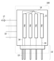
- FIG. 9 is a diagram showing the configuration of a test circuit in the optical circuit of Embodiment 1 including the modulator of the present disclosure.
- FIG. 9(a) shows the top surface (xy plane) of the test circuit 61A formed on the Si substrate of the optical circuit including the modulator.
- the optical circuit includes the main circuit 10-1 and the test circuit 20, and the test circuit 61A corresponds to Test Mod 21, which is a part of the test circuit 20.
- FIG. 9B shows a waveguide cross section (xz plane) of the test waveguide 60a, which corresponds to the modulation arm waveguide 35a of this circuit.
- the test circuit 61A includes a rectangular waveguide 37-1 (input section) into which the test light 40 is input, a test waveguide 60a connected to the rectangular waveguide 37-1, A light reflecting section is provided to reflect the test light propagating in the +y direction through the test waveguide 60 in the opposite direction (-y direction).
- the light reflecting section includes a rectangular waveguide 37-2, an optical branch 38, and a loop-shaped rectangular waveguide 39.
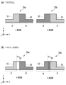
- FIG. 10 is a diagram showing the configuration of the light reflecting section in the test circuit of Embodiment 1.
- (a) of FIG. 10 shows the propagation of the test light on the outward path
- (b) shows the propagation of the test light on the return path.
- the test light 40 propagates in the y direction from the test waveguide 60a and reaches the optical branch 38.
- the optical branch divides the input light into equal parts and outputs branched lights 41a and 41b having the same intensity in two directions of the loop-shaped rectangular waveguide 39.
- the branched lights 41a and 41b propagated around the loop-shaped rectangular waveguide 39 are combined in the same phase by the optical branch 38, and the combined test light 42 is passed through the test waveguide.
- the optical branch 38 of the light reflection section branches the test light propagating on the outgoing path of the test waveguide into equal intensities, and further combines the branched lights again to propagate to the test waveguide as the return path. It works like that.
- the light reflecting section shown in FIG. 10 propagates the test light in two directions on the test waveguide 60a and operates as a loopback mirror for reciprocating the test light.
- the left diagram in (b) shows the waveguide structure of the i section where the test light traveling along the outgoing path of the test waveguide 60a in the y direction is felt, and the mask for the P-type region is shifted in the -x direction. ing. That is, since only the P-type region 51 is shifted in the -x direction, a blank region 53 into which impurities are not introduced is generated.
- the right figure in (b) shows the waveguide structure of the ii section where the test light traveling in the return path of the test waveguide 60a in the -y direction is felt, and shows the case where the mask for the P-type region is shifted in the -x direction. It shows.
- the waveguide structure felt by the test light on the outbound and return trips differs only in that the positions of the P-type region and N-type region are reversed left and right, and the profile of the PN junction caused by mask misalignment is be substantially the same. Since the outward and return paths of the physically identical test waveguide 60a are used, the test light senses a cross-sectional structure that is symmetrical with respect to the center line of the rib structure.
- the waveguide structures of the outbound path i section and the return path section ii which are felt by the test light, are the same. Therefore, the waveguide loss caused by the mask shift for the P-type region is also the same in the outgoing and returning paths.
- the consistency of the cross-sectional structure felt by the test light through the outbound and return passes is the same even if a shift occurs only in the mask in the N-type region, or even if shifts occur simultaneously and independently in both the P-type and N-type masks. .
- the length of the test waveguide 60a in the test circuit 61A is set to half (1/2) of the length of the arm waveguide 35a, which is the modulation waveguide of this circuit, the Changes in the cross-sectional structure due to mask displacement or the like can be accurately reproduced in the test waveguide 60a.
- the test light propagates substantially the same length as the arm waveguide 35a of the circuit through the outgoing and returning paths of the test waveguide 60a. Therefore, the influence of manufacturing errors that occur in the optical modulator of this circuit during the manufacturing process can be accurately reflected in the inspection circuit 61A.
- the arm waveguide 35a of this circuit and the test waveguide 60a of the test circuit 61A must be configured in parallel. Note that the length of the test waveguide 60a is not necessarily limited to half (1/2) the length of the arm waveguide 35a, which will be explained at the end.
- the present invention provides a Mach-Zehnder interferometer type modulator including two arm waveguides 35a and 35b in which a PN junction is formed in the cross section in an optical circuit formed on a silicon substrate, and a test circuit 61A for the modulator.
- an input section including a rectangular waveguide 37-1 into which the test light 40 is input; It is composed of at least one test waveguide 60a having a PN junction of the same configuration and a rectangular waveguide, splits the test light into equal intensities, and propagates the two branched lights to the test waveguide in mutually opposite directions.
- the inspection circuit including the optical branch 38 can be implemented.
- the total length of the at least one test waveguide mentioned above may be 1/2 of the length of the arm waveguide.
- the input section is a single rectangular waveguide 37-1, and at least one test waveguide is a single test waveguide 60a having a length of 1/2 of the arm waveguide.
- One end of the single test waveguide is connected to the single rectangular waveguide of the input section, and the other end of the single test waveguide is connected to the input side port of the optical branch 38.
- the branch side ports of the optical branch are connected in a loop shape by a single rectangular waveguide 39.
- the test circuit 61A shown in FIG. 9 is a test circuit for the A waveguide 35a of the circuit shown in FIG.
- a test circuit 61B for the B waveguide 35b of this circuit is obtained.
- Two test circuits corresponding to the two arm waveguides of this circuit can test the transmittance (t A , t B ) of each arm waveguide.
- inspection can be performed using only test light without using electrical signals, and a simplified measurement system with only one optical input/output fiber is required, making the inspection procedure simpler. becomes.
- the inspection system is greatly simplified compared to the conventional inspection circuit 21, which required two fibers for measurement at the end faces on two sides of the chip. Further, the round-trip transmittance of the test waveguide 60a, which is configured with half the length of the modulation waveguide 35a of the present circuit, matches the electric field transmittance of the modulation waveguide 35a of the present circuit. Therefore, by simply substituting the electric field transmittances (t A , t B ) obtained from the A waveguide test circuit and the B waveguide test circuit into equation (2), the loss of the MZI modulator of this circuit can be reduced. Estimation becomes possible.
- test circuit 61A In the test circuit 61A, a certain amount of excessive loss occurs in the rectangular waveguide 37-1 that serves as the light input/output section and in the loopback mirror that serves as the light reflection section. Therefore, it is necessary to separately calculate the excess loss using a test circuit or the like provided for the light reflecting section and compensate for the electric field transmittance of the test circuit.
- the arm waveguides 35a and 35b of the main circuit and the test waveguides 60a and B waveguide for the A waveguide of the test circuit are arranged so that there is no difference in the cross-sectional structure of the modulation waveguide between the test circuit and the main circuit.
- the waveguide test waveguides 60b are designed to be parallel to each other. As a result, even if an implant position shift or the like occurs, the characteristic fluctuation of the modulator of this circuit can be accurately estimated in the test circuit.
- the implant position etc. may be changed in the longitudinal direction in the A waveguide and the B waveguide. Even in that case, by halving the length while maintaining the longitudinal design, the characteristics of this circuit can be estimated from the test circuit as shown in FIG.
- the PN junctions of the two arm waveguides of this circuit were configured symmetrically with respect to the center line along the direction of optical propagation of the modulator.
- the structure of the PN junction in the cross section of the first arm waveguide (A waveguide) and the structure of the PN junction in the cross section of the second arm waveguide (B waveguide) are two parallel to the propagation direction of light. is symmetrical about the center line of the arm waveguide.
- a first test circuit 61A corresponding to the first arm waveguide and a second test circuit 62B corresponding to the second arm waveguide are provided. It should be noted that if the A waveguide and the B waveguide do not have a symmetrical structure but have the same structure, a single common test circuit is sufficient.
- a light reflecting section including an optical branch is provided at one end of the single test waveguide 60a, and the test light is transmitted to the single test waveguide 60a for test light.
- the outbound and return trips were realized.
- the test light i.e., the two branched lights
- the test waveguide 60a is propagating on the return path.
- the test circuit can be realized by a different configuration of the optical branches, in which the two branched lights are propagated in opposite directions to the test waveguide.
- FIG. 11 is a diagram showing the configuration of a test circuit in the optical circuit of Embodiment 2 including the modulator of the present disclosure.
- FIG. 11(a) shows the top surface (xy plane) of the test circuit 62B formed on the Si substrate of the optical circuit including the modulator.
- the optical circuit includes a main circuit 10-1 and a test circuit 10-2, and the test circuit 62B in FIG. 11 corresponds to Test Mod 21, which is a part of the test circuit 20 in FIG. .
- (b) of FIG. 11 shows the i section of the test waveguide 60-1 of the two test waveguides, which corresponds to the arm waveguide 35b (B waveguide) of this circuit, and the test waveguide 60-2.
- the cross-sectional structure (xz plane) of part ii is shown.
- the test circuit 62B has a configuration in which two test waveguides 60-1 and 60-2 are included in the loop path of the light reflecting section shown in FIG. .
- the lengths of the two test waveguides 60-1 and 60-2 in the test circuit 62B are half (1/2) of the length of the arm waveguide 35b, which is the modulation waveguide of this circuit.
- the two test waveguides 60-1 and 60-2 have the same cross-sectional structure in terms of the PN junction structure. Therefore, in the cross section of the xz plane, the P-type region and the N-type region have the same positional relationship.
- the test light 40 is input from the lowermost rectangular waveguide 37 to the input port of the optical branch 38.
- the optical branch 38 divides the test light equally, and outputs branched light of the same intensity from the branch port to two directions of the loop path including the two test waveguides.
- One branched light output from one branch port of the optical branch 38 propagates in the y direction through the test waveguide 60-1, passes through the rectangular waveguide 39-2, and then passes through the test waveguide 60-2. is propagated in the opposite direction (-y direction).
- One branched light propagates clockwise along the loop path and reaches the other branched port.
- the other branch light output from the other branch port of the optical branch 38 propagates counterclockwise along the loop path and reaches the branch port.
- the two branched lights propagating in opposite directions each pass through two test waveguides 60-1 and 60-2, and suffer loss over the entire length of the test waveguides 60-1 and 60-2. .
- the two branched lights propagated through the loop path are combined in phase and output from the rectangular waveguide 37 as test light that has passed through the test waveguides 60-1 and 60-2.
- FIG. 11(b) the cross-sectional structure of the waveguides that the test light senses in the two test waveguides 60-1 and 60-2 described above is shown.
- the left diagram in (b) shows the waveguide structure of the i section where the test light traveling through the test waveguide 60-1 in the y direction is felt, and the mask for the N-type region is shifted in the -x direction. ing. That is, since only the N-type region 51 is shifted in the ⁇ x direction, N-type impurities are introduced into the P-type region side in duplicate, resulting in an overlapping region 54.
- the figure on the right in (b) shows the waveguide structure of part ii where the test light traveling through the test waveguide 60-2 in the -y direction is felt, and shows the case where the mask for the N-type region is shifted in the -x direction. It shows.
- the waveguide structure that the test light senses in the two test waveguides 60-1 and 60-2 differs only in that the positions of the P-type region and the N-type region are reversed left and right, which is caused by mask misalignment.
- the profiles of the PN junctions are essentially the same.
- the test light traveling around the loop path will perceive a cross-sectional structure that is symmetrical about the centerline of the rib structure. In that only the N-type region crosses the center line of the rib structure and forms an overlapping region 54 with the P-type region, the waveguide structures of the i section and the ii section that the test light senses are the same.
- the waveguide loss caused by the mask shift for the N-type region is also the same.
- the consistency of the cross-sectional structure felt by the test light through the two test waveguides 60-1 and 60-2 is independent at the same time for both the P-type and N-type masks, even if only the mask in the P-type region is misaligned. The same thing applies if there is a shift.
- the input section is a single rectangular waveguide 37 connected to an optical branch 38, and the at least one test waveguide has a length of 1/2 of the arm waveguide.
- two test waveguides 60-1 and 60-2 having one end of each of the two test waveguides connected to a branch side port of the optical branch; The other end is connected by a rectangular waveguide 39-2, and the two test waveguides can be connected in a loop between the branch ports.
- the optical branch 38 operates to propagate two test lights split with equal intensity to the test waveguide.
- the optical branch 38 multiplexes two branched lights and then propagates them to the return path of a single test waveguide.
- the optical branch 38 propagates the two branched lights to the test waveguide in the loop path in opposite directions.
- Embodiment 1 and Embodiment 2 The difference between Embodiment 1 and Embodiment 2 is based on whether the test waveguide is outside the loop path or included within the loop path.
- test light travels back and forth in a single test waveguide, so that the test waveguide is reflected at different timings. Test light propagates in two directions.
- the test light propagates simultaneously in two directions on the test waveguide.
- the overall transmittance of the two test waveguides 60-1 and 60-2 in the test circuit 62B of this embodiment matches the transmittance of the arm waveguide 35b of this circuit.
- Two test circuits corresponding to the two arm waveguides of this circuit can test the transmittance (t A , t B ) of each arm waveguide.
- the MZI type modulation of this circuit can be performed as in Embodiment 1. It becomes possible to estimate the loss of the device.
- the arm waveguides 35a and 35b of the main circuit and the two test waveguides of the test circuit are arranged so that there is no difference in the cross-sectional structure of the modulation waveguide between the test circuit 62B and the main circuit.
- 60-1 and 60-2 are designed so that they are all parallel to each other. Even with the inspection circuit 62B in FIG. 11, inspection is possible by using only the test light without using electrical signals, and a simplified measurement system with only one optical input/output fiber is required, making the inspection procedure simpler. It is.
- the lengths of the two test waveguides 60-1 and 60-2 are not necessarily limited to half (1/2) of the length of the arm waveguide 35a.
- a configuration example of a test circuit is shown in which a test waveguide further divided into a large number of parts is provided in the loop path of the optical branch to further shorten the length of one test waveguide.
- the total length of the test waveguide of the test circuit is maintained at half the length of the arm waveguide of the main circuit, and is divided into a plurality of test waveguides.
- this circuit accurately reflects the influence of manufacturing errors occurring in the optical modulator, and at the same time achieves miniaturization of the test circuit.
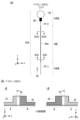
- FIG. 12 is a diagram showing the configuration of an optical circuit inspection circuit according to Embodiment 3 including the modulator of the present disclosure.
- FIG. 12(a) shows the top surface (xy plane) of the test circuit 63A formed on the Si substrate of the optical circuit including the modulator.
- the test circuit 63A in FIG. 12 corresponds to Test Mod 21, which is a part of the test circuit 20 in FIG. (b) of FIG. 12 shows the i section of the test waveguide 60-1 and the test waveguide 60-2 of the four test waveguides corresponding to the arm waveguide 35a (A waveguide) of this circuit.
- the waveguide cross-sectional structure (xz plane) of part ii is shown.
- the test circuit 63A has a configuration in which four test waveguides 60-1 to 60-4 are included in the loop path of the light reflecting section shown in FIG. .
- the length of each of the four test waveguides 60-1 to 60-4 in the test circuit 63A is set to 1/4 of the length of the arm waveguide 35a, which is the modulation waveguide of this circuit.
- the four test waveguides 60-1 to 60-4 have the same cross-sectional structure in terms of the PN junction structure. Therefore, in the cross section of the xz plane, the P-type region and the N-type region have the same positional relationship.
- the lengths of the four test waveguides 60-1 to 60-4 are not necessarily limited to 1/4 of the length of the arm waveguide 35a.
- the test light 40 is input from the lowermost rectangular waveguide 37 to the input port of the optical branch 38.
- the optical branch 38 divides the test light into equal parts, and outputs branched light of the same intensity from the branch port to two directions of the loop path including the four test waveguides.
- One branched light output from one branch port of the optical branch 38 propagates through the test waveguide 60-1 in the y direction, passes through the rectangular waveguide 39-1, and then passes through the test waveguide 60-2. It propagates in the opposite direction (-y direction).
- the signal propagates through the test waveguide 60-3 in the y direction via the rectangular waveguide 39-2, and then propagates through the test waveguide 60-4 in the opposite direction (-y) via the rectangular waveguide 39-3. direction).
- the four test waveguides of the test circuit 63A are connected in series between adjacent test waveguides by rectangular waveguides so that the propagation direction of the test light changes alternately. is connected in a loop between the branch side ports of the optical branch.
- one of the branched lights propagates clockwise along the loop path from the first branch port and reaches the second branch port.
- the other branched light propagates counterclockwise from the second branch port through the loop path and reaches the first branch port.
- the two branched lights propagating in opposite directions each successively pass through four test waveguides 60-1 to 60-4, and loss occurs over the entire length of the test waveguides 60-1 to 60-4. receive.
- the two branched lights that have propagated through the four test waveguides in the loop path are combined in phase and output from the rectangular waveguide 37 as test light that has passed through the test waveguides 60-1 to 60-4. Ru.
- FIG. 12(b) shows the cross-sectional structure of the waveguides that the test light senses in the four test waveguides 60-1 to 60-4 described above.
- the left diagram in (b) shows the waveguide structure of the i section where the test light traveling through the test waveguide 60-1 in the y direction is felt, and shows the case where the mask for the P-type region is shifted in the +x direction. There is. That is, since only the P-type region 51 is shifted in the +x direction, the P-type impurity is introduced into the N-type region side in an overlapping manner, resulting in an overlapping region 54.
- the figure on the right in (b) shows the waveguide structure in section ii where the test light traveling through the test waveguide 60-2 in the -y direction is felt, and the mask for the P-type region is shifted in the +x direction. ing.
- the waveguide structure that the test light senses in the two test waveguides 60-1 and 60-2 is different only in that the positions of the P-type region and the N-type region are reversed left and right, and the mask shift
- the profiles of the resulting PN junctions are virtually identical.
- the test light traveling around the loop path will perceive a cross-sectional structure that is symmetrical about the centerline of the rib structure.
- the waveguide structures of the i section and the ii section that are sensitive to the test light are the same. Furthermore, the same applies to the remaining test waveguides 60-3 and 60-4, and the waveguide loss caused by mask shift for the P-type region is also the same in the four test waveguides 60-1 to 60-4. Become. The consistency of the cross-sectional structure felt by the test light through the four test waveguides 60-1 to 60-4 is independent at the same time for both the P-type and N-type masks, even if only the mask in the N-type region is misaligned. The same thing applies if there is a shift.
- the optical branch 38 operates to propagate two test lights split with equal intensity to the test waveguide. As in the second embodiment, the optical branch 38 propagates two branched lights to the test waveguide in opposite directions. Similar to Embodiment 2, in Embodiment 3 in which the four test waveguides 60-1 to 60-4 are included inside the loop path formed by the optical branch 38, the test light travels through the test waveguides in two directions. Note that both are propagating at the same time.
- the overall transmittance of the four test waveguides 60-1 to 60-4 in the test circuit 63A of this embodiment matches the transmittance of the arm waveguide 35a of this circuit.
- Two test circuits corresponding to the two arm waveguides 35a and 35b of this circuit can test the transmittance (t A , t B ) of each arm waveguide.
- the present invention can be performed as in Embodiment 1 and Embodiment 2.
- the loss of the MZI modulator of the circuit can be estimated.
- the four test waveguides of the arm waveguides 35a and 35b of the main circuit and the test circuit are arranged so that there is no difference in the cross-sectional structure of the modulation waveguide between the test circuit 63A and the main circuit.
- 60-1 to 60-4 are all designed to be parallel to each other. Even with the inspection circuit 63A in Fig. 12, inspection can be performed by using only the test light without using electrical signals, and a simplified measurement system with only one optical input/output fiber is required, making the inspection procedure simpler. It is.
- the test circuit 63A in FIG. 12 looks similar to the conventional zigzag test circuit shown in FIG. 7 at first glance.
- the four test waveguides have the same configuration as the arm waveguide of this circuit, and adjacent test waveguides are connected in series by rectangular waveguides so that the propagation direction of the test light changes alternately. They differ in some respects. Another difference is that four test waveguides are connected in a loop between the branch ports of the optical branch.
- the configuration in which a plurality of divided test waveguides are provided in the optical branch loop path shown in FIG. 12 can be further expanded.
- the length of each of the six test waveguides is equal to 1 of the length of the arm waveguide, which is the modulation waveguide of this circuit. /6 can be done.
- the length of each of the eight test waveguides can be set to 1 of the length of the arm waveguide, which is the modulation waveguide of this circuit. /8.
- the length of the test circuit can be significantly shortened.
- the effective length of the test waveguide was made to be the same length as each arm waveguide of the main circuit.
- the length of the test waveguide is set to 1/N (or x times: 0 ⁇ x ⁇ 1) of the length of the arm waveguide of this circuit. Even if the measured waveguide loss is multiplied by N/2 (or x/2), the loss of the arm waveguide of this circuit can be estimated.
- the length of the test waveguide 60a was set to 1/2 of the arm waveguide 35a of this circuit, but the length of the test waveguide 60a was set to 1/2 of that of the arm waveguide 35a of this circuit, but the length of the test waveguide 60a was further reduced to 1/4 of that of the arm waveguide 35a of this circuit. can do.
- the loss obtained from the two test circuits of waveguide A and waveguide B is halved, so by doubling this loss, the MZI loss of this circuit can be estimated using equation (2). can.
- the loss of the arm waveguide of this circuit can be estimated by setting the length of the test waveguide to 1/N instead of 1/2 and multiplying the loss measured by the test circuit by N/2.
- the degree of shortening may be selected depending on the quality level required in the manufacturing process.
- the length (1/2, 1/4) of the test waveguide with respect to the length of the arm waveguide of this circuit can be set to an arbitrary length by the above-mentioned shortening.
- the rectangular waveguide phase shifters 34a and 34b provided in the conventional inspection circuit are not required, and the adjustment of the phase shifter is also not necessary.
- the present invention is superior in that the loss can be measured using one input/output fiber for one test circuit, and the test system and measurement procedure can be greatly simplified compared to the conventional technology.
- the present invention can be used for optical communication.
Landscapes
- Physics & Mathematics (AREA)
- Nonlinear Science (AREA)
- General Physics & Mathematics (AREA)
- Optics & Photonics (AREA)
- Engineering & Computer Science (AREA)
- Microelectronics & Electronic Packaging (AREA)
- Chemical & Material Sciences (AREA)
- Analytical Chemistry (AREA)
- Optical Integrated Circuits (AREA)
Abstract
Description
図9は、本開示の変調器を含む実施形態1の光回路における検査回路の構成を示す図である。図9の(a)は、変調器を含む光回路のSi基板上に形成された検査回路61Aの上面(x-y面)を示している。図3に示したように光回路には本回路10-1および検査回路20が含まれ、検査回路61Aは、検査回路20の一部であるTest Mod21に相当する。図9の(b)は、本回路の変調用のアーム導波路35aに相当する検査導波路60aの導波路断面(x-z面)を示す。
実施形態1の光回路における検査回路61Aでは、単一の検査導波路60aの一方の端部に光分岐を含む光反射部を設けて、単一の検査導波路60aに対して試験光のための往路および復路を実現していた。光分岐の分岐側ポートが単一の矩形導波路39によってループ状に接続されることで、2つの分岐光が合波された後で、試験光(すなわち2つの分岐光)は検査導波路60aの復路を伝搬している。2つの分岐光を検査導波路へ互いに逆方向に伝搬させる光分岐の別の構成によって、検査回路を実現できる。
本実施形態では、光分岐のループ経路内に、さらに多数に分割した検査導波路を設けて、1本の検査導波路の長さをより短縮化した、検査回路の構成例を示す。本実施形態では、検査回路の検査導波路の全長を本回路のアーム導波路の半分の長さに維持しつつ、複数本に分轄している。図7に示した従来技術のジグザグ状の検査回路とは異なり、本回路の光変調器に生じる製造誤差の影響を正確に反映させ、同時に検査回路の小型化と実現する。
Claims (7)
- シリコン基板に形成された光回路において、
断面においてPN接合が形成された2本のアーム導波路を含むマッハツェンダ干渉計型の変調器と、
前記変調器の検査回路であって、
試験光を入力する、矩形導波路を含む入力部、
前記矩形導波路に接続され、前記2本のアーム導波路と平行に、少なくとも一方の前記アーム導波路と同一構成のPN接合を有する少なくとも1つの検査導波路、および、
矩形導波路で構成され、前記試験光を等しい強度に分岐し、2つの分岐光を前記検査導波路へ互いに逆方向に伝搬させる光分岐
を含む検査回路と
を備えた光回路。 - 前記入力部は、単一の矩形導波路であり、
前記少なくとも1つの検査導波路は、前記アーム導波路の1/2の長さの単一の検査導波路であって、当該単一の検査導波路の一端は前記入力部の前記単一の矩形導波路に接続されており、
前記単一の検査導波路の他端は前記光分岐の入力側ポートに接続され、前記光分岐の分岐側ポートが矩形導波路によってループ状に接続されている
請求項1に記載の光回路。 - 前記入力部は、前記光分岐へ接続された単一の矩形導波路であり、
前記少なくとも1つの検査導波路は、前記アーム導波路の1/2の長さを有する2本の検査導波路であって、前記光分岐の分岐側ポートに前記2本の検査導波路の各々の一端が接続され、
前記2本の検査導波路の各々の他端が、矩形導波路によって接続されており、前記2本の検査導波路が前記分岐側ポートの間にループ状に接続されている
請求項1に記載の光回路。 - 前記入力部は、前記光分岐へ接続された単一の矩形導波路であり、
前記少なくとも1つの検査導波路は、前記アーム導波路の1/4の長さを有する4本の検査導波路であって、前記4本の検査導波路は、前記試験光の伝搬方向が交互に変わるように、隣接する検査導波路が矩形導波路によって直列に接続され、前記4本の検査導波路が前記光分岐の分岐側ポートの間にループ状に接続されている
請求項1に記載の光回路。 - 前記2本のアーム導波路はリブ型導波路であり、前記矩形導波路は、PN接合を含まないリッジ型導波路である請求項1乃至4いずれかに記載の光回路。
- 前記2本のアーム導波路の内の第1のアーム導波路の断面におけるPN接合の構成、および、第2のアーム導波路の断面におけるPN接合の構成は、光の伝搬方向に平行な前記2本のアーム導波路の中心線に対して対称であり、前記第1のアーム導波路に対応する第1の検査回路と、前記第2のアーム導波路に対応する第2の検査回路とを備えた請求項1乃至4いずれかに記載の光回路。
- 前記2本のアーム導波路の内の第1のアーム導波路の断面におけるPN接合の構成、および、第2のアーム導波路の断面におけるPN接合の構成は、同一であって、前記第1のアーム導波路および前記第2のアーム導波路に共通の単一の検査回路を備えた請求項1乃至4いずれかに記載の光回路。
Priority Applications (3)
| Application Number | Priority Date | Filing Date | Title |
|---|---|---|---|
| PCT/JP2022/019836 WO2023218533A1 (ja) | 2022-05-10 | 2022-05-10 | 光回路 |
| US18/861,845 US20250284174A1 (en) | 2022-05-10 | 2022-05-10 | Optical Circuit |
| JP2024520121A JP7769266B2 (ja) | 2022-05-10 | 2022-05-10 | 光回路 |
Applications Claiming Priority (1)
| Application Number | Priority Date | Filing Date | Title |
|---|---|---|---|
| PCT/JP2022/019836 WO2023218533A1 (ja) | 2022-05-10 | 2022-05-10 | 光回路 |
Publications (1)
| Publication Number | Publication Date |
|---|---|
| WO2023218533A1 true WO2023218533A1 (ja) | 2023-11-16 |
Family
ID=88730003
Family Applications (1)
| Application Number | Title | Priority Date | Filing Date |
|---|---|---|---|
| PCT/JP2022/019836 Ceased WO2023218533A1 (ja) | 2022-05-10 | 2022-05-10 | 光回路 |
Country Status (3)
| Country | Link |
|---|---|
| US (1) | US20250284174A1 (ja) |
| JP (1) | JP7769266B2 (ja) |
| WO (1) | WO2023218533A1 (ja) |
Citations (5)
| Publication number | Priority date | Publication date | Assignee | Title |
|---|---|---|---|---|
| JPH08210946A (ja) * | 1995-02-02 | 1996-08-20 | Sumitomo Osaka Cement Co Ltd | 検査試験用光導波路材料および検査試験方法 |
| JP2001083040A (ja) * | 1999-09-16 | 2001-03-30 | Hitachi Cable Ltd | 光ファイバケーブルの試験方法 |
| JP2013047721A (ja) * | 2011-08-29 | 2013-03-07 | Fujikura Ltd | 光変調器および光導波路素子 |
| WO2017085934A1 (ja) * | 2015-11-19 | 2017-05-26 | 日本電信電話株式会社 | シリコン光回路 |
| US20200209704A1 (en) * | 2018-12-31 | 2020-07-02 | Luxtera, LLC. | Method and system for an all-optical wafer acceptance test |
-
2022
- 2022-05-10 WO PCT/JP2022/019836 patent/WO2023218533A1/ja not_active Ceased
- 2022-05-10 US US18/861,845 patent/US20250284174A1/en active Pending
- 2022-05-10 JP JP2024520121A patent/JP7769266B2/ja active Active
Patent Citations (5)
| Publication number | Priority date | Publication date | Assignee | Title |
|---|---|---|---|---|
| JPH08210946A (ja) * | 1995-02-02 | 1996-08-20 | Sumitomo Osaka Cement Co Ltd | 検査試験用光導波路材料および検査試験方法 |
| JP2001083040A (ja) * | 1999-09-16 | 2001-03-30 | Hitachi Cable Ltd | 光ファイバケーブルの試験方法 |
| JP2013047721A (ja) * | 2011-08-29 | 2013-03-07 | Fujikura Ltd | 光変調器および光導波路素子 |
| WO2017085934A1 (ja) * | 2015-11-19 | 2017-05-26 | 日本電信電話株式会社 | シリコン光回路 |
| US20200209704A1 (en) * | 2018-12-31 | 2020-07-02 | Luxtera, LLC. | Method and system for an all-optical wafer acceptance test |
Also Published As
| Publication number | Publication date |
|---|---|
| US20250284174A1 (en) | 2025-09-11 |
| JPWO2023218533A1 (ja) | 2023-11-16 |
| JP7769266B2 (ja) | 2025-11-13 |
Similar Documents
| Publication | Publication Date | Title |
|---|---|---|
| US8023781B2 (en) | Broadband wavelength multiplexing and demultiplexing filter and optical splitter with optical signal multiplexing and demultiplexing function | |
| KR101347510B1 (ko) | 광대역 2 × 2 광학 분할기 | |
| US12209929B2 (en) | Characterizing integrated photonics devices | |
| US10921370B2 (en) | Optoelectronic chip and method for testing photonic circuits of such chip | |
| CA2175886C (en) | Optical wavelength division multiplexer device | |
| US12123910B2 (en) | Optoelectronic chip and method for testing photonic circuits of such chip | |
| CN108351469A (zh) | 硅光路 | |
| EP2131220A1 (en) | Method of adjusting optical axis of optical waveguide element, and optical waveguide element | |
| JPH0549963B2 (ja) | ||
| JP3709925B2 (ja) | 導波路型光合分波器 | |
| CN114365033B (zh) | Iq光调制器 | |
| JP7769266B2 (ja) | 光回路 | |
| US6631223B2 (en) | Optical multiplexer/demultiplexer | |
| US6728446B2 (en) | Compact wavelength routing device having substantially flat passband | |
| EP1560047B1 (en) | Monolithically integrated polarization splitter | |
| JP4197126B2 (ja) | 光スイッチ及び光波長ルータ | |
| JP3988863B2 (ja) | アレイ導波路格子型波長合分波器を含む集積光回路 | |
| GB2363536A (en) | WDM signal monitoring using variable arrayed waveguides | |
| JP3832743B2 (ja) | 導波路型多チャネル波長分散補償器及びそれを用いた光モジュール | |
| US20050018947A1 (en) | Arrayed waveguide interferometer | |
| US12451966B1 (en) | Optical communication systems and silicon photonics passive multiplexers and demultiplexers having Mach-Zehnder interferometer structures | |
| RU2745979C1 (ru) | Устойчивый к ошибкам многоканальный поляризационный преобразователь электромагнитных сигналов | |
| US20230243718A1 (en) | Electrical test of optical components via metal-insulator-semiconductor capacitor structures | |
| Jeong et al. | Phase behaviors of several types of MMI couplers and their application to flatband CWDM demultiplexers | |
| JP2002039911A (ja) | 導波路特性評価装置 |
Legal Events
| Date | Code | Title | Description |
|---|---|---|---|
| 121 | Ep: the epo has been informed by wipo that ep was designated in this application |
Ref document number: 22941615 Country of ref document: EP Kind code of ref document: A1 |
|
| WWE | Wipo information: entry into national phase |
Ref document number: 2024520121 Country of ref document: JP |
|
| WWE | Wipo information: entry into national phase |
Ref document number: 18861845 Country of ref document: US |
|
| NENP | Non-entry into the national phase |
Ref country code: DE |
|
| 122 | Ep: pct application non-entry in european phase |
Ref document number: 22941615 Country of ref document: EP Kind code of ref document: A1 |
|
| WWP | Wipo information: published in national office |
Ref document number: 18861845 Country of ref document: US |