WO2023218524A1 - 発光素子および表示装置 - Google Patents
発光素子および表示装置 Download PDFInfo
- Publication number
- WO2023218524A1 WO2023218524A1 PCT/JP2022/019801 JP2022019801W WO2023218524A1 WO 2023218524 A1 WO2023218524 A1 WO 2023218524A1 JP 2022019801 W JP2022019801 W JP 2022019801W WO 2023218524 A1 WO2023218524 A1 WO 2023218524A1
- Authority
- WO
- WIPO (PCT)
- Prior art keywords
- light
- light emitting
- electrode
- layer
- emitting device
- Prior art date
- Legal status (The legal status is an assumption and is not a legal conclusion. Google has not performed a legal analysis and makes no representation as to the accuracy of the status listed.)
- Ceased
Links
Images






Classifications
-
- H—ELECTRICITY
- H10—SEMICONDUCTOR DEVICES; ELECTRIC SOLID-STATE DEVICES NOT OTHERWISE PROVIDED FOR
- H10K—ORGANIC ELECTRIC SOLID-STATE DEVICES
- H10K50/00—Organic light-emitting devices
- H10K50/80—Constructional details
- H10K50/85—Arrangements for extracting light from the devices
- H10K50/852—Arrangements for extracting light from the devices comprising a resonant cavity structure, e.g. Bragg reflector pair
-
- H—ELECTRICITY
- H05—ELECTRIC TECHNIQUES NOT OTHERWISE PROVIDED FOR
- H05B—ELECTRIC HEATING; ELECTRIC LIGHT SOURCES NOT OTHERWISE PROVIDED FOR; CIRCUIT ARRANGEMENTS FOR ELECTRIC LIGHT SOURCES, IN GENERAL
- H05B33/00—Electroluminescent light sources
- H05B33/02—Details
-
- H—ELECTRICITY
- H05—ELECTRIC TECHNIQUES NOT OTHERWISE PROVIDED FOR
- H05B—ELECTRIC HEATING; ELECTRIC LIGHT SOURCES NOT OTHERWISE PROVIDED FOR; CIRCUIT ARRANGEMENTS FOR ELECTRIC LIGHT SOURCES, IN GENERAL
- H05B33/00—Electroluminescent light sources
- H05B33/12—Light sources with substantially two-dimensional [2D] radiating surfaces
-
- H—ELECTRICITY
- H05—ELECTRIC TECHNIQUES NOT OTHERWISE PROVIDED FOR
- H05B—ELECTRIC HEATING; ELECTRIC LIGHT SOURCES NOT OTHERWISE PROVIDED FOR; CIRCUIT ARRANGEMENTS FOR ELECTRIC LIGHT SOURCES, IN GENERAL
- H05B33/00—Electroluminescent light sources
- H05B33/12—Light sources with substantially two-dimensional [2D] radiating surfaces
- H05B33/14—Light sources with substantially two-dimensional [2D] radiating surfaces characterised by the chemical or physical composition or the arrangement of the electroluminescent material, or by the simultaneous addition of the electroluminescent material in or onto the light source
-
- H—ELECTRICITY
- H05—ELECTRIC TECHNIQUES NOT OTHERWISE PROVIDED FOR
- H05B—ELECTRIC HEATING; ELECTRIC LIGHT SOURCES NOT OTHERWISE PROVIDED FOR; CIRCUIT ARRANGEMENTS FOR ELECTRIC LIGHT SOURCES, IN GENERAL
- H05B33/00—Electroluminescent light sources
- H05B33/12—Light sources with substantially two-dimensional [2D] radiating surfaces
- H05B33/22—Light sources with substantially two-dimensional [2D] radiating surfaces characterised by the chemical or physical composition or the arrangement of auxiliary dielectric or reflective layers
- H05B33/24—Light sources with substantially two-dimensional [2D] radiating surfaces characterised by the chemical or physical composition or the arrangement of auxiliary dielectric or reflective layers of metallic reflective layers
-
- H—ELECTRICITY
- H10—SEMICONDUCTOR DEVICES; ELECTRIC SOLID-STATE DEVICES NOT OTHERWISE PROVIDED FOR
- H10K—ORGANIC ELECTRIC SOLID-STATE DEVICES
- H10K50/00—Organic light-emitting devices
-
- H—ELECTRICITY
- H10—SEMICONDUCTOR DEVICES; ELECTRIC SOLID-STATE DEVICES NOT OTHERWISE PROVIDED FOR
- H10K—ORGANIC ELECTRIC SOLID-STATE DEVICES
- H10K50/00—Organic light-emitting devices
- H10K50/80—Constructional details
- H10K50/85—Arrangements for extracting light from the devices
- H10K50/856—Arrangements for extracting light from the devices comprising reflective means
-
- H—ELECTRICITY
- H10—SEMICONDUCTOR DEVICES; ELECTRIC SOLID-STATE DEVICES NOT OTHERWISE PROVIDED FOR
- H10K—ORGANIC ELECTRIC SOLID-STATE DEVICES
- H10K59/00—Integrated devices, or assemblies of multiple devices, comprising at least one organic light-emitting element covered by group H10K50/00
- H10K59/80—Constructional details
- H10K59/875—Arrangements for extracting light from the devices
- H10K59/876—Arrangements for extracting light from the devices comprising a resonant cavity structure, e.g. Bragg reflector pair
-
- H—ELECTRICITY
- H10—SEMICONDUCTOR DEVICES; ELECTRIC SOLID-STATE DEVICES NOT OTHERWISE PROVIDED FOR
- H10K—ORGANIC ELECTRIC SOLID-STATE DEVICES
- H10K59/00—Integrated devices, or assemblies of multiple devices, comprising at least one organic light-emitting element covered by group H10K50/00
- H10K59/80—Constructional details
- H10K59/875—Arrangements for extracting light from the devices
- H10K59/878—Arrangements for extracting light from the devices comprising reflective means
-
- H—ELECTRICITY
- H10—SEMICONDUCTOR DEVICES; ELECTRIC SOLID-STATE DEVICES NOT OTHERWISE PROVIDED FOR
- H10K—ORGANIC ELECTRIC SOLID-STATE DEVICES
- H10K59/00—Integrated devices, or assemblies of multiple devices, comprising at least one organic light-emitting element covered by group H10K50/00
- H10K59/80—Constructional details
- H10K59/875—Arrangements for extracting light from the devices
- H10K59/879—Arrangements for extracting light from the devices comprising refractive means, e.g. lenses
Definitions
- the present invention relates to a light emitting element and a display device.
- Patent Document 1 discloses an organic EL element using a microcavity method.
- a light emitting element using a microcavity method has a problem of poor viewing angle characteristics.
- a light-emitting element includes a light-reflecting layer, a first electrode disposed above the light-reflecting layer, a second electrode disposed above the first electrode, and a second electrode disposed above the first electrode. and a light-emitting layer disposed between the second electrodes, and an optical functional layer disposed between the light-reflecting layer and the first electrode and having a light reflectance smaller than that of the light-reflecting layer and larger than that of the first electrode.
- the configuration includes the following.
- viewing angle characteristics of a light emitting element can be improved.
- FIG. 1 is a cross-sectional view showing a schematic configuration example of a light emitting element according to an embodiment of the present disclosure.
- 1 is a cross-sectional view showing a schematic configuration example of a light emitting element according to an embodiment of the present disclosure.
- FIG. 2 is a cross-sectional view showing a schematic configuration example of a light emitting element of a comparative example. The wavelength-intensity characteristics of light emitted to the outside from the light emitting element of the comparative example shown in FIG. The wavelength-intensity characteristics of emitted light are shown.
- 3 shows wavelength-intensity characteristics of light emitted from the light emitting element shown in FIG. 2 to the outside in parallel to the normal line of the second electrode.
- FIG. 3 shows wavelength-intensity characteristics of light emitted from the light emitting element shown in FIG. 2 to the outside in a direction forming an acute angle with respect to the normal to the second electrode.
- 1 is a cross-sectional view showing a schematic configuration example of a light emitting element according to an embodiment of the present disclosure.
- 1 is a cross-sectional view showing a schematic configuration example of a light emitting element according to an embodiment of the present disclosure.
- 8 is a schematic diagram showing an example of a schematic configuration of the light reflector shown in FIG. 7.
- FIG. The angle-intensity characteristics of light optically interfered by each of the cavities according to an embodiment of the present disclosure and the angle-intensity characteristics of light that is the sum of those lights are shown.
- 1 is a cross-sectional view showing a schematic configuration example of a light emitting element according to an embodiment of the present disclosure.
- 1 is a cross-sectional view showing a schematic configuration example of a light emitting element according to an embodiment of the present disclosure.
- FIG. 1 is a plan view showing a schematic configuration example of a display device according to an embodiment of the present disclosure.
- FIG. 1 is a cross-sectional view showing a configuration example of a light emitting element 2 according to this embodiment.
- the light emitting element 2 includes a light reflective layer Rf, a first electrode Ed1 disposed above the light reflective layer Rf, a second electrode Ed2 disposed above the first electrode Ed1,
- the light emitting layer Em1 is disposed between the first electrode Ed1 and the second electrode Ed2, and the first electrode Ed1 is disposed between the light reflection layer Rf and the first electrode Ed1, and the light reflectance is smaller than that of the light reflection layer Rf.
- the optical functional layer PF is larger than the optical function layer PF.
- the light L1 in the front direction is adjusted according to the distance between the upper surfaces of the light-emitting layer Em1 and the light-reflecting layer Rf.
- a plurality of optical path lengths are formed, including an optical path length Ka and an optical path length Kb depending on the distance between the upper surfaces of the light emitting layer Em1 and the optical functional layer PF. Therefore, the resonance condition for the optical path length of the light L2 in the oblique direction approaches the resonance condition for any of the plurality of optical path lengths of the light in the front direction, and the viewing angle characteristics are enhanced (when viewed from the front direction). (reduces color shift when viewed from an angle).
- FIG. 2 is a cross-sectional view showing an example of the light emitting element 2 according to this embodiment.
- the light emitting element 2 includes a light reflection layer Rf, an optical function layer PF, a first electrode Ed1, a charge function layer CF1, a light emitting layer Em1, a charge function layer CF2, and a second electrode Ed2 in this order.
- the light-reflecting layer Rf contains a light-reflecting substance.
- the light reflective layer Rf may contain, for example, a reflective metal such as silver (Ag), aluminum (Al), and magnesium (Mg), and may also contain a reflective inorganic oxide such as titanium oxide (TiO). It is preferable that the light reflecting layer Rf has electrical conductivity.
- the first electrode Ed1 is a transparent electrode.
- the transparent electrode may include, for example, a conductive transparent material such as indium tin oxide (InSnO), indium gallium zinc oxide (InGaZnO), and indium zinc oxide (InZnO).
- the second electrode Ed2 is a semi-transparent electrode.
- the translucent electrode may be composed of a metal thin film containing, for example, silver (Ag) and magnesium (Mg). Either one of the first electrode Ed1 and the second electrode Ed2 works as an anode, and the other works as a cathode.
- the light emitting layer Em1 may be an organic light emitting layer containing an organic material that emits fluorescence or phosphorescence, or a quantum dot light emitting layer containing quantum dots that emit fluorescence or phosphorescence.
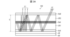
- FIG. 3A is a cross-sectional view showing a schematic configuration example of a light emitting element 102 of a comparative example.
- the light emitting element 102 of the comparative example includes a light reflective layer 30, a first electrode 31 disposed directly on the light reflective layer 30, a second electrode 35 disposed above the first electrode 31, and a first electrode 35 disposed above the first electrode 31.
- a light emitting layer 33 is provided between the electrode 31 and the second electrode 35.
- the light emitting element 102 of the comparative example has a cavity C formed between the upper surface position of the light reflective layer 30 and the lower surface position of the second electrode 35.
- the optical path length for the light L2 emitted in a direction forming an acute angle with respect to the normal to the second electrode 35 is longer than the optical path length for the light L1 emitted in parallel to the normal to the second electrode 35. long.
- FIG. 3B shows the distribution characteristics of the intensity with respect to the wavelength of the light L1 (hereinafter referred to as "wavelength-intensity characteristics") and the wavelength--of the light L2 emitted from the light emitting element 102 of the comparative example shown in FIG. 3A. strength characteristics.
- FIG. 3B shows wavelength-intensity characteristics normalized so that the brightness of the light L1 and the light L2 are equal. Specifically, the wavelength-intensity characteristics are shown when the intensity of light emitted by the light-emitting layer 33 is constant regardless of the wavelength.
- the wavelength-intensity characteristic of the light L2 is shifted to the longer wavelength side with respect to the wavelength-intensity characteristic of the light L1.
- One maximum value is seen in the wavelength-intensity characteristic of the light L1, and the wavelength corresponding to the maximum value (so-called "peak wavelength") is defined as x.
- Another maximum value is found in the wavelength-intensity characteristic of the light L2, and the peak wavelength corresponding to the maximum value is x+ ⁇ x. ⁇ x>0.
- the intensity of light emitted by the light emitting layer 33 usually differs depending on the wavelength. Therefore, the brightness of the light L1 and the light L2 in the light emitting element 102 of the comparative example is different, and the difference in brightness becomes larger as the wavelength shift amount ⁇ x is larger, that is, the brightness of the light L2 is different from the normal to the second electrode Ed2.
- the larger the angle formed by the emission direction the greater the value.
- the viewing angle characteristics of the light emitting element 102 of the comparative example were narrow.
- light reflection occurs at a plurality of positions among the upper surface position of the light reflection layer Rf, the upper surface position of the optical functional layer PF, and the intermediate position in the optical functional layer PF.
- FIG. 2 a case where light reflection occurs at the upper surface position of the light reflecting layer Rf, the upper surface position of the optical functional layer PF, and an intermediate position between the two in the optical functional layer PF will be described below.
- the light emitting element 2 is formed between (1) a cavity C1 formed between the upper surface position of the light reflecting layer Rf and the lower surface position of the second electrode Ed2; a cavity C2 formed between the lower surface position of the second electrode Ed2; and (3) cavities C3 and C4 formed between the intermediate position in the optical functional layer PF and the lower surface position of the second electrode Ed2.
- the optical path length of each of these cavities C1 to C4 is longer than the optical path length for the parallel light L1.
- FIG. 4 shows the wavelength-intensity characteristics of the light L1 that is emitted from the light emitting element 2 shown in FIG. 2 to the outside in parallel to the normal line of the second electrode Ed2.
- FIG. 5 shows the wavelength-intensity characteristics of the light L2 that is emitted from the light emitting element 2 shown in FIG. 2 to the outside in a direction forming an acute angle with respect to the normal to the second electrode Ed2. Note that FIGS. 4 and 5 also show normalized wavelength-intensity characteristics. As shown in FIG.
- the wavelength-intensity characteristics of the light L1 are a wavelength-intensity characteristic P1 due to the cavity C1, a wavelength-intensity characteristic P2 due to the cavity C2, a wavelength-intensity characteristic P3 due to the cavity C3, and a wavelength-intensity characteristic due to the cavity C4.
- the wavelength-intensity characteristics of the light L2 are a wavelength-intensity characteristic P11 due to the cavity C1, a wavelength-intensity characteristic P12 due to the cavity C2, a wavelength-intensity characteristic P13 due to the cavity C3, and a wavelength-intensity characteristic due to the cavity C4. This is a synthesis with P14.
- the peak wavelength corresponding to the maximum value of the wavelength-intensity characteristic P1 is x
- the peak wavelength corresponding to the maximum value of the wavelength-intensity characteristic P2 is x- ⁇
- the peak wavelength corresponding to the maximum value of the wavelength-intensity characteristic P3 is Let x- ⁇ be x- ⁇ , and the peak wavelength corresponding to the maximum value of the wavelength-intensity characteristic P2 be x- ⁇ . x> ⁇ > ⁇ > ⁇ >0.
- x+ ⁇ x be the peak wavelength corresponding to the maximum value of the wavelength-intensity characteristic P11
- x- ⁇ + ⁇ (x- ⁇ ) be the peak wavelength corresponding to the maximum value of the wavelength-intensity characteristic P12
- the maximum value of the wavelength-intensity characteristic P11 be Let the corresponding peak wavelength be x- ⁇ + ⁇ (x- ⁇ ), and let the peak wavelength corresponding to the maximum value of the wavelength-intensity characteristic P12 be x- ⁇ + ⁇ (x- ⁇ ).
- the viewing angle characteristics of the light emitting element 2 according to the present embodiment are wider than the light emitting element 102 of the comparative example. Note that similarly, when the light emitting element 2 according to the present embodiment has two or three cavities, and when it has five or more cavities, the light emitting element 2 according to the present embodiment is compared with the light emitting element 102 of the comparative example. The viewing angle characteristic of the light emitting element 2 is wide.
- the peak wavelength corresponding to each of the plurality of maximum values found in the wavelength-intensity characteristic of the light L2 is included in the wavelength range of one primary color.
- the wavelength range of the primary colors is, for example, a blue wavelength range of 440 nm to 490 nm, a green wavelength range of 500 nm to 570 nm, or a red wavelength range of 620 nm to 790 nm.
- the total thickness of the optical functional layer PF is preferably 10 nm to 300 nm.
- FIG. 6 is a cross-sectional view showing a schematic configuration example of the light emitting element 2 according to the present embodiment.
- the light emitting element 2 according to the present embodiment is placed on the backplane BP such that the first electrode Ed1 is located on the backplane BP side and the second electrode Ed2 is located on the display surface side. It is provided.
- the backplane BP may be provided with circuit elements and wiring for driving and controlling the light emitting elements 2.
- the light emitting element 2 has the following points, except that the optical functional layer PF includes a transparent film TF made of a transparent material and one or more pairs of semi-reflective films HR located on the corresponding transparent film TF. This is the same as the light emitting element 2 according to the first embodiment described above.
- the configuration example shown in FIG. 6 is an example in which the optical functional layer PF according to the present embodiment includes three pairs of transparent films TF and semi-reflective films HR.
- the transparent film TF located on the light reflective layer Rf will be referred to as "first transparent film TF1”
- the light semi-reflective film HR located on first transparent film TF1 will be referred to as "first semi-reflective film”.
- the transparent film TF located on the first semi-reflective film HR1 is called “second transparent film TF2”
- the optical semi-reflective film HR located on the second transparent film TF2 is called "second semi-reflective film HR2".
- the transparent film TF located on the second semi-reflective film HR2 is referred to as the "third transparent film TF3"
- the optical semi-reflective film HR located on the third transparent film TF3 is referred to as the "third semi-reflective film HR3”.
- light reflection occurs at the upper surface position of the light reflecting layer Rf, the upper surface position of the optical functional layer PF, and an intermediate position in the optical functional layer PF.
- the upper surface position of the optical functional layer PF includes the upper surface position of the third semi-reflective film HR3.
- the intermediate position in the optical functional layer PF includes the upper surface position of the first semi-reflective film HR1 and the upper surface position of the second semi-reflective film HR2.
- the semi-reflective film HR is formed thinly so that a part of the light emitted by the light-emitting layer Em1 passes through the optical functional layer PF and reaches the light-reflecting layer Rf. Therefore, the transparent film TF may be formed thicker than the corresponding semi-reflective film HR.
- the first transparent film TF1 is thicker than the first semi-reflective film HR1.
- the thickness of the semi-reflective film HR may be, for example, 1 nm or more and 10 nm or less.
- the thickness of each semi-reflective film HR may be the same or different.
- the thickness of each transparent film TF may be the same or different.
- the semi-reflective film HR includes a light reflective material.
- the semi-reflective film HR may, for example, contain reflective metals such as Ag, Al and Mg, or may contain reflective inorganic oxides such as TiO. It is preferable that the semi-reflective film HR has conductivity.
- the transparent substance constituting the transparent film TF may include an inorganic substance or an organic substance.
- transparent inorganic substances include InSnO, InGaZnO, InZnO, silicon nitride (SiN), silicon oxide (SiO), and silicon nitride oxide (SiNO).
- transparent organic materials include acrylic resins, methacrylic resins, epoxy resins, polyimide resins, and polyamide resins. It is preferable that the transparent substance constituting the transparent film TF has electrical conductivity.
- transparent conductive inorganic materials include InTiO, InGaZnO, and InZnO.
- Transparent conductive organic materials include, for example, polyphenylene, poly(p-phenylene vinylene), polythiophene, polyfluorene, and polycarbazole.
- the charge functional layer CF1 and the charge functional layer CF2 each include a hole injection layer HJ, a hole transport layer HT, a hole transporting electron blocking layer EB, an electron injection layer EJ, an electron transporting layer ET, and an electron transporting positive layer.
- One or more of the hole blocking layers HB etc. may be included as appropriate.
- FIG. 7 is a cross-sectional view showing a schematic configuration example of the light emitting element 2 according to the present embodiment.
- the optical functional layer PF includes one or more sets of a transparent film TF and a plurality of light reflectors NS disposed above the corresponding transparent film TF. Except for this point, it is the same as the light emitting element 2 according to the first and second embodiments described above.
- Each of the light reflectors NS is a particle containing a light reflective substance.
- the configuration example shown in FIG. 7 is an example in which the optical functional layer PF according to the present embodiment includes three pairs of transparent films TF and a group of light reflectors NS.
- the transparent film TF located on the light reflective layer Rf will be referred to as “first transparent film TF1”
- the light reflector NS located on first transparent film TF1 will be referred to as “first light reflector NS1”.
- the optical semi-reflective film HR located on the first light reflector NS1 is referred to as the "first semi-reflective film HR1”
- the transparent film TF located on the first semi-reflective film HR1 is referred to as the "second transparent film TF2”.
- the light reflector NS located on the second transparent film TF2 is referred to as the "second light reflector NS2"
- the transparent film TF located on the second light reflector NS2 is referred to as the "third transparent film TF3”.
- the light reflector NS located on the third transparent film TF3 is referred to as a "third light reflector NS3".
- light reflection occurs at the upper surface position of the light reflecting layer Rf, the upper surface position of the optical functional layer PF, and an intermediate position in the optical functional layer PF.
- the top surface position of the optical functional layer PF includes the top surface position of the third light reflector NS3.
- the intermediate position in the optical functional layer PF includes the upper surface position of the first light reflector NS1 and the upper surface position of the second light reflector NS2.
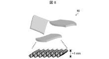
- FIG. 8 is a schematic diagram showing a schematic configuration example of the light reflector NS shown in FIG. 7.
- Each of the light reflectors NS may be a light-reflecting nanoparticle or a light-reflecting sheet.
- the light reflector NS may be a so-called "nanosheet particle" as shown in FIG. Nanosheet particles, for example, have a thickness of about 1 nm and a diameter of several tens of nanometers to several hundred nanometers.
- a 50 nm thick Ag layer was formed on the backplane BP by vapor deposition.
- an InZnO film with a thickness of 60 nm was formed on the light reflection layer Rf by sputtering.
- an alcohol solution containing a 1 nm thick sheet of titanium oxide was prepared, and the alcohol solution was applied onto the first transparent film TF1 and dried in the solvent. As a result, the sheet of titanium oxide was placed on the first transparent film TF1 as the first light reflector NS1.
- a 15 nm thick InZnO film was formed on the first light reflector NS1 by sputtering.
- the second light reflector NS2 the above-mentioned sheet body of titanium oxide was arranged in the same way as the first light reflector NS1. The process was performed again to form a third transparent film TF3, and a third light reflector NS3 was disposed.
- the first electrode Ed1 a 20 nm thick InSnO film was formed on the third light reflector NS3 by sputtering.
- the charge functional layer CF1 a hole injection layer HJ, a hole transport layer HT, and a hole transporting electron block layer EB were formed in this order.
- an organic light-emitting layer that emits blue fluorescence was formed as the light-emitting layer Em1.
- an electron injection layer EJ, an electron transport layer ET, and an electron transport hole blocking layer HB were formed in this order.
- the second electrode Ed2 a thin film of an alloy containing magnesium (Mg) and silver (Ag) was formed by sputtering. The thickness of the MgAg alloy thin film was 10 nm.
- the first electrode Ed1 was the anode
- the second electrode Ed2 was the cathode
- the film forming conditions for the InZnO film in this example are such that the oxygen doping amount is 6.3% in any of the first transparent film TF1, second transparent film TF2, and third transparent film TF3, and the film forming temperature is The temperature was 250 degrees Celsius, and the sputtering voltage was 330V.
- the front luminance ratio of the light emitting element 2 in the 50° direction was approximately 65%. Therefore, the viewing angle characteristics were wide. Further, the external quantum efficiency (EQE) was 13.8%, and the chromaticity was (0.137, 0.048) in the CIE1976 color system. Under the conditions of 25 degrees Celsius and 50 mA/cm 2 , the lifetime until the front brightness of the light emitting element 2 became 95% of the initial front brightness was 240 hours.
- the "front brightness ratio in the 50° direction” is the ratio of the 50° brightness to the front brightness
- the "front brightness” is the brightness when the light emitting element 2 is viewed from a direction parallel to the normal line of the second electrode Ed2.
- the "50° brightness” is the brightness when the light emitting element 2 is viewed from a direction that forms an acute angle of 50° with respect to the normal line of the second electrode Ed2.
- the light-emitting element 2 is arranged such that the maximum brightness angles due to the optical interference effect of the cavities C1, C2, C3, and C4 of the light emitted by the light-emitting layer Em1 are 0°, 50°, 10°, and 30°, respectively. , was designed.
- the emission peak wavelength of the light emitting layer Em1 was 456 nm, and the half width of the emission spectrum was 26 nm.
- the refractive index of the optical functional layer PF was 1.74, and the total thickness of the optical functional layer PF was 93 nm.
- the light-emitting element 102 of the comparative example was designed so that the maximum brightness angle due to the optical interference effect of the cavity C of the light emitted by the light-emitting layer Em1 was 0°.
- the "maximum brightness angle” is the angle with respect to the normal line of the second electrode Ed2 at which the intensity of light emitted from the light emitting element 2 to the outside becomes maximum.
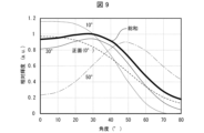
- FIG. 9 shows the angle-intensity characteristics of the light optically interfered by each of the cavities C1, C2, C3, and C4 according to this embodiment, and the angle-intensity characteristics of the light that is the sum of those lights.
- the angle-intensity characteristic due to cavity C1 is indicated by a broken line
- the angle-intensity characteristic due to cavity C2 is indicated by a dashed line
- the angle-intensity characteristic due to cavity C3 is indicated by a dotted line
- the angle-intensity characteristic due to cavity C4 is indicated by a thin solid line.
- the summed angle-intensity characteristics are shown by thick solid lines.
- the front luminance ratio in the 50° direction was about 70%. In this way, the light emitting element 2 according to this embodiment has wide viewing angle characteristics.
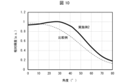
- FIG. 10 shows the angle-intensity characteristics of the light-emitting element 2 according to this example and the angle-intensity characteristics of the light-emitting element 102 of the comparative example.
- the angle-intensity characteristics according to this embodiment shown in FIG. 10 are the same as the summed angle-intensity characteristics shown in FIG.
- the light emitting element 2 according to the present example has clearly improved brightness characteristics in the oblique direction compared to the light emitting element 102 of the comparative example.
- the light reflection layer Rf was formed in the same manner as in Example 1, and then, as the first transparent film TF1, a 40 nm thick acrylic polymer resin film was formed on the light reflection layer Rf by a coating method.
- the first light reflector NS1 15 nm-thick silver nanosheet particles whose surfaces were modified with alkyl groups were placed on the first transparent film TF1.
- the second transparent film TF2 was formed in the same manner as the first transparent film TF1, and the second light reflector NS2 was arranged in the same manner as the first light reflector NS1. The process was performed again to form a third transparent film TF3, and a third light reflector NS3 was disposed.
- Example 1 the first electrode Ed1 and charge functional layer CF1 were formed in the same manner as in Example 1. Next, an organic light-emitting layer that emits green phosphorescence was formed as the light-emitting layer Em1. Next, a charge functional layer CF2 and a second electrode Ed2 were formed in the same manner as in Example 1.
- the first electrode Ed1 was the anode
- the second electrode Ed2 was the cathode.
- the front luminance ratio of the light emitting element 2 in the 50° direction was approximately 80%. Therefore, the viewing angle characteristics were wide.
- the external quantum efficiency (EQE) is 34.5%
- the chromaticity is (0.254, 0.710) in the CIE1976 color system
- the light emission is achieved under the conditions of 25 degrees Celsius and 30 mA/ cm2 .
- the lifetime until the front brightness of element 2 reached 95% of the initial front brightness was 180 hours.
- the light-emitting element 2 is arranged such that the maximum brightness angles due to the optical interference effect of the cavities C1, C2, C3, and C4 of the light emitted by the light-emitting layer Em1 are 0°, 50°, 20°, and 40°, respectively. , was designed.
- the emission peak wavelength of the light emitting layer Em1 was 532 nm, and the half width of the emission spectrum was 56 nm.
- the refractive index of the optical functional layer PF was 1.74, and the total thickness of the optical functional layer PF was approximately 185 nm.
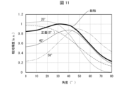
- FIG. 11 shows the angle-intensity characteristics of the light optically interfered by each of the cavities C1, C2, C3, and C4 according to this embodiment, and the angle-intensity characteristics of the light that is the sum of those lights.
- the angle-intensity characteristic due to cavity C1 is indicated by a broken line
- the angle-intensity characteristic due to cavity C2 is indicated by a dashed line
- the angle-intensity characteristic due to cavity C3 is indicated by a dotted line
- the angle-intensity characteristic due to cavity C4 is indicated by a thin solid line.
- the summed angle-intensity characteristics are shown by thick solid lines.
- the front luminance ratio in the 50° direction was about 80%. In this way, the light emitting element 2 according to this embodiment has wide viewing angle characteristics.
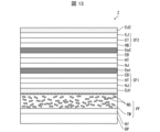
- FIG. 12 is a cross-sectional view showing a schematic configuration example of the light emitting element 2 according to the present embodiment.
- the light emitting element 2 according to the present embodiment has the following exceptions: the optical functional layer PF includes a transparent medium TM made of a transparent material and a plurality of light reflectors NS disposed in the transparent medium TM. , is the same as the light emitting device 2 according to the first to third embodiments described above.
- the light reflectors NS may be randomly scattered in the transparent medium TM or may be aligned.
- light reflection occurs at the upper surface position of the light reflection layer Rf and at an intermediate position in the optical functional layer PF.
- the intermediate position in the optical functional layer PF includes the upper surface position of the light reflector NS.
- the transparent substance constituting the transparent medium TM may contain an inorganic substance or an organic substance, similarly to the transparent substance constituting the transparent film TF. Moreover, it is preferable to have conductivity.
- the light reflector NS is a sheet body, the light reflector NS may be oriented so that the widest surface of the light reflector NS generally faces the normal direction of the second electrode Ed2 (vertical direction in FIG. 12). .
- the mass ratio of the light reflector NS to the transparent medium TM may be 10% to 95%.
- a light reflection layer Rf was formed in the same manner as in Example 1, and then, as an optical functional layer PF, a mixture of InSnO and titanium oxide nanosheets was formed on the light reflection layer Rf by sputtering.
- the total thickness of the optical functional layer PF was 18 nm
- InSnO constituted the transparent medium TM
- titanium oxide nanosheet constituted the light reflector NS.
- the thickness of the titanium oxide nanosheets was 1 nm, and the diameter ranged from several tens of nm to several ⁇ m. Due to its shape, the titanium oxide nanosheets were oriented so that the widest surface faced the normal direction of the second electrode Ed2.
- Example 1 the first electrode Ed1 and charge functional layer CF1 were formed in the same manner as in Example 1. Next, an organic light-emitting layer that emits blue fluorescence was formed as the light-emitting layer Em1. Next, a charge functional layer CF2 and a second electrode Ed2 were formed in the same manner as in Example 1.
- the first electrode Ed1 was the anode
- the second electrode Ed2 was the cathode.
- the conditions for forming the InSnO film in this example were that the oxygen doping amount was 17.3%, the film forming temperature was 250 degrees Celsius, and the sputtering voltage was 250V.
- the front luminance ratio of the light emitting element 2 in the 50° direction was approximately 62%. Therefore, the viewing angle characteristics were wide.
- the external quantum efficiency (EQE) is 12.2%
- the chromaticity is (0.136, 0.047) in the CIE1976 color system
- the light emission is achieved under the conditions of 25 degrees Celsius and 50 mA/ cm2 .
- the lifetime until the front brightness of element 2 reached 95% of the initial front brightness was 265 hours.
- FIG. 13 is a cross-sectional view showing a schematic configuration example of the light emitting element 2 according to the present embodiment.
- the light emitting element 2 according to the present embodiment has a light emitting layer between the first electrode Ed1 and the second electrode Ed2.
- Another light-emitting layer Em2 that emits light of the same color as Em1 is arranged.
- the light emitting layer Em2 may be an organic light emitting layer containing an organic material that emits fluorescence or phosphorescence, or a quantum dot light emitting layer containing quantum dots that emit fluorescence or phosphorescence.
- the light emitting element 2 may further include a charge functional layer CF3 between the two light emitting layers Em1 and Em2.
- the charge functional layer CF3 may appropriately contain any one or more of a hole blocking layer HB, an electron transporting layer ET, a charge generation layer CG, a hole transporting layer HT, and an electron blocking layer EB having hole transporting properties. .
- a light reflecting layer Rf was formed in the same manner as in Example 1.
- the optical functional layer PF was formed in the same manner as in Example 1 except that the total thickness of the optical functional layer PF was 36 nm.
- the first electrode Ed1 and charge functional layer CF1 were formed in the same manner as in Example 1.
- an organic light-emitting layer that emits red phosphorescence was formed as the light-emitting layer Em1.
- an electron transporting hole blocking layer HB, an electron transporting layer ET, a charge generation layer CG, a hole transporting layer HT, and a hole transporting electron blocking layer EB were formed in this order.
- an organic light-emitting layer that emits red phosphorescence was formed as the light-emitting layer Em2.
- a charge functional layer CF2 and a second electrode Ed2 were formed in the same manner as in Example 1.
- the first electrode Ed1 was the anode
- the second electrode Ed2 was the cathode.
- the front luminance ratio of the light emitting element 2 in the 50° direction was approximately 80%. Therefore, the viewing angle characteristics were wide.
- the external quantum efficiency (EQE) is 65.7%
- the chromaticity is (0.692, 0.307) in the CIE1976 color system
- the light emission is achieved under the conditions of 25 degrees Celsius and 50 mA/ cm2 .
- the lifetime until the front brightness of element 2 reached 95% of the initial front brightness was 1740 hours.
- the light-emitting element 2 is arranged such that the luminance maximum angles due to the optical interference effects of the cavities C1, C2, C3, and C4 of the light emitted by the light-emitting layers Em1 and Em2 are 0°, 50°, 10°, and 40°, respectively. It was designed to be.
- the emission peak wavelength of the light emitting layers Em1 and Em2 was set to 626 nm, and the half width of the emission spectrum was set to 59 nm.
- the refractive index of the optical functional layer PF was set to 1.74, and the total thickness of the optical functional layer PF was set to about 36 nm.
- FIG. 14 shows the angle-intensity characteristics of the light optically interfered by each of the cavities C1, C2, C3, and C4 according to this embodiment, and the angle-intensity characteristics of the light that is the sum of those lights.
- the angle-intensity characteristic due to cavity C1 is indicated by a broken line
- the angle-intensity characteristic due to cavity C2 is indicated by a dashed line
- the angle-intensity characteristic due to cavity C3 is indicated by a dotted line
- the angle-intensity characteristic due to cavity C4 is indicated by a thin solid line.
- the summed angle-intensity characteristics are shown by thick solid lines.
- the front luminance ratio in the 50° direction was about 80%. In this way, the light emitting element 2 according to this embodiment has wide viewing angle characteristics.
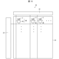
- FIG. 15 is a plan view showing a schematic configuration example of a display device according to this embodiment.
- the display device 20 includes a display section 25 including a plurality of sub-pixels SB, SG, and SR, and a driver 22 that drives the plurality of sub-pixels SB, SG, and SR.
- the sub-pixel SB includes a light emitting element ED and a pixel circuit PC connected to the light emitting element ED.
- the sub-pixel SB may be a blue sub-pixel including the light-emitting element 2 that emits blue light.
- the sub-pixel SG may be a green sub-pixel including the light-emitting element 2 that emits green light
- the sub-pixel SR may be a red sub-pixel including the light-emitting element 2 that emits red light.
- the viewing angle characteristics of the light emitting element 102 of the comparative example are narrow.
- the viewing angle characteristics of blue light emitting devices, green light emitting devices and red light emitting devices are usually different.
- a display device including the light-emitting elements 102 of the comparative example as a blue light-emitting element, a green light-emitting element, and a red light-emitting element there was a problem that when a white display screen was viewed from an oblique direction, the screen appeared colored. Furthermore, there is also the problem that the brightness of the display screen of the display device 4 is lower when viewed from an angle than when viewed from the front.
- the light emitting element 2 according to the present disclosure has wide viewing angle characteristics. Therefore, in a display device including the light-emitting element 2 according to the present disclosure as a blue light-emitting element, a green light-emitting element, and a red light-emitting element, even when a screen displaying white is viewed from an oblique direction, the screen is hardly colored.
- the front luminance ratio in the 50° direction is about 60% or more or about 80% or more
- the brightness ratio is 50% or more compared to when viewed from the front. Even when the display screen is viewed from a direction that forms an acute angle of °, the screen does not become very colored or dark.
Landscapes
- Physics & Mathematics (AREA)
- Optics & Photonics (AREA)
- Electroluminescent Light Sources (AREA)
Abstract
Description
(発光素子の断面構成)
図1は、本実施形態に係る発光素子2の構成例を示す断面図である。図1に示すように、発光素子2は、光反射層Rfと、光反射層Rfの上方に配された第1電極Ed1と、第1電極Ed1の上方に配された第2電極Ed2と、第1電極Ed1および第2電極Ed2の間に配された発光層Em1と、光反射層Rfおよび第1電極Ed1の間に配され、光反射率が光反射層Rfよりも小さく第1電極Ed1よりも大きい光学機能層PFとを備えている。
図3Aは、比較例の発光素子102の概略構成例を示す断面図である。比較例の発光素子102は、光反射層30と、光反射層30の上に直に配された第1電極31と、第1電極31の上方に配された第2電極35と、第1電極31および第2電極35の間に配された発光層33とを備える。
本開示の他の実施形態について、以下に説明する。なお、説明の便宜上、上記実施形態にて説明した部材と同じ機能を有する部材については、同じ符号を付記し、その説明を繰り返さない。
本開示の他の実施形態について、以下に説明する。なお、説明の便宜上、上記実施形態にて説明した部材と同じ機能を有する部材については、同じ符号を付記し、その説明を繰り返さない。
本開示の他の実施形態について、以下に説明する。なお、説明の便宜上、上記実施形態にて説明した部材と同じ機能を有する部材については、同じ符号を付記し、その説明を繰り返さない。
本開示の他の実施形態について、以下に説明する。なお、説明の便宜上、上記実施形態にて説明した部材と同じ機能を有する部材については、同じ符号を付記し、その説明を繰り返さない。
本開示の他の実施形態について、以下に説明する。なお、説明の便宜上、上記実施形態にて説明した部材と同じ機能を有する部材については、同じ符号を付記し、その説明を繰り返さない。
20 表示装置
Rf 光反射層
Ed1 第1電極
Ed2 第2電極
PF 光学機能層
TF 透明膜
TF1 第1透明膜
TF2 第2透明膜
HR 半反射膜
HR1 第1半反射膜
HR2 第2半反射膜
NS 光反射体
TM 透明媒体
Claims (23)
- 光反射層と、
前記光反射層の上方に配された第1電極と、
前記第1電極の上方に配された第2電極と、
前記第1電極および第2電極間に配された発光層と、
前記光反射層および前記第1電極の間に配され、光反射率が前記光反射層よりも小さく前記第1電極よりも大きい光学機能層と、を備える発光素子。 - 前記光学機能層の上面位置、前記光反射層の上面位置、前記光学機能層中の中間位置のうちの複数の位置で光反射が生じる、請求項1に記載の発光素子。
- 前記第2電極から、前記第2電極の法線に対して鋭角をなす方向に出射する光の波長-強度特性に複数の極大値が見られ、
前記複数の極大値それぞれに対応する波長が1つの原色の波長域に含まれる、請求項2に記載の発光素子。 - 前記光学機能層の厚さは、10nm~300nmである、請求項1~3のいずれか1項に記載の発光素子。
- 前記光学機能層は、前記光反射層上に位置し、透明物質からなる第1透明膜を含む、請求項1~4のいずれか1項に記載の発光素子。
- 前記光学機能層は、前記第1透明膜上に位置する第1半反射膜を含む、請求項5に記載の発光素子。
- 前記光学機能層は、前記第1半反射膜上に位置する第2透明膜と、前記第2透明膜上に位置する第2半反射膜とを含む、請求項6に記載の発光素子。
- 前記第1透明膜は前記第1半反射膜よりも厚い、請求項6に記載の発光素子。
- 前記第1半反射膜の厚さは、1nm以上10nm未満である、請求項6~8のいずれか1項に記載の発光素子。
- 前記第1半反射膜は、Ag、Al、TiおよびMgの少なくとも1つを含む、請求項6~9のいずれか1項に記載の発光素子。
- 前記光学機能層は、前記第1透明膜の上方に配された複数の光反射体を含む、請求項5に記載の発光素子。
- 前記光学機能層は、透明物質からなる透明媒体と、前記透明媒体中に配された複数の光反射体とを含む、請求項1~4のいずれか1項に記載の発光素子。
- 前記透明媒体に対する前記複数の光反射体の質量割合が10~95%である、請求項12に記載の発光素子。
- 前記複数の光反射体それぞれが光反射性のナノ粒子である、請求項11~13のいずれか1項に記載の発光素子。
- 前記複数の光反射体それぞれが光反射性のシート体である、請求項11~13のいずれか1項に記載の発光素子。
- 前記透明物質は、無機物質である、請求項5~15のいずれか1項に記載の発光素子。
- 前記無機物質は、インジウムスズ酸化物、インジウム亜鉛酸化物、インジウムガリウム亜鉛酸化物、窒化シリコン、酸化シリコン、酸窒化シリコンの少なくとも1つを含む、請求項16に記載の発光素子。
- 前記透明物質は、有機物質である、請求項5~15のいずれか1項に記載の発光素子。
- 前記有機物質は、アクリル樹脂、メタクリル樹脂、エポキシ樹脂、ポリイミド樹脂、ポリアミド樹脂の少なくとも1つを含む、請求項18に記載の発光素子。
- 前記有機物質は、導電性を有する、請求項18に記載の発光素子。
- 前記有機物質は、ポリフェニレン、ポリ(p-フェニレンビニレン)、ポリチオフェン、ポリフルオレン、およびポリカルバゾールの少なくとも1つを含む、請求項20に記載の発光素子。
- 前記第1電極および第2電極間に、前記発光層と同色発光する別の発光層が配されている、請求項1~21のいずれか1項に記載の発光素子。
- 請求項1~22のいずれか1項に記載の発光素子を含む表示装置。
Priority Applications (2)
| Application Number | Priority Date | Filing Date | Title |
|---|---|---|---|
| US18/863,408 US20250311543A1 (en) | 2022-05-10 | 2022-05-10 | Light-emitting element and display device |
| PCT/JP2022/019801 WO2023218524A1 (ja) | 2022-05-10 | 2022-05-10 | 発光素子および表示装置 |
Applications Claiming Priority (1)
| Application Number | Priority Date | Filing Date | Title |
|---|---|---|---|
| PCT/JP2022/019801 WO2023218524A1 (ja) | 2022-05-10 | 2022-05-10 | 発光素子および表示装置 |
Publications (1)
| Publication Number | Publication Date |
|---|---|
| WO2023218524A1 true WO2023218524A1 (ja) | 2023-11-16 |
Family
ID=88729991
Family Applications (1)
| Application Number | Title | Priority Date | Filing Date |
|---|---|---|---|
| PCT/JP2022/019801 Ceased WO2023218524A1 (ja) | 2022-05-10 | 2022-05-10 | 発光素子および表示装置 |
Country Status (2)
| Country | Link |
|---|---|
| US (1) | US20250311543A1 (ja) |
| WO (1) | WO2023218524A1 (ja) |
Cited By (1)
| Publication number | Priority date | Publication date | Assignee | Title |
|---|---|---|---|---|
| WO2026070481A1 (ja) * | 2024-09-30 | 2026-04-02 | ソニーグループ株式会社 | 表示装置 |
Citations (5)
| Publication number | Priority date | Publication date | Assignee | Title |
|---|---|---|---|---|
| JP2008538155A (ja) * | 2005-02-24 | 2008-10-09 | イーストマン コダック カンパニー | 光出力が改善されたoledデバイス |
| WO2013042745A1 (ja) * | 2011-09-21 | 2013-03-28 | パナソニック株式会社 | 有機エレクトロルミネッセンス素子 |
| JP2013235233A (ja) * | 2012-05-09 | 2013-11-21 | Samsung Display Co Ltd | 光学シートの製造方法、有機発光表示装置及び有機発光表示装置の製造方法 |
| KR20170115655A (ko) * | 2016-04-07 | 2017-10-18 | 한국전자통신연구원 | 이중모드 디스플레이 |
| US20210217825A1 (en) * | 2018-12-05 | 2021-07-15 | Boe Technology Group Co., Ltd. | Light emitting diode and fabrication method thereof, display substrate and display panel |
-
2022
- 2022-05-10 WO PCT/JP2022/019801 patent/WO2023218524A1/ja not_active Ceased
- 2022-05-10 US US18/863,408 patent/US20250311543A1/en active Pending
Patent Citations (5)
| Publication number | Priority date | Publication date | Assignee | Title |
|---|---|---|---|---|
| JP2008538155A (ja) * | 2005-02-24 | 2008-10-09 | イーストマン コダック カンパニー | 光出力が改善されたoledデバイス |
| WO2013042745A1 (ja) * | 2011-09-21 | 2013-03-28 | パナソニック株式会社 | 有機エレクトロルミネッセンス素子 |
| JP2013235233A (ja) * | 2012-05-09 | 2013-11-21 | Samsung Display Co Ltd | 光学シートの製造方法、有機発光表示装置及び有機発光表示装置の製造方法 |
| KR20170115655A (ko) * | 2016-04-07 | 2017-10-18 | 한국전자통신연구원 | 이중모드 디스플레이 |
| US20210217825A1 (en) * | 2018-12-05 | 2021-07-15 | Boe Technology Group Co., Ltd. | Light emitting diode and fabrication method thereof, display substrate and display panel |
Cited By (1)
| Publication number | Priority date | Publication date | Assignee | Title |
|---|---|---|---|---|
| WO2026070481A1 (ja) * | 2024-09-30 | 2026-04-02 | ソニーグループ株式会社 | 表示装置 |
Also Published As
| Publication number | Publication date |
|---|---|
| US20250311543A1 (en) | 2025-10-02 |
Similar Documents
| Publication | Publication Date | Title |
|---|---|---|
| JP4951130B2 (ja) | 有機発光素子及びその製造方法 | |
| KR101434361B1 (ko) | 백색 유기 전계 발광소자 및 이를 이용한 컬러 디스플레이장치 | |
| TWI448195B (zh) | 有機電致發光裝置,包括該有機電致發光裝置之顯示裝置及製造有機電致發光裝置之方法 | |
| JP5407910B2 (ja) | 発光装置、照明装置および表示装置 | |
| US20190189701A1 (en) | Electroluminescent display device | |
| KR101528242B1 (ko) | 백색 유기 전계 발광소자 및 이를 이용한 컬러 디스플레이장치 | |
| CN108448007B (zh) | 有机发光显示面板及其显示装置 | |
| JP2008108439A (ja) | 電界発光素子および電界発光パネル | |
| US20100327304A1 (en) | Organic el device and design method thereof | |
| US8487335B2 (en) | Light emitting device, illumination apparatus and display apparatus | |
| US11322707B2 (en) | Cadmium-free quantum dot LED with improved emission color | |
| CN110323344A (zh) | 包括具有低角度色偏移的光学腔的发光装置 | |
| KR102607857B1 (ko) | 코어쉘 구조의 나노 입자를 포함하는 발광 소자 | |
| JP2008226718A (ja) | 有機el素子 | |
| CN110199402B (zh) | 发光二极管及其制造方法、显示基板、显示设备 | |
| JP4769068B2 (ja) | 有機発光素子及びその製造方法 | |
| CN1666354B (zh) | 具有透明阴极的场致发光设备 | |
| WO2023218524A1 (ja) | 発光素子および表示装置 | |
| US10923633B2 (en) | Top-emitting light-emitting diode | |
| KR102103516B1 (ko) | 광 추출 구조체 및 유기 발광 조명 장치 | |
| US7545096B2 (en) | Trans-reflective organic electroluminescent panel and method of fabricating the same | |
| CN111162108A (zh) | 一种显示面板、其制作方法及显示装置 | |
| WO2024174678A1 (zh) | 一种显示器和显示设备 | |
| JP4990587B2 (ja) | 発光素子及びその製造方法 | |
| KR100978012B1 (ko) | 투명 캐쏘드를 구비한 전기발광 디바이스 |
Legal Events
| Date | Code | Title | Description |
|---|---|---|---|
| 121 | Ep: the epo has been informed by wipo that ep was designated in this application |
Ref document number: 22941606 Country of ref document: EP Kind code of ref document: A1 |
|
| WWE | Wipo information: entry into national phase |
Ref document number: 18863408 Country of ref document: US |
|
| NENP | Non-entry into the national phase |
Ref country code: DE |
|
| 122 | Ep: pct application non-entry in european phase |
Ref document number: 22941606 Country of ref document: EP Kind code of ref document: A1 |
|
| NENP | Non-entry into the national phase |
Ref country code: JP |
|
| WWP | Wipo information: published in national office |
Ref document number: 18863408 Country of ref document: US |