WO2023210430A1 - 表示装置 - Google Patents
表示装置 Download PDFInfo
- Publication number
- WO2023210430A1 WO2023210430A1 PCT/JP2023/015362 JP2023015362W WO2023210430A1 WO 2023210430 A1 WO2023210430 A1 WO 2023210430A1 JP 2023015362 W JP2023015362 W JP 2023015362W WO 2023210430 A1 WO2023210430 A1 WO 2023210430A1
- Authority
- WO
- WIPO (PCT)
- Prior art keywords
- switching element
- voltage
- circuit
- display device
- capacitor
- Prior art date
- Legal status (The legal status is an assumption and is not a legal conclusion. Google has not performed a legal analysis and makes no representation as to the accuracy of the status listed.)
- Ceased
Links
Images




Classifications
-
- G—PHYSICS
- G02—OPTICS
- G02F—OPTICAL DEVICES OR ARRANGEMENTS FOR THE CONTROL OF LIGHT BY MODIFICATION OF THE OPTICAL PROPERTIES OF THE MEDIA OF THE ELEMENTS INVOLVED THEREIN; NON-LINEAR OPTICS; FREQUENCY-CHANGING OF LIGHT; OPTICAL LOGIC ELEMENTS; OPTICAL ANALOGUE/DIGITAL CONVERTERS
- G02F1/00—Devices or arrangements for the control of the intensity, colour, phase, polarisation or direction of light arriving from an independent light source, e.g. switching, gating or modulating; Non-linear optics
- G02F1/01—Devices or arrangements for the control of the intensity, colour, phase, polarisation or direction of light arriving from an independent light source, e.g. switching, gating or modulating; Non-linear optics for the control of the intensity, phase, polarisation or colour
- G02F1/13—Devices or arrangements for the control of the intensity, colour, phase, polarisation or direction of light arriving from an independent light source, e.g. switching, gating or modulating; Non-linear optics for the control of the intensity, phase, polarisation or colour based on liquid crystals, e.g. single liquid crystal display cells
- G02F1/133—Constructional arrangements; Operation of liquid crystal cells; Circuit arrangements
- G02F1/136—Liquid crystal cells structurally associated with a semi-conducting layer or substrate, e.g. cells forming part of an integrated circuit
- G02F1/1362—Active matrix addressed cells
- G02F1/1368—Active matrix addressed cells in which the switching element is a three-electrode device
-
- G—PHYSICS
- G02—OPTICS
- G02F—OPTICAL DEVICES OR ARRANGEMENTS FOR THE CONTROL OF LIGHT BY MODIFICATION OF THE OPTICAL PROPERTIES OF THE MEDIA OF THE ELEMENTS INVOLVED THEREIN; NON-LINEAR OPTICS; FREQUENCY-CHANGING OF LIGHT; OPTICAL LOGIC ELEMENTS; OPTICAL ANALOGUE/DIGITAL CONVERTERS
- G02F1/00—Devices or arrangements for the control of the intensity, colour, phase, polarisation or direction of light arriving from an independent light source, e.g. switching, gating or modulating; Non-linear optics
- G02F1/01—Devices or arrangements for the control of the intensity, colour, phase, polarisation or direction of light arriving from an independent light source, e.g. switching, gating or modulating; Non-linear optics for the control of the intensity, phase, polarisation or colour
- G02F1/13—Devices or arrangements for the control of the intensity, colour, phase, polarisation or direction of light arriving from an independent light source, e.g. switching, gating or modulating; Non-linear optics for the control of the intensity, phase, polarisation or colour based on liquid crystals, e.g. single liquid crystal display cells
- G02F1/133—Constructional arrangements; Operation of liquid crystal cells; Circuit arrangements
-
- G—PHYSICS
- G02—OPTICS
- G02F—OPTICAL DEVICES OR ARRANGEMENTS FOR THE CONTROL OF LIGHT BY MODIFICATION OF THE OPTICAL PROPERTIES OF THE MEDIA OF THE ELEMENTS INVOLVED THEREIN; NON-LINEAR OPTICS; FREQUENCY-CHANGING OF LIGHT; OPTICAL LOGIC ELEMENTS; OPTICAL ANALOGUE/DIGITAL CONVERTERS
- G02F1/00—Devices or arrangements for the control of the intensity, colour, phase, polarisation or direction of light arriving from an independent light source, e.g. switching, gating or modulating; Non-linear optics
- G02F1/01—Devices or arrangements for the control of the intensity, colour, phase, polarisation or direction of light arriving from an independent light source, e.g. switching, gating or modulating; Non-linear optics for the control of the intensity, phase, polarisation or colour
- G02F1/13—Devices or arrangements for the control of the intensity, colour, phase, polarisation or direction of light arriving from an independent light source, e.g. switching, gating or modulating; Non-linear optics for the control of the intensity, phase, polarisation or colour based on liquid crystals, e.g. single liquid crystal display cells
- G02F1/133—Constructional arrangements; Operation of liquid crystal cells; Circuit arrangements
- G02F1/13306—Circuit arrangements or driving methods for the control of single liquid crystal cells
-
- G—PHYSICS
- G02—OPTICS
- G02F—OPTICAL DEVICES OR ARRANGEMENTS FOR THE CONTROL OF LIGHT BY MODIFICATION OF THE OPTICAL PROPERTIES OF THE MEDIA OF THE ELEMENTS INVOLVED THEREIN; NON-LINEAR OPTICS; FREQUENCY-CHANGING OF LIGHT; OPTICAL LOGIC ELEMENTS; OPTICAL ANALOGUE/DIGITAL CONVERTERS
- G02F1/00—Devices or arrangements for the control of the intensity, colour, phase, polarisation or direction of light arriving from an independent light source, e.g. switching, gating or modulating; Non-linear optics
- G02F1/01—Devices or arrangements for the control of the intensity, colour, phase, polarisation or direction of light arriving from an independent light source, e.g. switching, gating or modulating; Non-linear optics for the control of the intensity, phase, polarisation or colour
- G02F1/13—Devices or arrangements for the control of the intensity, colour, phase, polarisation or direction of light arriving from an independent light source, e.g. switching, gating or modulating; Non-linear optics for the control of the intensity, phase, polarisation or colour based on liquid crystals, e.g. single liquid crystal display cells
- G02F1/133—Constructional arrangements; Operation of liquid crystal cells; Circuit arrangements
- G02F1/136—Liquid crystal cells structurally associated with a semi-conducting layer or substrate, e.g. cells forming part of an integrated circuit
- G02F1/1362—Active matrix addressed cells
- G02F1/136213—Storage capacitors associated with the pixel electrode
-
- G—PHYSICS
- G09—EDUCATION; CRYPTOGRAPHY; DISPLAY; ADVERTISING; SEALS
- G09F—DISPLAYING; ADVERTISING; SIGNS; LABELS OR NAME-PLATES; SEALS
- G09F9/00—Indicating arrangements for variable information in which the information is built-up on a support by selection or combination of individual elements
- G09F9/30—Indicating arrangements for variable information in which the information is built-up on a support by selection or combination of individual elements in which the desired character or characters are formed by combining individual elements
-
- G—PHYSICS
- G09—EDUCATION; CRYPTOGRAPHY; DISPLAY; ADVERTISING; SEALS
- G09G—ARRANGEMENTS OR CIRCUITS FOR CONTROL OF INDICATING DEVICES USING STATIC MEANS TO PRESENT VARIABLE INFORMATION
- G09G3/00—Control arrangements or circuits, of interest only in connection with visual indicators other than cathode-ray tubes
- G09G3/20—Control arrangements or circuits, of interest only in connection with visual indicators other than cathode-ray tubes for presentation of an assembly of a number of characters, e.g. a page, by composing the assembly by combination of individual elements arranged in a matrix no fixed position being assigned to or needed to be assigned to the individual characters or partial characters
-
- G—PHYSICS
- G09—EDUCATION; CRYPTOGRAPHY; DISPLAY; ADVERTISING; SEALS
- G09G—ARRANGEMENTS OR CIRCUITS FOR CONTROL OF INDICATING DEVICES USING STATIC MEANS TO PRESENT VARIABLE INFORMATION
- G09G3/00—Control arrangements or circuits, of interest only in connection with visual indicators other than cathode-ray tubes
- G09G3/20—Control arrangements or circuits, of interest only in connection with visual indicators other than cathode-ray tubes for presentation of an assembly of a number of characters, e.g. a page, by composing the assembly by combination of individual elements arranged in a matrix no fixed position being assigned to or needed to be assigned to the individual characters or partial characters
- G09G3/34—Control arrangements or circuits, of interest only in connection with visual indicators other than cathode-ray tubes for presentation of an assembly of a number of characters, e.g. a page, by composing the assembly by combination of individual elements arranged in a matrix no fixed position being assigned to or needed to be assigned to the individual characters or partial characters by control of light from an independent source
- G09G3/36—Control arrangements or circuits, of interest only in connection with visual indicators other than cathode-ray tubes for presentation of an assembly of a number of characters, e.g. a page, by composing the assembly by combination of individual elements arranged in a matrix no fixed position being assigned to or needed to be assigned to the individual characters or partial characters by control of light from an independent source using liquid crystals
-
- G—PHYSICS
- G03—PHOTOGRAPHY; CINEMATOGRAPHY; ANALOGOUS TECHNIQUES USING WAVES OTHER THAN OPTICAL WAVES; ELECTROGRAPHY; HOLOGRAPHY
- G03B—APPARATUS OR ARRANGEMENTS FOR TAKING PHOTOGRAPHS OR FOR PROJECTING OR VIEWING THEM; APPARATUS OR ARRANGEMENTS EMPLOYING ANALOGOUS TECHNIQUES USING WAVES OTHER THAN OPTICAL WAVES; ACCESSORIES THEREFOR
- G03B21/00—Projectors or projection-type viewers; Accessories therefor
- G03B21/005—Projectors using an electronic spatial light modulator but not peculiar thereto
- G03B21/006—Projectors using an electronic spatial light modulator but not peculiar thereto using LCD's
Definitions
- the present disclosure relates to a display device.
- Patent Document 1 A pulse width modulation (PWM) type display device that controls a light emission period according to the gradation of each pixel is known (see Patent Document 1).
- PWM pulse width modulation
- the size of the pixel circuit is reduced by omitting a buffer between a liquid crystal element and a selection circuit that selects data in a memory provided in the pixel circuit.
- Logic circuits that perform logical operations on digital signals operate with low power consumption of about 1V, whereas it is necessary to apply a voltage of 3V or more to liquid crystal elements. For this reason, pixel circuits are often configured with circuits whose voltage level corresponds to the drive voltage of the liquid crystal element. More specifically, the transistors in the pixel circuit are configured with medium or high voltage transistors. Medium or high voltage transistors are larger in size and consume more power than low voltage transistors used in logic circuits.
- pulse width modulation type display devices require memory with an SRAM (Static Random Access Memory) configuration in the pixel circuit, which increases the circuit area of the pixel circuit and increases power consumption. do.
- SRAM Static Random Access Memory
- Pulse width modulation type display devices have the potential to be applied to various digital devices, so further miniaturization, lower power consumption, and higher image quality are desired.
- the present disclosure provides a display device that can be made smaller, consume less power, and have higher image quality.
- the pixel includes a display element and a pixel circuit that controls a voltage supplied to the display element,
- the pixel circuit is a capacitor that holds charge according to the voltage supplied to the display element; a charging/discharging circuit that charges and discharges the capacitor; a control circuit that controls the charging and discharging circuit;
- the charging/discharging circuit is a first switching element that controls charging of the capacitor; a second switching element that controls discharge of the capacitor;
- a display device is provided, wherein the control circuit includes a third switching element that controls on or off of at least one of the first switching element and the second switching element based on at least one of pixel data or a display timing signal. be done.
- the first switching element and the second switching element may have the same breakdown voltage and the same conductivity type.
- the first switching element and the second switching element in the charging/discharging circuit have a first breakdown voltage
- the third switching element in the control circuit may have a second breakdown voltage lower than the first breakdown voltage
- the first switching element, the second switching element, and the third switching element are cascode-connected between a first reference voltage node and a second reference voltage node,
- the capacitor may be connected between a connection node between the first switching element and the second switching element and the second reference voltage node.
- the third switching element may have the same breakdown voltage and the same conductivity type as the first switching element and the second switching element.
- the third switching element may have a different breakdown voltage and the same conductivity type as the first switching element and the second switching element.
- the first switching element and the second switching element are connected in cascode between a first reference voltage node and a second reference voltage node,
- the capacitor may be connected between a connection node between the first switching element and the second switching element and the second reference voltage node.
- the control circuit may generate a control signal to be input to a gate of at least one of the first switching element and the second switching element, based on the pixel data and the display timing signal.
- a precharge signal may be input to the gate of either the first switching element or the second switching element, and the control signal may be input to the other gate.
- the voltage amplitude of the precharge signal may be larger than the voltage amplitude of the control signal.
- the voltage amplitude of the precharge signal may be larger than the voltage amplitudes of the pixel data and the display timing signal.
- a first drive circuit may be provided that sets the voltage level of the precharge signal in consideration of the threshold voltage of the first switching element or the second switching element.
- the first switching element and the second switching element are N-type MOS (Metal Oxide Semiconductor) transistors,
- the drain of the first switching element is connected to a first reference voltage node, one end of the capacitor is connected to the source of the first switching element,
- the first drive circuit adjusts the voltage level of the precharge signal to the first reference voltage node so that the source of the first switching element has the same voltage level as the first reference voltage node when charging the capacitor.
- the voltage may be set higher than the voltage by the threshold voltage.
- the first switching element and the second switching element are P-type MOS (Metal Oxide Semiconductor) transistors,
- the source of the first switching element is connected to a first reference voltage node
- the drain of the second switching element is connected to a second reference voltage node
- one end of the capacitor is connected to the drain of the first switching element
- the first drive circuit adjusts the voltage level of the precharge signal to the second reference voltage node so that the drain of the first switching element becomes the same voltage level as the second reference voltage node when the capacitor is discharged.
- the voltage may be set to be lower than the voltage by the threshold voltage.
- the first drive circuit sends the precharge signal having a voltage amplitude larger than the voltage amplitude of the control circuit and the display timing signal having a voltage amplitude comparable to the voltage amplitude of the control circuit to the control circuit. You can also enter it.
- the charging/discharging circuit is a diode or a diode-connected transistor connected to the gate of the first switching element;
- the device may further include a compensation circuit that compensates for a decrease in the charging voltage of the capacitor caused by inputting the precharge signal to the gate of the first switching element via the diode or the diode-connected transistor. .
- the first reference voltage of the first reference voltage node and the second reference voltage of the second reference voltage node are voltages with opposite voltage polarities,
- the precharge signal supplied to the gate of the first switching element and the display timing signal may have opposite voltage polarities.
- the precharge signal supplied to the gate of the first switching element and the pixel data have opposite voltage polarities
- the control circuit may be supplied with the first reference voltage or the second reference voltage, and an intermediate voltage between the first reference voltage and the second reference voltage.
- the first switching element and the second switching element may have the same breakdown voltage and different conductivity types.
- FIG. 1 is a diagram illustrating an example of the overall configuration of a display system including a display device according to an embodiment.
- FIG. 2 is a block diagram showing a schematic configuration of the liquid crystal light valve shown in FIG. 1.
- FIG. 3 is a circuit diagram of a pixel circuit according to a comparative example.
- FIG. 3 is a circuit diagram of a pixel circuit according to a first specific example.
- FIG. 3 is a circuit diagram of a pixel circuit according to a second specific example.
- FIG. 7 is a circuit diagram of a pixel circuit according to a third specific example.
- FIG. 7 is a circuit diagram of a pixel circuit according to a fourth specific example.
- FIG. 7 is a circuit diagram of a pixel circuit according to a fifth specific example.
- FIG. 7 is a circuit diagram of a pixel circuit according to a sixth specific example.
- FIG. 3 is a diagram showing the inside of the vehicle from the rear to the front of the vehicle. A diagram showing the interior of the vehicle from diagonally rearward to diagonally forward.
- FIG. 7 is a front view of a digital camera that is a second application example of the electronic device. Rear view of the digital camera.
- FIG. 3 is an external view of an HMD, which is a third application example of electronic equipment. External view of smart glasses.
- FIG. 4 is an external view of a TV, which is a fourth application example of electronic equipment.
- FIG. 7 is an external view of a smartphone, which is a fifth application example of an electronic device.
- the display device may include components and functions that are not shown or explained. The following description does not exclude components or features not shown or described.
- FIG. 1 is a diagram showing an example of the overall configuration of a display system 10 including a display device 1 according to an embodiment of the present technology.
- FIG. 1 shows the overall configuration of a projection type display system 10. As shown in FIG. Note that the display device 1 according to the present embodiment is not necessarily applied to a projection type display system 10, and FIG. 1 is only an example.
- the display system 10 in FIG. 1 projects, for example, an image displayed on a screen of an information processing device (not shown) onto a screen 20.
- the information processing device is any electronic device incorporating the display system 10, such as a projector, a digital camera, a smartphone, a tablet, or a PC (Personal Computer).
- the display system 10 is a reflective liquid crystal projector that uses a reflective liquid crystal panel as a light valve.
- the display system 10 is, for example, a so-called three-panel system that displays a color image using three display devices 1 (also called liquid crystal light valves) 21R, 21G, and 21B for each color of red, green, and blue.
- the display system 10 includes, for example, a light source 11, dichroic mirrors 12 and 13, and a total reflection mirror 14.
- the display system 10 further includes, for example, polarizing beam splitters 15, 16, 17, a combining prism 18, and a projection lens 19.
- the light source 11 emits white light including red light, blue light, and green light, which is required for color image display, and is constituted by, for example, a halogen lamp, a metal halide lamp, or a xenon lamp.
- the dichroic mirror 12 is placed on the optical path AX of the light source 11 and has a function of separating the light from the light source 11 into blue light B and other colored lights (red light R, green light G).
- the dichroic mirror 13 is placed on the optical path AX of the light source 11 and has a function of separating the light that has passed through the dichroic mirror 12 into red light R and green light G.
- the total reflection mirror 14 is disposed on the optical path of the light reflected by the dichroic mirror 12 and reflects the blue light B separated by the dichroic mirror 12 toward the polarizing beam splitter 17.
- the polarizing beam splitter 15 is placed on the optical path of the red light R, and has a function of separating the incident red light R into two mutually orthogonal polarization components at the polarization separation surface 15A.
- the polarizing beam splitter 16 is disposed on the optical path of the green light G, and has a function of separating the incident green light G into two mutually orthogonal polarization components at the polarization separation surface 16A.
- the polarizing beam splitter 17 is disposed on the optical path of the blue light B, and has a function of separating the incident blue light B into two mutually orthogonal polarized components at the polarization separation surface 17A.
- the polarization separation surfaces 15A, 16A, and 17A reflect one polarized light component (for example, the S polarized light component) and transmit the other polarized light component (for example, the P polarized light component).
- the liquid crystal light valves 21R, 21G, and 21B that constitute the display device 1 are configured to include reflective liquid crystal panels, and display images of each color by modulating the incident light based on the input video signal. Generate light. Note that the configurations of the liquid crystal light valves 21R, 21G, and 21B will be detailed later.
- the liquid crystal light valve 21R is arranged on the optical path of the red light R reflected by the polarization separation surface 15A.
- the liquid crystal light valve 21R is driven by, for example, a digital signal that is pulse width modulated (PWM) according to a red video signal, modulates the incident light, and reflects the modulated light toward the polarizing beam splitter 15.
- PWM pulse width modulated
- the liquid crystal light valve 21G is arranged on the optical path of the green light G reflected by the polarization separation surface 16A.
- the liquid crystal light valve 21G is driven by, for example, a digital signal that is pulse width modulated (PWM) according to a green video signal, modulates the incident light, and reflects the modulated light toward the polarizing beam splitter 16.
- PWM pulse width modulated
- the liquid crystal light valve 21B is arranged on the optical path of the blue light B reflected by the polarization separation surface 17A.
- the liquid crystal light valve 21B is driven by, for example, a digital signal that is pulse width modulated (PWM) according to a blue video signal, modulates the incident light, and reflects the modulated light toward the polarizing beam splitter 17. It has the function of
- the combining prism 18 is arranged at a position where the optical paths of the modulated lights emitted from the liquid crystal light valves 21R, 21G, and 21B and transmitted through the polarization beam splitters 15, 16, and 17 intersect with each other.
- the synthesizing prism 18 has a function of synthesizing each modulated light and generating color image light.
- the projection lens 19 is disposed on the optical path of the image light emitted from the combining prism 18 and has a function of projecting the image light emitted from the combining prism 18 toward the screen 20 .
- FIG. 2 is a block diagram showing a schematic configuration of liquid crystal light valves 21R, 21G, and 21B that constitute the display device 1 of FIG. 1.
- the display device 1 in FIG. 2 includes a pixel array section 2, a horizontal drive circuit 3, a vertical drive circuit (first drive circuit) 4, a level shifter 5, a serial-parallel converter and timing generator 6, and an LVDS (Low It has a Voltage Differential Signaling) transmission section 8 and a thermal diode 9.
- the pixel array section 2 has a plurality of pixels 22 arranged in the horizontal direction and the vertical direction.
- Each pixel 22 has a display element and a pixel circuit 23 that drives the display element.
- the display element is, for example, a liquid crystal element.
- the specific circuit configuration of the pixel circuit 23 will be described later.
- signal lines (data lines) extending in the vertical direction are arranged at regular intervals in the horizontal direction
- gate lines (also called scanning lines) extending in the horizontal direction are arranged at regular intervals in the vertical direction.
- a pixel 22 is arranged at each location where the plurality of signal lines and the plurality of gate lines intersect.
- Two horizontal drive circuits 3 are arranged above and below with the pixel array section 2 in between.
- the two horizontal drive circuits 3 supply pixel data to a plurality of data lines arranged at regular intervals in the horizontal direction and extending in the vertical direction.
- the voltage amplitude of pixel data supplied to the plurality of data lines is, for example, equivalent to the voltage amplitude of a logic circuit.
- the pixel data output from the horizontal drive circuit 3 is supplied to the data line without converting the voltage level by the level shifter 5. Thereby, the circuit scale of the display device 1 can be reduced.
- Two vertical drive circuits 4 and two level shifters 5 are arranged on the left and right sides with the pixel array section 2 in between.
- the two vertical drive circuits 4 supply gate signals to a plurality of gate lines arranged at regular intervals in the vertical direction and extending in the vertical direction. Since the voltage amplitude of the gate signals supplied to the plurality of gate lines is larger than, for example, the voltage amplitude of the logic circuit, the voltage level is converted by the level shifter 5.
- the serial-parallel converter and timing generator 6 converts the pixel data DATA consisting of a serial signal supplied from the LVDS transmission section 8 into pixel data DATA consisting of a parallel signal, and supplies the pixel data DATA to the two horizontal drive circuits 3. Further, the serial-parallel converter and timing generator 6 synchronizes the timing at which the pixel data DATA is supplied to the two horizontal drive circuits 3 with the timing at which the vertical drive circuit 4 drives each gate line.
- the LVDS transmission unit 8 performs serial transmission of pixel data between the display device 1 and a host device (not shown) at high speed.
- Thermal diode 9 is provided to measure the temperature of display device 1 .
- the thermal diode 9 measures temperature by passing a constant current and measuring voltage.
- the display device 1 drives each pixel 22 using, for example, a PWM (Pulse Width Modulation) modulation method.
- PWM Pulse Width Modulation
- one frame period required to drive all the pixels 22 in the display area of the display device 1 is divided into a plurality of subframe periods, and the display period of the display elements in each subframe is made different.
- the light emitting period within one frame can be controlled for each pixel 22, and gradation is expressed by the difference in the light emitting period of each pixel 22.
- FIG. 3 is a circuit diagram of a pixel circuit 23 according to a comparative example.
- the pixel circuit 23 in FIG. 3 includes a memory 24 and two NMOS transistors 25 and 26.
- the memory 24 has an SRAM (Static Random Access Memory) configuration, and is configured by, for example, connecting two inverters 24a and 24b in a ring shape.
- Each inverter 24a, 24b is configured by cascode-connecting a PMOS transistor and an NMOS transistor between a power supply voltage node and a ground node.
- the memory 24 has two output nodes (hereinafter referred to as a first output node OUT and a second output node /OUT) that complementary output pixel data DATA with different polarities.
- Each data line extending from the horizontal drive circuit 3 has a differential configuration.
- one data line with a differential configuration will be referred to as a first data line DATA and a second data line /DATA for convenience.
- An NMOS transistor 25 is connected between the first output node OUT and the first data line DATA.
- An NMOS transistor 26 is connected between the second output node /OUT and the second data line /DATA.
- the gates of the NMOS transistor 25 and the NMOS transistor 26 are connected to a common gate line /GATE extending from the vertical drive circuit 4.
- a signal line Sig is connected to one of the two output nodes of the memory 24 (for example, the first output node OUT), and this signal line Sig is connected to the pixel electrode 27.
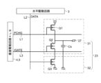
- FIG. 4 is a circuit diagram of the pixel circuit 23 according to the first specific example.
- the pixel circuit 23 in FIG. 4 includes a capacitor Cs, a charging/discharging circuit 31, and a control circuit 32.
- the capacitor Cs holds a charge corresponding to the voltage supplied to the display element.
- the display element is, for example, a liquid crystal element, and one end of the capacitor Cs is connected to a pixel electrode 27 that applies a voltage to the liquid crystal element.
- the charging/discharging circuit 31 charges and discharges the capacitor Cs. Since a voltage corresponding to the charge of the capacitor Cs is applied to the pixel electrode 27, the charging/discharging circuit 31 may be referred to as a pixel electrode drive circuit 31 below.
- the pixel electrode drive circuit 31 in FIG. 4 includes two medium/high voltage NMOS transistors (a first switching element Q1 and a second switching element Q2).
- the first switching element Q1 may be referred to as an NMOS transistor Q1
- the second switching element Q2 may be referred to as an NMOS transistor Q2.
- the control circuit 32 controls the pixel electrode drive circuit 31. More specifically, the control circuit 32 generates a control signal for controlling the pixel electrode drive circuit 31.
- the control circuit 32 in FIG. 4 includes a plurality of low voltage transistors Q3 to Q6. Since the voltage amplitude of each signal input to or output from the control circuit 32 is smaller than the voltage amplitude applied to the liquid crystal element and the drive circuit for the liquid crystal element, the pixel circuit 23 in FIG. 4 uses a plurality of control circuits 32. It consists of low voltage transistors.
- the control circuit 32 is sometimes called a logic circuit.
- the pixel circuit 23 in FIG. 4 is configured using medium/high voltage MOS transistors Q1 and Q2 and low voltage MOS transistors Q3 to Q6.
- the circuit area and power consumption can be reduced compared to the case where all the transistors are made to have medium/high breakdown voltages as in the pixel circuit 23 of FIG. 3.
- FIG. 4 shows an example in which the control circuit 32 performs a NOR operation, the type of logical operation performed by the control circuit 32 does not matter.
- the control circuit 32 in FIG. 4 has four low-voltage transistors Q3 to Q6, the number of transistors in the control circuit 32 is also arbitrary. Further, the control circuit 32 in FIG. 4 has two PMOS transistors Q3 and Q4 and two NMOS transistors Q5 and Q6, but the conductivity types of the transistors are arbitrary. Further, although FIG. 4 shows an example in which the control circuit 32 includes four MOS transistors Q3 to Q6, it may be configured with bipolar transistors or Bi-CMOS transistors.
- the control circuit 32 includes two PMOS transistors Q3 and Q4 connected in cascode between a first power supply voltage node VDD and an output node CTout of the control circuit 32, and a transistor connected between the output node CTout of the control circuit 32 and a ground node Vss. and an NMOS transistor Q6 connected between the output node CTout of the control circuit 32 and the ground node Vss.
- Pixel data DATA output from the horizontal drive circuit 3 via the data line L2 is input to the gate of the PMOS transistor Q3 and the gate of the NMOS transistor Q5.
- a gate signal /GATE outputted from the vertical drive circuit 4 via the gate line L3 is input to the gate of the PMOS transistor and the gate of the NMOS transistor.
- Gate signal /GATE is a display timing signal.
- the control circuit 32 in FIG. 4 receives the pixel data DATA output from the horizontal drive circuit 3 via the data line L2 and the gate signal /GATE (more precisely, A control signal is generated by performing a NOR operation with the inverted signal of the gate signal GATE.
- the control circuit 32 outputs a high level control signal CTout when the pixel data DATA is at a low level and the inverted signal of the gate signal /GATE is at a low level.
- a low level control signal CTout is output.
- the pixel electrode drive circuit 31 has two medium/high voltage NMOS transistors Q1 and Q2.
- NMOS transistor Q1 and NMOS transistor Q2 are cascode-connected between second power supply voltage node VH and ground node Vss.
- the second power supply voltage node VH is a node having a higher voltage level than the first power supply voltage node VDD.
- the pixel electrode drive circuit 31 includes a capacitor Cs connected between the connection node of the NMOS transistor Q1 and the NMOS transistor Q2 (the node connected to the pixel electrode 27) and the ground node Vss.
- This capacitor Cs functions as a memory 24 that stores pixel data DATA.
- a precharge signal PCHG outputted from the vertical drive circuit 4 via the precharge signal line L1 is input to the gate of the NMOS transistor Q1.
- Precharge signal PCHG has a voltage amplitude larger than the voltage amplitude of control circuit 32. More specifically, precharge signal PCHG has a voltage amplitude between the ground voltage (0V) and (5V+Vth). Vth is the threshold voltage of the NMOS transistor Q1.
- the precharge signal PCHG becomes high level (5V+Vth)
- the NMOS transistor Q1 is turned on, the source of the NMOS transistor Q1 becomes 5V, and the capacitor Cs is charged with 5V.
- the charging voltage of the capacitor Cs becomes a voltage lower than the high level voltage of the precharge signal PCHG by the threshold voltage of the NMOS transistor Q1. Therefore, the voltage level of the precharge signal PCHG needs to be set in consideration of the fact that the voltage at one end of the capacitor Cs is lower by the threshold voltage of the NMOS transistor Q1.
- a control signal CTout output from the control circuit 32 is input to the gate of the NMOS transistor Q2.
- the voltage amplitude of the control signal CTout is smaller than the voltage amplitude of the precharge signal PCHG, but since the voltage amplitude of the drain of the NMOS transistor Q2 is larger than the voltage amplitude of the control circuit 32, the NMOS transistor Q2 is a medium/high voltage transistor. It consists of
- the circuit area is larger than that of two low voltage NMOS transistors, but as shown in FIG. Compared to making all MOS transistors in the pixel circuit 23 medium/high withstand voltage, the circuit area is much smaller and the power consumption can be reduced.
- the pixel circuit 23 in FIG. 4 stores pixel data DATA in the capacitor Cs instead of the memory 24 in FIG. 3.
- the memory 24 in FIG. 3 has an SRAM configuration and requires six MOS transistors.
- the pixel circuit 23 in FIG. 4 can store pixel data DATA with only one capacitor Cs.
- a control circuit 32 for generating a control signal CTout for controlling the pixel electrode drive circuit 31 is required.
- the total number of transistors is the same, six, but the pixel circuit 23 in FIG. In the pixel circuit 23 of No. 4, only two transistors have medium/high breakdown voltage, and four transistors have low breakdown voltage. Therefore, although the pixel circuit 23 in FIG. 4 requires a capacitor Cs, it can be realized with a smaller circuit area than the pixel circuit 23 in FIG.
- the capacitor Cs is charged and the pixel electrode 27 is driven.
- a voltage lower than the voltage level of the precharge signal PCHG input to the gate of the NMOS transistor Q1 by the threshold voltage of the NMOS transistor Q1 is applied to one end of the capacitor Cs and the pixel electrode. 27. Therefore, in order to prevent the voltage drop by the threshold voltage from occurring, it is necessary to increase the voltage level of the precharge signal PCHG by the threshold voltage.
- the pixel circuit 23 in FIG. 4 can have a smaller circuit area than the pixel circuit 23 in FIG. 3. More specifically, in the pixel circuit 23 of FIG. 4, the pixel electrode drive circuit 31, for which miniaturization of design rules is difficult, is configured with two medium/high voltage MOS transistors, and a control circuit that controls the pixel electrode drive circuit 31 is configured. Since 32 is composed of low voltage MOS transistors, the number of medium/high voltage transistors can be minimized and the circuit area can be reduced.
- the two MOS transistors Q1 and Q2 in the pixel electrode drive circuit 31 have the same conductivity type.
- a single conductivity type well region for example, a P well region in the case of an NMOS transistor
- the pixel circuit 23 in FIG. 4 does not require the two NMOS transistors 25 and 26 in FIG. 3 that switch and control whether or not to write pixel data DATA to the pixel electrode 27.
- the pixel electrode drive circuit 31 is controlled by the control circuit 32 made up of low-voltage transistors, so that power consumption can be reduced.
- the control circuit 32 in the pixel circuit 23 in FIG. 4 controls whether or not to capture pixel data DATA from the horizontal drive circuit 3, controls whether or not to store pixel data DATA in the capacitor Cs, and performs simple Perform level shift.
- the pixel circuit 23 in FIG. 4 can lower the voltage amplitude of the pixel data DATA outputted from the horizontal drive circuit 3 via the data line L2 to the voltage amplitude of the control circuit 32, thereby reducing power consumption.
- the pixel data DATA output from the horizontal drive circuit 3 via the data line L2 is input to the gates of medium or medium/high voltage transistors Q1 and Q2. It is necessary to increase the voltage amplitude of the pixel data DATA on the data line L2, which increases power consumption.
- the pixel circuit 23 in FIG. 4 can be configured with a smaller circuit area and lower power consumption than the pixel circuit 23 in FIG. 3.
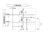
- FIG. 5 is a circuit diagram of the pixel circuit 23 according to the second specific example.
- the configuration of the control circuit 32 is simplified compared to the pixel circuit 23 of FIG.
- the pixel circuit 23 in FIG. 5 includes three medium/high voltage NMOS transistors Q1 to Q3 and a capacitor Cs. These three NMOS transistors Q1 to Q3 are connected in cascode between the second power supply voltage node VH and the ground node Vss.
- a precharge signal PCHG output from the vertical drive circuit 4 is input to the gate of the NMOS transistor Q1.
- the NMOS transistor Q1 and the NMOS transistor Q2 constitute a charge/discharge circuit 31 (pixel electrode drive circuit 31), and the NMOS transistor Q3 constitutes a control circuit 32.
- NMOS transistor Q3 also functions as a charging/discharging circuit 31.
- the precharge signal PCHG is set to a voltage level higher than the charging voltage of the capacitor Cs by the threshold voltage of the NMOS transistor Q1.
- the control circuit 32 in the pixel circuit 23 in FIG. 4 is composed of low voltage MOS transistors Q3 to Q6, but the control circuit 32 in the pixel circuit 23 in FIG. 5 is composed of a medium/high voltage MOS transistor Q3. It is configured.
- the capacitor Cs is connected between the connection node between the NMOS transistor Q1 and the NMOS transistor Q2 (the node connected to the pixel electrode 27) and the ground node Vss. That is, the capacitor Cs is connected between the drain of the NMOS transistor Q2 and the ground node Vss.
- This capacitor Cs holds charge according to pixel data DATA. That is, this capacitor Cs is used to store pixel data DATA.
- a gate signal /GATE outputted from the vertical drive circuit 4 via the gate line L3 is input to the gate of the NMOS transistor Q2.
- Pixel data DATA output from the horizontal drive circuit 3 via the data line L2 is input to the gate of the NMOS transistor Q3.
- the voltage amplitude of the gate signal /GATE output from the vertical drive circuit 4 was low, but in the pixel circuit 23 in FIG.
- the voltage amplitude of GATE is made larger than the logic circuit level. The reason is that the drain of the NMOS transistor Q2 is connected to the pixel electrode 27 and has a high voltage level.
- the voltage amplitude of the pixel data DATA output from the horizontal drive circuit 3 via the data line L2 is set to a low amplitude.
- Pixel data DATA is input to the gate of NMOS transistor Q1.
- the NMOS transistor Q1 is made into a medium/high voltage transistor.
- the pixel circuit 23 in FIG. 5 is composed of only the three medium/high voltage MOS transistors Q1 to Q3 and the capacitor Cs, the circuit area can be reduced compared to the pixel circuit 23 in FIG. 4.
- the voltage amplitudes of the precharge signal PCHG and the gate signal /GATE output from the vertical drive circuit 4 are larger than the voltage amplitude of the control circuit 32, the power consumption of the vertical drive circuit 4 in FIG.
- the number of drive circuits is greater than that of drive circuit 4.
- the three transistors Q1 to Q3 in the pixel circuit 23 in FIG. 5 are all of the same conductivity type, only the P-well region needs to be provided when a bulk structure is used, and the circuit area can be further reduced.
- FIG. 6 is a circuit diagram of the pixel circuit 23 according to the third specific example.
- the pixel circuit 23 in FIG. 6 includes a charge/discharge circuit 31 (pixel electrode drive circuit 31) and a control circuit 32.
- the control circuit 32 includes a low voltage NMOS transistor Q3.
- the pixel electrode drive circuit 31 includes two medium/high voltage NMOS transistors (NMOS transistor Q1 and NMOS transistor Q2) and a capacitor Cs.
- the first, second, and third NMOS transistors Q1 to Q3 are cascode-connected between the second power supply voltage node VH and the ground node Vss.
- the pixel circuit 23 in FIG. 6 is different in that the NMOS transistor Q1 in the pixel circuit 23 in FIG. 5 has a lower breakdown voltage, but the circuit configuration is the same.
- the voltage amplitude of the gate signal /GATE from the vertical drive circuit 4 that is input to the gate of the NMOS transistor Q2 in the pixel circuit 23 in FIG. 6 is approximately the same as the voltage amplitude of the control circuit 32. More specifically, the high level of the gate signal /GATE is a voltage level higher than the high level voltage of the control circuit 32 by the threshold voltage of the NMOS transistor Q2.
- the NMOS transistor Q1 is turned into a low voltage MOS transistor. can do.
- the pixel circuit 23 in FIG. 6 is composed of two medium/high voltage transistors Q1 and Q2, one low voltage transistor Q3, and a capacitor Cs, so it has a larger circuit area than the pixel circuit 23 in FIG. It can be reduced.
- the circuit area can be further reduced.
- the voltage level of the precharge signal PCHG input to the gates of the MOS transistors Q1 and Q2 in the pixel electrode drive circuit 31 used to charge the capacitor Cs is higher than that of the precharge signal PCHG. Since a voltage lower by the threshold voltage is supplied to one end of the capacitor Cs and the pixel electrode 27, voltage efficiency cannot be said to be good.
- a pixel circuit 23 according to a fourth specific example described below is configured such that a voltage at the same voltage level as the precharge signal PCHG is supplied to one end of the capacitor Cs and the pixel electrode 27.
- FIG. 7 is a circuit diagram of the pixel circuit 23 according to the fourth specific example.
- the pixel circuit 23 in FIG. 7 includes a control circuit 32 and a pixel electrode drive circuit 31.
- the control circuit 32 in FIG. 7 has a similar circuit configuration to the control circuit 32 in FIG. 4. Specifically, the control circuit 32 in FIG. 7 includes four low voltage MOS transistors Q3 to Q6. More specifically, the control circuit 32 in FIG. 7 includes two PMOS transistors (PMOS transistor Q3 and PMOS transistor Q4) and two NMOS transistors Q5 and Q6. These four low voltage MOS transistors Q3 to Q6 constitute, for example, a NOR circuit.
- PMOS transistor Q3, PMOS transistor Q4, and NMOS transistor Q5 are cascode-connected between the first power supply voltage node VDD and the ground node Vss.
- the drain of the NMOS transistor Q5 and the drain of the NMOS transistor Q6 are connected to the output node CTout of the control circuit 32.
- the source of NMOS transistor Q5 and the source of NMOS transistor Q6 are connected to ground node Vss.
- Pixel data DATA is input to the gate of the PMOS transistor Q3 and the gate of the NMOS transistor Q5.
- a gate signal /GATE is input to the gate of the PMOS transistor Q4 and the gate of the NMOS transistor Q6.
- the pixel electrode drive circuit 31 in FIG. 7 includes four medium/high voltage NMOS transistors Q1, Q2, Q7, and Q8, and three capacitors (first to third capacitors) C1 to C3.
- the second capacitor C2 functions as a capacitor Cs that holds charge according to the voltage applied to the pixel electrode 27.
- the first capacitor C1, the third capacitor C3, and the NMOS transistor Q8 constitute a compensation circuit 33.
- the compensation circuit 33 compensates for a drop in the charging voltage of the second capacitor C2 caused by the precharge signal PCHG being input to the gate of the NMOS transistor Q1 via a diode or a diode-connected NMOS transistor Q7.
- An NMOS transistor Q1 and an NMOS transistor Q2 are connected in cascode between the second power supply voltage node VH and the ground node Vss.
- a control signal CTout output from the control circuit 32 is input to the gate of the NMOS transistor Q2.
- a diode-connected NMOS transistor Q7 is connected to the gate of the NMOS transistor Q1.
- a precharge signal PCHG from the vertical drive circuit 4 is input to the gate and source of the NMOS transistor Q7.
- An NMOS transistor Q8 is connected between the gate of the NMOS transistor Q1 and the ground node Vss.
- a first capacitor C1 and a second capacitor C2 are connected in series between the gate of the NMOS transistor Q1 and the ground node Vss. One end of the second capacitor C2 is connected to the pixel electrode 27.
- a third capacitor C3 is connected between one end of the second capacitor C2 and the gate of the NMOS transistor Q8.
- the gate of the NMOS transistor Q1 is referred to as a first node n1
- one end of the second capacitor C2 is referred to as a second node n2
- the gate and source of the NMOS transistor Q7 are referred to as a third node n3
- the gate of the NMOS transistor Q8 is referred to as a fourth node n4. call.
- a diode-connected NMOS transistor Q7 is connected to the first node n1. Therefore, when the voltage of the first node n1 is higher than the voltage of the precharge signal PCHG, the first node n1 and the third node n3 can be electrically isolated, and the voltage level of the first node n1 can be changed to the precharge signal PCHG. It can be set higher than the voltage level of charge signal PCHG.
- the NMOS transistor Q1 When the precharge signal PCHG becomes high level, the NMOS transistor Q1 is turned on, and a charge corresponding to the threshold voltage of the NMOS transistor Q1 is held in the first capacitor C1. Therefore, a charge corresponding to a voltage lower than the voltage level of the precharge signal PCHG by the threshold voltage is held in the second capacitor C2.
- An inverted signal of the precharge signal PCHG is input to the gate of the NMOS transistor Q8. Therefore, when the precharge signal PCHG is at a high level, the gate of the NMOS transistor Q8 is at the ground level, and a charge equivalent to that of the second capacitor C2 is held.
- the NMOS transistor Q1 When the precharge signal PCHG becomes low level, the NMOS transistor Q1 is turned off. Since the inverted signal of the precharge signal PCHG is input to the gate of the NMOS transistor Q8, it becomes high level. Therefore, the voltage level of the second node n2 becomes high, and the voltage applied to the pixel electrode 27 becomes approximately the same voltage level as the high level of the precharge signal PCHG.
- the first capacitor C1 in order to compensate for the fact that a voltage lower than the high level of the precharge signal PCHG by the threshold voltage of the NMOS transistor Q1 is applied to the pixel electrode 27, the first capacitor C1, A voltage comparable to the high level of the precharge signal PCHG can be applied to the pixel electrode 27 by the bootslap-configured circuit including the third capacitor C3, the diode-connected NMOS transistor Q7, and the NMOS transistor Q8.
- the pixel circuit 23 in order to apply a voltage at the same level as the power supply voltage to the pixel electrode 27, it is necessary to make the high level of the precharge signal PCHG higher than the power supply voltage by the threshold voltage of the MOS transistor. Therefore, it was necessary to generate the precharge signal PCHG at a voltage level higher than the power supply voltage.
- the pixel circuit 23 according to the fourth specific example even if the high level of the precharge signal PCHG is set to the same level as the power supply voltage, a voltage at the same level as the power supply voltage can be applied to the pixel electrode 27, and the power supply voltage can be applied to the pixel electrode 27. It is not necessary to generate the precharge signal PCHG at a voltage level higher than the voltage level. Thereby, the circuit configuration of the vertical drive circuit 4 can be simplified.
- FIG. 8 is a circuit diagram of the pixel circuit 23 according to the fifth specific example.
- the pixel circuit 23 in FIG. 8 includes a control circuit 32 and a charge/discharge circuit (pixel electrode drive circuit) 31.
- the pixel circuit 23 in FIG. 8 is obtained by changing the ground node Vss of the pixel circuit 23 in FIG. 4 to a negative power supply voltage node (-VDD). That is, a positive power supply voltage node VDD and a negative power supply voltage node (-VDD) are connected to the control circuit 32 and the pixel electrode drive circuit 31 in the pixel circuit 23 in FIG.
- the pixel electrode drive circuit 31 includes a PMOS transistor Q11 and an NMOS transistor Q12 connected in cascode between a positive power supply voltage node VDD and a negative power supply voltage node (-VDD), and a capacitor Cs.
- a precharge signal PCHG having a voltage amplitude between the positive power supply voltage VDD and the ground voltage Vss is input to the gate of the PMOS transistor Q11.
- a control signal CTout output from the control circuit 32 is input to the gate of the NMOS transistor Q12.
- Precharge signal PCHG is input from vertical drive circuit 4.
- the PMOS transistor Q11 When the precharge signal PCHG falls to the ground voltage Vss, the PMOS transistor Q11 is turned on and the capacitor Cs is charged. The capacitor Cs holds a charge corresponding to a voltage twice the power supply voltage VDD.
- the control signal CTout becomes a high level ground voltage, the NMOS transistor Q12 is turned on and the accumulated charge in the capacitor Cs is discharged.
- the control circuit 32 has two PMOS transistors Q13 and Q14 and two NMOS transistors Q15 and Q16 that constitute a NOR circuit.
- a ground node Vss is connected to the source of the PMOS transistor Q13.
- the source of NMOS transistor Q15 and the source of NMOS transistor Q16 are connected to a negative power supply voltage node (-VDD).
- Pixel data DATA from the horizontal drive circuit 3 and gate signal /GATE from the vertical drive circuit 4 are input to the control circuit 32 .
- the pixel data DATA has a voltage amplitude between the ground voltage Vss and the negative power supply voltage (-VDD).
- the gate signal /GATE has a voltage amplitude between the ground voltage Vss and the negative power supply voltage (-VDD).
- the pixel circuit 23 in FIG. 8 uses the positive power supply voltage VDD and the negative power supply voltage (-VDD) to hold a charge in the capacitor Cs corresponding to twice the power supply voltage. This eliminates the problem that a voltage lower than the voltage level of the precharge signal PCHG is applied to the pixel electrode 27.
- FIG. 9 is a circuit diagram of the pixel circuit 23 according to the sixth specific example.
- the pixel circuit 23 in FIG. 9 has the conductivity types of two MOS transistors constituting the charge/discharge circuit (pixel electrode drive circuit) 31 in the pixel circuit 23 in FIG. 4 reversed.
- the pixel circuit 23 in FIG. 9 has a pixel electrode drive circuit 31 and a control circuit 32.
- the pixel electrode drive circuit 31 in FIG. 9 has two PMOS transistors Q21 and Q22.
- the source of the PMOS transistor Q21 is connected to the power supply voltage VH node, and the control signal CTout from the control circuit 32 is input to the gate of the PMOS transistor Q21.
- the source of the PMOS transistor Q22 is connected to the drain of the PMOS transistor Q21, and the precharge signal PCHG is input to the gate of the PMOS transistor Q22.
- the drain of PMOS transistor Q22 is connected to ground node Vss.
- Capacitor Cs is connected between the source of PMOS transistor Q22 and ground node Vss.
- the control circuit 32 has two PMOS transistors Q23 and Q24 and two NMOS transistors Q25 and Q26 that constitute a NOR circuit.
- the source of the PMOS transistor Q23 is connected to the power supply node VH, and the pixel data DATA is input to the gate of the PMOS transistor Q23.
- Pixel data DATA has a voltage amplitude of VH and VH-VDD.
- the source of the PMOS transistor Q24 is connected to the drain of the PMOS transistor Q23, and the gate signal /GATE is input to the gate of the PMOS transistor Q24.
- the drain of the NMOS transistor Q25 is connected to the drain of the PMOS transistor Q24 (output node CTout of the control circuit 32), and the pixel data DATA is input to the gate of the NMOS transistor Q25.
- the drain of the NMOS transistor Q26 is connected to the output node CTout of the control circuit 32, and the gate signal /GATE is input to the gate of the NMOS transistor Q26.
- the source of the NMOS transistor Q25 and the source of the NMOS transistor Q26 are connected to a power supply voltage (VH-VDD) node. As a result, the voltage amplitude of the control signal CTout output from the control circuit 32 becomes VH and VH-VDD.
- the PMOS transistor Q21 is turned on when the control signal CTout output from the control circuit 32 is VH-VDD, and the capacitor Cs holds a charge corresponding to the power supply voltage VH. Further, when the precharge signal PCHG is VH-Vth, the PMOS transistor Q22 is turned on, and the accumulated charge in the capacitor Cs is discharged.
- the pixel circuits 23 have a charging/discharging circuit 31, a control circuit 32, and a capacitor Cs as common circuit configurations.
- the charging/discharging circuit 31 charges and discharges the capacitor Cs.
- the control circuit 32 controls the charging/discharging circuit 31.
- the charging/discharging circuit 31 includes a first switching element Q1 that controls charging of the capacitor Cs, and a second switching element Q2 that controls discharging of the capacitor Cs.
- the control circuit 32 includes a third switching element Q3 that controls on or off of at least one of the first switching element Q1 and the second switching element Q2 based on at least one of the pixel data DATA and the display timing signal.
- the first switching element Q1 is, for example, the NMOS transistor Q1 in FIG. 4.
- the second switching element Q2 is, for example, the NMOS transistor Q2 shown in FIG.
- the third switching elements are, for example, NMOS transistors Q3 to Q6 in FIG. 4.
- the circuit area can be reduced and the consumption Power consumption can be reduced.
- the conductivity types of the first switching element Q1 and the second switching element Q2 in the charge/discharge circuit (pixel electrode drive circuit) 31 the same, only a single-polarity well region can be provided in the case of a bulk structure. This makes it possible to further reduce the circuit area.
- Each transistor in the pixel circuit 23 according to the first to fifth specific examples may be a MOS transistor or a bipolar transistor.
- FIG. 10A is a diagram showing the interior of the vehicle 100 from the rear to the front of the vehicle 100
- FIG. 10B is a diagram showing the interior of the vehicle 100 from the diagonal rear to the diagonal front of the vehicle 100.
- the vehicle 100 of FIGS. 10A and 10B includes a center display 101, a console display 102, a head-up display 103, a digital rear mirror 104, a steering wheel display 105, and a rear entertainment display 106.
- the center display 101 is placed on the dashboard 107 at a location facing the driver's seat 108 and passenger seat 109.
- FIG. 10 shows an example of a horizontally long center display 101 extending from the driver's seat 108 side to the passenger seat 109 side
- the screen size and placement location of the center display 101 are arbitrary.
- Center display 101 can display information detected by various sensors. As a specific example, the center display 101 displays images taken by an image sensor, distance images to obstacles in front and on the side of the vehicle measured by a ToF sensor, and passenger body temperature detected by an infrared sensor. Can be displayed.
- the center display 101 can be used to display at least one of safety-related information, operation-related information, life log, health-related information, authentication/identification-related information, and entertainment-related information, for example.
- Safety-related information includes information such as detection of falling asleep, detection of looking away, detection of mischief by children in the same vehicle, presence or absence of seatbelts, and detection of leaving passengers behind. This information is detected by The operation-related information uses sensors to detect gestures related to operations by the occupant.
- the detected gestures may include manipulation of various equipment within the vehicle 100. For example, the operation of air conditioning equipment, navigation equipment, AV equipment, lighting equipment, etc. is detected.
- the life log includes life logs of all crew members. For example, a life log includes a record of the actions of each occupant during the ride. By acquiring and saving life logs, it is possible to check the condition of the occupants at the time of the accident.
- a temperature sensor is used to detect the occupant's body temperature, and the occupant's health condition is estimated based on the detected body temperature.
- an image sensor may be used to capture an image of the occupant's face, and the occupant's health condition may be estimated from the captured facial expression.
- Authentication/identification related information includes a keyless entry function that performs facial recognition using a sensor, and a function that automatically adjusts seat height and position using facial recognition.
- the entertainment-related information includes a function that uses a sensor to detect operation information of an AV device by a passenger, a function that recognizes the passenger's face using a sensor, and provides the AV device with content suitable for the passenger.
- the console display 102 can be used, for example, to display life log information.
- the console display 102 is arranged near a shift lever 111 on a center console 110 between a driver's seat 108 and a passenger seat 109.
- the console display 102 can also display information detected by various sensors. Further, the console display 102 may display an image around the vehicle captured by an image sensor, or may display a distance image to an obstacle around the vehicle.
- the head-up display 103 is virtually displayed behind the windshield 112 in front of the driver's seat 108.
- the head-up display 103 can be used, for example, to display at least one of safety-related information, operation-related information, life log, health-related information, authentication/identification-related information, and entertainment-related information. Since the head-up display 103 is often placed virtually in front of the driver's seat 108, it is difficult to display information directly related to the operation of the vehicle 100, such as the speed of the vehicle 100 and the remaining amount of fuel (battery). Are suitable.
- the digital rear mirror 104 can display not only the rear of the vehicle 100 but also the state of the occupants in the rear seats. Therefore, by arranging a sensor on the back side of the digital rear mirror 104, it can be used for displaying life log information, for example. be able to.
- the steering wheel display 105 is placed near the center of the steering wheel 113 of the vehicle 100.
- Steering wheel display 105 can be used, for example, to display at least one of safety-related information, operation-related information, life log, health-related information, authentication/identification-related information, and entertainment-related information.
- life log information such as the driver's body temperature, information regarding the operation of AV equipment, air conditioning equipment, etc. There is.
- the rear entertainment display 106 is attached to the back side of the driver's seat 108 and the passenger seat 109, and is for viewing by passengers in the rear seats.
- the rear entertainment display 106 can be used, for example, to display at least one of safety-related information, operation-related information, lifelog, health-related information, authentication/identification-related information, and entertainment-related information.
- information relevant to the rear seat occupant is displayed. For example, information regarding the operation of the AV device or air conditioning equipment may be displayed, or the results of measuring the body temperature of the passenger in the rear seat using a temperature sensor may be displayed.
- optical distance measurement methods There are two main types of optical distance measurement methods: passive and active.
- a passive type sensor measures distance by receiving light from an object without emitting light from the sensor to the object.
- Passive methods include the lens focusing method, stereo method, and monocular viewing method.
- the active type measures distance by projecting light onto an object and receiving the reflected light from the object with a sensor.
- Active types include an optical radar method, an active stereo method, a photometric stereo method, a moiré topography method, and an interferometry method.
- the display device 1 according to the present disclosure is applicable to any of these methods of distance measurement. By using the sensors stacked on the back side of the display device 1 according to the present disclosure, the above-described passive or active distance measurement can be performed.
- the display device 1 according to the present disclosure is applicable not only to various displays used in vehicles, but also to displays mounted on various electronic devices 50.
- FIG. 11A is a front view of a digital camera 120, which is a second application example of the electronic device 50, and FIG. 11B is a rear view of the digital camera 120.
- the digital camera 120 in FIGS. 11A and 11B is an example of a single-lens reflex camera in which the lens 121 is replaceable, the digital camera 120 is also applicable to a camera in which the lens 121 is not replaceable.
- FIGS. 11A and 11B when the photographer looks through the electronic viewfinder 124 while holding the grip 123 of the camera body 122, decides on the composition, adjusts the focus, and presses the shutter 125, the camera The shooting data is saved in the memory of the camera.
- a monitor screen 126 for displaying shooting data, live images, etc., and an electronic viewfinder 124 are provided on the back side of the camera.
- a sub-screen that displays setting information such as shutter speed and exposure value may be provided on the top surface of the camera.
- the display device 1 By arranging a sensor overlapping the back side of the monitor screen 126, electronic viewfinder 124, sub-screen, etc. used in the camera, it can be used as the display device 1 according to the present disclosure.
- the display device 1 according to the present disclosure is also applicable to a head mounted display (hereinafter referred to as HMD).
- HMDs can be used for VR (Virtual Reality), AR (Augmented Reality), MR (Mixed Reality), SR (Substitutional Reality), and the like.
- FIG. 12A is an external view of an HMD 130 that is a third application example of the electronic device 50.
- the HMD 130 in FIG. 12A has a mounting member 131 that is worn to cover a human's eyes. This mounting member 131 is fixed by being hooked onto a human ear, for example.
- a display device 132 is provided inside the HMD 130, and the wearer of the HMD 130 can view stereoscopic images and the like on this display device 132.
- the HMD 130 includes, for example, a wireless communication function and an acceleration sensor, and can switch the stereoscopic image displayed on the display device 132 according to the wearer's posture, gestures, and the like.
- a camera may be provided in the HMD 130 to take images of the surroundings of the wearer, and an image obtained by combining the image taken by the camera and an image generated by a computer may be displayed on the display device 132.
- a camera is placed on the back side of the display device 132 that is visible to the wearer of the HMD 130, and the camera takes pictures of the area around the eyes of the wearer, and the captured image is sent to another camera provided on the outer surface of the HMD 130.
- the display device 1 can also be applied to smart glasses 130a that display various information on glasses 134.
- Smart glasses 130a in FIG. 12B include a main body portion 135, an arm portion 136, and a lens barrel portion 137.
- the main body portion 135 is connected to an arm portion 136.
- the main body portion 135 is attachable to and detachable from the glasses 134.
- the main body section 135 includes a control board and a display section for controlling the operation of the smart glasses 130a.
- the main body part 135 and the lens barrel part 137 are connected to each other via an arm part 136.
- the lens barrel section 137 emits the image light emitted from the main body section 135 via the arm section 136 to the lens 138 side of the glasses 134 .
- This image light enters the human eye through lens 138.
- the wearer of the smart glasses 130a in FIG. 12B can visually recognize not only the surrounding situation but also various information emitted from the lens barrel section 137, just like normal glasses.
- the display device 1 according to the present disclosure is also applicable to a television device (hereinafter referred to as TV).
- TV television device
- Recent TVs tend to have frame sizes as small as possible from the viewpoint of miniaturization and aesthetic design. For this reason, when a TV is provided with a camera that photographs the viewer, it is desirable to place the camera on the back side of the display panel of the TV.
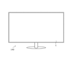
- FIG. 13 is an external view of a TV 140 that is a fourth application example of the electronic device 50.
- the TV 140 in FIG. 13 has a minimized frame, and almost the entire front side is the display area.
- the TV 140 may have a built-in sensor such as a camera for photographing the viewer.
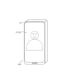
- FIG. 14 is an external view of a smartphone 150 that is a fifth application example of the electronic device 50.
- the display surface 1z extends to nearly the external size of the electronic device 50, and the width of the bezel 1y around the display surface 1z is set to several mm or less.
- a front camera is often mounted on the bezel 1y, but an image sensor module functioning as a front camera may be arranged, for example, on the back side of the display surface 1z at approximately the center.
- the present technology can have the following configuration.
- the pixel includes a display element and a pixel circuit that controls a voltage supplied to the display element,
- the pixel circuit is a capacitor that holds charge according to the voltage supplied to the display element; a charging/discharging circuit that charges and discharges the capacitor; a control circuit that controls the charging and discharging circuit;
- the charging/discharging circuit is a first switching element that controls charging of the capacitor; a second switching element that controls discharge of the capacitor;
- a display device wherein the control circuit includes a third switching element that controls on or off of at least one of the first switching element and the second switching element based on at least one of pixel data or a display timing signal.
- the first switching element and the second switching element have the same breakdown voltage and the same conductivity type.
- the first switching element and the second switching element in the charging/discharging circuit have a first breakdown voltage;
- the third switching element in the control circuit has a second breakdown voltage lower than the first breakdown voltage.
- the first switching element, the second switching element, and the third switching element are cascode-connected between a first reference voltage node and a second reference voltage node;
- the display device according to (1) or (2), wherein the capacitor is connected between a connection node between the first switching element and the second switching element and the second reference voltage node.
- the display device wherein the third switching element has the same breakdown voltage and the same conductivity type as the first switching element and the second switching element.
- the third switching element has a different breakdown voltage and the same conductivity type as the first switching element and the second switching element.
- the first switching element and the second switching element are cascode-connected between a first reference voltage node and a second reference voltage node;
- the display according to any one of (1) to (3), wherein the capacitor is connected between a connection node of the first switching element and the second switching element and the second reference voltage node.
- the control circuit generates a control signal to be input to a gate of at least one of the first switching element and the second switching element, based on the pixel data and the display timing signal.
- the display device according to any one of (7).
- the precharge signal is input to the gate of either the first switching element or the second switching element, and the control signal is input to the other gate.
- Display device (10) The display device according to (9), wherein the voltage amplitude of the precharge signal is larger than the voltage amplitude of the control signal.
- (11) The display device according to (9) or (10), wherein the voltage amplitude of the precharge signal is larger than the voltage amplitudes of the pixel data and the display timing signal.
- the first switching element and the second switching element are N-type MOS (Metal Oxide Semiconductor) transistors,
- the drain of the first switching element is connected to a first reference voltage node, one end of the capacitor is connected to the source of the first switching element,
- the first drive circuit adjusts the voltage level of the precharge signal to the first reference voltage node so that the source of the first switching element has the same voltage level as the first reference voltage node when charging the capacitor.
- the first switching element and the second switching element are P-type MOS (Metal Oxide Semiconductor) transistors,
- the source of the first switching element is connected to a first reference voltage node
- the drain of the second switching element is connected to a second reference voltage node
- one end of the capacitor is connected to the drain of the first switching element
- the first drive circuit adjusts the voltage level of the precharge signal to the second reference voltage node so that the drain of the first switching element becomes the same voltage level as the second reference voltage node when the capacitor is discharged.
- the display device according to (12) wherein the voltage is set to be lower than the voltage by the threshold voltage.
- the first drive circuit outputs the precharge signal having a voltage amplitude larger than the voltage amplitude of the control circuit and the display timing signal having a voltage amplitude comparable to the voltage amplitude of the control circuit.
- the display device according to any one of (12) to (14), which is input to a control circuit.
- the charging/discharging circuit is a diode or a diode-connected transistor connected to the gate of the first switching element; (9) comprising a compensation circuit that compensates for a decrease in the charging voltage of the capacitor caused by inputting the precharge signal to the gate of the first switching element via the diode or the diode-connected transistor;
- the display device according to any one of (11) to (11).
- the first reference voltage of the first reference voltage node and the second reference voltage of the second reference voltage node are voltages with opposite voltage polarities
- the precharge signal supplied to the gate of the first switching element and the pixel data have opposite voltage polarities;
- the display device according to (17), wherein the control circuit is supplied with the first reference voltage or the second reference voltage, and an intermediate voltage between the first reference voltage and the second reference voltage.
- the display device according to (16) or (17), wherein the first switching element and the second switching element have the same breakdown voltage and different conductivity types.
Landscapes
- Physics & Mathematics (AREA)
- Nonlinear Science (AREA)
- Engineering & Computer Science (AREA)
- General Physics & Mathematics (AREA)
- Chemical & Material Sciences (AREA)
- Crystallography & Structural Chemistry (AREA)
- Optics & Photonics (AREA)
- Mathematical Physics (AREA)
- Microelectronics & Electronic Packaging (AREA)
- Theoretical Computer Science (AREA)
- Power Engineering (AREA)
- Computer Hardware Design (AREA)
- Control Of Indicators Other Than Cathode Ray Tubes (AREA)
- Liquid Crystal Display Device Control (AREA)
Abstract
Description
前記画素は、表示素子と、前記表示素子に供給される電圧を制御する画素回路と、を有し、
前記画素回路は、
前記表示素子に供給される電圧に応じた電荷を保持するキャパシタと、
前記キャパシタの充放電を行う充放電回路と、
前記充放電回路を制御する制御回路と、を有し、
前記充放電回路は、
前記キャパシタの充電を制御する第1スイッチング素子と、
前記キャパシタの放電を制御する第2スイッチング素子と、を有し、
前記制御回路は、画素データ又は表示タイミング信号の少なくとも一方に基づいて、前記第1スイッチング素子及び前記第2スイッチング素子の少なくとも一方のオン又はオフを制御する第3スイッチング素子を有する、表示装置が提供される。
前記制御回路内の前記第3スイッチング素子は、前記第1耐圧よりも低い第2耐圧を有してもよい。
前記キャパシタは、前記第1スイッチング素子及び前記第2スイッチング素子の接続ノードと、前記第2基準電圧ノードとの間に接続されてもよい。
前記キャパシタは、前記第1スイッチング素子及び前記第2スイッチング素子の接続ノードと、前記第2基準電圧ノードとの間に接続されてもよい。
前記第1スイッチング素子のドレインは、第1基準電圧ノードに接続されており、
前記キャパシタの一端は、前記第1スイッチング素子のソースに接続されており、
前記第1駆動回路は、前記キャパシタの充電時に前記第1スイッチング素子のソースが前記第1基準電圧ノードと同じ電圧レベルになるように、前記プリチャージ信号の電圧レベルを前記第1基準電圧ノードの電圧よりも前記閾値電圧だけ高い電圧に設定してもよい。
前記第1スイッチング素子のソースは、第1基準電圧ノードに接続されており、
前記第2スイッチング素子のドレインは、第2基準電圧ノードに接続されており、
前記キャパシタの一端は、前記第1スイッチング素子のドレインに接続されており、
前記第1駆動回路は、前記キャパシタの放電時に前記第1スイッチング素子のドレインが前記第2基準電圧ノードと同じ電圧レベルになるように、前記プリチャージ信号の電圧レベルを前記第2基準電圧ノードの電圧よりも前記閾値電圧だけ低い電圧に設定してもよい。
前記第1スイッチング素子のゲートに接続されるダイオード又はダイオード接続されたトランジスタと、
前記ダイオード又はダイオード接続されたトランジスタを介して前記第1スイッチング素子のゲートに前記プリチャージ信号が入力されることにより生じる前記キャパシタの充電電圧の低下を補償する補償回路と、を有してもよい。
前記第1スイッチング素子のゲートに供給されるプリチャージ信号と、前記表示タイミング信号とは、互いに電圧極性が逆の信号であってもよい。
前記制御回路には、前記第1基準電圧又は前記第2基準電圧と、前記第1基準電圧及び前記第2基準電圧の中間電圧とが供給されてもよい。
図4は第1具体例に係る画素回路23の回路図である。図4の画素回路23は、キャパシタCsと、充放電回路31と、制御回路32とを有する。
図5は第2の具体例に係る画素回路23の回路図である。図5の画素回路23は、図4の画素回路23に比べて、制御回路32の構成が簡略化されている。図5の画素回路23は、3つの中/高耐圧のNMOSトランジスタQ1~Q3とキャパシタCsを有する。これら3つのNMOSトランジスタQ1~Q3は、第2電源電圧ノードVHと接地ノードVssの間にカスコード接続されている。NMOSトランジスタQ1のゲートには、垂直駆動回路4から出力されたプリチャージ信号PCHGが入力される。NMOSトランジスタQ1~Q3のうち、NMOSトランジスタQ1とNMOSトランジスタQ2は充放電回路31(画素電極駆動回路31)を構成し、NMOSトランジスタQ3は制御回路32を構成する。NMOSトランジスタQ3は充放電回路31としても機能する。
NMOSトランジスタQ2のゲートには、垂直駆動回路4からゲート線L3を介して出力されたゲート信号/GATEが入力される。NMOSトランジスタQ3のゲートには、水平駆動回路3からデータ線L2を介して出力された画素データDATAが入力される。
図6は第3の具体例に係る画素回路23の回路図である。図6の画素回路23は、充放電回路31(画素電極駆動回路31)と制御回路32を有する。制御回路32は、低耐圧のNMOSトランジスタQ3を有する。画素電極駆動回路31は、2つの中/高耐圧のNMOSトランジスタ(NMOSトランジスタQ1とNMOSトランジスタQ2)とキャパシタCsを有する。
第1~第3の具体例による画素回路23では、キャパシタCsを充電するために用いられる画素電極駆動回路31内のMOSトランジスタQ1、Q2のゲートに入力されるプリチャージ信号PCHGの電圧レベルよりも閾値電圧だけ低い電圧がキャパシタCsの一端及び画素電極27に供給されるため、電圧効率がよいとはいえない。以下に説明する第4の具体例に係る画素回路23は、プリチャージ信号PCHGと同じ電圧レベルの電圧がキャパシタCsの一端及び画素電極27に供給されるようにしたものである。
図8は第5の具体例に係る画素回路23の回路図である。図8の画素回路23は、制御回路32と充放電回路(画素電極駆動回路)31とを有する。
図9は第6の具体例に係る画素回路23の回路図である。図9の画素回路23は、図4の画素回路23内の充放電回路(画素電極駆動回路)31を構成する2つのMOSトランジスタの導電型を逆にしたものである。
(第1適用例)
本開示による表示装置1及び電子機器50は、種々の用途に用いることができる。図10A及び図10Bは本開示による表示装置1を備えた電子機器50の第1適用例である乗物100の内部の構成を示す図である。図10Aは乗物100の後方から前方にかけての乗物100の内部の様子を示す図、図10Bは乗物100の斜め後方から斜め前方にかけての乗物100の内部の様子を示す図である。
本開示による表示装置1は、乗物で用いられる種々のディスプレイに適用されるだけでなく、種々の電子機器50に搭載されるディスプレイにも適用可能である。
本開示による表示装置1は、ヘッドマウントディスプレイ(以下、HMDと呼ぶ)にも適用可能である。HMDは、VR(Virtual Reality)、AR(Augmented Reality)、MR(Mixed Reality)、又はSR(Substitutional Reality)等に利用されることができる。
本開示による表示装置1は、テレビジョン装置(以下、TV)にも適用可能である。最近のTVは、小型化の観点及び意匠デザイン性の観点から、額縁をできるだけ小さくする傾向にある。このため、視聴者を撮影するカメラをTVに設ける場合には、TVの表示パネルの裏面側に重ねて配置するのが望ましい。
本開示による表示装置1は、スマートフォンや携帯電話にも適用可能である。図14は電子機器50の第5適用例であるスマートフォン150の外観図である。図14の例では、電子機器50の外形サイズの近くまで表示面1zが広がっており、表示面1zの周囲にあるベゼル1yの幅を数mm以下にしている。通常、ベゼル1yには、フロントカメラが搭載されることが多いが、表示面1zの例えば略中央部の裏面側にフロントカメラとして機能するイメージセンサモジュールを配置してもよい。このように、フロントカメラを表示面1zの裏面側に設けることで、ベゼル1yにフロントカメラを配置する必要がなくなり、ベゼル1yの幅を狭めることができる。
(1)複数の画素を備え、
前記画素は、表示素子と、前記表示素子に供給される電圧を制御する画素回路と、を有し、
前記画素回路は、
前記表示素子に供給される電圧に応じた電荷を保持するキャパシタと、
前記キャパシタの充放電を行う充放電回路と、
前記充放電回路を制御する制御回路と、を有し、
前記充放電回路は、
前記キャパシタの充電を制御する第1スイッチング素子と、
前記キャパシタの放電を制御する第2スイッチング素子と、を有し、
前記制御回路は、画素データ又は表示タイミング信号の少なくとも一方に基づいて、前記第1スイッチング素子及び前記第2スイッチング素子の少なくとも一方のオン又はオフを制御する第3スイッチング素子を有する、表示装置。
(2)前記第1スイッチング素子及び前記第2スイッチング素子は、同一の耐圧及び同一の導電型を有する、(1)に記載の表示装置。
(3)前記充放電回路内の前記第1スイッチング素子及び前記第2スイッチング素子は、第1耐圧を有し、
前記制御回路内の前記第3スイッチング素子は、前記第1耐圧よりも低い第2耐圧を有する、(1)又は(2)に記載の表示装置。
(4)前記第1スイッチング素子、前記第2スイッチング素子、及び前記第3スイッチング素子は、第1基準電圧ノードと第2基準電圧ノードとの間にカスコード接続されており、
前記キャパシタは、前記第1スイッチング素子及び前記第2スイッチング素子の接続ノードと、前記第2基準電圧ノードとの間に接続される、(1)又は(2)に記載の表示装置。
(5)前記第3スイッチング素子は、前記第1スイッチング素子及び前記第2スイッチング素子と同一の耐圧及び同一の導電型を有する、(4)に記載の表示装置。
(6)前記第3スイッチング素子は、前記第1スイッチング素子及び前記第2スイッチング素子とは異なる耐圧で、かつ同一の導電型を有する、(4)に記載の表示装置。
(7)前記第1スイッチング素子及び前記第2スイッチング素子は、第1基準電圧ノードと第2基準電圧ノードとの間にカスコード接続されており、
前記キャパシタは、前記第1スイッチング素子及び前記第2スイッチング素子の接続ノードと、前記第2基準電圧ノードとの間に接続される、(1)乃至(3)のいずれか一項に記載の表示装置。
(8)前記制御回路は、前記画素データ及び前記表示タイミング信号に基づいて、前記第1スイッチング素子及び前記第2スイッチング素子の少なくとも一方のゲートに入力される制御信号を生成する、(1)乃至(7)のいずれか一項に記載の表示装置。
(9)前記第1スイッチング素子及び前記第2スイッチング素子のいずれか一方のゲートには、プリチャージ信号が入力され、他方のゲートには、前記制御信号が入力される、(8)に記載の表示装置。
(10)前記プリチャージ信号の電圧振幅は、前記制御信号の電圧振幅よりも大きい、(9)に記載の表示装置。
(11)前記プリチャージ信号の電圧振幅は、前記画素データ及び前記表示タイミング信号の電圧振幅よりも大きい、(9)又は(10)に記載の表示装置。
(12)前記第1スイッチング素子又は前記第2スイッチング素子の閾値電圧を考慮に入れて前記プリチャージ信号の電圧レベルを設定する第1駆動回路を備える、(9)乃至(11)のいずれか一項に記載の表示装置。
(13)前記第1スイッチング素子及び前記第2スイッチング素子はN型のMOS(Metal Oxide Semiconductor)トランジスタであり、
前記第1スイッチング素子のドレインは、第1基準電圧ノードに接続されており、
前記キャパシタの一端は、前記第1スイッチング素子のソースに接続されており、
前記第1駆動回路は、前記キャパシタの充電時に前記第1スイッチング素子のソースが前記第1基準電圧ノードと同じ電圧レベルになるように、前記プリチャージ信号の電圧レベルを前記第1基準電圧ノードの電圧よりも前記閾値電圧だけ高い電圧に設定する、(12)に記載の表示装置。
(14)前記第1スイッチング素子及び前記第2スイッチング素子はP型のMOS(Metal Oxide Semiconductor)トランジスタであり、
前記第1スイッチング素子のソースは、第1基準電圧ノードに接続されており、
前記第2スイッチング素子のドレインは、第2基準電圧ノードに接続されており、
前記キャパシタの一端は、前記第1スイッチング素子のドレインに接続されており、
前記第1駆動回路は、前記キャパシタの放電時に前記第1スイッチング素子のドレインが前記第2基準電圧ノードと同じ電圧レベルになるように、前記プリチャージ信号の電圧レベルを前記第2基準電圧ノードの電圧よりも前記閾値電圧だけ低い電圧に設定する、(12)に記載の表示装置。
(15)前記第1駆動回路は、前記制御回路の電圧振幅よりも大きな電圧振幅を有する前記プリチャージ信号と、前記制御回路の電圧振幅と同程度の電圧振幅を有する前記表示タイミング信号とを前記制御回路に入力する、(12)乃至(14)のいずれか一項に記載の表示装置。
(16)前記充放電回路は、
前記第1スイッチング素子のゲートに接続されるダイオード又はダイオード接続されたトランジスタと、
前記ダイオード又はダイオード接続されたトランジスタを介して前記第1スイッチング素子のゲートに前記プリチャージ信号が入力されることにより生じる前記キャパシタの充電電圧の低下を補償する補償回路と、を有する、(9)乃至(11)のいずれか一項に記載の表示装置。
(17)第1基準電圧ノードの第1基準電圧と第2基準電圧ノードの第2基準電圧とは、互いに電圧極性が逆の電圧であり、
前記第1スイッチング素子のゲートに供給されるプリチャージ信号と、前記表示タイミング信号とは、互いに電圧極性が逆の信号である、(1)又は(3)に記載の表示装置。
(18)前記第1スイッチング素子のゲートに供給されるプリチャージ信号と、前記画素データとは、電圧極性が逆であり、
前記制御回路には、前記第1基準電圧又は前記第2基準電圧と、前記第1基準電圧及び前記第2基準電圧の中間電圧とが供給される、(17)に記載の表示装置。
(19)前記第1スイッチング素子及び前記第2スイッチング素子は、同一の耐圧及び互いに異なる導電型を有する、(16)又は(17)に記載の表示装置。
Claims (19)
- 複数の画素を備え、
前記画素は、表示素子と、前記表示素子に供給される電圧を制御する画素回路と、を有し、
前記画素回路は、
前記表示素子に供給される電圧に応じた電荷を保持するキャパシタと、
前記キャパシタの充放電を行う充放電回路と、
前記充放電回路を制御する制御回路と、を有し、
前記充放電回路は、
前記キャパシタの充電を制御する第1スイッチング素子と、
前記キャパシタの放電を制御する第2スイッチング素子と、を有し、
前記制御回路は、画素データ又は表示タイミング信号の少なくとも一方に基づいて、前記第1スイッチング素子及び前記第2スイッチング素子の少なくとも一方のオン又はオフを制御する第3スイッチング素子を有する、表示装置。 - 前記第1スイッチング素子及び前記第2スイッチング素子は、同一の耐圧及び同一の導電型を有する、請求項1に記載の表示装置。
- 前記充放電回路内の前記第1スイッチング素子及び前記第2スイッチング素子は、第1耐圧を有し、
前記制御回路内の前記第3スイッチング素子は、前記第1耐圧よりも低い第2耐圧を有する、請求項1に記載の表示装置。 - 前記第1スイッチング素子、前記第2スイッチング素子、及び前記第3スイッチング素子は、第1基準電圧ノードと第2基準電圧ノードとの間にカスコード接続されており、
前記キャパシタは、前記第1スイッチング素子及び前記第2スイッチング素子の接続ノードと、前記第2基準電圧ノードとの間に接続される、請求項1に記載の表示装置。 - 前記第3スイッチング素子は、前記第1スイッチング素子及び前記第2スイッチング素子と同一の耐圧及び同一の導電型を有する、請求項4に記載の表示装置。
- 前記第3スイッチング素子は、前記第1スイッチング素子及び前記第2スイッチング素子とは異なる耐圧で、かつ同一の導電型を有する、請求項4に記載の表示装置。
- 前記第1スイッチング素子及び前記第2スイッチング素子は、第1基準電圧ノードと第2基準電圧ノードとの間にカスコード接続されており、
前記キャパシタは、前記第1スイッチング素子及び前記第2スイッチング素子の接続ノードと、前記第2基準電圧ノードとの間に接続される、請求項1に記載の表示装置。 - 前記制御回路は、前記画素データ及び前記表示タイミング信号に基づいて、前記第1スイッチング素子及び前記第2スイッチング素子の少なくとも一方のゲートに入力される制御信号を生成する、請求項1に記載の表示装置。
- 前記第1スイッチング素子及び前記第2スイッチング素子のいずれか一方のゲートには、プリチャージ信号が入力され、他方のゲートには、前記制御信号が入力される、請求項8に記載の表示装置。
- 前記プリチャージ信号の電圧振幅は、前記制御信号の電圧振幅よりも大きい、請求項9に記載の表示装置。
- 前記プリチャージ信号の電圧振幅は、前記画素データ及び前記表示タイミング信号の電圧振幅よりも大きい、請求項9に記載の表示装置。
- 前記第1スイッチング素子又は前記第2スイッチング素子の閾値電圧を考慮に入れて前記プリチャージ信号の電圧レベルを設定する第1駆動回路を備える、請求項9に記載の表示装置。
- 前記第1スイッチング素子及び前記第2スイッチング素子はN型のMOS(Metal Oxide Semiconductor)トランジスタであり、
前記第1スイッチング素子のドレインは、第1基準電圧ノードに接続されており、
前記キャパシタの一端は、前記第1スイッチング素子のソースに接続されており、
前記第1駆動回路は、前記キャパシタの充電時に前記第1スイッチング素子のソースが前記第1基準電圧ノードと同じ電圧レベルになるように、前記プリチャージ信号の電圧レベルを前記第1基準電圧ノードの電圧よりも前記閾値電圧だけ高い電圧に設定する、請求項12に記載の表示装置。 - 前記第1スイッチング素子及び前記第2スイッチング素子はP型のMOS(Metal Oxide Semiconductor)トランジスタであり、
前記第1スイッチング素子のソースは、第1基準電圧ノードに接続されており、
前記第2スイッチング素子のドレインは、第2基準電圧ノードに接続されており、
前記キャパシタの一端は、前記第1スイッチング素子のドレインに接続されており、
前記第1駆動回路は、前記キャパシタの放電時に前記第1スイッチング素子のドレインが前記第2基準電圧ノードと同じ電圧レベルになるように、前記プリチャージ信号の電圧レベルを前記第2基準電圧ノードの電圧よりも前記閾値電圧だけ低い電圧に設定する、請求項12に記載の表示装置。 - 前記第1駆動回路は、前記制御回路の電圧振幅よりも大きな電圧振幅を有する前記プリチャージ信号と、前記制御回路の電圧振幅と同程度の電圧振幅を有する前記表示タイミング信号とを前記制御回路に入力する、請求項12に記載の表示装置。
- 前記充放電回路は、
前記第1スイッチング素子のゲートに接続されるダイオード又はダイオード接続されたトランジスタと、
前記ダイオード又はダイオード接続されたトランジスタを介して前記第1スイッチング素子のゲートに前記プリチャージ信号が入力されることにより生じる前記キャパシタの充電電圧の低下を補償する補償回路と、を有する、請求項9に記載の表示装置。 - 第1基準電圧ノードの第1基準電圧と第2基準電圧ノードの第2基準電圧とは、互いに電圧極性が逆の電圧であり、
前記第1スイッチング素子のゲートに供給されるプリチャージ信号と、前記表示タイミング信号とは、互いに電圧極性が逆の信号である、請求項1に記載の表示装置。 - 前記第1スイッチング素子のゲートに供給されるプリチャージ信号と、前記画素データとは、電圧極性が逆であり、
前記制御回路には、前記第1基準電圧又は前記第2基準電圧と、前記第1基準電圧及び前記第2基準電圧の中間電圧とが供給される、請求項17に記載の表示装置。 - 前記第1スイッチング素子及び前記第2スイッチング素子は、同一の耐圧及び互いに異なる導電型を有する、請求項16に記載の表示装置。
Priority Applications (2)
| Application Number | Priority Date | Filing Date | Title |
|---|---|---|---|
| US18/851,976 US20250199348A1 (en) | 2022-04-25 | 2023-04-17 | Display device |
| JP2024517215A JPWO2023210430A1 (ja) | 2022-04-25 | 2023-04-17 |
Applications Claiming Priority (2)
| Application Number | Priority Date | Filing Date | Title |
|---|---|---|---|
| JP2022071915 | 2022-04-25 | ||
| JP2022-071915 | 2022-04-25 |
Publications (1)
| Publication Number | Publication Date |
|---|---|
| WO2023210430A1 true WO2023210430A1 (ja) | 2023-11-02 |
Family
ID=88518568
Family Applications (1)
| Application Number | Title | Priority Date | Filing Date |
|---|---|---|---|
| PCT/JP2023/015362 Ceased WO2023210430A1 (ja) | 2022-04-25 | 2023-04-17 | 表示装置 |
Country Status (3)
| Country | Link |
|---|---|
| US (1) | US20250199348A1 (ja) |
| JP (1) | JPWO2023210430A1 (ja) |
| WO (1) | WO2023210430A1 (ja) |
Citations (6)
| Publication number | Priority date | Publication date | Assignee | Title |
|---|---|---|---|---|
| JPH10105113A (ja) * | 1996-09-26 | 1998-04-24 | Hitachi Ltd | 容量性負荷の駆動方法及び回路 |
| JPH11242207A (ja) * | 1997-12-26 | 1999-09-07 | Sony Corp | 電圧発生回路、光学空間変調素子、画像表示装置並びに画素の駆動方法 |
| JP2003208144A (ja) * | 2001-12-31 | 2003-07-25 | Samsung Electronics Co Ltd | 画像表示素子駆動装置及び設計方法 |
| JP2017536577A (ja) * | 2014-11-11 | 2017-12-07 | 深▲セン▼市華星光電技術有限公司 | 配列基板と表示装置及びその駆動方法 |
| US20170365228A1 (en) * | 2014-11-07 | 2017-12-21 | The Hong Kong University Of Science And Technology | Driving scheme for ferroelectric liquid crystal displays |
| JP2018529126A (ja) * | 2015-09-16 | 2018-10-04 | イー インク コーポレイション | ディスプレイを駆動するための装置および方法 |
-
2023
- 2023-04-17 US US18/851,976 patent/US20250199348A1/en active Pending
- 2023-04-17 WO PCT/JP2023/015362 patent/WO2023210430A1/ja not_active Ceased
- 2023-04-17 JP JP2024517215A patent/JPWO2023210430A1/ja active Pending
Patent Citations (6)
| Publication number | Priority date | Publication date | Assignee | Title |
|---|---|---|---|---|
| JPH10105113A (ja) * | 1996-09-26 | 1998-04-24 | Hitachi Ltd | 容量性負荷の駆動方法及び回路 |
| JPH11242207A (ja) * | 1997-12-26 | 1999-09-07 | Sony Corp | 電圧発生回路、光学空間変調素子、画像表示装置並びに画素の駆動方法 |
| JP2003208144A (ja) * | 2001-12-31 | 2003-07-25 | Samsung Electronics Co Ltd | 画像表示素子駆動装置及び設計方法 |
| US20170365228A1 (en) * | 2014-11-07 | 2017-12-21 | The Hong Kong University Of Science And Technology | Driving scheme for ferroelectric liquid crystal displays |
| JP2017536577A (ja) * | 2014-11-11 | 2017-12-07 | 深▲セン▼市華星光電技術有限公司 | 配列基板と表示装置及びその駆動方法 |
| JP2018529126A (ja) * | 2015-09-16 | 2018-10-04 | イー インク コーポレイション | ディスプレイを駆動するための装置および方法 |
Also Published As
| Publication number | Publication date |
|---|---|
| US20250199348A1 (en) | 2025-06-19 |
| JPWO2023210430A1 (ja) | 2023-11-02 |
Similar Documents
| Publication | Publication Date | Title |
|---|---|---|
| US10908417B2 (en) | Vehicle vision system with virtual retinal display | |
| US20070279319A1 (en) | Three Dimensional Display Unit and Display Method | |
| US20210101531A1 (en) | Display system and electronic mirror system including the display system | |
| JP2018205446A (ja) | 表示システム、電子ミラーシステム及びそれを備える移動体 | |
| JP2018203245A (ja) | 表示システム、電子ミラーシステム及び移動体 | |
| US20250384804A1 (en) | Display device and electronic device | |
| WO2023184276A1 (zh) | 一种显示方法、显示系统和终端设备 | |
| WO2023210430A1 (ja) | 表示装置 | |
| CN209581313U (zh) | 用于车辆的显示设备及用于车辆的显示系统 | |
| CN207790484U (zh) | 具夜视的抬头显示设备 | |
| CN102582518A (zh) | 汽车后座投影显示系统 | |
| WO2023243474A1 (ja) | 表示装置 | |
| US12451093B2 (en) | Display device with pulse width modulation signal generation unit | |
| WO2025013397A1 (ja) | 表示装置 | |
| US20250182678A1 (en) | Display device | |
| WO2025013772A1 (ja) | 表示装置 | |
| US20250174191A1 (en) | Display device | |
| US11662811B2 (en) | Holographic display system | |
| WO2019098265A1 (ja) | 色覚支援装置 | |
| JP2021017064A (ja) | ヘッドアップディスプレイ装置 | |
| EP4692902A1 (en) | Projection lens, image generation apparatus, display device, and means of transportation | |
| JP2024065125A (ja) | 表示装置及び制御方法 | |
| WO2024252839A1 (ja) | 電気光学装置および空間光変調器 | |
| JP2012217070A (ja) | プロジェクターおよび投写方法 | |
| WO2024222167A1 (zh) | 一种图像生成装置、显示设备及交通工具 |
Legal Events
| Date | Code | Title | Description |
|---|---|---|---|
| 121 | Ep: the epo has been informed by wipo that ep was designated in this application |
Ref document number: 23796173 Country of ref document: EP Kind code of ref document: A1 |
|
| ENP | Entry into the national phase |
Ref document number: 2024517215 Country of ref document: JP Kind code of ref document: A |
|
| WWE | Wipo information: entry into national phase |
Ref document number: 18851976 Country of ref document: US |
|
| NENP | Non-entry into the national phase |
Ref country code: DE |
|
| 122 | Ep: pct application non-entry in european phase |
Ref document number: 23796173 Country of ref document: EP Kind code of ref document: A1 |
|
| WWP | Wipo information: published in national office |
Ref document number: 18851976 Country of ref document: US |