WO2023210256A1 - 電源装置 - Google Patents
電源装置 Download PDFInfo
- Publication number
- WO2023210256A1 WO2023210256A1 PCT/JP2023/013471 JP2023013471W WO2023210256A1 WO 2023210256 A1 WO2023210256 A1 WO 2023210256A1 JP 2023013471 W JP2023013471 W JP 2023013471W WO 2023210256 A1 WO2023210256 A1 WO 2023210256A1
- Authority
- WO
- WIPO (PCT)
- Prior art keywords
- potential
- input
- converter
- criterion
- power supply
- Prior art date
- Legal status (The legal status is an assumption and is not a legal conclusion. Google has not performed a legal analysis and makes no representation as to the accuracy of the status listed.)
- Ceased
Links
Images

Classifications
-
- H—ELECTRICITY
- H02—GENERATION; CONVERSION OR DISTRIBUTION OF ELECTRIC POWER
- H02J—ELECTRIC POWER NETWORKS; CIRCUIT ARRANGEMENTS OR SYSTEMS FOR SUPPLYING OR DISTRIBUTING ELECTRIC POWER; SYSTEMS FOR STORING ELECTRIC ENERGY
- H02J7/00—Circuit arrangements for charging or discharging batteries or for supplying loads from batteries
- H02J7/02—Circuit arrangements for charging or discharging batteries or for supplying loads from batteries for charging batteries from AC mains by converters
- H02J7/04—Regulation of charging current or voltage
- H02J7/06—Regulation of charging current or voltage using discharge tubes or semiconductor devices
-
- H—ELECTRICITY
- H02—GENERATION; CONVERSION OR DISTRIBUTION OF ELECTRIC POWER
- H02M—APPARATUS FOR CONVERSION BETWEEN AC AND AC, BETWEEN AC AND DC, OR BETWEEN DC AND DC, AND FOR USE WITH MAINS OR SIMILAR POWER SUPPLY SYSTEMS; CONVERSION OF DC OR AC INPUT POWER INTO SURGE OUTPUT POWER; CONTROL OR REGULATION THEREOF
- H02M3/00—Conversion of DC power input into DC power output
Definitions
- the present invention relates to a power supply device that receives power from a power source that supplies minute power and supplies power to a load circuit.
- Patent Document 1 There are two types of power supply devices that input power from a power source that utilizes natural energy and supply power to a load circuit: a method that stores power in a secondary battery and a method that stores power in a capacitor.
- the method of storing power in a capacitor is more suitable for energy harvesting intended for use in high altitude or cold regions than the method of storing power in a secondary battery.
- Patent Document 1 and the like are known as a method of storing power in a capacitor.
- FIG. 1 of Patent Document 1 is shown in FIG.
- the summary of Patent Document 1 states that the objective is to provide a power supply device that can drive an excessive load with weak electric power generated using natural energy.
- the power supply device is connected to the output terminal T1 of the power supply 10 that includes a power generation element GE that generates electricity using natural energy such as a solar cell, and is supplied from the power supply 10 to the terminal T2. It includes a capacitor SC that charges power, a power control circuit 12 that controls discharging of the charged power, and a regulator 13 that outputs a predetermined voltage, and drives a load 14 with the power charged in the capacitor. ” is shown.
- Patent Document 1 the power supply hysteresis mechanism is controlled and realized using a comparator and a reference voltage source.
- a comparator When power is supplied only from a capacitor without relying on a secondary battery or backup battery, as the discharge to the load progresses, the voltage of the capacitor decreases, making it impossible to secure the operating voltage for the control circuit that determines whether to stop the power supply. It was not possible to lower the threshold voltage below the minimum operating voltage of the control circuit. Therefore, it has been difficult to increase the hysteresis width (the voltage width of the capacitor that can supply power to the load).
- An object of the present invention is to widen the width of hysteresis in a method of storing power in a capacitor.
- the power supply device of the present invention includes an input capacitor, a step-down DC/DC converter, a step-down control section, a power storage capacitor, a step-up DC/DC converter, and a step-up control section.
- the input capacitor stores input charge.
- the step-down DC/DC converter steps down the input potential, which is the potential at one end of the input capacitor.
- the step-down control section causes the step-down DC/DC converter to start stepping down the input potential when the input potential satisfies a predetermined first input criterion, and causes the step-down DC/DC converter to start stepping down the input potential when the input potential does not meet a predetermined second input criterion. / Causes the DC converter to stop stepping down the input potential.
- the input potential for meeting the first input criterion is higher than the input potential for meeting the second input criterion.
- the power storage capacitor has a larger capacity than the input capacitor and stores the charge output by the step-down DC/DC converter.
- the step-up DC/DC converter boosts the voltage from a storage potential, which is the potential at one end of a power storage capacitor, to a predetermined output potential and outputs power.
- the boost control unit causes the step-up DC/DC converter to start boosting the voltage when the accumulated potential satisfies a predetermined starting criterion, and causes the boost DC/DC converter to stop boosting when the accumulated potential does not meet the predetermined maintenance criterion. let The stored potential for meeting the activation criteria is higher than the stored potential for meeting the maintenance criteria.
- the power supply device of the present invention it is easy to set a wide range between the storage potential that satisfies the activation criteria for starting the voltage increase and the storage potential that satisfies the maintenance criteria for maintaining the voltage increase. Therefore, in the method of storing power in a capacitor, the width of hysteresis can be widened.
- FIG. 1 is a diagram showing FIG. 1 of Patent Document 1.
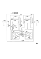
- FIG. 2 is a diagram showing an example of a functional configuration of a power supply device of the present invention.
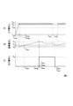
- FIG. 3 is a diagram for explaining the operation of the power supply device of the present invention.
- FIG. 2 shows an example of the functional configuration of the power supply device of the present invention.
- FIG. 3 is a diagram for explaining the operation of the power supply device of the present invention.
- the power supply device 200 of the present invention includes an input capacitor 210, a step-down DC/DC converter 230, a step-down control section 220, a power storage capacitor 240, a step-up DC/DC converter 290, and a step-up control section 280.
- Input capacitor 210 stores charge input from power source 910 .
- the power source 910 is, for example, a power source for energy harvesting such as a vibration power generation element, a piezoelectric element, or a solar cell, and supplies minute power.
- the potential at one end of the input capacitor is the input potential V cin , and the other end may be grounded directly or via a resistor.
- a capacitor with a small capacitance may be used so that the input potential V cin becomes high even with a small amount of charge.
- the input capacitor 210 may be a ceramic capacitor with a capacitance of approximately several tens of ⁇ F.
- the capacitance may be selected so that the maximum value of the input potential V cin is 12V, or the capacitance may be selected so that the maximum value is 35V.
- the step-down DC/DC converter 230 steps down the input potential V cin .
- step-down DC/DC converter 230 steps down the potential to 3.3V or less and stores the charge in power storage capacitor 240.
- Step-down DC/DC converter 230 may operate using the charge stored in input capacitor 210.
- components within power supply rail 310 operate using the charge stored in input capacitor 210.
- “Operating using the charge accumulated in the input capacitor 210” means that when the input potential V cin is higher than the potential V cinE necessary to operate the step-down DC/DC converter 230, the step-down control section 220, etc. , meaning that it operates with the power supplied from the input capacitor 210.
- the step-down control unit 220 causes the step-down DC/DC converter 230 to start stepping down the input potential when the input potential V cin satisfies a predetermined first input criterion, and when the input potential does not meet a predetermined second input criterion. Sometimes, the step-down DC/DC converter is made to stop stepping down the input potential.
- the input potential for satisfying the first input criterion (first reference potential V inH ) is higher than the input potential for satisfying the second input criterion (second reference potential V inL ).
- the step-down control section 220 may operate using the charge accumulated in the input capacitor. Since the input capacitor 210 has a small capacitance, it is easy to increase the input potential V cin . Therefore, the potential V cinE required to operate the step-down DC/DC converter 230, the step-down control section 220, etc. can be made sufficiently lower than the input potential (second reference potential V inL ) for satisfying the second input criterion.
- Power storage capacitor 240 has a larger capacity than input capacitor 210 and stores the charge output by step-down DC/DC converter 230.
- step-down DC/DC converter 230 moves charge from input capacitor 210 to power storage capacitor 240 while stepping down the potential.
- the potential at one end of the power storage capacitor 240 is the storage potential Vc , and the other end may be grounded directly or via a resistor.
- the capacitance of the power storage capacitor 240 may be set, for example, so that the maximum value of the storage potential Vc is 3.3V or 5V.
- a capacitor characterized by large capacity such as an electric double layer capacitor (EDLC) or a lithium ion capacitor, may be used.
- Capacitors with large capacity, such as electric double layer capacitors are more resistant to repeated charging and discharging and to low-temperature environments than secondary batteries, making them suitable for use in high-altitude regions and cold regions.
- the step-down control section 220 includes a hysteresis comparator 221, a DC power supply 222, and a step-down control switch 223.
- the potential V in supplied by the DC power supply 222 may also be generated using the charge accumulated in the input capacitor 210 (it may be generated using the input potential V cin ).
- the hysteresis comparator 221 sets a first reference potential V inH and a second reference potential V inL based on the potential V in .
- the step-down control switch 223 enters a connected state (a state in which the step-down DC/DC converter 230 steps down the input potential V cin ). Then, when the input potential V cin becomes less than the second reference potential V inL , the step-down control switch 223 is set to the cut-off state (the state in which the step-down DC/DC converter 230 stops stepping down the input potential V cin ).
- the step-down control switch 223 may be set to be in the connected state when the output of the hysteresis comparator 221 is in the High state, and the step-down control switch 223 may be in the disconnected state when the output of the hysteresis comparator 221 is in the Low state.
- the step-up DC/DC converter 290 boosts the voltage from the storage potential V c , which is the potential at one end of the power storage capacitor 240, to a predetermined output potential V out and outputs power.
- the step-up DC/DC converter 290 has a function of outputting 3.3V when the accumulated potential V c is 1.0 to 3.3V, or 5.0V when the accumulated potential V c is 2.0 to 5.0V. It has the function of outputting. In this way, step-up DC/DC converter 290 supplies power to load 920 at a predetermined potential (potential range).
- Boost DC/DC converter 290 operates using the charge stored in power storage capacitor 240. Note that in the configuration of FIG.
- components within power supply rail 320 operate using the charge stored in power storage capacitor 240.
- the components within the power supply rail 320 are configured to be able to operate at a potential VcE lower than a stop reference potential VL , which will be described later.
- “Operating using the charge stored in the power storage capacitor 240” means that when the stored potential Vc is higher than the potential VcE necessary to operate the component, the power storage capacitor 240 supplies the charge. This means that it runs on electricity.
- the boost control unit 280 causes the boost DC/DC converter 290 to start boosting when the accumulated potential Vc satisfies a predetermined starting criterion, and causes the boost DC/DC converter 290 to start boosting when the accumulated potential Vc does not meet a predetermined maintenance criterion. 290 to stop boosting the pressure.
- the accumulated potential for satisfying the starting criterion (starting reference potential V H ) is higher than the accumulated potential for satisfying the maintaining criterion (in other words, the stopping reference potential V L which is the reference potential for stopping when the maintaining criterion is not satisfied). expensive.
- the step-up DC/DC converter 290 has a function of outputting 3.3V when the accumulated potential Vc is 1.0 to 3.3V
- the start reference potential VH is set to 3.3V
- the stop reference potential VL may be set to 1.0V.
- the boost control section 280 includes a boost control switch 283, a start control section 250, a stop control section 260, and an OR circuit 270.
- Boost control switch 283 is arranged between one end of power storage capacitor 240 , which is storage potential V c , and boost DC/DC converter 290 .
- the activation control unit 250 connects the boost control switch 283 when the accumulated potential V c satisfies a predetermined activation criterion.
- the stop control unit 260 turns off the boost control switch 283 when the accumulated potential V c does not satisfy a predetermined maintenance criterion.
- Boost control switch 283 operates using the charge stored in power storage capacitor 240.
- the start control section 250 may operate using the charge accumulated in the input capacitor 210, and the stop control section 260 may operate using the output potential V out .
- the stop control unit 260 which is a component within the power supply rail 330, operates using the output potential V out (operates with the power supplied from the step-up DC/DC converter 290).
- the activation control section 250 includes a comparator 251 and a DC power supply 252.
- the potential V H supplied by the DC power supply 252 may also be generated using the charge accumulated in the input capacitor 210 (it may be generated using the input potential V cin ).
- the comparator 251 controls the boost control switch 283 to be in the connected state (the state in which the boost DC/DC converter 290 boosts the accumulated potential V c ) when the accumulated potential V c becomes equal to or higher than the activation reference potential V H .
- the boost control switch 283 may be in the connected state when the output of the comparator 251 is in the High state.
- the activation control unit 250 enters a predetermined state (for example, High state).
- the stop control section 260 includes a comparator 261 and a DC power supply 262.
- the potential V L supplied by the DC power supply 262 may be generated using the output potential V out .
- the comparator 261 controls the boost control switch 283 to be in a disconnected state (a state in which the boost DC/DC converter 290 stops boosting the accumulated potential V c ) when the accumulated potential V c becomes less than the stop reference potential V L do.
- the boost control switch 283 may be turned off when the output of the comparator 261 is in the Low state (when the maintenance criterion is not satisfied).
- the stop control section 260 when the output potential V out of the step-up DC/DC converter is a potential that allows the stop control section 260 to operate, and the accumulated potential V c satisfies a predetermined maintenance criterion, the stop control section 260 , it is sufficient to output the same state as the above-mentioned predetermined state (for example, High state).
- Boost control switch 283 is arranged between one end of power storage capacitor 240, which is the storage potential Vc , and boost DC/DC converter 290.
- the OR circuit 270 has two diodes 271 and 272, and connects the boost control switch 283 when the output of the start control section 250 or the output of the stop control section 260 is in the above-mentioned predetermined state (for example, High state). Make it.
- the boost control unit 280 of the present invention it is possible to increase the difference between the starting reference potential V H that causes the boost DC/DC converter 290 to start boosting the voltage and the stop reference potential V L that causes the boost DC/DC converter 290 to stop boosting. . Therefore, in the method of storing power in a capacitor, the width of hysteresis can be widened.
- the vertical axis of (A) shows the input potential V cin
- the vertical axis of (B) shows the accumulated potential V c
- the vertical axis of (C) shows the output potential V O.
- the step-down control unit 220 causes the step-down DC/DC converter 230 to start stepping down the input potential, and the charge is transferred from the input capacitor 210 to power storage. Move to capacitor 240. Therefore, the input potential V cin decreases and the storage potential V c increases.
- the step-down control section 220 causes the step-down DC/DC converter 230 to stop stepping down the input potential. Therefore, the transfer of charge from input capacitor 210 to power storage capacitor 240 is stopped. Therefore, the input potential V cin increases and the storage potential V c remains constant. As this process is repeated, charge is gradually accumulated in the power storage capacitor 240.
- the output from the activation control section 250 becomes High.
- V O V out
- the stop control unit 260 becomes operational (time T 330-on ), and the output from the stop control unit 260 becomes High (time T 260-high ).
- both the diode 271 side and the diode 272 side are in a High state, and the output from the OR circuit 270 is also in a High state.
- the accumulated electric potential V c decreases if more electric charge is outputted than the electric charge supplied from the power source 910.
- the output from the activation control section 250 becomes a Low state (time T 250-low ).
- the diode 271 side is in the Low state, but the diode 272 side is in the High state, so the output from the OR circuit 270 maintains the High state. Therefore, the output potential V O maintains V out .
- the accumulated potential V c varies depending on the supply of charge from the power source 910 and the level of the output charge.
- the accumulated potential V c gradually decreases.
- the output from the stop control unit 260 becomes a Low state (time T 260-low ), and both the diode 271 side and the diode 272 side become a Low state, so the OR circuit The output from 270 is also in a low state.
- the output potential V O from the step-up DC/DC converter 290 becomes 0V (time T 330-off ). Note that even if the supply of charge from the power source 910 does not stop, the same operation will occur if the accumulated potential Vc becomes lower than the stop reference potential VL due to large power consumption in the load 920. .
- a wide range is set between the storage potential (starting reference potential V H ) that satisfies the activation criteria for starting voltage boosting and the storage potential (stopping reference potential V L ) that satisfies the maintenance criteria for maintaining voltage boosting.
- the width of hysteresis can be widened, making it easier to stably supply power.
- the system since the system stores power in a capacitor, it is more resistant to repeated charging and discharging and to low-temperature environments than systems that use secondary batteries, making it suitable for use in high-altitude areas and cold regions.
- the start control section 250 By operating the start control section 250 using the charge accumulated in the input capacitor 210 and operating the stop control section 260 at the output potential, it is possible to operate as described using FIG. 3. At this time, if the stored potential V c is within the range of input potentials at which the step-up DC/DC converter 290 can output a predetermined potential, the output potential V out can be output. That is, it is also possible to set the start reference potential V H and the stop reference potential V L to the highest and lowest values of the allowable range of the input potential to the step-up DC/DC converter 290. Therefore, it is easier to set the hysteresis width wider.
Landscapes
- Engineering & Computer Science (AREA)
- Power Engineering (AREA)
- Charge And Discharge Circuits For Batteries Or The Like (AREA)
- Dc-Dc Converters (AREA)
- Stand-By Power Supply Arrangements (AREA)
Abstract
電源装置は、入力キャパシタ、降圧DC/DCコンバータ、降圧制御部、電力蓄積キャパシタ、昇圧DC/DCコンバータ、昇圧制御部を備える。降圧DC/DCコンバータは、入力キャパシタの入力電位を降圧させる。降圧制御部は、第1入力基準を満たすときに降圧を開始させ、第2入力基準を満たさないときに降圧を停止させる。電力蓄積キャパシタは、大容量であり、降圧DC/DCコンバータが出力する電荷を蓄積する。昇圧DC/DCコンバータは、蓄積電位から出力電位まで昇圧して電力を出力する。昇圧制御部は、起動基準を満たすときに昇圧を開始させ、維持基準を満たさないときに昇圧を停止させる。起動基準を満たす蓄積電位は、維持基準を満たす蓄積電位よりも高い。
Description
本発明は、微小電力を供給する電力源からの電力を入力とし、負荷回路に電力を供給するための電源装置に関する。
自然エネルギを利用した電力源からの電力を入力とし、負荷回路に電力を供給するための電源装置としては、二次電池に電力を蓄える方式とキャパシタに電力を蓄える方式がある。キャパシタに電力を蓄える方式は、二次電池に電力を蓄える方式よりも標高の高い地域または寒冷地での使用を想定した環境発電に適している。キャパシタに電力を蓄える方式では、特許文献1などが知られている。特許文献1の図1を、図1に示す。特許文献1の要約には、課題として『自然エネルギを利用して発電した微弱な電力で過大な負荷を駆動できる電源装置を提供する。』と示され、解決手段として『電源装置は、太陽電池等の自然エネルギを利用して発電する発電素子GEを含む電源10の出力端子T1と接続されて、端子T2に電源10から供給される電力を充電する容量SCと、充電電力の放電を制御する電力制御回路12と、所定の電圧を出力するレギュレータ13とを備え、容量に充電された電力で負荷14を駆動する。』と示されている。
しかしながら、特許文献1では電力供給のヒステリシス機構を、コンパレータおよび基準電圧源を用いて制御し、実現している。二次電池やバックアップ電池に頼らずキャパシタのみから電力を供給する場合、負荷への放電が進むにつれてキャパシタの電圧が下がるため、電力供給停止を判断する制御回路の動作電圧を確保できなくなるため、停止閾値電圧を制御回路の最低動作電圧以下に下げることができなかった。したがって、ヒステリシスの幅(負荷に電力を供給できるキャパシタの電圧の幅)を大きくとることが困難であった。
本発明は、キャパシタに電力を蓄える方式において、ヒステリシスの幅を広くすることを目的とする。
本発明の電源装置は、入力キャパシタ、降圧DC/DCコンバータ、降圧制御部、電力蓄積キャパシタ、昇圧DC/DCコンバータ、昇圧制御部を備える。入力キャパシタは、入力された電荷を蓄積する。降圧DC/DCコンバータは、入力キャパシタの一端の電位である入力電位を降圧させる。降圧制御部は、入力電位があらかじめ定めた第1入力基準を満たすときに降圧DC/DCコンバータに入力電位の降圧を開始させ、入力電位があらかじめ定めた第2入力基準を満たさないときに降圧DC/DCコンバータに入力電位の降圧を停止させる。第1入力基準を満たすための入力電位は、第2入力基準を満たすための入力電位よりも高い。電力蓄積キャパシタは、入力キャパシタよりも大容量であり、降圧DC/DCコンバータが出力する電荷を蓄積する。昇圧DC/DCコンバータは、電力蓄積キャパシタの一端の電位である蓄積電位から、あらかじめ定めた出力電位まで昇圧して電力を出力する。昇圧制御部は、蓄積電位があらかじめ定めた起動基準を満たすときに昇圧DC/DCコンバータに昇圧を開始させ、蓄積電位があらかじめ定めた維持基準を満たさないときに昇圧DC/DCコンバータに昇圧を停止させる。起動基準を満たすための蓄積電位は、維持基準を満たすための蓄積電位よりも高い。
本発明の電源装置によれば、昇圧を開始させる起動基準を満たす蓄電電位と、昇圧を維持させる維持基準を満たす蓄電電位との幅を広く設定しやすい。したがって、キャパシタに電力を蓄える方式において、ヒステリシスの幅を広くすることができる。
以下、本発明の実施の形態について、詳細に説明する。なお、同じ機能を有する構成部には同じ番号を付し、重複説明を省略する。
図2に本発明の電源装置に機能構成例を示す。図3は、本発明の電源装置の動作を説明するための図である。本発明の電源装置200は、入力キャパシタ210、降圧DC/DCコンバータ230、降圧制御部220、電力蓄積キャパシタ240、昇圧DC/DCコンバータ290、昇圧制御部280を備える。
入力キャパシタ210は、電力源910から入力された電荷を蓄積する。電力源910とは、例えば、振動発電素子、圧電素子、太陽電池などの環境発電用の電源であり、微小電力を供給する。入力キャパシタの一端の電位は入力電位Vcinであり、他端は直接もしくは抵抗などを介して接地すればよい。入力キャパシタ210は、少ない電荷でも入力電位Vcinが高くなるように小さい容量のコンデンサを用いればよい。例えば、入力キャパシタ210には、容量が数10μF程度のセラミックコンデンサを利用すればよい。例えば、入力電位Vcinの最大値が12Vとなるように容量を選択してもよいし、最大値が35Vとなるように容量を選択してもよい。
降圧DC/DCコンバータ230は、入力電位Vcinを降圧させる。例えば、降圧DC/DCコンバータ230は、電位を3.3V以下まで降圧し、電荷を電力蓄積キャパシタ240に蓄積する。降圧DC/DCコンバータ230は、入力キャパシタ210に蓄積された電荷を用いて動作すればよい。なお、図2の構成では、電源レール310内の構成部は、入力キャパシタ210に蓄積された電荷を用いて動作する。「入力キャパシタ210に蓄積された電荷を用いて動作する」とは、入力電位Vcinが降圧DC/DCコンバータ230、降圧制御部220などを動作させるために必要な電位VcinEよりも高いときに、入力キャパシタ210から供給される電力で動作することを意味している。
降圧制御部220は、入力電位Vcinがあらかじめ定めた第1入力基準を満たすときに降圧DC/DCコンバータ230に入力電位の降圧を開始させ、入力電位があらかじめ定めた第2入力基準を満たさないときに降圧DC/DCコンバータに入力電位の降圧を停止させる。第1入力基準を満たすための入力電位(第1基準電位VinH)は、第2入力基準を満たすための入力電位(第2基準電位VinL)よりも高い。降圧制御部220は、入力キャパシタに蓄積された電荷を用いて動作すればよい。入力キャパシタ210は容量が小さいため入力電位Vcinを高くしやすい。よって、降圧DC/DCコンバータ230、降圧制御部220などを動作させるために必要な電位VcinEは、第2入力基準を満たすための入力電位(第2基準電位VinL)よりも十分低くできる。
電力蓄積キャパシタ240は、入力キャパシタ210よりも大容量であり、降圧DC/DCコンバータ230が出力する電荷を蓄積する。言い換えると、降圧DC/DCコンバータ230は、電位を降圧させながら、電荷を入力キャパシタ210から電力蓄積キャパシタ240に移動させる。電力蓄積キャパシタ240の一端の電位は蓄積電位Vcであり、他端は直接もしくは抵抗などを介して接地すればよい。電力蓄積キャパシタ240の容量は、例えば、蓄積電位Vcの最大値が3.3Vもしくは5Vとなるように設定すればよい。電力蓄積キャパシタ240には、電気二重層キャパシタ(EDLC:Electrical Double Layer Capacitor)、リチウムイオンキャパシタなどの大容量を特徴とするコンデンサを用いればよい。電気二重層キャパシタなどの大容量を特徴とするキャパシタは、二次電池と比べると充放電の繰り返しや低温環境に対して強いため、標高の高い地域、寒冷地などでの使用に適している。
図2では、降圧制御部220は、ヒステリシスコンパレータ221、直流電源222、降圧制御スイッチ223を有する。直流電源222が供給する電位Vinも、入力キャパシタ210に蓄積された電荷を用いて生成すればよい(入力電位Vcinを用いて生成すればよい)。ヒステリシスコンパレータ221は電位Vinに基づいて第1基準電位VinHと第2基準電位VinLを設定する。そして、ヒステリシスコンパレータ221は、入力電位Vcinが第1基準電位VinH以上になったときに降圧制御スイッチ223が接続状態(降圧DC/DCコンバータ230が入力電位Vcinを降圧させる状態)となるよう制御し、その後、入力電位Vcinが第2基準電位VinL未満になったときに降圧制御スイッチ223が切断状態(降圧DC/DCコンバータ230が入力電位Vcinの降圧を停止する状態)となるよう制御する。例えば、ヒステリシスコンパレータ221の出力がHigh状態のときに降圧制御スイッチ223が接続状態、ヒステリシスコンパレータ221の出力がLow状態のときに降圧制御スイッチ223が切断状態となるように設定すればよい。
昇圧DC/DCコンバータ290は、電力蓄積キャパシタ240の一端の電位である蓄積電位Vcから、あらかじめ定めた出力電位Voutまで昇圧して電力を出力する。例えば、昇圧DC/DCコンバータ290は、蓄積電位Vcが1.0~3.3Vのときに3.3Vを出力するような機能、もしくは、2.0~5.0Vのときに5.0Vを出力するような機能を有する。このように、昇圧DC/DCコンバータ290は、あらかじめ定めた電位(電位の範囲)で電力を負荷920に供給する。昇圧DC/DCコンバータ290は、電力蓄積キャパシタ240に蓄積された電荷を用いて動作する。なお、図2の構成では、電源レール320内の構成部は、電力蓄積キャパシタ240に蓄積された電荷を用いて動作する。なお、電源レール320内の構成部は、後述する停止基準電位VLよりも低い電位VcEで動作できるようにしておく。「電力蓄積キャパシタ240に蓄積された電荷を用いて動作する」とは、蓄積電位Vcが構成部を動作させるために必要な電位VcEよりも高いときに、電力蓄積キャパシタ240ら供給される電力で動作することを意味している。
昇圧制御部280は、蓄積電位Vcがあらかじめ定めた起動基準を満たすときに昇圧DC/DCコンバータ290に昇圧を開始させ、蓄積電位があらかじめ定めた維持基準を満たさないときに昇圧DC/DCコンバータ290に昇圧を停止させる。起動基準を満たすための蓄積電位(起動基準電位VH)は、維持基準を満たすための蓄積電位(言い換えると、維持基準を満たさないときに停止させる基準電位である停止基準電位VL)よりも高い。例えば、昇圧DC/DCコンバータ290が、蓄積電位Vcが1.0~3.3Vのときに3.3Vを出力する機能を有する場合、起動基準電位VHを3.3Vとし、停止基準電位VLを1.0Vのように設定すればよい。
昇圧制御部280は、昇圧制御スイッチ283、起動制御部250、停止制御部260、OR回路270を有する。昇圧制御スイッチ283は、蓄積電位Vcである電力蓄積キャパシタ240の一端と、昇圧DC/DCコンバータ290との間に配置される。起動制御部250は、蓄積電位Vcがあらかじめ定めた起動基準を満たすときに昇圧制御スイッチ283を接続状態にする。停止制御部260は、蓄積電位Vcがあらかじめ定めた維持基準を満たさないときに昇圧制御スイッチ283を切断状態にする。昇圧制御スイッチ283は、電力蓄積キャパシタ240に蓄積された電荷を用いて動作する。起動制御部250は、入力キャパシタ210に蓄積された電荷を用いて動作し、停止制御部260は、出力電位Voutを用いて動作すればよい。図2の構成では、電源レール330内の構成部である停止制御部260は、出力電位Voutを用いて動作する(昇圧DC/DCコンバータ290から供給される電力で動作する)。
起動制御部250は、コンパレータ251と直流電源252を有する。直流電源252が供給する電位VHも、入力キャパシタ210に蓄積された電荷を用いて生成すればよい(入力電位Vcinを用いて生成すればよい)。コンパレータ251は、蓄積電位Vcが起動基準電位VH以上になったときに昇圧制御スイッチ283が接続状態(昇圧DC/DCコンバータ290が蓄積電位Vcを昇圧させる状態)となるよう制御する。例えば、コンパレータ251の出力がHigh状態のときに昇圧制御スイッチ283が接続状態となるようにすればよい。言い換えると、起動制御部250は、入力電位Vcinが起動制御部250を動作させることができる電位であり、かつ、蓄積電位Vcがあらかじめ定めた起動基準を満たすときに、所定状態(例えば、High状態)を出力すればよい。
停止制御部260は、コンパレータ261と直流電源262を有する。直流電源262が供給する電位VLは、出力電位Voutを用いて生成すればよい。コンパレータ261は、蓄積電位Vcが停止基準電位VL未満になったときに昇圧制御スイッチ283が切断状態(昇圧DC/DCコンバータ290が蓄積電位Vcの昇圧を停止する状態)となるよう制御する。例えば、コンパレータ261の出力がLow状態のとき(維持基準を満たさないとき)に昇圧制御スイッチ283が切断状態となるようにすればよい。言い換えると、停止制御部260は、昇圧DC/DCコンバータの出力電位Voutが停止制御部260を動作させることができる電位であり、かつ、蓄積電位Vcがあらかじめ定めた維持基準を満たすときに、上述の所定状態(例えば、High状態)と同じ状態を出力すればよい。
昇圧制御スイッチ283は、蓄積電位Vcである電力蓄積キャパシタ240の一端と、昇圧DC/DCコンバータ290との間に配置されている。OR回路270は、2つのダイオード271,272を有し、起動制御部250の出力または停止制御部260の出力が上述の所定状態(例えば、High状態)のときに、昇圧制御スイッチ283を接続状態にする。
本発明の昇圧制御部280によれば、昇圧DC/DCコンバータ290に昇圧を開始させる起動基準電位VHと昇圧DC/DCコンバータ290の昇圧を停止させる停止基準電位VLとの差を大きくできる。したがって、キャパシタに電力を蓄える方式において、ヒステリシスの幅を広くすることができる。
次に、図3を用いて、電源装置の動作を説明する。(A)の縦軸は入力電位Vcinを、(B)の縦軸は蓄積電位Vcを、(C)の縦軸は出力電位VOを示している。いずれの図も横軸は時間である。初期状態として入力キャパシタ210にも電力蓄積キャパシタ240にも電荷は蓄えられていないとする。つまり、入力電位Vcin=0、蓄積電位Vc=0、出力電位VO=0である。時刻Tin-on1から電力源910が電荷を供給し始めたとする。入力電位Vcinは次第に上昇し、電源レール310内の構成部を動作させることができる電位VcinEを超えると、降圧DC/DCコンバータ230、降圧制御部220、起動制御部250が動作できる状態になる。
時刻T221-highに、入力電位Vcinが第1基準電位VinHに達すると、降圧制御部220が降圧DC/DCコンバータ230に入力電位の降圧を開始させ、電荷が入力キャパシタ210から電力蓄積キャパシタ240に移動する。よって、入力電位Vcinは低下し、蓄積電位Vcは上昇する。時刻T221-lowに、入力電位Vcinが第2基準電位VinLに達すると、降圧制御部220が降圧DC/DCコンバータ230に入力電位の降圧を停止させる。したがって、入力キャパシタ210から電力蓄積キャパシタ240への電荷の移動は止まる。よって、入力電位Vcinは上昇し、蓄積電位Vcは一定となる。この処理を繰り返しながら、電力蓄積キャパシタ240には次第に電荷が蓄積される。
時刻T320-onに、蓄積電位Vcが電位VcEに達すると、昇圧DC/DCコンバータ290と昇圧制御スイッチ283が動作できる状態になる。その後も、電力源910が電荷を供給し続ければ、電力蓄積キャパシタ240には次第に電荷が蓄積される。
時刻T250-highに、蓄積電位Vcが起動基準電位VHに達すると、起動制御部250からの出力がHigh状態となる。図2の例では、ダイオード271側がHigh状態なので、OR回路270からの出力もHigh状態となる。そして、昇圧制御スイッチ283が接続状態となるので、昇圧DC/DCコンバータ290が、蓄積電位Vcをあらかじめ定めた出力電位Voutまで昇圧して電力を出力する(VO=Vout)。蓄積電位Vcが起動基準電位VHに達してから出力電位Voutが提供されるまでには、一般的には、少しだが時間の差がある。よって、時刻T250-highから少し遅れて、停止制御部260が動作可能になり(時刻T330-on)、停止制御部260からの出力がHigh状態となる(時刻T260-high)。このときは、ダイオード271側もダイオード272側もHigh状態であり、OR回路270からの出力もHigh状態である。
電力蓄積キャパシタ240の電荷を用いて負荷920に電力を供給するので、電力源910からの電荷の供給よりも、出力する電荷が多いと蓄積電位Vcは下がる。蓄積電位Vcが起動基準電位VHよりも低くなると、起動制御部250からの出力がLow状態となる(時刻T250-low)。このときは、ダイオード271側はLow状態になるが、ダイオード272側がHigh状態なので、OR回路270からの出力はHigh状態を維持する。したがって、出力電位VOはVoutを維持する。その後は、電力源910からの電荷の供給と出力する電荷の程度によって、蓄積電位Vcは変動する。
例えば、図3に示すように、時刻Tin-offに電力源910からの電荷の供給が止まった場合、次第に蓄積電位Vcは下がる。蓄積電位Vcが停止基準電位VLよりも低くなると、停止制御部260からの出力がLow状態となり(時刻T260-low)、ダイオード271側もダイオード272側もLow状態となるので、OR回路270からの出力もLow状態となる。そして、昇圧DC/DCコンバータ290からの出力電位VOは、0Vとなる(時刻T330-off)。なお、電力源910からの電荷の供給が止まらなくても、負荷920での電力消費が大きいことが原因で蓄積電位Vcが停止基準電位VLよりも低くなった場合も、同様に動作する。
再び、時刻Tin-on2から、電力源910が電荷を供給し始めると、電力蓄積キャパシタ240への電荷の蓄積が始まり、蓄積電位Vcが上昇する。
電源装置200によれば、昇圧を開始させる起動基準を満たす蓄電電位(起動基準電位VH)と、昇圧を維持させる維持基準を満たす蓄電電位(停止基準電位VL)との幅を広く設定しやすい。したがって、キャパシタに電力を蓄える方式において、ヒステリシスの幅を広くすることができ、安定的に電力を供給しやすい。また、キャパシタに電力を蓄える方式なので、二次電池を用いる方式と比べると充放電の繰り返しや低温環境に対して強いため、標高の高い地域、寒冷地などでの使用に適している。
起動制御部250を入力キャパシタ210に蓄積された電荷を用いて動作させ、停止制御部260を出力電位で動作させることで、図3を用いて説明したように動作させることができる。このときは、昇圧DC/DCコンバータ290があらかじめ定めた電位を出力できる入力電位の範囲に蓄電電位Vcがあれば、出力電位Voutを出力できる。つまり、起動基準電位VHと停止基準電位VLを、昇圧DC/DCコンバータ290への入力電位の許容範囲の最高値と最低値に設定することも可能である。よって、さらにヒステリシスの幅を広く設定しやすい。
200 電源装置 210 入力キャパシタ
220 降圧制御部 221 ヒステリシスコンパレータ
222,252,262 直流電源 223 降圧制御スイッチ
230 降圧DC/DCコンバータ 240 電力蓄積キャパシタ
250 起動制御部 251,261 コンパレータ
260 停止制御部 270 OR回路
271,272 ダイオード 280 昇圧制御部
283 昇圧制御スイッチ 290 昇圧DC/DCコンバータ
310,320,330 電源レール 910 電力源
920 負荷
220 降圧制御部 221 ヒステリシスコンパレータ
222,252,262 直流電源 223 降圧制御スイッチ
230 降圧DC/DCコンバータ 240 電力蓄積キャパシタ
250 起動制御部 251,261 コンパレータ
260 停止制御部 270 OR回路
271,272 ダイオード 280 昇圧制御部
283 昇圧制御スイッチ 290 昇圧DC/DCコンバータ
310,320,330 電源レール 910 電力源
920 負荷
Claims (6)
- 入力された電荷を蓄積する入力キャパシタと、
前記入力キャパシタの一端の電位である入力電位を降圧させる降圧DC/DCコンバータと、
前記入力電位があらかじめ定めた第1入力基準を満たすときに前記降圧DC/DCコンバータに前記入力電位の降圧を開始させ、前記入力電位があらかじめ定めた第2入力基準を満たさないときに前記降圧DC/DCコンバータに前記入力電位の降圧を停止させる降圧制御部と、
前記入力キャパシタよりも大容量であり、前記降圧DC/DCコンバータが出力する電荷を蓄積する電力蓄積キャパシタと、
前記電力蓄積キャパシタの一端の電位である蓄積電位から、あらかじめ定めた出力電位まで昇圧して電力を出力する昇圧DC/DCコンバータと、
前記蓄積電位があらかじめ定めた起動基準を満たすときに前記昇圧DC/DCコンバータに昇圧を開始させ、前記蓄積電位があらかじめ定めた維持基準を満たさないときに前記昇圧DC/DCコンバータに昇圧を停止させる昇圧制御部と、
を備え、
前記第1入力基準を満たすための入力電位は、前記第2入力基準を満たすための入力電位よりも高く、
前記起動基準を満たすための蓄積電位は、前記維持基準を満たすための蓄積電位よりも高い
ことを特徴とする電源装置。 - 請求項1記載の電源装置であって、
前記昇圧制御部は、
前記蓄積電位である前記電力蓄積キャパシタの一端と、前記昇圧DC/DCコンバータとの間に配置された昇圧制御スイッチと、
前記蓄積電位があらかじめ定めた起動基準を満たすときに前記昇圧制御スイッチを接続状態にする起動制御部と、
前記蓄積電位があらかじめ定めた維持基準を満たさないときに前記昇圧制御スイッチを切断状態にする停止制御部と、
を有することを特徴とする電源装置。 - 請求項2記載の電源装置であって、
前記起動制御部は、前記入力キャパシタに蓄積された電荷を用いて動作し、
前記停止制御部は、前記出力電位を用いて動作する
ことを特徴とする電源装置。 - 請求項1記載の電源装置であって、
前記昇圧制御部は、昇圧制御スイッチと起動制御部と停止制御部を有し、
前記起動制御部は、前記入力キャパシタに蓄積された電荷を用いて動作し、
前記停止制御部は、前記出力電位を用いて動作し、
前記起動制御部は、前記入力電位が当該起動制御部を動作させることができる電位であり、かつ、前記蓄積電位があらかじめ定めた起動基準を満たすときに、所定状態の出力をし、
前記停止制御部は、前記昇圧DC/DCコンバータの出力が当該停止制御部を動作させることができる電位であり、かつ、前記蓄積電位があらかじめ定めた維持基準を満たすときに、前記所定状態と同じ状態の出力をし、
前記昇圧制御スイッチは、前記蓄積電位である前記電力蓄積キャパシタの一端と、前記昇圧DC/DCコンバータとの間に配置されており、前記起動制御部の出力または前記停
止制御部の出力が前記所定状態のときに接続状態である
ことを特徴とする電源装置。 - 請求項3または4記載の電源装置であって、
前記降圧DC/DCコンバータ、前記降圧制御部は、前記入力キャパシタに蓄積された電荷を用いて動作する
ことを特徴とする電源装置。 - 請求項3または4記載の電源装置であって、
前記昇圧DC/DCコンバータ、前記昇圧制御スイッチは、前記電力蓄積キャパシタに蓄積された電荷を用いて動作する
ことを特徴とする電源装置。
Applications Claiming Priority (2)
| Application Number | Priority Date | Filing Date | Title |
|---|---|---|---|
| JP2022072470A JP7297972B1 (ja) | 2022-04-26 | 2022-04-26 | 電源装置 |
| JP2022-072470 | 2022-04-26 |
Publications (1)
| Publication Number | Publication Date |
|---|---|
| WO2023210256A1 true WO2023210256A1 (ja) | 2023-11-02 |
Family
ID=86900481
Family Applications (1)
| Application Number | Title | Priority Date | Filing Date |
|---|---|---|---|
| PCT/JP2023/013471 Ceased WO2023210256A1 (ja) | 2022-04-26 | 2023-03-31 | 電源装置 |
Country Status (2)
| Country | Link |
|---|---|
| JP (1) | JP7297972B1 (ja) |
| WO (1) | WO2023210256A1 (ja) |
Citations (3)
| Publication number | Priority date | Publication date | Assignee | Title |
|---|---|---|---|---|
| JP2014207767A (ja) * | 2013-04-12 | 2014-10-30 | パナソニック株式会社 | エネルギ変換装置 |
| JP6523592B1 (ja) * | 2018-12-18 | 2019-06-05 | 三菱電機株式会社 | 電力変換装置 |
| WO2020075371A1 (ja) * | 2018-10-10 | 2020-04-16 | パナソニックIpマネジメント株式会社 | 電源回路、起動回路、発電装置、及び電子機器 |
-
2022
- 2022-04-26 JP JP2022072470A patent/JP7297972B1/ja active Active
-
2023
- 2023-03-31 WO PCT/JP2023/013471 patent/WO2023210256A1/ja not_active Ceased
Patent Citations (3)
| Publication number | Priority date | Publication date | Assignee | Title |
|---|---|---|---|---|
| JP2014207767A (ja) * | 2013-04-12 | 2014-10-30 | パナソニック株式会社 | エネルギ変換装置 |
| WO2020075371A1 (ja) * | 2018-10-10 | 2020-04-16 | パナソニックIpマネジメント株式会社 | 電源回路、起動回路、発電装置、及び電子機器 |
| JP6523592B1 (ja) * | 2018-12-18 | 2019-06-05 | 三菱電機株式会社 | 電力変換装置 |
Also Published As
| Publication number | Publication date |
|---|---|
| JP7297972B1 (ja) | 2023-06-26 |
| JP2023161859A (ja) | 2023-11-08 |
Similar Documents
| Publication | Publication Date | Title |
|---|---|---|
| US5572108A (en) | Power system using battery-charged capacitors | |
| US9415732B2 (en) | Vehicle power unit | |
| US8035356B2 (en) | Ultra-capacitor based uninterruptible power supply | |
| US9150170B2 (en) | Circuit system for redistribution of electrical energy in a vehicle | |
| CN106464005B (zh) | 不间断电源装置 | |
| RU2418721C2 (ru) | Система электропитания для электроснабжения по меньшей мере одного потребителя на летательном аппарате | |
| US5642027A (en) | Current-limited system for capacitive load powering | |
| AU2010350279B2 (en) | Device and method for compensating for the power of an electric load of a vehicle using a high-capacity capacitor | |
| US8135965B2 (en) | Apparatus and method for distributed standby power provision | |
| JP2005500792A (ja) | 光電池の改良 | |
| US20150203060A1 (en) | Power supply management system and power supply management method | |
| CN106463989A (zh) | 引擎启动与电池支持模块 | |
| JP5182788B2 (ja) | 電力供給装置およびそれを用いた電力供給システム | |
| CN104426452A (zh) | 用于空气轴承电机的驱动电路 | |
| KR102186488B1 (ko) | 자동차 배터리 비상 충전 장치 및 방법 | |
| JP2016092958A (ja) | 電源回路装置 | |
| CN203456938U (zh) | 汽车电源失能的急救装置 | |
| CN111600371A (zh) | 一种太阳能超级电容电源自动控制方法及装置 | |
| WO2018189953A1 (ja) | 電力変換装置および非接触給電システム | |
| CN215300494U (zh) | 一种降压型dcdc变换器及其欠压保护电路 | |
| WO2018074144A1 (ja) | 電源回路 | |
| JP5073436B2 (ja) | 無瞬断バックアップ電源 | |
| EP3891860A1 (en) | Method and device for energy harvesting using a cold-start voltage converter | |
| JP2023161859A (ja) | 電源装置 | |
| JP2009296719A (ja) | 直流バックアップ電源システムおよびその充電方法 |
Legal Events
| Date | Code | Title | Description |
|---|---|---|---|
| 121 | Ep: the epo has been informed by wipo that ep was designated in this application |
Ref document number: 23796003 Country of ref document: EP Kind code of ref document: A1 |
|
| NENP | Non-entry into the national phase |
Ref country code: DE |
|
| 122 | Ep: pct application non-entry in european phase |
Ref document number: 23796003 Country of ref document: EP Kind code of ref document: A1 |