WO2023203425A1 - Semiconductor device and method for semiconductor device fabrication - Google Patents
Semiconductor device and method for semiconductor device fabrication Download PDFInfo
- Publication number
- WO2023203425A1 WO2023203425A1 PCT/IB2023/053563 IB2023053563W WO2023203425A1 WO 2023203425 A1 WO2023203425 A1 WO 2023203425A1 IB 2023053563 W IB2023053563 W IB 2023053563W WO 2023203425 A1 WO2023203425 A1 WO 2023203425A1
- Authority
- WO
- WIPO (PCT)
- Prior art keywords
- layer
- insulating layer
- conductive layer
- insulating
- film
- Prior art date
Links
- 239000004065 semiconductor Substances 0.000 title claims abstract description 373
- 238000000034 method Methods 0.000 title claims description 280
- 238000005389 semiconductor device fabrication Methods 0.000 title 1
- 230000006870 function Effects 0.000 claims description 153
- 238000004519 manufacturing process Methods 0.000 claims description 66
- 238000005530 etching Methods 0.000 claims description 40
- 238000012545 processing Methods 0.000 claims description 33
- 238000000206 photolithography Methods 0.000 claims description 17
- 239000010410 layer Substances 0.000 description 2373
- 239000010408 film Substances 0.000 description 458
- 239000000463 material Substances 0.000 description 160
- 239000011701 zinc Substances 0.000 description 145
- 239000000758 substrate Substances 0.000 description 130
- 239000001301 oxygen Substances 0.000 description 125
- 229910052760 oxygen Inorganic materials 0.000 description 125
- QVGXLLKOCUKJST-UHFFFAOYSA-N atomic oxygen Chemical compound [O] QVGXLLKOCUKJST-UHFFFAOYSA-N 0.000 description 123
- 229910044991 metal oxide Inorganic materials 0.000 description 123
- 150000004706 metal oxides Chemical class 0.000 description 123
- 238000005401 electroluminescence Methods 0.000 description 115
- 229910052751 metal Inorganic materials 0.000 description 65
- 239000002184 metal Substances 0.000 description 50
- GYHNNYVSQQEPJS-UHFFFAOYSA-N Gallium Chemical group [Ga] GYHNNYVSQQEPJS-UHFFFAOYSA-N 0.000 description 47
- 125000004429 atom Chemical group 0.000 description 47
- 229910052733 gallium Inorganic materials 0.000 description 47
- 230000008569 process Effects 0.000 description 44
- 238000000231 atomic layer deposition Methods 0.000 description 43
- 230000015572 biosynthetic process Effects 0.000 description 41
- 239000001257 hydrogen Substances 0.000 description 41
- 229910052739 hydrogen Inorganic materials 0.000 description 41
- APFVFJFRJDLVQX-UHFFFAOYSA-N indium atom Chemical compound [In] APFVFJFRJDLVQX-UHFFFAOYSA-N 0.000 description 41
- 229910052738 indium Inorganic materials 0.000 description 38
- 229920005989 resin Polymers 0.000 description 38
- 239000011347 resin Substances 0.000 description 38
- IJGRMHOSHXDMSA-UHFFFAOYSA-N Atomic nitrogen Chemical compound N#N IJGRMHOSHXDMSA-UHFFFAOYSA-N 0.000 description 37
- 239000000126 substance Substances 0.000 description 37
- UFHFLCQGNIYNRP-UHFFFAOYSA-N Hydrogen Chemical compound [H][H] UFHFLCQGNIYNRP-UHFFFAOYSA-N 0.000 description 36
- XUIMIQQOPSSXEZ-UHFFFAOYSA-N Silicon Chemical compound [Si] XUIMIQQOPSSXEZ-UHFFFAOYSA-N 0.000 description 36
- 239000000203 mixture Substances 0.000 description 36
- 239000011241 protective layer Substances 0.000 description 36
- 229910052710 silicon Inorganic materials 0.000 description 36
- 239000010703 silicon Substances 0.000 description 36
- 238000004544 sputter deposition Methods 0.000 description 34
- XLYOFNOQVPJJNP-UHFFFAOYSA-N water Substances O XLYOFNOQVPJJNP-UHFFFAOYSA-N 0.000 description 32
- HCHKCACWOHOZIP-UHFFFAOYSA-N Zinc Chemical compound [Zn] HCHKCACWOHOZIP-UHFFFAOYSA-N 0.000 description 30
- 150000004767 nitrides Chemical class 0.000 description 30
- TWNQGVIAIRXVLR-UHFFFAOYSA-N oxo(oxoalumanyloxy)alumane Chemical compound O=[Al]O[Al]=O TWNQGVIAIRXVLR-UHFFFAOYSA-N 0.000 description 30
- 229910052725 zinc Inorganic materials 0.000 description 30
- 229910052581 Si3N4 Inorganic materials 0.000 description 29
- HQVNEWCFYHHQES-UHFFFAOYSA-N silicon nitride Chemical compound N12[Si]34N5[Si]62N3[Si]51N64 HQVNEWCFYHHQES-UHFFFAOYSA-N 0.000 description 29
- 229910052782 aluminium Inorganic materials 0.000 description 28
- XAGFODPZIPBFFR-UHFFFAOYSA-N aluminium Chemical group [Al] XAGFODPZIPBFFR-UHFFFAOYSA-N 0.000 description 28
- 239000012535 impurity Substances 0.000 description 28
- 238000002347 injection Methods 0.000 description 28
- 239000007924 injection Substances 0.000 description 28
- 239000003990 capacitor Substances 0.000 description 27
- VYPSYNLAJGMNEJ-UHFFFAOYSA-N Silicium dioxide Chemical compound O=[Si]=O VYPSYNLAJGMNEJ-UHFFFAOYSA-N 0.000 description 25
- 239000011810 insulating material Substances 0.000 description 23
- 230000003287 optical effect Effects 0.000 description 22
- PXHVJJICTQNCMI-UHFFFAOYSA-N Nickel Chemical group [Ni] PXHVJJICTQNCMI-UHFFFAOYSA-N 0.000 description 21
- 230000000903 blocking effect Effects 0.000 description 21
- 238000010438 heat treatment Methods 0.000 description 21
- 229910052814 silicon oxide Inorganic materials 0.000 description 21
- 238000012360 testing method Methods 0.000 description 21
- 239000010409 thin film Substances 0.000 description 20
- XEEYBQQBJWHFJM-UHFFFAOYSA-N Iron Chemical group [Fe] XEEYBQQBJWHFJM-UHFFFAOYSA-N 0.000 description 19
- 239000000956 alloy Substances 0.000 description 19
- 229910045601 alloy Inorganic materials 0.000 description 18
- 238000004891 communication Methods 0.000 description 18
- 238000010586 diagram Methods 0.000 description 18
- 229910052757 nitrogen Inorganic materials 0.000 description 18
- 238000007740 vapor deposition Methods 0.000 description 18
- -1 element M Chemical compound 0.000 description 17
- 230000004888 barrier function Effects 0.000 description 16
- 238000005229 chemical vapour deposition Methods 0.000 description 16
- 239000003086 colorant Substances 0.000 description 16
- 239000004020 conductor Substances 0.000 description 16
- 239000007789 gas Substances 0.000 description 16
- 238000009792 diffusion process Methods 0.000 description 15
- 239000002243 precursor Substances 0.000 description 15
- 239000010936 titanium Chemical group 0.000 description 15
- 239000012298 atmosphere Substances 0.000 description 14
- 150000001875 compounds Chemical class 0.000 description 14
- 230000003647 oxidation Effects 0.000 description 14
- 238000007254 oxidation reaction Methods 0.000 description 14
- 230000006378 damage Effects 0.000 description 13
- 229910000449 hafnium oxide Inorganic materials 0.000 description 13
- WIHZLLGSGQNAGK-UHFFFAOYSA-N hafnium(4+);oxygen(2-) Chemical compound [O-2].[O-2].[Hf+4] WIHZLLGSGQNAGK-UHFFFAOYSA-N 0.000 description 13
- 150000002739 metals Chemical class 0.000 description 13
- WFKWXMTUELFFGS-UHFFFAOYSA-N tungsten Chemical group [W] WFKWXMTUELFFGS-UHFFFAOYSA-N 0.000 description 13
- 229910052721 tungsten Inorganic materials 0.000 description 13
- 239000010937 tungsten Chemical group 0.000 description 13
- RYGMFSIKBFXOCR-UHFFFAOYSA-N Copper Chemical group [Cu] RYGMFSIKBFXOCR-UHFFFAOYSA-N 0.000 description 12
- 239000010949 copper Chemical group 0.000 description 12
- 238000001039 wet etching Methods 0.000 description 12
- RTAQQCXQSZGOHL-UHFFFAOYSA-N Titanium Chemical group [Ti] RTAQQCXQSZGOHL-UHFFFAOYSA-N 0.000 description 11
- 238000006243 chemical reaction Methods 0.000 description 11
- 229910052802 copper Inorganic materials 0.000 description 11
- 238000001312 dry etching Methods 0.000 description 11
- 229910052750 molybdenum Inorganic materials 0.000 description 11
- 229910052759 nickel Inorganic materials 0.000 description 11
- 229910052715 tantalum Inorganic materials 0.000 description 11
- 229910052719 titanium Inorganic materials 0.000 description 11
- ZOKXTWBITQBERF-UHFFFAOYSA-N Molybdenum Chemical group [Mo] ZOKXTWBITQBERF-UHFFFAOYSA-N 0.000 description 10
- 230000007547 defect Effects 0.000 description 10
- 239000011521 glass Substances 0.000 description 10
- 229910052735 hafnium Inorganic materials 0.000 description 10
- 230000005525 hole transport Effects 0.000 description 10
- 238000003384 imaging method Methods 0.000 description 10
- 229910052742 iron Inorganic materials 0.000 description 10
- 239000011733 molybdenum Chemical group 0.000 description 10
- 230000005855 radiation Effects 0.000 description 10
- GUVRBAGPIYLISA-UHFFFAOYSA-N tantalum atom Chemical group [Ta] GUVRBAGPIYLISA-UHFFFAOYSA-N 0.000 description 10
- ATJFFYVFTNAWJD-UHFFFAOYSA-N Tin Chemical group [Sn] ATJFFYVFTNAWJD-UHFFFAOYSA-N 0.000 description 9
- 239000012790 adhesive layer Substances 0.000 description 9
- 229910052804 chromium Inorganic materials 0.000 description 9
- 239000011651 chromium Substances 0.000 description 9
- 238000000576 coating method Methods 0.000 description 9
- 239000011368 organic material Substances 0.000 description 9
- 238000005498 polishing Methods 0.000 description 9
- 229910052718 tin Inorganic materials 0.000 description 9
- 229910052727 yttrium Inorganic materials 0.000 description 9
- 239000004925 Acrylic resin Substances 0.000 description 8
- 229920000178 Acrylic resin Polymers 0.000 description 8
- VYZAMTAEIAYCRO-UHFFFAOYSA-N Chromium Chemical compound [Cr] VYZAMTAEIAYCRO-UHFFFAOYSA-N 0.000 description 8
- 229910001111 Fine metal Inorganic materials 0.000 description 8
- BQCADISMDOOEFD-UHFFFAOYSA-N Silver Chemical compound [Ag] BQCADISMDOOEFD-UHFFFAOYSA-N 0.000 description 8
- 239000000853 adhesive Substances 0.000 description 8
- 230000001070 adhesive effect Effects 0.000 description 8
- 230000008859 change Effects 0.000 description 8
- 229910017052 cobalt Inorganic materials 0.000 description 8
- 239000010941 cobalt Chemical group 0.000 description 8
- GUTLYIVDDKVIGB-UHFFFAOYSA-N cobalt atom Chemical group [Co] GUTLYIVDDKVIGB-UHFFFAOYSA-N 0.000 description 8
- VBJZVLUMGGDVMO-UHFFFAOYSA-N hafnium atom Chemical group [Hf] VBJZVLUMGGDVMO-UHFFFAOYSA-N 0.000 description 8
- 229910010272 inorganic material Inorganic materials 0.000 description 8
- 239000002346 layers by function Substances 0.000 description 8
- 150000002894 organic compounds Chemical class 0.000 description 8
- 238000009832 plasma treatment Methods 0.000 description 8
- 229920001721 polyimide Polymers 0.000 description 8
- 229910052709 silver Inorganic materials 0.000 description 8
- 239000004332 silver Substances 0.000 description 8
- 238000012546 transfer Methods 0.000 description 8
- 238000004458 analytical method Methods 0.000 description 7
- 229910052796 boron Inorganic materials 0.000 description 7
- 230000000694 effects Effects 0.000 description 7
- 230000005684 electric field Effects 0.000 description 7
- PCHJSUWPFVWCPO-UHFFFAOYSA-N gold Chemical compound [Au] PCHJSUWPFVWCPO-UHFFFAOYSA-N 0.000 description 7
- 229910052737 gold Inorganic materials 0.000 description 7
- 239000010931 gold Substances 0.000 description 7
- 230000007246 mechanism Effects 0.000 description 7
- 238000007639 printing Methods 0.000 description 7
- 239000002356 single layer Substances 0.000 description 7
- 238000001771 vacuum deposition Methods 0.000 description 7
- KDLHZDBZIXYQEI-UHFFFAOYSA-N Palladium Chemical compound [Pd] KDLHZDBZIXYQEI-UHFFFAOYSA-N 0.000 description 6
- 238000004833 X-ray photoelectron spectroscopy Methods 0.000 description 6
- XLOMVQKBTHCTTD-UHFFFAOYSA-N Zinc monoxide Chemical compound [Zn]=O XLOMVQKBTHCTTD-UHFFFAOYSA-N 0.000 description 6
- 238000001514 detection method Methods 0.000 description 6
- 230000006866 deterioration Effects 0.000 description 6
- 230000005669 field effect Effects 0.000 description 6
- 150000002431 hydrogen Chemical class 0.000 description 6
- 229910003437 indium oxide Inorganic materials 0.000 description 6
- PJXISJQVUVHSOJ-UHFFFAOYSA-N indium(iii) oxide Chemical compound [O-2].[O-2].[O-2].[In+3].[In+3] PJXISJQVUVHSOJ-UHFFFAOYSA-N 0.000 description 6
- AMGQUBHHOARCQH-UHFFFAOYSA-N indium;oxotin Chemical compound [In].[Sn]=O AMGQUBHHOARCQH-UHFFFAOYSA-N 0.000 description 6
- 239000004973 liquid crystal related substance Substances 0.000 description 6
- 239000011159 matrix material Substances 0.000 description 6
- 238000000623 plasma-assisted chemical vapour deposition Methods 0.000 description 6
- VWQVUPCCIRVNHF-UHFFFAOYSA-N yttrium atom Chemical group [Y] VWQVUPCCIRVNHF-UHFFFAOYSA-N 0.000 description 6
- 229910018137 Al-Zn Inorganic materials 0.000 description 5
- 229910018573 Al—Zn Inorganic materials 0.000 description 5
- FYYHWMGAXLPEAU-UHFFFAOYSA-N Magnesium Chemical group [Mg] FYYHWMGAXLPEAU-UHFFFAOYSA-N 0.000 description 5
- 239000004372 Polyvinyl alcohol Substances 0.000 description 5
- 229910020994 Sn-Zn Inorganic materials 0.000 description 5
- 229910009069 Sn—Zn Inorganic materials 0.000 description 5
- 229910021417 amorphous silicon Inorganic materials 0.000 description 5
- 238000000151 deposition Methods 0.000 description 5
- 230000008021 deposition Effects 0.000 description 5
- AJNVQOSZGJRYEI-UHFFFAOYSA-N digallium;oxygen(2-) Chemical compound [O-2].[O-2].[O-2].[Ga+3].[Ga+3] AJNVQOSZGJRYEI-UHFFFAOYSA-N 0.000 description 5
- 229910001195 gallium oxide Inorganic materials 0.000 description 5
- 210000003128 head Anatomy 0.000 description 5
- 239000011147 inorganic material Substances 0.000 description 5
- 239000011777 magnesium Chemical group 0.000 description 5
- WPBNNNQJVZRUHP-UHFFFAOYSA-L manganese(2+);methyl n-[[2-(methoxycarbonylcarbamothioylamino)phenyl]carbamothioyl]carbamate;n-[2-(sulfidocarbothioylamino)ethyl]carbamodithioate Chemical compound [Mn+2].[S-]C(=S)NCCNC([S-])=S.COC(=O)NC(=S)NC1=CC=CC=C1NC(=S)NC(=O)OC WPBNNNQJVZRUHP-UHFFFAOYSA-L 0.000 description 5
- 230000002093 peripheral effect Effects 0.000 description 5
- 229920006122 polyamide resin Polymers 0.000 description 5
- 229910021420 polycrystalline silicon Inorganic materials 0.000 description 5
- 239000009719 polyimide resin Substances 0.000 description 5
- 229920002451 polyvinyl alcohol Polymers 0.000 description 5
- 230000001681 protective effect Effects 0.000 description 5
- 239000002096 quantum dot Substances 0.000 description 5
- 239000002994 raw material Substances 0.000 description 5
- 239000002904 solvent Substances 0.000 description 5
- 238000002230 thermal chemical vapour deposition Methods 0.000 description 5
- OKTJSMMVPCPJKN-UHFFFAOYSA-N Carbon Chemical compound [C] OKTJSMMVPCPJKN-UHFFFAOYSA-N 0.000 description 4
- KRHYYFGTRYWZRS-UHFFFAOYSA-N Fluorane Chemical compound F KRHYYFGTRYWZRS-UHFFFAOYSA-N 0.000 description 4
- NBIIXXVUZAFLBC-UHFFFAOYSA-N Phosphoric acid Chemical compound OP(O)(O)=O NBIIXXVUZAFLBC-UHFFFAOYSA-N 0.000 description 4
- 239000000969 carrier Substances 0.000 description 4
- 239000011248 coating agent Substances 0.000 description 4
- PMHQVHHXPFUNSP-UHFFFAOYSA-M copper(1+);methylsulfanylmethane;bromide Chemical compound Br[Cu].CSC PMHQVHHXPFUNSP-UHFFFAOYSA-M 0.000 description 4
- 238000003795 desorption Methods 0.000 description 4
- 238000002149 energy-dispersive X-ray emission spectroscopy Methods 0.000 description 4
- 239000003822 epoxy resin Substances 0.000 description 4
- 230000001747 exhibiting effect Effects 0.000 description 4
- 229910052732 germanium Inorganic materials 0.000 description 4
- GNPVGFCGXDBREM-UHFFFAOYSA-N germanium atom Chemical compound [Ge] GNPVGFCGXDBREM-UHFFFAOYSA-N 0.000 description 4
- 229910052749 magnesium Chemical group 0.000 description 4
- 239000010955 niobium Substances 0.000 description 4
- 229910052758 niobium Inorganic materials 0.000 description 4
- GUCVJGMIXFAOAE-UHFFFAOYSA-N niobium atom Chemical compound [Nb] GUCVJGMIXFAOAE-UHFFFAOYSA-N 0.000 description 4
- 230000001590 oxidative effect Effects 0.000 description 4
- 238000005268 plasma chemical vapour deposition Methods 0.000 description 4
- BASFCYQUMIYNBI-UHFFFAOYSA-N platinum Chemical compound [Pt] BASFCYQUMIYNBI-UHFFFAOYSA-N 0.000 description 4
- 229920002037 poly(vinyl butyral) polymer Polymers 0.000 description 4
- 229920000647 polyepoxide Polymers 0.000 description 4
- 238000007789 sealing Methods 0.000 description 4
- 238000001004 secondary ion mass spectrometry Methods 0.000 description 4
- 238000004528 spin coating Methods 0.000 description 4
- WGTYBPLFGIVFAS-UHFFFAOYSA-M tetramethylammonium hydroxide Chemical compound [OH-].C[N+](C)(C)C WGTYBPLFGIVFAS-UHFFFAOYSA-M 0.000 description 4
- 238000002834 transmittance Methods 0.000 description 4
- 239000011787 zinc oxide Substances 0.000 description 4
- QTBSBXVTEAMEQO-UHFFFAOYSA-N Acetic acid Chemical compound CC(O)=O QTBSBXVTEAMEQO-UHFFFAOYSA-N 0.000 description 3
- 229910052779 Neodymium Inorganic materials 0.000 description 3
- MUBZPKHOEPUJKR-UHFFFAOYSA-N Oxalic acid Chemical compound OC(=O)C(O)=O MUBZPKHOEPUJKR-UHFFFAOYSA-N 0.000 description 3
- 239000004642 Polyimide Substances 0.000 description 3
- 229910008813 Sn—Si Inorganic materials 0.000 description 3
- 239000007983 Tris buffer Substances 0.000 description 3
- QCWXUUIWCKQGHC-UHFFFAOYSA-N Zirconium Chemical group [Zr] QCWXUUIWCKQGHC-UHFFFAOYSA-N 0.000 description 3
- 230000001133 acceleration Effects 0.000 description 3
- 230000005540 biological transmission Effects 0.000 description 3
- 229910052799 carbon Inorganic materials 0.000 description 3
- 239000001913 cellulose Substances 0.000 description 3
- 229920002678 cellulose Polymers 0.000 description 3
- 239000000470 constituent Substances 0.000 description 3
- 238000011161 development Methods 0.000 description 3
- 230000018109 developmental process Effects 0.000 description 3
- 230000009977 dual effect Effects 0.000 description 3
- 239000000428 dust Substances 0.000 description 3
- 238000010894 electron beam technology Methods 0.000 description 3
- 238000005247 gettering Methods 0.000 description 3
- 238000005286 illumination Methods 0.000 description 3
- 238000007654 immersion Methods 0.000 description 3
- 238000001095 inductively coupled plasma mass spectrometry Methods 0.000 description 3
- 150000002484 inorganic compounds Chemical class 0.000 description 3
- 238000009413 insulation Methods 0.000 description 3
- 238000005468 ion implantation Methods 0.000 description 3
- 150000002500 ions Chemical class 0.000 description 3
- 229910052746 lanthanum Inorganic materials 0.000 description 3
- FZLIPJUXYLNCLC-UHFFFAOYSA-N lanthanum atom Chemical group [La] FZLIPJUXYLNCLC-UHFFFAOYSA-N 0.000 description 3
- 239000007788 liquid Substances 0.000 description 3
- 229910021421 monocrystalline silicon Inorganic materials 0.000 description 3
- QEFYFXOXNSNQGX-UHFFFAOYSA-N neodymium atom Chemical group [Nd] QEFYFXOXNSNQGX-UHFFFAOYSA-N 0.000 description 3
- 239000002245 particle Substances 0.000 description 3
- 239000005011 phenolic resin Substances 0.000 description 3
- 239000004800 polyvinyl chloride Substances 0.000 description 3
- 229920000915 polyvinyl chloride Polymers 0.000 description 3
- 238000004151 rapid thermal annealing Methods 0.000 description 3
- 239000007787 solid Substances 0.000 description 3
- 239000000243 solution Substances 0.000 description 3
- 238000005477 sputtering target Methods 0.000 description 3
- 238000003860 storage Methods 0.000 description 3
- 229910052726 zirconium Inorganic materials 0.000 description 3
- 229910001316 Ag alloy Inorganic materials 0.000 description 2
- XKRFYHLGVUSROY-UHFFFAOYSA-N Argon Chemical compound [Ar] XKRFYHLGVUSROY-UHFFFAOYSA-N 0.000 description 2
- ZOXJGFHDIHLPTG-UHFFFAOYSA-N Boron Chemical group [B] ZOXJGFHDIHLPTG-UHFFFAOYSA-N 0.000 description 2
- CURLTUGMZLYLDI-UHFFFAOYSA-N Carbon dioxide Chemical compound O=C=O CURLTUGMZLYLDI-UHFFFAOYSA-N 0.000 description 2
- 229920002284 Cellulose triacetate Polymers 0.000 description 2
- 229910052684 Cerium Inorganic materials 0.000 description 2
- 229920000089 Cyclic olefin copolymer Polymers 0.000 description 2
- MYMOFIZGZYHOMD-UHFFFAOYSA-N Dioxygen Chemical compound O=O MYMOFIZGZYHOMD-UHFFFAOYSA-N 0.000 description 2
- LFQSCWFLJHTTHZ-UHFFFAOYSA-N Ethanol Chemical compound CCO LFQSCWFLJHTTHZ-UHFFFAOYSA-N 0.000 description 2
- GRYLNZFGIOXLOG-UHFFFAOYSA-N Nitric acid Chemical compound O[N+]([O-])=O GRYLNZFGIOXLOG-UHFFFAOYSA-N 0.000 description 2
- 239000002202 Polyethylene glycol Substances 0.000 description 2
- 239000004373 Pullulan Substances 0.000 description 2
- 229920001218 Pullulan Polymers 0.000 description 2
- 229910008355 Si-Sn Inorganic materials 0.000 description 2
- 229910000577 Silicon-germanium Inorganic materials 0.000 description 2
- 229910006453 Si—Sn Inorganic materials 0.000 description 2
- 238000003917 TEM image Methods 0.000 description 2
- NRTOMJZYCJJWKI-UHFFFAOYSA-N Titanium nitride Chemical compound [Ti]#N NRTOMJZYCJJWKI-UHFFFAOYSA-N 0.000 description 2
- NNLVGZFZQQXQNW-ADJNRHBOSA-N [(2r,3r,4s,5r,6s)-4,5-diacetyloxy-3-[(2s,3r,4s,5r,6r)-3,4,5-triacetyloxy-6-(acetyloxymethyl)oxan-2-yl]oxy-6-[(2r,3r,4s,5r,6s)-4,5,6-triacetyloxy-2-(acetyloxymethyl)oxan-3-yl]oxyoxan-2-yl]methyl acetate Chemical compound O([C@@H]1O[C@@H]([C@H]([C@H](OC(C)=O)[C@H]1OC(C)=O)O[C@H]1[C@@H]([C@@H](OC(C)=O)[C@H](OC(C)=O)[C@@H](COC(C)=O)O1)OC(C)=O)COC(=O)C)[C@@H]1[C@@H](COC(C)=O)O[C@@H](OC(C)=O)[C@H](OC(C)=O)[C@H]1OC(C)=O NNLVGZFZQQXQNW-ADJNRHBOSA-N 0.000 description 2
- LEVVHYCKPQWKOP-UHFFFAOYSA-N [Si].[Ge] Chemical compound [Si].[Ge] LEVVHYCKPQWKOP-UHFFFAOYSA-N 0.000 description 2
- 238000010521 absorption reaction Methods 0.000 description 2
- 229910000147 aluminium phosphate Inorganic materials 0.000 description 2
- 150000001408 amides Chemical class 0.000 description 2
- UMIVXZPTRXBADB-UHFFFAOYSA-N benzocyclobutene Chemical compound C1=CC=C2CCC2=C1 UMIVXZPTRXBADB-UHFFFAOYSA-N 0.000 description 2
- 229910052790 beryllium Inorganic materials 0.000 description 2
- ATBAMAFKBVZNFJ-UHFFFAOYSA-N beryllium atom Chemical group [Be] ATBAMAFKBVZNFJ-UHFFFAOYSA-N 0.000 description 2
- DQXBYHZEEUGOBF-UHFFFAOYSA-N but-3-enoic acid;ethene Chemical compound C=C.OC(=O)CC=C DQXBYHZEEUGOBF-UHFFFAOYSA-N 0.000 description 2
- 230000015556 catabolic process Effects 0.000 description 2
- 239000000919 ceramic Substances 0.000 description 2
- ZMIGMASIKSOYAM-UHFFFAOYSA-N cerium Chemical group [Ce][Ce][Ce][Ce][Ce][Ce][Ce][Ce][Ce][Ce][Ce][Ce][Ce][Ce][Ce][Ce][Ce][Ce][Ce][Ce][Ce][Ce][Ce][Ce][Ce][Ce][Ce][Ce][Ce][Ce][Ce][Ce][Ce][Ce][Ce][Ce][Ce][Ce] ZMIGMASIKSOYAM-UHFFFAOYSA-N 0.000 description 2
- 230000000295 complement effect Effects 0.000 description 2
- 238000012937 correction Methods 0.000 description 2
- 230000007797 corrosion Effects 0.000 description 2
- 238000005260 corrosion Methods 0.000 description 2
- 239000013078 crystal Substances 0.000 description 2
- 230000003111 delayed effect Effects 0.000 description 2
- 238000013461 design Methods 0.000 description 2
- 229910001882 dioxygen Inorganic materials 0.000 description 2
- KPUWHANPEXNPJT-UHFFFAOYSA-N disiloxane Chemical class [SiH3]O[SiH3] KPUWHANPEXNPJT-UHFFFAOYSA-N 0.000 description 2
- 238000006073 displacement reaction Methods 0.000 description 2
- 238000005516 engineering process Methods 0.000 description 2
- 239000005038 ethylene vinyl acetate Substances 0.000 description 2
- YZZNJYQZJKSEER-UHFFFAOYSA-N gallium tin Chemical compound [Ga].[Sn] YZZNJYQZJKSEER-UHFFFAOYSA-N 0.000 description 2
- UPWPDUACHOATKO-UHFFFAOYSA-K gallium trichloride Chemical compound Cl[Ga](Cl)Cl UPWPDUACHOATKO-UHFFFAOYSA-K 0.000 description 2
- 150000003949 imides Chemical class 0.000 description 2
- BDVZHDCXCXJPSO-UHFFFAOYSA-N indium(3+) oxygen(2-) titanium(4+) Chemical compound [O-2].[Ti+4].[In+3] BDVZHDCXCXJPSO-UHFFFAOYSA-N 0.000 description 2
- PSCMQHVBLHHWTO-UHFFFAOYSA-K indium(iii) chloride Chemical compound Cl[In](Cl)Cl PSCMQHVBLHHWTO-UHFFFAOYSA-K 0.000 description 2
- 230000010354 integration Effects 0.000 description 2
- 238000002955 isolation Methods 0.000 description 2
- MRELNEQAGSRDBK-UHFFFAOYSA-N lanthanum(3+);oxygen(2-) Chemical compound [O-2].[O-2].[O-2].[La+3].[La+3] MRELNEQAGSRDBK-UHFFFAOYSA-N 0.000 description 2
- 230000005389 magnetism Effects 0.000 description 2
- 238000005259 measurement Methods 0.000 description 2
- 229910021424 microcrystalline silicon Inorganic materials 0.000 description 2
- PLDDOISOJJCEMH-UHFFFAOYSA-N neodymium(3+);oxygen(2-) Chemical compound [O-2].[O-2].[O-2].[Nd+3].[Nd+3] PLDDOISOJJCEMH-UHFFFAOYSA-N 0.000 description 2
- 229910017604 nitric acid Inorganic materials 0.000 description 2
- 239000007800 oxidant agent Substances 0.000 description 2
- SIWVEOZUMHYXCS-UHFFFAOYSA-N oxo(oxoyttriooxy)yttrium Chemical compound O=[Y]O[Y]=O SIWVEOZUMHYXCS-UHFFFAOYSA-N 0.000 description 2
- 125000004430 oxygen atom Chemical group O* 0.000 description 2
- BPUBBGLMJRNUCC-UHFFFAOYSA-N oxygen(2-);tantalum(5+) Chemical compound [O-2].[O-2].[O-2].[O-2].[O-2].[Ta+5].[Ta+5] BPUBBGLMJRNUCC-UHFFFAOYSA-N 0.000 description 2
- RVTZCBVAJQQJTK-UHFFFAOYSA-N oxygen(2-);zirconium(4+) Chemical compound [O-2].[O-2].[Zr+4] RVTZCBVAJQQJTK-UHFFFAOYSA-N 0.000 description 2
- 229910052763 palladium Inorganic materials 0.000 description 2
- 238000005192 partition Methods 0.000 description 2
- 230000035699 permeability Effects 0.000 description 2
- 238000005240 physical vapour deposition Methods 0.000 description 2
- 229910052697 platinum Inorganic materials 0.000 description 2
- 229920001200 poly(ethylene-vinyl acetate) Polymers 0.000 description 2
- 239000004417 polycarbonate Substances 0.000 description 2
- 229920000515 polycarbonate Polymers 0.000 description 2
- 229920001223 polyethylene glycol Polymers 0.000 description 2
- 229920000139 polyethylene terephthalate Polymers 0.000 description 2
- 239000005020 polyethylene terephthalate Substances 0.000 description 2
- 229920001343 polytetrafluoroethylene Polymers 0.000 description 2
- 239000004810 polytetrafluoroethylene Substances 0.000 description 2
- 229920000036 polyvinylpyrrolidone Polymers 0.000 description 2
- 239000001267 polyvinylpyrrolidone Substances 0.000 description 2
- 235000013855 polyvinylpyrrolidone Nutrition 0.000 description 2
- 235000019423 pullulan Nutrition 0.000 description 2
- 238000004549 pulsed laser deposition Methods 0.000 description 2
- 239000010453 quartz Substances 0.000 description 2
- 238000001552 radio frequency sputter deposition Methods 0.000 description 2
- 239000000376 reactant Substances 0.000 description 2
- 230000008439 repair process Effects 0.000 description 2
- 239000011342 resin composition Substances 0.000 description 2
- 238000005001 rutherford backscattering spectroscopy Methods 0.000 description 2
- 238000005488 sandblasting Methods 0.000 description 2
- 239000010980 sapphire Substances 0.000 description 2
- 229910052594 sapphire Inorganic materials 0.000 description 2
- 229920002050 silicone resin Polymers 0.000 description 2
- 125000006850 spacer group Chemical group 0.000 description 2
- 238000005507 spraying Methods 0.000 description 2
- MZLGASXMSKOWSE-UHFFFAOYSA-N tantalum nitride Chemical compound [Ta]#N MZLGASXMSKOWSE-UHFFFAOYSA-N 0.000 description 2
- 229910001936 tantalum oxide Inorganic materials 0.000 description 2
- 229910052720 vanadium Inorganic materials 0.000 description 2
- GPPXJZIENCGNKB-UHFFFAOYSA-N vanadium Chemical group [V]#[V] GPPXJZIENCGNKB-UHFFFAOYSA-N 0.000 description 2
- JIAARYAFYJHUJI-UHFFFAOYSA-L zinc dichloride Chemical compound [Cl-].[Cl-].[Zn+2] JIAARYAFYJHUJI-UHFFFAOYSA-L 0.000 description 2
- YVTHLONGBIQYBO-UHFFFAOYSA-N zinc indium(3+) oxygen(2-) Chemical compound [O--].[Zn++].[In+3] YVTHLONGBIQYBO-UHFFFAOYSA-N 0.000 description 2
- TYHJXGDMRRJCRY-UHFFFAOYSA-N zinc indium(3+) oxygen(2-) tin(4+) Chemical compound [O-2].[Zn+2].[Sn+4].[In+3] TYHJXGDMRRJCRY-UHFFFAOYSA-N 0.000 description 2
- OPCPDIFRZGJVCE-UHFFFAOYSA-N zinc indium(3+) oxygen(2-) titanium(4+) Chemical compound [O-2].[Zn+2].[In+3].[Ti+4] OPCPDIFRZGJVCE-UHFFFAOYSA-N 0.000 description 2
- 229910001928 zirconium oxide Inorganic materials 0.000 description 2
- ZVYYAYJIGYODSD-LNTINUHCSA-K (z)-4-bis[[(z)-4-oxopent-2-en-2-yl]oxy]gallanyloxypent-3-en-2-one Chemical compound [Ga+3].C\C([O-])=C\C(C)=O.C\C([O-])=C\C(C)=O.C\C([O-])=C\C(C)=O ZVYYAYJIGYODSD-LNTINUHCSA-K 0.000 description 1
- VZSRBBMJRBPUNF-UHFFFAOYSA-N 2-(2,3-dihydro-1H-inden-2-ylamino)-N-[3-oxo-3-(2,4,6,7-tetrahydrotriazolo[4,5-c]pyridin-5-yl)propyl]pyrimidine-5-carboxamide Chemical compound C1C(CC2=CC=CC=C12)NC1=NC=C(C=N1)C(=O)NCCC(N1CC2=C(CC1)NN=N2)=O VZSRBBMJRBPUNF-UHFFFAOYSA-N 0.000 description 1
- 229910000838 Al alloy Inorganic materials 0.000 description 1
- JBRZTFJDHDCESZ-UHFFFAOYSA-N AsGa Chemical compound [As]#[Ga] JBRZTFJDHDCESZ-UHFFFAOYSA-N 0.000 description 1
- OYPRJOBELJOOCE-UHFFFAOYSA-N Calcium Chemical compound [Ca] OYPRJOBELJOOCE-UHFFFAOYSA-N 0.000 description 1
- 229910000881 Cu alloy Inorganic materials 0.000 description 1
- 229910052693 Europium Inorganic materials 0.000 description 1
- 229910001218 Gallium arsenide Inorganic materials 0.000 description 1
- WHXSMMKQMYFTQS-UHFFFAOYSA-N Lithium Chemical compound [Li] WHXSMMKQMYFTQS-UHFFFAOYSA-N 0.000 description 1
- 229910000861 Mg alloy Inorganic materials 0.000 description 1
- MKYBYDHXWVHEJW-UHFFFAOYSA-N N-[1-oxo-1-(2,4,6,7-tetrahydrotriazolo[4,5-c]pyridin-5-yl)propan-2-yl]-2-[[3-(trifluoromethoxy)phenyl]methylamino]pyrimidine-5-carboxamide Chemical compound O=C(C(C)NC(=O)C=1C=NC(=NC=1)NCC1=CC(=CC=C1)OC(F)(F)F)N1CC2=C(CC1)NN=N2 MKYBYDHXWVHEJW-UHFFFAOYSA-N 0.000 description 1
- NIPNSKYNPDTRPC-UHFFFAOYSA-N N-[2-oxo-2-(2,4,6,7-tetrahydrotriazolo[4,5-c]pyridin-5-yl)ethyl]-2-[[3-(trifluoromethoxy)phenyl]methylamino]pyrimidine-5-carboxamide Chemical compound O=C(CNC(=O)C=1C=NC(=NC=1)NCC1=CC(=CC=C1)OC(F)(F)F)N1CC2=C(CC1)NN=N2 NIPNSKYNPDTRPC-UHFFFAOYSA-N 0.000 description 1
- AFCARXCZXQIEQB-UHFFFAOYSA-N N-[3-oxo-3-(2,4,6,7-tetrahydrotriazolo[4,5-c]pyridin-5-yl)propyl]-2-[[3-(trifluoromethoxy)phenyl]methylamino]pyrimidine-5-carboxamide Chemical compound O=C(CCNC(=O)C=1C=NC(=NC=1)NCC1=CC(=CC=C1)OC(F)(F)F)N1CC2=C(CC1)NN=N2 AFCARXCZXQIEQB-UHFFFAOYSA-N 0.000 description 1
- 239000004677 Nylon Substances 0.000 description 1
- CBENFWSGALASAD-UHFFFAOYSA-N Ozone Chemical compound [O-][O+]=O CBENFWSGALASAD-UHFFFAOYSA-N 0.000 description 1
- 229910001252 Pd alloy Inorganic materials 0.000 description 1
- 229910002668 Pd-Cu Inorganic materials 0.000 description 1
- 229920002845 Poly(methacrylic acid) Polymers 0.000 description 1
- 239000004962 Polyamide-imide Substances 0.000 description 1
- 239000004721 Polyphenylene oxide Substances 0.000 description 1
- 239000004743 Polypropylene Substances 0.000 description 1
- 229920001328 Polyvinylidene chloride Polymers 0.000 description 1
- GWEVSGVZZGPLCZ-UHFFFAOYSA-N Titan oxide Chemical compound O=[Ti]=O GWEVSGVZZGPLCZ-UHFFFAOYSA-N 0.000 description 1
- 229910010967 Ti—Sn Inorganic materials 0.000 description 1
- WGLPBDUCMAPZCE-UHFFFAOYSA-N Trioxochromium Chemical compound O=[Cr](=O)=O WGLPBDUCMAPZCE-UHFFFAOYSA-N 0.000 description 1
- 235000005811 Viola adunca Nutrition 0.000 description 1
- 240000009038 Viola odorata Species 0.000 description 1
- 235000013487 Viola odorata Nutrition 0.000 description 1
- 235000002254 Viola papilionacea Nutrition 0.000 description 1
- 244000172533 Viola sororia Species 0.000 description 1
- 229910052769 Ytterbium Inorganic materials 0.000 description 1
- DZLPZFLXRVRDAE-UHFFFAOYSA-N [O--].[O--].[O--].[O--].[Al+3].[Zn++].[In+3] Chemical compound [O--].[O--].[O--].[O--].[Al+3].[Zn++].[In+3] DZLPZFLXRVRDAE-UHFFFAOYSA-N 0.000 description 1
- 239000002253 acid Substances 0.000 description 1
- 230000002378 acidificating effect Effects 0.000 description 1
- NIXOWILDQLNWCW-UHFFFAOYSA-N acrylic acid group Chemical group C(C=C)(=O)O NIXOWILDQLNWCW-UHFFFAOYSA-N 0.000 description 1
- 229920000122 acrylonitrile butadiene styrene Polymers 0.000 description 1
- 239000007864 aqueous solution Substances 0.000 description 1
- 239000004760 aramid Substances 0.000 description 1
- 229910052786 argon Inorganic materials 0.000 description 1
- 229920003235 aromatic polyamide Polymers 0.000 description 1
- 238000003491 array Methods 0.000 description 1
- 210000001367 artery Anatomy 0.000 description 1
- 238000004380 ashing Methods 0.000 description 1
- 230000003190 augmentative effect Effects 0.000 description 1
- SJKRCWUQJZIWQB-UHFFFAOYSA-N azane;chromium Chemical compound N.[Cr] SJKRCWUQJZIWQB-UHFFFAOYSA-N 0.000 description 1
- 238000007611 bar coating method Methods 0.000 description 1
- 210000000988 bone and bone Anatomy 0.000 description 1
- 229910052792 caesium Inorganic materials 0.000 description 1
- TVFDJXOCXUVLDH-UHFFFAOYSA-N caesium atom Chemical compound [Cs] TVFDJXOCXUVLDH-UHFFFAOYSA-N 0.000 description 1
- 229910052791 calcium Inorganic materials 0.000 description 1
- 239000011575 calcium Substances 0.000 description 1
- 239000001569 carbon dioxide Substances 0.000 description 1
- 229910002092 carbon dioxide Inorganic materials 0.000 description 1
- 229910000420 cerium oxide Inorganic materials 0.000 description 1
- 229910000423 chromium oxide Inorganic materials 0.000 description 1
- 238000004140 cleaning Methods 0.000 description 1
- 238000011109 contamination Methods 0.000 description 1
- 229920001577 copolymer Polymers 0.000 description 1
- 238000007766 curtain coating Methods 0.000 description 1
- 150000001925 cycloalkenes Chemical class 0.000 description 1
- JZPXQBRKWFVPAE-UHFFFAOYSA-N cyclopentane;indium Chemical compound [In].[CH]1[CH][CH][CH][CH]1 JZPXQBRKWFVPAE-UHFFFAOYSA-N 0.000 description 1
- 230000018044 dehydration Effects 0.000 description 1
- 238000006297 dehydration reaction Methods 0.000 description 1
- 238000006356 dehydrogenation reaction Methods 0.000 description 1
- 230000002542 deteriorative effect Effects 0.000 description 1
- JAONJTDQXUSBGG-UHFFFAOYSA-N dialuminum;dizinc;oxygen(2-) Chemical compound [O-2].[O-2].[O-2].[O-2].[O-2].[Al+3].[Al+3].[Zn+2].[Zn+2] JAONJTDQXUSBGG-UHFFFAOYSA-N 0.000 description 1
- 239000010432 diamond Substances 0.000 description 1
- 229910003460 diamond Inorganic materials 0.000 description 1
- 238000007607 die coating method Methods 0.000 description 1
- HQWPLXHWEZZGKY-UHFFFAOYSA-N diethylzinc Chemical compound CC[Zn]CC HQWPLXHWEZZGKY-UHFFFAOYSA-N 0.000 description 1
- QKIUAMUSENSFQQ-UHFFFAOYSA-N dimethylazanide Chemical compound C[N-]C QKIUAMUSENSFQQ-UHFFFAOYSA-N 0.000 description 1
- AXAZMDOAUQTMOW-UHFFFAOYSA-N dimethylzinc Chemical compound C[Zn]C AXAZMDOAUQTMOW-UHFFFAOYSA-N 0.000 description 1
- 229910001873 dinitrogen Inorganic materials 0.000 description 1
- 238000003618 dip coating Methods 0.000 description 1
- 238000007598 dipping method Methods 0.000 description 1
- 239000002019 doping agent Substances 0.000 description 1
- 239000000975 dye Substances 0.000 description 1
- 230000005674 electromagnetic induction Effects 0.000 description 1
- 230000005670 electromagnetic radiation Effects 0.000 description 1
- 238000001962 electrophoresis Methods 0.000 description 1
- 150000002148 esters Chemical class 0.000 description 1
- OGPBJKLSAFTDLK-UHFFFAOYSA-N europium atom Chemical compound [Eu] OGPBJKLSAFTDLK-UHFFFAOYSA-N 0.000 description 1
- 238000011156 evaluation Methods 0.000 description 1
- 239000000284 extract Substances 0.000 description 1
- 238000000605 extraction Methods 0.000 description 1
- 238000011049 filling Methods 0.000 description 1
- 238000007667 floating Methods 0.000 description 1
- 239000012530 fluid Substances 0.000 description 1
- 230000009477 glass transition Effects 0.000 description 1
- 229910021389 graphene Inorganic materials 0.000 description 1
- LNEPOXFFQSENCJ-UHFFFAOYSA-N haloperidol Chemical compound C1CC(O)(C=2C=CC(Cl)=CC=2)CCN1CCCC(=O)C1=CC=C(F)C=C1 LNEPOXFFQSENCJ-UHFFFAOYSA-N 0.000 description 1
- 230000012447 hatching Effects 0.000 description 1
- 238000002354 inductively-coupled plasma atomic emission spectroscopy Methods 0.000 description 1
- 239000011261 inert gas Substances 0.000 description 1
- 239000011229 interlayer Substances 0.000 description 1
- 238000007733 ion plating Methods 0.000 description 1
- 238000010884 ion-beam technique Methods 0.000 description 1
- 230000001678 irradiating effect Effects 0.000 description 1
- 238000007644 letterpress printing Methods 0.000 description 1
- 230000031700 light absorption Effects 0.000 description 1
- 229910052744 lithium Inorganic materials 0.000 description 1
- 238000001459 lithography Methods 0.000 description 1
- 238000004020 luminiscence type Methods 0.000 description 1
- CPLXHLVBOLITMK-UHFFFAOYSA-N magnesium oxide Inorganic materials [Mg]=O CPLXHLVBOLITMK-UHFFFAOYSA-N 0.000 description 1
- 239000000395 magnesium oxide Substances 0.000 description 1
- AXZKOIWUVFPNLO-UHFFFAOYSA-N magnesium;oxygen(2-) Chemical compound [O-2].[Mg+2] AXZKOIWUVFPNLO-UHFFFAOYSA-N 0.000 description 1
- 229910052748 manganese Inorganic materials 0.000 description 1
- 239000011572 manganese Substances 0.000 description 1
- 238000002844 melting Methods 0.000 description 1
- 230000008018 melting Effects 0.000 description 1
- 239000012528 membrane Substances 0.000 description 1
- 239000007769 metal material Substances 0.000 description 1
- 239000000113 methacrylic resin Substances 0.000 description 1
- 239000003094 microcapsule Substances 0.000 description 1
- 239000011259 mixed solution Substances 0.000 description 1
- 238000002156 mixing Methods 0.000 description 1
- 239000002159 nanocrystal Substances 0.000 description 1
- 239000002121 nanofiber Substances 0.000 description 1
- 229920001778 nylon Polymers 0.000 description 1
- 238000007645 offset printing Methods 0.000 description 1
- 230000001151 other effect Effects 0.000 description 1
- 235000006408 oxalic acid Nutrition 0.000 description 1
- BMMGVYCKOGBVEV-UHFFFAOYSA-N oxo(oxoceriooxy)cerium Chemical compound [Ce]=O.O=[Ce]=O BMMGVYCKOGBVEV-UHFFFAOYSA-N 0.000 description 1
- 238000006213 oxygenation reaction Methods 0.000 description 1
- 229920005548 perfluoropolymer Polymers 0.000 description 1
- 230000000737 periodic effect Effects 0.000 description 1
- 229920002120 photoresistant polymer Polymers 0.000 description 1
- 238000000053 physical method Methods 0.000 description 1
- 239000000049 pigment Substances 0.000 description 1
- WLJVNTCWHIRURA-UHFFFAOYSA-L pimelate(2-) Chemical compound [O-]C(=O)CCCCCC([O-])=O WLJVNTCWHIRURA-UHFFFAOYSA-L 0.000 description 1
- 238000001637 plasma atomic emission spectroscopy Methods 0.000 description 1
- 238000001020 plasma etching Methods 0.000 description 1
- 238000007517 polishing process Methods 0.000 description 1
- 229920003229 poly(methyl methacrylate) Polymers 0.000 description 1
- 229920000058 polyacrylate Polymers 0.000 description 1
- 229920006350 polyacrylonitrile resin Polymers 0.000 description 1
- 229920002312 polyamide-imide Polymers 0.000 description 1
- 229920000728 polyester Polymers 0.000 description 1
- 229920001225 polyester resin Polymers 0.000 description 1
- 239000004645 polyester resin Substances 0.000 description 1
- 229920000570 polyether Polymers 0.000 description 1
- 239000011112 polyethylene naphthalate Substances 0.000 description 1
- 239000004926 polymethyl methacrylate Substances 0.000 description 1
- 229920001155 polypropylene Polymers 0.000 description 1
- 229920005591 polysilicon Polymers 0.000 description 1
- 229920001296 polysiloxane Polymers 0.000 description 1
- 229920005990 polystyrene resin Polymers 0.000 description 1
- 229920005749 polyurethane resin Polymers 0.000 description 1
- 239000005033 polyvinylidene chloride Substances 0.000 description 1
- 239000000843 powder Substances 0.000 description 1
- 230000002250 progressing effect Effects 0.000 description 1
- 229910052761 rare earth metal Inorganic materials 0.000 description 1
- 150000002910 rare earth metals Chemical class 0.000 description 1
- 238000005546 reactive sputtering Methods 0.000 description 1
- 239000005871 repellent Substances 0.000 description 1
- 238000007650 screen-printing Methods 0.000 description 1
- 230000035939 shock Effects 0.000 description 1
- HBMJWWWQQXIZIP-UHFFFAOYSA-N silicon carbide Chemical compound [Si+]#[C-] HBMJWWWQQXIZIP-UHFFFAOYSA-N 0.000 description 1
- 229910010271 silicon carbide Inorganic materials 0.000 description 1
- 239000000377 silicon dioxide Substances 0.000 description 1
- LIVNPJMFVYWSIS-UHFFFAOYSA-N silicon monoxide Chemical compound [Si-]#[O+] LIVNPJMFVYWSIS-UHFFFAOYSA-N 0.000 description 1
- 238000004611 spectroscopical analysis Methods 0.000 description 1
- 238000001228 spectrum Methods 0.000 description 1
- 229910052712 strontium Inorganic materials 0.000 description 1
- CIOAGBVUUVVLOB-UHFFFAOYSA-N strontium atom Chemical compound [Sr] CIOAGBVUUVVLOB-UHFFFAOYSA-N 0.000 description 1
- 150000003457 sulfones Chemical class 0.000 description 1
- 229910052717 sulfur Inorganic materials 0.000 description 1
- 238000010897 surface acoustic wave method Methods 0.000 description 1
- 238000010345 tape casting Methods 0.000 description 1
- JBQYATWDVHIOAR-UHFFFAOYSA-N tellanylidenegermanium Chemical compound [Te]=[Ge] JBQYATWDVHIOAR-UHFFFAOYSA-N 0.000 description 1
- 238000005979 thermal decomposition reaction Methods 0.000 description 1
- 230000003685 thermal hair damage Effects 0.000 description 1
- 229920001187 thermosetting polymer Polymers 0.000 description 1
- OGIDPMRJRNCKJF-UHFFFAOYSA-N titanium oxide Inorganic materials [Ti]=O OGIDPMRJRNCKJF-UHFFFAOYSA-N 0.000 description 1
- 238000004627 transmission electron microscopy Methods 0.000 description 1
- RGGPNXQUMRMPRA-UHFFFAOYSA-N triethylgallium Chemical compound CC[Ga](CC)CC RGGPNXQUMRMPRA-UHFFFAOYSA-N 0.000 description 1
- OTRPZROOJRIMKW-UHFFFAOYSA-N triethylindigane Chemical compound CC[In](CC)CC OTRPZROOJRIMKW-UHFFFAOYSA-N 0.000 description 1
- XCZXGTMEAKBVPV-UHFFFAOYSA-N trimethylgallium Chemical compound C[Ga](C)C XCZXGTMEAKBVPV-UHFFFAOYSA-N 0.000 description 1
- 210000003462 vein Anatomy 0.000 description 1
- 230000004580 weight loss Effects 0.000 description 1
- NAWDYIZEMPQZHO-UHFFFAOYSA-N ytterbium Chemical compound [Yb] NAWDYIZEMPQZHO-UHFFFAOYSA-N 0.000 description 1
- 239000011592 zinc chloride Substances 0.000 description 1
- 235000005074 zinc chloride Nutrition 0.000 description 1
Images


Classifications
-
- G—PHYSICS
- G09—EDUCATION; CRYPTOGRAPHY; DISPLAY; ADVERTISING; SEALS
- G09F—DISPLAYING; ADVERTISING; SIGNS; LABELS OR NAME-PLATES; SEALS
- G09F9/00—Indicating arrangements for variable information in which the information is built-up on a support by selection or combination of individual elements
- G09F9/30—Indicating arrangements for variable information in which the information is built-up on a support by selection or combination of individual elements in which the desired character or characters are formed by combining individual elements
-
- H—ELECTRICITY
- H01—ELECTRIC ELEMENTS
- H01L—SEMICONDUCTOR DEVICES NOT COVERED BY CLASS H10
- H01L29/00—Semiconductor devices specially adapted for rectifying, amplifying, oscillating or switching and having potential barriers; Capacitors or resistors having potential barriers, e.g. a PN-junction depletion layer or carrier concentration layer; Details of semiconductor bodies or of electrodes thereof ; Multistep manufacturing processes therefor
- H01L29/66—Types of semiconductor device ; Multistep manufacturing processes therefor
- H01L29/68—Types of semiconductor device ; Multistep manufacturing processes therefor controllable by only the electric current supplied, or only the electric potential applied, to an electrode which does not carry the current to be rectified, amplified or switched
- H01L29/76—Unipolar devices, e.g. field effect transistors
- H01L29/772—Field effect transistors
- H01L29/78—Field effect transistors with field effect produced by an insulated gate
- H01L29/786—Thin film transistors, i.e. transistors with a channel being at least partly a thin film
-
- H—ELECTRICITY
- H05—ELECTRIC TECHNIQUES NOT OTHERWISE PROVIDED FOR
- H05B—ELECTRIC HEATING; ELECTRIC LIGHT SOURCES NOT OTHERWISE PROVIDED FOR; CIRCUIT ARRANGEMENTS FOR ELECTRIC LIGHT SOURCES, IN GENERAL
- H05B33/00—Electroluminescent light sources
- H05B33/10—Apparatus or processes specially adapted to the manufacture of electroluminescent light sources
-
- H—ELECTRICITY
- H05—ELECTRIC TECHNIQUES NOT OTHERWISE PROVIDED FOR
- H05B—ELECTRIC HEATING; ELECTRIC LIGHT SOURCES NOT OTHERWISE PROVIDED FOR; CIRCUIT ARRANGEMENTS FOR ELECTRIC LIGHT SOURCES, IN GENERAL
- H05B33/00—Electroluminescent light sources
- H05B33/12—Light sources with substantially two-dimensional radiating surfaces
- H05B33/14—Light sources with substantially two-dimensional radiating surfaces characterised by the chemical or physical composition or the arrangement of the electroluminescent material, or by the simultaneous addition of the electroluminescent material in or onto the light source
-
- H—ELECTRICITY
- H10—SEMICONDUCTOR DEVICES; ELECTRIC SOLID-STATE DEVICES NOT OTHERWISE PROVIDED FOR
- H10K—ORGANIC ELECTRIC SOLID-STATE DEVICES
- H10K50/00—Organic light-emitting devices
- H10K50/10—OLEDs or polymer light-emitting diodes [PLED]
Definitions
- One embodiment of the present invention relates to a semiconductor device, a display device, a display module, and an electronic device.
- One embodiment of the present invention relates to a method for manufacturing a semiconductor device and a method for manufacturing a display device.
- one embodiment of the present invention is not limited to the above technical field.
- the technical fields of one embodiment of the present invention include semiconductor devices, display devices, light-emitting devices, power storage devices, storage devices, electronic devices, lighting devices, input devices (e.g., touch sensors), input/output devices (e.g., touch panels), and the like.
- An example of this is a method for driving the same or a method for producing the same.
- Semiconductor devices having transistors are widely used in display devices and electronic devices, and there is a demand for higher integration and higher speed of semiconductor devices. For example, when applying a semiconductor device to a high-definition display device, a highly integrated semiconductor device is required. 2. Description of the Related Art As one means of increasing the degree of integration of transistors, the development of microsized transistors is progressing.
- VR virtual reality
- AR augmented reality
- SR substitute reality
- MR mixed reality
- Display devices for XR are desired to have high definition and high color reproducibility in order to enhance the sense of reality and immersion.
- Examples of devices that can be applied to the display device include a liquid crystal display device, an organic EL (Electro Luminescence) device, or a light emitting device including a light emitting device (also referred to as a light emitting element) such as a light emitting diode (LED). It will be done.
- Patent Document 1 discloses a display device for VR using an organic EL device (also referred to as an organic EL element).
- An object of one embodiment of the present invention is to provide a semiconductor device having a microsized transistor and a method for manufacturing the same.
- an object of one embodiment of the present invention is to provide a small-sized semiconductor device and a method for manufacturing the same.
- an object of one embodiment of the present invention is to provide a semiconductor device including a transistor with high on-state current, and a method for manufacturing the same.
- an object of one embodiment of the present invention is to provide a semiconductor device with good electrical characteristics and a method for manufacturing the same.
- an object of one embodiment of the present invention is to provide a highly reliable semiconductor device and a method for manufacturing the same.
- an object of one embodiment of the present invention is to provide a method for manufacturing a semiconductor device with high productivity.
- an object of one embodiment of the present invention is to provide a novel semiconductor device and a method for manufacturing the same.
- One embodiment of the present invention includes a semiconductor layer, a first conductive layer, a second conductive layer, a third conductive layer, a fourth conductive layer, a first insulating layer, and a second insulating layer.
- the second conductive layer is provided on the first conductive layer, the second conductive layer has a first opening that overlaps with the first conductive layer, and the second conductive layer has a first opening that overlaps with the first conductive layer;
- the conductive layer is provided on the second conductive layer, the third conductive layer has a second opening that overlaps with the first opening, and the first insulating layer is provided on the second conductive layer.
- the semiconductor layer is in contact with the sidewall of the first opening, the semiconductor layer is in contact with the top surface of the first conductive layer, the side surface of the first insulating layer, and the top surface of the third conductive layer, and the second insulating layer is on the semiconductor layer.
- the fourth conductive layer is provided on the second insulating layer, and the first insulating layer is sandwiched between the sidewall of the first opening of the second conductive layer and the semiconductor layer.
- the semiconductor layer is a semiconductor device having a region sandwiched between the sidewall of the first opening of the second conductive layer and the fourth conductive layer.
- the first insulating layer has a region in contact with the sidewall of the second opening.
- the first conductive layer functions as one of the source and drain of the transistor
- the third conductive layer functions as the other of the source and drain of the transistor
- the second conductive layer functions as the other of the source and drain of the transistor.
- the fourth conductive layer functions as the first gate and the fourth conductive layer functions as the second gate of the transistor.
- the first conductive layer functions as one of the source and drain of the transistor
- the third conductive layer functions as the other of the source and drain of the transistor
- the fourth conductive layer functions as the other of the source and drain of the transistor.
- the second conductive layer functions as a first gate and is electrically connected to the first conductive layer.
- one embodiment of the present invention includes a semiconductor layer, a first conductive layer, a second conductive layer, a third conductive layer, a fourth conductive layer, a first insulating layer, and a second conductive layer.
- an insulating layer, a third insulating layer, and a fourth insulating layer, the first insulating layer is provided on the first conductive layer, and the first insulating layer is provided on the first conductive layer.
- the second conductive layer has a first opening that overlaps with the conductive layer, the second conductive layer is provided on the first insulating layer, and the second conductive layer has a second opening that overlaps with the first opening.
- the second insulating layer is provided on the second conductive layer, the second insulating layer has a third opening that overlaps with the first opening, and the third conductive layer has a third opening that overlaps with the first opening.
- the third conductive layer has a fourth opening that overlaps with the first opening, and the third insulating layer has a sidewall of the first opening and a sidewall of the second opening.
- the semiconductor layer is in contact with the top surface of the first conductive layer, the side surface of the third insulating layer, and the top surface of the third conductive layer
- the fourth insulating layer is in contact with the top surface of the first conductive layer, the side wall of the third conductive layer, and the side wall of the third opening.
- the fourth conductive layer is provided on the fourth insulating layer, and the third insulating layer is connected to the sidewall of the first opening of the first insulating layer and the semiconductor layer.
- the semiconductor layer is a semiconductor device having a region sandwiched between the sidewall of the second opening of the second conductive layer and a fourth conductive layer.
- the first insulating layer has a laminated structure of a first layer and a second layer on the first layer, and the first layer has a film density higher than that of the second layer. It is preferable that the area has a high area.
- the second insulating layer has a laminated structure of a third layer and a fourth layer on the third layer, and the fourth layer has a film density higher than that of the third layer. It is preferable that the area has a high area.
- the third insulating layer has a laminated structure of a fifth layer and a sixth layer, and the fifth layer has a region having a higher film density than the sixth layer.
- the fifth layer is preferably in contact with the sidewall of the first opening, the sidewall of the second opening, and the sidewall of the third opening, and the sixth layer is preferably in contact with the semiconductor layer.
- a first conductive layer is formed by forming a first conductive film and removing a portion of the first conductive film, and a first conductive layer is formed on the first conductive layer.
- forming an insulating film forming a second conductive film on the first insulating film, forming a second conductive layer by removing a portion of the second conductive film, and forming a second conductive layer on the second conductive layer; forming a second insulating film, forming a third conductive film on the second insulating film, forming a resist mask on the third conductive film using photolithography, and forming a resist mask on the third conductive film.
- a region that does not overlap with the resist mask is removed by etching to form a first opening
- a region that does not overlap with the resist mask is removed by etching to form a second opening
- a second conductive film is formed.
- a region that does not overlap with the resist mask is removed by etching to provide a third opening
- a region that does not overlap with the resist mask is removed by etching to provide a fourth opening. exposing the upper surface of the conductive layer, the upper surface of the third conductive film, the exposed upper surface of the first conductive layer, the side wall of the first opening, the side wall of the second opening, and the third opening.
- a third insulating film is formed to cover the sidewall of the fourth opening and the sidewall of the fourth opening, and the third insulating film is processed by anisotropic etching to form a sidewall insulating layer covering the sidewall of the third opening.
- the sidewall insulating layer covers the sidewall of the fourth opening and the sidewall of the second opening.
- the sidewall insulating layer covers the sidewall of the fourth opening, the sidewall of the second opening, and the sidewall of the first opening.
- a semiconductor device including a microsized transistor and a method for manufacturing the same can be provided.
- a small-sized semiconductor device and a method for manufacturing the same can be provided.
- a semiconductor device including a transistor with high on-current and a method for manufacturing the same can be provided.
- a semiconductor device with good electrical characteristics and a method for manufacturing the same can be provided.
- a highly reliable semiconductor device and a method for manufacturing the same can be provided.
- a method for manufacturing a semiconductor device with high productivity can be provided.
- one embodiment of the present invention can provide a novel semiconductor device and a method for manufacturing the same.
- FIG. 1A is a top view showing an example of a transistor.
- FIG. 1B is a cross-sectional view showing an example of a transistor.
- FIG. 2 is a cross-sectional view showing an example of a transistor.
- 3A and 3B are perspective views showing an example of a transistor.
- FIG. 4 is a cross-sectional view showing an example of a transistor.
- 5A to 5D are cross-sectional views showing an example of a transistor.
- FIG. 6 is a cross-sectional view showing an example of a transistor.
- 7A and 7B are cross-sectional views showing an example of a transistor.
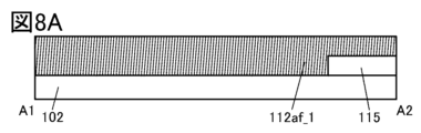
- 8A to 8D are cross-sectional views illustrating an example of a method for manufacturing a transistor.
- FIGS. 9A to 9D are cross-sectional views illustrating an example of a method for manufacturing a transistor.
- 10A to 10C are cross-sectional views showing an example of a transistor.
- 11A and 11B are cross-sectional views showing an example of a transistor.
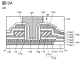
- 12A and 12B are cross-sectional views showing an example of a transistor.
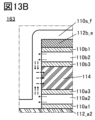
- 13A to 13D are cross-sectional views showing an example of a transistor.
- FIG. 14 is a perspective view showing an example of a display device.
- FIG. 15 is a cross-sectional view showing an example of a display device.
- FIG. 16 is a cross-sectional view showing an example of a display device.
- FIG. 17 is a cross-sectional view showing an example of a display device.
- FIG. 15 is a cross-sectional view showing an example of a display device.
- FIG. 16 is a cross-sectional view showing an example of a display device.
- FIG. 17 is a cross-sectional view
- FIG. 18 is a cross-sectional view showing an example of a display device.
- FIG. 19 is a cross-sectional view showing an example of a display device.
- 20A to 20F are cross-sectional views illustrating an example of a method for manufacturing a display device.
- 21A and 21B are diagrams illustrating an example of the configuration of a display device.
- FIG. 22 is a diagram illustrating a configuration example of a display device.
- FIG. 23 is a diagram showing a configuration example of a display device.
- FIG. 24 is a diagram showing a configuration example of a display device.
- 25A to 25C are diagrams illustrating configuration examples of a display device.
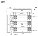
- FIG. 26 is a block diagram of the display device.
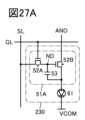
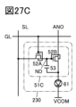
- 27A to 27D are circuit diagrams of pixel circuits.
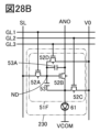
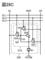
- 28A to 28D are circuit diagrams of pixel circuits.
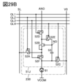
- 29A and 29B are circuit diagrams of pixel circuits.
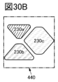
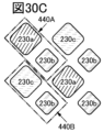
- 30A to 30G are diagrams showing examples of pixels.
- 31A to 31K are diagrams showing examples of pixels.
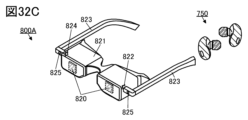
- 32A to 32D are diagrams illustrating an example of an electronic device.
- 33A to 33F are diagrams illustrating an example of an electronic device.
- 34A to 34G are diagrams illustrating an example of an electronic device.
- film and “layer” can be interchanged depending on the situation or circumstances.
- conductive layer can be changed to the term “conductive film.”
- insulating film can be changed to the term “insulating layer.”
- a device manufactured using a metal mask or an FMM may be referred to as a device with an MM (metal mask) structure.
- a device manufactured without using a metal mask or FMM may be referred to as a device with an MML (metal maskless) structure.
- SBS Side By Side
- materials and configurations can be optimized for each light emitting device, which increases the degree of freedom in selecting materials and configurations, making it easier to improve brightness and reliability.
- holes or electrons may be referred to as “carriers.”
- a hole injection layer or an electron injection layer is called a “carrier injection layer”
- a hole transport layer or an electron transport layer is called a “carrier transport layer”
- a hole blocking layer or an electron blocking layer is called a “carrier injection layer.”
- the carrier injection layer, carrier transport layer, and carrier block layer described above may not be clearly distinguishable depending on their respective cross-sectional shapes or characteristics.
- one layer may serve as two or three functions among a carrier injection layer, a carrier transport layer, and a carrier block layer.
- a light emitting device has an EL layer between a pair of electrodes.
- the EL layer has at least a light emitting layer.
- the layers (also referred to as functional layers) included in the EL layer include a light emitting layer, a carrier injection layer (a hole injection layer and an electron injection layer), a carrier transport layer (a hole transport layer and an electron transport layer), and a carrier Block layers (hole block layer and electron block layer) can be mentioned.
- a light-receiving device (also referred to as a light-receiving element) has an active layer that functions as at least a photoelectric conversion layer between a pair of electrodes.
- the term “island-like” refers to a state in which two or more layers made of the same material and formed in the same process are physically separated.
- an island-shaped light emitting layer indicates that the light emitting layer and an adjacent light emitting layer are physically separated.
- the term "tapered shape” refers to a shape in which at least a part of the side surface of the structure is inclined with respect to the substrate surface or the surface to be formed.
- a region where the angle between the inclined side surface and the substrate surface or the surface to be formed (also referred to as a taper angle) is less than 90 degrees, and preferably to have a region where the angle is 45 degrees or more and less than 90 degrees.
- the angle is greater than or equal to 85 degrees, more preferably an area where the angle is greater than or equal to 65 degrees and less than or equal to 85 degrees, further preferably an area where the angle is greater than or equal to 65 degrees and less than or equal to 80 degrees, and even more preferably greater than or equal to 70 degrees and less than or equal to 80 degrees. It is preferable to have a region of less than or equal to 100%. Note that the side surface of the structure, the substrate surface, and the surface to be formed do not necessarily have to be completely flat, and may be substantially planar with a minute curvature or substantially planar with minute irregularities.
- a mask layer also referred to as a sacrificial layer
- a light emitting layer is located above at least a light emitting layer (more specifically, a layer that is processed into an island shape among the layers constituting an EL layer), It has the function of protecting the light emitting layer during the manufacturing process.
- step breakage refers to a phenomenon in which a layer, film, or electrode is separated due to the shape of the surface on which it is formed (for example, a step difference).
- the upper surface shapes roughly match means that at least a portion of the outlines of the stacked layers overlap. For example, this includes a case where the upper layer and the lower layer are processed using the same mask pattern or partially the same mask pattern. However, strictly speaking, the contours may not overlap, and the upper layer may be located inside the lower layer, or the upper layer may be located outside the lower layer, and in this case, it is also said that the top surface shapes approximately match.
- the heights are approximately equal refers to a configuration in which the heights from a reference surface (for example, a flat surface such as a substrate surface) are approximately equal in cross-sectional view.
- a flattening process typically a CMP (Chemical Mechanical Polishing) process
- the heights of surfaces to be processed are approximately the same.
- the heights may not strictly match depending on the material of the film, etc., but in this specification, it is assumed that the heights "approximately match” in this case as well. .
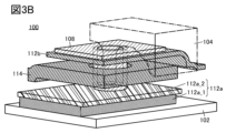
- FIG. 1A A top view (also referred to as a plan view) of the transistor 100 is shown in FIG. 1A.
- FIG. 1B shows a sectional view taken along the dashed-dotted line A1-A2 shown in FIG. 1A
- FIG. 2 shows a sectional view taken along the dashed-dotted line B1-B2.
- FIG. 3A A perspective view of some of the components of the transistor 100 is shown in FIG. 3A, and a perspective view of the transistor 100 is shown in FIG. 3B, respectively.
- FIG. 1A some of the components of the transistor 100 (such as an insulating layer) are omitted.
- FIG. 3B a perspective view of the transistor 100
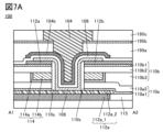
- Transistor 100 is provided on substrate 102.
- the transistor 100 includes a conductive layer 104, an insulating layer 106, a semiconductor layer 108, a conductive layer 114, an insulating layer 110s, a conductive layer 112a, and a conductive layer 112b.
- the conductive layer 104 functions as a gate electrode.
- Conductive layer 114 functions as a second gate electrode.
- a portion of the insulating layer 106 functions as a gate insulating layer.
- the insulating layer 110s functions as a second gate insulating layer.
- the conductive layer 112a functions as one of a source electrode and a drain electrode, and the conductive layer 112b functions as the other.
- the entire region between the source electrode and the drain electrode that overlaps with the gate electrode via the gate insulating layer functions as a channel formation region. Further, in the semiconductor layer 108, a region in contact with the source electrode functions as a source region, and a region in contact with the drain electrode functions as a drain region.
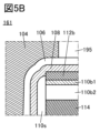
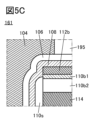
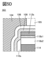
- An insulating layer 115 and a conductive layer 112a are provided on the substrate 102, an insulating layer 110a is provided on the conductive layer 112a, a conductive layer 114 is provided on the insulating layer 110a, and a conductive layer 114 is provided on the insulating layer 110a and the conductive layer 114.
- An insulating layer 110b is provided, and a conductive layer 112b is provided on the insulating layer 110b.
- the insulating layer 110a and the insulating layer 110b have a region sandwiched between the conductive layer 112a and the conductive layer 112b.
- the conductive layer 112a has a region overlapping with the conductive layer 112b via the insulating layer 110a and the insulating layer 110b.
- the insulating layer 110a has a stacked structure of an insulating layer 110a1 and an insulating layer 110a2 on the insulating layer 110a1.
- the insulating layer 110b has a stacked structure of an insulating layer 110b2 and an insulating layer 110b1 on the insulating layer 110b2.
- the conductive layer 114 has a region sandwiched between an insulating layer 110a2 and an insulating layer 110b2.
- the insulating layer 110a2 has a region in contact with the lower surface of the conductive layer 114.
- the insulating layer 110b2 is in contact with the upper surface of the conductive layer 114, for example.
- the insulating layer 110a, the conductive layer 114, the insulating layer 110b, and the conductive layer 112b each have an opening.
- Each opening has, for example, a region that overlaps with the conductive layer 112a.
- the insulating layer 110s is provided on the conductive layer 112a.
- the insulating layer 110s includes an opening in the insulating layer 110a (area not shown in the figure), an opening 142 in the conductive layer 114, an opening in the insulating layer 110b (area not shown in the figure), and an opening in the conductive layer 112b. 143 along each side wall.
- the side walls of the openings of the insulating layer 110a, the conductive layer 114, the insulating layer 110b, and the conductive layer 112b form a continuous side surface, and the insulating layer 110s is formed along the continuous side surface. is formed.
- the insulating layer 110s is sometimes called a sidewall, a sidewall insulating layer, a sidewall protective layer, or the like.
- the opening 142 and the opening 143 each have a region that overlaps with the conductive layer 112a. Further, the opening 142 and the opening 143 have regions that overlap with each other.
- the semiconductor layer 108 is provided along a recess (sometimes called a depression) whose bottom is the upper surface of the conductive layer 112a and whose inner wall is the side wall 141 of the insulating layer 110s.
- the semiconductor layer 108 overlaps with the conductive layer 112a in a region inside the sidewall 141 of the insulating layer 110s in plan view. In this region, the semiconductor layer 108 contacts, for example, the upper surface of the conductive layer 112a.
- the semiconductor layer 108 overlaps with the conductive layer 112b in a region outside the side wall 141 of the insulating layer 110s in plan view. In this region, the semiconductor layer 108 contacts, for example, the upper surface of the conductive layer 112b.
- the transistor 100 can be called a bottom contact transistor because the lower surface of the semiconductor layer 108 is in contact with the source electrode and the drain electrode.
- the semiconductor layer 108 has a region provided along the top surface of the conductive layer 112a, a region provided along the sidewall 141 of the insulating layer 110s, and a region provided along the top surface of the conductive layer 112b.
- the semiconductor layer 108 has a region facing the sidewall of the opening 142 with the insulating layer 110s interposed therebetween. Further, in this region, the semiconductor layer 108 is preferably in contact with the side wall 141 of the insulating layer 110s.
- FIG. 1B It may be a layer.
- a common material is used in several components that are successive layers.
- multiple components in one continuous layer may be fabricated, for example, in the same step.
- multiple components may be observed as one continuous layer.
- the insulating layer 110a2 and the insulating layer 110s may be observed as a continuous layer.
- the insulating layer 110b2 and the insulating layer 110s may be observed as a continuous layer.
- FIG. 4 shows an example of a cross section when the insulating layer 110a2, the insulating layer 110b2, and the insulating layer 110s are observed as a continuous layer (indicated as an insulating layer 110_2 in FIG. 4).
- the conductive layer 112a and the conductive layer 112b may each have a stacked structure.
- the conductive layer 112a has a stacked structure of a conductive layer 112a_1 and a conductive layer 112a_2 over the conductive layer 112a_1.
- the conductive layer 112a_1 is embedded in the opening of the insulating layer 115, and the upper surface of the conductive layer 112a_1 and the upper surface of the insulating layer 115 are flattened.
- the conductive layer 112a_2 is located on the conductive layer 112a_1 and the insulating layer 115.
- the structure is such that the height of the top surface of the insulating layer 115 and the height of the top surface of the conductive layer 112a_1 approximately match.
- FIG. 1B etc. show an example in which the end of the conductive layer 112a_2 is located outside the end of the conductive layer 112a_1, the end of the conductive layer 112a_2 is located inside the end of the conductive layer 112a_1. You may. Further, in the case of providing a plug that connects the conductive layer 112a and the upper conductive layer, the conductive layer 112a_1 is extended to the outside of the conductive layer 112a_2, and in the extended region, the upper surface of the conductive layer 112a_1 and the plug are It is also possible to have a configuration in which the two are in contact with each other. The plug is provided so as to fill the openings in the insulating layer 110a, the insulating layer 110b, the insulating layer 195, etc.
- An insulating layer 106 is provided on the semiconductor layer 108.
- the insulating layer 106 has a region overlapping with the conductive layer 112a with the semiconductor layer 108 in between, a region overlapping with the conductive layer 114 with the semiconductor layer 108 and the insulating layer 110s in between, and a region with the semiconductor layer 108 in between. and a region overlapping with the conductive layer 112b.
- the insulating layer 106 has a region facing the upper surface of the conductive layer 112a with the semiconductor layer 108 in between, and a region facing the side surface of the conductive layer 114 with the semiconductor layer 108 and the insulating layer 110s in between. and a region facing the upper surface of the conductive layer 112b with the semiconductor layer 108 therebetween.
- An insulating layer 195 is provided to cover the conductive layer 112a, the semiconductor layer 108, the conductive layer 112b, the insulating layer 106, and the like of the transistor 100.
- the insulating layer 195 functions as a protective layer for the transistor 100.
- a conductive layer 104 is provided on the insulating layer 106.
- the conductive layer 104 has a region that overlaps with the semiconductor layer 108 between the conductive layers 112a and 112b with the insulating layer 106 interposed therebetween. Further, the conductive layer 104 has a region overlapping with the conductive layer 114 with the insulating layer 106, the semiconductor layer 108, and the insulating layer 110s interposed therebetween.
- an insulating layer 106 is provided between the conductive layer 104 and the conductive layer 112a. Further, in a region of the transistor 100 where the conductive layer 104 and the conductive layer 112b are insulated, for example, an insulating layer 106 is provided between the conductive layer 104 and the conductive layer 112b.
- the semiconductor layer 108 is provided along a recess whose bottom is the upper surface of the conductive layer 112a and whose inner wall is the side wall 141 of the insulating layer 110s, and the upper surface of the semiconductor layer 108 has a recess.
- the insulating layer 106 is provided on the semiconductor layer 108, and the upper surface of the insulating layer 106 has a recessed portion.
- the conductive layer 104 is provided so as to fill the recess. Thereby, the conductive layer 104 can be made thicker, and the electrical resistance can be lowered.
- the conductive layer 104 is provided so as to fill the opening of the insulating layer 195, and the upper surfaces of the conductive layer 104 and the insulating layer 195 are substantially aligned.
- one of the conductive layer 104 and the conductive layer 114 can function as a gate, and the other can function as a back gate.
- the conductive layer 104 and the conductive layer 114 are preferably arranged to sandwich the channel formation region of the semiconductor layer 108.
- the field effect mobility of the transistor can be increased. Further, by changing the potential of the back gate, the threshold voltage of the transistor can be changed.
- the potential of the back gate can be the same as that of the gate. Alternatively, the potential of the back gate may be a ground potential or an arbitrary potential. Further, the potential of the back gate may be set to be the same potential as the source or drain.
- the back gate and the gate When applying the same potential to the back gate as the gate, the back gate and the gate may be electrically connected and conductive.
- the back gate and the source or drain When applying the same potential to the back gate as the source or drain, the back gate and the source or drain may be electrically connected and conductive.
- reliability can be improved by configuring the gate or back gate to be electrically connected to the source.
- the transistor can function as a diode, for example.
- a common wiring electrically connected to the back gates of a plurality of transistors may be provided and the potential may be applied to the common wiring.
- variations in characteristics among a plurality of transistors can be reduced in some cases.
- variations in threshold values among a plurality of transistors can be reduced in some cases.
- the upper surface shapes of the opening 142, the opening 143, and the side wall 141 can each be, for example, circular or elliptical.
- the upper surface shapes of the opening 142, the opening 143, and the side wall 141 may each be a polygon such as a triangle, a quadrangle (including a rectangle, a rhombus, and a square), a pentagon, or a shape with rounded corners of these polygons.
- the upper surfaces of the openings 142 and 143 are preferably circular.
- the upper surface shapes of the openings 142 and 143 By making the upper surface shapes of the openings 142 and 143 circular, it is possible to improve the processing accuracy when forming the openings 142 and 143, and it is possible to form the openings 142 and 143 with minute sizes. Note that in this specification and the like, circular is not limited to a perfect circle.
- the top surface shape of the side wall 141 of the insulating layer 110s changes depending on the shape of the opening in the insulating layer 110a, the opening 142 in the conductive layer 114, the opening in the insulating layer 110b, and the opening 143 in the conductive layer 112b. .
- the top surface shape of the side wall 141 can also be made circular.
- the coverage of the semiconductor layer 108 provided along the side wall 141 can be improved.
- the thickness of the semiconductor layer 108 and the insulation formed on the semiconductor layer 108 in the corner region are smaller than in the region where the upper surface is a straight line or a circle.
- the thickness of layer 106 may be non-uniform.
- electric field concentration will occur between the semiconductor layer 108 and the gate electrode in a region where the film thickness is non-uniform. Electric field concentration may cause deterioration of the transistor.
- the opening of the insulating layer 110a, the opening 142 of the conductive layer 114, the opening of the insulating layer 110b, and the opening 143 of the conductive layer 112b are formed, for example, by forming a mask on the surface to be processed and using an etching process. be able to.
- a resist mask may be used as the mask, or a hard mask made of an insulating layer or a conductive layer may be used.
- the opening 143 in the conductive layer 112b, the opening in the insulating layer 110b, the opening 142 in the conductive layer 114, and the opening in the insulating layer 110a are successively formed, and then the mask is removed. This can also serve as a mask forming process, and the diameters of the respective openings can also be made approximately the same.
- the process of successively forming a plurality of openings using the same mask may be referred to as batch opening.
- the configuration shown in FIG. 1B, FIG. 2, etc. can be manufactured.
- the step of forming the openings by approximately matching the diameters of the respective openings, the coverage of the insulating layer 110s can be improved.
- the openings in the insulating layer 110a, the openings 142 in the conductive layer 114, the openings in the insulating layer 110b, and the openings 143 in the conductive layer 112b do not have to be formed continuously.
- a mask may be formed when each opening is provided.
- FIG. 3A is a perspective view showing a portion of each component of the transistor 100.
- FIG. 3B is a perspective view of the transistor 100 on the substrate 102. Note that in FIG. 3B, among the components of the transistor 100, the conductive layer 112a, the conductive layer 114, the semiconductor layer 108, the conductive layer 112b, and the conductive layer 104 are shown, and the insulating layers such as the insulating layer 110s and the insulating layer 106 are not shown. Not yet. Furthermore, in order to make other components easier to see, the conductive layer 104 is shown with broken lines.
- the channel length and channel width of the transistor 100 will be explained.
- the region in contact with the conductive layer 112a functions as one of the source region and the drain region
- the region in contact with the conductive layer 112b functions as the other of the source region and the drain region
- the region between the source region and the drain region functions as a channel forming region.
- the channel length of transistor 100 is the distance between the source and drain regions.
- the channel length L100 of the transistor 100 is indicated by a dashed double-headed arrow.
- the channel length L100 is the length of the side surface and the top surface of the insulating layer 110s.
- the channel length L100 of the transistor 100 is the sum of the thickness of the insulating layer 110a, the thickness of the conductive layer 114, and the thickness of the insulating layer 110b in a region sandwiched between the upper surface of the conductive layer 112a and the lower surface of the conductive layer 112b.
- a thickness T110 (the thickness T110 is indicated by a double-dashed dashed arrow in FIGS. 1B and 2) may be used.
- the sum of the thickness T110 and the thickness of the conductive layer 112b may be used as the channel length L100 of the transistor 100.
- the channel length L100 of the transistor 100 is determined by the thickness of the insulating layer 110a, the thickness of the conductive layer 114, the thickness of the insulating layer 110b, the thickness of the insulating layer 110s, the sidewall 141 of the insulating layer 110s, and the thickness of the insulating layer 110a. It is determined by the angle ⁇ 110 formed with the surface to be formed (in this case, the upper surface of the conductive layer 112a), and is not affected by the performance of the exposure apparatus used for manufacturing the transistor. Therefore, the channel length L100 can be set to a value smaller than the limit resolution of the exposure apparatus, and a fine-sized transistor can be realized.
- the channel length L100 is preferably 500 nm or less, 200 nm or less, 100 nm or less, 60 nm or less, 50 nm or less, 40 nm or less, 30 nm or less, 20 nm or less, or 10 nm or less, and preferably 1 nm or more, or 5 nm or more.
- the thickness T110 is preferably 1 ⁇ m or less, 500 nm or less, 200 nm or less, 100 nm or less, 60 nm or less, 50 nm or less, 40 nm or less, 30 nm or less, 20 nm or less, or 10 nm or less, and preferably 1 nm or more, or 5 nm or more.
- the angle between the conductive layer 112a and the surface on which the insulating layer 110s is formed is defined as an angle ⁇ 110. It is preferable that the angle ⁇ 110 is approximately 90 degrees or close to 90 degrees. Specifically, for example, the angle ⁇ 110 is, for example, 60 degrees or more and 115 degrees or less, preferably 70 degrees or more and 105 degrees or less, and more preferably 80 degrees or more and 95 degrees or less.
- the insulating layer 110s can be selectively formed on the side surfaces of the insulating layer 110a, the conductive layer 114, and the insulating layer 110b in the process of forming the insulating layer 110s (for example, an etch-back process). can remain.
- the insulating layer 110s may not follow all areas of the sidewalls of the openings of the insulating layer 110a, the conductive layer 114, the insulating layer 110b, and the conductive layer 112b.
- the opening 112b may be provided along only a part of the side wall of the opening 143.
- FIG. 5A is an enlarged view of region 161 shown in FIG. 1B.
- FIG. 5A shows a configuration in which the height of the top surface of the insulating layer 110s approximately matches the height of the top surface of the conductive layer 112b.
- 5B and 5C are examples of configurations that differ from FIG. 5A in the height of the upper surface of the insulating layer 110s, etc.
- FIG. 5B shows a configuration in which the height of the top surface of the insulating layer 110s is lower than the height of the top surface of the conductive layer 112b and higher than the height of the top surface of the insulating layer 110b1 located below the conductive layer 112b.
- the side surface of the conductive layer 112b has a region in contact with the semiconductor layer 108.
- the contact area between the semiconductor layer 108 and the conductive layer 112b is increased, and the resistance may be reduced.
- FIG. 5C shows a configuration in which the height of the top surface of the insulating layer 110s is lower than the height of the top surface of the insulating layer 110b1.
- the side surface of the conductive layer 112b has a region in contact with the semiconductor layer 108
- the side surface of the insulating layer 110b1 has a region in contact with the semiconductor layer 108.
- FIG. 5D shows a configuration in which the height of the top surface of the insulating layer 110s is lower than the height of the top surface of the insulating layer 110b2.
- the side surface of the conductive layer 112b has a region in contact with the semiconductor layer 108
- the side surface of the insulating layer 110b1 has a region in contact with the semiconductor layer 108
- the side surface of the insulating layer 110b2 has a region in contact with the semiconductor layer 108. It has a region in contact with the semiconductor layer 108.
- the thickness of the insulating layer 110s may be reduced by lengthening the etching time.
- the height of the upper surface of the insulating layer 110s may become lower than the height of the conductive layer 112b.
- the height of the top surface of the insulating layer 110s is preferably higher than at least the height of the top surface of the conductive layer 114.
- the on-state current of the transistor 100 can be increased.
- the transistor 100 By using the transistor 100, a circuit that can operate at high speed can be manufactured. Furthermore, it becomes possible to reduce the area occupied by the circuit. Therefore, when the transistor of one embodiment of the present invention is applied to a semiconductor device, the device can be miniaturized.
- the frame of the display device can be made narrower.
- the transistor of one embodiment of the present invention when applied to a large display device or a high-definition display device, even if the number of wires increases, signal delay in each wire can be reduced, and display unevenness can be reduced. can be suppressed.
- the channel width of the transistor 100 is the width of the source region or the width of the drain region in the direction perpendicular to the channel length direction.
- the channel width is the width of the region where the semiconductor layer 108 and the conductive layer 112a are in contact, or the width of the region where the semiconductor layer 108 and the conductive layer 112b are in contact in the direction perpendicular to the channel length direction.
- the semiconductor layer 108 is provided along a concave portion whose bottom is the upper surface of the conductive layer 112a and whose inner wall is the side wall 141 of the insulating layer 110s. Therefore, the circumference of the inner wall of the side wall 141 of the insulating layer 110s in plan view may be used as the channel width.
- the insulating layer 110s can also be expressed as having a shape having an opening at or near the center of a cylinder, for example. The circumference of the opening can also be used as the channel width of the semiconductor layer 108.
- the channel width of the transistor 100 will be described as the width of a region where the semiconductor layer 108 and the conductive layer 112b are in contact with each other in a direction perpendicular to the channel length direction.
- the channel width W100 of the transistor 100 is indicated by a solid double-headed arrow.
- the channel width W100 is the length of the opening 143 when viewed from above.
- the channel width W100 is determined by the top shape of the opening 143.
- the width D143 of the opening 143 is indicated by a two-dot chain double-headed arrow.
- the width D143 refers to the short side of the smallest rectangle circumscribing the opening 143 when viewed from above.
- the width D143 of the opening 143 is equal to or larger than the resolution limit of the exposure apparatus.
- the width D143 is, for example, 0.20 ⁇ m or more and less than 5.0 ⁇ m. Note that when the top surface shape of the opening 143 is circular, the width D143 corresponds to the diameter of the opening 143, and the channel width W100 can be calculated as "D143 ⁇ ".
- the semiconductor material that can be used for the semiconductor layer 108 is not particularly limited.
- an elemental semiconductor or a compound semiconductor can be used.
- silicon or germanium can be used as the single semiconductor.
- the compound semiconductor include gallium arsenide and silicon germanium.
- an organic substance having semiconductor properties or a metal oxide having semiconductor properties also referred to as an oxide semiconductor
- these semiconductor materials may contain impurities as dopants.
- the crystallinity of the semiconductor material used for the semiconductor layer 108 is not particularly limited; ) may be used. It is preferable to use a semiconductor having crystallinity because deterioration of transistor characteristics can be suppressed.
- Silicon can be used for the semiconductor layer 108.
- Examples of silicon include single crystal silicon, polycrystalline silicon, microcrystalline silicon, and amorphous silicon.
- Examples of polycrystalline silicon include low temperature polysilicon (LTPS).
- a transistor using amorphous silicon for the semiconductor layer 108 can be formed over a large glass substrate and can be manufactured at low cost.
- a transistor using polycrystalline silicon for the semiconductor layer 108 has high field effect mobility and can operate at high speed.
- a transistor using microcrystalline silicon for the semiconductor layer 108 has higher field effect mobility than a transistor using amorphous silicon, and can operate at high speed.
- the semiconductor layer 108 preferably includes a metal oxide (oxide semiconductor).
- metal oxides that can be used for the semiconductor layer 108 include indium oxide, gallium oxide, and zinc oxide.
- the metal oxide contains at least indium (In) or zinc (Zn).
- the metal oxide has two or three selected from indium, element M, and zinc.
- element M is gallium, aluminum, silicon, boron, yttrium, tin, copper, vanadium, beryllium, titanium, iron, nickel, germanium, zirconium, molybdenum, lanthanum, cerium, neodymium, hafnium, tantalum, tungsten, cobalt, and magnesium.
- the element M is preferably one or more selected from aluminum, gallium, yttrium, and tin. Element M is more preferably gallium.
- the semiconductor layer 108 is made of, for example, indium oxide, indium zinc oxide (In-Zn oxide), indium tin oxide (In-Sn oxide), indium titanium oxide (In-Ti oxide), or indium aluminum zinc oxide.
- In-Al-Zn oxide, also written as IAZO indium tin zinc oxide (In-Sn-Zn oxide), indium titanium zinc oxide (In-Ti-Zn oxide), indium gallium zinc oxide (In-Ga-Zn oxide, also written as IGZO), indium gallium tin zinc oxide (In-Ga-Sn-Zn oxide, also written as IGZTO), indium gallium aluminum zinc oxide (In-Ga-Al-Zn oxide (also referred to as IGAZO or IAGZO), etc. can be used.
- indium tin oxide containing silicon or the like can be used.
- a sputtering method or an atomic layer deposition (ALD) method can be suitably used to form the metal oxide.
- the atomic ratio of the target and the atomic ratio of the metal oxide may be different.
- the atomic ratio of the metal oxide may be smaller than the atomic ratio of the target.
- the atomic ratio of zinc contained in the target may be about 40% or more and 90% or less.
- a specific example of forming the semiconductor layer 108 using an atomic layer deposition (ALD) method is a thermal ALD (atomic layer deposition) method or a PEALD (plasma enhanced ALD) method.
- ALD atomic layer deposition
- PEALD plasma enhanced ALD
- Membrane method can be used preferable.
- the thermal ALD method is preferable because it shows extremely high step coverage.
- the PEALD method is preferable because it not only shows high step coverage but also enables low-temperature film formation.
- composition of the metal oxide included in the semiconductor layer 108 greatly affects the electrical characteristics and reliability of the transistor 100.
- a transistor with a large on-current can be realized.
- a metal oxide that does not contain gallium or has a low gallium content in the semiconductor layer 108 a transistor that has high reliability against application of a positive bias can be obtained.
- a metal oxide with a low content of element M for the semiconductor layer 108 a transistor with high reliability against application of a positive bias can be obtained.
- a transistor with high reliability against light can be obtained.
- the semiconductor layer 108 is preferably a metal oxide layer having crystallinity.
- a metal oxide layer having a CAAC (c-axis aligned crystal) structure, a polycrystalline structure, a microcrystalline (NC: nano-crystal) structure, etc. can be used.
- CAAC c-axis aligned crystal
- NC microcrystalline
- the density of defect levels in the semiconductor layer 108 can be reduced, and a highly reliable transistor can be realized.
- the semiconductor layer 108 may have a stacked structure of two or more metal oxide layers having different crystallinities.
- the layered structure includes a first metal oxide layer and a second metal oxide layer provided on the first metal oxide layer, and the second metal oxide layer
- the structure can include a region having higher crystallinity than the oxide layer.
- the second metal oxide layer may have a region having lower crystallinity than the first metal oxide layer.
- the two or more metal oxide layers included in the semiconductor layer 108 may have the same or approximately the same composition. By forming a stacked structure of metal oxide layers having the same composition, for example, the same sputtering target can be used to form the layers, thereby reducing manufacturing costs.
- a stacked structure of two or more metal oxide layers having different crystallinity can be formed.
- the two or more metal oxide layers included in the semiconductor layer 108 may have different compositions.
- the thickness of the semiconductor layer 108 is preferably 3 nm or more and 100 nm or less, more preferably 5 nm or more and 100 nm or less, further preferably 10 nm or more and 100 nm or less, further preferably 10 nm or more and 70 nm or less, and even more preferably 15 nm or more and 70 nm or less. , more preferably 15 nm or more and 50 nm or less, further preferably 20 nm or more and 50 nm or less, further preferably 20 nm or more and 40 nm or less, and even more preferably 25 nm or more and 40 nm or less.
- V O oxygen vacancies
- a defect in which hydrogen is present in an oxygen vacancy (hereinafter referred to as V OH ) functions as a donor, and electrons, which are carriers, may be generated.
- a portion of hydrogen may combine with oxygen that is bonded to a metal atom to generate electrons, which are carriers. Therefore, a transistor using an oxide semiconductor containing a large amount of hydrogen tends to have normally-on characteristics. Further, since hydrogen in an oxide semiconductor is easily moved by stress such as heat or an electric field, if the oxide semiconductor contains a large amount of hydrogen, the reliability of the transistor may deteriorate.
- V OH can function as a donor for the oxide semiconductor.
- V OH in the semiconductor layer 108 when an oxide semiconductor is used for the semiconductor layer 108, it is preferable to reduce V OH in the semiconductor layer 108 as much as possible to make the semiconductor layer 108 highly pure or substantially pure.
- impurities such as water and hydrogen in the oxide semiconductor are removed (sometimes referred to as dehydration or dehydrogenation treatment). Therefore, it is important to supply oxygen to the oxide semiconductor to repair oxygen vacancies (V O ).
- an oxide semiconductor in which impurities such as V OH are sufficiently reduced for a channel formation region of a transistor stable electrical characteristics can be provided. Note that supplying oxygen to an oxide semiconductor to repair oxygen vacancies (V O ) may be referred to as oxygenation treatment.
- the carrier concentration of the oxide semiconductor in a region functioning as a channel formation region is preferably 1 ⁇ 10 18 cm ⁇ 3 or less, and less than 1 ⁇ 10 17 cm ⁇ 3 . More preferably, it is less than 1 ⁇ 10 16 cm ⁇ 3 , even more preferably less than 1 ⁇ 10 13 cm ⁇ 3 , even more preferably less than 1 ⁇ 10 12 cm ⁇ 3 .
- the lower limit of the carrier concentration of the oxide semiconductor in the region functioning as a channel formation region is not particularly limited, but can be set to 1 ⁇ 10 ⁇ 9 cm ⁇ 3 , for example.
- a transistor using an oxide semiconductor (hereinafter referred to as an OS transistor) has extremely high field effect mobility compared to a transistor using amorphous silicon.
- OS transistors have extremely low source-drain leakage current (hereinafter also referred to as off-state current) in the off state, and can retain the charge accumulated in the capacitor connected in series with the transistor for a long period of time. is possible. Further, by applying an OS transistor to a semiconductor device, power consumption of the semiconductor device can be reduced.
- OS transistors can be applied to display devices.
- a light emitting device included in a pixel circuit of a display device it is necessary to increase the amount of current flowing through the light emitting device.
- the source-drain voltage of the drive transistor included in the pixel circuit Since an OS transistor has a higher breakdown voltage between the source and drain than a transistor using silicon (hereinafter referred to as a Si transistor), a high voltage can be applied between the source and drain of the OS transistor. Therefore, by applying the OS transistor to the drive transistor of the pixel circuit, the amount of current flowing through the light emitting device can be increased, and the luminance of the light emitting device can be increased.
- an OS transistor When a transistor operates in a saturation region, an OS transistor can make a change in source-drain current smaller than a Si transistor with respect to a change in gate-source voltage. Therefore, by applying an OS transistor as a drive transistor included in a pixel circuit, the current flowing between the source and drain can be precisely determined by changing the gate-source voltage, so the amount of current flowing through the light emitting device can be controlled. It can be precisely controlled. Therefore, the number of gradations in the pixel circuit can be increased.
- OS transistors are able to flow a more stable current (saturation current) than Si transistors even when the source-drain voltage gradually increases. can. Therefore, by using an OS transistor as a drive transistor, a stable current can be passed through the light-emitting device even if, for example, there are variations in the current-voltage characteristics of the light-emitting device. That is, when the OS transistor operates in the saturation region, the source-drain current does not substantially change even if the source-drain voltage is increased, so that the luminance of the light-emitting device can be stabilized.
- OS transistors as drive transistors included in pixel circuits, it is possible to "suppress black floating,” “increase luminance,” “multiple gradations,” and “suppress variations in light-emitting devices.” can be achieved.
- OS transistors have small variations in electrical characteristics due to radiation irradiation, that is, have high resistance to radiation, and therefore can be suitably used even in environments where radiation may be incident. It can also be said that OS transistors have high reliability against radiation.
- an OS transistor can be suitably used in a pixel circuit of an X-ray flat panel detector.
- OS transistors can be suitably used in semiconductor devices used in outer space. Radiation includes electromagnetic radiation (eg, x-rays, and gamma rays), and particle radiation (eg, alpha, beta, neutron, and proton radiation).
- an inorganic insulating material or an organic insulating material can be used as the insulating layer.
- a laminated structure of an inorganic insulating material and an organic insulating material may be used as the insulating layer.
- the inorganic insulating material one or more of oxides, oxynitrides, nitrided oxides, and nitrides can be used.
- oxynitride refers to a material whose composition contains more oxygen than nitrogen.
- a nitrided oxide refers to a material whose composition contains more nitrogen than oxygen.
- silicon oxynitride refers to a material whose composition contains more oxygen than nitrogen
- silicon nitride oxide refers to a material whose composition contains more nitrogen than oxygen.
- the content of oxygen and nitrogen can be analyzed using, for example, secondary ion mass spectrometry (SIMS) or X-ray photoelectron spectroscopy (XPS).
- SIMS secondary ion mass spectrometry
- XPS X-ray photoelectron spectroscopy
- the film density of the insulating layer or the like can be evaluated using, for example, Rutherford Backscattering Spectrometry (RBS) or X-Ray Reflection (XRR). Further, the difference in film density may be evaluated using a cross-sectional transmission electron microscopy (TEM) image.
- TEM transmission electron microscopy
- the nitrogen content of the insulating layer can be confirmed by, for example, EDX.
- EDX EDX-ray electron spectroscopy
- the nitrogen content can be evaluated using the ratio of the peak height of nitrogen to the peak height of silicon.
- the peak of a certain element is the peak of a certain element when the count number of the element reaches the maximum value in the spectrum where the horizontal axis shows the energy of the characteristic X-ray and the vertical axis shows the count number (detected value) of the characteristic X-ray.
- the difference in nitrogen content may be confirmed by the ratio of the count number of nitrogen to the count number of silicon using the count number at the energy of the characteristic X-ray unique to the element. For example, counts at 1.739 keV (Si-K ⁇ ) can be used for silicon, and counts at 0.392 keV (N-K ⁇ ) can be used for nitrogen.
- the hydrogen concentration in the insulating layer can be evaluated by, for example, secondary ion mass spectrometry (SIMS).
- SIMS secondary ion mass spectrometry
- oxygen can be supplied from the insulating layer to the semiconductor layer 108.
- oxygen vacancies (V O ) and V O H in the semiconductor layer 108 can be reduced, and a transistor exhibiting good electrical characteristics and high reliability can be obtained. It can be done.
- the treatment for supplying oxygen to the semiconductor layer 108 includes heat treatment in an atmosphere containing oxygen, plasma treatment in an atmosphere containing oxygen, and the like.
- Oxygen vacancies (V O ) and V OH in the channel formation region of the transistor 100 are preferably small.
- the channel length L100 when the channel length L100 is short, the influence of oxygen vacancies (V O ) and V O H in the channel forming region on the electrical characteristics and reliability becomes large.
- the carrier concentration in the channel formation region increases due to the diffusion of V OH from the source region or the drain region to the channel formation region, which may cause a fluctuation in the threshold voltage of the transistor 100 or a decrease in reliability.
- the shorter the channel length L100 of the transistor 100 the greater the influence of such V O H diffusion on the electrical characteristics and reliability.
- the insulating layer in contact with the semiconductor layer 108 or the insulating layer located around the semiconductor layer 108 preferably releases little impurity (for example, water and hydrogen) from itself.
- impurity for example, water and hydrogen
- Oxygen may be desorbed from the semiconductor layer 108 due to heat applied in steps subsequent to the formation of the semiconductor layer 108.
- the increase in oxygen vacancies (V O ) and V O H is suppressed. be able to.
- the degree of freedom in processing temperature can be increased in steps subsequent to the formation of the semiconductor layer 108. Specifically, the processing temperature can be increased even in steps subsequent to the formation of the semiconductor layer 108. Therefore, the transistor 100 exhibiting good electrical characteristics and high reliability can be formed.
- Insulating layer 110a, insulating layer 110b An inorganic insulating material or an organic insulating material can be used as the insulating layer 110a and the insulating layer 110b, respectively.
- the insulating layer 110a and the insulating layer 110b may have a laminated structure of an inorganic insulating material and an organic insulating material.
- An inorganic insulating material can be suitably used as the insulating layer 110a and the insulating layer 110b.
- the inorganic insulating material one or more of oxides, oxynitrides, nitrided oxides, and nitrides can be used.
- the insulating layer 110a and the insulating layer 110b include silicon oxide, silicon oxynitride, aluminum oxide, hafnium oxide, yttrium oxide, zirconium oxide, gallium oxide, tantalum oxide, magnesium oxide, lanthanum oxide, cerium oxide, neodymium oxide, silicon nitride, One or more of silicon nitride oxide and aluminum nitride can be used.
- the insulating layer 110a and the insulating layer 110b may have a stacked structure of two or more layers.
- the insulating layer 110a has a stacked structure of an insulating layer 110a1 and an insulating layer 110a2 on the insulating layer 110a1
- the insulating layer 110b has a stacked structure of an insulating layer 110b2 and an insulating layer 110b1 on the insulating layer 110b2.
- a configuration having a laminated structure is shown.
- the insulating layer 110a1, the insulating layer 110a2, the insulating layer 110b2, and the insulating layer 110b1 can each use a material that can be used for the above-described insulating layer 110a and insulating layer 110b. Note that the insulating layer 110a1, the insulating layer 110a2, the insulating layer 110b2, and the insulating layer 110b1 may use the same material or different materials.
- the insulating layer 110a1, the insulating layer 110a2, the insulating layer 110b2, and the insulating layer 110b1 release little impurity (for example, water and hydrogen) from themselves.
- the thickness of the insulating layer 110a2 can be configured to be thicker than the thickness of the insulating layer 110a1. Further, the thickness of the insulating layer 110b2 can be configured to be thicker than the thickness of the insulating layer 110b1.
- the deposition rate of the insulating layer 110a2 is preferably fast. By increasing the deposition rate of a thick film, productivity can be increased.
- the insulating layer 110a1 and the insulating layer 110b1 function as blocking films that suppress desorption of gas from the insulating layer 110a2 and the insulating layer 110b1, respectively. It is preferable that the insulating layer 110a1 and the insulating layer 110b1 are each made of a material that does not easily diffuse gas. It is preferable that the insulating layer 110a1 has a region having a higher film density than the insulating layer 110a2. Further, it is preferable that the insulating layer 110b1 has a region having a higher film density than the insulating layer 110b2. Blocking properties can be improved by increasing the film density of the insulating layer. By slowing down the deposition rate of the insulating layer, the film density can be increased and blocking properties can be improved.
- an oxide or an oxynitride for the insulating layer 110a2 and the insulating layer 110b2. It is preferable to use a film that releases oxygen when heated as the insulating layer 110a2 and the insulating layer 110b2.
- silicon oxide or silicon oxynitride can be suitably used as the insulating layer 110a2 and the insulating layer 110b2.
- the insulating layer 110a2 and the insulating layer 110b2 release oxygen, oxygen can be supplied from the insulating layer 110a2 and the insulating layer 110b2 to the semiconductor layer 108.
- the insulating layer 110a2 and the insulating layer 110b2 preferably have a high oxygen diffusion coefficient. By increasing the diffusion coefficient of oxygen, oxygen can be easily diffused in the insulating layer 110b, and oxygen can be efficiently supplied to the semiconductor layer 108.
- the insulating layer 110a1, the insulating layer 110a2, the insulating layer 110b1, and the insulating layer 110b2 are preferably formed by a film formation method such as a sputtering method, an ALD method, or a plasma CVD method.
- the film can be formed using a silicon target in an atmosphere containing an oxidizing gas.
- silicon nitride is formed by a sputtering method
- the film can be formed using a silicon target in an atmosphere containing nitrogen gas, for example.
- the film can be formed using an aluminum target in an atmosphere containing an oxidizing gas.
- silicon oxide and silicon nitride can be formed using, for example, the PEALD method.
- aluminum oxide and hafnium oxide can be formed into films using, for example, a thermal ALD method.
- the insulating layer 110a1 a material containing more nitrogen than the insulating layer 110a2 can be used. Further, the insulating layer 110b1 can be made of a material containing more nitrogen than the insulating layer 110b2. Blocking properties can be improved by increasing the nitrogen content of the insulating layer.
- the insulating layer 110a1 may have a region where the hydrogen concentration in the film is lower than that of the insulating layer 110a2.
- the insulating layer 110b1 may have a region where the hydrogen concentration in the film is lower than that of the insulating layer 110b2.
- the insulating layer 110a1 and the insulating layer 110b1 each have difficulty in transmitting oxygen.
- the insulating layer 110a1 and the insulating layer 110b1 function as a blocking film that suppresses desorption of oxygen from the insulating layer 110a2 and the insulating layer 110b2. Further, it is preferable that each of the insulating layer 110a1 and the insulating layer 110b1 is difficult to transmit hydrogen.
- the insulating layer 110a1 and the insulating layer 110b1 function as a blocking film that suppresses hydrogen from diffusing from outside the transistor to the semiconductor layer 108 through the insulating layer 110a1 and the insulating layer 110b1.
- the film density of the insulating layer 110a1 and the insulating layer 110b1 is high. By increasing the film density, oxygen and hydrogen blocking properties can be improved.
- silicon oxide or silicon oxynitride is used for the insulating layer 110a2 and the insulating layer 110b2
- silicon nitride or silicon nitride oxide can be used for the insulating layer 110a1 and the insulating layer 110b1, respectively.
- hafnium oxide or aluminum oxide can be suitably used as the insulating layer 110a1 and the insulating layer 110b1.
- insulating layer 110a1 and the insulating layer 110b1 a structure in which two or more layers selected from silicon nitride, silicon nitride oxide, hafnium oxide, and aluminum oxide are stacked can be used, respectively.
- oxygen contained in the insulating layer 110b2 diffuses upward from a region of the insulating layer 110b2 that is not in contact with the semiconductor layer 108 (for example, the upper surface of the insulating layer 110b2), the amount of oxygen supplied from the insulating layer 110b2 to the semiconductor layer 108 increases. It may become less.
- oxygen contained in the insulating layer 110b2 can be suppressed from diffusing from a region of the insulating layer 110b2 that is not in contact with the semiconductor layer 108.
- the insulating layer 110a1 under the insulating layer 110a2, it is possible to suppress diffusion downward from the region of the insulating layer 110a2 that is not in contact with the semiconductor layer 108. Therefore, the amount of oxygen supplied from the insulating layer 110a2 to the semiconductor layer 108 increases, and oxygen vacancies (V O ) and V O H in the semiconductor layer 108 can be reduced.
- Oxygen contained in the insulating layer 110a2 may oxidize the conductive layer 112a and the conductive layer 112b, resulting in increased resistance.
- the amount of oxygen supplied from the insulating layer 110a2 to the semiconductor layer 108 may decrease.
- the insulating layer 110a1 between the insulating layer 110a2 and the conductive layer 112a oxidation of the conductive layer 112a and increase in resistance can be suppressed.
- oxidation of the conductive layer 112b and increase in resistance can be suppressed.
- the amount of oxygen supplied from the insulating layer 110b2 to the semiconductor layer 108 increases, and oxygen vacancies (V O ) and V O H in the semiconductor layer 108 can be reduced.
- the insulating layer 110a1 and the insulating layer 110b1 diffusion of hydrogen into the semiconductor layer 108 can be suppressed, and oxygen vacancies (V O ) and V O H in the semiconductor layer 108 can be reduced.
- the insulating layer 110a1 and the insulating layer 110b1 each preferably have a thickness that functions as an oxygen and hydrogen blocking film. If the film thickness is thin, the function as a blocking film may be reduced. On the other hand, if the film thickness is large, the area of the semiconductor layer 108 in contact with the insulating layer 110a2 and the insulating layer 110b2 becomes narrow, and the amount of oxygen supplied to the semiconductor layer 108 may decrease.
- the thickness of the insulating layer 110a1 and the insulating layer 110b1 is preferably 1 nm or more and 2 nm or more, respectively, and preferably 200 nm or less, 100 nm or less, 60 nm or less, 50 nm or less, 40 nm or less, 30 nm or less, 20 nm or less, 10 nm or less, or 5 nm or less. .
- the insulating layer 106 and the insulating layer 110s that function as gate insulating layers preferably have low defect density. Since the defect density of the insulating layer 106 and the insulating layer 110s is low, the transistor can exhibit good electrical characteristics. Further, it is preferable that the insulating layer 106 has a high dielectric strength voltage. Since the insulating layer 106 and the insulating layer 110s have a high dielectric strength voltage, a highly reliable transistor can be obtained.
- the insulating layer 106 and the insulating layer 110s for example, one or more of an oxide, an oxynitride, a nitride oxide, and a nitride each having an insulating property can be used.
- the insulating layer 106 and the insulating layer 110s are made of silicon oxide, silicon oxynitride, silicon nitride oxide, silicon nitride, aluminum oxide, aluminum oxynitride, aluminum nitride oxide, aluminum nitride, hafnium oxide, hafnium oxynitride, gallium oxide, gallium oxynitride.
- the insulating layer 106 and the insulating layer 110s may each be a single layer or a laminated layer.
- the insulating layer 106 and the insulating layer 110s may have a laminated structure of oxide and nitride, for example.
- a material with a high dielectric constant also referred to as a high-k material
- the insulating layer 106 and the insulating layer 110s preferably release little impurity (for example, water and hydrogen) from themselves. Since little impurity is released from the insulating layer 106 and the insulating layer 110s, diffusion of impurities into the semiconductor layer 108 is suppressed, and a transistor with good electrical characteristics and high reliability can be obtained.
- impurity for example, water and hydrogen
- the films are preferably formed under conditions that cause less damage to the semiconductor layer 108.
- the film can be formed under conditions where the film formation rate (also referred to as film formation rate) is sufficiently slow.
- the film formation rate also referred to as film formation rate
- damage to the semiconductor layer 108 can be reduced by forming the insulating layer 106 under low power conditions.
- the insulating layer 106 and the insulating layer 110s will be specifically described using a structure in which a metal oxide is used for the semiconductor layer 108 as an example.
- an oxide for at least the sides of the insulating layer 106 and the insulating layer 110s that are in contact with the semiconductor layer 108.
- the insulating layer 106 and the insulating layer 110s for example, one or more of silicon oxide and silicon oxynitride can be suitably used. Further, it is more preferable to use a film that releases oxygen when heated for the insulating layer 106.
- the insulating layer 106 and the insulating layer 110s may have a stacked structure.
- the insulating layer 106 and the insulating layer 110s can have a stacked structure of an oxide film in contact with the semiconductor layer 108 and a nitride film in contact with the conductive layer 104.
- the oxide film for example, one or more of silicon oxide and silicon oxynitride can be suitably used. Silicon nitride can be suitably used as the nitride film.
- the thickness of the insulating layer 106 and the insulating layer 110s is preferably 1 nm or more and 20 nm or less, more preferably 0.5 nm or more and 15 nm or less, and even more preferably 0.5 nm or more and 10 nm or less.
- the insulating layer 106 and the insulating layer 110s only need to have a region with the thickness described above at least in part.
- the insulating layer 106 and the insulating layer 110s preferably have a function of supplying oxygen.
- the conductive layer 112a and the conductive layer 112b functioning as a source electrode or a drain electrode are made of chromium, copper, aluminum, gold, silver, zinc, tantalum, titanium, tungsten, manganese, nickel, iron, cobalt, molybdenum, and niobium, respectively. They can be formed using one or more metals, or an alloy containing one or more of the metals mentioned above.
- a low-resistance conductive material containing one or more of copper, silver, gold, or aluminum can be suitably used. In particular, copper or aluminum is preferable because it is excellent in mass productivity.
- a metal oxide film (also referred to as an oxide conductor) can be used for each of the conductive layer 112a and the conductive layer 112b.
- the oxide conductor for example, In-Sn oxide (ITO), In-W oxide, In-W-Zn oxide, In-Ti oxide, In-Ti-Sn oxide. , In-Zn oxide, In-Sn-Si oxide (ITSO), and In-Ga-Zn oxide.
- oxide conductor (OC)
- OC oxide conductor
- the conductive layer 112a and the conductive layer 112b may each have a laminated structure of a conductive film containing the above-described oxide conductor (metal oxide) and a conductive film containing a metal or an alloy. By using a conductive film containing metal or an alloy, wiring resistance can be reduced.
- a Cu-X alloy film (X is Mn, Ni, Cr, Fe, Co, Mo, Ta, or Ti) may be applied to the conductive layer 112a and the conductive layer 112b, respectively.
- X is Mn, Ni, Cr, Fe, Co, Mo, Ta, or Ti
- the Cu-X alloy film it can be processed by a wet etching process, making it possible to suppress manufacturing costs.
- the conductive layer 112a and the conductive layer 112b may be made of the same material or different materials.
- the conductive layer 112a and the conductive layer 112b will be specifically described using a structure in which a metal oxide is used for the semiconductor layer 108 as an example.
- the conductive layer 112a and the conductive layer 112b may be oxidized by oxygen contained in the semiconductor layer 108, resulting in increased resistance.
- Oxygen contained in the insulating layer 110b may oxidize the conductive layer 112a and the conductive layer 112b, resulting in increased resistance.
- oxygen vacancies (V O ) in the semiconductor layer 108 may increase.
- the conductive layers 112a and 112b are oxidized by oxygen contained in the insulating layer 110b, the amount of oxygen supplied from the insulating layer 110b to the semiconductor layer 108 may decrease.
- the conductive layer 112a and the conductive layer 112b are each made of a material that is not easily oxidized. It is preferable to use an oxide conductor for each of the conductive layer 112a and the conductive layer 112b.
- an oxide conductor for each of the conductive layer 112a and the conductive layer 112b.
- ITO In-Sn oxide
- ITSO In-Sn-Si oxide
- a nitride conductor may be used for each of the conductive layer 112a and the conductive layer 112b. Examples of nitride conductors include tantalum nitride and titanium nitride.
- the conductive layer 112a and the conductive layer 112b may each have a stacked structure of the aforementioned materials.
- the conductive layer 112a and the conductive layer 112b in contact with the semiconductor layer 108 are preferably made of a material that is not easily oxidized. However, when using a material that is difficult to oxidize, the resistance may become high. Since the conductive layer 112a and the conductive layer 112b function as wiring, they preferably have low resistance. Therefore, by using a material that is difficult to oxidize for the conductive layer 112a_2 that has a region in contact with the semiconductor layer 108, and using a material with low resistance for the conductive layer 112a_1 that does not have a region in contact with the semiconductor layer 108, the resistance of the conductive layer 112a can be reduced. It can be lowered. Furthermore, oxygen vacancies (V O ) and V OH in the semiconductor layer 108 can be reduced.
- the conductive layer 112a_2 one or more of an oxide conductor and a nitride conductor can be suitably used. It is preferable that the conductive layer 112a_1 uses a material having a lower resistance than the conductive layer 112a_2.
- the conductive layer 112a_1 for example, one or more of copper, aluminum, titanium, tungsten, and molybdenum, or an alloy containing one or more of the above metals can be suitably used.
- In-Sn-Si oxide (ITSO) can be suitably used for the conductive layer 112a_2, and tungsten can be suitably used for the conductive layer 112a_1.
- the configuration of the conductive layer 112a may be determined depending on the wiring resistance required for the conductive layer 112a. For example, if the length of the wiring (conductive layer 112a) is short and the required wiring resistance is relatively high, the conductive layer 112a may have a single-layer structure and a material that is not easily oxidized may be used. On the other hand, when the length of the wiring (conductive layer 112a) is long and the required wiring resistance is relatively low, it is preferable to apply a laminated structure of a material that is difficult to oxidize and a material with low resistance to the conductive layer 112a.
- the conductive layer 104 and the conductive layer 114 include, for example, one or more of chromium, copper, aluminum, gold, silver, zinc, molybdenum, tantalum, titanium, tungsten, manganese, nickel, iron, cobalt, and niobium, or the metals listed above. Each can be formed using an alloy containing one or more of the following. Further, as the conductive layer 104 and the conductive layer 114, a nitride or an oxide that can be used for the conductive layer 112a and the conductive layer 112b may be used.
- the conductive layer 104 may have a two-layer stacked structure of a conductive layer 104a and a conductive layer 104b over the conductive layer 104a.
- nitride or oxide can be used as the conductive layer 104a
- chromium, copper, aluminum, gold, silver, zinc, molybdenum, tantalum, titanium, tungsten, manganese, nickel, iron, cobalt, and niobium can be used as the conductive layer 104b.
- An alloy containing one or more of the above-mentioned metals or one or more of the above-mentioned metals can be used.
- the insulating layer 195 that functions as a protective layer of the transistor 100 is preferably made of a material in which impurities are difficult to diffuse. By providing the insulating layer 195, diffusion of impurities into the transistor from the outside can be effectively suppressed, and reliability of the transistor can be improved. Examples of impurities include water and hydrogen.
- the insulating layer 195 can be an insulating layer containing an inorganic material or an insulating layer containing an organic material. For example, an inorganic material such as an oxide or a nitride can be suitably used for the insulating layer 195.
- silicon nitride, silicon nitride oxide, silicon oxynitride, aluminum oxide, aluminum oxynitride, aluminum nitride, hafnium oxide, and hafnium aluminate can be used.
- the organic material for example, one or more of acrylic resin and polyimide resin can be used.
- a photosensitive material may be used as the organic material.
- two or more of the above-mentioned insulating layers may be stacked and used.
- the insulating layer 195 may have a stacked structure of an insulating layer containing an inorganic material and an insulating layer containing an organic material.
- Insulating layer 115 As the insulating layer 115, an inorganic insulating material or an organic insulating material can be used.
- the insulating layer 115 may have a laminated structure of an inorganic insulating material and an organic insulating material.
- the materials and structures listed for the insulating layer 110a1, the insulating layer 110a2, the insulating layer 195, etc. can be suitably used.
- Substrate 102 There are no major restrictions on the material of the substrate 102, but it must have at least enough heat resistance to withstand subsequent heat treatment.
- a single crystal semiconductor substrate made of silicon or silicon carbide, a polycrystalline semiconductor substrate, a compound semiconductor substrate such as silicon germanium, an SOI substrate, a glass substrate, a quartz substrate, a sapphire substrate, a ceramic substrate, or an organic resin substrate, It may also be used as the substrate 102.
- a substrate on which a semiconductor element is provided may be used as the substrate 102. Note that the shapes of the semiconductor substrate and the insulating substrate may be circular or square.
- a flexible substrate may be used as the substrate 102, and the transistor 100 and the like may be formed directly on the flexible substrate.
- a peeling layer may be provided between the substrate 102 and the transistor 100 or the like. The peeling layer can be used to separate a semiconductor device from the substrate 102 and transfer it to another substrate after partially or completely completing a semiconductor device thereon. In this case, the transistor 100 and the like can be transferred to a substrate with poor heat resistance or a flexible substrate.
- composition of metal oxide included in semiconductor layer 108 The composition of the metal oxide included in the semiconductor layer 108 will be described below.
- composition of the metal oxide included in the semiconductor layer 108 greatly affects the electrical characteristics and reliability of the transistor 100.
- the atomic ratio of indium is greater than or equal to the atomic ratio of zinc.
- the atomic ratio of indium is greater than or equal to the atomic ratio of tin.
- a metal oxide in which the atomic ratio of indium is higher than the atomic ratio of tin can be used. Furthermore, it is preferable to use a metal oxide in which the atomic ratio of zinc is higher than the atomic ratio of tin.
- a metal oxide in which the atomic ratio of indium is higher than the atomic ratio of aluminum can be used. Furthermore, it is preferable to use a metal oxide in which the atomic ratio of zinc is higher than that of aluminum.
- a metal oxide in which the atomic ratio of indium to the number of atoms of the metal element is higher than the atomic ratio of gallium can be used. Furthermore, it is more preferable to use a metal oxide in which the atomic ratio of zinc is higher than the atomic ratio of gallium.
- a metal oxide in which the atomic ratio of indium to the number of atoms of the metal element is higher than the atomic ratio of the element M can be used. Furthermore, it is more preferable to use a metal oxide in which the atomic ratio of zinc is higher than the atomic ratio of element M.
- the sum of the atomic ratios of the metal elements can be the atomic ratio of the element M.
- the atomic ratio of the element M can be the sum of the atomic ratio of gallium and the atomic ratio of aluminum.
- the atomic ratio of indium, element M, and zinc is within the above-mentioned range.
- the atomic ratio of the element M can be the sum of the atomic ratio of gallium and the atomic ratio of tin.
- the atomic ratio of indium, element M, and zinc is within the above-mentioned range.
- the ratio of the number of indium atoms to the number of atoms of the metal element contained in the metal oxide is 30 atom % or more and 100 atom % or less, preferably 30 atom % or more and 95 atom % or less, more preferably 35 atom % or more and 95 atom %. % or less, more preferably 35 atom % or more and 90 atom % or less, more preferably 40 atom % or more and 90 atom % or less, more preferably 45 atom % or more and 90 atom % or less, more preferably 50 atom % or more and 80 atom % or less.
- a metal oxide whose content is more preferably 60 atom % or more and 80 atom % or less, more preferably 70 atom % or more and 80 atom % or less.
- the ratio of the number of indium atoms to the total number of atoms of indium, element M, and zinc is within the above range.
- the ratio of the number of indium atoms to the number of atoms of the metal element contained is sometimes referred to as the indium content rate. The same applies to other metal elements.
- the composition of metal oxides can be analyzed using, for example, energy dispersive X-ray spectroscopy (EDX), X-ray photoelectron spectroscopy (XPS), or inductively coupled plasma mass spectroscopy.
- Analysis method ICP-MS: Inductively Coupled Plasma-Mass Spectrometry
- ICP-AES Inductively Coupled Plasma-Atomic Em
- analysis may be performed by combining two or more of these methods. Note that for elements with low content rates, the actual content rate and the content rate obtained by analysis may differ due to the influence of analysis accuracy. For example, when the content of element M is low, the content of element M obtained by analysis may be lower than the actual content.
- a nearby composition includes a range of ⁇ 30% of a desired atomic ratio.
- the atomic ratio of M when the atomic ratio of indium is 5, the atomic ratio of M is greater than 0.1. 2 or less, including cases where the atomic ratio of zinc is 5 or more and 7 or less.
- the atomic ratio of indium when the atomic ratio of indium is 1, the atomic ratio of M is greater than 0.1. 2 or less, including cases where the atomic ratio of zinc is greater than 0.1 and 2 or less.
- GBT Gate Bias Temperature
- PBTS Positive Bias Temperature Stress
- NBTS Negative Bias Temperature Stress
- the PBTS test and NBTS test performed under light irradiation are respectively PBTIS (Positive Bias Temperature Illumination Stress) test and NBTIS (Negative Bias Temperature Illumination Stress) test. It is called the Illumination Stress test.
- n-type transistor In an n-type transistor, a positive potential is applied to the gate when the transistor is turned on (state where current flows), so the amount of variation in threshold voltage in the PBTS test is an indicator of the reliability of the transistor. This is one of the important items to pay attention to.
- the transistor By using a metal oxide that does not contain gallium or has a low gallium content for the semiconductor layer 108, the transistor can have high reliability with respect to application of a positive bias. In other words, a transistor with a small threshold voltage variation in the PBTS test can be obtained. Further, when using a metal oxide containing gallium, it is preferable that the gallium content is lower than the indium content. Thereby, a highly reliable transistor can be realized.
- One of the factors that causes the threshold voltage to fluctuate in the PBTS test is the defect level at or near the interface between the semiconductor layer and the gate insulating layer.
- gallium contained in metal oxides has a property of attracting oxygen more easily than other metal elements (for example, indium or zinc). Therefore, it is presumed that at the interface between the metal oxide containing a large amount of gallium and the gate insulating layer, gallium combines with excess oxygen in the gate insulating layer, making it easier to generate carrier (electron in this case) trap sites. . Therefore, when a positive potential is applied to the gate, carriers are trapped at the interface between the semiconductor layer and the gate insulating layer, which may cause the threshold voltage to fluctuate.
- a metal oxide in which the atomic ratio of indium is higher than the atomic ratio of gallium can be applied to the semiconductor layer 108.
- a metal oxide in which the atomic ratio of zinc is higher than the atomic ratio of gallium it is preferable to apply to the semiconductor layer 108 a metal oxide in which the atomic ratio of metal elements satisfies In>Ga and Zn>Ga.
- the ratio of the number of gallium atoms to the number of atoms of the metal element contained is greater than 0 atom % and less than 50 atom %, preferably 0.1 atom % or more and less than 40 atom %, more preferably 0. 1 atomic % or more and 35 atomic % or less, more preferably 0.1 atomic % or more and 30 atomic % or less, more preferably 0.1 atomic % or more and 25 atomic % or less, more preferably 0.1 atomic % or more and 20 atomic % or less , more preferably 0.1 atomic % or more and 15 atomic % or less, more preferably 0.1 atomic % or more and 10 atomic % or less.
- V O oxygen vacancy
- a metal oxide that does not contain gallium may be applied to the semiconductor layer 108.
- In--Zn oxide can be applied to the semiconductor layer 108.
- the field effect mobility of the transistor can be increased by increasing the ratio of the number of atoms of indium to the number of atoms of the metal element contained in the metal oxide.
- the metal oxide becomes highly crystalline, which suppresses fluctuations in the electrical characteristics of the transistor and increases reliability. be able to.
- a metal oxide that does not contain gallium and zinc, such as indium oxide may be used for the semiconductor layer 108 . By using a metal oxide that does not contain gallium, it is possible to make threshold voltage fluctuations extremely small, especially in PBTS tests.
- an oxide containing indium and zinc can be used for the semiconductor layer 108.
- the present invention can also be applied to a case where element M is used instead of gallium. It is preferable to use a metal oxide in which the atomic ratio of indium is higher than the atomic ratio of the element M to the semiconductor layer 108 . Further, it is preferable to use a metal oxide in which the atomic ratio of zinc is higher than the atomic ratio of element M.
- a transistor with high reliability against application of a positive bias can be obtained.
- a highly reliable semiconductor device can be obtained.
- the electrical characteristics of the transistor may change.
- a transistor applied to a region where light can enter has small fluctuations in electrical characteristics under light irradiation and high reliability against light. Reliability with respect to light can be evaluated, for example, by the amount of variation in threshold voltage in an NBTIS test.
- a transistor with high reliability against light can be obtained.
- a transistor whose threshold voltage fluctuates in the NBTIS test can be small.
- a metal oxide in which the atomic ratio of element M is greater than or equal to that of indium has a larger band gap, which can reduce the amount of variation in threshold voltage in transistor NBTIS tests.
- the band gap of the metal oxide of the semiconductor layer 108 is preferably 2.0 eV or more, more preferably 2.5 eV or more, further preferably 3.0 eV or more, further preferably 3.2 eV or more, and even more preferably 3.0 eV or more. .3 eV or more is preferable, more preferably 3.4 eV or more, and still more preferably 3.5 eV or more.
- the semiconductor layer 108 is such that the ratio of the number of atoms of the element M to the number of atoms of the metal element contained is 20 atom % or more and 70 atom % or less, preferably 30 atom % or more and 70 atom % or less, and more preferably 30 atom %. % or more and 60 atomic % or less, more preferably 40 atomic % or more and 60 atomic % or less, and more preferably 50 atomic % or more and 60 atomic % or less.
- a metal oxide in which the atomic ratio of indium to the number of atoms of the metal element is equal to or lower than the atomic ratio of gallium can be used.
- the ratio of the number of gallium atoms to the number of atoms of the metal element contained is 20 atom % or more and 60 atom % or less, preferably 20 atom % or more and 50 atom % or less, and more preferably 30 atom %.
- Metal oxides having a content of at least 40 at % and no more than 60 at %, more preferably at least 50 at % and no more than 60 at % can be suitably used.
- the electrical characteristics and reliability of the transistor vary depending on the composition of the metal oxide applied to the semiconductor layer 108. Therefore, by varying the composition of the metal oxide depending on the electrical characteristics and reliability required of the transistor, a semiconductor device that has both excellent electrical characteristics and high reliability can be obtained.
- the semiconductor layer 108 may have a stacked structure including two or more metal oxide layers.
- the two or more metal oxide layers included in the semiconductor layer 108 may have the same or approximately the same composition.
- the same sputtering target can be used to form the layers, thereby reducing manufacturing costs.
- the two or more metal oxide layers included in the semiconductor layer 108 may have different compositions.
- a first metal oxide layer having a composition of In:M:Zn 1:3:4 [atomic ratio] or a composition close to that, and In:M:Zn provided on the first metal oxide layer.
- a laminated structure with a second metal oxide layer having an atomic ratio of 1:1:1 or a composition close to this can be suitably used.
- the element M it is particularly preferable to use gallium or aluminum.
- a laminated structure of one selected from indium oxide, indium gallium oxide, and IGZO and one selected from IAZO, IAGZO, and ITZO (registered trademark) may be used. good.
- FIG. 7A shows a configuration example of the transistor 100.
- FIG. 7A shows an example of a configuration different from FIG. 1B as a cross-sectional view taken along the dashed-dotted line A1-A2 in the top view shown in FIG. 1A.
- the transistor 100 shown in FIG. 7A differs from FIG. 1B mainly in that it includes a conductive layer 104b and that the upper surface of an insulating layer 110b is planarized.
- the conductive layer 104b is provided along the recessed portion of the insulating layer 106.
- the upper surface of the conductive layer 104b has a recess, and the conductive layer 104 is provided so as to fill the recess on the upper surface of the conductive layer 104b.
- the conductive layer 104 has a thicker region than the conductive layer 104b.
- the conductive layer 104b functions as a gate electrode. Further, the conductive layer 104 functions as a gate electrode or a conductive layer electrically connected to the gate electrode. In the configuration shown in FIG. 7A, a conductive layer 104b is provided between the conductive layer 104 and the insulating layer 106.
- the conductive layer 104b it is preferable to use a material that is less easily oxidized than the conductive layer 104 as the conductive layer 104b. Further, it is preferable to use a material having higher thermal stability than that of the conductive layer 104, for example, as the conductive layer 104b.
- the thickness of the conductive layer 104b can be made thinner than that of the conductive layer 104.
- stress in the conductive layer can be reduced and adhesion between the conductive layer 104b and the insulating layer 106 can be improved in some cases.
- the conductive layer 104 uses a material having a lower resistance than the conductive layer 104b. Further, even when the same material as the conductive layer 104b is used as the conductive layer 104, the resistance of the conductive layer 104 may be low because the conductive layer 104 has a thicker region than the conductive layer 104b.
- metal nitride As the conductive layer 104b, it is preferable to use metal nitride as the conductive layer 104b. By using a metal nitride, the adhesion between the conductive layer 104b and the insulating layer 106 may be increased.
- the transistor 100 includes both the conductive layer 104b and the conductive layer 104, the resistance of the gate electrode can be reduced, the gate electrode can be stably manufactured, and the characteristics and reliability of the transistor can be improved. can.
- the structure shown in FIG. 7A has an insulating layer 110b3 between an insulating layer 110a2 and an insulating layer 110b2.
- the conductive layer 114 is formed so as to be embedded in the opening of the insulating layer 110b3. Since the structure shown in FIG. 7A includes the insulating layer 110b3, the step on the top surface of the insulating layer 110b2 can be further reduced compared to the structure shown in FIG. 1B, and the step on the top surface of the conductive layer 112b can be further reduced. be able to.
- the insulating layer 195 may have a stacked structure.
- the insulating layer 195 includes an insulating layer 195a, an insulating layer 195b over the insulating layer 195a, and an insulating layer 195c over the insulating layer 195b.
- the conductive layer 104 shown in FIG. 7A can be formed using, for example, a dual damascene method.
- the formation of the plug and the formation of the conductive layer can be performed at the same time, so that the process can be simplified.
- the insulating layer 195b preferably functions as an etching stopper when processing the insulating layer 195c. Therefore, it is preferable to use a different material for the insulating layer 195b and that for the insulating layer 195c.
- silicon oxide can be used for the insulating layer 195c
- silicon nitride can be used for the insulating layer 195b.
- the material is not limited to this, and a material that can be used for the insulating layer 110a2 and the like can be used for the insulating layer 195c, and a material that can be used for the insulating layer 110a1 and the like can be used for the insulating layer 195b. Further, for example, a material that can be used for the above-mentioned insulating layer 110a2 etc. can be applied to the insulating layer 195a.
- the conductive layer 114 may have a two-layer stacked structure of a conductive layer 114a and a conductive layer 114b over the conductive layer 114a.
- a conductive layer 114a nitride or oxide can be used as the conductive layer 114a, and chromium, copper, aluminum, gold, silver, zinc, molybdenum, tantalum, titanium, tungsten, manganese, nickel, iron, cobalt, and niobium can be used as the conductive layer 114b.
- An alloy containing one or more of the above-mentioned metals or one or more of the above-mentioned metals can be used.
- FIG. 7B shows a configuration example of the transistor 100.
- FIG. 7B shows an example of a configuration different from FIG. 1B as a cross-sectional view taken along the dashed line A1-A2 in the top view shown in FIG. 1A.
- the transistor 100 illustrated in FIG. 7B is different in that the shape of the conductive layer 114 is different, the shape of the conductive layer 104 is different, the conductive layer 112a_1 is not embedded in the opening of the insulating layer 115, and the shape of the insulating layer 195 is different. This is mainly different from FIG. 1B.
- the outer side surface of the conductive layer 114 has a tapered shape.
- the outer side surface of the conductive layer 114 refers to, for example, the outer side surface in a cross-sectional view of a region including the conductive layer 114.
- the inner side surface of the conductive layer 114 refers to, for example, the side surface facing the insulating layer 110s. That is, at least a portion of the outer side surface of the conductive layer 114 is inclined with respect to the substrate surface or the surface on which the conductive layer 114 is formed (here, for example, the upper surface of the insulating layer 110a on which the conductive layer 114 is formed). provided.
- the outer side surface of the conductive layer 114 is covered with an insulating layer 110b. Since the outer side surface of the conductive layer 114 has a tapered shape, the coverage of the insulating layer 110b can be improved, for example, at the corner formed by the upper surface and the side surface of the conductive layer 114 and at the side surface of the conductive layer 114. Improving the coverage of the insulating layer means, for example, that the thickness of the insulating layer formed on the surface to be covered is highly uniform. Alternatively, it refers to the fact that the insulating layer to be covered is formed to follow the shape of the surface to be covered. Alternatively, it refers to the high adhesion between the covering insulating layer and the surface to be covered.
- the conductive layer 104 is provided along the recess on the upper surface of the semiconductor layer 108, and the upper surface of the conductive layer 104 has a recess.
- the insulating layer 195 is provided along the recess on the upper surface of the conductive layer 104, and the upper surface of the insulating layer 195 has a recess. Further, neither the upper surface of the conductive layer 104 nor the upper surface of the insulating layer 195 is planarized.
- the structure shown in FIG. 7B can be manufactured without performing a planarization process for the conductive layer 104 and the insulating layer 195, so that the manufacturing process of the transistor can be simplified. Further, since the thicknesses of the conductive layer 104 and the insulating layer 195 can be reduced, this is suitable when a material with a slow deposition rate or a material with high cost is used.
- a conductive layer 112a is provided over the substrate 102, and an insulating layer 110a is provided over the conductive layer 112a.
- the conductive layer 112a has a structure in which a conductive layer 112a_1 and a conductive layer 112a_2 are stacked.
- the insulating layer 110a is preferably provided in contact with a side surface of the conductive layer 112a_1 and a side surface and a top surface of the conductive layer 112a_2.
- both the side surface of the conductive layer 112a_1 and the side surface of the conductive layer 112a_2 may have a tapered shape. Since both the side surface of the conductive layer 112a_1 and the side surface of the conductive layer 112a_2 have a tapered shape, the insulating layer The coverage of 110a can be improved.
- the insulating layer 115 is not provided, and the conductive layer 112a_1 is not embedded in the opening of the insulating layer 115.
- the manufacturing process of the transistor can be simplified.
- Example of manufacturing method> A method for manufacturing a transistor according to one embodiment of the present invention will be described below with reference to drawings. Here, description will be made using the transistor 100 shown in FIG. 1B and the like as an example.
- thin films (insulating films, semiconductor films, conductive films, etc.) constituting a semiconductor device can be formed using a sputtering method, a chemical vapor deposition (CVD) method, a vacuum evaporation method, or a pulsed laser deposition (PLD) method. ) method, atomic layer deposition (ALD) method, or the like.
- CVD chemical vapor deposition
- PLD pulsed laser deposition
- ALD atomic layer deposition
- Sputtering methods include an RF sputtering method that uses a high frequency power source as a sputtering power source, a DC sputtering method that uses a DC power source, and a pulsed DC sputtering method that changes the voltage applied to the electrode in a pulsed manner.
- the RF sputtering method is mainly used when forming an insulating film
- the DC sputtering method is mainly used when forming a metal conductive film.
- the pulsed DC sputtering method is mainly used when forming a film of a compound such as an oxide, nitride, or carbide by a reactive sputtering method.
- the CVD method can be classified into a plasma CVD (PECVD) method that uses plasma, a thermal CVD (TCVD) method that uses heat, a photo CVD (Photo CVD) method that uses light, and the like. Furthermore, depending on the raw material gas used, it can be divided into a metal CVD (MCVD) method and a metal organic CVD (MOCVD) method.
- PECVD plasma CVD
- TCVD thermal CVD
- Photo CVD Photo CVD
- MCVD metal CVD
- MOCVD metal organic CVD
- the plasma CVD method can obtain a high quality film at a relatively low temperature. Further, since the thermal CVD method does not use plasma, it is a film forming method that can reduce plasma damage to the object to be processed. For example, wiring, electrodes, elements (transistors, capacitors, etc.) included in a semiconductor device may be charged up by receiving charges from plasma. At this time, the accumulated charges may destroy wiring, electrodes, elements, etc. included in the semiconductor device. On the other hand, in the case of a thermal CVD method that does not use plasma, such plasma damage does not occur, so that the yield of semiconductor devices can be increased. Further, in the thermal CVD method, since plasma damage does not occur during film formation, a film with fewer defects can be obtained.
- a thermal ALD method in which a reaction between a precursor and a reactant is performed using only thermal energy
- a PEALD method in which a plasma-excited reactant is used, etc. can be used.
- the CVD method and the ALD method are different from the sputtering method in which particles emitted from a target or the like are deposited. Therefore, this is a film forming method that is not easily affected by the shape of the object to be processed and has good step coverage.
- the ALD method has excellent step coverage and excellent thickness uniformity, and is therefore suitable for, for example, coating the surface of an opening with a high aspect ratio.
- the ALD method since the ALD method has a relatively slow film formation rate, it may be preferable to use it in combination with other film formation methods that have a fast film formation rate, such as the CVD method.
- a film having an arbitrary composition can be formed by changing the flow rate ratio of source gases.
- the flow rate ratio of source gases by changing the flow rate ratio of source gases during film formation, it is possible to form a film whose composition changes continuously.
- the time required for film forming is reduced because it does not require time for transport or pressure adjustment. can do. Therefore, it may be possible to improve the productivity of semiconductor devices.
- a film having an arbitrary composition can be formed by simultaneously introducing a plurality of different types of precursors.
- a film of any composition can be formed by controlling the number of cycles for each precursor.
- Thin films (insulating films, semiconductor films, conductive films, etc.) that make up semiconductor devices can be manufactured using spin coating, dipping, spray coating, inkjet, dispensing, screen printing, offset printing, doctor knife, slit coating, roll coating, curtain coating, knife coating, etc. It can be formed by a method such as coating.
- a photolithography method or the like When processing a thin film that constitutes a semiconductor device, a photolithography method or the like can be used.
- the thin film may be processed by a nanoimprint method, a sandblasting method, a lift-off method, or the like.
- an island-shaped thin film may be directly formed by a film forming method using a shielding mask such as a metal mask.
- the photolithography method typically includes the following two methods.
- One method is to form a resist mask on a thin film to be processed, process the thin film by etching or the like, and then remove the resist mask.
- the other method is to form a photosensitive thin film, then perform exposure and development to process the thin film into a desired shape.
- the light used for exposure can be, for example, i-line (wavelength: 365 nm), g-line (wavelength: 436 nm), h-line (wavelength: 405 nm), or a mixture of these.
- ultraviolet rays, KrF laser light, ArF laser light, etc. can also be used.
- exposure may be performed using immersion exposure technology.
- extreme ultraviolet (EUV) light or X-rays may be used.
- an electron beam can be used instead of the light used for exposure. It is preferable to use extreme ultraviolet light, X-rays, or electron beams because extremely fine processing becomes possible. Note that when exposure is performed by scanning a beam such as an electron beam, a photomask is not necessary.
- etching the thin film for example, a dry etching method, a wet etching method, or a sandblasting method can be used.
- a polishing treatment method such as chemical mechanical polishing (CMP) can be suitably used to planarize the thin film.
- CMP chemical mechanical polishing
- a reflow method in which the conductive layer is heat-treated to be fluidized can be suitably used.
- the reflow method and the CMP method may be used in combination.
- dry etching treatment and plasma treatment may be used. Note that the polishing treatment, dry etching treatment, and plasma treatment may be performed multiple times, or may be performed in combination.
- the order of the steps is not particularly limited, and may be appropriately set according to the uneven state of the surface to be treated.
- a CMP method is used to accurately process the thin film to a desired thickness.
- polishing is performed at a constant processing speed until a part of the upper surface of the thin film is exposed. Thereafter, by polishing the thin film at a slower processing speed until it reaches a desired thickness, it becomes possible to process the thin film with high precision.
- the end point of polishing can be detected by an optical method that irradiates light onto the surface of the surface to be processed and detects changes in the reflected light, or by detecting changes in the polishing resistance that the processing device receives from the surface to be processed.
- the thickness of the thin film is monitored by an optical method using a laser interferometer, etc., and the thickness of the thin film is reduced by polishing at a slow processing speed. Can be controlled with high precision. Note that, if necessary, the polishing process may be performed multiple times until the thin film has a desired thickness.
- FIGS. 8A to 10C are diagram illustrating a method for manufacturing the transistor 100. Each figure shows a cross-sectional view taken along the dashed line A1-A2.
- An insulating film serving as an insulating layer 115 is formed on the substrate 102. After that, a portion of the insulating film is removed to form an insulating layer 115 having an opening. A conductive film 112af_1 is formed to fill the opening of the insulating layer 115 (FIG. 8A).
- the conductive film 112af_1 is planarized so that the surface of the insulating layer 115 is exposed.
- the conductive layer 112a_1 embedded in the insulating layer 115 can be formed.
- a CMP method can be used as the planarization process.
- a conductive film to become a conductive layer 112a_2 is formed over the conductive layer 112a_1 and the insulating layer 115, and a part of the conductive film is removed to form the conductive layer 112a_2 (FIG. 8B).
- the conductive film may be processed using one or both of a wet etching method and a dry etching method.
- an insulating film 110a1_f is formed over the conductive layer 112a_2 and the insulating layer 115, and an insulating film 110a2_f is formed over the insulating film 110a1_f.
- any material that can be used for the insulating layer 110a1 described above can be used as appropriate.
- silicon nitride, silicon nitride oxide, aluminum oxide, hafnium oxide, or the like can be suitably used as the insulating film 110a1_f.
- silicon nitride can be formed as the insulating film 110a1_f using a sputtering method, for example.
- silicon nitride can be formed using a PEALD method.
- aluminum oxide can be formed into a film using a sputtering method.
- silicon nitride can be formed using a PEALD method.
- a structure in which aluminum oxide and silicon nitride are laminated can be used.
- aluminum oxide formed using a sputtering method and silicon nitride formed using a PEALD method can be stacked and used.
- any material that can be used for the insulating layer 110a2 described above can be used as appropriate.
- silicon oxide, silicon oxynitride, or the like can be suitably used as the insulating film 110a2_f.
- silicon oxide can be formed as the insulating film 110a2_f using a sputtering method, for example.
- silicon oxide can be formed using a PECVD method.
- silicon oxynitride can be formed using a PECVD method.
- silicon oxide formed using a sputtering method and silicon oxide or silicon oxynitride formed using a PECVD method can be stacked and used.
- Heat treatment may be performed after forming the insulating film 110a1_f and the insulating film 110a2_f. By performing the heat treatment, water and hydrogen can be released from the surface and inside of the insulating film 110a1_f and the insulating film 110a2_f.
- the temperature of the heat treatment is preferably 150°C or higher and lower than the strain point of the substrate, more preferably 200°C or higher and 450°C or lower, further preferably 250°C or higher and 450°C or lower, and even more preferably 300°C or higher and 450°C or lower. Further, the temperature is preferably 300°C or more and 400°C or less, and even more preferably 350°C or more and 400°C or less.
- the heat treatment can be performed in an atmosphere containing one or more of a rare gas, nitrogen, or oxygen. Dry air (CDA: Clean Dry Air) may be used as the atmosphere containing nitrogen or the atmosphere containing oxygen. Note that it is preferable that the content of hydrogen, water, etc. in the atmosphere is as low as possible.
- the atmosphere it is preferable to use a high-purity gas having a dew point of -60°C or lower, preferably -100°C or lower.
- a high-purity gas having a dew point of -60°C or lower, preferably -100°C or lower.
- an atmosphere containing as little hydrogen, water, or the like as possible it is possible to prevent hydrogen, water, and the like from being taken into the insulating film 110a1_f and the insulating film 110a2_f as much as possible.
- an oven or a rapid thermal annealing (RTA) device can be used. By using an RTA device, the heat treatment time can be shortened.
- a step of supplying oxygen to the insulating film may be performed.
- a metal oxide layer is formed to supply oxygen to the insulating film 110a1_f and the insulating layer 110a2_f.
- heat treatment may be performed after forming the metal oxide layer.
- oxygen can be effectively supplied from the metal oxide layer to the insulating film 110a1_f and the insulating film 110a2_f, so that oxygen can be contained in the insulating film.
- the oxygen supplied to the insulating film is supplied to the semiconductor layer 108 in a later step, so that oxygen vacancies (V O ) and V O H in the semiconductor layer 108 can be reduced.
- oxygen may be further supplied to the insulating film through the metal oxide layer.
- a method for supplying oxygen for example, an ion implantation method, an ion doping method, a plasma immersion ion implantation method, or a plasma treatment can be used.
- the plasma treatment an apparatus that turns oxygen gas into plasma using high-frequency power can be suitably used. Examples of devices that turn gas into plasma using high-frequency power include plasma etching devices and plasma ashing devices.
- the metal oxide layer may be an insulating layer or a conductive layer.
- metal oxide layer for example, aluminum oxide, hafnium oxide, hafnium aluminate, indium oxide, indium tin oxide (ITO), or silicon-containing indium tin oxide (ITSO) can also be used.
- an oxide material containing one or more of the same elements as the semiconductor layer 108 is preferable to use as the metal oxide layer.
- an oxide semiconductor material that can be used for the semiconductor layer 108 is preferable to use an oxide semiconductor material that can be used for the semiconductor layer 108.
- a material having a higher gallium composition (content ratio) than the semiconductor layer 108 can be used for the metal oxide layer. It is preferable to use a material with a high gallium composition (content ratio) for the metal oxide layer, since it is possible to further improve the blocking property against oxygen.
- the metal oxide layer is preferably formed in an atmosphere containing oxygen, for example.
- oxygen can be suitably supplied to the insulating film when forming the metal oxide layer.
- the metal oxide layer is removed.
- a wet etching method can be suitably used for the metal oxide layer.
- the process for supplying oxygen to the insulating film 110a1_f and the insulating film 110a2_f is not limited to the above-described method.
- oxygen radicals, oxygen atoms, oxygen atomic ions, oxygen molecular ions, etc. are supplied to the insulating film 110a1_f and the insulating film 110a2_f by ion doping, ion implantation, plasma treatment, or the like.
- oxygen may be supplied to the insulating film 110a1_f and the insulating film 110a2_f through the film.
- the film is removed after supplying oxygen.
- a conductive film or a semiconductor film containing one or more of indium, zinc, gallium, tin, aluminum, chromium, tantalum, titanium, molybdenum, nickel, iron, cobalt, or tungsten is used as the film for suppressing the above-mentioned oxygen desorption. be able to.
- a conductive film to be a conductive layer 114_e is formed over the insulating film 110a2_f, and a part of the conductive film is removed to process the conductive film to form a conductive layer 114_e (FIG. 8C).
- the conductive layer 114 can be formed by providing an opening in the conductive layer 114_e in a later structure.
- an insulating film 110b2_f is formed over the insulating film 110a2_f and the conductive layer 114_e, and an insulating film 110b1_f is formed over the insulating film 110b2_f.
- any material that can be used for the insulating layer 110b2 described above can be used as appropriate.
- any material that can be used for the insulating layer 110b1 described above can be used as appropriate.
- the description of the insulating film 110a2_f can be referred to. Further, the description of the insulating film 110a1_f can be referred to for the material and film formation method that can be used as the insulating film 110b1_f.
- a conductive film 112b_f is formed on the insulating film 110b1_f.
- the conductive film 112b_f any material that can be used for the conductive layer 112b described above can be used as appropriate.
- a resist mask 191a is formed on the conductive film 112b_f using photolithography (FIG. 8D).
- An insulating film 110s_f is formed to cover the sidewall of the opening in the layer 110a1 and the exposed upper surface of the conductive layer 112a_2 (FIG. 9A).
- any material that can be used for the insulating layer 110s described above can be used as appropriate.
- the insulating film 110s_f is well coated on the sidewalls of the openings of the conductive layer 112b_e, the insulating layer 110b, the conductive layer 114, and the insulating layer 110a. This is preferable because it can be done.
- the insulating layer 110s is formed by removing a portion of the insulating film 110s_f by etching. Specifically, by etching a part of the insulating film 110s_f and leaving a region in contact with the sidewalls of the openings of the conductive layer 112b_e, the insulating layer 110b, the conductive layer 114, and the insulating layer 110a in the insulating film 110s_f. , an insulating layer 110s can be formed.
- anisotropic etching can be used for etching the insulating film 110s_f. More specifically, for example, the insulating layer 110s can be formed by performing highly anisotropic etching in dry etching.
- this process reduces the unevenness of the film by forming a flattening film on the uneven film surface and performing highly anisotropic etching (for example, dry etching) on the uneven film together with the flattening film. This is sometimes called an "etchback process.”
- the thickness of the insulating layer 110s can be adjusted by changing the anisotropic etching conditions or film thickness.
- a resist mask 191b is formed to cover the upper surface of the conductive layer 112b_e and the like (FIG. 9B). Thereafter, using the resist mask 191b as a mask, a portion of the conductive layer 112b_e is removed to form the conductive layer 112b. After forming the conductive layer 112b, the resist mask 191b is removed (FIG. 9C).
- a resist mask 191b is formed on the conductive film 112b_f, the conductive film 112b_f is processed, and after the resist mask 191b is removed, the resist mask 191a is formed.
- the conductive film 112b_f, the insulating film 110b1_f, the insulating film 110b2_f, the conductive layer 114_e, the insulating film 110a2_f, and the insulating film 110a1_f may be processed.
- a sidewall insulating layer exemplified as an insulating layer 110w may be formed on the side surface of the conductive layer 112b.
- FIG. 9D corresponds to the area surrounded by a broken line in FIG. 9C.
- a sidewall insulating layer may be formed at the end of the pattern.
- a sidewall insulating layer such as the insulating layer 110w may be formed not only on the side surface of the conductive layer 112b but also at a portion having unevenness on the surface on which the insulating film 110s_f is formed.
- a semiconductor film to become the semiconductor layer 108 is formed to cover the exposed upper surface of the conductive layer 112a_2, the sidewall of the insulating layer 110s, the upper surface of the conductive layer 112b, and the upper surface of the insulating layer 110b1. Thereafter, a portion of the semiconductor film is removed by etching to form a semiconductor layer 108. Subsequently, an insulating layer 106 is formed to cover the semiconductor layer 108, the conductive layer 112b, and the insulating layer 110b1 (FIG. 10A).
- the semiconductor layer 108 be formed into a film having as uniform a thickness as possible on the sidewall of the insulating layer 110s. Therefore, it is preferable to form the film using the ALD method.
- a film forming method such as a thermal ALD (Atomic Layer Deposition) method or a PEALD (Plasma Enhanced ALD) method.
- the thermal ALD method is preferable because it shows extremely high step coverage.
- the PEALD method is preferable because it not only shows high step coverage but also enables low-temperature film formation.
- a metal oxide when used for the semiconductor layer 108, it can be formed by an ALD method using a precursor containing a constituent metal element and an oxidizing agent.
- three precursors can be used: a precursor containing indium, a precursor containing gallium, and a precursor containing zinc.
- a precursor containing indium a precursor containing gallium
- a precursor containing zinc a precursor containing zinc
- two precursors may be used, one containing indium and the other containing gallium and zinc.
- the precursor containing indium triethyl indium, tris(2,2,6,6-tetramethyl-3,5-heptanedioic acid) indium, cyclopentadienyl indium, indium (III) chloride, etc. can be used.
- precursors containing gallium include trimethylgallium, triethylgallium, gallium trichloride, tris(dimethylamide)gallium, gallium(III) acetylacetonate, tris(2,2,6,6-tetramethyl-3,5- Gallium (heptanedioate), dimethylchlorogallium, diethylchlorogallium, gallium (III) chloride, etc. can be used.
- a precursor containing zinc dimethylzinc, diethylzinc, bis(2,2,6,6-tetramethyl-3,5-heptanedioic acid)zinc, zinc chloride, etc. can be used.
- oxidizing agent for example, ozone, oxygen, water, etc. can be used.
- Examples of methods for controlling the composition of the obtained film include adjusting the flow rate ratio of the raw material gases, the time for flowing the raw material gases, the order in which the raw material gases are flowed, and the like. Further, by adjusting these, it is also possible to form a film whose composition changes continuously. Furthermore, it becomes possible to successively form films having different compositions.
- heat treatment may be performed.
- water and hydrogen contained in the semiconductor film can be reduced, and oxygen can be supplied from the insulating layer 110a, the insulating layer 110b, the insulating layer 110s, and the like.
- the heat treatment may be performed after processing the semiconductor film.
- the semiconductor layer 108 is not limited to the ALD method, but other film forming methods can be used. For example, it is preferable to use a sputtering method because a film with a low hydrogen content can be obtained relatively easily.
- the substrate temperature during formation of the semiconductor layer 108 is preferably from room temperature (25° C.) to 200° C., more preferably from room temperature to 130° C. By setting the substrate temperature within the above range, when a large-area glass substrate is used, deflection or distortion of the substrate can be suppressed.
- the insulating layer 106 is also preferably formed using a film formation method that provides high step coverage, and is preferably formed using the ALD method. Note that if the semiconductor layer 108 can be sufficiently covered, the insulating layer 106 may be formed by a method other than the ALD method, and for example, a film forming method such as a PECVD method or a sputtering method can be used.
- an insulating film 195f is formed to cover the insulating layer 106 (FIG. 10B).
- the insulating film 195f can be formed using the same material and method as the insulating layer 110a2, for example.
- an insulating layer may be provided above the insulating layer 106 to function as an etching stopper when etching the insulating film 195f.
- the insulating layer 106 can have a two-layer stacked structure, and an insulating layer formed using the same material and method as the insulating layer 110a1 can be used as the upper layer.
- a portion of the insulating film 195f is removed to expose the insulating layer 106, and an insulating layer 195 having an opening is formed.
- a conductive film that will become the conductive layer 104 is formed so as to fill the opening of the insulating layer 195, and a planarization process is performed until the upper surface of the insulating layer 195 is exposed, thereby forming the conductive layer 104. Yes ( Figure 10C).
- the transistor 100 can be manufactured.
- FIG. 11A shows a configuration example of the transistor 100.
- FIG. 11A shows an example of a configuration different from FIG. 1B as a cross-sectional view taken along a dashed-dotted line A1-A2 in the top view shown in FIG. 1A.
- FIG. 11B is an enlarged view of region 162 shown in FIG. 11A.
- the transistor 100 shown in FIG. 11A mainly differs from FIG. 1B in that the insulating layer 110s has a stacked structure of an insulating layer 110s1 and an insulating layer 110s2 over the insulating layer 110s1.
- the material and manufacturing method used for the insulating layer 110a1 can be applied to the insulating layer 110s1. Further, for example, the material used for the insulating layer 110a2, the manufacturing method, etc. can be applied to the insulating layer 110s2.
- the insulating layer 110s2 having a function of supplying oxygen is in contact with the conductive layer 114, the conductive layer 114 is oxidized, the amount of oxygen in the insulating layer 110s2 is reduced, and the oxygen is supplied from the insulating layer 110s2 to the semiconductor layer 108. There is a concern that the amount of oxygen being absorbed may decrease.
- the insulating layer 110s By forming the insulating layer 110s to have a laminated structure of the insulating layer 110s1 and the insulating layer 110s2, it is possible to have a structure in which the insulating layer 110s2 and the conductive layer 114 are not in contact with each other.
- FIG. 12A shows a configuration example of the transistor 100.
- FIG. 12A shows an example of a configuration different from FIG. 1B as a cross-sectional view taken along the dashed line A1-A2 in the top view shown in FIG. 1A.
- FIG. 12B is an enlarged view of region 163 shown in FIG. 12A.
- the transistor 100 illustrated in FIG. 12A includes an insulating layer 110g between the conductive layer 114 and the insulating layer 110s, the insulating layer 110a further includes an insulating layer 110a3 in addition to the insulating layer 110a1 and the insulating layer 110a2, and
- the main difference from FIG. 1B is that the insulating layer 110b further includes an insulating layer 110b3 in addition to the insulating layer 110b1 and the insulating layer 110b2.
- the insulating layer 110a3 has a region sandwiched between the conductive layer 114 and the insulating layer 110a2, and the insulating layer 110b3 has a region sandwiched between the conductive layer 114 and the insulating layer 110b2.
- the material, manufacturing method, film thickness, etc. used for the insulating layer 110a1 can be applied to the insulating layer 110a3 and the insulating layer 110b3.
- the insulating layer 110g includes, for example, an oxide of the element included in the conductive layer 114.
- the insulating layer 110g is an oxide of the metal.
- the insulating layer 110g is made of silicon oxide, for example.
- metal oxides such as aluminum oxide and tantalum oxide can be used as the insulating layer 110g, and it is particularly preferable to use aluminum oxide.
- the insulating layer 110g can function as a gate insulating layer of the transistor 100.
- a stacked structure of an insulating layer 110s and an insulating layer 110g functions as a gate insulating layer of the transistor 100.
- the transistor 100 a stacked structure of the insulating layer 110s and the insulating layer 110g is used as the gate insulating layer, so even if the insulating property of the insulating layer 110g is lower than that of the insulating layer 110s, If sufficient insulation can be obtained by stacking, the characteristics and reliability of the transistor 100 may be sufficiently ensured in some cases.
- the thickness of the insulating layer 110s can be reduced in some cases. By reducing the thickness of the insulating layer 110s, the dielectric constant of the gate insulating layer of the transistor 100 can be increased. Further, for example, a material having a higher dielectric constant than the material used for the insulating layer 110s can be suitably used as the insulating layer 110g.
- the insulating layer 110g can be formed in a self-aligned manner by forming a layer capable of supplying oxygen so as to be in contact with the surface of the conductive layer 114.
- the height of the insulating layer 110s is lower than the height of the upper surface of the conductive layer 114 during etching when forming the insulating layer 110s, or when the height of the insulating layer 110s is higher than the height of the upper surface of the conductive layer 114, If the difference is small, there is a concern that leakage current will flow between the semiconductor layer 108 and the conductive layer 114, and the characteristics of the transistor 100 will deteriorate. Even in such a case, since the transistor 100 includes the insulating layer 110g, leakage between the semiconductor layer 108 and the conductive layer 114 can be suppressed.
- the insulating layer 110g is, for example, a layer formed by oxidizing the conductive layer 114. An example of a method for manufacturing the insulating layer 110g will be described below.
- FIG. 13A shows a structure including an insulating layer 115, a conductive layer 112a, an insulating layer 110a, an insulating layer 110b, a conductive layer 112b_e, and an insulating film 110s_f over the substrate 102.
- the structure shown in FIG. 13A can be manufactured with reference to the steps shown in FIGS. 8A to 9A, and in addition, before forming a conductive film to become the conductive layer 114_e, an insulating layer is formed on the insulating layer 110a2_f. An insulating film to become the insulating layer 110a3 may be formed, and an insulating film to become the insulating layer 110b3 may be formed after the conductive layer 114_e is formed.
- An aluminum film is preferably used as the conductive film serving as the conductive layer 114_e. Since aluminum has low resistance and is easily oxidized, the conductivity of the conductive layer 114 can be increased and the insulating layer 110g can be suitably formed.
- heat treatment it is preferable to perform heat treatment after forming the insulating film 110s_f. Note that the heat treatment may be performed after the insulating layer 110s is formed by etching the insulating film 110s_f.
- FIG. 13B shows an enlarged view of region 163 shown in FIG. 13A.
- the dotted arrows shown in FIG. 13B schematically show how oxygen is supplied from the insulating layer 110a2 and the insulating layer 110b2 to the insulating film 110s_f, and the broken line arrows show how oxygen is supplied from the insulating film 110s_f to the conductive layer 114.
- This diagram schematically shows how
- the supply of oxygen from the insulating layer 110a2 and the insulating layer 110b2 to the insulating film 110s_f can occur, for example, during heat treatment after forming the insulating film 110s_f. Further, it may occur when forming the insulating film 110s_f. Further, it may occur due to heat applied during the manufacturing process of the transistor 100.
- the supply of oxygen from the insulating film 110s_f to the conductive layer 114 can occur, for example, during heat treatment after forming the insulating film 110s_f. Further, it may occur when forming the insulating film 110s_f. Further, it may occur due to heat applied during the manufacturing process of the transistor 100.
- the sidewalls of the conductive layer 114 are oxidized by oxygen supplied from the insulating film 110s_f, etc., and the insulating layer 110g is formed (FIG. 13C).
- the sidewall of the opening in the conductive layer 114 may be subjected to oxidation treatment.
- oxidation treatment can be performed before forming the insulating film 110s_f.
- FIG. 13D after forming a conductive layer 112b_e having an opening, an insulating layer 110b having an opening (insulating layers 110b1, 110b2, 110b3), and a conductive layer 114 having an opening, a film that becomes the insulating layer 110a ( Before forming the openings in the insulating films 110a1_f, 110a2_f, 110a3_f), oxidation treatment may be performed on the sidewalls of the openings in the conductive layer 114.
- plasma treatment or the like can be used as the oxidation treatment.
- the upper surface of the conductive layer 112a_1 is covered with the insulating film 110a1_f or the like, so oxidation of the conductive layer 112a_1 and the conductive layer 112a_2 can be suppressed.
- an oxidation treatment such as plasma treatment is performed with the sidewall of the opening of the conductive layer 114 exposed, but the oxidation treatment is performed after the step of forming the insulating film 110s_f shown in FIG. 13A. It's okay. Further, after forming the insulating film 110s_f, the oxidation treatment may be performed after forming the insulating layer 110s by anisotropic etching. When performing oxidation treatment through the insulating film 110s_f and when performing oxidation treatment through the insulating layer 110s, oxygen is supplied to the insulating film 110s_f and the insulating layer 110s as well as oxidizing the sidewall of the conductive layer 114. be able to.
- the display device of this embodiment can be a high-resolution display device or a large-sized display device. Therefore, the display device of this embodiment can be used, for example, on relatively large screens such as television devices, desktop or notebook personal computers, computer monitors, digital signage, and large game machines such as pachinko machines.
- the present invention can be used in display units of digital cameras, digital video cameras, digital photo frames, mobile phones, portable game machines, personal digital assistants, and sound reproduction devices.
- the display device of this embodiment can be a high-definition display device. Therefore, the display device of this embodiment can be used, for example, in a display unit of an information terminal (wearable device) such as a wristwatch type or a bracelet type, as well as a device for VR such as a head mounted display (HMD), and glasses. It can be used in the display section of wearable devices that can be worn on the head, such as AR devices.
- an information terminal such as a wristwatch type or a bracelet type
- VR head mounted display (HMD)
- AR devices head mounted display
- a semiconductor device of one embodiment of the present invention can be used for a display device or a module including the display device.
- the module having the display device include a module in which a connector such as a flexible printed circuit board (hereinafter referred to as FPC) or TCP (Tape Carrier Package) is attached to the display device, and a COG (Chip On Glass) module.
- FPC flexible printed circuit board
- TCP Transmission Carrier Package
- COG Chip On Glass
- Examples include a module in which an integrated circuit (IC) is mounted using a COF (Chip On Film) method or the like.
- FIG. 14 shows a perspective view of the display device 50A.
- the display device 50A has a configuration in which a substrate 152 and a substrate 151 are bonded together.
- the substrate 152 is indicated by a broken line.
- the display device 50A includes a display section 168, a connection section 140, a circuit section 164, wiring 165, and the like.
- FIG. 14 shows an example in which an IC 173 and an FPC 172 are mounted on the display device 50A. Therefore, the configuration shown in FIG. 14 can also be called a display module including the display device 50A, an IC, and an FPC.
- the connecting portion 140 is provided outside the display portion 168.
- the connecting portion 140 can be provided along one side or a plurality of sides of the display portion 168.
- the connecting portion 140 may be singular or plural.
- FIG. 14 shows an example in which connection parts 140 are provided so as to surround the four sides of the display part.
- the connection part 140 the common electrode of the display element and the conductive layer are electrically connected, and a potential can be supplied to the common electrode.
- the circuit section 164 includes, for example, a scanning line drive circuit (also referred to as a gate driver). Furthermore, the circuit section 164 may include both a scanning line drive circuit and a signal line drive circuit (also referred to as a source driver).
- a scanning line drive circuit also referred to as a gate driver
- a signal line drive circuit also referred to as a source driver
- the wiring 165 has a function of supplying signals and power to the display section 168 and the circuit section 164.
- the signal and power are input to the wiring 165 from the outside via the FPC 172 or input to the wiring 165 from the IC 173.
- FIG. 14 shows an example in which the IC 173 is provided on the substrate 151 using a COG method, a COF method, or the like.
- a COG method a COG method
- COF method a COF method
- an IC having one or both of a scanning line drive circuit and a signal line drive circuit can be applied to the IC 173.
- the display device 50A and the display module may have a configuration in which no IC is provided.
- the IC may be mounted on the FPC using a COF method or the like.
- the transistor of one embodiment of the present invention can be applied to one or both of the display portion 168 and the circuit portion 164 of the display device 50A, for example.
- the transistor of one embodiment of the present invention when the transistor of one embodiment of the present invention is applied to a pixel circuit of a display device, the area occupied by the pixel circuit can be reduced, and a high-definition display device can be obtained.
- the transistor of one embodiment of the present invention when the transistor of one embodiment of the present invention is applied to a driver circuit of a display device (for example, one or both of a gate line driver circuit and a source line driver circuit), the area occupied by the driver circuit can be reduced. , it can be a display device with a narrow frame. Further, since the transistor of one embodiment of the present invention has good electrical characteristics, the reliability of the display device can be increased by using it for a display device.
- the display section 168 is an area for displaying images in the display device 50A, and has a plurality of periodically arranged pixels 210.
- FIG. 14 shows an enlarged view of one pixel 210.
- pixels in the display device of this embodiment there is no particular limitation on the arrangement of pixels in the display device of this embodiment, and various methods can be applied.
- pixel arrays include stripe array, S-stripe array, matrix array, delta array, Bayer array, and pentile array.
- the pixel 210 shown in FIG. 14 includes a subpixel 11R that emits red light, a subpixel 11G that emits green light, and a subpixel 11B that emits blue light.
- the subpixels 11R, 11G, and 11B each include a display element and a circuit that controls driving of the display element.
- Various elements can be used as the display element, such as a liquid crystal element and a light emitting element.
- a display element using a shutter method or optical interference method MEMS (Micro Electro Mechanical Systems) element, a microcapsule method, an electrophoresis method, an electrowetting method, an electronic powder fluid (registered trademark) method, etc. may be used. You can also do it.
- a QLED (Quantum-dot LED) using a light source and a color conversion technology using a quantum dot material may be used.
- liquid crystal element examples include a transmissive liquid crystal element, a reflective liquid crystal element, and a transflective liquid crystal element.
- the light emitting element examples include self-luminous light emitting elements such as an LED (Light Emitting Diode), an OLED (Organic LED), and a semiconductor laser.
- LED Light Emitting Diode
- OLED Organic LED
- semiconductor laser a semiconductor laser.
- the LED for example, a mini LED, a micro LED, etc. can be used.
- Examples of the light-emitting substance included in the light-emitting element include a substance that emits fluorescence (fluorescent material), a substance that emits phosphorescence (phosphorescent material), and a substance that exhibits thermally activated delayed fluorescence (thermally activated delayed fluorescence (TADF). ) materials), and inorganic compounds (quantum dot materials, etc.).
- the emitted light color of the light emitting element can be infrared, red, green, blue, cyan, magenta, yellow, white, or the like. Furthermore, color purity can be increased by providing a microcavity structure to the light emitting element.
- one electrode functions as an anode and the other electrode functions as a cathode.
- the display device of one embodiment of the present invention is a top-emission type that emits light in the opposite direction to the substrate on which the light-emitting element is formed, and a top-emission type that emits light in the opposite direction to the substrate on which the light-emitting element is formed. It may be either a bottom emission type that emits light on both sides (a bottom emission type) or a dual emission type that emits light on both sides.
- FIG. 15 shows part of the area including the FPC 172, part of the circuit part 164, part of the display part 168, part of the connection part 140, and part of the area including the end of the display device 50A. An example of a cross section when cut is shown.
- a display device 50A shown in FIG. 15 includes transistors 205D, 205R, 205G, 205B, a light emitting element 130R, a light emitting element 130G, a light emitting element 130B, etc. between a substrate 151 and a substrate 152.
- the light emitting element 130R is a display element included in the subpixel 11R that emits red light
- the light emitting element 130G is a display element included in the subpixel 11G that emits green light
- the light emitting element 130B is a display element that emits blue light. This is a display element included in the sub-pixel 11B.
- the SBS structure is applied to the display device 50A.
- materials and configurations can be optimized for each light emitting element, which increases the degree of freedom in selecting materials and configurations, making it easier to improve brightness and reliability.
- the display device 50A is of a top emission type.
- a transistor or the like can be placed overlapping the light-emitting region of the light-emitting element, so the aperture ratio of the pixel can be increased compared to the bottom-emission type.
- Transistors 205D, 205R, 205G, and 205B are all formed on substrate 151. These transistors can be manufactured using the same material and the same process.
- the display device 50A includes the transistor of one embodiment of the present invention in both the display portion 168 and the circuit portion 164.
- the transistor of one embodiment of the present invention in the display portion 168, the pixel size can be reduced and high definition can be achieved.
- the transistor of one embodiment of the present invention for the circuit portion 164 the area occupied by the circuit portion 164 can be reduced, and the frame can be made narrower.
- the description in the previous embodiment can be referred to.
- the transistors 205D, 205R, 205G, and 205B each have a conductive layer 104 that functions as one of the first gate and the second gate, and a conductive layer 104 that functions as the other of the first gate and the second gate.
- the semiconductor layer 108 includes an oxide.
- the transistor included in the display device of this embodiment is not limited to the transistor of one embodiment of the present invention.
- a transistor according to one embodiment of the present invention and a transistor having another structure may be included in combination.
- the display device of this embodiment may include, for example, one or more of a planar transistor, a staggered transistor, and an inverted staggered transistor.
- the transistor included in the display device of this embodiment may be either a top gate type or a bottom gate type.
- gates may be provided above and below the semiconductor layer in which the channel is formed.
- the display device of this embodiment may include a transistor using silicon for a channel formation region (Si transistor).
- Examples of silicon include single crystal silicon, polycrystalline silicon, amorphous silicon, and the like.
- a transistor having LTPS in a semiconductor layer (hereinafter also referred to as an LTPS transistor) can be used.
- LTPS transistors have high field effect mobility and good frequency characteristics.
- the OS transistor when the transistor operates in the saturation region, the OS transistor can make the change in the source-drain current smaller with respect to the change in the gate-source voltage than the Si transistor. Therefore, by applying an OS transistor as a drive transistor included in a pixel circuit, the current flowing between the source and drain can be precisely determined by changing the voltage between the gate and source, thereby controlling the amount of current flowing to the light emitting element. can be controlled. Therefore, the number of gradations in the pixel circuit can be increased.
- OS transistors allow a more stable current (saturation current) to flow than Si transistors even when the source-drain voltage gradually increases. be able to. Therefore, by using the OS transistor as a drive transistor, a stable current can be passed through the light emitting element even if, for example, variations occur in the current-voltage characteristics of the EL element. That is, when the OS transistor operates in the saturation region, the source-drain current does not substantially change even if the source-drain voltage changes, so that the luminance of the light emitting element can be stabilized.
- the transistor included in the circuit portion 164 and the transistor included in the display portion 168 may have the same structure or may have different structures.
- the plurality of transistors included in the circuit section 164 may all have the same structure, or may have two or more types.
- the plurality of transistors included in the display section 168 may all have the same structure, or may have two or more types.
- All the transistors included in the display section 168 may be OS transistors, all the transistors included in the display section 168 may be Si transistors, or some of the transistors included in the display section 168 may be OS transistors and the rest may be Si transistors. good.
- an LTPS transistor for example, by using both an LTPS transistor and an OS transistor in the display portion 168, a display device with low power consumption and high driving ability can be realized. Further, a configuration in which an LTPS transistor and an OS transistor are combined is sometimes referred to as an LTPO. Note that a more preferable example is a configuration in which an OS transistor is used as a transistor that functions as a switch for controlling conduction and non-conduction between wirings, and an LTPS transistor is used as a transistor that controls current. .
- one of the transistors included in the display portion 168 functions as a transistor for controlling current flowing to a light emitting element, and can also be called a drive transistor.
- One of the source and drain of the drive transistor is electrically connected to the pixel electrode of the light emitting element. It is preferable to use an LTPS transistor as the drive transistor. Thereby, the current flowing through the light emitting element in the pixel circuit can be increased.
- the other transistor included in the display section 168 functions as a switch for controlling selection and non-selection of pixels, and can also be called a selection transistor.
- the gate of the selection transistor is electrically connected to the gate line, and one of the source and drain is electrically connected to the source line (signal line). It is preferable to use an OS transistor as the selection transistor. This allows the pixel gradation to be maintained even if the frame frequency is significantly reduced (for example, 1 fps or less), so power consumption can be reduced by stopping the driver when displaying still images. can.
- An insulating layer 195 is provided to cover the transistors 205D, 205R, 205G, and 205B, and an insulating layer 235 is provided on the insulating layer 195.
- the insulating layer 195 preferably functions as a protective layer for the transistor.
- the insulating layer 195 it is preferable to use a material in which impurities such as water and hydrogen are difficult to diffuse. Thereby, the insulating layer 195 can function as a barrier layer. With this structure, diffusion of impurities into the transistor from the outside can be effectively suppressed, and the reliability of the display device can be improved.
- the insulating layer 195 preferably includes one or more inorganic insulating films.
- the inorganic insulating film include an oxide insulating film, a nitride insulating film, an oxynitride insulating film, and a nitride oxide insulating film. Specific examples of these inorganic insulating films are as described above.
- the insulating layer 235 preferably has a function as a planarizing layer, and is preferably an organic insulating film.
- examples of materials that can be used for the organic insulating film include acrylic resin, polyimide resin, epoxy resin, polyamide resin, polyimide amide resin, siloxane resin, benzocyclobutene resin, phenol resin, and precursors of these resins.
- the insulating layer 235 may have a stacked structure of an organic insulating film and an inorganic insulating film. The outermost layer of the insulating layer 235 preferably functions as an etching protection layer.
- a recess in the insulating layer 235 can be suppressed during processing of the pixel electrodes 111R, 111G, 111B, etc.
- a recess may be provided in the insulating layer 235 when processing the pixel electrodes 111R, 111G, 111B, etc.
- Light emitting elements 130R, 130G, and 130B are provided on the insulating layer 235.
- the light emitting element 130R includes a pixel electrode 111R on the insulating layer 235, an EL layer 113R on the pixel electrode 111R, and a common electrode 135 on the EL layer 113R.
- the light emitting element 130R shown in FIG. 15 emits red light (R).
- the EL layer 113R has a light emitting layer that emits red light.
- the light emitting element 130G includes a pixel electrode 111G on the insulating layer 235, an EL layer 113G on the pixel electrode 111G, and a common electrode 135 on the EL layer 113G.
- the light emitting element 130G shown in FIG. 15 emits green light (G).
- the EL layer 113G has a light emitting layer that emits green light.
- the light emitting element 130B includes a pixel electrode 111B on an insulating layer 235, an EL layer 113B on the pixel electrode 111B, and a common electrode 135 on the EL layer 113B.
- the light emitting element 130B shown in FIG. 15 emits blue light (B).
- the EL layer 113B has a light emitting layer that emits blue light.
- the thickness is not limited to this.
- the respective film thicknesses of the EL layers 113R, 113G, and 113B may be different.
- the pixel electrode 111R is electrically connected to the conductive layer 112b of the transistor 205R through openings provided in the insulating layer 106, the insulating layer 195, and the insulating layer 235.
- the pixel electrode 111G is electrically connected to the conductive layer 112b of the transistor 205G
- the pixel electrode 111B is electrically connected to the conductive layer 112b of the transistor 205B.
- the insulating layer 237 functions as a partition (also referred to as a bank, bank, or spacer).
- the insulating layer 237 can be provided in a single layer structure or a laminated structure using one or both of an inorganic insulating material and an organic insulating material.
- a material that can be used for the insulating layer 195 and a material that can be used for the insulating layer 235 can be used.
- the insulating layer 237 can electrically insulate the pixel electrode and the common electrode. Further, the insulating layer 237 can electrically insulate adjacent light emitting elements from each other.
- the common electrode 135 is a continuous film provided in common to the light emitting elements 130R, 130G, and 130B.
- a common electrode 135 that the plurality of light emitting elements have in common is electrically connected to the conductive layer 123 provided in the connection portion 140. It is preferable to use a conductive layer formed of the same material and in the same process as the pixel electrodes 111R, 111G, and 111B for the conductive layer 123.
- a conductive film that transmits visible light is used for the light extraction side of the pixel electrode and the common electrode. Further, it is preferable to use a conductive film that reflects visible light for the electrode on the side from which light is not extracted.
- a conductive film that transmits visible light may also be used for the electrode on the side from which light is not extracted.
- the material for forming the pair of electrodes of the light emitting element metals, alloys, electrically conductive compounds, mixtures thereof, and the like can be used as appropriate.
- the materials include aluminum, magnesium, titanium, chromium, manganese, iron, cobalt, nickel, copper, gallium, zinc, indium, tin, molybdenum, tantalum, tungsten, palladium, gold, platinum, silver, Examples include metals such as yttrium and neodymium, and alloys containing appropriate combinations of these metals.
- such materials include indium tin oxide (In-Sn oxide, also referred to as ITO), In-Si-Sn oxide (also referred to as ITSO), indium zinc oxide (In-Zn oxide), and In-Si-Sn oxide (also referred to as ITSO).
- ITO indium tin oxide
- ITSO indium zinc oxide
- ITSO indium zinc oxide
- ITSO In-Si-Sn oxide
- -W-Zn oxide etc. can be mentioned.
- such materials include alloys containing aluminum (aluminum alloys) such as alloys of aluminum, nickel, and lanthanum (Al-Ni-La), alloys of silver and magnesium, and alloys of silver, palladium, and copper.
- Al-Ni-La alloys of aluminum, nickel, and lanthanum
- Al-Ni-La alloys of silver and magnesium
- silver, palladium, and copper alloys of silver, palladium, and copper.
- APC alloys containing silver.
- such materials include elements belonging to Group 1 or Group 2 of the periodic table of elements (for example, lithium, cesium, calcium, strontium), rare earth metals such as europium and ytterbium, and appropriate combinations of these.
- elements belonging to Group 1 or Group 2 of the periodic table of elements for example, lithium, cesium, calcium, strontium
- rare earth metals such as europium and ytterbium
- Examples include alloys containing carbon dioxide, graphene, and the like.
- one of the pair of electrodes included in the light emitting element preferably has an electrode that is transparent and reflective to visible light (semi-transparent/semi-reflective electrode), and the other is an electrode that is reflective to visible light ( It is preferable to have a reflective electrode). Since the light emitting element has a microcavity structure, the light emitted from the light emitting layer can resonate between both electrodes, and the light emitted from the light emitting element can be intensified.
- the light transmittance of the transparent electrode is 40% or more.
- an electrode having a transmittance of visible light (light with a wavelength of 400 nm or more and less than 750 nm) of 40% or more as the transparent electrode of the light emitting element.
- the visible light reflectance of the semi-transparent/semi-reflective electrode is 10% or more and 95% or less, preferably 30% or more and 80% or less.
- the visible light reflectance of the reflective electrode is 40% or more and 100% or less, preferably 70% or more and 100% or less.
- the resistivity of these electrodes is preferably 1 ⁇ 10 ⁇ 2 ⁇ cm or less.
- the EL layers 113R, 113G, and 113B are each provided in an island shape.
- the ends of adjacent EL layers 113R and 113G overlap, the ends of adjacent EL layers 113G and EL layers 113B overlap, and the adjacent EL layers
- the end of the EL layer 113R and the end of the EL layer 113B overlap.
- the ends of adjacent EL layers may overlap each other, as shown in FIG. 15, but the invention is not limited to this. That is, adjacent EL layers do not overlap and may be spaced apart from each other. Furthermore, in the display device, there may be both a portion where adjacent EL layers overlap and a portion where adjacent EL layers do not overlap and are separated.
- Each of the EL layers 113R, 113G, and 113B has at least a light emitting layer.
- the light-emitting layer has one or more types of light-emitting substances.
- the luminescent substance a substance exhibiting a luminescent color such as blue, violet, blue-violet, green, yellow-green, yellow, orange, or red is appropriately used.
- a substance that emits near-infrared light can also be used as the light-emitting substance.
- Examples of the light-emitting substance include fluorescent materials, phosphorescent materials, TADF materials, quantum dot materials, and the like.
- the light-emitting layer may contain one or more types of organic compounds (host material, assist material, etc.) in addition to the light-emitting substance (guest material).
- organic compounds host material, assist material, etc.
- guest material the one or more organic compounds
- one or both of a substance with high hole-transporting properties (hole-transporting material) and a substance with high electron-transporting property (electron-transporting material) can be used.
- a bipolar substance (a substance with high electron transporting properties and hole transporting properties) or a TADF material may be used as one or more kinds of organic compounds.
- the light-emitting layer preferably includes, for example, a phosphorescent material and a hole-transporting material and an electron-transporting material that are a combination that tends to form an exciplex.
- ExTET Exciplex-Triplet Energy Transfer
- a combination that forms an exciplex that emits light that overlaps with the wavelength of the lowest energy absorption band of the light-emitting substance energy transfer becomes smoother and luminescence can be efficiently obtained.
- high efficiency, low voltage drive, and long life of the light emitting element can be achieved at the same time.
- the EL layer includes a layer containing a substance with high hole injection properties (hole injection layer), a layer containing a hole transporting material (hole transport layer), and a substance with high electron blocking properties.
- hole injection layer a layer containing a substance with high hole injection properties
- hole transport layer a layer containing a hole transporting material
- hole blocking layer a layer containing a substance with high electron blocking property
- the EL layer may include one or both of a bipolar material and a TADF material.
- the light-emitting element can be made of either a low-molecular compound or a high-molecular compound, and may also contain an inorganic compound.
- the layers constituting the light emitting element can be formed by a method such as a vapor deposition method (including a vacuum vapor deposition method), a transfer method, a printing method, an inkjet method, a coating method, or the like.
- a single structure (a structure having only one light emitting unit) or a tandem structure (a structure having a plurality of light emitting units) may be applied to the light emitting element.
- the light emitting unit has at least one light emitting layer.
- the tandem structure is a structure in which a plurality of light emitting units are connected in series via a charge generation layer.
- the charge generation layer has a function of injecting electrons into one of the two light emitting units and injecting holes into the other when a voltage is applied between the pair of electrodes.
- the EL layer 113R has a structure that has a plurality of light emitting units that emit red light
- the EL layer 113G has a structure that has a plurality of light emitting units that emit green light.
- the EL layer 113B preferably has a structure including a plurality of light emitting units that emit blue light.
- a protective layer 131 is provided on the light emitting elements 130R, 130G, and 130B.
- the protective layer 131 and the substrate 152 are bonded together via an adhesive layer 149.
- a light shielding layer 117 is provided on the substrate 152.
- a solid sealing structure or a hollow sealing structure can be applied to seal the light emitting element.
- the space between substrate 152 and substrate 151 is filled with adhesive layer 149, and a solid sealing structure is applied.
- the space may be filled with an inert gas (such as nitrogen or argon) and a hollow sealing structure may be applied.
- the adhesive layer 149 may be provided so as not to overlap the light emitting element.
- the space may be filled with a resin different from that of the adhesive layer 149 provided in a frame shape.
- the protective layer 131 is provided at least on the display section 168, and is preferably provided so as to cover the entire display section 168. It is preferable that the protective layer 131 is provided so as to cover not only the display section 168 but also the connection section 140 and the circuit section 164. Moreover, it is preferable that the protective layer 131 is provided up to the end of the display device 50A. On the other hand, in the connecting portion 204, there is a portion where the protective layer 131 is not provided in order to electrically connect the FPC 172 and the conductive layer 167.
- the reliability of the light emitting elements can be improved.
- the protective layer 131 may have a single layer structure or a laminated structure of two or more layers. Furthermore, the conductivity of the protective layer 131 does not matter. As the protective layer 131, at least one of an insulating film, a semiconductor film, and a conductive film can be used.
- the protective layer 131 includes an inorganic film, it prevents the common electrode 135 from being oxidized, prevents impurities (moisture, oxygen, etc.) from entering the light emitting element, suppresses deterioration of the light emitting element, and improves the performance of the display device. Reliability can be increased.
- an inorganic insulating film such as an oxide insulating film, a nitride insulating film, an oxynitride insulating film, and a nitride oxide insulating film can be used. Specific examples of these inorganic insulating films are as described above.
- the protective layer 131 preferably includes a nitride insulating film or a nitride oxide insulating film, and more preferably a nitride insulating film.
- an inorganic film containing ITO, In-Zn oxide, Ga-Zn oxide, Al-Zn oxide, IGZO, or the like can also be used. It is preferable that the inorganic film has a high resistance, and specifically, it is preferable that the inorganic film has a higher resistance than the common electrode 135.
- the inorganic film may further contain nitrogen.
- the protective layer 131 When emitting light from the light emitting element is extracted through the protective layer 131, the protective layer 131 preferably has high transparency to visible light.
- the protective layer 131 preferably has high transparency to visible light.
- ITO, IGZO, and aluminum oxide are preferable because they are inorganic materials with high transparency to visible light.
- the protective layer 131 for example, a laminated structure of an aluminum oxide film and a silicon nitride film on the aluminum oxide film, or a laminated structure of an aluminum oxide film and an IGZO film on the aluminum oxide film can be used. can.
- the laminated structure it is possible to suppress impurities (water, oxygen, etc.) from entering the EL layer side.
- the protective layer 131 may include an organic film.
- the protective layer 131 may include both an organic film and an inorganic film.
- Examples of the organic film that can be used for the protective layer 131 include an organic insulating film that can be used for the insulating layer 235.
- a connecting portion 204 is provided in a region of the substrate 151 where the substrate 152 does not overlap.
- the wiring 165 is electrically connected to the FPC 172 via the conductive layers 166, 167 and the connection layer 242.
- the wiring 165 has a stacked structure of a conductive film obtained by processing the same conductive film as the conductive layer 112a_1 and a conductive film obtained by processing the same conductive film as the conductive layer 112a_2.
- the conductive layer 166 has a single-layer structure of a conductive layer obtained by processing the same conductive film as the conductive layer 112b.
- the conductive layer 167 shows an example in which it has a single-layer structure of a conductive layer obtained by processing the same conductive film as the pixel electrodes 111R, 111G, and 111B.
- the conductive layer 167 is exposed on the upper surface of the connection portion 204. Thereby, the connection portion 204 and the FPC 172 can be electrically connected via the connection layer 242.
- the display device 50A is a top emission type. Light emitted by the light emitting element is emitted to the substrate 152 side.
- the substrate 152 is preferably made of a material that is highly transparent to visible light.
- the pixel electrodes 111R, 111G, and 111B include a material that reflects visible light, and the counter electrode (common electrode 135) includes a material that transmits visible light.
- the light shielding layer 117 can be provided between adjacent light emitting elements, at the connection portion 140, the circuit portion 164, and the like.
- a colored layer such as a color filter may be provided on the surface of the substrate 152 on the substrate 151 side or on the protective layer 131. By providing a color filter overlapping the light emitting element, the color purity of light emitted from the pixel can be increased.
- various optical members can be arranged on the outside of the substrate 152 (on the surface opposite to the substrate 151).
- the optical member include a polarizing plate, a retardation plate, a light diffusion layer (such as a diffusion film), an antireflection layer, and a light collecting film.
- surface protection is provided such as an antistatic film that suppresses the adhesion of dust, a water-repellent film that prevents dirt from adhering, a hard coat film that suppresses the occurrence of scratches due to use, and a shock absorption layer. Layers may be arranged.
- a glass layer or a silica layer (SiO x layer) as the surface protective layer, since surface contamination and scratches can be suppressed.
- the surface protective layer DLC (diamond-like carbon), aluminum oxide (AlO x ), polyester material, polycarbonate material, or the like may be used. Note that it is preferable to use a material with high transmittance to visible light for the surface protective layer. Moreover, it is preferable to use a material with high hardness for the surface protective layer.
- the substrate 151 and the substrate 152 glass, quartz, ceramic, sapphire, resin, metal, alloy, semiconductor, etc. can be used, respectively.
- a material that transmits the light is used for the substrate on the side from which the light from the light emitting element is extracted. If a flexible material is used for the substrate 151 and the substrate 152, the flexibility of the display device can be increased and a flexible display can be realized. Further, a polarizing plate may be used as at least one of the substrate 151 and the substrate 152.
- the substrate 151 and the substrate 152 are made of polyester resin such as polyethylene terephthalate (PET) or polyethylene naphthalate (PEN), polyacrylonitrile resin, acrylic resin, polyimide resin, polymethyl methacrylate resin, polycarbonate (PC) resin, or polyether, respectively.
- PET polyethylene terephthalate
- PEN polyethylene naphthalate
- Sulfone (PES) resin polyamide resin (nylon, aramid, etc.), polysiloxane resin, cycloolefin resin, polystyrene resin, polyamideimide resin, polyurethane resin, polyvinyl chloride resin, polyvinylidene chloride resin, polypropylene resin, polytetrafluoroethylene (PTFE) resin, ABS resin, cellulose nanofiber, etc.
- At least one of the substrate 151 and the substrate 152 may be made of glass having a thickness sufficient to have flexibility.
- a substrate with high optical isotropy has small birefringence (it can also be said that the amount of birefringence is small).
- films with high optical isotropy include triacetyl cellulose (TAC, also referred to as cellulose triacetate) film, cycloolefin polymer (COP) film, cycloolefin copolymer (COC) film, and acrylic film.
- various curable adhesives such as a photo-curable adhesive such as an ultraviolet curable adhesive, a reaction-curable adhesive, a thermosetting adhesive, and an anaerobic adhesive can be used.
- these adhesives include epoxy resins, acrylic resins, silicone resins, phenol resins, polyimide resins, imide resins, PVC (polyvinyl chloride) resins, PVB (polyvinyl butyral) resins, EVA (ethylene vinyl acetate) resins, and the like.
- materials with low moisture permeability such as epoxy resin are preferred.
- a two-liquid mixed type resin may be used.
- an adhesive sheet or the like may be used.
- connection layer 242 an anisotropic conductive film (ACF), anisotropic conductive paste (ACP), or the like can be used.
- ACF anisotropic conductive film
- ACP anisotropic conductive paste
- Display device 50B The display device 50B shown in FIG. 16 differs from the display device 50A mainly in that a light emitting element having a common EL layer 113 and a colored layer (such as a color filter) are used for subpixels of each color. . Note that in the following description of the display device, description of parts similar to those of the display device described above may be omitted.
- a display device 50B shown in FIG. 16 includes transistors 205D, 205R, 205G, 205B, light emitting elements 130R, 130G, 130B, a colored layer 132R that transmits red light, and a colored layer 132R that transmits green light between a substrate 151 and a substrate 152.
- the light emitting element 130R includes a pixel electrode 111R, an EL layer 113 on the pixel electrode 111R, and a common electrode 135 on the EL layer 113.
- the light emitted from the light emitting element 130R is extracted as red light to the outside of the display device 50B via the colored layer 132R.
- the light emitting element 130G includes a pixel electrode 111G, an EL layer 113 on the pixel electrode 111G, and a common electrode 135 on the EL layer 113.
- the light emitted from the light emitting element 130G is extracted as green light to the outside of the display device 50B via the colored layer 132G.
- the light emitting element 130B includes a pixel electrode 111B, an EL layer 113 on the pixel electrode 111B, and a common electrode 135 on the EL layer 113.
- the light emitted from the light emitting element 130B is extracted as blue light to the outside of the display device 50B via the colored layer 132B.
- the light emitting elements 130R, 130G, and 130B each share an EL layer 113 and a common electrode 135.
- a configuration in which a common EL layer 113 is provided for subpixels of each color can reduce the number of manufacturing steps, compared to a configuration in which different EL layers are provided for subpixels of each color.
- light emitting elements 130R, 130G, and 130B shown in FIG. 16 emit white light.
- the white light emitted by the light emitting elements 130R, 130G, and 130B passes through the colored layers 132R, 132G, and 132B, so that light of a desired color can be obtained.
- the light emitting element that emits white light preferably includes two or more light emitting layers.
- the light-emitting layers may be selected such that the emission colors of the two light-emitting layers are complementary colors. For example, by making the light emitting color of the first light emitting layer and the light emitting color of the second light emitting layer complementary, it is possible to obtain a configuration in which the light emitting element as a whole emits white light.
- the light emitting element as a whole may be configured to emit white light by combining the emitted light colors of the three or more light emitting layers.
- the EL layer 113 preferably includes, for example, a light-emitting layer containing a light-emitting substance that emits blue light and a light-emitting layer containing a light-emitting substance that emits visible light with a longer wavelength than blue light.
- the EL layer 113 preferably includes, for example, a light-emitting layer that emits yellow light and a light-emitting layer that emits blue light.
- the EL layer 113 preferably includes, for example, a light-emitting layer that emits red light, a light-emitting layer that emits green light, and a light-emitting layer that emits blue light.
- a tandem structure for a light emitting element that emits white light. Specifically, it has a two-stage tandem structure having a light emitting unit that emits yellow light and a light emitting unit that emits blue light, and a light emitting unit that emits red and green light, and a light emitting unit that emits blue light.
- a three-stage tandem structure, etc. which has a light-emitting unit that emits light of , a light-emitting unit that emits yellow, yellow-green, or green light, a light-emitting unit that emits red light, and a light-emitting unit that emits blue light, etc., is applied. can do.
- the number of stacked layers and the order of colors of the light-emitting units are: a two-tiered structure of B and Y, a two-tiered structure of B and the light-emitting unit X, a three-tiered structure of B, Y, and B, and a three-tiered structure of B, , B, and the order of the number and color of the light emitting layers in the light emitting unit It may have a two-layer structure, a three-layer structure of G, R, and G, or a three-layer structure of R, G, and R, or the like. Further, another layer may be provided between the two light emitting layers.
- the light emitting elements 130R, 130G, and 130B shown in FIG. 16 emit blue light.
- the EL layer 113 has one or more light emitting layers that emit blue light.
- blue light emitted by the light emitting element 130B can be extracted.
- a color conversion layer is provided between the light emitting element 130R or the light emitting element 130G and the substrate 152, so that the light emitting element 130R or It is possible to convert the blue light emitted by 130G to longer wavelength light and extract red or green light.
- a colored layer 132R is provided between the color conversion layer and the substrate 152 on the light emitting element 130R, and a colored layer 132G is provided between the color conversion layer and the substrate 152 on the light emitting element 130G.
- a part of the light emitted by the light emitting element may be transmitted as is without being converted by the color conversion layer.
- the colored layer absorbs light of a color other than the desired color, thereby increasing the color purity of the light exhibited by the subpixel.
- Display device 50C The display device 50C shown in FIG. 17 is mainly different from the display device 50B in that it is a bottom emission type display device.
- Light emitted by the light emitting element is emitted to the substrate 151 side. It is preferable to use a material that has high transparency to visible light for the substrate 151. On the other hand, the light transmittance of the material used for the substrate 152 does not matter.
- a light-blocking layer 117 is preferably formed between the substrate 151 and the transistor.
- a light shielding layer 117 is provided on a substrate 151
- an insulating layer 153 is provided on the light blocking layer 117
- a transistor 205D, a transistor 205R (not shown), a transistor 205G, a transistor 205B, etc. are provided on the insulating layer 153.
- a colored layer 132R (not shown), a colored layer 132G, and a colored layer 132B are provided on the insulating layer 195
- an insulating layer 235 is provided on the colored layer 132R (not shown), the colored layer 132G, and the colored layer 132B. It is provided.
- the light emitting element 130G overlapping the colored layer 132G includes a pixel electrode 111G, an EL layer 113, and a common electrode 135.
- the light emitting element 130B overlapping the colored layer 132B includes a pixel electrode 111B, an EL layer 113, and a common electrode 135.
- the pixel electrodes 111G and 111B are each made of a material that is highly transparent to visible light. It is preferable to use a material that reflects visible light for the common electrode 135. In a bottom emission type display device, a metal or the like with low resistance can be used for the common electrode 135, so it is possible to suppress a voltage drop caused by the resistance of the common electrode 135, and achieve high display quality.
- the transistor of one embodiment of the present invention can be miniaturized and occupy a small area; therefore, in a display device with a bottom emission structure, the aperture ratio of a pixel can be increased or the size of a pixel can be reduced.
- Display device 50D The display device 50D shown in FIG. 18 is mainly different from the display device 50A in that it includes a light receiving element 130S.
- the display device 50D includes a light emitting element and a light receiving element in each pixel.
- the organic EL element and the organic photodiode can be formed on the same substrate. Therefore, an organic photodiode can be built into a display device using an organic EL element.
- each pixel includes a light emitting element and a light receiving element
- the display section 168 has one or both of an imaging function and a sensing function. For example, in addition to displaying an image using all the subpixels of the display device 50D, some subpixels provide light as a light source, some other subpixels perform light detection, and the remaining subpixels You can also display images.
- the display device 50D it is not necessary to provide a light receiving section and a light source separately from the display device 50D, and the number of parts of the electronic device can be reduced. For example, there is no need to separately provide a biometric authentication device provided in the electronic device or a capacitive touch panel for scrolling or the like. Therefore, by using the display device 50D, it is possible to provide an electronic device with reduced manufacturing cost.
- the display device 50D can capture an image using the light receiving element.
- an image sensor can be used to capture images for personal authentication using a fingerprint, a palm print, an iris, a pulse shape (including a vein shape and an artery shape), a face, or the like.
- the light receiving element can be used as a touch sensor (also referred to as a direct touch sensor) or a non-contact sensor (also referred to as a hover sensor, a hover touch sensor, a touchless sensor), or the like.
- a touch sensor can detect a target object (such as a finger, hand, or pen) when the display device and the target object (finger, hand, pen, etc.) come into direct contact.
- a non-contact sensor can detect an object even if the object does not come into contact with the display device.
- the light receiving element 130S includes a pixel electrode 111S on an insulating layer 235, a functional layer 113S on the pixel electrode 111S, and a common electrode 135 on the functional layer 113S.
- Light Lin enters the functional layer 113S from outside the display device 50D.
- the pixel electrode 111S is electrically connected to the conductive layer 112b of the transistor 205S through openings provided in the insulating layer 106, the insulating layer 195, and the insulating layer 235.
- the end of the pixel electrode 111S is covered with an insulating layer 237.
- the common electrode 135 is a continuous film provided in common to the light receiving element 130S, the light emitting element 130R (not shown), the light emitting element 130G, and the light emitting element 130B.
- a common electrode 135 that the light emitting element and the light receiving element have in common is electrically connected to the conductive layer 123 provided in the connection part 140.
- the light shielding layer 117 is provided between two adjacent light emitting elements and between an adjacent light emitting element and a light receiving element. As shown in FIG. 18, the interval W1 between the light shielding layers 117 provided in the region adjacent to the light receiving element may be narrower than the interval W2 between the light shielding layers 117 provided in the region adjacent to the light emitting element. By narrowing the interval between the light shielding layers, for example, noise in the light receiving element can be reduced. Further, by widening the interval between the light shielding layers, for example, light emitted from the light emitting element is not blocked, and brightness can be increased.
- the functional layer 113S has at least an active layer (also referred to as a photoelectric conversion layer).
- the active layer includes a semiconductor.
- the semiconductor include inorganic semiconductors such as silicon, and organic semiconductors containing organic compounds.
- an organic semiconductor is used as the semiconductor included in the active layer.
- the light-emitting layer and the active layer can be formed by the same method (eg, vacuum evaporation method), and manufacturing equipment can be shared, which is preferable.
- the functional layer 113S includes a layer containing a substance with high hole transport properties, a substance with high electron transport properties, a bipolar substance (substance with high electron transport properties and high hole transport properties), etc. as a layer other than the active layer. It may further include. Furthermore, the material is not limited to the above, and may further include a layer containing a substance with high hole injection property, a hole blocking material, a material with high electron injection property, an electron blocking material, or the like. For layers other than the active layer included in the light-receiving element, materials that can be used in the above-mentioned light-emitting element can be used, for example.
- the light-receiving element can be made of either a low-molecular compound or a high-molecular compound, and may also contain an inorganic compound.
- the layers constituting the light-receiving element can be formed by a method such as a vapor deposition method (including a vacuum vapor deposition method), a transfer method, a printing method, an inkjet method, a coating method, or the like.
- a display device 50E shown in FIG. 19 is an example of a display device to which an MML (metal maskless) structure is applied. That is, the display device 50E has a light emitting element manufactured without using a fine metal mask. Note that the laminated structure from the substrate 151 to the insulating layer 235 and the laminated structure from the protective layer 131 to the substrate 152 are the same as those of the display device 50A, so their explanation will be omitted.
- light emitting elements 130R, 130G, and 130B are provided on an insulating layer 235.
- the light emitting element 130R includes a conductive layer 124R on the insulating layer 235, a conductive layer 126R on the conductive layer 124R, a layer 133R on the conductive layer 126R, a common layer 134 on the layer 133R, and a common electrode on the common layer 134. 135.
- the light emitting element 130R shown in FIG. 19 emits red light (R).
- Layer 133R has a light emitting layer that emits red light.
- the layer 133R and the common layer 134 can be collectively called an EL layer.
- one or both of the conductive layer 124R and the conductive layer 126R can be called a pixel electrode.
- the light emitting element 130G includes a conductive layer 124G on the insulating layer 235, a conductive layer 126G on the conductive layer 124G, a layer 133G on the conductive layer 126G, a common layer 134 on the layer 133G, and a common electrode on the common layer 134. 135.
- a light emitting element 130G shown in FIG. 19 emits green light (G).
- Layer 133G has a light emitting layer that emits green light.
- the layer 133G and the common layer 134 can be collectively called an EL layer.
- one or both of the conductive layer 124G and the conductive layer 126G can be called a pixel electrode.
- the light emitting element 130B includes a conductive layer 124B on the insulating layer 235, a conductive layer 126B on the conductive layer 124B, a layer 133B on the conductive layer 126B, a common layer 134 on the layer 133B, and a common electrode on the common layer 134. 135.
- the light emitting element 130B shown in FIG. 19 emits blue light (B).
- Layer 133B has a light emitting layer that emits blue light.
- the layer 133B and the common layer 134 can be collectively called an EL layer.
- one or both of the conductive layer 124B and the conductive layer 126B can be called a pixel electrode.
- a layer provided in an island shape for each light emitting element is referred to as a layer 133B, a layer 133G, or a layer 133R
- a layer shared by a plurality of light emitting elements is referred to as a layer 133B, a layer 133G, or a layer 133R.
- common layer 134 a layer 134 that is denoted as common layer 134.
- the layers 133R, 133G, and 133B may be referred to as an island-shaped EL layer, an island-shaped EL layer, or the like, without including the common layer 134.
- Layer 133R, layer 133G, and layer 133B are spaced apart from each other.
- the EL layer in an island shape for each light emitting element, leakage current between adjacent light emitting elements can be suppressed. Thereby, crosstalk caused by unintended light emission can be prevented, and a display device with extremely high contrast can be realized.
- the layers 133R, 133G, and 133B are all shown to have the same thickness in FIG. 19, the thickness is not limited to this.
- the layers 133R, 133G, and 133B may have different thicknesses.
- the conductive layer 124R is electrically connected to the conductive layer 112b of the transistor 205R through openings provided in the insulating layer 106, the insulating layer 195, and the insulating layer 235.
- the conductive layer 124G is electrically connected to the conductive layer 112b of the transistor 205G
- the conductive layer 124B is electrically connected to the conductive layer 112b of the transistor 205B.
- the conductive layers 124R, 124G, and 124B are formed to cover the opening provided in the insulating layer 235.
- a layer 128 is embedded in each of the recesses of the conductive layers 124R, 124G, and 124B.
- the layer 128 has a function of flattening the recessed portions of the conductive layers 124R, 124G, and 124B.
- conductive layers 126R, 126G, 126B are provided which are electrically connected to the conductive layers 124R, 124G, 124B. Therefore, the regions overlapping with the recesses of the conductive layers 124R, 124G, and 124B can also be used as light emitting regions, and the aperture ratio of the pixel can be increased. It is preferable to use a conductive layer that functions as a reflective electrode for the conductive layer 124R and the conductive layer 126R.
- Layer 128 may be an insulating layer or a conductive layer.
- various inorganic insulating materials, organic insulating materials, and conductive materials can be used as appropriate.
- layer 128 is preferably formed using an insulating material, and particularly preferably formed using an organic insulating material.
- an organic insulating material that can be used for the above-described insulating layer 237 can be applied to the layer 128.
- FIG. 19 shows an example in which the upper surface of the layer 128 has a flat portion
- the shape of the layer 128 is not particularly limited.
- the top surface of layer 128 can have at least one of a convex curve, a concave curve, and a flat surface.
- the height of the top surface of the layer 128 and the height of the top surface of the conductive layer 124R may be the same or approximately the same, or may be different from each other.
- the height of the top surface of layer 128 may be lower or higher than the height of the top surface of conductive layer 124R.
- the end of the conductive layer 126R may be aligned with the end of the conductive layer 124R, or may cover the side surface of the end of the conductive layer 124R. It is preferable that each end of the conductive layer 124R and the conductive layer 126R has a tapered shape. Specifically, it is preferable that each end of the conductive layer 124R and the conductive layer 126R has a tapered shape with a taper angle of less than 90°. When the end of the pixel electrode has a tapered shape, the layer 133R provided along the side surface of the pixel electrode also has a tapered shape. By tapering the side surfaces of the pixel electrode, it is possible to improve the coverage of the EL layer provided along the side surfaces of the pixel electrode.
- the conductive layers 124G, 126G and the conductive layers 124B, 126B are the same as the conductive layers 124R, 126R, so detailed explanations will be omitted.
- the upper surface and side surfaces of the conductive layer 126R are covered with a layer 133R.
- the top and side surfaces of conductive layer 126G are covered by layer 133G
- the top and side surfaces of conductive layer 126B are covered by layer 133B. Therefore, the entire region where the conductive layers 126R, 126G, and 126B are provided can be used as the light emitting region of the light emitting elements 130R, 130G, and 130B, so that the aperture ratio of the pixel can be increased.
- a portion of the upper surface and side surfaces of each of the layers 133R, 133G, and 133B are covered with insulating layers 125 and 127.
- a common layer 134 is provided on the layer 133R, layer 133G, layer 133B, and insulating layers 125 and 127, and a common electrode 135 is provided on the common layer 134.
- the common layer 134 and the common electrode 135 are each a continuous film provided in common to a plurality of light emitting elements.
- the insulating layer 237 shown in FIG. 15 and the like is not provided between the conductive layer 126R and the layer 133R.
- the display device 50E is not provided with an insulating layer (also referred to as a partition, bank, spacer, etc.) that is in contact with the pixel electrode and covers the upper end of the pixel electrode. Therefore, the interval between adjacent light emitting elements can be made extremely narrow. Therefore, a high-definition or high-resolution display device can be achieved. Further, a mask for forming the insulating layer is not required, and the manufacturing cost of the display device can be reduced.
- the layer 133R, the layer 133G, and the layer 133B each have a light emitting layer. It is preferable that the layer 133R, the layer 133G, and the layer 133B each include a light emitting layer and a carrier transport layer (an electron transport layer or a hole transport layer) on the light emitting layer. Alternatively, each of the layers 133R, 133G, and 133B preferably includes a light-emitting layer and a carrier block layer (hole block layer or electron block layer) on the light-emitting layer.
- each of the layers 133R, 133G, and 133B preferably includes a light-emitting layer, a carrier block layer on the light-emitting layer, and a carrier transport layer on the carrier block layer. Since the surfaces of the layer 133R, layer 133G, and layer 133B are exposed during the manufacturing process of the display device, by providing one or both of the carrier transport layer and the carrier block layer on the light emitting layer, the light emitting layer is placed on the outermost surface. Exposure can be suppressed and damage to the light emitting layer can be reduced. Thereby, the reliability of the light emitting element can be improved.
- the common layer 134 includes, for example, an electron injection layer or a hole injection layer.
- the common layer 134 may have an electron transport layer and an electron injection layer stacked together, or may have a hole transport layer and a hole injection layer stacked together.
- the common layer 134 is shared by the light emitting elements 130R, 130G, and 130B.
- each of the layers 133R, 133G, and 133B are covered with an insulating layer 125.
- the insulating layer 127 covers each side surface of the layer 133R, layer 133G, and layer 133B with the insulating layer 125 interposed therebetween.
- the common layer 134 (or the common electrode 135) is covered with at least one of the insulating layer 125 and the insulating layer 127, so that the side surfaces (and part of the top surface) of the layers 133R, 133G, and 133B are covered with at least one of the insulating layer 125 and the insulating layer 127.
- the pixel electrode, and the side surfaces of the layers 133R, 133G, and 133B thereby suppressing short-circuiting of the light emitting element. Thereby, the reliability of the light emitting element can be improved.
- the insulating layer 125 is preferably in contact with each side of the layer 133R, the layer 133G, and the layer 133B. With the structure in which the insulating layer 125 is in contact with the layers 133R, 133G, and 133B, peeling of the layers 133R, 133G, and 133B can be prevented, and the reliability of the light-emitting element can be improved.
- the insulating layer 127 is provided on the insulating layer 125 so as to fill the recessed portion of the insulating layer 125.
- the insulating layer 127 covers at least a portion of the side surface of the insulating layer 125.
- the space between adjacent island-like layers can be filled, so that the surface on which layers (for example, carrier injection layer, common electrode, etc.) to be provided on the island-like layer are formed can be It is possible to reduce the extreme unevenness of the surface and make it more flat. Therefore, coverage of the carrier injection layer, the common electrode, etc. can be improved.
- layers for example, carrier injection layer, common electrode, etc.
- the common layer 134 and the common electrode 135 are provided on the layer 133R, the layer 133G, the layer 133B, the insulating layer 125, and the insulating layer 127.
- the stage before providing the insulating layer 125 and the insulating layer 127 there are a region where the pixel electrode and the island-shaped EL layer are provided, a region where the pixel electrode and the island-like EL layer are not provided (a region between the light emitting elements), There is a step caused by this.
- the step can be flattened, and the coverage of the common layer 134 and the common electrode 135 can be improved. Therefore, connection failures due to disconnection can be suppressed.
- the upper surface of the insulating layer 127 has a highly flat shape.
- the upper surface of the insulating layer 127 may have at least one of a flat surface, a convex curved surface, and a concave curved surface.
- the upper surface of the insulating layer 127 preferably has a smooth convex curved shape with high flatness.
- the insulating layer 125 can be an insulating layer containing an inorganic material.
- an inorganic insulating film such as an oxide insulating film, a nitride insulating film, an oxynitride insulating film, and a nitride oxide insulating film can be used. Specific examples of these inorganic insulating films are as described above.
- the insulating layer 125 may have a single layer structure or a laminated structure. In particular, aluminum oxide is preferable because it has a high etching selectivity with respect to the EL layer and has a function of protecting the EL layer in forming an insulating layer 127 to be described later.
- the insulating layer 125 has fewer pinholes and has an excellent function of protecting the EL layer. can be formed.
- the insulating layer 125 may have a stacked structure of a film formed by an ALD method and a film formed by a sputtering method.
- the insulating layer 125 may have a laminated structure of, for example, an aluminum oxide film formed by an ALD method and a silicon nitride film formed by a sputtering method.
- the insulating layer 125 preferably functions as a barrier insulating layer against at least one of water and oxygen. Further, the insulating layer 125 preferably has a function of suppressing diffusion of at least one of water and oxygen. Furthermore, the insulating layer 125 preferably has a function of capturing or fixing (also referred to as gettering) at least one of water and oxygen.
- barrier insulating layer refers to an insulating layer having barrier properties.
- barrier property refers to the function of suppressing the diffusion of a corresponding substance (also referred to as low permeability). Alternatively, the function is to capture or fix (also referred to as gettering) the corresponding substance.
- the insulating layer 125 has a function as a barrier insulating layer or a gettering function, thereby suppressing the intrusion of impurities (typically, at least one of water and oxygen) that can diffuse into each light emitting element from the outside.
- impurities typically, at least one of water and oxygen
- the insulating layer 125 preferably has a low impurity concentration. This can prevent impurities from entering the EL layer from the insulating layer 125 and deteriorating the EL layer. Furthermore, by lowering the impurity concentration in the insulating layer 125, barrier properties against at least one of water and oxygen can be improved. For example, it is desirable that the insulating layer 125 has sufficiently low hydrogen concentration and carbon concentration, preferably both.
- the insulating layer 127 provided on the insulating layer 125 has a function of flattening extreme unevenness of the insulating layer 125 formed between adjacent light emitting elements. In other words, the presence of the insulating layer 127 has the effect of improving the flatness of the surface on which the common electrode 135 is formed.
- an insulating layer containing an organic material can be suitably used.
- the organic material it is preferable to use a photosensitive organic resin, and for example, it is preferable to use a photosensitive resin composition containing an acrylic resin.
- acrylic resin does not refer only to polymethacrylic acid ester or methacrylic resin, but may refer to the entire acrylic polymer in a broad sense.
- the insulating layer 127 acrylic resin, polyimide resin, epoxy resin, imide resin, polyamide resin, polyimide amide resin, silicone resin, siloxane resin, benzocyclobutene resin, phenol resin, precursors of these resins, etc. are used. It's okay.
- an organic material such as polyvinyl alcohol (PVA), polyvinyl butyral, polyvinylpyrrolidone, polyethylene glycol, polyglycerin, pullulan, water-soluble cellulose, or alcohol-soluble polyamide resin may be used.
- a photoresist may be used as the photosensitive resin.
- the photosensitive organic resin either a positive type material or a negative type material may be used.
- the insulating layer 127 may be made of a material that absorbs visible light. Since the insulating layer 127 absorbs light emitted from the light emitting element, light leakage from the light emitting element to an adjacent light emitting element via the insulating layer 127 (stray light) can be suppressed. Thereby, the display quality of the display device can be improved. Furthermore, since display quality can be improved without using a polarizing plate in the display device, the display device can be made lighter and thinner.
- Materials that absorb visible light include materials that contain pigments such as black, materials that contain dyes, resin materials that have light absorption properties (such as polyimide), and resin materials that can be used for color filters (color filter materials). ).
- resin materials that have light absorption properties such as polyimide
- resin materials that can be used for color filters color filter materials.
- by mixing color filter materials of three or more colors it is possible to form a black or nearly black resin layer.
- the transistor of one embodiment of the present invention can be miniaturized and occupy a small area; therefore, in a display device with a bottom emission structure, the aperture ratio of a pixel can be increased or the size of a pixel can be reduced.
- FIG. 20 shows cross-sectional views of three light emitting elements included in the display section 168 and the connection section 140 in each step.
- a vacuum process such as a vapor deposition method, and a solution process such as a spin coating method or an inkjet method can be used to manufacture a light emitting element.
- the vapor deposition method include physical vapor deposition methods (PVD method) such as sputtering method, ion plating method, ion beam vapor deposition method, molecular beam vapor deposition method, and vacuum vapor deposition method, and chemical vapor deposition method (CVD method).
- PVD method physical vapor deposition methods
- CVD method chemical vapor deposition method
- the functional layers (hole injection layer, hole transport layer, hole block layer, light emitting layer, electron block layer, electron transport layer, electron injection layer, charge generation layer, etc.) included in the EL layer are formed using the vapor deposition method ( vacuum evaporation method, etc.), coating method (dip coating method, die coating method, bar coating method, spin coating method, spray coating method, etc.), printing method (inkjet method, screen (stencil printing) method, offset (lithographic printing) method, It can be formed by a method such as a flexo (letterpress printing) method, a gravure method, or a microcontact method.
- the island-like layer (layer containing a light-emitting layer) manufactured by the method for manufacturing a display device described below is not formed using a fine metal mask, but is formed by forming a light-emitting layer over one surface and then It is formed by processing using a lithography method. Therefore, it is possible to realize a high-definition display device or a display device with a high aperture ratio, which has been difficult to realize up to now. Furthermore, since the light-emitting layer can be made separately for each color, a display device with extremely brightness, high contrast, and high display quality can be realized. Furthermore, by providing a sacrificial layer over the light-emitting layer, damage to the light-emitting layer during the manufacturing process of a display device can be reduced, and reliability of the light-emitting element can be improved.
- a display device is composed of three types of light-emitting elements: a light-emitting element that emits blue light, a light-emitting element that emits green light, and a light-emitting element that emits red light
- the film formation of the light-emitting layer and the photolithography By repeating the processing three times, three types of island-shaped light emitting layers can be formed.
- pixel electrodes 111R, 111G, 111B, and a conductive layer 123 are formed on a substrate 151 on which transistors 205R, 205G, 205B, etc. (not shown) are provided.
- a sputtering method or a vacuum evaporation method can be used to form a conductive film that will become a pixel electrode.
- the pixel electrodes 111R, 111G, and 111B and the conductive layer 123 can be formed by forming a resist mask on the conductive film by a photolithography process and then processing the conductive film.
- a wet etching method and a dry etching method can be used.
- Film 133Bf (later layer 133B) includes a light-emitting layer that emits blue light.
- an example will be described in which an island-shaped EL layer of a light-emitting element that emits blue light is first formed, and then an island-shaped EL layer of a light-emitting element that emits light of another color is formed. show.
- the pixel electrodes of the light emitting elements of the second and subsequent colors may be damaged by the previous process. As a result, the driving voltage of the light-emitting elements of the second and subsequent colors may become higher.
- the display device of one embodiment of the present invention it is preferable to manufacture the display device from an island-shaped EL layer of a light-emitting element that emits light with the shortest wavelength (for example, a blue light-emitting element).
- the island-shaped EL layers be produced in the order of blue, green, and red, or in the order of blue, red, and green.
- the state of the interface between the pixel electrode and the EL layer in the blue light emitting element can be maintained in good condition, and the driving voltage of the blue light emitting element can be prevented from increasing. Furthermore, the life of the blue light emitting element can be extended and its reliability can be improved. Note that red and green light emitting elements are less affected by increases in driving voltage than blue light emitting elements, so the driving voltage of the entire display device can be lowered and reliability can be increased.
- the order in which the island-shaped EL layers are produced is not limited to the above, and may be, for example, in the order of red, green, and blue.
- a film 133Bf is not formed on the conductive layer 123.
- the film 133Bf can be formed only in a desired region.
- a light emitting element can be manufactured through a relatively simple process.
- the heat resistance temperature of each compound contained in the film 133Bf is preferably 100°C or more and 180°C or less, preferably 120°C or more and 180°C or less, and more preferably 140°C or more and 180°C or less.
- the reliability of the light emitting element can be improved.
- the upper limit of the temperature that can be applied in the manufacturing process of a display device can be increased. Therefore, the range of selection of materials and forming methods used in the display device can be expanded, and yield and reliability can be improved.
- the heat-resistant temperature may be, for example, any one of the glass transition point, softening point, melting point, thermal decomposition temperature, and 5% weight loss temperature, preferably the lowest temperature among these.
- the film 133Bf can be formed by, for example, a vapor deposition method, specifically, a vacuum vapor deposition method. Further, the film 133Bf may be formed by a method such as a transfer method, a printing method, an inkjet method, or a coating method.
- a sacrificial layer 118B is formed on the film 133Bf and the conductive layer 123 (FIG. 20A).
- the sacrificial layer 118B can be formed by forming a resist mask on the film to be the sacrificial layer 118B by a photolithography process and then processing the film.
- the sacrificial layer 118B is preferably provided so as to cover each end of the pixel electrodes 111R, 111G, and 111B.
- the end of the layer 133B to be formed in a later step is located outside the end of the pixel electrode 111B. Since the entire upper surface of the pixel electrode 111B can be used as a light emitting region, the aperture ratio of the pixel can be increased. Further, since the end of the layer 133B may be damaged in a step after forming the layer 133B, it is preferable to be located outside the end of the pixel electrode 111B, that is, not to use it as a light emitting region. Thereby, variations in characteristics of the light emitting elements can be suppressed and reliability can be improved.
- each step after forming the layer 133B can be performed without exposing the pixel electrode 111B. If the end of the pixel electrode 111B is exposed, corrosion may occur during an etching process or the like. By suppressing corrosion of the pixel electrode 111B, the yield and characteristics of the light emitting element can be improved.
- the sacrificial layer 118B is also provided at a position overlapping with the conductive layer 123. This can prevent the conductive layer 123 from being damaged during the manufacturing process of the display device.
- a film having high resistance to the processing conditions of the film 133Bf specifically, a film having a high etching selectivity with respect to the film 133Bf is used.
- the sacrificial layer 118B is formed at a temperature lower than the allowable temperature limit of each compound included in the film 133Bf.
- the substrate temperature when forming the sacrificial layer 118B is typically 200°C or lower, preferably 150°C or lower, more preferably 120°C or lower, more preferably 100°C or lower, and still more preferably 80°C or lower. It is.
- the compound included in the film 133Bf has a high heat resistance temperature because the temperature at which the sacrificial layer 118B is formed can be increased.
- the substrate temperature when forming the sacrificial layer 118B can be set to 100° C. or higher, 120° C. or higher, or 140° C. or higher.
- a sputtering method for example, a sputtering method, an ALD method (including a thermal ALD method and a PEALD method), a CVD method, or a vacuum evaporation method can be used.
- the film may be formed using the wet film forming method described above.
- the sacrificial layer 118B (a layer provided in contact with the film 133Bf when the sacrificial layer 118B has a stacked layer structure) is preferably formed using a formation method that causes less damage to the film 133Bf.
- a formation method that causes less damage to the film 133Bf.
- the sacrificial layer 118B can be processed by a wet etching method or a dry etching method.
- the sacrificial layer 118B is preferably processed by anisotropic etching.
- the wet etching method By using the wet etching method, damage applied to the film 133Bf during processing of the sacrificial layer 118B can be reduced compared to when using the dry etching method.
- a developer for example, a tetramethylammonium hydroxide (TMAH) aqueous solution, dilute hydrofluoric acid, oxalic acid, phosphoric acid, acetic acid, nitric acid, or a mixed solution containing two or more of these can be used.
- TMAH tetramethylammonium hydroxide
- a mixed acid chemical solution containing water, phosphoric acid, dilute hydrofluoric acid, and nitric acid may be used.
- the chemical solution used in the wet etching process may be alkaline or acidic.
- the sacrificial layer 118B for example, one or more of a metal film, an alloy film, a metal oxide film, a semiconductor film, an inorganic insulating film, and an organic insulating film can be used.
- the sacrificial layer 118B includes, for example, a metal material such as gold, silver, platinum, magnesium, nickel, tungsten, chromium, molybdenum, iron, cobalt, copper, palladium, titanium, aluminum, yttrium, zirconium, and tantalum, or the metal. Alloy materials including materials can be used.
- the sacrificial layer 118B includes In-Ga-Zn oxide, indium oxide, In-Zn oxide, In-Sn oxide, indium titanium oxide (In-Ti oxide), and indium tin zinc oxide (In-Sn -Zn oxide), indium titanium zinc oxide (In-Ti-Zn oxide), indium gallium tin zinc oxide (In-Ga-Sn-Zn oxide), and indium tin oxide containing silicon. objects can be used.
- the element M is aluminum, silicon, boron, yttrium, copper, vanadium, beryllium, titanium, iron, nickel, germanium, zirconium, molybdenum, lanthanum, cerium, neodymium, hafnium, tantalum, tungsten
- M is aluminum, silicon, boron, yttrium, copper, vanadium, beryllium, titanium, iron, nickel, germanium, zirconium, molybdenum, lanthanum, cerium, neodymium, hafnium, tantalum, tungsten
- a semiconductor material such as silicon or germanium can be used as a material that is highly compatible with semiconductor manufacturing processes.
- oxides or nitrides of the above semiconductor materials can be used.
- a nonmetallic material such as carbon or a compound thereof can be used.
- metals such as titanium, tantalum, tungsten, chromium, and aluminum, or alloys containing one or more of these may be used.
- oxides containing the above metals, such as titanium oxide or chromium oxide, or nitrides, such as titanium nitride, chromium nitride, or tantalum nitride, can be used.
- various inorganic insulating films that can be used for the protective layer 131 can be used as the sacrificial layer 118B.
- an oxide insulating film is preferable because it has higher adhesion to the film 133Bf than a nitride insulating film.
- an inorganic insulating material such as aluminum oxide, hafnium oxide, silicon oxide, etc. can be used for the sacrificial layer 118B.
- an aluminum oxide film can be formed using, for example, an ALD method. It is preferable to use the ALD method because damage to the underlying layer (particularly the film 133Bf) can be reduced.
- an inorganic insulating film for example, an aluminum oxide film
- an inorganic film for example, an In-Ga-Zn oxide film, a silicon film, or a tungsten film
- the same inorganic insulating film can be used for both the sacrificial layer 118B and the insulating layer 125 that will be formed later.
- an aluminum oxide film formed using an ALD method can be used for both the sacrificial layer 118B and the insulating layer 125.
- the same film forming conditions may be applied to the sacrificial layer 118B and the insulating layer 125, or different film forming conditions may be applied to the sacrificial layer 118B and the insulating layer 125.
- the sacrificial layer 118B can be an insulating layer with high barrier properties against at least one of water and oxygen.
- the sacrificial layer 118B is a layer that will be mostly or completely removed in a later step, it is preferably easy to process. Therefore, the sacrificial layer 118B is preferably formed under conditions where the substrate temperature during film formation is lower than that of the insulating layer 125.
- An organic material may be used for the sacrificial layer 118B.
- a material that can be dissolved in a solvent that is chemically stable for at least the film located at the top of the film 133Bf may be used.
- materials that dissolve in water or alcohol can be suitably used.
- the material be dissolved in a solvent such as water or alcohol, applied by a wet film forming method, and then heat treated to evaporate the solvent. At this time, by performing heat treatment under a reduced pressure atmosphere, the solvent can be removed at low temperature and in a short time, so thermal damage to the film 133Bf can be reduced, which is preferable.
- the sacrificial layer 118B is made of organic resin such as polyvinyl alcohol (PVA), polyvinyl butyral, polyvinylpyrrolidone, polyethylene glycol, polyglycerin, pullulan, water-soluble cellulose, alcohol-soluble polyamide resin, or fluororesin such as perfluoropolymer. Resin may also be used.
- PVA polyvinyl alcohol
- polyvinyl butyral polyvinylpyrrolidone
- polyethylene glycol polyglycerin
- pullulan polyethylene glycol
- polyglycerin polyglycerin
- pullulan polyethylene glycol
- pullulan polyglycerin
- water-soluble cellulose polyglycerin
- alcohol-soluble polyamide resin or fluororesin such as perfluoropolymer. Resin may also be used.
- an organic film e.g., PVA film
- an inorganic film e.g., silicon nitride film
- part of the sacrificial film may remain as a sacrificial layer.
- the film 133Bf is processed to form a layer 133B (FIG. 20B).
- the laminated structure of the layer 133B and the sacrificial layer 118B remains on the pixel electrode 111B. Further, the pixel electrode 111R and the pixel electrode 111G are exposed. Further, in a region corresponding to the connection portion 140, the sacrificial layer 118B remains on the conductive layer 123.
- the film 133Bf is processed by anisotropic etching.
- anisotropic dry etching is preferred.
- wet etching may be used.
- the layer 133R is formed to include a light emitting layer that emits red light
- the layer 133G is formed to include a light emitting layer that emits green light.
- Materials that can be used for the sacrificial layer 118B can be used for the sacrificial layers 118R and 118G, and the same material or different materials may be used for both.
- the side surfaces of the layer 133B, the layer 133G, and the layer 133R are each preferably perpendicular or approximately perpendicular to the surface on which they are formed.
- the angle between the surface to be formed and these side surfaces be 60 degrees or more and 90 degrees or less.
- the distance between two adjacent layers 133B, 133G, and 133R formed using the photolithography method is 8 ⁇ m or less, 5 ⁇ m or less, 3 ⁇ m or less, 2 ⁇ m or less, or 1 ⁇ m or less. It can be narrowed down to Here, the distance can be defined as, for example, the distance between two adjacent opposing ends of the layer 133B, the layer 133G, and the layer 133R. In this way, by narrowing the distance between the island-shaped EL layers, a display device with high definition and a large aperture ratio can be provided.
- an insulating film 125f that will later become the insulating layer 125 is formed so as to cover the pixel electrode, the layer 133B, the layer 133G, the layer 133R, the sacrificial layer 118B, the sacrificial layer 118G, and the sacrificial layer 118R, and on the insulating film 125f.
- An insulating layer 127 is formed (FIG. 20D).
- the insulating film 125f it is preferable to form an insulating film having a thickness of 3 nm or more, 5 nm or more, or 10 nm or more, and 200 nm or less, 150 nm or less, 100 nm or less, or 50 nm or less.
- the insulating film 125f is preferably formed using, for example, an ALD method. It is preferable to use the ALD method because damage to the film can be reduced and a film with high coverage can be formed. As the insulating film 125f, it is preferable to form an aluminum oxide film using the ALD method, for example.
- the insulating film 125f may be formed using a sputtering method, a CVD method, or a PECVD method, which has a faster deposition rate than the ALD method. Thereby, a highly reliable display device can be manufactured with high productivity.
- the insulating film that becomes the insulating layer 127 is preferably formed by the above-mentioned wet film forming method (eg, spin coating) using, for example, a photosensitive resin composition containing an acrylic resin.
- a wet film forming method eg, spin coating
- heat treatment also referred to as pre-baking
- a part of the insulating film is exposed to light by irradiating visible light or ultraviolet rays.
- development is performed to remove the exposed area of the insulating film.
- heat treatment also referred to as post-bake
- the insulating layer 127 shown in FIG. 20D can be formed.
- the shape of the insulating layer 127 is not limited to the shape shown in FIG. 20D.
- the upper surface of the insulating layer 127 may have one or more of a convex curved surface, a concave curved surface, and a flat surface.
- the insulating layer 127 may cover the side surface of at least one end of the insulating layer 125, the sacrificial layer 118B, the sacrificial layer 118G, and the sacrificial layer 118R.
- etching is performed using the insulating layer 127 as a mask to remove the insulating film 125f and parts of the sacrificial layer 118B, the sacrificial layer 118G, and the sacrificial layer 118R.
- openings are formed in each of the sacrificial layer 118B, the sacrificial layer 118G, and the sacrificial layer 118R, and the upper surfaces of the layers 133B, 133G, 133R, and the conductive layer 123 are exposed.
- a portion of the sacrificial layer 118B, the sacrificial layer 118G, and the sacrificial layer 118R may remain at positions overlapping with the insulating layer 127 and the insulating layer 125 (sacrificial layer 119B, sacrificial layer 119G, and sacrificial layer 119R).
- the etching process can be performed by dry etching or wet etching. Note that it is preferable if the insulating film 125f is formed using the same material as the sacrificial layers 118B, 118G, and 118R because the etching process can be performed at once.
- the portions are divided into the common layer 134 and the common electrode 135 between each light emitting element. It is possible to suppress the occurrence of connection failures caused by , and increases in electrical resistance caused by locally thinner parts. Thereby, the display device of one embodiment of the present invention can improve display quality.
- a common layer 134 and a common electrode 135 are formed in this order on the insulating layer 127, layer 133B, layer 133G, and layer 133R (FIG. 20F).
- the common layer 134 can be formed by a vapor deposition method (including a vacuum vapor deposition method), a transfer method, a printing method, an inkjet method, a coating method, or the like.
- the common electrode 135 for example, a sputtering method or a vacuum evaporation method can be used. Alternatively, a film formed by vapor deposition and a film formed by sputtering may be stacked.
- the island-shaped layer 133B, the island-shaped layer 133G, and the island-shaped layer 133R are not formed using a fine metal mask. Since it is formed by forming a film over one surface and then processing it, it is possible to form an island-like layer with a uniform thickness. Then, a high-definition display device or a display device with a high aperture ratio can be realized. Furthermore, even if the definition or aperture ratio is high and the distance between subpixels is extremely short, it is possible to suppress the layers 133B, 133G, and 133R from coming into contact with each other in adjacent subpixels. Therefore, generation of leakage current between subpixels can be suppressed. Thereby, crosstalk caused by unintended light emission can be prevented, and a display device with extremely high contrast can be realized.
- the display device of one embodiment of the present invention can achieve both high definition and high display quality.
- a display device to which the semiconductor device of one embodiment of the present invention is applied can be an extremely high-definition display device.
- the display device of one embodiment of the present invention can be used for display parts of information terminals (wearable devices) such as wristwatch-type and bracelet-type devices, VR devices such as head-mounted displays, and glasses-type AR devices. It can be used for a display section of a device (HMD: Head Mounted Display) that can be mounted on the head, such as a device.
- HMD Head Mounted Display
- FIG. 21A shows a perspective view of display module 280.
- the display module 280 includes a display device 200A and an FPC 290.
- the display panel included in the display module 280 is not limited to the display device 200A, but may be a display device 200B or a display device 200C, which will be described later.
- Display module 280 has a substrate 291 and a substrate 292.
- the display module 280 has a display section 281.
- the display section 281 is an area that displays images.
- FIG. 21B shows a perspective view schematically showing the configuration of the substrate 291 side.
- a circuit section 282 On the substrate 291, a circuit section 282, a pixel circuit section 283 on the circuit section 282, and a pixel section 284 on the pixel circuit section 283 are stacked. Further, a terminal portion 285 for connecting to the FPC 290 is provided in a portion of the substrate 291 that does not overlap with the pixel portion 284.
- the terminal section 285 and the circuit section 282 are electrically connected by a wiring section 286 made up of a plurality of wires.
- the pixel section 284 includes a plurality of pixels 284a arranged periodically. An enlarged view of one pixel 284a is shown on the right side of FIG. 21B.
- the pixel 284a includes a subpixel 11R that emits red light, a subpixel 11G that emits green light, and a subpixel 11B that emits blue light.
- the pixel circuit section 283 includes a plurality of pixel circuits 283a arranged periodically.
- One pixel circuit 283a is a circuit that controls light emission of three light emitting devices included in one pixel 284a.
- One pixel circuit 283a may have a configuration in which three circuits that control light emission of one light emitting device are provided.
- the pixel circuit 283a can be configured to include at least one selection transistor, one current control transistor (drive transistor), and a capacitor for each light emitting device. At this time, a gate signal is input to the gate of the selection transistor, and a source signal is input to the source. As a result, an active matrix type display panel is realized.
- the circuit section 282 has a circuit that drives each pixel circuit 283a of the pixel circuit section 283.
- a gate line drive circuit and a source line drive circuit may include at least one of an arithmetic circuit, a memory circuit, a power supply circuit, and the like.
- a transistor provided in the circuit portion 282 may constitute part of the pixel circuit 283a. That is, the pixel circuit 283a may include a transistor included in the pixel circuit section 283 and a transistor included in the circuit section 282.
- the FPC 290 functions as wiring for supplying video signals, power supply potential, etc. to the circuit section 282 from the outside. Further, an IC may be mounted on the FPC 290.
- the display module 280 can have a configuration in which one or both of the pixel circuit section 283 and the circuit section 282 are provided below the pixel section 284, so that the aperture ratio (effective display area ratio) of the display section 281 is reduced. can be made extremely high.
- the aperture ratio of the display section 281 can be set to 40% or more and less than 100%, preferably 50% or more and 95% or less, and more preferably 60% or more and 95% or less.
- the pixels 284a can be arranged at extremely high density, and the definition of the display section 281 can be extremely high.
- pixels 284a may be arranged in the display section 281 with a resolution of 2000 ppi or more, preferably 3000 ppi or more, more preferably 5000 ppi or more, and still more preferably 6000 ppi or more, and 20000 ppi or less, or 30000 ppi or less. preferable.
- a display module 280 has extremely high definition, it can be suitably used for VR equipment such as a head-mounted display, or glasses-type AR equipment. For example, even if the display section of the display module 280 is configured to be visible through a lens, the display module 280 has an extremely high-definition display section 281, so even if the display section is enlarged with a lens, the pixels will not be visible. , it is possible to perform a highly immersive display. Furthermore, the display module 280 is not limited to this, and can be suitably used in electronic equipment having a relatively small display section. For example, it can be suitably used in a display section of a wearable electronic device such as a wristwatch.
- the display device 200A shown in FIG. 22 includes a substrate 331, a light emitting element 130R, a light emitting element 130G, a light emitting element 130B, a capacitor 240, and a transistor 320.
- the light emitting element 130R is a display element included in the subpixel 11R that emits red light
- the light emitting element 130G is a display element included in the subpixel 11G that emits green light
- the light emitting element 130B is a display element that emits blue light. This is a display element included in the sub-pixel 11B.
- Substrate 331 corresponds to substrate 291 in FIG. 21A.
- the transistor 320 is a vertical channel transistor in which an oxide semiconductor is used for a semiconductor layer in which a channel is formed.
- the transistor 320 any of the various transistors exemplified in Embodiment 1 can be used.
- An insulating layer 332 is provided on the substrate 331.
- the insulating layer 332 functions as a barrier layer that prevents impurities such as water or hydrogen from diffusing from the substrate 331 into the transistor 320 and prevents oxygen from desorbing from the semiconductor layer 108 to the insulating layer 332 side.
- a film in which hydrogen or oxygen is more difficult to diffuse than a silicon oxide film such as an aluminum oxide film, a hafnium oxide film, or a silicon nitride film, can be used.
- a conductive layer 112a_1 is provided over the insulating layer 332, and a conductive layer 112a_2 is provided over the conductive layer 112a_1. Further, an insulating layer 110a is provided over the conductive layer 112a_2, a conductive layer 114 is provided over the insulating layer 110a, an insulating layer 110b is provided over the conductive layer 114 and the insulating layer 110a, and a conductive layer 112b is provided over the insulating layer 110b. An opening is provided in each of the insulating layer 110a, the conductive layer 114, the insulating layer 110b, and the conductive layer 112b, and an insulating layer 110s is provided along the sidewall of each opening.
- a semiconductor layer 108 is provided so as to cover the top surface of the conductive layer 112a_2, the sidewalls of the insulating layer 110s, and the top surface of the conductive layer 112b.
- 104 is provided.
- An insulating layer 195 is provided over the insulating layer 106, and the conductive layer 104 is provided to fill the opening in the insulating layer 195.
- an insulating layer 266 is provided over the insulating layer 195 and the conductive layer 104.
- Insulating layer 266 functions as an interlayer insulating layer.
- a barrier layer that prevents impurities such as water or hydrogen from diffusing from the insulating layer 195 or the like to the transistor 320 may be provided between the insulating layer 266 and the insulating layer 195.
- As the barrier layer an insulating film similar to the insulating layer 332 can be used.
- a plug 274 electrically connected to the conductive layer 112b is provided so as to be embedded in the insulating layer 266, the insulating layer 195, and the insulating layer 106.
- the plug 274 includes a conductive layer 274a that covers the side surfaces of the openings of the insulating layer 266, the insulating layer 195, and the insulating layer 106, and a part of the upper surface of the conductive layer 112b, and a conductive layer that is in contact with the upper surface of the conductive layer 274a. 274b.
- Capacitor 240 is provided on the insulating layer 266.
- Capacitor 240 includes a conductive layer 241, a conductive layer 245, and an insulating layer 243 located between them.
- the conductive layer 241 functions as one electrode of the capacitor 240
- the conductive layer 245 functions as the other electrode of the capacitor 240
- the insulating layer 243 functions as a dielectric of the capacitor 240.
- the conductive layer 241 is provided on the insulating layer 266 and embedded in the insulating layer 254.
- the conductive layer 241 is electrically connected to the conductive layer 112b of the transistor 320 by a plug 274.
- An insulating layer 243 is provided to cover the conductive layer 241.
- the conductive layer 245 is provided in a region overlapping with the conductive layer 241 with the insulating layer 243 interposed therebetween.
- An insulating layer 255a is provided to cover the capacitor 240, an insulating layer 255b is provided on the insulating layer 255a, and an insulating layer 255c is provided on the insulating layer 255b.
- An inorganic insulating film can be preferably used for each of the insulating layer 255a, the insulating layer 255b, and the insulating layer 255c.
- the insulating layer 255b can function as an etching protection film.
- an example is shown in which a portion of the insulating layer 255c is etched to form a recess, but the insulating layer 255c does not need to be provided with a recess.
- a light emitting element 130R, a light emitting element 130G, and a light emitting element 130B are provided on the insulating layer 255c.
- the light emitting element 130R includes a pixel electrode 111R, a layer 133R, a common layer 134, and a common electrode 135.
- the light emitting element 130G includes a pixel electrode 111G, a layer 133G, a common layer 134, and a common electrode 135.
- the light emitting element 130B includes a pixel electrode 111B, a layer 133B, a common layer 134, and a common electrode 135.
- the common layer 134 and the common electrode 135 are provided in common to the light emitting element 130R, the light emitting element 130G, and the light emitting element 130B.
- the layer 133R included in the light emitting element 130R includes a luminescent organic compound that emits at least red light.
- the layer 133G included in the light emitting element 130G includes a luminescent organic compound that emits at least green light.
- the layer 133B included in the light emitting element 130B includes a luminescent organic compound that emits at least blue light.
- the layer 133R, the layer 133G, and the layer 133B can each be called an EL layer, and each has a layer (light-emitting layer) containing at least a light-emitting organic compound.
- the display device 200A different light emitting devices are made for each color of emitted light, so there is a small change in chromaticity between light emission at low brightness and light emission at high brightness. Furthermore, since the layers 133R, 133G, and 133B are separated from each other, it is possible to suppress the occurrence of crosstalk between adjacent subpixels even in a high-definition display panel. Therefore, a display panel with high definition and high display quality can be realized.
- An insulating layer 125, an insulating layer 127, and a layer 128 are provided in regions between adjacent light emitting elements.
- the pixel electrode 111R, pixel electrode 111G, and pixel electrode 111B of the light emitting element include a plug 256 embedded in an insulating layer 255a, an insulating layer 255b, and an insulating layer 255c, a conductive layer 241 embedded in an insulating layer 254, and
- the plug 274 is electrically connected to the conductive layer 112b of the transistor 320.
- the height of the top surface of the insulating layer 255c and the height of the top surface of the plug 256 match or approximately match.
- Various conductive materials can be used for the plug.
- a protective layer 131 is provided on the light emitting elements 130R, 130G, and 130B.
- a substrate 170 is bonded onto the protective layer 131 with an adhesive layer 171.
- An insulating layer covering the upper end of the pixel electrode 111 is not provided between two adjacent pixel electrodes 111. Therefore, the interval between adjacent light emitting elements can be made extremely narrow. Therefore, a high-definition or high-resolution display device can be achieved.
- Display device 200B Below, a display device having a partially different configuration from the above will be described. Note that parts common to the above will be referred to here and their explanations may be omitted.
- a display device 200B shown in FIG. 23 shows an example in which a transistor 320A, which is a planar transistor in which a semiconductor layer is formed on a plane, and a transistor 320B, which is a vertical channel transistor, are stacked.
- the transistor 320B has the same configuration as the transistor 320 in the display device 200A.
- the transistor 320A includes a semiconductor layer 351, an insulating layer 353, a conductive layer 354, a pair of conductive layers 355, an insulating layer 356, and a conductive layer 357.
- An insulating layer 352 is provided on the substrate 331.
- the insulating layer 352 functions as a barrier layer that prevents impurities such as water or hydrogen from diffusing from the substrate 331 into the transistor 320 and preventing oxygen from desorbing from the semiconductor layer 351 to the insulating layer 352 side.
- a film in which hydrogen or oxygen is more difficult to diffuse than a silicon oxide film such as an aluminum oxide film, a hafnium oxide film, or a silicon nitride film, can be used.
- a conductive layer 357 is provided over the insulating layer 352, and an insulating layer 356 is provided covering the conductive layer 357.
- the conductive layer 357 functions as a first gate electrode of the transistor 320A, and part of the insulating layer 356 functions as a first gate insulating layer. It is preferable to use an oxide insulating film such as a silicon oxide film for at least a portion of the insulating layer 356 that is in contact with the semiconductor layer 351.
- the upper surface of the insulating layer 356 is preferably flattened.
- the semiconductor layer 351 is provided on the insulating layer 356.
- the semiconductor layer 351 preferably includes a metal oxide (also referred to as oxide semiconductor) film that exhibits semiconductor characteristics.
- a pair of conductive layers 355 are provided on and in contact with the semiconductor layer 351, and function as a source electrode and a drain electrode.
- An insulating layer 358 and an insulating layer 350 are provided to cover the upper and side surfaces of the pair of conductive layers 355, the side surfaces of the semiconductor layer 351, and the like.
- the insulating layer 358 functions as a barrier layer that prevents impurities such as water or hydrogen from diffusing into the semiconductor layer 351 and prevents oxygen from desorbing from the semiconductor layer 351.
- an insulating film similar to the above-described insulating layer 352 can be used as the insulating layer 358.
- Openings reaching the semiconductor layer 351 are provided in the insulating layer 358 and the insulating layer 350.
- An insulating layer 353 in contact with the upper surface of the semiconductor layer 351 and a conductive layer 354 are embedded inside the opening.
- the conductive layer 354 functions as a second gate electrode, and the insulating layer 353 functions as a second gate insulating layer.
- the upper surface of the conductive layer 354, the upper surface of the insulating layer 353, and the upper surface of the insulating layer 350 are planarized so that their heights match or approximately match, and an insulating layer 359 is provided to cover them.
- the insulating layer 359 functions as a barrier layer that prevents impurities such as water or hydrogen from diffusing into the transistor 320A.
- an insulating film similar to the above-described insulating layer 352 can be used as the insulating layer 359.
- the transistor 320A has a structure in which a semiconductor layer in which a channel is formed is sandwiched between two gates.
- the transistor may be driven by connecting the two gates and supplying them with the same signal.
- the threshold voltage of the transistor may be controlled by applying a potential for controlling the threshold voltage to one of the two gates and applying a driving potential to the other.
- a display device 200C shown in FIG. 24 has a structure in which a transistor 310 whose channel is formed in a semiconductor substrate and a transistor 320B which is a vertical channel transistor are stacked.
- the transistor 310 is a transistor that has a channel formation region in the substrate 301.
- the substrate 301 for example, a semiconductor substrate such as a single crystal silicon substrate can be used.
- the transistor 310 includes a portion of a substrate 301, a conductive layer 311, a low resistance region 312, an insulating layer 313, and an insulating layer 314.
- the conductive layer 311 functions as a gate electrode.
- the insulating layer 313 is located between the substrate 301 and the conductive layer 311 and functions as a gate insulating layer.
- the low resistance region 312 is a region in which the substrate 301 is doped with impurities, and functions as either a source or a drain.
- the insulating layer 314 is provided to cover the side surface of the conductive layer 311.
- an element isolation layer 315 is provided between two adjacent transistors 310 so as to be embedded in the substrate 301 .
- FIG. 25 shows an example of a configuration applicable to the pixel section 284 in FIG. 21 and the like.
- One embodiment of the present invention is a display device including a light-emitting element (also referred to as a light-emitting device).
- a display device has two or more pixels that emit light of different colors. Each pixel has a light emitting element. Each light emitting element has a pair of electrodes and an EL layer between them.
- the light emitting device is preferably an organic EL device (organic electroluminescent device). Two or more light emitting elements that emit different colors each have an EL layer containing a different light emitting material.
- a full-color display device can be realized by having three types of light emitting elements that each emit red (R), green (G), or blue (B) light.
- each layer containing at least a light-emitting material (light-emitting layer) into an island shape.
- a method is known in which an island-shaped organic film is formed by a vapor deposition method using a shadow mask such as a metal mask.
- a shadow mask such as a metal mask.
- island-like organic Since the shape and position of the film deviate from the design, it is difficult to achieve high definition and high aperture ratio of the display device. Also, during vapor deposition, the outline of the layer may become blurred and the thickness at the edges may become thinner.
- the thickness of the island-shaped light emitting layer may vary depending on the location.
- the manufacturing yield will be low due to low dimensional accuracy of the metal mask and deformation due to heat or the like. Therefore, measures have been taken to artificially increase the definition (also called pixel density) by adopting special pixel arrangement methods such as pen tile arrangement.
- the term “island-like” refers to a state in which two or more layers made of the same material and formed in the same process are physically separated.
- an island-shaped light emitting layer indicates that the light emitting layer and an adjacent light emitting layer are physically separated.
- an EL layer is processed into a fine pattern by photolithography without using a shadow mask such as a fine metal mask (FMM).
- FMM fine metal mask
- the EL layers can be formed separately, it is possible to realize a display device that is extremely vivid, has high contrast, and has high display quality.
- the EL layer may be processed into a fine pattern using both a metal mask and photolithography.
- part or all of the EL layer can be physically divided. Thereby, it is possible to suppress leakage current between the light emitting elements via a layer commonly used between adjacent light emitting elements (also referred to as a common layer). Thereby, crosstalk caused by unintended light emission can be prevented, and a display device with extremely high contrast can be realized. In particular, a display device with high current efficiency at low brightness can be realized.
- One embodiment of the present invention can also be a display device that combines a light-emitting element that emits white light and a color filter.
- light-emitting elements having the same configuration can be applied to the light-emitting elements provided in pixels (sub-pixels) that emit light of different colors, and all the layers can be made into a common layer.
- part or all of each EL layer may be divided by photolithography.
- leakage current through the common layer is suppressed, and a display device with high contrast can be realized.
- devices with a tandem structure in which multiple light-emitting layers are laminated via a highly conductive intermediate layer leakage current through the intermediate layer can be effectively prevented, resulting in high brightness and high definition. It is possible to realize a display device having both high contrast and high contrast.
- an insulating layer that covers at least the side surfaces of the island-shaped light emitting layer.
- the insulating layer may cover a part of the upper surface of the island-shaped EL layer.
- the insulating layer it is preferable to use a material that has barrier properties against water and oxygen. For example, an inorganic insulating film that does not easily diffuse water or oxygen can be used. Thereby, deterioration of the EL layer can be suppressed and a highly reliable display device can be realized.
- a phenomenon occurs in which the common electrode is divided by the step at the end of the EL layer (also called step breakage), and the common electrode on the EL layer may become insulated. Therefore, it is preferable to use a structure in which a local step between two adjacent light emitting elements is filled with a resin layer that functions as a planarization film (also referred to as LFP: local filling planarization).
- LFP local filling planarization
- FIG. 25A shows a schematic top view of a display device 200 according to one embodiment of the present invention.
- the display device 200 includes, on the substrate 101, a plurality of light emitting elements 130R that exhibit red color, a plurality of light emitting elements 130G that exhibit green color, and a plurality of light emitting elements 130B that exhibit blue color.
- the symbols R, G, and B are attached to the light emitting region of each light emitting element.
- the light emitting elements 130R, 130G, and 130B are each arranged in a matrix.
- FIG. 25A shows a so-called stripe arrangement in which light emitting elements of the same color are arranged in one direction.
- the arrangement method of the light emitting elements is not limited to this, and an arrangement method such as an S stripe arrangement, a delta arrangement, a Bayer arrangement, a zigzag arrangement, etc. may be applied, and a pentile arrangement, a diamond arrangement, etc. may also be used.
- FIG. 25A shows a connection electrode 111C that is electrically connected to the common electrode 135.
- the connection electrode 111C is given a potential (for example, an anode potential or a cathode potential) to be supplied to the common electrode 135.
- the connection electrode 111C is provided outside the display area where the light emitting elements 130R and the like are arranged.
- connection electrode 111C can be provided along the outer periphery of the display area. For example, it may be provided along one side of the outer periphery of the display area, or may be provided over two or more sides of the outer periphery of the display area. That is, when the top surface shape of the display area is a rectangle, the top surface shape of the connection electrode 111C can be a strip shape (rectangle), an L shape, a U shape (square bracket shape), or a square shape. .
- FIG. 25B and 25C are schematic cross-sectional views corresponding to the dashed-dotted line A1-A2 and the dashed-dotted line A3-A4 in FIG. 25A, respectively.
- FIG. 25B shows a schematic cross-sectional view of the light-emitting element 130R, the light-emitting element 130G, and the light-emitting element 130B
- FIG. 25C shows a schematic cross-sectional view of the connection part 140 where the connection electrode 111C and the common electrode 135 are connected. ing.
- the light emitting element 130R includes a pixel electrode 111R, a layer 133R, a common layer 134, and a common electrode 135.
- the light emitting element 130G includes a pixel electrode 111G, a layer 133G, a common layer 134, and a common electrode 135.
- the light emitting element 130B includes a pixel electrode 111B, a layer 133B, a common layer 134, and a common electrode 135.
- the layer 133 and the common layer 134 can each independently have one or more of an electron injection layer, an electron transport layer, a hole injection layer, and a hole transport layer.
- the layer 133 can have a stacked structure of a hole injection layer, a hole transport layer, a light emitting layer, and an electron transport layer from the pixel electrode 111 side, and the common layer 134 can have an electron injection layer.
- a protective layer 131 is provided on the common electrode 135, covering the light emitting element 130R, the light emitting element 130G, and the light emitting element 130B.
- the protective layer 131 has a function of preventing impurities such as water from diffusing into each light emitting element from above.
- the end of the pixel electrode 111 has a tapered shape.
- the layer 133 provided along the end of the pixel electrode 111 can also have a tapered shape.
- the coverage of the layer 133 provided over the end of the pixel electrode 111 can be improved.
- the side surfaces of the pixel electrodes 111 be tapered because foreign matter (for example, also referred to as dust or particles) during the manufacturing process can be easily removed by processing such as cleaning.
- the layer 133 is processed into an island shape by photolithography. Therefore, the layer 133 may have a shape in which the angle formed between the top surface and the side surface is close to 90 degrees at the end portion thereof.
- organic films formed using FMM (Fine Metal Mask) etc. tend to gradually become thinner as they get closer to the edges. As a result, the top surface and side surfaces may be difficult to distinguish.
- An insulating layer 125, an insulating layer 127, and sacrificial layers are provided between two adjacent light emitting elements.
- each layer 133 Between two adjacent light emitting elements, the side surfaces of each layer 133 are provided opposite to each other with the insulating layer 127 interposed therebetween.
- the insulating layer 127 is located between two adjacent light emitting elements, and is provided so as to fill the ends of each layer 133 and the region between the two layers 133.
- the insulating layer 127 has a smooth convex upper surface shape, and a common layer 134 and a common electrode 135 are provided to cover the upper surface of the insulating layer 127.
- the insulating layer 125 is provided in contact with the side surface of the layer 133. Further, the insulating layer 125 is provided to cover the upper end portion of the layer 133. Further, a portion of the insulating layer 125 is provided in contact with the upper surface of the substrate 101.
- the insulating layer 125 is located between the insulating layer 127 and the layer 133 and functions as a protective film to prevent the insulating layer 127 from coming into contact with the layer 133.
- FIG. 25C shows a connection portion 140 where the connection electrode 111C and the common electrode 135 are electrically connected.
- the connection portion 140 openings are provided in the insulating layer 125 and the insulating layer 127 above the connection electrode 111C. In the opening, the connection electrode 111C and the common electrode 135 are electrically connected.
- FIG. 25C shows a connection portion 140 where the connection electrode 111C and the common electrode 135 are electrically connected, even if the common electrode 135 is provided on the connection electrode 111C via the common layer 134, good.
- the electrical resistivity of the material used for the common layer 134 is sufficiently low and the thickness can be made thin, so that the common layer 134 is located at the connection portion 140. In most cases, no problems occur. This allows the common electrode 135 and the common layer 134 to be formed using the same shielding mask, thereby reducing manufacturing costs.
- This embodiment mode can be implemented by appropriately combining at least a part of it with other embodiment modes described in this specification.
- FIG. 26 is a block diagram illustrating the display device 200.
- the display device 200 includes a display section 435, a first drive circuit section 431, and a second drive circuit section 432.
- the display section 435 has a plurality of pixels 230 arranged in a matrix of m rows (m is an integer of 1 or more) and n columns (n is an integer of 1 or more). Further, the plurality of pixels 230 can function as sub-pixels corresponding to different colors, for example. For example, the plurality of pixels 230 are classified into a pixel 230a, a pixel 230b, and a pixel 230c shown in FIG. 30A, which will be described later.
- the display section 435 corresponds to, for example, the display section 168 in FIG. 14, and the pixel 230a, pixel 230b, pixel 230c, and pixel 440 correspond to, for example, the subpixel 11R, subpixel 11G, subpixel 11B, and pixel 210 in FIG. 14, respectively. corresponds to
- the display section 435 corresponds to, for example, the display section 281 in FIG. 21, and the pixel 230a, pixel 230b, pixel 230c, and pixel 440 are, for example, the sub-pixel 11R, the sub-pixel 11G, the sub-pixel 11B, and the sub-pixel 11B in FIG. It corresponds to pixel 284a.
- the pixel 230 in the 1st row and nth column is shown as pixel 230[1,n]
- the pixel 230 in the mth row and 1st column is shown as pixel 230[m,1]
- the pixel 230 in the mth row and nth column is shown as pixel 230[1,n].
- an arbitrary pixel 230 included in the display section 435 may be referred to as pixel 230[r,s].
- r is an integer of 1 or more and m or less
- s is an integer of 1 or more and n or less.
- the circuit included in the first drive circuit section 431 functions as, for example, a scanning line drive circuit.
- the circuit included in the second drive circuit section 432 functions as, for example, a signal line drive circuit. Note that some kind of circuit may be provided at a position facing the first drive circuit section 431 with the display section 435 in between. Some kind of circuit may be provided at a position facing the second drive circuit section 432 with the display section 435 in between. Note that the circuits included in the first drive circuit section 431 and the second drive circuit section 432 are collectively referred to as a peripheral drive circuit 433.
- peripheral drive circuit 433 various circuits such as a shift register circuit, a level shifter circuit, an inverter circuit, a latch circuit, an analog switch circuit, a multiplexer circuit, a demultiplexer circuit, a logic circuit, etc. can be used.
- the transistor 100 according to one embodiment of the present invention or the like can be used for the peripheral driver circuit 433.
- the transistor included in the peripheral driver circuit and the transistor included in the pixel 230 may be formed in the same process.
- the display device 200 is provided with m wires 436, each of which is arranged substantially in parallel, and whose potential is controlled by a circuit included in the first drive circuit section 431, Further, it includes n wirings 437 whose potentials are controlled by a circuit included in the second drive circuit section 432.
- FIG. 26 shows an example in which a wiring 436 and a wiring 437 are connected to the pixel 230.
- the wiring 436 and the wiring 437 are just an example, and the wiring connected to the pixel 230 is not limited to the wiring 436 and the wiring 437.
- the pixel 230 includes a pixel circuit 51 (pixel circuit 51A, pixel circuit 51B, pixel circuit 51C, pixel circuit 51D, pixel circuit 51E, pixel circuit 51F, pixel circuit 51G, pixel circuit 51H, pixel circuit 51I, or pixel circuit 51J) and a light emitting circuit. It has an element 61.
- a light-emitting element (also referred to as a light-emitting device) described in this embodiment mode and the like refers to a self-emissive display element such as an organic EL element (also referred to as an organic light emitting diode (OLED)).
- OLED organic light emitting diode
- the light emitting element electrically connected to the pixel circuit can be a self-emitting type light emitting element such as an LED (Light Emitting Diode), a micro LED, a QLED (Quantum-dot Light Emitting Diode), or a semiconductor laser. It is.
- a pixel circuit 51A shown in FIG. 27A is a 2Tr1C type pixel circuit including a transistor 52A, a transistor 52B, and a capacitor 53.
- One of the source and drain of the transistor 52A is electrically connected to the wiring SL, and the gate of the transistor 52A is electrically connected to the wiring GL.
- One of the source and drain of the transistor 52A is electrically connected to the gate of the transistor 52B and one terminal of the capacitor 53.
- One of the source and drain of the transistor 52B is electrically connected to the wiring ANO.
- the other of the source and drain of transistor 52B is electrically connected to the other terminal of capacitor 53 and the anode of light emitting element 61.
- the cathode of the light emitting element 61 is electrically connected to the wiring VCOM.
- a region to which the other of the source or drain of transistor 52A, the gate of transistor 52B, and one terminal of capacitor 53 are electrically connected functions as node ND.
- the wiring GL corresponds to the wiring 436
- the wiring SL corresponds to the wiring 437.
- the wiring VCOM is a wiring that provides a potential for supplying current to the light emitting element 61.
- the transistor 52A has a function of controlling the conducting state or non-conducting state between the wiring SL and the gate of the transistor 52B based on the potential of the wiring GL. For example, VDD is supplied to the wiring ANO, and VSS is supplied to the wiring VCOM.
- an image signal is supplied from the wiring SL to the node ND. Thereafter, by turning off the transistor 52A, the image signal is held at the node ND.
- a transistor with low off-state current it is preferable to use a transistor with low off-state current as the transistor 52A.
- an OS transistor it is preferable to use an OS transistor as the transistor 52A.
- the transistor 52B has a function of controlling the amount of current flowing through the light emitting element 61.
- Capacitor 53 has a function of holding the gate potential of transistor 52B. The intensity of light emitted by the light emitting element 61 is controlled according to the image signal supplied to the gate (node ND) of the transistor 52B.
- the transistor 52A and the transistor 52B have a back gate.
- the back gate By electrically connecting a signal line or a power supply line to the back gate, any potential can be applied.
- the back gate may be electrically connected to a wiring that supplies a ground potential.
- the back gate may be electrically connected to the gate.
- the back gate may be electrically connected to the source or drain. Note that although an example in which all transistors have back gates is shown here, a structure in which only some transistors have back gates may be used.
- the pixel circuit 51B shown in FIG. 27B is a 3Tr1C type pixel circuit including a transistor 52A, a transistor 52B, a transistor 52C, and a capacitor 53.
- a pixel circuit 51B shown in FIG. 27B has a configuration in which a transistor 52C is added to the pixel circuit 51A shown in FIG. 27A.
- One of the source and drain of transistor 52C is electrically connected to the other source and drain of transistor 52B.
- the other of the source and drain of the transistor 52C is electrically connected to the wiring V0.
- a reference potential is supplied to the wiring V0.
- the transistor 52C has a function of controlling the conducting state or non-conducting state between the other of the source or drain of the transistor 52B and the wiring V0 based on the potential of the wiring GL.
- the wiring V0 is a wiring for applying a reference potential.
- variations in the gate-source potential of the transistor 52B can be suppressed by the reference potential of the wiring V0 applied via the transistor 52C.
- the wiring V0 can function as a monitor line for outputting the current flowing through the transistor 52B or the current flowing through the light emitting element 61 to the outside.
- the current output to the wiring V0 is converted into a voltage by a source follower circuit or the like, and can be output to the outside. Alternatively, it can be converted into a digital signal by an A-D converter or the like and output to the outside.
- the transistor 52A, the transistor 52B, and the transistor 52C have back gates.
- the back gate may be electrically connected to a wiring that supplies a ground potential.
- the back gate may be electrically connected to the gate.
- the back gate may be electrically connected to the source or drain. Note that although an example in which all transistors have back gates is shown here, a structure in which only some transistors have back gates may be used.
- a pixel circuit 51C shown in FIG. 27C is an example in which a transistor having a back gate and the back gate is electrically connected to the gate is applied to the transistor 52A and the transistor 52B of the pixel circuit 51A.
- a pixel circuit 51D shown in FIG. 27D is an example in which the transistor is applied to the pixel circuit 51B.
- the current that can flow through the transistor can be increased.
- all the transistors here are transistors whose gates and back gates are electrically connected, the present invention is not limited to this.
- a transistor having a gate and a back gate and electrically connected to different wirings may be used. For example, reliability can be improved by using a transistor in which either the gate or the back gate and the source are electrically connected.
- a pixel circuit 51E shown in FIG. 28A has a configuration in which a transistor 52D is added to the pixel circuit 51B shown in FIG. 27B.
- a pixel circuit 51E shown in FIG. 28A is a 4Tr1C type pixel circuit including a transistor 52A, a transistor 52B, a transistor 52C, a transistor 52D, and a capacitor 53.
- One of the source and drain of the transistor 52D is electrically connected to the node ND, and the other is electrically connected to the wiring V0. Further, the transistor 52D has a back gate.
- a wiring GL1, a wiring GL2, and a wiring GL3 are electrically connected to the pixel circuit 51E.
- the wiring GL1 is electrically connected to the gate of the transistor 52A
- the wiring GL2 is electrically connected to the gate of the transistor 52C
- the wiring GL3 is electrically connected to the gate of the transistor 52D.
- the wiring GL1, the wiring GL2, and the wiring GL3 may be collectively referred to as the wiring GL. Therefore, the number of wiring GL is not limited to one, but may be multiple.
- the source and gate of the transistor 52B are at the same potential, and the transistor 52B can be made non-conductive. Thereby, the current flowing through the light emitting element 61 can be forcibly cut off.
- Such a pixel circuit is suitable when using a display method in which display periods and light-off periods are provided alternately.
- a pixel circuit 51F shown in FIG. 28B is an example in which a capacitor 53A is added to the pixel circuit 51E.
- the capacitor 53A functions as a holding capacitor.
- the pixel circuit 51E shown in FIG. 28A is a 4Tr1C type pixel circuit.
- the pixel circuit 51F shown in FIG. 28B is a 4Tr2C type pixel circuit.
- the back gates of the transistors 52A, 52C, and 52D are electrically connected to the gates of the pixel circuits 51E and 51F, respectively, and A configuration is shown in which the back gate of transistor 52B is electrically connected to the source.
- a pixel circuit 51I shown in FIG. 29A is a 6Tr1C pixel circuit including a transistor 52A, a transistor 52B, a transistor 52C, a transistor 52D, a transistor 52E, a transistor 52F, and a capacitor 53.
- Transistors 52A to 52F have back gates.
- One of the source and drain of the transistor 52A is electrically connected to the wiring SL, and the gate of the transistor 52A is electrically connected to the wiring GL1.
- One of the source and drain of the transistor 52D is electrically connected to the wiring ANO, and the gate of the transistor 52D is electrically connected to the wiring GL2.
- the other one of the source and drain of transistor 52D is electrically connected to one of the source and drain of transistor 52B.
- the other of the source or drain of transistor 52B is electrically connected to the other of the source or drain of transistor 52A and one of the source or drain of transistor 52F.
- the gate of the transistor 52F is electrically connected to the wiring GL3.
- One of the source or drain of transistor 52E is electrically connected to the other source or drain of transistor 52D and one of the source or drain of transistor 52B.
- the other of the source and drain of transistor 52E is electrically connected to the gate of transistor 52B and one terminal of capacitor 53.
- the other terminal of the capacitor 53 is electrically connected to the other of the source or drain of the transistor 52F, the anode of the light emitting element 61, and one of the source or drain of the transistor 52C.
- the gate of transistor 52E and the gate of transistor 52C are electrically connected to wiring GL4.
- the other of the source and drain of the transistor 52C is electrically connected to the wiring V0.
- a region to which the other of the source or drain of transistor 52E, the gate of transistor 52B, and one terminal of capacitor 53 are electrically connected functions as node ND.
- transistor 52A, transistor 52C, transistor 52D, transistor 52E, and transistor 52F are electrically connected to the gate, and the back gate of transistor 52B is electrically connected to the other of the source or drain. Shows the connected configuration.
- the definition of the display device can be improved.
- the definition is 1000 ppi or more, preferably 2000 ppi or more, more preferably 3000 ppi or more, still more preferably 4000 ppi or more, even more preferably 5000 ppi or more, still more preferably 6000 ppi or more, and 10000 ppi or less, 9000 ppi or less, or 8000 ppi or less.
- a certain display device can be realized.
- the number of pixels of the display device can be increased (resolution can be increased). For example, HD (1280 x 720 pixels), FHD (1920 x 1080 pixels), WQHD (2560 x 1440 pixels), WQXGA (2560 x 1600 pixels), 4K2K (3840 x 2160 pixels), or 8K4K ( It is possible to realize a display device with extremely high resolution (pixel count: 7680 x 4320).
- the display quality of the display device can be improved.
- the aperture ratio of the pixel can be increased.
- a pixel with a high aperture ratio can achieve light emission with the same brightness as a pixel with a low aperture ratio, but with a lower current density than the pixel with a low aperture ratio. Therefore, the reliability of the display device can be improved.
- FIG. 25A A pixel layout different from that in FIG. 25A will be mainly described using FIGS. 30A to 30G and FIGS. 31A to 31K.
- the arrangement of subpixels There are no particular limitations on the arrangement of subpixels, and various pixel layouts can be applied. Examples of the sub-pixel arrangement include a stripe arrangement, an S-stripe arrangement, a matrix arrangement, a delta arrangement, a Bayer arrangement, and a pentile arrangement.
- top surface shape of the subpixel shown in FIGS. 25A, 30A to 30G, and 31A to 31K corresponds to the top surface shape of the light emitting region.
- top surface shape of the subpixel includes, for example, polygons such as triangles, quadrilaterals (including rectangles and squares), and pentagons, shapes with rounded corners of these polygons, ellipses, and circles.
- the pixel circuit 51 included in the subpixel (pixel 230) may be placed overlapping the light emitting region or may be placed outside the light emitting region.
- the S stripe arrangement is applied to the pixel 440 shown in FIG. 30A.
- the pixel 440 shown in FIG. 30A is composed of three types of subpixels: a pixel 230a, a pixel 230b, and a pixel 230c.
- the pixels 440 shown in FIG. 30B include a pixel 230a having a substantially trapezoidal top surface shape with rounded corners, a pixel 230b having a substantially triangular top surface shape with rounded corners, and a pixel 230b having a substantially quadrangular or substantially hexagonal top surface shape with rounded corners. It has a pixel 230c. Furthermore, the pixel 230b has a larger light emitting area than the pixel 230a. In this way, the shape and size of each subpixel can be determined independently. For example, a subpixel having a more reliable light emitting device can be made smaller in size.
- FIG. 30C shows an example in which a pixel 440A having a pixel 230a and a pixel 230b and a pixel 440B having a pixel 230b and a pixel 230c are arranged alternately.
- Pixel 440A has two subpixels (pixel 230a and pixel 230b) in the upper row (first row), and one subpixel (pixel 230c) in the lower row (second row).
- Pixel 440B has one subpixel (pixel 230c) in the top row (first row) and two subpixels (pixel 230a and pixel 230b) in the bottom row (second row).
- FIG. 30D shows an example in which each subpixel has a substantially rectangular top surface shape with rounded corners
- FIG. 30E shows an example in which each subpixel has a circular top surface shape
- FIG. 30F shows an example in which each subpixel , is an example having a substantially hexagonal upper surface shape with rounded corners.
- each subpixel is arranged inside a hexagonal area that is most densely arranged.
- Each subpixel is arranged so as to be surrounded by six subpixels when focusing on that one subpixel. Further, sub-pixels exhibiting the same color of light are provided so as not to be adjacent to each other. For example, when focusing on the pixel 230a, three pixels 230b and three pixels 230c are arranged so as to surround the pixel 230a, and the respective sub-pixels are provided so as to be arranged alternately.
- FIG. 30G is an example in which subpixels of each color are arranged in a zigzag pattern. Specifically, when viewed from above, the positions of the upper sides of two sub-pixels (for example, pixel 230a and pixel 230b, or pixel 230b and pixel 230c) aligned in the column direction are shifted.
- two sub-pixels for example, pixel 230a and pixel 230b, or pixel 230b and pixel 230c
- the pixel 230a is a subpixel R that emits red light
- the pixel 230b is a subpixel G that emits green light
- the pixel 230c is a subpixel B that emits blue light. It is preferable that Note that the configuration of the subpixels is not limited to this, and the colors exhibited by the subpixels and the order in which they are arranged can be determined as appropriate.
- the pixel 230b may be a subpixel R that emits red light
- the pixel 230a may be a subpixel G that emits green light.
- the top surface shape of a subpixel may be a polygon with rounded corners, an ellipse, or a circle.
- the resist film formed on the EL layer needs to be cured at a temperature lower than the heat resistance temperature of the EL layer. Therefore, depending on the heat resistance temperature of the material of the EL layer and the curing temperature of the resist material, curing of the resist film may be insufficient.
- a resist film that is insufficiently cured may take a shape that deviates from the desired shape during processing.
- the top surface shape of the EL layer may be a polygon with rounded corners, an ellipse, or a circle. For example, when attempting to form a resist mask with a square top surface shape, a resist mask with a circular top surface shape is formed, and the top surface shape of the EL layer may become circular.
- a technique (Optical Proximity Correction) technique is used to correct the mask pattern in advance so that the design pattern and the transferred pattern match. ) may be used. Specifically, in the OPC technique, a correction pattern is added to a corner of a figure on a mask pattern.
- a pixel can have a configuration including four types of subpixels.
- a stripe arrangement is applied to the pixels 440 shown in FIGS. 31A to 31C.
- FIG. 31A is an example in which each subpixel has a rectangular top surface shape
- FIG. 31B is an example in which each subpixel has a top surface shape in which two semicircles and a rectangle are connected
- FIG. 31C is an example in which each subpixel has a top surface shape in which two semicircles and a rectangle are connected. This is an example in which the subpixel has an elliptical top surface shape.
- a matrix arrangement is applied to the pixels 440 shown in FIGS. 31D to 31F.
- FIG. 31D shows an example in which each subpixel has a square top shape
- FIG. 31E shows an example in which each subpixel has a substantially square top shape with rounded corners
- FIG. 31F shows an example in which each subpixel has a square top shape.
- 31G and 31H show an example in which one pixel 440 is composed of subpixels arranged in two rows and three columns.
- the pixel 440 shown in FIG. 31G has three sub-pixels (pixel 230a, pixel 230b, pixel 230c) in the upper row (first row) within the pixel 440, and in the lower row (second row), It has one subpixel (pixel 230d).
- the pixel 440 has the pixel 230a in the left column (first column), the pixel 230b in the center column (second column), and the pixel 230c in the right column (third column). Furthermore, pixels 230d are provided over these three columns.
- the pixel 440 shown in FIG. 31H has three sub-pixels (pixel 230a, pixel 230b, pixel 230c) in the upper row (first row), and three sub-pixels 230d in the lower row (second row). has.
- the pixel 440 has a pixel 230a and a pixel 230d in the left column (first column) within the pixel 440, a pixel 230b and a pixel 230d in the center column (second column), and a pixel 230b and a pixel 230d in the center column (second column).
- a column (third column) has a pixel 230c and a pixel 230d.
- FIG. 31H by arranging the sub-pixels in the upper and lower rows in the same manner, it is possible to efficiently remove dust that may occur during the manufacturing process. Therefore, a display device with high display quality can be provided.
- FIG. 31I shows an example in which one pixel 440 is composed of subpixels arranged in three rows and two columns.
- the pixel 440 shown in FIG. 31I has a pixel 230a in the upper row (first row) within the pixel 440, has a pixel 230b in the middle row (second row), and has a pixel 230b in the middle row (second row). It has a pixel 230c across the eyes, and has one subpixel (pixel 230d) in the lower row (third row).
- the pixel 440 has a pixel 230a and a pixel 230b in the left column (first column) within the pixel 440, a pixel 230c in the right column (second column), and It has pixels 230d across the column.
- Pixel 440 shown in FIGS. 31A to 31I is composed of four subpixels: pixel 230a, pixel 230b, pixel 230c, and pixel 230d.
- the pixel 230a, the pixel 230b, the pixel 230c, and the pixel 230d can each include a light emitting device that emits light of a different color.
- the pixel 230a, pixel 230b, pixel 230c, and pixel 230d are subpixels of four colors R, G, B, and white (W), subpixels of four colors R, G, B, and Y, or R, G , B, and infrared light (IR) subpixels.
- the pixel 230a is a subpixel R that emits red light
- the pixel 230b is a subpixel G that emits green light
- the pixel 230c is a subpixel that emits blue light.
- B and the pixel 230d may be a sub-pixel W that emits white light, a sub-pixel Y that emits yellow light, or a sub-pixel IR that emits near-infrared light.
- the layout of R, G, and B becomes a stripe arrangement, so that display quality can be improved.
- the layout of R, G, and B is a so-called S stripe arrangement, so that display quality can be improved.
- the pixel 440 may include a subpixel having a light receiving element (also referred to as a light receiving device).
- any one of the pixels 230a to 230d may be a subpixel having a light receiving device.
- the pixel 230a is a subpixel R that emits red light
- the pixel 230b is a subpixel G that emits green light
- the pixel 230c is a subpixel that emits blue light.
- B and the pixel 230d may be a subpixel S having a light receiving device.
- the layout of R, G, and B becomes a stripe arrangement, so that display quality can be improved.
- the layout of R, G, and B is a so-called S stripe arrangement, so that display quality can be improved.
- the wavelength of light detected by the subpixel S having the light receiving device is not particularly limited.
- the subpixel S can be configured to detect one or both of visible light and infrared light.
- one pixel 440 may have five types of subpixels.
- FIG. 31J shows an example in which one pixel 440 is composed of subpixels arranged in two rows and three columns.
- the pixel 440 shown in FIG. 31J has three sub-pixels (pixel 230a, pixel 230b, pixel 230c) in the upper row (first row) within the pixel 440, and in the lower row (second row), It has two subpixels (pixel 230d and pixel 230e).
- the pixel 440 has pixels 230a and 230d in the left column (first column), pixel 230b in the center column (second column), and pixel 230b in the right column (third column).
- a pixel 230c is provided in the second column (column), and a pixel 230e is further provided from the second column to the third column.
- FIG. 31K shows an example in which one pixel 440 is composed of subpixels arranged in three rows and two columns.
- the pixel 440 shown in FIG. 31K has a pixel 230a in the upper row (first row) within the pixel 440, has a pixel 230b in the middle row (second row), and has a pixel 230b in the middle row (second row). It has a pixel 230c across the eyes, and has two sub-pixels (pixel 230d, pixel 230e) in the lower row (third row).
- the pixel 440 has pixels 230a, 230b, and 230d in the left column (first column), and has pixels 230c and 230e in the right column (second column).
- the pixel 230a is a subpixel R that emits red light
- the pixel 230b is a subpixel G that emits green light
- the pixel 230c is a subpixel that emits blue light. B is preferable.
- the layout of the sub-pixels is a striped arrangement, so that display quality can be improved.
- the subpixel layout is a so-called S stripe arrangement, so that display quality can be improved.
- a subpixel S having a light receiving device may be applied to at least one of the pixel 230d and the pixel 230e.
- the structures of the light receiving devices may be different from each other.
- the wavelength ranges of the light to be detected may be at least partially different.
- one of the pixels 230d and 230e may have a light receiving device that mainly detects visible light, and the other may have a light receiving device that mainly detects infrared light.
- one of the pixels 230d and 230e has a subpixel S having a light receiving device, and the other has a light emitting device that can be used as a light source. Subpixels may also be applied.
- one of the pixels 230d and 230e may be a subpixel IR that emits infrared light, and the other may be a subpixel S that has a light receiving device that detects infrared light.
- the subpixel IR is used as a light source, and the subpixel IR is displayed in the subpixel S.
- the reflected light of the emitted infrared light can be detected.
- various subpixel (pixel 230) layouts can be applied to the pixel 440. Further, a configuration in which the pixel 440 includes both a light emitting device and a light receiving device may be applied. Even in this case, various layouts can be applied.
- the electronic device of this embodiment includes the display device of one embodiment of the present invention in the display portion.
- the display device of one embodiment of the present invention can easily achieve high definition and high resolution. Therefore, it can be used in display units of various electronic devices.
- Examples of electronic devices include television devices, desktop or notebook personal computers, computer monitors, digital signage, large game machines such as pachinko machines, and other electronic devices with relatively large screens, as well as digital devices. Examples include cameras, digital video cameras, digital photo frames, mobile phones, portable game machines, personal digital assistants, and sound playback devices.
- the display device of one embodiment of the present invention can improve definition, so it can be suitably used for electronic devices having a relatively small display portion.
- electronic devices include wristwatch- and bracelet-type information terminals (wearable devices), VR devices such as head-mounted displays, glasses-type AR devices, and MR devices.
- wearable devices that can be attached to the body.
- the display device of one embodiment of the present invention includes HD (number of pixels 1280 x 720), FHD (number of pixels 1920 x 1080), WQHD (number of pixels 2560 x 1440), WQXGA (number of pixels 2560 x 1600), and 4K (number of pixels It is preferable to have an extremely high resolution such as 3840 ⁇ 2160) or 8K (pixel count 7680 ⁇ 4320). In particular, it is preferable to set the resolution to 4K, 8K, or higher.
- the pixel density (definition) in the display device of one embodiment of the present invention is preferably 100 ppi or more, preferably 300 ppi or more, more preferably 500 ppi or more, more preferably 1000 ppi or more, more preferably 2000 ppi or more, and 3000 ppi or more. More preferably, it is 5000 ppi or more, and even more preferably 7000 ppi or more.
- the display device can support various screen ratios such as 1:1 (square), 4:3, 16:9, and 16:10.
- the electronic device of this embodiment includes sensors (force, displacement, position, speed, acceleration, angular velocity, rotation speed, distance, light, liquid, magnetism, temperature, chemical substance, sound, time, hardness, electric field, current, voltage). , power, radiation, flow rate, humidity, tilt, vibration, odor, or infrared radiation).
- the electronic device of this embodiment can have various functions. For example, functions that display various information (still images, videos, text images, etc.) on the display, touch panel functions, calendars, functions that display date or time, etc., functions that execute various software (programs), wireless communication. It can have a function, a function of reading a program or data recorded on a recording medium, etc.
- FIGS. 32A to 32D An example of a wearable device that can be worn on the head will be described with reference to FIGS. 32A to 32D.
- These wearable devices have at least one of a function of displaying AR content, a function of displaying VR content, a function of displaying SR content, and a function of displaying MR content.
- an electronic device has a function of displaying at least one content such as AR, VR, SR, and MR, it becomes possible to enhance the user's immersive feeling.
- the electronic device 700A shown in FIG. 32A and the electronic device 700B shown in FIG. 32B each include a pair of display panels 751, a pair of casings 721, a communication section (not shown), and a pair of mounting sections 723. It has a control section (not shown), an imaging section (not shown), a pair of optical members 753, a frame 757, and a pair of nose pads 758.
- a display device of one embodiment of the present invention can be applied to the display panel 751. Therefore, an electronic device capable of extremely high definition display can be achieved.
- the electronic device 700A and the electronic device 700B can each project an image displayed on the display panel 751 onto the display area 756 of the optical member 753. Since the optical member 753 has translucency, the user can see the image displayed in the display area superimposed on the transmitted image visually recognized through the optical member 753. Therefore, the electronic device 700A and the electronic device 700B are each electronic devices capable of AR display.
- the electronic device 700A and the electronic device 700B may be provided with a camera capable of capturing an image of the front as an imaging unit. Further, the electronic device 700A and the electronic device 700B are each equipped with an acceleration sensor such as a gyro sensor to detect the direction of the user's head and display an image corresponding to the direction in the display area 756. You can also.
- an acceleration sensor such as a gyro sensor to detect the direction of the user's head and display an image corresponding to the direction in the display area 756. You can also.
- the communication unit has a wireless communication device, and can supply video signals and the like through the wireless communication device.
- a connector to which a cable to which a video signal and a power supply potential are supplied may be connected may be provided.
- the electronic device 700A and the electronic device 700B are provided with batteries, and can be charged wirelessly and/or by wire.
- the housing 721 may be provided with a touch sensor module.
- the touch sensor module has a function of detecting that the outer surface of the housing 721 is touched.
- the touch sensor module can detect a user's tap operation, slide operation, etc., and execute various processes. For example, a tap operation can be used to pause or restart a video, and a slide operation can be used to fast forward or rewind. Further, by providing a touch sensor module in each of the two housings 721, the range of operations can be expanded.
- touch sensors can be applied as the touch sensor module.
- various methods such as a capacitance method, a resistive film method, an infrared method, an electromagnetic induction method, a surface acoustic wave method, an optical method, etc. can be adopted.
- a photoelectric conversion element When using an optical touch sensor, a photoelectric conversion element can be used as the light receiving element.
- the active layer of the photoelectric conversion element one or both of an inorganic semiconductor and an organic semiconductor can be used.
- the electronic device 800A shown in FIG. 32C and the electronic device 800B shown in FIG. 32D each include a pair of display sections 820, a housing 821, a communication section 822, a pair of mounting sections 823, a control section 824, It has a pair of imaging units 825 and a pair of lenses 832.
- a display device of one embodiment of the present invention can be applied to the display portion 820. Therefore, an electronic device capable of extremely high definition display can be achieved. This allows the user to feel highly immersive.
- the display unit 820 is provided inside the housing 821 at a position where it can be viewed through the lens 832. Furthermore, by displaying different images on the pair of display units 820, three-dimensional display using parallax can be performed.
- the electronic device 800A and the electronic device 800B can each be said to be an electronic device for VR.
- a user wearing the electronic device 800A or the electronic device 800B can view the image displayed on the display unit 820 through the lens 832.
- the electronic device 800A and the electronic device 800B each have a mechanism that can adjust the left and right positions of the lens 832 and the display unit 820 so that they are in optimal positions according to the position of the user's eyes. It is preferable that you do so. Further, it is preferable to have a mechanism for adjusting the focus by changing the distance between the lens 832 and the display section 820.
- the attachment part 823 allows the user to attach the electronic device 800A or the electronic device 800B to the head.
- the shape is illustrated as a temple (also referred to as a joint or temple) of glasses, but the shape is not limited thereto.
- the mounting portion 823 only needs to be able to be worn by the user, and may have a helmet-shaped or band-shaped shape, for example.
- the imaging unit 825 has a function of acquiring external information.
- the data acquired by the imaging unit 825 can be output to the display unit 820.
- An image sensor can be used for the imaging unit 825.
- a plurality of cameras may be provided so as to be able to handle a plurality of angles of view such as telephoto and wide angle.
- a distance measurement sensor (hereinafter also referred to as a detection unit) that can measure the distance to an object may be provided. That is, the imaging unit 825 is one aspect of a detection unit.
- the detection unit for example, an image sensor or a distance image sensor such as LIDAR (Light Detection and Ranging) can be used.
- LIDAR Light Detection and Ranging
- the electronic device 800A may have a vibration mechanism that functions as a bone conduction earphone.
- a configuration having the vibration mechanism can be applied to one or more of the display section 820, the housing 821, and the mounting section 823.
- the user can enjoy video and audio simply by wearing the electronic device 800A without requiring additional audio equipment such as headphones, earphones, or speakers.
- the electronic device 800A and the electronic device 800B may each have an input terminal.
- a cable for supplying a video signal from a video output device or the like and power for charging a battery provided in the electronic device can be connected to the input terminal.
- An electronic device may have a function of wirelessly communicating with the earphone 750.
- Earphone 750 includes a communication section (not shown) and has a wireless communication function.
- Earphone 750 can receive information (eg, audio data) from an electronic device using a wireless communication function.
- electronic device 700A shown in FIG. 32A has a function of transmitting information to earphone 750 using a wireless communication function.
- electronic device 800A shown in FIG. 32C has a function of transmitting information to earphone 750 using a wireless communication function.
- the electronic device may include an earphone section.
- Electronic device 700B shown in FIG. 32B includes earphone section 727.
- the earphone section 727 and the control section can be configured to be connected to each other by wire.
- a portion of the wiring connecting the earphone section 727 and the control section may be arranged inside the housing 721 or the mounting section 723.
- electronic device 800B shown in FIG. 32D includes an earphone section 827.
- the earphone section 827 and the control section 824 can be configured to be connected to each other by wire.
- a part of the wiring connecting the earphone section 827 and the control section 824 may be arranged inside the housing 821 or the mounting section 823.
- the earphone section 827 and the mounting section 823 may include magnets. Thereby, the earphone part 827 can be fixed to the mounting part 823 by magnetic force, which is preferable because storage becomes easy.
- the electronic device may have an audio output terminal to which earphones, headphones, or the like can be connected. Further, the electronic device may have one or both of an audio input terminal and an audio input mechanism.
- the audio input mechanism for example, a sound collecting device such as a microphone can be used.
- the electronic device may be provided with a function as a so-called headset.
- the electronic devices of one embodiment of the present invention include both glasses type (electronic device 700A and electronic device 700B, etc.) and goggle type (electronic device 800A and electronic device 800B, etc.). suitable.
- An electronic device can transmit information to earphones by wire or wirelessly.
- Electronic device 6500 shown in FIG. 33A is a portable information terminal that can be used as a smartphone.
- the electronic device 6500 includes a housing 6501, a display portion 6502, a power button 6503, a button 6504, a speaker 6505, a microphone 6506, a camera 6507, a light source 6508, and the like.
- the display section 6502 has a touch panel function.
- a display device of one embodiment of the present invention can be applied to the display portion 6502.
- FIG. 33B is a schematic cross-sectional view including the end of the housing 6501 on the microphone 6506 side.
- a light-transmitting protective member 6510 is provided on the display surface side of the housing 6501, and a display panel 6511, an optical member 6512, a touch sensor panel 6513, and a print are placed in a space surrounded by the housing 6501 and the protective member 6510.
- a board 6517, a battery 6518, and the like are arranged.
- a display panel 6511, an optical member 6512, and a touch sensor panel 6513 are fixed to the protective member 6510 with an adhesive layer (not shown).
- a portion of the display panel 6511 is folded back, and an FPC 6515 is connected to the folded portion.
- An IC6516 is mounted on the FPC6515.
- the FPC 6515 is connected to a terminal provided on a printed circuit board 6517.
- a flexible display of one embodiment of the present invention can be applied to the display panel 6511. Therefore, extremely lightweight electronic equipment can be realized. Furthermore, since the display panel 6511 is extremely thin, a large-capacity battery 6518 can be mounted while suppressing the thickness of the electronic device. Moreover, by folding back a part of the display panel 6511 and arranging the connection part with the FPC 6515 on the back side of the pixel part, an electronic device with a narrow frame can be realized.
- FIG. 33C shows an example of a television device.
- a television device 7100 has a display section 7000 built into a housing 7101. Here, a configuration in which a casing 7101 is supported by a stand 7103 is shown.
- a display device of one embodiment of the present invention can be applied to the display portion 7000.
- the television device 7100 shown in FIG. 33C can be operated using an operation switch included in the casing 7101 and a separate remote controller 7111.
- the display section 7000 may include a touch sensor, and the television device 7100 may be operated by touching the display section 7000 with a finger or the like.
- the remote control device 7111 may have a display unit that displays information output from the remote control device 7111. Using operation keys or a touch panel included in the remote controller 7111, the channel and volume can be controlled, and the image displayed on the display section 7000 can be controlled.
- the television device 7100 is configured to include a receiver, a modem, and the like.
- the receiver can receive general television broadcasts. Also, by connecting to a wired or wireless communication network via a modem, information can be communicated in one direction (from the sender to the receiver) or in both directions (between the sender and the receiver, or between the receivers, etc.). is also possible.
- FIG. 33D shows an example of a notebook personal computer.
- the notebook personal computer 7200 includes a housing 7211, a keyboard 7212, a pointing device 7213, an external connection port 7214, and the like.
- a display unit 7000 is incorporated into the housing 7211.
- a display device of one embodiment of the present invention can be applied to the display portion 7000.
- FIGS. 33E and 33F An example of digital signage is shown in FIGS. 33E and 33F.
- the digital signage 7300 shown in FIG. 33E includes a housing 7301, a display portion 7000, a speaker 7303, and the like. Furthermore, it can have an LED lamp, an operation key (including a power switch or an operation switch), a connection terminal, various sensors, a microphone, and the like.
- FIG. 33F shows a digital signage 7400 attached to a cylindrical pillar 7401.
- Digital signage 7400 has a display section 7000 provided along the curved surface of pillar 7401.
- the display device of one embodiment of the present invention can be applied to the display portion 7000.
- the wider the display section 7000 is, the more information that can be provided at once can be increased. Furthermore, the wider the display section 7000 is, the easier it is to attract people's attention, and for example, the effectiveness of advertising can be increased.
- a touch panel to the display section 7000, not only images or videos can be displayed on the display section 7000, but also the user can operate the display section 7000 intuitively, which is preferable. Further, when used for providing information such as route information or traffic information, usability can be improved by intuitive operation.
- the digital signage 7300 or the digital signage 7400 can cooperate with an information terminal 7311 or an information terminal 7411 such as a smartphone owned by the user by wireless communication.
- advertisement information displayed on the display unit 7000 can be displayed on the screen of the information terminal 7311 or the information terminal 7411.
- the display on the display unit 7000 can be switched.
- the digital signage 7300 or the digital signage 7400 can execute a game using the screen of the information terminal 7311 or the information terminal 7411 as an operation means (controller). This allows an unspecified number of users to participate in and enjoy the game at the same time.
- the electronic device shown in FIGS. 34A to 34G includes a housing 9000, a display portion 9001, a speaker 9003, an operation key 9005 (including a power switch or an operation switch), a connection terminal 9006, and a sensor 9007 (force, displacement, position, speed). , acceleration, angular velocity, rotation speed, distance, light, liquid, magnetism, temperature, chemical substances, sound, time, hardness, electric field, current, voltage, power, radiation, flow rate, humidity, tilt, vibration, odor, or infrared rays. , detection, or measurement), a microphone 9008, and the like.
- the display device of one embodiment of the present invention can be applied to the display portion 9001.
- the electronic devices shown in FIGS. 34A to 34G have various functions. For example, functions that display various information (still images, videos, text images, etc.) on the display, touch panel functions, calendars, functions that display date or time, etc., functions that control processing using various software (programs), It can have a wireless communication function, a function of reading and processing a program or data recorded on a recording medium, and the like. Note that the functions of the electronic device are not limited to these, and can have various functions.
- the electronic device may have multiple display units.
- the electronic device may be equipped with a camera, etc., and may have the function of taking still images or videos and saving them on a recording medium (external or built-in to the camera), the function of displaying the taken images on a display unit, etc. .
- FIG. 34A is a perspective view showing a mobile information terminal 9101.
- the mobile information terminal 9101 can be used as, for example, a smartphone.
- the mobile information terminal 9101 may be provided with a speaker 9003, a connection terminal 9006, a sensor 9007, and the like.
- the mobile information terminal 9101 can display text and image information on multiple surfaces thereof.
- FIG. 34A shows an example in which three icons 9050 are displayed.
- information 9051 indicated by a dashed rectangle can also be displayed on another surface of the display section 9001. Examples of the information 9051 include notification of incoming e-mail, SNS, telephone, etc., title of e-mail or SNS, sender's name, date and time, remaining battery level, radio wave strength, and the like.
- an icon 9050 or the like may be displayed at the position where the information 9051 is displayed.
- FIG. 34B is a perspective view showing the mobile information terminal 9102.
- the mobile information terminal 9102 has a function of displaying information on three or more sides of the display unit 9001.
- information 9052, information 9053, and information 9054 are displayed on different surfaces.
- the user can check the information 9053 displayed at a position visible from above the mobile information terminal 9102 while storing the mobile information terminal 9102 in the chest pocket of clothes. The user can check the display without taking out the mobile information terminal 9102 from his pocket and determine, for example, whether to accept a call.
- FIG. 34C is a perspective view showing the tablet terminal 9103.
- the tablet terminal 9103 is capable of executing various applications such as mobile phone calls, e-mail, text viewing and creation, music playback, Internet communication, and computer games, for example.
- the tablet terminal 9103 has a display section 9001, a camera 9002, a microphone 9008, and a speaker 9003 on the front of the housing 9000, an operation key 9005 as an operation button on the left side of the housing 9000, and a connection terminal on the bottom. 9006.
- FIG. 34D is a perspective view of a wristwatch-type mobile information terminal 9200.
- the mobile information terminal 9200 can be used, for example, as a smart watch (registered trademark).
- the display portion 9001 is provided with a curved display surface, and can perform display along the curved display surface.
- the mobile information terminal 9200 can also make a hands-free call by mutually communicating with a headset capable of wireless communication, for example.
- the mobile information terminal 9200 can also perform data transmission and charging with other information terminals through the connection terminal 9006. Note that the charging operation may be performed by wireless power supply.
- FIGS. 34E and 34G are perspective views showing a foldable portable information terminal 9201. Further, FIG. 34E is a perspective view of the portable information terminal 9201 in an expanded state, FIG. 34G is a folded state, and FIG. 34F is a perspective view of a state in the middle of changing from one of FIGS. 34E and 34G to the other.
- the portable information terminal 9201 has excellent portability in the folded state, and has excellent display visibility due to its wide seamless display area in the unfolded state.
- a display portion 9001 included in a mobile information terminal 9201 is supported by three casings 9000 connected by hinges 9055. For example, the display portion 9001 can be bent with a radius of curvature of 0.1 mm or more and 150 mm or less.
Landscapes
- Engineering & Computer Science (AREA)
- Physics & Mathematics (AREA)
- General Physics & Mathematics (AREA)
- Theoretical Computer Science (AREA)
- Microelectronics & Electronic Packaging (AREA)
- Power Engineering (AREA)
- Ceramic Engineering (AREA)
- Condensed Matter Physics & Semiconductors (AREA)
- Computer Hardware Design (AREA)
- Manufacturing & Machinery (AREA)
- Optics & Photonics (AREA)
- Thin Film Transistor (AREA)
Abstract
The present invention provides a semiconductor device having a transistor of a very small size. In the semiconductor device, a second conductive layer is provided above the first conductive layer, the second conductive layer has a first opening that overlaps with the first conductive layer, a third conductive layer is provided above the second conductive layer, the third conductive layer has a second opening that overlaps with the first opening, a first insulating layer is in contact with the sidewall of the first opening of the second conductive layer, a semiconductor layer is in contact with the top surface of the first conductive layer, the side surface of the first insulating layer, and the top surface of the third conductive layer, a second insulating layer is provided above the semiconductor layer, a fourth conductive layer is provided above the second insulating layer, the first insulating layer has a region sandwiched between the sidewall of the first opening of the second conductive layer and the semiconductor layer, and the semiconductor layer has a region sandwiched between the sidewall of the first opening of the second conductive layer and the fourth conductive layer.
Description
本発明の一態様は、半導体装置、表示装置、表示モジュール、及び電子機器に関する。本発明の一態様は、半導体装置の作製方法、及び表示装置の作製方法に関する。
One embodiment of the present invention relates to a semiconductor device, a display device, a display module, and an electronic device. One embodiment of the present invention relates to a method for manufacturing a semiconductor device and a method for manufacturing a display device.
なお、本発明の一態様は、上記の技術分野に限定されない。本発明の一態様の技術分野として、半導体装置、表示装置、発光装置、蓄電装置、記憶装置、電子機器、照明装置、入力装置(例えば、タッチセンサ)、入出力装置(例えば、タッチパネル)、それらの駆動方法、またはそれらの製造方法を一例として挙げることができる。
Note that one embodiment of the present invention is not limited to the above technical field. The technical fields of one embodiment of the present invention include semiconductor devices, display devices, light-emitting devices, power storage devices, storage devices, electronic devices, lighting devices, input devices (e.g., touch sensors), input/output devices (e.g., touch panels), and the like. An example of this is a method for driving the same or a method for producing the same.
トランジスタを有する半導体装置は、表示装置及び電子機器に広く適用されており、半導体装置の高集積化、及び高速化が求められている。例えば、高精細な表示装置に半導体装置を適用する場合、高集積の半導体装置が求められる。トランジスタの集積度を高める手段の一つとして、微細なサイズのトランジスタの開発が進められている。
Semiconductor devices having transistors are widely used in display devices and electronic devices, and there is a demand for higher integration and higher speed of semiconductor devices. For example, when applying a semiconductor device to a high-definition display device, a highly integrated semiconductor device is required. 2. Description of the Related Art As one means of increasing the degree of integration of transistors, the development of microsized transistors is progressing.
近年、仮想現実(VR:Virtual Reality)、拡張現実(AR:Augmented Reality)、代替現実(SR:Substitutional Reality)、または複合現実(MR:Mixed Reality)に適用可能な表示装置が求められている。VR、AR、SR、およびMRは総称してXR(Extended Reality)とも呼ばれる。XR向けの表示装置は、現実感、及び没入感を高めるために、精細度の高いこと、及び色再現性の高いことが望まれている。当該表示装置に適用可能なものとして、例えば、液晶表示装置、有機EL(Electro Luminescence)デバイス、または発光ダイオード(LED:Light Emitting Diode)等の発光デバイス(発光素子ともいう)を備える発光装置が挙げられる。
In recent years, there has been a demand for display devices that can be applied to virtual reality (VR), augmented reality (AR), substitute reality (SR), or mixed reality (MR). VR, AR, SR, and MR are also collectively called XR (Extended Reality). Display devices for XR are desired to have high definition and high color reproducibility in order to enhance the sense of reality and immersion. Examples of devices that can be applied to the display device include a liquid crystal display device, an organic EL (Electro Luminescence) device, or a light emitting device including a light emitting device (also referred to as a light emitting element) such as a light emitting diode (LED). It will be done.
特許文献1には、有機ELデバイス(有機EL素子ともいう)を用いた、VR向けの表示装置が開示されている。
Patent Document 1 discloses a display device for VR using an organic EL device (also referred to as an organic EL element).
本発明の一態様は、微細なサイズのトランジスタを有する半導体装置、及びその作製方法を提供することを課題の一とする。または、本発明の一態様は、小型の半導体装置、及びその作製方法を提供することを課題の一とする。または、本発明の一態様は、オン電流の高いトランジスタを有する半導体装置、及びその作製方法を提供することを課題の一とする。または、本発明の一態様は、電気特性の良好な半導体装置、及びその作製方法を提供することを課題の一とする。または、本発明の一態様は、信頼性の高い半導体装置、及びその作製方法を提供することを課題の一とする。または、本発明の一態様は、生産性の高い半導体装置の作製方法を提供することを課題の一とする。または、本発明の一態様は、新規な半導体装置、およびその作製方法を提供することを課題の一とする。
An object of one embodiment of the present invention is to provide a semiconductor device having a microsized transistor and a method for manufacturing the same. Alternatively, an object of one embodiment of the present invention is to provide a small-sized semiconductor device and a method for manufacturing the same. Alternatively, an object of one embodiment of the present invention is to provide a semiconductor device including a transistor with high on-state current, and a method for manufacturing the same. Alternatively, an object of one embodiment of the present invention is to provide a semiconductor device with good electrical characteristics and a method for manufacturing the same. Alternatively, an object of one embodiment of the present invention is to provide a highly reliable semiconductor device and a method for manufacturing the same. Alternatively, an object of one embodiment of the present invention is to provide a method for manufacturing a semiconductor device with high productivity. Alternatively, an object of one embodiment of the present invention is to provide a novel semiconductor device and a method for manufacturing the same.
なお、これらの課題の記載は、他の課題の存在を妨げるものではない。なお、本発明の一態様は、これらの課題の全てを解決する必要はないものとする。なお、これら以外の課題は、明細書、図面、請求項などの記載から抽出することが可能である。
Note that the description of these issues does not preclude the existence of other issues. Note that one embodiment of the present invention does not need to solve all of these problems. Note that problems other than these can be extracted from descriptions such as the specification, drawings, and claims.
本発明の一態様は、半導体層と、第1の導電層と、第2の導電層と、第3の導電層と、第4の導電層と、第1の絶縁層と、第2の絶縁層と、を有し、第2の導電層は、第1の導電層上に設けられ、第2の導電層は、第1の導電層と重畳する第1の開口を有し、第3の導電層は、第2の導電層上に設けられ、第3の導電層は、第1の開口と重畳する第2の開口を有し、第1の絶縁層は、第2の導電層が有する第1の開口の側壁と接し、半導体層は、第1の導電層の上面、第1の絶縁層の側面、及び第3の導電層の上面と接し、第2の絶縁層は、半導体層上に設けられ、第4の導電層は、第2の絶縁層上に設けられ、第1の絶縁層は、第2の導電層が有する第1の開口の側壁と、半導体層と、に挟まれる領域を有し、半導体層は、第2の導電層が有する第1の開口の側壁と、第4の導電層に挟まれる領域を有する半導体装置である。
One embodiment of the present invention includes a semiconductor layer, a first conductive layer, a second conductive layer, a third conductive layer, a fourth conductive layer, a first insulating layer, and a second insulating layer. the second conductive layer is provided on the first conductive layer, the second conductive layer has a first opening that overlaps with the first conductive layer, and the second conductive layer has a first opening that overlaps with the first conductive layer; The conductive layer is provided on the second conductive layer, the third conductive layer has a second opening that overlaps with the first opening, and the first insulating layer is provided on the second conductive layer. The semiconductor layer is in contact with the sidewall of the first opening, the semiconductor layer is in contact with the top surface of the first conductive layer, the side surface of the first insulating layer, and the top surface of the third conductive layer, and the second insulating layer is on the semiconductor layer. The fourth conductive layer is provided on the second insulating layer, and the first insulating layer is sandwiched between the sidewall of the first opening of the second conductive layer and the semiconductor layer. The semiconductor layer is a semiconductor device having a region sandwiched between the sidewall of the first opening of the second conductive layer and the fourth conductive layer.
また上記構成において、第1の絶縁層は、第2の開口の側壁に接する領域を有することが好ましい。
Further, in the above structure, it is preferable that the first insulating layer has a region in contact with the sidewall of the second opening.
また上記構成において、第1の導電層は、トランジスタのソース及びドレインの一方として機能し、第3の導電層は、トランジスタのソース及びドレインの他方として機能し、第2の導電層は、トランジスタの第1のゲートとして機能し、第4の導電層は、トランジスタの第2のゲートとして機能することが好ましい。
Further, in the above structure, the first conductive layer functions as one of the source and drain of the transistor, the third conductive layer functions as the other of the source and drain of the transistor, and the second conductive layer functions as the other of the source and drain of the transistor. Preferably, the fourth conductive layer functions as the first gate and the fourth conductive layer functions as the second gate of the transistor.
また上記構成において、第1の導電層は、トランジスタのソース及びドレインの一方として機能し、第3の導電層は、トランジスタのソース及びドレインの他方として機能し、第4の導電層は、トランジスタの第1のゲートとして機能し、第2の導電層は、第1の導電層と電気的に接続されることが好ましい。
Further, in the above structure, the first conductive layer functions as one of the source and drain of the transistor, the third conductive layer functions as the other of the source and drain of the transistor, and the fourth conductive layer functions as the other of the source and drain of the transistor. Preferably, the second conductive layer functions as a first gate and is electrically connected to the first conductive layer.
または、本発明の一態様は、半導体層と、第1の導電層と、第2の導電層と、第3の導電層と、第4の導電層と、第1の絶縁層と、第2の絶縁層と、第3の絶縁層と、第4の絶縁層と、を有し、第1の絶縁層は、第1の導電層上に設けられ、第1の絶縁層は、第1の導電層と重畳する第1の開口を有し、第2の導電層は、第1の絶縁層上に設けられ、第2の導電層は、第1の開口と重畳する第2の開口を有し、第2の絶縁層は、第2の導電層上に設けられ、第2の絶縁層は、第1の開口と重畳する第3の開口を有し、第3の導電層は、第2の絶縁層上に設けられ、第3の導電層は、第1の開口と重畳する第4の開口を有し、第3の絶縁層は、第1の開口の側壁、第2の開口の側壁、及び第3の開口の側壁と接し、半導体層は、第1の導電層の上面、第3の絶縁層の側面、及び第3の導電層の上面と接し、第4の絶縁層は、半導体層上に設けられ、第4の導電層は、第4の絶縁層上に設けられ、第3の絶縁層は、第1の絶縁層が有する第1の開口の側壁と、半導体層と、に挟まれる領域を有し、半導体層は、第2の導電層が有する第2の開口の側壁と、第4の導電層に挟まれる領域を有する半導体装置である。
Alternatively, one embodiment of the present invention includes a semiconductor layer, a first conductive layer, a second conductive layer, a third conductive layer, a fourth conductive layer, a first insulating layer, and a second conductive layer. an insulating layer, a third insulating layer, and a fourth insulating layer, the first insulating layer is provided on the first conductive layer, and the first insulating layer is provided on the first conductive layer. The second conductive layer has a first opening that overlaps with the conductive layer, the second conductive layer is provided on the first insulating layer, and the second conductive layer has a second opening that overlaps with the first opening. The second insulating layer is provided on the second conductive layer, the second insulating layer has a third opening that overlaps with the first opening, and the third conductive layer has a third opening that overlaps with the first opening. The third conductive layer has a fourth opening that overlaps with the first opening, and the third insulating layer has a sidewall of the first opening and a sidewall of the second opening. , and the sidewall of the third opening, the semiconductor layer is in contact with the top surface of the first conductive layer, the side surface of the third insulating layer, and the top surface of the third conductive layer, and the fourth insulating layer is in contact with the top surface of the first conductive layer, the side wall of the third conductive layer, and the side wall of the third opening. The fourth conductive layer is provided on the fourth insulating layer, and the third insulating layer is connected to the sidewall of the first opening of the first insulating layer and the semiconductor layer. The semiconductor layer is a semiconductor device having a region sandwiched between the sidewall of the second opening of the second conductive layer and a fourth conductive layer.
また上記構成において、第1の絶縁層は、第1の層と、第1の層上の第2の層と、の積層構造を有し、第1の層は、第2の層より膜密度が高い領域を有することが好ましい。
Further, in the above structure, the first insulating layer has a laminated structure of a first layer and a second layer on the first layer, and the first layer has a film density higher than that of the second layer. It is preferable that the area has a high area.
また上記構成において、第2の絶縁層は、第3の層と、第3の層上の第4の層と、の積層構造を有し、第4の層は、第3の層より膜密度が高い領域を有することが好ましい。
Further, in the above structure, the second insulating layer has a laminated structure of a third layer and a fourth layer on the third layer, and the fourth layer has a film density higher than that of the third layer. It is preferable that the area has a high area.
また上記構成において、第3の絶縁層は、第5の層と、第6の層と、の積層構造を有し、第5の層は、第6の層より膜密度が高い領域を有し、第5の層は、第1の開口の側壁、第2の開口の側壁、及び第3の開口の側壁と接し、第6の層は、半導体層と接することが好ましい。
Further, in the above structure, the third insulating layer has a laminated structure of a fifth layer and a sixth layer, and the fifth layer has a region having a higher film density than the sixth layer. , the fifth layer is preferably in contact with the sidewall of the first opening, the sidewall of the second opening, and the sidewall of the third opening, and the sixth layer is preferably in contact with the semiconductor layer.
または、本発明の一態様は、第1の導電膜を形成し、第1の導電膜の一部を除去することにより第1の導電層を形成し、第1の導電層上の第1の絶縁膜を形成し、第1の絶縁膜上の第2の導電膜を形成し、第2の導電膜の一部を除去することにより第2の導電層を形成し、第2の導電層上の第2の絶縁膜を形成し、第2の絶縁膜上の第3の導電膜を形成し、第3の導電膜上にフォトリソグラフィを用いてレジストマスクを形成し、第3の導電膜において、レジストマスクと重畳しない領域をエッチングにより除去して第1の開口を設け、第2の絶縁膜において、レジストマスクと重畳しない領域をエッチングにより除去して第2の開口を設け、第2の導電層において、レジストマスクと重畳しない領域をエッチングにより除去して第3の開口を設け、第1の絶縁膜において、レジストマスクと重畳しない領域をエッチングにより除去して第4の開口を設けて第1の導電層の上面を露出させ、第3の導電膜の上面と、露出させた第1の導電層の上面と、第1の開口の側壁と、第2の開口の側壁と、第3の開口の側壁と、第4の開口の側壁と、を覆うように第3の絶縁膜を形成し、異方性エッチングにより第3の絶縁膜を加工し、第3の開口の側壁を覆う側壁絶縁層を形成する半導体装置の作製方法である。
Alternatively, in one embodiment of the present invention, a first conductive layer is formed by forming a first conductive film and removing a portion of the first conductive film, and a first conductive layer is formed on the first conductive layer. forming an insulating film, forming a second conductive film on the first insulating film, forming a second conductive layer by removing a portion of the second conductive film, and forming a second conductive layer on the second conductive layer; forming a second insulating film, forming a third conductive film on the second insulating film, forming a resist mask on the third conductive film using photolithography, and forming a resist mask on the third conductive film. In the second insulating film, a region that does not overlap with the resist mask is removed by etching to form a first opening, a region that does not overlap with the resist mask is removed by etching to form a second opening, and a second conductive film is formed. In the first insulating film, a region that does not overlap with the resist mask is removed by etching to provide a third opening, and in the first insulating film, a region that does not overlap with the resist mask is removed by etching to provide a fourth opening. exposing the upper surface of the conductive layer, the upper surface of the third conductive film, the exposed upper surface of the first conductive layer, the side wall of the first opening, the side wall of the second opening, and the third opening. A third insulating film is formed to cover the sidewall of the fourth opening and the sidewall of the fourth opening, and the third insulating film is processed by anisotropic etching to form a sidewall insulating layer covering the sidewall of the third opening. This is a method for manufacturing a semiconductor device in which a semiconductor device is formed.
また上記構成において、側壁絶縁層は、第4の開口の側壁と、第2の開口の側壁と、を覆うことが好ましい。
Further, in the above configuration, it is preferable that the sidewall insulating layer covers the sidewall of the fourth opening and the sidewall of the second opening.
また上記構成において、側壁絶縁層は、第4の開口の側壁と、第2の開口の側壁と、第1の開口の側壁と、を覆うことが好ましい。
Further, in the above configuration, it is preferable that the sidewall insulating layer covers the sidewall of the fourth opening, the sidewall of the second opening, and the sidewall of the first opening.
本発明の一態様により、微細なサイズのトランジスタを有する半導体装置、及びその作製方法を提供できる。または、本発明の一態様により、小型の半導体装置、及びその作製方法を提供できる。または、本発明の一態様により、オン電流の高いトランジスタを有する半導体装置、及びその作製方法を提供できる。または、本発明の一態様により、電気特性の良好な半導体装置、及びその作製方法を提供できる。または、本発明の一態様により、信頼性の高い半導体装置、及びその作製方法を提供できる。または、本発明の一態様により、生産性の高い半導体装置の作製方法を提供できる。または、本発明の一態様により、新規な半導体装置、およびその作製方法を提供できる。
According to one embodiment of the present invention, a semiconductor device including a microsized transistor and a method for manufacturing the same can be provided. Alternatively, according to one embodiment of the present invention, a small-sized semiconductor device and a method for manufacturing the same can be provided. Alternatively, according to one embodiment of the present invention, a semiconductor device including a transistor with high on-current and a method for manufacturing the same can be provided. Alternatively, according to one embodiment of the present invention, a semiconductor device with good electrical characteristics and a method for manufacturing the same can be provided. Alternatively, according to one embodiment of the present invention, a highly reliable semiconductor device and a method for manufacturing the same can be provided. Alternatively, according to one embodiment of the present invention, a method for manufacturing a semiconductor device with high productivity can be provided. Alternatively, one embodiment of the present invention can provide a novel semiconductor device and a method for manufacturing the same.
なお、これらの効果の記載は、他の効果の存在を妨げるものではない。本発明の一態様は、必ずしも、これらの効果の全てを有する必要はない。明細書、図面、請求項の記載から、これら以外の効果を抽出することが可能である。
Note that the description of these effects does not preclude the existence of other effects. One embodiment of the present invention does not necessarily need to have all of these effects. Effects other than these can be extracted from the description, drawings, and claims.
図1Aは、トランジスタの一例を示す上面図である。図1Bは、トランジスタの一例を示す断面図である。
図2は、トランジスタの一例を示す断面図である。
図3A及び図3Bは、トランジスタの一例を示す斜視図である。
図4は、トランジスタの一例を示す断面図である。
図5A乃至図5Dは、トランジスタの一例を示す断面図である。
図6は、トランジスタの一例を示す断面図である。
図7A及び図7Bは、トランジスタの一例を示す断面図である。
図8A乃至図8Dは、トランジスタの作製方法の一例を示す断面図である。
図9A乃至図9Dは、トランジスタの作製方法の一例を示す断面図である。
図10A乃至図10Cは、トランジスタの一例を示す断面図である。
図11A及び図11Bは、トランジスタの一例を示す断面図である。
図12A及び図12Bは、トランジスタの一例を示す断面図である。
図13A乃至図13Dは、トランジスタの一例を示す断面図である。
図14は、表示装置の一例を示す斜視図である。
図15は、表示装置の一例を示す断面図である。
図16は、表示装置の一例を示す断面図である。
図17は、表示装置の一例を示す断面図である。
図18は、表示装置の一例を示す断面図である。
図19は、表示装置の一例を示す断面図である。
図20A乃至図20Fは、表示装置の作製方法の一例を示す断面図である。
図21A及び図21Bは、表示装置の構成例を示す図である。
図22は、表示装置の構成例を示す図である。
図23は、表示装置の構成例を示す図である。
図24は、表示装置の構成例を示す図である。
図25A乃至図25Cは、表示装置の構成例を示す図である。
図26は表示装置のブロック図である。
図27A乃至図27Dは画素回路の回路図である。
図28A乃至図28Dは画素回路の回路図である。
図29A及び図29Bは画素回路の回路図である。
図30A乃至図30Gは、画素の一例を示す図である。
図31A乃至図31Kは、画素の一例を示す図である。
図32A乃至図32Dは、電子機器の一例を示す図である。
図33A乃至図33Fは、電子機器の一例を示す図である。
図34A乃至図34Gは、電子機器の一例を示す図である。 FIG. 1A is a top view showing an example of a transistor. FIG. 1B is a cross-sectional view showing an example of a transistor.
FIG. 2 is a cross-sectional view showing an example of a transistor.
3A and 3B are perspective views showing an example of a transistor.
FIG. 4 is a cross-sectional view showing an example of a transistor.
5A to 5D are cross-sectional views showing an example of a transistor.
FIG. 6 is a cross-sectional view showing an example of a transistor.
7A and 7B are cross-sectional views showing an example of a transistor.
8A to 8D are cross-sectional views illustrating an example of a method for manufacturing a transistor.
9A to 9D are cross-sectional views illustrating an example of a method for manufacturing a transistor.
10A to 10C are cross-sectional views showing an example of a transistor.
11A and 11B are cross-sectional views showing an example of a transistor.
12A and 12B are cross-sectional views showing an example of a transistor.
13A to 13D are cross-sectional views showing an example of a transistor.
FIG. 14 is a perspective view showing an example of a display device.
FIG. 15 is a cross-sectional view showing an example of a display device.
FIG. 16 is a cross-sectional view showing an example of a display device.
FIG. 17 is a cross-sectional view showing an example of a display device.
FIG. 18 is a cross-sectional view showing an example of a display device.
FIG. 19 is a cross-sectional view showing an example of a display device.
20A to 20F are cross-sectional views illustrating an example of a method for manufacturing a display device.
21A and 21B are diagrams illustrating an example of the configuration of a display device.
FIG. 22 is a diagram illustrating a configuration example of a display device.
FIG. 23 is a diagram showing a configuration example of a display device.
FIG. 24 is a diagram showing a configuration example of a display device.
25A to 25C are diagrams illustrating configuration examples of a display device.
FIG. 26 is a block diagram of the display device.
27A to 27D are circuit diagrams of pixel circuits.
28A to 28D are circuit diagrams of pixel circuits.
29A and 29B are circuit diagrams of pixel circuits.
30A to 30G are diagrams showing examples of pixels.
31A to 31K are diagrams showing examples of pixels.
32A to 32D are diagrams illustrating an example of an electronic device.
33A to 33F are diagrams illustrating an example of an electronic device.
34A to 34G are diagrams illustrating an example of an electronic device.
実施の形態について、図面を用いて詳細に説明する。但し、本発明は以下の説明に限定されず、本発明の趣旨及びその範囲から逸脱することなくその形態及び詳細を様々に変更し得ることは当業者であれば容易に理解される。従って、本発明は以下に示す実施の形態の記載内容に限定して解釈されるものではない。
Embodiments will be described in detail using the drawings. However, those skilled in the art will easily understand that the present invention is not limited to the following description, and that the form and details thereof can be changed in various ways without departing from the spirit and scope of the present invention. Therefore, the present invention should not be interpreted as being limited to the contents described in the embodiments shown below.
なお、以下に説明する発明の構成において、同一部分又は同様な機能を有する部分には同一の符号を異なる図面間で共通して用い、その繰り返しの説明は省略する。また、同様の機能を指す場合には、ハッチングパターンを同じくし、特に符号を付さない場合がある。
In the configuration of the invention described below, the same parts or parts having similar functions are designated by the same reference numerals in different drawings, and repeated explanation thereof will be omitted. Furthermore, when referring to similar functions, the hatching pattern may be the same and no particular reference numeral may be attached.
図面において示す各構成の、位置、大きさ、及び、範囲などは、理解の簡単のため、実際の位置、大きさ、及び、範囲などを表していない場合がある。このため、開示する発明は、必ずしも、図面に開示された位置、大きさ、及び、範囲などに限定されない。
For ease of understanding, the position, size, range, etc. of each structure shown in the drawings may not represent the actual position, size, range, etc. Therefore, the disclosed invention is not necessarily limited to the position, size, range, etc. disclosed in the drawings.
なお、「膜」という言葉と、「層」という言葉とは、場合によっては、または、状況に応じて、互いに入れ替えることが可能である。例えば、「導電層」という用語を、「導電膜」という用語に変更することが可能である。または、例えば、「絶縁膜」という用語を、「絶縁層」という用語に変更することが可能である。
Note that the words "film" and "layer" can be interchanged depending on the situation or circumstances. For example, the term "conductive layer" can be changed to the term "conductive film." Alternatively, for example, the term "insulating film" can be changed to the term "insulating layer."
本明細書等において、メタルマスク、またはFMM(ファインメタルマスク、高精細なメタルマスク)を用いて作製されるデバイスをMM(メタルマスク)構造のデバイスと呼称する場合がある。また、本明細書等において、メタルマスク、またはFMMを用いることなく作製されるデバイスをMML(メタルマスクレス)構造のデバイスと呼称する場合がある。
In this specification and the like, a device manufactured using a metal mask or an FMM (fine metal mask, high-definition metal mask) may be referred to as a device with an MM (metal mask) structure. Further, in this specification and the like, a device manufactured without using a metal mask or FMM may be referred to as a device with an MML (metal maskless) structure.
本明細書等では、発光波長が異なる発光デバイス(発光素子ともいう)で少なくとも発光層を作り分ける構造をSBS(Side By Side)構造と呼ぶ場合がある。SBS構造は、発光デバイスごとに材料及び構成を最適化することができるため、材料及び構成の選択の自由度が高まり、輝度の向上及び信頼性の向上を図ることが容易となる。
In this specification and the like, a structure in which at least light emitting layers are created separately in light emitting devices (also referred to as light emitting elements) with different emission wavelengths is sometimes referred to as an SBS (Side By Side) structure. In the SBS structure, materials and configurations can be optimized for each light emitting device, which increases the degree of freedom in selecting materials and configurations, making it easier to improve brightness and reliability.
本明細書等において、正孔または電子を、「キャリア」といって示す場合がある。具体的には、正孔注入層または電子注入層を「キャリア注入層」といい、正孔輸送層または電子輸送層を「キャリア輸送層」といい、正孔ブロック層または電子ブロック層を「キャリアブロック層」という場合がある。なお、上述のキャリア注入層、キャリア輸送層、及びキャリアブロック層は、それぞれ、断面形状、または特性などによって明確に区別できない場合がある。また、1つの層が、キャリア注入層、キャリア輸送層、及びキャリアブロック層のうち2つまたは3つの機能を兼ねる場合がある。
In this specification, holes or electrons may be referred to as "carriers." Specifically, a hole injection layer or an electron injection layer is called a "carrier injection layer," a hole transport layer or an electron transport layer is called a "carrier transport layer," and a hole blocking layer or an electron blocking layer is called a "carrier injection layer." Sometimes called the "block layer". Note that the carrier injection layer, carrier transport layer, and carrier block layer described above may not be clearly distinguishable depending on their respective cross-sectional shapes or characteristics. Moreover, one layer may serve as two or three functions among a carrier injection layer, a carrier transport layer, and a carrier block layer.
本明細書等において、発光デバイスは、一対の電極間にEL層を有する。EL層は、少なくとも発光層を有する。ここで、EL層が有する層(機能層ともいう)として、発光層、キャリア注入層(正孔注入層及び電子注入層)、キャリア輸送層(正孔輸送層及び電子輸送層)、及び、キャリアブロック層(正孔ブロック層及び電子ブロック層)が挙げられる。
In this specification and the like, a light emitting device has an EL layer between a pair of electrodes. The EL layer has at least a light emitting layer. Here, the layers (also referred to as functional layers) included in the EL layer include a light emitting layer, a carrier injection layer (a hole injection layer and an electron injection layer), a carrier transport layer (a hole transport layer and an electron transport layer), and a carrier Block layers (hole block layer and electron block layer) can be mentioned.
本明細書等において、受光デバイス(受光素子ともいう)は、一対の電極間に少なくとも光電変換層として機能する活性層を有する。
In this specification and the like, a light-receiving device (also referred to as a light-receiving element) has an active layer that functions as at least a photoelectric conversion layer between a pair of electrodes.
本明細書等において、島状とは、同一工程で形成された同一材料を用いた2以上の層が、物理的に分離されている状態であることを示す。例えば、島状の発光層とは、当該発光層と、隣接する発光層とが、物理的に分離されている状態であることを示す。
In this specification and the like, the term "island-like" refers to a state in which two or more layers made of the same material and formed in the same process are physically separated. For example, an island-shaped light emitting layer indicates that the light emitting layer and an adjacent light emitting layer are physically separated.
本明細書等において、テーパ形状とは、構造の側面の少なくとも一部が、基板面または被形成面に対して傾斜して設けられている形状のことを指す。例えば、傾斜した側面と基板面または被形成面とがなす角(テーパ角ともいう)が90度未満である領域を有すると好ましく、45度以上90度未満である領域を有すると好ましく、さらには50度以上90度以下である領域を有すると好ましく、さらには55度以上90度以下である領域を有すると好ましく、さらには60度以上90度以下である領域を有すると好ましく、さらには60度以上85度以下である領域を有すると好ましく、さらには65度以上85度以下である領域を有すると好ましく、さらには65度以上80度以下である領域を有すると好ましく、さらには70度以上80度以下である領域を有すると好ましい。なお、構造の側面、基板面、及び被形成面は、必ずしも完全に平坦である必要はなく、微細な曲率を有する略平面状、または微細な凹凸を有する略平面状であってもよい。
In this specification and the like, the term "tapered shape" refers to a shape in which at least a part of the side surface of the structure is inclined with respect to the substrate surface or the surface to be formed. For example, it is preferable to have a region where the angle between the inclined side surface and the substrate surface or the surface to be formed (also referred to as a taper angle) is less than 90 degrees, and preferably to have a region where the angle is 45 degrees or more and less than 90 degrees. It is preferable to have a region of 50 degrees or more and 90 degrees or less, more preferably to have a region of 55 degrees or more and 90 degrees or less, further preferably to have a region of 60 degrees or more and 90 degrees or less, and even more preferably 60 degrees. It is preferable to have an area where the angle is greater than or equal to 85 degrees, more preferably an area where the angle is greater than or equal to 65 degrees and less than or equal to 85 degrees, further preferably an area where the angle is greater than or equal to 65 degrees and less than or equal to 80 degrees, and even more preferably greater than or equal to 70 degrees and less than or equal to 80 degrees. It is preferable to have a region of less than or equal to 100%. Note that the side surface of the structure, the substrate surface, and the surface to be formed do not necessarily have to be completely flat, and may be substantially planar with a minute curvature or substantially planar with minute irregularities.
本明細書等において、マスク層(犠牲層ともいう)とは、少なくとも発光層(より具体的には、EL層を構成する層のうち、島状に加工される層)の上方に位置し、製造工程中において、当該発光層を保護する機能を有する。
In this specification and the like, a mask layer (also referred to as a sacrificial layer) is located above at least a light emitting layer (more specifically, a layer that is processed into an island shape among the layers constituting an EL layer), It has the function of protecting the light emitting layer during the manufacturing process.
本明細書等において、段切れとは、層、膜、または電極が、被形成面の形状(例えば段差など)に起因して分断されてしまう現象を示す。
In this specification and the like, "step breakage" refers to a phenomenon in which a layer, film, or electrode is separated due to the shape of the surface on which it is formed (for example, a step difference).
本明細書等において「上面形状が概略一致」とは、積層した層と層との間で少なくとも輪郭の一部が重なることをいう。例えば、上層と下層とが、同一のマスクパターン、または一部が同一のマスクパターンにより加工された場合を含む。ただし、厳密には輪郭が重なり合わず、上層が下層の内側に位置すること、または、上層が下層の外側に位置することもあり、この場合も「上面形状が概略一致」という。
In this specification, etc., "the upper surface shapes roughly match" means that at least a portion of the outlines of the stacked layers overlap. For example, this includes a case where the upper layer and the lower layer are processed using the same mask pattern or partially the same mask pattern. However, strictly speaking, the contours may not overlap, and the upper layer may be located inside the lower layer, or the upper layer may be located outside the lower layer, and in this case, it is also said that the top surface shapes approximately match.
また、本明細書等において、「高さが概略一致」とは、断面視において、基準となる面(例えば、基板表面などの平坦な面)からの高さが概略等しい構成を示す。例えば、平坦化処理(代表的にはCMP(Chemical Mechanical Polishing)処理)を行った場合の被処理面は、高さが概略一致する。ただし、平坦化処理を行っても、膜の材料などによって厳密には高さが一致しない場合があるが、本明細書等においては、この場合も「高さが概略一致」しているとする。
Furthermore, in this specification and the like, "the heights are approximately equal" refers to a configuration in which the heights from a reference surface (for example, a flat surface such as a substrate surface) are approximately equal in cross-sectional view. For example, when a flattening process (typically a CMP (Chemical Mechanical Polishing) process) is performed, the heights of surfaces to be processed are approximately the same. However, even if the flattening process is performed, the heights may not strictly match depending on the material of the film, etc., but in this specification, it is assumed that the heights "approximately match" in this case as well. .
(実施の形態1)
本実施の形態では、本発明の一態様のトランジスタ、及びその作製方法等について説明する。 (Embodiment 1)
In this embodiment, a transistor of one embodiment of the present invention, a method for manufacturing the same, and the like will be described.
本実施の形態では、本発明の一態様のトランジスタ、及びその作製方法等について説明する。 (Embodiment 1)
In this embodiment, a transistor of one embodiment of the present invention, a method for manufacturing the same, and the like will be described.
<構成例1>
〔構成例1−1〕
本発明の一態様であるトランジスタについて、説明する。トランジスタ100の上面図(平面図ともいう)を、図1Aに示す。図1Aに示す一点鎖線A1−A2における切断面の断面図を図1Bに示し、一点鎖線B1−B2における切断面の断面図を図2に示す。トランジスタ100の構成要素の一部の斜視図を図3Aに、トランジスタ100の斜視図を図3Bに、それぞれ示す。なお、図1Aにおいて、トランジスタ100の構成要素の一部(絶縁層等)を省略している。トランジスタなどの上面図については、以降の図面においても図1Aと同様に、構成要素の一部を省略する。また、図3においては、分かりやすくするため、絶縁層などの一部の要素を省いている。 <Configuration example 1>
[Configuration example 1-1]
A transistor that is one embodiment of the present invention will be described. A top view (also referred to as a plan view) of thetransistor 100 is shown in FIG. 1A. FIG. 1B shows a sectional view taken along the dashed-dotted line A1-A2 shown in FIG. 1A, and FIG. 2 shows a sectional view taken along the dashed-dotted line B1-B2. A perspective view of some of the components of the transistor 100 is shown in FIG. 3A, and a perspective view of the transistor 100 is shown in FIG. 3B, respectively. Note that in FIG. 1A, some of the components of the transistor 100 (such as an insulating layer) are omitted. Regarding top views of transistors and the like, some of the constituent elements are omitted in subsequent drawings as well, similar to FIG. 1A. Further, in FIG. 3, some elements such as an insulating layer are omitted for clarity.
〔構成例1−1〕
本発明の一態様であるトランジスタについて、説明する。トランジスタ100の上面図(平面図ともいう)を、図1Aに示す。図1Aに示す一点鎖線A1−A2における切断面の断面図を図1Bに示し、一点鎖線B1−B2における切断面の断面図を図2に示す。トランジスタ100の構成要素の一部の斜視図を図3Aに、トランジスタ100の斜視図を図3Bに、それぞれ示す。なお、図1Aにおいて、トランジスタ100の構成要素の一部(絶縁層等)を省略している。トランジスタなどの上面図については、以降の図面においても図1Aと同様に、構成要素の一部を省略する。また、図3においては、分かりやすくするため、絶縁層などの一部の要素を省いている。 <Configuration example 1>
[Configuration example 1-1]
A transistor that is one embodiment of the present invention will be described. A top view (also referred to as a plan view) of the
トランジスタ100は、基板102上に設けられる。トランジスタ100は、導電層104と、絶縁層106と、半導体層108と、導電層114と、絶縁層110sと、導電層112aと、導電層112bと、を有する。導電層104は、ゲート電極として機能する。導電層114は、第2のゲート電極として機能する。絶縁層106の一部は、ゲート絶縁層として機能する。絶縁層110sは、第2のゲート絶縁層として機能する。導電層112aは、ソース電極及びドレイン電極の一方として機能し、導電層112bは他方として機能する。半導体層108のうち、ソース電極とドレイン電極との間において、ゲート絶縁層を介してゲート電極と重なる領域の全体がチャネル形成領域として機能する。また、半導体層108のうち、ソース電極と接する領域はソース領域として機能し、ドレイン電極と接する領域はドレイン領域として機能する。
Transistor 100 is provided on substrate 102. The transistor 100 includes a conductive layer 104, an insulating layer 106, a semiconductor layer 108, a conductive layer 114, an insulating layer 110s, a conductive layer 112a, and a conductive layer 112b. The conductive layer 104 functions as a gate electrode. Conductive layer 114 functions as a second gate electrode. A portion of the insulating layer 106 functions as a gate insulating layer. The insulating layer 110s functions as a second gate insulating layer. The conductive layer 112a functions as one of a source electrode and a drain electrode, and the conductive layer 112b functions as the other. In the semiconductor layer 108, the entire region between the source electrode and the drain electrode that overlaps with the gate electrode via the gate insulating layer functions as a channel formation region. Further, in the semiconductor layer 108, a region in contact with the source electrode functions as a source region, and a region in contact with the drain electrode functions as a drain region.
トランジスタ100の詳細な構成について、説明する。
The detailed configuration of the transistor 100 will be explained.
基板102上に、絶縁層115及び導電層112aが設けられ、導電層112a上に絶縁層110aが設けられ、絶縁層110a上に導電層114が設けられ、絶縁層110a上及び導電層114上に絶縁層110bが設けられ、絶縁層110b上に導電層112bが設けられる。絶縁層110a及び絶縁層110bは、導電層112aと導電層112bに挟持される領域を有する。導電層112aは、絶縁層110a及び絶縁層110bを介して導電層112bと重なる領域を有する。
An insulating layer 115 and a conductive layer 112a are provided on the substrate 102, an insulating layer 110a is provided on the conductive layer 112a, a conductive layer 114 is provided on the insulating layer 110a, and a conductive layer 114 is provided on the insulating layer 110a and the conductive layer 114. An insulating layer 110b is provided, and a conductive layer 112b is provided on the insulating layer 110b. The insulating layer 110a and the insulating layer 110b have a region sandwiched between the conductive layer 112a and the conductive layer 112b. The conductive layer 112a has a region overlapping with the conductive layer 112b via the insulating layer 110a and the insulating layer 110b.
図1B及び図2等においては、絶縁層110aが絶縁層110a1と、絶縁層110a1上の絶縁層110a2との積層構造を有する構成を示している。また、絶縁層110bが絶縁層110b2と、絶縁層110b2上の絶縁層110b1との積層構造を有する構成を示している。
1B, FIG. 2, etc., the insulating layer 110a has a stacked structure of an insulating layer 110a1 and an insulating layer 110a2 on the insulating layer 110a1. Further, the insulating layer 110b has a stacked structure of an insulating layer 110b2 and an insulating layer 110b1 on the insulating layer 110b2.
図1B及び図2等において、導電層114は、絶縁層110a2と絶縁層110b2に挟まれる領域を有する。絶縁層110a2は例えば、導電層114の下面と接する領域を有する。また、絶縁層110b2は例えば、導電層114の上面と接する。
In FIG. 1B, FIG. 2, etc., the conductive layer 114 has a region sandwiched between an insulating layer 110a2 and an insulating layer 110b2. For example, the insulating layer 110a2 has a region in contact with the lower surface of the conductive layer 114. Further, the insulating layer 110b2 is in contact with the upper surface of the conductive layer 114, for example.
絶縁層110a、導電層114、絶縁層110b、及び導電層112bはそれぞれ、開口を有する。それぞれが有する開口は例えば、導電層112aと重畳する領域を有する。
The insulating layer 110a, the conductive layer 114, the insulating layer 110b, and the conductive layer 112b each have an opening. Each opening has, for example, a region that overlaps with the conductive layer 112a.
導電層112a上には、絶縁層110sが設けられる。絶縁層110sは、絶縁層110aが有する開口(図において領域を示さず)、導電層114が有する開口142、絶縁層110bが有する開口(図において領域を示さず)、及び導電層112bが有する開口143のそれぞれの側壁に沿うように設けられる。図1B及び図2等においては、絶縁層110a、導電層114、絶縁層110b、及び導電層112bの開口部の側壁がひと続きの側面を形成し、ひと続きの該側面に沿って絶縁層110sが形成される。絶縁層110sはサイドウォール、側壁絶縁層、あるいは側壁保護層などと呼ばれることがある。
An insulating layer 110s is provided on the conductive layer 112a. The insulating layer 110s includes an opening in the insulating layer 110a (area not shown in the figure), an opening 142 in the conductive layer 114, an opening in the insulating layer 110b (area not shown in the figure), and an opening in the conductive layer 112b. 143 along each side wall. In FIG. 1B, FIG. 2, etc., the side walls of the openings of the insulating layer 110a, the conductive layer 114, the insulating layer 110b, and the conductive layer 112b form a continuous side surface, and the insulating layer 110s is formed along the continuous side surface. is formed. The insulating layer 110s is sometimes called a sidewall, a sidewall insulating layer, a sidewall protective layer, or the like.
開口142及び開口143はそれぞれ、導電層112aと重畳する領域を有する。また、開口142と開口143は互いに重畳する領域を有する。
The opening 142 and the opening 143 each have a region that overlaps with the conductive layer 112a. Further, the opening 142 and the opening 143 have regions that overlap with each other.
半導体層108は、底部を導電層112aの上面、内壁を絶縁層110sの側壁141とする凹部(窪みと呼ぶ場合もある)に沿って設けられる。
The semiconductor layer 108 is provided along a recess (sometimes called a depression) whose bottom is the upper surface of the conductive layer 112a and whose inner wall is the side wall 141 of the insulating layer 110s.
半導体層108は、平面視で絶縁層110sの側壁141より内側となる領域において、導電層112aと重畳する。該領域において半導体層108は例えば、導電層112aの上面と接する。
The semiconductor layer 108 overlaps with the conductive layer 112a in a region inside the sidewall 141 of the insulating layer 110s in plan view. In this region, the semiconductor layer 108 contacts, for example, the upper surface of the conductive layer 112a.
また、半導体層108は、平面視で絶縁層110sの側壁141より外側となる領域において、導電層112bと重畳する。該領域において半導体層108は例えば、導電層112bの上面と接する。
Further, the semiconductor layer 108 overlaps with the conductive layer 112b in a region outside the side wall 141 of the insulating layer 110s in plan view. In this region, the semiconductor layer 108 contacts, for example, the upper surface of the conductive layer 112b.
トランジスタ100は、半導体層108の下面がソース電極及びドレイン電極と接することから、ボトムコンタクト(Bottom Contact)型のトランジスタということができる。
The transistor 100 can be called a bottom contact transistor because the lower surface of the semiconductor layer 108 is in contact with the source electrode and the drain electrode.
半導体層108は、導電層112aの上面に沿うように設けられる領域と、絶縁層110sの側壁141に沿って設けられる領域と、導電層112bの上面に沿うように設けられる領域と、を有する。
The semiconductor layer 108 has a region provided along the top surface of the conductive layer 112a, a region provided along the sidewall 141 of the insulating layer 110s, and a region provided along the top surface of the conductive layer 112b.
半導体層108は、絶縁層110sを間に挟んで開口142の側壁と向かい合う領域を有する。また、該領域において半導体層108は、絶縁層110sの側壁141に接することが好ましい。
The semiconductor layer 108 has a region facing the sidewall of the opening 142 with the insulating layer 110s interposed therebetween. Further, in this region, the semiconductor layer 108 is preferably in contact with the side wall 141 of the insulating layer 110s.
なお、図1B及び図2等に示す絶縁層110a1、絶縁層110a2、絶縁層110b2、絶縁層110b1、及び絶縁層110sの5つの構成要素において、これらの構成要素から選ばれる複数が、ひと続きの層である場合がある。ひと続きの層である複数の構成要素においては例えば、共通の材料が用いられる。また、ひと続きの層である複数の構成要素においては例えば、同じ工程において作製が行われる。
Note that in the five constituent elements of the insulating layer 110a1, the insulating layer 110a2, the insulating layer 110b2, the insulating layer 110b1, and the insulating layer 110s shown in FIG. 1B, FIG. It may be a layer. For example, a common material is used in several components that are successive layers. Also, multiple components in one continuous layer may be fabricated, for example, in the same step.
あるいは複数の構成要素が、ひと続きの層として観察される場合がある。例えば、トランジスタ100の断面を電子顕微鏡で観察する場合において、絶縁層110a2と絶縁層110sがひと続きの層として観察される場合がある。また、絶縁層110b2と絶縁層110sがひと続きの層として観察される場合がある。
Alternatively, multiple components may be observed as one continuous layer. For example, when observing a cross section of the transistor 100 with an electron microscope, the insulating layer 110a2 and the insulating layer 110s may be observed as a continuous layer. Further, the insulating layer 110b2 and the insulating layer 110s may be observed as a continuous layer.
図4には、絶縁層110a2、絶縁層110b2及び絶縁層110sがひと続きの層(図4において、絶縁層110_2と示す)として観察される場合の断面の一例を示す。
FIG. 4 shows an example of a cross section when the insulating layer 110a2, the insulating layer 110b2, and the insulating layer 110s are observed as a continuous layer (indicated as an insulating layer 110_2 in FIG. 4).
導電層112a及び導電層112bはそれぞれ、積層構造を有してもよい。図1B等において導電層112aは、導電層112a_1と、導電層112a_1上の導電層112a_2との積層構造を有する。導電層112a_1は絶縁層115の開口に埋め込まれ、導電層112a_1の上面と絶縁層115の上面は平坦化されている。導電層112a_2は導電層112a_1上及び絶縁層115上に位置する。図1Bにおいて、絶縁層115の上面の高さと導電層112a_1の上面の高さが概略一致する構成を有する。
The conductive layer 112a and the conductive layer 112b may each have a stacked structure. In FIG. 1B and the like, the conductive layer 112a has a stacked structure of a conductive layer 112a_1 and a conductive layer 112a_2 over the conductive layer 112a_1. The conductive layer 112a_1 is embedded in the opening of the insulating layer 115, and the upper surface of the conductive layer 112a_1 and the upper surface of the insulating layer 115 are flattened. The conductive layer 112a_2 is located on the conductive layer 112a_1 and the insulating layer 115. In FIG. 1B, the structure is such that the height of the top surface of the insulating layer 115 and the height of the top surface of the conductive layer 112a_1 approximately match.
図1B等において、絶縁層115の上面と導電層112a_1の上面が概略一致する構成とすることにより、絶縁層110a、絶縁層110b、及び導電層112bの被形成面の段差を小さくすることができる。このことにより導電層112bの上面の段差、及び絶縁層110bの上面の段差が小さくなる。よって、絶縁層110sの形成工程(例えばエッチバック工程等)において、導電層112bの上面、及び絶縁層110bの上面に絶縁層が残存することを抑制でき、絶縁層110a、絶縁層110b、導電層114、及び導電層112bの開口の側壁に選択的に絶縁層を形成することができる。
In FIG. 1B and the like, by configuring the upper surface of the insulating layer 115 and the upper surface of the conductive layer 112a_1 to substantially coincide with each other, it is possible to reduce the level difference between the surfaces on which the insulating layer 110a, the insulating layer 110b, and the conductive layer 112b are formed. . This reduces the level difference on the top surface of the conductive layer 112b and the level difference on the top surface of the insulating layer 110b. Therefore, in the step of forming the insulating layer 110s (for example, an etch-back step, etc.), it is possible to suppress the insulating layer from remaining on the upper surface of the conductive layer 112b and the upper surface of the insulating layer 110b. An insulating layer can be selectively formed on the sidewalls of the opening of the conductive layer 114 and the conductive layer 112b.
なお、図1B等においては、導電層112a_2の端部が導電層112a_1の端部よりも外側に位置する例を示すが、導電層112a_2の端部が導電層112a_1の端部よりも内側に位置してもよい。また、導電層112aと上部の導電層とを接続するプラグを設ける場合において、導電層112a_1を導電層112a_2の外側に延伸させ、延伸させた該領域において、導電層112a_1の上面と、該プラグとが接する構成としてもよい。該プラグは、絶縁層110a、絶縁層110b、絶縁層195等の開口を埋めるように設けられる。
Note that although FIG. 1B etc. show an example in which the end of the conductive layer 112a_2 is located outside the end of the conductive layer 112a_1, the end of the conductive layer 112a_2 is located inside the end of the conductive layer 112a_1. You may. Further, in the case of providing a plug that connects the conductive layer 112a and the upper conductive layer, the conductive layer 112a_1 is extended to the outside of the conductive layer 112a_2, and in the extended region, the upper surface of the conductive layer 112a_1 and the plug are It is also possible to have a configuration in which the two are in contact with each other. The plug is provided so as to fill the openings in the insulating layer 110a, the insulating layer 110b, the insulating layer 195, etc.
半導体層108上には、絶縁層106が設けられる。絶縁層106は、半導体層108を間に挟んで導電層112aと重畳する領域と、半導体層108及び絶縁層110sを間に挟んで導電層114と重畳する領域と、半導体層108を間に挟んで導電層112bと重畳する領域と、を有する。
An insulating layer 106 is provided on the semiconductor layer 108. The insulating layer 106 has a region overlapping with the conductive layer 112a with the semiconductor layer 108 in between, a region overlapping with the conductive layer 114 with the semiconductor layer 108 and the insulating layer 110s in between, and a region with the semiconductor layer 108 in between. and a region overlapping with the conductive layer 112b.
図1B及び図2等において、絶縁層106は、半導体層108を間に挟んで導電層112aの上面と向かい合う領域と、半導体層108及び絶縁層110sを間に挟んで導電層114の側面と向かい合う領域と、半導体層108を間に挟んで導電層112bの上面と向かい合う領域と、を有する。
In FIG. 1B, FIG. 2, etc., the insulating layer 106 has a region facing the upper surface of the conductive layer 112a with the semiconductor layer 108 in between, and a region facing the side surface of the conductive layer 114 with the semiconductor layer 108 and the insulating layer 110s in between. and a region facing the upper surface of the conductive layer 112b with the semiconductor layer 108 therebetween.
トランジスタ100が有する導電層112a、半導体層108、導電層112b、絶縁層106等を覆って、絶縁層195が設けられる。絶縁層195は、トランジスタ100の保護層として機能する。
An insulating layer 195 is provided to cover the conductive layer 112a, the semiconductor layer 108, the conductive layer 112b, the insulating layer 106, and the like of the transistor 100. The insulating layer 195 functions as a protective layer for the transistor 100.
絶縁層106上には、導電層104が設けられる。導電層104は、絶縁層106を間に挟んで、導電層112aと導電層112bの間の半導体層108と重畳する領域を有する。また、導電層104は、絶縁層106、半導体層108及び絶縁層110sを間に挟んで、導電層114と重畳する領域を有する。
A conductive layer 104 is provided on the insulating layer 106. The conductive layer 104 has a region that overlaps with the semiconductor layer 108 between the conductive layers 112a and 112b with the insulating layer 106 interposed therebetween. Further, the conductive layer 104 has a region overlapping with the conductive layer 114 with the insulating layer 106, the semiconductor layer 108, and the insulating layer 110s interposed therebetween.
トランジスタ100において導電層104と導電層112aとの間が絶縁される領域においては例えば、導電層104と導電層112aとの間に絶縁層106が設けられている。また、トランジスタ100において導電層104と導電層112bとの間が絶縁される領域においては例えば、導電層104と導電層112bとの間に絶縁層106が設けられている。
In a region of the transistor 100 where the conductive layer 104 and the conductive layer 112a are insulated, for example, an insulating layer 106 is provided between the conductive layer 104 and the conductive layer 112a. Further, in a region of the transistor 100 where the conductive layer 104 and the conductive layer 112b are insulated, for example, an insulating layer 106 is provided between the conductive layer 104 and the conductive layer 112b.
半導体層108は、底部を導電層112aの上面、内壁を絶縁層110sの側壁141とする凹部に沿って設けられ、半導体層108の上面は凹部を有する。絶縁層106は半導体層108上に設けられ、絶縁層106の上面は凹部を有する。図1B等において、導電層104は凹部を埋めるように設けられている。これにより、導電層104を厚くすることができ、電気抵抗を下げることができる。
The semiconductor layer 108 is provided along a recess whose bottom is the upper surface of the conductive layer 112a and whose inner wall is the side wall 141 of the insulating layer 110s, and the upper surface of the semiconductor layer 108 has a recess. The insulating layer 106 is provided on the semiconductor layer 108, and the upper surface of the insulating layer 106 has a recessed portion. In FIG. 1B and the like, the conductive layer 104 is provided so as to fill the recess. Thereby, the conductive layer 104 can be made thicker, and the electrical resistance can be lowered.
また図1B等において、導電層104は絶縁層195の開口を埋めるように設けられ、導電層104と絶縁層195の上面が概略揃っている。
Further, in FIG. 1B and the like, the conductive layer 104 is provided so as to fill the opening of the insulating layer 195, and the upper surfaces of the conductive layer 104 and the insulating layer 195 are substantially aligned.
導電層104及び導電層114の一方は例えばゲートとして機能することができ、他方はバックゲートとして機能することができる。導電層104及び導電層114は、半導体層108のチャネル形成領域を挟むように配置されることが好ましい。
For example, one of the conductive layer 104 and the conductive layer 114 can function as a gate, and the other can function as a back gate. The conductive layer 104 and the conductive layer 114 are preferably arranged to sandwich the channel formation region of the semiconductor layer 108.
バックゲートに電位を与えることにより、トランジスタの電界効果移動度を高めることができる。また、バックゲートの電位を変化させることにより、トランジスタのしきい値電圧を変化させることができる。バックゲートの電位は、ゲートと同電位とすることができる。あるいは、バックゲートの電位は接地電位または任意の電位としてもよい。また、バックゲートの電位を、ソースまたはドレインと同電位としてもよい。
By applying a potential to the back gate, the field effect mobility of the transistor can be increased. Further, by changing the potential of the back gate, the threshold voltage of the transistor can be changed. The potential of the back gate can be the same as that of the gate. Alternatively, the potential of the back gate may be a ground potential or an arbitrary potential. Further, the potential of the back gate may be set to be the same potential as the source or drain.
バックゲートにゲートと同じ電位を与える場合には、バックゲートとゲートを電気的に接続させ、導通させればよい。バックゲートにソースまたはドレインと同じ電位を与える場合には、バックゲートと、ソースまたはドレインと、を電気的に接続させ、導通させればよい。ゲートまたはバックゲートがソースと電気的に接続された構成とすることで例えば、信頼性を高めることができる。また、ゲートまたはバックゲートがドレインと電気的に接続された構成とすることで例えば、トランジスタをダイオードとして機能させることができる。
When applying the same potential to the back gate as the gate, the back gate and the gate may be electrically connected and conductive. When applying the same potential to the back gate as the source or drain, the back gate and the source or drain may be electrically connected and conductive. For example, reliability can be improved by configuring the gate or back gate to be electrically connected to the source. Further, by having a structure in which the gate or back gate is electrically connected to the drain, the transistor can function as a diode, for example.
なお、バックゲートの電位を接地電位または任意の電位とする場合において、複数のトランジスタのバックゲートと電気的に接続する共通の配線を設け、共通の配線に電位を与えてもよい。
Note that when the potential of the back gate is set to a ground potential or an arbitrary potential, a common wiring electrically connected to the back gates of a plurality of transistors may be provided and the potential may be applied to the common wiring.
バックゲートを有する構成とすることにより、複数のトランジスタの間の特性のばらつきを低減できる場合がある。例えば、複数のトランジスタの間のしきい値のばらつきを低減できる場合がある。
By adopting a configuration including a back gate, variations in characteristics among a plurality of transistors can be reduced in some cases. For example, variations in threshold values among a plurality of transistors can be reduced in some cases.
開口142、開口143、及び側壁141の上面形状はそれぞれ、例えば、円形、または楕円形とすることができる。開口142、開口143、及び側壁141の上面形状はそれぞれ、三角形、四角形(長方形、菱形、正方形を含む)、五角形などの多角形、またはこれら多角形の角が丸い形状としてもよい。図1Aに示すように、開口142及び開口143の上面形状はそれぞれ、円形であることが好ましい。開口142及び開口143の上面形状を円形とすることにより、開口142及び開口143を形成する際の加工精度を高めることができ、微細なサイズの開口142及び開口143を形成することができる。なお、本明細書等において、円形とは真円に限定されない。
The upper surface shapes of the opening 142, the opening 143, and the side wall 141 can each be, for example, circular or elliptical. The upper surface shapes of the opening 142, the opening 143, and the side wall 141 may each be a polygon such as a triangle, a quadrangle (including a rectangle, a rhombus, and a square), a pentagon, or a shape with rounded corners of these polygons. As shown in FIG. 1A, the upper surfaces of the openings 142 and 143 are preferably circular. By making the upper surface shapes of the openings 142 and 143 circular, it is possible to improve the processing accuracy when forming the openings 142 and 143, and it is possible to form the openings 142 and 143 with minute sizes. Note that in this specification and the like, circular is not limited to a perfect circle.
また、絶縁層110sの側壁141の上面形状は、絶縁層110aが有する開口、導電層114が有する開口142、絶縁層110bが有する開口、及び導電層112bが有する開口143の形状に応じて変化する。それぞれの開口の形状を円形とすることにより、側壁141の上面形状も円形とすることができる。側壁141の上面形状を円形とすることにより、側壁141に沿って設けられる半導体層108の被覆性を高めることができる。側壁141の上面が例えば角を有する場合には、角の領域において例えば、上面が直線、あるいは円である領域と比較して、半導体層108の膜厚、及び半導体層108上に形成される絶縁層106の膜厚が不均一となる場合がある。膜厚が不均一になる領域において半導体層108とゲート電極との間の電界集中が生じる懸念がある。電界集中により、トランジスタの劣化が生じる場合がある。側壁141の上面形状を円形とすることにより、トランジスタの信頼性を高めることができる。
Further, the top surface shape of the side wall 141 of the insulating layer 110s changes depending on the shape of the opening in the insulating layer 110a, the opening 142 in the conductive layer 114, the opening in the insulating layer 110b, and the opening 143 in the conductive layer 112b. . By making the shape of each opening circular, the top surface shape of the side wall 141 can also be made circular. By making the upper surface shape of the side wall 141 circular, the coverage of the semiconductor layer 108 provided along the side wall 141 can be improved. When the upper surface of the side wall 141 has a corner, for example, the thickness of the semiconductor layer 108 and the insulation formed on the semiconductor layer 108 in the corner region are smaller than in the region where the upper surface is a straight line or a circle. The thickness of layer 106 may be non-uniform. There is a concern that electric field concentration will occur between the semiconductor layer 108 and the gate electrode in a region where the film thickness is non-uniform. Electric field concentration may cause deterioration of the transistor. By making the upper surface shape of the sidewall 141 circular, reliability of the transistor can be improved.
絶縁層110aが有する開口、導電層114が有する開口142、絶縁層110bが有する開口、及び導電層112bが有する開口143は例えば、被加工面上にマスクを形成し、エッチング工程を用いて形成することができる。マスクとしてレジストマスクを用いてもよいし、絶縁層または導電層からなるハードマスクを用いてもよい。このとき、マスクを形成した後、導電層112bの開口143、絶縁層110bの開口、導電層114の開口142、及び絶縁層110aの開口を、続けて形成した後、マスクを除去することにより、マスク形成工程を兼ねることができ、またそれぞれの開口の径を概略一致させることもできる。このように、同じマスクを用いて、複数の開口を続けて形成する工程を本明細書等において、一括開口と呼ぶ場合がある。
The opening of the insulating layer 110a, the opening 142 of the conductive layer 114, the opening of the insulating layer 110b, and the opening 143 of the conductive layer 112b are formed, for example, by forming a mask on the surface to be processed and using an etching process. be able to. A resist mask may be used as the mask, or a hard mask made of an insulating layer or a conductive layer may be used. At this time, after forming the mask, the opening 143 in the conductive layer 112b, the opening in the insulating layer 110b, the opening 142 in the conductive layer 114, and the opening in the insulating layer 110a are successively formed, and then the mask is removed. This can also serve as a mask forming process, and the diameters of the respective openings can also be made approximately the same. In this specification and the like, the process of successively forming a plurality of openings using the same mask may be referred to as batch opening.
一括開口を行った後、絶縁層110sを形成することにより、図1B及び図2等に示す構成を作製することができる。上記開口の形成工程において、それぞれの開口の径を概略一致させることにより、絶縁層110sの被覆性を高めることができる。
By forming the insulating layer 110s after performing the collective opening, the configuration shown in FIG. 1B, FIG. 2, etc. can be manufactured. In the step of forming the openings, by approximately matching the diameters of the respective openings, the coverage of the insulating layer 110s can be improved.
なお、絶縁層110aが有する開口、導電層114が有する開口142、絶縁層110bが有する開口、及び導電層112bが有する開口143の形成は、連続して行わなくてもよい。例えば、それぞれの開口を設ける際にそれぞれ、マスクを形成してもよい。
Note that the openings in the insulating layer 110a, the openings 142 in the conductive layer 114, the openings in the insulating layer 110b, and the openings 143 in the conductive layer 112b do not have to be formed continuously. For example, a mask may be formed when each opening is provided.
図3Aは、トランジスタ100の各構成要素の一部を抜粋して示す斜視図である。図3Bは、基板102上のトランジスタ100を示す斜視図である。なお図3Bにおいては、トランジスタ100の構成要素のうち、導電層112a、導電層114、半導体層108、導電層112b、導電層104を示し、絶縁層110s、絶縁層106等の絶縁層は図示していない。また、他の構成要素を見やすくするため、導電層104は破線で示している。
FIG. 3A is a perspective view showing a portion of each component of the transistor 100. FIG. 3B is a perspective view of the transistor 100 on the substrate 102. Note that in FIG. 3B, among the components of the transistor 100, the conductive layer 112a, the conductive layer 114, the semiconductor layer 108, the conductive layer 112b, and the conductive layer 104 are shown, and the insulating layers such as the insulating layer 110s and the insulating layer 106 are not shown. Not yet. Furthermore, in order to make other components easier to see, the conductive layer 104 is shown with broken lines.
トランジスタ100のチャネル長及びチャネル幅について説明する。
The channel length and channel width of the transistor 100 will be explained.
半導体層108において、導電層112aと接する領域はソース領域及びドレイン領域の一方として機能し、導電層112bと接する領域はソース領域及びドレイン領域の他方として機能し、ソース領域とドレイン領域の間の領域はチャネル形成領域として機能する。
In the semiconductor layer 108, the region in contact with the conductive layer 112a functions as one of the source region and the drain region, the region in contact with the conductive layer 112b functions as the other of the source region and the drain region, and the region between the source region and the drain region functions as a channel forming region.
トランジスタ100のチャネル長は、ソース領域とドレイン領域の間の距離となる。図1B及び図2には、トランジスタ100のチャネル長L100を破線の両矢印で示している。図1B及び図2に示す断面視において、チャネル長L100を、絶縁層110sの側面、及び上面の長さとしている。
The channel length of transistor 100 is the distance between the source and drain regions. In FIGS. 1B and 2, the channel length L100 of the transistor 100 is indicated by a dashed double-headed arrow. In the cross-sectional views shown in FIGS. 1B and 2, the channel length L100 is the length of the side surface and the top surface of the insulating layer 110s.
また、トランジスタ100のチャネル長L100として、導電層112aの上面と導電層112bの下面に挟まれる領域における、絶縁層110aの厚さ、導電層114の厚さ及び絶縁層110bの厚さの合計の厚さT110(図1B及び図2において厚さT110を一点鎖線の両矢印で示している)を用いる場合がある。あるいは、トランジスタ100のチャネル長L100として、厚さT110と、導電層112bの厚さとの和を用いる場合がある。
Furthermore, the channel length L100 of the transistor 100 is the sum of the thickness of the insulating layer 110a, the thickness of the conductive layer 114, and the thickness of the insulating layer 110b in a region sandwiched between the upper surface of the conductive layer 112a and the lower surface of the conductive layer 112b. A thickness T110 (the thickness T110 is indicated by a double-dashed dashed arrow in FIGS. 1B and 2) may be used. Alternatively, the sum of the thickness T110 and the thickness of the conductive layer 112b may be used as the channel length L100 of the transistor 100.
ここで、トランジスタ100のチャネル長L100は、絶縁層110aの厚さ、導電層114の厚さ、絶縁層110bの厚さ、絶縁層110sの厚さ、絶縁層110sの側壁141と絶縁層110aの被形成面(ここでは、導電層112aの上面)とのなす角θ110、等により決められ、トランジスタの作製に用いる露光装置の性能に影響されない。したがって、チャネル長L100を露光装置の限界解像度よりも小さな値とすることができ、微細なサイズのトランジスタを実現することができる。
Here, the channel length L100 of the transistor 100 is determined by the thickness of the insulating layer 110a, the thickness of the conductive layer 114, the thickness of the insulating layer 110b, the thickness of the insulating layer 110s, the sidewall 141 of the insulating layer 110s, and the thickness of the insulating layer 110a. It is determined by the angle θ110 formed with the surface to be formed (in this case, the upper surface of the conductive layer 112a), and is not affected by the performance of the exposure apparatus used for manufacturing the transistor. Therefore, the channel length L100 can be set to a value smaller than the limit resolution of the exposure apparatus, and a fine-sized transistor can be realized.
チャネル長L100は、500nm以下、200nm以下、100nm以下、60nm以下、50nm以下、40nm以下、30nm以下、20nm以下、または10nm以下が好ましく、1nm以上、または5nm以上好ましい。
The channel length L100 is preferably 500 nm or less, 200 nm or less, 100 nm or less, 60 nm or less, 50 nm or less, 40 nm or less, 30 nm or less, 20 nm or less, or 10 nm or less, and preferably 1 nm or more, or 5 nm or more.
厚さT110は、1μm以下、500nm以下、200nm以下、100nm以下、60nm以下、50nm以下、40nm以下、30nm以下、20nm以下、または10nm以下が好ましく、1nm以上、または5nm以上が好ましい。
The thickness T110 is preferably 1 μm or less, 500 nm or less, 200 nm or less, 100 nm or less, 60 nm or less, 50 nm or less, 40 nm or less, 30 nm or less, 20 nm or less, or 10 nm or less, and preferably 1 nm or more, or 5 nm or more.
導電層112aと、絶縁層110sの被形成面との角度を、角θ110とする。角θ110は、概略90度、あるいは90度の近傍であることが好ましい。具体的には例えば、角θ110は、例えば60度以上115度以下、好ましくは70度以上105度以下、さらに好ましくは80度以上95度以下である。角θ110を前述の範囲とすることで、絶縁層110sの形成時の工程(例えばエッチバック工程等)において、絶縁層110a、導電層114、及び絶縁層110bの側面に選択的に絶縁層110sを残存させることができる。
The angle between the conductive layer 112a and the surface on which the insulating layer 110s is formed is defined as an angle θ110. It is preferable that the angle θ110 is approximately 90 degrees or close to 90 degrees. Specifically, for example, the angle θ110 is, for example, 60 degrees or more and 115 degrees or less, preferably 70 degrees or more and 105 degrees or less, and more preferably 80 degrees or more and 95 degrees or less. By setting the angle θ110 within the above range, the insulating layer 110s can be selectively formed on the side surfaces of the insulating layer 110a, the conductive layer 114, and the insulating layer 110b in the process of forming the insulating layer 110s (for example, an etch-back process). can remain.
なお、絶縁層110sは、絶縁層110a、導電層114、絶縁層110b、及び導電層112bの開口部の側壁の全ての領域には沿っていない場合があり、例えば、絶縁層110sは、導電層112bが有する開口143の側壁の一部のみに沿うように設けられる場合がある。
Note that the insulating layer 110s may not follow all areas of the sidewalls of the openings of the insulating layer 110a, the conductive layer 114, the insulating layer 110b, and the conductive layer 112b. The opening 112b may be provided along only a part of the side wall of the opening 143.
図5Aは、図1Bに示す領域161の拡大図である。図5Aには、絶縁層110sの上面の高さが導電層112bの上面の高さと概略一致する構成を示す。
FIG. 5A is an enlarged view of region 161 shown in FIG. 1B. FIG. 5A shows a configuration in which the height of the top surface of the insulating layer 110s approximately matches the height of the top surface of the conductive layer 112b.
図5B及び図5Cは、図5Aと、絶縁層110sの上面の高さ等が異なる構成の例である。
5B and 5C are examples of configurations that differ from FIG. 5A in the height of the upper surface of the insulating layer 110s, etc.
図5Bには、絶縁層110sの上面の高さが導電層112bの上面の高さよりも低く、導電層112bの下に位置する絶縁層110b1の上面の高さよりも高い構成を示す。図5Bに示す構成においては例えば、導電層112bの側面は、半導体層108に接する領域を有する。半導体層108が導電層112bの側面と接することにより、半導体層108と導電層112bの接触面積が広くなり、抵抗が低減する場合がある。
FIG. 5B shows a configuration in which the height of the top surface of the insulating layer 110s is lower than the height of the top surface of the conductive layer 112b and higher than the height of the top surface of the insulating layer 110b1 located below the conductive layer 112b. In the structure shown in FIG. 5B, for example, the side surface of the conductive layer 112b has a region in contact with the semiconductor layer 108. When the semiconductor layer 108 is in contact with the side surface of the conductive layer 112b, the contact area between the semiconductor layer 108 and the conductive layer 112b is increased, and the resistance may be reduced.
また図5Cには、絶縁層110sの上面の高さが絶縁層110b1の上面の高さよりも低い構成を示す。図5Cに示す構成においては例えば、導電層112bの側面は、半導体層108に接する領域を有し、絶縁層110b1の側面は、半導体層108に接する領域を有する。
Further, FIG. 5C shows a configuration in which the height of the top surface of the insulating layer 110s is lower than the height of the top surface of the insulating layer 110b1. In the structure shown in FIG. 5C, for example, the side surface of the conductive layer 112b has a region in contact with the semiconductor layer 108, and the side surface of the insulating layer 110b1 has a region in contact with the semiconductor layer 108.
また図5Dには、絶縁層110sの上面の高さが絶縁層110b2の上面の高さよりも低い構成を示す。図5Dに示す構成においては例えば、導電層112bの側面は、半導体層108に接する領域を有し、絶縁層110b1の側面は、半導体層108に接する領域を有し、絶縁層110b2の側面は、半導体層108に接する領域を有する。
Further, FIG. 5D shows a configuration in which the height of the top surface of the insulating layer 110s is lower than the height of the top surface of the insulating layer 110b2. In the configuration shown in FIG. 5D, for example, the side surface of the conductive layer 112b has a region in contact with the semiconductor layer 108, the side surface of the insulating layer 110b1 has a region in contact with the semiconductor layer 108, and the side surface of the insulating layer 110b2 has a region in contact with the semiconductor layer 108. It has a region in contact with the semiconductor layer 108.
絶縁層110sの形成時のエッチングにおいて、エッチング時間を長くすることにより、絶縁層110sの厚さを薄くできる場合がある。エッチング時間を長くする場合には、絶縁層110sの上面の高さが導電層112bよりも低くなる場合がある。絶縁層110sの上面の高さは少なくとも導電層114の上面の高さよりも高いことが好ましい。
In etching when forming the insulating layer 110s, the thickness of the insulating layer 110s may be reduced by lengthening the etching time. When the etching time is increased, the height of the upper surface of the insulating layer 110s may become lower than the height of the conductive layer 112b. The height of the top surface of the insulating layer 110s is preferably higher than at least the height of the top surface of the conductive layer 114.
チャネル長L100を小さくすることにより、トランジスタ100のオン電流を高くすることができる。トランジスタ100を用いることにより、高速動作が可能な回路を作製することができる。さらには回路の占有面積を縮小することが可能となる。したがって、本発明の一態様のトランジスタを半導体装置に適用する場合において、装置の小型化が実現できる。
By reducing the channel length L100, the on-state current of the transistor 100 can be increased. By using the transistor 100, a circuit that can operate at high speed can be manufactured. Furthermore, it becomes possible to reduce the area occupied by the circuit. Therefore, when the transistor of one embodiment of the present invention is applied to a semiconductor device, the device can be miniaturized.
また例えば、本発明の一態様のトランジスタを表示装置に適用することにより、表示装置の額縁を狭くすることができる。また例えば、本発明の一態様のトランジスタを大型の表示装置、または高精細な表示装置に適用する際、配線数が増加した場合においても、各配線における信号遅延を低減することができ、表示ムラを抑制することができる。
Further, for example, by applying the transistor of one embodiment of the present invention to a display device, the frame of the display device can be made narrower. Further, for example, when the transistor of one embodiment of the present invention is applied to a large display device or a high-definition display device, even if the number of wires increases, signal delay in each wire can be reduced, and display unevenness can be reduced. can be suppressed.
トランジスタ100のチャネル幅は、チャネル長方向と直交する方向における、ソース領域の幅、またはドレイン領域の幅となる。つまり、チャネル幅は、チャネル長方向と直交する方向における、半導体層108と導電層112aが接する領域の幅、または半導体層108と導電層112bが接する領域の幅となる。
The channel width of the transistor 100 is the width of the source region or the width of the drain region in the direction perpendicular to the channel length direction. In other words, the channel width is the width of the region where the semiconductor layer 108 and the conductive layer 112a are in contact, or the width of the region where the semiconductor layer 108 and the conductive layer 112b are in contact in the direction perpendicular to the channel length direction.
また、半導体層108は底部を導電層112aの上面、内壁を絶縁層110sの側壁141とする凹部に沿って設けられる。よって、チャネル幅として、平面視における、絶縁層110sの側壁141の内壁の周の長さを用いる場合もある。絶縁層110sは例えば、筒の中心、あるいは中心近傍に開口を有する形状を有すると表現することもできる。該開口の周長を、半導体層108のチャネル幅として用いることもできる。
Further, the semiconductor layer 108 is provided along a concave portion whose bottom is the upper surface of the conductive layer 112a and whose inner wall is the side wall 141 of the insulating layer 110s. Therefore, the circumference of the inner wall of the side wall 141 of the insulating layer 110s in plan view may be used as the channel width. The insulating layer 110s can also be expressed as having a shape having an opening at or near the center of a cylinder, for example. The circumference of the opening can also be used as the channel width of the semiconductor layer 108.
ここでは、トランジスタ100のチャネル幅は、チャネル長方向と直交する方向における、半導体層108と導電層112bが接する領域の幅として説明する。図1A、図1B及び図2では、トランジスタ100のチャネル幅W100を実線の両矢印で示している。チャネル幅W100は、上面視において、開口143の長さとなる。
Here, the channel width of the transistor 100 will be described as the width of a region where the semiconductor layer 108 and the conductive layer 112b are in contact with each other in a direction perpendicular to the channel length direction. In FIGS. 1A, 1B, and 2, the channel width W100 of the transistor 100 is indicated by a solid double-headed arrow. The channel width W100 is the length of the opening 143 when viewed from above.
チャネル幅W100は、開口143の上面形状で決まる。図1B及び図2では、開口143の幅D143を二点鎖線の両矢印で示している。幅D143は、上面視において、開口143に外接する最小の矩形の短辺を指す。フォトリソグラフィ法を用いて開口143を形成する場合、開口143の幅D143は露光装置の限界解像度以上となる。幅D143は、例えば、0.20μm以上5.0μm未満である。なお、開口143の上面形状が円形の場合、幅D143は開口143の直径に相当し、チャネル幅W100は“D143×π”と算出することができる。
The channel width W100 is determined by the top shape of the opening 143. In FIGS. 1B and 2, the width D143 of the opening 143 is indicated by a two-dot chain double-headed arrow. The width D143 refers to the short side of the smallest rectangle circumscribing the opening 143 when viewed from above. When the opening 143 is formed using a photolithography method, the width D143 of the opening 143 is equal to or larger than the resolution limit of the exposure apparatus. The width D143 is, for example, 0.20 μm or more and less than 5.0 μm. Note that when the top surface shape of the opening 143 is circular, the width D143 corresponds to the diameter of the opening 143, and the channel width W100 can be calculated as "D143×π".
[半導体層108]
半導体層108に用いることができる半導体材料は、特に限定されない。例えば、単体半導体、または化合物半導体を用いることができる。単体半導体として、例えば、シリコンまたはゲルマニウムを用いることができる。化合物半導体として、例えば、ヒ化ガリウム、シリコンゲルマニウムが挙げられる。化合物半導体として、半導体特性を有する有機物、または半導体特性を有する金属酸化物(酸化物半導体ともいう)を用いることができる。なお、これらの半導体材料に、ドーパントとして不純物が含まれてもよい。 [Semiconductor layer 108]
The semiconductor material that can be used for thesemiconductor layer 108 is not particularly limited. For example, an elemental semiconductor or a compound semiconductor can be used. For example, silicon or germanium can be used as the single semiconductor. Examples of the compound semiconductor include gallium arsenide and silicon germanium. As the compound semiconductor, an organic substance having semiconductor properties or a metal oxide having semiconductor properties (also referred to as an oxide semiconductor) can be used. Note that these semiconductor materials may contain impurities as dopants.
半導体層108に用いることができる半導体材料は、特に限定されない。例えば、単体半導体、または化合物半導体を用いることができる。単体半導体として、例えば、シリコンまたはゲルマニウムを用いることができる。化合物半導体として、例えば、ヒ化ガリウム、シリコンゲルマニウムが挙げられる。化合物半導体として、半導体特性を有する有機物、または半導体特性を有する金属酸化物(酸化物半導体ともいう)を用いることができる。なお、これらの半導体材料に、ドーパントとして不純物が含まれてもよい。 [Semiconductor layer 108]
The semiconductor material that can be used for the
半導体層108に用いる半導体材料の結晶性は特に限定されず、非晶質半導体、または結晶性を有する半導体(単結晶性半導体、多結晶半導体、微結晶半導体、または一部に結晶領域を有する半導体)のいずれを用いてもよい。結晶性を有する半導体を用いると、トランジスタ特性の劣化を抑制できるため好ましい。
The crystallinity of the semiconductor material used for the semiconductor layer 108 is not particularly limited; ) may be used. It is preferable to use a semiconductor having crystallinity because deterioration of transistor characteristics can be suppressed.
半導体層108は、シリコンを用いることができる。シリコンとして、単結晶シリコン、多結晶シリコン、微結晶シリコン、及び非晶質シリコンが挙げられる。多結晶シリコンとして、例えば、低温ポリシリコン(LTPS:Low Temperature Poly Silicon)が挙げられる。
Silicon can be used for the semiconductor layer 108. Examples of silicon include single crystal silicon, polycrystalline silicon, microcrystalline silicon, and amorphous silicon. Examples of polycrystalline silicon include low temperature polysilicon (LTPS).
半導体層108に非晶質シリコンを用いたトランジスタは、大型のガラス基板上に形成でき、低コストで作製することができる。半導体層108に多結晶シリコンを用いたトランジスタは、電界効果移動度が高く、高速動作が可能である。また、半導体層108に微結晶シリコンを用いたトランジスタは、非晶質シリコンを用いたトランジスタより電界効果移動度が高く、高速動作が可能である。
A transistor using amorphous silicon for the semiconductor layer 108 can be formed over a large glass substrate and can be manufactured at low cost. A transistor using polycrystalline silicon for the semiconductor layer 108 has high field effect mobility and can operate at high speed. Further, a transistor using microcrystalline silicon for the semiconductor layer 108 has higher field effect mobility than a transistor using amorphous silicon, and can operate at high speed.
半導体層108は、金属酸化物(酸化物半導体)を有することが好ましい。半導体層108に用いることができる金属酸化物として、例えば、インジウム酸化物、ガリウム酸化物、及び亜鉛酸化物が挙げられる。金属酸化物は、少なくともインジウム(In)または亜鉛(Zn)を含むことが好ましい。また、金属酸化物は、インジウムと、元素Mと、亜鉛と、の中から選ばれる二または三を有することが好ましい。なお、元素Mは、ガリウム、アルミニウム、シリコン、ホウ素、イットリウム、スズ、銅、バナジウム、ベリリウム、チタン、鉄、ニッケル、ゲルマニウム、ジルコニウム、モリブデン、ランタン、セリウム、ネオジム、ハフニウム、タンタル、タングステン、コバルト、及びマグネシウムから選ばれた一種または複数種である。特に、元素Mは、アルミニウム、ガリウム、イットリウム、及びスズから選ばれた一種または複数種であることが好ましい。元素Mは、ガリウムがより好ましい。
The semiconductor layer 108 preferably includes a metal oxide (oxide semiconductor). Examples of metal oxides that can be used for the semiconductor layer 108 include indium oxide, gallium oxide, and zinc oxide. Preferably, the metal oxide contains at least indium (In) or zinc (Zn). Moreover, it is preferable that the metal oxide has two or three selected from indium, element M, and zinc. In addition, element M is gallium, aluminum, silicon, boron, yttrium, tin, copper, vanadium, beryllium, titanium, iron, nickel, germanium, zirconium, molybdenum, lanthanum, cerium, neodymium, hafnium, tantalum, tungsten, cobalt, and magnesium. In particular, the element M is preferably one or more selected from aluminum, gallium, yttrium, and tin. Element M is more preferably gallium.
半導体層108は、例えば、酸化インジウム、インジウム亜鉛酸化物(In−Zn酸化物)、インジウムスズ酸化物(In−Sn酸化物)、インジウムチタン酸化物(In−Ti酸化物)、インジウムアルミニウム亜鉛酸化物(In−Al−Zn酸化物、IAZOとも記す)、インジウムスズ亜鉛酸化物(In−Sn−Zn酸化物)、インジウムチタン亜鉛酸化物(In−Ti−Zn酸化物)、インジウムガリウム亜鉛酸化物(In−Ga−Zn酸化物、IGZOとも記す)、インジウムガリウムスズ亜鉛酸化物(In−Ga−Sn−Zn酸化物、IGZTOとも記す)、インジウムガリウムアルミニウム亜鉛酸化物(In−Ga−Al−Zn酸化物、IGAZOまたはIAGZOとも記す)などを用いることができる。または、シリコンを含むインジウムスズ酸化物などを用いることができる。
The semiconductor layer 108 is made of, for example, indium oxide, indium zinc oxide (In-Zn oxide), indium tin oxide (In-Sn oxide), indium titanium oxide (In-Ti oxide), or indium aluminum zinc oxide. (In-Al-Zn oxide, also written as IAZO), indium tin zinc oxide (In-Sn-Zn oxide), indium titanium zinc oxide (In-Ti-Zn oxide), indium gallium zinc oxide (In-Ga-Zn oxide, also written as IGZO), indium gallium tin zinc oxide (In-Ga-Sn-Zn oxide, also written as IGZTO), indium gallium aluminum zinc oxide (In-Ga-Al-Zn oxide (also referred to as IGAZO or IAGZO), etc. can be used. Alternatively, indium tin oxide containing silicon or the like can be used.
金属酸化物の形成は、スパッタリング法、または原子層堆積(ALD:Atomic Layer Deposition)法を好適に用いることができる。なお、金属酸化物をスパッタリング法で形成する場合、ターゲットの原子数比と、当該金属酸化物の原子数比が異なる場合がある。特に、亜鉛は、ターゲットの原子数比よりも金属酸化物の原子数比が小さくなる場合がある。具体的には、ターゲットに含まれる亜鉛の原子数比の40%以上90%以下程度となる場合がある。
A sputtering method or an atomic layer deposition (ALD) method can be suitably used to form the metal oxide. Note that when a metal oxide is formed by a sputtering method, the atomic ratio of the target and the atomic ratio of the metal oxide may be different. In particular, for zinc, the atomic ratio of the metal oxide may be smaller than the atomic ratio of the target. Specifically, the atomic ratio of zinc contained in the target may be about 40% or more and 90% or less.
半導体層108を原子層堆積(ALD:Atomic Layer Deposition)法で形成する具体的な例としては、熱ALD(Atomic Layer Deposition)法、またはPEALD(Plasma Enhanced ALD)等の成膜方法を用いることが好ましい。熱ALD法は極めて高い段差被覆性を示すため好ましい。またPEALD法は、高い段差被覆性を示すことに加え低温成膜が可能であるため好ましい。
A specific example of forming the semiconductor layer 108 using an atomic layer deposition (ALD) method is a thermal ALD (atomic layer deposition) method or a PEALD (plasma enhanced ALD) method. Membrane method can be used preferable. The thermal ALD method is preferable because it shows extremely high step coverage. Further, the PEALD method is preferable because it not only shows high step coverage but also enables low-temperature film formation.
半導体層108が有する金属酸化物の組成は、トランジスタ100の電気的特性、及び信頼性に大きく影響する。
The composition of the metal oxide included in the semiconductor layer 108 greatly affects the electrical characteristics and reliability of the transistor 100.
例えば、金属酸化物のインジウムの含有率を高くすることにより、オン電流の大きいトランジスタを実現することができる。また例えば、半導体層108にガリウムを含まない、またはガリウムの含有率の低い金属酸化物を用いることにより、正バイアス印加に対する信頼性が高いトランジスタとすることができる。また例えば、半導体層108に元素Mの含有率が低い金属酸化物を適用することにより、正バイアス印加に対する信頼性が高いトランジスタとすることができる。また例えば、金属酸化物の元素Mの含有率を高くすることにより、光に対する信頼性の高いトランジスタとすることができる。
For example, by increasing the indium content of the metal oxide, a transistor with a large on-current can be realized. Further, for example, by using a metal oxide that does not contain gallium or has a low gallium content in the semiconductor layer 108, a transistor that has high reliability against application of a positive bias can be obtained. Further, for example, by using a metal oxide with a low content of element M for the semiconductor layer 108, a transistor with high reliability against application of a positive bias can be obtained. Further, for example, by increasing the content of element M in the metal oxide, a transistor with high reliability against light can be obtained.
半導体層108が有する金属酸化物の組成についての詳細は、後述する。
Details of the composition of the metal oxide included in the semiconductor layer 108 will be described later.
半導体層108は、結晶性を有する金属酸化物層を用いることが好ましい。例えば、CAAC(c−axis aligned crystal)構造、多結晶構造、微結晶(nc:nano−crystal)構造等を有する金属酸化物層を用いることができる。結晶性を有する金属酸化物層を半導体層108に用いることにより、半導体層108中の欠陥準位密度を低減でき、信頼性の高いトランジスタを実現できる。
The semiconductor layer 108 is preferably a metal oxide layer having crystallinity. For example, a metal oxide layer having a CAAC (c-axis aligned crystal) structure, a polycrystalline structure, a microcrystalline (NC: nano-crystal) structure, etc. can be used. By using a crystalline metal oxide layer for the semiconductor layer 108, the density of defect levels in the semiconductor layer 108 can be reduced, and a highly reliable transistor can be realized.
半導体層108に用いる金属酸化物層の結晶性が高いほど、半導体層108中の欠陥準位密度を低減できる。一方、結晶性の低い金属酸化物層を用いることで、大きな電流を流すことができるトランジスタを実現することができる。
The higher the crystallinity of the metal oxide layer used for the semiconductor layer 108, the more the defect level density in the semiconductor layer 108 can be reduced. On the other hand, by using a metal oxide layer with low crystallinity, a transistor that can flow a large current can be realized.
半導体層108は、結晶性が異なる2以上の金属酸化物層の積層構造としてもよい。例えば、第1の金属酸化物層と、当該第1の金属酸化物層上に設けられる第2の金属酸化物層と、の積層構造とし、第2の金属酸化物層は、第1の金属酸化物層より結晶性が高い領域を有する構成とすることができる。または、第2の金属酸化物層は、第1の金属酸化物層より結晶性が低い領域を有する構成とすることができる。半導体層108が有する2以上の金属酸化物層は、組成が互いに同じ、または概略同じであってもよい。組成が同じ金属酸化物層の積層構造とすることで、例えば、同じスパッタリングターゲットを用いて形成できるため、製造コストを削減できる。例えば、同じスパッタリングターゲットを用いて、酸素流量比を異ならせることにより、結晶性が異なる2以上の金属酸化物層の積層構造を形成することができる。なお、半導体層108が有する2以上の金属酸化物層は、組成が互いに異なってもよい。
The semiconductor layer 108 may have a stacked structure of two or more metal oxide layers having different crystallinities. For example, the layered structure includes a first metal oxide layer and a second metal oxide layer provided on the first metal oxide layer, and the second metal oxide layer The structure can include a region having higher crystallinity than the oxide layer. Alternatively, the second metal oxide layer may have a region having lower crystallinity than the first metal oxide layer. The two or more metal oxide layers included in the semiconductor layer 108 may have the same or approximately the same composition. By forming a stacked structure of metal oxide layers having the same composition, for example, the same sputtering target can be used to form the layers, thereby reducing manufacturing costs. For example, by using the same sputtering target and varying the oxygen flow rate ratio, a stacked structure of two or more metal oxide layers having different crystallinity can be formed. Note that the two or more metal oxide layers included in the semiconductor layer 108 may have different compositions.
半導体層108の厚さは、3nm以上100nm以下が好ましく、さらには5nm以上100nm以下が好ましく、さらには10nm以上100nm以下が好ましく、さらには10nm以上70nm以下が好ましく、さらには15nm以上70nm以下が好ましく、さらには15nm以上50nm以下が好ましく、さらには20nm以上50nm以下が好ましく、さらには20nm以上40nm以下が好ましく、さらには25nm以上40nm以下が好ましい。
The thickness of the semiconductor layer 108 is preferably 3 nm or more and 100 nm or less, more preferably 5 nm or more and 100 nm or less, further preferably 10 nm or more and 100 nm or less, further preferably 10 nm or more and 70 nm or less, and even more preferably 15 nm or more and 70 nm or less. , more preferably 15 nm or more and 50 nm or less, further preferably 20 nm or more and 50 nm or less, further preferably 20 nm or more and 40 nm or less, and even more preferably 25 nm or more and 40 nm or less.
ここで、半導体層108中に形成されうる酸素欠損について、説明する。
Here, oxygen vacancies that may be formed in the semiconductor layer 108 will be described.
半導体層108に酸化物半導体を用いる場合、酸化物半導体に含まれる水素が金属原子と結合する酸素と反応して水になり、酸化物半導体中に酸素欠損(VO)が形成される場合がある。さらに、酸素欠損に水素が入った欠陥(以下、VOHと記す)はドナーとして機能し、キャリアである電子が生成されることがある。また、水素の一部が金属原子と結合する酸素と結合して、キャリアである電子を生成する場合がある。従って、水素が多く含まれている酸化物半導体を用いたトランジスタは、ノーマリーオン特性となりやすい。また、酸化物半導体中の水素は、熱、電界などのストレスによって動きやすいため、酸化物半導体に多くの水素が含まれると、トランジスタの信頼性が悪化する恐れもある。
When an oxide semiconductor is used for the semiconductor layer 108, hydrogen contained in the oxide semiconductor reacts with oxygen bonded to metal atoms to become water, and oxygen vacancies (V O ) may be formed in the oxide semiconductor. be. Furthermore, a defect in which hydrogen is present in an oxygen vacancy (hereinafter referred to as V OH ) functions as a donor, and electrons, which are carriers, may be generated. Further, a portion of hydrogen may combine with oxygen that is bonded to a metal atom to generate electrons, which are carriers. Therefore, a transistor using an oxide semiconductor containing a large amount of hydrogen tends to have normally-on characteristics. Further, since hydrogen in an oxide semiconductor is easily moved by stress such as heat or an electric field, if the oxide semiconductor contains a large amount of hydrogen, the reliability of the transistor may deteriorate.
VOHは、酸化物半導体のドナーとして機能しうる。しかしながら、当該欠陥を定量的に評価することは困難である。そこで、酸化物半導体においては、ドナー濃度ではなく、キャリア濃度で評価される場合がある。よって、本明細書等では、酸化物半導体のパラメータとして、ドナー濃度ではなく、電界が印加されない状態を想定したキャリア濃度を用いる場合がある。つまり、本明細書等に記載の「キャリア濃度」は、「ドナー濃度」と言い換えることができる場合がある。
V OH can function as a donor for the oxide semiconductor. However, it is difficult to quantitatively evaluate the defect. Therefore, in oxide semiconductors, evaluation is sometimes made based on carrier concentration rather than donor concentration. Therefore, in this specification and the like, a carrier concentration assuming a state in which no electric field is applied is sometimes used instead of a donor concentration as a parameter of an oxide semiconductor. That is, the "carrier concentration" described in this specification and the like can sometimes be translated into "donor concentration."
以上より、半導体層108に酸化物半導体を用いる場合、半導体層108中のVOHをできる限り低減し、高純度真性または実質的に高純度真性にすることが好ましい。このように、VOHが十分低減された酸化物半導体を得るには、酸化物半導体中の水、水素などの不純物を除去すること(脱水、脱水素化処理と記載する場合がある。)と、酸化物半導体に酸素を供給して酸素欠損(VO)を修復することが重要である。VOHなどの不純物が十分に低減された酸化物半導体をトランジスタのチャネル形成領域に用いることで、安定した電気特性を付与することができる。なお、酸化物半導体に酸素を供給して酸素欠損(VO)を修復することを、加酸素化処理と記す場合がある。
As described above, when an oxide semiconductor is used for the semiconductor layer 108, it is preferable to reduce V OH in the semiconductor layer 108 as much as possible to make the semiconductor layer 108 highly pure or substantially pure. In this way, in order to obtain an oxide semiconductor with sufficiently reduced V O H, impurities such as water and hydrogen in the oxide semiconductor are removed (sometimes referred to as dehydration or dehydrogenation treatment). Therefore, it is important to supply oxygen to the oxide semiconductor to repair oxygen vacancies (V O ). By using an oxide semiconductor in which impurities such as V OH are sufficiently reduced for a channel formation region of a transistor, stable electrical characteristics can be provided. Note that supplying oxygen to an oxide semiconductor to repair oxygen vacancies (V O ) may be referred to as oxygenation treatment.
半導体層108に酸化物半導体を用いる場合、チャネル形成領域として機能する領域の酸化物半導体のキャリア濃度は、1×1018cm−3以下であることが好ましく、1×1017cm−3未満であることがより好ましく、1×1016cm−3未満であることがさらに好ましく、1×1013cm−3未満であることがさらに好ましく、1×1012cm−3未満であることがさらに好ましい。なお、チャネル形成領域として機能する領域の酸化物半導体のキャリア濃度の下限値については、特に限定は無いが、例えば、1×10⁻⁹cm−3とすることができる。
When an oxide semiconductor is used for the semiconductor layer 108, the carrier concentration of the oxide semiconductor in a region functioning as a channel formation region is preferably 1×10 18 cm −3 or less, and less than 1×10 17 cm −3 . More preferably, it is less than 1×10 16 cm −3 , even more preferably less than 1×10 13 cm −3 , even more preferably less than 1×10 12 cm −3 . Note that the lower limit of the carrier concentration of the oxide semiconductor in the region functioning as a channel formation region is not particularly limited, but can be set to 1×10 −9 cm −3 , for example.
酸化物半導体を用いたトランジスタ(以下、OSトランジスタと記す)は、非晶質シリコンを用いたトランジスタと比較して電界効果移動度が極めて高い。また、OSトランジスタは、オフ状態におけるソース−ドレイン間のリーク電流(以下、オフ電流ともいう)が著しく小さく、当該トランジスタと直列に接続された容量に蓄積した電荷を長期間に亘って保持することが可能である。また、OSトランジスタを半導体装置に適用することで、半導体装置の消費電力を低減することができる。
A transistor using an oxide semiconductor (hereinafter referred to as an OS transistor) has extremely high field effect mobility compared to a transistor using amorphous silicon. In addition, OS transistors have extremely low source-drain leakage current (hereinafter also referred to as off-state current) in the off state, and can retain the charge accumulated in the capacitor connected in series with the transistor for a long period of time. is possible. Further, by applying an OS transistor to a semiconductor device, power consumption of the semiconductor device can be reduced.
OSトランジスタは、表示装置に適用することができる。表示装置の画素回路に含まれる発光デバイスの発光輝度を高くする場合、発光デバイスに流す電流量を大きくする必要がある。そのためには、画素回路に含まれている駆動トランジスタのソース−ドレイン間電圧を高くする必要がある。OSトランジスタは、シリコンを用いたトランジスタ(以下、Siトランジスタと記す)と比較して、ソース−ドレイン間において耐圧が高いため、OSトランジスタのソース−ドレイン間には高い電圧を印加することができる。したがって、OSトランジスタを、画素回路の駆動トランジスタに適用することにより、発光デバイスに流れる電流量を大きくし、発光デバイスの発光輝度を高くすることができる。
OS transistors can be applied to display devices. In order to increase the luminance of light emitted by a light emitting device included in a pixel circuit of a display device, it is necessary to increase the amount of current flowing through the light emitting device. For this purpose, it is necessary to increase the source-drain voltage of the drive transistor included in the pixel circuit. Since an OS transistor has a higher breakdown voltage between the source and drain than a transistor using silicon (hereinafter referred to as a Si transistor), a high voltage can be applied between the source and drain of the OS transistor. Therefore, by applying the OS transistor to the drive transistor of the pixel circuit, the amount of current flowing through the light emitting device can be increased, and the luminance of the light emitting device can be increased.
トランジスタが飽和領域で動作する場合において、OSトランジスタは、Siトランジスタよりも、ゲート−ソース間電圧の変化に対して、ソース−ドレイン間電流の変化を小さくすることができる。このため、画素回路に含まれる駆動トランジスタとしてOSトランジスタを適用することによって、ゲート−ソース間電圧の変化によって、ソース−ドレイン間に流れる電流を細かく定めることができるため、発光デバイスに流れる電流量を細かく制御することができる。このため、画素回路における階調数を多くすることができる。
When a transistor operates in a saturation region, an OS transistor can make a change in source-drain current smaller than a Si transistor with respect to a change in gate-source voltage. Therefore, by applying an OS transistor as a drive transistor included in a pixel circuit, the current flowing between the source and drain can be precisely determined by changing the gate-source voltage, so the amount of current flowing through the light emitting device can be controlled. It can be precisely controlled. Therefore, the number of gradations in the pixel circuit can be increased.
トランジスタが飽和領域で動作するときに流れる電流の飽和特性において、OSトランジスタは、ソース−ドレイン間電圧が徐々に高くなった場合においても、Siトランジスタよりも安定した電流(飽和電流)を流すことができる。そのため、OSトランジスタを駆動トランジスタとして用いることで、例えば、発光デバイスの電流−電圧特性にばらつきが生じた場合においても、発光デバイスに安定した電流を流すことができる。つまり、OSトランジスタは、飽和領域で動作する場合において、ソース−ドレイン間電圧を高くしても、ソース−ドレイン間電流がほぼ変化しないため、発光デバイスの発光輝度を安定させることができる。
Regarding the saturation characteristics of the current that flows when a transistor operates in the saturation region, OS transistors are able to flow a more stable current (saturation current) than Si transistors even when the source-drain voltage gradually increases. can. Therefore, by using an OS transistor as a drive transistor, a stable current can be passed through the light-emitting device even if, for example, there are variations in the current-voltage characteristics of the light-emitting device. That is, when the OS transistor operates in the saturation region, the source-drain current does not substantially change even if the source-drain voltage is increased, so that the luminance of the light-emitting device can be stabilized.
上記のとおり、画素回路に含まれる駆動トランジスタにOSトランジスタを用いることで、「黒浮きの抑制」、「発光輝度の上昇」、「多階調化」、「発光デバイスのばらつきの抑制」などを図ることができる。
As mentioned above, by using OS transistors as drive transistors included in pixel circuits, it is possible to "suppress black floating," "increase luminance," "multiple gradations," and "suppress variations in light-emitting devices." can be achieved.
OSトランジスタは、放射線照射による電気特性の変動が小さい、つまり放射線に対する耐性が高いため、放射線が入射しうる環境においても好適に用いることができる。OSトランジスタは、放射線に対する信頼性が高いともいえる。例えば、X線のフラットパネルディテクタの画素回路に、OSトランジスタを好適に用いることができる。また、OSトランジスタは、宇宙空間で使用する半導体装置に好適に用いることができる。放射線として、電磁放射線(例えば、X線、及びガンマ線)、及び粒子放射線(例えば、アルファ線、ベータ線、中性子線、及び陽子線)が挙げられる。
OS transistors have small variations in electrical characteristics due to radiation irradiation, that is, have high resistance to radiation, and therefore can be suitably used even in environments where radiation may be incident. It can also be said that OS transistors have high reliability against radiation. For example, an OS transistor can be suitably used in a pixel circuit of an X-ray flat panel detector. Furthermore, OS transistors can be suitably used in semiconductor devices used in outer space. Radiation includes electromagnetic radiation (eg, x-rays, and gamma rays), and particle radiation (eg, alpha, beta, neutron, and proton radiation).
[絶縁層]
本発明の一態様のトランジスタ、及び本発明の一態様のトランジスタが適用された半導体装置、表示装置等において、絶縁層として無機絶縁材料または有機絶縁材料を用いることができる。また、絶縁層として、無機絶縁材料と有機絶縁材料の積層構造を用いてもよい。 [Insulating layer]
In the transistor of one embodiment of the present invention, a semiconductor device, a display device, and the like to which the transistor of one embodiment of the present invention is applied, an inorganic insulating material or an organic insulating material can be used as the insulating layer. Moreover, a laminated structure of an inorganic insulating material and an organic insulating material may be used as the insulating layer.
無機絶縁材料として、酸化物、酸化窒化物、窒化酸化物、及び窒化物の一または複数を用いることができる。
As the inorganic insulating material, one or more of oxides, oxynitrides, nitrided oxides, and nitrides can be used.
なお、本明細書等において、酸化窒化物とは、その組成として窒素よりも酸素の含有量が多い材料を指す。窒化酸化物とは、その組成として酸素よりも窒素の含有量が多い材料を指す。例えば、酸化窒化シリコンとは、その組成として窒素よりも酸素の含有量が多い材料を指し、窒化酸化シリコンとは、その組成として酸素よりも窒素の含有量が多い材料を示す。
Note that in this specification and the like, oxynitride refers to a material whose composition contains more oxygen than nitrogen. A nitrided oxide refers to a material whose composition contains more nitrogen than oxygen. For example, silicon oxynitride refers to a material whose composition contains more oxygen than nitrogen, and silicon nitride oxide refers to a material whose composition contains more nitrogen than oxygen.
酸素及び窒素の含有量の分析は、例えば、二次イオン質量分析法(SIMS:Secondary Ion Mass Spectrometry)、またはX線光電子分光法(XPS:X−ray Photoelectron Spectrometry)を用いることができる。目的の元素の含有率が高い(例えば、0.5atomic%以上、または1atomic%以上)場合は、XPSが適している。一方、目的の元素の含有率が低い(例えば0.5atomic%以下、または1atomic%以下)場合には、SIMSが適している。元素の含有量を比較する際には、SIMSとXPSの両方の分析手法を用いた複合解析を行うことがより好ましい。
The content of oxygen and nitrogen can be analyzed using, for example, secondary ion mass spectrometry (SIMS) or X-ray photoelectron spectroscopy (XPS). When the content of the target element is high (for example, 0.5 atomic % or more, or 1 atomic % or more), XPS is suitable. On the other hand, when the content of the target element is low (for example, 0.5 atomic % or less, or 1 atomic % or less), SIMS is suitable. When comparing the contents of elements, it is more preferable to perform a combined analysis using both SIMS and XPS analysis techniques.
また、絶縁層などの膜密度の評価は、例えば、ラザフォード後方散乱法(RBS:Rutherford Backscattering Spectrometry)、またはX線反射率測定法(XRR:X−Ray Reflection)を用いることができる。また、膜密度の違いは、断面の透過型電子顕微鏡(TEM:Transmission Electron Microscopy)像で評価できる場合がある。TEM観察において、膜密度が高いと透過電子(TE)像が濃く(暗く)、膜密度が低いと透過電子(TE)像が淡く(明るく)なる。なお、絶縁層に同じ材料を適用する場合であっても、膜密度が異なる場合には、断面のTEM像において、これらの境界をコントラストの違いとして観察できる場合がある。
Furthermore, the film density of the insulating layer or the like can be evaluated using, for example, Rutherford Backscattering Spectrometry (RBS) or X-Ray Reflection (XRR). Further, the difference in film density may be evaluated using a cross-sectional transmission electron microscopy (TEM) image. In TEM observation, when the film density is high, the transmission electron (TE) image becomes dense (dark), and when the film density is low, the transmission electron (TE) image becomes pale (bright). Note that even when the same material is applied to the insulating layers, if the film densities are different, these boundaries may be observed as differences in contrast in a cross-sectional TEM image.
絶縁層の窒素の含有量は、例えば、EDXで確認することができる。例えば、絶縁層に窒化シリコン、酸化窒化シリコン、等を用いる場合、シリコンのピークの高さに対する窒素のピークの高さの比を用いて窒素の含有量を評価することができる。なお、EDXにおいて、ある元素のピークとは、横軸に特性X線のエネルギーを示し、縦軸に特性X線のカウント数(検出値)を示すスペクトルにおいて、当該元素のカウント数が極大値となる点を指す。または、当該元素固有の特性X線のエネルギーにおけるカウント数を用い、シリコンのカウント数に対する窒素のカウント数の比で窒素の含有量の違いを確認してもよい。例えば、シリコンは1.739keV(Si−Kα)でのカウント数を用いることができ、窒素は0.392keV(N−Kα)でのカウント数を用いることができる。
The nitrogen content of the insulating layer can be confirmed by, for example, EDX. For example, when silicon nitride, silicon oxynitride, or the like is used for the insulating layer, the nitrogen content can be evaluated using the ratio of the peak height of nitrogen to the peak height of silicon. In addition, in EDX, the peak of a certain element is the peak of a certain element when the count number of the element reaches the maximum value in the spectrum where the horizontal axis shows the energy of the characteristic X-ray and the vertical axis shows the count number (detected value) of the characteristic X-ray. refers to the point where Alternatively, the difference in nitrogen content may be confirmed by the ratio of the count number of nitrogen to the count number of silicon using the count number at the energy of the characteristic X-ray unique to the element. For example, counts at 1.739 keV (Si-Kα) can be used for silicon, and counts at 0.392 keV (N-Kα) can be used for nitrogen.
絶縁層の水素濃度は、例えば、二次イオン質量分析法(SIMS)で評価できる。
The hydrogen concentration in the insulating layer can be evaluated by, for example, secondary ion mass spectrometry (SIMS).
半導体層108と接する絶縁層、あるいは、半導体層108の周辺に位置する絶縁層として、酸素を放出する絶縁層を用いることで、該絶縁層から半導体層108に酸素を供給することができる。半導体層108のチャネル形成領域に酸素を供給することで、半導体層108中の酸素欠損(VO)及びVOHを低減することができ、良好な電気特性を示し、かつ信頼性の高いトランジスタとすることができる。なお、半導体層108に酸素を供給する処理は、他に、酸素を含む雰囲気での加熱処理、または酸素を含む雰囲気下におけるプラズマ処理などがある。
By using an insulating layer that releases oxygen as the insulating layer in contact with the semiconductor layer 108 or the insulating layer located around the semiconductor layer 108, oxygen can be supplied from the insulating layer to the semiconductor layer 108. By supplying oxygen to the channel formation region of the semiconductor layer 108, oxygen vacancies (V O ) and V O H in the semiconductor layer 108 can be reduced, and a transistor exhibiting good electrical characteristics and high reliability can be obtained. It can be done. Note that the treatment for supplying oxygen to the semiconductor layer 108 includes heat treatment in an atmosphere containing oxygen, plasma treatment in an atmosphere containing oxygen, and the like.
半導体層108に水素が拡散すると、酸化物半導体に含まれる酸素原子と反応して水になり、酸素欠損(VO)が形成される場合がある。さらに、VOHが形成され、キャリア密度が高くなってしまう場合がある。半導体層108と接する絶縁層、あるいは、半導体層108の周辺に位置する絶縁層として、水素の拡散を抑制するブロッキング膜を用いることにより、半導体層108中の酸素欠損(VO)及びVOHを低減することができ、良好な電気特性を示し、かつ信頼性の高いトランジスタとすることができる。
When hydrogen diffuses into the semiconductor layer 108, it reacts with oxygen atoms contained in the oxide semiconductor to become water, and oxygen vacancies (V O ) may be formed. Furthermore, V OH may be formed and the carrier density may become high. By using a blocking film that suppresses hydrogen diffusion as an insulating layer in contact with the semiconductor layer 108 or an insulating layer located around the semiconductor layer 108, oxygen vacancies (V O ) and V O H in the semiconductor layer 108 are reduced. It is possible to provide a transistor that exhibits good electrical characteristics and high reliability.
トランジスタ100のチャネル形成領域の酸素欠損(VO)及びVOHは、少ないことが好ましい。特に、チャネル長L100が短い場合、チャネル形成領域の酸素欠損(VO)及びVOHの電気特性及び信頼性への影響が大きくなる。例えば、ソース領域またはドレイン領域からチャネル形成領域にVOHが拡散することでチャネル形成領域のキャリア濃度が高まり、トランジスタ100のしきい値電圧の変動、または信頼性の低下が生じる場合がある。このようなVOHの拡散による電気特性及び信頼性への影響は、トランジスタ100のチャネル長L100が短いほど、大きくなる。半導体層108、特に半導体層108のチャネル形成領域の酸素欠損(VO)及びVOHを低減することにより、良好な電気特性及び高い信頼性を有するチャネル長の短いトランジスタを実現することができる。
Oxygen vacancies (V O ) and V OH in the channel formation region of the transistor 100 are preferably small. In particular, when the channel length L100 is short, the influence of oxygen vacancies (V O ) and V O H in the channel forming region on the electrical characteristics and reliability becomes large. For example, the carrier concentration in the channel formation region increases due to the diffusion of V OH from the source region or the drain region to the channel formation region, which may cause a fluctuation in the threshold voltage of the transistor 100 or a decrease in reliability. The shorter the channel length L100 of the transistor 100, the greater the influence of such V O H diffusion on the electrical characteristics and reliability. By reducing oxygen vacancies (V O ) and V O H in the semiconductor layer 108, particularly in the channel formation region of the semiconductor layer 108, a transistor with a short channel length that has good electrical characteristics and high reliability can be realized. .
半導体層108と接する絶縁層、あるいは、半導体層108の周辺に位置する絶縁層は、自身からの不純物(例えば、水及び水素)の放出が少ないことが好ましい。不純物の放出を少なくすることにより、不純物が半導体層108に拡散することが抑制され、良好な電気特性を示し、かつ信頼性の高いトランジスタとすることができる。
The insulating layer in contact with the semiconductor layer 108 or the insulating layer located around the semiconductor layer 108 preferably releases little impurity (for example, water and hydrogen) from itself. By reducing the emission of impurities, diffusion of impurities into the semiconductor layer 108 is suppressed, and a transistor can exhibit good electrical characteristics and have high reliability.
半導体層108の形成より後の工程でかかる熱により、半導体層108から酸素が脱離してしまう場合がある。しかしながら、半導体層108と接する絶縁層、あるいは、半導体層108の周辺に位置する絶縁層から半導体層108に酸素が供給されることにより、酸素欠損(VO)及びVOHの増加を抑制することができる。また、半導体層108の形成より後の工程において、処理温度の自由度を高めることができる。具体的には、半導体層108の形成より後の工程においても、処理温度を高くすることができる。したがって、良好な電気特性を示し、かつ信頼性の高いトランジスタ100を形成することができる。
Oxygen may be desorbed from the semiconductor layer 108 due to heat applied in steps subsequent to the formation of the semiconductor layer 108. However, by supplying oxygen to the semiconductor layer 108 from the insulating layer in contact with the semiconductor layer 108 or the insulating layer located around the semiconductor layer 108, the increase in oxygen vacancies (V O ) and V O H is suppressed. be able to. Further, the degree of freedom in processing temperature can be increased in steps subsequent to the formation of the semiconductor layer 108. Specifically, the processing temperature can be increased even in steps subsequent to the formation of the semiconductor layer 108. Therefore, the transistor 100 exhibiting good electrical characteristics and high reliability can be formed.
[絶縁層110a、絶縁層110b]
絶縁層110a及び絶縁層110bとしてそれぞれ、無機絶縁材料または有機絶縁材料を用いることができる。絶縁層110a及び絶縁層110bは、無機絶縁材料と有機絶縁材料の積層構造としてもよい。 [Insulatinglayer 110a, insulating layer 110b]
An inorganic insulating material or an organic insulating material can be used as the insulatinglayer 110a and the insulating layer 110b, respectively. The insulating layer 110a and the insulating layer 110b may have a laminated structure of an inorganic insulating material and an organic insulating material.
絶縁層110a及び絶縁層110bとしてそれぞれ、無機絶縁材料または有機絶縁材料を用いることができる。絶縁層110a及び絶縁層110bは、無機絶縁材料と有機絶縁材料の積層構造としてもよい。 [Insulating
An inorganic insulating material or an organic insulating material can be used as the insulating
絶縁層110a及び絶縁層110bとして無機絶縁材料を好適に用いることができる。無機絶縁材料として、酸化物、酸化窒化物、窒化酸化物、及び窒化物の一または複数を用いることができる。絶縁層110a及び絶縁層110bとして例えば、酸化シリコン、酸化窒化シリコン、酸化アルミニウム、酸化ハフニウム、酸化イットリウム、酸化ジルコニウム、酸化ガリウム、酸化タンタル、酸化マグネシウム、酸化ランタン、酸化セリウム、酸化ネオジム、窒化シリコン、窒化酸化シリコン、及び窒化アルミニウムの一または複数を用いることができる。
An inorganic insulating material can be suitably used as the insulating layer 110a and the insulating layer 110b. As the inorganic insulating material, one or more of oxides, oxynitrides, nitrided oxides, and nitrides can be used. Examples of the insulating layer 110a and the insulating layer 110b include silicon oxide, silicon oxynitride, aluminum oxide, hafnium oxide, yttrium oxide, zirconium oxide, gallium oxide, tantalum oxide, magnesium oxide, lanthanum oxide, cerium oxide, neodymium oxide, silicon nitride, One or more of silicon nitride oxide and aluminum nitride can be used.
絶縁層110a及び絶縁層110bを2層以上の積層構造としてもよい。図1B等では、絶縁層110aが、絶縁層110a1と、絶縁層110a1上の絶縁層110a2との積層構造を有し、絶縁層110bが、絶縁層110b2と、絶縁層110b2上の絶縁層110b1との積層構造を有する構成を示している。絶縁層110a1、絶縁層110a2、絶縁層110b2及び絶縁層110b1はそれぞれ、前述の絶縁層110a及び絶縁層110bに用いることができる材料を用いることができる。なお、絶縁層110a1、絶縁層110a2、絶縁層110b2及び絶縁層110b1で互いに同じ材料を用いてもよく、異なる材料を用いてもよい。
The insulating layer 110a and the insulating layer 110b may have a stacked structure of two or more layers. In FIG. 1B etc., the insulating layer 110a has a stacked structure of an insulating layer 110a1 and an insulating layer 110a2 on the insulating layer 110a1, and the insulating layer 110b has a stacked structure of an insulating layer 110b2 and an insulating layer 110b1 on the insulating layer 110b2. A configuration having a laminated structure is shown. The insulating layer 110a1, the insulating layer 110a2, the insulating layer 110b2, and the insulating layer 110b1 can each use a material that can be used for the above-described insulating layer 110a and insulating layer 110b. Note that the insulating layer 110a1, the insulating layer 110a2, the insulating layer 110b2, and the insulating layer 110b1 may use the same material or different materials.
絶縁層110a1、絶縁層110a2、絶縁層110b2、及び絶縁層110b1はそれぞれ、自身からの不純物(例えば、水及び水素)の放出が少ないことが好ましい。
It is preferable that the insulating layer 110a1, the insulating layer 110a2, the insulating layer 110b2, and the insulating layer 110b1 release little impurity (for example, water and hydrogen) from themselves.
絶縁層110a2の膜厚は、絶縁層110a1の膜厚より厚い構成とすることができる。また、絶縁層110b2の膜厚は、絶縁層110b1の膜厚より厚い構成とすることができる。絶縁層110a2の成膜速度は速いことが好ましい。膜厚が厚い膜の成膜速度を速くすることにより、生産性を高めることができる。
The thickness of the insulating layer 110a2 can be configured to be thicker than the thickness of the insulating layer 110a1. Further, the thickness of the insulating layer 110b2 can be configured to be thicker than the thickness of the insulating layer 110b1. The deposition rate of the insulating layer 110a2 is preferably fast. By increasing the deposition rate of a thick film, productivity can be increased.
絶縁層110a1及び絶縁層110b1はそれぞれ、絶縁層110a2及び絶縁層110b1からガスが脱離することを抑制するブロッキング膜として機能する。絶縁層110a1及び絶縁層110b1はそれぞれ、ガスを拡散しづらい材料を用いることが好ましい。絶縁層110a1は絶縁層110a2より膜密度が高い領域を有することが好ましい。また、絶縁層110b1は絶縁層110b2より膜密度が高い領域を有することが好ましい。絶縁層の膜密度を高くすることで、ブロッキング性を高めることができる。絶縁層の成膜速度を遅くすることにより、膜密度が高くなり、ブロッキング性を高めることができる。
The insulating layer 110a1 and the insulating layer 110b1 function as blocking films that suppress desorption of gas from the insulating layer 110a2 and the insulating layer 110b1, respectively. It is preferable that the insulating layer 110a1 and the insulating layer 110b1 are each made of a material that does not easily diffuse gas. It is preferable that the insulating layer 110a1 has a region having a higher film density than the insulating layer 110a2. Further, it is preferable that the insulating layer 110b1 has a region having a higher film density than the insulating layer 110b2. Blocking properties can be improved by increasing the film density of the insulating layer. By slowing down the deposition rate of the insulating layer, the film density can be increased and blocking properties can be improved.
絶縁層110a2及び絶縁層110b2として酸化物または酸化窒化物を用いることが好ましい。絶縁層110a2及び絶縁層110b2として加熱により酸素を放出する膜を用いることが好ましい。絶縁層110a2及び絶縁層110b2として例えば、酸化シリコンまたは酸化窒化シリコンを好適に用いることができる。
It is preferable to use an oxide or an oxynitride for the insulating layer 110a2 and the insulating layer 110b2. It is preferable to use a film that releases oxygen when heated as the insulating layer 110a2 and the insulating layer 110b2. For example, silicon oxide or silicon oxynitride can be suitably used as the insulating layer 110a2 and the insulating layer 110b2.
絶縁層110a2及び絶縁層110b2が酸素を放出することで、絶縁層110a2及び絶縁層110b2から半導体層108に酸素を供給することができる。絶縁層110a2及び絶縁層110b2は、酸素の拡散係数が高いことが好ましい。酸素の拡散係数を高くすることで、絶縁層110b中を酸素が拡散しやすくなり、効率よく半導体層108に酸素を供給することができる。
Since the insulating layer 110a2 and the insulating layer 110b2 release oxygen, oxygen can be supplied from the insulating layer 110a2 and the insulating layer 110b2 to the semiconductor layer 108. The insulating layer 110a2 and the insulating layer 110b2 preferably have a high oxygen diffusion coefficient. By increasing the diffusion coefficient of oxygen, oxygen can be easily diffused in the insulating layer 110b, and oxygen can be efficiently supplied to the semiconductor layer 108.
絶縁層110a1、絶縁層110a2、絶縁層110b1、及び絶縁層110b2は、スパッタリング法、ALD法またはプラズマCVD法などの成膜方法で形成することが好ましい。
The insulating layer 110a1, the insulating layer 110a2, the insulating layer 110b1, and the insulating layer 110b2 are preferably formed by a film formation method such as a sputtering method, an ALD method, or a plasma CVD method.
特に、スパッタリング法を用い、成膜ガスに水素ガスを用いない成膜方法で成膜することで、水素の含有量の極めて少ない膜とすることができる。そのため、半導体層108に水素が供給されることを抑制し、トランジスタ100の電気特性の安定化を図ることができる。酸化シリコンをスパッタリング法で成膜する場合には例えば、酸化性ガスを含む雰囲気でシリコンターゲットを用いて、成膜することができる。また、窒化シリコンをスパッタリング法により形成する場合には例えば、窒素ガスを含む雰囲気でシリコンターゲットを用いて、成膜することができる。酸化アルミニウムをスパッタリング法で成膜する場合には例えば、酸化性ガスを含む雰囲気でアルミニウムターゲットを用いて、成膜することができる。
In particular, by forming a film using a sputtering method that does not use hydrogen gas as a film forming gas, a film with an extremely low hydrogen content can be obtained. Therefore, supply of hydrogen to the semiconductor layer 108 can be suppressed, and the electrical characteristics of the transistor 100 can be stabilized. When forming silicon oxide into a film by sputtering, for example, the film can be formed using a silicon target in an atmosphere containing an oxidizing gas. Further, when silicon nitride is formed by a sputtering method, the film can be formed using a silicon target in an atmosphere containing nitrogen gas, for example. When forming an aluminum oxide film by sputtering, for example, the film can be formed using an aluminum target in an atmosphere containing an oxidizing gas.
また、酸化シリコン及び窒化シリコンは例えば、PEALD法を用いて成膜することができる。また、酸化アルミニウム及び酸化ハフニウムは例えば、熱ALD法を用いて成膜することができる。PEALD法及び熱ALD法を用いて絶縁層を成膜することにより、緻密な絶縁層を形成することができるため、酸素及び水素に対するブロッキング性を高めることができる。
Furthermore, silicon oxide and silicon nitride can be formed using, for example, the PEALD method. Further, aluminum oxide and hafnium oxide can be formed into films using, for example, a thermal ALD method. By forming the insulating layer using the PEALD method and the thermal ALD method, a dense insulating layer can be formed, so that blocking properties against oxygen and hydrogen can be improved.
絶縁層110a1は絶縁層110a2より窒素の含有量が多い材料を用いることができる。また、絶縁層110b1は絶縁層110b2より窒素の含有量が多い材料を用いることができる。絶縁層の窒素の含有量を多くすることで、ブロッキング性を高めることができる。
For the insulating layer 110a1, a material containing more nitrogen than the insulating layer 110a2 can be used. Further, the insulating layer 110b1 can be made of a material containing more nitrogen than the insulating layer 110b2. Blocking properties can be improved by increasing the nitrogen content of the insulating layer.
また、絶縁層110a1は絶縁層110a2より膜中の水素濃度が低い領域を有する場合がある。絶縁層110b1は絶縁層110b2より膜中の水素濃度が低い領域を有する場合がある。
Further, the insulating layer 110a1 may have a region where the hydrogen concentration in the film is lower than that of the insulating layer 110a2. The insulating layer 110b1 may have a region where the hydrogen concentration in the film is lower than that of the insulating layer 110b2.
絶縁層110a1及び絶縁層110b1はそれぞれ、酸素を透過しづらいことが好ましい。絶縁層110a1及び絶縁層110b1は、絶縁層110a2及び絶縁層110b2から酸素が脱離することを抑制するブロッキング膜として機能する。さらに、絶縁層110a1及び絶縁層110b1はそれぞれ、水素を透過しづらいことが好ましい。絶縁層110a1及び絶縁層110b1は、トランジスタの外から絶縁層110a1及び絶縁層110b1を介して半導体層108へ水素が拡散することを抑制するブロッキング膜として機能する。絶縁層110a1及び絶縁層110b1の膜密度は高いことが好ましい。膜密度を高くすることで、酸素及び水素のブロッキング性を高めることができる。絶縁層110a2及び絶縁層110b2に酸化シリコンまたは酸化窒化シリコンを用いる場合、絶縁層110a1及び絶縁層110b1にはそれぞれ、窒化シリコンまたは窒化酸化シリコンを用いることができる。また、絶縁層110a1及び絶縁層110b1として酸化ハフニウム、または酸化アルミニウムを好適に用いることができる。
It is preferable that the insulating layer 110a1 and the insulating layer 110b1 each have difficulty in transmitting oxygen. The insulating layer 110a1 and the insulating layer 110b1 function as a blocking film that suppresses desorption of oxygen from the insulating layer 110a2 and the insulating layer 110b2. Further, it is preferable that each of the insulating layer 110a1 and the insulating layer 110b1 is difficult to transmit hydrogen. The insulating layer 110a1 and the insulating layer 110b1 function as a blocking film that suppresses hydrogen from diffusing from outside the transistor to the semiconductor layer 108 through the insulating layer 110a1 and the insulating layer 110b1. It is preferable that the film density of the insulating layer 110a1 and the insulating layer 110b1 is high. By increasing the film density, oxygen and hydrogen blocking properties can be improved. When silicon oxide or silicon oxynitride is used for the insulating layer 110a2 and the insulating layer 110b2, silicon nitride or silicon nitride oxide can be used for the insulating layer 110a1 and the insulating layer 110b1, respectively. Further, hafnium oxide or aluminum oxide can be suitably used as the insulating layer 110a1 and the insulating layer 110b1.
また、絶縁層110a1及び絶縁層110b1としてそれぞれ、窒化シリコン、窒化酸化シリコン、酸化ハフニウム、及び酸化アルミニウムから選ばれる二以上を積層した構造を用いることができる。
Further, as the insulating layer 110a1 and the insulating layer 110b1, a structure in which two or more layers selected from silicon nitride, silicon nitride oxide, hafnium oxide, and aluminum oxide are stacked can be used, respectively.
絶縁層110b2に含まれる酸素が、絶縁層110b2の半導体層108と接しない領域(例えば、絶縁層110b2の上面)から上方へ拡散すると、絶縁層110b2から半導体層108へ供給される酸素の量が少なくなってしまう場合がある。絶縁層110b2上に絶縁層110b1を設けることにより、絶縁層110b2に含まれる酸素が、絶縁層110b2の半導体層108と接しない領域から拡散することを抑制できる。同様に、絶縁層110a2の下に絶縁層110a1を設けることにより、絶縁層110a2の半導体層108と接しない領域から下方に拡散することを抑制できる。したがって、絶縁層110a2から半導体層108へ供給される酸素の量が増え、半導体層108中の酸素欠損(VO)及びVOHを低減することができる。
When oxygen contained in the insulating layer 110b2 diffuses upward from a region of the insulating layer 110b2 that is not in contact with the semiconductor layer 108 (for example, the upper surface of the insulating layer 110b2), the amount of oxygen supplied from the insulating layer 110b2 to the semiconductor layer 108 increases. It may become less. By providing the insulating layer 110b1 over the insulating layer 110b2, oxygen contained in the insulating layer 110b2 can be suppressed from diffusing from a region of the insulating layer 110b2 that is not in contact with the semiconductor layer 108. Similarly, by providing the insulating layer 110a1 under the insulating layer 110a2, it is possible to suppress diffusion downward from the region of the insulating layer 110a2 that is not in contact with the semiconductor layer 108. Therefore, the amount of oxygen supplied from the insulating layer 110a2 to the semiconductor layer 108 increases, and oxygen vacancies (V O ) and V O H in the semiconductor layer 108 can be reduced.
絶縁層110a2に含まれる酸素によって、導電層112a及び導電層112bが酸化され、抵抗が高くなってしまう場合がある。導電層112a及び導電層112bが酸化されることにより、絶縁層110a2から半導体層108に供給される酸素の量が少なくなってしまう場合がある。絶縁層110a2と導電層112aとの間に絶縁層110a1を設けることにより、導電層112aが酸化され、抵抗が高くなることを抑制できる。同様に、絶縁層110b2と導電層112bとの間に絶縁層110b1を設けることにより、導電層112bが酸化され、抵抗が高くなることを抑制できる。それとともに、絶縁層110b2から半導体層108へ供給される酸素の量が増え、半導体層108中の酸素欠損(VO)及びVOHを低減することができる。
Oxygen contained in the insulating layer 110a2 may oxidize the conductive layer 112a and the conductive layer 112b, resulting in increased resistance. When the conductive layer 112a and the conductive layer 112b are oxidized, the amount of oxygen supplied from the insulating layer 110a2 to the semiconductor layer 108 may decrease. By providing the insulating layer 110a1 between the insulating layer 110a2 and the conductive layer 112a, oxidation of the conductive layer 112a and increase in resistance can be suppressed. Similarly, by providing the insulating layer 110b1 between the insulating layer 110b2 and the conductive layer 112b, oxidation of the conductive layer 112b and increase in resistance can be suppressed. At the same time, the amount of oxygen supplied from the insulating layer 110b2 to the semiconductor layer 108 increases, and oxygen vacancies (V O ) and V O H in the semiconductor layer 108 can be reduced.
また絶縁層110a1及び絶縁層110b1を設けることにより、半導体層108への水素の拡散を抑制し、半導体層108中の酸素欠損(VO)及びVOHを低減することができる。
Further, by providing the insulating layer 110a1 and the insulating layer 110b1, diffusion of hydrogen into the semiconductor layer 108 can be suppressed, and oxygen vacancies (V O ) and V O H in the semiconductor layer 108 can be reduced.
絶縁層110a1及び絶縁層110b1はそれぞれ、酸素及び水素のブロッキング膜として機能する膜厚であることが好ましい。膜厚が薄いと、ブロッキング膜としての機能が低くなってしまう場合がある。一方、膜厚が厚いと、絶縁層110a2及び絶縁層110b2と接する半導体層108の領域が狭くなり、半導体層108へ供給される酸素の量が少なくなってしまう場合がある。絶縁層110a1及び絶縁層110b1の膜厚はそれぞれ、1nm以上、2nm以上が好ましく、200nm以下、100nm以下、60nm以下、50nm以下、40nm以下、30nm以下、20nm以下、10nm以下、または5nm以下が好ましい。
The insulating layer 110a1 and the insulating layer 110b1 each preferably have a thickness that functions as an oxygen and hydrogen blocking film. If the film thickness is thin, the function as a blocking film may be reduced. On the other hand, if the film thickness is large, the area of the semiconductor layer 108 in contact with the insulating layer 110a2 and the insulating layer 110b2 becomes narrow, and the amount of oxygen supplied to the semiconductor layer 108 may decrease. The thickness of the insulating layer 110a1 and the insulating layer 110b1 is preferably 1 nm or more and 2 nm or more, respectively, and preferably 200 nm or less, 100 nm or less, 60 nm or less, 50 nm or less, 40 nm or less, 30 nm or less, 20 nm or less, 10 nm or less, or 5 nm or less. .
[絶縁層106及び絶縁層110s]
ゲート絶縁層として機能する絶縁層106及び絶縁層110sは、欠陥密度が低いことが好ましい。絶縁層106及び絶縁層110sの欠陥密度が低いことにより、良好な電気特性を示すトランジスタとすることができる。さらに、絶縁層106は、絶縁耐圧が高いことが好ましい。絶縁層106及び絶縁層110sの絶縁耐圧が高いことにより、信頼性の高いトランジスタとすることができる。 [Insulatinglayer 106 and insulating layer 110s]
The insulatinglayer 106 and the insulating layer 110s that function as gate insulating layers preferably have low defect density. Since the defect density of the insulating layer 106 and the insulating layer 110s is low, the transistor can exhibit good electrical characteristics. Further, it is preferable that the insulating layer 106 has a high dielectric strength voltage. Since the insulating layer 106 and the insulating layer 110s have a high dielectric strength voltage, a highly reliable transistor can be obtained.
ゲート絶縁層として機能する絶縁層106及び絶縁層110sは、欠陥密度が低いことが好ましい。絶縁層106及び絶縁層110sの欠陥密度が低いことにより、良好な電気特性を示すトランジスタとすることができる。さらに、絶縁層106は、絶縁耐圧が高いことが好ましい。絶縁層106及び絶縁層110sの絶縁耐圧が高いことにより、信頼性の高いトランジスタとすることができる。 [Insulating
The insulating
絶縁層106及び絶縁層110sはそれぞれ例えば、絶縁性を有する酸化物、酸化窒化物、窒化酸化物、及び窒化物の一または複数を用いることができる。絶縁層106及び絶縁層110sは、酸化シリコン、酸化窒化シリコン、窒化酸化シリコン、窒化シリコン、酸化アルミニウム、酸化窒化アルミニウム、窒化酸化アルミニウム、窒化アルミニウム、酸化ハフニウム、酸化窒化ハフニウム、酸化ガリウム、酸化窒化ガリウム、酸化イットリウム、酸化窒化イットリウム、及びGa−Zn酸化物の一または複数を用いることができる。絶縁層106及び絶縁層110sはそれぞれ、単層でもよく、積層であってもよい。絶縁層106及び絶縁層110sは、例えば、酸化物と窒化物の積層構造としてもよい。
For the insulating layer 106 and the insulating layer 110s, for example, one or more of an oxide, an oxynitride, a nitride oxide, and a nitride each having an insulating property can be used. The insulating layer 106 and the insulating layer 110s are made of silicon oxide, silicon oxynitride, silicon nitride oxide, silicon nitride, aluminum oxide, aluminum oxynitride, aluminum nitride oxide, aluminum nitride, hafnium oxide, hafnium oxynitride, gallium oxide, gallium oxynitride. One or more of , yttrium oxide, yttrium oxynitride, and Ga-Zn oxide can be used. The insulating layer 106 and the insulating layer 110s may each be a single layer or a laminated layer. The insulating layer 106 and the insulating layer 110s may have a laminated structure of oxide and nitride, for example.
なお、微細なトランジスタにおいて、ゲート絶縁層の膜厚が薄くなると、リーク電流が大きくなってしまう場合がある。ゲート絶縁層に、比誘電率の高い材料(high−k材料ともいう)を用いることで物理膜厚を保ちながら、トランジスタ動作時の低電圧化が可能となる。high−k材料として、酸化ガリウム、酸化ハフニウム、酸化ジルコニウム、アルミニウムおよびハフニウムを有する酸化物、アルミニウムおよびハフニウムを有する酸化窒化物、シリコンおよびハフニウムを有する酸化物、シリコンおよびハフニウムを有する酸化窒化物、またはシリコンおよびハフニウムを有する窒化物が挙げられる。
Note that in a fine transistor, when the thickness of the gate insulating layer becomes thinner, leakage current may increase. By using a material with a high dielectric constant (also referred to as a high-k material) for the gate insulating layer, it is possible to lower the voltage during transistor operation while maintaining the physical film thickness. As a high-k material, gallium oxide, hafnium oxide, zirconium oxide, oxide with aluminum and hafnium, oxynitride with aluminum and hafnium, oxide with silicon and hafnium, oxynitride with silicon and hafnium, or Mention may be made of nitrides with silicon and hafnium.
絶縁層106及び絶縁層110sは、自身からの不純物(例えば、水、及び水素)の放出が少ないことが好ましい。絶縁層106及び絶縁層110sからの不純物の放出が少ないことにより、不純物が半導体層108に拡散することが抑制され、良好な電気特性を示し、かつ信頼性の高いトランジスタとすることができる。
The insulating layer 106 and the insulating layer 110s preferably release little impurity (for example, water and hydrogen) from themselves. Since little impurity is released from the insulating layer 106 and the insulating layer 110s, diffusion of impurities into the semiconductor layer 108 is suppressed, and a transistor with good electrical characteristics and high reliability can be obtained.
絶縁層106及び絶縁層110sは半導体層108上に形成されるため、半導体層108へのダメージが少ない条件で形成された膜であることが好ましい。例えば、成膜速度(成膜レートともいう)が十分に遅い条件で形成することができる。例えば、プラズマCVD法により絶縁層106を形成する場合、低電力の条件で形成することにより、半導体層108に与えるダメージを小さくすることができる。
Since the insulating layer 106 and the insulating layer 110s are formed over the semiconductor layer 108, the films are preferably formed under conditions that cause less damage to the semiconductor layer 108. For example, the film can be formed under conditions where the film formation rate (also referred to as film formation rate) is sufficiently slow. For example, when the insulating layer 106 is formed by a plasma CVD method, damage to the semiconductor layer 108 can be reduced by forming the insulating layer 106 under low power conditions.
ここで、半導体層108に金属酸化物を用いる構成を例に挙げて、絶縁層106及び絶縁層110sについて具体的に説明する。
Here, the insulating layer 106 and the insulating layer 110s will be specifically described using a structure in which a metal oxide is used for the semiconductor layer 108 as an example.
半導体層108との界面特性を向上させるため、絶縁層106及び絶縁層110sの少なくとも半導体層108と接する側は酸化物を用いることが好ましい。絶縁層106及び絶縁層110sは、例えば、酸化シリコン、及び酸化窒化シリコンの一以上を好適に用いることができる。また、絶縁層106には、加熱により酸素を放出する膜を用いるとより好ましい。
In order to improve the interface characteristics with the semiconductor layer 108, it is preferable to use an oxide for at least the sides of the insulating layer 106 and the insulating layer 110s that are in contact with the semiconductor layer 108. For the insulating layer 106 and the insulating layer 110s, for example, one or more of silicon oxide and silicon oxynitride can be suitably used. Further, it is more preferable to use a film that releases oxygen when heated for the insulating layer 106.
なお、絶縁層106及び絶縁層110sを積層構造としてもよい。絶縁層106及び絶縁層110sは、半導体層108と接する側の酸化物膜と、導電層104と接する側の窒化物膜との積層構造とすることができる。当該酸化物膜として、例えば、酸化シリコン、及び酸化窒化シリコンの一以上を好適に用いることができる。当該窒化物膜として、窒化シリコンを好適に用いることができる。
Note that the insulating layer 106 and the insulating layer 110s may have a stacked structure. The insulating layer 106 and the insulating layer 110s can have a stacked structure of an oxide film in contact with the semiconductor layer 108 and a nitride film in contact with the conductive layer 104. As the oxide film, for example, one or more of silicon oxide and silicon oxynitride can be suitably used. Silicon nitride can be suitably used as the nitride film.
絶縁層106及び絶縁層110sの膜厚は、1nm以上20nm以下とするのが好ましく、0.5nm以上15nm以下とするのがより好ましく、0.5nm以上10nm以下とすることがさらに好ましい。絶縁層106及び絶縁層110sは、少なくとも一部において、上記のような膜厚の領域を有していればよい。
The thickness of the insulating layer 106 and the insulating layer 110s is preferably 1 nm or more and 20 nm or less, more preferably 0.5 nm or more and 15 nm or less, and even more preferably 0.5 nm or more and 10 nm or less. The insulating layer 106 and the insulating layer 110s only need to have a region with the thickness described above at least in part.
また、絶縁層106及び絶縁層110sは、酸素を供給する機能を有することが好ましい。
Further, the insulating layer 106 and the insulating layer 110s preferably have a function of supplying oxygen.
[導電層112a、導電層112b]
ソース電極、またはドレイン電極として機能する導電層112a及び導電層112bはそれぞれ、クロム、銅、アルミニウム、金、銀、亜鉛、タンタル、チタン、タングステン、マンガン、ニッケル、鉄、コバルト、モリブデン、及びニオブの一または複数、もしくは前述した金属の一または複数を成分とする合金を用いてそれぞれ形成することができる。導電層112a及び導電層112bはそれぞれ、銅、銀、金、またはアルミニウムの一または複数を含む、低抵抗な導電性材料を好適に用いることができる。特に、銅またはアルミニウムは量産性に優れるため好ましい。 [Conductive layer 112a, conductive layer 112b]
Theconductive layer 112a and the conductive layer 112b functioning as a source electrode or a drain electrode are made of chromium, copper, aluminum, gold, silver, zinc, tantalum, titanium, tungsten, manganese, nickel, iron, cobalt, molybdenum, and niobium, respectively. They can be formed using one or more metals, or an alloy containing one or more of the metals mentioned above. For the conductive layer 112a and the conductive layer 112b, a low-resistance conductive material containing one or more of copper, silver, gold, or aluminum can be suitably used. In particular, copper or aluminum is preferable because it is excellent in mass productivity.
ソース電極、またはドレイン電極として機能する導電層112a及び導電層112bはそれぞれ、クロム、銅、アルミニウム、金、銀、亜鉛、タンタル、チタン、タングステン、マンガン、ニッケル、鉄、コバルト、モリブデン、及びニオブの一または複数、もしくは前述した金属の一または複数を成分とする合金を用いてそれぞれ形成することができる。導電層112a及び導電層112bはそれぞれ、銅、銀、金、またはアルミニウムの一または複数を含む、低抵抗な導電性材料を好適に用いることができる。特に、銅またはアルミニウムは量産性に優れるため好ましい。 [
The
導電層112a及び導電層112bはそれぞれ、金属酸化物膜(酸化物導電体ともいう)を用いることができる。酸化物導電体(OC:Oxide Conductor)として、例えば、In−Sn酸化物(ITO)、In−W酸化物、In−W−Zn酸化物、In−Ti酸化物、In−Ti−Sn酸化物、In−Zn酸化物、In−Sn−Si酸化物(ITSO)、及びIn−Ga−Zn酸化物が挙げられる。
A metal oxide film (also referred to as an oxide conductor) can be used for each of the conductive layer 112a and the conductive layer 112b. As the oxide conductor (OC), for example, In-Sn oxide (ITO), In-W oxide, In-W-Zn oxide, In-Ti oxide, In-Ti-Sn oxide. , In-Zn oxide, In-Sn-Si oxide (ITSO), and In-Ga-Zn oxide.
ここで、酸化物導電体(OC)について説明を行う。例えば、半導体特性を有する金属酸化物に酸素欠損を形成し、該酸素欠損に水素を添加すると、伝導帯近傍にドナー準位が形成される。この結果、金属酸化物は、導電性が高くなり導電体化する。導電体化された金属酸化物を、酸化物導電体ということができる。
Here, the oxide conductor (OC) will be explained. For example, when oxygen vacancies are formed in a metal oxide having semiconductor properties and hydrogen is added to the oxygen vacancies, a donor level is formed near the conduction band. As a result, the metal oxide becomes highly conductive and becomes a conductor. A metal oxide that has been made into a conductor can be called an oxide conductor.
導電層112a及び導電層112bはそれぞれ、前述の酸化物導電体(金属酸化物)を含む導電膜と、金属または合金を含む導電膜の積層構造としてもよい。金属または合金を含む導電膜を用いることで、配線抵抗を小さくすることができる。
The conductive layer 112a and the conductive layer 112b may each have a laminated structure of a conductive film containing the above-described oxide conductor (metal oxide) and a conductive film containing a metal or an alloy. By using a conductive film containing metal or an alloy, wiring resistance can be reduced.
導電層112a及び導電層112bはそれぞれ、Cu−X合金膜(Xは、Mn、Ni、Cr、Fe、Co、Mo、Ta、またはTi)を適用してもよい。Cu−X合金膜を用いることで、ウエットエッチングプロセスで加工できるため、製造コストを抑制することが可能となる。
A Cu-X alloy film (X is Mn, Ni, Cr, Fe, Co, Mo, Ta, or Ti) may be applied to the conductive layer 112a and the conductive layer 112b, respectively. By using the Cu-X alloy film, it can be processed by a wet etching process, making it possible to suppress manufacturing costs.
なお、導電層112a及び導電層112bで互いに同じ材料を用いてもよく、互いに異なる材料を用いてもよい。
Note that the conductive layer 112a and the conductive layer 112b may be made of the same material or different materials.
ここで、半導体層108に金属酸化物を用いる構成を例に挙げて、導電層112a及び導電層112bについて具体的に説明する。
Here, the conductive layer 112a and the conductive layer 112b will be specifically described using a structure in which a metal oxide is used for the semiconductor layer 108 as an example.
半導体層108に酸化物半導体を用いる場合、半導体層108に含まれる酸素によって導電層112a及び導電層112bが酸化され、抵抗が高くなってしまう場合がある。絶縁層110bに含まれる酸素によって、導電層112a及び導電層112bが酸化され、抵抗が高くなってしまう場合がある。また、半導体層108に含まれる酸素によって導電層112a及び導電層112bが酸化されることにより、半導体層108中の酸素欠損(VO)が増加してしまう場合がある。絶縁層110bに含まれる酸素によって導電層112a及び導電層112bが酸化されることにより、絶縁層110bから半導体層108に供給される酸素の量が少なくなってしまう場合がある。
When an oxide semiconductor is used for the semiconductor layer 108, the conductive layer 112a and the conductive layer 112b may be oxidized by oxygen contained in the semiconductor layer 108, resulting in increased resistance. Oxygen contained in the insulating layer 110b may oxidize the conductive layer 112a and the conductive layer 112b, resulting in increased resistance. Further, when the conductive layer 112a and the conductive layer 112b are oxidized by oxygen contained in the semiconductor layer 108, oxygen vacancies (V O ) in the semiconductor layer 108 may increase. When the conductive layers 112a and 112b are oxidized by oxygen contained in the insulating layer 110b, the amount of oxygen supplied from the insulating layer 110b to the semiconductor layer 108 may decrease.
導電層112a及び導電層112bはそれぞれ、酸化されにくい材料を用いることが好ましい。導電層112a及び導電層112bはそれぞれ、酸化物導電体を用いることが好ましい。例えば、In−Sn酸化物(ITO)、またはIn−Sn−Si酸化物(ITSO)を好適に用いることができる。導電層112a及び導電層112bはそれぞれ、窒化物導電体を用いてもよい。窒化物導電体として、窒化タンタル、及び窒化チタンが挙げられる。導電層112a及び導電層112bはそれぞれ、前述の材料の積層構造を有してもよい。
It is preferable that the conductive layer 112a and the conductive layer 112b are each made of a material that is not easily oxidized. It is preferable to use an oxide conductor for each of the conductive layer 112a and the conductive layer 112b. For example, In-Sn oxide (ITO) or In-Sn-Si oxide (ITSO) can be suitably used. A nitride conductor may be used for each of the conductive layer 112a and the conductive layer 112b. Examples of nitride conductors include tantalum nitride and titanium nitride. The conductive layer 112a and the conductive layer 112b may each have a stacked structure of the aforementioned materials.
導電層112a及び導電層112bに酸化されにくい材料を用いることにより、半導体層108に含まれる酸素または絶縁層110bに含まれる酸素によって酸化され、抵抗が高くなることを抑制できる。また、半導体層108中の酸素欠損(VO)の増加が抑制されるとともに、絶縁層110bから半導体層108に供給される酸素の量を増やすことができる。
By using a material that is not easily oxidized for the conductive layer 112a and the conductive layer 112b, increase in resistance due to oxidation by oxygen contained in the semiconductor layer 108 or oxygen contained in the insulating layer 110b can be suppressed. Further, an increase in oxygen vacancies (V O ) in the semiconductor layer 108 can be suppressed, and the amount of oxygen supplied from the insulating layer 110b to the semiconductor layer 108 can be increased.
前述したように、半導体層108と接する導電層112a及び導電層112bは、酸化されにくい材料を用いることが好ましい。しかしながら、酸化されにくい材料を用いる場合、抵抗が高くなってしまう場合がある。導電層112a及び導電層112bは配線として機能するため、抵抗は低いことが好ましい。そこで、半導体層108と接する領域を有する導電層112a_2に酸化されにくい材料を用い、半導体層108と接する領域を有さない導電層112a_1に抵抗の低い材料を用いることで、導電層112aの抵抗を低くすることができる。さらに、半導体層108中の酸素欠損(VO)及びVOHを低減することができる。
As described above, the conductive layer 112a and the conductive layer 112b in contact with the semiconductor layer 108 are preferably made of a material that is not easily oxidized. However, when using a material that is difficult to oxidize, the resistance may become high. Since the conductive layer 112a and the conductive layer 112b function as wiring, they preferably have low resistance. Therefore, by using a material that is difficult to oxidize for the conductive layer 112a_2 that has a region in contact with the semiconductor layer 108, and using a material with low resistance for the conductive layer 112a_1 that does not have a region in contact with the semiconductor layer 108, the resistance of the conductive layer 112a can be reduced. It can be lowered. Furthermore, oxygen vacancies (V O ) and V OH in the semiconductor layer 108 can be reduced.
前述したように、特に、チャネル長L100が短い場合、チャネル形成領域の酸素欠損(VO)及びVOHの電気特性及び信頼性への影響が大きくなる。導電層112a_2に酸化されにくい材料を用いることにより、半導体層108中の酸素欠損(VO)及びVOHの増加を抑制することができる。したがって、良好な電気特性及び高い信頼性を有するチャネル長の短いトランジスタを実現することができる。
As described above, particularly when the channel length L100 is short, the influence of oxygen vacancies (V O ) and V O H in the channel forming region on the electrical characteristics and reliability becomes large. By using a material that is not easily oxidized for the conductive layer 112a_2, an increase in oxygen vacancies (V O ) and V O H in the semiconductor layer 108 can be suppressed. Therefore, a transistor with a short channel length and good electrical characteristics and high reliability can be realized.
導電層112a_2は、酸化物導電体及び窒化物導電体の一または複数を好適に用いることができる。導電層112a_1は、導電層112a_2より抵抗の低い材料を用いることが好ましい。導電層112a_1は、例えば、銅、アルミニウム、チタン、タングステン、及びモリブデンの一または複数、もしくは前述した金属の一または複数を成分とする合金を好適に用いることができる。具体的には、導電層112a_2にIn−Sn−Si酸化物(ITSO)を、導電層112a_1にタングステンを好適に用いることができる。
For the conductive layer 112a_2, one or more of an oxide conductor and a nitride conductor can be suitably used. It is preferable that the conductive layer 112a_1 uses a material having a lower resistance than the conductive layer 112a_2. For the conductive layer 112a_1, for example, one or more of copper, aluminum, titanium, tungsten, and molybdenum, or an alloy containing one or more of the above metals can be suitably used. Specifically, In-Sn-Si oxide (ITSO) can be suitably used for the conductive layer 112a_2, and tungsten can be suitably used for the conductive layer 112a_1.
なお、導電層112aの構成は、導電層112aに求められる配線抵抗に応じて決めればよい。例えば、配線(導電層112a)の長さが短く、求められる配線抵抗が比較的高い場合は、導電層112aを単層構造とし、酸化されにくい材料を適用してもよい。一方、配線(導電層112a)の長さが長く、求められる配線抵抗が比較的低い場合は、導電層112aに酸化されにくい材料と抵抗の低い材料との積層構造を適用することが好ましい。
Note that the configuration of the conductive layer 112a may be determined depending on the wiring resistance required for the conductive layer 112a. For example, if the length of the wiring (conductive layer 112a) is short and the required wiring resistance is relatively high, the conductive layer 112a may have a single-layer structure and a material that is not easily oxidized may be used. On the other hand, when the length of the wiring (conductive layer 112a) is long and the required wiring resistance is relatively low, it is preferable to apply a laminated structure of a material that is difficult to oxidize and a material with low resistance to the conductive layer 112a.
[導電層104、導電層114]
導電層104及び導電層114としては、例えばクロム、銅、アルミニウム、金、銀、亜鉛、モリブデン、タンタル、チタン、タングステン、マンガン、ニッケル、鉄、コバルト、及びニオブの一または複数、もしくは前述した金属の一または複数を成分とする合金を用いてそれぞれ形成することができる。また、導電層104及び導電層114として、上記導電層112a及び導電層112bに用いることができる、窒化物、及び酸化物を適用してもよい。 [Conductive layer 104, conductive layer 114]
Theconductive layer 104 and the conductive layer 114 include, for example, one or more of chromium, copper, aluminum, gold, silver, zinc, molybdenum, tantalum, titanium, tungsten, manganese, nickel, iron, cobalt, and niobium, or the metals listed above. Each can be formed using an alloy containing one or more of the following. Further, as the conductive layer 104 and the conductive layer 114, a nitride or an oxide that can be used for the conductive layer 112a and the conductive layer 112b may be used.
導電層104及び導電層114としては、例えばクロム、銅、アルミニウム、金、銀、亜鉛、モリブデン、タンタル、チタン、タングステン、マンガン、ニッケル、鉄、コバルト、及びニオブの一または複数、もしくは前述した金属の一または複数を成分とする合金を用いてそれぞれ形成することができる。また、導電層104及び導電層114として、上記導電層112a及び導電層112bに用いることができる、窒化物、及び酸化物を適用してもよい。 [
The
なお、図6に示すように導電層104を導電層104aと、導電層104a上の導電層104bと、の2層積層構造としてもよい。例えば導電層104aとして窒化物または酸化物を用いることができ、導電層104bとしてクロム、銅、アルミニウム、金、銀、亜鉛、モリブデン、タンタル、チタン、タングステン、マンガン、ニッケル、鉄、コバルト、及びニオブの一または複数、もしくは前述した金属の一または複数を成分とする合金を用いることができる。
Note that, as shown in FIG. 6, the conductive layer 104 may have a two-layer stacked structure of a conductive layer 104a and a conductive layer 104b over the conductive layer 104a. For example, nitride or oxide can be used as the conductive layer 104a, and chromium, copper, aluminum, gold, silver, zinc, molybdenum, tantalum, titanium, tungsten, manganese, nickel, iron, cobalt, and niobium can be used as the conductive layer 104b. An alloy containing one or more of the above-mentioned metals or one or more of the above-mentioned metals can be used.
[絶縁層195]
トランジスタ100の保護層として機能する絶縁層195は、不純物が拡散しにくい材料を用いることが好ましい。絶縁層195を設けることにより、トランジスタに外部から不純物が拡散することを効果的に抑制でき、トランジスタの信頼性を高めることができる。不純物として、例えば、水及び水素が挙げられる。絶縁層195は、無機材料を有する絶縁層、または有機材料を有する絶縁層とすることができる。絶縁層195は、例えば、酸化物または窒化物の無機材料を好適に用いることができる。より具体的には、窒化シリコン、窒化酸化シリコン、酸化窒化シリコン、酸化アルミニウム、酸化窒化アルミニウム、窒化アルミニウム、酸化ハフニウム、及びハフニウムアルミネートの一または複数を用いることができる。有機材料として、例えば、アクリル樹脂、及びポリイミド樹脂の一または複数を用いることができる。有機材料は感光性の材料を用いてもよい。また、上述の絶縁層を2以上積層して用いてもよい。絶縁層195は、無機材料を有する絶縁層と、有機材料を有する絶縁層との積層構造としてもよい。 [Insulating layer 195]
The insulatinglayer 195 that functions as a protective layer of the transistor 100 is preferably made of a material in which impurities are difficult to diffuse. By providing the insulating layer 195, diffusion of impurities into the transistor from the outside can be effectively suppressed, and reliability of the transistor can be improved. Examples of impurities include water and hydrogen. The insulating layer 195 can be an insulating layer containing an inorganic material or an insulating layer containing an organic material. For example, an inorganic material such as an oxide or a nitride can be suitably used for the insulating layer 195. More specifically, one or more of silicon nitride, silicon nitride oxide, silicon oxynitride, aluminum oxide, aluminum oxynitride, aluminum nitride, hafnium oxide, and hafnium aluminate can be used. As the organic material, for example, one or more of acrylic resin and polyimide resin can be used. A photosensitive material may be used as the organic material. Further, two or more of the above-mentioned insulating layers may be stacked and used. The insulating layer 195 may have a stacked structure of an insulating layer containing an inorganic material and an insulating layer containing an organic material.
トランジスタ100の保護層として機能する絶縁層195は、不純物が拡散しにくい材料を用いることが好ましい。絶縁層195を設けることにより、トランジスタに外部から不純物が拡散することを効果的に抑制でき、トランジスタの信頼性を高めることができる。不純物として、例えば、水及び水素が挙げられる。絶縁層195は、無機材料を有する絶縁層、または有機材料を有する絶縁層とすることができる。絶縁層195は、例えば、酸化物または窒化物の無機材料を好適に用いることができる。より具体的には、窒化シリコン、窒化酸化シリコン、酸化窒化シリコン、酸化アルミニウム、酸化窒化アルミニウム、窒化アルミニウム、酸化ハフニウム、及びハフニウムアルミネートの一または複数を用いることができる。有機材料として、例えば、アクリル樹脂、及びポリイミド樹脂の一または複数を用いることができる。有機材料は感光性の材料を用いてもよい。また、上述の絶縁層を2以上積層して用いてもよい。絶縁層195は、無機材料を有する絶縁層と、有機材料を有する絶縁層との積層構造としてもよい。 [Insulating layer 195]
The insulating
[絶縁層115]
絶縁層115として、無機絶縁材料または有機絶縁材料を用いることができる。絶縁層115は、無機絶縁材料と有機絶縁材料の積層構造としてもよい。 [Insulating layer 115]
As the insulatinglayer 115, an inorganic insulating material or an organic insulating material can be used. The insulating layer 115 may have a laminated structure of an inorganic insulating material and an organic insulating material.
絶縁層115として、無機絶縁材料または有機絶縁材料を用いることができる。絶縁層115は、無機絶縁材料と有機絶縁材料の積層構造としてもよい。 [Insulating layer 115]
As the insulating
絶縁層115として、絶縁層110a1、絶縁層110a2、絶縁層195等で挙げた材料及び構成を好適に用いることができる。
As the insulating layer 115, the materials and structures listed for the insulating layer 110a1, the insulating layer 110a2, the insulating layer 195, etc. can be suitably used.
[基板102]
基板102の材質に大きな制限はないが、少なくとも、後の熱処理に耐えうる程度の耐熱性を有している必要がある。例えば、シリコン、または炭化シリコンを材料とした単結晶半導体基板、多結晶半導体基板、シリコンゲルマニウム等の化合物半導体基板、SOI基板、ガラス基板、石英基板、サファイア基板、セラミック基板、または有機樹脂基板を、基板102として用いてもよい。また、これらの基板上に半導体素子が設けられたものを、基板102として用いてもよい。なお、半導体基板、及び絶縁性基板の形状は円形であってもよく、角形であってもよい。 [Substrate 102]
There are no major restrictions on the material of thesubstrate 102, but it must have at least enough heat resistance to withstand subsequent heat treatment. For example, a single crystal semiconductor substrate made of silicon or silicon carbide, a polycrystalline semiconductor substrate, a compound semiconductor substrate such as silicon germanium, an SOI substrate, a glass substrate, a quartz substrate, a sapphire substrate, a ceramic substrate, or an organic resin substrate, It may also be used as the substrate 102. Further, a substrate on which a semiconductor element is provided may be used as the substrate 102. Note that the shapes of the semiconductor substrate and the insulating substrate may be circular or square.
基板102の材質に大きな制限はないが、少なくとも、後の熱処理に耐えうる程度の耐熱性を有している必要がある。例えば、シリコン、または炭化シリコンを材料とした単結晶半導体基板、多結晶半導体基板、シリコンゲルマニウム等の化合物半導体基板、SOI基板、ガラス基板、石英基板、サファイア基板、セラミック基板、または有機樹脂基板を、基板102として用いてもよい。また、これらの基板上に半導体素子が設けられたものを、基板102として用いてもよい。なお、半導体基板、及び絶縁性基板の形状は円形であってもよく、角形であってもよい。 [Substrate 102]
There are no major restrictions on the material of the
基板102として、可撓性基板を用い、可撓性基板上に直接、トランジスタ100等を形成してもよい。または、基板102とトランジスタ100等の間に剥離層を設けてもよい。剥離層は、その上に半導体装置を一部あるいは全部完成させた後、基板102より分離し、他の基板に転載するのに用いることができる。その際、トランジスタ100等を耐熱性の劣る基板、または可撓性基板にも転載できる。
A flexible substrate may be used as the substrate 102, and the transistor 100 and the like may be formed directly on the flexible substrate. Alternatively, a peeling layer may be provided between the substrate 102 and the transistor 100 or the like. The peeling layer can be used to separate a semiconductor device from the substrate 102 and transfer it to another substrate after partially or completely completing a semiconductor device thereon. In this case, the transistor 100 and the like can be transferred to a substrate with poor heat resistance or a flexible substrate.
[半導体層108が有する金属酸化物の組成]
半導体層108が有する金属酸化物の組成について、以下に説明する。 [Composition of metal oxide included in semiconductor layer 108]
The composition of the metal oxide included in thesemiconductor layer 108 will be described below.
半導体層108が有する金属酸化物の組成について、以下に説明する。 [Composition of metal oxide included in semiconductor layer 108]
The composition of the metal oxide included in the
半導体層108が有する金属酸化物の組成は、トランジスタ100の電気的特性、及び信頼性に大きく影響する。
The composition of the metal oxide included in the semiconductor layer 108 greatly affects the electrical characteristics and reliability of the transistor 100.
例えば、金属酸化物のインジウムの含有率を高くすることにより、オン電流の大きいトランジスタを実現することができる。
For example, by increasing the indium content of the metal oxide, a transistor with a large on-current can be realized.
半導体層108にIn−Zn酸化物を用いる場合、インジウムの原子数比が亜鉛の原子数比以上である金属酸化物を適用することが好ましい。例えば、金属元素の原子数比が、In:Zn=1:1、In:Zn=2:1、In:Zn=3:1、In:Zn=4:1、In:Zn=5:1、In:Zn=7:1、またはIn:Zn=10:1、またはこれらの近傍の金属酸化物を用いることができる。
When using In--Zn oxide for the semiconductor layer 108, it is preferable to use a metal oxide in which the atomic ratio of indium is greater than or equal to the atomic ratio of zinc. For example, the atomic ratio of the metal elements is In:Zn=1:1, In:Zn=2:1, In:Zn=3:1, In:Zn=4:1, In:Zn=5:1, In:Zn=7:1, In:Zn=10:1, or a metal oxide in the vicinity thereof can be used.
半導体層108にIn−Sn酸化物を用いる場合、インジウムの原子数比がスズの原子数比以上である金属酸化物を適用することが好ましい。例えば、金属元素の原子数比が、In:Sn=1:1、In:Sn=2:1、In:Sn=3:1、In:Sn=4:1、In:Sn=5:1、In:Sn=7:1、またはIn:Sn=10:1、またはこれらの近傍の金属酸化物を用いることができる。
When using In-Sn oxide for the semiconductor layer 108, it is preferable to use a metal oxide in which the atomic ratio of indium is greater than or equal to the atomic ratio of tin. For example, the atomic ratio of the metal elements is In:Sn=1:1, In:Sn=2:1, In:Sn=3:1, In:Sn=4:1, In:Sn=5:1, In:Sn=7:1, In:Sn=10:1, or a metal oxide in the vicinity thereof can be used.
半導体層108にIn−Sn−Zn酸化物を用いる場合、インジウムの原子数比が、スズの原子数比よりも高い金属酸化物を適用することができる。さらには、亜鉛の原子数比が、スズの原子数比よりも高い金属酸化物を用いることが好ましい。例えば、金属元素の原子数比が、In:Sn:Zn=2:1:3、In:Sn:Zn=3:1:2、In:Sn:Zn=4:2:3、In:Sn:Zn=4:2:4.1、In:Sn:Zn=5:1:3、In:Sn:Zn=5:1:6、In:Sn:Zn=5:1:7、In:Sn:Zn=5:1:8、In:Sn:Zn=6:1:6、In:Sn:Zn=10:1:3、In:Sn:Zn=10:1:6、In:Sn:Zn=10:1:7、In:Sn:Zn=10:1:8、In:Sn:Zn=5:2:5、In:Sn:Zn=10:1:10、In:Sn:Zn=20:1:10、In:Sn:Zn=40:1:10、またはこれらの近傍の金属酸化物を用いることができる。
When using In-Sn-Zn oxide for the semiconductor layer 108, a metal oxide in which the atomic ratio of indium is higher than the atomic ratio of tin can be used. Furthermore, it is preferable to use a metal oxide in which the atomic ratio of zinc is higher than the atomic ratio of tin. For example, the atomic ratio of the metal elements is In:Sn:Zn=2:1:3, In:Sn:Zn=3:1:2, In:Sn:Zn=4:2:3, In:Sn: Zn=4:2:4.1, In:Sn:Zn=5:1:3, In:Sn:Zn=5:1:6, In:Sn:Zn=5:1:7, In:Sn: Zn=5:1:8, In:Sn:Zn=6:1:6, In:Sn:Zn=10:1:3, In:Sn:Zn=10:1:6, In:Sn:Zn= 10:1:7, In:Sn:Zn=10:1:8, In:Sn:Zn=5:2:5, In:Sn:Zn=10:1:10, In:Sn:Zn=20: 1:10, In:Sn:Zn=40:1:10, or a metal oxide in the vicinity thereof can be used.
半導体層108にIn−Al−Zn酸化物を用いる場合、インジウムの原子数比が、アルミニウムの原子数比よりも高い金属酸化物を適用することができる。さらには、亜鉛の原子数比が、アルミニウムの原子数比よりも高い金属酸化物を用いることが好ましい。例えば、金属元素の原子数比が、In:Al:Zn=2:1:3、In:Al:Zn=3:1:2、In:Al:Zn=4:2:3、In:Al:Zn=4:2:4.1、In:Al:Zn=5:1:3、In:Al:Zn=5:1:6、In:Al:Zn=5:1:7、In:Al:Zn=5:1:8、In:Al:Zn=6:1:6、In:Al:Zn=10:1:3、In:Al:Zn=10:1:6、In:Al:Zn=10:1:7、In:Al:Zn=10:1:8、In:Al:Zn=5:2:5、In:Al:Zn=10:1:10、In:Al:Zn=20:1:10、In:Al:Zn=40:1:10、またはこれらの近傍の金属酸化物を用いることができる。
When using In-Al-Zn oxide for the semiconductor layer 108, a metal oxide in which the atomic ratio of indium is higher than the atomic ratio of aluminum can be used. Furthermore, it is preferable to use a metal oxide in which the atomic ratio of zinc is higher than that of aluminum. For example, the atomic ratio of the metal elements is In:Al:Zn=2:1:3, In:Al:Zn=3:1:2, In:Al:Zn=4:2:3, In:Al: Zn=4:2:4.1, In:Al:Zn=5:1:3, In:Al:Zn=5:1:6, In:Al:Zn=5:1:7, In:Al: Zn=5:1:8, In:Al:Zn=6:1:6, In:Al:Zn=10:1:3, In:Al:Zn=10:1:6, In:Al:Zn= 10:1:7, In:Al:Zn=10:1:8, In:Al:Zn=5:2:5, In:Al:Zn=10:1:10, In:Al:Zn=20: 1:10, In:Al:Zn=40:1:10, or a metal oxide in the vicinity thereof can be used.
半導体層108にIn−Ga−Zn酸化物を用いる場合、金属元素の原子数に対するインジウムの原子数比が、ガリウムの原子数比よりも高い金属酸化物を適用することができる。さらには、亜鉛の原子数比が、ガリウムの原子数比よりも高い金属酸化物を用いることが、より好ましい。例えば、半導体層108は、金属元素の原子数比が、In:Ga:Zn=2:1:3、In:Ga:Zn=3:1:2、In:Ga:Zn=4:2:3、In:Ga:Zn=4:2:4.1、In:Ga:Zn=5:1:3、In:Ga:Zn=5:1:6、In:Ga:Zn=5:1:7、In:Ga:Zn=5:1:8、In:Ga:Zn=6:1:6、In:Ga:Zn=10:1:3、In:Ga:Zn=10:1:6、In:Ga:Zn=10:1:7、In:Ga:Zn=10:1:8、In:Ga:Zn=5:2:5、In:Ga:Zn=10:1:10、In:Ga:Zn=20:1:10、In:Ga:Zn=40:1:10、またはこれらの近傍の金属酸化物を用いることができる。
When using In-Ga-Zn oxide for the semiconductor layer 108, a metal oxide in which the atomic ratio of indium to the number of atoms of the metal element is higher than the atomic ratio of gallium can be used. Furthermore, it is more preferable to use a metal oxide in which the atomic ratio of zinc is higher than the atomic ratio of gallium. For example, in the semiconductor layer 108, the atomic ratio of metal elements is In:Ga:Zn=2:1:3, In:Ga:Zn=3:1:2, and In:Ga:Zn=4:2:3. , In:Ga:Zn=4:2:4.1, In:Ga:Zn=5:1:3, In:Ga:Zn=5:1:6, In:Ga:Zn=5:1:7 , In:Ga:Zn=5:1:8, In:Ga:Zn=6:1:6, In:Ga:Zn=10:1:3, In:Ga:Zn=10:1:6, In :Ga:Zn=10:1:7, In:Ga:Zn=10:1:8, In:Ga:Zn=5:2:5, In:Ga:Zn=10:1:10, In:Ga :Zn=20:1:10, In:Ga:Zn=40:1:10, or metal oxides in the vicinity of these can be used.
半導体層108にIn−M−Zn酸化物を用いる場合、金属元素の原子数に対するインジウムの原子数比が、元素Mの原子数比よりも高い金属酸化物を適用することができる。さらには、亜鉛の原子数比が、元素Mの原子数比よりも高い金属酸化物を用いることが、より好ましい。例えば、半導体層108は、金属元素の原子数比が、In:M:Zn=2:1:3、In:M:Zn=3:1:2、In:M:Zn=4:2:3、In:M:Zn=4:2:4.1、In:M:Zn=5:1:3、In:M:Zn=5:1:6、In:M:Zn=5:1:7、In:M:Zn=5:1:8、In:M:Zn=6:1:6、In:M:Zn=10:1:3、In:M:Zn=10:1:6、In:M:Zn=10:1:7、In:M:Zn=10:1:8、In:M:Zn=5:2:5、In:M:Zn=10:1:10、In:M:Zn=20:1:10、In:M:Zn=40:1:10、またはこれらの近傍の金属酸化物を用いることができる。
When using an In-M-Zn oxide for the semiconductor layer 108, a metal oxide in which the atomic ratio of indium to the number of atoms of the metal element is higher than the atomic ratio of the element M can be used. Furthermore, it is more preferable to use a metal oxide in which the atomic ratio of zinc is higher than the atomic ratio of element M. For example, in the semiconductor layer 108, the atomic ratio of metal elements is In:M:Zn=2:1:3, In:M:Zn=3:1:2, and In:M:Zn=4:2:3. , In:M:Zn=4:2:4.1, In:M:Zn=5:1:3, In:M:Zn=5:1:6, In:M:Zn=5:1:7 , In:M:Zn=5:1:8, In:M:Zn=6:1:6, In:M:Zn=10:1:3, In:M:Zn=10:1:6, In :M:Zn=10:1:7, In:M:Zn=10:1:8, In:M:Zn=5:2:5, In:M:Zn=10:1:10, In:M :Zn=20:1:10, In:M:Zn=40:1:10, or metal oxides in the vicinity of these can be used.
なお、元素Mとして複数の金属元素を有する場合は、当該金属元素の原子数比の合計を、元素Mの原子数比とすることができる。例えば、元素Mとしてガリウムとアルミニウムを有するIn−Ga−Al−Zn酸化物の場合、ガリウムの原子数比とアルミニウムの原子数比の合計を元素Mの原子数比とすることができる。また、インジウム、元素M、及び亜鉛の原子数比が前述の範囲であることが好ましい。例えば、元素Mとしてガリウムとスズを有するIn−Ga−Sn−Zn酸化物の場合、ガリウムの原子数比とスズの原子数比の合計を元素Mの原子数比とすることができる。また、インジウム、元素M、及び亜鉛の原子数比が前述の範囲であることが好ましい。
Note that when the element M includes a plurality of metal elements, the sum of the atomic ratios of the metal elements can be the atomic ratio of the element M. For example, in the case of an In-Ga-Al-Zn oxide having gallium and aluminum as the element M, the atomic ratio of the element M can be the sum of the atomic ratio of gallium and the atomic ratio of aluminum. Moreover, it is preferable that the atomic ratio of indium, element M, and zinc is within the above-mentioned range. For example, in the case of an In-Ga-Sn-Zn oxide having gallium and tin as the element M, the atomic ratio of the element M can be the sum of the atomic ratio of gallium and the atomic ratio of tin. Moreover, it is preferable that the atomic ratio of indium, element M, and zinc is within the above-mentioned range.
金属酸化物に含有される金属元素の原子数に対するインジウムの原子数の割合が、30原子%以上100原子%以下、好ましくは30原子%以上95原子%以下、より好ましくは35原子%以上95原子%以下、より好ましくは35原子%以上90原子%以下、より好ましくは40原子%以上90原子%以下、より好ましくは45原子%以上90原子%以下、より好ましくは50原子%以上80原子%以下、より好ましくは60原子%以上80原子%以下、より好ましくは70原子%以上80原子%以下である金属酸化物を用いることが好ましい。例えば、半導体層108にIn−Ga−Zn酸化物を用いる場合、インジウム、元素M、及び亜鉛の原子数の合計に対する、インジウムの原子数の割合が前述の範囲であることが好ましい。
The ratio of the number of indium atoms to the number of atoms of the metal element contained in the metal oxide is 30 atom % or more and 100 atom % or less, preferably 30 atom % or more and 95 atom % or less, more preferably 35 atom % or more and 95 atom %. % or less, more preferably 35 atom % or more and 90 atom % or less, more preferably 40 atom % or more and 90 atom % or less, more preferably 45 atom % or more and 90 atom % or less, more preferably 50 atom % or more and 80 atom % or less. It is preferable to use a metal oxide whose content is more preferably 60 atom % or more and 80 atom % or less, more preferably 70 atom % or more and 80 atom % or less. For example, when using In-Ga-Zn oxide for the semiconductor layer 108, it is preferable that the ratio of the number of indium atoms to the total number of atoms of indium, element M, and zinc is within the above range.
本明細書等において、含有される金属元素の原子数に対するインジウムの原子数の割合を、インジウムの含有率と記す場合がある。他の金属元素においても同様である。
In this specification and the like, the ratio of the number of indium atoms to the number of atoms of the metal element contained is sometimes referred to as the indium content rate. The same applies to other metal elements.
金属酸化物のインジウムの含有率を高くすることにより、オン電流の大きいトランジスタとすることができる。当該トランジスタを高いオン電流が求められるトランジスタに適用することにより、優れた電気特性を有する半導体装置とすることができる。
By increasing the indium content of the metal oxide, a transistor with a large on-current can be obtained. By applying the transistor to a transistor that requires a high on-state current, a semiconductor device having excellent electrical characteristics can be obtained.
金属酸化物の組成の分析は、例えば、エネルギー分散型X線分光法(EDX:Energy Dispersive X−ray Spectrometry)、X線光電子分光法(XPS:X−ray Photoelectron Spectroscopy)、誘導結合プラズマ質量分析法(ICP−MS:Inductively Coupled Plasma−Mass Spectrometry)、または誘導結合高周波プラズマ発光分光法(ICP−AES:Inductively Coupled Plasma−Atomic Emission Spectrometry)を用いることができる。または、これらの手法を複数組み合わせて分析を行ってもよい。なお、含有率が低い元素は、分析精度の影響により、実際の含有率と分析によって得られた含有率が異なる場合がある。例えば、元素Mの含有率が低い場合、分析によって得られた元素Mの含有率が、実際の含有率より低くなる場合がある。
The composition of metal oxides can be analyzed using, for example, energy dispersive X-ray spectroscopy (EDX), X-ray photoelectron spectroscopy (XPS), or inductively coupled plasma mass spectroscopy. Analysis method (ICP-MS: Inductively Coupled Plasma-Mass Spectrometry) or inductively coupled radio-frequency plasma emission spectroscopy (ICP-AES: Inductively Coupled Plasma-Atomic Em) Spectrometry) can be used. Alternatively, analysis may be performed by combining two or more of these methods. Note that for elements with low content rates, the actual content rate and the content rate obtained by analysis may differ due to the influence of analysis accuracy. For example, when the content of element M is low, the content of element M obtained by analysis may be lower than the actual content.
本明細書等において、近傍の組成とは、所望の原子数比の±30%の範囲を含む。例えば、原子数比がIn:M:Zn=4:2:3またはその近傍の組成と記載する場合、インジウムの原子数比を4としたとき、Mの原子数比が1以上3以下であり、亜鉛の原子数比が2以上4以下である場合を含む。また、原子数比がIn:M:Zn=5:1:6またはその近傍の組成と記載する場合、インジウムの原子数比を5としたときに、Mの原子数比が0.1より大きく2以下であり、亜鉛の原子数比が5以上7以下である場合を含む。また、原子数比がIn:M:Zn=1:1:1またはその近傍の組成と記載する場合、インジウムの原子数比を1としたときに、Mの原子数比が0.1より大きく2以下であり、亜鉛の原子数比が0.1より大きく2以下である場合を含む。
In this specification and the like, a nearby composition includes a range of ±30% of a desired atomic ratio. For example, when describing a composition with an atomic ratio of In:M:Zn=4:2:3 or around it, when the atomic ratio of indium is 4, the atomic ratio of M is 1 or more and 3 or less. , including cases where the atomic ratio of zinc is 2 or more and 4 or less. Also, when describing a composition with an atomic ratio of In:M:Zn=5:1:6 or around it, when the atomic ratio of indium is 5, the atomic ratio of M is greater than 0.1. 2 or less, including cases where the atomic ratio of zinc is 5 or more and 7 or less. Also, when describing a composition with an atomic ratio of In:M:Zn=1:1:1 or around it, when the atomic ratio of indium is 1, the atomic ratio of M is greater than 0.1. 2 or less, including cases where the atomic ratio of zinc is greater than 0.1 and 2 or less.
ここで、トランジスタの信頼性について、説明する。トランジスタの信頼性を評価する指標の1つとして、ゲートに電界を印加した状態で保持する、GBT(Gate Bias Temperature)ストレス試験がある。その中でも、ソース電位及びドレイン電位に対して、ゲートに正の電位(正バイアス)を与えた状態で、高温下で保持する試験をPBTS(Positive Bias Temperature Stress)試験、ゲートに負の電位(負バイアス)を与えた状態で、高温下で保持する試験をNBTS(Negative Bias Temperature Stress)試験と呼ぶ。また、光を照射した状態で行うPBTS試験及びNBTS試験をそれぞれ、PBTIS(Positive Bias Temperature Illumination Stress)試験、NBTIS(Negative Bias Temperature Illumination Stress)試験と呼ぶ。
Here, the reliability of the transistor will be explained. One of the indicators for evaluating the reliability of a transistor is a GBT (Gate Bias Temperature) stress test in which an electric field is applied to the gate and maintained. Among them, the PBTS (Positive Bias Temperature Stress) test is a test in which a positive potential (positive bias) is applied to the gate with respect to the source potential and drain potential, and the test is held at high temperature. A test in which the sample is held at a high temperature while applying a bias is called an NBTS (Negative Bias Temperature Stress) test. In addition, the PBTS test and NBTS test performed under light irradiation are respectively PBTIS (Positive Bias Temperature Illumination Stress) test and NBTIS (Negative Bias Temperature Illumination Stress) test. It is called the Illumination Stress test.
n型のトランジスタにおいては、トランジスタをオン状態(電流を流す状態)とする際にゲートに正の電位が与えられるため、PBTS試験でのしきい値電圧の変動量が、トランジスタの信頼性の指標として着目すべき重要な項目の1つとなる。
In an n-type transistor, a positive potential is applied to the gate when the transistor is turned on (state where current flows), so the amount of variation in threshold voltage in the PBTS test is an indicator of the reliability of the transistor. This is one of the important items to pay attention to.
半導体層108にガリウムを含まない、またはガリウムの含有率の低い金属酸化物を用いることにより、正バイアス印加に対する信頼性が高いトランジスタとすることができる。つまり、PBTS試験でのしきい値電圧の変動量が小さいトランジスタとすることができる。また、ガリウムを含む金属酸化物を用いる場合は、インジウムの含有率よりも、ガリウムの含有率を低くすることが好ましい。これにより、信頼性の高いトランジスタを実現することができる。
By using a metal oxide that does not contain gallium or has a low gallium content for the semiconductor layer 108, the transistor can have high reliability with respect to application of a positive bias. In other words, a transistor with a small threshold voltage variation in the PBTS test can be obtained. Further, when using a metal oxide containing gallium, it is preferable that the gallium content is lower than the indium content. Thereby, a highly reliable transistor can be realized.
PBTS試験でのしきい値電圧の変動の1つの要因として、半導体層とゲート絶縁層の界面、または界面近傍における欠陥準位が挙げられる。欠陥準位密度が大きいほど、PBTS試験での劣化が顕著になる。半導体層の、ゲート絶縁層と接する領域におけるガリウムの含有率を低くすることにより、当該欠陥準位の生成を抑制することができる。
One of the factors that causes the threshold voltage to fluctuate in the PBTS test is the defect level at or near the interface between the semiconductor layer and the gate insulating layer. The greater the defect level density, the more significant the deterioration in the PBTS test. By lowering the gallium content in the region of the semiconductor layer that is in contact with the gate insulating layer, generation of the defect level can be suppressed.
ガリウムを含まない、またはガリウムの含有率の低い金属酸化物を半導体層に用いることによりPBTS試験でのしきい値電圧の変動を抑制できる理由として、例えば、以下のようなことが考えられる。金属酸化物に含まれるガリウムは、他の金属元素(例えば、インジウムまたは亜鉛)と比較して、酸素を誘引しやすい性質を有する。そのため、ガリウムを多く含む金属酸化物と、ゲート絶縁層との界面において、ガリウムがゲート絶縁層中の余剰酸素と結合することにより、キャリア(ここでは電子)トラップサイトを生じさせやすくなると推察される。そのため、ゲートに正の電位を与えた際に、半導体層とゲート絶縁層との界面にキャリアがトラップされることにより、しきい値電圧が変動することが考えられる。
Possible reasons for suppressing threshold voltage fluctuations in the PBTS test by using a metal oxide that does not contain gallium or has a low gallium content in the semiconductor layer are as follows, for example. Gallium contained in metal oxides has a property of attracting oxygen more easily than other metal elements (for example, indium or zinc). Therefore, it is presumed that at the interface between the metal oxide containing a large amount of gallium and the gate insulating layer, gallium combines with excess oxygen in the gate insulating layer, making it easier to generate carrier (electron in this case) trap sites. . Therefore, when a positive potential is applied to the gate, carriers are trapped at the interface between the semiconductor layer and the gate insulating layer, which may cause the threshold voltage to fluctuate.
より具体的には、半導体層108にIn−Ga−Zn酸化物を用いた場合、インジウムの原子数比が、ガリウムの原子数比よりも高い金属酸化物を、半導体層108に適用することができる。また、亜鉛の原子数比が、ガリウムの原子数比よりも高い金属酸化物を用いることが、より好ましい。言い換えると、金属元素の原子数比が、In>Ga、且つZn>Gaを満たす金属酸化物を、半導体層108に適用することが好ましい。
More specifically, when In-Ga-Zn oxide is used for the semiconductor layer 108, a metal oxide in which the atomic ratio of indium is higher than the atomic ratio of gallium can be applied to the semiconductor layer 108. can. Further, it is more preferable to use a metal oxide in which the atomic ratio of zinc is higher than the atomic ratio of gallium. In other words, it is preferable to apply to the semiconductor layer 108 a metal oxide in which the atomic ratio of metal elements satisfies In>Ga and Zn>Ga.
半導体層108は、含有される金属元素の原子数に対するガリウムの原子数の割合が、0原子%より高く50原子%以下、好ましくは0.1原子%以上40原子%以下、より好ましくは0.1原子%以上35原子%以下、より好ましくは0.1原子%以上30原子%以下、より好ましくは0.1原子%以上25原子%以下、より好ましくは0.1原子%以上20原子%以下、より好ましくは0.1原子%以上15原子%以下、より好ましくは0.1原子%以上10原子%以下である金属酸化物を用いることが好ましい。半導体層中のガリウムの含有率を低くすることにより、PBTS試験に対する耐性の高いトランジスタとすることができる。なお、金属酸化物にガリウムを含有させることにより、金属酸化物に酸素欠損(VO:Oxygen Vacancy)が生じにくくなるといった効果を奏する。
In the semiconductor layer 108, the ratio of the number of gallium atoms to the number of atoms of the metal element contained is greater than 0 atom % and less than 50 atom %, preferably 0.1 atom % or more and less than 40 atom %, more preferably 0. 1 atomic % or more and 35 atomic % or less, more preferably 0.1 atomic % or more and 30 atomic % or less, more preferably 0.1 atomic % or more and 25 atomic % or less, more preferably 0.1 atomic % or more and 20 atomic % or less , more preferably 0.1 atomic % or more and 15 atomic % or less, more preferably 0.1 atomic % or more and 10 atomic % or less. By lowering the gallium content in the semiconductor layer, a transistor with high resistance to the PBTS test can be obtained. Note that by including gallium in the metal oxide, there is an effect that oxygen vacancy (V O ) is less likely to occur in the metal oxide.
半導体層108に、ガリウムを含まない金属酸化物を適用してもよい。例えば、In−Zn酸化物を半導体層108に適用することができる。このとき、金属酸化物に含まれる金属元素の原子数に対するインジウムの原子数比を高くすることにより、トランジスタの電界効果移動度を高めることができる。一方、金属酸化物に含まれる金属元素の原子数に対する亜鉛の原子数比を高くすることにより、結晶性の高い金属酸化物となるため、トランジスタの電気特性の変動が抑制され、信頼性を高めることができる。また、半導体層108には、酸化インジウムなどの、ガリウム及び亜鉛を含まない金属酸化物を適用してもよい。ガリウムを含まない金属酸化物を用いることにより、特に、PBTS試験におけるしきい値電圧の変動を極めて小さなものとすることができる。
A metal oxide that does not contain gallium may be applied to the semiconductor layer 108. For example, In--Zn oxide can be applied to the semiconductor layer 108. At this time, the field effect mobility of the transistor can be increased by increasing the ratio of the number of atoms of indium to the number of atoms of the metal element contained in the metal oxide. On the other hand, by increasing the ratio of the number of zinc atoms to the number of atoms of the metal elements contained in the metal oxide, the metal oxide becomes highly crystalline, which suppresses fluctuations in the electrical characteristics of the transistor and increases reliability. be able to. Furthermore, a metal oxide that does not contain gallium and zinc, such as indium oxide, may be used for the semiconductor layer 108 . By using a metal oxide that does not contain gallium, it is possible to make threshold voltage fluctuations extremely small, especially in PBTS tests.
例えば、半導体層108に、インジウムと亜鉛を含む酸化物を用いることができる。このとき、金属元素の原子数比が、例えばIn:Zn=2:3、またはその近傍である金属酸化物を用いることができる。
For example, an oxide containing indium and zinc can be used for the semiconductor layer 108. At this time, a metal oxide in which the atomic ratio of metal elements is, for example, In:Zn=2:3 or in the vicinity thereof can be used.
なお、代表的にガリウムを挙げて説明したが、ガリウムに代えて元素Mを用いた場合にも適用できる。半導体層108には、インジウムの原子数比が元素Mの原子数比よりも高い金属酸化物を適用することが好ましい。また、亜鉛の原子数比が元素Mの原子数比よりも高い金属酸化物を適用することが好ましい。
Although the explanation has been given using gallium as a representative example, the present invention can also be applied to a case where element M is used instead of gallium. It is preferable to use a metal oxide in which the atomic ratio of indium is higher than the atomic ratio of the element M to the semiconductor layer 108 . Further, it is preferable to use a metal oxide in which the atomic ratio of zinc is higher than the atomic ratio of element M.
半導体層108に元素Mの含有率が低い金属酸化物を適用することにより、正バイアス印加に対する信頼性が高いトランジスタとすることができる。当該トランジスタを正バイアス印加に対する高い信頼性が求められるトランジスタに適用することにより、高い信頼性を有する半導体装置とすることができる。
By using a metal oxide with a low content of element M for the semiconductor layer 108, a transistor with high reliability against application of a positive bias can be obtained. By applying this transistor to a transistor that requires high reliability against application of a positive bias, a highly reliable semiconductor device can be obtained.
続いて、光に対するトランジスタの信頼性について、説明する。
Next, the reliability of transistors against light will be explained.
トランジスタに光が入射することにより、トランジスタの電気特性が変動してしまう場合がある。特に、光が入射しうる領域に適用されるトランジスタは、光照射下での電気特性の変動が小さく、光に対する信頼性が高いことが好ましい。光に対する信頼性は、例えば、NBTIS試験でのしきい値電圧の変動量により評価することができる。
When light enters a transistor, the electrical characteristics of the transistor may change. In particular, it is preferable that a transistor applied to a region where light can enter has small fluctuations in electrical characteristics under light irradiation and high reliability against light. Reliability with respect to light can be evaluated, for example, by the amount of variation in threshold voltage in an NBTIS test.
金属酸化物の元素Mの含有率を高くすることにより、光に対する信頼性の高いトランジスタとすることができる。つまり、NBTIS試験でのしきい値電圧の変動量が小さいトランジスタとすることができる。具体的には、元素Mの原子数比がインジウムの原子数比以上である金属酸化物はバンドギャップがより大きくなり、トランジスタのNBTIS試験でのしきい値電圧の変動量を小さくすることができる。半導体層108が有する金属酸化物のバンドギャップは、2.0eV以上が好ましく、さらには2.5eV以上が好ましく、さらには3.0eV以上が好ましく、さらには3.2eV以上が好ましく、さらには3.3eV以上が好ましく、さらには3.4eV以上が好ましく、さらには3.5eV以上が好ましい。
By increasing the content of element M in the metal oxide, a transistor with high reliability against light can be obtained. In other words, a transistor whose threshold voltage fluctuates in the NBTIS test can be small. Specifically, a metal oxide in which the atomic ratio of element M is greater than or equal to that of indium has a larger band gap, which can reduce the amount of variation in threshold voltage in transistor NBTIS tests. . The band gap of the metal oxide of the semiconductor layer 108 is preferably 2.0 eV or more, more preferably 2.5 eV or more, further preferably 3.0 eV or more, further preferably 3.2 eV or more, and even more preferably 3.0 eV or more. .3 eV or more is preferable, more preferably 3.4 eV or more, and still more preferably 3.5 eV or more.
例えば、半導体層108は、金属元素の原子数比が、In:M:Zn=1:1:1、In:M:Zn=1:1:1.2、In:M:Zn=1:3:2、In:M:Zn=1:3:3、In:M:Zn=1:3:4、またはこれらの近傍の金属酸化物を用いることができる。
For example, in the semiconductor layer 108, the atomic ratio of metal elements is In:M:Zn=1:1:1, In:M:Zn=1:1:1.2, In:M:Zn=1:3. :2, In:M:Zn=1:3:3, In:M:Zn=1:3:4, or metal oxides in the vicinity thereof can be used.
半導体層108は、特に、含有される金属元素の原子数に対する元素Mの原子数の割合が、20原子%以上70原子%以下、好ましくは30原子%以上70原子%以下、より好ましくは30原子%以上60原子%以下、より好ましくは40原子%以上60原子%以下、より好ましくは50原子%以上60原子%以下である金属酸化物を好適に用いることができる。
In particular, the semiconductor layer 108 is such that the ratio of the number of atoms of the element M to the number of atoms of the metal element contained is 20 atom % or more and 70 atom % or less, preferably 30 atom % or more and 70 atom % or less, and more preferably 30 atom %. % or more and 60 atomic % or less, more preferably 40 atomic % or more and 60 atomic % or less, and more preferably 50 atomic % or more and 60 atomic % or less.
半導体層108にIn−Ga−Zn酸化物を用いた場合、金属元素の原子数に対するインジウムの原子数比が、ガリウムの原子数比以下の金属酸化物を適用することができる。例えば、金属元素の原子数比が、In:Ga:Zn=1:1:1、In:Ga:Zn=1:1:1.2、In:Ga:Zn=1:3:2、In:Ga:Zn=1:3:3、In:Ga:Zn=1:3:4、またはこれらの近傍の金属酸化物を用いることができる。
When an In-Ga-Zn oxide is used for the semiconductor layer 108, a metal oxide in which the atomic ratio of indium to the number of atoms of the metal element is equal to or lower than the atomic ratio of gallium can be used. For example, the atomic ratio of the metal elements is In:Ga:Zn=1:1:1, In:Ga:Zn=1:1:1.2, In:Ga:Zn=1:3:2, In: Ga:Zn=1:3:3, In:Ga:Zn=1:3:4, or metal oxides in the vicinity thereof can be used.
半導体層108は、特に、含有される金属元素の原子数に対するガリウムの原子数の割合が、20原子%以上60原子%以下、好ましくは20原子%以上50原子%以下、より好ましくは30原子%以上50原子%以下、より好ましくは40原子%以上60原子%以下、より好ましくは50原子%以上60原子%以下である金属酸化物を好適に用いることができる。
In particular, in the semiconductor layer 108, the ratio of the number of gallium atoms to the number of atoms of the metal element contained is 20 atom % or more and 60 atom % or less, preferably 20 atom % or more and 50 atom % or less, and more preferably 30 atom %. Metal oxides having a content of at least 40 at % and no more than 60 at %, more preferably at least 50 at % and no more than 60 at % can be suitably used.
半導体層108に元素Mの含有率が高い金属酸化物を適用することにより、光に対する信頼性が高いトランジスタとすることができる。当該トランジスタを光に対する高い信頼性が求められるトランジスタに適用することにより、高い信頼性を有する半導体装置とすることができる。
By using a metal oxide with a high content of element M in the semiconductor layer 108, a transistor with high reliability against light can be obtained. By applying the transistor to a transistor that requires high reliability with respect to light, a highly reliable semiconductor device can be obtained.
前述したように、半導体層108に適用する金属酸化物の組成により、トランジスタの電気特性、及び信頼性が異なる。したがって、トランジスタに求められる電気特性、及び信頼性に応じて金属酸化物の組成を異ならせることにより、優れた電気特性と高い信頼性を両立した半導体装置とすることができる。
As described above, the electrical characteristics and reliability of the transistor vary depending on the composition of the metal oxide applied to the semiconductor layer 108. Therefore, by varying the composition of the metal oxide depending on the electrical characteristics and reliability required of the transistor, a semiconductor device that has both excellent electrical characteristics and high reliability can be obtained.
半導体層108は、2以上の金属酸化物層を有する積層構造としてもよい。半導体層108が有する2以上の金属酸化物層は、組成が互いに同じ、または概略同じであってもよい。組成が同じ金属酸化物層の積層構造とすることで、例えば、同じスパッタリングターゲットを用いて形成できるため、製造コストを削減できる。
The semiconductor layer 108 may have a stacked structure including two or more metal oxide layers. The two or more metal oxide layers included in the semiconductor layer 108 may have the same or approximately the same composition. By forming a stacked structure of metal oxide layers having the same composition, for example, the same sputtering target can be used to form the layers, thereby reducing manufacturing costs.
半導体層108が有する2以上の金属酸化物層は、組成が互いに異なってもよい。例えば、In:M:Zn=1:3:4[原子数比]もしくはその近傍の組成の第1の金属酸化物層と、当該第1の金属酸化物層上に設けられるIn:M:Zn=1:1:1[原子数比]もしくはその近傍の組成の第2の金属酸化物層と、の積層構造を好適に用いることができる。また、元素Mとして、ガリウム又はアルミニウムを用いることが特に好ましい。例えば、インジウム酸化物、インジウムガリウム酸化物、及びIGZOの中から選ばれるいずれか一と、IAZO、IAGZO、及びITZO(登録商標)の中から選ばれるいずれか一と、の積層構造を用いてもよい。
The two or more metal oxide layers included in the semiconductor layer 108 may have different compositions. For example, a first metal oxide layer having a composition of In:M:Zn=1:3:4 [atomic ratio] or a composition close to that, and In:M:Zn provided on the first metal oxide layer. A laminated structure with a second metal oxide layer having an atomic ratio of 1:1:1 or a composition close to this can be suitably used. Further, as the element M, it is particularly preferable to use gallium or aluminum. For example, a laminated structure of one selected from indium oxide, indium gallium oxide, and IGZO and one selected from IAZO, IAGZO, and ITZO (registered trademark) may be used. good.
〔構成例1−2〕
図7Aは、トランジスタ100の構成例を示す。図7Aには、図1Aに示す上面図の一点鎖線A1−A2における切断面の断面図として、図1Bとは異なる構成の一例を示す。 [Configuration example 1-2]
FIG. 7A shows a configuration example of thetransistor 100. FIG. 7A shows an example of a configuration different from FIG. 1B as a cross-sectional view taken along the dashed-dotted line A1-A2 in the top view shown in FIG. 1A.
図7Aは、トランジスタ100の構成例を示す。図7Aには、図1Aに示す上面図の一点鎖線A1−A2における切断面の断面図として、図1Bとは異なる構成の一例を示す。 [Configuration example 1-2]
FIG. 7A shows a configuration example of the
図7Aに示すトランジスタ100は、導電層104bを有する点、絶縁層110bの上面が平坦化されている点で、図1Bと主に異なる。
The transistor 100 shown in FIG. 7A differs from FIG. 1B mainly in that it includes a conductive layer 104b and that the upper surface of an insulating layer 110b is planarized.
導電層104bは、絶縁層106の凹部に沿って設けられる。導電層104bの上面は凹部を有し、導電層104は導電層104bの上面の凹部を埋めるように設けられる。導電層104は、導電層104bよりも膜厚の厚い領域を有する。
The conductive layer 104b is provided along the recessed portion of the insulating layer 106. The upper surface of the conductive layer 104b has a recess, and the conductive layer 104 is provided so as to fill the recess on the upper surface of the conductive layer 104b. The conductive layer 104 has a thicker region than the conductive layer 104b.
導電層104bはゲート電極として機能する。また、導電層104はゲート電極として、またはゲート電極に電気的に接続される導電層として、機能する。図7Aに示す構成においては、導電層104と絶縁層106との間に導電層104bが設けられている。
The conductive layer 104b functions as a gate electrode. Further, the conductive layer 104 functions as a gate electrode or a conductive layer electrically connected to the gate electrode. In the configuration shown in FIG. 7A, a conductive layer 104b is provided between the conductive layer 104 and the insulating layer 106.
導電層104bとして例えば、導電層104と比較して酸化しづらい材料を用いることが好ましい。また導電層104bとして例えば、導電層104と比較して熱安定性の高い材料を用いることが好ましい。
For example, it is preferable to use a material that is less easily oxidized than the conductive layer 104 as the conductive layer 104b. Further, it is preferable to use a material having higher thermal stability than that of the conductive layer 104, for example, as the conductive layer 104b.
また、導電層104bは導電層104と比較して膜厚を薄くすることができる。導電層の膜厚を薄くすることにより、導電層の応力を低減し、導電層104bと絶縁層106との密着性を高めることができる場合がある。
Further, the thickness of the conductive layer 104b can be made thinner than that of the conductive layer 104. By reducing the thickness of the conductive layer, stress in the conductive layer can be reduced and adhesion between the conductive layer 104b and the insulating layer 106 can be improved in some cases.
また、導電層104は、導電層104bと比較して、抵抗の低い材料を用いることが好ましい。また、導電層104として、導電層104bと同じ材料を用いた場合においても、導電層104が導電層104bより厚い領域を有するため、導電層104の抵抗が低い場合がある。
Further, it is preferable that the conductive layer 104 uses a material having a lower resistance than the conductive layer 104b. Further, even when the same material as the conductive layer 104b is used as the conductive layer 104, the resistance of the conductive layer 104 may be low because the conductive layer 104 has a thicker region than the conductive layer 104b.
導電層104bとして例えば、金属窒化物を用いることが好ましい。金属窒化物を用いることにより、導電層104bと絶縁層106との密着性が高くなる場合がある。
For example, it is preferable to use metal nitride as the conductive layer 104b. By using a metal nitride, the adhesion between the conductive layer 104b and the insulating layer 106 may be increased.
トランジスタ100が導電層104bと導電層104の両方を有することにより、ゲート電極の抵抗を低減でき、かつ、ゲート電極を安定して作製することができ、トランジスタの特性及び信頼性を向上させることができる。
Since the transistor 100 includes both the conductive layer 104b and the conductive layer 104, the resistance of the gate electrode can be reduced, the gate electrode can be stably manufactured, and the characteristics and reliability of the transistor can be improved. can.
図7Aに示す構成は、絶縁層110a2と絶縁層110b2の間に絶縁層110b3を有する。導電層114は絶縁層110b3の開口に埋め込まれるように形成される。図7Aに示す構成が絶縁層110b3を有することにより、図1Bに示す構成と比較して、絶縁層110b2の上面の段差をさらに低減することができ、導電層112bの上面の段差をさらに低減することができる。
The structure shown in FIG. 7A has an insulating layer 110b3 between an insulating layer 110a2 and an insulating layer 110b2. The conductive layer 114 is formed so as to be embedded in the opening of the insulating layer 110b3. Since the structure shown in FIG. 7A includes the insulating layer 110b3, the step on the top surface of the insulating layer 110b2 can be further reduced compared to the structure shown in FIG. 1B, and the step on the top surface of the conductive layer 112b can be further reduced. be able to.
また、絶縁層195は積層構造を有してもよい。図7Aに示す構成は、絶縁層195が絶縁層195aと、絶縁層195a上の絶縁層195bと、絶縁層195b上の絶縁層195cと、を有する。
Furthermore, the insulating layer 195 may have a stacked structure. In the structure shown in FIG. 7A, the insulating layer 195 includes an insulating layer 195a, an insulating layer 195b over the insulating layer 195a, and an insulating layer 195c over the insulating layer 195b.
図7Aに示す導電層104は例えば、デュアルダマシン法を用いて形成することができる。デュアルダマシン法を用いることにより、プラグの形成と、導電層の形成を一緒に行うことができるため、工程を簡略化することができる。
The conductive layer 104 shown in FIG. 7A can be formed using, for example, a dual damascene method. By using the dual damascene method, the formation of the plug and the formation of the conductive layer can be performed at the same time, so that the process can be simplified.
絶縁層195bは、絶縁層195cを加工する際のエッチングストッパーとして機能することが好ましい。そのため、絶縁層195bは、絶縁層195cとは異なる材料を用いることが好ましい。例えば、絶縁層195cに酸化シリコンを用い、絶縁層195bに窒化シリコンを用いることができる。なお、これに限られず、絶縁層195cには、上記絶縁層110a2等に用いることのできる材料を適用でき、絶縁層195bには、上記絶縁層110a1等に用いることのできる材料を適用できる。また絶縁層195aには例えば、上記絶縁層110a2等に用いることのできる材料を適用できる。
The insulating layer 195b preferably functions as an etching stopper when processing the insulating layer 195c. Therefore, it is preferable to use a different material for the insulating layer 195b and that for the insulating layer 195c. For example, silicon oxide can be used for the insulating layer 195c, and silicon nitride can be used for the insulating layer 195b. Note that the material is not limited to this, and a material that can be used for the insulating layer 110a2 and the like can be used for the insulating layer 195c, and a material that can be used for the insulating layer 110a1 and the like can be used for the insulating layer 195b. Further, for example, a material that can be used for the above-mentioned insulating layer 110a2 etc. can be applied to the insulating layer 195a.
また、導電層114を導電層114aと、導電層114a上の導電層114bと、の2層積層構造としてもよい。例えば導電層114aとして窒化物または酸化物を用いることができ、導電層114bとしてクロム、銅、アルミニウム、金、銀、亜鉛、モリブデン、タンタル、チタン、タングステン、マンガン、ニッケル、鉄、コバルト、及びニオブの一または複数、もしくは前述した金属の一または複数を成分とする合金を用いることができる。
Alternatively, the conductive layer 114 may have a two-layer stacked structure of a conductive layer 114a and a conductive layer 114b over the conductive layer 114a. For example, nitride or oxide can be used as the conductive layer 114a, and chromium, copper, aluminum, gold, silver, zinc, molybdenum, tantalum, titanium, tungsten, manganese, nickel, iron, cobalt, and niobium can be used as the conductive layer 114b. An alloy containing one or more of the above-mentioned metals or one or more of the above-mentioned metals can be used.
〔構成例1−3〕
図7Bは、トランジスタ100の構成例を示す。図7Bには、図1Aに示す上面図の一点鎖線A1−A2における切断面の断面図として、図1Bとは異なる構成の一例を示す。 [Configuration example 1-3]
FIG. 7B shows a configuration example of thetransistor 100. FIG. 7B shows an example of a configuration different from FIG. 1B as a cross-sectional view taken along the dashed line A1-A2 in the top view shown in FIG. 1A.
図7Bは、トランジスタ100の構成例を示す。図7Bには、図1Aに示す上面図の一点鎖線A1−A2における切断面の断面図として、図1Bとは異なる構成の一例を示す。 [Configuration example 1-3]
FIG. 7B shows a configuration example of the
図7Bに示すトランジスタ100は、導電層114の形状が異なる点、導電層104の形状が異なる点、導電層112a_1が絶縁層115の開口に埋め込まれない点、及び絶縁層195の形状が異なる点で、図1Bと主に異なる。
The transistor 100 illustrated in FIG. 7B is different in that the shape of the conductive layer 114 is different, the shape of the conductive layer 104 is different, the conductive layer 112a_1 is not embedded in the opening of the insulating layer 115, and the shape of the insulating layer 195 is different. This is mainly different from FIG. 1B.
図7Bにおいて導電層114の外側の側面はテーパ形状を有する。ここで導電層114の外側の側面とは例えば、導電層114を含む領域の断面図において、外側となる側面を指す。また、導電層114の内側の側面とは例えば、絶縁層110sと向かい合う側面を指す。すなわち、導電層114の外側の側面の少なくとも一部は例えば、基板面または導電層114の被形成面(ここでは例えば、導電層114が形成される絶縁層110aの上面)に対して傾斜して設けられる。
In FIG. 7B, the outer side surface of the conductive layer 114 has a tapered shape. Here, the outer side surface of the conductive layer 114 refers to, for example, the outer side surface in a cross-sectional view of a region including the conductive layer 114. Further, the inner side surface of the conductive layer 114 refers to, for example, the side surface facing the insulating layer 110s. That is, at least a portion of the outer side surface of the conductive layer 114 is inclined with respect to the substrate surface or the surface on which the conductive layer 114 is formed (here, for example, the upper surface of the insulating layer 110a on which the conductive layer 114 is formed). provided.
導電層114の外側の側面は、絶縁層110bに被覆されている。導電層114の外側の側面がテーパ形状を有することにより例えば、導電層114の上面と側面とが形成する角、及び導電層114の側面において、絶縁層110bの被覆性を高めることができる。絶縁層の被覆性を高めるとは例えば、被覆される面上に形成された絶縁層の膜厚の均一性が高いことを指す。あるいは、被覆する絶縁層が被覆される面の形状に追従して形成されることを指す。あるいは、被覆する絶縁層と、被覆される面との密着性が高いことを指す。
The outer side surface of the conductive layer 114 is covered with an insulating layer 110b. Since the outer side surface of the conductive layer 114 has a tapered shape, the coverage of the insulating layer 110b can be improved, for example, at the corner formed by the upper surface and the side surface of the conductive layer 114 and at the side surface of the conductive layer 114. Improving the coverage of the insulating layer means, for example, that the thickness of the insulating layer formed on the surface to be covered is highly uniform. Alternatively, it refers to the fact that the insulating layer to be covered is formed to follow the shape of the surface to be covered. Alternatively, it refers to the high adhesion between the covering insulating layer and the surface to be covered.
また図7Bにおいて導電層104は半導体層108の上面の凹部に沿うように設けられており、導電層104の上面は凹部を有する。絶縁層195は導電層104の上面の凹部に沿うように設けられ、絶縁層195の上面は凹部を有する。また、導電層104の上面及び絶縁層195の上面はともに平坦化されない。
Further, in FIG. 7B, the conductive layer 104 is provided along the recess on the upper surface of the semiconductor layer 108, and the upper surface of the conductive layer 104 has a recess. The insulating layer 195 is provided along the recess on the upper surface of the conductive layer 104, and the upper surface of the insulating layer 195 has a recess. Further, neither the upper surface of the conductive layer 104 nor the upper surface of the insulating layer 195 is planarized.
図7Bに示す構成においては、導電層104及び絶縁層195の平坦化工程を行わずとも作製できるため、トランジスタの作製工程を簡略化できる。また、導電層104及び絶縁層195の膜厚を薄くすることができるため、成膜速度の遅い材料、及びコストの高い材料を用いる場合に好適である。
The structure shown in FIG. 7B can be manufactured without performing a planarization process for the conductive layer 104 and the insulating layer 195, so that the manufacturing process of the transistor can be simplified. Further, since the thicknesses of the conductive layer 104 and the insulating layer 195 can be reduced, this is suitable when a material with a slow deposition rate or a material with high cost is used.
また、図7Bに示す構成においては、導電層112aは基板102上に設けられ、導電層112a上に絶縁層110aが設けられる。導電層112aは導電層112a_1と導電層112a_2が積層された構造を有する。絶縁層110aは、導電層112a_1の側面と、導電層112a_2の側面及び上面と、に接して設けられることが好ましい。図7Bに示すように、導電層112a_1の側面、及び導電層112a_2の側面はともにテーパ形状を有してもよい。導電層112a_1の側面、及び導電層112a_2が側面はともにテーパ形状を有することにより、導電層112a_1の上面と側面とが形成する角、導電層112a_1の側面、及び導電層112a_2の側面において、絶縁層110aの被覆性を高めることができる。
Further, in the structure shown in FIG. 7B, a conductive layer 112a is provided over the substrate 102, and an insulating layer 110a is provided over the conductive layer 112a. The conductive layer 112a has a structure in which a conductive layer 112a_1 and a conductive layer 112a_2 are stacked. The insulating layer 110a is preferably provided in contact with a side surface of the conductive layer 112a_1 and a side surface and a top surface of the conductive layer 112a_2. As shown in FIG. 7B, both the side surface of the conductive layer 112a_1 and the side surface of the conductive layer 112a_2 may have a tapered shape. Since both the side surface of the conductive layer 112a_1 and the side surface of the conductive layer 112a_2 have a tapered shape, the insulating layer The coverage of 110a can be improved.
図7Bに示す工程においては、絶縁層115を設けておらず、また、導電層112a_1を絶縁層115の開口に埋め込む構成としていない。絶縁層115を形成しないこと、及び、導電層112a_1と絶縁層115の上面の平坦化工程を行わないことにより、トランジスタの作製工程が簡略化できる。
In the step shown in FIG. 7B, the insulating layer 115 is not provided, and the conductive layer 112a_1 is not embedded in the opening of the insulating layer 115. By not forming the insulating layer 115 and not performing a planarization process on the upper surfaces of the conductive layer 112a_1 and the insulating layer 115, the manufacturing process of the transistor can be simplified.
<作製方法例>
以下では、本発明の一態様のトランジスタの作製方法について、図面を参照して説明する。ここでは、図1B等に示したトランジスタ100を例に挙げて、説明する。 <Example of manufacturing method>
A method for manufacturing a transistor according to one embodiment of the present invention will be described below with reference to drawings. Here, description will be made using thetransistor 100 shown in FIG. 1B and the like as an example.
以下では、本発明の一態様のトランジスタの作製方法について、図面を参照して説明する。ここでは、図1B等に示したトランジスタ100を例に挙げて、説明する。 <Example of manufacturing method>
A method for manufacturing a transistor according to one embodiment of the present invention will be described below with reference to drawings. Here, description will be made using the
なお、半導体装置を構成する薄膜(絶縁膜、半導体膜、導電膜等)は、スパッタリング法、化学気相堆積(CVD:Chemical Vapor Deposition)法、真空蒸着法、パルスレーザ堆積(PLD:Pulsed Laser Deposition)法、原子層堆積(ALD)法等を用いて形成することができる。
Note that thin films (insulating films, semiconductor films, conductive films, etc.) constituting a semiconductor device can be formed using a sputtering method, a chemical vapor deposition (CVD) method, a vacuum evaporation method, or a pulsed laser deposition (PLD) method. ) method, atomic layer deposition (ALD) method, or the like.
スパッタリング法にはスパッタリング用電源に高周波電源を用いるRFスパッタリング法、直流電源を用いるDCスパッタリング法、さらにパルス的に電極に印加する電圧を変化させるパルスDCスパッタリング法がある。RFスパッタリング法は主に絶縁膜を成膜する場合に用いられ、DCスパッタリング法は主に金属導電膜を成膜する場合に用いられる。また、パルスDCスパッタリング法は、主に、酸化物、窒化物、又は炭化物等の化合物をリアクティブスパッタリング法で成膜する際に用いられる。
Sputtering methods include an RF sputtering method that uses a high frequency power source as a sputtering power source, a DC sputtering method that uses a DC power source, and a pulsed DC sputtering method that changes the voltage applied to the electrode in a pulsed manner. The RF sputtering method is mainly used when forming an insulating film, and the DC sputtering method is mainly used when forming a metal conductive film. Further, the pulsed DC sputtering method is mainly used when forming a film of a compound such as an oxide, nitride, or carbide by a reactive sputtering method.
CVD法は、プラズマを利用するプラズマCVD(PECVD)法、熱を利用する熱CVD(TCVD:Thermal CVD)法、及び光を利用する光CVD(Photo CVD)法等に分類できる。さらに用いる原料ガスによって金属CVD(MCVD:Metal CVD)法、有機金属CVD(MOCVD:Metal Organic CVD)法に分けることができる。
The CVD method can be classified into a plasma CVD (PECVD) method that uses plasma, a thermal CVD (TCVD) method that uses heat, a photo CVD (Photo CVD) method that uses light, and the like. Furthermore, depending on the raw material gas used, it can be divided into a metal CVD (MCVD) method and a metal organic CVD (MOCVD) method.
プラズマCVD法は、比較的低温で高品質の膜が得られる。また、熱CVD法は、プラズマを用いないため、被処理物へのプラズマダメージを小さくすることが可能な成膜方法である。例えば、半導体装置に含まれる配線、電極、及び素子(トランジスタ、及び容量等)等は、プラズマから電荷を受け取ることでチャージアップする場合がある。このとき、蓄積した電荷によって、半導体装置に含まれる配線、電極、又は素子等が破壊される場合がある。一方、プラズマを用いない熱CVD法の場合、こういったプラズマダメージが生じないため、半導体装置の歩留まりを高くすることができる。また、熱CVD法では、成膜中のプラズマダメージが生じないため、欠陥の少ない膜が得られる。
The plasma CVD method can obtain a high quality film at a relatively low temperature. Further, since the thermal CVD method does not use plasma, it is a film forming method that can reduce plasma damage to the object to be processed. For example, wiring, electrodes, elements (transistors, capacitors, etc.) included in a semiconductor device may be charged up by receiving charges from plasma. At this time, the accumulated charges may destroy wiring, electrodes, elements, etc. included in the semiconductor device. On the other hand, in the case of a thermal CVD method that does not use plasma, such plasma damage does not occur, so that the yield of semiconductor devices can be increased. Further, in the thermal CVD method, since plasma damage does not occur during film formation, a film with fewer defects can be obtained.
ALD法としては、プリカーサ及びリアクタントの反応を熱エネルギーのみで行う熱ALD法、プラズマ励起されたリアクタントを用いるPEALD法等を用いることができる。
As the ALD method, a thermal ALD method in which a reaction between a precursor and a reactant is performed using only thermal energy, a PEALD method in which a plasma-excited reactant is used, etc. can be used.
CVD法及びALD法は、ターゲット等から放出される粒子が堆積するスパッタリング法とは異なる。したがって、被処理物の形状の影響を受けにくく、良好な段差被覆性を有する成膜方法である。特に、ALD法は、優れた段差被覆性と、優れた厚さの均一性と、を有するため、例えばアスペクト比の高い開口部の表面を被覆する場合に好適である。ただし、ALD法は、比較的成膜速度が遅いため、成膜速度の速いCVD法等の他の成膜方法と組み合わせて用いることが好ましい場合もある。
The CVD method and the ALD method are different from the sputtering method in which particles emitted from a target or the like are deposited. Therefore, this is a film forming method that is not easily affected by the shape of the object to be processed and has good step coverage. In particular, the ALD method has excellent step coverage and excellent thickness uniformity, and is therefore suitable for, for example, coating the surface of an opening with a high aspect ratio. However, since the ALD method has a relatively slow film formation rate, it may be preferable to use it in combination with other film formation methods that have a fast film formation rate, such as the CVD method.
また、CVD法では、原料ガスの流量比によって、任意の組成の膜を成膜することができる。例えば、CVD法では、成膜しながら原料ガスの流量比を変化させることによって、組成が連続的に変化した膜を成膜することができる。原料ガスの流量比を変化させながら成膜する場合、複数の成膜室を用いて成膜する場合と比べて、搬送又は圧力調整に掛かる時間を要さない分、成膜に掛かる時間を短くすることができる。したがって、半導体装置の生産性を高めることができる場合がある。
Further, in the CVD method, a film having an arbitrary composition can be formed by changing the flow rate ratio of source gases. For example, in the CVD method, by changing the flow rate ratio of source gases during film formation, it is possible to form a film whose composition changes continuously. When forming a film while changing the flow rate ratio of raw material gases, compared to forming a film using multiple film forming chambers, the time required for film forming is reduced because it does not require time for transport or pressure adjustment. can do. Therefore, it may be possible to improve the productivity of semiconductor devices.
また、ALD法では、異なる複数種のプリカーサを同時に導入することで任意の組成の膜を成膜することができる。又は、異なる複数種のプリカーサを導入する場合、各プリカーサのサイクル数を制御することで任意の組成の膜を成膜することができる。
Further, in the ALD method, a film having an arbitrary composition can be formed by simultaneously introducing a plurality of different types of precursors. Alternatively, when a plurality of different types of precursors are introduced, a film of any composition can be formed by controlling the number of cycles for each precursor.
半導体装置を構成する薄膜(絶縁膜、半導体膜、導電膜等)は、スピンコート、ディップ、スプレー塗布、インクジェット、ディスペンス、スクリーン印刷、オフセット印刷、ドクターナイフ、スリットコート、ロールコート、カーテンコート、ナイフコート等の方法により形成することができる。
Thin films (insulating films, semiconductor films, conductive films, etc.) that make up semiconductor devices can be manufactured using spin coating, dipping, spray coating, inkjet, dispensing, screen printing, offset printing, doctor knife, slit coating, roll coating, curtain coating, knife coating, etc. It can be formed by a method such as coating.
半導体装置を構成する薄膜を加工する際には、フォトリソグラフィ法等を用いて加工することができる。それ以外に、ナノインプリント法、サンドブラスト法、リフトオフ法などにより薄膜を加工してもよい。また、メタルマスクなどの遮蔽マスクを用いた成膜方法により、島状の薄膜を直接形成してもよい。
When processing a thin film that constitutes a semiconductor device, a photolithography method or the like can be used. In addition, the thin film may be processed by a nanoimprint method, a sandblasting method, a lift-off method, or the like. Alternatively, an island-shaped thin film may be directly formed by a film forming method using a shielding mask such as a metal mask.
フォトリソグラフィ法は、代表的には以下の2つの方法がある。一つは、加工したい薄膜上にレジストマスクを形成して、エッチング等により当該薄膜を加工し、レジストマスクを除去する方法である。もう一つは、感光性を有する薄膜を形成した後に、露光、現像を行って、当該薄膜を所望の形状に加工する方法である。
The photolithography method typically includes the following two methods. One method is to form a resist mask on a thin film to be processed, process the thin film by etching or the like, and then remove the resist mask. The other method is to form a photosensitive thin film, then perform exposure and development to process the thin film into a desired shape.
フォトリソグラフィ法において、露光に用いる光は、例えばi線(波長365nm)、g線(波長436nm)、h線(波長405nm)、またはこれらを混合させた光を用いることができる。そのほか、紫外線、KrFレーザ光、またはArFレーザ光等を用いることもできる。また、液浸露光技術により露光を行ってもよい。また、露光に用いる光として、極端紫外(EUV:Extreme Ultra−violet)光、またはX線を用いてもよい。また、露光に用いる光に換えて、電子ビームを用いることもできる。極端紫外光、X線または電子ビームを用いると、極めて微細な加工が可能となるため好ましい。なお、電子ビームなどのビームを走査することにより露光を行う場合には、フォトマスクは不要である。
In the photolithography method, the light used for exposure can be, for example, i-line (wavelength: 365 nm), g-line (wavelength: 436 nm), h-line (wavelength: 405 nm), or a mixture of these. In addition, ultraviolet rays, KrF laser light, ArF laser light, etc. can also be used. Alternatively, exposure may be performed using immersion exposure technology. Further, as the light used for exposure, extreme ultraviolet (EUV) light or X-rays may be used. Furthermore, an electron beam can be used instead of the light used for exposure. It is preferable to use extreme ultraviolet light, X-rays, or electron beams because extremely fine processing becomes possible. Note that when exposure is performed by scanning a beam such as an electron beam, a photomask is not necessary.
薄膜のエッチングには、例えば、ドライエッチング法、ウェットエッチング法、またはサンドブラスト法を用いることができる。
For etching the thin film, for example, a dry etching method, a wet etching method, or a sandblasting method can be used.
薄膜の平坦化処理としては、代表的には化学的機械研磨(Chemical Mechanical Polishing:CMP)法等の研磨処理法を好適に用いることができる。また、導電層に加熱処理を行い流動化させるリフロー法を好適に用いることができる。また、リフロー法とCMP法を組み合わせて用いてもよい。その他、ドライエッチング処理、プラズマ処理を用いてもよい。なお、研磨処理、ドライエッチング処理、プラズマ処理は複数回行ってもよく、それらを組み合わせて行ってもよい。また、組み合わせて行う場合、工程順も特に限定されず、被処理面の凹凸状態に合わせて適宜設定すればよい。
Typically, a polishing treatment method such as chemical mechanical polishing (CMP) can be suitably used to planarize the thin film. Further, a reflow method in which the conductive layer is heat-treated to be fluidized can be suitably used. Further, the reflow method and the CMP method may be used in combination. In addition, dry etching treatment and plasma treatment may be used. Note that the polishing treatment, dry etching treatment, and plasma treatment may be performed multiple times, or may be performed in combination. Furthermore, when performing the steps in combination, the order of the steps is not particularly limited, and may be appropriately set according to the uneven state of the surface to be treated.
薄膜の厚みを所望の厚さになるように精度よく加工するには、例えば、CMP法を用いる。その場合、まず当該薄膜の上面の一部が露出するまで一定の加工速度で研磨する。その後、これよりも加工速度の遅い条件で当該薄膜が所望の厚さになるまで研磨を行うことで、高精度に加工することが可能となる。
For example, a CMP method is used to accurately process the thin film to a desired thickness. In that case, first, polishing is performed at a constant processing speed until a part of the upper surface of the thin film is exposed. Thereafter, by polishing the thin film at a slower processing speed until it reaches a desired thickness, it becomes possible to process the thin film with high precision.
研磨の終了点を検出する方法としては、被処理面の表面に光を照射し、その反射光の変化を検出する光学的な方法、または加工装置が被処理面から受ける研磨抵抗の変化を検出する物理的な方法、被処理面に磁力線を当て、発生する渦電流による磁力線の変化を用いる方法などがある。
The end point of polishing can be detected by an optical method that irradiates light onto the surface of the surface to be processed and detects changes in the reflected light, or by detecting changes in the polishing resistance that the processing device receives from the surface to be processed. There are physical methods, such as applying magnetic lines of force to the surface to be processed and using changes in the lines of magnetic force caused by generated eddy currents.
当該薄膜の上面が露出した後、レーザ干渉計などを用いた光学的な方法により当該薄膜の厚さを監視しながら、遅い加工速度の条件で研磨処理を行なうことで、当該薄膜の厚さを高精度に制御することができる。なお、必要に応じて、当該薄膜が所望の厚さになるまで研磨処理を複数回行ってもよい。
After the upper surface of the thin film is exposed, the thickness of the thin film is monitored by an optical method using a laser interferometer, etc., and the thickness of the thin film is reduced by polishing at a slow processing speed. Can be controlled with high precision. Note that, if necessary, the polishing process may be performed multiple times until the thin film has a desired thickness.
図8A乃至図10Cに示す各図は、トランジスタ100の作製方法を説明する図である。各図は一点鎖線A1−A2における切断面の断面図を示している。
Each of the diagrams shown in FIGS. 8A to 10C is a diagram illustrating a method for manufacturing the transistor 100. Each figure shows a cross-sectional view taken along the dashed line A1-A2.
基板102上に、絶縁層115となる絶縁膜を形成する。その後、該絶縁膜の一部を除去し、開口を有する絶縁層115を形成する。絶縁層115の開口を埋めるように導電膜112af_1を成膜する(図8A)。
An insulating film serving as an insulating layer 115 is formed on the substrate 102. After that, a portion of the insulating film is removed to form an insulating layer 115 having an opening. A conductive film 112af_1 is formed to fill the opening of the insulating layer 115 (FIG. 8A).
続いて、絶縁層115の表面が露出するように、導電膜112af_1の平坦化処理を行う。これにより、絶縁層115に埋め込まれた導電層112a_1を形成することができる。平坦化処理として例えば、CMP法を用いることができる。
Subsequently, the conductive film 112af_1 is planarized so that the surface of the insulating layer 115 is exposed. As a result, the conductive layer 112a_1 embedded in the insulating layer 115 can be formed. For example, a CMP method can be used as the planarization process.
続いて、導電層112a_1上及び絶縁層115上に導電層112a_2となる導電膜を形成し、該導電膜の一部を除去することにより、導電層112a_2を形成する(図8B)。当該導電膜の加工は、ウェットエッチング法及びドライエッチング法の一方または双方を用いればよい。
Subsequently, a conductive film to become a conductive layer 112a_2 is formed over the conductive layer 112a_1 and the insulating layer 115, and a part of the conductive film is removed to form the conductive layer 112a_2 (FIG. 8B). The conductive film may be processed using one or both of a wet etching method and a dry etching method.
続いて、導電層112a_2上及び絶縁層115上に絶縁膜110a1_fを形成し、絶縁膜110a1_f上に絶縁膜110a2_fを形成する。
Subsequently, an insulating film 110a1_f is formed over the conductive layer 112a_2 and the insulating layer 115, and an insulating film 110a2_f is formed over the insulating film 110a1_f.
絶縁膜110a1_fには、先に記載の絶縁層110a1として用いることができる材料を適宜、用いることができる。
For the insulating film 110a1_f, any material that can be used for the insulating layer 110a1 described above can be used as appropriate.
絶縁膜110a1_fとして例えば、窒化シリコン、窒化酸化シリコン、酸化アルミニウム、または酸化ハフニウム等を好適に用いることができる。
For example, silicon nitride, silicon nitride oxide, aluminum oxide, hafnium oxide, or the like can be suitably used as the insulating film 110a1_f.
具体的には、絶縁膜110a1_fとして例えば、スパッタリング法を用いて窒化シリコンを成膜することができる。または例えば、PEALD法を用いて窒化シリコンを成膜することができる。または例えば、スパッタリング法を用いて、酸化アルミニウムを成膜することができる。または例えば、PEALD法を用いて窒化シリコンを成膜することができる。
Specifically, silicon nitride can be formed as the insulating film 110a1_f using a sputtering method, for example. Alternatively, for example, silicon nitride can be formed using a PEALD method. Alternatively, for example, aluminum oxide can be formed into a film using a sputtering method. Alternatively, for example, silicon nitride can be formed using a PEALD method.
また例えば、酸化アルミニウムと、窒化シリコンと、を積層した構成を用いることができる。例えば、スパッタリング法を用いて成膜した酸化アルミニウムと、PEALD法を用いて成膜した窒化シリコンと、積層して用いることができる。
Furthermore, for example, a structure in which aluminum oxide and silicon nitride are laminated can be used. For example, aluminum oxide formed using a sputtering method and silicon nitride formed using a PEALD method can be stacked and used.
絶縁膜110a2_fには、先に記載の絶縁層110a2として用いることができる材料を適宜、用いることができる。
For the insulating film 110a2_f, any material that can be used for the insulating layer 110a2 described above can be used as appropriate.
絶縁膜110a2_fとして例えば、酸化シリコン、酸化窒化シリコン等を好適に用いることができる。
For example, silicon oxide, silicon oxynitride, or the like can be suitably used as the insulating film 110a2_f.
具体的には、絶縁膜110a2_fとして例えば、スパッタリング法を用いて酸化シリコンを成膜することができる。または例えば、PECVD法を用いて酸化シリコンを成膜することができる。または例えば、PECVD法を用いて酸化窒化シリコンを成膜することができる。
Specifically, silicon oxide can be formed as the insulating film 110a2_f using a sputtering method, for example. Alternatively, for example, silicon oxide can be formed using a PECVD method. Alternatively, for example, silicon oxynitride can be formed using a PECVD method.
また例えば、スパッタリング法を用いて成膜した酸化シリコンと、PECVD法を用いて成膜した酸化シリコンあるいは酸化窒化シリコンと、を積層して用いることができる。
Furthermore, for example, silicon oxide formed using a sputtering method and silicon oxide or silicon oxynitride formed using a PECVD method can be stacked and used.
絶縁膜110a1_f及び絶縁膜110a2_fを形成した後に、加熱処理を行ってもよい。加熱処理を行うことで、絶縁膜110a1_f及び絶縁膜110a2_fの表面及び膜中から水及び水素を脱離させることができる。
Heat treatment may be performed after forming the insulating film 110a1_f and the insulating film 110a2_f. By performing the heat treatment, water and hydrogen can be released from the surface and inside of the insulating film 110a1_f and the insulating film 110a2_f.
加熱処理の温度は、150℃以上基板の歪み点未満が好ましく、さらには200℃以上450℃以下が好ましく、さらには250℃以上450℃以下が好ましく、さらには300℃以上450℃以下が好ましく、さらには300℃以上400℃以下が好ましく、さらには350℃以上400℃以下が好ましい。加熱処理は、希ガス、窒素または酸素の一以上を含む雰囲気で行うことができる。窒素を含む雰囲気、又は酸素を含む雰囲気として、乾燥空気(CDA:Clean Dry Air)を用いてもよい。なお、当該雰囲気に水素、水などの含有量が極力少ないことが好ましい。当該雰囲気として、露点が−60℃以下、好ましくは−100℃以下の高純度ガスを用いることが好ましい。水素、水などの含有量が極力少ない雰囲気を用いることで、絶縁膜110a1_f及び絶縁膜110a2_fに水素、水などが取り込まれることを可能な限り防ぐことができる。加熱処理は、例えば、オーブン、または急速加熱(RTA:Rapid Thermal Annealing)装置を用いることができる。RTA装置を用いることで、加熱処理時間を短縮できる。
The temperature of the heat treatment is preferably 150°C or higher and lower than the strain point of the substrate, more preferably 200°C or higher and 450°C or lower, further preferably 250°C or higher and 450°C or lower, and even more preferably 300°C or higher and 450°C or lower. Further, the temperature is preferably 300°C or more and 400°C or less, and even more preferably 350°C or more and 400°C or less. The heat treatment can be performed in an atmosphere containing one or more of a rare gas, nitrogen, or oxygen. Dry air (CDA: Clean Dry Air) may be used as the atmosphere containing nitrogen or the atmosphere containing oxygen. Note that it is preferable that the content of hydrogen, water, etc. in the atmosphere is as low as possible. As the atmosphere, it is preferable to use a high-purity gas having a dew point of -60°C or lower, preferably -100°C or lower. By using an atmosphere containing as little hydrogen, water, or the like as possible, it is possible to prevent hydrogen, water, and the like from being taken into the insulating film 110a1_f and the insulating film 110a2_f as much as possible. For the heat treatment, for example, an oven or a rapid thermal annealing (RTA) device can be used. By using an RTA device, the heat treatment time can be shortened.
続いて、絶縁膜に酸素を供給する工程を行ってもよい。ここでは一例として、絶縁膜110a1_f及び絶縁膜110a2_fの形成後、金属酸化物層を形成することにより、絶縁膜110a1_f及び絶縁層110a2_fに酸素を供給する。また、金属酸化物層を形成後、加熱処理を行ってもよい。金属酸化物層を形成した後に加熱処理を行うことで、金属酸化物層から絶縁膜110a1_f及び絶縁膜110a2_fに効果的に酸素を供給し、絶縁膜中に酸素を含有させることができる。絶縁膜に供給された酸素が、後の工程において半導体層108に供給されることにより、半導体層108中の酸素欠損(VO)及びVOHを低減することができる。
Subsequently, a step of supplying oxygen to the insulating film may be performed. Here, as an example, after the insulating film 110a1_f and the insulating film 110a2_f are formed, a metal oxide layer is formed to supply oxygen to the insulating film 110a1_f and the insulating layer 110a2_f. Further, heat treatment may be performed after forming the metal oxide layer. By performing heat treatment after forming the metal oxide layer, oxygen can be effectively supplied from the metal oxide layer to the insulating film 110a1_f and the insulating film 110a2_f, so that oxygen can be contained in the insulating film. The oxygen supplied to the insulating film is supplied to the semiconductor layer 108 in a later step, so that oxygen vacancies (V O ) and V O H in the semiconductor layer 108 can be reduced.
金属酸化物層を形成した後、または前述の加熱処理の後に、さらに、金属酸化物層を介して絶縁膜に酸素を供給してもよい。酸素の供給方法として、例えば、イオン注入法、イオンドーピング法、プラズマイマージョンイオン注入法、またはプラズマ処理を用いることができる。当該プラズマ処理として、酸素ガスを高周波電力によってプラズマ化させる装置を好適に用いることができる。ガスを高周波電力によってプラズマ化させる装置として、例えば、プラズマエッチング装置及びプラズマアッシング装置が挙げられる。
After forming the metal oxide layer or after the above-described heat treatment, oxygen may be further supplied to the insulating film through the metal oxide layer. As a method for supplying oxygen, for example, an ion implantation method, an ion doping method, a plasma immersion ion implantation method, or a plasma treatment can be used. As the plasma treatment, an apparatus that turns oxygen gas into plasma using high-frequency power can be suitably used. Examples of devices that turn gas into plasma using high-frequency power include plasma etching devices and plasma ashing devices.
金属酸化物層は、絶縁層でもよく、また導電層であってもよい。金属酸化物層は、例えば、酸化アルミニウム、酸化ハフニウム、ハフニウムアルミネート、インジウム酸化物、インジウムスズ酸化物(ITO)、またはシリコンを含有したインジウムスズ酸化物(ITSO)を用いることもできる。
The metal oxide layer may be an insulating layer or a conductive layer. For the metal oxide layer, for example, aluminum oxide, hafnium oxide, hafnium aluminate, indium oxide, indium tin oxide (ITO), or silicon-containing indium tin oxide (ITSO) can also be used.
金属酸化物層として、半導体層108と同一の元素を一以上含む酸化物材料を用いることが好ましい。特に、半導体層108に適用可能な酸化物半導体材料を用いることが好ましい。
It is preferable to use an oxide material containing one or more of the same elements as the semiconductor layer 108 as the metal oxide layer. In particular, it is preferable to use an oxide semiconductor material that can be used for the semiconductor layer 108.
金属酸化物層に、インジウム及びガリウムを含む金属酸化物材料を用いる場合、半導体層108よりもガリウムの組成(含有割合)が高い材料を金属酸化物層に用いることができる。ガリウムの組成(含有割合)が高い材料を金属酸化物層に用いることにより、酸素に対するブロッキング性をより高めることができるため、好ましい。
When using a metal oxide material containing indium and gallium for the metal oxide layer, a material having a higher gallium composition (content ratio) than the semiconductor layer 108 can be used for the metal oxide layer. It is preferable to use a material with a high gallium composition (content ratio) for the metal oxide layer, since it is possible to further improve the blocking property against oxygen.
金属酸化物層は、例えば、酸素を含む雰囲気で形成することが好ましい。特に、酸素を含む雰囲気でスパッタリング法により形成することが好ましい。これにより、金属酸化物層の形成の際、絶縁膜に酸素を好適に供給することができる。
The metal oxide layer is preferably formed in an atmosphere containing oxygen, for example. In particular, it is preferable to form by sputtering in an atmosphere containing oxygen. Thereby, oxygen can be suitably supplied to the insulating film when forming the metal oxide layer.
続いて、金属酸化物層を除去する。金属酸化物層は例えば、ウェットエッチング法を好適に用いることができる。
Subsequently, the metal oxide layer is removed. For example, a wet etching method can be suitably used for the metal oxide layer.
絶縁膜110a1_f及び絶縁膜110a2_fに対して酸素を供給する処理は、前述の方法に限定されない。例えば、絶縁膜110a1_f及び絶縁膜110a2_fに対してイオンドーピング法、イオン注入法、プラズマ処理等により、酸素ラジカル、酸素原子、酸素原子イオン、酸素分子イオン等を供給する。また、絶縁膜110a1_f及び絶縁膜110a2_f上に酸素の脱離を抑制する膜を形成した後、該膜を介して絶縁膜110a1_f及び絶縁膜110a2_fに酸素を供給してもよい。該膜は、酸素を供給した後に除去することが好ましい。上述の酸素の脱離を抑制する膜として、インジウム、亜鉛、ガリウム、錫、アルミニウム、クロム、タンタル、チタン、モリブデン、ニッケル、鉄、コバルト、またはタングステンの1以上を有する導電膜あるいは半導体膜を用いることができる。
The process for supplying oxygen to the insulating film 110a1_f and the insulating film 110a2_f is not limited to the above-described method. For example, oxygen radicals, oxygen atoms, oxygen atomic ions, oxygen molecular ions, etc. are supplied to the insulating film 110a1_f and the insulating film 110a2_f by ion doping, ion implantation, plasma treatment, or the like. Alternatively, after a film that suppresses desorption of oxygen is formed over the insulating film 110a1_f and the insulating film 110a2_f, oxygen may be supplied to the insulating film 110a1_f and the insulating film 110a2_f through the film. Preferably, the film is removed after supplying oxygen. A conductive film or a semiconductor film containing one or more of indium, zinc, gallium, tin, aluminum, chromium, tantalum, titanium, molybdenum, nickel, iron, cobalt, or tungsten is used as the film for suppressing the above-mentioned oxygen desorption. be able to.
続いて、絶縁膜110a2_f上に、導電層114_eとなる導電膜を形成し、その一部を除去することにより該導電膜を加工し、導電層114_eを形成する(図8C)。なお、後の構成において導電層114_eに開口を設けることにより、導電層114を形成することができる。
Subsequently, a conductive film to be a conductive layer 114_e is formed over the insulating film 110a2_f, and a part of the conductive film is removed to process the conductive film to form a conductive layer 114_e (FIG. 8C). Note that the conductive layer 114 can be formed by providing an opening in the conductive layer 114_e in a later structure.
続いて、絶縁膜110a2_f上及び導電層114_e上に絶縁膜110b2_fを成膜し、絶縁膜110b2_f上に絶縁膜110b1_fを成膜する。
Subsequently, an insulating film 110b2_f is formed over the insulating film 110a2_f and the conductive layer 114_e, and an insulating film 110b1_f is formed over the insulating film 110b2_f.
絶縁膜110b2_fには、先に記載の絶縁層110b2として用いることができる材料を適宜、用いることができる。また絶縁膜110b1_fには、先に記載の絶縁層110b1として用いることができる材料を適宜、用いることができる。
For the insulating film 110b2_f, any material that can be used for the insulating layer 110b2 described above can be used as appropriate. Further, for the insulating film 110b1_f, any material that can be used for the insulating layer 110b1 described above can be used as appropriate.
絶縁膜110b2_fとして用いることができる材料、及び成膜方法は、絶縁膜110a2_fの記載を参照することができる。また、絶縁膜110b1_fとして用いることができる材料、及び成膜方法は、絶縁膜110a1_fの記載を参照することができる。
For the material and film formation method that can be used as the insulating film 110b2_f, the description of the insulating film 110a2_f can be referred to. Further, the description of the insulating film 110a1_f can be referred to for the material and film formation method that can be used as the insulating film 110b1_f.
続いて、絶縁膜110b1_f上に、導電膜112b_fを成膜する。導電膜112b_fには、先に記載の導電層112bとして用いることができる材料を適宜、用いることができる。
Subsequently, a conductive film 112b_f is formed on the insulating film 110b1_f. For the conductive film 112b_f, any material that can be used for the conductive layer 112b described above can be used as appropriate.
続いて、導電膜112b_f上に、フォトリソグラフィを用いてレジストマスク191aを形成する(図8D)。
Subsequently, a resist mask 191a is formed on the conductive film 112b_f using photolithography (FIG. 8D).
続いて、レジストマスク191aをマスクとして、導電膜112b_f、絶縁膜110b1_f、絶縁膜110b2_f、導電層114_e、絶縁膜110a2_f、及び、絶縁膜110a1_fの一部を除去し、開口を有する導電層112b_e、開口を有する絶縁層110b1、開口を有する絶縁層110b2、開口を有する導電層114、開口を有する絶縁層110a2、及び、開口を有する絶縁層110a1を順に形成し、導電層112a_2において、レジストマスク191aと重畳しない領域の上面を露出させる。その後、レジストマスク191aを除去する。
Subsequently, using the resist mask 191a as a mask, parts of the conductive film 112b_f, the insulating film 110b1_f, the insulating film 110b2_f, the conductive layer 114_e, the insulating film 110a2_f, and the insulating film 110a1_f are removed, and the conductive layer 112b_e with an opening and the opening are removed. An insulating layer 110b1 having an opening, an insulating layer 110b2 having an opening, a conductive layer 114 having an opening, an insulating layer 110a2 having an opening, and an insulating layer 110a1 having an opening are formed in this order, and the conductive layer 112a_2 overlaps with the resist mask 191a. Expose the top surface of the area that will not be exposed. After that, the resist mask 191a is removed.
続いて、導電層112b_eの上面、導電層112b_eの開口の側壁、絶縁層110b1の開口の側壁、絶縁層110b2の開口の側壁、導電層114の開口の側壁、絶縁層110a2の開口の側壁、絶縁層110a1の開口の側壁、及び露出した導電層112a_2の上面を覆うように、絶縁膜110s_fを形成する(図9A)。
Subsequently, the top surface of the conductive layer 112b_e, the sidewall of the opening in the conductive layer 112b_e, the sidewall of the opening in the insulating layer 110b1, the sidewall of the opening in the insulating layer 110b2, the sidewall of the opening in the conductive layer 114, the sidewall of the opening in the insulating layer 110a2, and the insulation An insulating film 110s_f is formed to cover the sidewall of the opening in the layer 110a1 and the exposed upper surface of the conductive layer 112a_2 (FIG. 9A).
絶縁膜110s_fには、先に記載の絶縁層110sとして用いることができる材料を適宜、用いることができる。
For the insulating film 110s_f, any material that can be used for the insulating layer 110s described above can be used as appropriate.
CVD法、ALD法、等を用いて絶縁膜110s_fを成膜することにより例えば、絶縁膜110s_fを導電層112b_e、絶縁層110b、導電層114、及び絶縁層110aの開口の側壁に良好に被覆することができるため、好ましい。
For example, by forming the insulating film 110s_f using a CVD method, an ALD method, etc., the insulating film 110s_f is well coated on the sidewalls of the openings of the conductive layer 112b_e, the insulating layer 110b, the conductive layer 114, and the insulating layer 110a. This is preferable because it can be done.
続いて、エッチングにより絶縁膜110s_fの一部を除去することにより、絶縁層110sを形成する。具体的には、絶縁膜110s_fのエッチングによりその一部を除去し、絶縁膜110s_fにおいて導電層112b_e、絶縁層110b、導電層114、及び絶縁層110aの開口の側壁に接する領域を残存させることにより、絶縁層110sを形成することができる。
Subsequently, the insulating layer 110s is formed by removing a portion of the insulating film 110s_f by etching. Specifically, by etching a part of the insulating film 110s_f and leaving a region in contact with the sidewalls of the openings of the conductive layer 112b_e, the insulating layer 110b, the conductive layer 114, and the insulating layer 110a in the insulating film 110s_f. , an insulating layer 110s can be formed.
絶縁膜110s_fのエッチングには例えば、異方性エッチングを用いることができる。より具体的には例えば、ドライエッチングにおいて、異方性の高いエッチングを行うことにより、絶縁層110sを形成することができる。
For example, anisotropic etching can be used for etching the insulating film 110s_f. More specifically, for example, the insulating layer 110s can be formed by performing highly anisotropic etching in dry etching.
なお、凹凸のある膜表面に平坦化膜を形成し、平坦化膜ごと凹凸のある膜に対して異方性の高いエッチング(例えば、ドライエッチング)を行うことで、膜の凹凸を低減する工程を、「エッチバック工程」と呼ぶ場合がある。
Note that this process reduces the unevenness of the film by forming a flattening film on the uneven film surface and performing highly anisotropic etching (for example, dry etching) on the uneven film together with the flattening film. This is sometimes called an "etchback process."
異方性エッチングの条件または膜厚をかえることにより、絶縁層110sの厚さを調整することができる。
The thickness of the insulating layer 110s can be adjusted by changing the anisotropic etching conditions or film thickness.
続いて、導電層112b_eの上面などを覆って、レジストマスク191bを形成する(図9B)。その後、レジストマスク191bをマスクとして、導電層112b_eの一部を除去し、導電層112bを形成する。導電層112bの形成後、レジストマスク191bを除去する(図9C)。
Subsequently, a resist mask 191b is formed to cover the upper surface of the conductive layer 112b_e and the like (FIG. 9B). Thereafter, using the resist mask 191b as a mask, a portion of the conductive layer 112b_e is removed to form the conductive layer 112b. After forming the conductive layer 112b, the resist mask 191b is removed (FIG. 9C).
なお、図8Dにおいてレジストマスク191aを形成する前に、レジストマスク191bを導電膜112b_f上に形成して導電膜112b_fの加工を行い、レジストマスク191bを除去した後、レジストマスク191aを形成して、導電膜112b_f、絶縁膜110b1_f、絶縁膜110b2_f、導電層114_e、絶縁膜110a2_f、及び、絶縁膜110a1_fの加工を行ってもよい。
Note that before forming the resist mask 191a in FIG. 8D, a resist mask 191b is formed on the conductive film 112b_f, the conductive film 112b_f is processed, and after the resist mask 191b is removed, the resist mask 191a is formed. The conductive film 112b_f, the insulating film 110b1_f, the insulating film 110b2_f, the conductive layer 114_e, the insulating film 110a2_f, and the insulating film 110a1_f may be processed.
なお図9Dに示すように、作製条件によっては導電層112bの側面に、絶縁層110wとして例示する側壁絶縁層が形成される場合がある。図9Dは、図9Cにおいて破線で囲む領域に対応する。例えば、絶縁膜110s_fの成膜前に導電膜112b_fの一部を除去し、パターンを形成する場合には、パターンの端部にて側壁絶縁層が形成される場合がある。また、絶縁層110wのような側壁絶縁層は、導電層112bの側面のみでなく、絶縁膜110s_fの被形成面において凹凸を有する箇所において、形成され得る。
Note that as shown in FIG. 9D, depending on the manufacturing conditions, a sidewall insulating layer exemplified as an insulating layer 110w may be formed on the side surface of the conductive layer 112b. FIG. 9D corresponds to the area surrounded by a broken line in FIG. 9C. For example, when forming a pattern by removing part of the conductive film 112b_f before forming the insulating film 110s_f, a sidewall insulating layer may be formed at the end of the pattern. Further, a sidewall insulating layer such as the insulating layer 110w may be formed not only on the side surface of the conductive layer 112b but also at a portion having unevenness on the surface on which the insulating film 110s_f is formed.
続いて、露出した導電層112a_2の上面、絶縁層110sの側壁、導電層112bの上面、及び絶縁層110b1の上面を覆って、半導体層108となる半導体膜を形成する。その後、エッチングにより該半導体膜の一部を除去し、半導体層108を形成する。続いて、半導体層108、導電層112b、及び絶縁層110b1を覆って絶縁層106を形成する(図10A)。
Subsequently, a semiconductor film to become the semiconductor layer 108 is formed to cover the exposed upper surface of the conductive layer 112a_2, the sidewall of the insulating layer 110s, the upper surface of the conductive layer 112b, and the upper surface of the insulating layer 110b1. Thereafter, a portion of the semiconductor film is removed by etching to form a semiconductor layer 108. Subsequently, an insulating layer 106 is formed to cover the semiconductor layer 108, the conductive layer 112b, and the insulating layer 110b1 (FIG. 10A).
半導体層108は、絶縁層110sの側壁に、出来るだけ均一な厚さの膜を形成することが好ましい。そのため、ALD法を用いて成膜することが好ましい。
It is preferable that the semiconductor layer 108 be formed into a film having as uniform a thickness as possible on the sidewall of the insulating layer 110s. Therefore, it is preferable to form the film using the ALD method.
具体的な例としては、熱ALD(Atomic Layer Deposition)法、またはPEALD(Plasma Enhanced ALD)法等の成膜方法を用いることが好ましい。熱ALD法は極めて高い段差被覆性を示すため好ましい。またPEALD法は、高い段差被覆性を示すことに加え低温成膜が可能であるため好ましい。
As a specific example, it is preferable to use a film forming method such as a thermal ALD (Atomic Layer Deposition) method or a PEALD (Plasma Enhanced ALD) method. The thermal ALD method is preferable because it shows extremely high step coverage. Further, the PEALD method is preferable because it not only shows high step coverage but also enables low-temperature film formation.
例えば、半導体層108に金属酸化物を用いる場合、構成する金属元素を含むプリカーサと、酸化剤と、を用いてALD法により成膜することができる。
For example, when a metal oxide is used for the semiconductor layer 108, it can be formed by an ALD method using a precursor containing a constituent metal element and an oxidizing agent.
例えば、In−Ga−Zn酸化物を成膜する場合には、インジウムを含むプリカーサ、ガリウムを含むプリカーサ、および亜鉛を含むプリカーサの、3つのプリカーサを用いることができる。または、インジウムを含むプリカーサと、ガリウム及び亜鉛を含むプリカーサの2つのプリカーサを用いてもよい。
For example, when forming an In-Ga-Zn oxide film, three precursors can be used: a precursor containing indium, a precursor containing gallium, and a precursor containing zinc. Alternatively, two precursors may be used, one containing indium and the other containing gallium and zinc.
インジウムを含むプリカーサとして、トリエチルインジウム、トリス(2,2,6,6−テトラメチル−3,5−ヘプタンジオン酸)インジウム、シクロペンタジエニルインジウム、塩化インジウム(III)などを用いることができる。
As the precursor containing indium, triethyl indium, tris(2,2,6,6-tetramethyl-3,5-heptanedioic acid) indium, cyclopentadienyl indium, indium (III) chloride, etc. can be used.
また、ガリウムを含むプリカーサとして、トリメチルガリウム、トリエチルガリウム、三塩化ガリウム、トリス(ジメチルアミド)ガリウム、ガリウム(III)アセチルアセトナート、トリス(2,2,6,6−テトラメチル−3,5−ヘプタンジオン酸)ガリウム、ジメチルクロロガリウム、ジエチルクロロガリウム、塩化ガリウム(III)などを用いることができる。
Further, precursors containing gallium include trimethylgallium, triethylgallium, gallium trichloride, tris(dimethylamide)gallium, gallium(III) acetylacetonate, tris(2,2,6,6-tetramethyl-3,5- Gallium (heptanedioate), dimethylchlorogallium, diethylchlorogallium, gallium (III) chloride, etc. can be used.
また、亜鉛を含むプリカーサとして、ジメチル亜鉛、ジエチル亜鉛、ビス(2,2,6,6−テトラメチル−3,5−ヘプタンジオン酸)亜鉛、塩化亜鉛などを用いることができる。
Further, as a precursor containing zinc, dimethylzinc, diethylzinc, bis(2,2,6,6-tetramethyl-3,5-heptanedioic acid)zinc, zinc chloride, etc. can be used.
酸化剤としては、例えば、オゾン、酸素、水などを用いることができる。
As the oxidizing agent, for example, ozone, oxygen, water, etc. can be used.
得られる膜の組成を制御する方法としては、原料ガスの流量比、原料ガスを流す時間、原料ガスを流す順番などを調整することが挙げられる。また、これらを調整することで、組成が連続して変化する膜を成膜することもできる。また、組成の異なる膜を連続して成膜することも可能となる。
Examples of methods for controlling the composition of the obtained film include adjusting the flow rate ratio of the raw material gases, the time for flowing the raw material gases, the order in which the raw material gases are flowed, and the like. Further, by adjusting these, it is also possible to form a film whose composition changes continuously. Furthermore, it becomes possible to successively form films having different compositions.
半導体層108となる半導体膜の成膜後、加熱処理を行ってもよい。加熱処理により、半導体膜に含まれる水及び水素を低減し、且つ、絶縁層110a、絶縁層110b、絶縁層110s等から酸素を供給することができる。なお、加熱処理は半導体膜を加工したあとに行ってもよい。
After forming the semiconductor film that will become the semiconductor layer 108, heat treatment may be performed. By heat treatment, water and hydrogen contained in the semiconductor film can be reduced, and oxygen can be supplied from the insulating layer 110a, the insulating layer 110b, the insulating layer 110s, and the like. Note that the heat treatment may be performed after processing the semiconductor film.
なお、絶縁層110sの側壁を十分に被覆できる場合には、半導体層108はALD法に限られず、他の成膜方法を用いることができる。例えばスパッタリング法を用いることで、水素の含有量の少ない膜が比較的容易に得られるため好ましい。
Note that, if the sidewalls of the insulating layer 110s can be sufficiently covered, the semiconductor layer 108 is not limited to the ALD method, but other film forming methods can be used. For example, it is preferable to use a sputtering method because a film with a low hydrogen content can be obtained relatively easily.
半導体層108の形成時の基板温度は、室温(25℃)以上200℃以下が好ましく、室温以上130℃以下がより好ましい。基板温度を前述の範囲とすることで、大面積のガラス基板を用いる場合に、基板の撓みまたは歪みを抑制できる。
The substrate temperature during formation of the semiconductor layer 108 is preferably from room temperature (25° C.) to 200° C., more preferably from room temperature to 130° C. By setting the substrate temperature within the above range, when a large-area glass substrate is used, deflection or distortion of the substrate can be suppressed.
金属酸化物層をスパッタリング法により形成する場合、形成時の基板温度(ステージ温度)が高いほど、結晶性の高い金属酸化物層を形成することができる。また、形成時に用いる成膜ガス全体に対する酸素ガスの流量の割合(以下、酸素流量比ともいう)が高いほど、結晶性の高い金属酸化物層を形成することができる。
When forming a metal oxide layer by a sputtering method, the higher the substrate temperature (stage temperature) during formation, the more crystalline the metal oxide layer can be formed. Furthermore, the higher the ratio of the flow rate of oxygen gas to the entire film-forming gas used during formation (hereinafter also referred to as oxygen flow rate ratio), the more crystalline the metal oxide layer can be formed.
絶縁層106も、半導体層108と同様に段差被覆性の高い成膜方法を用いることが好ましく、ALD法を用いて形成することが好ましい。なお、半導体層108を十分に被覆できる場合には、絶縁層106をALD法以外の方法により形成してもよく、例えばPECVD法、スパッタリング法などの成膜方法を用いることができる。
Similarly to the semiconductor layer 108, the insulating layer 106 is also preferably formed using a film formation method that provides high step coverage, and is preferably formed using the ALD method. Note that if the semiconductor layer 108 can be sufficiently covered, the insulating layer 106 may be formed by a method other than the ALD method, and for example, a film forming method such as a PECVD method or a sputtering method can be used.
続いて、絶縁層106を覆って、絶縁膜195fを形成する(図10B)。
Subsequently, an insulating film 195f is formed to cover the insulating layer 106 (FIG. 10B).
絶縁膜195fは、例えば絶縁層110a2と同様の材料及び方法で形成できる。
The insulating film 195f can be formed using the same material and method as the insulating layer 110a2, for example.
ここで、絶縁層106の上層に、絶縁膜195fのエッチングの際のエッチングストッパーとして機能する絶縁層を設けてもよい。例えば、絶縁層106を2層積層の構成とし、上層に、絶縁層110a1と同様の材料及び方法で形成した絶縁層を用いることができる。
Here, an insulating layer may be provided above the insulating layer 106 to function as an etching stopper when etching the insulating film 195f. For example, the insulating layer 106 can have a two-layer stacked structure, and an insulating layer formed using the same material and method as the insulating layer 110a1 can be used as the upper layer.
続いて、絶縁膜195fの一部を除去し、絶縁層106を露出させ、開口を有する絶縁層195を形成する。その後、絶縁層195の開口を埋めるように、導電層104となる導電膜を成膜したのち、絶縁層195の上面が露出するまで平坦化処理を行うことで、導電層104を形成することができる(図10C)。
Subsequently, a portion of the insulating film 195f is removed to expose the insulating layer 106, and an insulating layer 195 having an opening is formed. After that, a conductive film that will become the conductive layer 104 is formed so as to fill the opening of the insulating layer 195, and a planarization process is performed until the upper surface of the insulating layer 195 is exposed, thereby forming the conductive layer 104. Yes (Figure 10C).
以上の工程により、トランジスタ100を作製することができる。
Through the above steps, the transistor 100 can be manufactured.
〔構成例1−4〕
図11Aは、トランジスタ100の構成例を示す。図11Aには、図1Aに示す上面図の一点鎖線A1−A2における切断面の断面図として、図1Bとは異なる構成の一例を示す。図11Bは、図11Aに示す領域162の拡大図である。 [Configuration example 1-4]
FIG. 11A shows a configuration example of thetransistor 100. FIG. 11A shows an example of a configuration different from FIG. 1B as a cross-sectional view taken along a dashed-dotted line A1-A2 in the top view shown in FIG. 1A. FIG. 11B is an enlarged view of region 162 shown in FIG. 11A.
図11Aは、トランジスタ100の構成例を示す。図11Aには、図1Aに示す上面図の一点鎖線A1−A2における切断面の断面図として、図1Bとは異なる構成の一例を示す。図11Bは、図11Aに示す領域162の拡大図である。 [Configuration example 1-4]
FIG. 11A shows a configuration example of the
図11Aに示すトランジスタ100は、絶縁層110sが絶縁層110s1と、絶縁層110s1上の絶縁層110s2との積層構造を有する点で、図1Bと主に異なる。
The transistor 100 shown in FIG. 11A mainly differs from FIG. 1B in that the insulating layer 110s has a stacked structure of an insulating layer 110s1 and an insulating layer 110s2 over the insulating layer 110s1.
絶縁層110s1として例えば、絶縁層110a1に用いる材料、及び作製方法、等を適用することができる。また絶縁層110s2として例えば、絶縁層110a2に用いる材料、及び作製方法、等を適用することができる。
For example, the material and manufacturing method used for the insulating layer 110a1 can be applied to the insulating layer 110s1. Further, for example, the material used for the insulating layer 110a2, the manufacturing method, etc. can be applied to the insulating layer 110s2.
酸素を供給する機能を有する絶縁層110s2が導電層114と接する構成の場合には、導電層114が酸化され、絶縁層110s2が有する酸素の量が減少し、絶縁層110s2から半導体層108へ供給される酸素量が減少する懸念がある。絶縁層110sを絶縁層110s1と絶縁層110s2の積層構造とすることにより、絶縁層110s2と導電層114が接しない構成とすることができる。
In the case of a configuration in which the insulating layer 110s2 having a function of supplying oxygen is in contact with the conductive layer 114, the conductive layer 114 is oxidized, the amount of oxygen in the insulating layer 110s2 is reduced, and the oxygen is supplied from the insulating layer 110s2 to the semiconductor layer 108. There is a concern that the amount of oxygen being absorbed may decrease. By forming the insulating layer 110s to have a laminated structure of the insulating layer 110s1 and the insulating layer 110s2, it is possible to have a structure in which the insulating layer 110s2 and the conductive layer 114 are not in contact with each other.
〔構成例1−5〕
図12Aは、トランジスタ100の構成例を示す。図12Aには、図1Aに示す上面図の一点鎖線A1−A2における切断面の断面図として、図1Bとは異なる構成の一例を示す。図12Bは、図12Aに示す領域163の拡大図である。 [Configuration example 1-5]
FIG. 12A shows a configuration example of thetransistor 100. FIG. 12A shows an example of a configuration different from FIG. 1B as a cross-sectional view taken along the dashed line A1-A2 in the top view shown in FIG. 1A. FIG. 12B is an enlarged view of region 163 shown in FIG. 12A.
図12Aは、トランジスタ100の構成例を示す。図12Aには、図1Aに示す上面図の一点鎖線A1−A2における切断面の断面図として、図1Bとは異なる構成の一例を示す。図12Bは、図12Aに示す領域163の拡大図である。 [Configuration example 1-5]
FIG. 12A shows a configuration example of the
図12Aに示すトランジスタ100は、導電層114と絶縁層110sとの間に絶縁層110gを有する点、絶縁層110aが絶縁層110a1、絶縁層110a2に加えてさらに絶縁層110a3を有する点、及び、絶縁層110bが絶縁層110b1、絶縁層110b2に加えてさらに絶縁層110b3を有する点で、図1Bと主に異なる。絶縁層110a3は導電層114と絶縁層110a2に挟まれる領域を有し、絶縁層110b3は導電層114と絶縁層110b2に挟まれる領域を有する。
The transistor 100 illustrated in FIG. 12A includes an insulating layer 110g between the conductive layer 114 and the insulating layer 110s, the insulating layer 110a further includes an insulating layer 110a3 in addition to the insulating layer 110a1 and the insulating layer 110a2, and The main difference from FIG. 1B is that the insulating layer 110b further includes an insulating layer 110b3 in addition to the insulating layer 110b1 and the insulating layer 110b2. The insulating layer 110a3 has a region sandwiched between the conductive layer 114 and the insulating layer 110a2, and the insulating layer 110b3 has a region sandwiched between the conductive layer 114 and the insulating layer 110b2.
絶縁層110a3及び絶縁層110b3として例えば、絶縁層110a1に用いる材料、及び作製方法、膜厚、等を適用することができる。
For example, the material, manufacturing method, film thickness, etc. used for the insulating layer 110a1 can be applied to the insulating layer 110a3 and the insulating layer 110b3.
絶縁層110gは例えば、導電層114が有する元素の酸化物を有する。導電層114が金属である場合には例えば、絶縁層110gは該金属の酸化物である。また導電層114がシリコンである場合には例えば、絶縁層110gはシリコン酸化物である。絶縁層110gとして例えば、酸化アルミニウム、酸化タンタル、等の金属酸化物を用いることができ、特に酸化アルミニウムを用いることが好ましい。
The insulating layer 110g includes, for example, an oxide of the element included in the conductive layer 114. For example, when the conductive layer 114 is a metal, the insulating layer 110g is an oxide of the metal. Further, when the conductive layer 114 is made of silicon, the insulating layer 110g is made of silicon oxide, for example. For example, metal oxides such as aluminum oxide and tantalum oxide can be used as the insulating layer 110g, and it is particularly preferable to use aluminum oxide.
また、絶縁層110gは、トランジスタ100のゲート絶縁層として機能することができる。図12に示す構成において例えば、絶縁層110sと絶縁層110gの積層構造が、トランジスタ100のゲート絶縁層として機能する。
Further, the insulating layer 110g can function as a gate insulating layer of the transistor 100. In the structure shown in FIG. 12, for example, a stacked structure of an insulating layer 110s and an insulating layer 110g functions as a gate insulating layer of the transistor 100.
なお、トランジスタ100においては、ゲート絶縁層として絶縁層110sと絶縁層110gの積層構造を用いるため、絶縁層110gの絶縁性が絶縁層110sの絶縁性と比較して低くても、絶縁層110sと積層することにより充分な絶縁性が得られる場合には、トランジスタ100の特性、及び信頼性が充分に確保できる場合がある。
Note that in the transistor 100, a stacked structure of the insulating layer 110s and the insulating layer 110g is used as the gate insulating layer, so even if the insulating property of the insulating layer 110g is lower than that of the insulating layer 110s, If sufficient insulation can be obtained by stacking, the characteristics and reliability of the transistor 100 may be sufficiently ensured in some cases.
トランジスタ100が絶縁層110gを有することにより、絶縁層110sの膜厚を薄くできる場合がある。絶縁層110sの膜厚を薄くすることにより、トランジスタ100のゲート絶縁層の誘電率を高めることができる。また絶縁層110gとして例えば、絶縁層110sとして用いる材料よりも比誘電率の高い材料を好適に用いることができる。
When the transistor 100 includes the insulating layer 110g, the thickness of the insulating layer 110s can be reduced in some cases. By reducing the thickness of the insulating layer 110s, the dielectric constant of the gate insulating layer of the transistor 100 can be increased. Further, for example, a material having a higher dielectric constant than the material used for the insulating layer 110s can be suitably used as the insulating layer 110g.
絶縁層110gは後述する通り、導電層114の表面に接するように酸素を供給可能な層を成膜し、自己整合的に形成することができる。絶縁層110sの形成時のエッチングにおいて、絶縁層110sの高さが導電層114の上面の高さよりも低くなる場合、あるいは絶縁層110sの高さが導電層114の上面の高さよりも高いもののその差が小さい場合においては、半導体層108と導電層114との間にリーク電流が流れ、トランジスタ100の特性が低下する懸念がある。このような場合においても、トランジスタ100が絶縁層110gを有することにより、半導体層108と導電層114との間のリークを抑制することができる。
As described later, the insulating layer 110g can be formed in a self-aligned manner by forming a layer capable of supplying oxygen so as to be in contact with the surface of the conductive layer 114. When the height of the insulating layer 110s is lower than the height of the upper surface of the conductive layer 114 during etching when forming the insulating layer 110s, or when the height of the insulating layer 110s is higher than the height of the upper surface of the conductive layer 114, If the difference is small, there is a concern that leakage current will flow between the semiconductor layer 108 and the conductive layer 114, and the characteristics of the transistor 100 will deteriorate. Even in such a case, since the transistor 100 includes the insulating layer 110g, leakage between the semiconductor layer 108 and the conductive layer 114 can be suppressed.
絶縁層110gは例えば、導電層114が酸化されて形成される層である。以下に、絶縁層110gの作製方法の一例を説明する。
The insulating layer 110g is, for example, a layer formed by oxidizing the conductive layer 114. An example of a method for manufacturing the insulating layer 110g will be described below.
まず、図13Aに示す構成を作製する。図13Aには、基板102上に絶縁層115、導電層112a、絶縁層110a、絶縁層110b、導電層112b_e、及び絶縁膜110s_fを有する構成を示す。
First, the configuration shown in FIG. 13A is manufactured. FIG. 13A shows a structure including an insulating layer 115, a conductive layer 112a, an insulating layer 110a, an insulating layer 110b, a conductive layer 112b_e, and an insulating film 110s_f over the substrate 102.
図13Aに示す構成は、図8A乃至図9Aの工程を参照して作製することができ、加えて、導電層114_eとなる導電膜の成膜を行う前に、絶縁層110a2_f上に、絶縁層110a3となる絶縁膜を形成すればよく、導電層114_eの形成後に、絶縁層110b3となる絶縁膜を形成すればよい。
The structure shown in FIG. 13A can be manufactured with reference to the steps shown in FIGS. 8A to 9A, and in addition, before forming a conductive film to become the conductive layer 114_e, an insulating layer is formed on the insulating layer 110a2_f. An insulating film to become the insulating layer 110a3 may be formed, and an insulating film to become the insulating layer 110b3 may be formed after the conductive layer 114_e is formed.
導電層114_eとなる導電膜として、アルミニウム膜を用いることが好ましい。アルミニウムは抵抗が低く、酸化しやすいことから、導電層114の導電性を高め、かつ、絶縁層110gを好適に形成することができる。
An aluminum film is preferably used as the conductive film serving as the conductive layer 114_e. Since aluminum has low resistance and is easily oxidized, the conductivity of the conductive layer 114 can be increased and the insulating layer 110g can be suitably formed.
絶縁膜110s_fの成膜後、加熱処理を行うことが好ましい。なお加熱処理は、絶縁膜110s_fのエッチングにより絶縁層110sを形成した後に、行ってもよい。
It is preferable to perform heat treatment after forming the insulating film 110s_f. Note that the heat treatment may be performed after the insulating layer 110s is formed by etching the insulating film 110s_f.
図13Bには、図13Aに示す領域163の拡大図を示す。図13Bに示す点線の矢印は、絶縁層110a2及び絶縁層110b2から絶縁膜110s_fへ酸素が供給される様子を模式的に示し、破線の矢印は、絶縁膜110s_fから導電層114へ酸素が供給される様子を模式的に示す。
FIG. 13B shows an enlarged view of region 163 shown in FIG. 13A. The dotted arrows shown in FIG. 13B schematically show how oxygen is supplied from the insulating layer 110a2 and the insulating layer 110b2 to the insulating film 110s_f, and the broken line arrows show how oxygen is supplied from the insulating film 110s_f to the conductive layer 114. This diagram schematically shows how
絶縁層110a2及び絶縁層110b2から絶縁膜110s_fへの酸素の供給は例えば、絶縁膜110s_fの成膜後の加熱処理時に生じうる。また、絶縁膜110s_fの成膜時に生じうる。また、トランジスタ100の作製工程において与えられる熱などにより、生じうる。
The supply of oxygen from the insulating layer 110a2 and the insulating layer 110b2 to the insulating film 110s_f can occur, for example, during heat treatment after forming the insulating film 110s_f. Further, it may occur when forming the insulating film 110s_f. Further, it may occur due to heat applied during the manufacturing process of the transistor 100.
絶縁膜110s_fから導電層114への酸素の供給は例えば、絶縁膜110s_fの成膜後の加熱処理時に生じうる。また、絶縁膜110s_fの成膜時に生じうる。また、トランジスタ100の作製工程において与えられる熱などにより、生じうる。
The supply of oxygen from the insulating film 110s_f to the conductive layer 114 can occur, for example, during heat treatment after forming the insulating film 110s_f. Further, it may occur when forming the insulating film 110s_f. Further, it may occur due to heat applied during the manufacturing process of the transistor 100.
絶縁膜110s_f等から供給される酸素により、導電層114の側壁が酸化され、絶縁層110gが形成される(図13C)。
The sidewalls of the conductive layer 114 are oxidized by oxygen supplied from the insulating film 110s_f, etc., and the insulating layer 110g is formed (FIG. 13C).
また、導電層114の開口の側壁の酸化処理を行ってもよい。例えば、絶縁膜110s_fの形成を行う前に酸化処理を行うことができる。また図13Dに示すように、開口を有する導電層112b_e、開口を有する絶縁層110b(絶縁層110b1、110b2、110b3)、及び開口を有する導電層114を形成した後、絶縁層110aとなる膜(絶縁膜110a1_f、110a2_f、110a3_f)に開口部を設ける前に、導電層114の開口の側壁の酸化処理を行ってもよい。酸化処理として例えば、プラズマ処理等を用いることができる。図13Dにおいては酸化処理を行う際には導電層112a_1は絶縁膜110a1_f等により上面を覆われているため、導電層112a_1及び導電層112a_2の酸化を抑制することができる。
Further, the sidewall of the opening in the conductive layer 114 may be subjected to oxidation treatment. For example, oxidation treatment can be performed before forming the insulating film 110s_f. Further, as shown in FIG. 13D, after forming a conductive layer 112b_e having an opening, an insulating layer 110b having an opening (insulating layers 110b1, 110b2, 110b3), and a conductive layer 114 having an opening, a film that becomes the insulating layer 110a ( Before forming the openings in the insulating films 110a1_f, 110a2_f, 110a3_f), oxidation treatment may be performed on the sidewalls of the openings in the conductive layer 114. For example, plasma treatment or the like can be used as the oxidation treatment. In FIG. 13D, when performing oxidation treatment, the upper surface of the conductive layer 112a_1 is covered with the insulating film 110a1_f or the like, so oxidation of the conductive layer 112a_1 and the conductive layer 112a_2 can be suppressed.
上記においては導電層114の開口の側壁が露出した状態においてプラズマ処理等の酸化処理を行う例を述べたが、図13Aに示す絶縁膜110s_fを成膜の工程を行った後に、酸化処理を行ってもよい。また、絶縁膜110s_fを成膜後、異方性エッチングにより絶縁層110sを形成した後に酸化処理を行ってもよい。絶縁膜110s_fを介して酸化処理を行う場合、及び絶縁層110sを介して酸化処理を行う場合には、導電層114の側壁の酸化とともに、絶縁膜110s_f及び絶縁層110sへの酸素の供給も行うことができる。
In the above example, an oxidation treatment such as plasma treatment is performed with the sidewall of the opening of the conductive layer 114 exposed, but the oxidation treatment is performed after the step of forming the insulating film 110s_f shown in FIG. 13A. It's okay. Further, after forming the insulating film 110s_f, the oxidation treatment may be performed after forming the insulating layer 110s by anisotropic etching. When performing oxidation treatment through the insulating film 110s_f and when performing oxidation treatment through the insulating layer 110s, oxygen is supplied to the insulating film 110s_f and the insulating layer 110s as well as oxidizing the sidewall of the conductive layer 114. be able to.
本実施の形態は、他の実施の形態と適宜組み合わせることができる。また、本明細書において、1つの実施の形態の中に、複数の構成例が示される場合は、構成例を適宜組み合わせることが可能である。
This embodiment can be combined with other embodiments as appropriate. Further, in this specification, when a plurality of configuration examples are shown in one embodiment, the configuration examples can be combined as appropriate.
(実施の形態2)
本実施の形態では、本発明の一態様の表示装置について図14乃至図20を用いて説明する。 (Embodiment 2)
In this embodiment, a display device that is one embodiment of the present invention will be described with reference to FIGS. 14 to 20.
本実施の形態では、本発明の一態様の表示装置について図14乃至図20を用いて説明する。 (Embodiment 2)
In this embodiment, a display device that is one embodiment of the present invention will be described with reference to FIGS. 14 to 20.
本実施の形態の表示装置は、高解像度な表示装置または大型な表示装置とすることができる。したがって、本実施の形態の表示装置は、例えば、テレビジョン装置、デスクトップ型もしくはノート型のパーソナルコンピュータ、コンピュータ用などのモニタ、デジタルサイネージ、及び、パチンコ機などの大型ゲーム機などの比較的大きな画面を備える電子機器の他、デジタルカメラ、デジタルビデオカメラ、デジタルフォトフレーム、携帯電話機、携帯型ゲーム機、携帯情報端末、及び、音響再生装置の表示部に用いることができる。
The display device of this embodiment can be a high-resolution display device or a large-sized display device. Therefore, the display device of this embodiment can be used, for example, on relatively large screens such as television devices, desktop or notebook personal computers, computer monitors, digital signage, and large game machines such as pachinko machines. In addition to electronic devices including electronic devices, the present invention can be used in display units of digital cameras, digital video cameras, digital photo frames, mobile phones, portable game machines, personal digital assistants, and sound reproduction devices.
また、本実施の形態の表示装置は、高精細な表示装置とすることができる。したがって、本実施の形態の表示装置は、例えば、腕時計型、及び、ブレスレット型などの情報端末機(ウェアラブル機器)の表示部、並びに、ヘッドマウントディスプレイ(HMD)などのVR向け機器、及び、メガネ型のAR向け機器などの頭部に装着可能なウェアラブル機器の表示部に用いることができる。
Further, the display device of this embodiment can be a high-definition display device. Therefore, the display device of this embodiment can be used, for example, in a display unit of an information terminal (wearable device) such as a wristwatch type or a bracelet type, as well as a device for VR such as a head mounted display (HMD), and glasses. It can be used in the display section of wearable devices that can be worn on the head, such as AR devices.
本発明の一態様の半導体装置は、表示装置、または、当該表示装置を有するモジュールに用いることができる。当該表示装置を有するモジュールとしては、当該表示装置にフレキシブルプリント回路基板(Flexible printed circuit、以下、FPCと記す)もしくはTCP(Tape Carrier Package)等のコネクタが取り付けられたモジュール、COG(Chip On Glass)方式もしくはCOF(Chip On Film)方式等により集積回路(IC)が実装されたモジュール等が挙げられる。
A semiconductor device of one embodiment of the present invention can be used for a display device or a module including the display device. Examples of the module having the display device include a module in which a connector such as a flexible printed circuit board (hereinafter referred to as FPC) or TCP (Tape Carrier Package) is attached to the display device, and a COG (Chip On Glass) module. Examples include a module in which an integrated circuit (IC) is mounted using a COF (Chip On Film) method or the like.
[表示装置50A]
図14に、表示装置50Aの斜視図を示す。 [Display device 50A]
FIG. 14 shows a perspective view of thedisplay device 50A.
図14に、表示装置50Aの斜視図を示す。 [
FIG. 14 shows a perspective view of the
表示装置50Aは、基板152と基板151とが貼り合わされた構成を有する。図14では、基板152を破線で示している。
The display device 50A has a configuration in which a substrate 152 and a substrate 151 are bonded together. In FIG. 14, the substrate 152 is indicated by a broken line.
表示装置50Aは、表示部168、接続部140、回路部164、配線165等を有する。図14では表示装置50AにIC173及びFPC172が実装されている例を示している。そのため、図14に示す構成は、表示装置50Aと、ICと、FPCと、を有する表示モジュールということもできる。
The display device 50A includes a display section 168, a connection section 140, a circuit section 164, wiring 165, and the like. FIG. 14 shows an example in which an IC 173 and an FPC 172 are mounted on the display device 50A. Therefore, the configuration shown in FIG. 14 can also be called a display module including the display device 50A, an IC, and an FPC.
接続部140は、表示部168の外側に設けられる。接続部140は、表示部168の一辺または複数の辺に沿って設けることができる。接続部140は、単数であっても複数であってもよい。図14では、表示部の四辺を囲むように接続部140が設けられている例を示す。接続部140では、表示素子の共通電極と、導電層とが電気的に接続されており、共通電極に電位を供給することができる。
The connecting portion 140 is provided outside the display portion 168. The connecting portion 140 can be provided along one side or a plurality of sides of the display portion 168. The connecting portion 140 may be singular or plural. FIG. 14 shows an example in which connection parts 140 are provided so as to surround the four sides of the display part. In the connection part 140, the common electrode of the display element and the conductive layer are electrically connected, and a potential can be supplied to the common electrode.
回路部164は、例えば走査線駆動回路(ゲートドライバともいう)を有する。また、回路部164は、走査線駆動回路及び信号線駆動回路(ソースドライバともいう)の双方を有していてもよい。
The circuit section 164 includes, for example, a scanning line drive circuit (also referred to as a gate driver). Furthermore, the circuit section 164 may include both a scanning line drive circuit and a signal line drive circuit (also referred to as a source driver).
配線165は、表示部168及び回路部164に信号及び電力を供給する機能を有する。当該信号及び電力は、FPC172を介して外部から配線165に入力される、またはIC173から配線165に入力される。
The wiring 165 has a function of supplying signals and power to the display section 168 and the circuit section 164. The signal and power are input to the wiring 165 from the outside via the FPC 172 or input to the wiring 165 from the IC 173.
図14では、COG方式またはCOF方式等により、基板151にIC173が設けられている例を示す。IC173には、例えば、走査線駆動回路及び信号線駆動回路のうち一方または双方を有するICを適用できる。なお、表示装置50A及び表示モジュールは、ICを設けない構成としてもよい。また、ICを、COF方式等により、FPCに実装してもよい。
FIG. 14 shows an example in which the IC 173 is provided on the substrate 151 using a COG method, a COF method, or the like. For example, an IC having one or both of a scanning line drive circuit and a signal line drive circuit can be applied to the IC 173. Note that the display device 50A and the display module may have a configuration in which no IC is provided. Furthermore, the IC may be mounted on the FPC using a COF method or the like.
本発明の一態様のトランジスタは、例えば、表示装置50Aの表示部168及び回路部164の一方または双方に適用することができる。
The transistor of one embodiment of the present invention can be applied to one or both of the display portion 168 and the circuit portion 164 of the display device 50A, for example.
例えば、本発明の一態様のトランジスタを表示装置の画素回路に適用する場合、画素回路の占有面積を縮小することができ、高精細の表示装置とすることができる。また、例えば、本発明の一態様のトランジスタを表示装置の駆動回路(例えば、ゲート線駆動回路及びソース線駆動回路の一方または双方)に適用する場合、駆動回路の占有面積を縮小することができ、狭額縁の表示装置とすることができる。また、本発明の一態様のトランジスタは、電気特性が良好であるため、表示装置に用いることで表示装置の信頼性を高めることができる。
For example, when the transistor of one embodiment of the present invention is applied to a pixel circuit of a display device, the area occupied by the pixel circuit can be reduced, and a high-definition display device can be obtained. Further, for example, when the transistor of one embodiment of the present invention is applied to a driver circuit of a display device (for example, one or both of a gate line driver circuit and a source line driver circuit), the area occupied by the driver circuit can be reduced. , it can be a display device with a narrow frame. Further, since the transistor of one embodiment of the present invention has good electrical characteristics, the reliability of the display device can be increased by using it for a display device.
表示部168は、表示装置50Aにおける画像を表示する領域であり、周期的に配列された複数の画素210を有する。図14には、1つの画素210の拡大図を示している。
The display section 168 is an area for displaying images in the display device 50A, and has a plurality of periodically arranged pixels 210. FIG. 14 shows an enlarged view of one pixel 210.
本実施の形態の表示装置における画素の配列に特に限定はなく、様々な方法を適用することができる。画素の配列としては、例えば、ストライプ配列、Sストライプ配列、マトリクス配列、デルタ配列、ベイヤー配列、及びペンタイル配列が挙げられる。
There is no particular limitation on the arrangement of pixels in the display device of this embodiment, and various methods can be applied. Examples of pixel arrays include stripe array, S-stripe array, matrix array, delta array, Bayer array, and pentile array.
図14に示す画素210は、赤色の光を呈する副画素11R、緑色の光を呈する副画素11G、及び、青色の光を呈する副画素11Bを有する。
The pixel 210 shown in FIG. 14 includes a subpixel 11R that emits red light, a subpixel 11G that emits green light, and a subpixel 11B that emits blue light.
副画素11R、11G、11Bは、それぞれ、表示素子と、当該表示素子の駆動を制御する回路と、を有する。
The subpixels 11R, 11G, and 11B each include a display element and a circuit that controls driving of the display element.
表示素子としては、様々な素子を用いることができ、例えば、液晶素子及び発光素子が挙げられる。その他、シャッター方式または光干渉方式のMEMS(Micro Electro Mechanical Systems)素子、マイクロカプセル方式、電気泳動方式、エレクトロウェッティング方式、または電子粉流体(登録商標)方式等を適用した表示素子などを用いることもできる。また、光源と、量子ドット材料による色変換技術と、を用いたQLED(Quantum−dot LED)を用いてもよい。
Various elements can be used as the display element, such as a liquid crystal element and a light emitting element. In addition, a display element using a shutter method or optical interference method MEMS (Micro Electro Mechanical Systems) element, a microcapsule method, an electrophoresis method, an electrowetting method, an electronic powder fluid (registered trademark) method, etc. may be used. You can also do it. Alternatively, a QLED (Quantum-dot LED) using a light source and a color conversion technology using a quantum dot material may be used.
液晶素子としては、例えば、透過型の液晶素子、反射型の液晶素子、及び、半透過型の液晶素子が挙げられる。
Examples of the liquid crystal element include a transmissive liquid crystal element, a reflective liquid crystal element, and a transflective liquid crystal element.
発光素子としては、例えば、LED(Light Emitting Diode)、OLED(Organic LED)、半導体レーザなどの、自発光性の発光素子が挙げられる。LEDとして、例えば、ミニLED、マイクロLEDなどを用いることができる。
Examples of the light emitting element include self-luminous light emitting elements such as an LED (Light Emitting Diode), an OLED (Organic LED), and a semiconductor laser. As the LED, for example, a mini LED, a micro LED, etc. can be used.
発光素子が有する発光物質としては、例えば、蛍光を発する物質(蛍光材料)、燐光を発する物質(燐光材料)、熱活性化遅延蛍光を示す物質(熱活性化遅延蛍光(Thermally activated delayed fluorescence:TADF)材料)、及び、無機化合物(量子ドット材料等)が挙げられる。
Examples of the light-emitting substance included in the light-emitting element include a substance that emits fluorescence (fluorescent material), a substance that emits phosphorescence (phosphorescent material), and a substance that exhibits thermally activated delayed fluorescence (thermally activated delayed fluorescence (TADF). ) materials), and inorganic compounds (quantum dot materials, etc.).
発光素子の発光色は、赤外、赤、緑、青、シアン、マゼンタ、黄、または白などとすることができる。また、発光素子にマイクロキャビティ構造を付与することにより色純度を高めることができる。
The emitted light color of the light emitting element can be infrared, red, green, blue, cyan, magenta, yellow, white, or the like. Furthermore, color purity can be increased by providing a microcavity structure to the light emitting element.
発光素子が有する一対の電極のうち、一方の電極は陽極として機能し、他方の電極は陰極として機能する。
Of the pair of electrodes that the light emitting element has, one electrode functions as an anode and the other electrode functions as a cathode.
本実施の形態では、主に、表示素子として発光素子を用いる場合を例に挙げて説明する。
In this embodiment, a case where a light emitting element is used as a display element will be mainly described as an example.
なお、本発明の一態様の表示装置は、発光素子が形成されている基板とは反対方向に光を射出する上面射出型(トップエミッション型)、発光素子が形成されている基板側に光を射出する下面射出型(ボトムエミッション型)、両面に光を射出する両面射出型(デュアルエミッション型)のいずれであってもよい。
Note that the display device of one embodiment of the present invention is a top-emission type that emits light in the opposite direction to the substrate on which the light-emitting element is formed, and a top-emission type that emits light in the opposite direction to the substrate on which the light-emitting element is formed. It may be either a bottom emission type that emits light on both sides (a bottom emission type) or a dual emission type that emits light on both sides.
図15に、表示装置50Aの、FPC172を含む領域の一部、回路部164の一部、表示部168の一部、接続部140の一部、及び、端部を含む領域の一部をそれぞれ切断したときの断面の一例を示す。
FIG. 15 shows part of the area including the FPC 172, part of the circuit part 164, part of the display part 168, part of the connection part 140, and part of the area including the end of the display device 50A. An example of a cross section when cut is shown.
図15に示す表示装置50Aは、基板151と基板152の間に、トランジスタ205D、205R、205G、205B、発光素子130R、発光素子130G、発光素子130B等を有する。発光素子130Rは、赤色の光を呈する副画素11Rが有する表示素子であり、発光素子130Gは、緑色の光を呈する副画素11Gが有する表示素子であり、発光素子130Bは、青色の光を呈する副画素11Bが有する表示素子である。
A display device 50A shown in FIG. 15 includes transistors 205D, 205R, 205G, 205B, a light emitting element 130R, a light emitting element 130G, a light emitting element 130B, etc. between a substrate 151 and a substrate 152. The light emitting element 130R is a display element included in the subpixel 11R that emits red light, the light emitting element 130G is a display element included in the subpixel 11G that emits green light, and the light emitting element 130B is a display element that emits blue light. This is a display element included in the sub-pixel 11B.
表示装置50Aには、SBS構造が適用されている。SBS構造は、発光素子ごとに材料及び構成を最適化することができるため、材料及び構成の選択の自由度が高まり、輝度の向上及び信頼性の向上を図ることが容易となる。
The SBS structure is applied to the display device 50A. In the SBS structure, materials and configurations can be optimized for each light emitting element, which increases the degree of freedom in selecting materials and configurations, making it easier to improve brightness and reliability.
また、表示装置50Aは、トップエミッション型である。トップエミッション型は、トランジスタ等を発光素子の発光領域と重ねて配置できるため、ボトムエミッション型に比べて画素の開口率を高めることができる。
Furthermore, the display device 50A is of a top emission type. In the top-emission type, a transistor or the like can be placed overlapping the light-emitting region of the light-emitting element, so the aperture ratio of the pixel can be increased compared to the bottom-emission type.
トランジスタ205D、205R、205G、205Bは、いずれも基板151上に形成されている。これらのトランジスタは、同一の材料及び同一の工程により作製することができる。
Transistors 205D, 205R, 205G, and 205B are all formed on substrate 151. These transistors can be manufactured using the same material and the same process.
本実施の形態では、トランジスタ205D、205R、205G、205Bには、OSトランジスタを用いる例を示す。トランジスタ205D、205R、205G、205Bには、本発明の一態様のトランジスタを用いることができる。つまり、表示装置50Aは、表示部168及び回路部164の双方に、本発明の一態様のトランジスタを有する。表示部168に本発明の一態様のトランジスタを用いることで、画素サイズを縮小でき、高精細化を図ることができる。また、回路部164に本発明の一態様のトランジスタを用いることで、回路部164の占有面積を小さくでき、狭額縁化を図ることができる。本発明の一態様のトランジスタについては、先の実施の形態の記載を参照できる。
In this embodiment, an example is shown in which OS transistors are used as the transistors 205D, 205R, 205G, and 205B. The transistors of one embodiment of the present invention can be used as the transistors 205D, 205R, 205G, and 205B. In other words, the display device 50A includes the transistor of one embodiment of the present invention in both the display portion 168 and the circuit portion 164. By using the transistor of one embodiment of the present invention in the display portion 168, the pixel size can be reduced and high definition can be achieved. Furthermore, by using the transistor of one embodiment of the present invention for the circuit portion 164, the area occupied by the circuit portion 164 can be reduced, and the frame can be made narrower. For the transistor of one embodiment of the present invention, the description in the previous embodiment can be referred to.
具体的には、トランジスタ205D、205R、205G、205Bは、それぞれ、第1のゲート及び第2のゲートの一方として機能する導電層104、第1のゲート及び第2のゲートの他方として機能する導電層114、ゲート絶縁層として機能する絶縁層106、ゲート絶縁層として機能する絶縁層110s、ソース及びドレインの一方として機能する導電層112a、ソース及びドレインの他方として機能する導電層112b、並びに、金属酸化物を有する半導体層108、を有する。
Specifically, the transistors 205D, 205R, 205G, and 205B each have a conductive layer 104 that functions as one of the first gate and the second gate, and a conductive layer 104 that functions as the other of the first gate and the second gate. layer 114, an insulating layer 106 functioning as a gate insulating layer, an insulating layer 110s functioning as a gate insulating layer, a conductive layer 112a functioning as one of a source and a drain, a conductive layer 112b functioning as the other of a source and a drain, and a metal The semiconductor layer 108 includes an oxide.
なお、本実施の形態の表示装置が有するトランジスタは、本発明の一態様のトランジスタのみに限定されない。例えば、本発明の一態様のトランジスタと、他の構造のトランジスタと、を組み合わせて有していてもよい。
Note that the transistor included in the display device of this embodiment is not limited to the transistor of one embodiment of the present invention. For example, a transistor according to one embodiment of the present invention and a transistor having another structure may be included in combination.
本実施の形態の表示装置は、例えば、プレーナ型のトランジスタ、スタガ型のトランジスタ、逆スタガ型のトランジスタのいずれか一以上を有していてもよい。本実施の形態の表示装置が有するトランジスタは、トップゲート型またはボトムゲート型のいずれとしてもよい。または、チャネルが形成される半導体層の上下にゲートが設けられていてもよい。
The display device of this embodiment may include, for example, one or more of a planar transistor, a staggered transistor, and an inverted staggered transistor. The transistor included in the display device of this embodiment may be either a top gate type or a bottom gate type. Alternatively, gates may be provided above and below the semiconductor layer in which the channel is formed.
また、本実施の形態の表示装置は、シリコンをチャネル形成領域に用いたトランジスタ(Siトランジスタ)を有していてもよい。
Further, the display device of this embodiment may include a transistor using silicon for a channel formation region (Si transistor).
シリコンとしては、単結晶シリコン、多結晶シリコン、非晶質シリコン等が挙げられる。特に、半導体層にLTPSを有するトランジスタ(以下、LTPSトランジスタともいう)を用いることができる。LTPSトランジスタは、電界効果移動度が高く、周波数特性が良好である。
Examples of silicon include single crystal silicon, polycrystalline silicon, amorphous silicon, and the like. In particular, a transistor having LTPS in a semiconductor layer (hereinafter also referred to as an LTPS transistor) can be used. LTPS transistors have high field effect mobility and good frequency characteristics.
画素回路に含まれる発光素子の発光輝度を高くする場合、発光素子に流す電流量を大きくする必要がある。そのためには、画素回路に含まれている駆動トランジスタのソース−ドレイン間電圧を高くする必要がある。OSトランジスタは、Siトランジスタと比較して、ソース−ドレイン間において耐圧が高いため、OSトランジスタのソース−ドレイン間には高い電圧を印加することができる。したがって、画素回路に含まれる駆動トランジスタをOSトランジスタとすることで、発光素子に流れる電流量を大きくし、発光素子の発光輝度を高くすることができる。
When increasing the luminance of a light emitting element included in a pixel circuit, it is necessary to increase the amount of current flowing through the light emitting element. For this purpose, it is necessary to increase the source-drain voltage of the drive transistor included in the pixel circuit. Since an OS transistor has a higher breakdown voltage between the source and drain than a Si transistor, a high voltage can be applied between the source and drain of the OS transistor. Therefore, by using an OS transistor as the drive transistor included in the pixel circuit, the amount of current flowing through the light emitting element can be increased and the luminance of the light emitting element can be increased.
また、トランジスタが飽和領域で動作する場合において、OSトランジスタは、Siトランジスタよりも、ゲート−ソース間電圧の変化に対して、ソース−ドレイン間電流の変化を小さくすることができる。このため、画素回路に含まれる駆動トランジスタとしてOSトランジスタを適用することによって、ゲート−ソース間電圧の変化によって、ソース−ドレイン間に流れる電流を細かく定めることができるため、発光素子に流れる電流量を制御することができる。このため、画素回路における階調数を多くすることができる。
Furthermore, when the transistor operates in the saturation region, the OS transistor can make the change in the source-drain current smaller with respect to the change in the gate-source voltage than the Si transistor. Therefore, by applying an OS transistor as a drive transistor included in a pixel circuit, the current flowing between the source and drain can be precisely determined by changing the voltage between the gate and source, thereby controlling the amount of current flowing to the light emitting element. can be controlled. Therefore, the number of gradations in the pixel circuit can be increased.
また、トランジスタが飽和領域で動作するときに流れる電流の飽和特性において、OSトランジスタは、ソース−ドレイン間電圧が徐々に高くなった場合においても、Siトランジスタよりも安定した電流(飽和電流)を流すことができる。そのため、OSトランジスタを駆動トランジスタとして用いることで、例えば、EL素子の電流−電圧特性にばらつきが生じた場合においても、発光素子に安定した電流を流すことができる。つまり、OSトランジスタは、飽和領域で動作する場合において、ソース−ドレイン間電圧を変化させても、ソース−ドレイン間電流がほぼ変化しないため、発光素子の発光輝度を安定させることができる。
In addition, regarding the saturation characteristics of the current that flows when the transistor operates in the saturation region, OS transistors allow a more stable current (saturation current) to flow than Si transistors even when the source-drain voltage gradually increases. be able to. Therefore, by using the OS transistor as a drive transistor, a stable current can be passed through the light emitting element even if, for example, variations occur in the current-voltage characteristics of the EL element. That is, when the OS transistor operates in the saturation region, the source-drain current does not substantially change even if the source-drain voltage changes, so that the luminance of the light emitting element can be stabilized.
回路部164が有するトランジスタと、表示部168が有するトランジスタは、同じ構造であってもよく、異なる構造であってもよい。回路部164が有する複数のトランジスタの構造は、全て同じであってもよく、2種類以上あってもよい。同様に、表示部168が有する複数のトランジスタの構造は、全て同じであってもよく、2種類以上あってもよい。
The transistor included in the circuit portion 164 and the transistor included in the display portion 168 may have the same structure or may have different structures. The plurality of transistors included in the circuit section 164 may all have the same structure, or may have two or more types. Similarly, the plurality of transistors included in the display section 168 may all have the same structure, or may have two or more types.
表示部168が有するトランジスタの全てをOSトランジスタとしてもよく、表示部168が有するトランジスタの全てをSiトランジスタとしてもよく、表示部168が有するトランジスタの一部をOSトランジスタとし、残りをSiトランジスタとしてもよい。
All the transistors included in the display section 168 may be OS transistors, all the transistors included in the display section 168 may be Si transistors, or some of the transistors included in the display section 168 may be OS transistors and the rest may be Si transistors. good.
例えば、表示部168にLTPSトランジスタとOSトランジスタとの双方を用いることで、消費電力が低く、駆動能力の高い表示装置を実現することができる。また、LTPSトランジスタと、OSトランジスタとを、組み合わせる構成をLTPOと呼称する場合がある。なお、より好適な例としては、配線間の導通、非導通を制御するためのスイッチとして機能するトランジスタ等にOSトランジスタを適用し、電流を制御するトランジスタ等にLTPSトランジスタを適用する構成が挙げられる。
For example, by using both an LTPS transistor and an OS transistor in the display portion 168, a display device with low power consumption and high driving ability can be realized. Further, a configuration in which an LTPS transistor and an OS transistor are combined is sometimes referred to as an LTPO. Note that a more preferable example is a configuration in which an OS transistor is used as a transistor that functions as a switch for controlling conduction and non-conduction between wirings, and an LTPS transistor is used as a transistor that controls current. .
例えば、表示部168が有するトランジスタの一は、発光素子に流れる電流を制御するためのトランジスタとして機能し、駆動トランジスタとも呼ぶことができる。駆動トランジスタのソース及びドレインの一方は、発光素子の画素電極と電気的に接続される。当該駆動トランジスタには、LTPSトランジスタを用いることが好ましい。これにより、画素回路において発光素子に流れる電流を大きくできる。
For example, one of the transistors included in the display portion 168 functions as a transistor for controlling current flowing to a light emitting element, and can also be called a drive transistor. One of the source and drain of the drive transistor is electrically connected to the pixel electrode of the light emitting element. It is preferable to use an LTPS transistor as the drive transistor. Thereby, the current flowing through the light emitting element in the pixel circuit can be increased.
一方、表示部168が有するトランジスタの他の一は、画素の選択、非選択を制御するためのスイッチとして機能し、選択トランジスタとも呼ぶことができる。選択トランジスタのゲートはゲート線と電気的に接続され、ソース及びドレインの一方は、ソース線(信号線)と電気的に接続される。選択トランジスタには、OSトランジスタを適用することが好ましい。これにより、フレーム周波数を著しく小さく(例えば1fps以下)しても、画素の階調を維持することができるため、静止画を表示する際にドライバを停止することで、消費電力を低減することができる。
On the other hand, the other transistor included in the display section 168 functions as a switch for controlling selection and non-selection of pixels, and can also be called a selection transistor. The gate of the selection transistor is electrically connected to the gate line, and one of the source and drain is electrically connected to the source line (signal line). It is preferable to use an OS transistor as the selection transistor. This allows the pixel gradation to be maintained even if the frame frequency is significantly reduced (for example, 1 fps or less), so power consumption can be reduced by stopping the driver when displaying still images. can.
トランジスタ205D、205R、205G、205Bを覆うように、絶縁層195が設けられ、絶縁層195上に絶縁層235が設けられている。
An insulating layer 195 is provided to cover the transistors 205D, 205R, 205G, and 205B, and an insulating layer 235 is provided on the insulating layer 195.
絶縁層195は、トランジスタの保護層として機能することが好ましい。絶縁層195には、水及び水素などの不純物が拡散しにくい材料を用いることが好ましい。これにより、絶縁層195をバリア層として機能させることができる。このような構成とすることで、トランジスタに外部から不純物が拡散することを効果的に抑制でき、表示装置の信頼性を高めることができる。
The insulating layer 195 preferably functions as a protective layer for the transistor. For the insulating layer 195, it is preferable to use a material in which impurities such as water and hydrogen are difficult to diffuse. Thereby, the insulating layer 195 can function as a barrier layer. With this structure, diffusion of impurities into the transistor from the outside can be effectively suppressed, and the reliability of the display device can be improved.
絶縁層195は、1層以上の無機絶縁膜を有することが好ましい。無機絶縁膜としては、例えば、酸化絶縁膜、窒化絶縁膜、酸化窒化絶縁膜、及び窒化酸化絶縁膜が挙げられる。これらの無機絶縁膜の具体例は、前述の通りである。
The insulating layer 195 preferably includes one or more inorganic insulating films. Examples of the inorganic insulating film include an oxide insulating film, a nitride insulating film, an oxynitride insulating film, and a nitride oxide insulating film. Specific examples of these inorganic insulating films are as described above.
絶縁層235は、平坦化層としての機能を有することが好ましく、有機絶縁膜が好適である。有機絶縁膜に用いることができる材料としては、アクリル樹脂、ポリイミド樹脂、エポキシ樹脂、ポリアミド樹脂、ポリイミドアミド樹脂、シロキサン樹脂、ベンゾシクロブテン系樹脂、フェノール樹脂、及びこれら樹脂の前駆体等が挙げられる。また、絶縁層235を、有機絶縁膜と、無機絶縁膜との積層構造にしてもよい。絶縁層235の最表層は、エッチング保護層としての機能を有することが好ましい。これにより、画素電極111R、111G、111Bなどの加工時に、絶縁層235に凹部が形成されることを抑制することができる。または、絶縁層235には、画素電極111R、111G、111Bなどの加工時に、凹部が設けられてもよい。
The insulating layer 235 preferably has a function as a planarizing layer, and is preferably an organic insulating film. Examples of materials that can be used for the organic insulating film include acrylic resin, polyimide resin, epoxy resin, polyamide resin, polyimide amide resin, siloxane resin, benzocyclobutene resin, phenol resin, and precursors of these resins. . Further, the insulating layer 235 may have a stacked structure of an organic insulating film and an inorganic insulating film. The outermost layer of the insulating layer 235 preferably functions as an etching protection layer. Thereby, formation of a recess in the insulating layer 235 can be suppressed during processing of the pixel electrodes 111R, 111G, 111B, etc. Alternatively, a recess may be provided in the insulating layer 235 when processing the pixel electrodes 111R, 111G, 111B, etc.
絶縁層235上に、発光素子130R、130G、130Bが設けられている。
Light emitting elements 130R, 130G, and 130B are provided on the insulating layer 235.
発光素子130Rは、絶縁層235上の画素電極111Rと、画素電極111R上のEL層113Rと、EL層113R上の共通電極135と、を有する。図15に示す発光素子130Rは、赤色の光(R)を発する。EL層113Rは、赤色の光を発する発光層を有する。
The light emitting element 130R includes a pixel electrode 111R on the insulating layer 235, an EL layer 113R on the pixel electrode 111R, and a common electrode 135 on the EL layer 113R. The light emitting element 130R shown in FIG. 15 emits red light (R). The EL layer 113R has a light emitting layer that emits red light.
発光素子130Gは、絶縁層235上の画素電極111Gと、画素電極111G上のEL層113Gと、EL層113G上の共通電極135と、を有する。図15に示す発光素子130Gは、緑色の光(G)を発する。EL層113Gは、緑色の光を発する発光層を有する。
The light emitting element 130G includes a pixel electrode 111G on the insulating layer 235, an EL layer 113G on the pixel electrode 111G, and a common electrode 135 on the EL layer 113G. The light emitting element 130G shown in FIG. 15 emits green light (G). The EL layer 113G has a light emitting layer that emits green light.
発光素子130Bは、絶縁層235上の画素電極111Bと、画素電極111B上のEL層113Bと、EL層113B上の共通電極135と、を有する。図15に示す発光素子130Bは、青色の光(B)を発する。EL層113Bは、青色の光を発する発光層を有する。
The light emitting element 130B includes a pixel electrode 111B on an insulating layer 235, an EL layer 113B on the pixel electrode 111B, and a common electrode 135 on the EL layer 113B. The light emitting element 130B shown in FIG. 15 emits blue light (B). The EL layer 113B has a light emitting layer that emits blue light.
なお、図15では、EL層113R、113G、113Bを全て同じ膜厚で示すが、これに限られない。EL層113R、113G、113Bのそれぞれの膜厚は異なっていてもよい。例えば、EL層113R、113G、113Bをそれぞれの発する光を強める光路長に対応して膜厚を設定することが好ましい。これにより、マイクロキャビティ構造を実現し、各発光素子から射出される光の色純度を高めることができる。
Note that although the EL layers 113R, 113G, and 113B are all shown to have the same thickness in FIG. 15, the thickness is not limited to this. The respective film thicknesses of the EL layers 113R, 113G, and 113B may be different. For example, it is preferable to set the film thickness corresponding to the optical path length that intensifies the light emitted by each of the EL layers 113R, 113G, and 113B. This makes it possible to realize a microcavity structure and improve the color purity of light emitted from each light emitting element.
画素電極111Rは、絶縁層106、絶縁層195、及び絶縁層235に設けられた開口を介して、トランジスタ205Rが有する導電層112bと電気的に接続されている。同様に、画素電極111Gは、トランジスタ205Gが有する導電層112bと電気的に接続され、画素電極111Bは、トランジスタ205Bが有する導電層112bと電気的に接続されている。
The pixel electrode 111R is electrically connected to the conductive layer 112b of the transistor 205R through openings provided in the insulating layer 106, the insulating layer 195, and the insulating layer 235. Similarly, the pixel electrode 111G is electrically connected to the conductive layer 112b of the transistor 205G, and the pixel electrode 111B is electrically connected to the conductive layer 112b of the transistor 205B.
画素電極111R、111G、111Bのそれぞれの端部は、絶縁層237によって覆われている。絶縁層237は、隔壁(土手、バンク、スペーサともいう)として機能する。絶縁層237は、無機絶縁材料及び有機絶縁材料の一方または双方を用いて、単層構造または積層構造で設けることができる。絶縁層237には、例えば、絶縁層195に用いることができる材料及び絶縁層235に用いることができる材料を適用できる。絶縁層237により、画素電極と共通電極とを電気的に絶縁することができる。また、絶縁層237により、隣接する発光素子同士を電気的に絶縁することができる。
Each end of the pixel electrodes 111R, 111G, and 111B is covered with an insulating layer 237. The insulating layer 237 functions as a partition (also referred to as a bank, bank, or spacer). The insulating layer 237 can be provided in a single layer structure or a laminated structure using one or both of an inorganic insulating material and an organic insulating material. For the insulating layer 237, for example, a material that can be used for the insulating layer 195 and a material that can be used for the insulating layer 235 can be used. The insulating layer 237 can electrically insulate the pixel electrode and the common electrode. Further, the insulating layer 237 can electrically insulate adjacent light emitting elements from each other.
共通電極135は、発光素子130R、130G、130Bに共通して設けられる一続きの膜である。複数の発光素子が共通して有する共通電極135は、接続部140に設けられた導電層123と電気的に接続される。導電層123には、画素電極111R、111G、111Bと同じ材料及び同じ工程で形成された導電層を用いることが好ましい。
The common electrode 135 is a continuous film provided in common to the light emitting elements 130R, 130G, and 130B. A common electrode 135 that the plurality of light emitting elements have in common is electrically connected to the conductive layer 123 provided in the connection portion 140. It is preferable to use a conductive layer formed of the same material and in the same process as the pixel electrodes 111R, 111G, and 111B for the conductive layer 123.
本発明の一態様の表示装置において、画素電極と共通電極のうち、光を取り出す側の電極には、可視光を透過する導電膜を用いる。また、光を取り出さない側の電極には、可視光を反射する導電膜を用いることが好ましい。
In the display device of one embodiment of the present invention, a conductive film that transmits visible light is used for the light extraction side of the pixel electrode and the common electrode. Further, it is preferable to use a conductive film that reflects visible light for the electrode on the side from which light is not extracted.
また、光を取り出さない側の電極にも可視光を透過する導電膜を用いてもよい。この場合、反射層と、EL層との間に当該電極を配置することが好ましい。つまり、EL層の発光は、当該反射層によって反射されて、表示装置から取り出されてもよい。
Further, a conductive film that transmits visible light may also be used for the electrode on the side from which light is not extracted. In this case, it is preferable to arrange the electrode between the reflective layer and the EL layer. That is, the light emitted from the EL layer may be reflected by the reflective layer and extracted from the display device.
発光素子の一対の電極を形成する材料としては、金属、合金、電気伝導性化合物、及びこれらの混合物などを適宜用いることができる。当該材料としては、具体的には、アルミニウム、マグネシウム、チタン、クロム、マンガン、鉄、コバルト、ニッケル、銅、ガリウム、亜鉛、インジウム、スズ、モリブデン、タンタル、タングステン、パラジウム、金、白金、銀、イットリウム、ネオジムなどの金属、及びこれらを適宜組み合わせて含む合金が挙げられる。また、当該材料としては、インジウムスズ酸化物(In−Sn酸化物、ITOともいう)、In−Si−Sn酸化物(ITSOともいう)、インジウム亜鉛酸化物(In−Zn酸化物)、及びIn−W−Zn酸化物などを挙げることができる。また、当該材料としては、アルミニウム、ニッケル、及びランタンの合金(Al−Ni−La)等のアルミニウムを含む合金(アルミニウム合金)、並びに、銀とマグネシウムの合金、及び、銀とパラジウムと銅の合金(Ag−Pd−Cu、APCとも記す)等の銀を含む合金が挙げられる。その他、当該材料としては、上記例示のない元素周期表の第1族または第2族に属する元素(例えば、リチウム、セシウム、カルシウム、ストロンチウム)、ユウロピウム、イッテルビウムなどの希土類金属及びこれらを適宜組み合わせて含む合金、グラフェン等が挙げられる。
As the material for forming the pair of electrodes of the light emitting element, metals, alloys, electrically conductive compounds, mixtures thereof, and the like can be used as appropriate. Specifically, the materials include aluminum, magnesium, titanium, chromium, manganese, iron, cobalt, nickel, copper, gallium, zinc, indium, tin, molybdenum, tantalum, tungsten, palladium, gold, platinum, silver, Examples include metals such as yttrium and neodymium, and alloys containing appropriate combinations of these metals. In addition, such materials include indium tin oxide (In-Sn oxide, also referred to as ITO), In-Si-Sn oxide (also referred to as ITSO), indium zinc oxide (In-Zn oxide), and In-Si-Sn oxide (also referred to as ITSO). -W-Zn oxide etc. can be mentioned. In addition, such materials include alloys containing aluminum (aluminum alloys) such as alloys of aluminum, nickel, and lanthanum (Al-Ni-La), alloys of silver and magnesium, and alloys of silver, palladium, and copper. (Ag-Pd-Cu, also referred to as APC) and the like are alloys containing silver. In addition, such materials include elements belonging to Group 1 or Group 2 of the periodic table of elements (for example, lithium, cesium, calcium, strontium), rare earth metals such as europium and ytterbium, and appropriate combinations of these. Examples include alloys containing carbon dioxide, graphene, and the like.
発光素子には、微小光共振器(マイクロキャビティ)構造が適用されていることが好ましい。したがって、発光素子が有する一対の電極の一方は、可視光に対する透過性及び反射性を有する電極(半透過・半反射電極)を有することが好ましく、他方は、可視光に対する反射性を有する電極(反射電極)を有することが好ましい。発光素子がマイクロキャビティ構造を有することで、発光層から得られる発光を両電極間で共振させ、発光素子から射出される光を強めることができる。
It is preferable that a micro optical resonator (micro cavity) structure is applied to the light emitting element. Therefore, one of the pair of electrodes included in the light emitting element preferably has an electrode that is transparent and reflective to visible light (semi-transparent/semi-reflective electrode), and the other is an electrode that is reflective to visible light ( It is preferable to have a reflective electrode). Since the light emitting element has a microcavity structure, the light emitted from the light emitting layer can resonate between both electrodes, and the light emitted from the light emitting element can be intensified.
透明電極の光の透過率は、40%以上とする。例えば、発光素子の透明電極には、可視光(波長400nm以上750nm未満の光)の透過率が40%以上である電極を用いることが好ましい。半透過・半反射電極の可視光の反射率は、10%以上95%以下、好ましくは30%以上80%以下とする。反射電極の可視光の反射率は、40%以上100%以下、好ましくは70%以上100%以下とする。また、これらの電極の抵抗率は、1×10⁻²Ωcm以下が好ましい。
The light transmittance of the transparent electrode is 40% or more. For example, it is preferable to use an electrode having a transmittance of visible light (light with a wavelength of 400 nm or more and less than 750 nm) of 40% or more as the transparent electrode of the light emitting element. The visible light reflectance of the semi-transparent/semi-reflective electrode is 10% or more and 95% or less, preferably 30% or more and 80% or less. The visible light reflectance of the reflective electrode is 40% or more and 100% or less, preferably 70% or more and 100% or less. Moreover, the resistivity of these electrodes is preferably 1×10 −2 Ωcm or less.
EL層113R、113G、113Bは、それぞれ、島状に設けられている。図15では、隣り合うEL層113Rの端部とEL層113Gの端部とが重なっており、隣り合うEL層113Gの端部とEL層113Bの端部とが重なっており、隣り合うEL層113Rの端部とEL層113Bの端部とが重なっている。ファインメタルマスクを用いて島状のEL層を成膜する場合、図15に示すように、隣り合うEL層の端部同士が重なることがあるが、これに限られない。つまり、隣り合うEL層同士は重ならず、互いに離隔されていてもよい。また、表示装置において、隣り合うEL層同士が重なっている部分と、隣り合うEL層同士が重ならず離隔されている部分と、の双方が存在してもよい。
The EL layers 113R, 113G, and 113B are each provided in an island shape. In FIG. 15, the ends of adjacent EL layers 113R and 113G overlap, the ends of adjacent EL layers 113G and EL layers 113B overlap, and the adjacent EL layers The end of the EL layer 113R and the end of the EL layer 113B overlap. When forming an island-shaped EL layer using a fine metal mask, the ends of adjacent EL layers may overlap each other, as shown in FIG. 15, but the invention is not limited to this. That is, adjacent EL layers do not overlap and may be spaced apart from each other. Furthermore, in the display device, there may be both a portion where adjacent EL layers overlap and a portion where adjacent EL layers do not overlap and are separated.
EL層113R、113G、113Bは、それぞれ、少なくとも発光層を有する。発光層は、1種または複数種の発光物質を有する。発光物質としては、青色、紫色、青紫色、緑色、黄緑色、黄色、橙色、または赤色などの発光色を呈する物質を適宜用いる。また、発光物質として、近赤外光を発する物質を用いることもできる。
Each of the EL layers 113R, 113G, and 113B has at least a light emitting layer. The light-emitting layer has one or more types of light-emitting substances. As the luminescent substance, a substance exhibiting a luminescent color such as blue, violet, blue-violet, green, yellow-green, yellow, orange, or red is appropriately used. Moreover, a substance that emits near-infrared light can also be used as the light-emitting substance.
発光物質としては、蛍光材料、燐光材料、TADF材料、及び量子ドット材料などが挙げられる。
Examples of the light-emitting substance include fluorescent materials, phosphorescent materials, TADF materials, quantum dot materials, and the like.
発光層は、発光物質(ゲスト材料)に加えて、1種または複数種の有機化合物(ホスト材料、アシスト材料等)を有していてもよい。1種または複数種の有機化合物としては、正孔輸送性の高い物質(正孔輸送性材料)及び電子輸送性の高い物質(電子輸送性材料)の一方または双方を用いることができる。また、1種または複数種の有機化合物として、バイポーラ性の物質(電子輸送性及び正孔輸送性が高い物質)、またはTADF材料を用いてもよい。
The light-emitting layer may contain one or more types of organic compounds (host material, assist material, etc.) in addition to the light-emitting substance (guest material). As the one or more organic compounds, one or both of a substance with high hole-transporting properties (hole-transporting material) and a substance with high electron-transporting property (electron-transporting material) can be used. Furthermore, a bipolar substance (a substance with high electron transporting properties and hole transporting properties) or a TADF material may be used as one or more kinds of organic compounds.
発光層は、例えば、燐光材料と、励起錯体を形成しやすい組み合わせである正孔輸送性材料及び電子輸送性材料と、を有することが好ましい。このような構成とすることにより、励起錯体から発光物質(燐光材料)へのエネルギー移動であるExTET(Exciplex−Triplet Energy Transfer)を用いた発光を効率よく得ることができる。発光物質の最も低エネルギー側の吸収帯の波長と重なるような発光を呈する励起錯体を形成するような組み合わせを選択することで、エネルギー移動がスムーズとなり、効率よく発光を得ることができる。この構成により、発光素子の高効率、低電圧駆動、長寿命を同時に実現できる。
The light-emitting layer preferably includes, for example, a phosphorescent material and a hole-transporting material and an electron-transporting material that are a combination that tends to form an exciplex. With such a configuration, it is possible to efficiently obtain light emission using ExTET (Exciplex-Triplet Energy Transfer), which is energy transfer from an exciplex to a light-emitting substance (phosphorescent material). By selecting a combination that forms an exciplex that emits light that overlaps with the wavelength of the lowest energy absorption band of the light-emitting substance, energy transfer becomes smoother and luminescence can be efficiently obtained. With this configuration, high efficiency, low voltage drive, and long life of the light emitting element can be achieved at the same time.
EL層は、発光層の他に、正孔注入性の高い物質を含む層(正孔注入層)、正孔輸送性材料を含む層(正孔輸送層)、電子ブロック性の高い物質を含む層(電子ブロック層)、電子注入性の高い物質を含む層(電子注入層)、電子輸送性材料を含む層(電子輸送層)、及び、正孔ブロック性の高い物質を含む層(正孔ブロック層)のうち一つまたは複数を有することができる。その他、EL層は、バイポーラ性材料及びTADF材料の一方または双方を含んでいてもよい。
In addition to the light emitting layer, the EL layer includes a layer containing a substance with high hole injection properties (hole injection layer), a layer containing a hole transporting material (hole transport layer), and a substance with high electron blocking properties. (electron blocking layer), a layer containing a substance with high electron injection property (electron injection layer), a layer containing a material with electron transport property (electron transport layer), and a layer containing a substance with high hole blocking property (hole blocking layer). block layer). Additionally, the EL layer may include one or both of a bipolar material and a TADF material.
発光素子には低分子化合物及び高分子化合物のいずれを用いることもでき、無機化合物を含んでいてもよい。発光素子を構成する層は、それぞれ、蒸着法(真空蒸着法を含む)、転写法、印刷法、インクジェット法、塗布法等の方法で形成することができる。
The light-emitting element can be made of either a low-molecular compound or a high-molecular compound, and may also contain an inorganic compound. The layers constituting the light emitting element can be formed by a method such as a vapor deposition method (including a vacuum vapor deposition method), a transfer method, a printing method, an inkjet method, a coating method, or the like.
発光素子には、シングル構造(発光ユニットを1つだけ有する構造)を適用してもよく、タンデム構造(発光ユニットを複数有する構造)を適用してもよい。発光ユニットは、少なくとも1層の発光層を有する。タンデム構造は、複数の発光ユニットが電荷発生層を介して直列に接続された構成である。電荷発生層は、一対の電極間に電圧を印加したときに、2つの発光ユニットの一方に電子を注入し、他方に正孔を注入する機能を有する。タンデム構造とすることで、高輝度発光が可能な発光素子とすることができる。また、タンデム構造は、シングル構造と比べて、同じ輝度を得るために必要な電流を低減できるため、信頼性を高めることができる。なお、タンデム構造をスタック構造と呼んでもよい。
A single structure (a structure having only one light emitting unit) or a tandem structure (a structure having a plurality of light emitting units) may be applied to the light emitting element. The light emitting unit has at least one light emitting layer. The tandem structure is a structure in which a plurality of light emitting units are connected in series via a charge generation layer. The charge generation layer has a function of injecting electrons into one of the two light emitting units and injecting holes into the other when a voltage is applied between the pair of electrodes. By forming the tandem structure, a light emitting element capable of emitting high-intensity light can be obtained. Further, compared to a single structure, the tandem structure can reduce the current required to obtain the same brightness, so reliability can be improved. Note that the tandem structure may also be referred to as a stack structure.
図15において、タンデム構造の発光素子を用いる場合、EL層113Rは、赤色の光を発する発光ユニットを複数有する構造であり、EL層113Gは、緑色の光を発する発光ユニットを複数有する構造であり、EL層113Bは、青色の光を発する発光ユニットを複数有する構造であると好ましい。
In FIG. 15, when a light emitting element with a tandem structure is used, the EL layer 113R has a structure that has a plurality of light emitting units that emit red light, and the EL layer 113G has a structure that has a plurality of light emitting units that emit green light. , the EL layer 113B preferably has a structure including a plurality of light emitting units that emit blue light.
発光素子130R、130G、130B上には保護層131が設けられている。保護層131と基板152は接着層149を介して接着されている。基板152には、遮光層117が設けられている。発光素子の封止には、例えば、固体封止構造または中空封止構造が適用できる。図15では、基板152と基板151との間の空間が、接着層149で充填されており、固体封止構造が適用されている。または、当該空間を不活性ガス(窒素またはアルゴンなど)で充填し、中空封止構造を適用してもよい。このとき、接着層149は、発光素子と重ならないように設けられていてもよい。また、当該空間を、枠状に設けられた接着層149とは異なる樹脂で充填してもよい。
A protective layer 131 is provided on the light emitting elements 130R, 130G, and 130B. The protective layer 131 and the substrate 152 are bonded together via an adhesive layer 149. A light shielding layer 117 is provided on the substrate 152. For example, a solid sealing structure or a hollow sealing structure can be applied to seal the light emitting element. In FIG. 15, the space between substrate 152 and substrate 151 is filled with adhesive layer 149, and a solid sealing structure is applied. Alternatively, the space may be filled with an inert gas (such as nitrogen or argon) and a hollow sealing structure may be applied. At this time, the adhesive layer 149 may be provided so as not to overlap the light emitting element. Further, the space may be filled with a resin different from that of the adhesive layer 149 provided in a frame shape.
保護層131は、少なくとも表示部168に設けられており、表示部168全体を覆うように設けられていることが好ましい。保護層131は、表示部168だけでなく、接続部140及び回路部164を覆うように設けられていることが好ましい。また、保護層131は、表示装置50Aの端部にまで設けられていることが好ましい。一方で、接続部204には、FPC172と導電層167とを電気的に接続させるため、保護層131が設けられていない部分が生じる。
The protective layer 131 is provided at least on the display section 168, and is preferably provided so as to cover the entire display section 168. It is preferable that the protective layer 131 is provided so as to cover not only the display section 168 but also the connection section 140 and the circuit section 164. Moreover, it is preferable that the protective layer 131 is provided up to the end of the display device 50A. On the other hand, in the connecting portion 204, there is a portion where the protective layer 131 is not provided in order to electrically connect the FPC 172 and the conductive layer 167.
発光素子130R、130G、130B上に保護層131を設けることで、発光素子の信頼性を高めることができる。
By providing the protective layer 131 on the light emitting elements 130R, 130G, and 130B, the reliability of the light emitting elements can be improved.
保護層131は単層構造でもよく、2層以上の積層構造であってもよい。また、保護層131の導電性は問わない。保護層131としては、絶縁膜、半導体膜、及び、導電膜の少なくとも一種を用いることができる。
The protective layer 131 may have a single layer structure or a laminated structure of two or more layers. Furthermore, the conductivity of the protective layer 131 does not matter. As the protective layer 131, at least one of an insulating film, a semiconductor film, and a conductive film can be used.
保護層131が無機膜を有することで、共通電極135の酸化を防止する、発光素子に不純物(水分及び酸素等)が入り込むことを抑制する、等、発光素子の劣化を抑制し、表示装置の信頼性を高めることができる。
Since the protective layer 131 includes an inorganic film, it prevents the common electrode 135 from being oxidized, prevents impurities (moisture, oxygen, etc.) from entering the light emitting element, suppresses deterioration of the light emitting element, and improves the performance of the display device. Reliability can be increased.
保護層131には、例えば、酸化絶縁膜、窒化絶縁膜、酸化窒化絶縁膜、及び窒化酸化絶縁膜等の無機絶縁膜を用いることができる。これらの無機絶縁膜の具体例は、前述の通りである。特に、保護層131は、窒化絶縁膜または窒化酸化絶縁膜を有することが好ましく、窒化絶縁膜を有することがより好ましい。
For the protective layer 131, for example, an inorganic insulating film such as an oxide insulating film, a nitride insulating film, an oxynitride insulating film, and a nitride oxide insulating film can be used. Specific examples of these inorganic insulating films are as described above. In particular, the protective layer 131 preferably includes a nitride insulating film or a nitride oxide insulating film, and more preferably a nitride insulating film.
また、保護層131には、ITO、In−Zn酸化物、Ga−Zn酸化物、Al−Zn酸化物、またはIGZO等を含む無機膜を用いることもできる。当該無機膜は、高抵抗であることが好ましく、具体的には、共通電極135よりも高抵抗であることが好ましい。当該無機膜は、さらに窒素を含んでいてもよい。
Further, for the protective layer 131, an inorganic film containing ITO, In-Zn oxide, Ga-Zn oxide, Al-Zn oxide, IGZO, or the like can also be used. It is preferable that the inorganic film has a high resistance, and specifically, it is preferable that the inorganic film has a higher resistance than the common electrode 135. The inorganic film may further contain nitrogen.
発光素子の発光を、保護層131を介して取り出す場合、保護層131は、可視光に対する透過性が高いことが好ましい。例えば、ITO、IGZO、及び、酸化アルミニウムは、それぞれ、可視光に対する透過性が高い無機材料であるため、好ましい。
When emitting light from the light emitting element is extracted through the protective layer 131, the protective layer 131 preferably has high transparency to visible light. For example, ITO, IGZO, and aluminum oxide are preferable because they are inorganic materials with high transparency to visible light.
保護層131としては、例えば、酸化アルミニウム膜と、酸化アルミニウム膜上の窒化シリコン膜と、の積層構造、または、酸化アルミニウム膜と、酸化アルミニウム膜上のIGZO膜と、の積層構造を用いることができる。当該積層構造を用いることで、不純物(水及び酸素等)がEL層側に入り込むことを抑制できる。
As the protective layer 131, for example, a laminated structure of an aluminum oxide film and a silicon nitride film on the aluminum oxide film, or a laminated structure of an aluminum oxide film and an IGZO film on the aluminum oxide film can be used. can. By using the laminated structure, it is possible to suppress impurities (water, oxygen, etc.) from entering the EL layer side.
さらに、保護層131は、有機膜を有していてもよい。例えば、保護層131は、有機膜と無機膜の双方を有していてもよい。保護層131に用いることができる有機膜としては、例えば、絶縁層235に用いることができる有機絶縁膜などが挙げられる。
Furthermore, the protective layer 131 may include an organic film. For example, the protective layer 131 may include both an organic film and an inorganic film. Examples of the organic film that can be used for the protective layer 131 include an organic insulating film that can be used for the insulating layer 235.
基板151の、基板152が重ならない領域には、接続部204が設けられている。接続部204では、配線165が、導電層166、167、及び接続層242を介してFPC172と電気的に接続されている。配線165は、導電層112a_1と同一の導電膜を加工して得られた導電膜と、導電層112a_2と同一の導電膜を加工して得られた導電膜と、の積層構造である例を示す。導電層166は、導電層112bと同一の導電膜を加工して得られた導電層の単層構造である例を示す。導電層167は、画素電極111R、111G、111Bと同一の導電膜を加工して得られた導電層の単層構造である例を示す。接続部204の上面では、導電層167が露出している。これにより、接続部204とFPC172とを接続層242を介して電気的に接続することができる。
A connecting portion 204 is provided in a region of the substrate 151 where the substrate 152 does not overlap. In the connection portion 204, the wiring 165 is electrically connected to the FPC 172 via the conductive layers 166, 167 and the connection layer 242. An example is shown in which the wiring 165 has a stacked structure of a conductive film obtained by processing the same conductive film as the conductive layer 112a_1 and a conductive film obtained by processing the same conductive film as the conductive layer 112a_2. . An example is shown in which the conductive layer 166 has a single-layer structure of a conductive layer obtained by processing the same conductive film as the conductive layer 112b. The conductive layer 167 shows an example in which it has a single-layer structure of a conductive layer obtained by processing the same conductive film as the pixel electrodes 111R, 111G, and 111B. The conductive layer 167 is exposed on the upper surface of the connection portion 204. Thereby, the connection portion 204 and the FPC 172 can be electrically connected via the connection layer 242.
表示装置50Aは、トップエミッション型である。発光素子が発する光は、基板152側に射出される。基板152には、可視光に対する透過性が高い材料を用いることが好ましい。画素電極111R、111G、111Bは可視光を反射する材料を含み、対向電極(共通電極135)は可視光を透過する材料を含む。
The display device 50A is a top emission type. Light emitted by the light emitting element is emitted to the substrate 152 side. The substrate 152 is preferably made of a material that is highly transparent to visible light. The pixel electrodes 111R, 111G, and 111B include a material that reflects visible light, and the counter electrode (common electrode 135) includes a material that transmits visible light.
基板152の基板151側の面には、遮光層117を設けることが好ましい。遮光層117は、隣り合う発光素子の間、接続部140、及び、回路部164などに設けることができる。
It is preferable to provide a light shielding layer 117 on the surface of the substrate 152 on the substrate 151 side. The light shielding layer 117 can be provided between adjacent light emitting elements, at the connection portion 140, the circuit portion 164, and the like.
また、基板152の基板151側の面、または、保護層131上に、カラーフィルタなどの着色層を設けてもよい。発光素子に重ねてカラーフィルタを設けると、画素から射出される光の色純度を高めることができる。
Further, a colored layer such as a color filter may be provided on the surface of the substrate 152 on the substrate 151 side or on the protective layer 131. By providing a color filter overlapping the light emitting element, the color purity of light emitted from the pixel can be increased.
また、基板152の外側(基板151とは反対側の面)には各種光学部材を配置することができる。光学部材としては、例えば、偏光板、位相差板、光拡散層(拡散フィルムなど)、反射防止層、及び集光フィルムが挙げられる。また、基板152の外側には、ゴミの付着を抑制する帯電防止膜、汚れを付着しにくくする撥水性の膜、使用に伴う傷の発生を抑制するハードコート膜、衝撃吸収層等の表面保護層を配置してもよい。例えば、表面保護層として、ガラス層またはシリカ層(SiOx層)を設けることで、表面汚染及び傷の発生を抑制することができ、好ましい。また、表面保護層としては、DLC(ダイヤモンドライクカーボン)、酸化アルミニウム(AlOx)、ポリエステル系材料、またはポリカーボネート系材料などを用いてもよい。なお、表面保護層には、可視光に対する透過率が高い材料を用いることが好ましい。また、表面保護層には、硬度が高い材料を用いることが好ましい。
Further, various optical members can be arranged on the outside of the substrate 152 (on the surface opposite to the substrate 151). Examples of the optical member include a polarizing plate, a retardation plate, a light diffusion layer (such as a diffusion film), an antireflection layer, and a light collecting film. In addition, on the outside of the substrate 152, surface protection is provided such as an antistatic film that suppresses the adhesion of dust, a water-repellent film that prevents dirt from adhering, a hard coat film that suppresses the occurrence of scratches due to use, and a shock absorption layer. Layers may be arranged. For example, it is preferable to provide a glass layer or a silica layer (SiO x layer) as the surface protective layer, since surface contamination and scratches can be suppressed. Further, as the surface protective layer, DLC (diamond-like carbon), aluminum oxide (AlO x ), polyester material, polycarbonate material, or the like may be used. Note that it is preferable to use a material with high transmittance to visible light for the surface protective layer. Moreover, it is preferable to use a material with high hardness for the surface protective layer.
基板151及び基板152としては、それぞれ、ガラス、石英、セラミック、サファイア、樹脂、金属、合金、半導体などを用いることができる。発光素子からの光を取り出す側の基板には、該光を透過する材料を用いる。基板151及び基板152に可撓性を有する材料を用いると、表示装置の可撓性を高め、フレキシブルディスプレイを実現することができる。また、基板151及び基板152の少なくとも一方として偏光板を用いてもよい。
As the substrate 151 and the substrate 152, glass, quartz, ceramic, sapphire, resin, metal, alloy, semiconductor, etc. can be used, respectively. A material that transmits the light is used for the substrate on the side from which the light from the light emitting element is extracted. If a flexible material is used for the substrate 151 and the substrate 152, the flexibility of the display device can be increased and a flexible display can be realized. Further, a polarizing plate may be used as at least one of the substrate 151 and the substrate 152.
基板151及び基板152としては、それぞれ、ポリエチレンテレフタレート(PET)、ポリエチレンナフタレート(PEN)等のポリエステル樹脂、ポリアクリロニトリル樹脂、アクリル樹脂、ポリイミド樹脂、ポリメチルメタクリレート樹脂、ポリカーボネート(PC)樹脂、ポリエーテルスルホン(PES)樹脂、ポリアミド樹脂(ナイロン、アラミド等)、ポリシロキサン樹脂、シクロオレフィン樹脂、ポリスチレン樹脂、ポリアミドイミド樹脂、ポリウレタン樹脂、ポリ塩化ビニル樹脂、ポリ塩化ビニリデン樹脂、ポリプロピレン樹脂、ポリテトラフルオロエチレン(PTFE)樹脂、ABS樹脂、セルロースナノファイバー等を用いることができる。基板151及び基板152の少なくとも一方に、可撓性を有する程度の厚さのガラスを用いてもよい。
The substrate 151 and the substrate 152 are made of polyester resin such as polyethylene terephthalate (PET) or polyethylene naphthalate (PEN), polyacrylonitrile resin, acrylic resin, polyimide resin, polymethyl methacrylate resin, polycarbonate (PC) resin, or polyether, respectively. Sulfone (PES) resin, polyamide resin (nylon, aramid, etc.), polysiloxane resin, cycloolefin resin, polystyrene resin, polyamideimide resin, polyurethane resin, polyvinyl chloride resin, polyvinylidene chloride resin, polypropylene resin, polytetrafluoroethylene (PTFE) resin, ABS resin, cellulose nanofiber, etc. can be used. At least one of the substrate 151 and the substrate 152 may be made of glass having a thickness sufficient to have flexibility.
なお、表示装置に円偏光板を重ねる場合、表示装置が有する基板には、光学等方性の高い基板を用いることが好ましい。光学等方性が高い基板は、複屈折が小さい(複屈折量が小さい、ともいえる)。光学等方性が高いフィルムとしては、トリアセチルセルロース(TAC、セルローストリアセテートともいう)フィルム、シクロオレフィンポリマー(COP)フィルム、シクロオレフィンコポリマー(COC)フィルム、及びアクリルフィルム等が挙げられる。
Note that when a circularly polarizing plate is stacked on a display device, it is preferable to use a substrate with high optical isotropy as a substrate included in the display device. A substrate with high optical isotropy has small birefringence (it can also be said that the amount of birefringence is small). Examples of films with high optical isotropy include triacetyl cellulose (TAC, also referred to as cellulose triacetate) film, cycloolefin polymer (COP) film, cycloolefin copolymer (COC) film, and acrylic film.
接着層149としては、紫外線硬化型等の光硬化型接着剤、反応硬化型接着剤、熱硬化型接着剤、嫌気型接着剤などの各種硬化型接着剤を用いることができる。これら接着剤としてはエポキシ樹脂、アクリル樹脂、シリコーン樹脂、フェノール樹脂、ポリイミド樹脂、イミド樹脂、PVC(ポリビニルクロライド)樹脂、PVB(ポリビニルブチラル)樹脂、EVA(エチレンビニルアセテート)樹脂等が挙げられる。特に、エポキシ樹脂等の透湿性が低い材料が好ましい。また、二液混合型の樹脂を用いてもよい。また、接着シート等を用いてもよい。
As the adhesive layer 149, various curable adhesives such as a photo-curable adhesive such as an ultraviolet curable adhesive, a reaction-curable adhesive, a thermosetting adhesive, and an anaerobic adhesive can be used. Examples of these adhesives include epoxy resins, acrylic resins, silicone resins, phenol resins, polyimide resins, imide resins, PVC (polyvinyl chloride) resins, PVB (polyvinyl butyral) resins, EVA (ethylene vinyl acetate) resins, and the like. In particular, materials with low moisture permeability such as epoxy resin are preferred. Furthermore, a two-liquid mixed type resin may be used. Alternatively, an adhesive sheet or the like may be used.
接続層242としては、異方性導電フィルム(ACF:Anisotropic Conductive Film)、異方性導電ペースト(ACP:Anisotropic Conductive Paste)などを用いることができる。
As the connection layer 242, an anisotropic conductive film (ACF), anisotropic conductive paste (ACP), or the like can be used.
[表示装置50B]
図16に示す表示装置50Bは、各色の副画素に、共通のEL層113を有する発光素子と、着色層(カラーフィルタなど)と、が用いられている点で、表示装置50Aと主に異なる。なお、以降の表示装置の説明では、先に説明した表示装置と同様の部分については説明を省略することがある。 [Display device 50B]
Thedisplay device 50B shown in FIG. 16 differs from the display device 50A mainly in that a light emitting element having a common EL layer 113 and a colored layer (such as a color filter) are used for subpixels of each color. . Note that in the following description of the display device, description of parts similar to those of the display device described above may be omitted.
図16に示す表示装置50Bは、各色の副画素に、共通のEL層113を有する発光素子と、着色層(カラーフィルタなど)と、が用いられている点で、表示装置50Aと主に異なる。なお、以降の表示装置の説明では、先に説明した表示装置と同様の部分については説明を省略することがある。 [
The
図16に示す表示装置50Bは、基板151と基板152の間に、トランジスタ205D、205R、205G、205B、発光素子130R、130G、130B、赤色の光を透過する着色層132R、緑色の光を透過する着色層132G、及び、青色の光を透過する着色層132B等を有する。
A display device 50B shown in FIG. 16 includes transistors 205D, 205R, 205G, 205B, light emitting elements 130R, 130G, 130B, a colored layer 132R that transmits red light, and a colored layer 132R that transmits green light between a substrate 151 and a substrate 152. A colored layer 132G that transmits blue light, a colored layer 132B that transmits blue light, and the like.
発光素子130Rは、画素電極111Rと、画素電極111R上のEL層113と、EL層113上の共通電極135と、を有する。発光素子130Rの発光は、着色層132Rを介して表示装置50Bの外部に赤色の光として取り出される。
The light emitting element 130R includes a pixel electrode 111R, an EL layer 113 on the pixel electrode 111R, and a common electrode 135 on the EL layer 113. The light emitted from the light emitting element 130R is extracted as red light to the outside of the display device 50B via the colored layer 132R.
発光素子130Gは、画素電極111Gと、画素電極111G上のEL層113と、EL層113上の共通電極135と、を有する。発光素子130Gの発光は、着色層132Gを介して表示装置50Bの外部に緑色の光として取り出される。
The light emitting element 130G includes a pixel electrode 111G, an EL layer 113 on the pixel electrode 111G, and a common electrode 135 on the EL layer 113. The light emitted from the light emitting element 130G is extracted as green light to the outside of the display device 50B via the colored layer 132G.
発光素子130Bは、画素電極111Bと、画素電極111B上のEL層113と、EL層113上の共通電極135と、を有する。発光素子130Bの発光は、着色層132Bを介して表示装置50Bの外部に青色の光として取り出される。
The light emitting element 130B includes a pixel electrode 111B, an EL layer 113 on the pixel electrode 111B, and a common electrode 135 on the EL layer 113. The light emitted from the light emitting element 130B is extracted as blue light to the outside of the display device 50B via the colored layer 132B.
発光素子130R、130G、130Bは、EL層113と、共通電極135と、をそれぞれ共有して有する。各色の副画素に共通のEL層113を設ける構成は、各色の副画素にそれぞれ異なるEL層を設ける構成に比べて、作製工程数の削減が可能である。
The light emitting elements 130R, 130G, and 130B each share an EL layer 113 and a common electrode 135. A configuration in which a common EL layer 113 is provided for subpixels of each color can reduce the number of manufacturing steps, compared to a configuration in which different EL layers are provided for subpixels of each color.
例えば、図16に示す発光素子130R、130G、130Bは、白色の光を発する。発光素子130R、130G、130Bが発する白色の光が、着色層132R、132G、132Bを透過することで、所望の色の光を得ることができる。
For example, light emitting elements 130R, 130G, and 130B shown in FIG. 16 emit white light. The white light emitted by the light emitting elements 130R, 130G, and 130B passes through the colored layers 132R, 132G, and 132B, so that light of a desired color can be obtained.
白色の光を発する発光素子は、2つ以上の発光層を含むことが好ましい。2つの発光層を用いて白色発光を得る場合、2つの発光層の発光色が補色の関係となるような発光層を選択すればよい。例えば、第1の発光層の発光色と第2の発光層の発光色を補色の関係になるようにすることで、発光素子全体として白色発光する構成を得ることができる。また、3つ以上の発光層を用いて白色発光を得る場合、3つ以上の発光層の発光色が合わさることで、発光素子全体として白色発光する構成とすればよい。
The light emitting element that emits white light preferably includes two or more light emitting layers. When obtaining white light emission using two light-emitting layers, the light-emitting layers may be selected such that the emission colors of the two light-emitting layers are complementary colors. For example, by making the light emitting color of the first light emitting layer and the light emitting color of the second light emitting layer complementary, it is possible to obtain a configuration in which the light emitting element as a whole emits white light. Moreover, when obtaining white light emission using three or more light emitting layers, the light emitting element as a whole may be configured to emit white light by combining the emitted light colors of the three or more light emitting layers.
EL層113は、例えば、青色の光を発する発光物質を有する発光層、及び、青色よりも長波長の可視光を発する発光物質を有する発光層を有することが好ましい。EL層113は、例えば、黄色の光を発する発光層、及び、青色の光を発する発光層を有することが好ましい。または、EL層113は、例えば、赤色の光を発する発光層、緑色の光を発する発光層、及び、青色の光を発する発光層を有することが好ましい。
The EL layer 113 preferably includes, for example, a light-emitting layer containing a light-emitting substance that emits blue light and a light-emitting layer containing a light-emitting substance that emits visible light with a longer wavelength than blue light. The EL layer 113 preferably includes, for example, a light-emitting layer that emits yellow light and a light-emitting layer that emits blue light. Alternatively, the EL layer 113 preferably includes, for example, a light-emitting layer that emits red light, a light-emitting layer that emits green light, and a light-emitting layer that emits blue light.
白色の光を発する発光素子には、タンデム構造を用いることが好ましい。具体的には、黄色の光を発する発光ユニットと、青色の光を発する発光ユニットとを有する2段タンデム構造、赤色と緑色の光を発する発光ユニットと、青色の光を発する発光ユニットとを有する2段タンデム構造、青色の光を発する発光ユニットと、黄色、黄緑色、または緑色の光を発する発光ユニットと、青色の光を発する発光ユニットとをこの順で有する3段タンデム構造、または、青色の光を発する発光ユニットと、黄色、黄緑色、または緑色の光と、赤色の光とを発する発光ユニットと、青色の光を発する発光ユニットと、をこの順で有する3段タンデム構造などを適用することができる。例えば、発光ユニットの積層数と色の順番としては、陽極側から、B、Yの2段構造、Bと発光ユニットXとの2段構造、B、Y、Bの3段構造、B、X、Bの3段構造が挙げられ、発光ユニットXにおける発光層の積層数と色の順番としては、陽極側から、R、Yの2層構造、R、Gの2層構造、G、Rの2層構造、G、R、Gの3層構造、または、R、G、Rの3層構造などとすることができる。また、2つの発光層の間に他の層が設けられていてもよい。
It is preferable to use a tandem structure for a light emitting element that emits white light. Specifically, it has a two-stage tandem structure having a light emitting unit that emits yellow light and a light emitting unit that emits blue light, and a light emitting unit that emits red and green light, and a light emitting unit that emits blue light. A two-stage tandem structure, a three-stage tandem structure having a light emitting unit that emits blue light, a light emitting unit that emits yellow, yellow-green, or green light, and a light emitting unit that emits blue light in this order, or a blue light emitting unit. A three-stage tandem structure, etc., which has a light-emitting unit that emits light of , a light-emitting unit that emits yellow, yellow-green, or green light, a light-emitting unit that emits red light, and a light-emitting unit that emits blue light, etc., is applied. can do. For example, from the anode side, the number of stacked layers and the order of colors of the light-emitting units are: a two-tiered structure of B and Y, a two-tiered structure of B and the light-emitting unit X, a three-tiered structure of B, Y, and B, and a three-tiered structure of B, , B, and the order of the number and color of the light emitting layers in the light emitting unit It may have a two-layer structure, a three-layer structure of G, R, and G, or a three-layer structure of R, G, and R, or the like. Further, another layer may be provided between the two light emitting layers.
または、例えば、図16に示す発光素子130R、130G、130Bは、青色の光を発する。このとき、EL層113は、青色の光を発する発光層を1層以上有する。青色の光を呈する副画素11Bにおいては、発光素子130Bが発する青色の光を取り出すことができる。また、赤色の光を呈する副画素11R及び緑色の光を呈する副画素11Gにおいては、発光素子130Rまたは発光素子130Gと、基板152との間に、色変換層を設けることで、発光素子130Rまたは130Gが発する青色の光をより長波長の光に変換し、赤色または緑色の光を取り出すことができる。さらに、発光素子130R上には、色変換層と基板152との間に着色層132Rを設け、発光素子130G上には、色変換層と基板152との間に着色層132Gを設けることが好ましい。発光素子が発する光の一部は、色変換層で変換されずにそのまま透過してしまうことがある。色変換層を透過した光を、着色層を介して取り出すことで、所望の色の光以外を着色層で吸収し、副画素が呈する光の色純度を高めることができる。
Alternatively, for example, the light emitting elements 130R, 130G, and 130B shown in FIG. 16 emit blue light. At this time, the EL layer 113 has one or more light emitting layers that emit blue light. In the subpixel 11B that emits blue light, blue light emitted by the light emitting element 130B can be extracted. Furthermore, in the subpixel 11R that emits red light and the subpixel 11G that emits green light, a color conversion layer is provided between the light emitting element 130R or the light emitting element 130G and the substrate 152, so that the light emitting element 130R or It is possible to convert the blue light emitted by 130G to longer wavelength light and extract red or green light. Furthermore, it is preferable that a colored layer 132R is provided between the color conversion layer and the substrate 152 on the light emitting element 130R, and a colored layer 132G is provided between the color conversion layer and the substrate 152 on the light emitting element 130G. . A part of the light emitted by the light emitting element may be transmitted as is without being converted by the color conversion layer. By extracting the light transmitted through the color conversion layer through the colored layer, the colored layer absorbs light of a color other than the desired color, thereby increasing the color purity of the light exhibited by the subpixel.
[表示装置50C]
図17に示す表示装置50Cは、ボトムエミッション型の表示装置である点で、表示装置50Bと主に相違する。 [Display device 50C]
Thedisplay device 50C shown in FIG. 17 is mainly different from the display device 50B in that it is a bottom emission type display device.
図17に示す表示装置50Cは、ボトムエミッション型の表示装置である点で、表示装置50Bと主に相違する。 [
The
発光素子が発する光は、基板151側に射出される。基板151には、可視光に対する透過性が高い材料を用いることが好ましい。一方、基板152に用いる材料の透光性は問わない。
Light emitted by the light emitting element is emitted to the substrate 151 side. It is preferable to use a material that has high transparency to visible light for the substrate 151. On the other hand, the light transmittance of the material used for the substrate 152 does not matter.
基板151とトランジスタとの間には、遮光層117を形成することが好ましい。図17では、基板151上に遮光層117が設けられ、遮光層117上に絶縁層153が設けられ、絶縁層153上にトランジスタ205D、トランジスタ205R(図示しない)、トランジスタ205G、及びトランジスタ205Bなどが設けられている例を示す。また、絶縁層195上に、着色層132R(図示しない)、着色層132G、及び着色層132Bが設けられ、着色層132R(図示しない)、着色層132G、及び着色層132B上に絶縁層235が設けられている。
A light-blocking layer 117 is preferably formed between the substrate 151 and the transistor. In FIG. 17, a light shielding layer 117 is provided on a substrate 151, an insulating layer 153 is provided on the light blocking layer 117, and a transistor 205D, a transistor 205R (not shown), a transistor 205G, a transistor 205B, etc. are provided on the insulating layer 153. Here is an example provided. Further, a colored layer 132R (not shown), a colored layer 132G, and a colored layer 132B are provided on the insulating layer 195, and an insulating layer 235 is provided on the colored layer 132R (not shown), the colored layer 132G, and the colored layer 132B. It is provided.
着色層132Gと重なる発光素子130Gは、画素電極111Gと、EL層113と、共通電極135と、を有する。
The light emitting element 130G overlapping the colored layer 132G includes a pixel electrode 111G, an EL layer 113, and a common electrode 135.
着色層132Bと重なる発光素子130Bは、画素電極111Bと、EL層113と、共通電極135と、を有する。
The light emitting element 130B overlapping the colored layer 132B includes a pixel electrode 111B, an EL layer 113, and a common electrode 135.
画素電極111G、111Bには、それぞれ、可視光に対する透過性が高い材料を用いる。共通電極135には可視光を反射する材料を用いることが好ましい。ボトムエミッション型の表示装置では、共通電極135に抵抗の低い金属等を用いることができるため、共通電極135の抵抗に起因する電圧降下が生じることを抑制でき、高い表示品位を実現できる。
The pixel electrodes 111G and 111B are each made of a material that is highly transparent to visible light. It is preferable to use a material that reflects visible light for the common electrode 135. In a bottom emission type display device, a metal or the like with low resistance can be used for the common electrode 135, so it is possible to suppress a voltage drop caused by the resistance of the common electrode 135, and achieve high display quality.
本発明の一態様のトランジスタは微細化が可能であり、占有面積を小さくできるため、ボトムエミッション構造の表示装置において、画素の開口率を高めること、または、画素のサイズを小さくすることができる。
The transistor of one embodiment of the present invention can be miniaturized and occupy a small area; therefore, in a display device with a bottom emission structure, the aperture ratio of a pixel can be increased or the size of a pixel can be reduced.
[表示装置50D]
図18に示す表示装置50Dは、受光素子130Sを有する点で、表示装置50Aと主に相違する。 [Display device 50D]
Thedisplay device 50D shown in FIG. 18 is mainly different from the display device 50A in that it includes a light receiving element 130S.
図18に示す表示装置50Dは、受光素子130Sを有する点で、表示装置50Aと主に相違する。 [
The
表示装置50Dは、画素に、発光素子と受光素子を有する。表示装置50Dにおいて、発光素子として有機EL素子を用い、受光素子として有機フォトダイオードを用いることが好ましい。有機EL素子及び有機フォトダイオードは、同一基板上に形成することができる。したがって、有機EL素子を用いた表示装置に有機フォトダイオードを内蔵することができる。
The display device 50D includes a light emitting element and a light receiving element in each pixel. In the display device 50D, it is preferable to use an organic EL element as a light emitting element and an organic photodiode as a light receiving element. The organic EL element and the organic photodiode can be formed on the same substrate. Therefore, an organic photodiode can be built into a display device using an organic EL element.
画素に、発光素子及び受光素子を有する表示装置50Dでは、画素が受光機能を有するため、画像を表示しながら、対象物の接触または近接を検出することができる。したがって、表示部168は、画像表示機能に加えて、撮像機能及びセンシング機能の一方または双方を有する。例えば、表示装置50Dが有する副画素全てで画像を表示するだけでなく、一部の副画素は、光源としての光を呈し、他の一部の副画素で光検出を行い、残りの副画素で画像を表示することもできる。
In the display device 50D in which each pixel includes a light emitting element and a light receiving element, since the pixel has a light receiving function, contact or proximity of an object can be detected while displaying an image. Therefore, in addition to the image display function, the display section 168 has one or both of an imaging function and a sensing function. For example, in addition to displaying an image using all the subpixels of the display device 50D, some subpixels provide light as a light source, some other subpixels perform light detection, and the remaining subpixels You can also display images.
したがって、表示装置50Dと別に受光部及び光源を設けなくてもよく、電子機器の部品点数を削減することができる。例えば、電子機器に設けられる生体認証装置、またはスクロールなどを行うための静電容量方式のタッチパネルなどを別途設ける必要がない。したがって、表示装置50Dを用いることで、製造コストが低減された電子機器を提供することができる。
Therefore, it is not necessary to provide a light receiving section and a light source separately from the display device 50D, and the number of parts of the electronic device can be reduced. For example, there is no need to separately provide a biometric authentication device provided in the electronic device or a capacitive touch panel for scrolling or the like. Therefore, by using the display device 50D, it is possible to provide an electronic device with reduced manufacturing cost.
受光素子をイメージセンサに用いる場合、表示装置50Dは、受光素子を用いて、画像を撮像することができる。例えば、イメージセンサを用いて、指紋、掌紋、虹彩、脈形状(静脈形状、動脈形状を含む)、または顔などを用いた個人認証のための撮像を行うことができる。
When using a light receiving element as an image sensor, the display device 50D can capture an image using the light receiving element. For example, an image sensor can be used to capture images for personal authentication using a fingerprint, a palm print, an iris, a pulse shape (including a vein shape and an artery shape), a face, or the like.
また、受光素子は、タッチセンサ(ダイレクトタッチセンサともいう)または非接触センサ(ホバーセンサ、ホバータッチセンサ、タッチレスセンサともいう)などに用いることができる。タッチセンサは、表示装置と、対象物(指、手、またはペンなど)とが、直接接することで、対象物を検出できる。また、非接触センサは、対象物が表示装置に接触しなくても、当該対象物を検出することができる。
Further, the light receiving element can be used as a touch sensor (also referred to as a direct touch sensor) or a non-contact sensor (also referred to as a hover sensor, a hover touch sensor, a touchless sensor), or the like. A touch sensor can detect a target object (such as a finger, hand, or pen) when the display device and the target object (finger, hand, pen, etc.) come into direct contact. Moreover, a non-contact sensor can detect an object even if the object does not come into contact with the display device.
受光素子130Sは、絶縁層235上の画素電極111Sと、画素電極111S上の機能層113Sと、機能層113S上の共通電極135と、を有する。機能層113Sには、表示装置50Dの外部から光Linが入射する。
The light receiving element 130S includes a pixel electrode 111S on an insulating layer 235, a functional layer 113S on the pixel electrode 111S, and a common electrode 135 on the functional layer 113S. Light Lin enters the functional layer 113S from outside the display device 50D.
画素電極111Sは、絶縁層106、絶縁層195、及び絶縁層235に設けられた開口を介して、トランジスタ205Sが有する導電層112bと電気的に接続されている。
The pixel electrode 111S is electrically connected to the conductive layer 112b of the transistor 205S through openings provided in the insulating layer 106, the insulating layer 195, and the insulating layer 235.
画素電極111Sの端部は、絶縁層237によって覆われている。
The end of the pixel electrode 111S is covered with an insulating layer 237.
共通電極135は、受光素子130S、発光素子130R(図示しない)、発光素子130G、及び、発光素子130Bに共通して設けられる一続きの膜である。発光素子と受光素子とが共通して有する共通電極135は、接続部140に設けられた導電層123と電気的に接続される。遮光層117は、隣り合う2つの発光素子の間、及び隣り合う発光素子と受光素子の間に設けられる。図18に示すように、受光素子に隣接する領域に設けられる遮光層117の間隔W1は、発光素子に隣接する領域に設けられる遮光層117の間隔W2よりも狭くなる場合がある。遮光層の間隔を狭くすることにより例えば、受光素子のノイズを低減することができる。また、遮光層の間隔を広くすることにより例えば、発光素子から射出する光が遮られず、輝度を高めることができる。
The common electrode 135 is a continuous film provided in common to the light receiving element 130S, the light emitting element 130R (not shown), the light emitting element 130G, and the light emitting element 130B. A common electrode 135 that the light emitting element and the light receiving element have in common is electrically connected to the conductive layer 123 provided in the connection part 140. The light shielding layer 117 is provided between two adjacent light emitting elements and between an adjacent light emitting element and a light receiving element. As shown in FIG. 18, the interval W1 between the light shielding layers 117 provided in the region adjacent to the light receiving element may be narrower than the interval W2 between the light shielding layers 117 provided in the region adjacent to the light emitting element. By narrowing the interval between the light shielding layers, for example, noise in the light receiving element can be reduced. Further, by widening the interval between the light shielding layers, for example, light emitted from the light emitting element is not blocked, and brightness can be increased.
機能層113Sは、少なくとも活性層(光電変換層ともいう)を有する。活性層は、半導体を含む。当該半導体としては、シリコンなどの無機半導体、及び、有機化合物を含む有機半導体が挙げられる。本実施の形態では、活性層が有する半導体として、有機半導体を用いる例を示す。有機半導体を用いることで、発光層と、活性層と、を同じ方法(例えば、真空蒸着法)で形成することができ、製造装置を共通化できるため好ましい。
The functional layer 113S has at least an active layer (also referred to as a photoelectric conversion layer). The active layer includes a semiconductor. Examples of the semiconductor include inorganic semiconductors such as silicon, and organic semiconductors containing organic compounds. In this embodiment, an example is shown in which an organic semiconductor is used as the semiconductor included in the active layer. By using an organic semiconductor, the light-emitting layer and the active layer can be formed by the same method (eg, vacuum evaporation method), and manufacturing equipment can be shared, which is preferable.
機能層113Sは、活性層以外の層として、正孔輸送性の高い物質、電子輸送性の高い物質、またはバイポーラ性の物質(電子輸送性及び正孔輸送性が高い物質)等を含む層をさらに有していてもよい。また、上記に限られず、正孔注入性の高い物質、正孔ブロック材料、電子注入性の高い材料、または電子ブロック材料などを含む層をさらに有していてもよい。受光素子が有する活性層以外の層には、例えば、上述の発光素子に用いることができる材料を用いることができる。
The functional layer 113S includes a layer containing a substance with high hole transport properties, a substance with high electron transport properties, a bipolar substance (substance with high electron transport properties and high hole transport properties), etc. as a layer other than the active layer. It may further include. Furthermore, the material is not limited to the above, and may further include a layer containing a substance with high hole injection property, a hole blocking material, a material with high electron injection property, an electron blocking material, or the like. For layers other than the active layer included in the light-receiving element, materials that can be used in the above-mentioned light-emitting element can be used, for example.
受光素子には低分子化合物及び高分子化合物のいずれを用いることもでき、無機化合物を含んでいてもよい。受光素子を構成する層は、それぞれ、蒸着法(真空蒸着法を含む)、転写法、印刷法、インクジェット法、塗布法等の方法で形成することができる。
The light-receiving element can be made of either a low-molecular compound or a high-molecular compound, and may also contain an inorganic compound. The layers constituting the light-receiving element can be formed by a method such as a vapor deposition method (including a vacuum vapor deposition method), a transfer method, a printing method, an inkjet method, a coating method, or the like.
[表示装置50E]
図19に示す表示装置50Eは、MML(メタルマスクレス)構造が適用された表示装置の一例である。つまり、表示装置50Eは、ファインメタルマスクを用いずに作製された発光素子を有する。なお、基板151から絶縁層235までの積層構造、及び保護層131から基板152までの積層構造は、表示装置50Aと同様のため、説明を省略する。 [Display device 50E]
Adisplay device 50E shown in FIG. 19 is an example of a display device to which an MML (metal maskless) structure is applied. That is, the display device 50E has a light emitting element manufactured without using a fine metal mask. Note that the laminated structure from the substrate 151 to the insulating layer 235 and the laminated structure from the protective layer 131 to the substrate 152 are the same as those of the display device 50A, so their explanation will be omitted.
図19に示す表示装置50Eは、MML(メタルマスクレス)構造が適用された表示装置の一例である。つまり、表示装置50Eは、ファインメタルマスクを用いずに作製された発光素子を有する。なお、基板151から絶縁層235までの積層構造、及び保護層131から基板152までの積層構造は、表示装置50Aと同様のため、説明を省略する。 [
A
図19において、絶縁層235上に、発光素子130R、130G、130Bが設けられている。
In FIG. 19, light emitting elements 130R, 130G, and 130B are provided on an insulating layer 235.
発光素子130Rは、絶縁層235上の導電層124Rと、導電層124R上の導電層126Rと、導電層126R上の層133Rと、層133R上の共通層134と、共通層134上の共通電極135と、を有する。図19に示す発光素子130Rは、赤色の光(R)を発する。層133Rは、赤色の光を発する発光層を有する。発光素子130Rにおいて、層133R、及び、共通層134をまとめてEL層と呼ぶことができる。また、導電層124R及び導電層126Rのうち一方または双方を画素電極と呼ぶことができる。
The light emitting element 130R includes a conductive layer 124R on the insulating layer 235, a conductive layer 126R on the conductive layer 124R, a layer 133R on the conductive layer 126R, a common layer 134 on the layer 133R, and a common electrode on the common layer 134. 135. The light emitting element 130R shown in FIG. 19 emits red light (R). Layer 133R has a light emitting layer that emits red light. In the light emitting element 130R, the layer 133R and the common layer 134 can be collectively called an EL layer. Further, one or both of the conductive layer 124R and the conductive layer 126R can be called a pixel electrode.
発光素子130Gは、絶縁層235上の導電層124Gと、導電層124G上の導電層126Gと、導電層126G上の層133Gと、層133G上の共通層134と、共通層134上の共通電極135と、を有する。図19に示す発光素子130Gは、緑色の光(G)を発する。層133Gは、緑色の光を発する発光層を有する。発光素子130Gにおいて、層133G、及び、共通層134をまとめてEL層と呼ぶことができる。また、導電層124G及び導電層126Gのうち一方または双方を画素電極と呼ぶことができる。
The light emitting element 130G includes a conductive layer 124G on the insulating layer 235, a conductive layer 126G on the conductive layer 124G, a layer 133G on the conductive layer 126G, a common layer 134 on the layer 133G, and a common electrode on the common layer 134. 135. A light emitting element 130G shown in FIG. 19 emits green light (G). Layer 133G has a light emitting layer that emits green light. In the light emitting element 130G, the layer 133G and the common layer 134 can be collectively called an EL layer. Further, one or both of the conductive layer 124G and the conductive layer 126G can be called a pixel electrode.
発光素子130Bは、絶縁層235上の導電層124Bと、導電層124B上の導電層126Bと、導電層126B上の層133Bと、層133B上の共通層134と、共通層134上の共通電極135と、を有する。図19に示す発光素子130Bは、青色の光(B)を発する。層133Bは、青色の光を発する発光層を有する。発光素子130Bにおいて、層133B、及び、共通層134をまとめてEL層と呼ぶことができる。また、導電層124B及び導電層126Bのうち一方または双方を画素電極と呼ぶことができる。
The light emitting element 130B includes a conductive layer 124B on the insulating layer 235, a conductive layer 126B on the conductive layer 124B, a layer 133B on the conductive layer 126B, a common layer 134 on the layer 133B, and a common electrode on the common layer 134. 135. The light emitting element 130B shown in FIG. 19 emits blue light (B). Layer 133B has a light emitting layer that emits blue light. In the light emitting element 130B, the layer 133B and the common layer 134 can be collectively called an EL layer. Further, one or both of the conductive layer 124B and the conductive layer 126B can be called a pixel electrode.
本明細書等では、発光素子が有するEL層のうち、発光素子ごとに島状に設けられた層を層133B、層133G、または層133Rと示し、複数の発光素子が共有して有する層を共通層134と示す。なお、本明細書等において、共通層134を含めず、層133R、層133G、及び層133Bを指して、島状のEL層、島状に形成されたEL層などと呼ぶ場合もある。
In this specification, among the EL layers included in a light emitting element, a layer provided in an island shape for each light emitting element is referred to as a layer 133B, a layer 133G, or a layer 133R, and a layer shared by a plurality of light emitting elements is referred to as a layer 133B, a layer 133G, or a layer 133R. It is denoted as common layer 134. Note that in this specification and the like, the layers 133R, 133G, and 133B may be referred to as an island-shaped EL layer, an island-shaped EL layer, or the like, without including the common layer 134.
層133R、層133G、及び層133Bは、互いに離隔されている。EL層を発光素子ごとに島状に設けることで、隣接する発光素子間のリーク電流を抑制することができる。これにより、意図しない発光に起因したクロストークを防ぐことができ、コントラストの極めて高い表示装置を実現できる。
Layer 133R, layer 133G, and layer 133B are spaced apart from each other. By providing the EL layer in an island shape for each light emitting element, leakage current between adjacent light emitting elements can be suppressed. Thereby, crosstalk caused by unintended light emission can be prevented, and a display device with extremely high contrast can be realized.
なお、図19では、層133R、133G、133Bを全て同じ膜厚で示すが、これに限られない。層133R、133G、133Bのそれぞれの膜厚は異なっていてもよい。
Note that although the layers 133R, 133G, and 133B are all shown to have the same thickness in FIG. 19, the thickness is not limited to this. The layers 133R, 133G, and 133B may have different thicknesses.
導電層124Rは、絶縁層106、絶縁層195、及び絶縁層235に設けられた開口を介して、トランジスタ205Rが有する導電層112bと電気的に接続されている。同様に、導電層124Gは、トランジスタ205Gが有する導電層112bと電気的に接続され、導電層124Bは、トランジスタ205Bが有する導電層112bと電気的に接続されている。
The conductive layer 124R is electrically connected to the conductive layer 112b of the transistor 205R through openings provided in the insulating layer 106, the insulating layer 195, and the insulating layer 235. Similarly, the conductive layer 124G is electrically connected to the conductive layer 112b of the transistor 205G, and the conductive layer 124B is electrically connected to the conductive layer 112b of the transistor 205B.
導電層124R、124G、124Bは、絶縁層235に設けられた開口を覆うように形成される。導電層124R、124G、124Bの凹部には、それぞれ、層128が埋め込まれている。
The conductive layers 124R, 124G, and 124B are formed to cover the opening provided in the insulating layer 235. A layer 128 is embedded in each of the recesses of the conductive layers 124R, 124G, and 124B.
層128は、導電層124R、124G、124Bの凹部を平坦化する機能を有する。導電層124R、124G、124B及び層128上には、導電層124R、124G、124Bと電気的に接続される導電層126R、126G、126Bが設けられている。したがって、導電層124R、124G、124Bの凹部と重なる領域も発光領域として使用でき、画素の開口率を高めることができる。導電層124R及び導電層126Rに反射電極として機能する導電層を用いることが好ましい。
The layer 128 has a function of flattening the recessed portions of the conductive layers 124R, 124G, and 124B. On the conductive layers 124R, 124G, 124B and the layer 128, conductive layers 126R, 126G, 126B are provided which are electrically connected to the conductive layers 124R, 124G, 124B. Therefore, the regions overlapping with the recesses of the conductive layers 124R, 124G, and 124B can also be used as light emitting regions, and the aperture ratio of the pixel can be increased. It is preferable to use a conductive layer that functions as a reflective electrode for the conductive layer 124R and the conductive layer 126R.
層128は、絶縁層であってもよく、導電層であってもよい。層128には、各種無機絶縁材料、有機絶縁材料、及び導電材料を適宜用いることができる。特に、層128は、絶縁材料を用いて形成されることが好ましく、有機絶縁材料を用いて形成されることが特に好ましい。層128には、例えば前述の絶縁層237に用いることができる有機絶縁材料を適用することができる。
Layer 128 may be an insulating layer or a conductive layer. For the layer 128, various inorganic insulating materials, organic insulating materials, and conductive materials can be used as appropriate. In particular, layer 128 is preferably formed using an insulating material, and particularly preferably formed using an organic insulating material. For example, an organic insulating material that can be used for the above-described insulating layer 237 can be applied to the layer 128.
図19では、層128の上面が平坦部を有する例を示すが、層128の形状は、特に限定されない。層128の上面は、凸曲面、凹曲面、及び平面の少なくとも一つを有することができる。
Although FIG. 19 shows an example in which the upper surface of the layer 128 has a flat portion, the shape of the layer 128 is not particularly limited. The top surface of layer 128 can have at least one of a convex curve, a concave curve, and a flat surface.
また、層128の上面の高さと、導電層124Rの上面の高さと、は、一致または概略一致していてもよく、互いに異なっていてもよい。例えば、層128の上面の高さは、導電層124Rの上面の高さより低くてもよく、高くてもよい。
Further, the height of the top surface of the layer 128 and the height of the top surface of the conductive layer 124R may be the same or approximately the same, or may be different from each other. For example, the height of the top surface of layer 128 may be lower or higher than the height of the top surface of conductive layer 124R.
導電層126Rの端部は、導電層124Rの端部と揃っていてもよく、導電層124Rの端部の側面を覆っていてもよい。導電層124R及び導電層126Rのそれぞれの端部は、テーパ形状を有することが好ましい。具体的には、導電層124R及び導電層126Rのそれぞれの端部はテーパ角90°未満のテーパ形状を有することが好ましい。画素電極の端部がテーパ形状を有する場合、画素電極の側面に沿って設けられる層133Rも、テーパ形状を有する。画素電極の側面をテーパ形状とすることで、画素電極の側面に沿って設けられるEL層の被覆性を良好にすることができる。
The end of the conductive layer 126R may be aligned with the end of the conductive layer 124R, or may cover the side surface of the end of the conductive layer 124R. It is preferable that each end of the conductive layer 124R and the conductive layer 126R has a tapered shape. Specifically, it is preferable that each end of the conductive layer 124R and the conductive layer 126R has a tapered shape with a taper angle of less than 90°. When the end of the pixel electrode has a tapered shape, the layer 133R provided along the side surface of the pixel electrode also has a tapered shape. By tapering the side surfaces of the pixel electrode, it is possible to improve the coverage of the EL layer provided along the side surfaces of the pixel electrode.
導電層124G、126G、及び、導電層124B、126Bについては、導電層124R、126Rと同様であるため詳細な説明は省略する。
The conductive layers 124G, 126G and the conductive layers 124B, 126B are the same as the conductive layers 124R, 126R, so detailed explanations will be omitted.
導電層126Rの上面及び側面は、層133Rによって覆われている。同様に、導電層126Gの上面及び側面は、層133Gによって覆われており、導電層126Bの上面及び側面は、層133Bによって覆われている。したがって、導電層126R、126G、126Bが設けられている領域全体を、発光素子130R、130G、130Bの発光領域として用いることができるため、画素の開口率を高めることができる。
The upper surface and side surfaces of the conductive layer 126R are covered with a layer 133R. Similarly, the top and side surfaces of conductive layer 126G are covered by layer 133G, and the top and side surfaces of conductive layer 126B are covered by layer 133B. Therefore, the entire region where the conductive layers 126R, 126G, and 126B are provided can be used as the light emitting region of the light emitting elements 130R, 130G, and 130B, so that the aperture ratio of the pixel can be increased.
層133R、層133G、及び層133Bそれぞれの上面の一部及び側面は、絶縁層125、127によって覆われている。層133R、層133G、層133B、及び、絶縁層125、127上に、共通層134が設けられ、共通層134上に共通電極135が設けられている。共通層134及び共通電極135は、それぞれ、複数の発光素子に共通して設けられるひと続きの膜である。
A portion of the upper surface and side surfaces of each of the layers 133R, 133G, and 133B are covered with insulating layers 125 and 127. A common layer 134 is provided on the layer 133R, layer 133G, layer 133B, and insulating layers 125 and 127, and a common electrode 135 is provided on the common layer 134. The common layer 134 and the common electrode 135 are each a continuous film provided in common to a plurality of light emitting elements.
図19において、導電層126Rと層133Rとの間には、図15等に示す絶縁層237が設けられていない。つまり、表示装置50Eには、画素電極に接し、かつ、画素電極の上面端部を覆う絶縁層(隔壁、バンク、スペーサなどともいう)が設けられていない。そのため、隣り合う発光素子の間隔を極めて狭くすることができる。したがって、高精細、または、高解像度の表示装置とすることができる。また、当該絶縁層を形成するためのマスクも不要となり、表示装置の製造コストを削減することができる。
In FIG. 19, the insulating layer 237 shown in FIG. 15 and the like is not provided between the conductive layer 126R and the layer 133R. In other words, the display device 50E is not provided with an insulating layer (also referred to as a partition, bank, spacer, etc.) that is in contact with the pixel electrode and covers the upper end of the pixel electrode. Therefore, the interval between adjacent light emitting elements can be made extremely narrow. Therefore, a high-definition or high-resolution display device can be achieved. Further, a mask for forming the insulating layer is not required, and the manufacturing cost of the display device can be reduced.
前述の通り、層133R、層133G、及び層133Bは、それぞれ、発光層を有する。層133R、層133G、及び層133Bは、それぞれ、発光層と、発光層上のキャリア輸送層(電子輸送層または正孔輸送層)と、を有することが好ましい。または、層133R、層133G、及び層133Bは、それぞれ、発光層と、発光層上のキャリアブロック層(正孔ブロック層または電子ブロック層)と、を有することが好ましい。または、層133R、層133G、及び層133Bは、それぞれ、発光層と、発光層上のキャリアブロック層と、キャリアブロック層上のキャリア輸送層と、を有することが好ましい。層133R、層133G、及び層133Bの表面は、表示装置の作製工程中に露出するため、キャリア輸送層及びキャリアブロック層の一方または双方を発光層上に設けることで、発光層が最表面に露出することを抑制し、発光層が受けるダメージを低減することができる。これにより、発光素子の信頼性を高めることができる。
As described above, the layer 133R, the layer 133G, and the layer 133B each have a light emitting layer. It is preferable that the layer 133R, the layer 133G, and the layer 133B each include a light emitting layer and a carrier transport layer (an electron transport layer or a hole transport layer) on the light emitting layer. Alternatively, each of the layers 133R, 133G, and 133B preferably includes a light-emitting layer and a carrier block layer (hole block layer or electron block layer) on the light-emitting layer. Alternatively, each of the layers 133R, 133G, and 133B preferably includes a light-emitting layer, a carrier block layer on the light-emitting layer, and a carrier transport layer on the carrier block layer. Since the surfaces of the layer 133R, layer 133G, and layer 133B are exposed during the manufacturing process of the display device, by providing one or both of the carrier transport layer and the carrier block layer on the light emitting layer, the light emitting layer is placed on the outermost surface. Exposure can be suppressed and damage to the light emitting layer can be reduced. Thereby, the reliability of the light emitting element can be improved.
共通層134は、例えば電子注入層、または正孔注入層を有する。または、共通層134は、電子輸送層と電子注入層とを積層して有していてもよく、正孔輸送層と正孔注入層とを積層して有していてもよい。共通層134は、発光素子130R、130G、130Bで共有されている。
The common layer 134 includes, for example, an electron injection layer or a hole injection layer. Alternatively, the common layer 134 may have an electron transport layer and an electron injection layer stacked together, or may have a hole transport layer and a hole injection layer stacked together. The common layer 134 is shared by the light emitting elements 130R, 130G, and 130B.
層133R、層133G、及び層133Bのそれぞれの側面は、絶縁層125によって覆われている。絶縁層127は、絶縁層125を介して、層133R、層133G、及び層133Bのそれぞれの側面を覆っている。
The side surfaces of each of the layers 133R, 133G, and 133B are covered with an insulating layer 125. The insulating layer 127 covers each side surface of the layer 133R, layer 133G, and layer 133B with the insulating layer 125 interposed therebetween.
層133R、層133G、及び層133Bの側面(さらには、上面の一部)が、絶縁層125及び絶縁層127の少なくとも一方によって覆われていることで、共通層134(または共通電極135)が、画素電極、及び、層133R、133G、133Bの側面と接することを抑制し、発光素子のショートを抑制することができる。これにより、発光素子の信頼性を高めることができる。
The common layer 134 (or the common electrode 135) is covered with at least one of the insulating layer 125 and the insulating layer 127, so that the side surfaces (and part of the top surface) of the layers 133R, 133G, and 133B are covered with at least one of the insulating layer 125 and the insulating layer 127. , the pixel electrode, and the side surfaces of the layers 133R, 133G, and 133B, thereby suppressing short-circuiting of the light emitting element. Thereby, the reliability of the light emitting element can be improved.
絶縁層125は、層133R、層133G、及び層133Bのそれぞれの側面と接することが好ましい。絶縁層125が層133R、層133G、及び層133Bと接する構成とすることで、層133R、層133G、及び層133Bの膜剥がれを防止でき、発光素子の信頼性を高めることができる。
The insulating layer 125 is preferably in contact with each side of the layer 133R, the layer 133G, and the layer 133B. With the structure in which the insulating layer 125 is in contact with the layers 133R, 133G, and 133B, peeling of the layers 133R, 133G, and 133B can be prevented, and the reliability of the light-emitting element can be improved.
絶縁層127は、絶縁層125の凹部を充填するように、絶縁層125上に設けられる。絶縁層127は、絶縁層125の側面の少なくとも一部を覆うことが好ましい。
The insulating layer 127 is provided on the insulating layer 125 so as to fill the recessed portion of the insulating layer 125. Preferably, the insulating layer 127 covers at least a portion of the side surface of the insulating layer 125.
絶縁層125及び絶縁層127を設けることで、隣り合う島状の層の間を埋めることができるため、島状の層上に設ける層(例えばキャリア注入層、及び共通電極など)の被形成面の極端な凹凸を低減し、より平坦にすることができる。したがって、キャリア注入層及び共通電極などの被覆性を高めることができる。
By providing the insulating layer 125 and the insulating layer 127, the space between adjacent island-like layers can be filled, so that the surface on which layers (for example, carrier injection layer, common electrode, etc.) to be provided on the island-like layer are formed can be It is possible to reduce the extreme unevenness of the surface and make it more flat. Therefore, coverage of the carrier injection layer, the common electrode, etc. can be improved.
共通層134及び共通電極135は、層133R、層133G、層133B、絶縁層125、及び絶縁層127上に設けられる。絶縁層125及び絶縁層127を設ける前の段階では、画素電極及び島状のEL層が設けられる領域と、画素電極及び島状のEL層が設けられない領域(発光素子間の領域)と、に起因する段差が生じている。本発明の一態様の表示装置は、絶縁層125及び絶縁層127を有することで当該段差を平坦化させることができ、共通層134及び共通電極135の被覆性を向上させることができる。したがって、段切れによる接続不良を抑制することができる。また、段差によって共通電極135が局所的に薄膜化して電気抵抗が上昇することを抑制することができる。
The common layer 134 and the common electrode 135 are provided on the layer 133R, the layer 133G, the layer 133B, the insulating layer 125, and the insulating layer 127. In the stage before providing the insulating layer 125 and the insulating layer 127, there are a region where the pixel electrode and the island-shaped EL layer are provided, a region where the pixel electrode and the island-like EL layer are not provided (a region between the light emitting elements), There is a step caused by this. In the display device of one embodiment of the present invention, by including the insulating layer 125 and the insulating layer 127, the step can be flattened, and the coverage of the common layer 134 and the common electrode 135 can be improved. Therefore, connection failures due to disconnection can be suppressed. In addition, it is possible to suppress the common electrode 135 from becoming locally thin due to the step difference, thereby preventing an increase in electrical resistance.
絶縁層127の上面はより平坦性の高い形状を有することが好ましい。絶縁層127の上面は、平面、凸曲面、及び、凹曲面のうち、少なくとも一つを有していてもよい。例えば、絶縁層127の上面は、平坦性の高い、滑らかな凸曲面形状を有することが好ましい。
Preferably, the upper surface of the insulating layer 127 has a highly flat shape. The upper surface of the insulating layer 127 may have at least one of a flat surface, a convex curved surface, and a concave curved surface. For example, the upper surface of the insulating layer 127 preferably has a smooth convex curved shape with high flatness.
絶縁層125は、無機材料を有する絶縁層とすることができる。絶縁層125には、例えば、酸化絶縁膜、窒化絶縁膜、酸化窒化絶縁膜、及び窒化酸化絶縁膜等の無機絶縁膜を用いることができる。これらの無機絶縁膜の具体例は、前述の通りである。絶縁層125は単層構造であってもよく積層構造であってもよい。特に、酸化アルミニウムは、エッチングにおいて、EL層との選択比が高く、後述する絶縁層127の形成において、EL層を保護する機能を有するため、好ましい。特にALD法により形成した酸化アルミニウム膜、酸化ハフニウム膜、または酸化シリコン膜等の無機絶縁膜を絶縁層125に適用することで、ピンホールが少なく、EL層を保護する機能に優れた絶縁層125を形成することができる。また、絶縁層125は、ALD法により形成した膜と、スパッタリング法により形成した膜と、の積層構造としてもよい。絶縁層125は、例えば、ALD法によって形成された酸化アルミニウム膜と、スパッタリング法によって形成された窒化シリコン膜と、の積層構造であってもよい。
The insulating layer 125 can be an insulating layer containing an inorganic material. For the insulating layer 125, for example, an inorganic insulating film such as an oxide insulating film, a nitride insulating film, an oxynitride insulating film, and a nitride oxide insulating film can be used. Specific examples of these inorganic insulating films are as described above. The insulating layer 125 may have a single layer structure or a laminated structure. In particular, aluminum oxide is preferable because it has a high etching selectivity with respect to the EL layer and has a function of protecting the EL layer in forming an insulating layer 127 to be described later. In particular, by applying an inorganic insulating film such as an aluminum oxide film, a hafnium oxide film, or a silicon oxide film formed by an ALD method to the insulating layer 125, the insulating layer 125 has fewer pinholes and has an excellent function of protecting the EL layer. can be formed. Further, the insulating layer 125 may have a stacked structure of a film formed by an ALD method and a film formed by a sputtering method. The insulating layer 125 may have a laminated structure of, for example, an aluminum oxide film formed by an ALD method and a silicon nitride film formed by a sputtering method.
絶縁層125は、水及び酸素の少なくとも一方に対するバリア絶縁層としての機能を有することが好ましい。また、絶縁層125は、水及び酸素の少なくとも一方の拡散を抑制する機能を有することが好ましい。また、絶縁層125は、水及び酸素の少なくとも一方を捕獲、または固着する(ゲッタリングともいう)機能を有することが好ましい。
The insulating layer 125 preferably functions as a barrier insulating layer against at least one of water and oxygen. Further, the insulating layer 125 preferably has a function of suppressing diffusion of at least one of water and oxygen. Furthermore, the insulating layer 125 preferably has a function of capturing or fixing (also referred to as gettering) at least one of water and oxygen.
なお、本明細書等において、バリア絶縁層とは、バリア性を有する絶縁層のことを示す。また、本明細書等において、バリア性とは、対応する物質の拡散を抑制する機能(透過性が低いともいう)とする。または、対応する物質を、捕獲、または固着する(ゲッタリングともいう)機能とする。
Note that in this specification and the like, a barrier insulating layer refers to an insulating layer having barrier properties. Furthermore, in this specification and the like, barrier property refers to the function of suppressing the diffusion of a corresponding substance (also referred to as low permeability). Alternatively, the function is to capture or fix (also referred to as gettering) the corresponding substance.
絶縁層125が、バリア絶縁層としての機能、またはゲッタリング機能を有することで、外部から各発光素子に拡散しうる不純物(代表的には、水及び酸素の少なくとも一方)の侵入を抑制することが可能な構成となる。当該構成とすることで、信頼性の高い発光素子、さらには、信頼性の高い表示装置を提供することができる。
The insulating layer 125 has a function as a barrier insulating layer or a gettering function, thereby suppressing the intrusion of impurities (typically, at least one of water and oxygen) that can diffuse into each light emitting element from the outside. This is a configuration that allows for With this configuration, a highly reliable light emitting element and furthermore a highly reliable display device can be provided.
また、絶縁層125は、不純物濃度が低いことが好ましい。これにより、絶縁層125からEL層に不純物が混入し、EL層が劣化することを抑制することができる。また、絶縁層125において、不純物濃度を低くすることで、水及び酸素の少なくとも一方に対するバリア性を高めることができる。例えば、絶縁層125は、水素濃度及び炭素濃度の一方、好ましくは双方が十分に低いことが望ましい。
Further, the insulating layer 125 preferably has a low impurity concentration. This can prevent impurities from entering the EL layer from the insulating layer 125 and deteriorating the EL layer. Furthermore, by lowering the impurity concentration in the insulating layer 125, barrier properties against at least one of water and oxygen can be improved. For example, it is desirable that the insulating layer 125 has sufficiently low hydrogen concentration and carbon concentration, preferably both.
絶縁層125上に設けられる絶縁層127は、隣接する発光素子間に形成された絶縁層125の極端な凹凸を平坦化する機能を有する。換言すると、絶縁層127を有することで共通電極135を形成する面の平坦性を向上させる効果を奏する。
The insulating layer 127 provided on the insulating layer 125 has a function of flattening extreme unevenness of the insulating layer 125 formed between adjacent light emitting elements. In other words, the presence of the insulating layer 127 has the effect of improving the flatness of the surface on which the common electrode 135 is formed.
絶縁層127としては、有機材料を有する絶縁層を好適に用いることができる。有機材料としては、感光性の有機樹脂を用いることが好ましく、例えば、アクリル樹脂を含む感光性の樹脂組成物を用いることが好ましい。なお、本明細書などにおいて、アクリル樹脂とは、ポリメタクリル酸エステル、またはメタクリル樹脂だけを指すものではなく、広義のアクリル系ポリマー全体を指す場合がある。
As the insulating layer 127, an insulating layer containing an organic material can be suitably used. As the organic material, it is preferable to use a photosensitive organic resin, and for example, it is preferable to use a photosensitive resin composition containing an acrylic resin. Note that in this specification and the like, acrylic resin does not refer only to polymethacrylic acid ester or methacrylic resin, but may refer to the entire acrylic polymer in a broad sense.
また、絶縁層127として、アクリル樹脂、ポリイミド樹脂、エポキシ樹脂、イミド樹脂、ポリアミド樹脂、ポリイミドアミド樹脂、シリコーン樹脂、シロキサン樹脂、ベンゾシクロブテン系樹脂、フェノール樹脂、及びこれら樹脂の前駆体等を用いてもよい。また、絶縁層127として、ポリビニルアルコール(PVA)、ポリビニルブチラル、ポリビニルピロリドン、ポリエチレングリコール、ポリグリセリン、プルラン、水溶性のセルロース、またはアルコール可溶性のポリアミド樹脂等の有機材料を用いてもよい。また、感光性の樹脂としてはフォトレジストを用いてもよい。感光性の有機樹脂として、ポジ型の材料及びネガ型の材料のどちらを用いてもよい。
Further, as the insulating layer 127, acrylic resin, polyimide resin, epoxy resin, imide resin, polyamide resin, polyimide amide resin, silicone resin, siloxane resin, benzocyclobutene resin, phenol resin, precursors of these resins, etc. are used. It's okay. Further, as the insulating layer 127, an organic material such as polyvinyl alcohol (PVA), polyvinyl butyral, polyvinylpyrrolidone, polyethylene glycol, polyglycerin, pullulan, water-soluble cellulose, or alcohol-soluble polyamide resin may be used. Furthermore, a photoresist may be used as the photosensitive resin. As the photosensitive organic resin, either a positive type material or a negative type material may be used.
絶縁層127には可視光を吸収する材料を用いてもよい。絶縁層127が発光素子からの発光を吸収することで、発光素子から絶縁層127を介して隣接する発光素子に光が漏れること(迷光)を抑制することができる。これにより、表示装置の表示品位を高めることができる。また、表示装置に偏光板を用いなくても、表示品位を高めることができるため、表示装置の軽量化及び薄型化を図ることができる。
The insulating layer 127 may be made of a material that absorbs visible light. Since the insulating layer 127 absorbs light emitted from the light emitting element, light leakage from the light emitting element to an adjacent light emitting element via the insulating layer 127 (stray light) can be suppressed. Thereby, the display quality of the display device can be improved. Furthermore, since display quality can be improved without using a polarizing plate in the display device, the display device can be made lighter and thinner.
可視光を吸収する材料としては、黒色などの顔料を含む材料、染料を含む材料、光吸収性を有する樹脂材料(例えばポリイミドなど)、及び、カラーフィルタに用いることのできる樹脂材料(カラーフィルタ材料)が挙げられる。特に、2色、または3色以上のカラーフィルタ材料を積層または混合した樹脂材料を用いると、可視光の遮蔽効果を高めることができるため好ましい。特に3色以上のカラーフィルタ材料を混合させることで、黒色または黒色近傍の樹脂層とすることが可能となる。
Materials that absorb visible light include materials that contain pigments such as black, materials that contain dyes, resin materials that have light absorption properties (such as polyimide), and resin materials that can be used for color filters (color filter materials). ). In particular, it is preferable to use a resin material in which color filter materials of two colors or three or more colors are laminated or mixed because the visible light shielding effect can be enhanced. In particular, by mixing color filter materials of three or more colors, it is possible to form a black or nearly black resin layer.
本発明の一態様のトランジスタは微細化が可能であり、占有面積を小さくできるため、ボトムエミッション構造の表示装置において、画素の開口率を高めること、または、画素のサイズを小さくすることができる。
The transistor of one embodiment of the present invention can be miniaturized and occupy a small area; therefore, in a display device with a bottom emission structure, the aperture ratio of a pixel can be increased or the size of a pixel can be reduced.
[表示装置の作製方法例]
以下では、MML(メタルマスクレス)構造が適用された表示装置の作製方法について図20を用いて説明する。ここでは、ファインメタルマスクを用いずに発光素子を作製する工程について詳述する。図20には、各工程における、表示部168が有する3つの発光素子と接続部140との断面図を示す。 [Example of method for manufacturing display device]
A method for manufacturing a display device to which an MML (metal maskless) structure is applied will be described below with reference to FIG. 20. Here, a process for manufacturing a light emitting element without using a fine metal mask will be described in detail. FIG. 20 shows cross-sectional views of three light emitting elements included in thedisplay section 168 and the connection section 140 in each step.
以下では、MML(メタルマスクレス)構造が適用された表示装置の作製方法について図20を用いて説明する。ここでは、ファインメタルマスクを用いずに発光素子を作製する工程について詳述する。図20には、各工程における、表示部168が有する3つの発光素子と接続部140との断面図を示す。 [Example of method for manufacturing display device]
A method for manufacturing a display device to which an MML (metal maskless) structure is applied will be described below with reference to FIG. 20. Here, a process for manufacturing a light emitting element without using a fine metal mask will be described in detail. FIG. 20 shows cross-sectional views of three light emitting elements included in the
発光素子の作製には、蒸着法などの真空プロセス、及び、スピンコート法、インクジェット法などの溶液プロセスを用いることができる。蒸着法としては、スパッタリング法、イオンプレーティング法、イオンビーム蒸着法、分子線蒸着法、真空蒸着法などの物理蒸着法(PVD法)、及び、化学蒸着法(CVD法)等が挙げられる。特にEL層に含まれる機能層(正孔注入層、正孔輸送層、正孔ブロック層、発光層、電子ブロック層、電子輸送層、電子注入層、電荷発生層など)については、蒸着法(真空蒸着法等)、塗布法(ディップコート法、ダイコート法、バーコート法、スピンコート法、スプレーコート法等)、印刷法(インクジェット法、スクリーン(孔版印刷)法、オフセット(平版印刷)法、フレキソ(凸版印刷)法、グラビア法、または、マイクロコンタクト法等)などの方法により形成することができる。
A vacuum process such as a vapor deposition method, and a solution process such as a spin coating method or an inkjet method can be used to manufacture a light emitting element. Examples of the vapor deposition method include physical vapor deposition methods (PVD method) such as sputtering method, ion plating method, ion beam vapor deposition method, molecular beam vapor deposition method, and vacuum vapor deposition method, and chemical vapor deposition method (CVD method). In particular, the functional layers (hole injection layer, hole transport layer, hole block layer, light emitting layer, electron block layer, electron transport layer, electron injection layer, charge generation layer, etc.) included in the EL layer are formed using the vapor deposition method ( vacuum evaporation method, etc.), coating method (dip coating method, die coating method, bar coating method, spin coating method, spray coating method, etc.), printing method (inkjet method, screen (stencil printing) method, offset (lithographic printing) method, It can be formed by a method such as a flexo (letterpress printing) method, a gravure method, or a microcontact method.
以下で説明する表示装置の作製方法で作製される島状の層(発光層を含む層)は、ファインメタルマスクを用いて形成されるのではなく、発光層を一面に成膜した後、フォトリソグラフィ法を用いて加工することで形成される。したがって、これまで実現が困難であった高精細な表示装置または高開口率の表示装置を実現することができる。さらに、発光層を各色で作り分けることができるため、極めて鮮やかでコントラストが高く、表示品位の高い表示装置を実現できる。また、発光層上に犠牲層を設けることで、表示装置の作製工程中に発光層が受けるダメージを低減し、発光素子の信頼性を高めることができる。
The island-like layer (layer containing a light-emitting layer) manufactured by the method for manufacturing a display device described below is not formed using a fine metal mask, but is formed by forming a light-emitting layer over one surface and then It is formed by processing using a lithography method. Therefore, it is possible to realize a high-definition display device or a display device with a high aperture ratio, which has been difficult to realize up to now. Furthermore, since the light-emitting layer can be made separately for each color, a display device with extremely brightness, high contrast, and high display quality can be realized. Furthermore, by providing a sacrificial layer over the light-emitting layer, damage to the light-emitting layer during the manufacturing process of a display device can be reduced, and reliability of the light-emitting element can be improved.
例えば、表示装置が、青色の光を発する発光素子、緑色の光を発する発光素子、及び赤色の光を発する発光素子の3種類で構成される場合、発光層の成膜、及び、フォトリソグラフィによる加工を3回繰り返すことで、3種類の島状の発光層を形成することができる。
For example, if a display device is composed of three types of light-emitting elements: a light-emitting element that emits blue light, a light-emitting element that emits green light, and a light-emitting element that emits red light, the film formation of the light-emitting layer and the photolithography By repeating the processing three times, three types of island-shaped light emitting layers can be formed.
まず、トランジスタ205R、205G、205B等(図示しない)が設けられた基板151上に、画素電極111R、111G、111B、及び導電層123を形成する。
First, pixel electrodes 111R, 111G, 111B, and a conductive layer 123 are formed on a substrate 151 on which transistors 205R, 205G, 205B, etc. (not shown) are provided.
画素電極となる導電膜の形成には、例えば、スパッタリング法または真空蒸着法を用いることができる。当該導電膜上にフォトリソグラフィ工程によりレジストマスクを形成した後、当該導電膜を加工することにより、画素電極111R、111G、111B、及び導電層123を形成することができる。当該導電膜の加工には、ウェットエッチング法及びドライエッチング法の一方または双方を用いることができる。
For example, a sputtering method or a vacuum evaporation method can be used to form a conductive film that will become a pixel electrode. The pixel electrodes 111R, 111G, and 111B and the conductive layer 123 can be formed by forming a resist mask on the conductive film by a photolithography process and then processing the conductive film. For processing the conductive film, one or both of a wet etching method and a dry etching method can be used.
続いて、後に層133Bとなる膜133Bfを、画素電極111R、111G、111B上に形成する。膜133Bf(後の層133B)は、青色の光を発する発光層を含む。
Subsequently, a film 133Bf, which will later become a layer 133B, is formed on the pixel electrodes 111R, 111G, and 111B. Film 133Bf (later layer 133B) includes a light-emitting layer that emits blue light.
なお、本実施の形態では、まず、青色の光を発する発光素子が有する島状のEL層を形成した後、他の色の光を発する発光素子が有する島状のEL層を形成する例を示す。
Note that in this embodiment, an example will be described in which an island-shaped EL layer of a light-emitting element that emits blue light is first formed, and then an island-shaped EL layer of a light-emitting element that emits light of another color is formed. show.
島状のEL層を形成する工程において、形成順が2番目以降の色の発光素子における画素電極は、先の工程によりダメージを受けることがある。これにより、2番目以降に形成した色の発光素子の駆動電圧は高くなることがある。
In the process of forming the island-shaped EL layer, the pixel electrodes of the light emitting elements of the second and subsequent colors may be damaged by the previous process. As a result, the driving voltage of the light-emitting elements of the second and subsequent colors may become higher.
そこで、本発明の一態様の表示装置を作製する際には、最も短波長の光を発する発光素子(例えば、青色の発光素子)の島状のEL層から作製することが好ましい。例えば、島状のEL層の作製順を、青色、緑色、赤色の順、または、青色、赤色、緑色の順にすることが好ましい。
Therefore, when manufacturing the display device of one embodiment of the present invention, it is preferable to manufacture the display device from an island-shaped EL layer of a light-emitting element that emits light with the shortest wavelength (for example, a blue light-emitting element). For example, it is preferable that the island-shaped EL layers be produced in the order of blue, green, and red, or in the order of blue, red, and green.
これにより、青色の発光素子において画素電極とEL層の界面の状態を良好に保ち、青色の発光素子の駆動電圧が高くなることを抑制できる。また、青色の発光素子の寿命を長くし、信頼性を高めることができる。なお、赤色及び緑色の発光素子は、青色の発光素子に比べて、駆動電圧の上昇等の影響が小さいため、表示装置全体として、駆動電圧を低くでき、信頼性を高くすることができる。
As a result, the state of the interface between the pixel electrode and the EL layer in the blue light emitting element can be maintained in good condition, and the driving voltage of the blue light emitting element can be prevented from increasing. Furthermore, the life of the blue light emitting element can be extended and its reliability can be improved. Note that red and green light emitting elements are less affected by increases in driving voltage than blue light emitting elements, so the driving voltage of the entire display device can be lowered and reliability can be increased.
なお、島状のEL層の作製順は上記に限定されず、例えば、赤色、緑色、青色の順としてもよい。
Note that the order in which the island-shaped EL layers are produced is not limited to the above, and may be, for example, in the order of red, green, and blue.
図20Aに示すように、導電層123上には、膜133Bfを形成していない。例えば、エリアマスクを用いることで、膜133Bfを所望の領域にのみ成膜することができる。エリアマスクを用いた成膜工程と、レジストマスクを用いた加工工程と、を採用することで、比較的簡単なプロセスにて発光素子を作製することができる。
As shown in FIG. 20A, a film 133Bf is not formed on the conductive layer 123. For example, by using an area mask, the film 133Bf can be formed only in a desired region. By employing a film formation process using an area mask and a processing process using a resist mask, a light emitting element can be manufactured through a relatively simple process.
膜133Bfに含まれる化合物の耐熱温度は、それぞれ、100℃以上180℃以下であることが好ましく、120℃以上180℃以下が好ましく、140℃以上180℃以下がより好ましい。これにより、発光素子の信頼性を高めることができる。また、表示装置の作製工程においてかけられる温度の上限を高めることができる。したがって、表示装置に用いる材料及び形成方法の選択の幅を広げることができ、歩留まりの向上及び信頼性の向上が可能となる。
The heat resistance temperature of each compound contained in the film 133Bf is preferably 100°C or more and 180°C or less, preferably 120°C or more and 180°C or less, and more preferably 140°C or more and 180°C or less. Thereby, the reliability of the light emitting element can be improved. Furthermore, the upper limit of the temperature that can be applied in the manufacturing process of a display device can be increased. Therefore, the range of selection of materials and forming methods used in the display device can be expanded, and yield and reliability can be improved.
耐熱温度としては、例えば、ガラス転移点、軟化点、融点、熱分解温度、及び、5%重量減少温度のうちいずれかの温度、好ましくはこれらのうち最も低い温度とすることができる。
The heat-resistant temperature may be, for example, any one of the glass transition point, softening point, melting point, thermal decomposition temperature, and 5% weight loss temperature, preferably the lowest temperature among these.
膜133Bfは、例えば、蒸着法、具体的には真空蒸着法により形成することができる。また、膜133Bfは、転写法、印刷法、インクジェット法、または塗布法等の方法で形成してもよい。
The film 133Bf can be formed by, for example, a vapor deposition method, specifically, a vacuum vapor deposition method. Further, the film 133Bf may be formed by a method such as a transfer method, a printing method, an inkjet method, or a coating method.
続いて、膜133Bf上、及び導電層123上に、犠牲層118Bを形成する(図20A)。犠牲層118Bとなる膜上にフォトリソグラフィ工程によりレジストマスクを形成した後、当該膜を加工することにより、犠牲層118Bを形成することができる。
Subsequently, a sacrificial layer 118B is formed on the film 133Bf and the conductive layer 123 (FIG. 20A). The sacrificial layer 118B can be formed by forming a resist mask on the film to be the sacrificial layer 118B by a photolithography process and then processing the film.
膜133Bf上に犠牲層118Bを設けることで、表示装置の作製工程中に膜133Bfが受けるダメージを低減し、発光素子の信頼性を高めることができる。
By providing the sacrificial layer 118B over the film 133Bf, damage to the film 133Bf during the manufacturing process of a display device can be reduced, and the reliability of the light-emitting element can be improved.
犠牲層118Bは、画素電極111R、111G、111Bのそれぞれの端部を覆うように設けることが好ましい。これにより、後の工程で形成される層133Bの端部は、画素電極111Bの端部よりも外側に位置することとなる。画素電極111Bの上面全体を発光領域として用いることが可能となるため、画素の開口率を高くすることができる。また、層133Bの端部は、層133B形成後の工程で、ダメージを受ける可能性があるため、画素電極111Bの端部よりも外側に位置する、つまり、発光領域として用いないことが好ましい。これにより、発光素子の特性のばらつきを抑制することができ、信頼性を高めることができる。
The sacrificial layer 118B is preferably provided so as to cover each end of the pixel electrodes 111R, 111G, and 111B. As a result, the end of the layer 133B to be formed in a later step is located outside the end of the pixel electrode 111B. Since the entire upper surface of the pixel electrode 111B can be used as a light emitting region, the aperture ratio of the pixel can be increased. Further, since the end of the layer 133B may be damaged in a step after forming the layer 133B, it is preferable to be located outside the end of the pixel electrode 111B, that is, not to use it as a light emitting region. Thereby, variations in characteristics of the light emitting elements can be suppressed and reliability can be improved.
また、層133Bが画素電極111Bの上面及び側面を覆うことにより、層133B形成後の各工程を、画素電極111Bが露出していない状態で行うことができる。画素電極111Bの端部が露出していると、エッチング工程などにおいて腐食が生じる場合がある。画素電極111Bの腐食を抑制することで、発光素子の歩留まり及び特性を向上させることができる。
Furthermore, since the layer 133B covers the top and side surfaces of the pixel electrode 111B, each step after forming the layer 133B can be performed without exposing the pixel electrode 111B. If the end of the pixel electrode 111B is exposed, corrosion may occur during an etching process or the like. By suppressing corrosion of the pixel electrode 111B, the yield and characteristics of the light emitting element can be improved.
また、犠牲層118Bを、導電層123と重なる位置にも設けることが好ましい。これにより、導電層123が表示装置の作製工程中にダメージを受けることを抑制できる。
Further, it is preferable that the sacrificial layer 118B is also provided at a position overlapping with the conductive layer 123. This can prevent the conductive layer 123 from being damaged during the manufacturing process of the display device.
犠牲層118Bには、膜133Bfの加工条件に対する耐性の高い膜、具体的には、膜133Bfとのエッチングの選択比が大きい膜を用いる。
For the sacrificial layer 118B, a film having high resistance to the processing conditions of the film 133Bf, specifically, a film having a high etching selectivity with respect to the film 133Bf is used.
犠牲層118Bは、膜133Bfに含まれる各化合物の耐熱温度よりも低い温度で形成する。犠牲層118Bを形成する際の基板温度としては、それぞれ、代表的には、200℃以下、好ましくは150℃以下、より好ましくは120℃以下、より好ましくは100℃以下、さらに好ましくは80℃以下である。
The sacrificial layer 118B is formed at a temperature lower than the allowable temperature limit of each compound included in the film 133Bf. The substrate temperature when forming the sacrificial layer 118B is typically 200°C or lower, preferably 150°C or lower, more preferably 120°C or lower, more preferably 100°C or lower, and still more preferably 80°C or lower. It is.
膜133Bfに含まれる化合物の耐熱温度が高いと、犠牲層118Bの成膜温度を高くでき好ましい。例えば、犠牲層118Bを形成する際の基板温度を100℃以上、120℃以上、または140℃以上とすることもできる。無機絶縁膜は、成膜温度が高いほど緻密でバリア性の高い膜とすることができる。したがって、このような温度で犠牲層を成膜することで、膜133Bfが受けるダメージをより低減でき、発光素子の信頼性を高めることができる。
It is preferable that the compound included in the film 133Bf has a high heat resistance temperature because the temperature at which the sacrificial layer 118B is formed can be increased. For example, the substrate temperature when forming the sacrificial layer 118B can be set to 100° C. or higher, 120° C. or higher, or 140° C. or higher. The higher the film formation temperature, the denser the inorganic insulating film, and the higher the barrier properties of the inorganic insulating film. Therefore, by forming the sacrificial layer at such a temperature, damage to the film 133Bf can be further reduced, and the reliability of the light emitting element can be improved.
なお、膜133Bf上に形成する他の各層(例えば絶縁膜125f)の成膜温度についても、上記と同様のことがいえる。
Note that the same thing can be said about the film forming temperature of each other layer (for example, the insulating film 125f) formed on the film 133Bf.
犠牲層118Bの形成には、例えば、スパッタリング法、ALD法(熱ALD法、PEALD法を含む)、CVD法、真空蒸着法を用いることができる。また、前述の湿式の成膜方法を用いて形成してもよい。
For forming the sacrificial layer 118B, for example, a sputtering method, an ALD method (including a thermal ALD method and a PEALD method), a CVD method, or a vacuum evaporation method can be used. Alternatively, the film may be formed using the wet film forming method described above.
犠牲層118B(犠牲層118Bが積層構造の場合は、膜133Bfに接して設けられる層)は、膜133Bfへのダメージが少ない形成方法を用いて形成されることが好ましい。例えば、スパッタリング法よりも、ALD法または真空蒸着法を用いることが好ましい。
The sacrificial layer 118B (a layer provided in contact with the film 133Bf when the sacrificial layer 118B has a stacked layer structure) is preferably formed using a formation method that causes less damage to the film 133Bf. For example, it is preferable to use an ALD method or a vacuum evaporation method rather than a sputtering method.
犠牲層118Bは、ウェットエッチング法またはドライエッチング法により加工することができる。犠牲層118Bの加工は、異方性エッチングにより行うことが好ましい。
The sacrificial layer 118B can be processed by a wet etching method or a dry etching method. The sacrificial layer 118B is preferably processed by anisotropic etching.
ウェットエッチング法を用いることで、ドライエッチング法を用いる場合に比べて、犠牲層118Bの加工時に、膜133Bfに加わるダメージを低減することができる。ウェットエッチング法を用いる場合、例えば、現像液、水酸化テトラメチルアンモニウム(TMAH)水溶液、希フッ酸、シュウ酸、リン酸、酢酸、硝酸、またはこれらの2以上を含む混合溶液等を用いることが好ましい。また、ウェットエッチング法を用いる場合、水、リン酸、希フッ酸、及び硝酸を含む混酸系薬液を用いてもよい。なお、ウェットエッチング処理に用いる薬液は、アルカリ性であってもよく、酸性であってもよい。
By using the wet etching method, damage applied to the film 133Bf during processing of the sacrificial layer 118B can be reduced compared to when using the dry etching method. When using the wet etching method, for example, a developer, a tetramethylammonium hydroxide (TMAH) aqueous solution, dilute hydrofluoric acid, oxalic acid, phosphoric acid, acetic acid, nitric acid, or a mixed solution containing two or more of these can be used. preferable. Further, when using a wet etching method, a mixed acid chemical solution containing water, phosphoric acid, dilute hydrofluoric acid, and nitric acid may be used. Note that the chemical solution used in the wet etching process may be alkaline or acidic.
犠牲層118Bとしては、例えば、金属膜、合金膜、金属酸化物膜、半導体膜、無機絶縁膜、及び、有機絶縁膜のうち一種または複数種を用いることができる。
As the sacrificial layer 118B, for example, one or more of a metal film, an alloy film, a metal oxide film, a semiconductor film, an inorganic insulating film, and an organic insulating film can be used.
犠牲層118Bには、例えば、金、銀、白金、マグネシウム、ニッケル、タングステン、クロム、モリブデン、鉄、コバルト、銅、パラジウム、チタン、アルミニウム、イットリウム、ジルコニウム、及びタンタル等の金属材料、または該金属材料を含む合金材料を用いることができる。
The sacrificial layer 118B includes, for example, a metal material such as gold, silver, platinum, magnesium, nickel, tungsten, chromium, molybdenum, iron, cobalt, copper, palladium, titanium, aluminum, yttrium, zirconium, and tantalum, or the metal. Alloy materials including materials can be used.
犠牲層118Bには、In−Ga−Zn酸化物、酸化インジウム、In−Zn酸化物、In−Sn酸化物、インジウムチタン酸化物(In−Ti酸化物)、インジウムスズ亜鉛酸化物(In−Sn−Zn酸化物)、インジウムチタン亜鉛酸化物(In−Ti−Zn酸化物)、インジウムガリウムスズ亜鉛酸化物(In−Ga−Sn−Zn酸化物)、シリコンを含むインジウムスズ酸化物等の金属酸化物を用いることができる。
The sacrificial layer 118B includes In-Ga-Zn oxide, indium oxide, In-Zn oxide, In-Sn oxide, indium titanium oxide (In-Ti oxide), and indium tin zinc oxide (In-Sn -Zn oxide), indium titanium zinc oxide (In-Ti-Zn oxide), indium gallium tin zinc oxide (In-Ga-Sn-Zn oxide), and indium tin oxide containing silicon. objects can be used.
なお、上記ガリウムに代えて元素M(Mは、アルミニウム、シリコン、ホウ素、イットリウム、銅、バナジウム、ベリリウム、チタン、鉄、ニッケル、ゲルマニウム、ジルコニウム、モリブデン、ランタン、セリウム、ネオジム、ハフニウム、タンタル、タングステン、またはマグネシウムから選ばれた一種または複数種)を用いてもよい。
In addition, instead of the above gallium, the element M (M is aluminum, silicon, boron, yttrium, copper, vanadium, beryllium, titanium, iron, nickel, germanium, zirconium, molybdenum, lanthanum, cerium, neodymium, hafnium, tantalum, tungsten) , or one or more selected from magnesium).
例えば、半導体の製造プロセスと親和性の高い材料として、シリコンまたはゲルマニウムなどの半導体材料を用いることができる。または、上記半導体材料の酸化物または窒化物を用いることができる。または、炭素などの非金属材料、またはその化合物を用いることができる。または、チタン、タンタル、タングステン、クロム、アルミニウムなどの金属、またはこれらの一以上を含む合金が挙げられる。または、酸化チタンもしくは酸化クロムなどの上記金属を含む酸化物、または窒化チタン、窒化クロム、もしくは窒化タンタルなどの窒化物を用いることができる。
For example, a semiconductor material such as silicon or germanium can be used as a material that is highly compatible with semiconductor manufacturing processes. Alternatively, oxides or nitrides of the above semiconductor materials can be used. Alternatively, a nonmetallic material such as carbon or a compound thereof can be used. Alternatively, metals such as titanium, tantalum, tungsten, chromium, and aluminum, or alloys containing one or more of these may be used. Alternatively, oxides containing the above metals, such as titanium oxide or chromium oxide, or nitrides, such as titanium nitride, chromium nitride, or tantalum nitride, can be used.
また、犠牲層118Bとして、保護層131に用いることができる各種無機絶縁膜を用いることができる。特に、酸化絶縁膜は、窒化絶縁膜に比べて膜133Bfとの密着性が高く好ましい。例えば、犠牲層118Bには、酸化アルミニウム、酸化ハフニウム、酸化シリコン等の無機絶縁材料を用いることができる。犠牲層118Bとして、例えば、ALD法を用いて、酸化アルミニウム膜を形成することができる。ALD法を用いることで、下地(特に膜133Bf)へのダメージを低減できるため好ましい。
Furthermore, various inorganic insulating films that can be used for the protective layer 131 can be used as the sacrificial layer 118B. In particular, an oxide insulating film is preferable because it has higher adhesion to the film 133Bf than a nitride insulating film. For example, an inorganic insulating material such as aluminum oxide, hafnium oxide, silicon oxide, etc. can be used for the sacrificial layer 118B. As the sacrificial layer 118B, an aluminum oxide film can be formed using, for example, an ALD method. It is preferable to use the ALD method because damage to the underlying layer (particularly the film 133Bf) can be reduced.
例えば、犠牲層118Bとして、ALD法を用いて形成した無機絶縁膜(例えば、酸化アルミニウム膜)と、スパッタリング法を用いて形成した無機膜(例えば、In−Ga−Zn酸化物膜、シリコン膜、またはタングステン膜)と、の積層構造を用いることができる。
For example, as the sacrificial layer 118B, an inorganic insulating film (for example, an aluminum oxide film) formed using an ALD method and an inorganic film (for example, an In-Ga-Zn oxide film, a silicon film, or a tungsten film) can be used.
なお、犠牲層118Bと、後に形成する絶縁層125との双方に、同じ無機絶縁膜を用いることができる。例えば、犠牲層118Bと絶縁層125との双方に、ALD法を用いて形成した酸化アルミニウム膜を用いることができる。ここで、犠牲層118Bと、絶縁層125とで、同じ成膜条件を適用してもよく、互いに異なる成膜条件を適用してもよい。例えば、犠牲層118Bを、絶縁層125と同様の条件で成膜することで、犠牲層118Bを、水及び酸素の少なくとも一方に対するバリア性の高い絶縁層とすることができる。一方で、犠牲層118Bは後の工程で大部分または全部を除去する層であるため、加工が容易であることが好ましい。そのため、犠牲層118Bは、絶縁層125と比べて、成膜時の基板温度が低い条件で成膜することが好ましい。
Note that the same inorganic insulating film can be used for both the sacrificial layer 118B and the insulating layer 125 that will be formed later. For example, an aluminum oxide film formed using an ALD method can be used for both the sacrificial layer 118B and the insulating layer 125. Here, the same film forming conditions may be applied to the sacrificial layer 118B and the insulating layer 125, or different film forming conditions may be applied to the sacrificial layer 118B and the insulating layer 125. For example, by forming the sacrificial layer 118B under the same conditions as the insulating layer 125, the sacrificial layer 118B can be an insulating layer with high barrier properties against at least one of water and oxygen. On the other hand, since the sacrificial layer 118B is a layer that will be mostly or completely removed in a later step, it is preferably easy to process. Therefore, the sacrificial layer 118B is preferably formed under conditions where the substrate temperature during film formation is lower than that of the insulating layer 125.
犠牲層118Bに、有機材料を用いてもよい。例えば、有機材料として、少なくとも膜133Bfの最上部に位置する膜に対して化学的に安定な溶媒に溶解しうる材料を用いてもよい。特に、水またはアルコールに溶解する材料を好適に用いることができる。このような材料の成膜の際には、水またはアルコール等の溶媒に溶解させた状態で、湿式の成膜方法で塗布した後に、溶媒を蒸発させるための加熱処理を行うことが好ましい。このとき、減圧雰囲気下での加熱処理を行うことで、低温且つ短時間で溶媒を除去できるため、膜133Bfへの熱的なダメージを低減することができ、好ましい。
An organic material may be used for the sacrificial layer 118B. For example, as the organic material, a material that can be dissolved in a solvent that is chemically stable for at least the film located at the top of the film 133Bf may be used. In particular, materials that dissolve in water or alcohol can be suitably used. When forming a film using such a material, it is preferable that the material be dissolved in a solvent such as water or alcohol, applied by a wet film forming method, and then heat treated to evaporate the solvent. At this time, by performing heat treatment under a reduced pressure atmosphere, the solvent can be removed at low temperature and in a short time, so thermal damage to the film 133Bf can be reduced, which is preferable.
犠牲層118Bには、ポリビニルアルコール(PVA)、ポリビニルブチラル、ポリビニルピロリドン、ポリエチレングリコール、ポリグリセリン、プルラン、水溶性のセルロース、アルコール可溶性のポリアミド樹脂、または、パーフルオロポリマーなどのフッ素樹脂等の有機樹脂を用いてもよい。
The sacrificial layer 118B is made of organic resin such as polyvinyl alcohol (PVA), polyvinyl butyral, polyvinylpyrrolidone, polyethylene glycol, polyglycerin, pullulan, water-soluble cellulose, alcohol-soluble polyamide resin, or fluororesin such as perfluoropolymer. Resin may also be used.
例えば、犠牲層118Bとして、蒸着法または上記湿式の成膜方法のいずれかを用いて形成した有機膜(例えば、PVA膜)と、スパッタリング法を用いて形成した無機膜(例えば、窒化シリコン膜)と、の積層構造を用いることができる。
For example, as the sacrificial layer 118B, an organic film (e.g., PVA film) formed using either the vapor deposition method or the wet film forming method described above, and an inorganic film (e.g., silicon nitride film) formed using the sputtering method are used. A laminated structure of and can be used.
なお、本発明の一態様の表示装置には、犠牲膜の一部が犠牲層として残存する場合がある。
Note that in the display device of one embodiment of the present invention, part of the sacrificial film may remain as a sacrificial layer.
続いて、犠牲層118Bをハードマスクに用いて、膜133Bfを加工して、層133Bを形成する(図20B)。
Subsequently, using the sacrificial layer 118B as a hard mask, the film 133Bf is processed to form a layer 133B (FIG. 20B).
これにより、図20Bに示すように、画素電極111B上に、層133B、及び、犠牲層118Bの積層構造が残存する。また、画素電極111R及び画素電極111Gは露出する。また、接続部140に相当する領域では、導電層123上に犠牲層118Bが残存する。
As a result, as shown in FIG. 20B, the laminated structure of the layer 133B and the sacrificial layer 118B remains on the pixel electrode 111B. Further, the pixel electrode 111R and the pixel electrode 111G are exposed. Further, in a region corresponding to the connection portion 140, the sacrificial layer 118B remains on the conductive layer 123.
膜133Bfの加工は、異方性エッチングにより行うことが好ましい。特に、異方性のドライエッチングが好ましい。または、ウェットエッチングを用いてもよい。
Preferably, the film 133Bf is processed by anisotropic etching. In particular, anisotropic dry etching is preferred. Alternatively, wet etching may be used.
その後、膜133Bfの形成工程、犠牲層118Bの形成工程、及び、層133Bの形成工程と同様の工程を、少なくとも発光材料を変えて、2回繰り返すことで、画素電極111R上に、層133R、及び、犠牲層118Rの積層構造を形成し、画素電極111G上に、層133G、及び、犠牲層118Gの積層構造を形成する(図20C)。具体的には、層133Rは、赤色の光を発する発光層を含むように形成し、層133Gは、緑色の光を発する発光層を含むように形成する。犠牲層118R、118Gには、犠牲層118Bに用いることができる材料を適用することができ、いずれも同一の材料を用いてもよく、互いに異なる材料を用いてもよい。
Thereafter, by repeating the steps similar to the steps of forming the film 133Bf, the sacrificial layer 118B, and the layer 133B twice while changing at least the light emitting material, the layer 133R, Then, a stacked structure of the sacrificial layer 118R is formed, and a stacked structure of the layer 133G and the sacrificial layer 118G is formed on the pixel electrode 111G (FIG. 20C). Specifically, the layer 133R is formed to include a light emitting layer that emits red light, and the layer 133G is formed to include a light emitting layer that emits green light. Materials that can be used for the sacrificial layer 118B can be used for the sacrificial layers 118R and 118G, and the same material or different materials may be used for both.
なお、層133B、層133G、層133Rの側面は、それぞれ、被形成面に対して垂直または概略垂直であることが好ましい。例えば、被形成面と、これらの側面との成す角度を、60度以上90度以下とすることが好ましい。
Note that the side surfaces of the layer 133B, the layer 133G, and the layer 133R are each preferably perpendicular or approximately perpendicular to the surface on which they are formed. For example, it is preferable that the angle between the surface to be formed and these side surfaces be 60 degrees or more and 90 degrees or less.
上記のように、フォトリソグラフィ法を用いて形成した層133B、層133G、及び層133Rのうち隣接する2つの間の距離は、8μm以下、5μm以下、3μm以下、2μm以下、または、1μm以下にまで狭めることができる。ここで、当該距離とは、例えば、層133B、層133G、及び層133Rのうち、隣接する2つの対向する端部の間の距離で規定することができる。このように、島状のEL層の間の距離を狭めることで、高い精細度と、大きな開口率を有する表示装置を提供することができる。
As described above, the distance between two adjacent layers 133B, 133G, and 133R formed using the photolithography method is 8 μm or less, 5 μm or less, 3 μm or less, 2 μm or less, or 1 μm or less. It can be narrowed down to Here, the distance can be defined as, for example, the distance between two adjacent opposing ends of the layer 133B, the layer 133G, and the layer 133R. In this way, by narrowing the distance between the island-shaped EL layers, a display device with high definition and a large aperture ratio can be provided.
続いて、画素電極、層133B、層133G、層133R、犠牲層118B、犠牲層118G、及び犠牲層118Rを覆うように、後に絶縁層125となる絶縁膜125fを形成し、絶縁膜125f上に絶縁層127を形成する(図20D)。
Subsequently, an insulating film 125f that will later become the insulating layer 125 is formed so as to cover the pixel electrode, the layer 133B, the layer 133G, the layer 133R, the sacrificial layer 118B, the sacrificial layer 118G, and the sacrificial layer 118R, and on the insulating film 125f. An insulating layer 127 is formed (FIG. 20D).
絶縁膜125fとしては、3nm以上、5nm以上、または、10nm以上、かつ、200nm以下、150nm以下、100nm以下、または、50nm以下の厚さの絶縁膜を形成することが好ましい。
As the insulating film 125f, it is preferable to form an insulating film having a thickness of 3 nm or more, 5 nm or more, or 10 nm or more, and 200 nm or less, 150 nm or less, 100 nm or less, or 50 nm or less.
絶縁膜125fは、例えば、ALD法を用いて形成することが好ましい。ALD法を用いることで、成膜ダメージを小さくすることができ、また、被覆性の高い膜を成膜可能なため好ましい。絶縁膜125fとしては、例えば、ALD法を用いて、酸化アルミニウム膜を形成することが好ましい。
The insulating film 125f is preferably formed using, for example, an ALD method. It is preferable to use the ALD method because damage to the film can be reduced and a film with high coverage can be formed. As the insulating film 125f, it is preferable to form an aluminum oxide film using the ALD method, for example.
そのほか、絶縁膜125fは、ALD法よりも成膜速度が速いスパッタリング法、CVD法、または、PECVD法を用いて形成してもよい。これにより、信頼性の高い表示装置を生産性高く作製することができる。
In addition, the insulating film 125f may be formed using a sputtering method, a CVD method, or a PECVD method, which has a faster deposition rate than the ALD method. Thereby, a highly reliable display device can be manufactured with high productivity.
絶縁層127となる絶縁膜は、例えば、アクリル樹脂を含む感光性の樹脂組成物を用いて、前述の湿式の成膜方法(例えばスピンコート)で形成することが好ましい。成膜後には、加熱処理(プリベークともいう)を行うことで、当該絶縁膜中に含まれる溶媒を除去することが好ましい。続いて、可視光線または紫外線を当該絶縁膜の一部に照射し、絶縁膜の一部を感光させる。続いて、現像を行って、絶縁膜の露光させた領域を除去する。続いて、加熱処理(ポストベークともいう)を行う。これにより、図20Dに示す絶縁層127を形成できる。なお、絶縁層127の形状は図20Dに示す形状に限定されない。例えば、絶縁層127の上面は、凸曲面、凹曲面、及び平面のうち一つまたは複数を有することができる。また、絶縁層127は、絶縁層125、犠牲層118B、犠牲層118G、及び、犠牲層118Rのうち少なくとも一つの端部の側面を覆っていてもよい。
The insulating film that becomes the insulating layer 127 is preferably formed by the above-mentioned wet film forming method (eg, spin coating) using, for example, a photosensitive resin composition containing an acrylic resin. After film formation, it is preferable to perform heat treatment (also referred to as pre-baking) to remove the solvent contained in the insulating film. Subsequently, a part of the insulating film is exposed to light by irradiating visible light or ultraviolet rays. Subsequently, development is performed to remove the exposed area of the insulating film. Subsequently, heat treatment (also referred to as post-bake) is performed. Thereby, the insulating layer 127 shown in FIG. 20D can be formed. Note that the shape of the insulating layer 127 is not limited to the shape shown in FIG. 20D. For example, the upper surface of the insulating layer 127 may have one or more of a convex curved surface, a concave curved surface, and a flat surface. Further, the insulating layer 127 may cover the side surface of at least one end of the insulating layer 125, the sacrificial layer 118B, the sacrificial layer 118G, and the sacrificial layer 118R.
続いて、図20Eに示すように、絶縁層127をマスクとして、エッチング処理を行って、絶縁膜125f、及び、犠牲層118B、犠牲層118G、犠牲層118Rの一部を除去する。これにより、犠牲層118B、犠牲層118G、犠牲層118Rそれぞれに開口が形成され、層133B、層133G、層133R、及び導電層123の上面が露出する。なお、絶縁層127及び絶縁層125と重なる位置に犠牲層118B、犠牲層118G、犠牲層118Rの一部が残存することがある(犠牲層119B、犠牲層119G、犠牲層119R)。
Subsequently, as shown in FIG. 20E, etching is performed using the insulating layer 127 as a mask to remove the insulating film 125f and parts of the sacrificial layer 118B, the sacrificial layer 118G, and the sacrificial layer 118R. As a result, openings are formed in each of the sacrificial layer 118B, the sacrificial layer 118G, and the sacrificial layer 118R, and the upper surfaces of the layers 133B, 133G, 133R, and the conductive layer 123 are exposed. Note that a portion of the sacrificial layer 118B, the sacrificial layer 118G, and the sacrificial layer 118R may remain at positions overlapping with the insulating layer 127 and the insulating layer 125 (sacrificial layer 119B, sacrificial layer 119G, and sacrificial layer 119R).
エッチング処理は、ドライエッチングまたはウェットエッチングによって行うことができる。なお、絶縁膜125fを、犠牲層118B、118G、118Rと同様の材料を用いて成膜していた場合、エッチング処理を一括で行うことができるため、好ましい。
The etching process can be performed by dry etching or wet etching. Note that it is preferable if the insulating film 125f is formed using the same material as the sacrificial layers 118B, 118G, and 118R because the etching process can be performed at once.
上記のように、絶縁層127、絶縁層125、犠牲層118B、犠牲層118G、及び、犠牲層118Rを設けることにより、各発光素子間において、共通層134及び共通電極135に、分断された箇所に起因する接続不良、及び局所的に膜厚が薄い箇所に起因する電気抵抗の上昇が発生することを抑制できる。これにより、本発明の一態様の表示装置は、表示品位を向上させることができる。
As described above, by providing the insulating layer 127, the insulating layer 125, the sacrificial layer 118B, the sacrificial layer 118G, and the sacrificial layer 118R, the portions are divided into the common layer 134 and the common electrode 135 between each light emitting element. It is possible to suppress the occurrence of connection failures caused by , and increases in electrical resistance caused by locally thinner parts. Thereby, the display device of one embodiment of the present invention can improve display quality.
続いて、絶縁層127、層133B、層133G、及び、層133R上に、共通層134、共通電極135をこの順で形成する(図20F)。
Subsequently, a common layer 134 and a common electrode 135 are formed in this order on the insulating layer 127, layer 133B, layer 133G, and layer 133R (FIG. 20F).
共通層134は、蒸着法(真空蒸着法を含む)、転写法、印刷法、インクジェット法、塗布法等の方法で形成することができる。
The common layer 134 can be formed by a vapor deposition method (including a vacuum vapor deposition method), a transfer method, a printing method, an inkjet method, a coating method, or the like.
共通電極135の形成には、例えば、スパッタリング法または真空蒸着法を用いることができる。または、蒸着法で形成した膜と、スパッタリング法で形成した膜を積層させてもよい。
For forming the common electrode 135, for example, a sputtering method or a vacuum evaporation method can be used. Alternatively, a film formed by vapor deposition and a film formed by sputtering may be stacked.
以上のように、本発明の一態様の表示装置の作製方法では、島状の層133B、島状の層133G、及び島状の層133Rは、ファインメタルマスクを用いて形成されるのではなく、膜を一面に成膜した後に加工することで形成されるため、島状の層を均一の厚さで形成することができる。そして、高精細な表示装置または高開口率の表示装置を実現することができる。また、精細度または開口率が高く、副画素間の距離が極めて短くても、隣接する副画素において、層133B、層133G、及び、層133Rが互いに接することを抑制できる。したがって、副画素間にリーク電流が発生することを抑制することができる。これにより、意図しない発光に起因したクロストークを防ぐことができ、コントラストの極めて高い表示装置を実現できる。
As described above, in the method for manufacturing a display device of one embodiment of the present invention, the island-shaped layer 133B, the island-shaped layer 133G, and the island-shaped layer 133R are not formed using a fine metal mask. Since it is formed by forming a film over one surface and then processing it, it is possible to form an island-like layer with a uniform thickness. Then, a high-definition display device or a display device with a high aperture ratio can be realized. Furthermore, even if the definition or aperture ratio is high and the distance between subpixels is extremely short, it is possible to suppress the layers 133B, 133G, and 133R from coming into contact with each other in adjacent subpixels. Therefore, generation of leakage current between subpixels can be suppressed. Thereby, crosstalk caused by unintended light emission can be prevented, and a display device with extremely high contrast can be realized.
また、隣り合う島状のEL層の間に、端部にテーパ形状を有する絶縁層127を設けることで、共通電極135の形成時に段切れが生じることを抑制し、また、共通電極135に局所的に膜厚が薄い箇所が形成されることを防ぐことができる。これにより、共通層134及び共通電極135において、分断された箇所に起因する接続不良、及び局所的に膜厚が薄い箇所に起因する電気抵抗の上昇が発生することを抑制できる。したがって、本発明の一態様の表示装置は、高精細化と高い表示品位の両立が可能となる。
In addition, by providing an insulating layer 127 having a tapered end at the end between adjacent island-shaped EL layers, it is possible to suppress the occurrence of step breaks when forming the common electrode 135, and also to prevent the common electrode 135 from becoming Therefore, it is possible to prevent the formation of areas with a thin film thickness. Thereby, in the common layer 134 and the common electrode 135, it is possible to suppress the occurrence of connection failures caused by separated portions and increases in electrical resistance caused by locally thinner portions. Therefore, the display device of one embodiment of the present invention can achieve both high definition and high display quality.
本実施の形態は、他の実施の形態と適宜組み合わせることができる。
This embodiment can be combined with other embodiments as appropriate.
(実施の形態3)
本実施の形態では、本発明の一態様の半導体装置を適用することのできる表示装置の構成例について説明する。 (Embodiment 3)
In this embodiment, a configuration example of a display device to which a semiconductor device of one embodiment of the present invention can be applied will be described.
本実施の形態では、本発明の一態様の半導体装置を適用することのできる表示装置の構成例について説明する。 (Embodiment 3)
In this embodiment, a configuration example of a display device to which a semiconductor device of one embodiment of the present invention can be applied will be described.
本発明の一態様の半導体装置は、極めて微細なものとすることができるため、本発明の一態様の半導体装置を適用する表示装置は、極めて高精細な表示装置とすることができる。例えば、本発明の一態様の表示装置は、腕時計型、及び、ブレスレット型などの情報端末機(ウェアラブル機器)の表示部、並びに、ヘッドマウントディスプレイなどのVR向け機器、及び、メガネ型のAR向け機器などの頭部に装着可能な機器(HMD:Head Mounted Display)の表示部に用いることができる。
Since the semiconductor device of one embodiment of the present invention can be made extremely fine, a display device to which the semiconductor device of one embodiment of the present invention is applied can be an extremely high-definition display device. For example, the display device of one embodiment of the present invention can be used for display parts of information terminals (wearable devices) such as wristwatch-type and bracelet-type devices, VR devices such as head-mounted displays, and glasses-type AR devices. It can be used for a display section of a device (HMD: Head Mounted Display) that can be mounted on the head, such as a device.
[表示モジュール]
図21Aに、表示モジュール280の斜視図を示す。表示モジュール280は、表示装置200Aと、FPC290と、を有する。なお、表示モジュール280が有する表示パネルは表示装置200Aに限られず、後述する表示装置200Bまたは表示装置200Cであってもよい。 [Display module]
FIG. 21A shows a perspective view ofdisplay module 280. The display module 280 includes a display device 200A and an FPC 290. Note that the display panel included in the display module 280 is not limited to the display device 200A, but may be a display device 200B or a display device 200C, which will be described later.
図21Aに、表示モジュール280の斜視図を示す。表示モジュール280は、表示装置200Aと、FPC290と、を有する。なお、表示モジュール280が有する表示パネルは表示装置200Aに限られず、後述する表示装置200Bまたは表示装置200Cであってもよい。 [Display module]
FIG. 21A shows a perspective view of
表示モジュール280は、基板291及び基板292を有する。表示モジュール280は、表示部281を有する。表示部281は、画像を表示する領域である。
Display module 280 has a substrate 291 and a substrate 292. The display module 280 has a display section 281. The display section 281 is an area that displays images.
図21Bに、基板291側の構成を模式的に示した斜視図を示している。基板291上には、回路部282と、回路部282上の画素回路部283と、画素回路部283上の画素部284と、が積層されている。また、基板291上の画素部284と重ならない部分に、FPC290と接続するための端子部285が設けられている。端子部285と回路部282とは、複数の配線により構成される配線部286により電気的に接続されている。
FIG. 21B shows a perspective view schematically showing the configuration of the substrate 291 side. On the substrate 291, a circuit section 282, a pixel circuit section 283 on the circuit section 282, and a pixel section 284 on the pixel circuit section 283 are stacked. Further, a terminal portion 285 for connecting to the FPC 290 is provided in a portion of the substrate 291 that does not overlap with the pixel portion 284. The terminal section 285 and the circuit section 282 are electrically connected by a wiring section 286 made up of a plurality of wires.
画素部284は、周期的に配列した複数の画素284aを有する。図21Bの右側に、1つの画素284aの拡大図を示している。画素284aは、赤色の光を呈する副画素11R、緑色の光を呈する副画素11G、及び、青色の光を呈する副画素11Bを有する。
The pixel section 284 includes a plurality of pixels 284a arranged periodically. An enlarged view of one pixel 284a is shown on the right side of FIG. 21B. The pixel 284a includes a subpixel 11R that emits red light, a subpixel 11G that emits green light, and a subpixel 11B that emits blue light.
画素回路部283は、周期的に配列した複数の画素回路283aを有する。1つの画素回路283aは、1つの画素284aが有する3つの発光デバイスの発光を制御する回路である。1つの画素回路283aには、1つの発光デバイスの発光を制御する回路が3つ設けられる構成としてもよい。例えば、画素回路283aは、1つの発光デバイスにつき、1つの選択トランジスタと、1つの電流制御用トランジスタ(駆動トランジスタ)と、容量素子と、を少なくとも有する構成とすることができる。このとき、選択トランジスタのゲートにはゲート信号が、ソースにはソース信号が、それぞれ入力される。これにより、アクティブマトリクス型の表示パネルが実現されている。
The pixel circuit section 283 includes a plurality of pixel circuits 283a arranged periodically. One pixel circuit 283a is a circuit that controls light emission of three light emitting devices included in one pixel 284a. One pixel circuit 283a may have a configuration in which three circuits that control light emission of one light emitting device are provided. For example, the pixel circuit 283a can be configured to include at least one selection transistor, one current control transistor (drive transistor), and a capacitor for each light emitting device. At this time, a gate signal is input to the gate of the selection transistor, and a source signal is input to the source. As a result, an active matrix type display panel is realized.
回路部282は、画素回路部283の各画素回路283aを駆動する回路を有する。例えば、ゲート線駆動回路、及び、ソース線駆動回路の一方または双方を有することが好ましい。このほか、演算回路、メモリ回路、及び電源回路等の少なくとも一つを有していてもよい。また、回路部282に設けられるトランジスタが画素回路283aの一部を構成してもよい。すなわち、画素回路283aが、画素回路部283が有するトランジスタと、回路部282が有するトランジスタと、により構成されていてもよい。
The circuit section 282 has a circuit that drives each pixel circuit 283a of the pixel circuit section 283. For example, it is preferable to have one or both of a gate line drive circuit and a source line drive circuit. In addition, it may include at least one of an arithmetic circuit, a memory circuit, a power supply circuit, and the like. Further, a transistor provided in the circuit portion 282 may constitute part of the pixel circuit 283a. That is, the pixel circuit 283a may include a transistor included in the pixel circuit section 283 and a transistor included in the circuit section 282.
FPC290は、外部から回路部282にビデオ信号及び電源電位等を供給するための配線として機能する。また、FPC290上にICが実装されていてもよい。
The FPC 290 functions as wiring for supplying video signals, power supply potential, etc. to the circuit section 282 from the outside. Further, an IC may be mounted on the FPC 290.
表示モジュール280は、画素部284の下側に画素回路部283及び回路部282の一方または双方が重ねて設けられた構成とすることができるため、表示部281の開口率(有効表示面積比)を極めて高くすることができる。例えば表示部281の開口率は、40%以上100%未満、好ましくは50%以上95%以下、より好ましくは60%以上95%以下とすることができる。また、画素284aを極めて高密度に配置することが可能で、表示部281の精細度を極めて高くすることができる。例えば、表示部281には、2000ppi以上、好ましくは3000ppi以上、より好ましくは5000ppi以上、さらに好ましくは6000ppi以上であって、20000ppi以下、または30000ppi以下の精細度で、画素284aが配置されることが好ましい。
The display module 280 can have a configuration in which one or both of the pixel circuit section 283 and the circuit section 282 are provided below the pixel section 284, so that the aperture ratio (effective display area ratio) of the display section 281 is reduced. can be made extremely high. For example, the aperture ratio of the display section 281 can be set to 40% or more and less than 100%, preferably 50% or more and 95% or less, and more preferably 60% or more and 95% or less. Further, the pixels 284a can be arranged at extremely high density, and the definition of the display section 281 can be extremely high. For example, pixels 284a may be arranged in the display section 281 with a resolution of 2000 ppi or more, preferably 3000 ppi or more, more preferably 5000 ppi or more, and still more preferably 6000 ppi or more, and 20000 ppi or less, or 30000 ppi or less. preferable.
このような表示モジュール280は、極めて高精細であることから、ヘッドマウントディスプレイなどのVR向け機器、またはメガネ型のAR向け機器に好適に用いることができる。例えば、レンズを通して表示モジュール280の表示部を視認する構成の場合であっても、表示モジュール280は極めて高精細な表示部281を有するためにレンズで表示部を拡大しても画素が視認されず、没入感の高い表示を行うことができる。また、表示モジュール280はこれに限られず、比較的小型の表示部を有する電子機器に好適に用いることができる。例えば腕時計などの装着型の電子機器の表示部に好適に用いることができる。
Since such a display module 280 has extremely high definition, it can be suitably used for VR equipment such as a head-mounted display, or glasses-type AR equipment. For example, even if the display section of the display module 280 is configured to be visible through a lens, the display module 280 has an extremely high-definition display section 281, so even if the display section is enlarged with a lens, the pixels will not be visible. , it is possible to perform a highly immersive display. Furthermore, the display module 280 is not limited to this, and can be suitably used in electronic equipment having a relatively small display section. For example, it can be suitably used in a display section of a wearable electronic device such as a wristwatch.
[表示装置200A]
図22に示す表示装置200Aは、基板331、発光素子130R、発光素子130G、発光素子130B、容量240、及びトランジスタ320を有する。発光素子130Rは、赤色の光を呈する副画素11Rが有する表示素子であり、発光素子130Gは、緑色の光を呈する副画素11Gが有する表示素子であり、発光素子130Bは、青色の光を呈する副画素11Bが有する表示素子である。 [Display device 200A]
Thedisplay device 200A shown in FIG. 22 includes a substrate 331, a light emitting element 130R, a light emitting element 130G, a light emitting element 130B, a capacitor 240, and a transistor 320. The light emitting element 130R is a display element included in the subpixel 11R that emits red light, the light emitting element 130G is a display element included in the subpixel 11G that emits green light, and the light emitting element 130B is a display element that emits blue light. This is a display element included in the sub-pixel 11B.
図22に示す表示装置200Aは、基板331、発光素子130R、発光素子130G、発光素子130B、容量240、及びトランジスタ320を有する。発光素子130Rは、赤色の光を呈する副画素11Rが有する表示素子であり、発光素子130Gは、緑色の光を呈する副画素11Gが有する表示素子であり、発光素子130Bは、青色の光を呈する副画素11Bが有する表示素子である。 [
The
基板331は、図21Aにおける基板291に相当する。
Substrate 331 corresponds to substrate 291 in FIG. 21A.
トランジスタ320は、チャネルが形成される半導体層に酸化物半導体が適用された、縦チャネル型のトランジスタである。トランジスタ320には、実施の形態1で例示した各種トランジスタを適用できる。
The transistor 320 is a vertical channel transistor in which an oxide semiconductor is used for a semiconductor layer in which a channel is formed. As the transistor 320, any of the various transistors exemplified in Embodiment 1 can be used.
基板331上に、絶縁層332が設けられている。絶縁層332は、基板331から水または水素などの不純物がトランジスタ320に拡散すること、及び半導体層108から絶縁層332側に酸素が脱離することを防ぐバリア層として機能する。絶縁層332としては、例えば酸化アルミニウム膜、酸化ハフニウム膜、窒化シリコン膜などの、酸化シリコン膜よりも水素または酸素が拡散しにくい膜を用いることができる。
An insulating layer 332 is provided on the substrate 331. The insulating layer 332 functions as a barrier layer that prevents impurities such as water or hydrogen from diffusing from the substrate 331 into the transistor 320 and prevents oxygen from desorbing from the semiconductor layer 108 to the insulating layer 332 side. As the insulating layer 332, a film in which hydrogen or oxygen is more difficult to diffuse than a silicon oxide film, such as an aluminum oxide film, a hafnium oxide film, or a silicon nitride film, can be used.
絶縁層332上に導電層112a_1が設けられ、導電層112a_1上に導電層112a_2が設けられている。また導電層112a_2上に絶縁層110aと、絶縁層110a上に導電層114と、導電層114及び絶縁層110a上に絶縁層110bと、絶縁層110b上に導電層112bが設けられている。絶縁層110a、導電層114、絶縁層110b及び導電層112bにはそれぞれ開口が設けられ、それぞれの開口の側壁に沿って、絶縁層110sが設けられている。導電層112a_2の上面、絶縁層110sの側壁、及び導電層112bの上面を覆うように半導体層108が設けられ、半導体層108上には絶縁層106が設けられ、絶縁層106上には導電層104が設けられる。絶縁層106上には絶縁層195が設けられ、導電層104は、絶縁層195の開口を埋めるように設けられる。また絶縁層195及び導電層104上に絶縁層266が設けられている。
A conductive layer 112a_1 is provided over the insulating layer 332, and a conductive layer 112a_2 is provided over the conductive layer 112a_1. Further, an insulating layer 110a is provided over the conductive layer 112a_2, a conductive layer 114 is provided over the insulating layer 110a, an insulating layer 110b is provided over the conductive layer 114 and the insulating layer 110a, and a conductive layer 112b is provided over the insulating layer 110b. An opening is provided in each of the insulating layer 110a, the conductive layer 114, the insulating layer 110b, and the conductive layer 112b, and an insulating layer 110s is provided along the sidewall of each opening. A semiconductor layer 108 is provided so as to cover the top surface of the conductive layer 112a_2, the sidewalls of the insulating layer 110s, and the top surface of the conductive layer 112b. 104 is provided. An insulating layer 195 is provided over the insulating layer 106, and the conductive layer 104 is provided to fill the opening in the insulating layer 195. Further, an insulating layer 266 is provided over the insulating layer 195 and the conductive layer 104.
絶縁層266は、層間絶縁層として機能する。絶縁層266と絶縁層195との間に、トランジスタ320に絶縁層195等から水または水素などの不純物が拡散することを防ぐバリア層を設けてもよい。バリア層としては、絶縁層332と同様の絶縁膜を用いることができる。
Insulating layer 266 functions as an interlayer insulating layer. A barrier layer that prevents impurities such as water or hydrogen from diffusing from the insulating layer 195 or the like to the transistor 320 may be provided between the insulating layer 266 and the insulating layer 195. As the barrier layer, an insulating film similar to the insulating layer 332 can be used.
導電層112bと電気的に接続するプラグ274は、絶縁層266、絶縁層195及び絶縁層106に埋め込まれるように設けられている。ここで、プラグ274は、絶縁層266、絶縁層195及び絶縁層106のそれぞれの開口の側面、及び導電層112bの上面の一部を覆う導電層274aと、導電層274aの上面に接する導電層274bとを有することが好ましい。このとき、導電層274aとして、水素及び酸素が拡散しにくい導電材料を用いることが好ましい。
A plug 274 electrically connected to the conductive layer 112b is provided so as to be embedded in the insulating layer 266, the insulating layer 195, and the insulating layer 106. Here, the plug 274 includes a conductive layer 274a that covers the side surfaces of the openings of the insulating layer 266, the insulating layer 195, and the insulating layer 106, and a part of the upper surface of the conductive layer 112b, and a conductive layer that is in contact with the upper surface of the conductive layer 274a. 274b. At this time, it is preferable to use a conductive material in which hydrogen and oxygen are difficult to diffuse as the conductive layer 274a.
また、絶縁層266上に容量240が設けられている。容量240は、導電層241と、導電層245と、これらの間に位置する絶縁層243を有する。導電層241は、容量240の一方の電極として機能し、導電層245は、容量240の他方の電極として機能し、絶縁層243は、容量240の誘電体として機能する。
Further, a capacitor 240 is provided on the insulating layer 266. Capacitor 240 includes a conductive layer 241, a conductive layer 245, and an insulating layer 243 located between them. The conductive layer 241 functions as one electrode of the capacitor 240, the conductive layer 245 functions as the other electrode of the capacitor 240, and the insulating layer 243 functions as a dielectric of the capacitor 240.
導電層241は絶縁層266上に設けられ、絶縁層254に埋め込まれている。導電層241は、プラグ274によってトランジスタ320の導電層112bと電気的に接続されている。絶縁層243は導電層241を覆って設けられる。導電層245は、絶縁層243を介して導電層241と重なる領域に設けられている。
The conductive layer 241 is provided on the insulating layer 266 and embedded in the insulating layer 254. The conductive layer 241 is electrically connected to the conductive layer 112b of the transistor 320 by a plug 274. An insulating layer 243 is provided to cover the conductive layer 241. The conductive layer 245 is provided in a region overlapping with the conductive layer 241 with the insulating layer 243 interposed therebetween.
容量240を覆って、絶縁層255aが設けられ、絶縁層255a上に絶縁層255bが設けられ、絶縁層255b上に絶縁層255cが設けられている。
An insulating layer 255a is provided to cover the capacitor 240, an insulating layer 255b is provided on the insulating layer 255a, and an insulating layer 255c is provided on the insulating layer 255b.
絶縁層255a、絶縁層255b、及び絶縁層255cには、それぞれ無機絶縁膜を好適に用いることができる。例えば、絶縁層255a及び絶縁層255cに酸化シリコン膜を用い、絶縁層255bに窒化シリコン膜を用いることが好ましい。これにより、絶縁層255bは、エッチング保護膜として機能させることができる。本実施の形態では、絶縁層255cの一部がエッチングされ、凹部が形成されている例を示すが、絶縁層255cに凹部が設けられていなくてもよい。
An inorganic insulating film can be preferably used for each of the insulating layer 255a, the insulating layer 255b, and the insulating layer 255c. For example, it is preferable to use a silicon oxide film for the insulating layer 255a and the insulating layer 255c, and to use a silicon nitride film for the insulating layer 255b. Thereby, the insulating layer 255b can function as an etching protection film. In this embodiment, an example is shown in which a portion of the insulating layer 255c is etched to form a recess, but the insulating layer 255c does not need to be provided with a recess.
絶縁層255c上に発光素子130R、発光素子130G、及び、発光素子130Bが設けられている。
A light emitting element 130R, a light emitting element 130G, and a light emitting element 130B are provided on the insulating layer 255c.
発光素子130Rは、画素電極111R、層133R、共通層134、及び共通電極135を有する。発光素子130Gは、画素電極111G、層133G、共通層134、及び共通電極135を有する。発光素子130Bは、画素電極111B、層133B、共通層134、及び共通電極135を有する。共通層134と共通電極135は、発光素子130R、発光素子130G、及び発光素子130Bに共通に設けられる。
The light emitting element 130R includes a pixel electrode 111R, a layer 133R, a common layer 134, and a common electrode 135. The light emitting element 130G includes a pixel electrode 111G, a layer 133G, a common layer 134, and a common electrode 135. The light emitting element 130B includes a pixel electrode 111B, a layer 133B, a common layer 134, and a common electrode 135. The common layer 134 and the common electrode 135 are provided in common to the light emitting element 130R, the light emitting element 130G, and the light emitting element 130B.
発光素子130Rが有する層133Rは、少なくとも赤色の光を発する発光性の有機化合物を有する。発光素子130Gが有する層133Gは、少なくとも緑色の光を発する発光性の有機化合物を有する。発光素子130Bが有する層133Bは、少なくとも青色の光を発する発光性の有機化合物を有する。層133R、層133G、及び層133Bは、それぞれEL層とも呼ぶことができ、少なくとも発光性の有機化合物を含む層(発光層)を有する。
The layer 133R included in the light emitting element 130R includes a luminescent organic compound that emits at least red light. The layer 133G included in the light emitting element 130G includes a luminescent organic compound that emits at least green light. The layer 133B included in the light emitting element 130B includes a luminescent organic compound that emits at least blue light. The layer 133R, the layer 133G, and the layer 133B can each be called an EL layer, and each has a layer (light-emitting layer) containing at least a light-emitting organic compound.
表示装置200Aは、発光色ごとに、発光デバイスを作り分けているため、低輝度での発光と高輝度での発光で色度の変化が小さい。また、層133R、層133G、層133Bがそれぞれ離隔しているため、高精細な表示パネルであっても、隣接する副画素間におけるクロストークの発生を抑制することができる。したがって、高精細であり、かつ、表示品位の高い表示パネルを実現することができる。
In the display device 200A, different light emitting devices are made for each color of emitted light, so there is a small change in chromaticity between light emission at low brightness and light emission at high brightness. Furthermore, since the layers 133R, 133G, and 133B are separated from each other, it is possible to suppress the occurrence of crosstalk between adjacent subpixels even in a high-definition display panel. Therefore, a display panel with high definition and high display quality can be realized.
隣り合う発光素子の間の領域には、絶縁層125、絶縁層127、及び層128が設けられる。
An insulating layer 125, an insulating layer 127, and a layer 128 are provided in regions between adjacent light emitting elements.
発光素子の画素電極111R、画素電極111G、及び、画素電極111Bは、絶縁層255a、絶縁層255b、及び、絶縁層255cに埋め込まれたプラグ256、絶縁層254に埋め込まれた導電層241、及びプラグ274によってトランジスタ320の導電層112bと電気的に接続されている。絶縁層255cの上面の高さと、プラグ256の上面の高さは、一致または概略一致している。プラグには各種導電材料を用いることができる。
The pixel electrode 111R, pixel electrode 111G, and pixel electrode 111B of the light emitting element include a plug 256 embedded in an insulating layer 255a, an insulating layer 255b, and an insulating layer 255c, a conductive layer 241 embedded in an insulating layer 254, and The plug 274 is electrically connected to the conductive layer 112b of the transistor 320. The height of the top surface of the insulating layer 255c and the height of the top surface of the plug 256 match or approximately match. Various conductive materials can be used for the plug.
また、発光素子130R、130G、及び130B上には保護層131が設けられている。保護層131上には、接着層171によって基板170が貼り合わされている。
Further, a protective layer 131 is provided on the light emitting elements 130R, 130G, and 130B. A substrate 170 is bonded onto the protective layer 131 with an adhesive layer 171.
隣接する2つの画素電極111間には、画素電極111の上面端部を覆う絶縁層が設けられていない。そのため、隣り合う発光素子の間隔を極めて狭くすることができる。したがって、高精細、または、高解像度の表示装置とすることができる。
An insulating layer covering the upper end of the pixel electrode 111 is not provided between two adjacent pixel electrodes 111. Therefore, the interval between adjacent light emitting elements can be made extremely narrow. Therefore, a high-definition or high-resolution display device can be achieved.
[表示装置200B]
以下では、上記とは一部の構成が異なる表示装置について説明する。なお、上記と共通する部分はこれを参照し、説明を省略する場合がある。 [Display device 200B]
Below, a display device having a partially different configuration from the above will be described. Note that parts common to the above will be referred to here and their explanations may be omitted.
以下では、上記とは一部の構成が異なる表示装置について説明する。なお、上記と共通する部分はこれを参照し、説明を省略する場合がある。 [Display device 200B]
Below, a display device having a partially different configuration from the above will be described. Note that parts common to the above will be referred to here and their explanations may be omitted.
図23に示す表示装置200Bは、半導体層が平面上に形成されたプレーナ型のトランジスタであるトランジスタ320Aと、縦チャネル型トランジスタであるトランジスタ320Bとが積層された例を示している。トランジスタ320Bは、上記表示装置200Aにおけるトランジスタ320と同様の構成を有する。
A display device 200B shown in FIG. 23 shows an example in which a transistor 320A, which is a planar transistor in which a semiconductor layer is formed on a plane, and a transistor 320B, which is a vertical channel transistor, are stacked. The transistor 320B has the same configuration as the transistor 320 in the display device 200A.
トランジスタ320Aは、半導体層351、絶縁層353、導電層354、一対の導電層355、絶縁層356、及び、導電層357を有する。
The transistor 320A includes a semiconductor layer 351, an insulating layer 353, a conductive layer 354, a pair of conductive layers 355, an insulating layer 356, and a conductive layer 357.
基板331上に、絶縁層352が設けられている。絶縁層352は、基板331から水または水素などの不純物がトランジスタ320に拡散すること、及び半導体層351から絶縁層352側に酸素が脱離することを防ぐバリア層として機能する。絶縁層352としては、例えば酸化アルミニウム膜、酸化ハフニウム膜、窒化シリコン膜などの、酸化シリコン膜よりも水素または酸素が拡散しにくい膜を用いることができる。
An insulating layer 352 is provided on the substrate 331. The insulating layer 352 functions as a barrier layer that prevents impurities such as water or hydrogen from diffusing from the substrate 331 into the transistor 320 and preventing oxygen from desorbing from the semiconductor layer 351 to the insulating layer 352 side. As the insulating layer 352, a film in which hydrogen or oxygen is more difficult to diffuse than a silicon oxide film, such as an aluminum oxide film, a hafnium oxide film, or a silicon nitride film, can be used.
絶縁層352上に導電層357が設けられ、導電層357を覆って絶縁層356が設けられている。導電層357は、トランジスタ320Aの第1のゲート電極として機能し、絶縁層356の一部は、第1のゲート絶縁層として機能する。絶縁層356の少なくとも半導体層351と接する部分には、酸化シリコン膜等の酸化物絶縁膜を用いることが好ましい。絶縁層356の上面は、平坦化されていることが好ましい。
A conductive layer 357 is provided over the insulating layer 352, and an insulating layer 356 is provided covering the conductive layer 357. The conductive layer 357 functions as a first gate electrode of the transistor 320A, and part of the insulating layer 356 functions as a first gate insulating layer. It is preferable to use an oxide insulating film such as a silicon oxide film for at least a portion of the insulating layer 356 that is in contact with the semiconductor layer 351. The upper surface of the insulating layer 356 is preferably flattened.
半導体層351は、絶縁層356上に設けられる。半導体層351は、半導体特性を示す金属酸化物(酸化物半導体ともいう)膜を有することが好ましい。一対の導電層355は、半導体層351上に接して設けられ、ソース電極及びドレイン電極として機能する。
The semiconductor layer 351 is provided on the insulating layer 356. The semiconductor layer 351 preferably includes a metal oxide (also referred to as oxide semiconductor) film that exhibits semiconductor characteristics. A pair of conductive layers 355 are provided on and in contact with the semiconductor layer 351, and function as a source electrode and a drain electrode.
一対の導電層355の上面及び側面、並びに半導体層351の側面等を覆って絶縁層358、絶縁層350が設けられている。絶縁層358は、半導体層351に水または水素などの不純物が拡散すること、及び半導体層351から酸素が脱離することを防ぐバリア層として機能する。絶縁層358としては、上記絶縁層352と同様の絶縁膜を用いることができる。
An insulating layer 358 and an insulating layer 350 are provided to cover the upper and side surfaces of the pair of conductive layers 355, the side surfaces of the semiconductor layer 351, and the like. The insulating layer 358 functions as a barrier layer that prevents impurities such as water or hydrogen from diffusing into the semiconductor layer 351 and prevents oxygen from desorbing from the semiconductor layer 351. As the insulating layer 358, an insulating film similar to the above-described insulating layer 352 can be used.
絶縁層358及び絶縁層350に、半導体層351に達する開口が設けられている。当該開口の内部に、半導体層351の上面に接する絶縁層353と、導電層354とが埋め込まれている。導電層354は、第2のゲート電極として機能し、絶縁層353は第2のゲート絶縁層として機能する。
Openings reaching the semiconductor layer 351 are provided in the insulating layer 358 and the insulating layer 350. An insulating layer 353 in contact with the upper surface of the semiconductor layer 351 and a conductive layer 354 are embedded inside the opening. The conductive layer 354 functions as a second gate electrode, and the insulating layer 353 functions as a second gate insulating layer.
導電層354の上面、絶縁層353の上面、及び絶縁層350の上面は、それぞれ高さが一致または概略一致するように平坦化処理され、これらを覆って絶縁層359が設けられている。絶縁層359は、トランジスタ320Aに水または水素などの不純物が拡散することを防ぐバリア層として機能する。絶縁層359としては、上記絶縁層352と同様の絶縁膜を用いることができる。
The upper surface of the conductive layer 354, the upper surface of the insulating layer 353, and the upper surface of the insulating layer 350 are planarized so that their heights match or approximately match, and an insulating layer 359 is provided to cover them. The insulating layer 359 functions as a barrier layer that prevents impurities such as water or hydrogen from diffusing into the transistor 320A. As the insulating layer 359, an insulating film similar to the above-described insulating layer 352 can be used.
トランジスタ320Aには、チャネルが形成される半導体層を2つのゲートで挟持する構成が適用されている。2つのゲートを接続し、これらに同一の信号を供給することによりトランジスタを駆動してもよい。または、2つのゲートのうち、一方に閾値電圧を制御するための電位を与え、他方に駆動のための電位を与えることで、トランジスタの閾値電圧を制御してもよい。
The transistor 320A has a structure in which a semiconductor layer in which a channel is formed is sandwiched between two gates. The transistor may be driven by connecting the two gates and supplying them with the same signal. Alternatively, the threshold voltage of the transistor may be controlled by applying a potential for controlling the threshold voltage to one of the two gates and applying a driving potential to the other.
[表示装置200C]
図24に示す表示装置200Cは、半導体基板にチャネルが形成されるトランジスタ310と、縦チャネル型トランジスタであるトランジスタ320Bとが積層された構成を有する。 [Display device 200C]
A display device 200C shown in FIG. 24 has a structure in which atransistor 310 whose channel is formed in a semiconductor substrate and a transistor 320B which is a vertical channel transistor are stacked.
図24に示す表示装置200Cは、半導体基板にチャネルが形成されるトランジスタ310と、縦チャネル型トランジスタであるトランジスタ320Bとが積層された構成を有する。 [Display device 200C]
A display device 200C shown in FIG. 24 has a structure in which a
トランジスタ310は、基板301にチャネル形成領域を有するトランジスタである。基板301としては、例えば単結晶シリコン基板などの半導体基板を用いることができる。トランジスタ310は、基板301の一部、導電層311、低抵抗領域312、絶縁層313、及び、絶縁層314を有する。導電層311は、ゲート電極として機能する。絶縁層313は、基板301と導電層311の間に位置し、ゲート絶縁層として機能する。低抵抗領域312は、基板301に不純物がドープされた領域であり、ソースまたはドレインの一方として機能する。絶縁層314は、導電層311の側面を覆って設けられる。
The transistor 310 is a transistor that has a channel formation region in the substrate 301. As the substrate 301, for example, a semiconductor substrate such as a single crystal silicon substrate can be used. The transistor 310 includes a portion of a substrate 301, a conductive layer 311, a low resistance region 312, an insulating layer 313, and an insulating layer 314. The conductive layer 311 functions as a gate electrode. The insulating layer 313 is located between the substrate 301 and the conductive layer 311 and functions as a gate insulating layer. The low resistance region 312 is a region in which the substrate 301 is doped with impurities, and functions as either a source or a drain. The insulating layer 314 is provided to cover the side surface of the conductive layer 311.
また、基板301に埋め込まれるように、隣接する2つのトランジスタ310の間に素子分離層315が設けられている。
Furthermore, an element isolation layer 315 is provided between two adjacent transistors 310 so as to be embedded in the substrate 301 .
[表示装置の構成例]
図25には、図21の画素部284などに適用可能な構成の一例を示す。 [Example of configuration of display device]
FIG. 25 shows an example of a configuration applicable to thepixel section 284 in FIG. 21 and the like.
図25には、図21の画素部284などに適用可能な構成の一例を示す。 [Example of configuration of display device]
FIG. 25 shows an example of a configuration applicable to the
本発明の一態様は、発光素子(発光デバイスともいう)を有する表示装置である。表示装置は、発光色の異なる2つ以上の画素を有する。画素は、それぞれ発光素子を有する。発光素子は、それぞれ一対の電極と、その間にEL層を有する。発光素子は、有機EL素子(有機電界発光素子)であることが好ましい。異なる色を発する2つ以上の発光素子は、それぞれ異なる発光材料を含むEL層を有する。例えば、それぞれ赤色(R)、緑色(G)、または青色(B)の光を発する3種類の発光素子を有することで、フルカラーの表示装置を実現できる。
One embodiment of the present invention is a display device including a light-emitting element (also referred to as a light-emitting device). A display device has two or more pixels that emit light of different colors. Each pixel has a light emitting element. Each light emitting element has a pair of electrodes and an EL layer between them. The light emitting device is preferably an organic EL device (organic electroluminescent device). Two or more light emitting elements that emit different colors each have an EL layer containing a different light emitting material. For example, a full-color display device can be realized by having three types of light emitting elements that each emit red (R), green (G), or blue (B) light.
発光色がそれぞれ異なる複数の発光素子を有する表示装置を作製する場合、少なくとも発光材料を含む層(発光層)をそれぞれ島状に形成する必要がある。EL層の一部または全部を作り分ける場合、メタルマスクなどのシャドーマスクを用いた蒸着法により島状の有機膜を形成する方法が知られている。しかしながらこの方法では、メタルマスクの精度、メタルマスクと基板との位置ずれ、メタルマスクのたわみ、及び蒸気の散乱などによる成膜される膜の輪郭の広がりなど、様々な影響により、島状の有機膜の形状及び位置に設計からのずれが生じるため、表示装置の高精細化、及び高開口率化が困難である。また、蒸着の際に、層の輪郭がぼやけて、端部の厚さが薄くなることがある。つまり、島状の発光層は場所によって厚さにばらつきが生じることがある。また、大型、高解像度、または高精細な表示装置を作製する場合、メタルマスクの寸法精度の低さ、及び熱などによる変形により、製造歩留まりが低くなる懸念がある。そのため、ペンタイル配列などの特殊な画素配列方式を採用することなどにより、疑似的に精細度(画素密度ともいう)を高める対策が取られていた。
When manufacturing a display device having a plurality of light-emitting elements each emitting light of a different color, it is necessary to form each layer containing at least a light-emitting material (light-emitting layer) into an island shape. When forming part or all of the EL layer separately, a method is known in which an island-shaped organic film is formed by a vapor deposition method using a shadow mask such as a metal mask. However, with this method, island-like organic Since the shape and position of the film deviate from the design, it is difficult to achieve high definition and high aperture ratio of the display device. Also, during vapor deposition, the outline of the layer may become blurred and the thickness at the edges may become thinner. In other words, the thickness of the island-shaped light emitting layer may vary depending on the location. Further, when manufacturing a large-sized, high-resolution, or high-definition display device, there is a concern that the manufacturing yield will be low due to low dimensional accuracy of the metal mask and deformation due to heat or the like. Therefore, measures have been taken to artificially increase the definition (also called pixel density) by adopting special pixel arrangement methods such as pen tile arrangement.
なお、本明細書等において、島状とは、同一工程で形成された同一材料を用いた2以上の層が物理的に分離されている状態であることを示す。例えば、島状の発光層とは、当該発光層と、隣接する発光層とが、物理的に分離されている状態であることを示す。
Note that in this specification and the like, the term "island-like" refers to a state in which two or more layers made of the same material and formed in the same process are physically separated. For example, an island-shaped light emitting layer indicates that the light emitting layer and an adjacent light emitting layer are physically separated.
本発明の一態様は、EL層をファインメタルマスク(FMM)などのシャドーマスクを用いることなく、フォトリソグラフィにより、微細なパターンに加工する。これにより、これまで実現が困難であった高い精細度と、大きな開口率を有する表示装置を実現できる。さらに、EL層を作り分けることができるため、極めて鮮やかで、コントラストが高く、表示品位の高い表示装置を実現できる。なお、例えば、EL層をメタルマスクと、フォトリソグラフィと、の双方を用いて微細なパターンに加工してもよい。
In one embodiment of the present invention, an EL layer is processed into a fine pattern by photolithography without using a shadow mask such as a fine metal mask (FMM). This makes it possible to realize a display device with high definition and a large aperture ratio, which has been difficult to achieve up to now. Furthermore, since the EL layers can be formed separately, it is possible to realize a display device that is extremely vivid, has high contrast, and has high display quality. Note that, for example, the EL layer may be processed into a fine pattern using both a metal mask and photolithography.
また、EL層の一部または全部を物理的に分断することができる。これにより、隣接する発光素子間で共通に用いる層(共通層ともいう)を介した、発光素子間のリーク電流を抑制することができる。これにより、意図しない発光に起因したクロストークを防ぐことができ、コントラストの極めて高い表示装置を実現できる。特に、低輝度における電流効率の高い表示装置を実現できる。
Further, part or all of the EL layer can be physically divided. Thereby, it is possible to suppress leakage current between the light emitting elements via a layer commonly used between adjacent light emitting elements (also referred to as a common layer). Thereby, crosstalk caused by unintended light emission can be prevented, and a display device with extremely high contrast can be realized. In particular, a display device with high current efficiency at low brightness can be realized.
本発明の一態様は、白色発光の発光素子と、カラーフィルタとを組み合わせた表示装置とすることもできる。この場合、異なる色の光を呈する画素(副画素)に設けられる発光素子に、それぞれ同じ構成の発光素子を適用することができ、全ての層を共通層とすることができる。さらに、それぞれのEL層の一部または全部を、フォトリソグラフィにより分断してもよい。これにより、共通層を介したリーク電流が抑制され、コントラストの高い表示装置を実現できる。特に、導電性の高い中間層を介して、複数の発光層を積層したタンデム構造を有する素子では、当該中間層を介したリーク電流を効果的に防ぐことができるため、高い輝度、高い精細度、及び高いコントラストを兼ね備えた表示装置を実現できる。
One embodiment of the present invention can also be a display device that combines a light-emitting element that emits white light and a color filter. In this case, light-emitting elements having the same configuration can be applied to the light-emitting elements provided in pixels (sub-pixels) that emit light of different colors, and all the layers can be made into a common layer. Furthermore, part or all of each EL layer may be divided by photolithography. As a result, leakage current through the common layer is suppressed, and a display device with high contrast can be realized. In particular, in devices with a tandem structure in which multiple light-emitting layers are laminated via a highly conductive intermediate layer, leakage current through the intermediate layer can be effectively prevented, resulting in high brightness and high definition. It is possible to realize a display device having both high contrast and high contrast.
EL層をフォトリソグラフィ法により加工する場合、発光層の一部が露出し、劣化の要因となる場合がある。そのため、少なくとも島状の発光層の側面を覆う絶縁層を設けることが好ましい。当該絶縁層は、島状のEL層の上面の一部を覆う構成としてもよい。当該絶縁層としては、水及び酸素に対してバリア性を有する材料を用いることが好ましい。例えば、水または酸素を拡散しにくい、無機絶縁膜を用いることができる。これにより、EL層の劣化を抑制し、信頼性の高い表示装置を実現できる。
When processing the EL layer by photolithography, a portion of the light emitting layer may be exposed, which may cause deterioration. Therefore, it is preferable to provide an insulating layer that covers at least the side surfaces of the island-shaped light emitting layer. The insulating layer may cover a part of the upper surface of the island-shaped EL layer. As the insulating layer, it is preferable to use a material that has barrier properties against water and oxygen. For example, an inorganic insulating film that does not easily diffuse water or oxygen can be used. Thereby, deterioration of the EL layer can be suppressed and a highly reliable display device can be realized.
さらに、隣接する2つの発光素子間には、いずれの発光素子のEL層も設けられない領域(凹部)を有する。当該凹部を覆って共通電極、または共通電極及び共通層を形成する場合、共通電極がEL層の端部の段差により分断されてしまう現象(段切れともいう)が生じ、EL層上の共通電極が絶縁してしまう場合がある。そこで、隣接する2つの発光素子間に位置する局所的な段差を、平坦化膜として機能する樹脂層により埋める構成(LFP:Local Filling Planarizationともいう)とすることが好ましい。当該樹脂層は、平坦化膜としての機能を有する。これにより、共通層または共通電極の段切れを抑制し、信頼性の高い表示装置を実現できる。
Further, between two adjacent light emitting elements, there is a region (concave portion) in which the EL layer of neither of the light emitting elements is provided. When forming a common electrode or a common electrode and a common layer covering the recess, a phenomenon occurs in which the common electrode is divided by the step at the end of the EL layer (also called step breakage), and the common electrode on the EL layer may become insulated. Therefore, it is preferable to use a structure in which a local step between two adjacent light emitting elements is filled with a resin layer that functions as a planarization film (also referred to as LFP: local filling planarization). The resin layer has a function as a flattening film. Thereby, breakage of the common layer or the common electrode can be suppressed, and a highly reliable display device can be realized.
以下では、本発明の一態様の表示装置の、より具体的な構成例について、図面を参照して説明する。
A more specific example of a structure of a display device according to one embodiment of the present invention will be described below with reference to the drawings.
図25Aに、本発明の一態様の表示装置200の上面概略図を示す。表示装置200は、基板101上に、赤色を呈する発光素子130R、緑色を呈する発光素子130G、及び青色を呈する発光素子130Bをそれぞれ複数有する。図25Aでは、各発光素子の区別を簡単にするため、各発光素子の発光領域内にR、G、Bの符号を付している。
FIG. 25A shows a schematic top view of a display device 200 according to one embodiment of the present invention. The display device 200 includes, on the substrate 101, a plurality of light emitting elements 130R that exhibit red color, a plurality of light emitting elements 130G that exhibit green color, and a plurality of light emitting elements 130B that exhibit blue color. In FIG. 25A, in order to easily distinguish each light emitting element, the symbols R, G, and B are attached to the light emitting region of each light emitting element.
発光素子130R、発光素子130G、及び発光素子130Bは、それぞれマトリクス状に配列している。図25Aは、一方向に同一の色の発光素子が配列する、いわゆるストライプ配列を示している。なお、発光素子の配列方法はこれに限られず、Sストライプ配列、デルタ配列、ベイヤー配列、ジグザグ配列などの配列方法を適用してもよいし、ペンタイル配列、ダイヤモンド配列などを用いることもできる。
The light emitting elements 130R, 130G, and 130B are each arranged in a matrix. FIG. 25A shows a so-called stripe arrangement in which light emitting elements of the same color are arranged in one direction. Note that the arrangement method of the light emitting elements is not limited to this, and an arrangement method such as an S stripe arrangement, a delta arrangement, a Bayer arrangement, a zigzag arrangement, etc. may be applied, and a pentile arrangement, a diamond arrangement, etc. may also be used.
また、図25Aには、共通電極135と電気的に接続する接続電極111Cを示している。接続電極111Cは、共通電極135に供給するための電位(例えばアノード電位、またはカソード電位)が与えられる。接続電極111Cは、発光素子130Rなどが配列する表示領域の外に設けられる。
Further, FIG. 25A shows a connection electrode 111C that is electrically connected to the common electrode 135. The connection electrode 111C is given a potential (for example, an anode potential or a cathode potential) to be supplied to the common electrode 135. The connection electrode 111C is provided outside the display area where the light emitting elements 130R and the like are arranged.
接続電極111Cは、表示領域の外周に沿って設けることができる。例えば、表示領域の外周の一辺に沿って設けられていてもよいし、表示領域の外周の2辺以上にわたって設けられていてもよい。すなわち、表示領域の上面形状が長方形である場合には、接続電極111Cの上面形状は、帯状(長方形)、L字状、コの字状(角括弧状)、または四角形などとすることができる。
The connection electrode 111C can be provided along the outer periphery of the display area. For example, it may be provided along one side of the outer periphery of the display area, or may be provided over two or more sides of the outer periphery of the display area. That is, when the top surface shape of the display area is a rectangle, the top surface shape of the connection electrode 111C can be a strip shape (rectangle), an L shape, a U shape (square bracket shape), or a square shape. .
図25B、図25Cはそれぞれ、図25A中の一点鎖線A1−A2、一点鎖線A3−A4に対応する断面概略図である。図25Bには、発光素子130R、発光素子130G、及び発光素子130Bの断面概略図を示し、図25Cには、接続電極111Cと共通電極135とが接続される接続部140の断面概略図を示している。
25B and 25C are schematic cross-sectional views corresponding to the dashed-dotted line A1-A2 and the dashed-dotted line A3-A4 in FIG. 25A, respectively. FIG. 25B shows a schematic cross-sectional view of the light-emitting element 130R, the light-emitting element 130G, and the light-emitting element 130B, and FIG. 25C shows a schematic cross-sectional view of the connection part 140 where the connection electrode 111C and the common electrode 135 are connected. ing.
発光素子130Rは、画素電極111R、層133R、共通層134、及び共通電極135を有する。発光素子130Gは、画素電極111G、層133G、共通層134、及び共通電極135を有する。発光素子130Bは、画素電極111B、層133B、共通層134、及び共通電極135を有する。
The light emitting element 130R includes a pixel electrode 111R, a layer 133R, a common layer 134, and a common electrode 135. The light emitting element 130G includes a pixel electrode 111G, a layer 133G, a common layer 134, and a common electrode 135. The light emitting element 130B includes a pixel electrode 111B, a layer 133B, a common layer 134, and a common electrode 135.
層133、及び共通層134は、それぞれ独立に電子注入層、電子輸送層、正孔注入層、及び正孔輸送層のうち、一以上を有することができる。例えば、層133が、画素電極111側から正孔注入層、正孔輸送層、発光層、電子輸送層の積層構造を有し、共通層134が電子注入層を有する構成とすることができる。
The layer 133 and the common layer 134 can each independently have one or more of an electron injection layer, an electron transport layer, a hole injection layer, and a hole transport layer. For example, the layer 133 can have a stacked structure of a hole injection layer, a hole transport layer, a light emitting layer, and an electron transport layer from the pixel electrode 111 side, and the common layer 134 can have an electron injection layer.
共通電極135上には、発光素子130R、発光素子130G、及び発光素子130Bを覆って、保護層131が設けられている。保護層131は、上方から各発光素子に水などの不純物が拡散することを防ぐ機能を有する。
A protective layer 131 is provided on the common electrode 135, covering the light emitting element 130R, the light emitting element 130G, and the light emitting element 130B. The protective layer 131 has a function of preventing impurities such as water from diffusing into each light emitting element from above.
画素電極111の端部はテーパ形状を有することが好ましい。画素電極111の端部がテーパ形状を有する場合、画素電極111の端部に沿って設けられる層133も、テーパ形状とすることができる。画素電極111の端部をテーパ形状とすることで、画素電極111の端部を乗り越えて設けられる層133の被覆性を高めることができる。また、画素電極111の側面をテーパ形状とすることで、作製工程中の異物(例えば、ゴミ、またはパーティクルなどともいう)を、洗浄などの処理により除去することが容易となり好ましい。
It is preferable that the end of the pixel electrode 111 has a tapered shape. When the end of the pixel electrode 111 has a tapered shape, the layer 133 provided along the end of the pixel electrode 111 can also have a tapered shape. By tapering the end of the pixel electrode 111, the coverage of the layer 133 provided over the end of the pixel electrode 111 can be improved. Furthermore, it is preferable that the side surfaces of the pixel electrodes 111 be tapered because foreign matter (for example, also referred to as dust or particles) during the manufacturing process can be easily removed by processing such as cleaning.
層133は、フォトリソグラフィ法により島状に加工されている。そのため、層133は、その端部において、上面と側面との成す角が90度に近い形状となる場合がある。一方、FMM(Fine Metal Mask)などを用いて形成された有機膜は、その厚さが端部に近いほど徐々に薄くなる傾向があり、例えば1μm以上10μm以下の範囲にわたって、上面がスロープ状に形成されるため、上面と側面の区別が困難な形状となる場合がある。
The layer 133 is processed into an island shape by photolithography. Therefore, the layer 133 may have a shape in which the angle formed between the top surface and the side surface is close to 90 degrees at the end portion thereof. On the other hand, organic films formed using FMM (Fine Metal Mask) etc. tend to gradually become thinner as they get closer to the edges. As a result, the top surface and side surfaces may be difficult to distinguish.
隣接する2つの発光素子間には、絶縁層125、絶縁層127及び犠牲層(犠牲層119B、119G、119R)を有する。
An insulating layer 125, an insulating layer 127, and sacrificial layers ( sacrificial layers 119B, 119G, and 119R) are provided between two adjacent light emitting elements.
隣接する2つの発光素子間において、互いの層133の側面が絶縁層127を挟んで対向して設けられている。絶縁層127は、隣接する2つの発光素子の間に位置し、それぞれの層133の端部、及び2つの層133の間の領域を埋めるように設けられている。絶縁層127は、滑らかな凸状の上面形状を有しており、絶縁層127の上面を覆って、共通層134及び共通電極135が設けられている。
Between two adjacent light emitting elements, the side surfaces of each layer 133 are provided opposite to each other with the insulating layer 127 interposed therebetween. The insulating layer 127 is located between two adjacent light emitting elements, and is provided so as to fill the ends of each layer 133 and the region between the two layers 133. The insulating layer 127 has a smooth convex upper surface shape, and a common layer 134 and a common electrode 135 are provided to cover the upper surface of the insulating layer 127.
絶縁層125は、層133の側面に接して設けられている。また絶縁層125は、層133の上端部を覆って設けられている。また絶縁層125の一部は、基板101の上面に接して設けられている。
The insulating layer 125 is provided in contact with the side surface of the layer 133. Further, the insulating layer 125 is provided to cover the upper end portion of the layer 133. Further, a portion of the insulating layer 125 is provided in contact with the upper surface of the substrate 101.
絶縁層125は、絶縁層127と層133との間に位置し、絶縁層127が層133に接することを防ぐための保護膜として機能する。
The insulating layer 125 is located between the insulating layer 127 and the layer 133 and functions as a protective film to prevent the insulating layer 127 from coming into contact with the layer 133.
図25Cには、接続電極111Cと共通電極135とが電気的に接続する接続部140を示している。接続部140では、接続電極111C上において、絶縁層125及び絶縁層127に開口部が設けられる。当該開口部において、接続電極111Cと共通電極135とが電気的に接続されている。
FIG. 25C shows a connection portion 140 where the connection electrode 111C and the common electrode 135 are electrically connected. In the connection portion 140, openings are provided in the insulating layer 125 and the insulating layer 127 above the connection electrode 111C. In the opening, the connection electrode 111C and the common electrode 135 are electrically connected.
なお、図25Cには、接続電極111Cと共通電極135とが電気的に接続する接続部140を示しているが、接続電極111C上に共通層134を介して共通電極135が設けられていてもよい。特に共通層134にキャリア注入層を用いた場合などでは、当該共通層134に用いる材料の電気抵抗率が十分に低く、且つ厚さも薄く形成できるため、共通層134が接続部140に位置していても問題は生じない場合が多い。これにより、共通電極135と共通層134とを同じ遮蔽マスクを用いて形成することができるため、製造コストを低減できる。
Note that although FIG. 25C shows a connection portion 140 where the connection electrode 111C and the common electrode 135 are electrically connected, even if the common electrode 135 is provided on the connection electrode 111C via the common layer 134, good. In particular, when a carrier injection layer is used for the common layer 134, the electrical resistivity of the material used for the common layer 134 is sufficiently low and the thickness can be made thin, so that the common layer 134 is located at the connection portion 140. In most cases, no problems occur. This allows the common electrode 135 and the common layer 134 to be formed using the same shielding mask, thereby reducing manufacturing costs.
本実施の形態は、少なくともその一部を本明細書中に記載する他の実施の形態と適宜組み合わせて実施することができる。
This embodiment mode can be implemented by appropriately combining at least a part of it with other embodiment modes described in this specification.
(実施の形態4)
本実施の形態では、本発明の一態様の表示装置に適用可能な回路、レイアウト等について説明する。 (Embodiment 4)
In this embodiment, a circuit, a layout, and the like that can be applied to a display device of one embodiment of the present invention will be described.
本実施の形態では、本発明の一態様の表示装置に適用可能な回路、レイアウト等について説明する。 (Embodiment 4)
In this embodiment, a circuit, a layout, and the like that can be applied to a display device of one embodiment of the present invention will be described.
図26は、表示装置200を説明するブロック図である。表示装置200は、表示部435、第1駆動回路部431、および第2駆動回路部432を有する。
FIG. 26 is a block diagram illustrating the display device 200. The display device 200 includes a display section 435, a first drive circuit section 431, and a second drive circuit section 432.
表示部435は、m行(mは1以上の整数)n列(nは1以上の整数)のマトリクス状に配置された複数の画素230を有する。また、複数の画素230は例えば、異なる色に対応する副画素として機能することができる。例えば複数の画素230は、後述の図30A等に示される画素230a、画素230b、および画素230cに分類される。
The display section 435 has a plurality of pixels 230 arranged in a matrix of m rows (m is an integer of 1 or more) and n columns (n is an integer of 1 or more). Further, the plurality of pixels 230 can function as sub-pixels corresponding to different colors, for example. For example, the plurality of pixels 230 are classified into a pixel 230a, a pixel 230b, and a pixel 230c shown in FIG. 30A, which will be described later.
表示部435は例えば、図14の表示部168に対応し、画素230a、画素230b、画素230c、及び画素440はそれぞれ例えば、図14の副画素11R、副画素11G、副画素11B、及び画素210に対応する。
The display section 435 corresponds to, for example, the display section 168 in FIG. 14, and the pixel 230a, pixel 230b, pixel 230c, and pixel 440 correspond to, for example, the subpixel 11R, subpixel 11G, subpixel 11B, and pixel 210 in FIG. 14, respectively. corresponds to
また、表示部435は例えば、図21の表示部281に対応し、画素230a、画素230b、画素230c、及び画素440はそれぞれ例えば、図21の副画素11R、副画素11G、副画素11B、及び画素284aに対応する。
Further, the display section 435 corresponds to, for example, the display section 281 in FIG. 21, and the pixel 230a, pixel 230b, pixel 230c, and pixel 440 are, for example, the sub-pixel 11R, the sub-pixel 11G, the sub-pixel 11B, and the sub-pixel 11B in FIG. It corresponds to pixel 284a.
図26では、1行n列目の画素230を画素230[1,n]と示し、m行1列目の画素230を画素230[m,1]と示し、m行n列目の画素230を画素230[m,n]と示している。また、表示部435に含まれる任意の画素230を画素230[r,s]と示す場合がある。rは1以上m以下の整数であり、sは1以上n以下の整数である。
In FIG. 26, the pixel 230 in the 1st row and nth column is shown as pixel 230[1,n], the pixel 230 in the mth row and 1st column is shown as pixel 230[m,1], and the pixel 230 in the mth row and nth column is shown as pixel 230[1,n]. is indicated as pixel 230 [m, n]. Further, an arbitrary pixel 230 included in the display section 435 may be referred to as pixel 230[r,s]. r is an integer of 1 or more and m or less, and s is an integer of 1 or more and n or less.
第1駆動回路部431に含まれる回路は、例えば走査線駆動回路として機能する。第2駆動回路部432に含まれる回路は、例えば信号線駆動回路として機能する。なお、表示部435を挟んで第1駆動回路部431向き合う位置に、何らかの回路を設けてもよい。表示部435を挟んで第2駆動回路部432向き合う位置に、何らかの回路を設けてもよい。なお、第1駆動回路部431および第2駆動回路部432に含まれる回路をまとめて、周辺駆動回路433という。
The circuit included in the first drive circuit section 431 functions as, for example, a scanning line drive circuit. The circuit included in the second drive circuit section 432 functions as, for example, a signal line drive circuit. Note that some kind of circuit may be provided at a position facing the first drive circuit section 431 with the display section 435 in between. Some kind of circuit may be provided at a position facing the second drive circuit section 432 with the display section 435 in between. Note that the circuits included in the first drive circuit section 431 and the second drive circuit section 432 are collectively referred to as a peripheral drive circuit 433.
周辺駆動回路433には、シフトレジスタ回路、レベルシフタ回路、インバータ回路、ラッチ回路、アナログスイッチ回路、マルチプレクサ回路、デマルチプレクサ回路、論理回路等の様々な回路を用いることができる。周辺駆動回路433に、本発明の一態様に係るトランジスタ100などを用いることができる。なお、周辺駆動回路が有するトランジスタと画素230に含まれるトランジスタを同じ工程で形成してもよい。
As the peripheral drive circuit 433, various circuits such as a shift register circuit, a level shifter circuit, an inverter circuit, a latch circuit, an analog switch circuit, a multiplexer circuit, a demultiplexer circuit, a logic circuit, etc. can be used. The transistor 100 according to one embodiment of the present invention or the like can be used for the peripheral driver circuit 433. Note that the transistor included in the peripheral driver circuit and the transistor included in the pixel 230 may be formed in the same process.
また、表示装置200は、各々が略平行に配設され、且つ、第1駆動回路部431に含まれる回路によって電位が制御されるm本の配線436と、各々が略平行に配設され、且つ、第2駆動回路部432に含まれる回路によって電位が制御されるn本の配線437と、を有する。
In addition, the display device 200 is provided with m wires 436, each of which is arranged substantially in parallel, and whose potential is controlled by a circuit included in the first drive circuit section 431, Further, it includes n wirings 437 whose potentials are controlled by a circuit included in the second drive circuit section 432.
なお、図26では、画素230に配線436と配線437が接続している例を示している。ただし、配線436と配線437は一例であり、画素230と接続する配線は、配線436と配線437に限らない。
Note that FIG. 26 shows an example in which a wiring 436 and a wiring 437 are connected to the pixel 230. However, the wiring 436 and the wiring 437 are just an example, and the wiring connected to the pixel 230 is not limited to the wiring 436 and the wiring 437.
<画素回路の構成例>
図27A乃至図27D、図28A乃至図28D、図29A、および図29Bに画素230の構成例を示す。画素230は画素回路51(画素回路51A、画素回路51B、画素回路51C、画素回路51D、画素回路51E、画素回路51F、画素回路51G、画素回路51H、画素回路51I、または画素回路51J)および発光素子61を有する。 <Example of configuration of pixel circuit>
Examples of the configuration of thepixel 230 are shown in FIGS. 27A to 27D, FIGS. 28A to 28D, FIG. 29A, and FIG. 29B. The pixel 230 includes a pixel circuit 51 (pixel circuit 51A, pixel circuit 51B, pixel circuit 51C, pixel circuit 51D, pixel circuit 51E, pixel circuit 51F, pixel circuit 51G, pixel circuit 51H, pixel circuit 51I, or pixel circuit 51J) and a light emitting circuit. It has an element 61.
図27A乃至図27D、図28A乃至図28D、図29A、および図29Bに画素230の構成例を示す。画素230は画素回路51(画素回路51A、画素回路51B、画素回路51C、画素回路51D、画素回路51E、画素回路51F、画素回路51G、画素回路51H、画素回路51I、または画素回路51J)および発光素子61を有する。 <Example of configuration of pixel circuit>
Examples of the configuration of the
本実施の形態などで説明する発光素子(発光デバイスともいう)とは、有機EL素子(OLED(Organic Light Emitting Diode)ともいう)などの自発光型の表示素子をいう。なお画素回路に電気的に接続される発光素子は、LED(Light Emitting Diode)、マイクロLED、QLED(Quantum−dot Light Emitting Diode)、半導体レーザ等の、自発光型の発光素子とすることが可能である。
A light-emitting element (also referred to as a light-emitting device) described in this embodiment mode and the like refers to a self-emissive display element such as an organic EL element (also referred to as an organic light emitting diode (OLED)). Note that the light emitting element electrically connected to the pixel circuit can be a self-emitting type light emitting element such as an LED (Light Emitting Diode), a micro LED, a QLED (Quantum-dot Light Emitting Diode), or a semiconductor laser. It is.
図27Aに示す画素回路51Aは、トランジスタ52A、トランジスタ52B、および容量53を有する2Tr1C型の画素回路である。
A pixel circuit 51A shown in FIG. 27A is a 2Tr1C type pixel circuit including a transistor 52A, a transistor 52B, and a capacitor 53.
トランジスタ52Aのソースまたはドレインの一方は配線SLと電気的に接続され、トランジスタ52Aのゲートは配線GLと電気的に接続される。トランジスタ52Aのソースまたはドレインの一方は、トランジスタ52Bのゲートおよび容量53の一方の端子と電気的に接続される。トランジスタ52Bのソースまたはドレインの一方は配線ANOと電気的に接続される。トランジスタ52Bのソースまたはドレインの他方は、容量53の他方の端子および発光素子61のアノードと電気的に接続される。発光素子61のカソードは、配線VCOMと電気的に接続される。トランジスタ52Aのソースまたはドレインの他方、トランジスタ52Bのゲート、および容量53の一方の端子が電気的に接続される領域が、ノードNDとして機能する。
One of the source and drain of the transistor 52A is electrically connected to the wiring SL, and the gate of the transistor 52A is electrically connected to the wiring GL. One of the source and drain of the transistor 52A is electrically connected to the gate of the transistor 52B and one terminal of the capacitor 53. One of the source and drain of the transistor 52B is electrically connected to the wiring ANO. The other of the source and drain of transistor 52B is electrically connected to the other terminal of capacitor 53 and the anode of light emitting element 61. The cathode of the light emitting element 61 is electrically connected to the wiring VCOM. A region to which the other of the source or drain of transistor 52A, the gate of transistor 52B, and one terminal of capacitor 53 are electrically connected functions as node ND.
配線GLは配線436に相当し、配線SLは配線437に相当する。配線VCOMは、発光素子61に電流を供給するための電位を与える配線である。トランジスタ52Aは、配線GLの電位に基づいて、配線SLとトランジスタ52Bのゲート間の導通状態または非導通状態を制御する機能を有する。例えば、配線ANOにはVDDが供給され、配線VCOMにはVSSが供給される。
The wiring GL corresponds to the wiring 436, and the wiring SL corresponds to the wiring 437. The wiring VCOM is a wiring that provides a potential for supplying current to the light emitting element 61. The transistor 52A has a function of controlling the conducting state or non-conducting state between the wiring SL and the gate of the transistor 52B based on the potential of the wiring GL. For example, VDD is supplied to the wiring ANO, and VSS is supplied to the wiring VCOM.
トランジスタ52Aをオン状態にすることで、配線SLからノードNDに画像信号が供給される。その後、トランジスタ52Aをオフ状態にすることで、画像信号がノードNDに保持される。ノードNDに供給された画像信号を確実に保持するため、トランジスタ52Aはオフ電流が少ないトランジスタを用いることが好ましい。例えば、トランジスタ52AとしてOSトランジスタを用いることが好ましい。
By turning on the transistor 52A, an image signal is supplied from the wiring SL to the node ND. Thereafter, by turning off the transistor 52A, the image signal is held at the node ND. In order to reliably hold the image signal supplied to the node ND, it is preferable to use a transistor with low off-state current as the transistor 52A. For example, it is preferable to use an OS transistor as the transistor 52A.
トランジスタ52Bは発光素子61に流れる電流量を制御する機能を有する。容量53は、トランジスタ52Bのゲート電位を保持する機能を有する。発光素子61が射出する光の強度は、トランジスタ52Bのゲート(ノードND)に供給される画像信号に応じて制御される。
The transistor 52B has a function of controlling the amount of current flowing through the light emitting element 61. Capacitor 53 has a function of holding the gate potential of transistor 52B. The intensity of light emitted by the light emitting element 61 is controlled according to the image signal supplied to the gate (node ND) of the transistor 52B.
図27Aに示す画素回路51Aにおいて、トランジスタ52A及びトランジスタ52Bはバックゲートを有する。バックゲートに信号線または電源線を電気的に接続し、任意の電位を与えることができる。また、バックゲートが接地電位を供給する配線と電気的に接続されてもよい。また、バックゲートがゲートと電気的に接続されてもよい。また、バックゲートがソースまたはドレインと電気的に接続されてもよい。なお、ここでは全てのトランジスタがバックゲートを有する例を示すが、一部のトランジスタのみがバックゲートを有する構成としてもよい。
In the pixel circuit 51A shown in FIG. 27A, the transistor 52A and the transistor 52B have a back gate. By electrically connecting a signal line or a power supply line to the back gate, any potential can be applied. Further, the back gate may be electrically connected to a wiring that supplies a ground potential. Further, the back gate may be electrically connected to the gate. Further, the back gate may be electrically connected to the source or drain. Note that although an example in which all transistors have back gates is shown here, a structure in which only some transistors have back gates may be used.
図27Bに示す画素回路51Bは、トランジスタ52A、トランジスタ52B、トランジスタ52C、および容量53を有する3Tr1C型の画素回路である。図27Bに示す画素回路51Bは、図27Aに示す画素回路51Aにトランジスタ52Cを追加した構成を有する。
The pixel circuit 51B shown in FIG. 27B is a 3Tr1C type pixel circuit including a transistor 52A, a transistor 52B, a transistor 52C, and a capacitor 53. A pixel circuit 51B shown in FIG. 27B has a configuration in which a transistor 52C is added to the pixel circuit 51A shown in FIG. 27A.
トランジスタ52Cのソースまたはドレインの一方は、トランジスタ52Bのソースまたはドレインの他方と電気的に接続される。トランジスタ52Cのソースまたはドレインの他方は、配線V0と電気的に接続される。例えば、配線V0には基準電位が供給される。
One of the source and drain of transistor 52C is electrically connected to the other source and drain of transistor 52B. The other of the source and drain of the transistor 52C is electrically connected to the wiring V0. For example, a reference potential is supplied to the wiring V0.
トランジスタ52Cは、配線GLの電位に基づいて、トランジスタ52Bのソースまたはドレインの他方と配線V0間の導通状態または非導通状態を制御する機能を有する。配線V0は、基準電位を与えるための配線である。トランジスタ52Bにnチャネル型トランジスタを用いる場合は、トランジスタ52Cを介して与えられる配線V0の基準電位によって、トランジスタ52Bのゲート−ソース間電位のばらつきを抑制できる。
The transistor 52C has a function of controlling the conducting state or non-conducting state between the other of the source or drain of the transistor 52B and the wiring V0 based on the potential of the wiring GL. The wiring V0 is a wiring for applying a reference potential. When an n-channel transistor is used as the transistor 52B, variations in the gate-source potential of the transistor 52B can be suppressed by the reference potential of the wiring V0 applied via the transistor 52C.
また配線V0を用いて、画素パラメータの設定に用いることのできる電流値を取得できる。より具体的には、配線V0は、トランジスタ52Bに流れる電流、または発光素子61に流れる電流を、外部に出力するためのモニタ線として機能させることができる。配線V0に出力された電流は、ソースフォロア回路などにより電圧に変換され、外部に出力することができる。または、A−Dコンバータなどによりデジタル信号に変換され、外部に出力することができる。
Further, by using the wiring V0, it is possible to obtain a current value that can be used for setting pixel parameters. More specifically, the wiring V0 can function as a monitor line for outputting the current flowing through the transistor 52B or the current flowing through the light emitting element 61 to the outside. The current output to the wiring V0 is converted into a voltage by a source follower circuit or the like, and can be output to the outside. Alternatively, it can be converted into a digital signal by an A-D converter or the like and output to the outside.
図27Bに示す画素回路51Bにおいて、トランジスタ52A、トランジスタ52B及びトランジスタ52Cはバックゲートを有する。バックゲートに信号線または電源線を電気的に接続し、任意の電位を与えることができる。また、バックゲートが接地電位を供給する配線と電気的に接続されてもよい。また、バックゲートがゲートと電気的に接続されてもよい。また、バックゲートがソースまたはドレインと電気的に接続されてもよい。なお、ここでは全てのトランジスタがバックゲートを有する例を示すが、一部のトランジスタのみがバックゲートを有する構成としてもよい。
In the pixel circuit 51B shown in FIG. 27B, the transistor 52A, the transistor 52B, and the transistor 52C have back gates. By electrically connecting a signal line or a power supply line to the back gate, any potential can be applied. Further, the back gate may be electrically connected to a wiring that supplies a ground potential. Further, the back gate may be electrically connected to the gate. Further, the back gate may be electrically connected to the source or drain. Note that although an example in which all transistors have back gates is shown here, a structure in which only some transistors have back gates may be used.
図27Cに示す画素回路51Cは、上記画素回路51Aのトランジスタ52Aおよびトランジスタ52Bに、バックゲートを有し該バックゲートがゲートと電気的に接続するトランジスタを適用した場合の例である。また、図27Dに示す画素回路51Dは、画素回路51Bに当該トランジスタを適用した場合の例である。これにより、トランジスタが流すことのできる電流を増大させることができる。なお、ここでは全てのトランジスタに、ゲートとバックゲートが電気的に接続されたトランジスタを適用したが、これに限られない。また、ゲートとバックゲートを有し、且つこれらが異なる配線と電気的に接続されるトランジスタを適用してもよい。例えば、ゲートまたはバックゲートの一方とソースとが電気的に接続されたトランジスタを用いることで、信頼性を高めることができる。
A pixel circuit 51C shown in FIG. 27C is an example in which a transistor having a back gate and the back gate is electrically connected to the gate is applied to the transistor 52A and the transistor 52B of the pixel circuit 51A. Further, a pixel circuit 51D shown in FIG. 27D is an example in which the transistor is applied to the pixel circuit 51B. Thereby, the current that can flow through the transistor can be increased. Note that although all the transistors here are transistors whose gates and back gates are electrically connected, the present invention is not limited to this. Further, a transistor having a gate and a back gate and electrically connected to different wirings may be used. For example, reliability can be improved by using a transistor in which either the gate or the back gate and the source are electrically connected.
図28Aに示す画素回路51Eは、図27Bに示す画素回路51Bにトランジスタ52Dを追加した構成を有する。図28Aに示す画素回路51Eは、トランジスタ52A、トランジスタ52B、トランジスタ52C、トランジスタ52D、および容量53を有する4Tr1C型の画素回路である。
A pixel circuit 51E shown in FIG. 28A has a configuration in which a transistor 52D is added to the pixel circuit 51B shown in FIG. 27B. A pixel circuit 51E shown in FIG. 28A is a 4Tr1C type pixel circuit including a transistor 52A, a transistor 52B, a transistor 52C, a transistor 52D, and a capacitor 53.
トランジスタ52Dのソースまたはドレインの一方はノードNDと電気的に接続され、他方は配線V0と電気的に接続されている。また、トランジスタ52Dはバックゲートを有する。
One of the source and drain of the transistor 52D is electrically connected to the node ND, and the other is electrically connected to the wiring V0. Further, the transistor 52D has a back gate.
画素回路51Eには、配線GL1、配線GL2、および配線GL3が電気的に接続されている。配線GL1はトランジスタ52Aのゲートと電気的に接続され、配線GL2はトランジスタ52Cのゲートと電気的に接続され、配線GL3はトランジスタ52Dのゲートと電気的に接続されている。なお、本実施の形態などにおいて、配線GL1、配線GL2、および配線GL3をまとめて配線GLと呼ぶ場合がある。よって、配線GLは1本に限らず、複数本の場合がある。
A wiring GL1, a wiring GL2, and a wiring GL3 are electrically connected to the pixel circuit 51E. The wiring GL1 is electrically connected to the gate of the transistor 52A, the wiring GL2 is electrically connected to the gate of the transistor 52C, and the wiring GL3 is electrically connected to the gate of the transistor 52D. Note that in this embodiment and the like, the wiring GL1, the wiring GL2, and the wiring GL3 may be collectively referred to as the wiring GL. Therefore, the number of wiring GL is not limited to one, but may be multiple.
トランジスタ52Cとトランジスタ52Dを同時に導通状態とさせることで、トランジスタ52Bのソースとゲートが同電位となり、トランジスタ52Bを非導通状態とすることができる。これにより、発光素子61に流れる電流を強制的に遮断することができる。このような画素回路は、表示期間と消灯期間を交互に設ける表示方法を用いる場合に適している。
By simultaneously making the transistor 52C and the transistor 52D conductive, the source and gate of the transistor 52B are at the same potential, and the transistor 52B can be made non-conductive. Thereby, the current flowing through the light emitting element 61 can be forcibly cut off. Such a pixel circuit is suitable when using a display method in which display periods and light-off periods are provided alternately.
図28Bに示す画素回路51Fは、上記画素回路51Eに容量53Aを追加した場合の例である。容量53Aは保持容量として機能する。図28Aに示す画素回路51Eは、4Tr1C型の画素回路である。また、図28Bに示す画素回路51Fは、4Tr2C型の画素回路である。
A pixel circuit 51F shown in FIG. 28B is an example in which a capacitor 53A is added to the pixel circuit 51E. The capacitor 53A functions as a holding capacitor. The pixel circuit 51E shown in FIG. 28A is a 4Tr1C type pixel circuit. Further, the pixel circuit 51F shown in FIG. 28B is a 4Tr2C type pixel circuit.
図28Cに示す画素回路51G、および図28Dに示す画素回路51Hは、それぞれ上記画素回路51Eまたは画素回路51Fにおいて、トランジスタ52A、トランジスタ52C、トランジスタ52Dのバックゲートが、ゲートと電気的に接続され、トランジスタ52Bのバックゲートが、ソースと電気的に接続される構成を示す。
In the pixel circuit 51G shown in FIG. 28C and the pixel circuit 51H shown in FIG. 28D, the back gates of the transistors 52A, 52C, and 52D are electrically connected to the gates of the pixel circuits 51E and 51F, respectively, and A configuration is shown in which the back gate of transistor 52B is electrically connected to the source.
図29Aに示す画素回路51Iは、トランジスタ52A、トランジスタ52B、トランジスタ52C、トランジスタ52D、トランジスタ52E、トランジスタ52F、および容量53を有する6Tr1C型の画素回路である。トランジスタ52A乃至トランジスタ52Fはバックゲートを有する。
A pixel circuit 51I shown in FIG. 29A is a 6Tr1C pixel circuit including a transistor 52A, a transistor 52B, a transistor 52C, a transistor 52D, a transistor 52E, a transistor 52F, and a capacitor 53. Transistors 52A to 52F have back gates.
トランジスタ52Aのソースまたはドレインの一方は配線SLと電気的に接続され、トランジスタ52Aのゲートは配線GL1と電気的に接続される。トランジスタ52Dのソースまたはドレインの一方は配線ANOと電気的に接続され、トランジスタ52Dのゲートは配線GL2と電気的に接続される。トランジスタ52Dのソースまたはドレインの他方はトランジスタ52Bのソースまたはドレインの一方と電気的に接続される。トランジスタ52Bのソースまたはドレインの他方は、トランジスタ52Aのソースまたはドレインの他方、および、トランジスタ52Fのソースまたはドレインの一方と電気的に接続される。トランジスタ52Fのゲートは配線GL3と電気的に接続される。
One of the source and drain of the transistor 52A is electrically connected to the wiring SL, and the gate of the transistor 52A is electrically connected to the wiring GL1. One of the source and drain of the transistor 52D is electrically connected to the wiring ANO, and the gate of the transistor 52D is electrically connected to the wiring GL2. The other one of the source and drain of transistor 52D is electrically connected to one of the source and drain of transistor 52B. The other of the source or drain of transistor 52B is electrically connected to the other of the source or drain of transistor 52A and one of the source or drain of transistor 52F. The gate of the transistor 52F is electrically connected to the wiring GL3.
トランジスタ52Eのソースまたはドレインの一方は、トランジスタ52Dのソースまたはドレインの他方、および、トランジスタ52Bのソースまたはドレインの一方と電気的に接続される。トランジスタ52Eのソースまたはドレインの他方は、トランジスタ52Bのゲート、および、容量53の一方の端子と電気的に接続される。容量53の他方の端子は、トランジスタ52Fのソースまたはドレインの他方、発光素子61のアノード、およびトランジスタ52Cのソースまたはドレインの一方と電気的に接続される。トランジスタ52Eのゲートおよびトランジスタ52Cのゲートは配線GL4と電気的に接続される。トランジスタ52Cのソースまたはドレインの他方は、配線V0と電気的に接続される。トランジスタ52Eのソースまたはドレインの他方、トランジスタ52Bのゲート、および、容量53の一方の端子が電気的に接続される領域が、ノードNDとして機能する。
One of the source or drain of transistor 52E is electrically connected to the other source or drain of transistor 52D and one of the source or drain of transistor 52B. The other of the source and drain of transistor 52E is electrically connected to the gate of transistor 52B and one terminal of capacitor 53. The other terminal of the capacitor 53 is electrically connected to the other of the source or drain of the transistor 52F, the anode of the light emitting element 61, and one of the source or drain of the transistor 52C. The gate of transistor 52E and the gate of transistor 52C are electrically connected to wiring GL4. The other of the source and drain of the transistor 52C is electrically connected to the wiring V0. A region to which the other of the source or drain of transistor 52E, the gate of transistor 52B, and one terminal of capacitor 53 are electrically connected functions as node ND.
また、図29Bには、トランジスタ52A、トランジスタ52C、トランジスタ52D、トランジスタ52E、およびトランジスタ52Fのバックゲートがゲートに電気的に接続され、トランジスタ52Bのバックゲートが、ソースまたはドレインの他方と電気的に接続される構成を示す。
Further, in FIG. 29B, the back gates of transistor 52A, transistor 52C, transistor 52D, transistor 52E, and transistor 52F are electrically connected to the gate, and the back gate of transistor 52B is electrically connected to the other of the source or drain. Shows the connected configuration.
本発明の一態様に係るトランジスタを表示装置の画素回路に用いることで、画素回路の占有面積を低減できる。よって、表示装置の精細度を高めることができる。例えば、精細度が1000ppi以上、好ましくは2000ppi以上、より好ましくは3000ppi以上、さらに好ましくは4000ppi以上、さらに好ましくは5000ppi以上、さらに好ましくは6000ppi以上であって、10000ppi以下、9000ppi以下、または8000ppi以下である表示装置を実現できる。
By using the transistor according to one embodiment of the present invention in a pixel circuit of a display device, the area occupied by the pixel circuit can be reduced. Therefore, the definition of the display device can be improved. For example, the definition is 1000 ppi or more, preferably 2000 ppi or more, more preferably 3000 ppi or more, still more preferably 4000 ppi or more, even more preferably 5000 ppi or more, still more preferably 6000 ppi or more, and 10000 ppi or less, 9000 ppi or less, or 8000 ppi or less. A certain display device can be realized.
また、画素回路の占有面積が低減することで、表示装置の画素数を多く(解像度を高く)することができる。例えば、HD(画素数1280×720)、FHD(画素数1920×1080)、WQHD(画素数2560×1440)、WQXGA(画素数2560×1600)、4K2K(画素数3840×2160)、または8K4K(画素数7680×4320)といった極めて高い解像度の表示装置を実現できる。
Further, by reducing the area occupied by the pixel circuit, the number of pixels of the display device can be increased (resolution can be increased). For example, HD (1280 x 720 pixels), FHD (1920 x 1080 pixels), WQHD (2560 x 1440 pixels), WQXGA (2560 x 1600 pixels), 4K2K (3840 x 2160 pixels), or 8K4K ( It is possible to realize a display device with extremely high resolution (pixel count: 7680 x 4320).
よって、本発明の一態様に係るトランジスタを表示装置の画素回路に用いることで、表示装置の表示品位を高めることができる。また、EL素子を用いたボトムエミッション型の表示装置では、画素の開口率を高めることができる。開口率の高い画素は、開口率の低い画素と同じ輝度の発光を、開口率の低い画素よりも少ない電流密度で実現できる。よって、表示装置の信頼性を高めることができる。
Therefore, by using the transistor according to one embodiment of the present invention in a pixel circuit of a display device, the display quality of the display device can be improved. Further, in a bottom emission type display device using an EL element, the aperture ratio of the pixel can be increased. A pixel with a high aperture ratio can achieve light emission with the same brightness as a pixel with a low aperture ratio, but with a lower current density than the pixel with a low aperture ratio. Therefore, the reliability of the display device can be improved.
<画素レイアウト>
図30A乃至図30G、および図31A乃至図31Kを用いて、主に、図25Aとは異なる画素レイアウトについて説明する。副画素の配列に特段の限定はなく、様々な画素レイアウトを適用できる。副画素の配列として、例えば、ストライプ配列、Sストライプ配列、マトリクス配列、デルタ配列、ベイヤー配列、ペンタイル配列などが挙げられる。 <Pixel layout>
A pixel layout different from that in FIG. 25A will be mainly described using FIGS. 30A to 30G and FIGS. 31A to 31K. There are no particular limitations on the arrangement of subpixels, and various pixel layouts can be applied. Examples of the sub-pixel arrangement include a stripe arrangement, an S-stripe arrangement, a matrix arrangement, a delta arrangement, a Bayer arrangement, and a pentile arrangement.
なお、図25A、図30A乃至図30G、および図31A乃至図31Kに示す副画素の上面形状は、発光領域の上面形状に相当する。
Note that the top surface shape of the subpixel shown in FIGS. 25A, 30A to 30G, and 31A to 31K corresponds to the top surface shape of the light emitting region.
なお、副画素の上面形状として、例えば、三角形、四角形(長方形、正方形を含む)、五角形などの多角形、これら多角形の角が丸い形状、楕円形、または円形などが挙げられる。
Note that the top surface shape of the subpixel includes, for example, polygons such as triangles, quadrilaterals (including rectangles and squares), and pentagons, shapes with rounded corners of these polygons, ellipses, and circles.
副画素(画素230)が有する画素回路51は、発光領域と重ねて配置されてもよく、発光領域の外側に配置されてもよい。
The pixel circuit 51 included in the subpixel (pixel 230) may be placed overlapping the light emitting region or may be placed outside the light emitting region.
図30Aに示す画素440には、Sストライプ配列が適用されている。図30Aに示す画素440は、画素230a、画素230b、および画素230cの3種類の副画素で構成される。
The S stripe arrangement is applied to the pixel 440 shown in FIG. 30A. The pixel 440 shown in FIG. 30A is composed of three types of subpixels: a pixel 230a, a pixel 230b, and a pixel 230c.
図30Bに示す画素440は、角が丸い略台形の上面形状を有する画素230aと、角が丸い略三角形の上面形状を有する画素230bと、角が丸い略四角形または略六角形の上面形状を有する画素230cと、を有する。また、画素230bは、画素230aよりも発光面積が広い。このように、各副画素の形状およびサイズはそれぞれ独立に決定することができる。例えば、信頼性の高い発光デバイスを有する副画素ほど、サイズを小さくすることができる。
The pixels 440 shown in FIG. 30B include a pixel 230a having a substantially trapezoidal top surface shape with rounded corners, a pixel 230b having a substantially triangular top surface shape with rounded corners, and a pixel 230b having a substantially quadrangular or substantially hexagonal top surface shape with rounded corners. It has a pixel 230c. Furthermore, the pixel 230b has a larger light emitting area than the pixel 230a. In this way, the shape and size of each subpixel can be determined independently. For example, a subpixel having a more reliable light emitting device can be made smaller in size.
図30Cに示す画素440A、および画素440Bには、ペンタイル配列が適用されている。図30Cでは、画素230aおよび画素230bを有する画素440Aと、画素230bおよび画素230cを有する画素440Bと、が交互に配置されている例を示す。
A pen tile array is applied to the pixel 440A and the pixel 440B shown in FIG. 30C. FIG. 30C shows an example in which a pixel 440A having a pixel 230a and a pixel 230b and a pixel 440B having a pixel 230b and a pixel 230c are arranged alternately.
図30D乃至図30Fに示す画素440A、および画素440Bは、デルタ配列が適用されている。画素440Aは上の行(1行目)に、2つの副画素(画素230a、および画素230b)を有し、下の行(2行目)に、1つの副画素(画素230c)を有する。画素440Bは上の行(1行目)に、1つの副画素(画素230c)を有し、下の行(2行目)に、2つの副画素(画素230a、および画素230b)を有する。
A delta arrangement is applied to the pixels 440A and 440B shown in FIGS. 30D to 30F. Pixel 440A has two subpixels (pixel 230a and pixel 230b) in the upper row (first row), and one subpixel (pixel 230c) in the lower row (second row). Pixel 440B has one subpixel (pixel 230c) in the top row (first row) and two subpixels (pixel 230a and pixel 230b) in the bottom row (second row).
図30Dは、各副画素が、角が丸い略四角形の上面形状を有する例であり、図30Eは、各副画素が、円形の上面形状を有する例であり、図30Fは、各副画素が、角が丸い略六角形の上面形状を有する例である。
FIG. 30D shows an example in which each subpixel has a substantially rectangular top surface shape with rounded corners, FIG. 30E shows an example in which each subpixel has a circular top surface shape, and FIG. 30F shows an example in which each subpixel , is an example having a substantially hexagonal upper surface shape with rounded corners.
図30Fでは、各副画素が、最密に配列した六角形の領域の内側に配置されている。各副画素は、その1つの副画素に着目したとき、6つの副画素に囲まれるように、配置されている。また、同じ色の光を呈する副画素が隣り合わないように設けられている。例えば、画素230aに着目したとき、これを囲むように3つの画素230bと3つの画素230cが、交互に配置されるように、それぞれの副画素が設けられている。
In FIG. 30F, each subpixel is arranged inside a hexagonal area that is most densely arranged. Each subpixel is arranged so as to be surrounded by six subpixels when focusing on that one subpixel. Further, sub-pixels exhibiting the same color of light are provided so as not to be adjacent to each other. For example, when focusing on the pixel 230a, three pixels 230b and three pixels 230c are arranged so as to surround the pixel 230a, and the respective sub-pixels are provided so as to be arranged alternately.
図30Gは、各色の副画素がジグザグに配置されている例である。具体的には、上面視において、列方向に並ぶ2つの副画素(例えば、画素230aと画素230b、または、画素230bと画素230c)の上辺の位置がずれている。
FIG. 30G is an example in which subpixels of each color are arranged in a zigzag pattern. Specifically, when viewed from above, the positions of the upper sides of two sub-pixels (for example, pixel 230a and pixel 230b, or pixel 230b and pixel 230c) aligned in the column direction are shifted.
図30A乃至図30Gに示す各画素において、例えば、画素230aを赤色の光を呈する副画素Rとし、画素230bを緑色の光を呈する副画素Gとし、画素230cを青色の光を呈する副画素Bとすることが好ましい。なお、副画素の構成はこれに限定されず、副画素が呈する色とその並び順は適宜決定することができる。例えば、画素230bを赤色の光を呈する副画素Rとし、画素230aを緑色の光を呈する副画素Gとしてもよい。
In each pixel shown in FIGS. 30A to 30G, for example, the pixel 230a is a subpixel R that emits red light, the pixel 230b is a subpixel G that emits green light, and the pixel 230c is a subpixel B that emits blue light. It is preferable that Note that the configuration of the subpixels is not limited to this, and the colors exhibited by the subpixels and the order in which they are arranged can be determined as appropriate. For example, the pixel 230b may be a subpixel R that emits red light, and the pixel 230a may be a subpixel G that emits green light.
フォトリソグラフィ法では、加工するパターンが微細になるほど、光の回折の影響を無視できなくなるため、露光によりフォトマスクのパターンを転写する際に忠実性が損なわれ、レジストマスクを所望の形状に加工することが困難になる。そのため、フォトマスクのパターンが矩形であっても、角が丸まったパターンが形成されやすい。したがって、副画素の上面形状が、多角形の角が丸い形状、楕円形、または円形などになることがある。
In the photolithography method, as the pattern to be processed becomes finer, the effect of light diffraction cannot be ignored, so the fidelity is lost when the pattern on the photomask is transferred by exposure, making it difficult to process the resist mask into the desired shape. things become difficult. Therefore, even if the photomask pattern is rectangular, a pattern with rounded corners is likely to be formed. Therefore, the top surface shape of a subpixel may be a polygon with rounded corners, an ellipse, or a circle.
また、レジストマスクを用いてEL層を島状に加工する場合、EL層上に形成したレジスト膜は、EL層の耐熱温度よりも低い温度で硬化する必要がある。そのため、EL層の材料の耐熱温度およびレジスト材料の硬化温度によっては、レジスト膜の硬化が不十分になる場合がある。硬化が不十分なレジスト膜は、加工時に所望の形状から離れた形状をとることがある。その結果、EL層の上面形状が、多角形の角が丸い形状、楕円形、または円形などになることがある。例えば、上面形状が正方形のレジストマスクを形成しようとした場合に、円形の上面形状のレジストマスクが形成され、EL層の上面形状が円形になることがある。
Further, when processing the EL layer into an island shape using a resist mask, the resist film formed on the EL layer needs to be cured at a temperature lower than the heat resistance temperature of the EL layer. Therefore, depending on the heat resistance temperature of the material of the EL layer and the curing temperature of the resist material, curing of the resist film may be insufficient. A resist film that is insufficiently cured may take a shape that deviates from the desired shape during processing. As a result, the top surface shape of the EL layer may be a polygon with rounded corners, an ellipse, or a circle. For example, when attempting to form a resist mask with a square top surface shape, a resist mask with a circular top surface shape is formed, and the top surface shape of the EL layer may become circular.
なお、EL層の上面形状を所望の形状とするために、設計パターンと、転写パターンとが、一致するように、あらかじめマスクパターンを補正する技術(OPC(Optical Proximity Correction:光近接効果補正)技術)を用いてもよい。具体的には、OPC技術では、マスクパターン上の図形コーナー部などに補正用のパターンを追加する。
In order to make the upper surface shape of the EL layer a desired shape, a technique (OPC (Optical Proximity Correction) technique) is used to correct the mask pattern in advance so that the design pattern and the transferred pattern match. ) may be used. Specifically, in the OPC technique, a correction pattern is added to a corner of a figure on a mask pattern.
図31A乃至図31Iに示すように、画素は副画素を4種類有する構成とすることができる。
As shown in FIGS. 31A to 31I, a pixel can have a configuration including four types of subpixels.
図31A乃至図31Cに示す画素440は、ストライプ配列が適用されている。
A stripe arrangement is applied to the pixels 440 shown in FIGS. 31A to 31C.
図31Aは、各副画素が、長方形の上面形状を有する例であり、図31Bは、各副画素が、2つの半円と長方形をつなげた上面形状を有する例であり、図31Cは、各副画素が、楕円形の上面形状を有する例である。
31A is an example in which each subpixel has a rectangular top surface shape, FIG. 31B is an example in which each subpixel has a top surface shape in which two semicircles and a rectangle are connected, and FIG. 31C is an example in which each subpixel has a top surface shape in which two semicircles and a rectangle are connected. This is an example in which the subpixel has an elliptical top surface shape.
図31D乃至図31Fに示す画素440は、マトリクス配列が適用されている。
A matrix arrangement is applied to the pixels 440 shown in FIGS. 31D to 31F.
図31Dは、各副画素が、正方形の上面形状を有する例であり、図31Eは、各副画素が、角が丸い略正方形の上面形状を有する例であり、図31Fは、各副画素が、円形の上面形状を有する例である。
FIG. 31D shows an example in which each subpixel has a square top shape, FIG. 31E shows an example in which each subpixel has a substantially square top shape with rounded corners, and FIG. 31F shows an example in which each subpixel has a square top shape. , is an example having a circular upper surface shape.
図31Gおよび図31Hでは、1つの画素440が、2行3列に配置された副画素で構成されている例を示す。
31G and 31H show an example in which one pixel 440 is composed of subpixels arranged in two rows and three columns.
図31Gに示す画素440は、画素440内の上の行(1行目)に、3つの副画素(画素230a、画素230b、画素230c)を有し、下の行(2行目)に、1つの副画素(画素230d)を有する。言い換えると、画素440は、左の列(1列目)に、画素230aを有し、中央の列(2列目)に画素230bを有し、右の列(3列目)に画素230cを有し、さらに、この3列にわたって、画素230dを有する。
The pixel 440 shown in FIG. 31G has three sub-pixels (pixel 230a, pixel 230b, pixel 230c) in the upper row (first row) within the pixel 440, and in the lower row (second row), It has one subpixel (pixel 230d). In other words, the pixel 440 has the pixel 230a in the left column (first column), the pixel 230b in the center column (second column), and the pixel 230c in the right column (third column). Furthermore, pixels 230d are provided over these three columns.
図31Hに示す画素440は、上の行(1行目)に、3つの副画素(画素230a、画素230b、画素230c)を有し、下の行(2行目)に、3つの画素230dを有する。言い換えると、画素440は、画素440内の左の列(1列目)に、画素230aおよび画素230dを有し、中央の列(2列目)に画素230bおよび画素230dを有し、右の列(3列目)に画素230cおよび画素230dを有する。図31Hに示すように、上の行と下の行との副画素の配置を揃える構成とすることで、製造プロセスで生じうるゴミなどを効率よく除去することが可能となる。したがって、表示品位の高い表示装置を提供することができる。
The pixel 440 shown in FIG. 31H has three sub-pixels (pixel 230a, pixel 230b, pixel 230c) in the upper row (first row), and three sub-pixels 230d in the lower row (second row). has. In other words, the pixel 440 has a pixel 230a and a pixel 230d in the left column (first column) within the pixel 440, a pixel 230b and a pixel 230d in the center column (second column), and a pixel 230b and a pixel 230d in the center column (second column). A column (third column) has a pixel 230c and a pixel 230d. As shown in FIG. 31H, by arranging the sub-pixels in the upper and lower rows in the same manner, it is possible to efficiently remove dust that may occur during the manufacturing process. Therefore, a display device with high display quality can be provided.
図31Iでは、1つの画素440が、3行2列に配置された副画素で構成されている例を示す。
FIG. 31I shows an example in which one pixel 440 is composed of subpixels arranged in three rows and two columns.
図31Iに示す画素440は、画素440内の上の行(1行目)に、画素230aを有し、中央の行(2行目)に、画素230bを有し、1行目から2行目にわたって画素230cを有し、下の行(3行目)に、1つの副画素(画素230d)を有する。言い換えると、画素440は、画素440内の左の列(1列目)に、画素230a、および画素230bを有し、右の列(2列目)に画素230cを有し、さらに、この2列にわたって、画素230dを有する。
The pixel 440 shown in FIG. 31I has a pixel 230a in the upper row (first row) within the pixel 440, has a pixel 230b in the middle row (second row), and has a pixel 230b in the middle row (second row). It has a pixel 230c across the eyes, and has one subpixel (pixel 230d) in the lower row (third row). In other words, the pixel 440 has a pixel 230a and a pixel 230b in the left column (first column) within the pixel 440, a pixel 230c in the right column (second column), and It has pixels 230d across the column.
図31A乃至図31Iに示す画素440は、画素230a、画素230b、画素230c、および画素230dの4つの副画素で構成される。
Pixel 440 shown in FIGS. 31A to 31I is composed of four subpixels: pixel 230a, pixel 230b, pixel 230c, and pixel 230d.
画素230a、画素230b、画素230c、および画素230dは、それぞれ異なる色の光を発する発光デバイスを有する構成とすることができる。画素230a、画素230b、画素230c、および画素230dとして、R、G、B、白色(W)の4色の副画素、R、G、B、Yの4色の副画素、または、R、G、B、赤外光(IR)の副画素などが挙げられる。
The pixel 230a, the pixel 230b, the pixel 230c, and the pixel 230d can each include a light emitting device that emits light of a different color. The pixel 230a, pixel 230b, pixel 230c, and pixel 230d are subpixels of four colors R, G, B, and white (W), subpixels of four colors R, G, B, and Y, or R, G , B, and infrared light (IR) subpixels.
図31A乃至図31Iに示す各画素440において、例えば、画素230aを赤色の光を呈する副画素Rとし、画素230bを緑色の光を呈する副画素Gとし、画素230cを青色の光を呈する副画素Bとし、画素230dを白色の光を呈する副画素W、黄色の光を呈する副画素Y、または近赤外光を呈する副画素IRのいずれかとしてもよい。このような構成とする場合、図31Gおよび図31Hに示す画素440では、R、G、Bのレイアウトがストライプ配列となるため、表示品位を高めることができる。また、図31Iに示す画素440では、R、G、BのレイアウトがいわゆるSストライプ配列となるため、表示品位を高めることができる。
In each pixel 440 shown in FIGS. 31A to 31I, for example, the pixel 230a is a subpixel R that emits red light, the pixel 230b is a subpixel G that emits green light, and the pixel 230c is a subpixel that emits blue light. B, and the pixel 230d may be a sub-pixel W that emits white light, a sub-pixel Y that emits yellow light, or a sub-pixel IR that emits near-infrared light. With such a configuration, in the pixel 440 shown in FIGS. 31G and 31H, the layout of R, G, and B becomes a stripe arrangement, so that display quality can be improved. Furthermore, in the pixel 440 shown in FIG. 31I, the layout of R, G, and B is a so-called S stripe arrangement, so that display quality can be improved.
なお、画素440は、受光素子(受光デバイスともいう)を有する副画素を有してもよい。
Note that the pixel 440 may include a subpixel having a light receiving element (also referred to as a light receiving device).
図31A乃至図31Iに示す各画素440において、画素230a乃至画素230dのいずれか一つを、受光デバイスを有する副画素としてもよい。
In each pixel 440 shown in FIGS. 31A to 31I, any one of the pixels 230a to 230d may be a subpixel having a light receiving device.
図31A乃至図31Iに示す各画素440において、例えば、画素230aを赤色の光を呈する副画素Rとし、画素230bを緑色の光を呈する副画素Gとし、画素230cを青色の光を呈する副画素Bとし、画素230dを、受光デバイスを有する副画素Sとしてもよい。このような構成とする場合、図31Gおよび図31Hに示す画素440では、R、G、Bのレイアウトがストライプ配列となるため、表示品位を高めることができる。また、図31Iに示す画素440では、R、G、BのレイアウトがいわゆるSストライプ配列となるため、表示品位を高めることができる。
In each pixel 440 shown in FIGS. 31A to 31I, for example, the pixel 230a is a subpixel R that emits red light, the pixel 230b is a subpixel G that emits green light, and the pixel 230c is a subpixel that emits blue light. B, and the pixel 230d may be a subpixel S having a light receiving device. With such a configuration, in the pixel 440 shown in FIGS. 31G and 31H, the layout of R, G, and B becomes a stripe arrangement, so that display quality can be improved. Furthermore, in the pixel 440 shown in FIG. 31I, the layout of R, G, and B is a so-called S stripe arrangement, so that display quality can be improved.
受光デバイスを有する副画素Sが検出する光の波長は特に限定されない。副画素Sは、可視光および赤外光の一方または双方を検出する構成とすることができる。
The wavelength of light detected by the subpixel S having the light receiving device is not particularly limited. The subpixel S can be configured to detect one or both of visible light and infrared light.
図31Jおよび図31Kに示すように、1つの画素440が5種類の副画素を有する構成としてもよい。
As shown in FIGS. 31J and 31K, one pixel 440 may have five types of subpixels.
図31Jでは、1つの画素440が、2行3列に配置された副画素で構成されている例を示す。
FIG. 31J shows an example in which one pixel 440 is composed of subpixels arranged in two rows and three columns.
図31Jに示す画素440は、画素440内の上の行(1行目)に、3つの副画素(画素230a、画素230b、画素230c)を有し、下の行(2行目)に、2つの副画素(画素230d、画素230e)を有する。言い換えると、画素440は、画素440内の左の列(1列目)に、画素230a、画素230dを有し、中央の列(2列目)に画素230bを有し、右の列(3列目)に画素230cを有し、さらに、2列目から3列目にわたって、画素230eを有する。
The pixel 440 shown in FIG. 31J has three sub-pixels (pixel 230a, pixel 230b, pixel 230c) in the upper row (first row) within the pixel 440, and in the lower row (second row), It has two subpixels (pixel 230d and pixel 230e). In other words, the pixel 440 has pixels 230a and 230d in the left column (first column), pixel 230b in the center column (second column), and pixel 230b in the right column (third column). A pixel 230c is provided in the second column (column), and a pixel 230e is further provided from the second column to the third column.
図31Kでは、1つの画素440が、3行2列に配置された副画素で構成されている例を示す。
FIG. 31K shows an example in which one pixel 440 is composed of subpixels arranged in three rows and two columns.
図31Kに示す画素440は、画素440内の上の行(1行目)に、画素230aを有し、中央の行(2行目)に、画素230bを有し、1行目から2行目にわたって画素230cを有し、下の行(3行目)に、2つの副画素(画素230d、画素230e)を有する。言い換えると、画素440は、左の列(1列目)に、画素230a、画素230b、画素230dを有し、右の列(2列目)に画素230c、画素230eを有する。
The pixel 440 shown in FIG. 31K has a pixel 230a in the upper row (first row) within the pixel 440, has a pixel 230b in the middle row (second row), and has a pixel 230b in the middle row (second row). It has a pixel 230c across the eyes, and has two sub-pixels (pixel 230d, pixel 230e) in the lower row (third row). In other words, the pixel 440 has pixels 230a, 230b, and 230d in the left column (first column), and has pixels 230c and 230e in the right column (second column).
図31Jおよび図31Kに示す各画素440において、例えば、画素230aを赤色の光を呈する副画素Rとし、画素230bを緑色の光を呈する副画素Gとし、画素230cを青色の光を呈する副画素Bとすることが好ましい。このような構成とする場合、図31Jに示す画素440では、副画素のレイアウトがストライプ配列となるため、表示品位を高めることができる。また、図31Kに示す画素440では、副画素のレイアウトがいわゆるSストライプ配列となるため、表示品位を高めることができる。
In each pixel 440 shown in FIGS. 31J and 31K, for example, the pixel 230a is a subpixel R that emits red light, the pixel 230b is a subpixel G that emits green light, and the pixel 230c is a subpixel that emits blue light. B is preferable. In the case of such a configuration, in the pixel 440 shown in FIG. 31J, the layout of the sub-pixels is a striped arrangement, so that display quality can be improved. Furthermore, in the pixel 440 shown in FIG. 31K, the subpixel layout is a so-called S stripe arrangement, so that display quality can be improved.
図31Jおよび図31Kに示す各画素440において、例えば、画素230dと画素230eのうち、少なくとも一方に、受光デバイスを有する副画素Sを適用してもよい。画素230dと画素230eの両方に受光デバイスを用いる場合、受光デバイスの構成が互いに異なっていてもよい。例えば、互いに検出する光の波長域が少なくとも一部が異なっていてもよい。具体的には、画素230dと画素230eのうち、一方は主に可視光を検出する受光デバイスを有し、他方は主に赤外光を検出する受光デバイスを有してもよい。
In each pixel 440 shown in FIGS. 31J and 31K, for example, a subpixel S having a light receiving device may be applied to at least one of the pixel 230d and the pixel 230e. When using light receiving devices for both the pixel 230d and the pixel 230e, the structures of the light receiving devices may be different from each other. For example, the wavelength ranges of the light to be detected may be at least partially different. Specifically, one of the pixels 230d and 230e may have a light receiving device that mainly detects visible light, and the other may have a light receiving device that mainly detects infrared light.
図31Jおよび図31Kに示す各画素440において、例えば、画素230dと画素230eのうち、一方に、受光デバイスを有する副画素Sを適用し、他方に、光源として用いることが可能な発光デバイスを有する副画素を適用してもよい。例えば、画素230dと画素230eのうち、一方は赤外光を呈する副画素IRとし、他方は赤外光を検出する受光デバイスを有する副画素Sとしてもよい。
In each pixel 440 shown in FIGS. 31J and 31K, for example, one of the pixels 230d and 230e has a subpixel S having a light receiving device, and the other has a light emitting device that can be used as a light source. Subpixels may also be applied. For example, one of the pixels 230d and 230e may be a subpixel IR that emits infrared light, and the other may be a subpixel S that has a light receiving device that detects infrared light.
副画素R、G、B、IR、Sを有する画素では、副画素R、G、Bを用いて画像を表示しながら、副画素IRを光源として用いて、副画素Sにて副画素IRが発する赤外光の反射光を検出できる。
In a pixel having subpixels R, G, B, IR, and S, while displaying an image using the subpixels R, G, and B, the subpixel IR is used as a light source, and the subpixel IR is displayed in the subpixel S. The reflected light of the emitted infrared light can be detected.
以上のように、本発明の一態様の表示装置は、画素440に様々な副画素(画素230)のレイアウトを適用できる。また、画素440に発光デバイスと受光デバイスの双方を有する構成を適用してもよい。この場合においても、様々なレイアウトを適用できる。
As described above, in the display device of one embodiment of the present invention, various subpixel (pixel 230) layouts can be applied to the pixel 440. Further, a configuration in which the pixel 440 includes both a light emitting device and a light receiving device may be applied. Even in this case, various layouts can be applied.
本実施の形態に示す構成は、他の実施の形態に示した構成と適宜組み合わせて用いることができる。
The structure shown in this embodiment can be used in combination with the structures shown in other embodiments as appropriate.
(実施の形態5)
本実施の形態では、本発明の一態様の電子機器について、図32乃至図34を用いて説明する。 (Embodiment 5)
In this embodiment, an electronic device according to one embodiment of the present invention will be described with reference to FIGS. 32 to 34.
本実施の形態では、本発明の一態様の電子機器について、図32乃至図34を用いて説明する。 (Embodiment 5)
In this embodiment, an electronic device according to one embodiment of the present invention will be described with reference to FIGS. 32 to 34.
本実施の形態の電子機器は、表示部に本発明の一態様の表示装置を有する。本発明の一態様の表示装置は、高精細化及び高解像度化が容易である。したがって、様々な電子機器の表示部に用いることができる。
The electronic device of this embodiment includes the display device of one embodiment of the present invention in the display portion. The display device of one embodiment of the present invention can easily achieve high definition and high resolution. Therefore, it can be used in display units of various electronic devices.
電子機器としては、例えば、テレビジョン装置、デスクトップ型もしくはノート型のパーソナルコンピュータ、コンピュータ用などのモニタ、デジタルサイネージ、パチンコ機などの大型ゲーム機などの比較的大きな画面を備える電子機器の他、デジタルカメラ、デジタルビデオカメラ、デジタルフォトフレーム、携帯電話機、携帯型ゲーム機、携帯情報端末、音響再生装置、などが挙げられる。
Examples of electronic devices include television devices, desktop or notebook personal computers, computer monitors, digital signage, large game machines such as pachinko machines, and other electronic devices with relatively large screens, as well as digital devices. Examples include cameras, digital video cameras, digital photo frames, mobile phones, portable game machines, personal digital assistants, and sound playback devices.
特に、本発明の一態様の表示装置は、精細度を高めることが可能なため、比較的小さな表示部を有する電子機器に好適に用いることができる。このような電子機器としては、例えば、腕時計型及びブレスレット型の情報端末機(ウェアラブル機器)、並びに、ヘッドマウントディスプレイなどのVR向け機器、メガネ型のAR向け機器、及び、MR向け機器など、頭部に装着可能なウェアラブル機器等が挙げられる。
In particular, the display device of one embodiment of the present invention can improve definition, so it can be suitably used for electronic devices having a relatively small display portion. Examples of such electronic devices include wristwatch- and bracelet-type information terminals (wearable devices), VR devices such as head-mounted displays, glasses-type AR devices, and MR devices. Examples include wearable devices that can be attached to the body.
本発明の一態様の表示装置は、HD(画素数1280×720)、FHD(画素数1920×1080)、WQHD(画素数2560×1440)、WQXGA(画素数2560×1600)、4K(画素数3840×2160)、8K(画素数7680×4320)といった極めて高い解像度を有していることが好ましい。特に4K、8K、またはそれ以上の解像度とすることが好ましい。また、本発明の一態様の表示装置における画素密度(精細度)は、100ppi以上が好ましく、300ppi以上が好ましく、500ppi以上がより好ましく、1000ppi以上がより好ましく、2000ppi以上がより好ましく、3000ppi以上がより好ましく、5000ppi以上がより好ましく、7000ppi以上がさらに好ましい。このように高い解像度及び高い精細度の一方または双方を有する表示装置を用いることで、臨場感及び奥行き感などをより高めることが可能となる。また、本発明の一態様の表示装置の画面比率(アスペクト比)については、特に限定はない。例えば、表示装置は、1:1(正方形)、4:3、16:9、16:10など様々な画面比率に対応することができる。
The display device of one embodiment of the present invention includes HD (number of pixels 1280 x 720), FHD (number of pixels 1920 x 1080), WQHD (number of pixels 2560 x 1440), WQXGA (number of pixels 2560 x 1600), and 4K (number of pixels It is preferable to have an extremely high resolution such as 3840×2160) or 8K (pixel count 7680×4320). In particular, it is preferable to set the resolution to 4K, 8K, or higher. Further, the pixel density (definition) in the display device of one embodiment of the present invention is preferably 100 ppi or more, preferably 300 ppi or more, more preferably 500 ppi or more, more preferably 1000 ppi or more, more preferably 2000 ppi or more, and 3000 ppi or more. More preferably, it is 5000 ppi or more, and even more preferably 7000 ppi or more. By using a display device having one or both of high resolution and high definition in this way, it is possible to further enhance the sense of presence and depth. Further, there is no particular limitation on the screen ratio (aspect ratio) of the display device of one embodiment of the present invention. For example, the display device can support various screen ratios such as 1:1 (square), 4:3, 16:9, and 16:10.
本実施の形態の電子機器は、センサ(力、変位、位置、速度、加速度、角速度、回転数、距離、光、液、磁気、温度、化学物質、音声、時間、硬度、電場、電流、電圧、電力、放射線、流量、湿度、傾度、振動、においまたは赤外線を検知、検出、または測定する機能を含むもの)を有してもよい。
The electronic device of this embodiment includes sensors (force, displacement, position, speed, acceleration, angular velocity, rotation speed, distance, light, liquid, magnetism, temperature, chemical substance, sound, time, hardness, electric field, current, voltage). , power, radiation, flow rate, humidity, tilt, vibration, odor, or infrared radiation).
本実施の形態の電子機器は、様々な機能を有することができる。例えば、様々な情報(静止画、動画、テキスト画像など)を表示部に表示する機能、タッチパネル機能、カレンダー、日付または時刻などを表示する機能、様々なソフトウェア(プログラム)を実行する機能、無線通信機能、記録媒体に記録されているプログラムまたはデータを読み出す機能等を有することができる。
The electronic device of this embodiment can have various functions. For example, functions that display various information (still images, videos, text images, etc.) on the display, touch panel functions, calendars, functions that display date or time, etc., functions that execute various software (programs), wireless communication. It can have a function, a function of reading a program or data recorded on a recording medium, etc.
図32A乃至図32Dを用いて、頭部に装着可能なウェアラブル機器の一例を説明する。これらウェアラブル機器は、ARのコンテンツを表示する機能、VRのコンテンツを表示する機能、SRのコンテンツを表示する機能、MRのコンテンツを表示する機能のうち少なくとも一つを有する。電子機器が、AR、VR、SR、及びMRなどの少なくとも一つのコンテンツを表示する機能を有することで、使用者の没入感を高めることが可能となる。
An example of a wearable device that can be worn on the head will be described with reference to FIGS. 32A to 32D. These wearable devices have at least one of a function of displaying AR content, a function of displaying VR content, a function of displaying SR content, and a function of displaying MR content. When an electronic device has a function of displaying at least one content such as AR, VR, SR, and MR, it becomes possible to enhance the user's immersive feeling.
図32Aに示す電子機器700A、及び、図32Bに示す電子機器700Bは、それぞれ、一対の表示パネル751と、一対の筐体721と、通信部(図示しない)と、一対の装着部723と、制御部(図示しない)と、撮像部(図示しない)と、一対の光学部材753と、フレーム757と、一対の鼻パッド758と、を有する。
The electronic device 700A shown in FIG. 32A and the electronic device 700B shown in FIG. 32B each include a pair of display panels 751, a pair of casings 721, a communication section (not shown), and a pair of mounting sections 723. It has a control section (not shown), an imaging section (not shown), a pair of optical members 753, a frame 757, and a pair of nose pads 758.
表示パネル751には、本発明の一態様の表示装置を適用することができる。したがって極めて精細度の高い表示が可能な電子機器とすることができる。
A display device of one embodiment of the present invention can be applied to the display panel 751. Therefore, an electronic device capable of extremely high definition display can be achieved.
電子機器700A、及び、電子機器700Bは、それぞれ、光学部材753の表示領域756に、表示パネル751で表示した画像を投影することができる。光学部材753は透光性を有するため、使用者は光学部材753を通して視認される透過像に重ねて、表示領域に表示された画像を見ることができる。したがって、電子機器700A、及び、電子機器700Bは、それぞれ、AR表示が可能な電子機器である。
The electronic device 700A and the electronic device 700B can each project an image displayed on the display panel 751 onto the display area 756 of the optical member 753. Since the optical member 753 has translucency, the user can see the image displayed in the display area superimposed on the transmitted image visually recognized through the optical member 753. Therefore, the electronic device 700A and the electronic device 700B are each electronic devices capable of AR display.
電子機器700A、及び、電子機器700Bには、撮像部として、前方を撮像することのできるカメラが設けられていてもよい。また、電子機器700A、及び、電子機器700Bは、それぞれ、ジャイロセンサなどの加速度センサを備えることで、使用者の頭部の向きを検知して、その向きに応じた画像を表示領域756に表示することもできる。
The electronic device 700A and the electronic device 700B may be provided with a camera capable of capturing an image of the front as an imaging unit. Further, the electronic device 700A and the electronic device 700B are each equipped with an acceleration sensor such as a gyro sensor to detect the direction of the user's head and display an image corresponding to the direction in the display area 756. You can also.
通信部は無線通信機を有し、当該無線通信機により映像信号等を供給することができる。なお、無線通信機に代えて、または無線通信機に加えて、映像信号及び電源電位が供給されるケーブルを接続可能なコネクタを備えていてもよい。
The communication unit has a wireless communication device, and can supply video signals and the like through the wireless communication device. Note that instead of or in addition to the wireless communication device, a connector to which a cable to which a video signal and a power supply potential are supplied may be connected may be provided.
電子機器700A、及び、電子機器700Bには、バッテリが設けられており、無線及び有線の一方または双方によって充電することができる。
The electronic device 700A and the electronic device 700B are provided with batteries, and can be charged wirelessly and/or by wire.
筐体721には、タッチセンサモジュールが設けられていてもよい。タッチセンサモジュールは、筐体721の外側の面がタッチされることを検出する機能を有する。タッチセンサモジュールにより、使用者のタップ操作またはスライド操作などを検出し、様々な処理を実行することができる。例えば、タップ操作によって動画の一時停止または再開などの処理を実行することが可能となり、スライド操作により、早送りまたは早戻しの処理を実行することなどが可能となる。また、2つの筐体721のそれぞれにタッチセンサモジュールを設けることで、操作の幅を広げることができる。
The housing 721 may be provided with a touch sensor module. The touch sensor module has a function of detecting that the outer surface of the housing 721 is touched. The touch sensor module can detect a user's tap operation, slide operation, etc., and execute various processes. For example, a tap operation can be used to pause or restart a video, and a slide operation can be used to fast forward or rewind. Further, by providing a touch sensor module in each of the two housings 721, the range of operations can be expanded.
タッチセンサモジュールとしては、様々なタッチセンサを適用することができる。例えば、静電容量方式、抵抗膜方式、赤外線方式、電磁誘導方式、表面弾性波方式、光学方式等、種々の方式を採用することができる。特に、静電容量方式または光学方式のセンサを、タッチセンサモジュールに適用することが好ましい。
Various touch sensors can be applied as the touch sensor module. For example, various methods such as a capacitance method, a resistive film method, an infrared method, an electromagnetic induction method, a surface acoustic wave method, an optical method, etc. can be adopted. In particular, it is preferable to apply a capacitive type or optical type sensor to the touch sensor module.
光学方式のタッチセンサを用いる場合には、受光素子として、光電変換素子を用いることができる。光電変換素子の活性層には、無機半導体及び有機半導体の一方または双方を用いることができる。
When using an optical touch sensor, a photoelectric conversion element can be used as the light receiving element. For the active layer of the photoelectric conversion element, one or both of an inorganic semiconductor and an organic semiconductor can be used.
図32Cに示す電子機器800A、及び、図32Dに示す電子機器800Bは、それぞれ、一対の表示部820と、筐体821と、通信部822と、一対の装着部823と、制御部824と、一対の撮像部825と、一対のレンズ832と、を有する。
The electronic device 800A shown in FIG. 32C and the electronic device 800B shown in FIG. 32D each include a pair of display sections 820, a housing 821, a communication section 822, a pair of mounting sections 823, a control section 824, It has a pair of imaging units 825 and a pair of lenses 832.
表示部820には、本発明の一態様の表示装置を適用することができる。したがって極めて精細度の高い表示が可能な電子機器とすることができる。これにより、使用者に高い没入感を感じさせることができる。
A display device of one embodiment of the present invention can be applied to the display portion 820. Therefore, an electronic device capable of extremely high definition display can be achieved. This allows the user to feel highly immersive.
表示部820は、筐体821の内部の、レンズ832を通して視認できる位置に設けられる。また、一対の表示部820に異なる画像を表示させることで、視差を用いた3次元表示を行うこともできる。
The display unit 820 is provided inside the housing 821 at a position where it can be viewed through the lens 832. Furthermore, by displaying different images on the pair of display units 820, three-dimensional display using parallax can be performed.
電子機器800A、及び、電子機器800Bは、それぞれ、VR向けの電子機器ということができる。電子機器800Aまたは電子機器800Bを装着した使用者は、レンズ832を通して、表示部820に表示される画像を視認することができる。
The electronic device 800A and the electronic device 800B can each be said to be an electronic device for VR. A user wearing the electronic device 800A or the electronic device 800B can view the image displayed on the display unit 820 through the lens 832.
電子機器800A、及び、電子機器800Bは、それぞれ、レンズ832及び表示部820が、使用者の目の位置に応じて最適な位置となるように、これらの左右の位置を調整可能な機構を有していることが好ましい。また、レンズ832と表示部820との距離を変えることで、ピントを調整する機構を有していることが好ましい。
The electronic device 800A and the electronic device 800B each have a mechanism that can adjust the left and right positions of the lens 832 and the display unit 820 so that they are in optimal positions according to the position of the user's eyes. It is preferable that you do so. Further, it is preferable to have a mechanism for adjusting the focus by changing the distance between the lens 832 and the display section 820.
装着部823により、使用者は電子機器800Aまたは電子機器800Bを頭部に装着することができる。なお、図32Cなどにおいては、メガネのつる(ジョイント、テンプルともいう)のような形状として例示しているがこれに限定されない。装着部823は、使用者が装着できればよく、例えば、ヘルメット型またはバンド型の形状としてもよい。
The attachment part 823 allows the user to attach the electronic device 800A or the electronic device 800B to the head. Note that in FIG. 32C and the like, the shape is illustrated as a temple (also referred to as a joint or temple) of glasses, but the shape is not limited thereto. The mounting portion 823 only needs to be able to be worn by the user, and may have a helmet-shaped or band-shaped shape, for example.
撮像部825は、外部の情報を取得する機能を有する。撮像部825が取得したデータは、表示部820に出力することができる。撮像部825には、イメージセンサを用いることができる。また、望遠、広角などの複数の画角に対応可能なように複数のカメラを設けてもよい。
The imaging unit 825 has a function of acquiring external information. The data acquired by the imaging unit 825 can be output to the display unit 820. An image sensor can be used for the imaging unit 825. Further, a plurality of cameras may be provided so as to be able to handle a plurality of angles of view such as telephoto and wide angle.
なお、ここでは撮像部825を有する例を示したが、対象物の距離を測定することのできる測距センサ(以下、検知部ともよぶ)を設ければよい。すなわち、撮像部825は、検知部の一態様である。検知部としては、例えばイメージセンサ、または、ライダー(LIDAR:Light Detection and Ranging)などの距離画像センサを用いることができる。カメラによって得られた画像と、距離画像センサによって得られた画像とを用いることにより、より多くの情報を取得し、より高精度なジェスチャー操作を可能とすることができる。
Note that although an example including the imaging unit 825 is shown here, a distance measurement sensor (hereinafter also referred to as a detection unit) that can measure the distance to an object may be provided. That is, the imaging unit 825 is one aspect of a detection unit. As the detection unit, for example, an image sensor or a distance image sensor such as LIDAR (Light Detection and Ranging) can be used. By using the image obtained by the camera and the image obtained by the distance image sensor, more information can be obtained and more precise gesture operations can be performed.
電子機器800Aは、骨伝導イヤフォンとして機能する振動機構を有してもよい。例えば、表示部820、筐体821、及び装着部823のいずれか一または複数に、当該振動機構を有する構成を適用することができる。これにより、別途、ヘッドフォン、イヤフォン、またはスピーカなどの音響機器を必要とせず、電子機器800Aを装着しただけで映像と音声を楽しむことができる。
The electronic device 800A may have a vibration mechanism that functions as a bone conduction earphone. For example, a configuration having the vibration mechanism can be applied to one or more of the display section 820, the housing 821, and the mounting section 823. As a result, the user can enjoy video and audio simply by wearing the electronic device 800A without requiring additional audio equipment such as headphones, earphones, or speakers.
電子機器800A、及び、電子機器800Bは、それぞれ、入力端子を有してもよい。入力端子には映像出力機器等からの映像信号、及び、電子機器内に設けられるバッテリを充電するための電力等を供給するケーブルを接続することができる。
The electronic device 800A and the electronic device 800B may each have an input terminal. A cable for supplying a video signal from a video output device or the like and power for charging a battery provided in the electronic device can be connected to the input terminal.
本発明の一態様の電子機器は、イヤフォン750と無線通信を行う機能を有してもよい。イヤフォン750は、通信部(図示しない)を有し、無線通信機能を有する。イヤフォン750は、無線通信機能により、電子機器から情報(例えば音声データ)を受信することができる。例えば、図32Aに示す電子機器700Aは、無線通信機能によって、イヤフォン750に情報を送信する機能を有する。また、例えば、図32Cに示す電子機器800Aは、無線通信機能によって、イヤフォン750に情報を送信する機能を有する。
An electronic device according to one embodiment of the present invention may have a function of wirelessly communicating with the earphone 750. Earphone 750 includes a communication section (not shown) and has a wireless communication function. Earphone 750 can receive information (eg, audio data) from an electronic device using a wireless communication function. For example, electronic device 700A shown in FIG. 32A has a function of transmitting information to earphone 750 using a wireless communication function. Further, for example, electronic device 800A shown in FIG. 32C has a function of transmitting information to earphone 750 using a wireless communication function.
電子機器がイヤフォン部を有してもよい。図32Bに示す電子機器700Bは、イヤフォン部727を有する。例えば、イヤフォン部727と制御部とは、互いに有線接続されている構成とすることができる。イヤフォン部727と制御部とをつなぐ配線の一部は、筐体721または装着部723の内部に配置されていてもよい。
The electronic device may include an earphone section. Electronic device 700B shown in FIG. 32B includes earphone section 727. For example, the earphone section 727 and the control section can be configured to be connected to each other by wire. A portion of the wiring connecting the earphone section 727 and the control section may be arranged inside the housing 721 or the mounting section 723.
同様に、図32Dに示す電子機器800Bは、イヤフォン部827を有する。例えば、イヤフォン部827と制御部824とは、互いに有線接続されている構成とすることができる。イヤフォン部827と制御部824とをつなぐ配線の一部は、筐体821または装着部823の内部に配置されていてもよい。また、イヤフォン部827と装着部823とがマグネットを有してもよい。これにより、イヤフォン部827を装着部823に磁力によって固定することができ、収納が容易となり好ましい。
Similarly, electronic device 800B shown in FIG. 32D includes an earphone section 827. For example, the earphone section 827 and the control section 824 can be configured to be connected to each other by wire. A part of the wiring connecting the earphone section 827 and the control section 824 may be arranged inside the housing 821 or the mounting section 823. Further, the earphone section 827 and the mounting section 823 may include magnets. Thereby, the earphone part 827 can be fixed to the mounting part 823 by magnetic force, which is preferable because storage becomes easy.
なお、電子機器は、イヤフォンまたはヘッドフォンなどを接続することができる音声出力端子を有してもよい。また、電子機器は、音声入力端子及び音声入力機構の一方または双方を有してもよい。音声入力機構としては、例えば、マイクなどの集音装置を用いることができる。電子機器が音声入力機構を有することで、電子機器に、いわゆるヘッドセットとしての機能を付与してもよい。
Note that the electronic device may have an audio output terminal to which earphones, headphones, or the like can be connected. Further, the electronic device may have one or both of an audio input terminal and an audio input mechanism. As the audio input mechanism, for example, a sound collecting device such as a microphone can be used. By providing the electronic device with a voice input mechanism, the electronic device may be provided with a function as a so-called headset.
このように、本発明の一態様の電子機器としては、メガネ型(電子機器700A、及び、電子機器700Bなど)と、ゴーグル型(電子機器800A、及び、電子機器800Bなど)と、のどちらも好適である。
As described above, the electronic devices of one embodiment of the present invention include both glasses type (electronic device 700A and electronic device 700B, etc.) and goggle type (electronic device 800A and electronic device 800B, etc.). suitable.
本発明の一態様の電子機器は、有線または無線によって、イヤフォンに情報を送信することができる。
An electronic device according to one embodiment of the present invention can transmit information to earphones by wire or wirelessly.
図33Aに示す電子機器6500は、スマートフォンとして用いることのできる携帯情報端末機である。
Electronic device 6500 shown in FIG. 33A is a portable information terminal that can be used as a smartphone.
電子機器6500は、筐体6501、表示部6502、電源ボタン6503、ボタン6504、スピーカ6505、マイク6506、カメラ6507、及び光源6508等を有する。表示部6502はタッチパネル機能を備える。
The electronic device 6500 includes a housing 6501, a display portion 6502, a power button 6503, a button 6504, a speaker 6505, a microphone 6506, a camera 6507, a light source 6508, and the like. The display section 6502 has a touch panel function.
表示部6502に、本発明の一態様の表示装置を適用することができる。
A display device of one embodiment of the present invention can be applied to the display portion 6502.
図33Bは、筐体6501のマイク6506側の端部を含む断面概略図である。
FIG. 33B is a schematic cross-sectional view including the end of the housing 6501 on the microphone 6506 side.
筐体6501の表示面側には透光性を有する保護部材6510が設けられ、筐体6501と保護部材6510に囲まれた空間内に、表示パネル6511、光学部材6512、タッチセンサパネル6513、プリント基板6517、バッテリ6518等が配置されている。
A light-transmitting protective member 6510 is provided on the display surface side of the housing 6501, and a display panel 6511, an optical member 6512, a touch sensor panel 6513, and a print are placed in a space surrounded by the housing 6501 and the protective member 6510. A board 6517, a battery 6518, and the like are arranged.
保護部材6510には、表示パネル6511、光学部材6512、及びタッチセンサパネル6513が接着層(図示しない)により固定されている。
A display panel 6511, an optical member 6512, and a touch sensor panel 6513 are fixed to the protective member 6510 with an adhesive layer (not shown).
表示部6502よりも外側の領域において、表示パネル6511の一部が折り返されており、当該折り返された部分にFPC6515が接続されている。FPC6515には、IC6516が実装されている。FPC6515は、プリント基板6517に設けられた端子に接続されている。
In a region outside the display portion 6502, a portion of the display panel 6511 is folded back, and an FPC 6515 is connected to the folded portion. An IC6516 is mounted on the FPC6515. The FPC 6515 is connected to a terminal provided on a printed circuit board 6517.
表示パネル6511には本発明の一態様のフレキシブルディスプレイを適用することができる。そのため、極めて軽量な電子機器を実現できる。また、表示パネル6511が極めて薄いため、電子機器の厚さを抑えつつ、大容量のバッテリ6518を搭載することもできる。また、表示パネル6511の一部を折り返して、画素部の裏側にFPC6515との接続部を配置することにより、狭額縁の電子機器を実現できる。
A flexible display of one embodiment of the present invention can be applied to the display panel 6511. Therefore, extremely lightweight electronic equipment can be realized. Furthermore, since the display panel 6511 is extremely thin, a large-capacity battery 6518 can be mounted while suppressing the thickness of the electronic device. Moreover, by folding back a part of the display panel 6511 and arranging the connection part with the FPC 6515 on the back side of the pixel part, an electronic device with a narrow frame can be realized.
図33Cにテレビジョン装置の一例を示す。テレビジョン装置7100は、筐体7101に表示部7000が組み込まれている。ここでは、スタンド7103により筐体7101を支持した構成を示している。
FIG. 33C shows an example of a television device. A television device 7100 has a display section 7000 built into a housing 7101. Here, a configuration in which a casing 7101 is supported by a stand 7103 is shown.
表示部7000に、本発明の一態様の表示装置を適用することができる。
A display device of one embodiment of the present invention can be applied to the display portion 7000.
図33Cに示すテレビジョン装置7100の操作は、筐体7101が備える操作スイッチ、及び、別体のリモコン操作機7111により行うことができる。または、表示部7000にタッチセンサを備えていてもよく、指等で表示部7000に触れることでテレビジョン装置7100を操作してもよい。リモコン操作機7111は、当該リモコン操作機7111から出力する情報を表示する表示部を有してもよい。リモコン操作機7111が備える操作キーまたはタッチパネルにより、チャンネル及び音量の操作を行うことができ、表示部7000に表示される映像を操作することができる。
The television device 7100 shown in FIG. 33C can be operated using an operation switch included in the casing 7101 and a separate remote controller 7111. Alternatively, the display section 7000 may include a touch sensor, and the television device 7100 may be operated by touching the display section 7000 with a finger or the like. The remote control device 7111 may have a display unit that displays information output from the remote control device 7111. Using operation keys or a touch panel included in the remote controller 7111, the channel and volume can be controlled, and the image displayed on the display section 7000 can be controlled.
なお、テレビジョン装置7100は、受信機及びモデムなどを備えた構成とする。受信機により一般のテレビ放送の受信を行うことができる。また、モデムを介して有線または無線による通信ネットワークに接続することにより、一方向(送信者から受信者)または双方向(送信者と受信者間、あるいは受信者間など)の情報通信を行うことも可能である。
Note that the television device 7100 is configured to include a receiver, a modem, and the like. The receiver can receive general television broadcasts. Also, by connecting to a wired or wireless communication network via a modem, information can be communicated in one direction (from the sender to the receiver) or in both directions (between the sender and the receiver, or between the receivers, etc.). is also possible.
図33Dに、ノート型パーソナルコンピュータの一例を示す。ノート型パーソナルコンピュータ7200は、筐体7211、キーボード7212、ポインティングデバイス7213、外部接続ポート7214等を有する。筐体7211に、表示部7000が組み込まれている。
FIG. 33D shows an example of a notebook personal computer. The notebook personal computer 7200 includes a housing 7211, a keyboard 7212, a pointing device 7213, an external connection port 7214, and the like. A display unit 7000 is incorporated into the housing 7211.
表示部7000に、本発明の一態様の表示装置を適用することができる。
A display device of one embodiment of the present invention can be applied to the display portion 7000.
図33E及び図33Fに、デジタルサイネージの一例を示す。
An example of digital signage is shown in FIGS. 33E and 33F.
図33Eに示すデジタルサイネージ7300は、筐体7301、表示部7000、及びスピーカ7303等を有する。さらに、LEDランプ、操作キー(電源スイッチ、または操作スイッチを含む)、接続端子、各種センサ、マイクロフォン等を有することができる。
The digital signage 7300 shown in FIG. 33E includes a housing 7301, a display portion 7000, a speaker 7303, and the like. Furthermore, it can have an LED lamp, an operation key (including a power switch or an operation switch), a connection terminal, various sensors, a microphone, and the like.
図33Fは円柱状の柱7401に取り付けられたデジタルサイネージ7400である。デジタルサイネージ7400は、柱7401の曲面に沿って設けられた表示部7000を有する。
FIG. 33F shows a digital signage 7400 attached to a cylindrical pillar 7401. Digital signage 7400 has a display section 7000 provided along the curved surface of pillar 7401.
図33E及び図33Fにおいて、表示部7000に、本発明の一態様の表示装置を適用することができる。
In FIGS. 33E and 33F, the display device of one embodiment of the present invention can be applied to the display portion 7000.
表示部7000が広いほど、一度に提供できる情報量を増やすことができる。また、表示部7000が広いほど、人の目につきやすく、例えば、広告の宣伝効果を高めることができる。
The wider the display section 7000 is, the more information that can be provided at once can be increased. Furthermore, the wider the display section 7000 is, the easier it is to attract people's attention, and for example, the effectiveness of advertising can be increased.
表示部7000にタッチパネルを適用することで、表示部7000に画像または動画を表示するだけでなく、使用者が直感的に操作することができ、好ましい。また、路線情報もしくは交通情報などの情報を提供するための用途に用いる場合には、直感的な操作によりユーザビリティを高めることができる。
By applying a touch panel to the display section 7000, not only images or videos can be displayed on the display section 7000, but also the user can operate the display section 7000 intuitively, which is preferable. Further, when used for providing information such as route information or traffic information, usability can be improved by intuitive operation.
図33E及び図33Fに示すように、デジタルサイネージ7300またはデジタルサイネージ7400は、使用者が所持するスマートフォン等の情報端末機7311または情報端末機7411と無線通信により連携可能であることが好ましい。例えば、表示部7000に表示される広告の情報を、情報端末機7311または情報端末機7411の画面に表示させることができる。また、情報端末機7311または情報端末機7411を操作することで、表示部7000の表示を切り替えることができる。
As shown in FIGS. 33E and 33F, it is preferable that the digital signage 7300 or the digital signage 7400 can cooperate with an information terminal 7311 or an information terminal 7411 such as a smartphone owned by the user by wireless communication. For example, advertisement information displayed on the display unit 7000 can be displayed on the screen of the information terminal 7311 or the information terminal 7411. Furthermore, by operating the information terminal 7311 or the information terminal 7411, the display on the display unit 7000 can be switched.
デジタルサイネージ7300またはデジタルサイネージ7400に、情報端末機7311または情報端末機7411の画面を操作手段(コントローラ)としたゲームを実行させることもできる。これにより、不特定多数の使用者が同時にゲームに参加し、楽しむことができる。
It is also possible to cause the digital signage 7300 or the digital signage 7400 to execute a game using the screen of the information terminal 7311 or the information terminal 7411 as an operation means (controller). This allows an unspecified number of users to participate in and enjoy the game at the same time.
図34A乃至図34Gに示す電子機器は、筐体9000、表示部9001、スピーカ9003、操作キー9005(電源スイッチ、または操作スイッチを含む)、接続端子9006、センサ9007(力、変位、位置、速度、加速度、角速度、回転数、距離、光、液、磁気、温度、化学物質、音声、時間、硬度、電場、電流、電圧、電力、放射線、流量、湿度、傾度、振動、においまたは赤外線を検知、検出、または測定する機能を含むもの)、マイクロフォン9008、等を有する。
The electronic device shown in FIGS. 34A to 34G includes a housing 9000, a display portion 9001, a speaker 9003, an operation key 9005 (including a power switch or an operation switch), a connection terminal 9006, and a sensor 9007 (force, displacement, position, speed). , acceleration, angular velocity, rotation speed, distance, light, liquid, magnetism, temperature, chemical substances, sound, time, hardness, electric field, current, voltage, power, radiation, flow rate, humidity, tilt, vibration, odor, or infrared rays. , detection, or measurement), a microphone 9008, and the like.
図34A乃至図34Gにおいて、表示部9001に、本発明の一態様の表示装置を適用することができる。
In FIGS. 34A to 34G, the display device of one embodiment of the present invention can be applied to the display portion 9001.
図34A乃至図34Gに示す電子機器は、様々な機能を有する。例えば、様々な情報(静止画、動画、テキスト画像など)を表示部に表示する機能、タッチパネル機能、カレンダー、日付または時刻などを表示する機能、様々なソフトウェア(プログラム)によって処理を制御する機能、無線通信機能、記録媒体に記録されているプログラムまたはデータを読み出して処理する機能、等を有することができる。なお、電子機器の機能はこれらに限られず、様々な機能を有することができる。電子機器は、複数の表示部を有してもよい。また、電子機器にカメラ等を設け、静止画または動画を撮影し、記録媒体(外部またはカメラに内蔵)に保存する機能、撮影した画像を表示部に表示する機能、等を有してもよい。
The electronic devices shown in FIGS. 34A to 34G have various functions. For example, functions that display various information (still images, videos, text images, etc.) on the display, touch panel functions, calendars, functions that display date or time, etc., functions that control processing using various software (programs), It can have a wireless communication function, a function of reading and processing a program or data recorded on a recording medium, and the like. Note that the functions of the electronic device are not limited to these, and can have various functions. The electronic device may have multiple display units. In addition, the electronic device may be equipped with a camera, etc., and may have the function of taking still images or videos and saving them on a recording medium (external or built-in to the camera), the function of displaying the taken images on a display unit, etc. .
図34A乃至図34Gに示す電子機器の詳細について、以下説明を行う。
Details of the electronic device shown in FIGS. 34A to 34G will be described below.
図34Aは、携帯情報端末9101を示す斜視図である。携帯情報端末9101は、例えばスマートフォンとして用いることができる。なお、携帯情報端末9101は、スピーカ9003、接続端子9006、センサ9007等を設けてもよい。また、携帯情報端末9101は、文字及び画像情報をその複数の面に表示することができる。図34Aでは3つのアイコン9050を表示した例を示している。また、破線の矩形で示す情報9051を表示部9001の他の面に表示することもできる。情報9051の一例としては、電子メール、SNS、電話などの着信の通知、電子メールまたはSNSなどの題名、送信者名、日時、時刻、バッテリの残量、電波強度などがある。または、情報9051が表示されている位置にはアイコン9050などを表示してもよい。
FIG. 34A is a perspective view showing a mobile information terminal 9101. The mobile information terminal 9101 can be used as, for example, a smartphone. Note that the mobile information terminal 9101 may be provided with a speaker 9003, a connection terminal 9006, a sensor 9007, and the like. Furthermore, the mobile information terminal 9101 can display text and image information on multiple surfaces thereof. FIG. 34A shows an example in which three icons 9050 are displayed. Further, information 9051 indicated by a dashed rectangle can also be displayed on another surface of the display section 9001. Examples of the information 9051 include notification of incoming e-mail, SNS, telephone, etc., title of e-mail or SNS, sender's name, date and time, remaining battery level, radio wave strength, and the like. Alternatively, an icon 9050 or the like may be displayed at the position where the information 9051 is displayed.
図34Bは、携帯情報端末9102を示す斜視図である。携帯情報端末9102は、表示部9001の3面以上に情報を表示する機能を有する。ここでは、情報9052、情報9053、情報9054がそれぞれ異なる面に表示されている例を示す。例えば使用者は、洋服の胸ポケットに携帯情報端末9102を収納した状態で、携帯情報端末9102の上方から観察できる位置に表示された情報9053を確認することもできる。使用者は、携帯情報端末9102をポケットから取り出すことなく表示を確認し、例えば電話を受けるか否かを判断できる。
FIG. 34B is a perspective view showing the mobile information terminal 9102. The mobile information terminal 9102 has a function of displaying information on three or more sides of the display unit 9001. Here, an example is shown in which information 9052, information 9053, and information 9054 are displayed on different surfaces. For example, the user can check the information 9053 displayed at a position visible from above the mobile information terminal 9102 while storing the mobile information terminal 9102 in the chest pocket of clothes. The user can check the display without taking out the mobile information terminal 9102 from his pocket and determine, for example, whether to accept a call.
図34Cは、タブレット端末9103を示す斜視図である。タブレット端末9103は、一例として、移動電話、電子メール、文章閲覧及び作成、音楽再生、インターネット通信、コンピュータゲーム等の種々のアプリケーションの実行が可能である。タブレット端末9103は、筐体9000の正面に表示部9001、カメラ9002、マイクロフォン9008、スピーカ9003を有し、筐体9000の左側面には操作用のボタンとしての操作キー9005、底面には接続端子9006を有する。
FIG. 34C is a perspective view showing the tablet terminal 9103. The tablet terminal 9103 is capable of executing various applications such as mobile phone calls, e-mail, text viewing and creation, music playback, Internet communication, and computer games, for example. The tablet terminal 9103 has a display section 9001, a camera 9002, a microphone 9008, and a speaker 9003 on the front of the housing 9000, an operation key 9005 as an operation button on the left side of the housing 9000, and a connection terminal on the bottom. 9006.
図34Dは、腕時計型の携帯情報端末9200を示す斜視図である。携帯情報端末9200は、例えばスマートウォッチ(登録商標)として用いることができる。また、表示部9001はその表示面が湾曲して設けられ、湾曲した表示面に沿って表示を行うことができる。また、携帯情報端末9200は、例えば無線通信可能なヘッドセットと相互通信することによって、ハンズフリーで通話することもできる。また、携帯情報端末9200は、接続端子9006により、他の情報端末と相互にデータ伝送を行うこと、及び、充電を行うこともできる。なお、充電動作は無線給電により行ってもよい。
FIG. 34D is a perspective view of a wristwatch-type mobile information terminal 9200. The mobile information terminal 9200 can be used, for example, as a smart watch (registered trademark). Further, the display portion 9001 is provided with a curved display surface, and can perform display along the curved display surface. Further, the mobile information terminal 9200 can also make a hands-free call by mutually communicating with a headset capable of wireless communication, for example. Furthermore, the mobile information terminal 9200 can also perform data transmission and charging with other information terminals through the connection terminal 9006. Note that the charging operation may be performed by wireless power supply.
図34E乃至図34Gは、折り畳み可能な携帯情報端末9201を示す斜視図である。また、図34Eは携帯情報端末9201を展開した状態、図34Gは折り畳んだ状態、図34Fは図34Eと図34Gの一方から他方に変化する途中の状態の斜視図である。携帯情報端末9201は、折り畳んだ状態では可搬性に優れ、展開した状態では継ぎ目のない広い表示領域により表示の一覧性に優れる。携帯情報端末9201が有する表示部9001は、ヒンジ9055によって連結された3つの筐体9000に支持されている。例えば、表示部9001は、曲率半径0.1mm以上150mm以下で曲げることができる。
34E to 34G are perspective views showing a foldable portable information terminal 9201. Further, FIG. 34E is a perspective view of the portable information terminal 9201 in an expanded state, FIG. 34G is a folded state, and FIG. 34F is a perspective view of a state in the middle of changing from one of FIGS. 34E and 34G to the other. The portable information terminal 9201 has excellent portability in the folded state, and has excellent display visibility due to its wide seamless display area in the unfolded state. A display portion 9001 included in a mobile information terminal 9201 is supported by three casings 9000 connected by hinges 9055. For example, the display portion 9001 can be bent with a radius of curvature of 0.1 mm or more and 150 mm or less.
本実施の形態は、他の実施の形態と適宜組み合わせることができる。
This embodiment can be combined with other embodiments as appropriate.
11B:副画素、11G:副画素、11R:副画素、50A:表示装置、50B:表示装置、50C:表示装置、50D:表示装置、50E:表示装置、51:画素回路、51A:画素回路、51B:画素回路、51C:画素回路、51D:画素回路、51E:画素回路、51F:画素回路、51G:画素回路、51H:画素回路、51I:画素回路、51J:画素回路、52A:トランジスタ、52B:トランジスタ、52C:トランジスタ、52D:トランジスタ、52E:トランジスタ、52F:トランジスタ、53:容量、53A:容量、61:発光素子、100:トランジスタ、101:基板、102:基板、104a:導電層、104b:導電層、104:導電層、106:絶縁層、108:半導体層、110_2:絶縁層、110a:絶縁層、110b:絶縁層、110g:絶縁層、110s:絶縁層、110s_f:絶縁膜、110w:絶縁層、111B:画素電極、111C:接続電極、111G:画素電極、111R:画素電極、111S:画素電極、111:画素電極、112a:導電層、112a_1:導電層、112a_2:導電層、112af_1:導電膜、112b:導電層、112b_e:導電層、112b_f:導電膜、113B:EL層、113G:EL層、113R:EL層、113S:機能層、113:EL層、114_e:導電層、114a:導電層、114b:導電層、114:導電層、115:絶縁層、117:遮光層、118B:犠牲層、118G:犠牲層、118R:犠牲層、119B:犠牲層、119G:犠牲層、119R:犠牲層、123:導電層、124B:導電層、124G:導電層、124R:導電層、125f:絶縁膜、125:絶縁層、126B:導電層、126G:導電層、126R:導電層、127:絶縁層、128:層、130B:発光素子、130G:発光素子、130R:発光素子、130S:受光素子、131:保護層、132B:着色層、132G:着色層、132R:着色層、133B:層、133Bf:膜、133G:層、133R:層、133:層、134:共通層、135:共通電極、140:接続部、141:側壁、142:開口、143:開口、149:接着層、151:基板、152:基板、153:絶縁層、161:領域、162:領域、163:領域、164:回路部、165:配線、166:導電層、167:導電層、168:表示部、170:基板、171:接着層、172:FPC、173:IC、191a:レジストマスク、191b:レジストマスク、195a:絶縁層、195b:絶縁層、195c:絶縁層、195f:絶縁膜、195:絶縁層、200A:表示装置、200B:表示装置、200C:表示装置、200:表示装置、204:接続部、205B:トランジスタ、205D:トランジスタ、205G:トランジスタ、205R:トランジスタ、205S:トランジスタ、210:画素、230:画素、230a:画素、230b:画素、230c:画素、230d:画素、230e:画素、235:絶縁層、237:絶縁層、240:容量、241:導電層、242:接続層、243:絶縁層、245:導電層、254:絶縁層、255a:絶縁層、255b:絶縁層、255c:絶縁層、256:プラグ、266:絶縁層、274a:導電層、274b:導電層、274:プラグ、280:表示モジュール、281:表示部、282:回路部、283a:画素回路、283:画素回路部、284a:画素、284:画素部、285:端子部、286:配線部、290:FPC、291:基板、292:基板、301:基板、310:トランジスタ、311:導電層、312:低抵抗領域、313:絶縁層、314:絶縁層、315:素子分離層、320A:トランジスタ、320B:トランジスタ、320:トランジスタ、331:基板、332:絶縁層、350:絶縁層、351:半導体層、352:絶縁層、353:絶縁層、354:導電層、355:導電層、356:絶縁層、357:導電層、358:絶縁層、359:絶縁層、431:第1駆動回路部、432:第2駆動回路部、433:周辺駆動回路、435:表示部、436:配線、437:配線、440:画素、440A:画素、440B:画素、700A:電子機器、700B:電子機器、721:筐体、723:装着部、727:イヤフォン部、750:イヤフォン、751:表示パネル、753:光学部材、756:表示領域、757:フレーム、758:鼻パッド、800A:電子機器、800B:電子機器、820:表示部、821:筐体、822:通信部、823:装着部、824:制御部、825:撮像部、827:イヤフォン部、832:レンズ、6500:電子機器、6501:筐体、6502:表示部、6503:電源ボタン、6504:ボタン、6505:スピーカ、6506:マイク、6507:カメラ、6508:光源、6510:保護部材、6511:表示パネル、6512:光学部材、6513:タッチセンサパネル、6515:FPC、6516:IC、6517:プリント基板、6518:バッテリ、7000:表示部、7100:テレビジョン装置、7101:筐体、7103:スタンド、7111:リモコン操作機、7200:ノート型パーソナルコンピュータ、7211:筐体、7212:キーボード、7213:ポインティングデバイス、7214:外部接続ポート、7300:デジタルサイネージ、7301:筐体、7303:スピーカ、7311:情報端末機、7400:デジタルサイネージ、7401:柱、7411:情報端末機、9000:筐体、9001:表示部、9002:カメラ、9003:スピーカ、9005:操作キー、9006:接続端子、9007:センサ、9008:マイクロフォン、9050:アイコン、9051:情報、9052:情報、9053:情報、9054:情報、9055:ヒンジ、9101:携帯情報端末、9102:携帯情報端末、9103:タブレット端末、9200:携帯情報端末、9201:携帯情報端末
11B: subpixel, 11G: subpixel, 11R: subpixel, 50A: display device, 50B: display device, 50C: display device, 50D: display device, 50E: display device, 51: pixel circuit, 51A: pixel circuit, 51B: Pixel circuit, 51C: Pixel circuit, 51D: Pixel circuit, 51E: Pixel circuit, 51F: Pixel circuit, 51G: Pixel circuit, 51H: Pixel circuit, 51I: Pixel circuit, 51J: Pixel circuit, 52A: Transistor, 52B : transistor, 52C: transistor, 52D: transistor, 52E: transistor, 52F: transistor, 53: capacitor, 53A: capacitor, 61: light emitting element, 100: transistor, 101: substrate, 102: substrate, 104a: conductive layer, 104b : conductive layer, 104: conductive layer, 106: insulating layer, 108: semiconductor layer, 110_2: insulating layer, 110a: insulating layer, 110b: insulating layer, 110g: insulating layer, 110s: insulating layer, 110s_f: insulating film, 110w : insulating layer, 111B: pixel electrode, 111C: connection electrode, 111G: pixel electrode, 111R: pixel electrode, 111S: pixel electrode, 111: pixel electrode, 112a: conductive layer, 112a_1: conductive layer, 112a_2: conductive layer, 112af_1 : conductive film, 112b: conductive layer, 112b_e: conductive layer, 112b_f: conductive film, 113B: EL layer, 113G: EL layer, 113R: EL layer, 113S: functional layer, 113: EL layer, 114_e: conductive layer, 114a : conductive layer, 114b: conductive layer, 114: conductive layer, 115: insulating layer, 117: light shielding layer, 118B: sacrifice layer, 118G: sacrifice layer, 118R: sacrifice layer, 119B: sacrifice layer, 119G: sacrifice layer, 119R : sacrificial layer, 123: conductive layer, 124B: conductive layer, 124G: conductive layer, 124R: conductive layer, 125f: insulating film, 125: insulating layer, 126B: conductive layer, 126G: conductive layer, 126R: conductive layer, 127 : Insulating layer, 128: Layer, 130B: Light emitting element, 130G: Light emitting element, 130R: Light emitting element, 130S: Light receiving element, 131: Protective layer, 132B: Colored layer, 132G: Colored layer, 132R: Colored layer, 133B: layer, 133Bf: film, 133G: layer, 133R: layer, 133: layer, 134: common layer, 135: common electrode, 140: connection section, 141: side wall, 142: opening, 143: opening, 149: adhesive layer, 151: Substrate, 152: Substrate, 153: Insulating layer, 161: Region, 162: Region, 163: Region, 164: Circuit section, 165: Wiring, 166: Conductive layer, 167: Conductive layer, 168: Display section, 170 : Substrate, 171: Adhesive layer, 172: FPC, 173: IC, 191a: Resist mask, 191b: Resist mask, 195a: Insulating layer, 195b: Insulating layer, 195c: Insulating layer, 195f: Insulating film, 195: Insulating layer , 200A: display device, 200B: display device, 200C: display device, 200: display device, 204: connection section, 205B: transistor, 205D: transistor, 205G: transistor, 205R: transistor, 205S: transistor, 210: pixel, 230: Pixel, 230a: Pixel, 230b: Pixel, 230c: Pixel, 230d: Pixel, 230e: Pixel, 235: Insulating layer, 237: Insulating layer, 240: Capacitor, 241: Conductive layer, 242: Connection layer, 243: Insulating layer, 245: Conductive layer, 254: Insulating layer, 255a: Insulating layer, 255b: Insulating layer, 255c: Insulating layer, 256: Plug, 266: Insulating layer, 274a: Conductive layer, 274b: Conductive layer, 274: Plug , 280: display module, 281: display section, 282: circuit section, 283a: pixel circuit, 283: pixel circuit section, 284a: pixel, 284: pixel section, 285: terminal section, 286: wiring section, 290: FPC, 291: Substrate, 292: Substrate, 301: Substrate, 310: Transistor, 311: Conductive layer, 312: Low resistance region, 313: Insulating layer, 314: Insulating layer, 315: Element isolation layer, 320A: Transistor, 320B: Transistor , 320: transistor, 331: substrate, 332: insulating layer, 350: insulating layer, 351: semiconductor layer, 352: insulating layer, 353: insulating layer, 354: conductive layer, 355: conductive layer, 356: insulating layer, 357 : Conductive layer, 358: Insulating layer, 359: Insulating layer, 431: First drive circuit section, 432: Second drive circuit section, 433: Peripheral drive circuit, 435: Display section, 436: Wiring, 437: Wiring, 440 : Pixel, 440A: Pixel, 440B: Pixel, 700A: Electronic device, 700B: Electronic device, 721: Housing, 723: Mounting part, 727: Earphone part, 750: Earphone, 751: Display panel, 753: Optical member, 756: display area, 757: frame, 758: nose pad, 800A: electronic device, 800B: electronic device, 820: display section, 821: housing, 822: communication section, 823: mounting section, 824: control section, 825 : Imaging unit, 827: Earphone unit, 832: Lens, 6500: Electronic device, 6501: Housing, 6502: Display unit, 6503: Power button, 6504: Button, 6505: Speaker, 6506: Microphone, 6507: Camera, 6508 : Light source, 6510: Protective member, 6511: Display panel, 6512: Optical member, 6513: Touch sensor panel, 6515: FPC, 6516: IC, 6517: Printed circuit board, 6518: Battery, 7000: Display unit, 7100: Television Device, 7101: Housing, 7103: Stand, 7111: Remote controller, 7200: Notebook personal computer, 7211: Housing, 7212: Keyboard, 7213: Pointing device, 7214: External connection port, 7300: Digital signage, 7301 : Housing, 7303: Speaker, 7311: Information terminal, 7400: Digital signage, 7401: Pillar, 7411: Information terminal, 9000: Housing, 9001: Display section, 9002: Camera, 9003: Speaker, 9005: Operation key, 9006: connection terminal, 9007: sensor, 9008: microphone, 9050: icon, 9051: information, 9052: information, 9053: information, 9054: information, 9055: hinge, 9101: mobile information terminal, 9102: mobile information terminal , 9103: Tablet terminal, 9200: Mobile information terminal, 9201: Mobile information terminal
Claims (11)
- 半導体層と、第1の導電層と、第2の導電層と、第3の導電層と、第4の導電層と、第1の絶縁層と、第2の絶縁層と、を有し、
前記第2の導電層は、前記第1の導電層上に設けられ、
前記第2の導電層は、前記第1の導電層と重畳する第1の開口を有し、
前記第3の導電層は、前記第2の導電層上に設けられ、
前記第3の導電層は、前記第1の開口と重畳する第2の開口を有し、
前記第1の絶縁層は、前記第2の導電層が有する前記第1の開口の側壁と接し、
前記半導体層は、前記第1の導電層の上面、前記第1の絶縁層の側面、及び前記第3の導電層の上面と接し、
前記第2の絶縁層は、前記半導体層上に設けられ、
前記第4の導電層は、前記第2の絶縁層上に設けられ、
前記第1の絶縁層は、前記第2の導電層が有する前記第1の開口の側壁と、前記半導体層と、に挟まれる領域を有し、
前記半導体層は、前記第2の導電層が有する前記第1の開口の側壁と、前記第4の導電層に挟まれる領域を有する半導体装置。 It has a semiconductor layer, a first conductive layer, a second conductive layer, a third conductive layer, a fourth conductive layer, a first insulating layer, and a second insulating layer,
the second conductive layer is provided on the first conductive layer,
The second conductive layer has a first opening that overlaps with the first conductive layer,
the third conductive layer is provided on the second conductive layer,
The third conductive layer has a second opening that overlaps with the first opening,
the first insulating layer is in contact with a sidewall of the first opening of the second conductive layer,
The semiconductor layer is in contact with a top surface of the first conductive layer, a side surface of the first insulating layer, and a top surface of the third conductive layer,
the second insulating layer is provided on the semiconductor layer,
the fourth conductive layer is provided on the second insulating layer,
The first insulating layer has a region sandwiched between a sidewall of the first opening of the second conductive layer and the semiconductor layer,
In a semiconductor device, the semiconductor layer has a region sandwiched between a sidewall of the first opening of the second conductive layer and the fourth conductive layer. - 請求項1において、
前記第1の絶縁層は、前記第2の開口の側壁に接する領域を有する半導体装置。 In claim 1,
In the semiconductor device, the first insulating layer has a region in contact with a sidewall of the second opening. - 請求項1において、
前記第1の導電層は、トランジスタのソース及びドレインの一方として機能し、
前記第3の導電層は、前記トランジスタのソース及びドレインの他方として機能し、
前記第2の導電層は、前記トランジスタの第1のゲートとして機能し、
前記第4の導電層は、前記トランジスタの第2のゲートとして機能する半導体装置。 In claim 1,
The first conductive layer functions as one of a source and a drain of a transistor,
The third conductive layer functions as the other of the source and drain of the transistor,
the second conductive layer functions as a first gate of the transistor,
A semiconductor device in which the fourth conductive layer functions as a second gate of the transistor. - 請求項1において、
前記第1の導電層は、トランジスタのソース及びドレインの一方として機能し、
前記第3の導電層は、前記トランジスタのソース及びドレインの他方として機能し、
前記第4の導電層は、前記トランジスタの第1のゲートとして機能し、
前記第2の導電層は、前記第1の導電層と電気的に接続される半導体装置。 In claim 1,
The first conductive layer functions as one of a source and a drain of a transistor,
The third conductive layer functions as the other of the source and drain of the transistor,
the fourth conductive layer functions as a first gate of the transistor,
A semiconductor device in which the second conductive layer is electrically connected to the first conductive layer. - 半導体層と、第1の導電層と、第2の導電層と、第3の導電層と、第4の導電層と、第1の絶縁層と、第2の絶縁層と、第3の絶縁層と、第4の絶縁層と、を有し、
前記第1の絶縁層は、前記第1の導電層上に設けられ、
前記第1の絶縁層は、前記第1の導電層と重畳する第1の開口を有し、
前記第2の導電層は、前記第1の絶縁層上に設けられ、
前記第2の導電層は、前記第1の開口と重畳する第2の開口を有し、
前記第2の絶縁層は、前記第2の導電層上に設けられ、
前記第2の絶縁層は、前記第1の開口と重畳する第3の開口を有し、
前記第3の導電層は、前記第2の絶縁層上に設けられ、
前記第3の導電層は、前記第1の開口と重畳する第4の開口を有し、
前記第3の絶縁層は、前記第1の開口の側壁、前記第2の開口の側壁、及び前記第3の開口の側壁と接し、
前記半導体層は、前記第1の導電層の上面、前記第3の絶縁層の側面、及び前記第3の導電層の上面と接し、
前記第4の絶縁層は、前記半導体層上に設けられ、
前記第4の導電層は、前記第4の絶縁層上に設けられ、
前記第3の絶縁層は、前記第1の絶縁層が有する前記第1の開口の側壁と、前記半導体層と、に挟まれる領域を有し、
前記半導体層は、前記第2の導電層が有する前記第2の開口の側壁と、前記第4の導電層に挟まれる領域を有する半導体装置。 A semiconductor layer, a first conductive layer, a second conductive layer, a third conductive layer, a fourth conductive layer, a first insulating layer, a second insulating layer, and a third insulating layer. layer and a fourth insulating layer,
the first insulating layer is provided on the first conductive layer,
The first insulating layer has a first opening that overlaps with the first conductive layer,
the second conductive layer is provided on the first insulating layer,
The second conductive layer has a second opening that overlaps with the first opening,
the second insulating layer is provided on the second conductive layer,
The second insulating layer has a third opening that overlaps with the first opening,
the third conductive layer is provided on the second insulating layer,
The third conductive layer has a fourth opening that overlaps with the first opening,
The third insulating layer is in contact with a sidewall of the first opening, a sidewall of the second opening, and a sidewall of the third opening,
The semiconductor layer is in contact with the top surface of the first conductive layer, the side surface of the third insulating layer, and the top surface of the third conductive layer,
the fourth insulating layer is provided on the semiconductor layer,
the fourth conductive layer is provided on the fourth insulating layer,
The third insulating layer has a region sandwiched between a sidewall of the first opening of the first insulating layer and the semiconductor layer,
A semiconductor device in which the semiconductor layer has a region sandwiched between a sidewall of the second opening of the second conductive layer and the fourth conductive layer. - 請求項5において、
前記第1の絶縁層は、第1の層と、前記第1の層上の第2の層と、の積層構造を有し、
前記第1の層は、前記第2の層より膜密度が高い領域を有する半導体装置。 In claim 5,
The first insulating layer has a laminated structure of a first layer and a second layer on the first layer,
In the semiconductor device, the first layer has a region having a higher film density than the second layer. - 請求項5において、
前記第2の絶縁層は、第3の層と、前記第3の層上の第4の層と、の積層構造を有し、
前記第4の層は、前記第3の層より膜密度が高い領域を有する半導体装置。 In claim 5,
The second insulating layer has a laminated structure of a third layer and a fourth layer on the third layer,
In the semiconductor device, the fourth layer has a region having a higher film density than the third layer. - 請求項5において、
前記第3の絶縁層は、第5の層と、第6の層と、の積層構造を有し、
前記第5の層は、前記第6の層より膜密度が高い領域を有し、
前記第5の層は、前記第1の開口の側壁、前記第2の開口の側壁、及び前記第3の開口の側壁と接し、
前記第6の層は、前記半導体層と接する半導体装置。 In claim 5,
The third insulating layer has a laminated structure of a fifth layer and a sixth layer,
The fifth layer has a region with a higher film density than the sixth layer,
The fifth layer is in contact with a sidewall of the first opening, a sidewall of the second opening, and a sidewall of the third opening,
The sixth layer is a semiconductor device in contact with the semiconductor layer. - 第1の導電膜を形成し、
前記第1の導電膜の一部を除去することにより第1の導電層を形成し、
前記第1の導電層上の第1の絶縁膜を形成し、
前記第1の絶縁膜上の第2の導電膜を形成し、
前記第2の導電膜の一部を除去することにより第2の導電層を形成し、
前記第2の導電層上の第2の絶縁膜を形成し、
前記第2の絶縁膜上の第3の導電膜を形成し、
前記第3の導電膜上にフォトリソグラフィを用いてレジストマスクを形成し、
前記第3の導電膜において、前記レジストマスクと重畳しない領域をエッチングにより除去して第1の開口を設け、
前記第2の絶縁膜において、前記レジストマスクと重畳しない領域をエッチングにより除去して第2の開口を設け、
前記第2の導電層において、前記レジストマスクと重畳しない領域をエッチングにより除去して第3の開口を設け、
前記第1の絶縁膜において、前記レジストマスクと重畳しない領域をエッチングにより除去して第4の開口を設けて前記第1の導電層の上面を露出させ、
前記第3の導電膜の上面と、露出させた前記第1の導電層の上面と、前記第1の開口の側壁と、前記第2の開口の側壁と、前記第3の開口の側壁と、前記第4の開口の側壁と、を覆うように第3の絶縁膜を形成し、
異方性エッチングにより前記第3の絶縁膜を加工し、前記第3の開口の側壁を覆う側壁絶縁層を形成する半導体装置の作製方法。 forming a first conductive film;
forming a first conductive layer by removing a portion of the first conductive film;
forming a first insulating film on the first conductive layer;
forming a second conductive film on the first insulating film;
forming a second conductive layer by removing a portion of the second conductive film;
forming a second insulating film on the second conductive layer;
forming a third conductive film on the second insulating film;
forming a resist mask on the third conductive film using photolithography;
In the third conductive film, a region not overlapping with the resist mask is removed by etching to provide a first opening;
In the second insulating film, a region that does not overlap with the resist mask is removed by etching to provide a second opening;
In the second conductive layer, a region that does not overlap with the resist mask is removed by etching to provide a third opening,
In the first insulating film, a region not overlapping with the resist mask is removed by etching to provide a fourth opening to expose an upper surface of the first conductive layer;
an upper surface of the third conductive film, an exposed upper surface of the first conductive layer, a side wall of the first opening, a side wall of the second opening, and a side wall of the third opening; forming a third insulating film to cover a side wall of the fourth opening;
A method for manufacturing a semiconductor device, comprising processing the third insulating film by anisotropic etching to form a sidewall insulating layer covering a sidewall of the third opening. - 請求項9において、前記側壁絶縁層は、前記第4の開口の側壁と、前記第2の開口の側壁と、を覆う半導体装置の作製方法。 10. The method of manufacturing a semiconductor device according to claim 9, wherein the sidewall insulating layer covers a sidewall of the fourth opening and a sidewall of the second opening.
- 請求項9において、前記側壁絶縁層は、前記第4の開口の側壁と、前記第2の開口の側壁と、前記第1の開口の側壁と、を覆う半導体装置の作製方法。 10. The method of manufacturing a semiconductor device according to claim 9, wherein the sidewall insulating layer covers a sidewall of the fourth opening, a sidewall of the second opening, and a sidewall of the first opening.
Applications Claiming Priority (2)
| Application Number | Priority Date | Filing Date | Title |
|---|---|---|---|
| JP2022070618 | 2022-04-22 | ||
| JP2022-070618 | 2022-04-22 |
Publications (1)
| Publication Number | Publication Date |
|---|---|
| WO2023203425A1 true WO2023203425A1 (en) | 2023-10-26 |
Family
ID=88419330
Family Applications (1)
| Application Number | Title | Priority Date | Filing Date |
|---|---|---|---|
| PCT/IB2023/053563 WO2023203425A1 (en) | 2022-04-22 | 2023-04-07 | Semiconductor device and method for semiconductor device fabrication |
Country Status (1)
| Country | Link |
|---|---|
| WO (1) | WO2023203425A1 (en) |
Citations (5)
| Publication number | Priority date | Publication date | Assignee | Title |
|---|---|---|---|---|
| WO2004105140A1 (en) * | 2003-05-22 | 2004-12-02 | Fujitsu Limited | Field-effect transistor and its manufacturing method |
| JP2012174836A (en) * | 2011-02-21 | 2012-09-10 | Fujitsu Ltd | Vertical field effect transistor, manufacturing method of the same and electronic apparatus |
| JP2016149552A (en) * | 2015-02-11 | 2016-08-18 | 株式会社半導体エネルギー研究所 | Semiconductor device, and manufacturing method for the same |
| JP2017168761A (en) * | 2016-03-18 | 2017-09-21 | 株式会社ジャパンディスプレイ | Semiconductor device |
| JP2018157205A (en) * | 2017-03-16 | 2018-10-04 | 東芝メモリ株式会社 | Semiconductor memory |
-
2023
- 2023-04-07 WO PCT/IB2023/053563 patent/WO2023203425A1/en unknown
Patent Citations (5)
| Publication number | Priority date | Publication date | Assignee | Title |
|---|---|---|---|---|
| WO2004105140A1 (en) * | 2003-05-22 | 2004-12-02 | Fujitsu Limited | Field-effect transistor and its manufacturing method |
| JP2012174836A (en) * | 2011-02-21 | 2012-09-10 | Fujitsu Ltd | Vertical field effect transistor, manufacturing method of the same and electronic apparatus |
| JP2016149552A (en) * | 2015-02-11 | 2016-08-18 | 株式会社半導体エネルギー研究所 | Semiconductor device, and manufacturing method for the same |
| JP2017168761A (en) * | 2016-03-18 | 2017-09-21 | 株式会社ジャパンディスプレイ | Semiconductor device |
| JP2018157205A (en) * | 2017-03-16 | 2018-10-04 | 東芝メモリ株式会社 | Semiconductor memory |
Similar Documents
| Publication | Publication Date | Title |
|---|---|---|
| JP2024019141A (en) | Semiconductor device and manufacturing method for semiconductor device | |
| WO2023203425A1 (en) | Semiconductor device and method for semiconductor device fabrication | |
| KR20230131200A (en) | display device | |
| WO2023209493A1 (en) | Semiconductor device and method for producing semiconductor device | |
| WO2024013602A1 (en) | Transistor and transistor fabrication method | |
| WO2024018317A1 (en) | Semiconductor device | |
| WO2023218280A1 (en) | Semiconductor device and method for producing semiconductor device | |
| WO2023228004A1 (en) | Semiconductor device | |
| WO2023227992A1 (en) | Semiconductor device | |
| WO2023199159A1 (en) | Semiconductor device | |
| WO2024042408A1 (en) | Semiconductor device | |
| WO2024057168A1 (en) | Semiconductor device | |
| WO2024033739A1 (en) | Semiconductor device and method for producing semiconductor device | |
| WO2024033735A1 (en) | Semiconductor device | |
| WO2024047488A1 (en) | Semiconductor device | |
| WO2024121698A1 (en) | Semiconductor device | |
| WO2024134442A1 (en) | Semiconductor device | |
| WO2023187543A1 (en) | Display device | |
| WO2024074954A1 (en) | Semiconductor device and display device | |
| WO2024201263A1 (en) | Semiconductor device and method for manufacturing semiconductor device | |
| WO2024157122A1 (en) | Semiconductor device | |
| WO2023126748A1 (en) | Display device | |
| WO2024134444A1 (en) | Semiconductor device and method for manufacturing semiconductor device | |
| WO2024209327A1 (en) | Semiconductor device and display device | |
| WO2024018313A1 (en) | Display device |
Legal Events
| Date | Code | Title | Description |
|---|---|---|---|
| 121 | Ep: the epo has been informed by wipo that ep was designated in this application |
Ref document number: 23791409 Country of ref document: EP Kind code of ref document: A1 |
|
| ENP | Entry into the national phase |
Ref document number: 2024515732 Country of ref document: JP Kind code of ref document: A |