WO2023190384A1 - 接合装置および接合方法 - Google Patents
接合装置および接合方法 Download PDFInfo
- Publication number
- WO2023190384A1 WO2023190384A1 PCT/JP2023/012288 JP2023012288W WO2023190384A1 WO 2023190384 A1 WO2023190384 A1 WO 2023190384A1 JP 2023012288 W JP2023012288 W JP 2023012288W WO 2023190384 A1 WO2023190384 A1 WO 2023190384A1
- Authority
- WO
- WIPO (PCT)
- Prior art keywords
- bonding
- bonding surface
- joining
- chip
- substrate
- Prior art date
- Legal status (The legal status is an assumption and is not a legal conclusion. Google has not performed a legal analysis and makes no representation as to the accuracy of the status listed.)
- Ceased
Links
Images


Classifications
-
- H—ELECTRICITY
- H10—SEMICONDUCTOR DEVICES; ELECTRIC SOLID-STATE DEVICES NOT OTHERWISE PROVIDED FOR
- H10W—GENERIC PACKAGES, INTERCONNECTIONS, CONNECTORS OR OTHER CONSTRUCTIONAL DETAILS OF DEVICES COVERED BY CLASS H10
- H10W72/00—Interconnections or connectors in packages
- H10W72/01—Manufacture or treatment
- H10W72/011—Apparatus therefor
-
- B—PERFORMING OPERATIONS; TRANSPORTING
- B23—MACHINE TOOLS; METAL-WORKING NOT OTHERWISE PROVIDED FOR
- B23K—SOLDERING OR UNSOLDERING; WELDING; CLADDING OR PLATING BY SOLDERING OR WELDING; CUTTING BY APPLYING HEAT LOCALLY, e.g. FLAME CUTTING; WORKING BY LASER BEAM
- B23K20/00—Non-electric welding by applying impact or other pressure, with or without the application of heat, e.g. cladding or plating
-
- H—ELECTRICITY
- H10—SEMICONDUCTOR DEVICES; ELECTRIC SOLID-STATE DEVICES NOT OTHERWISE PROVIDED FOR
- H10P—GENERIC PROCESSES OR APPARATUS FOR THE MANUFACTURE OR TREATMENT OF DEVICES COVERED BY CLASS H10
- H10P72/00—Handling or holding of wafers, substrates or devices during manufacture or treatment thereof
- H10P72/04—Apparatus for manufacture or treatment
- H10P72/0428—Apparatus for mechanical treatment or grinding or cutting
-
- H—ELECTRICITY
- H10—SEMICONDUCTOR DEVICES; ELECTRIC SOLID-STATE DEVICES NOT OTHERWISE PROVIDED FOR
- H10P—GENERIC PROCESSES OR APPARATUS FOR THE MANUFACTURE OR TREATMENT OF DEVICES COVERED BY CLASS H10
- H10P72/00—Handling or holding of wafers, substrates or devices during manufacture or treatment thereof
- H10P72/04—Apparatus for manufacture or treatment
- H10P72/0446—Apparatus for mounting on conductive members, e.g. leadframes or conductors on insulating substrates
-
- H—ELECTRICITY
- H10—SEMICONDUCTOR DEVICES; ELECTRIC SOLID-STATE DEVICES NOT OTHERWISE PROVIDED FOR
- H10P—GENERIC PROCESSES OR APPARATUS FOR THE MANUFACTURE OR TREATMENT OF DEVICES COVERED BY CLASS H10
- H10P95/00—Generic processes or apparatus for manufacture or treatments not covered by the other groups of this subclass
-
- H—ELECTRICITY
- H10—SEMICONDUCTOR DEVICES; ELECTRIC SOLID-STATE DEVICES NOT OTHERWISE PROVIDED FOR
- H10W—GENERIC PACKAGES, INTERCONNECTIONS, CONNECTORS OR OTHER CONSTRUCTIONAL DETAILS OF DEVICES COVERED BY CLASS H10
- H10W72/00—Interconnections or connectors in packages
- H10W72/071—Connecting or disconnecting
-
- H—ELECTRICITY
- H10—SEMICONDUCTOR DEVICES; ELECTRIC SOLID-STATE DEVICES NOT OTHERWISE PROVIDED FOR
- H10W—GENERIC PACKAGES, INTERCONNECTIONS, CONNECTORS OR OTHER CONSTRUCTIONAL DETAILS OF DEVICES COVERED BY CLASS H10
- H10W72/00—Interconnections or connectors in packages
- H10W72/071—Connecting or disconnecting
- H10W72/072—Connecting or disconnecting of bump connectors
-
- H—ELECTRICITY
- H10—SEMICONDUCTOR DEVICES; ELECTRIC SOLID-STATE DEVICES NOT OTHERWISE PROVIDED FOR
- H10W—GENERIC PACKAGES, INTERCONNECTIONS, CONNECTORS OR OTHER CONSTRUCTIONAL DETAILS OF DEVICES COVERED BY CLASS H10
- H10W72/00—Interconnections or connectors in packages
- H10W72/20—Bump connectors, e.g. solder bumps or copper pillars; Dummy bumps; Thermal bumps
-
- H—ELECTRICITY
- H10—SEMICONDUCTOR DEVICES; ELECTRIC SOLID-STATE DEVICES NOT OTHERWISE PROVIDED FOR
- H10W—GENERIC PACKAGES, INTERCONNECTIONS, CONNECTORS OR OTHER CONSTRUCTIONAL DETAILS OF DEVICES COVERED BY CLASS H10
- H10W80/00—Direct bonding of chips, wafers or substrates
- H10W80/301—Bonding techniques, e.g. hybrid bonding
-
- H—ELECTRICITY
- H10—SEMICONDUCTOR DEVICES; ELECTRIC SOLID-STATE DEVICES NOT OTHERWISE PROVIDED FOR
- H10W—GENERIC PACKAGES, INTERCONNECTIONS, CONNECTORS OR OTHER CONSTRUCTIONAL DETAILS OF DEVICES COVERED BY CLASS H10
- H10W90/00—Package configurations
-
- H—ELECTRICITY
- H10—SEMICONDUCTOR DEVICES; ELECTRIC SOLID-STATE DEVICES NOT OTHERWISE PROVIDED FOR
- H10W—GENERIC PACKAGES, INTERCONNECTIONS, CONNECTORS OR OTHER CONSTRUCTIONAL DETAILS OF DEVICES COVERED BY CLASS H10
- H10W95/00—Packaging processes not covered by the other groups of this subclass
-
- H—ELECTRICITY
- H10—SEMICONDUCTOR DEVICES; ELECTRIC SOLID-STATE DEVICES NOT OTHERWISE PROVIDED FOR
- H10W—GENERIC PACKAGES, INTERCONNECTIONS, CONNECTORS OR OTHER CONSTRUCTIONAL DETAILS OF DEVICES COVERED BY CLASS H10
- H10W99/00—Subject matter not provided for in other groups of this subclass
-
- H—ELECTRICITY
- H10—SEMICONDUCTOR DEVICES; ELECTRIC SOLID-STATE DEVICES NOT OTHERWISE PROVIDED FOR
- H10W—GENERIC PACKAGES, INTERCONNECTIONS, CONNECTORS OR OTHER CONSTRUCTIONAL DETAILS OF DEVICES COVERED BY CLASS H10
- H10W72/00—Interconnections or connectors in packages
- H10W72/071—Connecting or disconnecting
- H10W72/0711—Apparatus therefor
-
- H—ELECTRICITY
- H10—SEMICONDUCTOR DEVICES; ELECTRIC SOLID-STATE DEVICES NOT OTHERWISE PROVIDED FOR
- H10W—GENERIC PACKAGES, INTERCONNECTIONS, CONNECTORS OR OTHER CONSTRUCTIONAL DETAILS OF DEVICES COVERED BY CLASS H10
- H10W72/00—Interconnections or connectors in packages
- H10W72/071—Connecting or disconnecting
- H10W72/0711—Apparatus therefor
- H10W72/07125—Means for controlling the bonding environment, e.g. valves or vacuum pumps
-
- H—ELECTRICITY
- H10—SEMICONDUCTOR DEVICES; ELECTRIC SOLID-STATE DEVICES NOT OTHERWISE PROVIDED FOR
- H10W—GENERIC PACKAGES, INTERCONNECTIONS, CONNECTORS OR OTHER CONSTRUCTIONAL DETAILS OF DEVICES COVERED BY CLASS H10
- H10W72/00—Interconnections or connectors in packages
- H10W72/071—Connecting or disconnecting
- H10W72/0711—Apparatus therefor
- H10W72/07141—Means for applying energy, e.g. ovens or lasers
-
- H—ELECTRICITY
- H10—SEMICONDUCTOR DEVICES; ELECTRIC SOLID-STATE DEVICES NOT OTHERWISE PROVIDED FOR
- H10W—GENERIC PACKAGES, INTERCONNECTIONS, CONNECTORS OR OTHER CONSTRUCTIONAL DETAILS OF DEVICES COVERED BY CLASS H10
- H10W72/00—Interconnections or connectors in packages
- H10W72/071—Connecting or disconnecting
- H10W72/0711—Apparatus therefor
- H10W72/07173—Means for moving chips, wafers or other parts, e.g. conveyor belts
-
- H—ELECTRICITY
- H10—SEMICONDUCTOR DEVICES; ELECTRIC SOLID-STATE DEVICES NOT OTHERWISE PROVIDED FOR
- H10W—GENERIC PACKAGES, INTERCONNECTIONS, CONNECTORS OR OTHER CONSTRUCTIONAL DETAILS OF DEVICES COVERED BY CLASS H10
- H10W80/00—Direct bonding of chips, wafers or substrates
- H10W80/102—Controlling the environment during the bonding, e.g. the temperature or pressure
-
- H—ELECTRICITY
- H10—SEMICONDUCTOR DEVICES; ELECTRIC SOLID-STATE DEVICES NOT OTHERWISE PROVIDED FOR
- H10W—GENERIC PACKAGES, INTERCONNECTIONS, CONNECTORS OR OTHER CONSTRUCTIONAL DETAILS OF DEVICES COVERED BY CLASS H10
- H10W80/00—Direct bonding of chips, wafers or substrates
- H10W80/301—Bonding techniques, e.g. hybrid bonding
- H10W80/331—Bonding techniques, e.g. hybrid bonding characterised by the application of energy for connecting
- H10W80/333—Compression bonding
-
- H—ELECTRICITY
- H10—SEMICONDUCTOR DEVICES; ELECTRIC SOLID-STATE DEVICES NOT OTHERWISE PROVIDED FOR
- H10W—GENERIC PACKAGES, INTERCONNECTIONS, CONNECTORS OR OTHER CONSTRUCTIONAL DETAILS OF DEVICES COVERED BY CLASS H10
- H10W80/00—Direct bonding of chips, wafers or substrates
- H10W80/301—Bonding techniques, e.g. hybrid bonding
- H10W80/331—Bonding techniques, e.g. hybrid bonding characterised by the application of energy for connecting
- H10W80/338—Bonding techniques, e.g. hybrid bonding characterised by the application of energy for connecting using EM radiation or electron beams, e.g. using lasers
Definitions
- the present invention relates to a bonding device and a bonding method for bonding a semiconductor chip and a wiring board in a conductive manner.
- Hybrid bonding is one of the technologies for joining materials.
- Hybrid bonding is a technique for bonding surfaces in which electrode patterns and insulating layers are mixed on the same surface.
- Patent Document 1 by bringing the surfaces to be joined into contact with each other under a state in which the surfaces are activated by plasma, for example, the electron trajectories of both surfaces overlap and the joining is established.
- the bonding surface and then bonding it is possible to perform the bonding at room temperature and thermal deformation can be ignored, making it suitable for bonding materials with narrow pitch electrode patterns. This method is suitable.
- the bonding surfaces of both are activated, when holding the bonding surface side of the semiconductor chip, the bonding surface must not come into contact with the transfer hand, so the transfer hand is equipped with a Bernoulli chuck or other special I had to use something. Further, when the chip is poked with a needle from the carrier board side when removing the chip from the carrier board, there is a possibility that the chip may be broken.
- the present invention aims to provide a bonding device and a bonding method that can easily perform bonding accompanied by activation of bonding surfaces.
- the bonding apparatus of the present invention is a bonding apparatus for bonding a first element and a second element, and includes a first bonding surface that is a bonding surface of the first element, and a bonding surface that is a bonding surface of the first element; an activation part that activates a second bonding surface that is a bonding surface of a second element, and a state in which the first bonding surface and the second bonding surface are opposed to each other with a predetermined interval therebetween; It is characterized by having a joining portion in which the first joining surface and the second joining surface are brought close to each other and joined together by irradiation with active energy rays.
- any first element from a set of first elements is once removed. There is no need for a transportation process. Therefore, the first element can be brought close to the second element without causing physical contact with the first bonding surface of the first element, thereby breaking the activated state of the bonding surface. The first element and the second element can be bonded together without any trouble.
- the first holding substrate holding the first element is provided with a blistering layer in which blistering occurs when irradiated with active energy rays, and the first element is held in the blisterring layer by the blisterring. It is preferable to approach the second element in this state.
- the first element can be reliably brought close to the second element.
- a first holding substrate that holds the first element is provided with an adhesive layer that is ablated by irradiation with active energy rays, and the first holding substrate is energized by the ablation while the first holding substrate is energized by the ablation. It may be peeled off from the substrate and brought close to the second element.
- the first element can be reliably brought close to the second element.
- the first bonding surface and the second bonding surface are brought close to each other by irradiation with active energy rays, and the first bonding surface and the second bonding surface are brought into contact with each other by a predetermined pressure. It is best to press it.
- the activation section preferably activates the first bonding surface and the second bonding surface by exposing them to a plasma atmosphere.
- the bonding method of the present invention is a bonding method for bonding a first element and a second element, wherein a first bonding surface that is a bonding surface of the first element is bonded. and an activation step of activating a second bonding surface that is a bonding surface of the second element, and a state in which the first bonding surface and the second bonding surface are opposed to each other with a predetermined interval therebetween.
- the present invention is characterized by comprising a bonding step of bringing the first bonding surface and the second bonding surface close to each other and bonding them by irradiation with active energy rays.
- the first bonding surface and the second bonding surface are brought close to each other by irradiation with active energy rays, so any first element from a set of first elements is once removed. There is no need for a transportation process. Therefore, the first element can be brought close to the second element without causing physical contact with the first bonding surface of the first element, thereby breaking the activated state of the bonding surface. The first element and the second element can be bonded together without any trouble.
- bonding apparatus and bonding method of the present invention bonding accompanied by activation of the bonding surface can be easily performed.
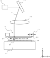
- FIG. 1 is a diagram illustrating a joining device in an embodiment of the present invention. It is a figure explaining the joint part in this embodiment.
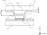
- FIG. 3 is a diagram illustrating a bonding form of elements by bonding according to the present embodiment. It is a figure explaining the junction form of the element in other embodiments of the present invention.
- a bonding device according to an embodiment of the present invention will be described with reference to FIG. 1.
- the bonding device 100 has an activation section 30 and a bonding section 10, and the bonding section 10 bonds elements whose bonding surfaces have been activated by the activation section 30.
- the element having the bonding surface may be in the form of a chip such as a semiconductor chip, or may be in the form of a substrate such as a circuit board.
- a plurality of chip-shaped elements are held in a plurality of arrays on a transfer substrate, and the elements are transported between the activation section 30 and the bonding section 10 in the form of a substrate, and are transported by a transport robot 40.
- the activation unit 30 is a plasma processing device, and has a chamber that accommodates a first element and a second element, and creates a plasma atmosphere in the chamber so as to improve the first bonding surface of the first element and the second element.
- the second bonding surface of the second element can be exposed to a plasma atmosphere.
- activation refers to bringing the surface of a substance into a state where a chemical reaction is likely to occur. Further, the process of activating the first bonding surface and the second bonding surface in this manner will be referred to as an activation step in this description.
- the transfer robot 40 moves the second element and the first element to the bonding area in this order. transported to.
- the first element is a semiconductor chip, and a plurality of them are arranged and held on the transfer substrate, and the second element is a circuit board.
- the transfer robot 40 has a substantially U-shaped robot hand and a movement mechanism for moving the robot hand, and has a surface opposite to the surface holding the first element of the transfer substrate, and a surface of the transfer substrate opposite to the surface holding the first element.
- the transfer substrate and the second element are transported from the activation section 30 to the bonding section 10 while holding the surface opposite to the bonding surface of the transfer substrate 2 by suction.
- the robot hand may have a reversing function.
- the second element is first conveyed to the bonding section 10, and then the transfer substrate is sucked and held, and the transfer substrate is transferred to the bonding section 10 while being reversed, so that the robot hand can move the transfer substrate to the bonding section 10 while holding the transfer substrate by suction.
- the first bonding surface and the second bonding surface may be opposed to each other.
- the joint portion 10 in this embodiment is shown in FIG. 2.
- the joining section 10 is a transfer device, and includes a laser irradiation section 12 that irradiates a laser beam 11, a transfer substrate gripping section 13 that holds the transfer substrate 22 and is movable in at least the X-axis direction and the Y-axis direction, and a transfer substrate gripping section.
- a transfer substrate holding section 14 is provided below the transfer substrate 13 and holds the transfer substrate 23 so as to face the transfer substrate 22 with a gap therebetween, and a control section (not shown) is provided.
- 11 causes ablation on the transfer substrate, and the element 21 is transferred from the transfer substrate 22 to the transferred substrate 23.
- the laser irradiation unit 12 is a device that irradiates laser light 11 such as an excimer laser that is an active energy ray, and is fixedly provided on the transfer device 10.
- the laser irradiation unit 12 irradiates a spot-shaped laser beam 11, and the laser beam 11 is transmitted in the X-axis direction and the Y-axis direction through a galvanometer mirror 15 and an f ⁇ lens 16 whose angle is adjusted by a control unit.
- the irradiation position in the direction is controlled, and a plurality of elements 21 arranged on the transfer substrate 22 held by the transfer substrate holding part 13 are selectively irradiated.
- the element 21 is a semiconductor chip such as a logic device or a memory, and will also be referred to as the chip 21 hereinafter. Furthermore, as shown in FIG. 3, one surface of the chip 21 is provided with a bonding surface 21a, which is a smooth surface on which wiring is formed to establish electrical continuity with the wiring board.
- the transfer substrate gripping section 13 has an opening and grips the vicinity of the outer circumference of the transfer substrate 22 by suction.
- the laser beam 11 emitted from the laser irradiation section 12 can be applied to the transfer substrate 22 held by the transfer substrate holding section 13 through this opening.
- the transfer robot hand that transfers the substrate S between the activation section 30 and the bonding section 10 may also serve as the transfer substrate gripping section 13.
- the transfer substrate 22 is a substrate made of glass or the like that can transmit the laser beam 11, and holds a plurality of chips 21 on the lower surface side. Further, as shown in FIG. 2(a), an adhesive layer 24 is formed on the surface of the transfer substrate 22 that holds the chip 21, and the surface of this adhesive layer 24 has adhesive properties. The adhesive force on the surface of the adhesive layer 24 serves as a holding force for the chip 21 and holds the chip 21 adhesively. Note that in this description, a substrate that holds an element (chip 21), such as the transfer substrate 22, is also referred to as a first holding substrate.
- the transfer substrate gripping section 13 is moved relative to the transferred substrate gripping section 14 in at least the X-axis direction and the Y-axis direction by a moving mechanism (not shown).
- a control section controls this moving mechanism and adjusts the position of the transfer substrate gripping section 13, thereby adjusting the relative position of the chip 1 held on the transfer substrate 22 with respect to the transfer target substrate 23.
- the transferred substrate holding part 14 has a flat surface on the upper surface, and during the transfer process of the chip 21, the adhesive layer 24 of the transfer substrate 22 and the transferred surfaces of the transferred substrate 23 and the adhesive layer 24 held by the adhesive layer 24 are held in a predetermined position.
- the transfer target substrate 23 is held so as to face each other with an interval of .
- a plurality of suction holes are provided on the upper surface of the transfer substrate gripping section 14, and the back surface (the surface to which the chip 1 is not transferred) of the transfer substrate 23 is gripped by suction force.
- the transfer target substrate 23 in this embodiment is a substrate to which a semiconductor chip is bonded, and is a circuit board provided with wiring for establishing electrical conduction with the chip 21, to which at least the chip 21 is bonded.
- the surface is provided with wiring and is a smooth surface.
- the transfer substrate gripping section 14 also has a moving mechanism in the X-axis direction and the Y-axis direction. It may be provided.
- the adhesive layer 24 is formed on the surface of the transfer substrate 22 that holds the chip 21.
- This adhesive layer 24 has adhesiveness on its surface, and blistering occurs within the adhesive layer 24 or between the glass surface 22a of the transfer substrate 22 and the adhesive layer 24 when irradiated with the laser beam 11. It has properties.
- the surface of the chip 21 opposite to the bonding surface is adhesively held on this adhesive layer 24 .
- the laser beam 11 is irradiated toward the chip 21 through the transfer substrate 22, and the chip 21 is adhesively held in the adhesive layer 24.
- the portion that is, the vicinity of the chip 21
- gas is generated.
- blisters (bubbles) 24a are generated inside the adhesive layer 24 or between the glass surface 22a of the transfer substrate 22 and the adhesive layer 24.
- the phenomenon in which the blisters 24a occur in this manner is referred to as blistering.
- a layer in which blistering occurs when energy is applied, such as the adhesive layer 24 of this embodiment is also referred to as a blistering layer in this description.
- the distance D2 of the surface of the adhesive layer 24 from the glass surface 22a in the portion where blistering has occurred in this manner is larger than the distance D1 of the surface of the adhesive layer 24 from the glass surface 22a in the portion before blistering. Therefore, when blistering occurs on the adhesive layer 24 at the position where the chip 21 is held, the chip 21 is separated from the glass surface 22a of the transfer substrate 22 while being held on the surface portion of the adhesive layer 24.
- the transfer substrate 23 is provided in the vicinity of the chip 21 so as to face it with a predetermined distance therebetween, the chip 21 is attached to the surface portion of the adhesive layer 24 due to the occurrence of blistering.
- the transfer target substrate 23 is approached while being held.
- the chip 21 will be moved to the transferred substrate 23 due to the occurrence of blistering. , and can be further pressed.
- proximity refers to the closeness of the target surfaces to such a distance that their electron trajectories overlap, and as the activated bonding surfaces come close to each other, the bonding surfaces become close to each other regardless of the presence or absence of external force. Joining begins.
- the bonding surface 21a of the chip 21 and the bonding surface 23a of the transfer substrate 23 are bonded by the bonding section 10 under the condition that the bonding surfaces of the chip 21 and the transfer target substrate 23 are activated in advance by the activation section 30. be able to.
- blistering is caused in the adhesive layer 24 and the chip 21 approaches the transfer substrate 23 while being held on the surface of the adhesive layer 24, so that for a predetermined period of time until the blister 24a deflates.
- the kinetic energy accompanying the blistering presses the chip 21 against the transfer target substrate 23, thereby promoting bonding between the activated bonding surfaces.
- the pressing force associated with this blistering is smaller than the pressing force due to ablation, which will be described later, and can press the chip 21 against the transfer substrate 23 weakly and for a long time compared to bonding by ablation.
- the bonding force between the chip 21 and the transfer substrate 23 when the blister 24a deflates is greater than the adhesion force of the chip 21 due to the adhesive layer 24, even if the blister 24a deflates, the chip 21 and the transfer substrate 23 will be bonded to each other. The joined state is maintained.
- the size of the blister 24a can be adjusted, and the pressing force of the chip 21 against the transfer target substrate 23 can be adjusted.
- the first bonding surface and the second bonding surface are brought close to each other by irradiation with active energy rays.
- the process of bonding by bonding is also referred to as a bonding step.
- the transfer substrate 23 can be bonded to the transfer substrate 23.
- the transfer substrate 22 and the transfer substrate 23 are separated by, for example, being raised by the operation of the transfer substrate gripping part 13, and the adhesive is removed from the chip 21. Layer 24 may also be removed.
- FIG. 4 shows a bonding form of elements in another embodiment of the present invention.
- blistering is caused in the adhesive layer 24 by irradiation with the laser beam 11 to bring the chip 21 close to the transfer target substrate 23, but in the bonding mode of this embodiment, the adhesive layer 24 The chip 21 is brought close to the transfer target substrate 23 by causing ablation.
- the laser beam 11 is irradiated toward the chip 21 through the transfer substrate 22, and the chip 21 is adhesively held in the ablation layer 24.
- the material of the adhesive layer 24 decomposes due to application of active energy (light energy), melts and disappears, and gas is generated. do. Due to the generation of gas as the adhesive layer 24 disappears, the chip 21 is peeled off from the transfer substrate 22 and is urged to move in a direction away from the transfer substrate 22. That is, laser lift-off is performed.
- ablation layer in this description.
- the transfer target substrate 23 is provided near the chip 21 so as to face it with a predetermined interval therebetween, so the chip 21 energized by the laser lift-off moves toward the transfer target substrate 23.
- the transfer target 23 flies close to the transfer target substrate 23. Then, under the condition that the bonding surfaces of the chip 21 and the transfer target substrate 23 are activated in advance by the activation unit 30, the bonding surface 21a of the adjacent chip 21 and the bonding surface 23a of the transfer target substrate 23 are the same as in the previous embodiment. Start joining in the same way.
- the chip 21 when the chip 21 approaches the transferred substrate 23, it is completely separated from the transfer substrate 22, so although it is difficult to obtain continuous pressing force during bonding, the chip 21 The chip 21 is momentarily pressed against the transfer target substrate 23 by the kinetic energy generated when it collides with the transfer target substrate 23, thereby promoting the bonding between the activated bonding surfaces.
- the bonding apparatus and bonding method of the present invention are not limited to the embodiments described above, but may have other embodiments within the scope of the present invention.
- the first element is pressed against the second element by kinetic energy accompanying blistering or ablation of the adhesive layer of the transfer substrate, and the bonding between the first bonding surface and the second bonding surface is promoted.
- the present invention is not limited to this, and a separate crimping process may be provided.
- the activation part and the joint part are separate devices, but the present invention is not limited thereto, and one device may serve as the activation part and the joint part. Then, with the transfer substrate gripping section gripping the back side of the transfer substrate and the transfer substrate gripping section gripping the back side of the transfer substrate, the bonding surface is activated by plasma or the like, and then the transfer substrate gripping section grips the back side of the transfer substrate.
- the chip may be transferred to the transfer substrate by irradiation with active energy rays while the transfer substrate gripping section holds the transfer substrate and the transfer substrate.
Landscapes
- Engineering & Computer Science (AREA)
- Mechanical Engineering (AREA)
- Die Bonding (AREA)
- Pressure Welding/Diffusion-Bonding (AREA)
- Manufacturing & Machinery (AREA)
- Wire Bonding (AREA)
Abstract
接合面の活性化をともなう接合を容易に実施することができる接合装置および接合方法を提供する。具体的には、第1の素子21と第2の素子23とを接合する接合装置100であって、第1の素子21の接合面である第1の接合面および第2の素子23の接合面である第2の接合面を活性化させる活性化部30と、第1の接合面と第2の接合面とを所定の間隔を介して対向させた状態から、活性エネルギー線の照射によって第1の接合面と第2の接合面とを近接させて接合させる接合部10と、を有する。
Description
本発明は、半導体チップと配線基板とを導通可能に接合する、接合装置および接合方法に関する。
材料同士を接合する技術の一つとして、ハイブリッドボンディングがある。ハイブリッドボンディングとは、電極パターンおよび絶縁層が同一面に混在した面間を接合する技術である。このとき、特許文献1に示されているように、接合する面同士がたとえばプラズマによって活性化した状態下で面同士を接触させることによって、両面の電子軌道が重なって接合が成立する。このように接合面を活性化させてから接合することにより、常温下で接合を実施することが可能であって熱変形が無視できるため、狭ピッチの電極パターンを有する材料の接合を行う場合にこの方法が適している。
しかし、上記の通り接合する面同士を活性化した状態下で接触させるためには、従来の接合装置では困難をともなっていた。具体的には、接合する材料が半導体チップと配線基板の場合、キャリア基板に多数配列された半導体チップの一部を配線基板に実装するにあたり、従来技術だとキャリア基板から対象の半導体チップをピックアップして、半導体チップの表裏面を持ち替えてから半導体チップを配線基板に向けて搬送することにより、両者の接合面を対向させる。一方、両者の接合面を活性化させている場合には、半導体チップの接合面側を保持する際には、その接合面が搬送ハンドと接触してはいけないため、搬送ハンドはベルヌーイチャックなど特殊なものを使用する必要があった。また、チップをキャリア基板から外す際にキャリア基板側からチップをニードルで突く場合、チップが割れる可能性もあった。
本願発明は、上記問題点を鑑み、接合面の活性化をともなう接合を容易に実施することができる接合装置および接合方法を提供することを目的とする。
上記課題を解決するために本発明の接合装置は、第1の素子と第2の素子とを接合する接合装置であって、前記第1の素子の接合面である第1の接合面および前記第2の素子の接合面である第2の接合面を活性化させる活性化部と、前記第1の接合面と前記第2の接合面とを所定の間隔を介して対向させた状態から、活性エネルギー線の照射によって前記第1の接合面と前記第2の接合面とを近接させて接合させる接合部と、を有することを特徴としている。
この接合装置により、接合部では活性エネルギー線の照射によって第1の接合面と第2の接合面とを近接させるため、第1の素子の集合の中から任意の第1の素子を一度取り外して搬送する工程が不要となる。そのため、第1の素子の第1の接合面に物理的な接触が途中で生じることなく第1の素子を第2の素子へ近接させることができるため、接合面が活性化された状態を壊すことなく第1の素子と第2の素子とを接合させることができる。
また、前記第1の素子を保持する第1の保持基板には活性エネルギー線の照射によりブリスタリングが生じるブリスタリング層が設けられ、前記ブリスタリングにより前記第1の素子が前記ブリスタリング層に保持された状態で前記第2の素子に近接すると良い。
こうすることにより、確実に第1の素子を第2の素子に近接させることができる。
また、前記第1の素子を保持する第1の保持基板には活性エネルギー線の照射によりアブレーションが生じる粘着層が設けられ、前記アブレーションにより前記第1の素子が付勢されつつ前記第1の保持基板から剥離し、前記第2の素子に近接しても良い。
こうすることにより、確実に第1の素子を第2の素子に近接させることができる。
また、前記接合部は、活性エネルギー線の照射により前記第1の接合面と前記第2の接合面とを近接させるとともに所定の圧力で前記第1の接合面と前記第2の接合面とを押圧させると良い。
こうすることにより、第1の接合面と第2の接合面の接合を促進させることができる。
また、前記活性化部は、前記第1の接合面および前記第2の接合面をプラズマ雰囲気に曝すことにより、それぞれを活性化させると良い。
また、上記課題を解決するために本発明の接合方法は、第1の素子と第2の素子とを接合する接合方法であって、前記第1の素子の接合面である第1の接合面および前記第2の素子の接合面である第2の接合面を活性化させる活性化工程と、前記第1の接合面と前記第2の接合面とを所定の間隔を介して対向させた状態から、活性エネルギー線の照射によって前記第1の接合面と前記第2の接合面とを近接させて接合させる接合工程と、を有することを特徴としている。
この接合方法により、接合工程では活性エネルギー線の照射によって第1の接合面と第2の接合面とを近接させるため、第1の素子の集合の中から任意の第1の素子を一度取り外して搬送する工程が不要となる。そのため、第1の素子の第1の接合面に物理的な接触が途中で生じることなく第1の素子を第2の素子へ近接させることができるため、接合面が活性化された状態を壊すことなく第1の素子と第2の素子とを接合させることができる。
本発明の接合装置および接合方法により、接合面の活性化をともなう接合を容易に実施することができる。
本発明の一実施形態における接合装置について、図1を参照して説明する。
接合装置100は活性化部30および接合部10を有し、活性化部30により接合面が活性化された素子同士を接合部10で接合する。ここで、接合面を有する素子は、半導体チップのようなチップ状でも良く、回路基板のような基板状でも良い。チップ状の素子は、転写基板に複数配列するように保持されており、活性化部30と接合部10の間の素子の搬送は、基板の形態で行われ、搬送ロボット40により搬送される。
活性化部30は、プラズマ処理装置であり、第1の素子および第2の素子を収容するチャンバを有し、チャンバ内をプラズマ雰囲気にすることにより第1の素子が有する第1の接合面および第2の素子が有する第2の接合面をプラズマ雰囲気に曝すことができる。このように第1の接合面および第2の接合面をプラズマ雰囲気に曝すことにより、それぞれを活性化させる。なお、活性化とは、物質の表面を化学反応が起こりやすい状態にすることを指す。また、このように第1の接合面および第2の接合面を活性化させるプロセスを、本説明では活性化工程と呼ぶ。
活性化部30による第1の素子の第1の接合面および第2の素子の第2の接合面の活性化が完了すると、第2の素子、第1の素子の順に搬送ロボット40によって接合部へと搬送される。ここで、本実施形態では、後述する通り、第1の素子は半導体チップであって転写基板に複数個配列されて保持された状態であり、第2の素子は回路基板であるとする。
搬送ロボット40は、略U字状のロボットハンドと当該ロボットハンドを移動させる移動機構を有し、転写基板の第1の素子を保持している面と反対側の面、第2の素子の第2の接合面と反対側の面をそれぞれ吸着保持し、転写基板および第2の素子を活性化部30から接合部10へ搬送する。
また、ロボットハンドは反転機能を有していても良い。この場合、第2の素子を先に接合部10へ搬送させてから転写基板を吸着保持し、反転しながら接合部10へ搬送することによって、ロボットハンドが転写基板を吸着保持したまま接合部10内で第1の接合面と第2の接合面とが対向する形態をとっても良い。
本実施形態における接合部10を図2に示す。
接合部10は、転写装置であり、レーザ光11を照射するレーザ照射部12、転写基板22を保持して少なくともX軸方向、Y軸方向に移動可能な転写基板把持部13、転写基板把持部13の下側にあって転写基板22と隙間を有して対向するように被転写基板23を保持する被転写基板把持部14、および図示しない制御部を備えており、転写基板22にレーザ光11を照射することによって転写基板でアブレーションを生じさせ、転写基板22から被転写基板23へ素子21を転写する。
なお、接合部10では素子の接合面が活性化された状態を維持する必要があるため、装置内に減圧された環境が形成されていることが好ましい。
レーザ照射部12は、活性エネルギー線であるエキシマレーザなどのレーザ光11を照射する装置であり、転写装置10に固定して設けられる。本実施形態においては、レーザ照射部12はスポット状のレーザ光11を照射し、レーザ光11は、制御部により角度が調節されるガルバノミラー15およびfθレンズ16を介してX軸方向およびY軸方向の照射位置が制御され、転写基板把持部13に保持された転写基板22に複数配置されている素子21に選択的に照射する。レーザ光11が転写基板22を通して素子21近傍に入射することによって、転写基板22と素子21との間で活性エネルギー(光エネルギー)の付与によるブリスタリングが生じ、このブリスタリングによって素子21は被転写基板23へ向かって移動し、素子21と被転写基板23の接合面同士が近接する。
なお、本説明では素子21はロジックデバイスやメモリなどの半導体チップであり、以降、チップ21とも呼ぶ。また、チップ21の一方の面には、図3に示すように配線基板との導通を得るための配線が形成された平滑面である接合面21aが設けられている。
転写基板把持部13は開口を有し、転写基板22の外周部近傍を吸着把持する。転写基板把持部13に保持された転写基板22へこの開口を介してレーザ照射部12から発せられたレーザ光11を当てることができる。なお、上記の通り活性化部30と接合部10の間で基板Sを搬送する搬送ロボットハンドが、この転写基板把持部13を兼ねても良い。
転写基板22は、ガラスなどを材料としてレーザ光11を透過することが可能な基板であり、下面側で複数のチップ21を保持する。また、この転写基板22のチップ21を保持する面には図2(a)に示すように粘着層24が形成されており、この粘着層24の表面は粘着性を有する。この粘着層24の表面の粘着力がチップ21の保持力となり、チップ21を粘着保持する。なお、本説明では転写基板22のように素子(チップ21)を保持する基板を第1の保持基板とも呼ぶ。
また、転写基板把持部13は図示しない移動機構により、少なくともX軸方向、Y軸方向に関して被転写基板把持部14に対して相対移動する。図示しない制御部がこの移動機構を制御し、転写基板把持部13の位置を調節することにより、転写基板22に保持されたチップ1の被転写基板23に対する相対位置を調節することができる。
被転写基板把持部14は、上面に平坦面を有し、チップ21の転写工程中、転写基板22の粘着層24および粘着層24が保持するチップ21と被転写基板23の被転写面が所定の間隔を介して対向するように被転写基板23を把持する。この被転写基板把持部14の上面には複数の吸引孔が設けられており、吸引力により被転写基板23の裏面(チップ1が転写されない方の面)を把持する。
ここで、本実施形態における被転写基板23は、半導体チップが接合される基板であり、チップ21との導通をとるための配線が設けられた回路基板であって、少なくともチップ21が接合される面は配線が設けられ、かつ平滑面となっている。
なお、本実施形態では、転写基板把持部13のみがX軸方向およびY軸方向に移動することにより転写基板把持部13と被転写基板把持部14とが相対移動する形態をとっているが、被転写基板23の寸法が大きく、レーザ光11の照射範囲の直下に被転写基板23の全面が位置できない場合には、被転写基板把持部14にもX軸方向およびY軸方向の移動機構が設けられていても良い。
本実施形態の転写装置10による本発明にかかるチップ21の接合形態を図3で説明する。
転写基板22のチップ21を保持する面には、上述の通り粘着層24が形成されている。この粘着層24は、表面に粘着性を有しているとともに、レーザ光11が照射されることにより粘着層24内もしくは転写基板22のガラス面22aと粘着層24との間でブリスタリングが生じる性質を有している。この粘着層24に、チップ21は接合面と反対側の面が粘着保持されている。
ここで、チップ21を挟んで転写基板22と被転写基板23とが対向した状態において転写基板22を通してチップ21に向けてレーザ光11が照射され、粘着層24におけるチップ21を粘着保持している部分(すなわち、チップ21の近傍)にレーザ光11が照射されることによって、レーザ光11のエネルギーによって粘着層24の材料の一部が分解され、ガスが発生する。この粘着層24の材料の分解およびガスの発生により、粘着層24の内部もしくは転写基板22のガラス面22aと粘着層24との間でブリスター(気泡)24aが発生する。このようにブリスター24aが発生する現象を本説明ではブリスタリングと呼ぶ。また、本実施形態の粘着層24のようにエネルギーの付与によりブリスタリングが生じる層を、本説明ではブリスタリング層とも呼ぶ。
このようにブリスタリングが生じた部分における粘着層24の表面のガラス面22aからの距離D2は、ブリスタリングする前の部分における粘着層24の表面のガラス面22aからの距離D1より大きくなる。そのため、チップ21が保持されている位置において粘着層24にブリスタリングが生じると、チップ21は粘着層24の表面部分に保持されたまま転写基板22のガラス面22aから離間する。
ここで、本実施形態では、チップ21の近傍には所定の間隔を介して対向するように被転写基板23が設けられているため、ブリスタリングの発生によりチップ21は粘着層24の表面部分に保持されたまま被転写基板23に接近する。
そして、ブリスタリング前におけるチップ21と被転写基板23との距離がブリスタリングの発生により生じうる粘着層24の表面の位置変動量よりも小さければ、ブリスタリングの発生によってチップ21は被転写基板23に近接し、さらに押圧されうる。
なお、本説明における近接とは、対象面同士が電子軌道を重ねる程度の距離まで接近することを指し、活性化された接合面同士が近接することにより、外力の有無に関係無く接合面同士の接合が開始する。
したがって、活性化部30によってあらかじめチップ21と被転写基板23の接合面同士が活性化された条件下において接合部10によってチップ21の接合面21aと被転写基板23の接合面23aとを接合させることができる。
また、本実施形態では粘着層24にてブリスタリングを生じさせてチップ21が粘着層24の表面部分に保持されたまま被転写基板23に近接するため、ブリスター24aがしぼむまでの所定の時間においてブリスタリングにともなう運動エネルギーによってチップ21を被転写基板23へ押圧し、それにより、活性化された接合面同士の接合を促進させることができる。
また、このブリスタリングにともなう押圧力は、後述のアブレーションによる押圧力より小さく、アブレーションによる接合と比較してチップ21を被転写基板23へ弱く長く押圧することができる。
そして、ブリスター24aがしぼむ際のチップ21と被転写基板23との接合力が粘着層24によるチップ21の粘着力よりも大きくなっていれば、ブリスター24aがしぼんでもチップ21と被転写基板23とが接合された状態は維持される。
また、レーザ光11の強度を調節することによりブリスター24aの大きさを調節することが可能であり、チップ21の被転写基板23への押圧力を調節することができる。
また、上記の通り第1の接合面と第2の接合面とを所定の間隔を介して対向させた状態から、活性エネルギー線の照射によって第1の接合面と第2の接合面とを近接させて接合させるプロセスを、本説明では接合工程とも呼ぶ。
このような接合工程により、チップの集合の中から任意のチップ21を一度取り外して搬送する工程を要することなく被転写基板23へ近接させることができる。そのため、チップ21の接合面21aに物理的な接触が途中で生じることなくチップ21を被転写基板23へ近接させることができるため、接合面が活性化された状態を壊すことなくチップ21と被転写基板23とを接合させることができる。
なお、チップ21と被転写基板23とが接合された後、たとえば転写基板把持部13の動作により転写基板22を上昇させることによって転写基板22と被転写基板23とを離間させ、チップ21から粘着層24を取り外すようにしても良い。
次に、本発明の他の実施形態における素子の接合形態を図4に示す。
先述の実施形態の接合形態では、レーザ光11の照射により粘着層24においてブリスタリングを発生させてチップ21を被転写基板23に近接させているが、本実施形態の接合形態では、粘着層24でアブレーションを生じさせることによりチップ21を被転写基板23に近接させる。
具体的には、チップ21を挟んで転写基板22と被転写基板23とが対向した状態において転写基板22を通してチップ21に向けてレーザ光11が照射され、アブレーション層24におけるチップ21を粘着保持している部分(すなわち、チップ21の近傍)にレーザ光11が照射されることによって、活性エネルギー(光エネルギー)の付与による粘着層24の材料の分解が生じ、溶融、消失するとともに、ガスが発生する。この粘着層24の消失にともなうガスの発生により、チップ21は転写基板22から剥離するとともに付勢され、転写基板22から離れる方向へ移動する。すなわち、レーザリフトオフが実施される。
なお、本実施形態の粘着層24のようにエネルギーの付与によりアブレーションが生じる層を、本説明ではアブレーション層とも呼ぶ。
ここで、本実施形態ではチップ21の近傍には所定の間隔を介して対向するように被転写基板23が設けられているため、レーザリフトオフにより付勢されたチップ21は被転写基板23に向かって飛行し、被転写基板23に近接する。そして、活性化部30によってあらかじめチップ21と被転写基板23の接合面同士が活性化された条件下において、近接したチップ21の接合面21aと被転写基板23の接合面23aは先の実施形態と同様に接合を開始する。
また、本実施形態ではチップ21が被転写基板23に近接する際には転写基板22から完全に分離しているため、接合の際に継続的な押圧力を得ることは難しいものの、チップ21が被転写基板23に衝突した際の運動エネルギーによってチップ21を被転写基板23へ瞬間的に押圧し、それにより、活性化された接合面同士の接合を促進させることができる。
以上の接合装置および接合方法により、接合面の活性化をともなう接合を容易に実施することが可能である。
ここで、本発明の接合装置および接合方法は、以上で説明した形態に限らず本発明の範囲内において他の形態のものであってもよい。たとえば、上記の説明では転写基板の粘着層のブリスタリングもしくはアブレーションにともなう運動エネルギーにより第1の素子を第2の素子に押圧し、第1の接合面と第2の接合面の接合を促進しているが、それに限らず別途圧着工程を設けても良い。
また、上記の説明では、活性化部と接合部とが別々の装置となっているが、それに限らず、一つの装置が活性化部と接合部を兼ねても良い。そして、転写基板把持部が転写基板の裏面側を把持し、被転写基板把持部が被転写基板の裏面側を把持した状態でプラズマなどによる接合面の活性化を行い、次に転写基板把持部および被転写基板把持部が転写基板および被転写基板を把持した状態を維持したまま活性エネルギー線照射による被転写基板へのチップの転写を行っても良い。
10 接合部(転写装置)
11 レーザ光(活性エネルギー線)
12 レーザ光源
13 転写基板把持部
14 被転写基板把持部
15 ガルバノミラー
16 Fθレンズ
21 チップ(素子)
21a 接合面
22 転写基板
22a ガラス面
23 被転写基板(回路基板)
23a 接合面
24 粘着層
24a ブリスター
30 活性化部
40 ロボットハンド
100 接合装置
S 基板
11 レーザ光(活性エネルギー線)
12 レーザ光源
13 転写基板把持部
14 被転写基板把持部
15 ガルバノミラー
16 Fθレンズ
21 チップ(素子)
21a 接合面
22 転写基板
22a ガラス面
23 被転写基板(回路基板)
23a 接合面
24 粘着層
24a ブリスター
30 活性化部
40 ロボットハンド
100 接合装置
S 基板
Claims (6)
- 第1の素子と第2の素子とを接合する接合装置であって、
前記第1の素子の接合面である第1の接合面および前記第2の素子の接合面である第2の接合面を活性化させる活性化部と、
前記第1の接合面と前記第2の接合面とを所定の間隔を介して対向させた状態から、活性エネルギー線の照射によって前記第1の接合面と前記第2の接合面とを近接させて接合させる接合部と、
を有することを特徴とする、接合装置。 - 前記第1の素子を保持する第1の保持基板には活性エネルギー線の照射によりブリスタリングが生じるブリスタリング層が設けられ、前記ブリスタリングにより前記第1の素子が前記ブリスタリング層に保持された状態で前記第2の素子に近接することを特徴とする、請求項1に記載の接合装置。
- 前記第1の素子を保持する第1の保持基板には活性エネルギー線の照射によりアブレーションが生じる粘着層が設けられ、前記アブレーションにより前記第1の素子が付勢されつつ前記第1の保持基板から剥離し、前記第2の素子に近接することを特徴とする、請求項1に記載の接合装置。
- 前記接合部は、活性エネルギー線の照射により前記第1の接合面と前記第2の接合面とを近接させるとともに所定の圧力で前記第1の接合面と前記第2の接合面とを押圧させることを特徴とする、請求項1から3のいずれかに記載の接合装置。
- 前記活性化部は、前記第1の接合面および前記第2の接合面をプラズマ雰囲気に曝すことにより、それぞれを活性化させることを特徴とする、請求項1から4のいずれかに記載の接合装置。
- 第1の素子と第2の素子とを接合する接合方法であって、
前記第1の素子の接合面である第1の接合面および前記第2の素子の接合面である第2の接合面を活性化させる活性化工程と、
前記第1の接合面と前記第2の接合面とを所定の間隔を介して対向させた状態から、活性エネルギー線の照射によって前記第1の接合面と前記第2の接合面とを近接させて接合させる接合工程と、
を有することを特徴とする、接合方法。
Priority Applications (2)
| Application Number | Priority Date | Filing Date | Title |
|---|---|---|---|
| KR1020247030199A KR20240167641A (ko) | 2022-03-28 | 2023-03-27 | 접합 장치 및 접합 방법 |
| US18/892,975 US20250015039A1 (en) | 2022-03-28 | 2024-09-23 | Bonding device and bonding method |
Applications Claiming Priority (2)
| Application Number | Priority Date | Filing Date | Title |
|---|---|---|---|
| JP2022-051064 | 2022-03-28 | ||
| JP2022051064A JP2023144203A (ja) | 2022-03-28 | 2022-03-28 | 接合装置および接合方法 |
Related Child Applications (1)
| Application Number | Title | Priority Date | Filing Date |
|---|---|---|---|
| US18/892,975 Continuation US20250015039A1 (en) | 2022-03-28 | 2024-09-23 | Bonding device and bonding method |
Publications (1)
| Publication Number | Publication Date |
|---|---|
| WO2023190384A1 true WO2023190384A1 (ja) | 2023-10-05 |
Family
ID=88202300
Family Applications (1)
| Application Number | Title | Priority Date | Filing Date |
|---|---|---|---|
| PCT/JP2023/012288 Ceased WO2023190384A1 (ja) | 2022-03-28 | 2023-03-27 | 接合装置および接合方法 |
Country Status (5)
| Country | Link |
|---|---|
| US (1) | US20250015039A1 (ja) |
| JP (1) | JP2023144203A (ja) |
| KR (1) | KR20240167641A (ja) |
| TW (1) | TW202406655A (ja) |
| WO (1) | WO2023190384A1 (ja) |
Cited By (1)
| Publication number | Priority date | Publication date | Assignee | Title |
|---|---|---|---|---|
| WO2025204883A1 (ja) * | 2024-03-26 | 2025-10-02 | 東レエンジニアリング株式会社 | デバイス製造システムおよびデバイス製造方法 |
Citations (3)
| Publication number | Priority date | Publication date | Assignee | Title |
|---|---|---|---|---|
| JP2019503081A (ja) * | 2016-01-15 | 2019-01-31 | ユニカルタ・インコーポレイテッド | 超小型又は超薄型ディスクリート部品の配置 |
| JP2019527465A (ja) * | 2017-06-12 | 2019-09-26 | ユニカルタ・インコーポレイテッド | 基板上に個別部品を並列に組み立てる方法 |
| US20210375620A1 (en) * | 2020-06-02 | 2021-12-02 | Intel Corporation | Iii-n multichip modules and methods of fabrication |
Family Cites Families (1)
| Publication number | Priority date | Publication date | Assignee | Title |
|---|---|---|---|---|
| JPS6448656U (ja) | 1987-09-18 | 1989-03-27 |
-
2022
- 2022-03-28 JP JP2022051064A patent/JP2023144203A/ja active Pending
-
2023
- 2023-03-27 KR KR1020247030199A patent/KR20240167641A/ko active Pending
- 2023-03-27 WO PCT/JP2023/012288 patent/WO2023190384A1/ja not_active Ceased
- 2023-03-28 TW TW112111716A patent/TW202406655A/zh unknown
-
2024
- 2024-09-23 US US18/892,975 patent/US20250015039A1/en active Pending
Patent Citations (3)
| Publication number | Priority date | Publication date | Assignee | Title |
|---|---|---|---|---|
| JP2019503081A (ja) * | 2016-01-15 | 2019-01-31 | ユニカルタ・インコーポレイテッド | 超小型又は超薄型ディスクリート部品の配置 |
| JP2019527465A (ja) * | 2017-06-12 | 2019-09-26 | ユニカルタ・インコーポレイテッド | 基板上に個別部品を並列に組み立てる方法 |
| US20210375620A1 (en) * | 2020-06-02 | 2021-12-02 | Intel Corporation | Iii-n multichip modules and methods of fabrication |
Cited By (1)
| Publication number | Priority date | Publication date | Assignee | Title |
|---|---|---|---|---|
| WO2025204883A1 (ja) * | 2024-03-26 | 2025-10-02 | 東レエンジニアリング株式会社 | デバイス製造システムおよびデバイス製造方法 |
Also Published As
| Publication number | Publication date |
|---|---|
| TW202406655A (zh) | 2024-02-16 |
| JP2023144203A (ja) | 2023-10-11 |
| KR20240167641A (ko) | 2024-11-27 |
| US20250015039A1 (en) | 2025-01-09 |
Similar Documents
| Publication | Publication Date | Title |
|---|---|---|
| CN112166495A (zh) | 工件分离装置及工件分离方法 | |
| CN103962728A (zh) | 激光加工方法 | |
| WO2023190384A1 (ja) | 接合装置および接合方法 | |
| TW202409718A (zh) | 轉印裝置及轉印方法 | |
| CN108346597B (zh) | 一种真空加热系统、晶片剥离装置及方法 | |
| WO2023190389A1 (ja) | 転写装置および転写方法 | |
| JP7503886B2 (ja) | ウェーハの加工方法 | |
| TW202105487A (zh) | 晶圓的加工方法 | |
| JP4114196B2 (ja) | 電子部品の剥離方法及びその実装方法 | |
| JP2016058542A (ja) | チップと基板との接合方法、チップと基板との仮接合装置、チップ実装システム | |
| JP7824210B2 (ja) | 転写装置 | |
| JP2020064989A (ja) | ウェーハの加工方法 | |
| JP2025148673A (ja) | 転写方法、及び転写装置 | |
| TWI876690B (zh) | 晶片接合設備以及晶片接合方法 | |
| TW201936307A (zh) | 輪對輪的滾動焊接設備 | |
| JP2024099423A (ja) | 転写方法 | |
| CN120089608A (zh) | 芯片接合设备以及芯片接合方法 | |
| WO2024122552A1 (ja) | 転写方法 | |
| JP2020064986A (ja) | ウェーハの加工方法 | |
| JP2020077706A (ja) | ウェーハの加工方法 | |
| JP5667320B1 (ja) | 部材貼付け装置 | |
| JP2020064988A (ja) | ウェーハの加工方法 | |
| KR20210004848A (ko) | 광 디바이스의 이설 방법 | |
| JP2020064959A (ja) | ウェーハの加工方法 | |
| JPH01149978A (ja) | 薄膜の加工方法 |
Legal Events
| Date | Code | Title | Description |
|---|---|---|---|
| 121 | Ep: the epo has been informed by wipo that ep was designated in this application |
Ref document number: 23780393 Country of ref document: EP Kind code of ref document: A1 |
|
| NENP | Non-entry into the national phase |
Ref country code: DE |
|
| 122 | Ep: pct application non-entry in european phase |
Ref document number: 23780393 Country of ref document: EP Kind code of ref document: A1 |