WO2023190336A1 - Light-emitting element, and method and device for manufacturing same - Google Patents
Light-emitting element, and method and device for manufacturing same Download PDFInfo
- Publication number
- WO2023190336A1 WO2023190336A1 PCT/JP2023/012194 JP2023012194W WO2023190336A1 WO 2023190336 A1 WO2023190336 A1 WO 2023190336A1 JP 2023012194 W JP2023012194 W JP 2023012194W WO 2023190336 A1 WO2023190336 A1 WO 2023190336A1
- Authority
- WO
- WIPO (PCT)
- Prior art keywords
- type semiconductor
- light emitting
- substrate
- active
- semiconductor portion
- Prior art date
Links
- 238000000034 method Methods 0.000 title claims description 96
- 238000004519 manufacturing process Methods 0.000 title claims description 72
- 239000004065 semiconductor Substances 0.000 claims abstract description 605
- 239000000463 material Substances 0.000 claims abstract description 156
- 239000000758 substrate Substances 0.000 claims description 261
- 239000013078 crystal Substances 0.000 claims description 38
- 150000004767 nitrides Chemical class 0.000 claims description 24
- 230000003287 optical effect Effects 0.000 claims description 22
- 239000004020 conductor Substances 0.000 claims description 5
- 238000000016 photochemical curing Methods 0.000 claims description 3
- 229920001187 thermosetting polymer Polymers 0.000 claims description 3
- 239000010408 film Substances 0.000 description 169
- 239000010410 layer Substances 0.000 description 47
- JMASRVWKEDWRBT-UHFFFAOYSA-N Gallium nitride Chemical compound [Ga]#N JMASRVWKEDWRBT-UHFFFAOYSA-N 0.000 description 36
- 229910002601 GaN Inorganic materials 0.000 description 34
- 238000005530 etching Methods 0.000 description 22
- 230000015572 biosynthetic process Effects 0.000 description 19
- 238000003776 cleavage reaction Methods 0.000 description 16
- 230000007017 scission Effects 0.000 description 16
- VYPSYNLAJGMNEJ-UHFFFAOYSA-N Silicium dioxide Chemical compound O=[Si]=O VYPSYNLAJGMNEJ-UHFFFAOYSA-N 0.000 description 11
- 238000005253 cladding Methods 0.000 description 11
- 230000007547 defect Effects 0.000 description 11
- 229910052814 silicon oxide Inorganic materials 0.000 description 11
- 238000001312 dry etching Methods 0.000 description 10
- KRHYYFGTRYWZRS-UHFFFAOYSA-N Fluorane Chemical compound F KRHYYFGTRYWZRS-UHFFFAOYSA-N 0.000 description 9
- 230000006870 function Effects 0.000 description 9
- HBMJWWWQQXIZIP-UHFFFAOYSA-N silicon carbide Chemical compound [Si+]#[C-] HBMJWWWQQXIZIP-UHFFFAOYSA-N 0.000 description 9
- 229910010271 silicon carbide Inorganic materials 0.000 description 9
- 229910052581 Si3N4 Inorganic materials 0.000 description 8
- HQVNEWCFYHHQES-UHFFFAOYSA-N silicon nitride Chemical compound N12[Si]34N5[Si]62N3[Si]51N64 HQVNEWCFYHHQES-UHFFFAOYSA-N 0.000 description 8
- 238000004544 sputter deposition Methods 0.000 description 8
- 229910000679 solder Inorganic materials 0.000 description 7
- PMHQVHHXPFUNSP-UHFFFAOYSA-M copper(1+);methylsulfanylmethane;bromide Chemical compound Br[Cu].CSC PMHQVHHXPFUNSP-UHFFFAOYSA-M 0.000 description 6
- 230000000694 effects Effects 0.000 description 6
- 239000002994 raw material Substances 0.000 description 6
- 229910052710 silicon Inorganic materials 0.000 description 6
- 238000012546 transfer Methods 0.000 description 6
- 229910002704 AlGaN Inorganic materials 0.000 description 5
- XUIMIQQOPSSXEZ-UHFFFAOYSA-N Silicon Chemical compound [Si] XUIMIQQOPSSXEZ-UHFFFAOYSA-N 0.000 description 5
- 230000000903 blocking effect Effects 0.000 description 5
- 238000005229 chemical vapour deposition Methods 0.000 description 5
- 230000008569 process Effects 0.000 description 5
- 239000010703 silicon Substances 0.000 description 5
- 230000008901 benefit Effects 0.000 description 4
- 230000007423 decrease Effects 0.000 description 4
- 238000010586 diagram Methods 0.000 description 4
- 238000000206 photolithography Methods 0.000 description 4
- 239000002356 single layer Substances 0.000 description 4
- 239000010936 titanium Substances 0.000 description 4
- 229910052782 aluminium Inorganic materials 0.000 description 3
- 230000010355 oscillation Effects 0.000 description 3
- 238000012545 processing Methods 0.000 description 3
- 229910052594 sapphire Inorganic materials 0.000 description 3
- 239000010980 sapphire Substances 0.000 description 3
- 238000011144 upstream manufacturing Methods 0.000 description 3
- NWAIGJYBQQYSPW-UHFFFAOYSA-N azanylidyneindigane Chemical compound [In]#N NWAIGJYBQQYSPW-UHFFFAOYSA-N 0.000 description 2
- 230000008859 change Effects 0.000 description 2
- 238000004140 cleaning Methods 0.000 description 2
- 238000000313 electron-beam-induced deposition Methods 0.000 description 2
- 238000007429 general method Methods 0.000 description 2
- 230000017525 heat dissipation Effects 0.000 description 2
- 239000011159 matrix material Substances 0.000 description 2
- 238000005259 measurement Methods 0.000 description 2
- 238000002844 melting Methods 0.000 description 2
- 230000008018 melting Effects 0.000 description 2
- 229910052751 metal Inorganic materials 0.000 description 2
- 239000002184 metal Substances 0.000 description 2
- 238000012986 modification Methods 0.000 description 2
- 230000004048 modification Effects 0.000 description 2
- TWNQGVIAIRXVLR-UHFFFAOYSA-N oxo(oxoalumanyloxy)alumane Chemical compound O=[Al]O[Al]=O TWNQGVIAIRXVLR-UHFFFAOYSA-N 0.000 description 2
- 238000001020 plasma etching Methods 0.000 description 2
- 229910052718 tin Inorganic materials 0.000 description 2
- 229910052719 titanium Inorganic materials 0.000 description 2
- XCZXGTMEAKBVPV-UHFFFAOYSA-N trimethylgallium Chemical compound C[Ga](C)C XCZXGTMEAKBVPV-UHFFFAOYSA-N 0.000 description 2
- 229910052582 BN Inorganic materials 0.000 description 1
- PZNSFCLAULLKQX-UHFFFAOYSA-N Boron nitride Chemical compound N#B PZNSFCLAULLKQX-UHFFFAOYSA-N 0.000 description 1
- GYHNNYVSQQEPJS-UHFFFAOYSA-N Gallium Chemical group [Ga] GYHNNYVSQQEPJS-UHFFFAOYSA-N 0.000 description 1
- 206010053759 Growth retardation Diseases 0.000 description 1
- 208000012868 Overgrowth Diseases 0.000 description 1
- 229910004205 SiNX Inorganic materials 0.000 description 1
- 229910004298 SiO 2 Inorganic materials 0.000 description 1
- ATJFFYVFTNAWJD-UHFFFAOYSA-N Tin Chemical compound [Sn] ATJFFYVFTNAWJD-UHFFFAOYSA-N 0.000 description 1
- GWEVSGVZZGPLCZ-UHFFFAOYSA-N Titan oxide Chemical compound O=[Ti]=O GWEVSGVZZGPLCZ-UHFFFAOYSA-N 0.000 description 1
- NRTOMJZYCJJWKI-UHFFFAOYSA-N Titanium nitride Chemical compound [Ti]#N NRTOMJZYCJJWKI-UHFFFAOYSA-N 0.000 description 1
- YAIQCYZCSGLAAN-UHFFFAOYSA-N [Si+4].[O-2].[Al+3] Chemical compound [Si+4].[O-2].[Al+3] YAIQCYZCSGLAAN-UHFFFAOYSA-N 0.000 description 1
- 230000002159 abnormal effect Effects 0.000 description 1
- 230000009471 action Effects 0.000 description 1
- AUCDRFABNLOFRE-UHFFFAOYSA-N alumane;indium Chemical compound [AlH3].[In] AUCDRFABNLOFRE-UHFFFAOYSA-N 0.000 description 1
- XAGFODPZIPBFFR-UHFFFAOYSA-N aluminium Chemical compound [Al] XAGFODPZIPBFFR-UHFFFAOYSA-N 0.000 description 1
- 229910052804 chromium Inorganic materials 0.000 description 1
- 239000011248 coating agent Substances 0.000 description 1
- 238000000576 coating method Methods 0.000 description 1
- 238000004891 communication Methods 0.000 description 1
- 239000000470 constituent Substances 0.000 description 1
- 238000001816 cooling Methods 0.000 description 1
- 238000005520 cutting process Methods 0.000 description 1
- 238000000151 deposition Methods 0.000 description 1
- 230000008021 deposition Effects 0.000 description 1
- 229910003460 diamond Inorganic materials 0.000 description 1
- 239000010432 diamond Substances 0.000 description 1
- 238000005516 engineering process Methods 0.000 description 1
- 239000012530 fluid Substances 0.000 description 1
- 238000009499 grossing Methods 0.000 description 1
- 230000012447 hatching Effects 0.000 description 1
- 238000010438 heat treatment Methods 0.000 description 1
- 229910052738 indium Inorganic materials 0.000 description 1
- 150000002500 ions Chemical group 0.000 description 1
- 238000005304 joining Methods 0.000 description 1
- 238000010030 laminating Methods 0.000 description 1
- 238000004020 luminiscence type Methods 0.000 description 1
- 239000012528 membrane Substances 0.000 description 1
- 229910021421 monocrystalline silicon Inorganic materials 0.000 description 1
- QPJSUIGXIBEQAC-UHFFFAOYSA-N n-(2,4-dichloro-5-propan-2-yloxyphenyl)acetamide Chemical compound CC(C)OC1=CC(NC(C)=O)=C(Cl)C=C1Cl QPJSUIGXIBEQAC-UHFFFAOYSA-N 0.000 description 1
- 229910052759 nickel Inorganic materials 0.000 description 1
- 229910052758 niobium Inorganic materials 0.000 description 1
- 125000004433 nitrogen atom Chemical group N* 0.000 description 1
- 239000012811 non-conductive material Substances 0.000 description 1
- BPUBBGLMJRNUCC-UHFFFAOYSA-N oxygen(2-);tantalum(5+) Chemical compound [O-2].[O-2].[O-2].[O-2].[O-2].[Ta+5].[Ta+5] BPUBBGLMJRNUCC-UHFFFAOYSA-N 0.000 description 1
- RVTZCBVAJQQJTK-UHFFFAOYSA-N oxygen(2-);zirconium(4+) Chemical compound [O-2].[O-2].[Zr+4] RVTZCBVAJQQJTK-UHFFFAOYSA-N 0.000 description 1
- 229910052763 palladium Inorganic materials 0.000 description 1
- 238000002161 passivation Methods 0.000 description 1
- 238000000623 plasma-assisted chemical vapour deposition Methods 0.000 description 1
- 229910052697 platinum Inorganic materials 0.000 description 1
- 238000005498 polishing Methods 0.000 description 1
- 238000007639 printing Methods 0.000 description 1
- 230000006798 recombination Effects 0.000 description 1
- 238000005215 recombination Methods 0.000 description 1
- 230000009467 reduction Effects 0.000 description 1
- 230000002040 relaxant effect Effects 0.000 description 1
- 229910052703 rhodium Inorganic materials 0.000 description 1
- 239000011265 semifinished product Substances 0.000 description 1
- 238000000926 separation method Methods 0.000 description 1
- 229910001936 tantalum oxide Inorganic materials 0.000 description 1
- 239000010409 thin film Substances 0.000 description 1
- OGIDPMRJRNCKJF-UHFFFAOYSA-N titanium oxide Inorganic materials [Ti]=O OGIDPMRJRNCKJF-UHFFFAOYSA-N 0.000 description 1
- 238000011282 treatment Methods 0.000 description 1
- 238000007740 vapor deposition Methods 0.000 description 1
- 229910052725 zinc Inorganic materials 0.000 description 1
- 229910052984 zinc sulfide Inorganic materials 0.000 description 1
- 229910052726 zirconium Inorganic materials 0.000 description 1
- 229910001928 zirconium oxide Inorganic materials 0.000 description 1
Images


Classifications
-
- H—ELECTRICITY
- H01—ELECTRIC ELEMENTS
- H01L—SEMICONDUCTOR DEVICES NOT COVERED BY CLASS H10
- H01L33/00—Semiconductor devices with at least one potential-jump barrier or surface barrier specially adapted for light emission; Processes or apparatus specially adapted for the manufacture or treatment thereof or of parts thereof; Details thereof
- H01L33/48—Semiconductor devices with at least one potential-jump barrier or surface barrier specially adapted for light emission; Processes or apparatus specially adapted for the manufacture or treatment thereof or of parts thereof; Details thereof characterised by the semiconductor body packages
- H01L33/62—Arrangements for conducting electric current to or from the semiconductor body, e.g. lead-frames, wire-bonds or solder balls
-
- H—ELECTRICITY
- H01—ELECTRIC ELEMENTS
- H01S—DEVICES USING THE PROCESS OF LIGHT AMPLIFICATION BY STIMULATED EMISSION OF RADIATION [LASER] TO AMPLIFY OR GENERATE LIGHT; DEVICES USING STIMULATED EMISSION OF ELECTROMAGNETIC RADIATION IN WAVE RANGES OTHER THAN OPTICAL
- H01S5/00—Semiconductor lasers
- H01S5/02—Structural details or components not essential to laser action
- H01S5/022—Mountings; Housings
- H01S5/0235—Method for mounting laser chips
- H01S5/02355—Fixing laser chips on mounts
- H01S5/0237—Fixing laser chips on mounts by soldering
-
- H—ELECTRICITY
- H01—ELECTRIC ELEMENTS
- H01S—DEVICES USING THE PROCESS OF LIGHT AMPLIFICATION BY STIMULATED EMISSION OF RADIATION [LASER] TO AMPLIFY OR GENERATE LIGHT; DEVICES USING STIMULATED EMISSION OF ELECTROMAGNETIC RADIATION IN WAVE RANGES OTHER THAN OPTICAL
- H01S5/00—Semiconductor lasers
- H01S5/20—Structure or shape of the semiconductor body to guide the optical wave ; Confining structures perpendicular to the optical axis, e.g. index or gain guiding, stripe geometry, broad area lasers, gain tailoring, transverse or lateral reflectors, special cladding structures, MQW barrier reflection layers
- H01S5/22—Structure or shape of the semiconductor body to guide the optical wave ; Confining structures perpendicular to the optical axis, e.g. index or gain guiding, stripe geometry, broad area lasers, gain tailoring, transverse or lateral reflectors, special cladding structures, MQW barrier reflection layers having a ridge or stripe structure
Definitions
- the present disclosure relates to light emitting devices and the like.
- light emitting elements such as light emitting diodes are sometimes manufactured by mounting individualized light emitting bodies (sometimes referred to as dies) on a support such as a substrate.
- a support such as a substrate.
- an electrode on the surface side of a light emitting body formed by laminating semiconductor layers on a growth substrate and an electrode on a support are bonded via a conductive bonding material such as solder (so-called flip-chip bonding).
- a mounting method is known (see Patent Document 1). Such a mounting method is also called "junction down mounting.”
- a light emitting element includes a first type semiconductor portion having a first type conductivity and a first side surface, an active portion located below the first type semiconductor portion, and a second type conductivity.
- a second type semiconductor part having a conductive bonding material and a second type semiconductor part disposed from below the active part to a side of the first type semiconductor part; a support body located below and supporting the light emitting body via the conductive bonding material so that the first type semiconductor part is located above the active part.
- a method for manufacturing a light emitting element includes the steps of: preparing a semiconductor substrate in which a first type semiconductor portion having a first side surface is formed on a base substrate; a step of forming an active part; a step of forming a second type semiconductor part disposed from above the active part to a side of the first type semiconductor part; a step of preparing a support substrate; A light emitting body including at least a portion of each of the first type semiconductor part, the active part, and the second type semiconductor part is connected to a conductive junction such that the first type semiconductor part is located above the active part. and a step of bonding to the support substrate via a material.
- a method for manufacturing a light emitting device includes the steps of: preparing a semiconductor substrate in which a first type semiconductor portion, an active portion, and a second type semiconductor portion are formed in this order on a base substrate; a step of forming an insulating film on at least one side surface of the type semiconductor section, the active section, and the second type semiconductor section; a step of preparing a supporting substrate; bonding a light emitting body including at least a portion of each type 2 semiconductor part to the supporting substrate via a conductive bonding material such that the first type semiconductor part is located above the active part; include.
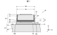
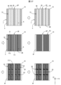
- FIG. 1 is a cross-sectional view schematically showing the configuration of a light emitting element in an embodiment of the present disclosure.
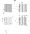
- FIG. 2 is a perspective view schematically illustrating an example of a process of junction-down mounting a light emitting body on a support body.
- FIG. 2 is a cross-sectional view illustrating an example of a method for manufacturing a light emitting element in an embodiment of the present disclosure.
- 1 is a plan view schematically showing an example of a method for manufacturing a light emitting element in an embodiment of the present disclosure.
- 1 is a flowchart illustrating an example of a method for manufacturing a light emitting element in an embodiment of the present disclosure.
- FIG. 7 is a cross-sectional view showing a light emitting element in another configuration example of an embodiment of the present disclosure.
- FIG. 7 is a cross-sectional view showing a light emitting element in another configuration example of an embodiment of the present disclosure.
- FIG. 7 is a cross-sectional view showing a light emitting element in another configuration example of an embodiment of the present disclosure.
- 2 is a perspective view showing the configuration of a light emitting body in Example 1.
- FIG. FIG. 2 is a perspective view showing the configuration of an optical resonator.
- FIG. 3 is a plan view showing the configuration of an active part.
- FIG. 3 is a plan view showing the configuration of an active part.
- FIG. 3 is a cross-sectional view showing the configuration of a light emitter in Example 1.
- FIG. 1 is a flowchart schematically showing a method for manufacturing a light emitting device in Example 1.
- FIG. 1 is a plan view schematically showing a method for manufacturing a light emitter included in a light emitting element in Example 1.
- FIG. 1 is a cross-sectional view schematically showing a method for manufacturing a light emitting device in Example 1.
- FIG. 1 is a cross-sectional view schematically showing a method for manufacturing a light emitting device in Example 1.
- FIG. 1 is a cross-sectional view schematically showing a method for manufacturing a light emitting device in Example 1.
- FIG. FIG. 2 is a cross-sectional view showing a configuration example of a template substrate.
- FIG. 3 is a plan view showing an example of the configuration of a support substrate.
- FIG. 1 is a flowchart schematically showing a method for manufacturing a light emitting device in Example 1.
- FIG. 2 is a perspective view schematically showing a light-emitting substrate in which a plurality of light-emitting bodies are bonded to a support substrate.
- FIG. 2 is a perspective view showing an example of a bar-shaped light emitting substrate after being divided.
- 1 is a perspective view showing the configuration of a light emitting element in Example 1.
- FIG. 1 is a cross-sectional view showing the configuration of a light emitting element in Example 1.
- FIG. 3 is a perspective view showing the configuration of a light emitting element in another example of Example 1.
- FIG. 3 is a cross-sectional view showing the configuration of a light emitting element in another example of Example 1.
- FIG. FIG. 3 is a cross-sectional view schematically showing a method for manufacturing a light emitting device in another example of Example 1.
- FIG. 7 is a flowchart schematically showing a method for manufacturing a light emitting device in Example 2.
- FIG. 3 is a cross-sectional view schematically showing a method for manufacturing a light emitting device in Example 2.
- FIG. 3 is a plan view schematically showing a method for manufacturing a light emitting element in Example 2.
- FIG. 7 is a plan view schematically showing a method for manufacturing a light emitting element in another example of Example 2.
- FIG. FIG. 3 is a cross-sectional view showing an example of lateral growth of a base semiconductor portion.
- FIG. 7 is a cross-sectional view schematically showing a method for manufacturing a light emitting device in Example 3.
- 7 is a flowchart schematically showing a method for manufacturing a light emitting element in Example 4.
- FIG. 4 is a flowchart schematically showing a method for manufacturing a light emitting element in Example 4.
- FIG. 7 is a cross-sectional view schematically showing a method for manufacturing a light emitting element in Example 4.
- FIG. 7 is a cross-sectional view schematically showing a method for manufacturing a light emitting element in Example 4.
- FIG. 7 is a perspective view showing the configuration of a light emitting body in Example 5.
- FIG. 7 is a partial cross-sectional view of a light emitter in Example 5.
- FIG. 7 is a partial plan view of a light emitter in Example 5.
- FIG. 7 is a plan view schematically showing a method for manufacturing a light emitting element in Example 5.
- 7 is a plan view schematically showing a method for manufacturing a light emitting element in another example of Example 5.
- FIG. FIG. 7 is a plan view schematically showing a method for manufacturing a light emitting element in Example 6.
- FIG. 1 is a cross-sectional view schematically showing the configuration of a light emitting element in an embodiment of the present disclosure.
- the light-emitting element 30 in this embodiment includes a light-emitting body 20, a bonding material having conductivity (conductive bonding material) CA, and a support that supports the light-emitting body 20 via the bonding material CA.
- ST for example, submount
- the light emitting body 20 includes (i) a first type semiconductor portion S1 having a first side surface FS and having first type conductivity; (ii) an active portion AP located below the first type semiconductor portion S1; (iii) a second type semiconductor part S2 having second type conductivity and arranged from below the active part AP to the side of the first type semiconductor part S1;
- the direction from the light emitter 20 to the support ST is defined as the downward direction (negative side in the Z1 axis direction).
- the support body ST is located below the light emitter 20 and supports the light emitter 20 via the bonding material CA so that the first type semiconductor portion S1 is located above the active portion AP.
- the first type semiconductor portion S1 may be a first type semiconductor layer
- the second type semiconductor portion S2 may be a second type semiconductor layer
- the active portion AP may be an active layer.
- the light emitter 20 may be, for example, a semiconductor laser diode (an edge-emitting type or a surface-emitting type laser diode), or a light emitting diode.
- the first type semiconductor portion S1 may have n-type conductivity
- the second type semiconductor portion S2 may have p-type conductivity.
- the present invention is not limited to this, and the first type semiconductor portion S1 may have p-type conductivity, and the second type semiconductor portion S2 may have n-type conductivity.
- the first type semiconductor portion S1 and the second type semiconductor portion S2 may include a nitride semiconductor (for example, a GaN-based semiconductor).
- a GaN-based semiconductor is a semiconductor containing gallium atoms (Ga) and nitrogen atoms (N), and typical examples include GaN, AlGaN, AlGaInN, and InGaN.
- the first type semiconductor portion S1 may include a non-doped (i-type) semiconductor portion.
- the first type semiconductor section S1 may include a doped semiconductor section.
- a portion of the first type semiconductor portion S1 in contact with the active portion AP may be an n-type semiconductor portion containing a donor.
- the second type semiconductor portion S2 may include a non-doped (i-type) semiconductor portion.
- a portion of the second type semiconductor portion S2 that is in contact with the active portion AP may be a non-doped (i-type) semiconductor portion.
- the direction in which the first type semiconductor part S1, the active part AP, and the second type semiconductor part S2 of the light emitting body 20 are stacked between the first type semiconductor part S1 and the support ST is defined as the Z1 axis direction.
- the thickness of the first type semiconductor portion S1 in the Z1 axis direction is greater than the thickness of the second type semiconductor portion S2 in the Z1 axis direction.
- the first type semiconductor portion S1 may include a substrate for crystal growth, and in this case, the thickness of the first type semiconductor portion S1 in the Z1 axis direction is greater than the thickness of the second type semiconductor portion S2 in the Z1 axis direction. is also significantly larger.
- the light-emitting body 20 (die) having a double-sided electrode structure is junction-down mounted (face-down mounted) on the support ST (mounting substrate, etc.).
- Junction-down mounting is a format in which the light emitting body 20 is mounted on the support ST so that the active part AP is located between the support ST and the first type semiconductor section S1.
- junction-down mounting has the advantage of improving heat dissipation. This is because the active part AP, which is considered to be a heat generating part, can be brought closer to the support ST which also functions as a heat radiating member.
- the light emitter 20 may have a first electrode E1 located below the second type semiconductor portion S2 and a second electrode E2 located above the first type semiconductor portion S1.
- the support ST may include a base portion BP, and a first pad portion P1 and a second pad portion P2 located above the base portion BP.
- the base portion BP may be the main body portion (for example, a substrate) of the support ST.
- the first pad portion P1 and the first electrode E1 may be electrically connected to each other via the bonding material CA.
- the second pad portion P2 and the second electrode E2 may be electrically connected to each other by a wire, a conductive film, or the like (not shown).
- the first side surface FS of the first type semiconductor section S1 may be one of two side surfaces facing each other in the width direction (X-axis direction) of the first type semiconductor section S1.
- the width direction (X-axis direction) of the first type semiconductor portion S1 may be the a-axis direction of the nitride semiconductor crystal.
- the first side surface FS may be the side surface farthest from the second pad portion P2 of the two side surfaces facing each other in the X-axis direction in the first type semiconductor portion S1.
- the second type semiconductor portion S2 may be thinner than the first type semiconductor portion S1. At least a portion of the second type semiconductor portion S2 may be in contact with the first side surface FS.
- the bonding material CA may have fluidity and may flow upstream along the second type semiconductor portion S2 located on the side of the first side surface FS.
- the light emitting element 30 is not limited to the example shown in FIG. 1, and the bonding material CA does not need to run up along the second type semiconductor portion S2.
- EP1 The end of the bonding material CA flowing up along the second type semiconductor portion S2 on the positive side in the Z1 axis direction (the side far from the support ST) is referred to as EP1.
- EP2 the end point on the first side surface FS side of the lower (negative side in the Z1-axis direction) surface of the second type semiconductor portion S2 is referred to as EP2.
- the position of the end EP2 in the Z1 axis direction the position of the end EP1 above the end EP2 is referred to as the run-up height H1 of the bonding material CA.
- the run-up height H1 may exceed the lower surface level LV of the first type semiconductor portion S1.
- the lower surface level LV corresponds to the position of the boundary between the first type semiconductor portion S1 and the active portion AP in the Z1-axis direction.
- Planar view Viewing the light emitting element 30 along the Z1 axis direction corresponding to the stacking direction of the first type semiconductor section S1 and the active section AP can be called a "planar view".
- two ends of the bonding material CA in the width direction (X-axis direction) of the light emitting body 20 are defined as an edge ED1 and an edge ED2, respectively.
- the edge ED1 is the end of the bonding material CA on the first side surface FS side.
- at least a portion of the edge ED1 and the edge ED2 may protrude from the light-emitting body 20 in plan view.
- the width W2 of the bonding material CA which is the distance between the edge ED1 and the edge ED2 in the X-axis direction, may be larger than the width W1 of the light-emitting body 20 in the X-axis direction.
- the light emitting device 30 in this embodiment will be described in more detail as follows, along with a general explanation of the findings of the present disclosure.
- an edge-emitting laser diode (hereinafter referred to as a laser element), which is a type of light emitting element, may be formed as follows. First, various semiconductor layers are stacked on a growth substrate (for example, a substrate containing an n-type semiconductor), and a ridge structure, electrodes, etc. are formed. As a result, a laser wafer having a device structure is manufactured. Then, for example, after polishing the growth substrate to make it thin, the laser wafer is cleaved (primary cleavage) to form elongated rectangular parallelepiped-shaped laser bars.
- a growth substrate for example, a substrate containing an n-type semiconductor
- a ridge structure, electrodes, etc. are formed as a result.
- a laser wafer having a device structure is manufactured. Then, for example, after polishing the growth substrate to make it thin, the laser wafer is cleaved (primary cleavage) to form elongated rectangular parallelepiped
- the laser bar is cleaved (secondary cleavage) to be divided. This forms a laser body (light-emitting body). Thereafter, the laser body is mounted on a submount to manufacture a laser element.
- junction-up mounting since the thickness of the first type semiconductor portion S1 is relatively thick, it is relatively difficult for a pn short circuit to occur even if the bonding material CA runs up. However, such a measure cannot be applied in a case where junction-down mounting is assumed as in the case of the light emitting element 30 in this embodiment.
- FIG. 2 is a perspective view schematically illustrating an example of a process for junction-down mounting a light emitter on a support.
- FIG. 3 is a cross-sectional view showing an example of a method for manufacturing a light emitting element in this embodiment.
- the structure of the light emitting body 20 is shown in a simplified manner for clarity of illustration, and the bonding material CA is hatched.
- the bonding material CA is placed on the first pad portion P1 corresponding to the position on the support ST where the light emitting body 20 is mounted.
- the support body ST may be a part of a support substrate SK (see FIG. 17 etc.) which will be described later.
- the bonding material CA may be made of a conductive material having at least one of heat fluidity, pressure curability, thermosetting property, and photocuring property.
- the bonding material CA placed on the first pad portion P1 has a certain thickness (height in the Z1 axis direction).
- the thickness of the bonding material CA may be greater than the thickness of the second type semiconductor portion S2.
- the thickness of the bonding material CA may be approximately 5 ⁇ m, and the thickness of the second type semiconductor portion S2 may be approximately 0.5 ⁇ m.
- the bonding material CA has greater wettability with the first pad portion P1 than with the base portion BP.
- the width W1 of the light emitter 20 may be, for example, 120 ⁇ m or less, 100 ⁇ m or less, 80 ⁇ m or less, or 60 ⁇ m or less. Although the lower limit of the width W1 of the light emitter 20 is not particularly limited, the width W1 may be, for example, 40 ⁇ m or more.
- the width W3 of the bonding material CA may be, for example, 10 ⁇ m or more from the viewpoint of reducing the possibility of bonding failure.
- the width W3 of the bonding material CA may be smaller than the width W1, may be equal to the width W1, or may be larger than the width W1.
- the light emitter 20 Before joining the light emitter 20 to the support ST, the light emitter 20 may be held, for example, by a general holding means (such as a collet), or may be held by a growth substrate (for example, (see Figure 3).
- a general holding means such as a collet
- a growth substrate for example, (see Figure 3).
- Two side faces of the light emitter 20 facing each other in the X-axis direction are referred to as side faces 20T1 and 20T2
- an end face of the light emitter 20 in the Y-axis direction is referred to as an end face 20F.
- the side surfaces 20T1 and 20T2 may be collectively referred to as the side surface 20T.
- the bonding material CA can run up along the side surface 20T of the light-emitting body 20.
- the bonding material CA can go upstream along the side surface 20T1
- the bonding material CA can also go upstream along the side surface 20T2.
- the second type semiconductor portion S2 exists between the bonding material CA that has gone up and the first type semiconductor portion S1 (first side surface FS thereof) (see FIG. 1). Therefore, the possibility that the first electrode E1 and the first type semiconductor portion S1 will be short-circuited via the bonding material CA can be effectively reduced.
- the light emitting body 20 is, for example, a semiconductor laser diode
- a resonator end face is formed on the end face 20F and is not covered by the second type semiconductor portion S2.
- the light-emitting body 20 may be junction-down mounted on the support ST such that the end surface 20F protrudes (protrudes) from the first pad portion P1 in the Y-axis direction. Since the first pad portion P1 is thin, illustration of the end surface of the first pad portion P1 is omitted in FIG. 2.
- the light emitting element 30 may have a distance L10 from the end surface of the first pad portion P1 to the end surface 20F of the light emitting body 20 in the Y-axis direction, and in this case, the bonding material CA runs up along the end surface 20F. Possibility can be reduced.
- the side surface 20T2 that is closer to the second pad portion P2 (the negative side in the X-axis direction) is in a position that protrudes from the first pad portion P1 in the X-axis direction. It's okay. In this case, the possibility that the bonding material CA runs up along the side surface 20T2 can be reduced. On the other hand, the bonding material CA can go up along the side surface 20T1.
- the bonding material CA may have fluidity and may typically be solder.
- the bonding material CA may be, for example, a solder pump, or a thin solder film formed by printing, vapor deposition, or sputtering.
- the semiconductor substrate 10 may include a main substrate 1, a base portion 4, and a plurality of light emitters 20, as will be described in detail in Examples described later.
- at least a portion of the first type semiconductor portion S1 included in the light emitter 20 may be formed by an ELO (Epitaxial Lateral Overgrowth) method.
- the distance from the boundary between the light emitter 20 and the base portion 4 to the surface of the first electrode E1 on the support substrate SK side is defined as the height H2 of each light emitter 20.
- the plurality of light emitters 20 may have slightly different heights H2. Since the bonding material CA has fluidity, even if the heights H2 differ, it is possible to easily transfer two or more light emitters 20 at once to the support substrate SK while being separated from the base substrate BK. . After the light emitter 20 is transferred to the support substrate SK, the base portion BP may be divided. Thereby, it is possible to form a light emitting element 30 in which at least one light emitting body 20 is junction-down mounted on the support ST.
- the bonding material CA has fluidity, when the light emitter 20 and the support substrate SK are brought close to each other and a load is applied, the controllability of the range in which the bonding material CA exists may deteriorate.
- the width W1 of the light emitter 20 is small, the bonding material CA tends to run up the side surface 20T of the light emitter 20. If the width W3 of the bonding material CA is narrowed, the transfer yield may decrease due to a decrease in bonding force and a requirement for higher mounting accuracy (alignment).
- the bonding material CA moves up the side surface 20T of the light emitting body 20, the bonding material CA that has gone up and the (first side surface FS of) the first type semiconductor part S1 A second type semiconductor portion S2 exists between them (see FIG. 1). Therefore, while ensuring the size of the width W3 of the bonding material CA, it is possible to effectively reduce the possibility that the first electrode E1 and the first type semiconductor portion S1 will be short-circuited via the bonding material CA.
- the bonding material CA runs up the side surface 20T of the light emitting body 20 (wrapping around the side surface 20T), so that it also has the following advantages. That is, the bonding force between the support substrate SK and the light emitting body 20 via the bonding material CA can be improved, and the light emitting body 20 can be suppressed by the bonding material CA.
- the bonding material CA comes into contact with a part of the side surface 20T and forms a shape that at least partially holds (holds) the light emitter 20, the bonding strength between the support substrate SK and the light emitter 20 is improved.
- the bonding material CA and the light emitting body 20 are difficult to separate, and therefore it becomes easy to separate the light emitting body 20 from the base substrate BK. Moreover, the heat dissipation of the light emitter 20 can be easily improved.
- the run-up height H1 of the bonding material CA exceeds the lower surface level LV of the first type semiconductor portion S1, the above-mentioned effect becomes even more remarkable.
- FIG. 4 is a plan view schematically showing an example of a method for manufacturing a light emitting element in this embodiment.
- FIG. 5 is a flowchart illustrating an example of a method for manufacturing a light emitting element in this embodiment.
- the light emitting body 20 may be a laser body having a double-sided electrode structure. Other methods of manufacturing various light emitters 20 will be described later as examples.
- each member in the plan view is given the same hatching as each member in the cross-sectional view shown in FIG. 1, etc.
- the method for manufacturing the light emitting device 30 includes a step of preparing a semiconductor substrate 10 in which a first type semiconductor portion S1 having a first side surface FS is formed on a base substrate BK. and forming an active part AP above the first type semiconductor part S1, and forming a second type semiconductor part S2 arranged from above the active part AP to the side of the first type semiconductor part S1. and a step of doing so.
- layers such as the first type semiconductor portion S1 are stacked on the base substrate BK, and the stacking direction is defined as an upward direction (positive side in the Z2 axis direction).
- the direction of the Z2 axis may be reversed with respect to the Z1 axis described in FIG. 1 and the like described above.
- the semiconductor substrate 10 is upside down with respect to the support substrate SK.
- one XYZ axis and two XYZ axes may be used depending on the subject of the description.
- the semiconductor substrate 10 is inverted with the X axis as the rotation axis, and the junction is attached to the support substrate SK. It will be mounted down, and the X-axis and Y-axis will be used in common.
- the semiconductor substrate 10 may have a plurality of bar-shaped first type semiconductor portions S1 arranged side by side in the X-axis direction.
- the first type semiconductor portion S1 may have a longitudinal shape whose longitudinal direction is in the Y-axis direction.
- the first type semiconductor part S1 may include a lateral growth part formed by the ELO method and a vertical growth part (regrowth part) formed by general epitaxial growth above the lateral growth part. good.
- the semiconductor substrate 10 may have a gap GP between adjacent first type semiconductor parts S1.
- the second type semiconductor part S2 can be formed so as to cover at least a part of the first side surface FS.
- the gap GP is a space formed by stopping lateral growth before adjacent crystals grown by the ELO method meet each other when at least a portion of the first type semiconductor portion S1 is formed by the ELO method. It may be. Alternatively, the gap GP may be a trench formed by etching the first type semiconductor portion S1 formed in a plate shape. Further, the base substrate BK may be a growth substrate used to form the first type semiconductor section S1. The base substrate BK only needs to be such that the light emitters 20 can be separated from each other when the light emitters 20 are transferred to the support substrate SK.
- the base substrate BK may include a Si substrate or a SiC substrate and a seed layer (for example, a GaN-based semiconductor), or the base substrate BK may include a GaN-based free-standing substrate (single-crystal substrate). There may be.
- the first type semiconductor section S1 may have a first side surface FS, which is one of two side surfaces facing each other in the X-axis direction, and a second side surface SS, which is the other side.
- the first side surface FS and the second side surface SS are side surfaces when the first type semiconductor portion S1 is formed, and may be formed of a crystal plane of a nitride semiconductor.
- a surface naturally generated by crystal growth may be referred to as a "crystal surface”
- a surface formed by processing such as etching may be referred to as a "processed surface”.
- the planes produced by the cleavage of the crystal are called "cleavage planes.”
- the second type semiconductor part S2 is arranged from above the active part AP to the side of the first side surface FS in the first type semiconductor part S1, and from above the active part AP to the first side surface FS. It may be arranged so as to extend to the side of the second side surface SS in the type semiconductor portion S1.
- a ridge portion (not shown) may be formed in the second type semiconductor portion S2, and the first electrode E1 may be formed so as to overlap the ridge portion in plan view.
- two members overlap means that at least a portion of one member overlaps another member in a plan view (including a perspective plan view) in the thickness direction of each member. These members may or may not be in contact with each other.
- the first electrode E1 may have a contact electrode and an auxiliary electrode (sometimes referred to as a pad electrode).
- a plurality of first electrodes E1 arranged in the Y-axis direction may be formed above the second type semiconductor portion S2.
- a plurality of open groove portions GS are formed in the elongated stacked body LB including the first type semiconductor portion S1, the active portion AP, the second type semiconductor portion S2, and the first electrode E1. Thereby, the stacked body LB is divided into a plurality of light emitters 20.
- the open groove portion GS may be a gap space formed by cleaving the stacked body LB, or may be a gap space formed by etching the stacked body LB.
- the method for manufacturing the light emitting element 30 according to the present embodiment further includes a step of preparing a support substrate SK, and a light emitting body including at least a portion of each of the first type semiconductor part S1, the active part AP, and the second type semiconductor part S2. 20 to the support substrate SK via a bonding material (conductive bonding material) CA such that the first type semiconductor portion S1 is located above the active portion AP.
- a bonding material conductive bonding material
- the light emitter 20 has a double-sided electrode structure
- a first type semiconductor portion is placed on the surface of the light emitter 20 opposite to the side on which the first electrode E1 is provided.
- a second electrode E2 electrically connected to S1 can be formed. Thereafter, the second electrode E2 and the second pad portion P2 can be electrically connected using a conductive film or the like.
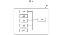
- FIG. 6 is a block diagram showing an example of a light emitting device manufacturing apparatus in this embodiment.
- the manufacturing apparatus 40 in FIG. 6 includes an apparatus 40A for preparing the semiconductor substrate 10, an apparatus 40B for forming the active part AP, an apparatus 40C for forming the second type semiconductor part S2, an apparatus 40D for preparing the support substrate SK, and a light emitting body 20. It may have a device 40E for bonding the device to the support substrate SK, and a device 40F for controlling the devices 40A to 40E. Further, the manufacturing apparatus 40 may appropriately include devices for executing various specific steps described in the examples described later.
- an MOCVD (Metal-Organic Chemical Vapor Deposition) device can be used as the device 40B and the device 40C.
- a sputtering device or a photolithography device may be used as appropriate.
- Device 40F may include a processor and memory.
- the device 40F may be configured to control the devices 40A to 40E by executing a program stored in, for example, a built-in memory, a communicable communication device, or an accessible network.
- the manufacturing apparatus 40 When using the semiconductor substrate 10 prepared in advance, the manufacturing apparatus 40 does not need to include the apparatus 40A. When using the support substrate SK prepared in advance, the manufacturing apparatus 40 does not need to include the apparatus 40D.
- FIG. 7A is a cross-sectional view showing a light emitting element in another configuration example of an embodiment of the present disclosure.
- the active part AP may be arranged from below the first type semiconductor part S1 to the side of the first type semiconductor part S1.
- the active part AP extends from below the first type semiconductor part S1 to the side of the first side surface FS of the first type semiconductor part S1 and to the side of the second side surface SS. They may be arranged so as to reach each other. Since the film thickness of the active area AP is very thin, the thickness of the active area AP is exaggerated in FIG. 7A.
- FIG. 7B is a cross-sectional view showing a light emitting element 30 in another configuration example of an embodiment of the present disclosure.
- a ridge portion RJ may be formed in the second type semiconductor portion S2.
- the ridge portion RJ may be located at a position overlapping the first electrode E1 in a plan view, and the first electrode E1 may include a first contact electrode E11 and a first auxiliary electrode E12.
- an insulating film DF may be provided on both sides of the ridge portion RJ, and the insulating film DF extends from below the second type semiconductor portion S2 excluding the ridge portion RJ to the side of the first type semiconductor portion S1. It may be arranged as follows.
- the insulating film DF extends from below the second type semiconductor portion S2 excluding the ridge portion RJ to the side of the first side surface FS in the first type semiconductor portion S1, and extends to the side of the second side surface SS. It may be arranged so as to extend to the side.
- the insulating film DF located on both sides of the ridge portion RJ and the insulating film DF located on the side of the first type semiconductor portion S1 may be formed integrally (continuously) with each other, or may be formed separately. It's okay.
- the insulating film DF first insulating film located on the side of the first type semiconductor portion S1 ( A second insulating film) may also be formed.
- the second type semiconductor portion S2 may exist between the first side surface FS and the insulating film DF, or the second type semiconductor portion S2 may not exist.
- the insulating film DF is formed between the first side surface FS and the bonding material CA. exists. Thereby, the possibility that the first electrode E1 and the first type semiconductor portion S1 will be short-circuited via the bonding material CA can be effectively reduced.
- the light-emitting element 30 may have a configuration in which the light-emitting body 20 is, for example, a light-emitting diode, and does not have the ridge portion RJ in the example shown in FIG. 7B.
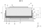
- FIG. 7C is a cross-sectional view showing a light emitting element 30 in another configuration example of an embodiment of the present disclosure.
- the second type semiconductor portion S2 may be disposed so as to extend from below the active portion AP to the side of the first type semiconductor portion S1. It may be located over the entire surface (see FIG. 1), or may be located so as to cover a part of the first side surface FS. That is, the first side surface FS may have a portion on the side where the second type semiconductor portion S2 is not located, and for example, a part of the first side surface FS may be exposed.
- the height in the Z1-axis direction of the second-type semiconductor portion S2 located on the side of the first-type semiconductor portion S1 is referred to as a formation height H3.
- the upper end in the Z1-axis direction of the second-type semiconductor part S2 located on the side of the first-type semiconductor part S1 is referred to as EP3, and the formation height H3 is equal to the height H3 of the second-type semiconductor part S2 in the Z1-axis direction. This is the height position of the end portion EP3 above the end portion EP2 with reference to the position of the lower end portion EP2.
- the second type semiconductor portion S2 extends from below the active portion AP to the side of the first type semiconductor portion S1. That is, the second type semiconductor portion S2 is located below the active portion AP and on at least a portion of the side of the first side surface FS. The second type semiconductor portion S2 may be continuous from below the active portion AP to the end portion EP3.
- the formation height H3 may be smaller than the sum T1 of the thicknesses of the first type semiconductor portion S1, the active portion AP, and the second type semiconductor portion S2 in the Z1 axis direction.
- the reaching position of the wrap-around portion of the second type semiconductor portion S2 (the position of the end portion EP3) is higher than the run-up position of the bonding material CA (the position of the end portion EP1).
- the position of the end portion EP3 may be above the center of the first side surface FS, may be one height above.
- the formation height H3 of the second type semiconductor portion S2 is larger than the run-up height H1 of the bonding material CA, so that the first electrode E1 and the first type semiconductor portion S1 are connected to each other through the bonding material CA. This can effectively reduce the possibility of short circuits.
- the light emitting element 30 may have the first side surface FS covered with an insulating film DF (see FIG. 7B).
- the light emitting element 30 may have the same configuration (arrangement relationship of each part) on the second side surface SS as described above for the first side surface FS.
- Example 1 an example will be described in which the light emitting body 20 is a laser body (semiconductor laser chip) having a single-sided two-electrode structure, and the light emitting element 30 is a laser element.
- the light emitting body 20 is a laser body (semiconductor laser chip) having a single-sided two-electrode structure
- the light emitting element 30 is a laser element.
- the configuration of the light emitting body 20 will be explained, and then the light emitting element 30 will be explained together with the explanation of its manufacturing method.
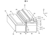
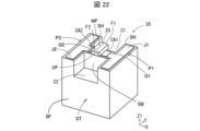
- FIG. 8 is a perspective view showing the configuration of a light emitting body in Example 1.
- FIG. 9 is a perspective view showing the configuration of an optical resonator.
- FIGS. 10A and 10B are plan views showing the configuration of the active part.
- FIG. 11 is a cross-sectional view showing the configuration of the light emitter in Example 1.
- the light emitting body 20 in Example 1 includes a first type semiconductor part S1, an active part AP located above the first type semiconductor part S1, and a first type semiconductor part S1 from above the active part AP. It may include a second type semiconductor part S2 arranged so as to extend to the side of the type semiconductor part S1. The second type semiconductor portion S2 may cover at least a portion of the first side surface FS of the first type semiconductor portion S1.
- the first type semiconductor portion S1, the active portion AP, and the second type semiconductor portion S2 may each contain a nitride semiconductor (for example, a GaN-based semiconductor).
- a nitride semiconductor for example, a GaN-based semiconductor.
- the X direction is the ⁇ 11-20> direction (a-axis direction) of the nitride semiconductor crystal (wurtzite structure)
- the Y direction is the ⁇ 1-100> direction (m-axis direction) of the nitride semiconductor crystal.
- Z2 direction is the ⁇ 0001> direction (c-axis direction) of the nitride semiconductor crystal.
- the first type semiconductor portion S1 has a first side surface FS, which is one of two side surfaces facing each other in the a-axis direction, and a second side surface SS, which is the other side surface.
- the second type semiconductor portion S2 is arranged from above the active portion AP to the side of the first side surface FS of the first type semiconductor portion S1 and to the side of the second side surface SS. There is.
- the light emitting body 20 is a laser body having a ridge structure (ridge waveguide structure), and the second type semiconductor portion S2 includes the ridge portion RJ.
- the light emitter 20 includes an optical resonator LK that includes at least a portion of each of the first type semiconductor portion S1, the active portion AP, and the second type semiconductor portion S2, and includes a pair of resonator end faces F1 and F2.
- the first side surface FS of the first type semiconductor portion S1 is closer to the ridge portion RJ than the second side surface of the first type semiconductor portion S1 located on the opposite side of the first side surface FS.
- the light emitter 20 may include a first electrode E1 that is an anode and a second electrode E2 that is a cathode.
- the first electrode E1 may include a first contact electrode E11 and a first auxiliary electrode E12.
- the second electrode E2 may include a second contact electrode and a second auxiliary electrode.
- the first type semiconductor section S1 may include a base semiconductor section S11 and a first type section S12.
- the base semiconductor portion S11 may include a portion formed using the ELO method.
- the first type part S12 may be a crystal part having first type conductivity, which is formed above the base semiconductor part S11 by, for example, MOCVD after forming the base semiconductor part S11 by the ELO method.
- the base semiconductor portion S11 and the first type portion S12 may have the same type of conductivity.
- the first type semiconductor portion S1 includes an n-type semiconductor portion having a donor
- the second type semiconductor portion S2 includes a p-type semiconductor portion having an acceptor.
- the first type semiconductor part S1 includes a first part (center part) B1 and a second part (wing part) B2 and third part B3.
- the second part (wing) B2 is closer to the first side surface FS than the first part (center part) B1 in the a-axis direction.
- the third part B3, the first part B1, and the second part B2 are arranged in this order in the X direction, and the first part B1 is located between the third part B3 and the second part B2.
- the first portion B1 is a portion located above the opening of the mask when the base semiconductor portion S11 was formed by the ELO method (described later).
- the threading dislocation density of the second part B2 and the third part B3 may be 1 ⁇ 5 or less (for example, 5 ⁇ 10 6 /cm 2 or less) of the threading dislocation density of the first part B1. Threading dislocations can be observed by, for example, performing CL (Cathode Luminescence) measurement on the surfaces or cross sections parallel to the surfaces of the first type semiconductor portion S1 and the second type semiconductor portion S2.
- CL Cathode Luminescence
- the first type part S12 in the first type semiconductor part S1 includes a first contact part S121, a first cladding part S122, and a first light guide part S123 formed in this order upward from the base semiconductor part S11. It's okay to stay.
- the second type semiconductor section S2 includes a second optical guide section S21, an electron blocking section S22, a second optical cladding section S23, and a second contact section S24 formed in this order upward from the active section AP. It's fine.
- a first contact electrode E11 may be formed on the second contact portion S24.
- Each part included in the first type part S12, the active part AP, and each part included in the second type semiconductor part S2 may each have a layered shape (for example, the active part AP may be an active layer).
- the second electrode E2 is provided on the same side of the first type semiconductor portion S1 as the first electrode E1.
- the second electrode E2 contacts the first type semiconductor portion S1, and the first and second electrodes E1 and E2 do not overlap in plan view.
- the first type semiconductor portion S1 may have a larger width in the X direction than the active portion AP and the second type semiconductor portion S2, and the second electrode E2 may be formed in the exposed portion of the first type semiconductor portion S1.
- the base semiconductor portion S11 may be exposed by etching a portion of the first type semiconductor portion S1, the active portion AP, and the second type semiconductor portion S2.
- the first contact portion S121 of the first mold portion S12 may be exposed, and in this case, the second electrode E2 may be provided in contact with the first contact portion S121.
- the first electrode E1 has a shape whose longitudinal direction is the direction of the resonator length L1 of the optical resonator LK (Y direction).
- the length of the first electrode E1 in the Y direction may be smaller than the resonator length L1, and in this case, when dividing the multilayer body LB (see FIG. 4) by forming the open groove GS, the first electrode E1 Don't get in the way.
- the second electrode E2 and the length of the second electrode E2 in the Y direction may be smaller than the resonator length L1.
- the optical resonator LK overlaps the first contact electrode E11 in each of the first mold part S12, the active part AP, the second light guide part S21, the electron blocking part S22, and the second optical cladding part S23 in plan view. May contain parts.
- the resonator length L1 which is the distance between the pair of resonator end faces F1 and F2, may be 200 [ ⁇ m] or less, 150 [ ⁇ m] or less, or 100 [ ⁇ m] or less.
- the lower limit of the resonator length L1 is not particularly limited as long as it is a length that allows the optical resonator LK to function, and may be, for example, 50 [ ⁇ m].
- At least one of the pair of resonator end faces F1 and F2 may be included in the end face 20F of the light emitter 20 formed by cleaving the laminate LB (see FIG. 4).
- Each of the pair of resonator end faces F1 and F2 may be formed of an m-plane of a nitride semiconductor crystal (for example, a GaN-based semiconductor crystal).
- a reflective mirror film UF (for example, a dielectric film) may be formed to cover each of the resonator end faces F1 and F2.
- the light reflectance of the resonator end face F2 on the light reflecting surface side is greater than the light reflectance of the resonator end face F1.
- the reflective mirror film UF can be formed over the entire cleavage plane (m-plane) of the first type semiconductor portion S1 and the second type semiconductor portion S2.
- the refractive index decreases in the order of the active part AP, the first light guide part S123, and the first cladding part S122, and the active part AP, the second light guide part S21, and the second The refractive index decreases in the order of the optical cladding portion S23. Therefore, the light generated by the combination of the holes supplied from the first electrode E1 and the electrons supplied from the second electrode E2 in the active part AP is transmitted into the optical resonator LK (in particular, the active part AP).
- Laser oscillation occurs due to the confined, stimulated emission and feedback action in the active region AP. Laser light generated by laser oscillation is emitted from the light emitting area EA of the resonator end face F1 on the emitting surface side.
- the second type semiconductor portion S2 includes a ridge portion RJ (ridge portion) that overlaps the first contact electrode E11 in plan view, and the ridge portion RJ includes a second optical cladding portion S23 and a second contact portion S24. It's fine.
- the ridge portion RJ has a shape whose longitudinal direction is in the Y direction, and an insulating film DF is provided so as to cover the side surfaces of the ridge portion RJ. Both ends of the first contact electrode E11 in the X direction may overlap the insulating film DF in a plan view.
- the first auxiliary electrode E12 may be located so as to overlap the first electrode E1 and the insulating film DF in plan view.
- the refractive index of the insulating film DF is smaller than the refractive index of the second optical guide section S21 and the second optical cladding section S23.
- the ridge portion RJ overlaps with the second portion B2 (low dislocation portion) of the first type semiconductor portion S1 in plan view, and does not overlap with the first portion B1.
- the current path from the first electrode E1 to the second electrode E2 via the second type semiconductor portion S2 and the first type semiconductor portion S1 is formed in a portion that overlaps with the second portion B2 in plan view (with few threading dislocations). portion), and the luminous efficiency in the active region AP is increased. This is because threading dislocations act as non-radiative recombination centers.
- the size of the bonded portion relative to the width of the bonding material CA is relatively small when, for example, junction-down mounting is performed on the support substrate SK (see FIG. 3). Become. Therefore, in plan view, the edge ED1 of the bonding material CA tends to protrude from the light emitting body 20. As a result, the bonding material CA may easily move up the first side surface FS.
- the raw material for forming the second type semiconductor portion S2 enters the gap GP formed between the plurality of first type semiconductor portions S1, thereby forming the second type semiconductor portion S2 on the side of the first side surface FS. be able to.
- the second type semiconductor part S2 on the side of the first side surface FS may be formed simultaneously when forming each part included in the second type semiconductor part S2 on the active part AP, and includes the second light guide part S21, the electron It may be a multilayer film including layers corresponding to the blocking portion S22 and the like.
- the height of the second type semiconductor portion S2 in the Z2 direction is referred to as H10.
- the height H10 is the distance from the top to the bottom of the second type semiconductor part S2 in the Z2 direction, in other words, the distance from the boundary between the second contact part S24 and the first contact electrode E11 to the second light guide part It may be the distance to the boundary between S21 and the active part AP.
- the height of the first type semiconductor portion S1 in the Z2 direction is referred to as H11.
- the lower surface in the Z2 direction of the first type semiconductor portion S1, in other words, the surface (back surface) on the side far from the active portion AP is referred to as the lower surface US.
- the height H11 is the distance from the top to the bottom of the first type semiconductor part S1 in the Z2 direction, in other words, the distance from the boundary between the first light guide part S123 and the active part AP to the bottom surface US. It's good. If the surface of the lower surface US has some undulations, the position of a virtual plane obtained by virtually smoothing the surface of the lower surface US can be set as the position of the lower surface US in the Z2 direction.
- the thickness in the X direction of the second type semiconductor portion S2 located on the side of the first side surface FS of the first type portion S12 is referred to as a width W11, and the side of the first side surface FS near the lower surface US in the base semiconductor portion S11 is referred to as the width W11.
- the thickness in the X direction of the second type semiconductor portion S2 located on the side is referred to as a width W12.
- Width W12 may be smaller than width W11. This is due to the fact that the closer the lower surface US is, the more difficult it is to supply the raw material for forming the second type semiconductor portion S2.
- the "near the lower surface US" herein may be a portion whose height from the lower surface US is 1/10 or less of the height H11.
- the thickness (height H10) of the second type semiconductor portion S2 may be smaller than the thickness (height H11) of the first type semiconductor portion S1. Since the active portion AP is very thin, it does not need to be formed to extend around the first side surface FS, and in this case, the second type semiconductor portion S2 may be in contact with the first side surface FS. Further, unlike the example shown in FIG. 11, the active portion AP may be formed to extend around the first side surface FS.
- the height H10 may be 75% or less of the height H11, and may be 50% or less.
- the sum T1 of the thicknesses of the first type semiconductor portion S1, the active portion AP, and the second type semiconductor portion S2 can be 50 [ ⁇ m] or less. If the sum T1 of the thicknesses is too large, it may become difficult to cleave the resonator to a length of 200 ⁇ m or less.
- the ratio of the resonator length L1 to the thickness (the above-mentioned height H11) of the second portion B2 of the first type semiconductor portion S1 can be set to 1 to 100. Further, the direction orthogonal to the direction of the resonator length L1 is the first direction (X direction), the size of the second part B2 in the X direction is the width W13 of the second part B2, and the resonator for the width W13 of the second part B2 is The ratio of length L1 can be 1 to 100.
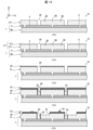
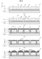
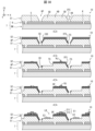
- FIG. 12 is a flowchart schematically showing a method for manufacturing a light emitting device in Example 1.
- FIG. 13 is a plan view schematically showing a method for manufacturing a light emitting body included in a light emitting element in Example 1.
- 14 and 15 are cross-sectional views schematically showing a method for manufacturing a light emitting element in Example 1.
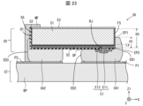
- FIG. 16 is a cross-sectional view showing an example of the structure of the template substrate.
- the bottom diagram among the plurality of diagrams shown along the flow of processing from top to bottom is a side view showing the end surface of the light emitting element 30 for convenience of explanation.
- a semiconductor substrate 10 is prepared.
- the semiconductor substrate 10 includes a template substrate 7 and a plurality of bar-shaped base semiconductor portions S11 arranged above the template substrate 7 in the X direction.
- the template substrate 7 includes, for example, a base substrate BK and a striped mask 6.
- the mask 6 is formed above the base substrate BK and has an opening K and a mask portion 5.
- the semiconductor substrate 10 having the first type semiconductor portion S1 may be prepared by forming the first type portion S12 above the base semiconductor portion S11.
- the base semiconductor portion S11 and the first type portion S12 may be successively formed above the template substrate 7 to prepare the semiconductor substrate 10 having the first type semiconductor portion S1.
- the semiconductor substrate 10 is prepared by forming the base semiconductor portion S11 on the template substrate 7 using the ELO method and further forming the first type portion S12, but the present invention is not limited thereto.
- the semiconductor substrate 10 can be prepared by performing various treatments on the base substrate BK.
- the specific method of preparing the semiconductor substrate 10 is not particularly limited, and the semiconductor substrate 10 of Example 1 may be prepared by processing a semi-finished product of the semiconductor substrate 10 in the middle of forming the semiconductor substrate 10. Also falls within the scope of this disclosure. This also applies to the following embodiments, although repeated explanation will be omitted.
- the template substrate 7 includes a base substrate BK and a mask 6 located above the base substrate BK. As shown in FIG. 16, the template substrate 7 may have a configuration in which a seed portion 3 and a mask 6 are formed in this order on the main substrate 1, or a multilayer base portion 4 (buffer portion) may be formed on the main substrate 1. 2 and the seed portion 3) and the mask 6 may be formed in this order.
- the seed portion 3 may be formed locally (for example, in a stripe shape) so as to overlap the opening K of the mask 6 in a plan view. Seed portion 3 may include a nitride semiconductor formed at a low temperature of 600° C. or lower.
- the template substrate 7 may have a configuration in which a mask 6 is formed on the main substrate 1 (for example, a SiC bulk crystal substrate or a GaN bulk crystal substrate).
- the base substrate BK may include at least the main substrate 1.
- the base substrate BK may include the main substrate 1 and the seed portion 3 located above the main substrate 1, and may include the main substrate 1 and the base portion 4 located above the main substrate 1.
- the main substrate 1 a different type of substrate having a lattice constant different from that of the GaN-based semiconductor can be used.
- the heterogeneous substrate include a single crystal silicon (Si) substrate, a sapphire (Al 2 O 3 ) substrate, a silicon carbide (SiC) substrate, and the like.
- the plane orientation of the main substrate 1 is, for example, the (111) plane of a silicon substrate, the (0001) plane of a sapphire substrate, or the 6H-SiC (0001) plane of a SiC substrate. These are just examples, and the main substrate 1 may be made of any material and have a surface orientation that allows the first type semiconductor portion S1 to be grown by the ELO method.
- a SiC (bulk crystal) substrate, a GaN (bulk crystal) substrate, or an AlN (bulk crystal) substrate can also be used.
- a buffer portion 2 and a seed portion 3 can be provided in this order from the main substrate 1 side.
- a silicon substrate is used as the main substrate 1 and a GaN-based semiconductor is used as the seed part 3 since both (the main substrate and the seed part) melt together, for example, at least one of the AlN layer and the SiC (silicon carbide) layer
- the buffer section 2 may have at least one of the effect of increasing the crystallinity of the seed section 3 and the effect of relaxing the internal stress of the first type semiconductor section S1. If the main substrate 1 that does not melt together with the seed part 3 is used, a configuration in which the buffer part 2 is not provided is also possible.
- the seed section 3 is not limited to the configuration in which the entire mask section 5 overlaps. Since the seed portion 3 only needs to be exposed through the opening K, the seed portion 3 may be formed locally so as not to overlap part or all of the mask portion 5.
- the opening K of the mask 6 has the function of a growth start hole that exposes the seed part 3 and starts the growth of the first type semiconductor part S1
- the mask part 5 of the mask 6 has the function of a growth start hole that exposes the seed part 3 and starts the growth of the first type semiconductor part S1. It functions as a selective growth mask for directional growth.
- the mask 6 may be a mask layer, and may be a mask pattern including the mask portion 5 and the opening K.
- a silicon oxide film (SiOx), a titanium nitride film (TiN, etc.), a silicon nitride film (SiNx), a silicon oxynitride film (SiON), or a metal film with a high melting point (for example, 1000 degrees or more) can be used.
- a single layer film containing any one of these or a laminated film containing at least two of these can be used.
- a silicon oxide film having a thickness of approximately 100 nm to 4 ⁇ m (preferably approximately 150 nm to 2 ⁇ m) is formed on the entire surface of the seed portion 3 using a sputtering method, and a resist is applied to the entire surface of the silicon oxide film. Thereafter, the resist is patterned using a photolithography method to form a resist having a plurality of striped openings. After that, a portion of the silicon oxide film is removed using a wet etchant such as hydrofluoric acid (HF) or buffered hydrofluoric acid (BHF) to form a plurality of openings K, and the resist is removed by organic cleaning to form a mask 6. be done.
- a wet etchant such as hydrofluoric acid (HF) or buffered hydrofluoric acid (BHF)
- silicon nitride film can be deposited using sputtering equipment or PECVD (Plasma).
- PECVD Enhanced Chemical Vapor Deposition
- the thickness of the silicon nitride film can be approximately 5 nm to 4 ⁇ m.
- the longitudinal-shaped (slit-shaped) openings K can be arranged periodically in the X direction.
- the width of the opening K may be approximately 0.1 ⁇ m to 20 ⁇ m. The smaller the width of the opening K, the larger the width (size in the X direction) of the low defect portion SD (corresponding to the second portion B2 or the third portion B3).
- Abnormal locations such as pinholes in the mask portion 5 can be eliminated by performing organic cleaning or the like after film formation, and reintroducing the film into the film forming apparatus to form the same type of film. It is also possible to form a high-quality mask 6 using a general silicon oxide film (single layer) and using such a re-forming method.
- a silicon substrate for example, a 2-inch Si substrate having a (111) plane is used as the main substrate 1, and an AlN layer (approximately 30 nm to 300 nm, for example, 150 nm) is used in the buffer section 2.
- a GaN-based graded layer can be used for the seed portion 3
- a laminated mask in which a silicon oxide film (SiO 2 ) and a silicon nitride film (SiN) are formed in this order can be used for the mask 6.
- the GaN-based graded layer may include a first layer of Al 0.6 Ga 0.4 N layer (for example, 300 nm) and a second layer of GaN layer (for example, 1 to 2 ⁇ m).
- a CVD method plasma chemical vapor deposition method
- the thickness of the silicon oxide film is, for example, 0.3 ⁇ m
- the thickness of the silicon nitride film is, for example, It can be set to 70 nm.
- the width of the mask portion 5 (size in the X direction) can be 50 ⁇ m
- the width of the opening K (size in the X direction) can be 5 ⁇ m.
- Example 1 the base semiconductor portion S11 is formed on the template substrate 7 using the ELO method.
- the base semiconductor portion S11 was made of a GaN layer, and an ELO film of gallium nitride (GaN) was formed on the template substrate 7 using an MOCVD apparatus.
- the base semiconductor portion S11 is selectively grown (vertically grown) on the seed portion 3 exposed in the opening K (see FIG. 16), and subsequently grown laterally on the mask portion 5. Then, the lateral growth was stopped before the GaN crystal films grown laterally from both sides of the mask portion 5 came together.
- a plurality of base semiconductor parts S11 are formed by stopping the growth of semiconductor crystals (for example, GaN-based crystals) that grow close to each other on the mask part 5 before they meet each other. Thereby, a gap GP is formed between the base semiconductor parts S11 adjacent to each other in the X direction.
- the X direction is the ⁇ 11-20> direction (a-axis direction) of the GaN-based crystal
- the Y direction is the ⁇ 1-100> direction (m-axis direction) of the GaN-based crystal
- the Z2 direction is the ⁇ 1-100> direction (m-axis direction) of the GaN-based crystal.
- a vertically grown layer growing in the Z direction (c-axis direction) is formed on the seed portion 3 exposed from the opening K, and then a vertical growth layer is grown in the X direction (a-axis direction). Forms a lateral growth layer that grows.
- the thickness of the vertically grown layer is set to 10 ⁇ m or less, 5 ⁇ m or less, or 3 ⁇ m or less, the thickness of the horizontally grown layer can be kept low and the lateral film formation rate can be increased.
- the threading dislocation density of the low defect area SD (corresponding to the second part B2 or the third part B3) in the base semiconductor part S11 is equal to the threading dislocation density of the dislocation inheritance part HD (corresponding to the first part B1) in the base semiconductor part S11. It may be 1/5 or less (for example, 5 ⁇ 10 6 /cm 2 or less).
- the threading dislocation density here can be determined, for example, by performing CL measurement on the surface of the base semiconductor portion S11 (for example, by counting the number of black spots).
- the dislocation density can be expressed in units of [pieces/cm 2 ], and in this specification, "pieces" may be omitted and expressed as [/cm 2 ].
- the density of basal plane dislocations in the low defect portion SD may be 5 ⁇ 10 8 /cm 2 or less.
- the basal plane dislocation may be a dislocation extending in the in-plane direction of the c-plane (XY plane) of the base semiconductor portion S11.
- the basal plane dislocation density here can be obtained, for example, by dividing the base semiconductor portion S11 to expose the side surface of the low defect portion SD and measuring the dislocation density of this side surface by CL.
- the width (size in the X direction) of the base semiconductor portion S11 was 53 ⁇ m
- the width (size in the X direction) of the low defect portion SD was 24 ⁇ m
- the layer thickness (size in the Z direction) of the base semiconductor portion S11 was 5 ⁇ m.
- the width of the mask portion 5 can be set according to the specifications of the second type semiconductor portion S2, etc. (for example, about 10 ⁇ m to 200 ⁇ m).
- Example 1 adjacent base semiconductor parts S11 do not meet each other, and a plurality of bar-shaped base semiconductor parts S11 are formed on the template substrate 7 in line in the X direction, and the width of the gap GP (in the X direction) is The size) was approximately 5 ⁇ m.
- a first mold part S12 is formed above the base semiconductor part S11.
- a first type semiconductor section S1 is formed.
- the first type portion S12 may include, for example, a buffer layer (regrowth portion) containing an n-type GaN-based semiconductor.
- the first mold part S12 can be formed, for example, by MOCVD.
- the first mold section S12 includes the first contact section S121, the first cladding section S122, and the first light guide section S123.
- an n-type GaN layer can be used for the first contact part S121
- an n-type AlGaN layer can be used for the first cladding part S122
- an n-type GaN layer can be used for the first optical guide part S123.
- an active part AP is formed above the first type semiconductor part S1.
- the active portion AP can be formed, for example, by MOCVD.
- MOCVD Metal Organic Chemical Vapor Deposition
- an MQW (Multi-Quantum Well) structure including an InGaN layer can be used.
- the active part AP may typically have an MQW structure with 5 to 6 periods.
- the second type semiconductor portion S2 is formed so as to extend from above the active region AP to the side of the first type semiconductor portion S1.
- the second type semiconductor portion S2 can be formed, for example, by MOCVD.
- the second type semiconductor section S2 includes the second optical guide section S21, the electron blocking section S22, the second optical cladding section S23, and the second contact section S24.
- the second optical guide section S21 has a p-type GaN layer
- the electron blocking section S22 has a p-type AlGaN layer
- the second optical cladding section S23 has a p-type AlGaN layer
- the second contact section S24 has a p-type AlGaN layer.
- a p-type GaN layer can be used.
- a ridge stripe structure that is, a ridge portion RJ is formed using a photolithography method.
- the second type semiconductor part S2, the active part AP, and a part of the first type semiconductor part S1 are dug by etching or the like to expose a part of the upper surface of the first type semiconductor part S1.
- the exposed surface portion of the first type semiconductor portion S1 may be, for example, the first contact portion S121.
- a side surface of the first type semiconductor portion S1 that is formed by digging the first type semiconductor portion S1 and is located on the opposite side in the X direction with respect to the first side surface FS of the first type semiconductor portion S1. It is called 3-sided TS.
- the second side surface SS of the first type semiconductor portion S1 may be covered by the second type semiconductor portion S2, and the third side surface TS may not be covered by the second type semiconductor portion S2.
- the first side surface FS and the second side surface SS may be crystal planes, whereas the third side surface TS is a processed surface.
- a first contact electrode is formed on the second contact portion S24 of the ridge portion RJ.
- a first auxiliary electrode E12 is formed to cover the first contact electrode E11 and the insulating film DF.
- a second electrode E2 is formed on the upper surface of the exposed surface of the first type semiconductor portion S1.
- the second electrode E2 may include a second contact electrode and a second auxiliary electrode (not shown).
- the first electrode E1 (anode) and the second electrode E2 (cathode) include, for example, (i) a metal film containing at least one of Ni, Rh, Pd, Cr, Au, W, Pt, Ti, and Al ( A single layer film or a multilayer film selected from (ii) a conductive oxide film containing at least one of Zn, In, and Sn can be used.
- a single layer film or a laminated film containing, for example, an oxide or nitride of Si, Al, Zr, Ti, Nb, or Ta can be used.
- the first contact electrode E11 (p contact electrode) may be a Pd film with a thickness of 50 nm, for example.
- the first auxiliary electrode E12 may be a multilayer film in which, for example, a 100 nm thick Ti film, a 200 nm thick Ni film, and a 100 nm thick Au film are formed in this order.
- the second auxiliary electrode of the second electrode E2 may also have the same configuration as the first auxiliary electrode E12, and for example, a 100 nm thick Ti film may also serve as an n-contact electrode.
- the insulating film DF, the first electrode E1, and the second electrode E2 may be formed avoiding the portion where the open groove portion GS is formed, that is, the position where scribing is performed.
- the length of one insulating film DF in the Y direction, the length of one first electrode E1 in the Y direction, and the length of one second electrode E2 in the Y direction may each be smaller than the resonator length L1.
- a stacked body LB having the first type semiconductor portion S1, the second type semiconductor portion S2 including the ridge portion RJ, the first electrode E1, the second electrode E2, etc. is formed.
- the semiconductor substrate 10 having a plurality of bar-shaped stacked bodies LB can be formed.
- the second type semiconductor part S2, the active part AP, and the first type semiconductor part S1 are dug until, for example, the base semiconductor part S11 in the first type semiconductor part S1 is exposed, and a second electrode is formed on the base semiconductor part S11. E2 may also be formed.
- the laminate LB is cleaved on the template substrate 7 (m-plane cleavage of the first and second type semiconductor parts S1 and S2, which are nitride semiconductor layers), and a pair of A light emitting body 20 having cavity end faces F1 and F2 is formed.
- the laminate LB is bar-shaped, for example, the laminate LB is cleaved in a direction (X direction) orthogonal to the longitudinal direction (Y direction) of the laminate LB.
- a plurality of pieces obtained by dividing the laminate LB can each be used as the light emitting body 20.
- a gap open groove portion GS
- the laminate LB may be scribed (for example, a scribe groove serving as a cleavage starting point is formed).
- the specific method of scribing is not particularly limited, for example, the stacked body LB may be scribed using a scriber by applying a force in a direction parallel to the m-plane of the nitride semiconductor crystal in the second type semiconductor portion S2. You can go.
- the scriber may be a diamond scriber or a laser scriber.
- the pair of resonator end faces F1 and F2 may be formed by scribing the laminate LB and causing cleavage to proceed naturally.
- the base semiconductor portion S11 includes a GaN-based semiconductor
- the base substrate BK includes the main substrate 1 made of a material having a smaller coefficient of thermal expansion than the GaN-based semiconductor.
- the base semiconductor portion S11 may include GaN
- the base substrate BK may include a Si substrate or a SiC substrate.
- the film formation temperature is high, for example, 1000°C or higher, and internal stress is created in the base semiconductor part S11 by lowering the temperature to room temperature after film formation. occurs.
- This internal stress is caused, for example, by a difference in thermal expansion coefficient between the main substrate 1 and the base semiconductor portion S11.
- the thermal expansion coefficient of the main substrate 1 is smaller than that of the base semiconductor portion S11, tensile stress is generated in the base semiconductor portion S11.
- the main substrate 1 is a Si substrate and the constituent material of the base semiconductor portion S11 is GaN, tensile stress is generated in the base semiconductor portion S11.
- internal stress may also be generated in the base semiconductor portion S11 due to strain generated in the base semiconductor portion S11 due to a difference in lattice constant between the main substrate 1 and the base semiconductor portion S11.
- a laminate LB is scribed, internal stress in the base semiconductor portion S11 is released and tensile strain is generated at the cleavage starting point, so that cleavage progresses spontaneously.
- the resonator length L1 of the light emitting body 20 can be set to 100 ⁇ m.
- the main substrate 1 is not divided.
- the mask portion 5 does not need to be divided, and may be divided by the influence of cleavage of the stacked body LB.
- the base semiconductor portion S11 of each stacked body LB and the base substrate BK are chemically bonded. Therefore, the light emitter 20 is held by the base substrate BK and its position is maintained on the base substrate BK.
- Example 1 by forming the light emitting body 20 by cleavage, the volume of the laminate LB that disappears can be made smaller than when the open groove portion GS is formed by, for example, dry etching. Therefore, the semiconductor substrate 10 can be used efficiently (as an element).
- the resonator end faces F1 and F2 are formed by m-plane cleavage, so they have excellent planarity and perpendicularity to the c-plane (parallelism of the resonator end faces F1 and F2), and are coated with a high reflection film.
- High light reflectance can be obtained by Therefore, mirror loss can be reduced even with short cavity lengths of 200 ⁇ m or less, where mirror loss increases, and stable laser oscillation is possible even with short cavity lengths of 200 ⁇ m or less, where optical gain is small.
- the resonator end faces F1 and F2 corresponding to the light emission area EA are formed on the second part B2, which is the low-defect part SD, so that the flatness of the cleavage plane is excellent and a high light reflectance is achieved. Ru.
- the method for manufacturing a light emitting element in Example 1 includes a step of preparing a support substrate SK.
- the supporting substrate SK to be prepared may be used as long as the light emitter 20 can be mounted in a junction-down manner, and its specific configuration is not particularly limited, but an example will be described below.
- FIG. 17 is a plan view showing an example of the configuration of the support substrate.
- the support substrate SK includes a first bonding material CA1 that functions as a bonding layer between the first pad portion P1 and the second pad portion P2 having a conductive T-shape and the first pad portion P1. and a second bonding material CA2 that functions as a bonding layer with the second pad portion P2.
- the material of the substrate body portion BS in the support substrate SK include Si, SiC, AlN, and the like.
- the first bonding material CA1 and the second bonding material CA2 correspond to the above-mentioned bonding material CA, and are made of conductive materials having at least one of heat fluidity, pressure curability, thermosetting property, and photocuring property. It's good that it has been done.
- the first bonding material CA1 and the second bonding material CA2 may be, for example, solder.
- the support substrate SK may be formed as follows, for example. That is, a 4-inch Si substrate is used as the substrate body part BS, and the first pad part P1 and the second pad part P2 are formed by a wafer process using photolithography technology.
- the plurality of recesses HL can be provided in a matrix shape with a depth of 100 ⁇ m by reactive ion etching (RIE) or the like. Then, the first bonding material CA1 and the second bonding material CA2 are formed.
- the first pad part P1 and the second pad part P2 are each a multilayer film in which a Cr film with a thickness of 10 nm, a Pt film with a thickness of 25 nm, and an Au film with a thickness of 100 nm are formed in this order from the substrate main body part BS side. It may be.
- the first bonding material CA1 may be, for example, an AuSn bonding layer in which a 3000 nm thick AuSn film and a 100 nm thick Au film are formed in this order from the substrate main body BS side.
- the second bonding material CA2 may be made of the same material as the first bonding material CA1, and may be thicker than the first bonding material CA1.
- the material of the substrate body portion BS in the support substrate SK and the material of the base substrate BK in the semiconductor substrate 10 may be the same, for example, Si.
- the coefficient of thermal expansion of the support substrate SK and the coefficient of thermal expansion of the semiconductor substrate 10 can be made equal. This improves the accuracy of alignment between the support substrate SK and the semiconductor substrate 10, and reduces the possibility that defects will occur in the transfer due to temperature changes caused by heating and cooling during selective transfer.
- the mask portion 5 may be removed by etching using hydrofluoric acid, buffered hydrofluoric acid (BHF), or the like. That is, the mask portion 5 of the semiconductor substrate 10 may be removed before junction-down mounting on the support substrate SK. Thereby, the light emitting body 20 can be easily separated from the template substrate 7.
- the semiconductor substrate 10 has the gap GP, so that the mask portion 5 is partially exposed. Therefore, the mask portion 5 can be easily removed by etching.
- the semiconductor substrate 10 may be divided into appropriate sizes by dicing or the like, for example, into pieces of 10 mm square size. Further, the support substrate SK may be divided into appropriate sizes by dicing or the like. For example, the support substrate SK may be divided into pieces of 10 mm square so that the size is the same as the semiconductor substrate 10 that has been cut into pieces.
- the light emitting body 20 is junction-down mounted on the support substrate SK.
- a portion selected from the plurality of light emitting bodies 20 may be selectively transferred from the semiconductor substrate 10 to the support substrate SK so as to straddle the plurality of light emitting bodies 20, such as every second or third light emitting body.
- the light emitters 20 are individually separated by having a gap GP between the light emitters 20 and an open groove portion GS on the template substrate 7. Therefore, selective transfer can be easily performed.
- FIG. 18 is a perspective view schematically showing a light emitting substrate (semiconductor laser array) in which a plurality of light emitting bodies are bonded to a support substrate.
- the light emitting substrate 31 includes a support substrate SK and a plurality of light emitters 20.
- a plurality of light-emitting bodies 20 are arranged on the support substrate SK in a direction defining the cavity length (Y direction) and a direction perpendicular thereto (X direction) so that the directions of the cavity lengths are aligned. They may be arranged in a matrix.
- a reflective mirror film UF is formed on the resonator end faces F1 and F2 of the light emitter 20.
- the reflective mirror film UF is formed for reflectance adjustment, passivation, and the like.
- the reflective mirror film UF may be formed using a two-dimensional arrangement type light emitting substrate 31, and after dividing the light emitting substrate 31 into bar shapes, the reflective mirror film UF is formed using the formed bar-shaped light emitting substrates 31. may be formed.
- FIG. 19 is a perspective view showing an example of a bar-shaped light emitting substrate after being divided.
- a two-dimensional arrangement type light emitting substrate 31 as shown in FIG. 18 is horizontally divided (divided into rows extending in the X direction) to form a one-dimensional arrangement type (bar-shaped) light emitting substrate 31 as shown in FIG. 19. I can do it.
- the one-dimensional arrangement facilitates the formation of the reflective film UF on the pair of resonator end faces F1 and F2.
- the support substrate SK has a wide portion SH and a mounting portion SB.
- the light emitter 20 is located above the receiver SB so that the width direction (Y direction) of the receiver SB matches the resonator length direction.
- the pair of resonator end faces F1 and F2 of the light-emitting body 20 may protrude from the mounting portion SB in plan view.
- the mounting part SB is formed between two cutout parts C1 and C2 facing each other in the direction (Y direction) that defines the resonator length, and the resonator end face F1 is located on the cutout part C1, and the resonator
- the vessel end surface F2 is located on the notch C2.
- the cutout portions C1 and C2 are portions corresponding to the recesses HL in the support substrate SK before being divided.
- the shape of the cutout portions C1 and C2 can be, for example, rectangular in a plan view viewed in the Z1 direction.
- the light emitting substrate 31 may be further divided. Thereby, it is possible to form a plurality of light emitting elements 30 in which one or more light emitting bodies 20 are junction-down mounted on the support ST.
- FIG. 20 is a perspective view showing the configuration of the light emitting element in Example 1.
- FIG. 21 is a cross-sectional view showing the configuration of a light emitting element in Example 1.
- the light emitting element 30 is configured such that the light emitting body 20, the first bonding material CA1, the second bonding material CA2, and the first type semiconductor portion S1 are located above the active portion AP. and a support ST that supports the light emitting body 20 via first and second bonding materials CA1 and CA2.
- the support body ST includes a conductive first pad part P1 and a second pad part P2, the first electrode E1 is connected to the first pad part P1 via the first bonding material CA1, and the second electrode E2 is connected to the first pad part P1 through the first bonding material CA1. It is connected to the second pad portion P2 via the second bonding material CA2.
- the base portion BP which is the main body portion of the support ST, corresponds to a portion of the support substrate SK, which is obtained by dividing the substrate main body portion BS.
- the second bonding material CA2 is thicker than the first bonding material CA1, and the difference in thickness between the first bonding material CA1 and the second bonding material CA2 may be greater than or equal to the thickness of the second type semiconductor portion S2. This makes it easier to bond the first and second electrodes E1 and E2 to the first and second pad portions P1 and P2 located on the same plane.
- the light emitting element 30 functions as a COS (Chip on Submount).
- the first pad part P1 is located on the wide part SH, and the mounting part J1 whose length in the Y direction is larger than the resonator length L1, and the mounting part SB, which is located on the mounting part SB and whose length in the Y direction is larger than the resonator length L1.
- the second pad part P2 includes a contact part Q1 which is smaller than the length L1, a mounting part J2 which is located on the wide part SH, and whose length in the Y direction is larger than the resonator length L1, and a mounting part J2 which is located on the mounting part SB. and a contact portion Q2 whose length in the Y direction is smaller than the resonator length L1.
- the contact portions Q1 and Q2 are arranged in the X direction on the upper surface of the mounting portion SB, a first bonding material CA1 is formed on the contact portion Q1, and a second bonding material CA2 is formed on the contact portion Q2.
- the first bonding material CA1 contacts the first electrode E1 of the light emitter 20, and the second bonding material CA2 contacts the second electrode E2 of the light emitter 20.
- solder such as AuSi or AuSn can be used as AuSi or AuSn.
- the resonator end faces F1 and F2 of the light emitter 20 are covered with a reflective membrane UF, but among the side faces of the support ST, the faces parallel to the resonator end faces F1 and F2 (for example, the side face of the mounting part SB) ) may be formed with a dielectric film SF made of the same material as the reflective mirror film UF.
- the semiconductor substrate 10 and the support substrate SK are brought into contact with each other and a load is applied. Then, the first bonding material CA1 and the second bonding material CA2 are melted and held for a certain period of time, and then cooled to room temperature. Thereby, the semiconductor substrate 10 and the support substrate SK are in a state where they are bonded to each other. Specifically, the first electrode E1 and the first pad portion P1 are bonded by the first bonding material CA1, and the second electrode E2 and the second pad portion P2 are bonded by the second bonding material CA2.
- the first bonding material CA1 and the second bonding material CA2 having fluidity can wet and spread over the first pad portion P1 and the second pad portion P2, and can run up the side surface 20T of the light emitter 20.
- a part of the edge ED1 of the first bonding material CA1 may protrude from the light emitting body 20 in a plan view of the light emitting element 30 in the stacking direction of the first type semiconductor part S1 and the active part AP.
- Example 1 since the light emitting body 20 has a single-sided two-electrode structure, the first bonding material CA1 tends to protrude outward in the X direction from the light emitting body 20 in plan view.
- the first bonding material CA1 runs up along the second type semiconductor portion S2 located on the side of the first side surface FS.
- the run-up height H1 of the first bonding material CA1 may exceed the lower surface level LV of the first type semiconductor portion S1.
- the second type semiconductor part S2 is arranged from below the active part AP to the side of the first type semiconductor part S1 on the first side surface FS.
- the formation height H3 of the second type semiconductor portion S2 is greater than the run-up height H1 of the bonding material CA.
- the width W10 of the light emitting element 30 in the X direction may be 50 ⁇ m or less, and may be 20 ⁇ m or less.
- the width W10 may be the distance in the X direction between the third side surface TS and the outer surface of the second type semiconductor portion S2 located on the side of the first side surface FS.
- the light emitting element 30 may have a distance L11 in the X direction between the third side surface TS and the end surface PE1 of the first pad portion P1, and in this case, the first bonding material CA1 runs up the third side surface TS. It can be difficult to do.
- At least a portion of the third side surface TS may be covered with the insulating film DF, and at least a portion of the third side surface TS may be in contact with the insulating film DF.
- the first type semiconductor part S1 is closer to the first side surface FS than the first part (center part) B1 in the X direction (a-axis direction of the nitride semiconductor crystal), and has a lower threading dislocation density than the first part B1. It has a second part (wing part) B2.
- the ridge portion RJ overlaps the second portion B2 in a plan view, and each of the pair of cavity end faces F1 and F2 is an m-plane of a nitride semiconductor.
- the active part AP includes a light emitting area (light emitting part) EA located below the second part B2.
- the first type semiconductor portion S1 has an exposed portion ES below which the second type semiconductor portion S2 is not located.
- the exposed portion ES may be a portion formed by digging a portion of the first type semiconductor portion S1.
- a first electrode (anode) E1 is provided below the second type semiconductor portion S2, and a second electrode (cathode) E2 is provided below the exposed portion ES.
- the second type semiconductor portion S2 extends from below the active portion AP to the side of the first side surface FS of the first type semiconductor portion S1 and to the side of the second side surface SS.
- the second bonding material CA2 may run up along the second type semiconductor portion S2 located on the side of the second side surface SS.
- the third side surface TS which is the side surface located on the exposed portion ES side, is a surface formed by etching or the like, and does not need to be covered by the second type semiconductor portion S2.
- Example 1 In Example 1, the open groove portions GS were formed by cleaving the laminate LB, and the laminate LB was divided into a plurality of light emitting bodies 20.
- the present invention is not limited to this, and the multilayer body LB may be divided into a plurality of light emitting bodies 20 by forming the open groove portions GS by forming a plurality of trenches in the multilayer body LB.
- a plurality of trenches as the open groove portions GS can be formed by dry etching the stacked body LB. Thereby, a pair of resonator end faces F1 and F2 (etched mirrors) can be formed.
- the trench may be formed after the first electrode E1 and the second electrode E2 are formed, or the first electrode E1 and the second electrode E2 may be formed after the trench is formed.
- the active part AP may be arranged from below the first type semiconductor part S1 to the side of the first type semiconductor part S1, and activates at least a part of the first side surface FS.
- the part AP may be covered.
- the active portion AP may cover at least a portion of the second side surface SS of the first type semiconductor portion S1.
- the raw material for the active part AP can be supplied to the first side surface FS and the second side surface SS. Since the active part AP has a thin film thickness, it is difficult to form the active part AP on the surfaces of the first side surface FS and the second side surface SS in the first type semiconductor part S1.
- An active portion AP may exist between the second side surface SS and the second type semiconductor portion S2.
- the light emitter 20 may be a laser body (semiconductor laser chip) having a double-sided electrode structure.
- FIG. 22 is a perspective view showing the configuration of a light emitting element in another example of Example 1.
- FIG. 23 is a cross-sectional view showing the configuration of a light emitting element in another example of Example 1.
- a first electrode (anode) E1 is provided below the second type semiconductor portion S2, and a first electrode (anode) E1 is provided above the first type semiconductor portion S1.
- a second electrode (cathode) E2 may be provided.
- the light emitting body 20 does not need to have the exposed portion ES.
- the insulating film DF may cover the lower surface of the second type semiconductor portion S2.
- the second bonding material CA2 may be solder or may be a non-conductive material.
- the edge ED3 of the second bonding material CA2 may protrude from the light emitting body 20 in plan view.
- an insulating film D1 may be formed to cover the second side surface SS of the first type semiconductor portion S1 and the side surfaces of the active portion AP and the second type semiconductor portion S2. .
- the insulating film D1 may not be formed.
- the second electrode E2 formed on the back surface (the surface far from the support body ST) of the first type semiconductor portion S1 may be connected to the second pad portion P2 via the conductive film MF, for example.
- the second electrode E2 may be wire-bonded to the second pad portion P2.
- FIG. 24 is a cross-sectional view schematically showing a method for manufacturing a light emitting element in another example of Example 1.
- the insulating film DF is transferred from above the second type semiconductor portion S2 to the first type semiconductor portion S2. It may be formed so as to extend to the side of the semiconductor portion S1.
- the light emitting element 30 in another example of the first embodiment may include a first insulating film DF1 that covers a portion of the second type semiconductor portion S2 extending onto the first side surface FS.
- the first insulating film DF1 may be in contact with the second type semiconductor portion S2.
- first side surface FS there may be a portion on the first side surface FS where the second type semiconductor portion S2 is not located, and in this case, there may be a portion on the first side surface FS where the second type semiconductor portion S2 is not located. There may be a portion where the second type semiconductor portion S2 does not exist, and the first insulating film DF1 may be in contact with the first side surface FS in this portion.
- the second insulating film DF2 may be formed to cover the portion of the second type semiconductor portion S2 that extends over the second side surface SS.
- the second type semiconductor portion S2 may not exist between the second insulating film DF2 and the second side surface SS, and the second insulating film DF2 may be in contact with the second side surface SS in this portion.
- the first insulating film DF1 may be formed separately from the insulating film DF after the insulating film DF is formed above the second type semiconductor portion S2.
- the first insulating film DF1 can be formed before the light emitter 20 is transferred to the support substrate SK.
- the second insulating film DF2 may be formed at the same timing as the first insulating film DF1, or the second insulating film DF2 may not be formed.
- the insulating film DF may be formed from above the second type semiconductor portion S2 to the third side surface TS. Even if the first bonding material CA1 runs up the third side surface TS, the possibility that the first bonding material CA1 comes into contact with the first type semiconductor portion S1 can be effectively reduced.
- the first insulating film DF1 and the second insulating film DF2 can be formed in the same manner as described above.
- the adjacent laminate LB may be affected by the dry etching due to factors such as insufficient protection by resist. If the first side surface FS is covered only with the second type semiconductor portion S2, the first type semiconductor portion S1 may be exposed due to the influence of dry etching. On the other hand, by forming the insulating film DF or the first insulating film DF1 on the first side surface FS, it is possible to effectively reduce the possibility of unintended effects caused by dry etching.
- a template substrate 7 including the main substrate 1 and a mask 6 on the main substrate 1 may be used, and the template substrate 7 has a growth suppressing region (for example, it may include a region for suppressing crystal growth in the Z direction) and a seed region corresponding to the opening K.
- the base semiconductor portion S11 can also be formed using the ELO method on a template substrate having a growth suppression region and a seed region.
- FIG. 25 is a flowchart schematically showing a method for manufacturing a light emitting element in Example 2.
- FIG. 26 is a cross-sectional view schematically showing a method for manufacturing a light emitting element in Example 2.
- FIG. 27 is a plan view schematically showing a method for manufacturing a light emitting element in Example 2.
- Example 1 the stacked body LB was formed by forming the second type semiconductor portion S2 on the first type semiconductor portion S1 having the low defect portion SD and the dislocation inheritance portion HD.
- Example 2 the portion above the opening K (dislocation inheritance portion HD) in the first type semiconductor portion S1 formed on the template substrate 7 is removed, and a first type semiconductor portion S1 having the low defect portion SD is removed.
- a type 2 semiconductor section S2 is formed.
- Example 2 an example will be described in which a light emitting body 20 having a double-sided electrode structure is formed, but it is also possible to form a light emitting body 20 having a single-sided two-electrode structure as described above. For example, it is also possible to form the light emitting body 20 having a single-sided two-electrode structure using the low defect portion SD by forming the first type semiconductor portion S1 to have a wide width.
- the semiconductor substrate 10 is prepared.
- the semiconductor substrate 10 includes a plurality of bar-shaped first-type semiconductors formed by stopping the growth of a plurality of semiconductor crystals (for example, GaN-based crystals) that grow close to each other on the mask portion 5 before meeting each other. It may have a section S1.
- a plurality of trenches are formed in the first type semiconductor part S1 by etching so as to remove the joint part between the first type semiconductor part S1 and the base substrate BK of the template substrate 7 (for example, the joint part with the seed part 3: see FIG. 16).
- Form TR This divides the first type semiconductor section S1.
- Trench TR may extend in the longitudinal direction of opening K (Y direction).
- the trench TR may form the fourth side surface FTS, which is one of the two side surfaces of the first type semiconductor portion S1 that face each other in the a-axis direction.
- Example 2 the first type semiconductor part S1 is loosely coupled to the mask part 5, so after forming the active part AP and the second type semiconductor part S2, the stacked structure is formed on the template substrate 7.
- An anchor film AF may be formed so that the position of LB does not change.
- the anchor film AF is in contact with the side surface of the second type semiconductor section S2 or the side surface of the first type semiconductor section S1, as well as the mask section 5, and anchors the stacked body LB to the template substrate 7.
- dielectric films such as silicon oxide film, silicon nitride film, aluminum oxide film, silicon oxynitride film, aluminum oxide-silicon film, aluminum oxynitride film, zirconium oxide film, titanium oxide film, tantalum oxide film, etc. etc. can be used.
- the anchor film AF may remain on the template substrate 7 or may accompany the light emitters 20. Since the anchor film AF has no conductivity, even if it ultimately remains on the chip, there is no risk of causing electrical leakage or the like.
- a second type semiconductor part S2 having an active part AP and a ridge part RJ is formed above the first type semiconductor part S1.
- the second type semiconductor portion S2 may be in contact with at least a portion of the fourth side surface FTS.
- the first electrode E1 is formed.
- an open groove portion GS is formed in the stacked body LB.
- the open groove portion GS may be a gap created by cleavage, or may be a trench TR.
- the subsequent steps may be the same as those in Example 1 and Alternative Configuration Example 1C described above.
- the anchor film AF and the mask portion 5 may be removed before the light emitter 20 is junction-down mounted on the support substrate SK.
- the anchor film AF is positioned so as to cover the first side surface FS, it is possible to effectively reduce the possibility that the first bonding material CA1 and the first side surface FS will come into contact with each other.
- FIG. 28 is a plan view schematically showing a method for manufacturing a light emitting element in another example of Example 2.
- the first type semiconductor portion S1 may be formed into a planar shape using the ELO method, and then a plurality of bar-shaped first type semiconductor portions S1 may be formed by etching or the like.
- a first type semiconductor portion S1 is formed above the prepared template substrate 7 by the ELO method.
- semiconductor crystals for example, GaN-based crystals
- semiconductor crystals for example, GaN-based crystals
- a plurality of first type semiconductor parts S1 are formed by removing the semiconductor crystals at the meeting parts.
- the meeting occurs approximately at the center of the adjacent openings K (the center of the mask portion 5).
- a plurality of trenches TR extending in the Y direction in the first type semiconductor portion S1 which is planar in plan view, a plurality of bar-shaped first type semiconductor portions S1 are formed.
- the dislocation inheritance portion HD may or may not be removed by the trench TR.
- Trench TR may be formed such that mask portion 5 is removed to expose base substrate BK in plan view, or may be formed such that mask portion 5 is left.
- the subsequent steps may be the same as in Example 2 above.
- FIG. 29 is a cross-sectional view showing an example of lateral growth of a base semiconductor portion.
- FIG. 30 is a cross-sectional view schematically showing a method for manufacturing a light emitting element in Example 3.
- the base semiconductor portion S11 formed by the ELO method can be grown laterally as follows. As shown in FIG. 29, an initial growth part SL is formed on the seed part 3 (upper GaN layer) exposed from the opening K, and then a base semiconductor part S11 is laterally grown from the initial growth part SL. It's fine.
- the initial growth portion SL serves as a starting point for lateral growth of the base semiconductor portion S11.
- the initial growth is started immediately before the edge of the initial growth portion SL rides on the top surface of the mask portion 5 (at the stage where it is in contact with the upper end of the side surface of the mask portion 5), or immediately after the edge rides on the top surface of the mask portion 5.
- the film formation of the portion SL may be stopped (that is, at this timing, the ELO film formation conditions may be switched from the c-axis direction film formation conditions to the a-axis direction film formation conditions).
- the lateral film formation is performed from the state where the initial growth part SL slightly protrudes from the mask part 5, it is possible to reduce the amount of material consumed in growing the base semiconductor part S11 in the thickness direction.
- the base semiconductor portion S11 can be laterally grown at high speed.
- the initial growth portion SL can have a thickness of, for example, 0.5 ⁇ m or more and 4.0 ⁇ m or less.
- the first side surface FS which is the side surface closer to the ridge portion RJ in the first type semiconductor portion S1, includes a first inclined surface IFS that is inclined toward the ridge portion RJ. It's okay to stay.
- the second type semiconductor portion S2 may cover the first inclined surface IFS.
- the first type semiconductor portion S1 may include, on the second side surface SS, a second inclined surface ISS that is inclined toward the ridge portion RJ.
- the second type semiconductor portion S2 may cover the second inclined surface ISS.
- Example 3 by having the first inclined surface IFS, the second type semiconductor part S2 can be easily formed from above the active part AP to the side of the first type semiconductor part S1. Furthermore, it is easy to form the insulating film DF from above the second type semiconductor portion S2 to the sides of the first type semiconductor portion S1.
- the insulating film DF may be formed from above the second type semiconductor part S2 to the side of the first type semiconductor part S1, and in this case, at least a part of the first inclined surface IFS.
- the insulating film DF may be located above in the normal direction.
- the insulating film DF may cover at least a portion of the second type semiconductor portion S2 formed on the first inclined surface IFS.
- the first insulating film DF1 formed separately from the insulating film DF may cover at least a portion of the first inclined surface IFS.
- the first inclined surface IFS may be a crystal plane, for example, the (11-22) plane of a nitride semiconductor crystal, or the (11-2 ⁇ ) plane ( ⁇ is an integer).
- the height H4 of the first inclined surface IFS in the Z2-axis direction may be greater than or equal to 0.1 times and less than or equal to 0.9 times the height H11 of the first type semiconductor portion S1 (see FIG. 11).
- the first inclined surface IFS is not limited to a crystal surface, but may be a processed surface.
- Example 3 since the first type semiconductor portion S1 has the first inclined surface IFS, it is possible to easily form the insulating film DF so as to reach the first inclined surface IFS. By forming the insulating film DF so as to reach the first inclined surface IFS, it is possible to effectively reduce the possibility of unintended effects caused by dry etching on the stacked body LB. As a result, when the light emitter 20 is junction-down mounted on the support substrate SK, the possibility of short-circuiting between the first electrode E1 and the first type semiconductor portion S1 via the first bonding material CA1 can be effectively reduced. I can do it.
- FIG. 31 is a flowchart schematically showing a method for manufacturing a light emitting element in Example 4.
- FIG. 32 is a cross-sectional view schematically showing a method for manufacturing a light emitting element in Example 4.
- FIG. 33 is a cross-sectional view schematically showing a method for manufacturing a light emitting element in Example 4.
- a first type semiconductor portion S1, an active portion AP, and a second type semiconductor portion S2 are formed in this order on a base substrate BK.
- the method includes a step of preparing a substrate, and a step of forming an insulating film (first insulating film DF1) on at least one side surface of the first type semiconductor part S1, the active part AP, and the second type semiconductor part S2.
- the active part AP and the second type semiconductor part S2 may not be formed so as to wrap around the first side surface FS.
- a first insulating film DF1 is formed to cover at least one side surface of the first type semiconductor portion S1, the active portion AP, and the second type semiconductor portion S2.
- a second insulating film DF2 may be formed to cover the second side surface SS.
- the method for manufacturing a light emitting device in Example 4 further includes the step of preparing a support substrate SK, and the step of preparing a light emitting body 20 including at least a portion of each of the first type semiconductor portion S1, the active portion AP, and the second type semiconductor portion S2. , a step of bonding the first type semiconductor portion S1 to the support substrate SK via the first bonding material CA1 and the second bonding material CA2 so that the first type semiconductor portion S1 is located above the active portion AP.
- a part of the second type semiconductor part S2, the active part AP, and the first type semiconductor part S1 is dug by etching or the like to expose a part of the upper surface of the first type semiconductor part S1. This forms the exposed portion ES.
- An insulating film may not be formed on the third side surface TS.
- a ridge portion RJ is formed in the second type semiconductor portion S2. After that, a first electrode E1 and a second electrode E2 are formed.
- the laminate LB is divided to form a light emitting body 20 having a two-electrode structure on one side.
- a cross section of the active part AP that is parallel to the thickness direction of the active part AP and intersects with the first side surface FS appears. This includes the step of dividing into multiple parts.
- a step of separating the light emitter 20 from the base substrate BK is performed.
- the light emitting element 30 is formed by junction-down mounting the light emitting body 20 on the support substrate SK. Other details of each step can be understood with reference to Examples 1 to 3 above.
- Example 4 it is possible to collectively form the insulating film on the side surfaces of the plurality of light emitters 20 on the base substrate BK (in other words, to collectively form the insulating film at the wafer level).
- FIG. 34 is a perspective view showing the configuration of a light emitting body in Example 5.
- FIG. 35A is a partial cross-sectional view of a light emitter in Example 5.
- FIG. 35B is a partial plan view of the light emitter in Example 5.
- FIG. 36 is a plan view schematically showing a method for manufacturing a light emitting element in Example 5.
- the light emitter 20 may be, for example, a light emitting diode. As shown in FIGS. 34 to 36, the light emitter 20 includes at least a portion of each of a first type semiconductor portion S1, an active portion AP, and a second type semiconductor portion S2.
- the second type semiconductor portion S2 is arranged from above the active portion AP to the side of the first type semiconductor portion S1.
- the second type semiconductor portion S2 may cover at least a portion of the first side surface FS of the first type semiconductor portion S1.
- the active part AP includes a nitride semiconductor and emits light in the c-axis direction of the active part AP.
- the first type semiconductor portion S1 includes a base semiconductor portion S11 and a first type portion S12 including a regrowth layer (for example, a buffer layer containing an n-type GaN-based semiconductor) formed on the base semiconductor portion S11. good.
- a regrowth layer for example, a buffer layer containing an n-type GaN-based semiconductor
- the side surfaces of the chip may be physically and chemically damaged by the ion atoms of the etchant.
- the chip size becomes about 20 ⁇ m or less, the ratio of side damage to the light emitting area of the chip increases. Therefore, damage to the side surface of the active part AP may become serious.
- Example 5 trenches TR for dividing the first type semiconductor part S1 are formed before forming the active part AP, and etching for dividing the element does not have to be performed after forming the active part AP. . Thereby, the condition of the side surfaces of the active part AP and the second type semiconductor part S2 can be improved.
- the active part AP may include the light emitting part LS, and the entire light emitting part LS may overlap with the second part B2 (low defect part SD) in plan view. Since etching damage to the active part AP can be avoided, the size Ly of one side of the light emitting part LS may be small.
- the size Ly of one side of the light emitting part LS (for example, the side perpendicular to the adjacent trench TR) may be 80 ⁇ m or less, 40 ⁇ m or less, 20 ⁇ m or less, or 10 ⁇ m or less. It may be 5 ⁇ m or less.
- the etching for the first type semiconductor portion S1 is dry etching, and this dry etching may be stopped at the mask portion 5.
- mask portion 5 functions as an etching stopper and is exposed at the bottom of trench TR.
- the etching does not necessarily have to stop at the surface of the mask portion 5, but it is sufficient that the etching stops within the mask portion 5.
- the mask portion 5 is formed of a material that is less likely to be etched than the first type semiconductor portion S1, and a portion of the mask portion 5 may be etched as long as it can serve to stop etching.
- the raw material flows from above the active region AP to the side of the first side surface FS in the first type semiconductor portion S1 and to the side of the second side surface SS.
- the second type semiconductor portion S2 can be formed so as to reach the second type semiconductor portion S2.
- the second type semiconductor portion S2 may be formed to extend to the side of the end face 20F (see FIG. 2) of the light emitting body 20 in the first type semiconductor portion S1.
- the second type semiconductor part S2, the active part AP, and a part of the first type semiconductor part S1 are dug by etching or the like to expose a part of the upper surface of the first type semiconductor part S1.
- the third side surface TS does not need to be covered by the second type semiconductor section S2.
- a first electrode E1 and a second electrode E2 are formed. This forms the light emitter 20.
- the subsequent steps may be the same as those in Example 1 and the like described above.
- the stacked body LB is formed into a plurality of light emitting bodies 20 by forming the open groove part GS. May be divided.
- the open groove portion GS may be formed by cleaving.
- the open trench portion GS may be a trench TR formed by etching.
- FIG. 37 is a plan view schematically showing a method for manufacturing a light emitting element in another example of Example 5. As shown in FIG. 37, the portion above the opening K in the first type semiconductor portion S1 (dislocation inheritance portion HD) is removed by at least one of the plurality of trenches TR formed in the first type semiconductor portion S1, An active portion AP and a second type semiconductor portion S2 are formed on the first type semiconductor portion S1 having the low defect portion SD.
- an anchor film AF may be formed on the template substrate 7 so that the position of the stacked body LB does not change. For example, by forming the anchor film AF on the entire surface by sputtering or electron beam deposition (EB) using a resist mask, and then removing the resist mask, unnecessary portions of the anchor film AF can be lifted off.
- EB electron beam deposition
- Example 5 the light emitting element 30 is explained by exemplifying an LED element that emits light in the c-axis direction of the active part AP, but the invention is not limited to this, and in another example of Example 5, the light emitting element 30 is It may be a vertical cavity surface emitting laser element (VCSEL) that emits light in the c-axis direction of the active region AP.
- VCSEL vertical cavity surface emitting laser element
- FIG. 38 is a plan view schematically showing a method for manufacturing a light emitting element in Example 6.
- the base semiconductor portion S11 was formed by the ELO method.
- a sapphire substrate may be used as the base substrate BK, and a semiconductor layer containing a nitride semiconductor is formed in a planar manner above the sapphire substrate. It may be formed.
- the semiconductor substrate 10 does not need to have the mask 6 on the GaN substrate.
- a semiconductor part formed by a general method is referred to as a semiconductor part SG.
- the semiconductor portion SG is, for example, a semiconductor layer containing a general nitride semiconductor epitaxially grown in the vertical direction on a growth substrate.
- the semiconductor part SG may be used as the first type semiconductor part S1, or the first type semiconductor part including the semiconductor part SG and the first type part S12 can be formed by appropriately forming the first type part S12 on the semiconductor part SG. S1 may also be formed. As a result, the first type semiconductor portion S1 has a first side surface FS.
- an active part AP is formed above the first type semiconductor part S1.
- a second type semiconductor part S2 is formed extending from above the active part AP to the sides of the first type semiconductor part S1.
- the light emitting body 20 is, for example, a laser body, a ridge portion RJ is formed, and a part of the second type semiconductor portion S2, active portion AP, and first type semiconductor portion S1 is etched or the like to form a first type semiconductor portion S1. A part of the upper surface of the semiconductor portion S1 is exposed. Then, a first electrode E1 and a second electrode E2 are formed.
- the subsequent steps can be performed in the same manner as in Example 1 described above. Therefore, illustrations and detailed explanations will be omitted.
- the light emitting body 20 may be peeled off from the base substrate BK by various methods, for example, by a laser lift-off method. Furthermore, a fragile layer (boron nitride) may be formed between the base substrate BK and the semiconductor portion SG to facilitate mechanical separation. A sacrificial layer (InGaN) may be formed to enable lift-off by photoelectrochemical etching.
Abstract
In the present invention, a light-emitting element comprises: a light-emitting body that includes a first-type semiconductor unit that has a first side surface and a first-type electrical conductivity, an active part positioned below the first-type semiconductor unit, and a second-type semiconductor unit that has a second-type electrical conductivity and is disposed to reach the side of the first type semiconductor unit from below the active part; (ii) an electrically conductive bonding member; and (iii) a support that is positioned below the light-emitting body, and that supports the light-emitting body with the electrically conductive bonding material interposed therebetween so that the first-type semiconductor unit is positioned above the active part.
Description
本開示は発光素子等に関する。
The present disclosure relates to light emitting devices and the like.
一般に、発光ダイオード等の発光素子は、個片化された発光体(ダイと称されることがある)を基板等の支持体に実装して製造されることがある。例えば、成長用基板上で半導体層を積層して形成された発光体の表面側の電極と支持体の電極とを、はんだ等の導電性接合材を介して接合する(いわゆるフリップチップボンディングする)実装方式が知られている(特許文献1を参照)。このような実装方式は「ジャンクションダウン実装」とも称される。
In general, light emitting elements such as light emitting diodes are sometimes manufactured by mounting individualized light emitting bodies (sometimes referred to as dies) on a support such as a substrate. For example, an electrode on the surface side of a light emitting body formed by laminating semiconductor layers on a growth substrate and an electrode on a support are bonded via a conductive bonding material such as solder (so-called flip-chip bonding). A mounting method is known (see Patent Document 1). Such a mounting method is also called "junction down mounting."
本開示の一態様における発光素子は、第1側面を有し、第1型導電性を有する第1型半導体部と、前記第1型半導体部の下方に位置する活性部と、第2型導電性を有し、前記活性部の下方から前記第1型半導体部の側方に至るように配された第2型半導体部と、を含む発光体と、導電性接合材と、前記発光体の下方に位置し、前記第1型半導体部が前記活性部よりも上側に位置するように、前記導電性接合材を介して前記発光体を支持する支持体と、を備えている。
A light emitting element according to an aspect of the present disclosure includes a first type semiconductor portion having a first type conductivity and a first side surface, an active portion located below the first type semiconductor portion, and a second type conductivity. a second type semiconductor part having a conductive bonding material and a second type semiconductor part disposed from below the active part to a side of the first type semiconductor part; a support body located below and supporting the light emitting body via the conductive bonding material so that the first type semiconductor part is located above the active part.
また、本開示の一態様における発光素子の製造方法は、ベース基板上に第1側面を有する第1型半導体部が形成された半導体基板を準備する工程と、前記第1型半導体部の上方に活性部を形成する工程と、前記活性部の上方から前記第1型半導体部の側方に至るように配された第2型半導体部を形成する工程と、支持基板を準備する工程と、前記第1型半導体部、前記活性部、および前記第2型半導体部それぞれの少なくとも一部を含む発光体を、前記第1型半導体部が前記活性部よりも上側に位置するように、導電性接合材を介して前記支持基板に接合する工程とを含む。
Further, a method for manufacturing a light emitting element according to an aspect of the present disclosure includes the steps of: preparing a semiconductor substrate in which a first type semiconductor portion having a first side surface is formed on a base substrate; a step of forming an active part; a step of forming a second type semiconductor part disposed from above the active part to a side of the first type semiconductor part; a step of preparing a support substrate; A light emitting body including at least a portion of each of the first type semiconductor part, the active part, and the second type semiconductor part is connected to a conductive junction such that the first type semiconductor part is located above the active part. and a step of bonding to the support substrate via a material.
また、本開示の一態様における発光素子の製造方法は、ベース基板上に第1型半導体部、活性部および第2型半導体部がこの順に形成された半導体基板を準備する工程と、前記第1型半導体部、前記活性部および前記第2型半導体部の少なくとも1つの側面に絶縁膜を形成する工程と、支持基板を準備する工程と、前記第1型半導体部、前記活性部、および前記第2型半導体部それぞれの少なくとも一部を含む発光体を、前記第1型半導体部が前記活性部よりも上側に位置するように、導電性接合材を介して前記支持基板に接合する工程とを含む。
Further, a method for manufacturing a light emitting device according to an aspect of the present disclosure includes the steps of: preparing a semiconductor substrate in which a first type semiconductor portion, an active portion, and a second type semiconductor portion are formed in this order on a base substrate; a step of forming an insulating film on at least one side surface of the type semiconductor section, the active section, and the second type semiconductor section; a step of preparing a supporting substrate; bonding a light emitting body including at least a portion of each type 2 semiconductor part to the supporting substrate via a conductive bonding material such that the first type semiconductor part is located above the active part; include.
以下、本開示の実施の形態について図面を参照して説明する。なお、以下の記載は本開示の趣旨をよりよく理解させるためのものであり、特に指定のない限り、本開示を限定するものではない。本明細書において特記しない限り、数値範囲を表す「A~B」は、「A以上B以下」を意味する。また、本出願における各図面に記載した構成の形状および寸法(長さ、幅等)は、実際の形状および寸法を必ずしも反映させたものではなく、図面の明瞭化および簡略化のために適宜変更している。換言すれば、図面において、各部材のサイズ等を適宜誇張して示している場合がある。
Hereinafter, embodiments of the present disclosure will be described with reference to the drawings. It should be noted that the following description is provided for better understanding of the gist of the present disclosure, and does not limit the present disclosure unless otherwise specified. Unless otherwise specified herein, the numerical range "A to B" means "A to B". In addition, the shapes and dimensions (length, width, etc.) of the structures described in each drawing in this application do not necessarily reflect the actual shapes and dimensions, and may be changed as appropriate for clarity and simplification of the drawings. are doing. In other words, in the drawings, the size of each member may be appropriately exaggerated.
〔発光素子〕
図1は、本開示の一実施形態における発光素子の構成を概略的に示す断面図である。図1に示すように、本実施形態における発光素子30は、発光体20と、導電性を有する接合材(導電性接合材)CAと、接合材CAを介して発光体20を支持する支持体ST(例えばサブマウント)とを備えている。 [Light emitting element]
FIG. 1 is a cross-sectional view schematically showing the configuration of a light emitting element in an embodiment of the present disclosure. As shown in FIG. 1, the light-emittingelement 30 in this embodiment includes a light-emitting body 20, a bonding material having conductivity (conductive bonding material) CA, and a support that supports the light-emitting body 20 via the bonding material CA. ST (for example, submount).
図1は、本開示の一実施形態における発光素子の構成を概略的に示す断面図である。図1に示すように、本実施形態における発光素子30は、発光体20と、導電性を有する接合材(導電性接合材)CAと、接合材CAを介して発光体20を支持する支持体ST(例えばサブマウント)とを備えている。 [Light emitting element]
FIG. 1 is a cross-sectional view schematically showing the configuration of a light emitting element in an embodiment of the present disclosure. As shown in FIG. 1, the light-emitting
発光体20は、(i)第1側面FSを有し、第1型導電性を有する第1型半導体部S1と、(ii)第1型半導体部S1の下方に位置する活性部APと、(iii)第2型導電性を有し、活性部APの下方から第1型半導体部S1の側方に至るように配された第2型半導体部S2と、を含む。ここでは、発光体20から支持体STへの方向を下方向(Z1軸方向負側)とする。支持体STは、発光体20の下方に位置し、第1型半導体部S1が活性部APよりも上側に位置するように、接合材CAを介して発光体20を支持する。
The light emitting body 20 includes (i) a first type semiconductor portion S1 having a first side surface FS and having first type conductivity; (ii) an active portion AP located below the first type semiconductor portion S1; (iii) a second type semiconductor part S2 having second type conductivity and arranged from below the active part AP to the side of the first type semiconductor part S1; Here, the direction from the light emitter 20 to the support ST is defined as the downward direction (negative side in the Z1 axis direction). The support body ST is located below the light emitter 20 and supports the light emitter 20 via the bonding material CA so that the first type semiconductor portion S1 is located above the active portion AP.
第1型半導体部S1が第1型半導体層であってよく、第2型半導体部S2が第2型半導体層であってよく、活性部APが活性層であってもよい。発光体20は例えば半導体レーザダイオード(端面発光型または面発光型のレーザダイオード)であってよく、発光ダイオードであってもよい。第1型半導体部S1はn型導電性を有していてよく、第2型半導体部S2はp型導電性を有していてよい。これに限定されず、第1型半導体部S1がp型導電性を有し、第2型半導体部S2がn型導電性を有していてもよい。
The first type semiconductor portion S1 may be a first type semiconductor layer, the second type semiconductor portion S2 may be a second type semiconductor layer, and the active portion AP may be an active layer. The light emitter 20 may be, for example, a semiconductor laser diode (an edge-emitting type or a surface-emitting type laser diode), or a light emitting diode. The first type semiconductor portion S1 may have n-type conductivity, and the second type semiconductor portion S2 may have p-type conductivity. The present invention is not limited to this, and the first type semiconductor portion S1 may have p-type conductivity, and the second type semiconductor portion S2 may have n-type conductivity.
第1型半導体部S1および第2型半導体部S2は、窒化物半導体(例えば、GaN系半導体)を含んでいてよい。窒化物半導体は、例えば、AlxGayInzN(0≦x≦1;0≦y≦1;0≦z≦1;x+y+z=1)と表すことができ、具体例として、GaN系半導体、AlN(窒化アルミニウム)、InAlN(窒化インジウムアルミニウム)、InN(窒化インジウム)を挙げることができる。GaN系半導体とは、ガリウム原子(Ga)および窒素原子(N)を含む半導体であり、典型的な例として、GaN、AlGaN、AlGaInN、InGaNを挙げることができる。
The first type semiconductor portion S1 and the second type semiconductor portion S2 may include a nitride semiconductor (for example, a GaN-based semiconductor). A nitride semiconductor can be expressed as, for example, AlxGayInzN (0≦x≦1; 0≦y≦1; 0≦z≦1; x+y+z=1), and specific examples include GaN-based semiconductors and AlN (aluminum nitride). , InAlN (indium aluminum nitride), and InN (indium nitride). A GaN-based semiconductor is a semiconductor containing gallium atoms (Ga) and nitrogen atoms (N), and typical examples include GaN, AlGaN, AlGaInN, and InGaN.
第1型半導体部S1は、ノンドープ型(i型)の半導体部を含んでいてもよい。第1型半導体部S1は、ドープ型の半導体部を含んでいてよい。第1型半導体部S1における活性部APと接する部分はドナーを含むn型の半導体部であってよい。第2型半導体部S2は、ノンドープ型(i型)の半導体部を含んでいてもよい。例えば、第2型半導体部S2における活性部APと接する部分が、ノンドープ型(i型)の半導体部となっていてもよい。
The first type semiconductor portion S1 may include a non-doped (i-type) semiconductor portion. The first type semiconductor section S1 may include a doped semiconductor section. A portion of the first type semiconductor portion S1 in contact with the active portion AP may be an n-type semiconductor portion containing a donor. The second type semiconductor portion S2 may include a non-doped (i-type) semiconductor portion. For example, a portion of the second type semiconductor portion S2 that is in contact with the active portion AP may be a non-doped (i-type) semiconductor portion.
第1型半導体部S1と支持体STとの間において、発光体20の第1型半導体部S1、活性部AP、および第2型半導体部S2が積層している方向をZ1軸方向とする。第1型半導体部S1のZ1軸方向における厚さは、第2型半導体部S2のZ1軸方向における厚さよりも大きい。第1型半導体部S1は、結晶成長用基板を含んでいてもよく、この場合、第1型半導体部S1のZ1軸方向における厚さは、第2型半導体部S2のZ1軸方向における厚さよりも大幅に大きい。
The direction in which the first type semiconductor part S1, the active part AP, and the second type semiconductor part S2 of the light emitting body 20 are stacked between the first type semiconductor part S1 and the support ST is defined as the Z1 axis direction. The thickness of the first type semiconductor portion S1 in the Z1 axis direction is greater than the thickness of the second type semiconductor portion S2 in the Z1 axis direction. The first type semiconductor portion S1 may include a substrate for crystal growth, and in this case, the thickness of the first type semiconductor portion S1 in the Z1 axis direction is greater than the thickness of the second type semiconductor portion S2 in the Z1 axis direction. is also significantly larger.
本実施形態における発光素子30では、両面電極構造を有する発光体20(ダイ)が、支持体ST(搭載基板等)にジャンクションダウン実装(フェイスダウン実装)されている。ジャンクションダウン実装とは、支持体STと第1型半導体部S1との間に活性部APが位置するように、発光体20を支持体STに実装する形式である。一般に、ジャンクションダウン実装には放熱性を高めることができるという利点がある。発熱部であると考えられる活性部APを、放熱部材としても機能する支持体STに近づけられるためである。
In the light-emitting element 30 in this embodiment, the light-emitting body 20 (die) having a double-sided electrode structure is junction-down mounted (face-down mounted) on the support ST (mounting substrate, etc.). Junction-down mounting is a format in which the light emitting body 20 is mounted on the support ST so that the active part AP is located between the support ST and the first type semiconductor section S1. In general, junction-down mounting has the advantage of improving heat dissipation. This is because the active part AP, which is considered to be a heat generating part, can be brought closer to the support ST which also functions as a heat radiating member.
発光体20は、第2型半導体部S2の下方に位置する第1電極E1と、第1型半導体部S1の上方に位置する第2電極E2とを有していてよい。支持体STは、基体部BPと、基体部BPの上方に位置する第1パッド部P1および第2パッド部P2を有していてよい。基体部BPは、支持体STの本体部(例えば基板)であってよい。第1パッド部P1と第1電極E1とは接合材CAを介して互いに電気的に接続されていてよい。第2パッド部P2と第2電極E2とは、ワイヤまたは導電膜等(図示省略)によって互いに電気的に接続されていてよい。
The light emitter 20 may have a first electrode E1 located below the second type semiconductor portion S2 and a second electrode E2 located above the first type semiconductor portion S1. The support ST may include a base portion BP, and a first pad portion P1 and a second pad portion P2 located above the base portion BP. The base portion BP may be the main body portion (for example, a substrate) of the support ST. The first pad portion P1 and the first electrode E1 may be electrically connected to each other via the bonding material CA. The second pad portion P2 and the second electrode E2 may be electrically connected to each other by a wire, a conductive film, or the like (not shown).
第1型半導体部S1の第1側面FSは、第1型半導体部S1の幅方向(X軸方向)に向かい合う2つの側面の一方であってよい。第1型半導体部S1の幅方向(X軸方向)は窒化物半導体結晶のa軸方向であってよい。発光体20が両面電極構造を有する場合、第1側面FSは、第1型半導体部S1におけるX軸方向に向かい合う2つの側面のうち第2パッド部P2から遠い側の側面であってよい。第2型半導体部S2は、第1型半導体部S1よりも厚みが小さくてよい。第2型半導体部S2は、少なくとも一部が第1側面FSに接していてよい。
The first side surface FS of the first type semiconductor section S1 may be one of two side surfaces facing each other in the width direction (X-axis direction) of the first type semiconductor section S1. The width direction (X-axis direction) of the first type semiconductor portion S1 may be the a-axis direction of the nitride semiconductor crystal. When the light emitting body 20 has a double-sided electrode structure, the first side surface FS may be the side surface farthest from the second pad portion P2 of the two side surfaces facing each other in the X-axis direction in the first type semiconductor portion S1. The second type semiconductor portion S2 may be thinner than the first type semiconductor portion S1. At least a portion of the second type semiconductor portion S2 may be in contact with the first side surface FS.
接合材CAは、流動性を有していてよく、第1側面FSの側方に位置する第2型半導体部S2に沿って遡上していてよい。発光素子30は、図1に示す例に限定されず、第2型半導体部S2に沿って接合材CAが遡上していなくてもよい。
The bonding material CA may have fluidity and may flow upstream along the second type semiconductor portion S2 located on the side of the first side surface FS. The light emitting element 30 is not limited to the example shown in FIG. 1, and the bonding material CA does not need to run up along the second type semiconductor portion S2.
第2型半導体部S2に沿って遡上する接合材CAのZ1軸方向正側(支持体STから遠い側)における端部をEP1と称する。図1に示すようなY軸方向に直交する断面において、第2型半導体部S2の下側(Z1軸方向負側)表面における第1側面FS側の端点をEP2と称する。Z1軸方向における、上記端部EP2の位置を基準として、上記端部EP2よりも上側の上記端部EP1の位置を接合材CAの遡上高さH1と称する。
The end of the bonding material CA flowing up along the second type semiconductor portion S2 on the positive side in the Z1 axis direction (the side far from the support ST) is referred to as EP1. In the cross section perpendicular to the Y-axis direction as shown in FIG. 1, the end point on the first side surface FS side of the lower (negative side in the Z1-axis direction) surface of the second type semiconductor portion S2 is referred to as EP2. With reference to the position of the end EP2 in the Z1 axis direction, the position of the end EP1 above the end EP2 is referred to as the run-up height H1 of the bonding material CA.
本実施形態における発光素子30では、遡上高さH1が第1型半導体部S1の下面レベルLVを超えていてよい。下面レベルLVは、Z1軸方向における、第1型半導体部S1と活性部APとの境界の位置に対応する。
In the light emitting element 30 in this embodiment, the run-up height H1 may exceed the lower surface level LV of the first type semiconductor portion S1. The lower surface level LV corresponds to the position of the boundary between the first type semiconductor portion S1 and the active portion AP in the Z1-axis direction.
第1型半導体部S1および活性部APの積層方向に対応するZ1軸方向に沿って発光素子30を視ることを「平面視」と呼ぶことができる。平面視において、発光体20の幅方向(X軸方向)における接合材CAの2つの端部をそれぞれエッジED1およびエッジED2とする。エッジED1は、接合材CAにおける第1側面FS側の端部である。発光素子30は、平面視において、エッジED1およびエッジED2の少なくともいずれかの一部が、発光体20からはみ出していてよい。本実施形態における発光素子30は、発光体20のX軸方向における幅W1よりも、X軸方向におけるエッジED1とエッジED2との距離である接合材CAの幅W2の方が大きくてよい。
Viewing the light emitting element 30 along the Z1 axis direction corresponding to the stacking direction of the first type semiconductor section S1 and the active section AP can be called a "planar view". In plan view, two ends of the bonding material CA in the width direction (X-axis direction) of the light emitting body 20 are defined as an edge ED1 and an edge ED2, respectively. The edge ED1 is the end of the bonding material CA on the first side surface FS side. In the light-emitting element 30, at least a portion of the edge ED1 and the edge ED2 may protrude from the light-emitting body 20 in plan view. In the light emitting element 30 in this embodiment, the width W2 of the bonding material CA, which is the distance between the edge ED1 and the edge ED2 in the X-axis direction, may be larger than the width W1 of the light-emitting body 20 in the X-axis direction.
本実施形態における発光素子30について、本開示の知見の概略的な説明と併せて、さらに詳細に説明すれば以下のとおりである。
The light emitting device 30 in this embodiment will be described in more detail as follows, along with a general explanation of the findings of the present disclosure.
一般に、例えば発光素子の一種である端面発光型レーザダイオード(以下、レーザ素子)は、以下のようにして形成されることがある。先ず、成長用基板(例えばn型半導体を含む基板)上に各種の半導体層を積層し、リッジ構造および電極等を形成する。これにより、デバイス構造を有するレーザウエハを作製する。そして、例えば成長用基板を研磨して薄化した後、レーザウエハを劈開(一次劈開)することによって細長い直方体形状のレーザバーを形成する。次いで、レーザバーの共振器端面にコーティングを施した後、レーザバーを劈開(二次劈開)して分断する。これによりレーザ体(発光体)を形成する。その後、レーザ体をサブマウントに実装してレーザ素子を製造する。
In general, for example, an edge-emitting laser diode (hereinafter referred to as a laser element), which is a type of light emitting element, may be formed as follows. First, various semiconductor layers are stacked on a growth substrate (for example, a substrate containing an n-type semiconductor), and a ridge structure, electrodes, etc. are formed. As a result, a laser wafer having a device structure is manufactured. Then, for example, after polishing the growth substrate to make it thin, the laser wafer is cleaved (primary cleavage) to form elongated rectangular parallelepiped-shaped laser bars. Next, after applying a coating to the resonator end face of the laser bar, the laser bar is cleaved (secondary cleavage) to be divided. This forms a laser body (light-emitting body). Thereafter, the laser body is mounted on a submount to manufacture a laser element.
上記のような一般的な手法により製造される従来のレーザ素子について以下のことが言える。本実施形態の発光素子30の部材名称および符号を用いて説明すれば、従来のレーザ素子では、レーザバーの分割(劈開)によってレーザ体の幅方向における側面が形成される。この場合、レーザ体の第1側面FSが露出する。そのため、接合材CAが遡上して第1側面FSに接触すると、第1型半導体部S1と第1電極E1との間に短絡が生じ得る。このことは、レーザ体を支持体STにジャンクションダウン実装する場合に、より一層生じ易くなる。これは、第1型半導体部S1の下面レベルLVと支持体STとの距離が小さくなり、その結果、接合材CAの遡上高さH1が下面レベルLVを超えやすくなるためである。
The following can be said about conventional laser elements manufactured by the above-mentioned general method. Explaining using the member names and symbols of the light emitting element 30 of this embodiment, in the conventional laser element, side surfaces in the width direction of the laser body are formed by dividing (cleaving) a laser bar. In this case, the first side surface FS of the laser body is exposed. Therefore, if the bonding material CA goes up and contacts the first side surface FS, a short circuit may occur between the first type semiconductor portion S1 and the first electrode E1. This problem is more likely to occur when the laser body is junction-down mounted on the support ST. This is because the distance between the lower surface level LV of the first type semiconductor portion S1 and the support body ST becomes smaller, and as a result, the run-up height H1 of the bonding material CA tends to exceed the lower surface level LV.
従来、上記のような問題に対して、例えば、接合材CAの幅よりもレーザ体の幅を大幅に広くする、または、接合材CA若しくは第1電極E1の幅を狭くする、といった対策が講じられることがある。しかしながら、レーザ体を小型化すると、接合材CAの幅を狭くするほど、レーザ体とサブマウントとの間に接合不良を生じる可能性が高くなる。そのため、接合材CAの幅を狭くすることには限界がある。また、接合材CAまたは第1電極E1の幅を狭くしたとしても、ジャンクションダウン実装時に、接合材CAにはレーザ体の側面方向に向かうように変形が生じる。これは、レーザ体と支持体STとに荷重を掛けて接合する際に、接合材CAが押圧されて変形するためである。その結果、接合材CAがレーザ体の側面を遡上する(レーザ体の側面に回り込む)可能性がある。
Conventionally, measures such as making the width of the laser body significantly wider than the width of the bonding material CA or narrowing the width of the bonding material CA or the first electrode E1 have been taken to solve the above problems. It may happen. However, when the laser body is downsized, the narrower the width of the bonding material CA is, the higher the possibility that a bonding failure will occur between the laser body and the submount. Therefore, there is a limit to narrowing the width of the bonding material CA. Further, even if the width of the bonding material CA or the first electrode E1 is narrowed, the bonding material CA is deformed toward the side surface of the laser body during junction-down mounting. This is because the bonding material CA is pressed and deformed when the laser body and the support ST are bonded under load. As a result, the bonding material CA may run up the side surface of the laser body (wrap around the side surface of the laser body).
或いは、ジャンクションアップ実装とすることによれば、第1型半導体部S1の厚さが比較的厚いことから、接合材CAが遡上してもp-n短絡が比較的生じ難くなる。しかし、そのような対策は、本実施形態における発光素子30のようにジャンクションダウン実装を行うことを前提とする場合には適用できない。
Alternatively, by using junction-up mounting, since the thickness of the first type semiconductor portion S1 is relatively thick, it is relatively difficult for a pn short circuit to occur even if the bonding material CA runs up. However, such a measure cannot be applied in a case where junction-down mounting is assumed as in the case of the light emitting element 30 in this embodiment.
また、レーザバーを分割した後の従来のレーザ体に対して、第1側面FSを保護する絶縁膜を形成することも理論上は考えられる。しかし、レーザ体の電極を覆うことなく第1側面FSを覆うように絶縁膜を多数のレーザ体に対して一括で形成することは、プロセス的に非常に困難である。
It is also theoretically conceivable to form an insulating film to protect the first side surface FS on the conventional laser body after the laser bar is divided. However, it is extremely difficult in terms of process to form an insulating film on a large number of laser bodies at once so as to cover the first side surface FS without covering the electrodes of the laser bodies.
本実施形態における発光素子30について、図2および図3を参照して、さらに説明すれば以下のとおりである。図2は、発光体を支持体にジャンクションダウン実装するプロセスの一例について模式的に説明するための斜視図である。図3は、本実施形態における発光素子の製造方法の一例を示す断面図である。図2では、図示の平明化のために、発光体20の構造を簡略化して示しているとともに、接合材CAにハッチングを付している。
The light emitting element 30 in this embodiment will be further described below with reference to FIGS. 2 and 3. FIG. 2 is a perspective view schematically illustrating an example of a process for junction-down mounting a light emitter on a support. FIG. 3 is a cross-sectional view showing an example of a method for manufacturing a light emitting element in this embodiment. In FIG. 2, the structure of the light emitting body 20 is shown in a simplified manner for clarity of illustration, and the bonding material CA is hatched.
図2に示すように、支持体ST上における発光体20が実装される位置に対応して、第1パッド部P1上に接合材CAが配置される。支持体STは後述する支持基板SK(図17等参照)の一部分であってもよい。接合材CAは、加熱流動性、加圧硬化性、熱硬化性、および光硬化性の少なくとも1つを有する導電性材料で構成されていてよい。
As shown in FIG. 2, the bonding material CA is placed on the first pad portion P1 corresponding to the position on the support ST where the light emitting body 20 is mounted. The support body ST may be a part of a support substrate SK (see FIG. 17 etc.) which will be described later. The bonding material CA may be made of a conductive material having at least one of heat fluidity, pressure curability, thermosetting property, and photocuring property.
発光体20を接合する前の時点において、第1パッド部P1上に配置された接合材CAは、或る程度の厚さ(Z1軸方向における高さ)を有する。接合材CAの厚さは、第2型半導体部S2の厚さよりも大きくてよい。例えば、接合材CAの厚さは約5μmであり、第2型半導体部S2の厚さは約0.5μmであり得る。接合材CAは、第1パッド部P1との濡れ性の方が、基体部BPとの濡れ性よりも大きい。発光体20を支持体STにジャンクションダウン実装する際、接合材CAは第1パッド部P1上に濡れ広がる。
Before the light emitting body 20 is bonded, the bonding material CA placed on the first pad portion P1 has a certain thickness (height in the Z1 axis direction). The thickness of the bonding material CA may be greater than the thickness of the second type semiconductor portion S2. For example, the thickness of the bonding material CA may be approximately 5 μm, and the thickness of the second type semiconductor portion S2 may be approximately 0.5 μm. The bonding material CA has greater wettability with the first pad portion P1 than with the base portion BP. When the light emitter 20 is junction-down mounted on the support ST, the bonding material CA wets and spreads over the first pad portion P1.
発光体20の幅W1は例えば120μm以下であってよく、100μm以下であってよく、80μm以下であってよく、60μm以下であってよい。発光体20の幅W1の下限は特に限定されないが、幅W1は、例えば40μm以上であってよい。接合材CAの幅W3は、接合不良の可能性を低減する観点から、例えば10μm以上であってよい。接合材CAの幅W3は、幅W1よりも小さくてよく、幅W1と同等であってもよく、幅W1より大きくてもよい。
The width W1 of the light emitter 20 may be, for example, 120 μm or less, 100 μm or less, 80 μm or less, or 60 μm or less. Although the lower limit of the width W1 of the light emitter 20 is not particularly limited, the width W1 may be, for example, 40 μm or more. The width W3 of the bonding material CA may be, for example, 10 μm or more from the viewpoint of reducing the possibility of bonding failure. The width W3 of the bonding material CA may be smaller than the width W1, may be equal to the width W1, or may be larger than the width W1.
発光体20を支持体STに接合する前の時点において、発光体20は、例えば一般的な保持手段(コレット等)によって保持されていてもよく、成長用基板によって保持されていてもよい(例えば図3を参照)。発光体20におけるX軸方向に向かい合う2つの側面を側面20T1・20T2と称し、発光体20におけるY軸方向の端面を端面20Fと称する。以下では側面20T1・20T2を側面20Tと総称することがある。
Before joining the light emitter 20 to the support ST, the light emitter 20 may be held, for example, by a general holding means (such as a collet), or may be held by a growth substrate (for example, (see Figure 3). Two side faces of the light emitter 20 facing each other in the X-axis direction are referred to as side faces 20T1 and 20T2, and an end face of the light emitter 20 in the Y-axis direction is referred to as an end face 20F. Below, the side surfaces 20T1 and 20T2 may be collectively referred to as the side surface 20T.
発光素子30では、発光体20の側面20Tに沿って接合材CAが遡上し得る。図2に示す例では、側面20T1に沿って接合材CAが遡上するとともに、側面20T2に沿って接合材CAが遡上し得る。本実施形態における発光素子30では、遡上した接合材CAと第1型半導体部S1(の第1側面FS)との間に第2型半導体部S2が存在する(図1を参照)。そのため、第1電極E1と第1型半導体部S1とが接合材CAを介して短絡する可能性を効果的に低減することができる。
In the light-emitting element 30, the bonding material CA can run up along the side surface 20T of the light-emitting body 20. In the example shown in FIG. 2, the bonding material CA can go upstream along the side surface 20T1, and the bonding material CA can also go upstream along the side surface 20T2. In the light emitting element 30 in this embodiment, the second type semiconductor portion S2 exists between the bonding material CA that has gone up and the first type semiconductor portion S1 (first side surface FS thereof) (see FIG. 1). Therefore, the possibility that the first electrode E1 and the first type semiconductor portion S1 will be short-circuited via the bonding material CA can be effectively reduced.
また、発光体20が例えば半導体レーザダイオードである場合、端面20Fには共振器端面が形成されており、第2型半導体部S2によって覆われていない。発光素子30は、Y軸方向において第1パッド部P1に対して端面20Fが出っ張る(せり出す)位置となるように、発光体20が支持体STにジャンクションダウン実装されていてもよい。第1パッド部P1は薄厚のため図2では第1パッド部P1の端面についての図示を省略している。発光素子30は、Y軸方向において、第1パッド部P1の端面から発光体20の端面20Fまでの距離L10を有していてよく、この場合、接合材CAが端面20Fに沿って遡上する可能性を低減できる。
Further, when the light emitting body 20 is, for example, a semiconductor laser diode, a resonator end face is formed on the end face 20F and is not covered by the second type semiconductor portion S2. In the light-emitting element 30, the light-emitting body 20 may be junction-down mounted on the support ST such that the end surface 20F protrudes (protrudes) from the first pad portion P1 in the Y-axis direction. Since the first pad portion P1 is thin, illustration of the end surface of the first pad portion P1 is omitted in FIG. 2. The light emitting element 30 may have a distance L10 from the end surface of the first pad portion P1 to the end surface 20F of the light emitting body 20 in the Y-axis direction, and in this case, the bonding material CA runs up along the end surface 20F. Possibility can be reduced.
なお、発光体20は、2つの側面20Tのうち第2パッド部P2に近い側(X軸方向負側)の側面20T2が、X軸方向において第1パッド部P1に対してせり出す位置になっていてもよい。この場合、側面20T2に沿って接合材CAが遡上する可能性を低減し得る。その一方で、接合材CAは、側面20T1に沿って遡上し得る。
Note that, of the two side surfaces 20T of the light emitting body 20, the side surface 20T2 that is closer to the second pad portion P2 (the negative side in the X-axis direction) is in a position that protrudes from the first pad portion P1 in the X-axis direction. It's okay. In this case, the possibility that the bonding material CA runs up along the side surface 20T2 can be reduced. On the other hand, the bonding material CA can go up along the side surface 20T1.
接合材CAは、流動性を有していてよく、典型的にははんだであってよい。接合材CAは、例えばはんだパンプであってよく、印刷、蒸着、またはスパッタにより成膜されたはんだ薄膜であってもよい。
The bonding material CA may have fluidity and may typically be solder. The bonding material CA may be, for example, a solder pump, or a thin solder film formed by printing, vapor deposition, or sputtering.
流動性を有する接合材CAを用いることにより、例えば、以下のような利点がある。すなわち、図3に示すように、複数の発光体20を有する半導体基板10と、支持基板SKとを用いて、2個以上の発光体20を1個の支持基板SKに1回の工程で同時に転写する場合がある。後述する実施例において詳細に説明するが、半導体基板10は、主基板1と、下地部4と、複数の発光体20とを有していてよい。図3に示す例では、発光体20に含まれる第1型半導体部S1の少なくとも一部は、ELO(Epitaxial Lateral Overgrowth)法によって形成されていてよい。
By using the fluid bonding material CA, there are, for example, the following advantages. That is, as shown in FIG. 3, by using a semiconductor substrate 10 having a plurality of light emitters 20 and a support substrate SK, two or more light emitters 20 are simultaneously applied to one support substrate SK in one process. May be transcribed. The semiconductor substrate 10 may include a main substrate 1, a base portion 4, and a plurality of light emitters 20, as will be described in detail in Examples described later. In the example shown in FIG. 3, at least a portion of the first type semiconductor portion S1 included in the light emitter 20 may be formed by an ELO (Epitaxial Lateral Overgrowth) method.
発光体20と下地部4との境界から、第1電極E1における支持基板SK側の表面までの距離を各発光体20の高さH2とする。複数の発光体20は、それぞれ高さH2が多少異なり得る。接合材CAが流動性を有することによって、高さH2に違いを有する場合であっても、2個以上の発光体20を、ベース基板BKから離隔して支持基板SKに一度に転写し易くできる。支持基板SKに発光体20を転写した後、基体部BPを分割してもよい。これにより、支持体STに少なくとも1つの発光体20がジャンクションダウン実装された発光素子30を形成できる。
The distance from the boundary between the light emitter 20 and the base portion 4 to the surface of the first electrode E1 on the support substrate SK side is defined as the height H2 of each light emitter 20. The plurality of light emitters 20 may have slightly different heights H2. Since the bonding material CA has fluidity, even if the heights H2 differ, it is possible to easily transfer two or more light emitters 20 at once to the support substrate SK while being separated from the base substrate BK. . After the light emitter 20 is transferred to the support substrate SK, the base portion BP may be divided. Thereby, it is possible to form a light emitting element 30 in which at least one light emitting body 20 is junction-down mounted on the support ST.
接合材CAが流動性を有する場合、発光体20と支持基板SKとを互いに近接させて荷重を印加した際に、接合材CAの存在範囲の制御性は低下し得る。発光体20の幅W1が小さい場合等には、接合材CAが発光体20の側面20Tを遡上し易くなる。接合材CAの幅W3を狭くすると、接合力の低下および実装精度(位置合わせ)の高度化が要求される等により、転写歩留まりが低下し得る。
If the bonding material CA has fluidity, when the light emitter 20 and the support substrate SK are brought close to each other and a load is applied, the controllability of the range in which the bonding material CA exists may deteriorate. When the width W1 of the light emitter 20 is small, the bonding material CA tends to run up the side surface 20T of the light emitter 20. If the width W3 of the bonding material CA is narrowed, the transfer yield may decrease due to a decrease in bonding force and a requirement for higher mounting accuracy (alignment).
本実施形態における発光素子30では、接合材CAが発光体20の側面20Tを遡上した場合であっても、遡上した接合材CAと第1型半導体部S1(の第1側面FS)との間に第2型半導体部S2が存在する(図1を参照)。そのため、接合材CAの幅W3の大きさを確保しつつ、第1電極E1と第1型半導体部S1とが接合材CAを介して短絡する可能性を効果的に低減することができる。
In the light emitting element 30 in this embodiment, even if the bonding material CA moves up the side surface 20T of the light emitting body 20, the bonding material CA that has gone up and the (first side surface FS of) the first type semiconductor part S1 A second type semiconductor portion S2 exists between them (see FIG. 1). Therefore, while ensuring the size of the width W3 of the bonding material CA, it is possible to effectively reduce the possibility that the first electrode E1 and the first type semiconductor portion S1 will be short-circuited via the bonding material CA.
また、本実施形態における発光素子30では、接合材CAが発光体20の側面20Tを遡上している(側面20Tに回り込んでいる)ことにより、以下のような利点も有する。すなわち、接合材CAを介した支持基板SKと発光体20との接合力を向上させることができるとともに、発光体20を接合材CAによって抑え込むことができる。接合材CAが側面20Tの一部に接することによって発光体20を少なくとも部分的に抱える形(ホールドするような形)となる場合、支持基板SKと発光体20との接合強度が向上する。このため、ベース基板BKから発光体20を離隔する際に、接合材CAと発光体20とが分離し難く、したがって、ベース基板BKから発光体20を離隔させ易くなる。また、発光体20の放熱性を向上させ易くできる。接合材CAの遡上高さH1が第1型半導体部S1の下面レベルLVを超えることによって、上記のような効果がさらに顕著となる。
Furthermore, in the light emitting element 30 of this embodiment, the bonding material CA runs up the side surface 20T of the light emitting body 20 (wrapping around the side surface 20T), so that it also has the following advantages. That is, the bonding force between the support substrate SK and the light emitting body 20 via the bonding material CA can be improved, and the light emitting body 20 can be suppressed by the bonding material CA. When the bonding material CA comes into contact with a part of the side surface 20T and forms a shape that at least partially holds (holds) the light emitter 20, the bonding strength between the support substrate SK and the light emitter 20 is improved. Therefore, when separating the light emitting body 20 from the base substrate BK, the bonding material CA and the light emitting body 20 are difficult to separate, and therefore it becomes easy to separate the light emitting body 20 from the base substrate BK. Moreover, the heat dissipation of the light emitter 20 can be easily improved. When the run-up height H1 of the bonding material CA exceeds the lower surface level LV of the first type semiconductor portion S1, the above-mentioned effect becomes even more remarkable.
〔発光素子の製造方法〕
図4は、本実施形態における発光素子の製造方法の一例を概略的に示す平面図である。図5は、本実施形態における発光素子の製造方法の一例を示すフローチャートである。図4に示す例では、発光体20は両面電極構造を有するレーザ体であってよい。その他の各種の発光体20の製造方法については実施例として後述する。図4では、図示の平明化のために、平面図における各部材について、図1等に示す断面図の各部材と同一のハッチングを付している。 [Method for manufacturing light emitting device]
FIG. 4 is a plan view schematically showing an example of a method for manufacturing a light emitting element in this embodiment. FIG. 5 is a flowchart illustrating an example of a method for manufacturing a light emitting element in this embodiment. In the example shown in FIG. 4, thelight emitting body 20 may be a laser body having a double-sided electrode structure. Other methods of manufacturing various light emitters 20 will be described later as examples. In FIG. 4, for clarity of illustration, each member in the plan view is given the same hatching as each member in the cross-sectional view shown in FIG. 1, etc.
図4は、本実施形態における発光素子の製造方法の一例を概略的に示す平面図である。図5は、本実施形態における発光素子の製造方法の一例を示すフローチャートである。図4に示す例では、発光体20は両面電極構造を有するレーザ体であってよい。その他の各種の発光体20の製造方法については実施例として後述する。図4では、図示の平明化のために、平面図における各部材について、図1等に示す断面図の各部材と同一のハッチングを付している。 [Method for manufacturing light emitting device]
FIG. 4 is a plan view schematically showing an example of a method for manufacturing a light emitting element in this embodiment. FIG. 5 is a flowchart illustrating an example of a method for manufacturing a light emitting element in this embodiment. In the example shown in FIG. 4, the
図4および図5に示すように、本実施形態における発光素子30の製造方法は、ベース基板BK上に第1側面FSを有する第1型半導体部S1が形成された半導体基板10を準備する工程と、第1型半導体部S1の上方に活性部APを形成する工程と、活性部APの上方から第1型半導体部S1の側方に至るように配された第2型半導体部S2を形成する工程と、を含む。
As shown in FIGS. 4 and 5, the method for manufacturing the light emitting device 30 according to the present embodiment includes a step of preparing a semiconductor substrate 10 in which a first type semiconductor portion S1 having a first side surface FS is formed on a base substrate BK. and forming an active part AP above the first type semiconductor part S1, and forming a second type semiconductor part S2 arranged from above the active part AP to the side of the first type semiconductor part S1. and a step of doing so.
図4では、ベース基板BK上に第1型半導体部S1等の層が積層されており、この積層方向を上方向(Z2軸方向正側)とする。Z2軸は前述の図1等に記載のZ1軸に対して向きが反転していてよい。例えば図3に示すようなジャンクションダウン実装をする場合、支持基板SKに対して半導体基板10の上下が反転する。このことに対応して、本明細書における以下の説明では、説明の対象に応じて、X-Y-Z1軸およびX-Y-Z2軸を使い分けることがある。X-Y-Z軸それぞれにおける正負の向きは本質的な意味を必ずしも有しないが、説明の便宜上、本明細書では、X軸を回転軸にして半導体基板10を反転させて支持基板SKにジャンクションダウン実装することとし、X軸およびY軸を共通して用いる。
In FIG. 4, layers such as the first type semiconductor portion S1 are stacked on the base substrate BK, and the stacking direction is defined as an upward direction (positive side in the Z2 axis direction). The direction of the Z2 axis may be reversed with respect to the Z1 axis described in FIG. 1 and the like described above. For example, when performing junction-down mounting as shown in FIG. 3, the semiconductor substrate 10 is upside down with respect to the support substrate SK. Correspondingly, in the following description of this specification, one XYZ axis and two XYZ axes may be used depending on the subject of the description. Although the positive and negative directions in each of the XYZ axes do not necessarily have any essential meaning, for convenience of explanation, in this specification, the semiconductor substrate 10 is inverted with the X axis as the rotation axis, and the junction is attached to the support substrate SK. It will be mounted down, and the X-axis and Y-axis will be used in common.
半導体基板10は、X軸方向に並べて配された複数のバー状の第1型半導体部S1を有していてよい。第1型半導体部S1は、Y軸方向を長手方向とする長手形状を有していてよい。第1型半導体部S1は、ELO法によって形成された横方向成長部と、当該横方向成長部の上方に一般的なエピタキシャル成長によって形成された縦方向成長部(リグロース部)とを含んでいてもよい。
The semiconductor substrate 10 may have a plurality of bar-shaped first type semiconductor portions S1 arranged side by side in the X-axis direction. The first type semiconductor portion S1 may have a longitudinal shape whose longitudinal direction is in the Y-axis direction. The first type semiconductor part S1 may include a lateral growth part formed by the ELO method and a vertical growth part (regrowth part) formed by general epitaxial growth above the lateral growth part. good.
半導体基板10は、隣接する第1型半導体部S1の間にギャップGPを有していてよい。ギャップGPに入り込むように第2型半導体部S2が形成される条件とすることにより、第1側面FSの少なくとも一部を覆うように第2型半導体部S2を形成することができる。
The semiconductor substrate 10 may have a gap GP between adjacent first type semiconductor parts S1. By setting the condition that the second type semiconductor part S2 is formed so as to enter the gap GP, the second type semiconductor part S2 can be formed so as to cover at least a part of the first side surface FS.
ギャップGPは、ELO法によって第1型半導体部S1の少なくとも一部を形成する場合に、ELO法により成長する隣り合う結晶体が互いに会合する前に横方向成長を停止させることにより形成された空間であってよい。或いは、ギャップGPは、プレート状に形成された第1型半導体部S1をエッチングすることにより形成されたトレンチであってもよい。また、ベース基板BKは、第1型半導体部S1を形成するために用いられる成長用基板であってよい。ベース基板BKは、支持基板SKに発光体20を転写する際に、発光体20が離隔可能となっていればよい。ベース基板BKは、例えば、ベース基板BKがSi基板あるいはSiC基板とシード層(例えば、GaN系半導体)とを含んでいてもよいし、ベース基板BKがGaN系の自立基板(単結晶基板)であってもよい。
The gap GP is a space formed by stopping lateral growth before adjacent crystals grown by the ELO method meet each other when at least a portion of the first type semiconductor portion S1 is formed by the ELO method. It may be. Alternatively, the gap GP may be a trench formed by etching the first type semiconductor portion S1 formed in a plate shape. Further, the base substrate BK may be a growth substrate used to form the first type semiconductor section S1. The base substrate BK only needs to be such that the light emitters 20 can be separated from each other when the light emitters 20 are transferred to the support substrate SK. For example, the base substrate BK may include a Si substrate or a SiC substrate and a seed layer (for example, a GaN-based semiconductor), or the base substrate BK may include a GaN-based free-standing substrate (single-crystal substrate). There may be.
第1型半導体部S1は、X軸方向に向かい合う2つの側面の一方である第1側面FSと、他方である第2側面SSとを有していてよい。第1側面FSおよび第2側面SSは、第1型半導体部S1の形成時の側面であって、窒化物半導体の結晶面にて構成されていてよい。本明細書において、結晶成長により自然に発生した面を「結晶面」と称し、エッチング等の加工により形成された面を「加工面」と称することがある。結晶の劈開によって生じた面は「劈開面」と称する。
The first type semiconductor section S1 may have a first side surface FS, which is one of two side surfaces facing each other in the X-axis direction, and a second side surface SS, which is the other side. The first side surface FS and the second side surface SS are side surfaces when the first type semiconductor portion S1 is formed, and may be formed of a crystal plane of a nitride semiconductor. In this specification, a surface naturally generated by crystal growth may be referred to as a "crystal surface", and a surface formed by processing such as etching may be referred to as a "processed surface". The planes produced by the cleavage of the crystal are called "cleavage planes."
第2型半導体部S2は、活性部APの上方から、第1型半導体部S1における第1側面FSの側の側方に至るように配されているとともに、活性部APの上方から、第1型半導体部S1における第2側面SSの側の側方に至るように配されていてよい。
The second type semiconductor part S2 is arranged from above the active part AP to the side of the first side surface FS in the first type semiconductor part S1, and from above the active part AP to the first side surface FS. It may be arranged so as to extend to the side of the second side surface SS in the type semiconductor portion S1.
発光体20がレーザ体である場合、第2型半導体部S2にリッジ部(図示省略)が形成されていてよく、平面視において当該リッジ部と重なるように第1電極E1が形成されていてよい。本明細書において、「2つの部材が重なる」とは、各部材の厚み方向に視る平面視(透視的平面視を含む)において一方の部材の少なくとも一部が他の部材に重なることを意味しており、これらの部材が互いに接触していてもよいし、互いに接触していなくてもよい。
When the light emitting body 20 is a laser body, a ridge portion (not shown) may be formed in the second type semiconductor portion S2, and the first electrode E1 may be formed so as to overlap the ridge portion in plan view. . In this specification, "two members overlap" means that at least a portion of one member overlaps another member in a plan view (including a perspective plan view) in the thickness direction of each member. These members may or may not be in contact with each other.
第1電極E1は、コンタクト電極および補助電極(パッド電極と称されることもある)を有していてもよい。第2型半導体部S2の上方に、Y軸方向に並ぶ複数の第1電極E1を形成してもよい。第1型半導体部S1、活性部AP、第2型半導体部S2、および第1電極E1を含む長手形状の積層体LBに複数の開溝部GSを形成する。これにより、積層体LBを複数の発光体20に分割する。開溝部GSは、積層体LBの劈開によって形成された間隙空間であってよく、積層体LBをエッチングすることによって形成された間隙空間であってもよい。
The first electrode E1 may have a contact electrode and an auxiliary electrode (sometimes referred to as a pad electrode). A plurality of first electrodes E1 arranged in the Y-axis direction may be formed above the second type semiconductor portion S2. A plurality of open groove portions GS are formed in the elongated stacked body LB including the first type semiconductor portion S1, the active portion AP, the second type semiconductor portion S2, and the first electrode E1. Thereby, the stacked body LB is divided into a plurality of light emitters 20. The open groove portion GS may be a gap space formed by cleaving the stacked body LB, or may be a gap space formed by etching the stacked body LB.
本実施形態における発光素子30の製造方法では、さらに、支持基板SKを準備する工程と、第1型半導体部S1、活性部AP、および第2型半導体部S2それぞれの少なくとも一部を含む発光体20を、第1型半導体部S1が活性部APよりも上側に位置するように、接合材(導電性接合材)CAを介して支持基板SKに接合する工程とを含む。これらの工程については、前述の説明および図3等を参照して理解することができるため繰り返して説明することは省略する。発光体20が両面電極構造である場合、発光体20を支持基板SKに転写した後、発光体20における第1電極E1が設けられている側とは反対側の面に、第1型半導体部S1と電気的に接続する第2電極E2を形成することができる。その後、第2電極E2と第2パッド部P2とを導電膜等を用いて電気的に接続することができる。
The method for manufacturing the light emitting element 30 according to the present embodiment further includes a step of preparing a support substrate SK, and a light emitting body including at least a portion of each of the first type semiconductor part S1, the active part AP, and the second type semiconductor part S2. 20 to the support substrate SK via a bonding material (conductive bonding material) CA such that the first type semiconductor portion S1 is located above the active portion AP. These steps can be understood with reference to the above description and FIG. 3, etc., so repeated explanations will be omitted. When the light emitter 20 has a double-sided electrode structure, after the light emitter 20 is transferred to the support substrate SK, a first type semiconductor portion is placed on the surface of the light emitter 20 opposite to the side on which the first electrode E1 is provided. A second electrode E2 electrically connected to S1 can be formed. Thereafter, the second electrode E2 and the second pad portion P2 can be electrically connected using a conductive film or the like.
〔製造装置〕
図6は、本実施形態における発光素子の製造装置の一例を示すブロック図である。図6の製造装置40は、半導体基板10を準備する装置40A、活性部APを形成する装置40B、第2型半導体部S2を形成する装置40C、支持基板SKを準備する装置40D、発光体20を支持基板SKに接合する装置40E、および装置40A~40Eを制御する装置40Fを有していてもよい。また、製造装置40は、後述する実施例において説明する各種の具体的な工程を実行するための装置を適宜含んでいてよい。 〔Manufacturing equipment〕
FIG. 6 is a block diagram showing an example of a light emitting device manufacturing apparatus in this embodiment. Themanufacturing apparatus 40 in FIG. 6 includes an apparatus 40A for preparing the semiconductor substrate 10, an apparatus 40B for forming the active part AP, an apparatus 40C for forming the second type semiconductor part S2, an apparatus 40D for preparing the support substrate SK, and a light emitting body 20. It may have a device 40E for bonding the device to the support substrate SK, and a device 40F for controlling the devices 40A to 40E. Further, the manufacturing apparatus 40 may appropriately include devices for executing various specific steps described in the examples described later.
図6は、本実施形態における発光素子の製造装置の一例を示すブロック図である。図6の製造装置40は、半導体基板10を準備する装置40A、活性部APを形成する装置40B、第2型半導体部S2を形成する装置40C、支持基板SKを準備する装置40D、発光体20を支持基板SKに接合する装置40E、および装置40A~40Eを制御する装置40Fを有していてもよい。また、製造装置40は、後述する実施例において説明する各種の具体的な工程を実行するための装置を適宜含んでいてよい。 〔Manufacturing equipment〕
FIG. 6 is a block diagram showing an example of a light emitting device manufacturing apparatus in this embodiment. The
装置40Bおよび装置40Cには例えばMOCVD(Metal-Organic Chemical Vapor Deposition)装置を用いることができる。製造装置40は、スパッタ装置またはフォトリソグラフィ装置を適宜用いてよい。
For example, an MOCVD (Metal-Organic Chemical Vapor Deposition) device can be used as the device 40B and the device 40C. As the manufacturing device 40, a sputtering device or a photolithography device may be used as appropriate.
装置40Fがプロセッサおよびメモリを含んでいてもよい。装置40Fは、例えば、内蔵メモリ、通信可能な通信装置、またはアクセス可能なネットワーク上に格納されたプログラムを実行することで装置40A~40Eを制御する構成でもよい。
Device 40F may include a processor and memory. The device 40F may be configured to control the devices 40A to 40E by executing a program stored in, for example, a built-in memory, a communicable communication device, or an accessible network.
予め準備した半導体基板10を用いる場合、製造装置40は装置40Aを含んでいなくてよい。予め準備した支持基板SKを用いる場合、製造装置40は装置40Dを含んでいなくてよい。
When using the semiconductor substrate 10 prepared in advance, the manufacturing apparatus 40 does not need to include the apparatus 40A. When using the support substrate SK prepared in advance, the manufacturing apparatus 40 does not need to include the apparatus 40D.
〔別構成例〕
図7Aは本開示の一実施形態の別構成例における発光素子を示す断面図である。図7Aに示すように、発光素子30では、活性部APが第1型半導体部S1の下方から第1型半導体部S1の側方に至るように配されていてもよい。また、発光素子30では、活性部APが第1型半導体部S1の下方から、第1型半導体部S1における第1側面FSの側の側方に至るとともに第2側面SSの側の側方に至るように配されていてもよい。活性部APの膜厚は非常に薄いため、図7Aでは活性部APの厚さを誇張して示している。 [Another configuration example]
FIG. 7A is a cross-sectional view showing a light emitting element in another configuration example of an embodiment of the present disclosure. As shown in FIG. 7A, in thelight emitting element 30, the active part AP may be arranged from below the first type semiconductor part S1 to the side of the first type semiconductor part S1. In addition, in the light emitting element 30, the active part AP extends from below the first type semiconductor part S1 to the side of the first side surface FS of the first type semiconductor part S1 and to the side of the second side surface SS. They may be arranged so as to reach each other. Since the film thickness of the active area AP is very thin, the thickness of the active area AP is exaggerated in FIG. 7A.
図7Aは本開示の一実施形態の別構成例における発光素子を示す断面図である。図7Aに示すように、発光素子30では、活性部APが第1型半導体部S1の下方から第1型半導体部S1の側方に至るように配されていてもよい。また、発光素子30では、活性部APが第1型半導体部S1の下方から、第1型半導体部S1における第1側面FSの側の側方に至るとともに第2側面SSの側の側方に至るように配されていてもよい。活性部APの膜厚は非常に薄いため、図7Aでは活性部APの厚さを誇張して示している。 [Another configuration example]
FIG. 7A is a cross-sectional view showing a light emitting element in another configuration example of an embodiment of the present disclosure. As shown in FIG. 7A, in the
図7Bは本開示の一実施形態の別構成例における発光素子30を示す断面図である。発光体20は、第2型半導体部S2にリッジ部RJが形成されていてよい。リッジ部RJは、平面視で第1電極E1と重なる位置であってよく、第1電極E1は第1コンタクト電極E11および第1補助電極E12を含んでいてよい。発光素子30では、リッジ部RJの両側に絶縁膜DFが設けられていてよく、絶縁膜DFがリッジ部RJを除く第2型半導体部S2の下方から第1型半導体部S1の側方に至るように配されていてもよい。また、発光素子30では、絶縁膜DFがリッジ部RJを除く第2型半導体部S2の下方から、第1型半導体部S1における第1側面FSの側の側方に至るとともに第2側面SSの側の側方に至るように配されていてもよい。リッジ部RJの両側に位置する絶縁膜DFと、第1型半導体部S1の側方に位置する絶縁膜DFとは互いに一体に(連続的に)形成されていてもよく、別個に形成されていてもよい。例えば、リッジ部RJの両側および第2型半導体部S2の下側表面に絶縁膜DF(第1の絶縁膜)を形成した後、第1型半導体部S1の側方に位置する絶縁膜DF(第2の絶縁膜)を形成してもよい。
FIG. 7B is a cross-sectional view showing a light emitting element 30 in another configuration example of an embodiment of the present disclosure. In the light emitting body 20, a ridge portion RJ may be formed in the second type semiconductor portion S2. The ridge portion RJ may be located at a position overlapping the first electrode E1 in a plan view, and the first electrode E1 may include a first contact electrode E11 and a first auxiliary electrode E12. In the light emitting element 30, an insulating film DF may be provided on both sides of the ridge portion RJ, and the insulating film DF extends from below the second type semiconductor portion S2 excluding the ridge portion RJ to the side of the first type semiconductor portion S1. It may be arranged as follows. In addition, in the light emitting element 30, the insulating film DF extends from below the second type semiconductor portion S2 excluding the ridge portion RJ to the side of the first side surface FS in the first type semiconductor portion S1, and extends to the side of the second side surface SS. It may be arranged so as to extend to the side. The insulating film DF located on both sides of the ridge portion RJ and the insulating film DF located on the side of the first type semiconductor portion S1 may be formed integrally (continuously) with each other, or may be formed separately. It's okay. For example, after forming the insulating film DF (first insulating film) on both sides of the ridge portion RJ and the lower surface of the second type semiconductor portion S2, the insulating film DF (first insulating film) located on the side of the first type semiconductor portion S1 ( A second insulating film) may also be formed.
発光素子30は、第1側面FSと絶縁膜DFとの間に第2型半導体部S2が存在していてもよく、第2型半導体部S2が存在しなくてもよい。図7Bに示す例の発光素子30は、仮に第1側面FSの側方に第2型半導体部S2が存在しない場合であっても、第1側面FSと接合材CAとの間に絶縁膜DFが存在する。これにより、第1電極E1と第1型半導体部S1とが接合材CAを介して短絡する可能性を効果的に低減することができる。発光素子30は、発光体20が例えば発光ダイオードであり、図7Bに示す例においてリッジ部RJを有さない構成であってもよい。
In the light emitting element 30, the second type semiconductor portion S2 may exist between the first side surface FS and the insulating film DF, or the second type semiconductor portion S2 may not exist. In the light emitting element 30 of the example shown in FIG. 7B, even if the second type semiconductor part S2 does not exist on the side of the first side surface FS, the insulating film DF is formed between the first side surface FS and the bonding material CA. exists. Thereby, the possibility that the first electrode E1 and the first type semiconductor portion S1 will be short-circuited via the bonding material CA can be effectively reduced. The light-emitting element 30 may have a configuration in which the light-emitting body 20 is, for example, a light-emitting diode, and does not have the ridge portion RJ in the example shown in FIG. 7B.
図7Cは本開示の一実施形態の別構成例における発光素子30を示す断面図である。第2型半導体部S2は、活性部APの下方から第1型半導体部S1の側方に至るように配されていればよく、第1型半導体部S1の側方において、第1側面FSの全面にわたって位置していてもよく(図1参照)、第1側面FSの一部を覆うように位置していてもよい。つまり、第1側面FSは、その側方に第2型半導体部S2が位置していない部分があってよく、例えば第1側面FSの一部が露出していてもよい。図7Cに示すようなY軸方向に直交する断面において、第1型半導体部S1の側方に位置する第2型半導体部S2のZ1軸方向の高さを形成高さH3と称する。第1型半導体部S1の側方に位置する第2型半導体部S2のZ1軸方向の上方の端部をEP3と称し、形成高さH3は、Z1軸方向における、第2型半導体部S2の下側の端部EP2の位置を基準として、上記端部EP2よりも上側の上記端部EP3の高さ位置である。
FIG. 7C is a cross-sectional view showing a light emitting element 30 in another configuration example of an embodiment of the present disclosure. The second type semiconductor portion S2 may be disposed so as to extend from below the active portion AP to the side of the first type semiconductor portion S1. It may be located over the entire surface (see FIG. 1), or may be located so as to cover a part of the first side surface FS. That is, the first side surface FS may have a portion on the side where the second type semiconductor portion S2 is not located, and for example, a part of the first side surface FS may be exposed. In the cross section perpendicular to the Y-axis direction as shown in FIG. 7C, the height in the Z1-axis direction of the second-type semiconductor portion S2 located on the side of the first-type semiconductor portion S1 is referred to as a formation height H3. The upper end in the Z1-axis direction of the second-type semiconductor part S2 located on the side of the first-type semiconductor part S1 is referred to as EP3, and the formation height H3 is equal to the height H3 of the second-type semiconductor part S2 in the Z1-axis direction. This is the height position of the end portion EP3 above the end portion EP2 with reference to the position of the lower end portion EP2.
本実施形態では、第2型半導体部S2が活性部APの下方から第1型半導体部S1の側方に至っている。すなわち、第2型半導体部S2が、活性部APの下方と、第1側面FSの少なくとも一部の側方とに位置する。第2型半導体部S2が、活性部APの下方から端部EP3まで連続していてもよい。
In this embodiment, the second type semiconductor portion S2 extends from below the active portion AP to the side of the first type semiconductor portion S1. That is, the second type semiconductor portion S2 is located below the active portion AP and on at least a portion of the side of the first side surface FS. The second type semiconductor portion S2 may be continuous from below the active portion AP to the end portion EP3.
発光素子30では、上記形成高さH3の大きさが、Z1軸方向における第1型半導体部S1、活性部AP、および第2型半導体部S2の厚みの和T1よりも小さくてもよい。発光素子30は、第2型半導体部S2の回り込み部分の到達位置(端部EP3の位置)が、接合材CAの遡上位置(端部EP1の位置)よりも上方となっている。例えば、発光素子30では、図7Cに示すようなY軸方向に直交する断面において、端部EP3の位置が、第1側面FSの中央よりも上方であってよく、第1側面FSの4分の1高さよりも上方であってよい。発光素子30は、接合材CAの遡上高さH1よりも第2型半導体部S2の形成高さH3が大きいことにより、第1電極E1と第1型半導体部S1とが接合材CAを介して短絡する可能性を効果的に低減することができる。発光素子30は、図7Cに示す例において、第1側面FSの側方が絶縁膜DF(図7B参照)によって覆われていてもよい。発光素子30は、第2側面SSの側における構成(各部の配置関係)が、第1側面FSについて上記したことと同じ構成となっていてよい。
In the light emitting element 30, the formation height H3 may be smaller than the sum T1 of the thicknesses of the first type semiconductor portion S1, the active portion AP, and the second type semiconductor portion S2 in the Z1 axis direction. In the light emitting element 30, the reaching position of the wrap-around portion of the second type semiconductor portion S2 (the position of the end portion EP3) is higher than the run-up position of the bonding material CA (the position of the end portion EP1). For example, in the light emitting element 30, in a cross section perpendicular to the Y-axis direction as shown in FIG. 7C, the position of the end portion EP3 may be above the center of the first side surface FS, may be one height above. In the light emitting element 30, the formation height H3 of the second type semiconductor portion S2 is larger than the run-up height H1 of the bonding material CA, so that the first electrode E1 and the first type semiconductor portion S1 are connected to each other through the bonding material CA. This can effectively reduce the possibility of short circuits. In the example shown in FIG. 7C, the light emitting element 30 may have the first side surface FS covered with an insulating film DF (see FIG. 7B). The light emitting element 30 may have the same configuration (arrangement relationship of each part) on the second side surface SS as described above for the first side surface FS.
〔実施例1〕
以下、本開示の一実施例について詳細に説明する。以下では、本開示の複数の実施例の各構成について図中同一または相当部分には同一符号を付して説明するが、格別の記載なき限り、上述した実施形態および後述する異なる実施例にて開示された技術的手段を適宜組み合わせて得られる形態についても、本開示の技術的範囲に含まれる。 [Example 1]
Hereinafter, one embodiment of the present disclosure will be described in detail. In the following, each configuration of a plurality of embodiments of the present disclosure will be described with the same reference numerals assigned to the same or corresponding parts in the drawings, but unless otherwise specified, the configurations of the embodiments described above and the different embodiments described below will be explained. Forms obtained by appropriately combining the disclosed technical means are also included within the technical scope of the present disclosure.
実施例1では、発光体20が片面2電極構造を有するレーザ体(半導体レーザチップ)であり、発光素子30がレーザ素子である例について説明する。以下では、説明の平明化のために、先ず発光体20の構成について説明し、その後、発光素子30についてその製造方法の説明と併せて説明する。
In Example 1, an example will be described in which the light emitting body 20 is a laser body (semiconductor laser chip) having a single-sided two-electrode structure, and the light emitting element 30 is a laser element. In the following, for clarity of explanation, first the configuration of the light emitting body 20 will be explained, and then the light emitting element 30 will be explained together with the explanation of its manufacturing method.
(発光体)
図8は、実施例1における発光体の構成を示す斜視図である。図9は、光共振器の構成を示す斜視図である。図10Aおよび図10Bは活性部の構成を示す平面図である。図11は、実施例1における発光体の構成を示す断面図である。 (Luminous body)
FIG. 8 is a perspective view showing the configuration of a light emitting body in Example 1. FIG. 9 is a perspective view showing the configuration of an optical resonator. FIGS. 10A and 10B are plan views showing the configuration of the active part. FIG. 11 is a cross-sectional view showing the configuration of the light emitter in Example 1.
図8~11に示すように、実施例1における発光体20は、第1型半導体部S1と、第1型半導体部S1の上方に位置する活性部APと、活性部APの上方から第1型半導体部S1の側方に至るように配された第2型半導体部S2とを含んでいてよい。第2型半導体部S2は、第1型半導体部S1の第1側面FSの少なくとも一部を覆っていてよい。
As shown in FIGS. 8 to 11, the light emitting body 20 in Example 1 includes a first type semiconductor part S1, an active part AP located above the first type semiconductor part S1, and a first type semiconductor part S1 from above the active part AP. It may include a second type semiconductor part S2 arranged so as to extend to the side of the type semiconductor part S1. The second type semiconductor portion S2 may cover at least a portion of the first side surface FS of the first type semiconductor portion S1.
第1型半導体部S1、活性部AP、および第2型半導体部S2はそれぞれ窒化物半導体(例えばGaN系半導体)を含んでいてよい。図8等では、X方向が窒化物半導体結晶(ウルツ鉱型構造)の<11-20>方向(a軸方向)、Y方向が窒化物半導体結晶の<1-100>方向(m軸方向)、Z2方向が窒化物半導体結晶の<0001>方向(c軸方向)である。第1型半導体部S1のa軸方向に向かい合う2つの側面の一方である第1側面FSと、他方である第2側面SSとを有する。第2型半導体部S2は、活性部APの上方から、第1型半導体部S1における第1側面FSの側の側方に至るとともに第2側面SSの側の側方に至るように配されている。
The first type semiconductor portion S1, the active portion AP, and the second type semiconductor portion S2 may each contain a nitride semiconductor (for example, a GaN-based semiconductor). In FIG. 8, etc., the X direction is the <11-20> direction (a-axis direction) of the nitride semiconductor crystal (wurtzite structure), and the Y direction is the <1-100> direction (m-axis direction) of the nitride semiconductor crystal. , Z2 direction is the <0001> direction (c-axis direction) of the nitride semiconductor crystal. The first type semiconductor portion S1 has a first side surface FS, which is one of two side surfaces facing each other in the a-axis direction, and a second side surface SS, which is the other side surface. The second type semiconductor portion S2 is arranged from above the active portion AP to the side of the first side surface FS of the first type semiconductor portion S1 and to the side of the second side surface SS. There is.
発光体20は、リッジ構造(リッジ導波路構造)を有するレーザ体であり、第2型半導体部S2はリッジ部RJを含む。発光体20は、第1型半導体部S1、活性部AP、および第2型半導体部S2それぞれの少なくとも一部を含み、一対の共振器端面F1・F2を含む光共振器LKを有する。第1型半導体部S1の第1側面FSは、第1側面FSの反対側に位置する第1型半導体部S1の第2側面よりもリッジ部RJに近い。
The light emitting body 20 is a laser body having a ridge structure (ridge waveguide structure), and the second type semiconductor portion S2 includes the ridge portion RJ. The light emitter 20 includes an optical resonator LK that includes at least a portion of each of the first type semiconductor portion S1, the active portion AP, and the second type semiconductor portion S2, and includes a pair of resonator end faces F1 and F2. The first side surface FS of the first type semiconductor portion S1 is closer to the ridge portion RJ than the second side surface of the first type semiconductor portion S1 located on the opposite side of the first side surface FS.
発光体20は、アノードである第1電極E1と、カソードである第2電極E2とを備えていてよい。第1電極E1は第1コンタクト電極E11と第1補助電極E12とを含んでいてよい。図示を省略するが、第2電極E2は第2コンタクト電極および第2補助電極を含んでいてよい。
The light emitter 20 may include a first electrode E1 that is an anode and a second electrode E2 that is a cathode. The first electrode E1 may include a first contact electrode E11 and a first auxiliary electrode E12. Although not shown, the second electrode E2 may include a second contact electrode and a second auxiliary electrode.
第1型半導体部S1は、ベース半導体部S11と、第1型部S12とを含んでいてよい。ベース半導体部S11は、ELO法を用いて形成された部分を含んでいてよい。第1型部S12は、ELO法によってベース半導体部S11を形成した後、ベース半導体部S11の上方に例えばMOCVD法によってさらに形成された、第1型導電性を有する結晶部であってよい。ベース半導体部S11と第1型部S12とは互いに同型の導電性を有していてよい。実施例1では、第1型半導体部S1はドナーを有するn型半導体部を含み、第2型半導体部S2はアクセプタを有するp型半導体部を含む。
The first type semiconductor section S1 may include a base semiconductor section S11 and a first type section S12. The base semiconductor portion S11 may include a portion formed using the ELO method. The first type part S12 may be a crystal part having first type conductivity, which is formed above the base semiconductor part S11 by, for example, MOCVD after forming the base semiconductor part S11 by the ELO method. The base semiconductor portion S11 and the first type portion S12 may have the same type of conductivity. In Example 1, the first type semiconductor portion S1 includes an n-type semiconductor portion having a donor, and the second type semiconductor portion S2 includes a p-type semiconductor portion having an acceptor.
第1型半導体部S1は、第1部(中央部)B1と、厚み方向(Z2方向)に伸びた貫通転位KDの密度(貫通転位密度)が第1部B1よりも小さい第2部(ウイング部)B2および第3部B3と、を含む。第2部(ウイング)B2は、a軸方向において第1部(中央部)B1よりも第1側面FSに近い。第3部B3、第1部B1および第2部B2は、X方向にこの順に並び、第1部B1は、第3部B3および第2部B2の間に位置する。第1部B1は、ELO法にてベース半導体部S11を形成した際、マスクの開口部上に位置していた部分である(後述)。第2部B2および第3部B3の貫通転位密度は、第1部B1の貫通転位密度の1/5以下(例えば、5×106/cm2以下)であってよい。貫通転位は、第1型半導体部S1および第2型半導体部S2の表面または表面に平行な断面について、例えばCL(Cathode Luminescence)測定を行うことにより観察可能である。
The first type semiconductor part S1 includes a first part (center part) B1 and a second part (wing part) B2 and third part B3. The second part (wing) B2 is closer to the first side surface FS than the first part (center part) B1 in the a-axis direction. The third part B3, the first part B1, and the second part B2 are arranged in this order in the X direction, and the first part B1 is located between the third part B3 and the second part B2. The first portion B1 is a portion located above the opening of the mask when the base semiconductor portion S11 was formed by the ELO method (described later). The threading dislocation density of the second part B2 and the third part B3 may be ⅕ or less (for example, 5×10 6 /cm 2 or less) of the threading dislocation density of the first part B1. Threading dislocations can be observed by, for example, performing CL (Cathode Luminescence) measurement on the surfaces or cross sections parallel to the surfaces of the first type semiconductor portion S1 and the second type semiconductor portion S2.
第1型半導体部S1における第1型部S12は、ベース半導体部S11から上方に向かって、第1コンタクト部S121、第1クラッド部S122、および第1光ガイド部S123がこの順に形成されて成っていてよい。第2型半導体部S2は、活性部APから上方に向かって、第2光ガイド部S21、電子ブロッキング部S22、第2光クラッド部S23、および第2コンタクト部S24がこの順に形成されて成っていてよい。第2コンタクト部S24上に第1コンタクト電極E11が形成されていてよい。第1型部S12に含まれる各部、活性部AP、および第2型半導体部S2に含まれる各部は、それぞれ層形状であってよい(例えば活性部APは活性層であってよい)。
The first type part S12 in the first type semiconductor part S1 includes a first contact part S121, a first cladding part S122, and a first light guide part S123 formed in this order upward from the base semiconductor part S11. It's okay to stay. The second type semiconductor section S2 includes a second optical guide section S21, an electron blocking section S22, a second optical cladding section S23, and a second contact section S24 formed in this order upward from the active section AP. It's fine. A first contact electrode E11 may be formed on the second contact portion S24. Each part included in the first type part S12, the active part AP, and each part included in the second type semiconductor part S2 may each have a layered shape (for example, the active part AP may be an active layer).
実施例1では、第2電極E2は、第1型半導体部S1に対して第1電極E1と同じ側に設けられる。第2電極E2は第1型半導体部S1と接触し、平面視において第1および第2電極E1・E2は重ならない。具体的には、第1型半導体部S1は活性部APおよび第2型半導体部S2よりもX方向の幅が大きく、第1型半導体部S1の露出部分に第2電極E2が形成されてよい。第1型半導体部S1、活性部AP、および第2型半導体部S2の一部をエッチング等で掘り込むことで、ベース半導体部S11を露出させてもよい。また、第1型部S12の第1コンタクト部S121を露出させてもよく、この場合、第1コンタクト部S121と接するように第2電極E2を設けてもよい。
In Example 1, the second electrode E2 is provided on the same side of the first type semiconductor portion S1 as the first electrode E1. The second electrode E2 contacts the first type semiconductor portion S1, and the first and second electrodes E1 and E2 do not overlap in plan view. Specifically, the first type semiconductor portion S1 may have a larger width in the X direction than the active portion AP and the second type semiconductor portion S2, and the second electrode E2 may be formed in the exposed portion of the first type semiconductor portion S1. . The base semiconductor portion S11 may be exposed by etching a portion of the first type semiconductor portion S1, the active portion AP, and the second type semiconductor portion S2. Further, the first contact portion S121 of the first mold portion S12 may be exposed, and in this case, the second electrode E2 may be provided in contact with the first contact portion S121.
第1電極E1は、光共振器LKの共振器長L1の方向(Y方向)を長手方向とする形状を有する。第1電極E1のY方向の長さが共振器長L1よりも小さくてよく、この場合、積層体LB(図4参照)に開溝部GSを形成して分割するときに第1電極E1がその妨げにならない。このことは第2電極E2についても同じであってよく、第2電極E2のY方向の長さが共振器長L1よりも小さくてよい。
The first electrode E1 has a shape whose longitudinal direction is the direction of the resonator length L1 of the optical resonator LK (Y direction). The length of the first electrode E1 in the Y direction may be smaller than the resonator length L1, and in this case, when dividing the multilayer body LB (see FIG. 4) by forming the open groove GS, the first electrode E1 Don't get in the way. The same may be true for the second electrode E2, and the length of the second electrode E2 in the Y direction may be smaller than the resonator length L1.
光共振器LKは、例えば、第1型部S12、活性部AP、第2光ガイド部S21、電子ブロッキング部S22、および第2光クラッド部S23それぞれにおける、平面視で第1コンタクト電極E11と重なる部分を含んでいてよい。
For example, the optical resonator LK overlaps the first contact electrode E11 in each of the first mold part S12, the active part AP, the second light guide part S21, the electron blocking part S22, and the second optical cladding part S23 in plan view. May contain parts.
一対の共振器端面F1・F2間の距離である共振器長L1は、200〔μm〕以下であってよく、150〔μm〕以下であってよく、100〔μm〕以下であってよい。共振器長L1の下限は、光共振器LKが機能できる長さであればよく、特に限定されないが、例えば50〔μm〕であってよい。
The resonator length L1, which is the distance between the pair of resonator end faces F1 and F2, may be 200 [μm] or less, 150 [μm] or less, or 100 [μm] or less. The lower limit of the resonator length L1 is not particularly limited as long as it is a length that allows the optical resonator LK to function, and may be, for example, 50 [μm].
一対の共振器端面F1・F2の少なくとも一方が、積層体LB(図4参照)を劈開することにより形成された発光体20の端面20Fに含まれていてよい。一対の共振器端面F1・F2のそれぞれが、窒化物半導体結晶(例えばGaN系半導体結晶)のm面により形成されていてよい。
At least one of the pair of resonator end faces F1 and F2 may be included in the end face 20F of the light emitter 20 formed by cleaving the laminate LB (see FIG. 4). Each of the pair of resonator end faces F1 and F2 may be formed of an m-plane of a nitride semiconductor crystal (for example, a GaN-based semiconductor crystal).
発光体20は、支持基板SK(図3参照)に転写された後に、共振器端面F1・F2それぞれを覆う反射鏡膜UF(例えば、誘電体膜)が形成されていてよい。光反射面側の共振器端面F2の光反射率は、共振器端面F1の光反射率よりも大きい。図8では図示していないが、反射鏡膜UFは、第1型半導体部S1および第2型半導体部S2の劈開面(m面)全体に形成することができる。
After the light emitter 20 is transferred to the support substrate SK (see FIG. 3), a reflective mirror film UF (for example, a dielectric film) may be formed to cover each of the resonator end faces F1 and F2. The light reflectance of the resonator end face F2 on the light reflecting surface side is greater than the light reflectance of the resonator end face F1. Although not shown in FIG. 8, the reflective mirror film UF can be formed over the entire cleavage plane (m-plane) of the first type semiconductor portion S1 and the second type semiconductor portion S2.
光共振器LKでは、活性部AP、第1光ガイド部S123、第1クラッド部S122の順に屈折率(光屈折率)が小さくなり、かつ、活性部AP、第2光ガイド部S21、第2光クラッド部S23の順に屈折率が小さくなる。したがって、第1電極E1から供給される正孔と第2電極E2から供給される電子とが活性部AP内で結合して生じた光は、光共振器LK(特に、活性部AP)内に閉じ込められ、活性部APにおける誘導放出および帰還作用によってレーザ発振が生じる。レーザ発振によって生じたレーザ光は、出射面側の共振器端面F1の光出射領域EAから出射する。
In the optical resonator LK, the refractive index (light refractive index) decreases in the order of the active part AP, the first light guide part S123, and the first cladding part S122, and the active part AP, the second light guide part S21, and the second The refractive index decreases in the order of the optical cladding portion S23. Therefore, the light generated by the combination of the holes supplied from the first electrode E1 and the electrons supplied from the second electrode E2 in the active part AP is transmitted into the optical resonator LK (in particular, the active part AP). Laser oscillation occurs due to the confined, stimulated emission and feedback action in the active region AP. Laser light generated by laser oscillation is emitted from the light emitting area EA of the resonator end face F1 on the emitting surface side.
第2型半導体部S2は、平面視で第1コンタクト電極E11と重なるリッジ部RJ(畝部)を含み、リッジ部RJには、第2光クラッド部S23および第2コンタクト部S24が含まれていてよい。リッジ部RJはY方向を長手方向とする形状であり、リッジ部RJの側面を覆うように、絶縁膜DFが設けられる。第1コンタクト電極E11のX方向の両端部が、平面視で絶縁膜DFと重なっていてもよい。第1補助電極E12は、平面視で第1電極E1および絶縁膜DFと重なるように位置していてよい。絶縁膜DFの屈折率は、第2光ガイド部S21および第2光クラッド部S23の屈折率よりも小さい。リッジ部RJおよび絶縁膜DFを設けることで、第1電極E1および第1型半導体部S1間の電流経路がアノード側で狭窄され、共振器LK内で効率的に発光させることができる。
The second type semiconductor portion S2 includes a ridge portion RJ (ridge portion) that overlaps the first contact electrode E11 in plan view, and the ridge portion RJ includes a second optical cladding portion S23 and a second contact portion S24. It's fine. The ridge portion RJ has a shape whose longitudinal direction is in the Y direction, and an insulating film DF is provided so as to cover the side surfaces of the ridge portion RJ. Both ends of the first contact electrode E11 in the X direction may overlap the insulating film DF in a plan view. The first auxiliary electrode E12 may be located so as to overlap the first electrode E1 and the insulating film DF in plan view. The refractive index of the insulating film DF is smaller than the refractive index of the second optical guide section S21 and the second optical cladding section S23. By providing the ridge portion RJ and the insulating film DF, the current path between the first electrode E1 and the first type semiconductor portion S1 is narrowed on the anode side, and light can be efficiently emitted within the resonator LK.
リッジ部RJは、平面視において第1型半導体部S1の第2部B2(低転位部)と重なり、第1部B1と重ならない。こうすれば、第1電極E1から第2型半導体部S2および第1型半導体部S1を経て第2電極E2に到る電流経路は、平面視で第2部B2と重なる部分(貫通転位が少ない部分)に形成され、活性部APにおける発光効率が高められる。貫通転位は非発光再結合中心として作用するためである。
The ridge portion RJ overlaps with the second portion B2 (low dislocation portion) of the first type semiconductor portion S1 in plan view, and does not overlap with the first portion B1. In this way, the current path from the first electrode E1 to the second electrode E2 via the second type semiconductor portion S2 and the first type semiconductor portion S1 is formed in a portion that overlaps with the second portion B2 in plan view (with few threading dislocations). portion), and the luminous efficiency in the active region AP is increased. This is because threading dislocations act as non-radiative recombination centers.
実施例1における発光体20は、片面2電極構造を有することにより、例えば支持基板SK(図3参照)にジャンクションダウン実装をする場合に、接合材CAの幅に対する接合部分のサイズが比較的小さくなる。そのため、平面視において、発光体20から接合材CAのエッジED1がはみ出し易くなる。その結果、第1側面FSを接合材CAが遡上し易くなり得る。
Since the light emitter 20 in Example 1 has a single-sided two-electrode structure, the size of the bonded portion relative to the width of the bonding material CA is relatively small when, for example, junction-down mounting is performed on the support substrate SK (see FIG. 3). Become. Therefore, in plan view, the edge ED1 of the bonding material CA tends to protrude from the light emitting body 20. As a result, the bonding material CA may easily move up the first side surface FS.
複数の第1型半導体部S1の間に形成されるギャップGPに第2型半導体部S2の成膜の原料が入り込むことにより、第1側面FSの側方における第2型半導体部S2を形成することができる。成膜条件およびギャップGPの大きさ等を変更することによって、第1側面FSの側方に第2型半導体部S2を形成し易くできる。第1側面FSの側方における第2型半導体部S2は、活性部AP上に第2型半導体部S2に含まれる各部を形成する際に同時に形成されてよく、第2光ガイド部S21、電子ブロッキング部S22等に対応する層を含む多層膜となっていてよい。
The raw material for forming the second type semiconductor portion S2 enters the gap GP formed between the plurality of first type semiconductor portions S1, thereby forming the second type semiconductor portion S2 on the side of the first side surface FS. be able to. By changing the film forming conditions, the size of the gap GP, etc., it is possible to easily form the second type semiconductor portion S2 on the side of the first side surface FS. The second type semiconductor part S2 on the side of the first side surface FS may be formed simultaneously when forming each part included in the second type semiconductor part S2 on the active part AP, and includes the second light guide part S21, the electron It may be a multilayer film including layers corresponding to the blocking portion S22 and the like.
図11に示す断面において、Z2方向における第2型半導体部S2の高さをH10と称する。高さH10は、Z2方向における第2型半導体部S2の最上部から最下部までの距離、換言すれば、第2コンタクト部S24と第1コンタクト電極E11との境界部から、第2光ガイド部S21と活性部APとの境界部までの距離であってよい。また、Z2方向における第1型半導体部S1の高さをH11と称する。第1型半導体部S1におけるZ2方向下側の表面、換言すれば活性部APから遠い側の表面(裏面)を下面USと称する。高さH11は、Z2方向における第1型半導体部S1の最上部から最下部までの距離、換言すれば、第1光ガイド部S123と活性部APとの境界部から、下面USまでの距離であってよい。仮に下面USの表面に多少の起伏を有する場合、下面USの表面を仮想的に平滑化した仮想平面の位置を、Z2方向における下面USの位置とすることができる。
In the cross section shown in FIG. 11, the height of the second type semiconductor portion S2 in the Z2 direction is referred to as H10. The height H10 is the distance from the top to the bottom of the second type semiconductor part S2 in the Z2 direction, in other words, the distance from the boundary between the second contact part S24 and the first contact electrode E11 to the second light guide part It may be the distance to the boundary between S21 and the active part AP. Further, the height of the first type semiconductor portion S1 in the Z2 direction is referred to as H11. The lower surface in the Z2 direction of the first type semiconductor portion S1, in other words, the surface (back surface) on the side far from the active portion AP is referred to as the lower surface US. The height H11 is the distance from the top to the bottom of the first type semiconductor part S1 in the Z2 direction, in other words, the distance from the boundary between the first light guide part S123 and the active part AP to the bottom surface US. It's good. If the surface of the lower surface US has some undulations, the position of a virtual plane obtained by virtually smoothing the surface of the lower surface US can be set as the position of the lower surface US in the Z2 direction.
第1型部S12の第1側面FSの側方に位置する第2型半導体部S2のX方向の厚さを幅W11と称し、ベース半導体部S11における下面USの近傍の第1側面FSの側方に位置する第2型半導体部S2のX方向の厚さを幅W12と称する。幅W12は幅W11よりも小さくてよい。これは、下面USに近づくほど第2型半導体部S2の成膜の原料が供給され難くなることに起因する。ここでいう「下面USの近傍」とは、下面USからの高さが上記高さH11の1/10以下の部分であってよい。
The thickness in the X direction of the second type semiconductor portion S2 located on the side of the first side surface FS of the first type portion S12 is referred to as a width W11, and the side of the first side surface FS near the lower surface US in the base semiconductor portion S11 is referred to as the width W11. The thickness in the X direction of the second type semiconductor portion S2 located on the side is referred to as a width W12. Width W12 may be smaller than width W11. This is due to the fact that the closer the lower surface US is, the more difficult it is to supply the raw material for forming the second type semiconductor portion S2. The "near the lower surface US" herein may be a portion whose height from the lower surface US is 1/10 or less of the height H11.
第2型半導体部S2の厚み(高さH10)は、第1型半導体部S1の厚み(高さH11)よりも小さくてよい。活性部APは厚さが非常に薄いため、第1側面FSに回り込んで形成されていなくてよく、この場合、第2型半導体部S2は、第1側面FSに接していてもよい。また、図11に示す例とは異なって、活性部APが第1側面FSに回り込んで形成されていてもよい。
The thickness (height H10) of the second type semiconductor portion S2 may be smaller than the thickness (height H11) of the first type semiconductor portion S1. Since the active portion AP is very thin, it does not need to be formed to extend around the first side surface FS, and in this case, the second type semiconductor portion S2 may be in contact with the first side surface FS. Further, unlike the example shown in FIG. 11, the active portion AP may be formed to extend around the first side surface FS.
高さH10は、高さH11の75%以下であってよく、50%以下であってよい。第1型半導体部S1、活性部APおよび第2型半導体部S2の厚みの和T1は、50〔μm〕以下とすることができる。この厚みの和T1が大き過ぎると共振器長が200μm以下となるように劈開することが難しくなり得る。
The height H10 may be 75% or less of the height H11, and may be 50% or less. The sum T1 of the thicknesses of the first type semiconductor portion S1, the active portion AP, and the second type semiconductor portion S2 can be 50 [μm] or less. If the sum T1 of the thicknesses is too large, it may become difficult to cleave the resonator to a length of 200 μm or less.
第1型半導体部S1の第2部B2の厚み(上記高さH11)に対する共振器長L1の比を、1~100とすることができる。また、共振器長L1の方向と直交する方向を第1方向(X方向)、第2部B2のX方向のサイズを第2部B2の幅W13とし、第2部B2の幅W13に対する共振器長L1の比を、1~100とすることができる。
The ratio of the resonator length L1 to the thickness (the above-mentioned height H11) of the second portion B2 of the first type semiconductor portion S1 can be set to 1 to 100. Further, the direction orthogonal to the direction of the resonator length L1 is the first direction (X direction), the size of the second part B2 in the X direction is the width W13 of the second part B2, and the resonator for the width W13 of the second part B2 is The ratio of length L1 can be 1 to 100.
(発光素子の製造方法)
図12は、実施例1における発光素子の製造方法を概略的に示すフローチャートである。図13は、実施例1における発光素子に含まれる発光体の製造方法を概略的に示す平面図である。図14および図15は、実施例1における発光素子の製造方法を概略的に示す断面図である。図16は、テンプレート基板の構成例を示す断面図である。図15において、上から下に処理の流れに沿って示す複数の図のうち最下段の図は、説明の便宜上、発光素子30の端面を示す側面図となっている。 (Method for manufacturing light emitting element)
FIG. 12 is a flowchart schematically showing a method for manufacturing a light emitting device in Example 1. FIG. 13 is a plan view schematically showing a method for manufacturing a light emitting body included in a light emitting element in Example 1. 14 and 15 are cross-sectional views schematically showing a method for manufacturing a light emitting element in Example 1. FIG. 16 is a cross-sectional view showing an example of the structure of the template substrate. In FIG. 15, the bottom diagram among the plurality of diagrams shown along the flow of processing from top to bottom is a side view showing the end surface of thelight emitting element 30 for convenience of explanation.
図12は、実施例1における発光素子の製造方法を概略的に示すフローチャートである。図13は、実施例1における発光素子に含まれる発光体の製造方法を概略的に示す平面図である。図14および図15は、実施例1における発光素子の製造方法を概略的に示す断面図である。図16は、テンプレート基板の構成例を示す断面図である。図15において、上から下に処理の流れに沿って示す複数の図のうち最下段の図は、説明の便宜上、発光素子30の端面を示す側面図となっている。 (Method for manufacturing light emitting element)
FIG. 12 is a flowchart schematically showing a method for manufacturing a light emitting device in Example 1. FIG. 13 is a plan view schematically showing a method for manufacturing a light emitting body included in a light emitting element in Example 1. 14 and 15 are cross-sectional views schematically showing a method for manufacturing a light emitting element in Example 1. FIG. 16 is a cross-sectional view showing an example of the structure of the template substrate. In FIG. 15, the bottom diagram among the plurality of diagrams shown along the flow of processing from top to bottom is a side view showing the end surface of the
実施例1の発光素子の製造方法では、図12~図15に示すように、先ず、半導体基板10を準備する。半導体基板10は、テンプレート基板7と、テンプレート基板7の上方にX方向に並べて配された複数のバー状のベース半導体部S11とを含む。テンプレート基板7は、例えば、ベース基板BKおよびストライプ状のマスク6を有する。マスク6は、ベース基板BKの上方に形成され、開口部Kおよびマスク部5を有する。このような半導体基板10に対して、ベース半導体部S11の上方に第1型部S12を形成することにより、第1型半導体部S1を有する半導体基板10を準備してよい。また、テンプレート基板7の上方にベース半導体部S11および第1型部S12を連続的に成膜して、第1型半導体部S1を有する半導体基板10を準備してもよい。
In the method for manufacturing a light emitting device of Example 1, as shown in FIGS. 12 to 15, first, a semiconductor substrate 10 is prepared. The semiconductor substrate 10 includes a template substrate 7 and a plurality of bar-shaped base semiconductor portions S11 arranged above the template substrate 7 in the X direction. The template substrate 7 includes, for example, a base substrate BK and a striped mask 6. The mask 6 is formed above the base substrate BK and has an opening K and a mask portion 5. For such a semiconductor substrate 10, the semiconductor substrate 10 having the first type semiconductor portion S1 may be prepared by forming the first type portion S12 above the base semiconductor portion S11. Alternatively, the base semiconductor portion S11 and the first type portion S12 may be successively formed above the template substrate 7 to prepare the semiconductor substrate 10 having the first type semiconductor portion S1.
以下では、テンプレート基板7に対してELO法を用いてベース半導体部S11を形成し、さらに第1型部S12を形成することによって半導体基板10を準備する例について説明するが、これに限定されない。ベース基板BKに対して各種の処理を行って半導体基板10を準備することができる。半導体基板10を準備する具体的な方法は特に限定されず、半導体基板10を形成する途中段階における半導体基板10の半製品に対して処理を行うことにより実施例1の半導体基板10を準備することも、本開示の範疇に入る。このことは、繰り返して説明することを省略するが、以下の実施例においても同様である。
In the following, an example will be described in which the semiconductor substrate 10 is prepared by forming the base semiconductor portion S11 on the template substrate 7 using the ELO method and further forming the first type portion S12, but the present invention is not limited thereto. The semiconductor substrate 10 can be prepared by performing various treatments on the base substrate BK. The specific method of preparing the semiconductor substrate 10 is not particularly limited, and the semiconductor substrate 10 of Example 1 may be prepared by processing a semi-finished product of the semiconductor substrate 10 in the middle of forming the semiconductor substrate 10. Also falls within the scope of this disclosure. This also applies to the following embodiments, although repeated explanation will be omitted.
(テンプレート基板)
テンプレート基板7は、ベース基板BKと、ベース基板BKよりも上方に位置するマスク6とを有している。図16に示すように、テンプレート基板7は、主基板1上に、シード部3およびマスク6がこの順に形成された構成でもよいし、主基板1上に、複層の下地部4(バッファ部2およびシード部3を含む)およびマスク6がこの順に形成された構成でもよい。シード部3が、平面視でマスク6の開口部Kと重なるように局所的に(例えば、ストライプ状に)形成されていてもよい。シード部3が600℃以下の低温で形成された窒化物半導体を含んでいてもよい。こうすれば、シード部3の応力に起因する半導体基板10(テンプレート基板7および第1型半導体部S1)の反りを低減することができる。シード部3をスパッタ装置(PSD:pulse sputter deposition,PLD: pulse laser deposition、等)を用いて成膜することもできる。スパッタ装置を用いると、低温成膜および大面積成膜が可能である、コストダウンを図ることができる、等のメリットがある。図16に示すように、テンプレート基板7は、主基板1(例えば、SiCバルク結晶基板、GaNバルク結晶基板)上にマスク6が形成された構成でもよい。 (template board)
Thetemplate substrate 7 includes a base substrate BK and a mask 6 located above the base substrate BK. As shown in FIG. 16, the template substrate 7 may have a configuration in which a seed portion 3 and a mask 6 are formed in this order on the main substrate 1, or a multilayer base portion 4 (buffer portion) may be formed on the main substrate 1. 2 and the seed portion 3) and the mask 6 may be formed in this order. The seed portion 3 may be formed locally (for example, in a stripe shape) so as to overlap the opening K of the mask 6 in a plan view. Seed portion 3 may include a nitride semiconductor formed at a low temperature of 600° C. or lower. In this way, warping of the semiconductor substrate 10 (template substrate 7 and first type semiconductor portion S1) caused by stress in the seed portion 3 can be reduced. The seed portion 3 can also be formed using a sputtering device (PSD: pulse sputter deposition, PLD: pulse laser deposition, etc.). Use of a sputtering apparatus has advantages such as low-temperature film formation and large-area film formation, cost reduction, and the like. As shown in FIG. 16, the template substrate 7 may have a configuration in which a mask 6 is formed on the main substrate 1 (for example, a SiC bulk crystal substrate or a GaN bulk crystal substrate).
テンプレート基板7は、ベース基板BKと、ベース基板BKよりも上方に位置するマスク6とを有している。図16に示すように、テンプレート基板7は、主基板1上に、シード部3およびマスク6がこの順に形成された構成でもよいし、主基板1上に、複層の下地部4(バッファ部2およびシード部3を含む)およびマスク6がこの順に形成された構成でもよい。シード部3が、平面視でマスク6の開口部Kと重なるように局所的に(例えば、ストライプ状に)形成されていてもよい。シード部3が600℃以下の低温で形成された窒化物半導体を含んでいてもよい。こうすれば、シード部3の応力に起因する半導体基板10(テンプレート基板7および第1型半導体部S1)の反りを低減することができる。シード部3をスパッタ装置(PSD:pulse sputter deposition,PLD: pulse laser deposition、等)を用いて成膜することもできる。スパッタ装置を用いると、低温成膜および大面積成膜が可能である、コストダウンを図ることができる、等のメリットがある。図16に示すように、テンプレート基板7は、主基板1(例えば、SiCバルク結晶基板、GaNバルク結晶基板)上にマスク6が形成された構成でもよい。 (template board)
The
上記のようにベース基板BKは、少なくとも主基板1を含んでいてよい。ベース基板BKは、主基板1および主基板1の上方に位置するシード部3を含んでいてよく、主基板1および主基板1の上方に位置する下地部4を含んでいてよい。主基板1には、GaN系半導体と異なる格子定数を有する異種基板を用いることができる。異種基板としては、単結晶のシリコン(Si)基板、サファイア(Al2O3)基板、シリコンカーバイド(SiC:炭化ケイ素)基板等を挙げることができる。主基板1の面方位は、例えば、シリコン基板の(111)面、サファイア基板の(0001)面、SiC基板の6H-SiC(0001)面である。これらは例示であって、主基板1は、第1型半導体部S1をELO法で成長させることができる材質および面方位であればよい。主基板1に、SiC(バルク結晶)基板、GaN(バルク結晶)基板、あるいはAlN(バルク結晶)基板を用いることもできる。
As described above, the base substrate BK may include at least the main substrate 1. The base substrate BK may include the main substrate 1 and the seed portion 3 located above the main substrate 1, and may include the main substrate 1 and the base portion 4 located above the main substrate 1. As the main substrate 1, a different type of substrate having a lattice constant different from that of the GaN-based semiconductor can be used. Examples of the heterogeneous substrate include a single crystal silicon (Si) substrate, a sapphire (Al 2 O 3 ) substrate, a silicon carbide (SiC) substrate, and the like. The plane orientation of the main substrate 1 is, for example, the (111) plane of a silicon substrate, the (0001) plane of a sapphire substrate, or the 6H-SiC (0001) plane of a SiC substrate. These are just examples, and the main substrate 1 may be made of any material and have a surface orientation that allows the first type semiconductor portion S1 to be grown by the ELO method. As the main substrate 1, a SiC (bulk crystal) substrate, a GaN (bulk crystal) substrate, or an AlN (bulk crystal) substrate can also be used.
図16の下地部4として、主基板1側から順に、バッファ部2およびシード部3を設けることができる。例えば、主基板1にシリコン基板を用い、シード部3にGaN系半導体を用いた場合、両者(主基板とシード部)が溶融し合うため、例えば、AlN層およびSiC(炭化シリコン)層の少なくとも一方を含むバッファ部2を設けることで、溶融が低減される。バッファ部2が、シード部3の結晶性を高める効果、および、第1型半導体部S1の内部応力を緩和する効果の少なくとも一方を有していてもよい。シード部3と溶融し合わない主基板1を用いた場合には、バッファ部2を設けない構成も可能である。なお、図16のように、シード部3がマスク部5の全体と重なる構成に限定されない。シード部3は開口部Kから露出すればよいため、シード部3を、マスク部5の一部または全部と重ならないように局所的に形成してもよい。
As the base portion 4 in FIG. 16, a buffer portion 2 and a seed portion 3 can be provided in this order from the main substrate 1 side. For example, when a silicon substrate is used as the main substrate 1 and a GaN-based semiconductor is used as the seed part 3, since both (the main substrate and the seed part) melt together, for example, at least one of the AlN layer and the SiC (silicon carbide) layer By providing the buffer section 2 including one side, melting is reduced. The buffer section 2 may have at least one of the effect of increasing the crystallinity of the seed section 3 and the effect of relaxing the internal stress of the first type semiconductor section S1. If the main substrate 1 that does not melt together with the seed part 3 is used, a configuration in which the buffer part 2 is not provided is also possible. Note that, as shown in FIG. 16, the seed section 3 is not limited to the configuration in which the entire mask section 5 overlaps. Since the seed portion 3 only needs to be exposed through the opening K, the seed portion 3 may be formed locally so as not to overlap part or all of the mask portion 5.
マスク6の開口部Kは、シード部3を露出させ、第1型半導体部S1の成長を開始させる成長開始用ホールの機能を有し、マスク6のマスク部5は、ベース半導体部S11を横方向成長させる選択成長用マスクの機能を有する。マスク6は、マスク層であってよく、マスク部5および開口部Kを含むマスクパターンであってよい。
The opening K of the mask 6 has the function of a growth start hole that exposes the seed part 3 and starts the growth of the first type semiconductor part S1, and the mask part 5 of the mask 6 has the function of a growth start hole that exposes the seed part 3 and starts the growth of the first type semiconductor part S1. It functions as a selective growth mask for directional growth. The mask 6 may be a mask layer, and may be a mask pattern including the mask portion 5 and the opening K.
マスク6として、例えば、シリコン酸化膜(SiOx)、窒化チタン膜(TiN等)、シリコン窒化膜(SiNx)、シリコン酸窒化膜(SiON)、および高融点(例えば1000度以上)をもつ金属膜のいずれか1つを含む単層膜、またはこれらの少なくとも2つを含む積層膜を用いることができる。
As the mask 6, for example, a silicon oxide film (SiOx), a titanium nitride film (TiN, etc.), a silicon nitride film (SiNx), a silicon oxynitride film (SiON), or a metal film with a high melting point (for example, 1000 degrees or more) can be used. A single layer film containing any one of these or a laminated film containing at least two of these can be used.
例えば、シード部3上に、スパッタ法を用いて厚さ100nm程度~4μm程度(好ましくは150nm程度~2μm程度)のシリコン酸化膜を全面形成し、シリコン酸化膜の全面にレジストを塗布する。その後、フォトリソグラフィ法を用いてレジストをパターニングし、ストライプ状の複数の開口部を持ったレジストを形成する。その後、フッ酸(HF)、バッファードフッ酸(BHF)等のウェットエッチャントによってシリコン酸化膜の一部を除去して複数の開口部Kとし、レジストを有機洗浄で除去することでマスク6が形成される。別例として、シリコン窒化膜をスパッタ装置、もしくはPECVD(Plasma
Enhanced Chemical Vapor Deposition)装置を用いて成膜してもよい。シリコン窒化膜は、シリコン酸化膜より薄くてもベース半導体部8の成膜温度(1000℃程度)に耐えることができる。シリコン窒化膜の膜厚は、5nm~4μm程度とすることができる。 For example, a silicon oxide film having a thickness of approximately 100 nm to 4 μm (preferably approximately 150 nm to 2 μm) is formed on the entire surface of theseed portion 3 using a sputtering method, and a resist is applied to the entire surface of the silicon oxide film. Thereafter, the resist is patterned using a photolithography method to form a resist having a plurality of striped openings. After that, a portion of the silicon oxide film is removed using a wet etchant such as hydrofluoric acid (HF) or buffered hydrofluoric acid (BHF) to form a plurality of openings K, and the resist is removed by organic cleaning to form a mask 6. be done. As another example, silicon nitride film can be deposited using sputtering equipment or PECVD (Plasma
The film may be formed using an Enhanced Chemical Vapor Deposition (Enhanced Chemical Vapor Deposition) device. Even if the silicon nitride film is thinner than the silicon oxide film, it can withstand the film formation temperature of the base semiconductor portion 8 (about 1000° C.). The thickness of the silicon nitride film can be approximately 5 nm to 4 μm.
Enhanced Chemical Vapor Deposition)装置を用いて成膜してもよい。シリコン窒化膜は、シリコン酸化膜より薄くてもベース半導体部8の成膜温度(1000℃程度)に耐えることができる。シリコン窒化膜の膜厚は、5nm~4μm程度とすることができる。 For example, a silicon oxide film having a thickness of approximately 100 nm to 4 μm (preferably approximately 150 nm to 2 μm) is formed on the entire surface of the
The film may be formed using an Enhanced Chemical Vapor Deposition (Enhanced Chemical Vapor Deposition) device. Even if the silicon nitride film is thinner than the silicon oxide film, it can withstand the film formation temperature of the base semiconductor portion 8 (about 1000° C.). The thickness of the silicon nitride film can be approximately 5 nm to 4 μm.
長手形状(スリット状)の開口部Kは、X方向に周期的に配列することができる。開口部Kの幅を、0.1μm~20μm程度としてもよい。開口部Kの幅が小さいほど、低欠陥部SD(第2部B2または第3部B3に対応)の幅(X方向のサイズ)を大きくすることができる。
The longitudinal-shaped (slit-shaped) openings K can be arranged periodically in the X direction. The width of the opening K may be approximately 0.1 μm to 20 μm. The smaller the width of the opening K, the larger the width (size in the X direction) of the low defect portion SD (corresponding to the second portion B2 or the third portion B3).
マスク部5のピンホール等の異常個所は、成膜後に有機洗浄などを行い、再度成膜装置に導入して同種膜を形成することで、異常個所を消滅させることができる。一般的なシリコン酸化膜(単層)を用い、このような再成膜方法を用いて良質なマスク6を形成することもできる。
Abnormal locations such as pinholes in the mask portion 5 can be eliminated by performing organic cleaning or the like after film formation, and reintroducing the film into the film forming apparatus to form the same type of film. It is also possible to form a high-quality mask 6 using a general silicon oxide film (single layer) and using such a re-forming method.
実施例1では、テンプレート基板7の一例として、主基板1に、(111)面を有するシリコン基板(例えば2インチSi基板)を用い、バッファ部2に、AlN層(30nm~300nm程度、例えば150nm)を用い、シード部3に、GaN系グレーデット層を用い、マスク6には、酸化シリコン膜(SiO2)と窒化シリコン膜(SiN)とをこの順に形成した積層マスクを用いることができる。GaN系グレーデット層は、第1層であるAl0.6Ga0.4N層(例えば、300nm)と、第2層であるGaN層(例えば、1~2μm)とを含んでいてもよい。マスク6については、酸化シリコン膜および窒化シリコン膜それぞれの成膜にCVD法(プラズマ化学気相成長法)を用い、酸化シリコン膜の厚さを例えば0.3μm、窒化シリコン膜の厚さを例えば70nmとすることができる。マスク部5の幅(X方向のサイズ)は50μm、開口部Kの幅(X方向のサイズ)は5μmとすることができる。
In the first embodiment, as an example of the template substrate 7, a silicon substrate (for example, a 2-inch Si substrate) having a (111) plane is used as the main substrate 1, and an AlN layer (approximately 30 nm to 300 nm, for example, 150 nm) is used in the buffer section 2. ), a GaN-based graded layer can be used for the seed portion 3, and a laminated mask in which a silicon oxide film (SiO 2 ) and a silicon nitride film (SiN) are formed in this order can be used for the mask 6. The GaN-based graded layer may include a first layer of Al 0.6 Ga 0.4 N layer (for example, 300 nm) and a second layer of GaN layer (for example, 1 to 2 μm). . Regarding the mask 6, a CVD method (plasma chemical vapor deposition method) is used to form each of the silicon oxide film and the silicon nitride film, and the thickness of the silicon oxide film is, for example, 0.3 μm, and the thickness of the silicon nitride film is, for example, It can be set to 70 nm. The width of the mask portion 5 (size in the X direction) can be 50 μm, and the width of the opening K (size in the X direction) can be 5 μm.
(ベース半導体部)
次に、実施例1では、ELO法を用いて、テンプレート基板7上にベース半導体部S11を形成する。実施例1では、ベース半導体部S11をGaN層とし、MOCVD装置を用いてテンプレート基板7上に窒化ガリウム(GaN)のELO成膜を行った。ELO成膜条件の一例として、基板温度:1120℃、成長圧力:50kPa、TMG(トリメチルガリウム):22sccm、NH3:15slm、V/III=6000(III族原料の供給量に対する、V族原料の供給量の比)を採用することができる。 (Base semiconductor part)
Next, in Example 1, the base semiconductor portion S11 is formed on thetemplate substrate 7 using the ELO method. In Example 1, the base semiconductor portion S11 was made of a GaN layer, and an ELO film of gallium nitride (GaN) was formed on the template substrate 7 using an MOCVD apparatus. As an example of the ELO film forming conditions, substrate temperature: 1120°C, growth pressure: 50 kPa, TMG (trimethyl gallium): 22 sccm, NH 3 : 15 slm, V/III = 6000 (the ratio of group V raw material to the supply amount of group III raw material) supply ratio) can be adopted.
次に、実施例1では、ELO法を用いて、テンプレート基板7上にベース半導体部S11を形成する。実施例1では、ベース半導体部S11をGaN層とし、MOCVD装置を用いてテンプレート基板7上に窒化ガリウム(GaN)のELO成膜を行った。ELO成膜条件の一例として、基板温度:1120℃、成長圧力:50kPa、TMG(トリメチルガリウム):22sccm、NH3:15slm、V/III=6000(III族原料の供給量に対する、V族原料の供給量の比)を採用することができる。 (Base semiconductor part)
Next, in Example 1, the base semiconductor portion S11 is formed on the
この場合、開口部Kに露出したシード部3(図16参照)上にベース半導体部S11が選択成長(縦方向成長)し、引き続いてマスク部5上に横方向成長する。そして、マスク部5上においてその両側から横方向成長するGaN結晶膜同士が会合する前にこれらの横成長を停止させた。実施例1では、マスク部5上を互いに近づくように成長する半導体結晶(例えばGaN系結晶)同士が会合する前に成長を止めることで、複数のベース半導体部S11が形成される。これにより、X方向に隣り合うベース半導体部S11の間にはギャップGPが形成される。X方向がGaN系結晶の<11-20>方向(a軸方向)であり、Y方向がGaN系結晶の<1-100>方向(m軸方向)であり、Z2方向がGaN系結晶の<0001>方向(c軸方向)であってよい。
In this case, the base semiconductor portion S11 is selectively grown (vertically grown) on the seed portion 3 exposed in the opening K (see FIG. 16), and subsequently grown laterally on the mask portion 5. Then, the lateral growth was stopped before the GaN crystal films grown laterally from both sides of the mask portion 5 came together. In Example 1, a plurality of base semiconductor parts S11 are formed by stopping the growth of semiconductor crystals (for example, GaN-based crystals) that grow close to each other on the mask part 5 before they meet each other. Thereby, a gap GP is formed between the base semiconductor parts S11 adjacent to each other in the X direction. The X direction is the <11-20> direction (a-axis direction) of the GaN-based crystal, the Y direction is the <1-100> direction (m-axis direction) of the GaN-based crystal, and the Z2 direction is the <1-100> direction (m-axis direction) of the GaN-based crystal. 0001> direction (c-axis direction).
実施例1におけるベース半導体部S11の形成では、開口部Kから露出したシード部3上に、Z方向(c軸方向)に成長する縦成長層を形成し、その後、X方向(a軸方向)に成長する横成長層を形成する。この際、縦成長層の厚さを、10μm以下、5μm以下、あるいは3μm以下とすることで、横成長層の厚さを低く抑え、横方向成膜レートを高めることができる。
In the formation of the base semiconductor portion S11 in Example 1, a vertically grown layer growing in the Z direction (c-axis direction) is formed on the seed portion 3 exposed from the opening K, and then a vertical growth layer is grown in the X direction (a-axis direction). Forms a lateral growth layer that grows. At this time, by setting the thickness of the vertically grown layer to 10 μm or less, 5 μm or less, or 3 μm or less, the thickness of the horizontally grown layer can be kept low and the lateral film formation rate can be increased.
ベース半導体部S11における低欠陥部SD(第2部B2または第3部B3に対応)の貫通転位密度は、ベース半導体部S11における転位継承部HD(第1部B1に対応)の貫通転位密度の1/5以下(例えば、5×106/cm2以下)であってよい。ここでの貫通転位密度は、例えば、ベース半導体部S11の表面をCL測定する(例えば、黒点の数をカウントする)ことで求めることができる。転位密度は、〔個/cm2〕の単位で表すことができ、本明細書では、「個」を省略して〔/cm2〕と表すことがある。低欠陥部SDの基底面転位の密度が5×108/cm2以下であってもよい。基底面転位が、ベース半導体部S11のc面(X-Y面)の面内方向に伸びる転位であってもよい。ここでの基底面転位密度は、例えば、ベース半導体部S11を分割して低欠陥部SDの側面を出し、この側面の転位密度をCL測定することで得られる。
The threading dislocation density of the low defect area SD (corresponding to the second part B2 or the third part B3) in the base semiconductor part S11 is equal to the threading dislocation density of the dislocation inheritance part HD (corresponding to the first part B1) in the base semiconductor part S11. It may be 1/5 or less (for example, 5×10 6 /cm 2 or less). The threading dislocation density here can be determined, for example, by performing CL measurement on the surface of the base semiconductor portion S11 (for example, by counting the number of black spots). The dislocation density can be expressed in units of [pieces/cm 2 ], and in this specification, "pieces" may be omitted and expressed as [/cm 2 ]. The density of basal plane dislocations in the low defect portion SD may be 5×10 8 /cm 2 or less. The basal plane dislocation may be a dislocation extending in the in-plane direction of the c-plane (XY plane) of the base semiconductor portion S11. The basal plane dislocation density here can be obtained, for example, by dividing the base semiconductor portion S11 to expose the side surface of the low defect portion SD and measuring the dislocation density of this side surface by CL.
ベース半導体部S11の横幅(X方向のサイズ)は53μm、低欠陥部SDの幅(X方向のサイズ)は24μm、ベース半導体部S11の層厚(Z方向のサイズ)は5μmであった。ベース半導体部S11のアスペクト比は、53μm/5μm=10.6となり、非常に高いアスペクト比が実現された。マスク部5の幅は、第2型半導体部S2等の仕様に応じて設定することができる(例えば、10μm~200μm程度)。実施例1では、隣り合うベース半導体部S11同士は会合しておらず、テンプレート基板7上に複数のバー状のベース半導体部S11がX方向に並んで形成され、ギャップGPの横幅(X方向のサイズ)は約5μmであった。
The width (size in the X direction) of the base semiconductor portion S11 was 53 μm, the width (size in the X direction) of the low defect portion SD was 24 μm, and the layer thickness (size in the Z direction) of the base semiconductor portion S11 was 5 μm. The aspect ratio of the base semiconductor portion S11 was 53 μm/5 μm=10.6, and a very high aspect ratio was achieved. The width of the mask portion 5 can be set according to the specifications of the second type semiconductor portion S2, etc. (for example, about 10 μm to 200 μm). In Example 1, adjacent base semiconductor parts S11 do not meet each other, and a plurality of bar-shaped base semiconductor parts S11 are formed on the template substrate 7 in line in the X direction, and the width of the gap GP (in the X direction) is The size) was approximately 5 μm.
(第1型部・活性部・第2型半導体部)
実施例1の発光素子の製造方法では、次いで、ベース半導体部S11の上方に、第1型部S12を形成する。これにより、第1型半導体部S1を形成する。第1型部S12は、例えば、n型GaN系半導体を含むバッファ層(リグロース部)を含んでいてよい。第1型部S12は、例えばMOCVD法で形成することができる。第1型部S12は、前述のように、第1コンタクト部S121、第1クラッド部S122、および第1光ガイド部S123を含む。第1コンタクト部S121には、例えばn型GaN層、第1クラッド部S122には、例えばn型AlGaN層、第1光ガイド部S123には、例えばn型GaN層を用いることができる。 (1st type part/active part/2nd type semiconductor part)
In the method for manufacturing a light emitting device of Example 1, next, a first mold part S12 is formed above the base semiconductor part S11. As a result, a first type semiconductor section S1 is formed. The first type portion S12 may include, for example, a buffer layer (regrowth portion) containing an n-type GaN-based semiconductor. The first mold part S12 can be formed, for example, by MOCVD. As described above, the first mold section S12 includes the first contact section S121, the first cladding section S122, and the first light guide section S123. For example, an n-type GaN layer can be used for the first contact part S121, an n-type AlGaN layer can be used for the first cladding part S122, and an n-type GaN layer can be used for the first optical guide part S123.
そして、第1型半導体部S1の上方に活性部APを形成する。活性部APは、例えばMOCVD法で形成することができる。活性部APには、例えばInGaN層を含むMQW(Multi-Quantum Well)構造を用いることができる。活性部APは、典型的には、5~6周期のMQW構造を有していてよい。
Then, an active part AP is formed above the first type semiconductor part S1. The active portion AP can be formed, for example, by MOCVD. For the active part AP, for example, an MQW (Multi-Quantum Well) structure including an InGaN layer can be used. The active part AP may typically have an MQW structure with 5 to 6 periods.
実施例1の発光素子の製造方法では、活性部APの上方から第1型半導体部S1の側方に至るように配された第2型半導体部S2を形成する。第2型半導体部S2は、例えばMOCVD法で形成することができる。第2型半導体部S2は、前述のように、第2光ガイド部S21、電子ブロッキング部S22、第2光クラッド部S23、および第2コンタクト部S24を含む。第2光ガイド部S21には、例えばp型GaN層、電子ブロッキング部S22には、例えばp型AlGaN層、第2光クラッド部S23には、例えばp型AlGaN層、第2コンタクト部S24には、例えばp型GaN層を用いることができる。
In the method for manufacturing the light emitting device of Example 1, the second type semiconductor portion S2 is formed so as to extend from above the active region AP to the side of the first type semiconductor portion S1. The second type semiconductor portion S2 can be formed, for example, by MOCVD. As described above, the second type semiconductor section S2 includes the second optical guide section S21, the electron blocking section S22, the second optical cladding section S23, and the second contact section S24. For example, the second optical guide section S21 has a p-type GaN layer, the electron blocking section S22 has a p-type AlGaN layer, the second optical cladding section S23 has a p-type AlGaN layer, and the second contact section S24 has a p-type AlGaN layer. For example, a p-type GaN layer can be used.
(積層体)
次いで、フォトリソグラフィ法を用いてリッジストライプ構造、すなわちリッジ部RJを形成する。また、第2型半導体部S2、活性部AP、および第1型半導体部S1の一部をエッチング等で掘り込んで第1型半導体部S1の上面の一部を露出させる。第1型半導体部S1における表面が露出している部分は例えば第1コンタクト部S121であってよい。第1型半導体部S1の掘り込みによって形成された側面であって、第1型半導体部S1の第1側面FSに対してX方向の反対側に位置する第1型半導体部S1の側面を第3側面TSと称する。第1型半導体部S1における第2側面SSは第2型半導体部S2によって覆われていてよく、第3側面TSは第2型半導体部S2によって覆われていなくてよい。第1側面FSおよび第2側面SSは結晶面であってよく、これに対して、第3側面TSは加工面である。 (laminate)
Next, a ridge stripe structure, that is, a ridge portion RJ is formed using a photolithography method. Further, the second type semiconductor part S2, the active part AP, and a part of the first type semiconductor part S1 are dug by etching or the like to expose a part of the upper surface of the first type semiconductor part S1. The exposed surface portion of the first type semiconductor portion S1 may be, for example, the first contact portion S121. A side surface of the first type semiconductor portion S1 that is formed by digging the first type semiconductor portion S1 and is located on the opposite side in the X direction with respect to the first side surface FS of the first type semiconductor portion S1. It is called 3-sided TS. The second side surface SS of the first type semiconductor portion S1 may be covered by the second type semiconductor portion S2, and the third side surface TS may not be covered by the second type semiconductor portion S2. The first side surface FS and the second side surface SS may be crystal planes, whereas the third side surface TS is a processed surface.
そして、第2型半導体部S2の上面を部分的に覆うように(リッジ部RJが露出するように)絶縁膜DFを形成した後、リッジ部RJの第2コンタクト部S24上に第1コンタクト電極E11を形成する。第1コンタクト電極E11および絶縁膜DFを覆うように第1補助電極E12を形成する。また、第1型半導体部S1における表面が露出している部分の上面に第2電極E2を形成する。第2電極E2は第2コンタクト電極および第2補助電極を含んでいてもよい(図示省略)。
After forming an insulating film DF so as to partially cover the upper surface of the second type semiconductor portion S2 (so that the ridge portion RJ is exposed), a first contact electrode is formed on the second contact portion S24 of the ridge portion RJ. Form E11. A first auxiliary electrode E12 is formed to cover the first contact electrode E11 and the insulating film DF. Further, a second electrode E2 is formed on the upper surface of the exposed surface of the first type semiconductor portion S1. The second electrode E2 may include a second contact electrode and a second auxiliary electrode (not shown).
第1電極E1(アノード)および第2電極E2(カソード)には、例えば、(i)Ni、Rh、Pd,Cr、Au、W、Pt、Ti、およびAlの少なくとも1つを含む金属膜(合金膜でもよい)並びに(ii)Zn、In、およびSnの少なくとも1つを含む導電性酸化物膜、から選ばれる、単層膜または多層膜を用いることができる。リッジ部RJを覆う絶縁膜DFには、例えば、Si、Al、Zr、Ti、Nb、Taの酸化物若しくは窒化物を含む、単層膜または積層膜を用いることができる。
The first electrode E1 (anode) and the second electrode E2 (cathode) include, for example, (i) a metal film containing at least one of Ni, Rh, Pd, Cr, Au, W, Pt, Ti, and Al ( A single layer film or a multilayer film selected from (ii) a conductive oxide film containing at least one of Zn, In, and Sn can be used. For the insulating film DF covering the ridge portion RJ, a single layer film or a laminated film containing, for example, an oxide or nitride of Si, Al, Zr, Ti, Nb, or Ta can be used.
第1コンタクト電極E11(pコンタクト電極)は、例えば厚さ50nmのPd膜であってよい。第1補助電極E12は、例えば厚さ100nmのTi膜と、厚さ200nmのNi膜と、厚さ100nmのAu膜とがこの順に形成された多層膜であってよい。第2電極E2の第2補助電極も第1補助電極E12と同じ構成であってよく、例えば厚さ100nmのTi膜がnコンタクト電極を兼ねていてよい。
The first contact electrode E11 (p contact electrode) may be a Pd film with a thickness of 50 nm, for example. The first auxiliary electrode E12 may be a multilayer film in which, for example, a 100 nm thick Ti film, a 200 nm thick Ni film, and a 100 nm thick Au film are formed in this order. The second auxiliary electrode of the second electrode E2 may also have the same configuration as the first auxiliary electrode E12, and for example, a 100 nm thick Ti film may also serve as an n-contact electrode.
絶縁膜DF、第1電極E1、および第2電極E2は、開溝部GSを形成する部分、すなわちスクライブを行う位置を避けて形成されていてもよい。1つの絶縁膜DFのY方向における長さ、1つの第1電極E1のY方向における長さ、および1つの第2電極E2のY方向における長さがそれぞれ共振器長L1よりも小さくてよい。
The insulating film DF, the first electrode E1, and the second electrode E2 may be formed avoiding the portion where the open groove portion GS is formed, that is, the position where scribing is performed. The length of one insulating film DF in the Y direction, the length of one first electrode E1 in the Y direction, and the length of one second electrode E2 in the Y direction may each be smaller than the resonator length L1.
このように、第1型半導体部S1、リッジ部RJを含む第2型半導体部S2、並びに第1電極E1および第2電極E2、等を有する積層体LBを形成する。これにより、複数のバー形状の積層体LBを有する半導体基板10を形成することができる。
In this way, a stacked body LB having the first type semiconductor portion S1, the second type semiconductor portion S2 including the ridge portion RJ, the first electrode E1, the second electrode E2, etc. is formed. Thereby, the semiconductor substrate 10 having a plurality of bar-shaped stacked bodies LB can be formed.
なお、第1型半導体部S1における例えばベース半導体部S11が露出するまで第2型半導体部S2、活性部AP、および第1型半導体部S1を掘り込んで、ベース半導体部S11上に第2電極E2を形成してもよい。
Note that the second type semiconductor part S2, the active part AP, and the first type semiconductor part S1 are dug until, for example, the base semiconductor part S11 in the first type semiconductor part S1 is exposed, and a second electrode is formed on the base semiconductor part S11. E2 may also be formed.
(レーザ体)
実施例1の発光素子の製造方法では、次いで、テンプレート基板7上において積層体LBの劈開(窒化物半導体層である第1および第2型半導体部S1・S2のm面劈開)を行い、一対の共振器端面F1・F2を有する発光体20を形成する。積層体LBがバー形状である場合、例えば、積層体LBの長手方向(Y方向)と直交する方向(X方向)に積層体LBを劈開する。積層体LBを分割して得られる複数の個片をそれぞれ発光体20とすることができる。これにより、Y方向に隣り合う発光体20の間に空隙(開溝部GS)が形成される。 (laser body)
In the method for manufacturing a light emitting device of Example 1, next, the laminate LB is cleaved on the template substrate 7 (m-plane cleavage of the first and second type semiconductor parts S1 and S2, which are nitride semiconductor layers), and a pair of Alight emitting body 20 having cavity end faces F1 and F2 is formed. When the laminate LB is bar-shaped, for example, the laminate LB is cleaved in a direction (X direction) orthogonal to the longitudinal direction (Y direction) of the laminate LB. A plurality of pieces obtained by dividing the laminate LB can each be used as the light emitting body 20. As a result, a gap (open groove portion GS) is formed between the light emitters 20 adjacent to each other in the Y direction.
実施例1の発光素子の製造方法では、次いで、テンプレート基板7上において積層体LBの劈開(窒化物半導体層である第1および第2型半導体部S1・S2のm面劈開)を行い、一対の共振器端面F1・F2を有する発光体20を形成する。積層体LBがバー形状である場合、例えば、積層体LBの長手方向(Y方向)と直交する方向(X方向)に積層体LBを劈開する。積層体LBを分割して得られる複数の個片をそれぞれ発光体20とすることができる。これにより、Y方向に隣り合う発光体20の間に空隙(開溝部GS)が形成される。 (laser body)
In the method for manufacturing a light emitting device of Example 1, next, the laminate LB is cleaved on the template substrate 7 (m-plane cleavage of the first and second type semiconductor parts S1 and S2, which are nitride semiconductor layers), and a pair of A
実施例1では、積層体LBにスクライブ(例えば、劈開起点となるスクライブ溝の形成)を行ってもよい。スクライブの具体的な方法は特に限定されないが、例えば、スクライバーを用いて、第2型半導体部S2における窒化物半導体結晶のm面に平行な向きの力を与えることにより、積層体LBにスクライブを行ってよい。スクライバーは、ダイヤモンドスクライバーであってよく、レーザスクライバーであってもよい。
In Example 1, the laminate LB may be scribed (for example, a scribe groove serving as a cleavage starting point is formed). Although the specific method of scribing is not particularly limited, for example, the stacked body LB may be scribed using a scriber by applying a force in a direction parallel to the m-plane of the nitride semiconductor crystal in the second type semiconductor portion S2. You can go. The scriber may be a diamond scriber or a laser scriber.
実施例1では、積層体LBをスクライビングすることで自然進行する劈開によって一対の共振器端面F1・F2を形成してもよい。ベース半導体部S11は、GaN系半導体を含み、ベース基板BKは、GaN系半導体よりも熱膨張係数の小さな材料で構成された主基板1を含む。例えば、ベース半導体部S11はGaNを含み、ベース基板BKは、Si基板またはSiC基板を含んでいてよい。
In the first embodiment, the pair of resonator end faces F1 and F2 may be formed by scribing the laminate LB and causing cleavage to proceed naturally. The base semiconductor portion S11 includes a GaN-based semiconductor, and the base substrate BK includes the main substrate 1 made of a material having a smaller coefficient of thermal expansion than the GaN-based semiconductor. For example, the base semiconductor portion S11 may include GaN, and the base substrate BK may include a Si substrate or a SiC substrate.
Si基板等の異種基板上にELO法によってベース半導体部S11を形成する場合、成膜温度が例えば1000℃以上の高温であり、成膜後に室温に降温することにより、ベース半導体部S11に内部応力が発生する。この内部応力は、例えば主基板1とベース半導体部S11との熱膨張係数差に起因する。
When forming the base semiconductor part S11 on a different type of substrate such as a Si substrate by the ELO method, the film formation temperature is high, for example, 1000°C or higher, and internal stress is created in the base semiconductor part S11 by lowering the temperature to room temperature after film formation. occurs. This internal stress is caused, for example, by a difference in thermal expansion coefficient between the main substrate 1 and the base semiconductor portion S11.
主基板1の熱膨張係数がベース半導体部S11の熱膨張係数よりも小さいと、ベース半導体部S11に引張応力が生じる。例えば、主基板1がSi基板であり、ベース半導体部S11の構成材料がGaNであることにより、ベース半導体部S11に引張応力が生じる。また、主基板1とベース半導体部S11との格子定数差に起因して、ベース半導体部S11にひずみが発生することによっても、ベース半導体部S11に内部応力が発生し得る。このような積層体LBをスクライブすると、ベース半導体部S11の内部応力が開放されて劈開起点に引張歪みが発生することにより、自然発生的に劈開が進行する。
If the thermal expansion coefficient of the main substrate 1 is smaller than that of the base semiconductor portion S11, tensile stress is generated in the base semiconductor portion S11. For example, since the main substrate 1 is a Si substrate and the constituent material of the base semiconductor portion S11 is GaN, tensile stress is generated in the base semiconductor portion S11. Further, internal stress may also be generated in the base semiconductor portion S11 due to strain generated in the base semiconductor portion S11 due to a difference in lattice constant between the main substrate 1 and the base semiconductor portion S11. When such a laminate LB is scribed, internal stress in the base semiconductor portion S11 is released and tensile strain is generated at the cleavage starting point, so that cleavage progresses spontaneously.
例えば、積層体LBの長手方向における100μm間隔で積層体LBにスクライブを行うことにより、発光体20の共振器長L1を100μmとすることができる。スクライブを行うことによって、ベース半導体部S11が有する内部応力により積層体LBの劈開が自然進行し、積層体LBを複数の個別の発光体20に分離できる。このとき、主基板1は分割されない。また、マスク部5は、分割されなくてよく、積層体LBの劈開の影響により分割されてもよい。マスク6の開口部Kの部分において、各積層体LBのベース半導体部S11とベース基板BKとは化学的に結合している。そのため、発光体20はベース基板BKに保持され、ベース基板BK上において位置が保たれる。
For example, by scribing the stacked body LB at intervals of 100 μm in the longitudinal direction of the stacked body LB, the resonator length L1 of the light emitting body 20 can be set to 100 μm. By performing the scribing, cleavage of the stacked body LB naturally progresses due to the internal stress of the base semiconductor portion S11, and the stacked body LB can be separated into a plurality of individual light emitting bodies 20. At this time, the main substrate 1 is not divided. Further, the mask portion 5 does not need to be divided, and may be divided by the influence of cleavage of the stacked body LB. In the opening K of the mask 6, the base semiconductor portion S11 of each stacked body LB and the base substrate BK are chemically bonded. Therefore, the light emitter 20 is held by the base substrate BK and its position is maintained on the base substrate BK.
実施例1では、劈開によって発光体20を形成することにより、例えばドライエッチングによって開溝部GSを形成する場合に比べて、消失する積層体LBの体積を小さくすることができる。そのため、半導体基板10を効率的に(素子として)利用することができる。
In Example 1, by forming the light emitting body 20 by cleavage, the volume of the laminate LB that disappears can be made smaller than when the open groove portion GS is formed by, for example, dry etching. Therefore, the semiconductor substrate 10 can be used efficiently (as an element).
また、実施例1では、共振器端面F1・F2は、m面劈開で形成されるため、平面性およびc面に対する垂直性(共振器端面F1・F2の平行性)に優れ、高反射膜コートによって高い光反射率を得ることができる。このため、ミラー損失が大きくなる200μm以下の短共振器長であってもミラー損失を小さくすることができ、光利得が小さくなる200μm以下の短共振器長においても安定的なレーザ発振が可能となる。光出射領域EAにあたる箇所の共振器端面F1・F2は、低欠陥部SDである第2部B2上に形成されることにより、劈開面の平面性が優れており、高い光反射率が実現される。
In addition, in Example 1, the resonator end faces F1 and F2 are formed by m-plane cleavage, so they have excellent planarity and perpendicularity to the c-plane (parallelism of the resonator end faces F1 and F2), and are coated with a high reflection film. High light reflectance can be obtained by Therefore, mirror loss can be reduced even with short cavity lengths of 200 μm or less, where mirror loss increases, and stable laser oscillation is possible even with short cavity lengths of 200 μm or less, where optical gain is small. Become. The resonator end faces F1 and F2 corresponding to the light emission area EA are formed on the second part B2, which is the low-defect part SD, so that the flatness of the cleavage plane is excellent and a high light reflectance is achieved. Ru.
(支持基板)
実施例1における発光素子の製造方法は、支持基板SKを準備する工程を含む。準備される支持基板SKは、発光体20がジャンクションダウン実装可能であればよく、その具体的な構成は特に限定されないが、一例について説明すれば以下のとおりである。図17は、支持基板の構成の一例を示す平面図である。 (Support board)
The method for manufacturing a light emitting element in Example 1 includes a step of preparing a support substrate SK. The supporting substrate SK to be prepared may be used as long as thelight emitter 20 can be mounted in a junction-down manner, and its specific configuration is not particularly limited, but an example will be described below. FIG. 17 is a plan view showing an example of the configuration of the support substrate.
実施例1における発光素子の製造方法は、支持基板SKを準備する工程を含む。準備される支持基板SKは、発光体20がジャンクションダウン実装可能であればよく、その具体的な構成は特に限定されないが、一例について説明すれば以下のとおりである。図17は、支持基板の構成の一例を示す平面図である。 (Support board)
The method for manufacturing a light emitting element in Example 1 includes a step of preparing a support substrate SK. The supporting substrate SK to be prepared may be used as long as the
図17に示すように、支持基板SKは、導電性を有するT字形状の第1パッド部P1および第2パッド部P2と、第1パッド部P1との接合層として機能する第1接合材CA1と、第2パッド部P2との接合層として機能する第2接合材CA2とを備えている。支持基板SKにおける基板本体部BSの材料としては、Si、SiC、AlN等が挙げられる。第1接合材CA1および第2接合材CA2は、前述の接合材CAに対応し、加熱流動性、加圧硬化性、熱硬化性、および光硬化性の少なくとも1つを有する導電性材料で構成されていてよい。第1接合材CA1および第2接合材CA2は、例えば、はんだであってよい。
As shown in FIG. 17, the support substrate SK includes a first bonding material CA1 that functions as a bonding layer between the first pad portion P1 and the second pad portion P2 having a conductive T-shape and the first pad portion P1. and a second bonding material CA2 that functions as a bonding layer with the second pad portion P2. Examples of the material of the substrate body portion BS in the support substrate SK include Si, SiC, AlN, and the like. The first bonding material CA1 and the second bonding material CA2 correspond to the above-mentioned bonding material CA, and are made of conductive materials having at least one of heat fluidity, pressure curability, thermosetting property, and photocuring property. It's good that it has been done. The first bonding material CA1 and the second bonding material CA2 may be, for example, solder.
実施例1では、例えば、以下のようにして支持基板SKを形成してよい。すなわち、基板本体部BSとして4インチSi基板を使用し、フォトリソグラフィ技術を利用して、ウエハプロセスにより第1パッド部P1および第2パッド部P2を形成する。複数の凹部HL(平面視で矩形)は、反応性イオンエッチング(RIE)等により、深さ100μmとして、マトリクス状に設けることができる。そして、第1接合材CA1および第2接合材CA2を形成する。第1パッド部P1および第2パッド部P2はそれぞれ、厚さ10nmのCr膜と厚さ25nmのPt膜と厚さ100nmのAu膜とが、基板本体部BS側からこの順に形成された多層膜であってよい。第1接合材CA1は例えば、厚さ3000nmのAuSn膜と厚さ100nmのAu膜とが、基板本体部BS側からこの順に形成されたAuSn接合層であってよい。実施例1では、第2接合材CA2は、第1接合材CA1と同じ材質であって、第1接合材CA1よりも厚みが大きくてよい。
In Example 1, the support substrate SK may be formed as follows, for example. That is, a 4-inch Si substrate is used as the substrate body part BS, and the first pad part P1 and the second pad part P2 are formed by a wafer process using photolithography technology. The plurality of recesses HL (rectangular in plan view) can be provided in a matrix shape with a depth of 100 μm by reactive ion etching (RIE) or the like. Then, the first bonding material CA1 and the second bonding material CA2 are formed. The first pad part P1 and the second pad part P2 are each a multilayer film in which a Cr film with a thickness of 10 nm, a Pt film with a thickness of 25 nm, and an Au film with a thickness of 100 nm are formed in this order from the substrate main body part BS side. It may be. The first bonding material CA1 may be, for example, an AuSn bonding layer in which a 3000 nm thick AuSn film and a 100 nm thick Au film are formed in this order from the substrate main body BS side. In Example 1, the second bonding material CA2 may be made of the same material as the first bonding material CA1, and may be thicker than the first bonding material CA1.
支持基板SKにおける基板本体部BSの材質と、半導体基板10におけるベース基板BKの材質とは、互いに同質であってよく、例えばSiであってよい。この場合、支持基板SKの熱膨張係数と、半導体基板10の熱膨張係数とを同等にすることができる。これにより、支持基板SKと半導体基板10とのアライメントの精度が向上し、選択転写を行う際に加熱および冷却することによる温度変化の影響によって転写に不具合が生じる可能性を低減できる。
The material of the substrate body portion BS in the support substrate SK and the material of the base substrate BK in the semiconductor substrate 10 may be the same, for example, Si. In this case, the coefficient of thermal expansion of the support substrate SK and the coefficient of thermal expansion of the semiconductor substrate 10 can be made equal. This improves the accuracy of alignment between the support substrate SK and the semiconductor substrate 10, and reduces the possibility that defects will occur in the transfer due to temperature changes caused by heating and cooling during selective transfer.
(発光素子)
実施例1では、発光体20を形成後に、マスク部5をフッ酸、バッファードフッ酸(BHF)などを用いるエッチングによって除去してよい。つまり、支持基板SKへのジャンクションダウン実装の前に、半導体基板10のマスク部5を除去してよい。これにより、発光体20をテンプレート基板7から離隔し易くできる。半導体基板10は、ギャップGPを有することにより、マスク部5が部分的に露出している。そのため、マスク部5をエッチングにより除去し易い。 (Light emitting element)
In Example 1, after forming thelight emitter 20, the mask portion 5 may be removed by etching using hydrofluoric acid, buffered hydrofluoric acid (BHF), or the like. That is, the mask portion 5 of the semiconductor substrate 10 may be removed before junction-down mounting on the support substrate SK. Thereby, the light emitting body 20 can be easily separated from the template substrate 7. The semiconductor substrate 10 has the gap GP, so that the mask portion 5 is partially exposed. Therefore, the mask portion 5 can be easily removed by etching.
実施例1では、発光体20を形成後に、マスク部5をフッ酸、バッファードフッ酸(BHF)などを用いるエッチングによって除去してよい。つまり、支持基板SKへのジャンクションダウン実装の前に、半導体基板10のマスク部5を除去してよい。これにより、発光体20をテンプレート基板7から離隔し易くできる。半導体基板10は、ギャップGPを有することにより、マスク部5が部分的に露出している。そのため、マスク部5をエッチングにより除去し易い。 (Light emitting element)
In Example 1, after forming the
ダイシング等によって半導体基板10を適正なサイズに分割してもよく、例えば、10mm角サイズに小片化してもよい。また、ダイシング等によって支持基板SKを適正なサイズに分割してもよく、例えば、小片化した半導体基板10と同じサイズとなるように、支持基板SKを10mm角サイズに小片化してもよい。
The semiconductor substrate 10 may be divided into appropriate sizes by dicing or the like, for example, into pieces of 10 mm square size. Further, the support substrate SK may be divided into appropriate sizes by dicing or the like. For example, the support substrate SK may be divided into pieces of 10 mm square so that the size is the same as the semiconductor substrate 10 that has been cut into pieces.
その後、実施例1における発光素子の製造方法では、発光体20を支持基板SKにジャンクションダウン実装する。例えば、2個、3個おきなど、複数の発光体20を跨ぐように、複数の発光体20から選択された一部を、半導体基板10から支持基板SKに選択転写してよい。半導体基板10では、テンプレート基板7上において、発光体20同士の間にギャップGPを有するとともに開溝部GSを有することにより、発光体20が個々に分離されている。そのため、選択転写を容易に行うことができる。
Thereafter, in the method for manufacturing a light emitting element in Example 1, the light emitting body 20 is junction-down mounted on the support substrate SK. For example, a portion selected from the plurality of light emitting bodies 20 may be selectively transferred from the semiconductor substrate 10 to the support substrate SK so as to straddle the plurality of light emitting bodies 20, such as every second or third light emitting body. In the semiconductor substrate 10, the light emitters 20 are individually separated by having a gap GP between the light emitters 20 and an open groove portion GS on the template substrate 7. Therefore, selective transfer can be easily performed.
図18は、支持基板に複数の発光体が接合された状態の発光基板(半導体レーザアレイ)を模式的に示す斜視図である。発光基板31は、支持基板SKと、複数の発光体20とを備える。発光基板31では、支持基板SK上に、複数の発光体20が、共振器長の方向が揃うように、共振器長を規定する方向(Y方向)およびこれに直交する方向(X方向)にマトリクス状に並べられていてよい。
FIG. 18 is a perspective view schematically showing a light emitting substrate (semiconductor laser array) in which a plurality of light emitting bodies are bonded to a support substrate. The light emitting substrate 31 includes a support substrate SK and a plurality of light emitters 20. In the light-emitting substrate 31, a plurality of light-emitting bodies 20 are arranged on the support substrate SK in a direction defining the cavity length (Y direction) and a direction perpendicular thereto (X direction) so that the directions of the cavity lengths are aligned. They may be arranged in a matrix.
次に、発光体20の共振器端面F1・F2に反射鏡膜UFを形成する。反射鏡膜UFは、反射率調整およびパッシベーション等のために形成される。2次元配置型の発光基板31を用いて反射鏡膜UFを形成してもよく、発光基板31をバー状に分断した後、形成されたバー状の発光基板31を用いて反射鏡膜UFを形成してもよい。
Next, a reflective mirror film UF is formed on the resonator end faces F1 and F2 of the light emitter 20. The reflective mirror film UF is formed for reflectance adjustment, passivation, and the like. The reflective mirror film UF may be formed using a two-dimensional arrangement type light emitting substrate 31, and after dividing the light emitting substrate 31 into bar shapes, the reflective mirror film UF is formed using the formed bar-shaped light emitting substrates 31. may be formed.
図19は、分断後のバー状の発光基板の一例を示す斜視図である。図18に示すような2次元配置型の発光基板31を横分断(X方向に伸びる行ごとに分割)し、図19に示すような一次元配置型(バー状)の発光基板31とすることができる。一次元配置型とすることで、一対の共振器端面F1・F2への反射境膜UFの形成が容易になる。
FIG. 19 is a perspective view showing an example of a bar-shaped light emitting substrate after being divided. A two-dimensional arrangement type light emitting substrate 31 as shown in FIG. 18 is horizontally divided (divided into rows extending in the X direction) to form a one-dimensional arrangement type (bar-shaped) light emitting substrate 31 as shown in FIG. 19. I can do it. The one-dimensional arrangement facilitates the formation of the reflective film UF on the pair of resonator end faces F1 and F2.
支持基板SKは、幅広部SHと載置部SBとを有している。発光体20は、載置部SBの幅方向(Y方向)と共振器長の方向とが一致するように、載置部SBの上方に位置している。発光基板31は、平面視において、発光体20の一対の共振器端面F1・F2が載置部SBからはみ出していてよい。載置部SBは、共振器長を規定する方向(Y方向)に向かい合う2つの切り欠き部C1・C2の間に形成されており、共振器端面F1が切り欠き部C1上に位置し、共振器端面F2が切り欠き部C2上に位置する。切り欠き部C1・C2は、分断される前の支持基板SKにおける凹部HLに対応する部分である。切り欠き部C1・C2の形状は、例えば、Z1方向に視る平面視において矩形とすることができる。支持基板SKに切り欠き部C1・C2が設けられていることにより、一対の共振器端面F1・F2への反射境膜UFの形成が容易になる。また、発光体20の端面20F(図2参照)を第1接合材CA1が遡上する可能性を効果的に低減できる。
The support substrate SK has a wide portion SH and a mounting portion SB. The light emitter 20 is located above the receiver SB so that the width direction (Y direction) of the receiver SB matches the resonator length direction. In the light-emitting substrate 31, the pair of resonator end faces F1 and F2 of the light-emitting body 20 may protrude from the mounting portion SB in plan view. The mounting part SB is formed between two cutout parts C1 and C2 facing each other in the direction (Y direction) that defines the resonator length, and the resonator end face F1 is located on the cutout part C1, and the resonator The vessel end surface F2 is located on the notch C2. The cutout portions C1 and C2 are portions corresponding to the recesses HL in the support substrate SK before being divided. The shape of the cutout portions C1 and C2 can be, for example, rectangular in a plan view viewed in the Z1 direction. By providing the support substrate SK with the notches C1 and C2, it becomes easy to form the reflective film UF on the pair of resonator end faces F1 and F2. Further, the possibility that the first bonding material CA1 runs up the end surface 20F (see FIG. 2) of the light emitting body 20 can be effectively reduced.
その後、発光基板31をさらに分断してよい。これにより、1以上の発光体20を支持体STにジャンクションダウン実装した複数の発光素子30を形成できる。
After that, the light emitting substrate 31 may be further divided. Thereby, it is possible to form a plurality of light emitting elements 30 in which one or more light emitting bodies 20 are junction-down mounted on the support ST.
図20は、実施例1における発光素子の構成を示す斜視図である。図21は、実施例1における発光素子の構成を示す断面図である。図20および図21に示すように、発光素子30は、発光体20と、第1接合材CA1および第2接合材CA2と、第1型半導体部S1が活性部APよりも上側に位置するように、第1および第2接合材CA1・CA2を介して発光体20を支持する支持体STとを備える。
FIG. 20 is a perspective view showing the configuration of the light emitting element in Example 1. FIG. 21 is a cross-sectional view showing the configuration of a light emitting element in Example 1. As shown in FIGS. 20 and 21, the light emitting element 30 is configured such that the light emitting body 20, the first bonding material CA1, the second bonding material CA2, and the first type semiconductor portion S1 are located above the active portion AP. and a support ST that supports the light emitting body 20 via first and second bonding materials CA1 and CA2.
支持体STは、導電性の第1パッド部P1および第2パッド部P2を含み、第1電極E1は第1接合材CA1を介して第1パッド部P1に接続され、第2電極E2は第2接合材CA2を介して第2パッド部P2に接続される。支持体STの本体部である基体部BPは、支持基板SKにおける基板本体部BSを分割した一部分に対応する。第2接合材CA2は第1接合材CA1よりも厚みが大きく、第1接合材CA1と第2接合材CA2との厚みの差は、第2型半導体部S2の厚み以上であってよい。これにより、第1および第2電極E1・E2と、同一平面に位置する第1および第2パッド部P1・P2とを接合し易くできる。発光素子30は、COS(Chip on Submount)として機能する。
The support body ST includes a conductive first pad part P1 and a second pad part P2, the first electrode E1 is connected to the first pad part P1 via the first bonding material CA1, and the second electrode E2 is connected to the first pad part P1 through the first bonding material CA1. It is connected to the second pad portion P2 via the second bonding material CA2. The base portion BP, which is the main body portion of the support ST, corresponds to a portion of the support substrate SK, which is obtained by dividing the substrate main body portion BS. The second bonding material CA2 is thicker than the first bonding material CA1, and the difference in thickness between the first bonding material CA1 and the second bonding material CA2 may be greater than or equal to the thickness of the second type semiconductor portion S2. This makes it easier to bond the first and second electrodes E1 and E2 to the first and second pad portions P1 and P2 located on the same plane. The light emitting element 30 functions as a COS (Chip on Submount).
第1パッド部P1は、幅広部SH上に位置し、Y方向の長さが共振器長L1よりも大きい実装部J1と、載置部SB上に位置し、Y方向の長さが共振器長L1よりも小さいコンタクト部Q1とを含み、第2パッド部P2は、幅広部SH上に位置し、Y方向の長さが共振器長L1よりも大きい実装部J2と、載置部SB上に位置し、Y方向の長さが共振器長L1よりも小さいコンタクト部Q2とを含む。コンタクト部Q1・Q2は、載置部SBの上面にX方向に並び、コンタクト部Q1上に第1接合材CA1が形成され、コンタクト部Q2上に第2接合材CA2が形成される。第1接合材CA1は発光体20の第1電極E1に接触し、第2接合材CA2は発光体20の第2電極E2に接触する。第1接合材CA1および第2接合材CA2の材料として、AuSi、AuSn等のはんだを用いることができる。
The first pad part P1 is located on the wide part SH, and the mounting part J1 whose length in the Y direction is larger than the resonator length L1, and the mounting part SB, which is located on the mounting part SB and whose length in the Y direction is larger than the resonator length L1. The second pad part P2 includes a contact part Q1 which is smaller than the length L1, a mounting part J2 which is located on the wide part SH, and whose length in the Y direction is larger than the resonator length L1, and a mounting part J2 which is located on the mounting part SB. and a contact portion Q2 whose length in the Y direction is smaller than the resonator length L1. The contact portions Q1 and Q2 are arranged in the X direction on the upper surface of the mounting portion SB, a first bonding material CA1 is formed on the contact portion Q1, and a second bonding material CA2 is formed on the contact portion Q2. The first bonding material CA1 contacts the first electrode E1 of the light emitter 20, and the second bonding material CA2 contacts the second electrode E2 of the light emitter 20. As the material of the first bonding material CA1 and the second bonding material CA2, solder such as AuSi or AuSn can be used.
発光体20の共振器端面F1・F2は、反射境膜UFで覆われているが、支持体STの側面のうち、共振器端面F1・F2と平行な面(例えば、載置部SBの側面)に反射鏡膜UFと同材料で構成された誘電体膜SFが形成されていてもよい。
The resonator end faces F1 and F2 of the light emitter 20 are covered with a reflective membrane UF, but among the side faces of the support ST, the faces parallel to the resonator end faces F1 and F2 (for example, the side face of the mounting part SB) ) may be formed with a dielectric film SF made of the same material as the reflective mirror film UF.
例えば、半導体基板10から発光体20を支持基板SKにジャンクションダウン実装する際には、半導体基板10および支持基板SKを互いに接触させて荷重を掛ける。そして、第1接合材CA1および第2接合材CA2を溶融させて、一定時間保持した後、室温まで冷却する。これにより、半導体基板10と支持基板SKとが互いに接合された状態となる。具体的には、第1電極E1と第1パッド部P1とが第1接合材CA1によって接合され、第2電極E2と第2パッド部P2とが第2接合材CA2によって接合される。その後、半導体基板10と支持基板SKとを互いに遠ざけるように外力を加えることにより、半導体基板10上の複数の発光体20のうちの所期の発光体20が、支持基板SKに選択転写される。
For example, when mounting the light emitter 20 from the semiconductor substrate 10 to the support substrate SK in a junction down manner, the semiconductor substrate 10 and the support substrate SK are brought into contact with each other and a load is applied. Then, the first bonding material CA1 and the second bonding material CA2 are melted and held for a certain period of time, and then cooled to room temperature. Thereby, the semiconductor substrate 10 and the support substrate SK are in a state where they are bonded to each other. Specifically, the first electrode E1 and the first pad portion P1 are bonded by the first bonding material CA1, and the second electrode E2 and the second pad portion P2 are bonded by the second bonding material CA2. Thereafter, by applying an external force to move the semiconductor substrate 10 and the support substrate SK away from each other, desired light-emitting bodies 20 out of the plurality of light-emitting bodies 20 on the semiconductor substrate 10 are selectively transferred to the support substrate SK. .
流動性を有する第1接合材CA1および第2接合材CA2は、第1パッド部P1および第2パッド部P2上に濡れ広がるとともに、発光体20の側面20Tを遡上し得る。発光素子30は、第1型半導体部S1および活性部APの積層方向に発光素子30を視る平面視において、第1接合材CA1のエッジED1の一部が発光体20からはみ出していてよい。実施例1では、発光体20が片面2電極構造であることにより、平面視において発光体20よりもX方向の外側に第1接合材CA1がはみ出し易い。
The first bonding material CA1 and the second bonding material CA2 having fluidity can wet and spread over the first pad portion P1 and the second pad portion P2, and can run up the side surface 20T of the light emitter 20. In the light emitting element 30, a part of the edge ED1 of the first bonding material CA1 may protrude from the light emitting body 20 in a plan view of the light emitting element 30 in the stacking direction of the first type semiconductor part S1 and the active part AP. In Example 1, since the light emitting body 20 has a single-sided two-electrode structure, the first bonding material CA1 tends to protrude outward in the X direction from the light emitting body 20 in plan view.
実施例1における発光素子30では、第1側面FSの側方に位置する第2型半導体部S2に沿って第1接合材CA1が遡上している。第1接合材CA1の遡上高さH1が、第1型半導体部S1の下面レベルLVを超えていてよい。発光体20は、活性部APの下方から、第1型半導体部S1における第1側面FSの側の側方に至るように第2型半導体部S2が配されている。発光素子30は、接合材CAの遡上高さH1よりも第2型半導体部S2の形成高さH3が大きい。これにより、発光素子30は、第1接合材CA1が第1側面FSに沿って遡上した場合であっても、第1接合材CA1と第1型半導体部S1とが互いに接触する可能性を効果的に低減できる。
In the light emitting element 30 in Example 1, the first bonding material CA1 runs up along the second type semiconductor portion S2 located on the side of the first side surface FS. The run-up height H1 of the first bonding material CA1 may exceed the lower surface level LV of the first type semiconductor portion S1. In the light emitter 20, the second type semiconductor part S2 is arranged from below the active part AP to the side of the first type semiconductor part S1 on the first side surface FS. In the light emitting element 30, the formation height H3 of the second type semiconductor portion S2 is greater than the run-up height H1 of the bonding material CA. Thereby, in the light emitting element 30, even if the first bonding material CA1 moves up along the first side surface FS, the possibility that the first bonding material CA1 and the first type semiconductor portion S1 come into contact with each other is reduced. can be effectively reduced.
発光素子30は、X方向における幅W10が50μm以下であってよく、20μm以下であってよい。幅W10は、第3側面TSと、第1側面FSの側方に位置する第2型半導体部S2の外表面とのX方向における距離であってよい。発光素子30は、第3側面TSと第1パッド部P1の端面PE1との間にX方向における距離L11を有していてよく、この場合、第1接合材CA1が第3側面TSを遡上しにくくできる。第3側面TSは、少なくとも一部が絶縁膜DFによって覆われていてよく、第3側面TSの少なくとも一部が絶縁膜DFと接していてよい。
The width W10 of the light emitting element 30 in the X direction may be 50 μm or less, and may be 20 μm or less. The width W10 may be the distance in the X direction between the third side surface TS and the outer surface of the second type semiconductor portion S2 located on the side of the first side surface FS. The light emitting element 30 may have a distance L11 in the X direction between the third side surface TS and the end surface PE1 of the first pad portion P1, and in this case, the first bonding material CA1 runs up the third side surface TS. It can be difficult to do. At least a portion of the third side surface TS may be covered with the insulating film DF, and at least a portion of the third side surface TS may be in contact with the insulating film DF.
第1型半導体部S1は、X方向(窒化物半導体結晶のa軸方向)において第1部(中央部)B1よりも第1側面FSに近いとともに、第1部B1よりも貫通転位密度が小さい第2部(ウイング部)B2を有する。発光素子30では、リッジ部RJが平面視において第2部B2と重なり、一対の共振器端面F1・F2のそれぞれが窒化物半導体のm面である。活性部APは、第2部B2の下方に位置する光出射領域(発光部)EAを含む。
The first type semiconductor part S1 is closer to the first side surface FS than the first part (center part) B1 in the X direction (a-axis direction of the nitride semiconductor crystal), and has a lower threading dislocation density than the first part B1. It has a second part (wing part) B2. In the light emitting element 30, the ridge portion RJ overlaps the second portion B2 in a plan view, and each of the pair of cavity end faces F1 and F2 is an m-plane of a nitride semiconductor. The active part AP includes a light emitting area (light emitting part) EA located below the second part B2.
実施例1では、第1型半導体部S1は、下方に第2型半導体部S2が位置していない露出部ESを有する。露出部ESは、第1型半導体部S1の一部が掘り込まれることにより形成された部分であってよい。発光素子30は、第2型半導体部S2の下方に第1電極(アノード)E1が設けられ、露出部ESの下方に第2電極(カソード)E2が設けられている。
In Example 1, the first type semiconductor portion S1 has an exposed portion ES below which the second type semiconductor portion S2 is not located. The exposed portion ES may be a portion formed by digging a portion of the first type semiconductor portion S1. In the light emitting element 30, a first electrode (anode) E1 is provided below the second type semiconductor portion S2, and a second electrode (cathode) E2 is provided below the exposed portion ES.
発光素子30では、第2型半導体部S2が、活性部APの下方から、第1型半導体部S1における第1側面FSの側の側方に至るとともに第2側面SSの側の側方に至るように配されていてよく、第2側面SSの側方に位置する第2型半導体部S2に沿って第2接合材CA2が遡上していてよい。発光素子30は、幅方向(X軸方向)における第2接合材CA2の2つの端部のうち、第1側面FSから遠い側のエッジED3の一部が、平面視において発光体20からはみ出していてよい。発光素子30において、露出部ES側に位置する側面である第3側面TSはエッチング等により形成された面であり、第2型半導体部S2によって覆われていなくてよい。
In the light emitting device 30, the second type semiconductor portion S2 extends from below the active portion AP to the side of the first side surface FS of the first type semiconductor portion S1 and to the side of the second side surface SS. The second bonding material CA2 may run up along the second type semiconductor portion S2 located on the side of the second side surface SS. In the light emitting element 30, of the two ends of the second bonding material CA2 in the width direction (X-axis direction), a part of the edge ED3 on the side far from the first side surface FS protrudes from the light emitting body 20 in a plan view. It's fine. In the light emitting element 30, the third side surface TS, which is the side surface located on the exposed portion ES side, is a surface formed by etching or the like, and does not need to be covered by the second type semiconductor portion S2.
(別構成例1)
(1A)
実施例1では、積層体LBを劈開することによって開溝部GSを形成し、積層体LBを複数の発光体20に分割していた。これに限定されず、積層体LBに複数のトレンチを形成することによって開溝部GSを形成し、積層体LBを複数の発光体20に分割してもよい。 (Another configuration example 1)
(1A)
In Example 1, the open groove portions GS were formed by cleaving the laminate LB, and the laminate LB was divided into a plurality of light emittingbodies 20. The present invention is not limited to this, and the multilayer body LB may be divided into a plurality of light emitting bodies 20 by forming the open groove portions GS by forming a plurality of trenches in the multilayer body LB.
(1A)
実施例1では、積層体LBを劈開することによって開溝部GSを形成し、積層体LBを複数の発光体20に分割していた。これに限定されず、積層体LBに複数のトレンチを形成することによって開溝部GSを形成し、積層体LBを複数の発光体20に分割してもよい。 (Another configuration example 1)
(1A)
In Example 1, the open groove portions GS were formed by cleaving the laminate LB, and the laminate LB was divided into a plurality of light emitting
例えば積層体LBに対してドライエッチングを行うことにより開溝部GSとしての複数のトレンチを形成できる。これにより、一対の共振器端面F1・F2(エッチドミラー)を形成することができる。第1電極E1および第2電極E2を形成した後にトレンチを形成してよく、トレンチを形成した後に第1電極E1および第2電極E2を形成してもよい。
For example, a plurality of trenches as the open groove portions GS can be formed by dry etching the stacked body LB. Thereby, a pair of resonator end faces F1 and F2 (etched mirrors) can be formed. The trench may be formed after the first electrode E1 and the second electrode E2 are formed, or the first electrode E1 and the second electrode E2 may be formed after the trench is formed.
(1B)
発光素子30の別例では、活性部APが第1型半導体部S1の下方から第1型半導体部S1の側方に至るように配されていてよく、第1側面FSの少なくとも一部を活性部APが覆っていてもよい。また、第1型半導体部S1の第2側面SSの少なくとも一部を活性部APが覆っていてもよい。 (1B)
In another example of thelight emitting element 30, the active part AP may be arranged from below the first type semiconductor part S1 to the side of the first type semiconductor part S1, and activates at least a part of the first side surface FS. The part AP may be covered. Further, the active portion AP may cover at least a portion of the second side surface SS of the first type semiconductor portion S1.
発光素子30の別例では、活性部APが第1型半導体部S1の下方から第1型半導体部S1の側方に至るように配されていてよく、第1側面FSの少なくとも一部を活性部APが覆っていてもよい。また、第1型半導体部S1の第2側面SSの少なくとも一部を活性部APが覆っていてもよい。 (1B)
In another example of the
第1型半導体部S1上に活性部APを成膜する際に第1側面FSおよび第2側面SSに活性部APの原料が供給され得る。活性部APは膜厚が薄いため、第1型半導体部S1における第1側面FSおよび第2側面SSの表面上に活性部APは形成され難いが、第1側面FSと第2型半導体部S2との間、または第2側面SSと第2型半導体部S2との間に活性部APが存在し得る。
When forming the active part AP on the first type semiconductor part S1, the raw material for the active part AP can be supplied to the first side surface FS and the second side surface SS. Since the active part AP has a thin film thickness, it is difficult to form the active part AP on the surfaces of the first side surface FS and the second side surface SS in the first type semiconductor part S1. An active portion AP may exist between the second side surface SS and the second type semiconductor portion S2.
(1C)
発光素子30の別例では、発光体20は両面電極構造を有するレーザ体(半導体レーザチップ)であってよい。図22は、実施例1の別例における発光素子の構成を示す斜視図である。図23は、実施例1の別例における発光素子の構成を示す断面図である。 (1C)
In another example of thelight emitting element 30, the light emitter 20 may be a laser body (semiconductor laser chip) having a double-sided electrode structure. FIG. 22 is a perspective view showing the configuration of a light emitting element in another example of Example 1. FIG. 23 is a cross-sectional view showing the configuration of a light emitting element in another example of Example 1.
発光素子30の別例では、発光体20は両面電極構造を有するレーザ体(半導体レーザチップ)であってよい。図22は、実施例1の別例における発光素子の構成を示す斜視図である。図23は、実施例1の別例における発光素子の構成を示す断面図である。 (1C)
In another example of the
図22および図23に示すように、実施例1の別例における発光素子30では、第2型半導体部S2の下方に第1電極(アノード)E1が設けられ、第1型半導体部S1の上方に第2電極(カソード)E2が設けられていてよい。発光素子30は、発光体20は露出部ESを有していなくてよい。また、第2型半導体部S2の下面を絶縁膜DFが覆っていてよい。第2接合材CA2は、はんだであってよく、或いは導電性を有しない材質であってもよい。第2接合材CA2のエッジED3は平面視において発光体20からはみ出していてもよい。第2接合材CA2が導電性を有する場合、第1型半導体部S1の第2側面SSと、活性部APおよび第2型半導体部S2の側面と、を覆う絶縁膜D1が形成されていてよい。第2接合材CA2が導電性を有しない場合等には、絶縁膜D1が形成されていなくてもよい。第1型半導体部S1の裏面(支持体STから遠い側の面)に形成される第2電極E2は、例えば導電膜MFを介して第2パッド部P2に接続されてよい。第2電極E2は、第2パッド部P2にワイヤボンディングされていてもよい。
As shown in FIGS. 22 and 23, in the light emitting device 30 in another example of the first embodiment, a first electrode (anode) E1 is provided below the second type semiconductor portion S2, and a first electrode (anode) E1 is provided above the first type semiconductor portion S1. A second electrode (cathode) E2 may be provided. In the light emitting element 30, the light emitting body 20 does not need to have the exposed portion ES. Further, the insulating film DF may cover the lower surface of the second type semiconductor portion S2. The second bonding material CA2 may be solder or may be a non-conductive material. The edge ED3 of the second bonding material CA2 may protrude from the light emitting body 20 in plan view. When the second bonding material CA2 has conductivity, an insulating film D1 may be formed to cover the second side surface SS of the first type semiconductor portion S1 and the side surfaces of the active portion AP and the second type semiconductor portion S2. . In the case where the second bonding material CA2 does not have conductivity, the insulating film D1 may not be formed. The second electrode E2 formed on the back surface (the surface far from the support body ST) of the first type semiconductor portion S1 may be connected to the second pad portion P2 via the conductive film MF, for example. The second electrode E2 may be wire-bonded to the second pad portion P2.
(1D)
図24は、実施例1の別例における発光素子の製造方法を概略的に示す断面図である。図24に示すように、実施例1の別例では、例えばリッジ部RJの側面を覆うように絶縁膜DFを形成する際に、絶縁膜DFを第2型半導体部S2の上方から第1型半導体部S1の側方に至るように形成してもよい。実施例1の別例における発光素子30は、第1側面FS上に回り込んだ第2型半導体部S2の部分を覆う第1絶縁膜DF1を備えていてよい。第1絶縁膜DF1は第2型半導体部S2に接していてもよい。前述のように、第1側面FSでは、第1側面FS上に第2型半導体部S2が位置していない部分があってよく、この場合、第1絶縁膜DF1と第1側面FSとの間に第2型半導体部S2が存在していない部分があってよく、当該部分において第1絶縁膜DF1が第1側面FSに接していてもよい。 (1D)
FIG. 24 is a cross-sectional view schematically showing a method for manufacturing a light emitting element in another example of Example 1. As shown in FIG. 24, in another example of the first embodiment, for example, when forming the insulating film DF to cover the side surface of the ridge portion RJ, the insulating film DF is transferred from above the second type semiconductor portion S2 to the first type semiconductor portion S2. It may be formed so as to extend to the side of the semiconductor portion S1. Thelight emitting element 30 in another example of the first embodiment may include a first insulating film DF1 that covers a portion of the second type semiconductor portion S2 extending onto the first side surface FS. The first insulating film DF1 may be in contact with the second type semiconductor portion S2. As described above, there may be a portion on the first side surface FS where the second type semiconductor portion S2 is not located, and in this case, there may be a portion on the first side surface FS where the second type semiconductor portion S2 is not located. There may be a portion where the second type semiconductor portion S2 does not exist, and the first insulating film DF1 may be in contact with the first side surface FS in this portion.
図24は、実施例1の別例における発光素子の製造方法を概略的に示す断面図である。図24に示すように、実施例1の別例では、例えばリッジ部RJの側面を覆うように絶縁膜DFを形成する際に、絶縁膜DFを第2型半導体部S2の上方から第1型半導体部S1の側方に至るように形成してもよい。実施例1の別例における発光素子30は、第1側面FS上に回り込んだ第2型半導体部S2の部分を覆う第1絶縁膜DF1を備えていてよい。第1絶縁膜DF1は第2型半導体部S2に接していてもよい。前述のように、第1側面FSでは、第1側面FS上に第2型半導体部S2が位置していない部分があってよく、この場合、第1絶縁膜DF1と第1側面FSとの間に第2型半導体部S2が存在していない部分があってよく、当該部分において第1絶縁膜DF1が第1側面FSに接していてもよい。 (1D)
FIG. 24 is a cross-sectional view schematically showing a method for manufacturing a light emitting element in another example of Example 1. As shown in FIG. 24, in another example of the first embodiment, for example, when forming the insulating film DF to cover the side surface of the ridge portion RJ, the insulating film DF is transferred from above the second type semiconductor portion S2 to the first type semiconductor portion S2. It may be formed so as to extend to the side of the semiconductor portion S1. The
また、第2側面SS上に回り込んだ第2型半導体部S2の部分を覆うように第2絶縁膜DF2が形成されていてもよい。第2絶縁膜DF2と第2側面SSとの間に第2型半導体部S2が存在していなくてもよく、当該部分において第2絶縁膜DF2が第2側面SSに接していてもよい。
Furthermore, the second insulating film DF2 may be formed to cover the portion of the second type semiconductor portion S2 that extends over the second side surface SS. The second type semiconductor portion S2 may not exist between the second insulating film DF2 and the second side surface SS, and the second insulating film DF2 may be in contact with the second side surface SS in this portion.
第1絶縁膜DF1は、第2型半導体部S2の上方に絶縁膜DFを形成した後で、絶縁膜DFとは別個に形成されてもよい。発光体20を支持基板SKに転写するまでの間に第1絶縁膜DF1を形成することができる。第2絶縁膜DF2は、第1絶縁膜DF1と同じタイミングで形成されてよいし、第2絶縁膜DF2は形成されなくてもよい。
The first insulating film DF1 may be formed separately from the insulating film DF after the insulating film DF is formed above the second type semiconductor portion S2. The first insulating film DF1 can be formed before the light emitter 20 is transferred to the support substrate SK. The second insulating film DF2 may be formed at the same timing as the first insulating film DF1, or the second insulating film DF2 may not be formed.
絶縁膜DFは、第2型半導体部S2の上方から第3側面TSに至るように形成されていてもよい。第3側面TSを第1接合材CA1が遡上した場合であっても、第1接合材CA1が第1型半導体部S1に接触する可能性を効果的に低減することができる。
The insulating film DF may be formed from above the second type semiconductor portion S2 to the third side surface TS. Even if the first bonding material CA1 runs up the third side surface TS, the possibility that the first bonding material CA1 comes into contact with the first type semiconductor portion S1 can be effectively reduced.
図示を省略するが、発光体20が両面電極構造を有する場合においても、上記したことと同じ流れで第1絶縁膜DF1および第2絶縁膜DF2を形成することができる。
Although not shown, even when the light emitting body 20 has a double-sided electrode structure, the first insulating film DF1 and the second insulating film DF2 can be formed in the same manner as described above.
また、以下のような効果も奏する。例えば、或る積層体LBについてドライエッチングを行う際に、レジストによる保護が不十分等の要因から、隣りの積層体LBにドライエッチングの影響が生じることがある。仮に第2型半導体部S2のみで第1側面FSが覆われている場合、ドライエッチングの影響によって第1型半導体部S1が露出し得る。これに対して、第1側面FSに絶縁膜DFまたは第1絶縁膜DF1が形成されていることによれば、ドライエッチングによる意図しない影響が生じる可能性を効果的に低減することができる。
Additionally, the following effects are also achieved. For example, when performing dry etching on a certain laminate LB, the adjacent laminate LB may be affected by the dry etching due to factors such as insufficient protection by resist. If the first side surface FS is covered only with the second type semiconductor portion S2, the first type semiconductor portion S1 may be exposed due to the influence of dry etching. On the other hand, by forming the insulating film DF or the first insulating film DF1 on the first side surface FS, it is possible to effectively reduce the possibility of unintended effects caused by dry etching.
(1E)
ELO法を用いてベース半導体部S11を形成する場合、主基板1および主基板1上のマスク6を含むテンプレート基板7を用いてよく、テンプレート基板7が、マスク部5に対応する成長抑制領域(例えば、Z方向の結晶成長を抑制する領域)と、開口部Kに対応するシード領域とを有してよい。例えば、成長抑制領域およびシード領域を有するテンプレート基板上に、ELO法を用いてベース半導体部S11を形成することもできる。 (1E)
When forming the base semiconductor portion S11 using the ELO method, atemplate substrate 7 including the main substrate 1 and a mask 6 on the main substrate 1 may be used, and the template substrate 7 has a growth suppressing region ( For example, it may include a region for suppressing crystal growth in the Z direction) and a seed region corresponding to the opening K. For example, the base semiconductor portion S11 can also be formed using the ELO method on a template substrate having a growth suppression region and a seed region.
ELO法を用いてベース半導体部S11を形成する場合、主基板1および主基板1上のマスク6を含むテンプレート基板7を用いてよく、テンプレート基板7が、マスク部5に対応する成長抑制領域(例えば、Z方向の結晶成長を抑制する領域)と、開口部Kに対応するシード領域とを有してよい。例えば、成長抑制領域およびシード領域を有するテンプレート基板上に、ELO法を用いてベース半導体部S11を形成することもできる。 (1E)
When forming the base semiconductor portion S11 using the ELO method, a
〔実施例2〕
図25は実施例2における発光素子の製造方法を概略的に示すフローチャートである。図26は、実施例2における発光素子の製造方法を概略的に示す断面図である。図27は、実施例2における発光素子の製造方法を概略的に示す平面図である。 [Example 2]
FIG. 25 is a flowchart schematically showing a method for manufacturing a light emitting element in Example 2. FIG. 26 is a cross-sectional view schematically showing a method for manufacturing a light emitting element in Example 2. FIG. 27 is a plan view schematically showing a method for manufacturing a light emitting element in Example 2.
実施例1では、低欠陥部SDおよび転位継承部HDを有する第1型半導体部S1上に第2型半導体部S2を形成することにより積層体LBを形成していた。実施例2では、テンプレート基板7上に形成した第1型半導体部S1における開口部K上の部分(転位継承部HD)を除去し、低欠陥部SDを有する第1型半導体部S1上に第2型半導体部S2を形成する。なお、実施例2では、両面電極構造を有する発光体20を形成する例について説明するが、前述のように片面2電極構造を有する発光体20を形成することもできる。例えば第1型半導体部S1の横幅を広く形成することにより、低欠陥部SDを用いて片面2電極構造を有する発光体20を形成することも可能である。
In Example 1, the stacked body LB was formed by forming the second type semiconductor portion S2 on the first type semiconductor portion S1 having the low defect portion SD and the dislocation inheritance portion HD. In Example 2, the portion above the opening K (dislocation inheritance portion HD) in the first type semiconductor portion S1 formed on the template substrate 7 is removed, and a first type semiconductor portion S1 having the low defect portion SD is removed. A type 2 semiconductor section S2 is formed. In Example 2, an example will be described in which a light emitting body 20 having a double-sided electrode structure is formed, but it is also possible to form a light emitting body 20 having a single-sided two-electrode structure as described above. For example, it is also possible to form the light emitting body 20 having a single-sided two-electrode structure using the low defect portion SD by forming the first type semiconductor portion S1 to have a wide width.
図25~図27に示すように、先ず、半導体基板10を準備する。半導体基板10は、マスク部5上を互いに近づくように成長する複数の半導体結晶(例えばGaN系結晶)同士が会合する前に成長を止めることにより形成された、複数のバー状の第1型半導体部S1を有していてよい。
As shown in FIGS. 25 to 27, first, the semiconductor substrate 10 is prepared. The semiconductor substrate 10 includes a plurality of bar-shaped first-type semiconductors formed by stopping the growth of a plurality of semiconductor crystals (for example, GaN-based crystals) that grow close to each other on the mask portion 5 before meeting each other. It may have a section S1.
第1型半導体部S1とテンプレート基板7のベース基板BKとの結合部(例えばシード部3との結合部:図16参照)を除去するように、エッチングによって第1型半導体部S1に複数のトレンチTRを形成する。これにより、第1型半導体部S1を分割する。トレンチTRは、開口部Kの長手方向(Y方向)に延びていてよい。実施例2では、トレンチTRによって、第1型半導体部S1のa軸方向に向かい合う2つの側面の一方である第4側面FTSが形成されてよい。
A plurality of trenches are formed in the first type semiconductor part S1 by etching so as to remove the joint part between the first type semiconductor part S1 and the base substrate BK of the template substrate 7 (for example, the joint part with the seed part 3: see FIG. 16). Form TR. This divides the first type semiconductor section S1. Trench TR may extend in the longitudinal direction of opening K (Y direction). In Example 2, the trench TR may form the fourth side surface FTS, which is one of the two side surfaces of the first type semiconductor portion S1 that face each other in the a-axis direction.
実施例2では、第1型半導体部S1は、マスク部5と緩やかに結合している状態となるので、活性部APおよび第2型半導体部S2を形成した後に、テンプレート基板7上で積層体LBが位置変化しないようにアンカー膜AFを形成してもよい。
In Example 2, the first type semiconductor part S1 is loosely coupled to the mask part 5, so after forming the active part AP and the second type semiconductor part S2, the stacked structure is formed on the template substrate 7. An anchor film AF may be formed so that the position of LB does not change.
アンカー膜AFは、第2型半導体部S2の側面若しくは第1型半導体部S1の側面、並びにマスク部5に接し、積層体LBをテンプレート基板7に繋ぎ止める。アンカー膜AFとしては、酸化シリコン膜、窒化シリコン膜、酸化アルミニウム膜、酸窒化シリコン膜、酸化アルミニウム-シリコン膜、酸窒化アルミニウム膜、酸化ジルコニウム膜、酸化チタニウム膜、酸化タンタル膜などの誘電体膜等を用いることができる。
The anchor film AF is in contact with the side surface of the second type semiconductor section S2 or the side surface of the first type semiconductor section S1, as well as the mask section 5, and anchors the stacked body LB to the template substrate 7. As the anchor film AF, dielectric films such as silicon oxide film, silicon nitride film, aluminum oxide film, silicon oxynitride film, aluminum oxide-silicon film, aluminum oxynitride film, zirconium oxide film, titanium oxide film, tantalum oxide film, etc. etc. can be used.
後の工程における発光体20の選択転写の際には、アンカー膜AFの少なくとも一部がテンプレート基板7に残留してもよいし、発光体20に付随してもよい。アンカー膜AFは、導電性がないため、最終的にチップ上に残ったとしても電気的リーク等を引き起こすおそれはない。
During selective transfer of the light emitters 20 in a later step, at least a portion of the anchor film AF may remain on the template substrate 7 or may accompany the light emitters 20. Since the anchor film AF has no conductivity, even if it ultimately remains on the chip, there is no risk of causing electrical leakage or the like.
次いで、第1型半導体部S1の上方に活性部APとリッジ部RJを有する第2型半導体部S2とを形成する。第2型半導体部S2は第4側面FTSの少なくとも一部に接していてよい。リッジ部RJに絶縁膜DFを形成した後、第1電極E1を形成する。そして、積層体LBに開溝部GSを形成する。これにより、積層体LBは、複数の発光体20に分割される。開溝部GSは、劈開により生じた間隙空間であってよく、トレンチTRであってもよい。以降の工程は、前述の実施例1および別構成例1Cと同じであってよい。アンカー膜AFおよびマスク部5は、発光体20を支持基板SKにジャンクションダウン実装する前に、除去されていてもよい。第1側面FSを覆うようにアンカー膜AFが位置している場合、第1接合材CA1と第1側面FSとが接触する可能性を効果的に低減できる。
Next, a second type semiconductor part S2 having an active part AP and a ridge part RJ is formed above the first type semiconductor part S1. The second type semiconductor portion S2 may be in contact with at least a portion of the fourth side surface FTS. After forming the insulating film DF on the ridge portion RJ, the first electrode E1 is formed. Then, an open groove portion GS is formed in the stacked body LB. Thereby, the stacked body LB is divided into a plurality of light emitters 20. The open groove portion GS may be a gap created by cleavage, or may be a trench TR. The subsequent steps may be the same as those in Example 1 and Alternative Configuration Example 1C described above. The anchor film AF and the mask portion 5 may be removed before the light emitter 20 is junction-down mounted on the support substrate SK. When the anchor film AF is positioned so as to cover the first side surface FS, it is possible to effectively reduce the possibility that the first bonding material CA1 and the first side surface FS will come into contact with each other.
(別構成例2)
図28は、実施例2の別例における発光素子の製造方法を概略的に示す平面図である。実施例2の別構成例では、ELO法を用いて第1型半導体部S1を面状に形成した後、エッチング等により複数のバー状の第1型半導体部S1を形成してもよい。図28に示すように、準備したテンプレート基板7の上方にELO法で第1型半導体部S1を形成する。実施例2の別構成例では、マスク部5上を互いに近づくように成長する半導体結晶(例えばGaN系結晶)同士がマスク部5上で会合した後に成長を止める。その後、会合部の半導体結晶を除去することで複数の第1型半導体部S1が形成される。 (Another configuration example 2)
FIG. 28 is a plan view schematically showing a method for manufacturing a light emitting element in another example of Example 2. In another configuration example of the second embodiment, the first type semiconductor portion S1 may be formed into a planar shape using the ELO method, and then a plurality of bar-shaped first type semiconductor portions S1 may be formed by etching or the like. As shown in FIG. 28, a first type semiconductor portion S1 is formed above theprepared template substrate 7 by the ELO method. In another configuration example of the second embodiment, semiconductor crystals (for example, GaN-based crystals) that grow close to each other on the mask portion 5 meet on the mask portion 5 and then stop growing. Thereafter, a plurality of first type semiconductor parts S1 are formed by removing the semiconductor crystals at the meeting parts.
図28は、実施例2の別例における発光素子の製造方法を概略的に示す平面図である。実施例2の別構成例では、ELO法を用いて第1型半導体部S1を面状に形成した後、エッチング等により複数のバー状の第1型半導体部S1を形成してもよい。図28に示すように、準備したテンプレート基板7の上方にELO法で第1型半導体部S1を形成する。実施例2の別構成例では、マスク部5上を互いに近づくように成長する半導体結晶(例えばGaN系結晶)同士がマスク部5上で会合した後に成長を止める。その後、会合部の半導体結晶を除去することで複数の第1型半導体部S1が形成される。 (Another configuration example 2)
FIG. 28 is a plan view schematically showing a method for manufacturing a light emitting element in another example of Example 2. In another configuration example of the second embodiment, the first type semiconductor portion S1 may be formed into a planar shape using the ELO method, and then a plurality of bar-shaped first type semiconductor portions S1 may be formed by etching or the like. As shown in FIG. 28, a first type semiconductor portion S1 is formed above the
会合は、隣り合う開口部Kのほぼ中央(マスク部5の中央部)で起こる。平面視で面状の第1型半導体部S1に対して、Y方向に伸びる複数のトレンチTRを形成することで、複数のバー状の第1型半導体部S1が形成される。トレンチTRによって転位継承部HDを除去してもよいし、除去しなくてもよい。トレンチTRは、マスク部5を除去して平面視においてベース基板BKが露出するように形成してもよいし、マスク部5を残すように形成されてもよい。その後の工程は、上述の実施例2と同じであってよい。
The meeting occurs approximately at the center of the adjacent openings K (the center of the mask portion 5). By forming a plurality of trenches TR extending in the Y direction in the first type semiconductor portion S1 which is planar in plan view, a plurality of bar-shaped first type semiconductor portions S1 are formed. The dislocation inheritance portion HD may or may not be removed by the trench TR. Trench TR may be formed such that mask portion 5 is removed to expose base substrate BK in plan view, or may be formed such that mask portion 5 is left. The subsequent steps may be the same as in Example 2 above.
〔実施例3〕
図29は、ベース半導体部の横方向成長の一例を示す断面図である。図30は、実施例3における発光素子の製造方法を概略的に示す断面図である。 [Example 3]
FIG. 29 is a cross-sectional view showing an example of lateral growth of a base semiconductor portion. FIG. 30 is a cross-sectional view schematically showing a method for manufacturing a light emitting element in Example 3.
ELO法によって形成されるベース半導体部S11は、以下のように横方向成長させることができる。図29に示すように、開口部Kから露出するシード部3(上層部のGaN層)上に、イニシャル成長部SLを形成し、その後、イニシャル成長部SLからベース半導体部S11を横方向成長させてよい。イニシャル成長部SLは、ベース半導体部S11の横方向成長の起点となる。ELO成膜条件を適宜制御することによって、ベース半導体部S11をZ方向(c軸方向)に成長させたり、X方向(a軸方向)に成長させたりする制御が可能である。
The base semiconductor portion S11 formed by the ELO method can be grown laterally as follows. As shown in FIG. 29, an initial growth part SL is formed on the seed part 3 (upper GaN layer) exposed from the opening K, and then a base semiconductor part S11 is laterally grown from the initial growth part SL. It's fine. The initial growth portion SL serves as a starting point for lateral growth of the base semiconductor portion S11. By appropriately controlling the ELO film forming conditions, it is possible to control the growth of the base semiconductor portion S11 in the Z direction (c-axis direction) or in the X direction (a-axis direction).
ここでは、イニシャル成長部SLのエッジが、マスク部5の上面に乗りあがる直前(マスク部5の側面上端に接している段階)、またはマスク部5の上面に乗り上がった直後のタイミングでイニシャル成長部SLの成膜を止めてもよい(すなわち、このタイミングで、ELO成膜条件を、c軸方向成膜条件からa軸方向成膜条件に切り替えてもよい)。こうすれば、イニシャル成長部SLがマスク部5からわずかに突出している状態から横方向成膜を行なうため、ベース半導体部S11の厚さ方向への成長に材料が消費されることを低減し、ベース半導体部S11を高速で横方向成長させることができる。イニシャル成長部SLは、例えば0.5μm以上4.0μm以下の厚さとすることができる。
Here, the initial growth is started immediately before the edge of the initial growth portion SL rides on the top surface of the mask portion 5 (at the stage where it is in contact with the upper end of the side surface of the mask portion 5), or immediately after the edge rides on the top surface of the mask portion 5. The film formation of the portion SL may be stopped (that is, at this timing, the ELO film formation conditions may be switched from the c-axis direction film formation conditions to the a-axis direction film formation conditions). In this way, since the lateral film formation is performed from the state where the initial growth part SL slightly protrudes from the mask part 5, it is possible to reduce the amount of material consumed in growing the base semiconductor part S11 in the thickness direction. The base semiconductor portion S11 can be laterally grown at high speed. The initial growth portion SL can have a thickness of, for example, 0.5 μm or more and 4.0 μm or less.
実施例3では、図30に示すように、第1型半導体部S1におけるリッジ部RJに近い方の側面である第1側面FSに、リッジ部RJの方に傾く第1傾斜面IFSが含まれていてよい。第2型半導体部S2は第1傾斜面IFSを覆っていてよい。また、第1型半導体部S1は、第2側面SSに、リッジ部RJの方に傾く第2傾斜面ISSが含まれていてよい。第2型半導体部S2は第2傾斜面ISSを覆っていてよい。
In Example 3, as shown in FIG. 30, the first side surface FS, which is the side surface closer to the ridge portion RJ in the first type semiconductor portion S1, includes a first inclined surface IFS that is inclined toward the ridge portion RJ. It's okay to stay. The second type semiconductor portion S2 may cover the first inclined surface IFS. Further, the first type semiconductor portion S1 may include, on the second side surface SS, a second inclined surface ISS that is inclined toward the ridge portion RJ. The second type semiconductor portion S2 may cover the second inclined surface ISS.
実施例3では、第1傾斜面IFSを有することにより、第2型半導体部S2が活性部APの上方から第1型半導体部S1の側方に至るように形成され易くなる。また、第2型半導体部S2の上方から第1型半導体部S1の側方に至るように絶縁膜DFを形成し易い。実施例3では、絶縁膜DFが第2型半導体部S2の上方から、第1型半導体部S1の側方に至るように形成されていてよく、この場合、第1傾斜面IFSの少なくとも一部における法線方向の上方に絶縁膜DFが位置していてよい。第1傾斜面IFS上に形成された第2型半導体部S2の少なくとも一部を絶縁膜DFが覆っていてもよい。また、絶縁膜DFとは別個に形成された第1絶縁膜DF1が第1傾斜面IFSの少なくとも一部を覆っていてもよい。
In Example 3, by having the first inclined surface IFS, the second type semiconductor part S2 can be easily formed from above the active part AP to the side of the first type semiconductor part S1. Furthermore, it is easy to form the insulating film DF from above the second type semiconductor portion S2 to the sides of the first type semiconductor portion S1. In the third embodiment, the insulating film DF may be formed from above the second type semiconductor part S2 to the side of the first type semiconductor part S1, and in this case, at least a part of the first inclined surface IFS. The insulating film DF may be located above in the normal direction. The insulating film DF may cover at least a portion of the second type semiconductor portion S2 formed on the first inclined surface IFS. Further, the first insulating film DF1 formed separately from the insulating film DF may cover at least a portion of the first inclined surface IFS.
第1傾斜面IFSは結晶面であってよく、例えば窒化物半導体結晶の(11-22)面であってよく、(11-2β)面(βは整数)であってよい。第1傾斜面IFSのZ2軸方向における高さH4は、第1型半導体部S1の高さH11(図11参照)の0.1倍以上0.9倍以下であってよい。第1傾斜面IFSは、結晶面に限定されず、加工面であってもよい。
The first inclined surface IFS may be a crystal plane, for example, the (11-22) plane of a nitride semiconductor crystal, or the (11-2β) plane (β is an integer). The height H4 of the first inclined surface IFS in the Z2-axis direction may be greater than or equal to 0.1 times and less than or equal to 0.9 times the height H11 of the first type semiconductor portion S1 (see FIG. 11). The first inclined surface IFS is not limited to a crystal surface, but may be a processed surface.
実施例3では、第1型半導体部S1が第1傾斜面IFSを有することにより、第1傾斜面IFSに至るように絶縁膜DFを形成し易くすることができる。第1傾斜面IFSに至るように絶縁膜DFが形成されていることによれば、積層体LBへのドライエッチングによる意図しない影響が生じる可能性を効果的に低減することができる。その結果、発光体20を支持基板SKにジャンクションダウン実装する際に、第1電極E1と第1型半導体部S1とが第1接合材CA1を介して短絡する可能性を効果的に低減することができる。
In Example 3, since the first type semiconductor portion S1 has the first inclined surface IFS, it is possible to easily form the insulating film DF so as to reach the first inclined surface IFS. By forming the insulating film DF so as to reach the first inclined surface IFS, it is possible to effectively reduce the possibility of unintended effects caused by dry etching on the stacked body LB. As a result, when the light emitter 20 is junction-down mounted on the support substrate SK, the possibility of short-circuiting between the first electrode E1 and the first type semiconductor portion S1 via the first bonding material CA1 can be effectively reduced. I can do it.
〔実施例4〕
図31は実施例4における発光素子の製造方法を概略的に示すフローチャートである。図32は実施例4における発光素子の製造方法を概略的に示す断面図である。図33は実施例4における発光素子の製造方法を概略的に示す断面図である。 [Example 4]
FIG. 31 is a flowchart schematically showing a method for manufacturing a light emitting element in Example 4. FIG. 32 is a cross-sectional view schematically showing a method for manufacturing a light emitting element in Example 4. FIG. 33 is a cross-sectional view schematically showing a method for manufacturing a light emitting element in Example 4.
図31~図33に示すように、実施例4における発光素子の製造方法では、ベース基板BK上に第1型半導体部S1、活性部APおよび第2型半導体部S2がこの順に形成された半導体基板を準備する工程と、第1型半導体部S1、活性部APおよび第2型半導体部S2の少なくとも1つの側面に絶縁膜(第1絶縁膜DF1)を形成する工程と、を含む。
As shown in FIGS. 31 to 33, in the method for manufacturing a light emitting device in Example 4, a first type semiconductor portion S1, an active portion AP, and a second type semiconductor portion S2 are formed in this order on a base substrate BK. The method includes a step of preparing a substrate, and a step of forming an insulating film (first insulating film DF1) on at least one side surface of the first type semiconductor part S1, the active part AP, and the second type semiconductor part S2.
例えば成膜条件によっては、活性部APおよび第2型半導体部S2は第1側面FSに回り込むように形成されない場合がある。実施例4では、第1側面FSの側において、第1型半導体部S1、活性部APおよび第2型半導体部S2の少なくとも1つの側面を覆う第1絶縁膜DF1を形成する。また、第2側面SSを覆う第2絶縁膜DF2を形成してもよい。
For example, depending on the film forming conditions, the active part AP and the second type semiconductor part S2 may not be formed so as to wrap around the first side surface FS. In Example 4, on the first side surface FS side, a first insulating film DF1 is formed to cover at least one side surface of the first type semiconductor portion S1, the active portion AP, and the second type semiconductor portion S2. Further, a second insulating film DF2 may be formed to cover the second side surface SS.
実施例4における発光素子の製造方法では、さらに、支持基板SKを準備する工程と、第1型半導体部S1、活性部APおよび第2型半導体部S2それぞれの少なくとも一部を含む発光体20を、第1型半導体部S1が活性部APよりも上側に位置するように、第1接合材CA1・第2接合材CA2を介して支持基板SKに接合する工程と、を含む。
The method for manufacturing a light emitting device in Example 4 further includes the step of preparing a support substrate SK, and the step of preparing a light emitting body 20 including at least a portion of each of the first type semiconductor portion S1, the active portion AP, and the second type semiconductor portion S2. , a step of bonding the first type semiconductor portion S1 to the support substrate SK via the first bonding material CA1 and the second bonding material CA2 so that the first type semiconductor portion S1 is located above the active portion AP.
第2型半導体部S2、活性部AP、および第1型半導体部S1の一部をエッチング等で掘り込んで第1型半導体部S1の上面の一部を露出させる。これにより露出部ESを形成する。第3側面TSは絶縁膜が形成されていなくてよい。第2型半導体部S2にリッジ部RJを形成する。その後、第1電極E1および第2電極E2を形成する。
A part of the second type semiconductor part S2, the active part AP, and the first type semiconductor part S1 is dug by etching or the like to expose a part of the upper surface of the first type semiconductor part S1. This forms the exposed portion ES. An insulating film may not be formed on the third side surface TS. A ridge portion RJ is formed in the second type semiconductor portion S2. After that, a first electrode E1 and a second electrode E2 are formed.
次いで、積層体LBを分割して片面2電極構造を有する発光体20を形成する。このように、実施例4における発光素子の製造方法は、第1絶縁膜DF1を形成した後において、活性部APを、活性部APの厚み方向に平行かつ第1側面FSと交差する断面が出るように複数に分割する工程を含む。そして、発光体20をベース基板BKから分離する工程を行う。発光体20を支持基板SKにジャンクションダウン実装することにより発光素子30を形成する。その他、各工程の詳細については、上述の実施例1~3を参照して理解できる。
Next, the laminate LB is divided to form a light emitting body 20 having a two-electrode structure on one side. As described above, in the method for manufacturing a light emitting device in Example 4, after forming the first insulating film DF1, a cross section of the active part AP that is parallel to the thickness direction of the active part AP and intersects with the first side surface FS appears. This includes the step of dividing into multiple parts. Then, a step of separating the light emitter 20 from the base substrate BK is performed. The light emitting element 30 is formed by junction-down mounting the light emitting body 20 on the support substrate SK. Other details of each step can be understood with reference to Examples 1 to 3 above.
従来のように最終チップ切り出しの際にレーザ体の側面が形成される場合では、複数のレーザ体の側面に絶縁膜を一括して形成することが困難である。これに対して、実施例4では、ベース基板BK上において複数の発光体20の側面に絶縁膜を一括して形成する(換言すればウエハレベルで絶縁膜を一括形成する)ことが可能となる。
In the conventional case where the side surfaces of the laser body are formed when cutting out the final chip, it is difficult to form an insulating film on the side surfaces of a plurality of laser bodies all at once. On the other hand, in Example 4, it is possible to collectively form the insulating film on the side surfaces of the plurality of light emitters 20 on the base substrate BK (in other words, to collectively form the insulating film at the wafer level). .
〔実施例5〕
図34は実施例5における発光体の構成を示す斜視図である。図35Aは実施例5における発光体の部分断面図である。図35Bは実施例5における発光体の部分平面図である。図36は実施例5における発光素子の製造方法を概略的に示す平面図である。 [Example 5]
FIG. 34 is a perspective view showing the configuration of a light emitting body in Example 5. FIG. 35A is a partial cross-sectional view of a light emitter in Example 5. FIG. 35B is a partial plan view of the light emitter in Example 5. FIG. 36 is a plan view schematically showing a method for manufacturing a light emitting element in Example 5.
実施例5における発光素子では、発光体20は例えば発光ダイオードであってよい。図34~図36に示すように、発光体20は、第1型半導体部S1、活性部AP、および第2型半導体部S2それぞれの少なくとも一部を含む。第2型半導体部S2は、活性部APの上方から、第1型半導体部S1の側方に至るように配されている。第2型半導体部S2は、第1型半導体部S1の第1側面FSの少なくとも一部を覆っていてよい。活性部APは窒化物半導体を含み、活性部APのc軸方向に光を出射する。
In the light emitting element in Example 5, the light emitter 20 may be, for example, a light emitting diode. As shown in FIGS. 34 to 36, the light emitter 20 includes at least a portion of each of a first type semiconductor portion S1, an active portion AP, and a second type semiconductor portion S2. The second type semiconductor portion S2 is arranged from above the active portion AP to the side of the first type semiconductor portion S1. The second type semiconductor portion S2 may cover at least a portion of the first side surface FS of the first type semiconductor portion S1. The active part AP includes a nitride semiconductor and emits light in the c-axis direction of the active part AP.
実施例5における発光素子の製造方法では、テンプレート基板7上に第1型半導体部S1を形成した後、第1型半導体部S1に複数のトレンチTRを形成してよい。第1型半導体部S1は、ベース半導体部S11と、ベース半導体部S11上に形成したリグロース層(例えば、n型GaN系半導体を含むバッファ層)を含む第1型部S12とを有していてよい。
In the method for manufacturing a light emitting device in Example 5, after forming the first type semiconductor portion S1 on the template substrate 7, a plurality of trenches TR may be formed in the first type semiconductor portion S1. The first type semiconductor portion S1 includes a base semiconductor portion S11 and a first type portion S12 including a regrowth layer (for example, a buffer layer containing an n-type GaN-based semiconductor) formed on the base semiconductor portion S11. good.
一般に、活性部APの形成後にドライエッチングにより素子分離すると、チップの側面がエッチャントのイオン原子により物理的、化学的なダメージを受けることがある。チップサイズが20μm以下程度になると、チップの発光領域に対する側面ダメージの比率が上がる。そのため活性部APの側面ダメージが深刻となり得る。
Generally, when devices are separated by dry etching after forming the active region AP, the side surfaces of the chip may be physically and chemically damaged by the ion atoms of the etchant. When the chip size becomes about 20 μm or less, the ratio of side damage to the light emitting area of the chip increases. Therefore, damage to the side surface of the active part AP may become serious.
これに対し、実施例5では、活性部APの形成前に第1型半導体部S1を分割するためのトレンチTRを形成し、活性部APを形成した後は素子分割のエッチングを行わなくてよい。これにより、活性部APおよび第2型半導体部S2の側面の状態を高めることができる。
On the other hand, in Example 5, trenches TR for dividing the first type semiconductor part S1 are formed before forming the active part AP, and etching for dividing the element does not have to be performed after forming the active part AP. . Thereby, the condition of the side surfaces of the active part AP and the second type semiconductor part S2 can be improved.
活性部APが発光部LSを含み、発光部LSの全体が平面視で第2部B2(低欠陥部SD)と重なってもよい。活性部APへのエッチングダメージが避けられるため、発光部LSの1つの辺のサイズLyが小さくてもよい。発光部LSの1つの辺(例えば、隣接するトレンチTRに直交する辺)のサイズLyが、80μm以下であってもよく、40μm以下であってもよく、20μm以下であってもよく、10μm以下であってもよく、5μm以下であってもよい。
The active part AP may include the light emitting part LS, and the entire light emitting part LS may overlap with the second part B2 (low defect part SD) in plan view. Since etching damage to the active part AP can be avoided, the size Ly of one side of the light emitting part LS may be small. The size Ly of one side of the light emitting part LS (for example, the side perpendicular to the adjacent trench TR) may be 80 μm or less, 40 μm or less, 20 μm or less, or 10 μm or less. It may be 5 μm or less.
第1型半導体部S1に対するエッチングがドライエッチングであり、このドライエッチングがマスク部5でストップしてもよい。この場合、マスク部5がエッチングストッパとして機能し、トレンチTRの底にマスク部5が露出する。この場合、必ずしもマスク部5の表面にてエッチングがストップする必要はなく、マスク部5中でエッチングがストップすればよい。マスク部5は、第1型半導体部S1よりもエッチングされにくい材料で形成され、エッチングをストップする役割を果たせれば、マスク部5の一部がエッチングされてもよい。
The etching for the first type semiconductor portion S1 is dry etching, and this dry etching may be stopped at the mask portion 5. In this case, mask portion 5 functions as an etching stopper and is exposed at the bottom of trench TR. In this case, the etching does not necessarily have to stop at the surface of the mask portion 5, but it is sufficient that the etching stops within the mask portion 5. The mask portion 5 is formed of a material that is less likely to be etched than the first type semiconductor portion S1, and a portion of the mask portion 5 may be etched as long as it can serve to stop etching.
ギャップGPおよびトレンチTRの空間に原料が入り込むことにより、活性部APの上方から、第1型半導体部S1における第1側面FSの側の側方に至るとともに第2側面SSの側の側方に至るように第2型半導体部S2を形成できる。実施例5では、第1型半導体部S1における、発光体20の端面20F(図2参照)の側の側方に至るように第2型半導体部S2が形成されていてもよい。
By entering the space of the gap GP and the trench TR, the raw material flows from above the active region AP to the side of the first side surface FS in the first type semiconductor portion S1 and to the side of the second side surface SS. The second type semiconductor portion S2 can be formed so as to reach the second type semiconductor portion S2. In the fifth embodiment, the second type semiconductor portion S2 may be formed to extend to the side of the end face 20F (see FIG. 2) of the light emitting body 20 in the first type semiconductor portion S1.
その後、第2型半導体部S2、活性部AP、および第1型半導体部S1の一部をエッチング等で掘り込んで第1型半導体部S1の上面の一部を露出させる。第3側面TSは第2型半導体部S2によって覆われていなくてよい。そして、第1電極E1および第2電極E2を形成する。これにより発光体20を形成する。その後の工程は、上述の実施例1等と同じであってよい。
After that, the second type semiconductor part S2, the active part AP, and a part of the first type semiconductor part S1 are dug by etching or the like to expose a part of the upper surface of the first type semiconductor part S1. The third side surface TS does not need to be covered by the second type semiconductor section S2. Then, a first electrode E1 and a second electrode E2 are formed. This forms the light emitter 20. The subsequent steps may be the same as those in Example 1 and the like described above.
(別構成例5)
(5A)
実施例5の別例では、第1型半導体部S1、活性部AP、および第2型半導体部S2を形成した後に、開溝部GSを形成することによって積層体LBを複数の発光体20に分割してもよい。開溝部GSは劈開によって形成されてもよい。開溝部GSはエッチングによって形成されたトレンチTRであってもよい。 (Another configuration example 5)
(5A)
In another example of the fifth embodiment, after forming the first type semiconductor part S1, the active part AP, and the second type semiconductor part S2, the stacked body LB is formed into a plurality of light emittingbodies 20 by forming the open groove part GS. May be divided. The open groove portion GS may be formed by cleaving. The open trench portion GS may be a trench TR formed by etching.
(5A)
実施例5の別例では、第1型半導体部S1、活性部AP、および第2型半導体部S2を形成した後に、開溝部GSを形成することによって積層体LBを複数の発光体20に分割してもよい。開溝部GSは劈開によって形成されてもよい。開溝部GSはエッチングによって形成されたトレンチTRであってもよい。 (Another configuration example 5)
(5A)
In another example of the fifth embodiment, after forming the first type semiconductor part S1, the active part AP, and the second type semiconductor part S2, the stacked body LB is formed into a plurality of light emitting
(5B)
図37は、実施例5の別例における発光素子の製造方法を概略的に示す平面図である。図37に示すように、第1型半導体部S1に形成される複数のトレンチTRの少なくとも1つによって、第1型半導体部S1における開口部K上の部分(転位継承部HD)を除去し、低欠陥部SDを有する第1型半導体部S1上に活性部APおよび第2型半導体部S2を形成する。 (5B)
FIG. 37 is a plan view schematically showing a method for manufacturing a light emitting element in another example of Example 5. As shown in FIG. 37, the portion above the opening K in the first type semiconductor portion S1 (dislocation inheritance portion HD) is removed by at least one of the plurality of trenches TR formed in the first type semiconductor portion S1, An active portion AP and a second type semiconductor portion S2 are formed on the first type semiconductor portion S1 having the low defect portion SD.
活性部APおよび第2型半導体部S2を形成した後に、テンプレート基板7上で積層体LBが位置変化しないようにアンカー膜AFを形成してもよい。例えば、レジストマスクを用いて、アンカー膜AFを全面にスパッタやEB(Electron Beem Deposition)法で成膜し、その後にレジストマスクを除去することでアンカー膜AFの不要部分をリフトオフすることができる。
After forming the active part AP and the second type semiconductor part S2, an anchor film AF may be formed on the template substrate 7 so that the position of the stacked body LB does not change. For example, by forming the anchor film AF on the entire surface by sputtering or electron beam deposition (EB) using a resist mask, and then removing the resist mask, unnecessary portions of the anchor film AF can be lifted off.
(5C)
実施例5では、発光素子30が活性部APのc軸方向に光を出射するLED素子を例示して説明したが、これに限定されず、実施例5の別例では、発光素子30は、活性部APのc軸方向に光を出射する面発光型の半導体レーザ素子(VCSEL:a vertical cavity surface emitting laser element)であってもよい。 (5C)
In Example 5, thelight emitting element 30 is explained by exemplifying an LED element that emits light in the c-axis direction of the active part AP, but the invention is not limited to this, and in another example of Example 5, the light emitting element 30 is It may be a vertical cavity surface emitting laser element (VCSEL) that emits light in the c-axis direction of the active region AP.
実施例5では、発光素子30が活性部APのc軸方向に光を出射するLED素子を例示して説明したが、これに限定されず、実施例5の別例では、発光素子30は、活性部APのc軸方向に光を出射する面発光型の半導体レーザ素子(VCSEL:a vertical cavity surface emitting laser element)であってもよい。 (5C)
In Example 5, the
〔実施例6〕
図38は実施例6における発光素子の製造方法を概略的に示す平面図である。実施例1等では、ELO法によってベース半導体部S11を形成していた。これに限定されず、本開示の一実施例における発光素子の製造方法では、ベース基板BKとして例えばサファイア基板を用いてもよく、サファイア基板の上方に、窒化物半導体を含む半導体層が面状に形成されていてよい。半導体基板10は、GaN基板上にマスク6を有していなくてもよい。 [Example 6]
FIG. 38 is a plan view schematically showing a method for manufacturing a light emitting element in Example 6. In Example 1 and the like, the base semiconductor portion S11 was formed by the ELO method. Without being limited thereto, in the method for manufacturing a light emitting device according to an embodiment of the present disclosure, for example, a sapphire substrate may be used as the base substrate BK, and a semiconductor layer containing a nitride semiconductor is formed in a planar manner above the sapphire substrate. It may be formed. Thesemiconductor substrate 10 does not need to have the mask 6 on the GaN substrate.
図38は実施例6における発光素子の製造方法を概略的に示す平面図である。実施例1等では、ELO法によってベース半導体部S11を形成していた。これに限定されず、本開示の一実施例における発光素子の製造方法では、ベース基板BKとして例えばサファイア基板を用いてもよく、サファイア基板の上方に、窒化物半導体を含む半導体層が面状に形成されていてよい。半導体基板10は、GaN基板上にマスク6を有していなくてもよい。 [Example 6]
FIG. 38 is a plan view schematically showing a method for manufacturing a light emitting element in Example 6. In Example 1 and the like, the base semiconductor portion S11 was formed by the ELO method. Without being limited thereto, in the method for manufacturing a light emitting device according to an embodiment of the present disclosure, for example, a sapphire substrate may be used as the base substrate BK, and a semiconductor layer containing a nitride semiconductor is formed in a planar manner above the sapphire substrate. It may be formed. The
本明細書では、ELO法により形成したベース半導体部S11と区別するために、一般的な手法にて形成される半導体部を半導体部SGと称する。半導体部SGは、例えば、成長用基板上において縦方向にエピタキシャル成長させた一般的な窒化物半導体を含む半導体層である。
In this specification, in order to distinguish from the base semiconductor part S11 formed by the ELO method, a semiconductor part formed by a general method is referred to as a semiconductor part SG. The semiconductor portion SG is, for example, a semiconductor layer containing a general nitride semiconductor epitaxially grown in the vertical direction on a growth substrate.
図38に示すように、例えば、半導体基板10における半導体部SGの一部をエッチングにより除去することによって、複数のバー状の半導体部SGを形成することができる。半導体部SGを第1型半導体部S1として用いてもよいし、半導体部SG上に第1型部S12を適宜形成することにより半導体部SGと第1型部S12とを含む第1型半導体部S1を形成してもよい。これにより第1型半導体部S1は第1側面FSを有する。
As shown in FIG. 38, for example, by removing a portion of the semiconductor portion SG in the semiconductor substrate 10 by etching, a plurality of bar-shaped semiconductor portions SG can be formed. The semiconductor part SG may be used as the first type semiconductor part S1, or the first type semiconductor part including the semiconductor part SG and the first type part S12 can be formed by appropriately forming the first type part S12 on the semiconductor part SG. S1 may also be formed. As a result, the first type semiconductor portion S1 has a first side surface FS.
次いで、第1型半導体部S1の上方に活性部APを形成する。その後、活性部APの上方から第1型半導体部S1の側方に至るように配された第2型半導体部S2を形成する。発光体20が例えばレーザ体である場合、リッジ部RJを形成するとともに、第2型半導体部S2、活性部AP、および第1型半導体部S1の一部をエッチング等で掘り込んで第1型半導体部S1の上面の一部を露出させる。そして第1電極E1および第2電極E2を形成する。その後の工程は、上述の実施例1等と同様に行うことができる。そのため図示をして詳細に説明することは省略する。
Next, an active part AP is formed above the first type semiconductor part S1. Thereafter, a second type semiconductor part S2 is formed extending from above the active part AP to the sides of the first type semiconductor part S1. When the light emitting body 20 is, for example, a laser body, a ridge portion RJ is formed, and a part of the second type semiconductor portion S2, active portion AP, and first type semiconductor portion S1 is etched or the like to form a first type semiconductor portion S1. A part of the upper surface of the semiconductor portion S1 is exposed. Then, a first electrode E1 and a second electrode E2 are formed. The subsequent steps can be performed in the same manner as in Example 1 described above. Therefore, illustrations and detailed explanations will be omitted.
ベース基板BKからの発光体20の剥離は、種々の方法により行ってよく、例えばレーザリフトオフ法により行ってよい。また、ベース基板BKと半導体部SGとの間に、機械的な剥離を容易にするための脆弱層(窒化ホウ素)を形成していてもよい。光電気化学エッチングによるリフトオフを可能にする犠牲層(InGaN)を形成していてもよい。
The light emitting body 20 may be peeled off from the base substrate BK by various methods, for example, by a laser lift-off method. Furthermore, a fragile layer (boron nitride) may be formed between the base substrate BK and the semiconductor portion SG to facilitate mechanical separation. A sacrificial layer (InGaN) may be formed to enable lift-off by photoelectrochemical etching.
〔附記事項〕
以上、本開示に係る発明について、諸図面および実施例に基づいて説明してきた。しかし、本開示に係る発明は上述した各実施形態および実施例に限定されるものではない。すなわち、本開示に係る発明は本開示で示した範囲で種々の変更が可能であり、異なる実施形態および実施例にそれぞれ開示された技術的手段を適宜組み合わせて得られる実施形態についても本開示に係る発明の技術的範囲に含まれる。つまり、当業者であれば本開示に基づき種々の変形または修正を行うことが容易であることに注意されたい。また、これらの変形または修正は本開示の範囲に含まれることに留意されたい。 [Additional notes]
The invention according to the present disclosure has been described above based on the drawings and examples. However, the invention according to the present disclosure is not limited to the embodiments and examples described above. That is, the invention according to the present disclosure can be modified in various ways within the scope shown in the present disclosure, and embodiments obtained by appropriately combining technical means disclosed in different embodiments and examples are also covered by the present disclosure. It falls within the technical scope of the invention. In other words, it should be noted that those skilled in the art can easily make various changes or modifications based on the present disclosure. It should also be noted that these variations or modifications are included within the scope of this disclosure.
1 主基板
5 マスク部
6 マスク
7 テンプレート基板
10 半導体基板
20 発光体
30 発光素子
AP 活性部
BK ベース基板
CA 接合材(導電性接合材)
CA1 第1接合材(導電性接合材)
CA2 第2接合材(導電性接合材)
DF 絶縁膜
E1 第1電極
E2 第2電極
FS 第1側面
S1 第1型半導体部
S11 ベース半導体部
S12 第1型部
S2 第2型半導体部
SS 第2側面
ST 支持体 1Main substrate 5 Mask part 6 Mask 7 Template substrate 10 Semiconductor substrate 20 Light emitter 30 Light emitting element AP Active part BK Base substrate CA Bonding material (conductive bonding material)
CA1 First bonding material (conductive bonding material)
CA2 Second bonding material (conductive bonding material)
DF Insulating film E1 First electrode E2 Second electrode FS First side surface S1 First type semiconductor section S11 Base semiconductor section S12 First type section S2 Second type semiconductor section SS Second side surface ST Support body
5 マスク部
6 マスク
7 テンプレート基板
10 半導体基板
20 発光体
30 発光素子
AP 活性部
BK ベース基板
CA 接合材(導電性接合材)
CA1 第1接合材(導電性接合材)
CA2 第2接合材(導電性接合材)
DF 絶縁膜
E1 第1電極
E2 第2電極
FS 第1側面
S1 第1型半導体部
S11 ベース半導体部
S12 第1型部
S2 第2型半導体部
SS 第2側面
ST 支持体 1
CA1 First bonding material (conductive bonding material)
CA2 Second bonding material (conductive bonding material)
DF Insulating film E1 First electrode E2 Second electrode FS First side surface S1 First type semiconductor section S11 Base semiconductor section S12 First type section S2 Second type semiconductor section SS Second side surface ST Support body
Claims (27)
- 第1側面を有し、第1型導電性を有する第1型半導体部と、前記第1型半導体部の下方に位置する活性部と、第2型導電性を有し、前記活性部の下方から前記第1型半導体部の側方に至るように配された第2型半導体部と、を含む発光体と、
導電性接合材と、
前記発光体の下方に位置し、前記第1型半導体部が前記活性部よりも上側に位置するように、前記導電性接合材を介して前記発光体を支持する支持体と、を備える発光素子。 a first type semiconductor portion having a first side surface and having first type conductivity; an active portion located below the first type semiconductor portion; and a first type semiconductor portion having second type conductivity and located below the active portion. a second type semiconductor portion disposed so as to extend from the side to the side of the first type semiconductor portion;
conductive bonding material;
a support body located below the light emitting body and supporting the light emitting body via the conductive bonding material such that the first type semiconductor section is located above the active part. . - 前記第2型半導体部は、前記第1型半導体部よりも厚みが小さい、請求項1に記載の発光素子。 The light emitting device according to claim 1, wherein the second type semiconductor portion has a smaller thickness than the first type semiconductor portion.
- 前記第2型半導体部は、前記第1側面に接する、請求項1または2に記載の発光素子。 The light emitting element according to claim 1 or 2, wherein the second type semiconductor portion is in contact with the first side surface.
- 前記導電性接合材は、加熱流動性、加圧硬化性、熱硬化性、および光硬化性の少なくとも1つを有する導電性材料で構成される、請求項1~3のいずれか1項に記載の発光素子。 According to any one of claims 1 to 3, the conductive bonding material is composed of a conductive material having at least one of heat fluidity, pressure curability, thermosetting property, and photocuring property. light emitting element.
- 前記第1型半導体部および前記活性部の積層方向に発光素子を視る平面視において、前記導電性接合材のエッジの一部が前記発光体からはみ出している、請求項1~4のいずれか1項に記載の発光素子。 Any one of claims 1 to 4, wherein a part of the edge of the conductive bonding material protrudes from the light emitting body in a plan view of the light emitting element in the stacking direction of the first type semiconductor part and the active part. The light emitting device according to item 1.
- 前記導電性接合材が、前記第2型半導体部に沿って遡上している、請求項1~5のいずれか1項に記載の発光素子。 The light emitting device according to any one of claims 1 to 5, wherein the conductive bonding material runs up along the second type semiconductor section.
- 前記導電性接合材の遡上高さが、前記第1型半導体部の下面レベルを超える、請求項6に記載の発光素子。 The light emitting device according to claim 6, wherein a run-up height of the conductive bonding material exceeds a lower surface level of the first type semiconductor section.
- 前記第1型半導体部はn型半導体部であり、前記第2型半導体部はp型半導体部である、請求項1~7のいずれか1項に記載の発光素子。 The light emitting device according to any one of claims 1 to 7, wherein the first type semiconductor part is an n-type semiconductor part, and the second type semiconductor part is a p-type semiconductor part.
- 前記第1側面は、前記第1型半導体部のa軸方向に向かい合う2つの側面の一方である、請求項1~8のいずれか1項に記載の発光素子。 The light emitting device according to any one of claims 1 to 8, wherein the first side surface is one of two side surfaces facing each other in the a-axis direction of the first type semiconductor section.
- 前記第1型半導体部は、前記2つの側面の他方である第2側面を有し、
前記第2型半導体部は、前記活性部の下方から、前記第1型半導体部における前記第1側面の側の側方に至るとともに前記第2側面の側の側方に至るように配されている、請求項9に記載の発光素子。 The first type semiconductor portion has a second side surface that is the other of the two side surfaces,
The second type semiconductor section is arranged from below the active section to a side of the first side surface of the first type semiconductor section and to a side of the second side surface of the first type semiconductor section. The light emitting device according to claim 9. - 前記第1側面に傾斜面が含まれ、
前記第2型半導体部は前記傾斜面を覆う、請求項1~10のいずれか1項に記載の発光素子。 the first side surface includes an inclined surface;
The light emitting device according to claim 1, wherein the second type semiconductor portion covers the inclined surface. - 前記活性部は窒化物半導体を含み、
前記第2型半導体部はリッジを含み、
前記発光体は、前記第1型半導体部、前記活性部、および前記第2型半導体部それぞれの少なくとも一部を含み、一対の共振器端面を含む光共振器を有する、請求項1~11のいずれか1項に記載の発光素子。 The active part includes a nitride semiconductor,
The second type semiconductor portion includes a ridge,
The light emitting body includes at least a portion of each of the first type semiconductor section, the active section, and the second type semiconductor section, and has an optical resonator including a pair of resonator end faces. The light emitting device according to any one of the items. - 前記第1側面は、その反対側の第2側面よりも前記リッジに近い、請求項12に記載の発光素子。 The light emitting element according to claim 12, wherein the first side surface is closer to the ridge than the second side surface opposite thereto.
- 前記第1型半導体部および前記第2型半導体部は窒化物半導体を含み、
前記第1型半導体部は、a軸方向における中央部よりも前記第1側面に近いとともに前記中央部よりも貫通転位密度が小さいウイング部を有し、
前記リッジは、平面視において前記ウイング部と重なり、
前記一対の共振器端面のそれぞれが窒化物半導体のm面である、請求項12または13に記載の発光素子。 The first type semiconductor portion and the second type semiconductor portion include a nitride semiconductor,
The first type semiconductor portion has a wing portion that is closer to the first side surface than the center portion in the a-axis direction and has a threading dislocation density lower than the center portion,
The ridge overlaps the wing portion in plan view,
The light emitting device according to claim 12 or 13, wherein each of the pair of resonator end faces is an m-plane of a nitride semiconductor. - 前記活性部は、前記ウイング部の下方に位置する発光部を含む、請求項14に記載の発光素子。 The light emitting device according to claim 14, wherein the active part includes a light emitting part located below the wing part.
- 前記活性部は窒化物半導体を含み、
前記活性部のc軸方向に光を出射する、請求項1~11のいずれか1項に記載の発光素子。 The active part includes a nitride semiconductor,
12. The light emitting device according to claim 1, wherein the light emitting device emits light in the c-axis direction of the active region. - 前記第1側面上に回り込んだ前記第2型半導体部の部分を覆う絶縁膜を備える、請求項1~16のいずれか1項に記載の発光素子。 The light emitting device according to any one of claims 1 to 16, further comprising an insulating film that covers a portion of the second type semiconductor portion that wraps around onto the first side surface.
- 前記第1型半導体部が窒化物半導体を含み、
前記第1側面が結晶面で構成される、請求項1~17のいずれか1項に記載の発光素子。 the first type semiconductor portion includes a nitride semiconductor,
The light emitting device according to any one of claims 1 to 17, wherein the first side surface is constituted by a crystal plane. - 前記第1型半導体部は、GaN系半導体を含む、請求項1~18のいずれか1項に記載の発光素子。 The light emitting device according to any one of claims 1 to 18, wherein the first type semiconductor portion includes a GaN-based semiconductor.
- 前記第2型半導体部の下方にアノードが設けられ、
前記第1型半導体部の上方にカソードが設けられている、請求項8に記載の発光素子。 an anode is provided below the second type semiconductor section,
9. The light emitting device according to claim 8, wherein a cathode is provided above the first type semiconductor section. - 前記第1型半導体部は、下方に前記第2型半導体部が位置していない露出部を有し、
前記第2型半導体部の下方にアノードが設けられ、
前記露出部の下方にカソードが設けられている、請求項8に記載の発光素子。 The first type semiconductor portion has an exposed portion below which the second type semiconductor portion is not located,
an anode is provided below the second type semiconductor section,
The light emitting device according to claim 8, wherein a cathode is provided below the exposed portion. - ベース基板上に第1側面を有する第1型半導体部が形成された半導体基板を準備する工程と、
前記第1型半導体部の上方に活性部を形成する工程と、
前記活性部の上方から前記第1型半導体部の側方に至るように配された第2型半導体部を形成する工程と、
支持基板を準備する工程と、
前記第1型半導体部、前記活性部、および前記第2型半導体部それぞれの少なくとも一部を含む発光体を、前記第1型半導体部が前記活性部よりも上側に位置するように、導電性接合材を介して前記支持基板に接合する工程とを含む、発光素子の製造方法。 preparing a semiconductor substrate in which a first type semiconductor portion having a first side surface is formed on a base substrate;
forming an active part above the first type semiconductor part;
forming a second type semiconductor part arranged from above the active part to the side of the first type semiconductor part;
a step of preparing a supporting substrate;
A light emitting body including at least a portion of each of the first type semiconductor portion, the active portion, and the second type semiconductor portion is made of a conductive material such that the first type semiconductor portion is located above the active portion. A method for manufacturing a light emitting element, including the step of bonding to the support substrate via a bonding material. - ベース基板上に第1型半導体部、活性部および第2型半導体部がこの順に形成された半導体基板を準備する工程と、
前記第1型半導体部、前記活性部および前記第2型半導体部の少なくとも1つの側面に絶縁膜を形成する工程と、
支持基板を準備する工程と、
前記第1型半導体部、前記活性部、および前記第2型半導体部それぞれの少なくとも一部を含む発光体を、前記第1型半導体部が前記活性部よりも上側に位置するように、導電性接合材を介して前記支持基板に接合する工程とを含む、発光素子の製造方法。 preparing a semiconductor substrate in which a first type semiconductor part, an active part, and a second type semiconductor part are formed in this order on a base substrate;
forming an insulating film on at least one side surface of the first type semiconductor section, the active section, and the second type semiconductor section;
a step of preparing a supporting substrate;
A light emitting body including at least a portion of each of the first type semiconductor portion, the active portion, and the second type semiconductor portion is made of a conductive material such that the first type semiconductor portion is located above the active portion. A method for manufacturing a light emitting element, including the step of bonding to the support substrate via a bonding material. - 前記発光体を前記ベース基板から分離する工程を含む、請求項22または23に記載の発光素子の製造方法。 The method for manufacturing a light emitting element according to claim 22 or 23, comprising the step of separating the light emitting body from the base substrate.
- 前記第2型半導体部を形成した後に、前記活性部を、前記活性部の厚み方向に平行かつ前記第1側面と交差する断面が出るように複数に分割する工程を含む、請求項22に記載の発光素子の製造方法。 23. The method according to claim 22, further comprising, after forming the second type semiconductor section, dividing the active section into a plurality of sections so that cross sections parallel to the thickness direction of the active section and intersecting the first side surface are obtained. A method for manufacturing a light emitting device.
- 前記絶縁膜を形成した後に、前記活性部を、前記活性部の厚み方向に平行かつ前記側面と交差する断面が出るように複数に分割する工程を含む、請求項23に記載の発光素子の製造方法。 24. Manufacturing the light emitting device according to claim 23, comprising a step of dividing the active region into a plurality of sections so that a cross section parallel to the thickness direction of the active region and intersecting the side surface appears after forming the insulating film. Method.
- 請求項22~26のいずれか1項に記載の各工程を行う、発光素子の製造装置。 A light emitting device manufacturing apparatus that performs each step according to any one of claims 22 to 26.
Applications Claiming Priority (2)
| Application Number | Priority Date | Filing Date | Title |
|---|---|---|---|
| JP2022052493 | 2022-03-28 | ||
| JP2022-052493 | 2022-03-28 |
Publications (1)
| Publication Number | Publication Date |
|---|---|
| WO2023190336A1 true WO2023190336A1 (en) | 2023-10-05 |
Family
ID=88201728
Family Applications (1)
| Application Number | Title | Priority Date | Filing Date |
|---|---|---|---|
| PCT/JP2023/012194 WO2023190336A1 (en) | 2022-03-28 | 2023-03-27 | Light-emitting element, and method and device for manufacturing same |
Country Status (1)
| Country | Link |
|---|---|
| WO (1) | WO2023190336A1 (en) |
Citations (8)
| Publication number | Priority date | Publication date | Assignee | Title |
|---|---|---|---|---|
| JP2009158955A (en) * | 2007-12-06 | 2009-07-16 | Rohm Co Ltd | Nitride semiconductor laser diode |
| JP2010016092A (en) * | 2008-07-02 | 2010-01-21 | Sharp Corp | Nitride system semiconductor light-emitting element |
| JP2011066390A (en) * | 2009-08-20 | 2011-03-31 | Pawdec:Kk | Method of manufacturing semiconductor element |
| JP2012238835A (en) * | 2011-04-28 | 2012-12-06 | Toshiba Corp | Semiconductor light-emitting element, and method of manufacturing wafer and semiconductor light-emitting element |
| US20200176948A1 (en) * | 2017-06-02 | 2020-06-04 | Osram Oled Gmbh | Semiconductor laser component and method of producing a semiconductor laser component |
| WO2020180785A1 (en) * | 2019-03-01 | 2020-09-10 | The Regents Of The University Of California | Method for flattening a surface on an epitaxial lateral growth layer |
| WO2020186080A1 (en) * | 2019-03-12 | 2020-09-17 | The Regents Of The University Of California | Method for removing a bar of one or more devices using supporting plates |
| WO2020262560A1 (en) * | 2019-06-26 | 2020-12-30 | 京セラ株式会社 | Layered body and layered body production method |
-
2023
- 2023-03-27 WO PCT/JP2023/012194 patent/WO2023190336A1/en unknown
Patent Citations (8)
| Publication number | Priority date | Publication date | Assignee | Title |
|---|---|---|---|---|
| JP2009158955A (en) * | 2007-12-06 | 2009-07-16 | Rohm Co Ltd | Nitride semiconductor laser diode |
| JP2010016092A (en) * | 2008-07-02 | 2010-01-21 | Sharp Corp | Nitride system semiconductor light-emitting element |
| JP2011066390A (en) * | 2009-08-20 | 2011-03-31 | Pawdec:Kk | Method of manufacturing semiconductor element |
| JP2012238835A (en) * | 2011-04-28 | 2012-12-06 | Toshiba Corp | Semiconductor light-emitting element, and method of manufacturing wafer and semiconductor light-emitting element |
| US20200176948A1 (en) * | 2017-06-02 | 2020-06-04 | Osram Oled Gmbh | Semiconductor laser component and method of producing a semiconductor laser component |
| WO2020180785A1 (en) * | 2019-03-01 | 2020-09-10 | The Regents Of The University Of California | Method for flattening a surface on an epitaxial lateral growth layer |
| WO2020186080A1 (en) * | 2019-03-12 | 2020-09-17 | The Regents Of The University Of California | Method for removing a bar of one or more devices using supporting plates |
| WO2020262560A1 (en) * | 2019-06-26 | 2020-12-30 | 京セラ株式会社 | Layered body and layered body production method |
Similar Documents
| Publication | Publication Date | Title |
|---|---|---|
| US20230005793A1 (en) | Method of removing a substrate with a cleaving technique | |
| JP5368957B2 (en) | Manufacturing method of semiconductor laser chip | |
| JP2009200478A (en) | Semiconductor laser device and method of manufacturing the same | |
| KR101375433B1 (en) | Method for manufacturing nitride semiconductor laser device and nitride semiconductor laser device | |
| WO2003036771A1 (en) | Nitride semiconductor laser element, and production method therefor | |
| JP4201725B2 (en) | Manufacturing method of nitride semiconductor light emitting device | |
| EP3939070A1 (en) | Method for removing a bar of one or more devices using supporting plates | |
| US8406264B2 (en) | Nitride semiconductor laser element | |
| JP2001039800A (en) | Growing method of nitride semiconductor and nitride semiconductor element | |
| WO2022158557A1 (en) | Light-emitting element, semiconductor laser element, and method and device for manufacturing same | |
| WO2023190336A1 (en) | Light-emitting element, and method and device for manufacturing same | |
| JP4294077B2 (en) | Manufacturing method of nitride semiconductor light emitting device | |
| JP4097343B2 (en) | Manufacturing method of nitride semiconductor laser device | |
| WO2023153358A1 (en) | Laser element production device and production method | |
| WO2023145763A1 (en) | Method and apparatus for manufacturing laser element, laser element, and electronic device | |
| WO2023008458A1 (en) | Semiconductor device manufacturing method, template substrate, semiconductor device, electronic equipment, and semiconductor device manufacturing apparatus | |
| JP5505379B2 (en) | Semiconductor laser device | |
| TWI837788B (en) | Semiconductor device manufacturing method and manufacturing device | |
| WO2023238923A1 (en) | Method and apparatus for producing semiconductor laser device | |
| WO2023027086A1 (en) | Method and device for producing semiconductor device | |
| WO2023276624A1 (en) | Light-emitting body, method and apparatus for producing light-emitting body, light-emitting element and method for producing same, and electronic device | |
| EP4358323A1 (en) | Semiconductor laser body, semiconductor laser element, semiconductor laser substrate, electronic apparatus, and method and device for manufacturing semiconductor laser device | |
| WO2022181542A1 (en) | Semiconductor device manufacturing method, semiconductor device, and semiconductor apparatus | |
| US20240136470A1 (en) | Manufacturing method for semiconductor device, semiconductor device, and semiconductor apparatus | |
| JP2001189531A (en) | Semiconductor substrate and semiconductor light- emitting device and its manufacturing method |
Legal Events
| Date | Code | Title | Description |
|---|---|---|---|
| 121 | Ep: the epo has been informed by wipo that ep was designated in this application |
Ref document number: 23780346 Country of ref document: EP Kind code of ref document: A1 |