WO2023189994A1 - メタレンズ - Google Patents
メタレンズ Download PDFInfo
- Publication number
- WO2023189994A1 WO2023189994A1 PCT/JP2023/011398 JP2023011398W WO2023189994A1 WO 2023189994 A1 WO2023189994 A1 WO 2023189994A1 JP 2023011398 W JP2023011398 W JP 2023011398W WO 2023189994 A1 WO2023189994 A1 WO 2023189994A1
- Authority
- WO
- WIPO (PCT)
- Prior art keywords
- region
- transmittance
- metalens
- wavelength
- present
- Prior art date
- Legal status (The legal status is an assumption and is not a legal conclusion. Google has not performed a legal analysis and makes no representation as to the accuracy of the status listed.)
- Ceased
Links
Images






Classifications
-
- H—ELECTRICITY
- H01—ELECTRIC ELEMENTS
- H01P—WAVEGUIDES; RESONATORS, LINES, OR OTHER DEVICES OF THE WAVEGUIDE TYPE
- H01P3/00—Waveguides; Transmission lines of the waveguide type
- H01P3/20—Quasi-optical arrangements for guiding a wave, e.g. focusing by dielectric lenses
-
- B—PERFORMING OPERATIONS; TRANSPORTING
- B82—NANOTECHNOLOGY
- B82Y—SPECIFIC USES OR APPLICATIONS OF NANOSTRUCTURES; MEASUREMENT OR ANALYSIS OF NANOSTRUCTURES; MANUFACTURE OR TREATMENT OF NANOSTRUCTURES
- B82Y20/00—Nanooptics, e.g. quantum optics or photonic crystals
-
- B—PERFORMING OPERATIONS; TRANSPORTING
- B82—NANOTECHNOLOGY
- B82Y—SPECIFIC USES OR APPLICATIONS OF NANOSTRUCTURES; MEASUREMENT OR ANALYSIS OF NANOSTRUCTURES; MANUFACTURE OR TREATMENT OF NANOSTRUCTURES
- B82Y30/00—Nanotechnology for materials or surface science, e.g. nanocomposites
-
- H—ELECTRICITY
- H01—ELECTRIC ELEMENTS
- H01Q—ANTENNAS, i.e. RADIO AERIALS
- H01Q15/00—Devices for reflection, refraction, diffraction or polarisation of waves radiated from an antenna, e.g. quasi-optical devices
- H01Q15/02—Refracting or diffracting devices, e.g. lens, prism
- H01Q15/08—Refracting or diffracting devices, e.g. lens, prism formed of solid dielectric material
-
- H—ELECTRICITY
- H01—ELECTRIC ELEMENTS
- H01Q—ANTENNAS, i.e. RADIO AERIALS
- H01Q15/00—Devices for reflection, refraction, diffraction or polarisation of waves radiated from an antenna, e.g. quasi-optical devices
- H01Q15/02—Refracting or diffracting devices, e.g. lens, prism
- H01Q15/10—Refracting or diffracting devices, e.g. lens, prism comprising three-dimensional [3D] array of impedance discontinuities, e.g. holes in conductive surfaces or conductive discs forming artificial dielectric
Definitions
- the present invention relates to a metalens using a metasurface structure.
- a metalens is an optical element that imparts desired phase characteristics to transmitted waves and can realize lens functions such as condensing and collimating in a substantially flat plate shape.
- Such a metalens is usually constituted by an array of fine structures made of metal or dielectric material provided on a flat plate.
- the 6G communication system (sixth generation mobile communication system) is attracting attention as the next generation communication standard for the 5G communication system (fifth generation mobile communication system).
- the 6G communication system uses so-called terahertz waves (terahertz wave band) electromagnetic waves for communication.
- terahertz waves terahertz wave band
- the optical element used in the system be thin. Therefore, a metalens, which can be realized with a substantially flat optical element, is attracting attention as an optical element for condensing and collimating terahertz waves in a 6G communication system.
- Non-Patent Document 1 describes that diffusive terahertz waves emitted from a resonant tunneling diode are collimated by a metalens.
- This metalens is made by symmetrically arranging microstructures made of metal wires on both sides of a dielectric substrate such as a cycloolefin polymer.
- Non-Patent Document 1 As described in Non-Patent Document 1, according to the metalens, terahertz waves can be focused and collimated using a substantially flat thin optical element.
- a metalens that collects terahertz waves has a problem in that the light collection efficiency is lower than that of a lens that collects visible light.
- An object of the present invention is to solve the problems of the conventional technology, and to provide a metalens that is compatible with terahertz waves and has high light collection efficiency when terahertz waves are incident. .
- terahertz waves in the metalens, can be collected and collimated with high collection efficiency.
- FIG. 1 is a front view conceptually showing an example of the metalens of the present invention.
- FIG. 2 is a side view conceptually showing an example of the metalens of the present invention.
- FIG. 3 is a graph conceptually showing the transmittance of the metalens of the present invention.
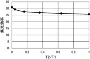
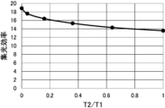
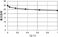
- FIG. 4 is a graph showing light collection efficiency in an example of the present invention.
- FIG. 5 is a graph showing light collection efficiency in an example of the present invention.
- FIG. 6 is a graph showing light collection efficiency in an example of the present invention.
- FIG. 7 is a graph showing light collection efficiency in an example of the present invention.
- FIG. 8 is a graph showing light collection efficiency in an example of the present invention.
- FIG. 9 is a graph showing light collection efficiency in an example of the present invention.
- FIG. 10 is a graph showing light collection efficiency in an example of the present invention.
- FIG. 11 is a graph showing light collection efficiency in an example of the present invention.
- a numerical range expressed using “ ⁇ ” means a range that includes the numerical values written before and after “ ⁇ ” as lower and upper limits.
- “same” includes a generally accepted error range in the technical field.
- FIGS. 1 and 2 conceptually show an example of the metalens of the present invention.
- FIG. 1 is a front view of the metalens 10
- FIG. 2 is a side view of the metalens 10.
- a front view is a view of the metalens viewed from the light incident direction, that is, the optical axis direction
- a side view is a view of the metalens viewed from a direction orthogonal to the front view.
- the shape of each part in the front view is also referred to as a "planar shape.”
- the metalens 10 of the present invention has a first region 12 and a second region 14.
- the first region 12 is a region in which a plurality of microstructures 20 are arranged to diffract and condense terahertz waves.
- the second region 14 is a region surrounding the first region 12 and is different from the first region 12.
- the metalens 10 of the illustrated example has a first region 12 in which a plurality of microstructures 20 are arranged (arranged) in the center of the surface of one base material 16, and a second region 12 on the outside of the first region 12 on the base material 16. area 14.
- the boundary between the first region 12 and the second region 14 in the base material 16 is shown by a dashed line.
- the boundary between the first region 12 and the second region 14 may be clearly visible.
- the boundary between the first region 12 and the second region 14 is not necessarily clearly shown on the base material 16.
- the wavelength with the highest light collection efficiency is the wavelength X
- the transmittance of the terahertz wave with the wavelength X in the first region 12 is the transmittance T1
- the transmittance of the terahertz wave with the wavelength X in the second region 14 is the transmittance T2
- the transmittance T2 is lower than the transmittance T1.
- terahertz waves are electromagnetic waves with a frequency of 0.1 to 10 THz, that is, electromagnetic waves with a wavelength of 0.3 to 3 mm.
- the base material 16 there is no restriction on the base material 16, and any known sheet-like material (film , plates, layers) are available.
- the base material 16 various sheet-like materials made of materials with high transmittance of metahertz waves can be used. Examples include sheet materials made of resin materials such as cycloolefin polymers (COP) and polyimide, and sheet materials made of inorganic materials such as glass and silicon.
- the base material 16 made of COP which has a high transmittance of metahertz waves, is preferably used.
- the thickness of the base material 16 there is no limit to the thickness of the base material 16, and the thickness that can support the microstructure 20 and ensure sufficient metahertz wave transmittance in the first region 12 can be determined depending on the material for forming the base material 16. , may be set as appropriate.
- the first region 12 has a plurality of fine structures 20 arranged therein and diffracts and focuses terahertz waves.
- the first region 12 is a region in which the refractive index, that is, the rate of change in phase given to the transmitted terahertz wave, gradually changes from the center toward the outside.
- the first region 12 is the smallest circular region that inscribes a group of microstructures 20 that have the function of diffracting and focusing terahertz waves, as shown by the dashed line in FIG. . That is, in the metalens of the present invention, the planar shape of the first region 12 is circular.
- the first region 12 is basically similar to a known metalens, that is, a condensing element made of a metasurface structure, and refracts (diffracts) the transmitted light by phase modulation. Focus light. That is, the first region 12 is formed by two-dimensionally arranging the microstructures 20 on the base material 16 at a distance, and basically includes one microstructure 20 and the microstructures. It is constituted by an arrangement of unit cells formed by the space around the body 20. Like a known metalens, the first region 12 modulates the phase of the transmitted light by using the resonance of the fine structure 20 by arranging unit cells, and uses Huygens' principle by phase modulation. It refracts and focuses the light accordingly. In the following description, the fine structure 20 is also referred to as a resonator 20.
- the first region 12 is basically a metalens made of a known metasurface structure (metamaterial). Therefore, there are no restrictions on the shape and forming material of the resonators 20, the arrangement of the resonators 20, the interval (pitch) between the resonators 20, etc. That is, the first region 12 may be designed by a known method depending on the desired light condensing characteristics.
- ⁇ is the wavelength of the incident terahertz wave
- r is the distance from the center of the lens
- F is the designed focal position
- ⁇ 0 is the transmission phase at the center of the lens.
- Structures that can be used in the first region 12 include the metal pattern structure described in the above-mentioned Non-Patent Document 1 (Vol. 29, No. 12/7 June 2021/Optics Express 18988), and the metal pattern structure described in “Vol. 26, The dielectric pattern structure described in "No. 23
- the number of resonators 20 that one unit cell has is basically one, but the present invention is not limited to this. That is, in the metalens of the present invention, one unit cell may be formed into a plurality of cells as necessary depending on the desired optical properties, the size, forming material and shape of the resonator 20, and the size of the unit cell. It may have a resonator 20 of. However, when one unit cell has a plurality of resonators 20, basically the amount of phase modulation in the space where each resonator of the unit cell exists is equal.
- the material for forming the resonator 20 constituting the first region 12 is not limited, and may be used as a resonator (fine structure) in a known metalens (metasurface structure).
- Various types are available.
- materials forming the resonator 20 in the first region 12 include metals and dielectrics. In the case of metals, copper, gold, and silver are preferred examples because of their low optical loss.
- dielectric materials silicon, titanium oxide, and germanium are preferably exemplified because they have a large refractive index and can perform large phase modulation.
- the shape of the resonator 20 constituting the first region 12 there is no limit to the shape of the resonator 20 constituting the first region 12, and various shapes used as resonators in known metalens (metasurface structures) can be used. Examples include a plate shape (rectangular parallelepiped shape) as shown in FIGS. 1 and 2, a metal wire (metal thread) as described in Non-Patent Document 1, a cylindrical shape, as shown in Japanese Patent Application Laid-open No. 2018-46395.
- a solid body with a V-shaped bottom surface and a solid body with a cross-shaped bottom surface can be used in various shapes by adjusting the angle formed by two rectangular parallelepipeds. It is possible.
- solid objects with the bottom shape as shown in Figure 5 of “Appl. Sci. 2018, 8(9), 1689; https://doi.org/10.3390/app8091689” can also be used. It is.
- the directions of the same resonators 20 may be the same or different as shown in FIG. 1, or there may be a mixture of resonators 20 in the same direction and those in different directions.
- the structure in which the resonators 20 are arranged in this manner that is, the arrangement structure of the resonators 20 is not limited to one layer, but may be two layers, or three or more layers. Further, the first region 12 may have a structure in which resonators 20 are arranged on both sides of the base material 16, like a metalens shown in Non-Patent Document 1.
- the metalens 10 of the present invention surrounds such a first region 12 and has a second region 14 that is a different region from the first region 12 . Further, the metalens 10 of the present invention has a terahertz wave with a wavelength of 0.3 mm, a wavelength of 1 mm, and a wavelength of 3 mm, and when the wavelength with the highest light collection efficiency is the wavelength X, as shown in FIG.
- the transmittance T2 which is the transmittance of the terahertz wave with the wavelength X in the second region 14, is lower than the transmittance T1, which is the transmittance of the terahertz wave with the wavelength X in the first region 12.
- transmittance T1 that is the transmittance of the terahertz wave of wavelength X in the first region 12
- T2 that is the transmittance of the terahertz wave of wavelength X in the second region 14
- the metalens 10 of the present invention can condense the terahertz wave with high condensing efficiency when the terahertz wave is incident.
- a metalens that collects terahertz waves has a lower light collection efficiency than a normal lens made of glass or the like that collects visible light.
- ordinary lenses such as glass lenses are also referred to as “optical lenses” for convenience in order to distinguish them from metalens.
- the inventors of the present invention have extensively studied the reason for this. As a result, they found that in a metalens that collects terahertz waves, the light collection efficiency decreases due to the wraparound of light (terahertz waves) from around the metalens.
- Various types of lenses such as optical lenses and metalens, are usually surrounded by air.
- light electromagnétique waves
- the light is diffracted due to various factors such as the difference in refractive index and transmittance between the lens and air, resulting in an undesired result.
- This causes the light to travel in the appropriate direction.
- the light that is refracted by the lens and travels properly interferes with the wrapped light, weakening the intensity of the light that is focused at the focal point.As a result, the light collection efficiency decreases. decreases.
- Such light wraparound affects an area from the end of the lens to a region several times the wavelength of the incident light.
- the wavelength of the incident light is short compared to the size of the lens. That is, in an optical lens, the lens is sufficiently large relative to the wavelength of the light to be condensed.
- the wavelength of the focused light is extremely long compared to the size of the lens. That is, in a metalens compatible with terahertz waves, the lens is small compared to the wavelength of the light to be focused.
- the wavelength of visible light is about 700 nm at most. Therefore, even if light wraps around the lens to a range several times the wavelength, the range is only a few ⁇ m. Therefore, for example, if the diameter of a lens is 5 cm, the size of the lens is large enough to prevent light from entering the lens, so the influence of the light entering the lens is very small and can be ignored.
- terahertz waves have a much longer wavelength than visible light. For example, in the case of a terahertz wave with a wavelength of 1 mm, the amount of wraparound from the periphery of the lens is approximately several mm.
- the influence of terahertz waves coming from the surroundings is much greater than that of visible light. That is, in a metalens compatible with terahertz waves, the structure that diffracts light is small relative to the wavelength, so the influence of terahertz waves that wrap around the lens becomes very large. As a result, in a metalens that supports terahertz waves, the terahertz waves that have wrapped around the lens interfere with the properly traveling terahertz waves that have been refracted by the lens, reducing the amount of components that can be properly focused. As a result, the light collection efficiency becomes low.
- the present invention was achieved by obtaining such knowledge, and by focusing on the transmittance of terahertz waves around the metalens, the transmittance of terahertz waves around the metalens is made to be higher than the transmittance of the metalens. By lowering the amount of light, the light collection efficiency is improved. That is, as described above, the metalens 10 of the present invention has a second region that is different from the first region 12 and surrounds the first region 12 that acts as a metalens, and further has a second region that is different from the first region 12. The transmittance T2 of the second region 14 surrounding the first region 12 is lower than the transmittance T1. In other words, in the metalens 10 of the present invention, the transmittance of the target terahertz wave is lower in the second region 14, which is a surrounding region surrounding the first region 12, than in the first region 12, which acts as a metalens. .
- the metalens 10 of the present invention transmits the terahertz waves incident around the first region 12 that acts as a metalens to the third region surrounding the first region 12 and having a lower transmittance than the first region.
- the two regions 14 attenuate and preferably block light. Therefore, according to the metalens 10 of the present invention, it is possible to reduce the terahertz waves that wrap around the first region 12, thereby reducing the adverse effect on the properly traveling terahertz waves that are refracted (diffracted) in the first region 12. I can do it.
- the metalens 10 of the present invention when a terahertz wave is incident, the terahertz wave can be focused with high focusing efficiency.
- the light collection efficiency of a lens refers to the ratio of the maximum electric field strength at the light collection point formed behind the lens to the electric field strength of the plane wave when a plane wave is incident on the lens. shall be.
- the light collection efficiency of the metalens is measured as follows using an imaging detector capable of measuring the target terahertz wave.
- an imaging detector capable of measuring the target terahertz wave.
- an imaging detector is placed at a focal point formed behind the metalens.
- the terahertz wave is incident on the imaging detector via the metalens, and the maximum value of the electric field strength at the focal point is measured.
- the metalens may be removed, the intensity of the incident plane wave may be measured with an imaging detector at the same position as before, the average value thereof may be calculated, and the ratio of this value to the maximum value of the electric field intensity at the focal point may be calculated.
- the transmittance T1 of the first region 12 refers to the ratio of the intensity of a plane wave incident on the first region 12 to the electromagnetic wave transmitted through the first region 12.
- the transmittance T1 of the first region 12 is a transmittance including the resonator 20.
- the transmittance T2 of the second region 14 refers to the ratio of the intensity of a plane wave incident on the second region 14 to the electromagnetic wave transmitted through the second region 14.
- the transmittance T1 of the first region 12 and the transmittance T2 of the second region 14 are measured as follows using an imaging detector capable of photometric measurement of the target terahertz wave.
- a metalens is placed just in front of the imaging detector.
- the terahertz wave is incident on the imaging detector via the metalens, the intensity of the electromagnetic wave detected at the pixel corresponding to the first region 12 or the second region 14 is measured, and the average value is measured. do.
- This average value is defined as the transmitted intensity.
- the metalens is removed and the intensity of the incident plane wave is measured with an imaging detector at the same position as before, and the average value is calculated. This average value is taken as the incident plane wave intensity.
- the ratio "(transmission intensity/incident plane wave intensity) x 100)" between the measured transmitted intensity and the incident plane wave intensity is calculated and used as the transmittance in the first region 12 and the second region 14.
- the transmittance T2 of the second region 14 is lower than the transmittance T1 of the first region 12.
- the greater the difference between the transmittance T2 and the transmittance T1 the greater the effect of improving the light collection efficiency.
- the ratio of the transmittance T2 of the second region 14 to the transmittance T1 of the first region 12 satisfies "transmittance T2/transmittance T1 ⁇ 0.5" in the metalens 10. .
- the ratio between the transmittance T1 and the transmittance T2 is more preferably less than 0.3, further preferably less than 0.1, and most preferably 0. That is, in the present invention, it is most preferable that the transmittance T2 in the second region 14 is 0%.
- the transmittance T2 of the second region 14 is lower than the transmittance T1 of the first region 12. As long as this condition is met, there is no limit to the transmittance T2 of the second region 14, but it is preferable that the transmittance T2 is 10% or less. By setting the transmittance T2 to 10% or less, it is preferable that the terahertz waves that wrap around the first region 12 can be sufficiently reduced and the effect of improving light collection efficiency can be suitably obtained. Note that the transmittance T2 is more preferably 5% or less, further preferably 3% or less, and most preferably 0% as described above.
- the above-mentioned wavelength X [mm] and the diameter R1 [mm] of the first region 12 satisfy "R1/X ⁇ 25".
- the metalens 10 is preferable because it satisfies this condition and can effectively improve the light collection efficiency by increasing the difference between the transmittance T1 and the transmittance T2.
- the metalens 10 of the present invention more preferably satisfies "R1/X ⁇ 20", and even more preferably satisfies "R1/X ⁇ 15".
- the size of the second region 14 is not limited as long as it is provided surrounding the first region 12.
- the terahertz wave wraps around the first region 12 most often in the vicinity of the first region 12, which causes a decrease in light collection efficiency.
- the wraparound of the terahertz waves from the periphery of the first region 12 decreases as the distance from the first region 12 increases, and the light collection efficiency is no longer affected from a position separated to a certain extent.
- the size of the second region 14 is a size corresponding to a circle whose center coincides with the first region 12, and is preferably about 2 to 10 times the diameter R1 of the first region 12, and 2 to 5 times the diameter R1 of the first region 12. More preferably, it is about double that.
- the first region 12 is the resonator 20 (fine structure 20) that has the function of diffracting and focusing terahertz waves, as shown by the dashed line in FIG. is the region of the smallest circle that inscribes the group of . That is, in the metalens 10 of the present invention, the first region 12 that acts as a metalens has a circular planar shape.
- the second region 14 surrounding the first region 12 also has a circular planar shape (appearance). That is, the planar shape of the second region 14 is annular.
- the present invention is not limited to this, and if the second region surrounds the first region, its external planar shape can be various shapes such as polygons such as quadrangles and hexagons, ellipses, irregular shapes, etc. shapes are available.
- the second region 14 can be formed by various known methods as long as the transmittance T2 is lower than the transmittance T1 of the first region 12. Note that the reduction in transmittance of the terahertz wave in the second region 14, preferably shielding, may be performed by absorption or reflection.
- a method of forming a film that absorbs or reflects terahertz waves on the surface of the base material 16 corresponding to the second region 14 is exemplified.
- a method is exemplified in which a film is formed on the surface of the base material 16 corresponding to the second region 14 to block terahertz waves by absorption or reflection.
- films that absorb or reflect terahertz waves can be used as long as they absorb or reflect terahertz waves, such as films made of resin materials, metal films, and films made of magnetic materials.
- Films that absorb or reflect terahertz waves can be formed using known methods depending on the forming material, such as coating with paint, vacuum deposition, vapor phase film formation such as CVD (Chemical Vapor Deposition), or plating.
- CVD Chemical Vapor Deposition
- Another example is a method in which the forming material of the base material 16 is changed between the first region 12 and the second region 14. That is, in the first region 12, a base material with high transmittance of terahertz waves is used, and around this base material, the second region 14 is formed of a base material (sheet-like material) with low transmittance of terahertz waves. Then, the transmittance T2 of the second region 14 is made lower than the transmittance T1 of the first region 12.
- the transmittance T2 of the second region 14 is preferably uniform, but may be non-uniform. As described above, the amount of light that comes from around the first region 12 is greatest in the vicinity of the first region 12, and decreases as the distance from the first region 12 increases. Considering this point, when the transmittance T2 of the second region 14 is non-uniform, the transmittance T2 is lowest near the first region 12 and increases as the distance from the first region 12 increases. is preferable.
- the resonator 20 is provided only in the first region 12, but the present invention is not limited to this. That is, the metalens of the present invention may have the resonator 20 also in the second region 14, if necessary. However, when the second region 14 includes the resonator 20, the plurality of resonators 20, that is, the unit cells, do not diffract the terahertz wave, that is, do not have the function of condensing the terahertz wave.
- Example A A metalens was designed in which a circular first region is surrounded by an annular second region, as shown in FIG. 1, in which the first region has a diameter R1 of 31 mm and the second region has a diameter R2 of 62 mm.
- ⁇ is the wavelength of the incident terahertz wave
- r is the distance from the center of the lens
- F is the designed focal position
- ⁇ 0 is the transmission phase at the center of the lens.
- ⁇ is the wavelength with the highest light collection efficiency, and was designed to have a wavelength of 3 mm. That is, a terahertz wave with a wavelength of 3 mm and a frequency of 0.1 THz is assumed.
- the designed focal length F was 50 mm.
- Metalens of Examples A1 to A5 and Comparative Example A1 were produced by changing the transmittance T1 of the first region and the transmittance T2 of the second region variously.
- the transmittance T1 and the transmittance T2 were calculated by simulation by calculating the intensity of the electromagnetic wave immediately after passing through the lens, and by calculating the ratio of the electric field intensity of the incident plane wave.
- the transmittance T1 of the first region and the transmittance T2 of the second region are the transmittances normalized with the transmittance T1 of the first region being "1". Note that the transmittance T1 of the first region is 90%.
- the light collection efficiency (maximum electric field strength) at the light collection point was evaluated by simulation using the Fourier transform beam propagation method (FFT-BPM method). The results are shown in Table 1 and FIG. 4 below.
- Example B Metalens of Examples B1 to B5 and Comparative Example B1 were produced in the same manner as Example A, except that the focal length F was 75 mm, and the light collection efficiency was evaluated. The results are shown in Table 2 and FIG. 5 below.
- Example C Metalens of Examples C1 to C5 and Comparative Example C1 were produced in the same manner as Example A, except that the focal length F was 100 mm, and the light collection efficiency was evaluated. The results are shown in Table 3 and FIG. 6 below.
- Example D Metalens of Examples D1 to D5 and Comparative Example D1 were produced in the same manner as Example A, except that the focal length F was 150 mm, and the light collection efficiency was evaluated. The results are shown in Table 4 and FIG. 7 below.
- Example E The metalens of Examples E1 to E5 and Comparative Example E1 were produced in the same manner as Example A, except that the diameter R1 of the first region was 41 mm, the diameter R2 of the second region was 82 mm, and the focal length F was 150 mm. Then, the light collection efficiency was evaluated. The results are shown in Table 5 and FIG. 8 below.
- Example F The metalens of Examples F1 to F5 and Comparative Example F1 were produced in the same manner as Example A, except that the diameter R1 of the first region was 52 mm, the diameter R2 of the second region was 104 mm, and the focal length F was 150 mm. Then, the light collection efficiency was evaluated. The results are shown in Table 6 and FIG. 9 below.
- Example G The metalens of Examples G1 to G5 and Comparative Example G1 were produced in the same manner as Example A, except that the diameter R1 of the first region was 62 mm, the diameter R2 of the second region was 124 mm, and the focal length F was 150 mm. Then, the light collection efficiency was evaluated. The results are shown in Table 7 and FIG. 10 below.
- Example H The metalens of Examples H1 to H5 and Comparative Example H1 were produced in the same manner as Example A, except that the diameter R1 of the first region was 72 mm, the diameter R2 of the second region was 144 mm, and the focal length F was 150 mm. Then, the light collection efficiency was evaluated. The results are shown in Table 8 below and FIG. 11.
- the metalens of the present invention which has a ratio lower than T1, has a higher light collection efficiency than the comparative metalens that does not satisfy this condition.
- the smaller T2/T1 that is, the larger the difference between transmittance T2 and transmittance T1, the higher the light collection efficiency is obtained.
- the effect of improving the light collection efficiency is favorably obtained, and in the region where the transmittance T2 of the second region is 10% or less, the light collection efficiency is further improved.
- the improvement effect has been suitably obtained. Note that, as described above, since the transmittance T1 of the first region is 90%, the transmittance of the second region where the transmittance T2 is 0.11 or less is 10% or less. Furthermore, the larger the diameter R1 of the first region relative to the wavelength (3 mm) of the incident terahertz wave, that is, "R1/X", the higher the light collection efficiency becomes.
- metalens 12 first region 14 second region 16 base material 20 microstructure (resonator)
Landscapes
- Chemical & Material Sciences (AREA)
- Engineering & Computer Science (AREA)
- Nanotechnology (AREA)
- Physics & Mathematics (AREA)
- Crystallography & Structural Chemistry (AREA)
- Materials Engineering (AREA)
- General Physics & Mathematics (AREA)
- Condensed Matter Physics & Semiconductors (AREA)
- Composite Materials (AREA)
- Life Sciences & Earth Sciences (AREA)
- Biophysics (AREA)
- Optics & Photonics (AREA)
- Investigating Or Analysing Materials By Optical Means (AREA)
- Optical Modulation, Optical Deflection, Nonlinear Optics, Optical Demodulation, Optical Logic Elements (AREA)
Priority Applications (3)
| Application Number | Priority Date | Filing Date | Title |
|---|---|---|---|
| JP2024512251A JPWO2023189994A1 (https=) | 2022-03-29 | 2023-03-23 | |
| CN202380030767.6A CN118975055A (zh) | 2022-03-29 | 2023-03-23 | 超透镜 |
| US18/894,769 US12620686B2 (en) | 2022-03-29 | 2024-09-24 | Metalens |
Applications Claiming Priority (2)
| Application Number | Priority Date | Filing Date | Title |
|---|---|---|---|
| JP2022053533 | 2022-03-29 | ||
| JP2022-053533 | 2022-03-29 |
Related Child Applications (1)
| Application Number | Title | Priority Date | Filing Date |
|---|---|---|---|
| US18/894,769 Continuation US12620686B2 (en) | 2022-03-29 | 2024-09-24 | Metalens |
Publications (1)
| Publication Number | Publication Date |
|---|---|
| WO2023189994A1 true WO2023189994A1 (ja) | 2023-10-05 |
Family
ID=88201919
Family Applications (1)
| Application Number | Title | Priority Date | Filing Date |
|---|---|---|---|
| PCT/JP2023/011398 Ceased WO2023189994A1 (ja) | 2022-03-29 | 2023-03-23 | メタレンズ |
Country Status (3)
| Country | Link |
|---|---|
| JP (1) | JPWO2023189994A1 (https=) |
| CN (1) | CN118975055A (https=) |
| WO (1) | WO2023189994A1 (https=) |
Cited By (1)
| Publication number | Priority date | Publication date | Assignee | Title |
|---|---|---|---|---|
| WO2024161881A1 (ja) * | 2023-01-31 | 2024-08-08 | パナソニックIpマネジメント株式会社 | 光学レンズ |
Citations (5)
| Publication number | Priority date | Publication date | Assignee | Title |
|---|---|---|---|---|
| JP2009266900A (ja) * | 2008-04-22 | 2009-11-12 | Panasonic Corp | 固体撮像素子 |
| JP2011028132A (ja) * | 2009-07-28 | 2011-02-10 | Panasonic Corp | テラヘルツ波装置 |
| WO2014142294A1 (ja) * | 2013-03-15 | 2014-09-18 | 国立大学法人茨城大学 | メタルプレートレンズ |
| EP3179297A1 (en) * | 2015-12-09 | 2017-06-14 | Samsung Electronics Co., Ltd. | Meta device |
| JP2018529278A (ja) * | 2015-08-25 | 2018-10-04 | ホアウェイ・テクノロジーズ・カンパニー・リミテッド | マルチビームアンテナアレイアセンブリのためのメタマテリアルに基づくトランスミットアレイ |
-
2023
- 2023-03-23 WO PCT/JP2023/011398 patent/WO2023189994A1/ja not_active Ceased
- 2023-03-23 JP JP2024512251A patent/JPWO2023189994A1/ja active Pending
- 2023-03-23 CN CN202380030767.6A patent/CN118975055A/zh active Pending
Patent Citations (5)
| Publication number | Priority date | Publication date | Assignee | Title |
|---|---|---|---|---|
| JP2009266900A (ja) * | 2008-04-22 | 2009-11-12 | Panasonic Corp | 固体撮像素子 |
| JP2011028132A (ja) * | 2009-07-28 | 2011-02-10 | Panasonic Corp | テラヘルツ波装置 |
| WO2014142294A1 (ja) * | 2013-03-15 | 2014-09-18 | 国立大学法人茨城大学 | メタルプレートレンズ |
| JP2018529278A (ja) * | 2015-08-25 | 2018-10-04 | ホアウェイ・テクノロジーズ・カンパニー・リミテッド | マルチビームアンテナアレイアセンブリのためのメタマテリアルに基づくトランスミットアレイ |
| EP3179297A1 (en) * | 2015-12-09 | 2017-06-14 | Samsung Electronics Co., Ltd. | Meta device |
Cited By (1)
| Publication number | Priority date | Publication date | Assignee | Title |
|---|---|---|---|---|
| WO2024161881A1 (ja) * | 2023-01-31 | 2024-08-08 | パナソニックIpマネジメント株式会社 | 光学レンズ |
Also Published As
| Publication number | Publication date |
|---|---|
| JPWO2023189994A1 (https=) | 2023-10-05 |
| CN118975055A (zh) | 2024-11-15 |
| US20250015474A1 (en) | 2025-01-09 |
Similar Documents
| Publication | Publication Date | Title |
|---|---|---|
| JP7148747B2 (ja) | Ledからの発光をコリメートするためのナノ構造化されたメタマテリアルおよびメタサーフェス | |
| US11428929B2 (en) | Focusing device comprising a plurality of scatterers and beam scanner and scope device | |
| CN109669226B (zh) | 一种基于超表面透镜组阵列的激光雷达扫描装置及其设计方法 | |
| KR102429949B1 (ko) | 입사 전자기파들로부터 근거리 구역에서 필드 강도 패턴을 형성하기 위한 디바이스 | |
| US7408712B2 (en) | Polarization-selectively blazed, diffractive optical element | |
| CN111061070B (zh) | 基于超表面结构的多功能阵列元件及多功能实现方法 | |
| CN103119498B (zh) | 纳米光学的折射光学器件 | |
| US5138495A (en) | Diffractive optical lens | |
| US12174512B2 (en) | Device for forming an outgoing electromagnetic wave from an incident electromagnetic wave | |
| US20240012177A1 (en) | Self-Aligned Nano-Pillar Coatings and Method of Manufacturing | |
| CN105891609B (zh) | 一种热机械式电磁辐射探测器的制备方法 | |
| US20230221462A1 (en) | Metasurface optical device with tilted nano-structure units and optical apparatus | |
| JP2020522009A (ja) | 分散設計型の誘電性メタ表面による広帯域アクロマティック平坦光学コンポーネント | |
| KR102420017B1 (ko) | 광학필터 및 이를 포함하는 전자장치 | |
| US11378797B2 (en) | Focusing device comprising a plurality of scatterers and beam scanner and scope device | |
| US20250116801A1 (en) | Metasurface-based imaging system, design method, and detector | |
| David et al. | Wavelength tunable diffractive transmission lens for hard x rays | |
| US20240337777A1 (en) | Micro-lens based on high-refractive-index dielectric substrate | |
| WO2023189994A1 (ja) | メタレンズ | |
| CN117871969A (zh) | 一种结合里德堡原子天线和龙伯透镜的能量导入接收装置 | |
| TWI613424B (zh) | 用於在微機電系統熱輻射偵測計中增加紅外線吸收的裝置 | |
| CN116953923B (zh) | 一种超透镜设计方法及超透镜 | |
| US12620686B2 (en) | Metalens | |
| CN116300125A (zh) | 一种光子纳米喷射的微柱阵列、制备方法及光学系统 | |
| CN113514905A (zh) | 一种等离子体超表面标准具结构的相位调制器 |
Legal Events
| Date | Code | Title | Description |
|---|---|---|---|
| 121 | Ep: the epo has been informed by wipo that ep was designated in this application |
Ref document number: 23780005 Country of ref document: EP Kind code of ref document: A1 |
|
| ENP | Entry into the national phase |
Ref document number: 2024512251 Country of ref document: JP Kind code of ref document: A |
|
| WWE | Wipo information: entry into national phase |
Ref document number: 202380030767.6 Country of ref document: CN |
|
| NENP | Non-entry into the national phase |
Ref country code: DE |
|
| 122 | Ep: pct application non-entry in european phase |
Ref document number: 23780005 Country of ref document: EP Kind code of ref document: A1 |