WO2023188146A1 - レーザ素子及び電子機器 - Google Patents
レーザ素子及び電子機器 Download PDFInfo
- Publication number
- WO2023188146A1 WO2023188146A1 PCT/JP2022/016104 JP2022016104W WO2023188146A1 WO 2023188146 A1 WO2023188146 A1 WO 2023188146A1 JP 2022016104 W JP2022016104 W JP 2022016104W WO 2023188146 A1 WO2023188146 A1 WO 2023188146A1
- Authority
- WO
- WIPO (PCT)
- Prior art keywords
- light
- reflective layer
- laser
- wavelength
- layer
- Prior art date
- Legal status (The legal status is an assumption and is not a legal conclusion. Google has not performed a legal analysis and makes no representation as to the accuracy of the status listed.)
- Ceased
Links
Images







Classifications
-
- H—ELECTRICITY
- H01—ELECTRIC ELEMENTS
- H01S—DEVICES USING THE PROCESS OF LIGHT AMPLIFICATION BY STIMULATED EMISSION OF RADIATION [LASER] TO AMPLIFY OR GENERATE LIGHT; DEVICES USING STIMULATED EMISSION OF ELECTROMAGNETIC RADIATION IN WAVE RANGES OTHER THAN OPTICAL
- H01S5/00—Semiconductor lasers
- H01S5/10—Construction or shape of the optical resonator, e.g. extended or external cavity, coupled cavities, bent-guide, varying width, thickness or composition of the active region
- H01S5/18—Surface-emitting [SE] lasers, e.g. having both horizontal and vertical cavities
- H01S5/183—Surface-emitting [SE] lasers, e.g. having both horizontal and vertical cavities having only vertical cavities, e.g. vertical cavity surface-emitting lasers [VCSEL]
-
- H—ELECTRICITY
- H01—ELECTRIC ELEMENTS
- H01S—DEVICES USING THE PROCESS OF LIGHT AMPLIFICATION BY STIMULATED EMISSION OF RADIATION [LASER] TO AMPLIFY OR GENERATE LIGHT; DEVICES USING STIMULATED EMISSION OF ELECTROMAGNETIC RADIATION IN WAVE RANGES OTHER THAN OPTICAL
- H01S5/00—Semiconductor lasers
- H01S5/40—Arrangement of two or more semiconductor lasers, not provided for in groups H01S5/02 - H01S5/30
- H01S5/4012—Beam combining, e.g. by the use of fibres, gratings, polarisers, prisms
-
- H—ELECTRICITY
- H01—ELECTRIC ELEMENTS
- H01S—DEVICES USING THE PROCESS OF LIGHT AMPLIFICATION BY STIMULATED EMISSION OF RADIATION [LASER] TO AMPLIFY OR GENERATE LIGHT; DEVICES USING STIMULATED EMISSION OF ELECTROMAGNETIC RADIATION IN WAVE RANGES OTHER THAN OPTICAL
- H01S3/00—Lasers, i.e. devices using stimulated emission of electromagnetic radiation in the infrared, visible or ultraviolet wave range
- H01S3/05—Construction or shape of optical resonators; Accommodation of active medium therein; Shape of active medium
- H01S3/06—Construction or shape of active medium
- H01S3/0602—Crystal lasers or glass lasers
- H01S3/0612—Non-homogeneous structure
-
- H—ELECTRICITY
- H01—ELECTRIC ELEMENTS
- H01S—DEVICES USING THE PROCESS OF LIGHT AMPLIFICATION BY STIMULATED EMISSION OF RADIATION [LASER] TO AMPLIFY OR GENERATE LIGHT; DEVICES USING STIMULATED EMISSION OF ELECTROMAGNETIC RADIATION IN WAVE RANGES OTHER THAN OPTICAL
- H01S3/00—Lasers, i.e. devices using stimulated emission of electromagnetic radiation in the infrared, visible or ultraviolet wave range
- H01S3/05—Construction or shape of optical resonators; Accommodation of active medium therein; Shape of active medium
- H01S3/06—Construction or shape of active medium
- H01S3/0619—Coatings, e.g. AR, HR, passivation layer
- H01S3/0621—Coatings on the end-faces, e.g. input/output surfaces of the laser light
-
- H—ELECTRICITY
- H01—ELECTRIC ELEMENTS
- H01S—DEVICES USING THE PROCESS OF LIGHT AMPLIFICATION BY STIMULATED EMISSION OF RADIATION [LASER] TO AMPLIFY OR GENERATE LIGHT; DEVICES USING STIMULATED EMISSION OF ELECTROMAGNETIC RADIATION IN WAVE RANGES OTHER THAN OPTICAL
- H01S3/00—Lasers, i.e. devices using stimulated emission of electromagnetic radiation in the infrared, visible or ultraviolet wave range
- H01S3/05—Construction or shape of optical resonators; Accommodation of active medium therein; Shape of active medium
- H01S3/06—Construction or shape of active medium
- H01S3/0627—Construction or shape of active medium the resonator being monolithic, e.g. microlaser
-
- H—ELECTRICITY
- H01—ELECTRIC ELEMENTS
- H01S—DEVICES USING THE PROCESS OF LIGHT AMPLIFICATION BY STIMULATED EMISSION OF RADIATION [LASER] TO AMPLIFY OR GENERATE LIGHT; DEVICES USING STIMULATED EMISSION OF ELECTROMAGNETIC RADIATION IN WAVE RANGES OTHER THAN OPTICAL
- H01S3/00—Lasers, i.e. devices using stimulated emission of electromagnetic radiation in the infrared, visible or ultraviolet wave range
- H01S3/09—Processes or apparatus for excitation, e.g. pumping
- H01S3/091—Processes or apparatus for excitation, e.g. pumping using optical pumping
- H01S3/094—Processes or apparatus for excitation, e.g. pumping using optical pumping by coherent light
- H01S3/094073—Non-polarized pump, e.g. depolarizing the pump light for Raman lasers
-
- H—ELECTRICITY
- H01—ELECTRIC ELEMENTS
- H01S—DEVICES USING THE PROCESS OF LIGHT AMPLIFICATION BY STIMULATED EMISSION OF RADIATION [LASER] TO AMPLIFY OR GENERATE LIGHT; DEVICES USING STIMULATED EMISSION OF ELECTROMAGNETIC RADIATION IN WAVE RANGES OTHER THAN OPTICAL
- H01S3/00—Lasers, i.e. devices using stimulated emission of electromagnetic radiation in the infrared, visible or ultraviolet wave range
- H01S3/09—Processes or apparatus for excitation, e.g. pumping
- H01S3/091—Processes or apparatus for excitation, e.g. pumping using optical pumping
- H01S3/094—Processes or apparatus for excitation, e.g. pumping using optical pumping by coherent light
- H01S3/094084—Processes or apparatus for excitation, e.g. pumping using optical pumping by coherent light with pump light recycling, i.e. with reinjection of the unused pump light, e.g. by reflectors or circulators
-
- H—ELECTRICITY
- H01—ELECTRIC ELEMENTS
- H01S—DEVICES USING THE PROCESS OF LIGHT AMPLIFICATION BY STIMULATED EMISSION OF RADIATION [LASER] TO AMPLIFY OR GENERATE LIGHT; DEVICES USING STIMULATED EMISSION OF ELECTROMAGNETIC RADIATION IN WAVE RANGES OTHER THAN OPTICAL
- H01S3/00—Lasers, i.e. devices using stimulated emission of electromagnetic radiation in the infrared, visible or ultraviolet wave range
- H01S3/09—Processes or apparatus for excitation, e.g. pumping
- H01S3/091—Processes or apparatus for excitation, e.g. pumping using optical pumping
- H01S3/094—Processes or apparatus for excitation, e.g. pumping using optical pumping by coherent light
- H01S3/0941—Processes or apparatus for excitation, e.g. pumping using optical pumping by coherent light of a laser diode
- H01S3/09415—Processes or apparatus for excitation, e.g. pumping using optical pumping by coherent light of a laser diode the pumping beam being parallel to the lasing mode of the pumped medium, e.g. end-pumping
-
- H—ELECTRICITY
- H01—ELECTRIC ELEMENTS
- H01S—DEVICES USING THE PROCESS OF LIGHT AMPLIFICATION BY STIMULATED EMISSION OF RADIATION [LASER] TO AMPLIFY OR GENERATE LIGHT; DEVICES USING STIMULATED EMISSION OF ELECTROMAGNETIC RADIATION IN WAVE RANGES OTHER THAN OPTICAL
- H01S3/00—Lasers, i.e. devices using stimulated emission of electromagnetic radiation in the infrared, visible or ultraviolet wave range
- H01S3/10—Controlling the intensity, frequency, phase, polarisation or direction of the emitted radiation, e.g. switching, gating, modulating or demodulating
- H01S3/11—Mode locking; Q-switching; Other giant-pulse techniques, e.g. cavity dumping
- H01S3/1123—Q-switching
- H01S3/113—Q-switching using intracavity saturable absorbers
-
- H—ELECTRICITY
- H01—ELECTRIC ELEMENTS
- H01S—DEVICES USING THE PROCESS OF LIGHT AMPLIFICATION BY STIMULATED EMISSION OF RADIATION [LASER] TO AMPLIFY OR GENERATE LIGHT; DEVICES USING STIMULATED EMISSION OF ELECTROMAGNETIC RADIATION IN WAVE RANGES OTHER THAN OPTICAL
- H01S3/00—Lasers, i.e. devices using stimulated emission of electromagnetic radiation in the infrared, visible or ultraviolet wave range
- H01S3/14—Lasers, i.e. devices using stimulated emission of electromagnetic radiation in the infrared, visible or ultraviolet wave range characterised by the material used as the active medium
- H01S3/16—Solid materials
- H01S3/1601—Solid materials characterised by an active (lasing) ion
- H01S3/1603—Solid materials characterised by an active (lasing) ion rare earth
- H01S3/1611—Solid materials characterised by an active (lasing) ion rare earth neodymium
-
- H—ELECTRICITY
- H01—ELECTRIC ELEMENTS
- H01S—DEVICES USING THE PROCESS OF LIGHT AMPLIFICATION BY STIMULATED EMISSION OF RADIATION [LASER] TO AMPLIFY OR GENERATE LIGHT; DEVICES USING STIMULATED EMISSION OF ELECTROMAGNETIC RADIATION IN WAVE RANGES OTHER THAN OPTICAL
- H01S3/00—Lasers, i.e. devices using stimulated emission of electromagnetic radiation in the infrared, visible or ultraviolet wave range
- H01S3/14—Lasers, i.e. devices using stimulated emission of electromagnetic radiation in the infrared, visible or ultraviolet wave range characterised by the material used as the active medium
- H01S3/16—Solid materials
- H01S3/1601—Solid materials characterised by an active (lasing) ion
- H01S3/1603—Solid materials characterised by an active (lasing) ion rare earth
- H01S3/1618—Solid materials characterised by an active (lasing) ion rare earth ytterbium
-
- H—ELECTRICITY
- H01—ELECTRIC ELEMENTS
- H01S—DEVICES USING THE PROCESS OF LIGHT AMPLIFICATION BY STIMULATED EMISSION OF RADIATION [LASER] TO AMPLIFY OR GENERATE LIGHT; DEVICES USING STIMULATED EMISSION OF ELECTROMAGNETIC RADIATION IN WAVE RANGES OTHER THAN OPTICAL
- H01S5/00—Semiconductor lasers
- H01S5/10—Construction or shape of the optical resonator, e.g. extended or external cavity, coupled cavities, bent-guide, varying width, thickness or composition of the active region
- H01S5/14—External cavity lasers
- H01S5/141—External cavity lasers using a wavelength selective device, e.g. a grating or etalon
-
- H—ELECTRICITY
- H01—ELECTRIC ELEMENTS
- H01S—DEVICES USING THE PROCESS OF LIGHT AMPLIFICATION BY STIMULATED EMISSION OF RADIATION [LASER] TO AMPLIFY OR GENERATE LIGHT; DEVICES USING STIMULATED EMISSION OF ELECTROMAGNETIC RADIATION IN WAVE RANGES OTHER THAN OPTICAL
- H01S5/00—Semiconductor lasers
- H01S5/10—Construction or shape of the optical resonator, e.g. extended or external cavity, coupled cavities, bent-guide, varying width, thickness or composition of the active region
- H01S5/18—Surface-emitting [SE] lasers, e.g. having both horizontal and vertical cavities
- H01S5/183—Surface-emitting [SE] lasers, e.g. having both horizontal and vertical cavities having only vertical cavities, e.g. vertical cavity surface-emitting lasers [VCSEL]
- H01S5/18361—Structure of the reflectors, e.g. hybrid mirrors
-
- H—ELECTRICITY
- H01—ELECTRIC ELEMENTS
- H01S—DEVICES USING THE PROCESS OF LIGHT AMPLIFICATION BY STIMULATED EMISSION OF RADIATION [LASER] TO AMPLIFY OR GENERATE LIGHT; DEVICES USING STIMULATED EMISSION OF ELECTROMAGNETIC RADIATION IN WAVE RANGES OTHER THAN OPTICAL
- H01S3/00—Lasers, i.e. devices using stimulated emission of electromagnetic radiation in the infrared, visible or ultraviolet wave range
- H01S3/23—Arrangements of two or more lasers not provided for in groups H01S3/02 - H01S3/22, e.g. tandem arrangements of separate active media
- H01S3/2383—Parallel arrangements
-
- H—ELECTRICITY
- H01—ELECTRIC ELEMENTS
- H01S—DEVICES USING THE PROCESS OF LIGHT AMPLIFICATION BY STIMULATED EMISSION OF RADIATION [LASER] TO AMPLIFY OR GENERATE LIGHT; DEVICES USING STIMULATED EMISSION OF ELECTROMAGNETIC RADIATION IN WAVE RANGES OTHER THAN OPTICAL
- H01S5/00—Semiconductor lasers
- H01S5/40—Arrangement of two or more semiconductor lasers, not provided for in groups H01S5/02 - H01S5/30
- H01S5/42—Arrays of surface emitting lasers
- H01S5/423—Arrays of surface emitting lasers having a vertical cavity
Definitions
- the present disclosure relates to a laser device and an electronic device.
- Laser technology is applied in various fields such as microfabrication, medical equipment, and distance measurement.
- short-pulse laser technology is expected to be applied to high-precision processing technology or highly efficient wavelength conversion technology.
- Q-switched solid-state lasers are used in a wide range of application fields because they can obtain high peak powers exceeding kW (kilowatts) with a relatively simple configuration (see Patent Document 1).
- a multi-junction structure has been proposed in which a plurality of active layers are provided inside an excitation light source made of stacked semiconductor layers.
- This type of excitation light source has a higher thermal resistance than an EEL (Edge Emitting Laser), and has an upper limit (rollover point) of optical output. Therefore, when trying to increase the optical output by increasing the power of the excitation light source, the junction temperature increases and the long-term reliability (MTTF: Mean Time To Failure) of the device decreases.
- Patent Document 1 discloses a structure in which a solid-state laser medium for a Q switch is combined with a stacked semiconductor layer.
- a first resonator composed of a stacked semiconductor layer serving as an excitation light source and a solid-state laser medium, and a second resonator composed of a solid-state laser medium and a saturable absorber are adjacent to each other. This enables high-intensity excitation of solid-state laser media.
- the average output of the Q-switched light can be increased by spatially combining it using an optical lens or by combining it using polarized light.
- the waveform of the Q-switched light oscillated by the excitation light source includes jitter, and even if it is combined, the total peak power cannot be improved.
- the upper limit of the peak intensity of the Q-switched light is determined by the limit of the pumping light output for the reasons described above.
- the present disclosure provides a laser element and an electronic device that can improve the excitation light output without generating heat or reducing the lifespan.
- a stacked semiconductor layer includes a first reflective layer for light of a first wavelength, and an active layer that performs surface emission of the first wavelength; a second reflective layer for light of the first wavelength, which is disposed closer to the light exit surface than the laminated semiconductor layer; a polarization splitting element that individually resonates and combines orthogonally polarized lights included in the light emitted from the laminated semiconductor layer between the first reflective layer and the second reflective layer; A laser device is provided.
- the laminated semiconductor layer has a plurality of laminated semiconductor regions corresponding to the orthogonal polarized light
- the polarized light splitting element may individually resonate and combine the corresponding polarized light between the first reflective layer and the second reflective layer for each of the plurality of laminated semiconductor regions.
- the polarization splitting element includes a first surface that is in contact with the light exit surface of the laminated semiconductor layer, and a first surface that is disposed between the first reflective layer and the second reflective layer on the opposite side of the first surface. It may have two sides.
- the orthogonally polarized lights include orthogonally polarized lights of different wavelengths
- the polarization separation element may individually resonate and combine each of the orthogonally polarized lights, including orthogonally polarized lights of different wavelengths, between the first reflective layer and the second reflective layer.
- the orthogonal polarized light includes TM (Transverse Magnetic) polarized light and TE (Transverse Electric) polarized light
- the polarization separation element may individually resonate and combine the TE polarized light and the TM polarized light between the first reflective layer and the second reflective layer.
- the polarization splitting element may combine the TE polarized light with the TM polarized light inside the polarization splitting element.
- the polarization separation element has a laminate in which a plurality of polarization separation films and a plurality of reflection films are alternately stacked at intervals,
- the laminate has a cut surface cut in a direction of 45 degrees with respect to the normal direction of the laminate surface,
- the polarization splitting element may be arranged such that the normal direction of the cut plane is parallel to the normal direction of the laminated semiconductor layer.
- the polarization separation element may include a birefringent material that separates the light emitted from the laminated semiconductor layer into the orthogonal polarized light.
- a laser medium may be provided that is disposed closer to the light exit surface than the polarization splitting element and resonates at a second wavelength different from the first wavelength.
- a third reflective layer disposed on a first end face of the laser medium on the polarization splitting element side, and for light of the second wavelength;
- a fourth reflective layer for light of the second wavelength may be provided on a second end surface of the laser medium opposite to the first end surface.
- the third reflective layer may be placed closer to the light exit surface than the second reflective layer.
- the third reflective layer may be disposed between the polarization splitting element and the second reflective layer.
- the third reflective layer may be in contact with an end surface of the polarization splitting element.
- the fourth reflective layer may be in contact with the second reflective layer, or may be placed closer to the light exit surface than the second reflective layer.
- a saturable absorber may be provided that is placed closer to the light exit surface than the laser medium.
- a third reflective layer for light of the second wavelength which is disposed on the end face of the laser medium on the side facing the polarization splitting element;
- a fourth reflective layer for light of the second wavelength may be provided, which is disposed on the light exit surface side of the saturable absorber.
- the third reflective layer may be placed closer to the light exit surface than the second reflective layer.
- the second reflective layer may be disposed between the third reflective layer and the fourth reflective layer.
- Each of the laminated semiconductor layer, the polarized light splitting element, the laser medium, and the saturable absorber is arranged in correspondence with a plurality of light emitting parts arranged at predetermined intervals and emitting pulsed laser light of the second wavelength. , may be divided into multiple areas.
- a laser element comprising: a control unit that controls emitting light from the laser element;
- the laser element is a laminated semiconductor layer having a first reflective layer for light of a first wavelength and an active layer that performs surface emission of the first wavelength; a second reflective layer for light of the first wavelength, which is disposed closer to the light exit surface than the laminated semiconductor layer; a polarization splitting element that individually resonates and combines each of the plurality of polarized lights included in the light emitted from the laminated semiconductor layer between the first reflective layer and the second reflective layer; Electronic equipment provided.
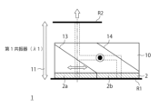
- FIG. 1 is a schematic cross-sectional view of a laser element according to a first embodiment.
- FIG. 2 is a schematic cross-sectional view and a plan view of a laser element according to a comparative example as seen from the light-emitting surface side.
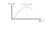
- 3 is a diagram showing the relationship between the current of the excitation light source and the optical output in the laser element of FIG. 2.
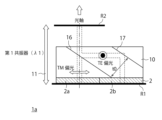
- FIG. 3 is a schematic cross-sectional view of a laser element according to a second embodiment.
- FIG. 3 is a diagram schematically showing a method for manufacturing a polarization splitting element.
- FIG. 3 is a diagram showing an example in which TM polarized light and TE polarized light are combined at approximately the center in the thickness direction of a polarization separation element.
- FIG. 1 is a schematic cross-sectional view of a laser element according to a first embodiment.
- FIG. 2 is a schematic cross-sectional view and a plan view of a laser element according to a comparative example as seen
- FIG. 7 is a schematic cross-sectional view of a laser element according to a third embodiment.
- FIG. 3 is a diagram showing a design example of a polarization separation film.
- FIG. 7 is a schematic cross-sectional view of a laser element according to a fourth embodiment.
- FIG. 7 is a schematic cross-sectional view of a laser element according to a fifth embodiment.
- FIG. 7 is a schematic cross-sectional view of a laser element according to a sixth embodiment.
- FIG. 7 is a schematic cross-sectional view of a laser element according to a seventh embodiment.
- FIG. 7 is a schematic cross-sectional view of a laser element according to an eighth embodiment.
- FIG. 14 is a schematic cross-sectional view showing each layer of the laser device of FIG. 13 in more detail.
- FIG. 1 is a cross-sectional view of a laser amplification element according to the present disclosure.
- FIG. 1 is a perspective view of a laser amplification element according to the present disclosure.
- FIG. 3 is a plan view schematically showing an optical path of a laser beam within a laser amplification element.
- FIG. 1 is a diagram showing an example of a schematic configuration of an endoscope system.
- 18 is a block diagram showing an example of the functional configuration of the camera and CCU shown in FIG. 17.
- FIG. FIG. 1 is a diagram illustrating an example of a schematic configuration of a microsurgery system.
- FIG. 1 is a schematic cross-sectional view of a laser device 1 according to the first embodiment.
- the laser device 1 according to the first embodiment includes an excitation light source 2 having a first reflective layer R1 and an active layer, a second reflective layer R2, and a polarization separation element 10. .
- the laser element 1 according to the first embodiment is an integrated layered structure that can be manufactured using semiconductor process technology, it has excellent mass productivity and excellent stability of laser output.
- the excitation light source 2 is a stacked semiconductor layer.
- the excitation light source 2 may be referred to as the laminated semiconductor layer 2.
- the laminated semiconductor layer 2 is a form of a vertical cavity surface emitting laser (VCSEL).
- VCSEL vertical cavity surface emitting laser
- the difference from a VCSEL is that the second reflective layer R2, which is at least one of the mirrors constituting the resonator, is provided outside the laminated semiconductor layer 2, which is the main body of the excitation light source 2.
- the second reflective layer R2 is, for example, an external cavity mirror.
- the stacked semiconductor layer 2 is also called a VECSEL (Vertical External-Cavity Surface Emitting Laser).
- the laminated semiconductor layer 2 has a first reflective layer R1 for light with a first wavelength ⁇ 1, and an active layer that performs surface emission with a first wavelength ⁇ 1.
- the detailed layer structure of the laminated semiconductor layer 2 will be described later.
- the second reflective layer R2 is arranged closer to the light emitting surface than the laminated semiconductor layer 2 is.
- a first resonator 11 that resonates light with a first wavelength ⁇ 1 is configured by the first reflective layer R1 and the second reflective layer R2.
- the polarization separation element 10 is a flat element that polarizes and separates the light from the excitation light source 2 provided between the first resonators 11.
- the polarization separation element 10 combines orthogonal polarized lights while uniquely determining the polarization direction. That is, the polarization separation element 10 separates each orthogonal polarized light included in the light emitted from the laminated semiconductor layer 2 constituting the excitation light source 2 between the first reflective layer R1 and the second reflective layer R2. Make it resonate and combine the waves.
- the internal structure of the polarization separation element 10 does not matter.
- a specific example of the polarization splitter 10 is a PBS (Polarizing Beam Splitter).
- the polarization separation element 10 by providing inside the polarization separation element 10 a first optical member 13 that transmits the first polarized light and reflects the second polarized light, and a second optical member 14 that reflects the second polarized light,
- the first polarized light is transmitted through the first optical member 13 and performs resonance operation between the first reflective layer R1 and the second reflective layer R2, and the second polarized light is transmitted through the second optical member 14 and the first optical member 13.
- the reflected light causes a resonance operation between the first reflective layer R1 and the second reflective layer R2.
- the polarization separation element 10 has a first surface that is in contact with the light exit surface of the laminated semiconductor layer 2, and a second surface that is disposed between the first reflective layer and the second reflective layer on the opposite side of the first surface. has.
- FIG. 2 is a schematic cross-sectional view of a laser element 100 according to a comparative example and a plan view seen from the light emitting surface side.
- the laser device 100 in FIG. 2 has a configuration in which an excitation light source 2 made of a laminated semiconductor layer 2, a Q-switch solid laser medium 3, and a saturable absorber 4 are arranged in this order.
- a uniform material layer 15 that does not control polarization may be arranged between the excitation light source 2 and the solid-state laser medium 3.
- This material layer 15 may be, for example, a support substrate that supports the excitation light source 2.
- the laser element 100 in FIG. 2 includes a first resonator 11 that resonates at a first wavelength ⁇ 1 and a second resonator 12 that resonates at a second wavelength ⁇ 2.
- the second resonator 12 is also called a Q-switch solid state laser resonator.
- the solid-state laser medium 3 in FIG. 2 is used in both the first resonator 11 and the second resonator 12.
- the first resonator 11 performs a resonant operation between the excitation light source 2 and the solid-state laser medium 3
- the second resonator 12 performs a resonant operation between the solid-state laser medium 3 and the saturable absorber 4.
- the solid laser medium 3 is excited by the light of the first wavelength ⁇ 1 emitted from the excitation light source 2 and resonated by the first resonator 11.
- the power of the excitation light with the first wavelength ⁇ 1 is accumulated in the solid-state laser medium 3 and the solid-state laser medium 3 reaches a sufficiently excited state, the light absorption rate in the saturable absorber 4 decreases rapidly, causing a second resonance.
- the device 12 causes light of the second wavelength ⁇ 2 to resonate between the third reflective layer and the fourth reflective layer, and a Q-switched laser pulse is emitted from the saturable absorber 4.
- FIG. 2 shows an example in which the light emitting section 20 has a circular shape.
- the excitation light source 2 in FIG. 2 is composed of the laminated semiconductor layers 2, the volume of the active layer in the laminated semiconductor layers 2 is limited. A multi-junction structure in which a plurality of active layers are provided in the laminated semiconductor layer 2 has also been proposed, but the excitation light source 2 shown in FIG. Unable to increase output. If an attempt is made to increase the optical output by increasing the power of the excitation light source 2, the junction temperature will rise and the life of the laser element 1 will be significantly reduced.
- FIG. 3 is a diagram showing the relationship between the current of the excitation light source 2 and the optical output in the laser element 100 of FIG. 2. As shown in FIG. 3, when the current flowing through the excitation light source 2 reaches a predetermined value, the optical output reaches its upper limit, and if the current is passed beyond that, the junction temperature rises and the optical output decreases.
- the first resonator 11 performs a resonance operation randomly regardless of the type of polarized light. Only light energy is transmitted from the first resonator 11 to the second resonator 12 without selecting a specific polarization.
- the laser element 1 is then divided into a plurality of laminated semiconductor regions.
- the plurality of stacked semiconductor regions emit unpolarized spontaneously emitted light.
- the polarization separation element 10 individually resonates and combines the corresponding polarized light between the first reflective layer R1 and the second reflective layer R2 for each of the plurality of laminated semiconductor regions.
- each of the two types of polarized light performs resonance operation individually between the first reflective layer R1 and the second reflective layer R2, so that The emitted light output can be approximately twice that of FIG.
- Being able to improve the optical output emitted from the polarization separation element 10 means that even if the current flowing through the excitation light source 2 is reduced compared to the laser element 100 of FIG. 2, the optical output can be maintained high. Since the flowing current can be lowered, the life of the laser element 1 can be extended.
- the laser element 1 in FIG. 1 can be made into an integrally bonded structure using a semiconductor process. Therefore, mass productivity can be improved, pump light from multiple stacked semiconductor regions can be combined to increase pump light output, and long-term reliability (MTTF: Mean Time To Failure) of the laser element 1 can be improved. You can improve.
- MTTF Mean Time To Failure
- each of the orthogonally polarized lights included in the light emitted from the laminated semiconductor layer 2 is resonated between the first reflective layer R1 and the second reflective layer R2 and combined. Therefore, the excitation light output can be increased without increasing the current flowing through the excitation light source 2.
- the excitation light source 2 is, for example, a semiconductor laser.
- the polarized light splitting element 10 is stacked inside the first resonator 11 using a semiconductor laser, and each polarized light beam separated in the polarized light splitting element 10 is combined, so even though the laser element 1 is small, it can excite Light output can be improved. Further, even if the current flowing through the excitation light source 2 is reduced, the excitation light output can be maintained high, so that the life of the laser element 1 can be extended.
- FIG. 4 is a schematic cross-sectional view of a laser element 1a according to the second embodiment.
- the orthogonally polarized light included in the light emitted from the laminated semiconductor layer 2 includes TM (Transverse Magnetic) polarized light and TE (Transverse Electric) polarized light.
- the polarization separation element 10 causes each of the TE polarized light and the TM polarized light to resonate and combine them between the first reflective layer R1 and the second reflective layer R2.
- a polarization conversion element can be considered as an example of the polarization separation element 10.
- the polarization conversion element can be manufactured using the same manufacturing method as that commonly used in liquid crystal projectors.
- a polarization conversion element for a liquid crystal projector has an aperture window disposed on the incident plane and a half-wave plate disposed on the output plane, but the polarization conversion element according to this embodiment does not require the aperture window and the half-wave plate. Instead, a polarization separation film 16 is placed on the combining surface.
- the polarization separation element 10 has a configuration in which polarization separation films 16 and reflective films 17, which are arranged in a direction inclined at 45 degrees with respect to the normal direction of the light entrance surface, are alternately arranged along the light entrance surface.
- the polarization separation film 16 has a property of transmitting TM polarized light but reflecting TE polarized light.
- the reflective film 17 has the property of reflecting TE polarized light. Therefore, by arranging the polarization separation film 16 and the reflection film 17 next to each other along the light incident surface, the TM polarized light is separated from the first reflection layer R1 and the second reflection layer R1 along the normal direction of the end surface of the polarization separation element 10. Resonance occurs between the reflective layers R2.
- the TE polarized light resonates between the first reflective layer R1 and the second reflective layer R2 while being reflected by the reflective film 17 and the polarization separation film 16.
- the TE polarized light is reflected by the reflective film 17, and when further reflected by the polarization separation film 16, it is combined with the TM polarized light. Thereby, the excitation light output output from the polarization separation film 16 can be increased.
- TM polarized light and TE polarized light can be combined.
- FIG. 5 is a diagram schematically showing a method for manufacturing the polarization splitting element 10.
- a laminate 25 is formed by alternately laminating a first substrate 22 in which a polarization separation film 16 is formed on the end face of a base material layer 21 and a second substrate 24 in which a reflective film 17 is formed on an end face of a base material layer 23.
- the materials of the base layers 21 and 23 are not particularly limited, but they must be materials that do not have a polarization separation function.
- the laminate 25 is cut at an inclination angle of 45 degrees with respect to the normal direction of the substrate surface, as shown by the two-dot chain line in FIG. 10 is prepared.
- the optical axes of the combined light will coincide. Even if a positional shift occurs in the direction of the substrate surface during bonding, it has robustness that does not cause a shift in the optical path of the polarized light splitting element 10 to be manufactured.
- FIG. 6A shows an example in which TM polarized light and TE polarized light are combined at approximately the center of the polarization separation element 10 in the thickness direction
- FIG. 3 is a diagram showing an example in which TE polarized light is combined.
- the combining positions of the TM polarized light and the TE polarized light are different due to the misalignment of the polarized light separating film 16 and the reflective film 17 in the substrate surface direction in the polarized light separating element 10, but after combining The optical paths of the TM polarized light and the TE polarized light are not shifted. Therefore, robustness can be improved.
- the polarization separation element has polarization separation films 16 and reflection films 17 arranged in a direction inclined at 45 degrees from the normal direction of the substrate surface, which are arranged alternately along the light incident surface.
- the TM polarized light and the TE polarized light included in the excitation light can be combined inside the polarization separation element 10, and the output of the excitation light can be increased.
- FIG. 7 is a schematic cross-sectional view of a laser element 1b according to the third embodiment.
- the laser device 1b in FIG. 7 is different from the laser devices 1 and 1a according to the first and second embodiments in the internal structure of the polarization separation element 10.
- the polarization separation element 10 includes a polarization separation film 16 and a plurality of reflective films 17a and 17b.
- the plurality of reflective films 1717a and 17b reflect TE polarized light of different wavelengths, respectively.
- the polarization separation element 10 in FIG. 7 includes a polarization separation film 16, a first reflection film 17a that reflects TE polarized light of wavelength ⁇ 1, and a second reflection film 17b that reflects TE polarized light of wavelength ⁇ 2.
- FIG. 8 is a diagram showing a design example of the polarization separation film 16, in which the horizontal axis represents wavelength and the vertical axis represents transmittance.
- FIG. 9 is a schematic cross-sectional view of a laser element 1c according to the fourth embodiment.
- the laser elements 1a and 1b in FIGS. 4 and 7 have a polarization separation element 10 in which polarization separation films 16 and reflective films 17 are arranged alternately, whereas the laser element 1c in FIG. 9 is made of a birefringent material. It has a polarization splitting element 10 as follows.
- a birefringent material is a material that separates incident light into orthogonal polarized light depending on the polarization state. Birefringent materials typically separate incident light into two polarized beams. One of the two polarized lights is called normal light (ordinary light), and the other is called extraordinary light.
- FIG. 9 shows an example in which, of two polarized lights separated by a birefringent material, TM polarized light is normal light and TE polarized light is extraordinary light.
- the TM polarized light performs resonance operation between the first reflective layer R1 and the second reflective layer R2 along the normal direction of the substrate surface.
- the TE polarized light travels obliquely within the birefringent material, is combined with the TM polarized light, and performs a resonant operation between the first reflective layer R1 and the second reflective layer R2.
- birefringent material examples include rutile, which is a titanium dioxide (TiO2) crystal, yttrium vanadate (YVO4) crystal, lithium niobate (LiNbO3) crystal, and quartz. Note that the specific type of birefringent material does not matter. It is desirable to use a material that has high transmittance for the wavelength of the excitation light emitted from the excitation light source 2 and is highly processable so as to achieve accuracy in the C-axis direction.
- Rutile crystal is a birefringent material with high birefringence, and the transmitted light can be separated into ordinary light and extraordinary light.
- the polarization state of extraordinary light is orthogonal to the polarization state of ordinary light.
- the polarization splitting element 10 is formed of a birefringent material, the internal structure of the polarization splitting element 10 can be simplified, and the manufacturing process can also be simplified.
- the manufacturing process can also be simplified.
- FIG. 10 is a schematic cross-sectional view of a laser element 1d according to the fifth embodiment.
- a laser device 1d in FIG. 10 has a configuration in which a solid laser medium 3 is provided in a laser device 1, 1a, 1b, or 1c according to any of the first to fourth embodiments.
- the solid-state laser medium 3 in FIG. 10 is arranged closer to the light exit surface than the polarization splitting element 10 is.
- the solid-state laser medium 3 is arranged closer to the light output surface than the second reflective layer R2.
- the solid-state laser medium 3 resonates at a second wavelength ⁇ 2 different from the first wavelength ⁇ 1.
- the solid-state laser medium 3 has a third reflective layer R3 disposed on the first end face, and a fourth reflective layer R4 disposed on the second end face opposite to the first end face.
- the third reflective layer R3 and the fourth reflective layer R4 reflect light of the second wavelength ⁇ 2. Therefore, the light having the second wavelength ⁇ 2 resonates between the third reflective layer R3 and the fourth reflective layer R4.
- the solid-state laser medium 3 includes, for example, YAG (yttrium aluminum garnet) crystal Yb:YAG doped with Yb (yttribium).
- YAG yttrium aluminum garnet
- Yb yttribium
- the first wavelength ⁇ 1 of the first resonator 11 is 940 nm
- the second wavelength ⁇ 2 of the second resonator 12 is 1030 nm.
- the solid-state laser medium 3 is not limited to Yb:YAG, and examples of the solid-state laser medium 3 include Nd:YAG, Nd:YVO4, Nd:YLF, Nd:glass, Yb:YAG, Yb:YLF, Yb:FAP, and Yb. At least one of the following materials can be used: SFAP, Yb:YVO, Yb:glass, Yb:KYW, Yb:BCBF, Yb:YCOB, Yb:GdCOB, and YB:YAB.
- the form is not limited to crystal, and does not hinder the use of ceramic materials.
- the solid-state laser medium 3 may be a four-level solid-state laser medium 3 or a quasi-three-level solid-state laser medium 3.
- first wavelength ⁇ 1 the appropriate excitation wavelength
- the solid laser medium 3 is arranged closer to the light output surface than the polarization splitting element 10, the wavelength of the emitted light can be converted. Since the laser element 1d according to the fifth embodiment can also be formed by a semiconductor process, mass productivity can be improved.
- the laser element according to the sixth embodiment is one in which a saturable absorber is provided closer to the light emitting surface than the solid laser medium 3.
- FIG. 11 is a schematic cross-sectional view of a laser element 1e according to the sixth embodiment.
- a laser device 1e in FIG. 11 has a configuration in which a solid laser medium 3 and a saturable absorber 4 are provided in the laser devices 1 to 1c according to any of the first to fourth embodiments.
- the solid-state laser medium 3 in FIG. 11 is arranged closer to the light exit surface than the polarization separation element 10, and the saturable absorber 4 is arranged closer to the light exit surface than the solid laser medium 3.
- the solid-state laser medium 3 and the saturable absorber 4 resonate at a second wavelength ⁇ 2 different from the first wavelength ⁇ 1.
- a third reflective layer R3 for light of the second wavelength ⁇ 2 is provided on the end face of the solid-state laser medium 3 on the side facing the polarization separation element 10.
- a fourth reflective layer R4 for light having the second wavelength ⁇ 2 is provided on the light exit surface side of the saturable absorber 4.
- the third reflective layer R3 and the fourth reflective layer R4 reflect light of the second wavelength ⁇ 2. Therefore, the light having the second wavelength ⁇ 2 resonates between the third reflective layer R3 and the fourth reflective layer R4.
- the saturable absorber 4 includes, for example, a YAG (Cr:YAG) crystal doped with Cr (chromium).
- the saturable absorber 4 is a material whose transmittance increases when the intensity of incident light exceeds a predetermined threshold.
- the excitation light of the first wavelength ⁇ 1 from the first resonator 11 increases the transmittance of the saturable absorber 4, and emits a laser pulse of the second wavelength ⁇ 2. This is called a Q-switch.
- V:YAG can also be used as the material for the saturable absorber 4.
- other types of saturable absorbers 4 may also be used. Moreover, this does not preclude the use of an active Q-switch element as the Q-switch.
- the solid laser medium 3 and the saturable absorber 4 are arranged in this order on the light exit surface side of the polarization splitting element 10, the light output is improved by being multiplexed by the polarization splitting element 10. With the excitation light, jitter-free Q-switched pulses can be emitted.
- the solid-state laser medium 3 is shared by the first resonator 11 and the second resonator 12.
- FIG. 12 is a schematic cross-sectional view of a laser element 1f according to the seventh embodiment.
- the laser device 1f in FIG. 12 includes a solid laser medium 3 disposed on the light exit surface side of the polarization separation element 10.
- a first reflective layer R1 is arranged on the end surface of the laminated semiconductor layer 2, which is the excitation light source 2, on the opposite side to the light exit surface.
- a third reflective layer R3 is arranged between the polarization separation element 10 and the solid laser medium 3.
- a second reflective layer R2 and a fourth reflective layer R4 are arranged on the light exit surface side of the solid-state laser medium 3.
- the laser element 1f in FIG. 12 includes a first resonator 11 and a second resonator 12.
- the first resonator 11 causes light having a first wavelength ⁇ 1 to resonate between the first reflective layer R1 and the second reflective layer R2.
- the second resonator 12 resonates light with a second wavelength ⁇ 2 between the third reflective layer R3 and the fourth reflective layer R4. Therefore, the solid-state laser medium 3 is shared by the first resonator 11 and the second resonator 12.
- the resonator length of the laser element 1f can be shortened, and a laser beam with a small pulse width and a large laser peak power can be produced. Can be emitted.
- the laser device according to the eighth embodiment has a saturable absorber 4 arranged closer to the light output surface than the solid laser medium 3 in the laser device 1f according to the seventh embodiment.
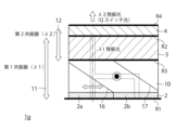
- FIG. 13 is a schematic cross-sectional view of a laser element 1g according to the eighth embodiment.
- the laser device 1g in FIG. 13 has a configuration in which a solid laser medium 3 and a saturable absorber 4 are arranged in this order on the light exit surface side of the polarization splitter 10.
- the laser element 1g in FIG. 13 has a first reflective layer R1 to a fourth reflective layer R4.
- the first reflective layer R1 is arranged on the end surface of the laminated semiconductor layer 2, which is the excitation light source 2, on the opposite side to the light exit surface.
- the second reflective layer R2 is arranged between the solid laser medium 3 and the saturable absorber 4.
- the third reflective layer R3 is arranged between the polarization splitting element 10 and the laser element 1g.
- the fourth reflective layer R4 is arranged on the light exit surface side of the saturable absorber 4.
- the laser element 1g in FIG. 13 has a first resonator 11 and a second resonator 12.
- the first resonator 11 causes light having a first wavelength ⁇ 1 to resonate between the first reflective layer R1 and the second reflective layer R2.
- the second resonator 12 resonates light with a second wavelength ⁇ 2 between the third reflective layer R3 and the fourth reflective layer R4.
- the solid-state laser medium 3 is commonly used as a first resonator 11 and a second resonator 12.
- the pump light that is multiplexed by the polarization splitter 10 and has improved optical output has a small pulse width, high laser peak power, and no jitter. Can emit Q-switched pulsed laser light.
- FIG. 14 is a schematic cross-sectional view showing each layer of the laser element 1g of FIG. 13 in more detail.
- the laminated semiconductor layer 2, which is the excitation light source 2 has two laminated semiconductor regions. Hereinafter, these two stacked semiconductor regions will be referred to as a first stacked semiconductor region 2a and a second stacked semiconductor region 2b.
- the TM polarized light performs resonance operation between the first laminated semiconductor region 2a, the polarization separation element 10, and the solid-state laser medium 3. Further, the TE polarized light emitted from the second laminated semiconductor region 2b and separated by the polarization splitting element 10 is combined into the TM polarized light inside the polarization splitting element 10.
- the excitation light source 2 consists of a laminated semiconductor layer 2 divided into a first laminated semiconductor region 2a and a second laminated semiconductor region 2b. , a cladding layer 8, a pre-oxidation layer 31, and a first reflective layer R1 are laminated in this order.
- the laser element 1g in FIG. 1 shows a bottom emission type configuration in which continuous wave (CW) excitation light is emitted from the substrate 5, but the CW excitation light is emitted from the first reflective layer R1 side.
- a top-emission type configuration is also possible.
- the substrate 5 is, for example, an n-GaAs substrate 5. Since the n-GaAs substrate 5 absorbs light of the first wavelength ⁇ 1, which is the excitation wavelength of the excitation light source 2, at a constant rate, it is desirable to make it as thin as possible. On the other hand, it is desirable to have a thickness sufficient to maintain mechanical strength during the bonding process described below.
- the active layer 7 emits surface light at a first wavelength ⁇ 1.
- the cladding layers 6 and 8 are, for example, AlGaAs cladding layers.
- the first reflective layer R1 reflects light having a first wavelength ⁇ 1.
- the fifth reflective layer R5 has a constant transmittance for light having the first wavelength ⁇ 1.
- a semiconductor distributed reflective layer DBR: Distributed Bragg Reflector
- a current is injected from the outside through the first reflective layer R1 and the fifth reflective layer R5, recombination and light emission occur in the quantum well in the active layer 7, and laser oscillation at the first wavelength ⁇ 1 is performed.
- a part of the pre-oxidation layer (for example, AlAs layer) 31 on the cladding layer side of the first reflective layer R1 is oxidized to become a post-oxidation layer (for example, Al 2 O 3 layer) 32 .
- the fifth reflective layer R5 is arranged on the n-GaAs substrate 5, for example.
- the fifth reflective layer R5 includes a multilayer reflective film 17 made of Al z1 Ga 1-z1 As/Al z2 Ga 1-z2 As (0 ⁇ z1 ⁇ z2 ⁇ 1) doped with an n-type dopant (for example, silicon).
- the fifth reflective layer R5 is also called n-DBR.
- an n-contact layer 33 is arranged between the fifth reflective layer R5 and the n-GaAs substrate 5.
- the active layer 7 has, for example, a multiple quantum well layer in which an Al x1 In y1 Ga 1-x1-y1 As layer and an Al x3 In y3 Ga 1-x3-y3 As layer are laminated.
- the first reflective layer R1 has, for example, a multiple reflective film made of Alz3Ga1-z3As/AlZ4Ga1-z4As (0 ⁇ z3 ⁇ z4 ⁇ 1) doped with a p-type dopant (for example, carbon).
- the first reflective layer R1 is also called p-DBR.
- Each of the semiconductor layers R5, 6, 7, 8, and R1 in the excitation light source 2 can be formed using a crystal growth method such as MOCVD (metal organic chemical vapor deposition) or MBE (molecular beam epitaxy). After crystal growth, processes such as mesa etching for element isolation, formation of an insulating film, and vapor deposition of an electrode film are performed to enable driving by current injection.
- MOCVD metal organic chemical vapor deposition
- MBE molecular beam epitaxy
- a solid-state laser medium 3 is bonded to the end surface of the n-GaAs substrate 5 of the excitation light source 2 on the side opposite to the fifth reflective layer R5.
- the end surface of the solid-state laser medium 3 on the excitation light source 2 side will be referred to as a first surface F1
- the end surface of the solid-state laser medium 3 on the saturable absorber 4 side will be referred to as a second surface F2.
- the laser pulse output surface of the saturable absorber 4 is referred to as a third surface F3
- the end surface of the excitation light source 2 on the solid-state laser medium 3 side is referred to as a fourth surface F4.
- the end surface of the saturable absorber 4 on the solid-state laser medium 3 side is referred to as a fifth surface F5.
- the fourth surface F4 of the excitation light source 2 is joined to the first surface F1 of the solid-state laser medium 3, and the second surface F2 of the solid-state laser medium 3 is connected to the saturable absorber 4. It is joined to the fifth surface F5 of.
- the laser element 1 in FIG. 1 includes a first resonator 11 and a second resonator 12.
- the first resonator 11 causes light of a first wavelength ⁇ 1 to resonate between the first reflective layer R1 in the excitation light source 2 and the second reflective layer R2 in the solid-state laser medium 3.
- the second resonator 12 resonates light with a second wavelength ⁇ 2 between the third reflective layer R3 in the solid-state laser medium 3 and the fourth reflective layer R4 in the saturable absorber 4.
- the second resonator 12 is also called a Q-switch solid-state laser resonator 12.
- a second reflective layer R2 which is a highly reflective layer, is provided within the solid-state laser medium 3 so that the first resonator 11 can perform stable resonant operation.
- a partial reflection mirror for emitting light of the first wavelength ⁇ 1 to the outside is arranged at the position of the second reflection layer R2 in FIG.
- the second reflective layer R2 is used to confine the power of the excitation light with the first wavelength ⁇ 1 within the first resonator 11, so the second reflective layer R2 is It has a reflective layer.
- first reflective layer R1 the first reflective layer consisting of the excitation light source 2 and the solid-state laser medium 3. It will be done. Therefore, the first resonator 11 has a coupled cavity structure.
- the solid-state laser medium 3 is excited.
- Q-switched laser pulse oscillation occurs in the second resonator 12.
- the second resonator 12 resonates light with a second wavelength ⁇ 2 between the third reflective layer R3 in the solid-state laser medium 3 and the fourth reflective layer R4 in the saturable absorber 4.
- the third reflective layer R3 is a highly reflective layer
- the fourth reflective layer R4 is a partially reflective layer.
- the fourth reflective layer R4 is provided on the end face of the saturable absorber 4, but the fourth reflective layer R4 may be placed on the rear side of the optical axis than the saturable absorber 4.
- the rear of the optical axis is the direction in which light on the optical axis is emitted. That is, the fourth reflective layer R4 does not necessarily need to be provided inside or on the surface of the saturable absorber 4.
- the fourth reflective layer R4 is an output coupling mirror in the second resonator 12.
- excitation light source 2 solid-state laser medium 3, and saturable absorber 4 are shown separately in FIG. 1, they have a laminated structure that is joined and integrated using a joining process.
- bonding processes include surface activated bonding, atomic diffusion bonding, plasma activated bonding, and the like. Alternatively, other bonding (adhesion) processes can be used.
- the electrodes E1 and E2 for injecting current into the first reflective layer R1 and the fifth reflective layer R5 are arranged so that they are not exposed to at least the surface of the n-GaAs substrate 5. .
- electrodes E1 and E2 are arranged on the end surface of the excitation light source 2 on the first reflective layer R1 side.
- the electrode E1 is a p-electrode and is electrically connected to the first reflective layer R1.
- the electrode E2 is an n-electrode and is formed by filling the inner wall of a trench extending from the first reflective layer R1 to the n-contact layer 33 with a conductive material 35 via an insulating film 34.
- this end face can be soldered onto a support substrate (not shown). Even when a plurality of laser elements 1 are arranged in an array, by arranging the electrodes E1 and E2 on the same end face, this end face can be mounted on a support substrate. Note that the shapes and locations of the electrodes E1 and E2 shown in FIG. 1 are merely examples.
- the laser element 1 in FIG. 1 into a laminated structure, it is possible to fabricate a laminated structure and then separate it into pieces by dicing to form a plurality of chips, or to form a plurality of laser elements 1 on one substrate. It becomes easy to form a laser array in which these are arranged in an array.
- the arithmetic mean roughness Ra of each surface layer needs to be about 1 nm or less, preferably 0.5 nm or less.
- Chemical mechanical polishing (CMP) is used to achieve a surface layer with these arithmetic mean roughnesses.
- CMP Chemical mechanical polishing
- a dielectric multilayer film may be disposed between each layer, and each layer may be bonded via the dielectric multilayer film.
- the refractive index n of the GaAs substrate 5, which is the base substrate of the excitation light source 2 at a wavelength of 940 nm is 3.5, which has a higher refractive index than YAG (n: 1.8) or general dielectric multilayer film materials. has. Therefore, when joining the solid-state laser medium 3 and the saturable absorber 4 to the excitation light source 2, it is necessary to prevent optical loss due to refractive index mismatch.
- an antireflection film AR coating film or nonreflection coating film
- an antireflection film that does not reflect the light of the first wavelength ⁇ 1 of the first resonator 11 is disposed between the excitation light source 2 and the solid-state laser medium 3. is desirable.
- an antireflection film an AR coating film or a nonreflection coating film
- Polishing may be difficult depending on the bonding material.
- a material such as SiO 2 that is transparent to the first wavelength ⁇ 1 and the second wavelength ⁇ 2 is formed as a base layer for bonding, and this SiO 2 layer is It may be polished to an average roughness Ra of about 1 nm (preferably 0.5 nm or less) and used as an interface for bonding.
- the underlayer materials other than SiO 2 can be used, and the material is not limited here. Note that a non-reflective film may be provided between SiO 2 which is the material of the underlayer and the base layer.
- the dielectric multilayer film includes a short wave pass filter (SWPF), a long wave pass filter (LWPF), a band pass filter (BPF), and anti-reflection protection.
- SWPF short wave pass filter
- LWPF long wave pass filter
- BPF band pass filter
- AR anti-reflection films
- PVD physical vapor deposition
- a film forming method such as vacuum evaporation, ion-assisted evaporation, sputtering, etc. can be used. It does not matter which film formation method is applied.
- the characteristics of the dielectric multilayer film can be arbitrarily selected.
- the third reflective layer R3 may be a short wavelength transmission filter film
- the second reflective layer R2 may be a long wavelength transmission filter film.
- short wavelength transmission means that light with a first wavelength ⁇ 1 is transmitted and light with a second wavelength ⁇ 2 is reflected.
- long wavelength transmission means that light with a first wavelength ⁇ 1 is reflected and light with a second wavelength ⁇ 2 is transmitted.
- a diffraction grating may be provided inside the second resonator 12 to convert the polarization state of the emitted laser pulse from random polarization to linear polarization.
- a diffraction grating may be provided inside the second resonator 12 to convert the polarization state of the emitted laser pulse from random polarization to linear polarization.
- a film of a material such as SiO 2 on the fine groove portion of the photonic crystal structure or the diffraction grating and polishing it, it can be used as an interface for bonding.
- the solid-state laser medium 3 is excited.
- the saturable absorber 4 is bonded to the solid-state laser medium 3, at the initial stage when laser oscillation with the first wavelength ⁇ 1 occurs, spontaneously emitted light from the solid-state laser medium 3 is absorbed by the saturable absorber 4. Since the light is absorbed, optical feedback by the fourth reflective layer R4 on the emission surface side of the saturable absorber 4 does not occur, and Q-switched laser oscillation does not occur.
- the TE polarized light is combined with the TM polarized light inside the polarized light splitting element 10 and outputted, so that the light emitted from the polarized light splitting element 10 is Output can be increased.
- the first resonator 11 includes a first reflective layer R1 disposed on the end surface of the first laminated semiconductor region 2a and the second laminated semiconductor region 2b opposite to the light exit surface, a solid laser medium 3, and a saturable absorber. The light having the first wavelength ⁇ 1 is caused to resonate with the second reflective layer R2 between the two reflective layers R2.
- the second resonator 12 has a third reflective layer R3 between the polarization splitting element 10 and the solid-state laser medium 3, and a fourth reflective layer R4 on the light exit surface side of the saturable absorber 4. Resonates light with two wavelengths ⁇ 2.
- FIG. 15 is a plan view and a cross-sectional view showing a plurality of laser elements 1h arranged in an array.
- the laminated semiconductor layer 2 constituting the excitation light source 2 is divided into a plurality of laminated semiconductor regions 2a and 2b.
- One of the two adjacent laminated semiconductor regions 2a and 2b is used to output TM polarized light, and the other is used to combine TE polarized light into TM polarized light. Therefore, while excitation light is emitted from one MesaA of the two light emitting parts corresponding to the two adjacent stacked semiconductor regions 2a and 2b, almost no excitation light is emitted from the other MesaB. Therefore, the light emitting section from which the excitation light is emitted may be made larger.
- a plurality of laser elements 1h with increased optical output by providing the polarization separation element 10 are arranged in two dimensions, so that the laser element 1h is capable of high optical output and has a long life. can be realized.
- FIG. 16A is a cross-sectional view of the laser amplification element 50 according to the present disclosure
- FIG. 16B is a perspective view of the laser amplification element 50 according to the present disclosure
- FIG. 16C is a plan view schematically showing the optical path of the laser beam within the laser amplification element 50.
- the laser amplifying element 50 includes an excitation light source 53 disposed on a support substrate 51 via a submount substrate 52, a polarization separation element 60 disposed on the excitation light source 53, and a polarization separation element 53. 60, and the saturable absorber 4 is not provided.
- the solid-state laser medium 54 is, for example, Yb:YAG.
- a first resonator 55 is configured by the excitation light source 53 and the solid-state laser medium 54, and light with a first wavelength ⁇ 1 is resonated in the vertical direction (stacking direction) in FIG. 16A.
- the first resonator 55 has the first wavelength ⁇ 1 between the first reflective layer R1 (p-DBR72) in the excitation light source 53 and the second reflective layer R2 in the solid-state laser medium 54. Make light resonate.
- the solid-state laser medium 3 in the laser element 1 in FIG. 1 has a third reflective layer R3 on the end face facing the excitation light source 2, and a fourth reflective layer R4 on the end face facing the saturable absorber 4.
- the solid-state laser medium 54 in FIG. 16A does not require a reflective layer on the end face facing the excitation light source 53, and has a second reflective layer R2 on the opposite end face.
- the laser amplification element 50 includes a first reflecting member 56 and a second reflecting member 57 disposed along the opposing first side surface 54S1 and second side surface 54S2 of the solid-state laser medium 54,
- the solid-state laser medium 54 functions as an amplification medium 83 that causes light of the second wavelength ⁇ 2 to reciprocate a plurality of times between the first reflecting member 56 and the second reflecting member 57.
- the first reflecting member 56 and the second reflecting member 57 may have flat reflecting mirrors, or may have convex reflecting mirrors in order to increase the optical density during the amplification process and avoid optical damage to the material. It may have.
- the first reflecting member 56 and the second reflecting member 57 are arranged at a distance from the first side surface 54S1 and the second side surface 54S2 of the solid-state laser medium 54, but the first side surface 54S1 and the second side surface 54S2 Alternatively, a multilayer film may be formed by laminating at least one of a semiconductor material, a metal material, and a dielectric material, and these multilayer films may be used as a reflecting mirror.
- the laser amplification element 50 includes an optical input section IN provided along the first side surface 54S1 and an optical output section OUT provided along the second side surface 54S2.
- the light input unit IN inputs weak light (seed light) having a second wavelength ⁇ 2 into the first side surface 54S1.
- the light having the second wavelength ⁇ 2 travels back and forth in the amplification medium 83 multiple times and is emitted from the light output section OUT.
- the laser amplification element 50 has a polarization splitting element 60 similar to the polarization splitting element 10 according to the first to ninth embodiments.
- the polarization separation element 60 By providing the polarization separation element 60, the light output emitted from the polarization separation element 10 can be increased.
- the laser amplification element 50 shown in FIGS. 16A to 16C may include a cooling member 62.
- the cooling member 62 is joined to the side surfaces of the excitation light source 53, the polarization separation element 60, and the solid-state laser medium 54, and radiates heat generated by at least one of the excitation light source 53, the polarization separation element 60, and the solid-state laser medium 54. do.
- the cooling member 62 is, for example, a metal material with high thermal conductivity such as Cu.
- the cooling member 62 may be joined to a package (not shown), and heat may be radiated from the cooling member 62 to the package.
- the support substrate 51 in the laser amplification element 50 shown in FIGS. 16A to 16C is, for example, a Cu substrate, and a submount substrate 52 is disposed thereon.
- the submount substrate 52 has, for example, a laminated structure of a SiC layer 64 and an AuSn layer 65, and a p-electrode 73 and an n-electrode 74 of the excitation light source 53 are bonded to and electrically insulated from each other on the AuSn layer 65. .
- the excitation light source 53 is a laminated semiconductor layer 2 in which an n-contact layer 67, an n-DBR 68, a cladding layer 69, an active layer 70, a cladding layer 71, and a p-DBR 72 are laminated in order on an n-GaAs substrate 66. .
- p electrodes 73 and n electrodes 74 are arranged alternately.
- the p-electrode 73 is electrically connected to the p-DBR 72
- the n-electrode 74 is electrically electrically connected to the n-DBR 68 via a via 75.
- a laser amplification element 50 includes a first resonator 55, similar to FIG. 1.
- the first resonator 55 resonates light with a first wavelength ⁇ 1 between the first reflective layer R1 in the excitation light source 53 and the second reflective layer R2 in the solid laser medium 54.
- the first reflective layer R1 is a p-DBR 72
- the second reflective layer R2 is arranged, for example, on the upper surface of the heat exhaust member 61.
- the heat exhaust member 61 may be omitted.
- the solid laser medium 54 is excited by the resonance operation of the light having the first wavelength ⁇ 1 by the first resonator 55.
- FIG. 16A the resonance operation by the first resonator 55 is schematically shown with thin lines.
- the amplified light (seed light) having the second wavelength ⁇ 2 is made to enter the solid-state laser medium 54 in the excited state from the right end to the left in FIG. 16A. This causes stimulated emission of the light to be amplified, and the light to be amplified is laser amplified.
- Yb:YAG when used as the amplification medium 83, if a laser beam with a wavelength of 1030 nm is used as the seed light, it will be absorbed in an unexcited region of the amplification medium 83, and sufficient amplification cannot be achieved. happens. Therefore, when Yb:YAG is used as the amplification medium 83, it is possible to use seed light with a wavelength of 1050 nm that does not cause optical absorption even in an unexcited state. In this case, the wavelength of the seed light is not limited to 1050 nm since it is sufficient that light absorption does not occur even in an unexcited state.
- the optical configuration can be greatly simplified and miniaturization becomes possible.
- the size of the solid-state laser medium 54 in the laser amplification element 50 according to the present disclosure is not limited by the absorption length of the excitation light, the area of the solid-state laser medium 54 can be increased regardless of the absorption length of the excitation light. By increasing the area of the solid-state laser medium 54, the amplification factor of the laser amplification element 50 can be further improved.
- the laser amplification element 50 can integrally bond the excitation light source 53 made of the laminated semiconductor layer 2 and the solid-state laser medium 54, and can be manufactured using a general-purpose semiconductor process, so that miniaturization is possible. It is easy and can reduce manufacturing costs.
- a medical imaging system is a medical system using imaging technology, such as an endoscope system or a microscope system.
- FIG. 17 is a diagram illustrating an example of a schematic configuration of an endoscope system 5000 to which the technology according to the present disclosure can be applied.
- FIG. 18 is a diagram showing an example of the configuration of an endoscope 5001 and a CCU (Camera Control Unit) 5039.
- an operator for example, a doctor
- FIG. 17 an operator 5067 who is a participant in the surgery is shown performing surgery on a patient 5071 on a patient bed 5069 using the endoscope system 5000.
- FIG. 17 is a diagram illustrating an example of a schematic configuration of an endoscope system 5000 to which the technology according to the present disclosure can be applied.
- FIG. 18 is a diagram showing an example of the configuration of an endoscope 5001 and a CCU (Camera Control Unit) 5039.
- an operator for example, a doctor
- FIG. 17 an operator 5067 who is a participant in the surgery is shown performing surgery on a patient 5071 on a patient bed 5069 using the endoscope
- an endoscope system 5000 supports an endoscope 5001 that is a medical imaging device, a CCU 5039, a light source device 5043, a recording device 5053, an output device 5055, and an endoscope 5001.
- an insertion aid called a trocar 5025 is inserted into the patient 5071. Then, the scope 5003 connected to the endoscope 5001 and the surgical instrument 5021 are inserted into the body of the patient 5071 via the trocar 5025.
- the surgical tool 5021 is, for example, an energy device such as an electric scalpel, forceps, or the like.
- a surgical image which is a medical image showing the inside of the patient's 5071, captured by the endoscope 5001 is displayed on the display device 5041.
- the surgeon 5067 uses the surgical tool 5021 to treat the surgical target while viewing the surgical image displayed on the display device 5041.
- the medical image is not limited to a surgical image, but may be a diagnostic image captured during diagnosis.
- the endoscope 5001 is an imaging unit that images the inside of the body of a patient 5071, and for example, as shown in FIG.
- a camera 5005 includes a zoom optical system 50052 that enables optical zoom, a focus optical system 50053 that enables focus adjustment by changing the focal length of an imaging unit, and a light receiving element 50054.
- the endoscope 5001 generates a pixel signal by focusing light onto a light receiving element 50054 via the connected scope 5003, and outputs the pixel signal to the CCU 5039 through a transmission system.
- the scope 5003 is an insertion section that has an objective lens at its tip and guides light from the connected light source device 5043 into the body of the patient 5071.
- the scope 5003 is, for example, a rigid scope if it is a rigid scope, or a flexible scope if it is a flexible scope.
- the scope 5003 may be a direct scope or an oblique scope.
- the pixel signal may be a signal based on a signal output from a pixel, such as a RAW signal or an image signal.
- a configuration may be adopted in which a memory is installed in the transmission system that connects the endoscope 5001 and the CCU 5039, and parameters related to the endoscope 5001 and the CCU 5039 are stored in the memory.
- the memory may be placed, for example, on a connection part of a transmission system or on a cable.
- the parameters of the endoscope 5001 at the time of shipment and the parameters that changed when the power was applied may be stored in a transmission system memory, and the operation of the endoscope may be changed based on the parameters read from the memory. Further, an endoscope and a transmission system may be combined together and called an endoscope.
- the light receiving element 50054 is a sensor that converts received light into a pixel signal, and is, for example, a CMOS (Complementary Metal Oxide Semiconductor) type image sensor.
- the light receiving element 50054 is preferably an image sensor having a Bayer array and capable of color photography.
- the light receiving element 50054 can be used, for example, in 4K (horizontal pixels 3840 x vertical pixels 2160), 8K (horizontal pixels 7680 x vertical pixels 4320), or square 4K (horizontal pixels 3840 or more x vertical pixels 3840 or more). It is preferable that the image sensor has the number of pixels corresponding to the resolution.
- the light receiving element 50054 may be a single sensor chip or may be a plurality of sensor chips. For example, a configuration may be adopted in which a prism that separates incident light into predetermined wavelength bands is provided, and each wavelength band is imaged by a different light receiving element. Further, a plurality of light receiving elements may be provided for stereoscopic viewing.
- the light receiving element 50054 may be a sensor including an arithmetic processing circuit for image processing in a chip structure, or may be a ToF (Time of Flight) sensor.
- the transmission system is, for example, an optical fiber cable or wireless transmission. Wireless transmission may be performed as long as pixel signals generated by the endoscope 5001 can be transmitted; for example, the endoscope 5001 and the CCU 5039 may be wirelessly connected, or the endoscope 5001 and the CCU 5039 may be wirelessly connected, or the endoscope 5001 and the CCU 5039 may be wirelessly connected, or the endoscope Mirror 5001 and CCU 5039 may be connected.
- the endoscope 5001 may simultaneously transmit not only the pixel signal but also information related to the pixel signal (for example, pixel signal processing priority, synchronization signal, etc.).
- the endoscope may have a scope and a camera integrated, or may have a configuration in which a light receiving element is provided at the distal end of the scope.
- the CCU 5039 is a control device that centrally controls the connected endoscope 5001 and light source device 5043, and for example, as shown in FIG. It is a processing device. Further, the CCU 5039 may centrally control the connected display device 5041, recording device 5053, and output device 5055. For example, the CCU 5039 controls the irradiation timing and irradiation intensity of the light source device 5043, and the type of irradiation light source. The CCU 5039 also performs image processing such as development processing (for example, demosaic processing) and correction processing on the pixel signals output from the endoscope 5001, and displays the processed pixel signals (for example, image ) is output.
- image processing such as development processing (for example, demosaic processing) and correction processing on the pixel signals output from the endoscope 5001, and displays the processed pixel signals (for example, image ) is output.
- the CCU 5039 transmits a control signal to the endoscope 5001 to control the drive of the endoscope 5001.
- the control signal is, for example, information regarding imaging conditions such as the magnification and focal length of the imaging section.
- the CCU 5039 may have an image down-conversion function and may be configured to be able to simultaneously output a high resolution (for example, 4K) image to the display device 5041 and a low resolution (for example, HD) image to the recording device 5053.
- the CCU5039 is connected to external devices (for example, a recording device, a display device, an output device, a support device) via an IP converter that converts signals into a predetermined communication protocol (for example, IP (Internet Protocol)).
- IP Internet Protocol
- the connection between the IP converter and the external device may be configured by a wired network, or a part or all of the network may be configured by a wireless network.
- the IP converter on the CCU5039 side has a wireless communication function, and the received video is sent to an IP switcher or output via a wireless communication network such as a 5th generation mobile communication system (5G) or a 6th generation mobile communication system (6G). It may also be sent to the side IP converter.
- 5G 5th generation mobile communication system
- 6G 6th generation mobile communication system
- the light source device 5043 is a device capable of emitting light in a predetermined wavelength band, and includes, for example, a plurality of light sources and a light source optical system that guides light from the plurality of light sources.
- the light source is, for example, a xenon lamp, an LED light source, or an LD light source.
- the light source device 5043 has, for example, LED light sources corresponding to each of the three primary colors R, G, and B, and emits white light by controlling the output intensity and output timing of each light source.
- the light source device 5043 may include a light source capable of emitting special light used for special light observation, in addition to a light source that emit normal light used for normal light observation.
- Special light is light in a predetermined wavelength band that is different from normal light that is used for normal light observation, and includes, for example, near-infrared light (light with a wavelength of 760 nm or more), infrared light, blue light, and ultraviolet light. It is.
- the normal light is, for example, white light or green light.
- narrowband light observation which is a type of special light observation, blue light and green light are irradiated alternately to take advantage of the wavelength dependence of light absorption in body tissues to target specific tissues such as blood vessels on the surface of mucous membranes. can be photographed with high contrast.
- fluorescence observation which is a type of special light observation
- excitation light that excites the drug injected into body tissue is irradiated, and the fluorescence emitted by the body tissue or the labeled drug is received to obtain a fluorescence image.
- body tissues etc. that are difficult for the surgeon to see under normal light.
- a drug such as indocyanine green (ICG) injected into body tissue is irradiated with infrared light having an excitation wavelength band, and by receiving the fluorescence of the drug, the body tissue is This makes it easier to see the structure and affected area.
- ICG indocyanine green
- a drug for example, 5-ALA
- the type of irradiation light of the light source device 5043 is set under the control of the CCU 5039.
- the CCU 5039 may have a mode in which normal light observation and special light observation are performed alternately by controlling the light source device 5043 and the endoscope 5001. At this time, it is preferable that information based on the pixel signal obtained by special light observation be superimposed on the pixel signal obtained by normal light observation.
- the special light observation may be infrared light observation to see deeper than the organ surface by irradiating infrared light, or multispectral observation using hyperspectral spectroscopy.
- photodynamic therapy may be combined.
- the recording device 5053 is a device that records pixel signals (for example, images) acquired from the CCU 5039, and is, for example, a recorder.
- the recording device 5053 records the image acquired from the CCU 5039 on an HDD, SDD, or optical disc.
- the recording device 5053 may be connected to a network within the hospital and may be accessible from equipment outside the operating room. Further, the recording device 5053 may have an image down-conversion function or an image up-conversion function.
- the display device 5041 is a device capable of displaying images, and is, for example, a display monitor.
- the display device 5041 displays a display image based on the pixel signal acquired from the CCU 5039.
- the display device 5041 may also function as an input device that enables line-of-sight recognition, voice recognition, and instruction input using gestures by being equipped with a camera and a microphone.
- the output device 5055 is a device that outputs the information acquired from the CCU 5039, and is, for example, a printer.
- the output device 5055 prints a print image based on the pixel signal acquired from the CCU 5039 on paper, for example.
- the support device 5027 is a multi-jointed arm that includes a base portion 5029 having an arm control device 5045, an arm portion 5031 extending from the base portion 5029, and a holding portion 5032 attached to the tip of the arm portion 5031.
- the arm control device 5045 is configured by a processor such as a CPU, and controls the drive of the arm portion 5031 by operating according to a predetermined program.
- the support device 5027 controls parameters such as the length of each link 5035 constituting the arm portion 5031 and the rotation angle and torque of each joint 5033 using an arm control device 5045, so that, for example, the endoscope 5001 held by the holding portion 5032 control the position and posture of Thereby, the endoscope 5001 can be changed to a desired position or posture, the scope 5003 can be inserted into the patient 5071, and the observation area inside the body can be changed.
- the support device 5027 functions as an endoscope support arm that supports the endoscope 5001 during surgery. Thereby, the support device 5027 can take the place of a scopist who is an assistant holding the endoscope 5001.
- the support device 5027 may be a device that supports a microscope device 5301, which will be described later, and can also be referred to as a medical support arm.
- the support device 5027 may be controlled by an autonomous control method by the arm control device 5045, or by a control method controlled by the arm control device 5045 based on user input.
- the control method is a master-slave method in which the support device 5027 as a slave device (replica device), which is a patient cart, is controlled based on the movement of a master device (primary device), which is an operator console at the user's hand. But that's fine.
- the support device 5027 may be remotely controlled from outside the operating room.
- an example of the endoscope system 5000 to which the technology according to the present disclosure can be applied has been described above.
- the technology according to the present disclosure may be applied to a microscope system.
- FIG. 19 is a diagram illustrating an example of a schematic configuration of a microsurgical system to which the technology according to the present disclosure can be applied.
- the same components as those of the endoscope system 5000 are denoted by the same reference numerals, and redundant description thereof will be omitted.
- FIG. 19 schematically shows a surgeon 5067 performing surgery on a patient 5071 on a patient bed 5069 using a microsurgery system 5300.
- a microscope device 5301 that replaces the endoscope 5001 is illustrated in a simplified manner.
- the microscope device 5301 in this description may refer to the microscope section 5303 provided at the tip of the link 5035, or may refer to the entire configuration including the microscope section 5303 and the support device 5027.
- an image of the surgical site taken by a microscope device 5301 using a microsurgery system 5300 is enlarged and displayed on a display device 5041 installed in the operating room.
- the display device 5041 is installed at a position facing the surgeon 5067, and the surgeon 5067 can perform operations such as resection of the affected area while observing the state of the surgical site using the image displayed on the display device 5041.
- Various measures are taken against.
- Microsurgical systems are used, for example, in ophthalmic surgery and brain surgery.
- the support device 5027 may support another observation device or another surgical tool instead of the endoscope 5001 or the microscope section 5303 at its tip.
- the other observation device for example, forceps, a forceps, a pneumoperitoneum tube for pneumoperitoneum, or an energy treatment tool for incising tissue or sealing blood vessels by cauterization may be applied.
- the technology according to the present disclosure can be suitably applied to the surgical instrument 5021 among the configurations described above. Specifically, by irradiating the affected area of the patient with short laser pulses from the laser element 1 according to the present embodiment, the affected area can be treated more safely and reliably without damaging the surrounding area. can.
- the present technology can have the following configuration.
- a laminated semiconductor layer having a first reflective layer for light of a first wavelength and an active layer that performs surface emission of the first wavelength; a second reflective layer for light of the first wavelength, which is disposed closer to the light exit surface than the laminated semiconductor layer; a polarization splitting element that individually resonates and combines orthogonally polarized lights included in the light emitted from the laminated semiconductor layer between the first reflective layer and the second reflective layer; laser element.
- the laminated semiconductor layer has a plurality of laminated semiconductor regions corresponding to the orthogonal polarized light, and the polarization separation element transmits the corresponding polarized light to the plurality of laminated semiconductor regions for each of the plurality of laminated semiconductor regions.
- the laser element according to (1) wherein the first reflective layer and the second reflective layer individually resonate and combine.
- the polarization splitting element is arranged between a first surface that is in contact with the light exit surface of the laminated semiconductor layer, and the first reflective layer and the second reflective layer on the opposite side of the first surface.
- the orthogonal polarized lights include orthogonal polarized lights of different wavelengths, and the polarization separation element separates each of the orthogonal polarized lights including orthogonal polarized lights of different wavelengths to the first reflective layer.
- the orthogonal polarized light includes TM (Transverse Magnetic) polarized light and TE (Transverse Electric) polarized light
- the polarization separation element has a laminate in which a plurality of polarization separation films and a plurality of reflection films are alternately stacked at intervals, and The laminate has a cut surface cut in a direction of 45 degrees with respect to the normal direction of the laminate surface,
- the laser device according to any one of (1) to (6), wherein the polarization separation element is arranged such that the normal direction of the cut plane is parallel to the normal direction of the laminated semiconductor layer.
- the polarization separation element includes a birefringent material that separates the light emitted from the laminated semiconductor layer into the orthogonal polarized light. .
- laser element. (10) a third reflective layer disposed on the first end face of the laser medium on the polarization splitting element side for light of the second wavelength;
- a third reflective layer for light of the second wavelength which is disposed on the end face of the laser medium on the side facing the polarization splitting element;
- the third reflective layer is disposed closer to the light exit surface than the second reflective layer.
- the second reflective layer is disposed between the third reflective layer and the fourth reflective layer.
- Each of the laminated semiconductor layer, the polarization splitting element, the laser medium, and the saturable absorber includes a plurality of light emitting portions arranged at predetermined intervals and emitting pulsed laser light of the second wavelength.
- the laser element according to any one of (15) to (18), which is divided into a plurality of regions in correspondence with each other.
- a laser element (20) a laser element;
- An electronic device comprising: a control unit that controls emitting light from the laser element;
- the laser element is a laminated semiconductor layer having a first reflective layer for light of a first wavelength and an active layer that performs surface emission of the first wavelength; a second reflective layer for light of the first wavelength, which is disposed closer to the light exit surface than the laminated semiconductor layer; a polarization splitting element that individually resonates and combines each of the plurality of polarized lights included in the light emitted from the laminated semiconductor layer between the first reflective layer and the second reflective layer; Electronics.
- Al2O3 layer 33 contact layer, 34 insulating film, 35 conductive material, 50 laser amplification element, 51 support substrate, 52 submount substrate, 53 excitation light source, 54 solid laser medium, 55 first resonator, 56 first reflecting member, 57 second reflecting member, 60 polarization separation element, 61 heat exhaust member, 62 cooling member, 64 SiC layer, 65 AuSn layer, 66 n-GaAs substrate , 67 contact layer, 69 cladding layer, 70 active layer, 71 cladding layer, 73 p electrode, 74 n electrode, 75 via, 83 amplification medium, 100 laser element
Landscapes
- Physics & Mathematics (AREA)
- Electromagnetism (AREA)
- Optics & Photonics (AREA)
- Engineering & Computer Science (AREA)
- Plasma & Fusion (AREA)
- Condensed Matter Physics & Semiconductors (AREA)
- General Physics & Mathematics (AREA)
- Life Sciences & Earth Sciences (AREA)
- Sustainable Development (AREA)
- Chemical & Material Sciences (AREA)
- Crystallography & Structural Chemistry (AREA)
- Lasers (AREA)
Priority Applications (4)
| Application Number | Priority Date | Filing Date | Title |
|---|---|---|---|
| JP2024510920A JP7737638B2 (ja) | 2022-03-30 | 2022-03-30 | レーザ素子及び電子機器 |
| PCT/JP2022/016104 WO2023188146A1 (ja) | 2022-03-30 | 2022-03-30 | レーザ素子及び電子機器 |
| DE112022006961.9T DE112022006961T5 (de) | 2022-03-30 | 2022-03-30 | Laserelement und elektronische vorrichtung |
| US18/849,940 US20250329990A1 (en) | 2022-03-30 | 2022-03-30 | Laser element and electronic device |
Applications Claiming Priority (1)
| Application Number | Priority Date | Filing Date | Title |
|---|---|---|---|
| PCT/JP2022/016104 WO2023188146A1 (ja) | 2022-03-30 | 2022-03-30 | レーザ素子及び電子機器 |
Publications (1)
| Publication Number | Publication Date |
|---|---|
| WO2023188146A1 true WO2023188146A1 (ja) | 2023-10-05 |
Family
ID=88199795
Family Applications (1)
| Application Number | Title | Priority Date | Filing Date |
|---|---|---|---|
| PCT/JP2022/016104 Ceased WO2023188146A1 (ja) | 2022-03-30 | 2022-03-30 | レーザ素子及び電子機器 |
Country Status (4)
| Country | Link |
|---|---|
| US (1) | US20250329990A1 (https=) |
| JP (1) | JP7737638B2 (https=) |
| DE (1) | DE112022006961T5 (https=) |
| WO (1) | WO2023188146A1 (https=) |
Cited By (2)
| Publication number | Priority date | Publication date | Assignee | Title |
|---|---|---|---|---|
| WO2025105353A1 (ja) * | 2023-11-14 | 2025-05-22 | 日本碍子株式会社 | 複合基板および複合基板の製造方法 |
| WO2025197414A1 (ja) * | 2024-03-18 | 2025-09-25 | ソニーグループ株式会社 | レーザ素子、スイッチ素子、及び測距システム |
Citations (4)
| Publication number | Priority date | Publication date | Assignee | Title |
|---|---|---|---|---|
| CN102244358A (zh) * | 2011-06-02 | 2011-11-16 | 天津奇谱光电技术有限公司 | 一种外腔式可调谐激光器 |
| JP2014199923A (ja) * | 2013-03-13 | 2014-10-23 | 株式会社リコー | 面発光レーザアレイ、光源装置、及び面発光レーザアレイの製造方法。 |
| WO2018167975A1 (ja) * | 2017-03-17 | 2018-09-20 | 三菱電機株式会社 | レーザ発振装置 |
| WO2021106757A1 (ja) * | 2019-11-28 | 2021-06-03 | ソニー株式会社 | レーザ素子、レーザ素子の製造方法、レーザ装置およびレーザ増幅素子 |
-
2022
- 2022-03-30 DE DE112022006961.9T patent/DE112022006961T5/de active Pending
- 2022-03-30 WO PCT/JP2022/016104 patent/WO2023188146A1/ja not_active Ceased
- 2022-03-30 US US18/849,940 patent/US20250329990A1/en active Pending
- 2022-03-30 JP JP2024510920A patent/JP7737638B2/ja active Active
Patent Citations (4)
| Publication number | Priority date | Publication date | Assignee | Title |
|---|---|---|---|---|
| CN102244358A (zh) * | 2011-06-02 | 2011-11-16 | 天津奇谱光电技术有限公司 | 一种外腔式可调谐激光器 |
| JP2014199923A (ja) * | 2013-03-13 | 2014-10-23 | 株式会社リコー | 面発光レーザアレイ、光源装置、及び面発光レーザアレイの製造方法。 |
| WO2018167975A1 (ja) * | 2017-03-17 | 2018-09-20 | 三菱電機株式会社 | レーザ発振装置 |
| WO2021106757A1 (ja) * | 2019-11-28 | 2021-06-03 | ソニー株式会社 | レーザ素子、レーザ素子の製造方法、レーザ装置およびレーザ増幅素子 |
Cited By (2)
| Publication number | Priority date | Publication date | Assignee | Title |
|---|---|---|---|---|
| WO2025105353A1 (ja) * | 2023-11-14 | 2025-05-22 | 日本碍子株式会社 | 複合基板および複合基板の製造方法 |
| WO2025197414A1 (ja) * | 2024-03-18 | 2025-09-25 | ソニーグループ株式会社 | レーザ素子、スイッチ素子、及び測距システム |
Also Published As
| Publication number | Publication date |
|---|---|
| JP7737638B2 (ja) | 2025-09-11 |
| DE112022006961T5 (de) | 2025-01-09 |
| US20250329990A1 (en) | 2025-10-23 |
| JPWO2023188146A1 (https=) | 2023-10-05 |
Similar Documents
| Publication | Publication Date | Title |
|---|---|---|
| JP7733881B2 (ja) | レーザ素子及び電子機器 | |
| US20240213733A1 (en) | Laser element and electronic device | |
| JP7737638B2 (ja) | レーザ素子及び電子機器 | |
| US8416832B2 (en) | Switchable dual wavelength solid state laser | |
| WO2024048420A1 (ja) | レーザ素子 | |
| US20100272145A1 (en) | Vecsel-pumped solid-state laser | |
| JP7103082B2 (ja) | 固体レーザ装置 | |
| JP7723913B2 (ja) | レーザ素子及び電子機器 | |
| WO2024150795A1 (ja) | レーザ素子及び電子機器 | |
| JP7754164B2 (ja) | レーザ素子及び電子機器 | |
| CN102484346B (zh) | 单片侧面泵浦的固态激光器及其应用 | |
| CN113314936B (zh) | 一种多波长激光手术刀 | |
| EP3664135A1 (en) | Superluminescent diodes and diode modules | |
| WO2024203427A1 (ja) | レーザ素子及び電子機器 | |
| US20190006813A1 (en) | Diode Pumped High Peak Power Laser System for Multi-Photon Applications | |
| WO2025192044A1 (ja) | レーザ素子及び電子機器 | |
| EP2392056A1 (en) | Wavelength switching by cavity length control in a pr-doped rgb laser | |
| WO2024203811A1 (ja) | 面発光素子 | |
| AU2010262139A1 (en) | A monolithic, side pumped solid-state laser and applications thereof | |
| JP2006147732A (ja) | 医療用レーザ装置 | |
| JP2008147687A (ja) | 眼科用レーザ装置 | |
| WO2022249582A1 (ja) | 光共振器およびレーザ装置 | |
| JP2004279739A (ja) | レーザ装置 | |
| WO2021095523A1 (ja) | 垂直外部共振器型面発光レーザ | |
| JP2016015476A (ja) | 面発光レーザアレイ、固体レーザ装置、およびそれを備えた被検体情報取得装置 |
Legal Events
| Date | Code | Title | Description |
|---|---|---|---|
| 121 | Ep: the epo has been informed by wipo that ep was designated in this application |
Ref document number: 22935291 Country of ref document: EP Kind code of ref document: A1 |
|
| ENP | Entry into the national phase |
Ref document number: 2024510920 Country of ref document: JP Kind code of ref document: A |
|
| WWE | Wipo information: entry into national phase |
Ref document number: 18849940 Country of ref document: US |
|
| WWE | Wipo information: entry into national phase |
Ref document number: 112022006961 Country of ref document: DE |
|
| 122 | Ep: pct application non-entry in european phase |
Ref document number: 22935291 Country of ref document: EP Kind code of ref document: A1 |
|
| WWP | Wipo information: published in national office |
Ref document number: 18849940 Country of ref document: US |