WO2023171333A1 - Dispositif de détection de lumière et instrument électronique - Google Patents
Dispositif de détection de lumière et instrument électronique Download PDFInfo
- Publication number
- WO2023171333A1 WO2023171333A1 PCT/JP2023/005917 JP2023005917W WO2023171333A1 WO 2023171333 A1 WO2023171333 A1 WO 2023171333A1 JP 2023005917 W JP2023005917 W JP 2023005917W WO 2023171333 A1 WO2023171333 A1 WO 2023171333A1
- Authority
- WO
- WIPO (PCT)
- Prior art keywords
- group
- image sensor
- pixel
- neuron
- neural network
- Prior art date
Links
- 238000001514 detection method Methods 0.000 title claims abstract description 11
- 210000002569 neuron Anatomy 0.000 claims abstract description 133
- 238000013528 artificial neural network Methods 0.000 claims abstract description 84
- 230000007175 bidirectional communication Effects 0.000 claims abstract description 10
- 238000010304 firing Methods 0.000 claims description 53
- 238000012545 processing Methods 0.000 claims description 41
- 238000004364 calculation method Methods 0.000 claims description 32
- 230000004069 differentiation Effects 0.000 claims description 16
- 238000000034 method Methods 0.000 claims description 15
- 230000008569 process Effects 0.000 claims description 12
- 238000006243 chemical reaction Methods 0.000 claims description 11
- 230000006854 communication Effects 0.000 claims description 9
- 238000004891 communication Methods 0.000 claims description 9
- 230000002123 temporal effect Effects 0.000 claims description 9
- 230000000737 periodic effect Effects 0.000 claims description 8
- 239000004065 semiconductor Substances 0.000 claims description 7
- 239000000758 substrate Substances 0.000 claims description 6
- 239000012528 membrane Substances 0.000 claims description 5
- 230000004044 response Effects 0.000 claims description 4
- 230000036279 refractory period Effects 0.000 claims description 3
- 238000005516 engineering process Methods 0.000 abstract description 8
- 238000010586 diagram Methods 0.000 description 25
- 230000008859 change Effects 0.000 description 13
- 238000003384 imaging method Methods 0.000 description 10
- 238000012805 post-processing Methods 0.000 description 10
- 238000003062 neural network model Methods 0.000 description 7
- 230000007704 transition Effects 0.000 description 5
- 230000006870 function Effects 0.000 description 4
- 238000007781 pre-processing Methods 0.000 description 4
- 210000000225 synapse Anatomy 0.000 description 4
- 230000001186 cumulative effect Effects 0.000 description 3
- 230000000694 effects Effects 0.000 description 3
- 230000003287 optical effect Effects 0.000 description 3
- 230000009471 action Effects 0.000 description 2
- 230000006872 improvement Effects 0.000 description 2
- 230000003796 beauty Effects 0.000 description 1
- 230000005540 biological transmission Effects 0.000 description 1
- 230000015572 biosynthetic process Effects 0.000 description 1
- 230000004397 blinking Effects 0.000 description 1
- 210000004204 blood vessel Anatomy 0.000 description 1
- 230000000295 complement effect Effects 0.000 description 1
- 238000000605 extraction Methods 0.000 description 1
- 230000005484 gravity Effects 0.000 description 1
- 230000010354 integration Effects 0.000 description 1
- 238000012423 maintenance Methods 0.000 description 1
- 238000005259 measurement Methods 0.000 description 1
- 230000007246 mechanism Effects 0.000 description 1
- 229910044991 metal oxide Inorganic materials 0.000 description 1
- 150000004706 metal oxides Chemical class 0.000 description 1
- 239000000203 mixture Substances 0.000 description 1
- 238000005457 optimization Methods 0.000 description 1
- 230000001151 other effect Effects 0.000 description 1
- 230000002093 peripheral effect Effects 0.000 description 1
- 230000002265 prevention Effects 0.000 description 1
- 230000008707 rearrangement Effects 0.000 description 1
- 230000009467 reduction Effects 0.000 description 1
- 210000004761 scalp Anatomy 0.000 description 1
- 230000035945 sensitivity Effects 0.000 description 1
- 230000008054 signal transmission Effects 0.000 description 1
- 239000007787 solid Substances 0.000 description 1
- 230000001360 synchronised effect Effects 0.000 description 1
- 239000002699 waste material Substances 0.000 description 1
Images


Classifications
-
- G—PHYSICS
- G06—COMPUTING; CALCULATING OR COUNTING
- G06N—COMPUTING ARRANGEMENTS BASED ON SPECIFIC COMPUTATIONAL MODELS
- G06N3/00—Computing arrangements based on biological models
- G06N3/02—Neural networks
- G06N3/04—Architecture, e.g. interconnection topology
- G06N3/049—Temporal neural networks, e.g. delay elements, oscillating neurons or pulsed inputs
-
- G—PHYSICS
- G06—COMPUTING; CALCULATING OR COUNTING
- G06N—COMPUTING ARRANGEMENTS BASED ON SPECIFIC COMPUTATIONAL MODELS
- G06N3/00—Computing arrangements based on biological models
- G06N3/02—Neural networks
- G06N3/06—Physical realisation, i.e. hardware implementation of neural networks, neurons or parts of neurons
- G06N3/063—Physical realisation, i.e. hardware implementation of neural networks, neurons or parts of neurons using electronic means
-
- G—PHYSICS
- G06—COMPUTING; CALCULATING OR COUNTING
- G06T—IMAGE DATA PROCESSING OR GENERATION, IN GENERAL
- G06T1/00—General purpose image data processing
- G06T1/20—Processor architectures; Processor configuration, e.g. pipelining
-
- H—ELECTRICITY
- H01—ELECTRIC ELEMENTS
- H01L—SEMICONDUCTOR DEVICES NOT COVERED BY CLASS H10
- H01L27/00—Devices consisting of a plurality of semiconductor or other solid-state components formed in or on a common substrate
- H01L27/14—Devices consisting of a plurality of semiconductor or other solid-state components formed in or on a common substrate including semiconductor components sensitive to infrared radiation, light, electromagnetic radiation of shorter wavelength or corpuscular radiation and specially adapted either for the conversion of the energy of such radiation into electrical energy or for the control of electrical energy by such radiation
- H01L27/144—Devices controlled by radiation
- H01L27/146—Imager structures
-
- H—ELECTRICITY
- H04—ELECTRIC COMMUNICATION TECHNIQUE
- H04N—PICTORIAL COMMUNICATION, e.g. TELEVISION
- H04N25/00—Circuitry of solid-state image sensors [SSIS]; Control thereof
- H04N25/70—SSIS architectures; Circuits associated therewith
Definitions
- the present disclosure relates to a photodetection device and electronic equipment, and particularly relates to a photodetection device and electronic equipment that can achieve higher efficiency.
- Patent Document 1 in a configuration in which hardware for neural networks is arranged in parallel and hierarchically, it is proposed to improve efficiency by driving only the arithmetic unit where a signal is generated.
- Patent Document 1 only the hardware for the neural network is made more efficient, and the efficiency of the entire image processing system including the image sensor is not taken into consideration. Therefore, there is a need to improve the efficiency of the entire image processing system including the image sensor.
- the present disclosure has been made in view of this situation, and is intended to further improve efficiency.
- a photodetection device includes an image sensor in which a pixel group consisting of N (N is a positive integer) pixels among a plurality of pixels arranged in an array on a sensor surface; a processor in which a neural network is formed by a neuron group having neurons (M is a positive integer); and a group provided between the pixel group and the neuron group and performing bidirectional communication between the image sensor and the processor. and an interface.
- An electronic device includes an image sensor provided with a pixel group consisting of N (N is a positive integer) pixels among a plurality of pixels arranged in an array on a sensor surface; a processor in which a neural network is formed by a neuron group having (a positive integer) neurons, and a group interface provided between the pixel group and the neuron group and performing bidirectional communication between the image sensor and the processor. and a photodetection device.
- an image sensor is provided with a pixel group consisting of N (N is a positive integer) pixels among a plurality of pixels arranged in an array on a sensor surface; Bidirectional communication between the image sensor and the processor is performed by a group interface provided between the image sensor and the processor, in which a neural network is formed by a neuron group having (an integer of ) neurons.
- FIG. 1 is a block diagram showing a configuration example of an embodiment of a photodetection device to which the present technology is applied.
- FIG. 3 is a diagram illustrating a process of detecting a pixel signal with a constant temporal periodic pattern.
- FIG. 3 is a diagram illustrating an example of extraction of a region of interest.
- FIG. 2 is a diagram illustrating a neural network model.
- FIG. 3 is a diagram showing an example of expanding a plurality of neurons in the time direction.
- FIG. 3 is a diagram illustrating a process of accumulating learning information for each pixel or pixel group.
- FIG. 2 is a diagram illustrating an example of a connection configuration of group IFs.
- FIG. 1 is a block diagram showing a configuration example of an embodiment of a photodetection device to which the present technology is applied.
- FIG. 3 is a diagram illustrating a process of detecting a pixel signal with a constant temporal periodic pattern.
- FIG. 3 is
- FIG. 2 is a diagram illustrating an example of a connection configuration of group IFs configured in a hierarchical structure. It is a figure showing an example of composition of an image sensor.
- FIG. 2 is a diagram illustrating a configuration example in which a neural network processor is implemented inside an image sensor.
- FIG. 6 is a diagram illustrating an example of outputting only a necessary area.
- FIG. 3 is a diagram showing an example of a cumulative leakage value of the number of firings and a value of membrane potential.
- FIG. 3 is a diagram illustrating flow estimation of neuron firing rate.
- FIG. 2 is a diagram showing a first configuration example of a network configuration. It is a figure which shows the 2nd structural example of a network structure.
- FIG. 2 is a block diagram showing a configuration example of a neural network processor including an address control circuit.
- FIG. 3 is a diagram illustrating address conversion processing.
- FIG. 7 is a diagram illustrating an example of a notification of a change in an attention area.
- FIG. 2 is a diagram illustrating a network for post-processing.
- 1 is a block diagram showing a configuration example of an imaging device.
- FIG. It is a figure which shows the example of use which uses an image sensor.
- FIG. 1 is a block diagram showing a configuration example of an embodiment of a solid-state image sensor that is an example of a photodetection device to which the present technology is applied.
- the solid-state image sensor 11 shown in FIG. 1 has a stacked structure in which an image sensor 12 and a neural network processor 13 are stacked, and bidirectional communication can be performed between the image sensor 12 and the neural network processor 13. . That is, data (for example, pixel signals) is input from the image sensor 12 to the neural network processor 13, and data (for example, control signals) is output from the neural network processor 13 to the image sensor 12.
- data for example, pixel signals
- data for example, control signals
- the image sensor 12 is, for example, a back-illuminated CMOS (Complementary Metal Oxide Semiconductor) image sensor, and is configured with a plurality of pixels 21 arranged in an array on the sensor surface. Further, in the image sensor 12, a pixel group 22 is composed of a predetermined number of pixels 21, and in the illustrated example, the pixel group 22 is composed of N pixels 21-1 to 21-N.
- CMOS Complementary Metal Oxide Semiconductor
- the neural network processor 13 includes a group IF (Interface) 31, a storage unit 32, a plurality of product-sum units 33, a memory 34, an LI (Leaky Integrate) unit 35, a firing unit 36, a neuron control unit 37, and a learning unit 38. It consists of Further, in the neural network processor 13, a predetermined number of product-sum units 33, LI units 35, firing units 36, and neuron control units 37 constitute a neuron group 39. For example, the neuron group 39 having M product-sum units 33-1 to 33-M constitutes a neural network in which M neurons are synaptically connected.
- a pixel group 22 and a neuron group 39 are connected via a group IF 31.
- the solid-state image sensor 11 is configured such that a plurality of pixel groups 22 provided in the image sensor 12 and a plurality of neuron groups 39 provided in the neural network processor 13 are connected to each other via a group IF 31. .
- the group IF 31 is capable of bidirectional communication between the image sensor 12 and the neural network processor 13, transmits and receives data together with addressing, and receives, for example, communication of spike information between neurons and decodes it into a required format. , can be passed to individual neurons. Note that the addressing method will be explained with reference to FIGS. 20 to 23, which will be described later.
- the storage unit 32 temporarily stores data when the group IF 31 transmits and receives data to and from the image sensor 12. For example, the storage unit 32 stores data input from the image sensor 12 to the neural network processor 13 in the input buffer 41, and stores learning information supplied from the learning unit 38 in the learning memory 42.
- the product-sum unit 33 performs a product-sum operation on the data supplied via the group IF 31 and the weights stored in the memory 34, and causes the memory 34 to store intermediate data obtained during the product-sum operation.
- the memory 34 stores weights and intermediate data necessary for the product-sum unit 33 to perform the product-sum operation.
- the LI unit 35 receives intermediate data possessed by each neuron and performs leakage integration based on the product-sum calculation results. For example, the LI unit 35 differentiates the firing rate of a neuron, or performs an operation equivalent to the differentiation, and supplies the result of the operation to the firing unit 36. For example, the LI unit 35 can perform an operation corresponding to this differentiation using at least one of the leakage integral value of the number of firings and the membrane potential, which will be described later with reference to FIG. 12. Alternatively, the LI unit 35 estimates the flow rate of the firing rate of the neuron (the temporal movement rate of the firing rate, which is the spatial differential of the spatial distribution of the firing rate of the neuron), which will be described later with reference to FIG. It can be obtained by calculation.
- the temporal movement rate of the firing rate which is the spatial differential of the spatial distribution of the firing rate of the neuron
- the firing unit 36 Based on the calculation result supplied from the LI unit 35, the firing unit 36 detects the firing of a neuron that exceeds a predetermined threshold when intermediate data obtained by each neuron exceeds a predetermined threshold. Then, a decision is made to output the signal to the next synapse.
- the neuron control unit 37 controls the LI unit 35 based on the firing of neurons detected by the firing unit 36.
- the learning unit 38 performs a predetermined calculation (for example, leakage integral calculation may be used) based on the input signal and firing signal or intermediate data value, and each of the product-sum units 33-1 to 33-M Update the weights used to perform the sum operation. Furthermore, the learning information (learning signal) that the learning unit 38 outputs to the group IF 31 is determined based on the firing rate of neurons as will be explained later with reference to FIG. 12 or 13, and the learning information is It is stored in memory 42 over time.
- a predetermined calculation for example, leakage integral calculation may be used
- the solid-state image sensor 11 configured as described above allows the image sensor 12 and the neural network processor 13 to communicate bidirectionally, thereby transmitting the processing results of the processing performed in the neural network processor 13 to the pixels 21 of the image sensor 12. It can be used to control characteristics. Thereby, the solid-state image sensor 11 can improve the controllability of input/output between the image sensor 12 and the neural network processor 13 regardless of whether the output of the image sensor 12 is synchronous or asynchronous, and, for example, power consumption can be improved. This makes it possible to improve efficiency.
- the neural network processor 13 receives input from the image sensor 12 and distributes the input to multiple neurons via synapses. Therefore, since each neuron receives an indeterminate amount of signals from multiple synapses, a neuron that exceeds a predetermined signal amount will wait for access to the memory 34 (Lock processing), that is, the neuron There is a concern that excessive input to the network processor 13 may occur. For this reason, conventionally, there has been a possibility that the amount of memory necessary to buffer the input increases, and there is a need to discard input that exceeds a specified amount.
- the input amount can be controlled by transmitting a control signal instructing the adjustment of the signal amount to the image sensor 12, which is the input source.
- a control signal instructing the adjustment of the signal amount to the image sensor 12, which is the input source.
- this process is effective when the output of the image sensor 12 is asynchronous.
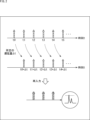
- FIG. 2 shows a pixel signal with a certain temporal periodic pattern as an example of a pixel signal input to a certain synapse.
- the group IF 31 can give a predetermined delay amount ⁇ t to a pixel signal input to a certain product-sum unit 33 and re-input it to the same product-sum unit 33 .
- these pixel signals overlap that is, when the interval between the periodic patterns of the pixel signals and the delay amount ⁇ t match, the intermediate data obtained by the product-sum unit 33 will rise more easily, and the firing probability will increase. Become.
- the neural network processor 13 when a pixel signal is re-inputted with a delay amount ⁇ t that roughly matches the periodic pattern of the pixel signal inputted to a certain neuron, the instantaneous amount of input to that neuron increases. It will be visible. As a result, the firing probability increases, and an accompanying enhancement of the learning signal can be observed.
- the neural network processor 13 can easily detect pixel signals with a certain temporal periodic pattern, such as blinking signals or flickering light sources, and transmits the detection of such pixel signals to the image sensor 12. be able to. Note that there is a concern that the process of re-inputting pixel signals may cause excessive input to the product-sum unit 33, but by controlling the input amount as described above, excessive input to the product-sum unit 33 can be avoided. It can also be resolved efficiently.
- the neural network processor 13 can detect a predetermined spatial pattern shown in the image captured by the image sensor 12 as a region of interest based on a heat map that maps the firing rate of active neurons.
- FIG. 3 shows an example of a process in which "human eyes" captured in an image captured by the image sensor 12 are detected as a region of interest, and the region of interest is tracked.
- the solid arrows shown in FIG. 3 represent areas where input from the image sensor 12 is active, and neurons in the first layer are bidirectionally connected to the surroundings including recursive connections, and neurons in the second layer are connected bidirectionally to the surroundings including recursive connections. Neurons are bi-directionally fully connected between layers.
- the neurons N in the first layer act to repeat recursive inputs to maintain firing around areas with many inputs.
- the neurons N in the second layer suppress the firing maintenance effect of the neurons N in the first layer as the overall firing rate increases, and have the same effect as noise removal.
- the area where the heat map is active is set as a region-of-interest (RoI), and sensor output outside this area is suppressed.
- RoI region-of-interest
- the region of interest by placing pixels outside the area of interest in a standby state, power etc. can be reduced. It can be made more efficient. That is, based on the information that the region of interest has a high number of neuron firings, it is possible to control the presence or absence of output for each pixel 21, or to control the presence or absence of output for each pixel group 22.
- the input from the pixel signals output from the 5th to 9th pixels is active according to the attention area
- the input from the pixel signals output from the 5th to 9th pixels is active according to the attention area after movement.
- Inputs from pixel signals output from the 8th to 12th pixels are active, and the region of interest can be determined or changed (tracked). Then, pixels other than the eye area can be placed in a standby state.
- FIG. 3 only shows a network in one axis direction for convenience, the neural network processor 13 implements a network in two axis directions, and is capable of tracking the region of interest two-dimensionally. can.
- FIG. 3 the neural network model (Attractor) in FIG. 3 (the same applies to FIGS. 17 and 24 described later) is illustrated more accurately, it has a structure as shown in FIG. 4.
- FIG. 4A shows a neural network model using only the first layer.
- connections from all neurons N to several peripherals of each neuron N are configured by "inputs” or “inverting inputs.” Further, the connection may be configured using only one of the input types of "input” and "inverted input”.
- connections extending from neuron N indicated by a solid line to neuron N indicated by a broken line are emphasized, and in reality, connections extend from all neurons N. However, due to the complexity, it is omitted from the illustration.
- FIG. 4B shows a neural network model using the first and second layers.
- the connection pattern is similar to the configuration shown in A of FIG. 4, and here, it may be configured with only positive inputs or mixed with inverted inputs.
- weights are set respectively so that the connection from the first layer to the second layer is positive, and the connection from the second layer to the first layer is reversed. be done.
- These connections include a configuration in which the connections are fully connected, a configuration in which connections are stochastically thinned out from the total connection, and a configuration in which neurons N spatially adjacent to the first layer are locally connected (see B in Figure 4).
- the solid line neurons N in the second layer are shown to be connected only to the neighboring solid line neurons N in the first layer, but each neuron N in the second layer and all neurons N in the first layer are connected to each other. It may be a combination or a probabilistic full combination.
- a mechanism for transmitting information from the neural network processor 13 to the image sensor 12 will be described with reference to FIGS. 5 and 6.
- the neural network processor 13 unrolls a plurality of neurons N in the time direction (unrolled model), acquires the value of learning information obtained by each neuron N at every time step, and stores it. can do.
- FIG. 6A shows an example of processing for accumulating learning information for each pixel 21.
- information is transmitted to the learning unit 38 at a ratio of k neurons N that are the output side to one pixel 21 that is the input side, and the learning unit 38 performs learning according to the ratio of the output to the input. Form information. Then, the learning unit 38 sequentially supplies this learning information to the learning memory 42 and adds it for each pixel 21. Thereafter, the group IF 31 transmits the learning information accumulated in the learning memory 42 for each pixel 21 of the image sensor 12 at a predetermined time.
- FIG. 6B shows an example of processing for accumulating learning information for each pixel group 22.
- information is transmitted to the learning unit 38 at a ratio of n ⁇ k neurons N serving as the output side to n pixels 21 serving as the input side, and the learning unit 38 responds to the ratio of output to input. form learning information. Then, the learning unit 38 sequentially supplies this learning information to the learning memory 42 and adds all the pixels 21 into one without dividing them.
- the group IF 31 transmits the learning information stored in the learning memory 42 to the corresponding pixel group 22 of the image sensor 12 at a predetermined time.
- the neural network processor 13 can accumulate learning information for each pixel 21 or pixel group 22 and transmit information based on the learning information to the image sensor 12 side.
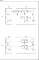
- a first connection configuration example shown in A of FIG. 7 is a connection configuration in which the neural network processor 13 includes one input/output IF 40 and a plurality of group IFs 31 are connected to the image sensor 12 via the input/output IF 40. It has become. Therefore, data is transmitted and received with the image sensor 12 via the input/output IF 40, and the input/output IF 40 distributes the data transmitted from the image sensor 12 to the corresponding group IF 31.
- connection configuration example shown in FIG. 7B is a connection configuration in which the pixel group 22 and the neuron group 39 are connected via the group IF 31 in a one-to-one correspondence.
- the third connection configuration example shown in FIG. 8 has a connection configuration in which group IFs 31 are connected in a hierarchical structure.
- group IFs 31 are connected in a hierarchical structure.
- a plurality of lower group IFs 31D are connected to an upper group IF 31U
- a plurality of upper group IFs 31U are connected to the image sensor 12 via an input/output IF 40.
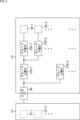
- the image sensor 12 is configured such that a pixel array section 51 is connected to an input/output IF 54 via a pixel control section 52 and a pixel output control section 53.
- the neural network processor 13 is connected to the group IF 31 in a connection configuration as shown in A of FIG.
- the pixel control unit 52 controls the characteristics of the pixels 21 arranged in an array in the pixel array unit 51 and the area of interest captured in the image captured by the image sensor 12. For example, the characteristics of the pixel 21 are determined by a bias value or the like.
- the pixel control unit 52 also caches and manages registers that determine pixel characteristics. For example, the characteristics of the pixel 21 include sensitivity, response speed, noise amount, and the like.
- the pixel output control section 53 performs controls such as rasterizing and outputting the data of the pixel array section 51. Further, the pixel output control section 53 may perform preprocessing of the output data, or a block (not shown) connected to the pixel output control section 53 may perform preprocessing of the output data. For example, preprocessing includes denoising, adjusting gain or output amount, removing flicker, and the like.
- the control content for the image sensor 12 is determined based on the processing result of the processing performed in the neural network processor 13. For example, based on the above-mentioned learning signal, the pixel control unit 52 adjusts the characteristics of the pixel 21 (for example, one or more of gain, delay, noise, and refractory period), controls the region of interest ( For example, the region of interest can be determined or changed and pixels other than the region of interest can be placed in a standby state, or the pixel output control unit 53 can change parameters such as preprocessing.
- the characteristics of the pixel 21 for example, one or more of gain, delay, noise, and refractory period
- the region of interest can be determined or changed and pixels other than the region of interest can be placed in a standby state, or the pixel output control unit 53 can change parameters such as preprocessing.
- a configuration may be adopted in which the neural network processor 13 is mounted inside the image sensor 12.
- the neural network processor 13 is connected to the group IF 31 in a connection configuration as shown in FIG. 7B.
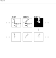
- the solid-state image sensor 11 can output only the necessary area by switching the output-driven pixels 21 according to the firing frequency of neurons.
- the upper part of FIG. 11 shows an example of the image at each time output from the image sensor 12, and the lower part of FIG. 11 shows a map of the firing rate of active neurons obtained from the image at each time.
- An example of a heat map is shown.
- the necessary area at time T3 is learned from the heat map at time T1 and time T2, and an image of only the necessary area, that is, an image with pixels 21 other than the necessary area in a non-driving state (standby state) is created at time T3. will be output.
- the solid-state image sensor 11 can improve the efficiency of power consumption by outputting only the necessary area.
- the state transition of the pixel 21 may take time.
- the solid-state image sensor 11 controls the driving so that the pixels 21 in the transition waiting state temporarily stop updating the state and hold the state, and the pixels 21 other than the transition waiting state continue processing. Then, based on the change in the firing rate of the neuron, that is, based on the frequency differentiation (or information equivalent to the frequency differentiation), it predicts which pixels will require a state transition at the next time.
- the pixels 21 to start driving can be prepared in advance.
- a learning signal With reference to FIG. 12, the formation of a learning signal will be described as a first example of an operation corresponding to frequency differentiation.
- the LI unit 35 issues a signal (+1) when the cumulative leakage value ⁇ of the number of firings shown in A in FIG. -1) is issued.
- the firing unit 36 sends a signal when the value v of the membrane potential shown in B in FIG. 12 and the cumulative leakage value ⁇ of the number of firings shown in A in FIG. ( ⁇ 1) is issued.
- a learning scheme such as the first scheme or the second scheme is adopted, and the signal is incremented for a predetermined time by the group IF 31, and this value is used as a learning signal.
- control for the pixel 21 is started.
- flow estimation of the firing rate of a neuron will be described as a second example of the calculation equivalent to frequency differentiation.
- the direction from the left to the right of the neuron N shown in FIG. 13 is assumed to be the positive direction. Then, when the timing of a signal from a certain neuron N and a signal arriving with a predetermined delay from the neuron N next to the left of the positive neuron N overlaps, the firing rate of that positive neuron N increases. do. In other words, forward direction can be replaced with firing rate.
- the movement of the neuron heat map is predicted and the next time
- the pixels 21 in the high firing region can be driven in advance.
- the image sensor 12 when a region of interest is output from the image sensor 12 and input to the neural network processor 13, a calculation is performed to recognize a subject appearing in the region of interest, and the calculation is performed. Depending on the result, the image sensor 12 can be notified of the next time's attention area. Thereby, in the solid-state image sensor 11, the region of interest that the image sensor 12 outputs at the next time can be changed.
- Example of network configuration A network configuration employed in the solid-state image sensor 11 will be described with reference to FIGS. 14 to 19. Note that the network configuration described here is an example, and the solid-state image sensor 11 is not limited to this example, and may adopt other network configurations.
- the solid-state image sensor 11 is configured such that the pixels 21 included in the pixel group 22 overlap and the neurons N included in the neuron group 39 overlap.
- pixel 21-3 among pixels 21-1 to 21-5 is connected to group IFs 31-1 and 31-2, respectively
- neuron N-3 among neurons N-1 to N-5 is , are connected to group IFs 31-1 and 31-2, respectively. Therefore, the pixel 21-3 is included in two pixel groups 22, and the neuron N-3 is included in two neuron groups 39, which are configured to overlap in each group.
- weights ⁇ 0 to ⁇ 3 shown in FIG. 14 indicate the weights of a weighted convolution operation (convolution), and FIG. 14 is an example of the convolution operation.
- the solid-state image sensor 11 may have a network configuration (not shown) in which it is connected to the group IF 31 so that the arrangement of the pixels 21 does not overlap. Further, the solid-state image sensor 11 may have a network configuration (not shown) in which the array of pixels 21 is fully connected to the group IF 31.
- the solid-state image sensor 11 is configured to include one or more layers of neural network circuits 61 between the array of pixels 21 and the group IF 31. That is, the pixel signals output from the pixels 21-1 to 21-5 are input to the neural network circuit 61, and the predicted pixels 62-1 to 62-5 of the predicted image output from the neural network circuit 61 are grouped into the group IF 31-1. and 31-2, respectively.
- the solid-state image sensor 11 is configured such that a pixel conversion circuit 63 is disposed between the array of pixels 21 and the group IF 31.
- the pixel conversion circuit 63 converts the value of the analog signal (potential or current) output from the pixel 21 into a digital value or binary value using an AD (Analog-Digital) converter or the like, and converts the value of the analog signal (potential or current) output from the pixel 21 into a digital value or a binary value, and converts it into a digital value or a binary value. Enter -2.
- the solid-state image sensor 11 has a convolution layer 64 arranged between the array of pixels 21 and a plurality of group IFs 65 (an interface composed of a plurality of group IFs 31).
- the convolution layer 64 may be a network that combines operations including a plurality of convolution operations.
- the group neuron 66 connected to the multiple group IF 65 is configured with one type of weighted operation such as Attractor, Convolution, Fully Connection, or Self-Attention, or configured with a combination of multiple weighted operations. It's okay.
- the group neuron 66 may be configured with operations other than those exemplified here.
- the structure of the neural network model (Attractor) shown in the group neuron 66 is the structure shown in FIG. 4 described above to be more accurately illustrated.
- Group addressing will be explained with reference to FIGS. 20 to 23.
- the solid-state image sensor 11 in order to simplify learning and pixel control, and to reduce the scale of the control circuit, it is efficient to group a plurality of pixels 21 and a plurality of neurons N by associating them with each other.
- the communication of both the image sensor 12 and the neural network processor 13 takes place through this group, ie via the group address.
- controllability of the region of interest is improved, and address changes on the neural network processor 13 side corresponding to changes in the address of the region of interest on the image sensor 12 side can be exchanged using a small number of bits. becomes possible.
- FIG. 20 For example, as shown in A of FIG. 20, an example will be described in which a small size attention area is changed to a large size attention area.
- the address is changed from the pixel group 22 to the neuron group 39, as shown in FIG. 20B.
- the address lines indicated by broken lines in D in FIG. 20 indicate that they are not used in small-sized attention areas, and address lines G0 to G2 are used in small-sized attention areas. Then, the address is manipulated in accordance with the change to a larger size area of interest, and address lines G0' to G4' are used. Note that D in FIG. 20 assumes an addressing/access circuit using content addressable memory (CAM), but addresses can be changed in the same way even with soft memory.
- CAM content addressable memory
- FIG. 21 is a block diagram showing a configuration example of the neural network processor 13 including the address control circuit 71.
- the neural network processor 13 is configured to include an address control circuit 71 connected to the group IF 31, and the address control circuit 71 is provided with a storage section 72.
- the storage unit 72 stores a virtual address table 73 that is rewritten according to notifications from the image sensor 12.
- the address control circuit 71 refers to the virtual address table 73 stored in the storage unit 72 and performs address conversion processing to change the address on the neuron N side.
- FIG. 22 is a diagram illustrating address conversion processing by the address control circuit 71.
- the image sensor 12 supplies the RoI change notification, address pattern, group address, and data to the neural network processor 13.
- the address control circuit 71 determines to change the address in accordance with the RoI change notification, performs an address replacement operation based on the group address pattern table and the address table, and outputs the changed address. Then, by integrating the group address supplied from the image sensor 12 and the changed address output from the address control circuit 71, the physical address of each neuron N in the neuron group 39 is specified. That is, by changing the virtual address of the neuron group 39 corresponding to the changed pixel group 22, the pixel group 22 and the neuron group 39 are newly associated.
- FIG. 23 is a diagram illustrating an example of an RoI change notification.
- the data when a rasterized group is input, the data is rearranged to match the arrangement of neurons, and then thinned out.
- information for zero padding is input from the image sensor 12 to the neural network processor 13.
- FIG. 24 is a diagram illustrating a network for post-processing. Note that the structure of the neural network model (Attractor) shown in FIG. 24 is the structure shown in FIG. 4 described above to be more accurately illustrated.
- networks for tracking the region of interest are provided in a stacked manner inside the solid-state image sensor 11 so as to be directly connected to the pixels 21.
- wiring is provided so as to be stacked via a Cu-Cu bond, and the neural network processor 13 side of this bonding surface is Group IF 31 is arranged in .
- a neural network circuit 91 for post-processing is provided outside the solid-state image sensor 11, and both the neural network processor 13 and the neural network circuit 91 for post-processing communicate with each other, and the image sensor 12 and Both can communicate with the neural network circuit 91 for post-processing.
- the outside of the solid-state image sensor 11 refers to a destination where the serialized output of the pixel 21 is communicated through a predetermined wiring such as a bus. Therefore, whether the neural network circuit 91 for post-processing is provided inside the solid-state image sensor 11 or outside the solid-state image sensor 11, as long as it is provided at the end of such communication, It may be.
- the output value of the neural network circuit 91 for post-processing may be a vector value indicating the line-of-sight direction.
- the address control circuit 71 shown in FIG. 21 described above is connected to the input stage group IF 31.
- the neural network circuit 91 for tracking the attention area shown in FIG. 24 By mutually communicating with the neural network circuit 91 for tracking the attention area shown in FIG. 24, it is possible to communicate the reliability of the attention area, for example, and improve the accuracy of tracking the attention area.
- a signal having an intensity in the form of a point spread function centered on the center of gravity of the region of interest may be defined and notified.
- the configuration in which the neural network processor 13 is provided inside the solid-state image sensor 11 and the neural network circuit 91 for post-processing is provided outside the solid-state image sensor 11, that is, the configuration in which they are arranged separately, has the purpose. It is preferable to use the appropriate one depending on the network used.
- all pixel groups 22 and all neuron groups 39 are associated with each other, as shown in FIG. 7B above. It is preferable to adopt a configuration that provides quick response and reduces power consumption. In other words, with such a configuration, the amount of data handled by each group IF 31 is relatively reduced, and congestion (waiting time) associated with data transmission and reception can be reduced. Furthermore, by employing such a laminated structure, the signal transmission distance between the pixel 21 and the neuron N can be shortened, so it is possible to expect an improvement in processing speed and a reduction in power consumption.
- a neural network circuit 91 for post-processing and perform a predetermined output outside the solid-state image sensor 11. processing can be performed flexibly.
- the configuration in which the neural network processor 13 is disposed all over the bottom of the image sensor 12 and the pixels 21 and the group IF 31 are connected to each other means that some pixels 21 are not used and the wiring This is because there will be a lot of waste.
- the neural network circuit 91 regardless of whether it is inside or outside the solid-state image sensor 11, as long as it is outside the pixel 21, the neural network circuit 91 only has to be arranged on a necessary scale, which is efficient in terms of footprint and the like.
- the neural network processor 13 is not limited to the configuration including the input/output IF 40 as shown in FIG. 7A.
- a neural network circuit 91 using a general-purpose GPU performs advanced processing, and all pixel groups 22 and all neuron groups 39 correspond to each other, as shown in FIG. 7B above.
- the neural network processor 13 having the above configuration may be responsible for lightweight and high-speed processing.
- first network and the second network in combination, it is possible to optimize the processing division of the entire system (for example, adjustment of processing speed and power). Further, calculations can be performed while performing communication and control between the pixel 21 and the first network and the second network, and communication and control between the first network and the second network, as described above. We can expect further optimization of processing division and accuracy.
- a solid-state image sensor that captures images (RGB images or brightness images)
- the present technology is not limited to solid-state image sensors and can be applied to various light detection devices. be able to.
- this technology uses sensors that use Photon-Count SPAD (Single Photon Avalanche Diode), EVS (Event-based Vision Sensor) that detects the occurrence of events, TOF (Time Of Flight) sensors that measure distance, and multiple It can be applied to various photodetection devices, such as multispectral sensors that acquire multispectral images of wavelengths.
- the present technology may be applied to photodetecting devices other than these.
- the solid-state image sensor 11 as described above is applied to various electronic devices such as an imaging system such as a digital still camera or a digital video camera, a mobile phone equipped with an imaging function, or other equipment equipped with an imaging function. be able to.
- an imaging system such as a digital still camera or a digital video camera
- a mobile phone equipped with an imaging function or other equipment equipped with an imaging function. be able to.
- FIG. 25 is a block diagram showing an example of the configuration of an imaging device installed in an electronic device.
- the imaging device 101 includes an optical system 102, an image sensor 103, a signal processing circuit 104, a monitor 105, and a memory 106, and is capable of capturing still images and moving images.
- the optical system 102 is configured with one or more lenses, guides image light (incident light) from the subject to the image sensor 103, and forms an image on the light-receiving surface (sensor section) of the image sensor 103.
- the solid-state image sensor 11 described above is applied as the image sensor 103. Electrons are accumulated in the image sensor 103 for a certain period of time depending on the image formed on the light-receiving surface via the optical system 102. A signal corresponding to the electrons accumulated in the image sensor 103 is then supplied to the signal processing circuit 104.
- the signal processing circuit 104 performs various signal processing on the pixel signals output from the image sensor 103.
- An image (image data) obtained by signal processing performed by the signal processing circuit 104 is supplied to a monitor 105 for display, or supplied to a memory 106 for storage (recording).
- the imaging device 101 configured in this way, by applying the above-described solid-state imaging device 11, for example, it is possible to efficiently process a captured image.
- FIG. 26 is a diagram showing an example of use of the above-described image sensor (imaging device).
- the above-described image sensor can be used in various cases for sensing light such as visible light, infrared light, ultraviolet light, and X-rays, for example, as described below.
- ⁇ Digital cameras, mobile devices with camera functions, and other devices that take images for viewing purposes Devices used for transportation, such as in-vehicle sensors that take pictures of the rear, surroundings, and interior of the car, surveillance cameras that monitor moving vehicles and roads, and distance sensors that measure the distance between vehicles, etc.
- Devices used for transportation such as in-vehicle sensors that take pictures of the rear, surroundings, and interior of the car, surveillance cameras that monitor moving vehicles and roads, and distance sensors that measure the distance between vehicles, etc.
- User gestures Devices used in home appliances such as TVs, refrigerators, and air conditioners to take pictures and operate devices according to the gestures.
- - Endoscopes devices that perform blood vessel imaging by receiving infrared light, etc.
- Devices used for medical and healthcare purposes - Devices used for security, such as surveillance cameras for crime prevention and cameras for person authentication - Skin measurement devices that take pictures of the skin, and devices that take pictures of the scalp - Devices used for beauty purposes, such as microscopes for skin care.
- - Devices used for sports such as action cameras and wearable cameras.
- - Cameras, etc. used to monitor the condition of fields and crops. , equipment used for agricultural purposes
- the present technology can also have the following configuration.
- an image sensor provided with a pixel group consisting of N (N is a positive integer) pixels among a plurality of pixels arranged in an array on a sensor surface; a processor in which a neural network is configured by a neuron group having M (M is a positive integer) neurons; a group interface provided between the pixel group and the neuron group and performing bidirectional communication between the image sensor and the processor.
- the photodetection device further comprising: a pixel control unit that uses a processing result of the processing performed in the neural network to control characteristics of the pixel.
- a firing detection unit detects firing of a neuron that exceeds the threshold; a learning section that determines a learning signal based on the firing rate of the neuron detected by the firing detection section; further comprising a learning memory that accumulates the learning signal output from the learning unit over time,
- the photodetection device according to any one of (2) to (5) above, wherein a value obtained by accumulating the learning signal in the learning memory is supplied to the pixel control unit as a control signal and used to control the characteristics of the pixel.
- the photodetection device further comprising: a calculation unit that performs differentiation of the firing rate of the neuron or calculation equivalent to the differentiation, and supplies the calculation result to the firing detection unit.
- a calculation unit that performs differentiation of the firing rate of the neuron or calculation equivalent to the differentiation, and supplies the calculation result to the firing detection unit.
- the calculation unit performs calculation corresponding to the differentiation using at least one of the leakage integral value of the firing number of the neuron and the membrane potential.
- the calculation unit calculates a temporal movement rate of the firing rate, which is a spatial differentiation of the spatial distribution of the firing rate of the neuron, by a calculation corresponding to the differentiation.
- a neural network circuit other than the processor is connected to the outside of the photodetection device, and both the processor and the neural network circuit other than the processor communicate with each other, and the image sensor and the neural network circuit other than the processor communicate with each other.
- the photodetection device according to any one of (1) to (13) above, wherein both communicate.
- the processor When the region of interest is output from the image sensor and input to the processor, the processor performs a calculation to recognize a subject appearing in the region of interest, and adjusts the region of interest at the next time to the image according to the result of the calculation.
- the photodetection device according to (5) above, wherein the area of interest that the image sensor outputs at the next time is changed by notifying the sensor.
- an image sensor provided with a pixel group consisting of N (N is a positive integer) pixels among a plurality of pixels arranged in an array on a sensor surface; a processor in which a neural network is configured by a neuron group having M (M is a positive integer) neurons;
- An electronic device comprising: a group interface that is provided between the pixel group and the neuron group and performs bidirectional communication between the image sensor and the processor.
- Solid-state image sensor 12 Image sensor, 13 Neural network processor, 21 Pixel, 22 Pixel group, 31 Group IF, 32 Storage unit, 33 Product-sum unit, 34 Memory, 35 LI unit, 36 Firing unit, 37 neuron control unit, 38 learning unit, 39 neuron group, 40 input/output IF, 41 input buffer, 42 learning memory, 51 pixel array section, 52 pixel control section, 53 pixel output control section, 54 input/output IF, 61 neural network circuit, 62 Predicted pixel , 63 Pixel conversion circuit, 64 Convolution layer, 65 Multiple group IF, 66 Group neuron, 67 Full contact layer, 68 Down sample layer, 71 Address control circuit, 72 Storage unit, 73 Virtual address table, 91 Neural network for post-processing circuit
Landscapes
- Engineering & Computer Science (AREA)
- Physics & Mathematics (AREA)
- Theoretical Computer Science (AREA)
- General Physics & Mathematics (AREA)
- Health & Medical Sciences (AREA)
- Life Sciences & Earth Sciences (AREA)
- Biomedical Technology (AREA)
- Biophysics (AREA)
- Computing Systems (AREA)
- Artificial Intelligence (AREA)
- General Health & Medical Sciences (AREA)
- Molecular Biology (AREA)
- Data Mining & Analysis (AREA)
- General Engineering & Computer Science (AREA)
- Computational Linguistics (AREA)
- Mathematical Physics (AREA)
- Software Systems (AREA)
- Evolutionary Computation (AREA)
- Power Engineering (AREA)
- Signal Processing (AREA)
- Neurology (AREA)
- Electromagnetism (AREA)
- Condensed Matter Physics & Semiconductors (AREA)
- Multimedia (AREA)
- Computer Hardware Design (AREA)
- Microelectronics & Electronic Packaging (AREA)
- Image Analysis (AREA)
Abstract
La présente divulgation concerne un dispositif de détection de lumière et un instrument électronique qui permettent d'améliorer l'efficacité. Dans la présente divulgation, une interface de groupe est disposée entre : un capteur d'image dans lequel un groupe de pixels est constitué de N pixels parmi une pluralité de pixels agencés selon une forme de réseau sur une surface de capteur ; et un processeur dans lequel un réseau neuronal est configuré à partir d'un groupe de neurones ayant M neurones. Par l'intermédiaire de cette interface de groupe, une communication bidirectionnelle est effectuée entre le capteur d'image et le processeur. La présente technologie est applicable à des capteurs d'image CMOS du type empilé, par exemple.
Applications Claiming Priority (2)
| Application Number | Priority Date | Filing Date | Title |
|---|---|---|---|
| JP2022-035042 | 2022-03-08 | ||
| JP2022035042 | 2022-03-08 |
Publications (1)
| Publication Number | Publication Date |
|---|---|
| WO2023171333A1 true WO2023171333A1 (fr) | 2023-09-14 |
Family
ID=87936896
Family Applications (1)
| Application Number | Title | Priority Date | Filing Date |
|---|---|---|---|
| PCT/JP2023/005917 WO2023171333A1 (fr) | 2022-03-08 | 2023-02-20 | Dispositif de détection de lumière et instrument électronique |
Country Status (1)
| Country | Link |
|---|---|
| WO (1) | WO2023171333A1 (fr) |
Citations (1)
| Publication number | Priority date | Publication date | Assignee | Title |
|---|---|---|---|---|
| JP2022511414A (ja) * | 2018-12-17 | 2022-01-31 | フェイスブック・テクノロジーズ・リミテッド・ライアビリティ・カンパニー | 動的にプログラム可能な画像センサ |
-
2023
- 2023-02-20 WO PCT/JP2023/005917 patent/WO2023171333A1/fr unknown
Patent Citations (1)
| Publication number | Priority date | Publication date | Assignee | Title |
|---|---|---|---|---|
| JP2022511414A (ja) * | 2018-12-17 | 2022-01-31 | フェイスブック・テクノロジーズ・リミテッド・ライアビリティ・カンパニー | 動的にプログラム可能な画像センサ |
Similar Documents
| Publication | Publication Date | Title |
|---|---|---|
| US11265467B2 (en) | System and apparatus for co-registration and correlation between multi-modal imagery and method for same | |
| US20180077374A1 (en) | Image sensor, processing method, and electronic apparatus | |
| US11037968B2 (en) | Image sensor architecture | |
| KR20210052444A (ko) | 촬상 장치, 촬상 시스템, 촬상 방법 및 촬상 프로그램 | |
| US20180227514A1 (en) | Image sensor and electronic apparatus | |
| US10761182B2 (en) | Star tracker for multiple-mode detection and tracking of dim targets | |
| US20200372254A1 (en) | Method for outputting a signal from an event-based sensor, and event-based sensor using such method | |
| US20170358614A1 (en) | Solid-state imaging device and electronic apparatus | |
| US20220076402A1 (en) | High bandwidth camera data transmission | |
| US20210218923A1 (en) | Solid-state imaging device and electronic device | |
| CN109640011A (zh) | 固态成像设备和成像系统 | |
| WO2020155739A1 (fr) | Capteur d'image, procédé d'acquisition de données d'image à partir d'un capteur d'image, et dispositif de caméra | |
| EP3512193B1 (fr) | Élément d'imagerie et procédé d'excitation et appareil électronique | |
| JP2016143851A (ja) | 固体撮像素子、および電子装置 | |
| KR102604317B1 (ko) | 촬상 소자, 촬상 방법 및 전자 기기 | |
| WO2019035369A1 (fr) | Dispositif d'imagerie à semi-conducteurs et procédé de commande associé | |
| WO2023171333A1 (fr) | Dispositif de détection de lumière et instrument électronique | |
| US20230152890A1 (en) | Imaging display device and wearable device | |
| US20180160064A1 (en) | Solid-state imaging device and electronic apparatus | |
| US10602071B2 (en) | Imaging device and control method | |
| KR101685419B1 (ko) | 디지털 영상 처리 장치 및 방법 | |
| US20240031691A1 (en) | Imaging element and imaging device | |
| US20240080573A1 (en) | In-plane preprocessor and multiplane hardware neural network | |
| Rizk et al. | High-performance, event-driven, low-cost, and SWaP imaging sensor for hostile fire detection, homeland protection, and border security | |
| US11048465B2 (en) | Imaging display device, wearable device, and imaging display system |
Legal Events
| Date | Code | Title | Description |
|---|---|---|---|
| 121 | Ep: the epo has been informed by wipo that ep was designated in this application |
Ref document number: 23766512 Country of ref document: EP Kind code of ref document: A1 |