WO2023171033A1 - Ferrule and optical connection structure - Google Patents
Ferrule and optical connection structure Download PDFInfo
- Publication number
- WO2023171033A1 WO2023171033A1 PCT/JP2022/040960 JP2022040960W WO2023171033A1 WO 2023171033 A1 WO2023171033 A1 WO 2023171033A1 JP 2022040960 W JP2022040960 W JP 2022040960W WO 2023171033 A1 WO2023171033 A1 WO 2023171033A1
- Authority
- WO
- WIPO (PCT)
- Prior art keywords
- ferrule
- receptacle
- optical
- longitudinal direction
- longitudinal
- Prior art date
Links
Images


Classifications
-
- G—PHYSICS
- G02—OPTICS
- G02B—OPTICAL ELEMENTS, SYSTEMS OR APPARATUS
- G02B6/00—Light guides; Structural details of arrangements comprising light guides and other optical elements, e.g. couplings
- G02B6/24—Coupling light guides
- G02B6/26—Optical coupling means
- G02B6/32—Optical coupling means having lens focusing means positioned between opposed fibre ends
-
- G—PHYSICS
- G02—OPTICS
- G02B—OPTICAL ELEMENTS, SYSTEMS OR APPARATUS
- G02B6/00—Light guides; Structural details of arrangements comprising light guides and other optical elements, e.g. couplings
- G02B6/24—Coupling light guides
- G02B6/36—Mechanical coupling means
-
- G—PHYSICS
- G02—OPTICS
- G02B—OPTICAL ELEMENTS, SYSTEMS OR APPARATUS
- G02B6/00—Light guides; Structural details of arrangements comprising light guides and other optical elements, e.g. couplings
- G02B6/24—Coupling light guides
- G02B6/42—Coupling light guides with opto-electronic elements
Definitions
- the present invention relates to a ferrule and an optical connection structure.
- Patent Document 1 discloses an optical connection structure for connecting an optical element and an optical fiber.
- positioning of the optical connector in a direction perpendicular to the longitudinal direction of the optical fiber is performed using positioning pins. Further, the positioning of the optical connector in the longitudinal direction is performed by abutting the ferrule of the optical connector against the adapter.
- the outer dimensions of the ferrule are increased by the thickness of the pin. If positioning is performed using the outer shape of the ferrule without using pins, the ferrule can be made smaller.
- the inventors of the present invention have investigated that when positioning the ferrule without using pins, the arrangement of the reference plane that serves as a reference for the ferrule position in the longitudinal direction affects the quality of the optical connection using the optical connector. It was found that
- the present invention was made in consideration of these circumstances, and an object of the present invention is to provide a ferrule and an optical connection structure that can stabilize the quality of optical connections when positioning is performed without using pins.
- a ferrule according to one aspect of the present invention is a ferrule that is connected to a receptacle fixed to an optical integrated circuit, and includes a fiber hole into which an optical fiber is inserted, and a fiber hole through which the optical fiber is inserted. and a longitudinal reference surface that determines the position of the ferrule with respect to the receptacle in the longitudinal direction of the optical fiber, and the longitudinal reference surface determines the position of the ferrule in the longitudinal direction of the optical fiber. It is located between the center line passing through the center position and the light exit surface.
- the optical connection structure includes the ferrule, the receptacle, and a holding member that holds the ferrule and the receptacle in a positioned state, and the ferrule is arranged in the longitudinal direction.
- the holding member has a pressure-receiving surface that receives a biasing force in a direction intersecting with the pressure-receiving surface, and a sliding surface that is arranged apart from the pressure-receiving surface and slides on the receptacle, and the holding member applies the biasing force to the pressure-receiving surface.
- the receptacle has a receptacle-side sliding surface that slides on the sliding surface, and the receptacle-side sliding surface has a recess into which a portion of the ferrule can enter. and when the direction in which light is emitted from the light emitting surface in the longitudinal direction is the forward direction, an inclined surface is formed inside the recessed portion such that the inclined surface approaches the receptacle side sliding surface toward the front. ing.
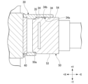
- FIG. 2 is a diagram showing an optical connection structure according to the present embodiment.
- 2 is a perspective view showing the vicinity of one optical connection unit in FIG. 1.
- FIG. FIG. 3 is an exploded perspective view of FIG. 2;
- FIG. 3B is a perspective view of the vicinity of the receptacle in FIG. 3A viewed from below.
- FIG. 3B is a perspective view of the optical connector of FIG. 3A viewed from the front.
- FIG. 2 is a schematic diagram illustrating the transmission of light between an optical fiber and an optical integrated circuit in this embodiment.
- FIG. 3 is a cross-sectional view taken along the line VV in FIG. 2; 3 is a cross-sectional view taken along the line VI-VI in FIG. 2;
- FIG. 7A is a diagram showing a state subsequent to FIG. 7A.
- FIG. FIG. 7B is a diagram showing a state following FIG. 7B.
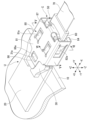
- the optical connection structure 1 includes a substrate 10 and a plurality of optical connection units U.
- each optical connection unit U includes an optical integrated circuit 20, a receptacle 30, a microlens array 40, an optical connector C, and a holding member 80.
- the optical connector C includes a ferrule 50, a boot 60, and a tape core wire 70.
- the ferrule 50 is formed with a plurality of fiber holes 51 (see FIGS. 4 and 6) into which a plurality of optical fibers F can be inserted.
- the plurality of fiber holes 51 are arranged along one direction orthogonal to the longitudinal direction of each fiber hole 51.
- an XYZ orthogonal coordinate system is set to explain the positional relationship of each component.
- the X-axis direction is a direction along the longitudinal direction of each fiber hole 51.
- the Y-axis direction is the direction in which the plurality of fiber holes 51 are arranged.
- the Z-axis direction is a direction perpendicular to both the X-axis and the Y-axis.
- the X-axis direction is sometimes referred to as the longitudinal direction X
- the Y-axis direction is sometimes referred to as the first direction Y
- the Z-axis direction is sometimes referred to as the second direction Z.
- the direction from the ferrule 50 toward the optical integrated circuit 20 along the longitudinal direction X is referred to as the +X side or the front.
- the direction opposite to the +X side is referred to as the -X side or rearward.
- One direction along the first direction Y is referred to as the +Y side or the left side.
- the direction opposite to the +Y side is called the -Y side or right side.
- the direction from the substrate 10 toward the optical integrated circuit 20 along the second direction Z is referred to as the +Z side or upward.
- the direction opposite to the +Z side is referred to as the -Z side or downward direction.
- the tape core wire 70 is configured by covering a plurality of optical fibers F together or by intermittently fixing each other.
- the plurality of optical fibers F may not constitute the ribbon cable 70, and each optical fiber F may be individually coated.
- the boot 60 has a cylindrical shape extending in the longitudinal direction X, and the tape core wire 70 is inserted into the boot 60.
- the boot 60 is made of an elastic material and extends from the ferrule 50 toward the ⁇ X side.
- the boot 60 has the role of alleviating bending and stress applied to the optical fiber F.
- electronic components 11 are mounted on the upper surface of the board 10. Furthermore, a circuit pattern (not shown) electrically connected to the electronic component 11 is formed on the substrate 10.
- the electronic component 11 may be, for example, a switch circuit.
- the plurality of optical connection units U are arranged so as to surround the electronic component 11.
- the optical integrated circuit 20 is mounted on the upper surface of the substrate 10.
- the optical integrated circuit 20 is formed into a rectangular parallelepiped shape.
- the optical integrated circuit 20 includes a light receiving element (not shown) that converts an optical signal into an electrical signal, and a light emitting element (not shown) that converts the electrical signal into an optical signal.
- a light receiving element for example, a photodetector such as a photodiode can be used.
- As the light emitting element for example, a semiconductor laser, a light emitting diode, etc. can be used.
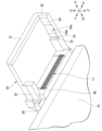
- the optical integrated circuit 20, the microlens array 40, and the receptacle 30 are fixed to each other with an adhesive.
- the front surface (+X side end surface) of the microlens array 40 may be adhesively fixed to the rear surface ( ⁇ X side end surface) of the optical integrated circuit 20.
- the adhesive is preferably a material that transmits light.
- the method of fixing the optical integrated circuit 20, the receptacle 30, and the microlens array 40 is not limited to the above, and may be changed as appropriate.
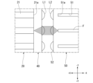
- the optical integrated circuit 20 has a plurality of waveguides 21. Note that in figures other than FIG. 4, illustration of the waveguide 21 is omitted.
- Each waveguide 21 is optically connected to the above-mentioned light receiving element and light emitting element.
- each waveguide 21 extends along the longitudinal direction X.
- Each waveguide 21 is made of silicon, for example.
- the refractive index of the waveguide 21 is higher than the refractive index of a portion of the optical integrated circuit 20 other than the waveguide 21 .
- the waveguide 21 may be provided on the surface (upper surface) of the optical integrated circuit 20 or may be provided inside the optical integrated circuit 20.
- an input/output section 21a is provided at the rear end (-X side end) of each waveguide 21, an input/output section 21a is provided.
- the input/output section 21a is a part of the waveguide 21, and receives and emits optical signals.
- an abutment surface 51a against which the +X side end of the optical fiber F abuts is formed inside the fiber hole 51 of the ferrule 50.
- the abutment surface 51a faces the ⁇ X side.
- the plurality of optical fibers F are respectively inserted into the plurality of fiber holes 51 and abutted against the respective abutting surfaces 51a of the fiber holes 51.
- the ferrule 50 has a lens forming surface 52 that faces the microlens array 40 in the longitudinal direction X.
- a plurality of lenses L2 arranged in the first direction Y are formed on the lens forming surface 52.
- the microlens array 40 is made of a material that can transmit light.
- the microlens array 40 may be formed of, for example, quartz glass or a silicon substrate.
- the shape of the microlens array 40 is a rectangular plate.
- a plurality of lenses L1 are formed in the microlens array 40.
- the ferrule 50 and the microlens array 40 face each other in the longitudinal direction X, as shown in FIG. More specifically, the plurality of lenses L2 formed on the ferrule 50 face the plurality of lenses L1 of the microlens array 40.
- the optical signal that has traveled within the optical fiber F toward the +X side enters the ferrule 50 from the abutment surface 51a of the fiber hole 51. Further, the optical signal is emitted from the lens L2 of the ferrule 50 to the +X side. That is, the surface of the lens L2 is a light exit surface from which light is emitted from the ferrule 50.
- the light emitted from the ferrule 50 enters the microlens array 40 through the lens L1. Further, the light passing through the microlens array 40 is received by the input/output section 21 a of the optical integrated circuit 20 and propagates through the waveguide 21 . The optical signal is then converted into an electrical signal by a light receiving element included in the optical integrated circuit 20 and delivered to the substrate 10. Conversely, an electrical signal transmitted from the substrate 10 to the optical integrated circuit 20 is converted into an optical signal by a light emitting element included in the optical integrated circuit 20. Then, this optical signal propagates through the waveguide 21 and is emitted toward the optical fiber F from the input/output section 21a. In this way, the optical connection structure 1 performs optical connection between the optical fiber F and the optical integrated circuit 20.
- the optical connector C is attached to the receptacle 30 and can be removed from the receptacle 30 (details will be described later).
- the receptacle 30 has the role of positioning the ferrule 50 of the optical connector C with respect to the optical integrated circuit 20.
- the receptacle 30 has a top wall 31, a first side wall 32, and a second side wall 33.
- the upper wall 31 has a plate shape extending in the first direction Y and the longitudinal direction X.
- the first side wall 32 extends from the +Y side end of the upper wall 31 toward the -Z side.
- the second side wall 33 extends from the -Y side end of the upper wall 31 toward the -Z side.
- the dimension of the second side wall 33 is shorter than the dimension of the first side wall 32.
- the first side wall 32 and the second side wall 33 are spaced apart in the first direction Y.
- the upper wall 31 is formed with a protrusion 31a that protrudes toward the +Z side.
- a locking portion 86 (described later) of the holding member 80 is locked to the protrusion 31a.
- the first side wall 32 has a receptacle-side sliding surface 34 facing the ⁇ Y side.
- a recess 34a is formed in the receptacle side sliding surface 34 and is recessed toward the +Y side.
- the receptacle side sliding surface 34 is divided into two parts separated in the longitudinal direction X by the recess 34a.
- an inclined surface 34b is formed inside the recess 34a.
- the inclined surface 34b is inclined toward the ⁇ Y side as it goes toward the +X side. In other words, the inclined surface 34b is inclined so as to approach the receptacle-side sliding surface 34 as it goes toward the +X side.
- a positioning surface 35 facing the -X side is formed on the first side wall 32.
- the positioning surface 35 is located on the +X side with respect to the receptacle side sliding surface 34.
- the positioning surface 35 has a role of determining the relative position of the receptacle 30 and the ferrule 50 in the longitudinal direction X.
- the second side wall 33 is also formed with a positioning surface located in the same plane as the positioning surface 35 of the first side wall 32 . The ferrule 50 is abutted against these two positioning surfaces.
- the ferrule 50 is formed into a substantially rectangular parallelepiped shape.
- the ferrule 50 is a molded product made of, for example, a transparent resin.
- the ferrule 50 includes a longitudinal reference surface 50a, a plurality of fiber holes 51 (see FIG. 4), a lens forming surface 52, a pressure receiving surface 53, a sliding surface 54, a filling hole 55, and a dustproof wall 56.
- the plurality of fiber holes 51 are lined up in the first direction Y.
- a plurality of lenses L2 are formed on the lens forming surface 52 so as to protrude toward the +X side.
- the lens forming surface 52 is the surface located on the +X side of the ferrule 50, excluding the dustproof wall 56 and the lens L2.
- each lens L2 corresponds to the position of each fiber hole 51. More specifically, when viewed from the longitudinal direction X, each lens L2 is arranged at a position overlapping each fiber hole 51.
- the dustproof wall 56 protrudes from the longitudinal reference surface 50a toward the +X side.
- the dustproof wall 56 has a rectangular frame shape when viewed from the longitudinal direction X, and surrounds the lens forming surface 52 and the lens L2.
- the dustproof wall 56 has a role of preventing dust and the like from adhering to the lens forming surface 52 and the lens L2. However, the dustproof wall 56 may not be provided.
- the filling hole 55 penetrates the ferrule 50 in the second direction Z.
- the pressure receiving surface 53 and the sliding surface 54 are both end surfaces of the ferrule 50 in the first direction Y.
- the pressure receiving surface 53 is the end surface on the -Y side
- the sliding surface 54 is the end surface on the +Y side.
- the pressure receiving surface 53 is a portion that receives a biasing force from a biasing portion 82a (described later) of the holding member 80.
- the sliding surface 54 is a part that slides on the receptacle 30. That is, when the optical connector C is connected to the receptacle 30, the ferrule 50 slides on the receptacle 30 on the sliding surface 54.
- the holding member 80 has the role of maintaining the ferrule 50 positioned in the receptacle 30.
- the holding member 80 includes an upper plate 81, a first side plate 82, a second side plate 83, a first support plate 84, a second support plate 85, and a locking portion 86.
- the holding member 80 of this embodiment is formed by molding a metal plate. However, the material, shape, and manufacturing method of the holding member 80 may be changed as appropriate.
- the holding member 80 holds the relative positions of the optical connector C and the receptacle 30
- the upper plate 81 is located on the +Z side of the receptacle 30
- the first support plate 84 and the second support plate 85 is located on the -Z side of the receptacle 30.
- the receptacle 30 and the ferrule 50 are arranged between the first side plate 82 and the second side plate 83.
- the upper plate 81 extends in the first direction Y and the longitudinal direction X.
- the first side plate 82 extends from the -Y side end of the upper plate 81 toward the -Z side.
- the second side plate 83 extends from the +Y side end of the upper plate 81 toward the -Z side.
- the second side plate 83 and the first side plate 82 face each other in the first direction Y.
- the first support plate 84 protrudes from the ⁇ Z side end of the first side plate 82 toward the +Y side.
- the second support plate 85 protrudes from the -Z side end of the second side plate 83 toward the -Y side.
- the locking portion 86 protrudes from the upper plate 81 toward the +X side.
- a through hole 86a is formed in the locking portion 86.
- the holding member 80 includes a biasing portion 82a that generates a biasing force in the first direction Y, two second biasing portions 81a that generates a biasing force in the second direction Z, and a longitudinal direction. It has a third biasing portion 87 that generates a biasing force at X.
- the biasing part 82a, the second biasing part 81a, and the third biasing part 87 of this embodiment are elastic parts (plate springs) formed in a part of the holding member 80.
- some or all of the biasing portion 82a, the second biasing portion 81a, and the third biasing portion 87 may not be plate springs, or may be composed of a separate member from the holding member 80. .
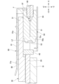
- the biasing portion 82a is formed on the first side plate 82 and biases the pressure receiving surface 53 of the ferrule 50 toward the +Y side. As shown in FIG. 5, when the ferrule 50 is biased by the biasing portion 82a, the sliding surface 54 comes into contact with the receptacle-side sliding surface 34. Thereby, the relative positions of the ferrule 50 and the receptacle 30 in the first direction Y are determined.
- the receptacle-side sliding surface 34 and the sliding surface 54 are portions that serve as a position reference in the first direction Y.
- the two second biasing parts 81a are formed on the upper plate 81.
- the number of second biasing parts 81a may be one.
- the second biasing portion 81a presses the upper wall 31 of the receptacle 30 toward the ⁇ Z side.
- the first support plate 84 and the second support plate 85 are in contact with the lower surface (-Z side end surface) of the ferrule 50 and support the ferrule 50 from the -Z side. That is, the upper wall 31 of the receptacle 30 and the ferrule 50 are sandwiched in the second direction Z between the first support plate 84, the second support plate 85, and the second biasing portion 81a.
- the lower surface of the upper wall 31 (the end surface on the ⁇ Z side) and the upper surface of the ferrule 50 (the end surface on the +Z side) are portions that serve as a position reference in the second direction Z.
- the third biasing portion 87 protrudes from the -X side end of the upper plate 81 toward the -Z side.
- the third biasing portion 87 biases the ferrule 50 toward the +X side.
- the longitudinal reference surface 50a comes into contact with the positioning surface 35.
- the longitudinal reference surface 50a and the positioning surface 35 are reference surfaces that determine the position of the ferrule 50 with respect to the receptacle 30 in the longitudinal direction X.
- a reaction force directed toward the ⁇ X side due to the urging force of the third urging portion 87 acts on the holding member 80. This reaction force is supported by the protrusion 31a of the receptacle 30 via the locking portion 86.
- positioning is performed by abutting the ferrule 50 and the receptacle 30 in three directions (X, Y, Z) without using a positioning pin.
- a positioning pin it is possible to reduce the external dimensions of the ferrule 50 (particularly the dimensions in the first direction Y). Therefore, more optical connection units U can be arranged on the board 10, and the arrangement density of optical fibers F in a data center or the like can be increased.
- FIG. 5 shows a center line O passing through the center of the ferrule 50 in the longitudinal direction X.
- the longitudinal reference surface 50a is located between this center line O and the lens forming surface 52 in the longitudinal direction X.
- This arrangement provides the following effects. If the longitudinal reference surface 50a is placed at the tip (+X side end) of the ferrule 50, the distance between the longitudinal reference surface 50a and the lens forming surface 52 will become too short. Therefore, when the longitudinal reference surface 50a abuts against the positioning surface 35, dust and the like tend to adhere to the lens L2. If dust or the like adheres to the lens L2, it will lead to an increase in optical connection loss between the optical integrated circuit 20 and the optical fiber F.
- the longitudinal reference surface 50a is placed at the base end (-X side end) of the ferrule 50, the distance between the longitudinal reference surface 50a and the lens L2 will be too long. Therefore, when the ferrule 50 is held with the longitudinal reference plane 50a tilted with respect to the positioning plane 35, the positional deviation of the lens L2 with respect to the lens L1 increases. In this case as well, the optical connection loss between the optical integrated circuit 20 and the optical fiber F increases.
- the longitudinal reference plane 50a between the center line O and the lens forming surface 52 as in the present embodiment, the attachment of dust to the lens L2 can be suppressed while Positional deviation with respect to L1 can also be suppressed. Therefore, when positioning the ferrule 50 without using pins, the quality of the optical connection can be stabilized.
- FIGS. 7A, 7B, and 7C the effects obtained by providing the recess 34a and the inclined surface 34b will be described using FIGS. 7A, 7B, and 7C.
- the ferrule 50 is pushed toward the +X side while sliding the sliding surface 54 of the ferrule 50 onto the receptacle-side sliding surface 34.
- the recess 34a it has been found that if the recess 34a is not provided, the connection between the optical connector C and the receptacle 30 is easily completed with the sliding surface 54 tilted with respect to the receptacle-side sliding surface 34. Ta.
- a biasing force is applied to the ferrule 50 by the biasing portion 82a, and once the sliding surface 54 is tilted with respect to the receptacle-side sliding surface 34, the biasing force is applied to maintain the tilted state. There is a possibility that it will happen.
- the biasing force directed toward the +Y side by the biasing portion 82a acts near the center of gravity of the ferrule 50, the ferrule 50 is less likely to tilt. Furthermore, the position of the contact point in the longitudinal direction X coincides with the position of the recess 34a. Therefore, the biasing force by the biasing portion 82a acts to press the sliding surface 54 in a well-balanced manner against the receptacle-side sliding surface 34 which is divided into two parts. Thereby, tilting of the ferrule 50 with respect to the receptacle 30 can be effectively suppressed.
- this embodiment provides the ferrule 50 that is connected to the receptacle 30 fixed to the optical integrated circuit 20.
- the ferrule 50 has a fiber hole 51 into which the optical fiber F is inserted, a light exit surface (the surface of the lens L2 in this embodiment) through which the light passing through the optical fiber F is emitted, and a longitudinal direction of the ferrule 50 with respect to the receptacle 30. It has a longitudinal reference surface 50a that determines the position in X.
- the longitudinal reference surface 50a is located between the center line O passing through the center position of the ferrule 50 in the longitudinal direction X and the light exit surface.
- the ferrule 50 has a lens L2 arranged at a position overlapping the fiber hole 51 when viewed from the longitudinal direction X.
- the light exit surface is the surface of the lens L2.
- the dimension between the longitudinal reference surface 50a and the light exit surface in the longitudinal direction X varies, the optical characteristics of the ferrule 50 will be affected. Therefore, the dimension between the longitudinal reference surface 50a and the light exit surface in the longitudinal direction X is required to have small manufacturing variations.
- the smaller the dimension between the longitudinal reference surface 50a and the light emitting surface that is, the closer the longitudinal reference surface 50a and the light emitting surface are in the longitudinal direction X), the easier it is to suppress manufacturing variations.
- the longitudinal reference plane 50a is located between the light exit surface (the surface of the lens L2) and the abutting surface 51a.
- the distance between the abutting surface 51a and the light exit surface is set small so that the optical signal emitted from the tip of the optical fiber F is not dispersed within the ferrule 50. Therefore, by positioning the longitudinal reference surface 50a between the light emitting surface and the abutment surface 51a, the dimension between the longitudinal reference surface 50a and the light emitting surface can be reduced, and the above-described manufacturing variations can be reduced.
- the ferrule 50 has a dustproof wall 56 that protrudes from the longitudinal reference surface 50a and surrounds the light exit surface.
- the dustproof wall 56 can more effectively suppress dust and the like from adhering to the light exit surface.
- the tip of the dustproof wall 56 the end surface on the + etc. may enter the inside of the dustproof wall 56 and adhere to the light exit surface.
- the dustproof wall 56 protrudes from the longitudinal reference surface 50a, it becomes more difficult for shavings and the like to adhere to the light emitting surface.
- the optical connection structure 1 of this embodiment includes a ferrule 50, a receptacle 30, and a holding member 80 that holds the ferrule 50 and the receptacle 30 in a positioned state.
- the ferrule 50 has a pressure receiving surface 53 that receives an urging force in a direction intersecting the longitudinal direction X of the fiber hole 51 (first direction Y in this embodiment), and is disposed apart from the pressure receiving surface 53 and slides with the receptacle 30. It has a sliding surface 54.
- the holding member 80 has a biasing portion 82a that applies a biasing force to the pressure receiving surface 53, and the receptacle 30 has a receptacle-side sliding surface 34 that slides on the sliding surface 54.
- a recess 34a into which a part of the ferrule 50 can enter is formed in the receptacle side sliding surface 34.
- An inclined surface 34b is formed.
- the receptacle side sliding surface 34 is divided into two parts in the longitudinal direction X by the recess 34a.
- the sliding surface 54 of the ferrule 50 is pressed against the receptacle-side sliding surface 34 divided into two parts, so that the tilting of the ferrule 50 can be suppressed more reliably.
- the light exit surface of the ferrule 50 may not be the surface of the lens L2.
- the surface 52 may be used as the light exit surface.
- Optical connection structure 20 Optical integrated circuit 30
- Receptacle 34 Receptacle side sliding surface 34a
- Concavity 34b ... Inclined surface 50
- Ferrule 50a Longitudinal reference surface 51
- Fiber hole 51a Abutment surface 53
- Pressure receiving surface 54 Sliding Moving surface 56
- dust-proof wall 80 ...holding member 82a...biasing part F...optical fiber
Abstract
A purpose of the present invention is to provide an optical connection structure and a ferrule capable of stabilizing optical connection quality when performing positioning without using pins. A ferrule (50) according to the present invention comprises: a fiber pore (51) into which an optical fiber (F) is to be inserted; a light emission face from which light having passed through the optical fiber (F) is to be emitted; and a longitudinal reference face (50a) which positions the ferrule (50) in the longitudinal direction with respect to a receptacle (30). The longitudinal reference face (50a) is located between the center line (O) passing through the center position of the ferrule (50) in the longitudinal direction and the light emission face.
Description
本発明は、フェルールおよび光接続構造に関する。
本願は、2022年3月9日に日本に出願された特願2022-036444号について優先権を主張し、その内容をここに援用する。 The present invention relates to a ferrule and an optical connection structure.
This application claims priority to Japanese Patent Application No. 2022-036444 filed in Japan on March 9, 2022, the contents of which are incorporated herein.
特許文献1には、光学素子(photonic element)と光ファイバとを接続するための光接続構造が開示されている。特許文献1において、光ファイバの長手方向に直交する方向における光コネクタの位置決めは、位置決め用のピンによって行われる。また、長手方向における光コネクタの位置決めは、光コネクタのフェルールをアダプタに対して突き当てることで行われる。
Patent Document 1 discloses an optical connection structure for connecting an optical element and an optical fiber. In Patent Document 1, positioning of the optical connector in a direction perpendicular to the longitudinal direction of the optical fiber is performed using positioning pins. Further, the positioning of the optical connector in the longitudinal direction is performed by abutting the ferrule of the optical connector against the adapter.
特許文献1においては、ピンの太さの分だけ、フェルールの外形寸法が大きくなっている。ピンを用いず、フェルールの外形を用いて位置決めを行えば、フェルールの小型化を図ることができる。
ここで、本願発明者らが検討したところ、ピンを用いずにフェルールの位置決めを行う場合、長手方向におけるフェルール位置の基準となる基準面の配置が、光コネクタを用いた光接続の品質に影響を及ぼすことが判った。 InPatent Document 1, the outer dimensions of the ferrule are increased by the thickness of the pin. If positioning is performed using the outer shape of the ferrule without using pins, the ferrule can be made smaller.
Here, the inventors of the present invention have investigated that when positioning the ferrule without using pins, the arrangement of the reference plane that serves as a reference for the ferrule position in the longitudinal direction affects the quality of the optical connection using the optical connector. It was found that
ここで、本願発明者らが検討したところ、ピンを用いずにフェルールの位置決めを行う場合、長手方向におけるフェルール位置の基準となる基準面の配置が、光コネクタを用いた光接続の品質に影響を及ぼすことが判った。 In
Here, the inventors of the present invention have investigated that when positioning the ferrule without using pins, the arrangement of the reference plane that serves as a reference for the ferrule position in the longitudinal direction affects the quality of the optical connection using the optical connector. It was found that
本発明はこのような事情を考慮してなされ、ピンを用いずに位置決めを行うにあたり、光接続の品質を安定させることが可能なフェルールおよび光接続構造を提供することを目的とする。
The present invention was made in consideration of these circumstances, and an object of the present invention is to provide a ferrule and an optical connection structure that can stabilize the quality of optical connections when positioning is performed without using pins.
上記課題を解決するために、本発明の一態様に係るフェルールは、光集積回路に固定されたレセプタクルに接続されるフェルールであって、光ファイバが挿入されるファイバ孔と、前記光ファイバを通った光が出射される光出射面と、前記光ファイバの長手方向における、前記フェルールの前記レセプタクルに対する位置を決める長手基準面と、を有し、前記長手基準面は、前記長手方向における前記フェルールの中心位置を通る中心線と、前記光出射面と、の間に位置している。
In order to solve the above problems, a ferrule according to one aspect of the present invention is a ferrule that is connected to a receptacle fixed to an optical integrated circuit, and includes a fiber hole into which an optical fiber is inserted, and a fiber hole through which the optical fiber is inserted. and a longitudinal reference surface that determines the position of the ferrule with respect to the receptacle in the longitudinal direction of the optical fiber, and the longitudinal reference surface determines the position of the ferrule in the longitudinal direction of the optical fiber. It is located between the center line passing through the center position and the light exit surface.
また、本発明の一態様に係る光接続構造は、前記フェルールと、前記レセプタクルと、前記フェルールと前記レセプタクルとが位置決めされた状態を保持する保持部材と、を備え、前記フェルールは、前記長手方向に交差する方向の付勢力を受ける受圧面と、前記受圧面から離れて配置されて前記レセプタクルと摺動する摺動面と、を有し、前記保持部材は、前記受圧面に前記付勢力を加える付勢部を有し、前記レセプタクルは、前記摺動面と摺動するレセプタクル側摺動面を有し、前記レセプタクル側摺動面には、前記フェルールの一部が進入可能な凹部が形成され、前記長手方向において前記光出射面から光が出射される向きを前方とするとき、前記凹部の内側に、前方に向かうに従って前記レセプタクル側摺動面に近づくように傾斜する傾斜面が形成されている。
Further, the optical connection structure according to one aspect of the present invention includes the ferrule, the receptacle, and a holding member that holds the ferrule and the receptacle in a positioned state, and the ferrule is arranged in the longitudinal direction. the holding member has a pressure-receiving surface that receives a biasing force in a direction intersecting with the pressure-receiving surface, and a sliding surface that is arranged apart from the pressure-receiving surface and slides on the receptacle, and the holding member applies the biasing force to the pressure-receiving surface. the receptacle has a receptacle-side sliding surface that slides on the sliding surface, and the receptacle-side sliding surface has a recess into which a portion of the ferrule can enter. and when the direction in which light is emitted from the light emitting surface in the longitudinal direction is the forward direction, an inclined surface is formed inside the recessed portion such that the inclined surface approaches the receptacle side sliding surface toward the front. ing.
本発明の上記態様によれば、ピンを用いずに位置決めを行うにあたり、光接続の品質を安定させることが可能なフェルールおよび光接続構造を提供することができる。
According to the above aspects of the present invention, it is possible to provide a ferrule and an optical connection structure that can stabilize the quality of optical connections when positioning is performed without using pins.
以下、本実施形態のフェルールおよび光接続構造について図面に基づいて説明する。
図1に示すように、光接続構造1は、基板10と、複数の光接続ユニットUと、を備える。図2、図3A、図3Bに示すように、各光接続ユニットUは、光集積回路20と、レセプタクル30と、マイクロレンズアレイ40と、光コネクタCと、保持部材80と、を備える。光コネクタCは、フェルール50と、ブーツ60と、テープ心線70と、を備える。フェルール50には、複数の光ファイバFを挿入可能な複数のファイバ孔51(図4、図6参照)が形成されている。複数のファイバ孔51は、各ファイバ孔51の長手方向と直交する一方向に沿って配列されている。 The ferrule and optical connection structure of this embodiment will be described below based on the drawings.
As shown in FIG. 1, theoptical connection structure 1 includes a substrate 10 and a plurality of optical connection units U. As shown in FIGS. 2, 3A, and 3B, each optical connection unit U includes an optical integrated circuit 20, a receptacle 30, a microlens array 40, an optical connector C, and a holding member 80. The optical connector C includes a ferrule 50, a boot 60, and a tape core wire 70. The ferrule 50 is formed with a plurality of fiber holes 51 (see FIGS. 4 and 6) into which a plurality of optical fibers F can be inserted. The plurality of fiber holes 51 are arranged along one direction orthogonal to the longitudinal direction of each fiber hole 51.
図1に示すように、光接続構造1は、基板10と、複数の光接続ユニットUと、を備える。図2、図3A、図3Bに示すように、各光接続ユニットUは、光集積回路20と、レセプタクル30と、マイクロレンズアレイ40と、光コネクタCと、保持部材80と、を備える。光コネクタCは、フェルール50と、ブーツ60と、テープ心線70と、を備える。フェルール50には、複数の光ファイバFを挿入可能な複数のファイバ孔51(図4、図6参照)が形成されている。複数のファイバ孔51は、各ファイバ孔51の長手方向と直交する一方向に沿って配列されている。 The ferrule and optical connection structure of this embodiment will be described below based on the drawings.
As shown in FIG. 1, the
(方向定義)
ここで、本実施形態では、XYZ直交座標系を設定して各構成の位置関係を説明する。X軸方向は、各ファイバ孔51の長手方向に沿う方向である。Y軸方向は、複数のファイバ孔51が配列される方向である。Z軸方向は、X軸およびY軸の双方に直交する方向である。本明細書では、X軸方向を長手方向Xと称し、Y軸方向を第1方向Yと称し、Z軸方向を第2方向Zと称する場合がある。長手方向Xに沿って、フェルール50から光集積回路20に向かう方向を、+X側または前方と称する。+X側とは反対の方向を、-X側または後方と称する。第1方向Yに沿う一方向を、+Y側または左方と称する。+Y側とは反対の方向を、-Y側または右方と称する。第2方向Zに沿って、基板10から光集積回路20に向かう方向を、+Z側または上方と称する。+Z側とは反対の方向を、-Z側または下方と称する。 (direction definition)
Here, in this embodiment, an XYZ orthogonal coordinate system is set to explain the positional relationship of each component. The X-axis direction is a direction along the longitudinal direction of eachfiber hole 51. The Y-axis direction is the direction in which the plurality of fiber holes 51 are arranged. The Z-axis direction is a direction perpendicular to both the X-axis and the Y-axis. In this specification, the X-axis direction is sometimes referred to as the longitudinal direction X, the Y-axis direction is sometimes referred to as the first direction Y, and the Z-axis direction is sometimes referred to as the second direction Z. The direction from the ferrule 50 toward the optical integrated circuit 20 along the longitudinal direction X is referred to as the +X side or the front. The direction opposite to the +X side is referred to as the -X side or rearward. One direction along the first direction Y is referred to as the +Y side or the left side. The direction opposite to the +Y side is called the -Y side or right side. The direction from the substrate 10 toward the optical integrated circuit 20 along the second direction Z is referred to as the +Z side or upward. The direction opposite to the +Z side is referred to as the -Z side or downward direction.
ここで、本実施形態では、XYZ直交座標系を設定して各構成の位置関係を説明する。X軸方向は、各ファイバ孔51の長手方向に沿う方向である。Y軸方向は、複数のファイバ孔51が配列される方向である。Z軸方向は、X軸およびY軸の双方に直交する方向である。本明細書では、X軸方向を長手方向Xと称し、Y軸方向を第1方向Yと称し、Z軸方向を第2方向Zと称する場合がある。長手方向Xに沿って、フェルール50から光集積回路20に向かう方向を、+X側または前方と称する。+X側とは反対の方向を、-X側または後方と称する。第1方向Yに沿う一方向を、+Y側または左方と称する。+Y側とは反対の方向を、-Y側または右方と称する。第2方向Zに沿って、基板10から光集積回路20に向かう方向を、+Z側または上方と称する。+Z側とは反対の方向を、-Z側または下方と称する。 (direction definition)
Here, in this embodiment, an XYZ orthogonal coordinate system is set to explain the positional relationship of each component. The X-axis direction is a direction along the longitudinal direction of each
本実施形態では、複数の光ファイバFがまとめて被覆される、または互いが間欠的に固定されることでテープ心線70が構成されている。なお、複数の光ファイバFがテープ心線70を構成せず、各光ファイバFが個別に被覆されていてもよい。ブーツ60は長手方向Xに延びる筒状であり、テープ心線70はブーツ60内に挿通されている。ブーツ60は、弾性を有する材質によって形成され、フェルール50から-X側に向けて延出している。ブーツ60は、光ファイバFに加わる曲げおよび応力を緩和する役割を有する。
In the present embodiment, the tape core wire 70 is configured by covering a plurality of optical fibers F together or by intermittently fixing each other. Note that the plurality of optical fibers F may not constitute the ribbon cable 70, and each optical fiber F may be individually coated. The boot 60 has a cylindrical shape extending in the longitudinal direction X, and the tape core wire 70 is inserted into the boot 60. The boot 60 is made of an elastic material and extends from the ferrule 50 toward the −X side. The boot 60 has the role of alleviating bending and stress applied to the optical fiber F.
図1に示すように、基板10の上面には電子部品11が実装されている。また、基板10には、電子部品11に電気的に接続された回路パターン(不図示)が形成されている。電子部品11は、例えば、スイッチ回路等であってもよい。複数の光接続ユニットUは、電子部品11を取り囲むように配置されている。
As shown in FIG. 1, electronic components 11 are mounted on the upper surface of the board 10. Furthermore, a circuit pattern (not shown) electrically connected to the electronic component 11 is formed on the substrate 10. The electronic component 11 may be, for example, a switch circuit. The plurality of optical connection units U are arranged so as to surround the electronic component 11.
光集積回路20は、基板10の上面に実装されている。光集積回路20は、直方体状に形成されている。光集積回路20は、光信号を電気信号に変換する不図示の受光素子と、電気信号を光信号に変換する不図示の発光素子と、を有する。受光素子としては、例えばフォトダイオード等のフォトディテクターを用いることができる。発光素子としては、例えば半導体レーザや発光ダイオード等を用いることができる。
The optical integrated circuit 20 is mounted on the upper surface of the substrate 10. The optical integrated circuit 20 is formed into a rectangular parallelepiped shape. The optical integrated circuit 20 includes a light receiving element (not shown) that converts an optical signal into an electrical signal, and a light emitting element (not shown) that converts the electrical signal into an optical signal. As the light receiving element, for example, a photodetector such as a photodiode can be used. As the light emitting element, for example, a semiconductor laser, a light emitting diode, etc. can be used.
図3Bにおいて、光集積回路20、マイクロレンズアレイ40、およびレセプタクル30は、接着剤によって互いに固定されている。例えば、マイクロレンズアレイ40の前面(+X側の端面)が、光集積回路20の後面(-X側の端面)に接着固定されてもよい。この場合、光信号は接着剤の層を通過するため、接着剤は光を透過する材質であることが好ましい。ただし、光集積回路20、レセプタクル30、およびマイクロレンズアレイ40の固定方法は上記に限定されず、適宜変更してもよい。
In FIG. 3B, the optical integrated circuit 20, the microlens array 40, and the receptacle 30 are fixed to each other with an adhesive. For example, the front surface (+X side end surface) of the microlens array 40 may be adhesively fixed to the rear surface (−X side end surface) of the optical integrated circuit 20. In this case, since the optical signal passes through the adhesive layer, the adhesive is preferably a material that transmits light. However, the method of fixing the optical integrated circuit 20, the receptacle 30, and the microlens array 40 is not limited to the above, and may be changed as appropriate.
図4に示すように、光集積回路20は、複数の導波路21を有する。なお、図4以外の図において、導波路21の図示は省略されている。各導波路21は、上述した受光素子および発光素子と光学的に接続されている。本実施形態において、各導波路21は、長手方向Xに沿って延びている。各導波路21は、例えばシリコンによって形成されている。導波路21の屈折率は、光集積回路20のうち導波路21以外の部分の屈折率よりも、高い。これにより、光信号が導波路21の内部に閉じ込められ、光信号は長手方向Xに伝搬する。導波路21は、光集積回路20の表面(上面)に設けられていてもよいし、光集積回路20の内部に設けられていてもよい。各導波路21の後端(-X側の端部)には、入射出部21aが設けられている。入射出部21aは、導波路21の一部分であり、光信号の受け取りおよび放出を行う。
As shown in FIG. 4, the optical integrated circuit 20 has a plurality of waveguides 21. Note that in figures other than FIG. 4, illustration of the waveguide 21 is omitted. Each waveguide 21 is optically connected to the above-mentioned light receiving element and light emitting element. In this embodiment, each waveguide 21 extends along the longitudinal direction X. Each waveguide 21 is made of silicon, for example. The refractive index of the waveguide 21 is higher than the refractive index of a portion of the optical integrated circuit 20 other than the waveguide 21 . Thereby, the optical signal is confined inside the waveguide 21, and the optical signal propagates in the longitudinal direction X. The waveguide 21 may be provided on the surface (upper surface) of the optical integrated circuit 20 or may be provided inside the optical integrated circuit 20. At the rear end (-X side end) of each waveguide 21, an input/output section 21a is provided. The input/output section 21a is a part of the waveguide 21, and receives and emits optical signals.
図4に示すように、フェルール50が有するファイバ孔51の内側には、光ファイバFの+X側の端部が突き当てられる突当面51aが形成されている。突当面51aは-X側を向いている。光コネクタCが組み立てられる際、複数の光ファイバFはそれぞれ複数のファイバ孔51に挿入され、ファイバ孔51の各突当面51aに突き当てられる。
フェルール50は、長手方向Xにおいてマイクロレンズアレイ40と対向するレンズ形成面52を有している。レンズ形成面52には、第1方向Yにおいて並べられた複数のレンズL2が形成されている。 As shown in FIG. 4, anabutment surface 51a against which the +X side end of the optical fiber F abuts is formed inside the fiber hole 51 of the ferrule 50. The abutment surface 51a faces the −X side. When the optical connector C is assembled, the plurality of optical fibers F are respectively inserted into the plurality of fiber holes 51 and abutted against the respective abutting surfaces 51a of the fiber holes 51.
Theferrule 50 has a lens forming surface 52 that faces the microlens array 40 in the longitudinal direction X. A plurality of lenses L2 arranged in the first direction Y are formed on the lens forming surface 52.
フェルール50は、長手方向Xにおいてマイクロレンズアレイ40と対向するレンズ形成面52を有している。レンズ形成面52には、第1方向Yにおいて並べられた複数のレンズL2が形成されている。 As shown in FIG. 4, an
The
マイクロレンズアレイ40は、光を透過できる部材で形成されている。マイクロレンズアレイ40は、例えば、石英ガラスやシリコン基板によって形成されていてもよい。本実施形態において、マイクロレンズアレイ40の形状は、矩形の板状である。図3Bに示すように、マイクロレンズアレイ40には、複数のレンズL1が形成されている。
The microlens array 40 is made of a material that can transmit light. The microlens array 40 may be formed of, for example, quartz glass or a silicon substrate. In this embodiment, the shape of the microlens array 40 is a rectangular plate. As shown in FIG. 3B, a plurality of lenses L1 are formed in the microlens array 40.
光コネクタCがレセプタクル30に接続されると、図4に示すように、フェルール50とマイクロレンズアレイ40とが長手方向Xにおいて対向する。より詳しくは、フェルール50に形成された複数のレンズL2が、マイクロレンズアレイ40の複数のレンズL1に対して対向する。光ファイバF内を+X側に進行した光信号は、ファイバ孔51の突当面51aからフェルール50内に進入する。また、光信号は、フェルール50のレンズL2から+X側に出射する。つまり、レンズL2の表面は、フェルール50から光が出射される光出射面である。
When the optical connector C is connected to the receptacle 30, the ferrule 50 and the microlens array 40 face each other in the longitudinal direction X, as shown in FIG. More specifically, the plurality of lenses L2 formed on the ferrule 50 face the plurality of lenses L1 of the microlens array 40. The optical signal that has traveled within the optical fiber F toward the +X side enters the ferrule 50 from the abutment surface 51a of the fiber hole 51. Further, the optical signal is emitted from the lens L2 of the ferrule 50 to the +X side. That is, the surface of the lens L2 is a light exit surface from which light is emitted from the ferrule 50.
フェルール50から出射された光は、レンズL1からマイクロレンズアレイ40内に入射する。また、マイクロレンズアレイ40内を通った光は、光集積回路20の入射出部21aによって受け取られ、導波路21中を伝播する。そして、光信号は、光集積回路20が備える受光素子によって電気信号に変換され、基板10に受け渡される。逆に、基板10から光集積回路20へと伝わってきた電気信号は、光集積回路20が備える発光素子によって光信号に変換される。そして、この光信号は、導波路21中を伝播し、入射出部21aから光ファイバFに向けて放出される。このようにして、光接続構造1は、光ファイバFと光集積回路20との間で光の接続を行う。
The light emitted from the ferrule 50 enters the microlens array 40 through the lens L1. Further, the light passing through the microlens array 40 is received by the input/output section 21 a of the optical integrated circuit 20 and propagates through the waveguide 21 . The optical signal is then converted into an electrical signal by a light receiving element included in the optical integrated circuit 20 and delivered to the substrate 10. Conversely, an electrical signal transmitted from the substrate 10 to the optical integrated circuit 20 is converted into an optical signal by a light emitting element included in the optical integrated circuit 20. Then, this optical signal propagates through the waveguide 21 and is emitted toward the optical fiber F from the input/output section 21a. In this way, the optical connection structure 1 performs optical connection between the optical fiber F and the optical integrated circuit 20.
光コネクタCは、レセプタクル30に取り付けられ、また、レセプタクル30から取り外すことができる(詳細は後述)。レセプタクル30は、光コネクタCのフェルール50を光集積回路20に対して位置決めする役割を有する。
図3Bに示すように、レセプタクル30は、上壁31と、第1側壁32と、第2側壁33と、を有する。上壁31は、第1方向Yおよび長手方向Xに延在する板状である。第1側壁32は、上壁31の+Y側の端部から、-Z側に向けて延びている。第2側壁33は、上壁31の-Y側の端部から、-Z側に向けて延びている。長手方向Xにおける寸法を比較すると、第2側壁33の寸法は第1側壁32の寸法よりも短い。第1側壁32と第2側壁33とは第1方向Yにおいて間隔を空けて配置されている。光コネクタCがレセプタクル30に接続される際、第1側壁32と第2側壁33との間にフェルール50が進入する。 The optical connector C is attached to thereceptacle 30 and can be removed from the receptacle 30 (details will be described later). The receptacle 30 has the role of positioning the ferrule 50 of the optical connector C with respect to the optical integrated circuit 20.
As shown in FIG. 3B, thereceptacle 30 has a top wall 31, a first side wall 32, and a second side wall 33. The upper wall 31 has a plate shape extending in the first direction Y and the longitudinal direction X. The first side wall 32 extends from the +Y side end of the upper wall 31 toward the -Z side. The second side wall 33 extends from the -Y side end of the upper wall 31 toward the -Z side. Comparing the dimensions in the longitudinal direction X, the dimension of the second side wall 33 is shorter than the dimension of the first side wall 32. The first side wall 32 and the second side wall 33 are spaced apart in the first direction Y. When the optical connector C is connected to the receptacle 30, the ferrule 50 enters between the first side wall 32 and the second side wall 33.
図3Bに示すように、レセプタクル30は、上壁31と、第1側壁32と、第2側壁33と、を有する。上壁31は、第1方向Yおよび長手方向Xに延在する板状である。第1側壁32は、上壁31の+Y側の端部から、-Z側に向けて延びている。第2側壁33は、上壁31の-Y側の端部から、-Z側に向けて延びている。長手方向Xにおける寸法を比較すると、第2側壁33の寸法は第1側壁32の寸法よりも短い。第1側壁32と第2側壁33とは第1方向Yにおいて間隔を空けて配置されている。光コネクタCがレセプタクル30に接続される際、第1側壁32と第2側壁33との間にフェルール50が進入する。 The optical connector C is attached to the
As shown in FIG. 3B, the
図3Aに示すように、上壁31には、+Z側に向けて突出する突起31aが形成されている。突起31aには、保持部材80の係止部86(後述)が係止される。
図3Bに示すように、第1側壁32は、-Y側を向くレセプタクル側摺動面34を有する。レセプタクル側摺動面34には、+Y側に向けて窪む凹部34aが形成されている。レセプタクル側摺動面34は、凹部34aによって、長手方向Xにおいて離れた2つの部位に分断されている。
図5に示すように、凹部34aの内側には、傾斜面34bが形成されている。傾斜面34bは、+X側に向かうに従って-Y側に向かうように傾斜している。言い換えると、傾斜面34bは、+X側に向かうに従ってレセプタクル側摺動面34に近づくように傾斜している。 As shown in FIG. 3A, theupper wall 31 is formed with a protrusion 31a that protrudes toward the +Z side. A locking portion 86 (described later) of the holding member 80 is locked to the protrusion 31a.
As shown in FIG. 3B, thefirst side wall 32 has a receptacle-side sliding surface 34 facing the −Y side. A recess 34a is formed in the receptacle side sliding surface 34 and is recessed toward the +Y side. The receptacle side sliding surface 34 is divided into two parts separated in the longitudinal direction X by the recess 34a.
As shown in FIG. 5, aninclined surface 34b is formed inside the recess 34a. The inclined surface 34b is inclined toward the −Y side as it goes toward the +X side. In other words, the inclined surface 34b is inclined so as to approach the receptacle-side sliding surface 34 as it goes toward the +X side.
図3Bに示すように、第1側壁32は、-Y側を向くレセプタクル側摺動面34を有する。レセプタクル側摺動面34には、+Y側に向けて窪む凹部34aが形成されている。レセプタクル側摺動面34は、凹部34aによって、長手方向Xにおいて離れた2つの部位に分断されている。
図5に示すように、凹部34aの内側には、傾斜面34bが形成されている。傾斜面34bは、+X側に向かうに従って-Y側に向かうように傾斜している。言い換えると、傾斜面34bは、+X側に向かうに従ってレセプタクル側摺動面34に近づくように傾斜している。 As shown in FIG. 3A, the
As shown in FIG. 3B, the
As shown in FIG. 5, an
第1側壁32には、-X側を向く位置決め面35が形成されている。位置決め面35は、レセプタクル側摺動面34よりも+X側に位置している。位置決め面35は、長手方向Xにおけるレセプタクル30とフェルール50との相対位置を決める役割を有する。なお、第2側壁33にも、第1側壁32の位置決め面35と同一平面内に位置する位置決め面が形成されている。これら2つの位置決め面に、フェルール50が突き当てられる。
A positioning surface 35 facing the -X side is formed on the first side wall 32. The positioning surface 35 is located on the +X side with respect to the receptacle side sliding surface 34. The positioning surface 35 has a role of determining the relative position of the receptacle 30 and the ferrule 50 in the longitudinal direction X. Note that the second side wall 33 is also formed with a positioning surface located in the same plane as the positioning surface 35 of the first side wall 32 . The ferrule 50 is abutted against these two positioning surfaces.
図3Cに示すように、フェルール50は略直方体状に形成されている。フェルール50は、例えば透過性を有する樹脂を材質とする成型品である。フェルール50は、長手基準面50aと、複数のファイバ孔51(図4参照)と、レンズ形成面52と、受圧面53と、摺動面54と、充填孔55と、防塵壁56と、を有する。複数のファイバ孔51は、第1方向Yに並んでいる。レンズ形成面52には、+X側に突出するように、複数のレンズL2が形成されている。レンズ形成面52は、防塵壁56およびレンズL2を除けば、フェルール50において最も+X側に位置する面である。
As shown in FIG. 3C, the ferrule 50 is formed into a substantially rectangular parallelepiped shape. The ferrule 50 is a molded product made of, for example, a transparent resin. The ferrule 50 includes a longitudinal reference surface 50a, a plurality of fiber holes 51 (see FIG. 4), a lens forming surface 52, a pressure receiving surface 53, a sliding surface 54, a filling hole 55, and a dustproof wall 56. have The plurality of fiber holes 51 are lined up in the first direction Y. A plurality of lenses L2 are formed on the lens forming surface 52 so as to protrude toward the +X side. The lens forming surface 52 is the surface located on the +X side of the ferrule 50, excluding the dustproof wall 56 and the lens L2.
各レンズL2の位置は、各ファイバ孔51の位置に対応している。より具体的には、長手方向Xから見たとき、各レンズL2は各ファイバ孔51と重なる位置に配置されている。防塵壁56は、長手基準面50aから+X側に突出している。防塵壁56は長手方向Xから見て矩形の枠状であり、レンズ形成面52およびレンズL2を囲っている。防塵壁56は、レンズ形成面52およびレンズL2に塵等が付着することを防止する役割を有する。ただし、防塵壁56は無くてもよい。
The position of each lens L2 corresponds to the position of each fiber hole 51. More specifically, when viewed from the longitudinal direction X, each lens L2 is arranged at a position overlapping each fiber hole 51. The dustproof wall 56 protrudes from the longitudinal reference surface 50a toward the +X side. The dustproof wall 56 has a rectangular frame shape when viewed from the longitudinal direction X, and surrounds the lens forming surface 52 and the lens L2. The dustproof wall 56 has a role of preventing dust and the like from adhering to the lens forming surface 52 and the lens L2. However, the dustproof wall 56 may not be provided.
充填孔55はフェルール50を第2方向Zにおいて貫通している。光コネクタCを組み立てる際、光ファイバFがファイバ孔51内に挿入された後で、充填孔55から接着剤が注入される。これにより、光ファイバFをフェルール50に固定することができる。
The filling hole 55 penetrates the ferrule 50 in the second direction Z. When assembling the optical connector C, after the optical fiber F is inserted into the fiber hole 51, adhesive is injected through the filling hole 55. Thereby, the optical fiber F can be fixed to the ferrule 50.
受圧面53および摺動面54は、第1方向Yにおけるフェルール50の両端面である。本実施形態では、受圧面53が-Y側の端面であり、摺動面54が+Y側の端面である。ただし、受圧面53と摺動面54との位置関係は逆であってもよい。受圧面53は、保持部材80の付勢部82a(後述)から付勢力を受ける部位である。摺動面54は、レセプタクル30と摺動する部位である。すなわち、光コネクタCがレセプタクル30に接続される際に、フェルール50は、摺動面54においてレセプタクル30と摺動する。
The pressure receiving surface 53 and the sliding surface 54 are both end surfaces of the ferrule 50 in the first direction Y. In this embodiment, the pressure receiving surface 53 is the end surface on the -Y side, and the sliding surface 54 is the end surface on the +Y side. However, the positional relationship between the pressure receiving surface 53 and the sliding surface 54 may be reversed. The pressure receiving surface 53 is a portion that receives a biasing force from a biasing portion 82a (described later) of the holding member 80. The sliding surface 54 is a part that slides on the receptacle 30. That is, when the optical connector C is connected to the receptacle 30, the ferrule 50 slides on the receptacle 30 on the sliding surface 54.
保持部材80は、フェルール50がレセプタクル30に位置決めされた状態を保持する役割を有する。図3Aに示すように、保持部材80は、上板81と、第1側板82と、第2側板83と、第1支持板84と、第2支持板85と、係止部86と、を有する。本実施形態の保持部材80は金属の板を型加工することで形成されている。ただし、保持部材80の材質、形状、製法は適宜変更してもよい。
The holding member 80 has the role of maintaining the ferrule 50 positioned in the receptacle 30. As shown in FIG. 3A, the holding member 80 includes an upper plate 81, a first side plate 82, a second side plate 83, a first support plate 84, a second support plate 85, and a locking portion 86. have The holding member 80 of this embodiment is formed by molding a metal plate. However, the material, shape, and manufacturing method of the holding member 80 may be changed as appropriate.
図2に示すように、保持部材80が光コネクタCおよびレセプタクル30の相対位置を保持する状態において、上板81はレセプタクル30の+Z側に位置し、第1支持板84および第2支持板85はレセプタクル30の-Z側に位置する。また、第1側板82と第2側板83との間にレセプタクル30およびフェルール50が配置される。
As shown in FIG. 2, when the holding member 80 holds the relative positions of the optical connector C and the receptacle 30, the upper plate 81 is located on the +Z side of the receptacle 30, and the first support plate 84 and the second support plate 85 is located on the -Z side of the receptacle 30. Further, the receptacle 30 and the ferrule 50 are arranged between the first side plate 82 and the second side plate 83.
図3Aに示すように、上板81は、第1方向Yおよび長手方向Xに延在している。第1側板82は、上板81の-Y側の端部から-Z側に向けて延びている。第2側板83は、上板81の+Y側の端部から-Z側に向けて延びている。第2側板83と第1側板82とは、第1方向Yにおいて互いに対向している。第1支持板84は、第1側板82の-Z側の端部から+Y側に突出している。第2支持板85は、第2側板83の-Z側の端部から-Y側に突出している。
As shown in FIG. 3A, the upper plate 81 extends in the first direction Y and the longitudinal direction X. The first side plate 82 extends from the -Y side end of the upper plate 81 toward the -Z side. The second side plate 83 extends from the +Y side end of the upper plate 81 toward the -Z side. The second side plate 83 and the first side plate 82 face each other in the first direction Y. The first support plate 84 protrudes from the −Z side end of the first side plate 82 toward the +Y side. The second support plate 85 protrudes from the -Z side end of the second side plate 83 toward the -Y side.
係止部86は、上板81から+X側に突出している。係止部86には貫通孔86aが形成されている。保持部材80が光コネクタCおよびレセプタクル30の相対位置を保持する状態では、貫通孔86aの内側にレセプタクル30の突起31aが配置される(図2参照)。
The locking portion 86 protrudes from the upper plate 81 toward the +X side. A through hole 86a is formed in the locking portion 86. When the holding member 80 holds the relative positions of the optical connector C and the receptacle 30, the protrusion 31a of the receptacle 30 is arranged inside the through hole 86a (see FIG. 2).
図2に示すように、保持部材80は、第1方向Yにおける付勢力を生じさせる付勢部82aと、第2方向Zにおける付勢力を生じさせる2つの第2付勢部81aと、長手方向Xにおける付勢力を生じさせる第3付勢部87と、を有する。本実施形態の付勢部82a、第2付勢部81a、および第3付勢部87は、保持部材80の一部に形成された弾性部(板バネ)である。ただし、付勢部82a、第2付勢部81a、および第3付勢部87の一部あるいは全部が板バネでなくてもよいし、保持部材80とは別部材で構成されていてもよい。
As shown in FIG. 2, the holding member 80 includes a biasing portion 82a that generates a biasing force in the first direction Y, two second biasing portions 81a that generates a biasing force in the second direction Z, and a longitudinal direction. It has a third biasing portion 87 that generates a biasing force at X. The biasing part 82a, the second biasing part 81a, and the third biasing part 87 of this embodiment are elastic parts (plate springs) formed in a part of the holding member 80. However, some or all of the biasing portion 82a, the second biasing portion 81a, and the third biasing portion 87 may not be plate springs, or may be composed of a separate member from the holding member 80. .
付勢部82aは、第1側板82に形成されており、フェルール50の受圧面53を+Y側に向けて付勢する。図5に示すように、フェルール50が付勢部82aによって付勢されると、摺動面54がレセプタクル側摺動面34に当接される。これにより、フェルール50とレセプタクル30との第1方向Yにおける相対位置が定まる。レセプタクル側摺動面34および摺動面54は、第1方向Yにおける位置の基準となる部位である。
The biasing portion 82a is formed on the first side plate 82 and biases the pressure receiving surface 53 of the ferrule 50 toward the +Y side. As shown in FIG. 5, when the ferrule 50 is biased by the biasing portion 82a, the sliding surface 54 comes into contact with the receptacle-side sliding surface 34. Thereby, the relative positions of the ferrule 50 and the receptacle 30 in the first direction Y are determined. The receptacle-side sliding surface 34 and the sliding surface 54 are portions that serve as a position reference in the first direction Y.
2つの第2付勢部81aは、上板81に形成されている。第2付勢部81aの数は1つであってもよい。図6に示すように、第2付勢部81aは、レセプタクル30の上壁31を-Z側に押圧する。このとき、第1支持板84および第2支持板85が、フェルール50の下面(-Z側の端面)に接して、フェルール50を-Z側から支持する。つまり、レセプタクル30の上壁31およびフェルール50が、第1支持板84および第2支持板85と第2付勢部81aとの間で、第2方向Zにおいて挟まれる。これにより、フェルール50とレセプタクル30との第2方向Zにおける相対位置が定まる。上壁31の下面(-Z側の端面)およびフェルール50の上面(+Z側の端面)は、第2方向Zにおける位置の基準となる部位である。
The two second biasing parts 81a are formed on the upper plate 81. The number of second biasing parts 81a may be one. As shown in FIG. 6, the second biasing portion 81a presses the upper wall 31 of the receptacle 30 toward the −Z side. At this time, the first support plate 84 and the second support plate 85 are in contact with the lower surface (-Z side end surface) of the ferrule 50 and support the ferrule 50 from the -Z side. That is, the upper wall 31 of the receptacle 30 and the ferrule 50 are sandwiched in the second direction Z between the first support plate 84, the second support plate 85, and the second biasing portion 81a. As a result, the relative positions of the ferrule 50 and the receptacle 30 in the second direction Z are determined. The lower surface of the upper wall 31 (the end surface on the −Z side) and the upper surface of the ferrule 50 (the end surface on the +Z side) are portions that serve as a position reference in the second direction Z.
図2に示すように、第3付勢部87は、上板81の-X側の端部から-Z側に向けて突出している。第3付勢部87は、フェルール50を+X側に向けて付勢する。図5に示すように、フェルール50が第3付勢部87によって付勢されると、長手基準面50aが位置決め面35に当接される。これにより、フェルール50とレセプタクル30との長手方向Xにおける相対位置が定まる。長手基準面50aおよび位置決め面35は、長手方向Xにおけるフェルール50のレセプタクル30に対する位置を決める基準面である。なお、保持部材80には、第3付勢部87の付勢力に起因する-X側に向けた反力が作用する。この反力は、係止部86を介して、レセプタクル30の突起31aによって支持される。
As shown in FIG. 2, the third biasing portion 87 protrudes from the -X side end of the upper plate 81 toward the -Z side. The third biasing portion 87 biases the ferrule 50 toward the +X side. As shown in FIG. 5, when the ferrule 50 is urged by the third urging section 87, the longitudinal reference surface 50a comes into contact with the positioning surface 35. Thereby, the relative positions of the ferrule 50 and the receptacle 30 in the longitudinal direction X are determined. The longitudinal reference surface 50a and the positioning surface 35 are reference surfaces that determine the position of the ferrule 50 with respect to the receptacle 30 in the longitudinal direction X. Note that a reaction force directed toward the −X side due to the urging force of the third urging portion 87 acts on the holding member 80. This reaction force is supported by the protrusion 31a of the receptacle 30 via the locking portion 86.
以上の通り、本実施形態では、位置決めピンを用いず、フェルール50とレセプタクル30とを3つの方向(X,Y,Z)において突き当てることで位置決めを行う。このように、位置決めピンを用いないことで、フェルール50の外形寸法(特に第1方向Yにおける寸法)を小さくすることが可能となる。したがって、基板10に対してより多くの光接続ユニットUを配置することができ、データセンター等における光ファイバFの配置密度を高めることができる。
As described above, in this embodiment, positioning is performed by abutting the ferrule 50 and the receptacle 30 in three directions (X, Y, Z) without using a positioning pin. In this way, by not using a positioning pin, it is possible to reduce the external dimensions of the ferrule 50 (particularly the dimensions in the first direction Y). Therefore, more optical connection units U can be arranged on the board 10, and the arrangement density of optical fibers F in a data center or the like can be increased.
ここで図5には、長手方向Xにおけるフェルール50の中心を通る中心線Oが示されている。長手基準面50aは、長手方向Xにおいて、この中心線Oとレンズ形成面52との間に位置している。この配置により、以下のような効果が得られる。
仮に、長手基準面50aをフェルール50の先端(+X側の端部)に配置すると、長手基準面50aとレンズ形成面52との距離が近くなりすぎる。このため、長手基準面50aが位置決め面35に突き当てられる際に、レンズL2に塵等が付着しやすくなる。レンズL2に塵等が付着すると、光集積回路20と光ファイバFとの間における光の接続損失の増大につながる。 Here, FIG. 5 shows a center line O passing through the center of theferrule 50 in the longitudinal direction X. The longitudinal reference surface 50a is located between this center line O and the lens forming surface 52 in the longitudinal direction X. This arrangement provides the following effects.
If thelongitudinal reference surface 50a is placed at the tip (+X side end) of the ferrule 50, the distance between the longitudinal reference surface 50a and the lens forming surface 52 will become too short. Therefore, when the longitudinal reference surface 50a abuts against the positioning surface 35, dust and the like tend to adhere to the lens L2. If dust or the like adheres to the lens L2, it will lead to an increase in optical connection loss between the optical integrated circuit 20 and the optical fiber F.
仮に、長手基準面50aをフェルール50の先端(+X側の端部)に配置すると、長手基準面50aとレンズ形成面52との距離が近くなりすぎる。このため、長手基準面50aが位置決め面35に突き当てられる際に、レンズL2に塵等が付着しやすくなる。レンズL2に塵等が付着すると、光集積回路20と光ファイバFとの間における光の接続損失の増大につながる。 Here, FIG. 5 shows a center line O passing through the center of the
If the
あるいは、仮に長手基準面50aをフェルール50の基端(-X側の端部)に配置すると、長手基準面50aとレンズL2との距離が遠くなりすぎる。このため、位置決め面35に対して長手基準面50aが傾いた状態でフェルール50が保持されたとき、レンズL2のレンズL1に対する位置ずれが大きくなる。この場合も、光集積回路20と光ファイバFとの間における光の接続損失の増大につながる。
Alternatively, if the longitudinal reference surface 50a is placed at the base end (-X side end) of the ferrule 50, the distance between the longitudinal reference surface 50a and the lens L2 will be too long. Therefore, when the ferrule 50 is held with the longitudinal reference plane 50a tilted with respect to the positioning plane 35, the positional deviation of the lens L2 with respect to the lens L1 increases. In this case as well, the optical connection loss between the optical integrated circuit 20 and the optical fiber F increases.
これに対して、本実施形態のように、中心線Oとレンズ形成面52との間に長手基準面50aを配置することで、レンズL2への塵の付着を抑制しつつ、レンズL2のレンズL1に対する位置ずれも抑制することができる。したがって、ピンを用いずにフェルール50の位置決めを行うにあたり、光接続の品質を安定させることができる。
On the other hand, by arranging the longitudinal reference plane 50a between the center line O and the lens forming surface 52 as in the present embodiment, the attachment of dust to the lens L2 can be suppressed while Positional deviation with respect to L1 can also be suppressed. Therefore, when positioning the ferrule 50 without using pins, the quality of the optical connection can be stabilized.
次に、図7A、7B、7Cを用いて、凹部34aおよび傾斜面34bを設けることで得られる効果について説明する。
光コネクタCをレセプタクル30に接続する際は、図7Aに示すように、フェルール50の摺動面54をレセプタクル側摺動面34に摺動させながら、フェルール50を+X側に押し込む。ここで、仮に凹部34aが設けられていない場合には、摺動面54がレセプタクル側摺動面34に対して傾いた状態で、光コネクタCとレセプタクル30との接続が完了しやすいことが判った。特に、フェルール50には付勢部82aによる付勢力が作用しており、ひとたび摺動面54がレセプタクル側摺動面34に対して傾くと、その傾いた状態を維持するように付勢力が作用してしまう可能性がある。 Next, the effects obtained by providing therecess 34a and the inclined surface 34b will be described using FIGS. 7A, 7B, and 7C.
When connecting the optical connector C to thereceptacle 30, as shown in FIG. 7A, the ferrule 50 is pushed toward the +X side while sliding the sliding surface 54 of the ferrule 50 onto the receptacle-side sliding surface 34. Here, it has been found that if the recess 34a is not provided, the connection between the optical connector C and the receptacle 30 is easily completed with the sliding surface 54 tilted with respect to the receptacle-side sliding surface 34. Ta. In particular, a biasing force is applied to the ferrule 50 by the biasing portion 82a, and once the sliding surface 54 is tilted with respect to the receptacle-side sliding surface 34, the biasing force is applied to maintain the tilted state. There is a possibility that it will happen.
光コネクタCをレセプタクル30に接続する際は、図7Aに示すように、フェルール50の摺動面54をレセプタクル側摺動面34に摺動させながら、フェルール50を+X側に押し込む。ここで、仮に凹部34aが設けられていない場合には、摺動面54がレセプタクル側摺動面34に対して傾いた状態で、光コネクタCとレセプタクル30との接続が完了しやすいことが判った。特に、フェルール50には付勢部82aによる付勢力が作用しており、ひとたび摺動面54がレセプタクル側摺動面34に対して傾くと、その傾いた状態を維持するように付勢力が作用してしまう可能性がある。 Next, the effects obtained by providing the
When connecting the optical connector C to the
そこで本実施形態では、図7Bに示すように、フェルール50の角部を凹部34aに進入させるとき、フェルール50をレセプタクル30に対して傾ける。この状態で、さらにフェルール50を+X側に押し込むと、フェルール50が傾斜面34bに沿って摺動し、傾斜の補正が行われながらフェルール50が+X側に移動する。やがて、フェルール50の角部が凹部34aを+X側に通過すると、図7Cに示すように、凹部34aによって2か所に分断されたレセプタクル側摺動面34のそれぞれに対して、摺動面54が当接する。ここで、図5に示すように、付勢部82aが受圧面53に接する位置(以下、接触点という)は、長手方向Xにおいて中心線Oの近傍にある。このため、付勢部82aによる+Y側に向けた付勢力が、フェルール50の重心近傍に作用するため、フェルール50に傾きが生じにくい。さらに、長手方向Xにおける接触点の位置は、凹部34aの位置と一致している。したがって、付勢部82aによる付勢力は、2か所に分断されたレセプタクル側摺動面34に対して摺動面54をバランスよく押し付けるように作用する。これにより、フェルール50がレセプタクル30に対して傾くことを効果的に抑制できる。
Therefore, in this embodiment, as shown in FIG. 7B, when the corner portion of the ferrule 50 enters the recess 34a, the ferrule 50 is tilted with respect to the receptacle 30. In this state, when the ferrule 50 is further pushed toward the +X side, the ferrule 50 slides along the inclined surface 34b, and the ferrule 50 moves toward the +X side while the inclination is corrected. Eventually, when the corner of the ferrule 50 passes through the recess 34a in the +X side, as shown in FIG. comes into contact. Here, as shown in FIG. 5, the position where the urging portion 82a contacts the pressure receiving surface 53 (hereinafter referred to as a contact point) is near the center line O in the longitudinal direction X. Therefore, since the biasing force directed toward the +Y side by the biasing portion 82a acts near the center of gravity of the ferrule 50, the ferrule 50 is less likely to tilt. Furthermore, the position of the contact point in the longitudinal direction X coincides with the position of the recess 34a. Therefore, the biasing force by the biasing portion 82a acts to press the sliding surface 54 in a well-balanced manner against the receptacle-side sliding surface 34 which is divided into two parts. Thereby, tilting of the ferrule 50 with respect to the receptacle 30 can be effectively suppressed.
以上説明したように、本実施形態では、光集積回路20に固定されたレセプタクル30に接続されるフェルール50を提供する。フェルール50は、光ファイバFが挿入されるファイバ孔51と、光ファイバFを通った光が出射される光出射面(本実施形態ではレンズL2の表面)と、フェルール50のレセプタクル30に対する長手方向Xにおける位置を決める長手基準面50aと、を有する。そして長手基準面50aは、長手方向Xにおけるフェルール50の中心位置を通る中心線Oと、光出射面と、の間に位置している。このような構成により、光出射面と長手基準面50aとの距離が近すぎたり遠すぎたりすることに起因する光の接続損失の増大を抑制できる。したがって、ピンを用いずに位置決めを行うにあたり、光接続の品質を安定させることが可能なフェルール50を提供することができる。
As described above, this embodiment provides the ferrule 50 that is connected to the receptacle 30 fixed to the optical integrated circuit 20. The ferrule 50 has a fiber hole 51 into which the optical fiber F is inserted, a light exit surface (the surface of the lens L2 in this embodiment) through which the light passing through the optical fiber F is emitted, and a longitudinal direction of the ferrule 50 with respect to the receptacle 30. It has a longitudinal reference surface 50a that determines the position in X. The longitudinal reference surface 50a is located between the center line O passing through the center position of the ferrule 50 in the longitudinal direction X and the light exit surface. With such a configuration, it is possible to suppress an increase in light connection loss caused by the distance between the light exit surface and the longitudinal reference surface 50a being too short or too far. Therefore, it is possible to provide a ferrule 50 that can stabilize the quality of optical connections when positioning is performed without using pins.
また、フェルール50は、長手方向Xから見て、ファイバ孔51と重なる位置に配置されたレンズL2を有する。前記光出射面はレンズL2の表面である。この構成によれば、光ファイバFから出射された光をレンズL2によって調整したうえでマイクロレンズアレイ40に入射させることができる。したがって、光の結合効率を向上させることができる。
Further, the ferrule 50 has a lens L2 arranged at a position overlapping the fiber hole 51 when viewed from the longitudinal direction X. The light exit surface is the surface of the lens L2. According to this configuration, the light emitted from the optical fiber F can be adjusted by the lens L2 and then made to enter the microlens array 40. Therefore, the light coupling efficiency can be improved.
また、長手方向Xにおける長手基準面50aと光出射面との間の寸法がばらつくと、フェルール50の光学特性に影響が及ぼされる。したがって、長手方向Xにおける長手基準面50aと光出射面との間の寸法には、製造ばらつきが小さいことが求められる。そして、長手基準面50aと光出射面との間の寸法は小さいほど(つまり、長手方向Xにおいて長手基準面50aと光出射面とが近いほど)、製造ばらつきを抑制しやすい。この点を鑑みて、本実施形態では、図6に示すように、長手方向Xにおいて、光出射面(レンズL2の表面)と突当面51aとの間に長手基準面50aが位置する。突当面51aと光出射面との間の距離は、光ファイバFの先端から放射された光信号がフェルール50内で分散しないように、小さく設定される。したがって、光出射面と突当面51aとの間に長手基準面50aを位置させることで、長手基準面50aと光出射面との間の寸法も小さくなり、上記した製造ばらつきを小さくできる。
Furthermore, if the dimension between the longitudinal reference surface 50a and the light exit surface in the longitudinal direction X varies, the optical characteristics of the ferrule 50 will be affected. Therefore, the dimension between the longitudinal reference surface 50a and the light exit surface in the longitudinal direction X is required to have small manufacturing variations. The smaller the dimension between the longitudinal reference surface 50a and the light emitting surface (that is, the closer the longitudinal reference surface 50a and the light emitting surface are in the longitudinal direction X), the easier it is to suppress manufacturing variations. In view of this point, in this embodiment, as shown in FIG. 6, in the longitudinal direction X, the longitudinal reference plane 50a is located between the light exit surface (the surface of the lens L2) and the abutting surface 51a. The distance between the abutting surface 51a and the light exit surface is set small so that the optical signal emitted from the tip of the optical fiber F is not dispersed within the ferrule 50. Therefore, by positioning the longitudinal reference surface 50a between the light emitting surface and the abutment surface 51a, the dimension between the longitudinal reference surface 50a and the light emitting surface can be reduced, and the above-described manufacturing variations can be reduced.
また、フェルール50は、長手基準面50aから突出して前記光出射面を囲う防塵壁56を有する。防塵壁56により、光出射面に塵等が付着することをより効果的に抑制することができる。また、例えば防塵壁56の先端(+X側の端面)を長手基準面として用いた場合には、防塵壁56の先端が他の構造物に当接することとなり、その当接に伴って生じる削りカス等が防塵壁56の内側に入って光出射面に付着する可能性がある。これに対して、防塵壁56が長手基準面50aから突出していることで、削りカス等が光出射面にさらに付着しにくくなる。
Further, the ferrule 50 has a dustproof wall 56 that protrudes from the longitudinal reference surface 50a and surrounds the light exit surface. The dustproof wall 56 can more effectively suppress dust and the like from adhering to the light exit surface. In addition, for example, when the tip of the dustproof wall 56 (the end surface on the + etc. may enter the inside of the dustproof wall 56 and adhere to the light exit surface. On the other hand, since the dustproof wall 56 protrudes from the longitudinal reference surface 50a, it becomes more difficult for shavings and the like to adhere to the light emitting surface.
また、本実施形態の光接続構造1は、フェルール50と、レセプタクル30と、フェルール50とレセプタクル30とが位置決めされた状態を保持する保持部材80と、を備える。フェルール50は、ファイバ孔51の長手方向Xに交差する方向(本実施形態では第1方向Y)の付勢力を受ける受圧面53と、受圧面53から離れて配置されてレセプタクル30と摺動する摺動面54と、を有する。保持部材80は、受圧面53に付勢力を加える付勢部82aを有し、レセプタクル30は、摺動面54と摺動するレセプタクル側摺動面34を有する。レセプタクル側摺動面34には、フェルール50の一部が進入可能な凹部34aが形成されている。長手方向Xにおいて光出射面(レンズL2の表面)から光が出射される向きを前方(+X側)とするとき、凹部34aの内側に、前方に向かうに従ってレセプタクル側摺動面34に近づくように傾斜する傾斜面34bが形成されている。
Further, the optical connection structure 1 of this embodiment includes a ferrule 50, a receptacle 30, and a holding member 80 that holds the ferrule 50 and the receptacle 30 in a positioned state. The ferrule 50 has a pressure receiving surface 53 that receives an urging force in a direction intersecting the longitudinal direction X of the fiber hole 51 (first direction Y in this embodiment), and is disposed apart from the pressure receiving surface 53 and slides with the receptacle 30. It has a sliding surface 54. The holding member 80 has a biasing portion 82a that applies a biasing force to the pressure receiving surface 53, and the receptacle 30 has a receptacle-side sliding surface 34 that slides on the sliding surface 54. A recess 34a into which a part of the ferrule 50 can enter is formed in the receptacle side sliding surface 34. When the direction in which light is emitted from the light emitting surface (surface of lens L2) in the longitudinal direction An inclined surface 34b is formed.
このような光接続構造1によれば、レセプタクル30に対してフェルール50が傾くことをより確実に抑制することが可能となる。特に、光コネクタCとレセプタクル30との接続および接続解除を繰り返したとき、図7A~図7Cに示すように、傾きの補正がその都度行われる。したがって、繰り返し接続を行ったときの接続損失のバラつきも抑制できる。
According to such an optical connection structure 1, it is possible to more reliably prevent the ferrule 50 from tilting with respect to the receptacle 30. In particular, when the optical connector C and the receptacle 30 are repeatedly connected and disconnected, the tilt is corrected each time, as shown in FIGS. 7A to 7C. Therefore, variations in connection loss when connections are repeatedly made can also be suppressed.
また、レセプタクル側摺動面34は、凹部34aによって、長手方向Xにおいて2か所に分断されている。これにより、2か所に分断されたレセプタクル側摺動面34に対してフェルール50の摺動面54が押し付けられるため、フェルール50の傾きをより確実に抑制することができる。
Furthermore, the receptacle side sliding surface 34 is divided into two parts in the longitudinal direction X by the recess 34a. As a result, the sliding surface 54 of the ferrule 50 is pressed against the receptacle-side sliding surface 34 divided into two parts, so that the tilting of the ferrule 50 can be suppressed more reliably.
なお、本発明の技術的範囲は前記実施形態に限定されず、本発明の趣旨を逸脱しない範囲において種々の変更を加えることが可能である。
Note that the technical scope of the present invention is not limited to the above embodiments, and various changes can be made without departing from the spirit of the present invention.
例えば、フェルール50における光出射面は、レンズL2の表面ではなくてもよい。レンズL2を有さないフェルール50の場合、面52を光出射面として用いてもよい。
For example, the light exit surface of the ferrule 50 may not be the surface of the lens L2. In the case of the ferrule 50 without the lens L2, the surface 52 may be used as the light exit surface.
その他、本発明の趣旨を逸脱しない範囲で、上記した実施形態における構成要素を周知の構成要素に置き換えることは適宜可能であり、また、上記した実施形態や変形例を適宜組み合わせてもよい。
In addition, the components in the embodiments described above can be replaced with well-known components as appropriate without departing from the spirit of the present invention, and the embodiments and modifications described above may be combined as appropriate.
1…光接続構造 20…光集積回路 30…レセプタクル 34…レセプタクル側摺動面 34a…凹部 34b…傾斜面 50…フェルール 50a…長手基準面 51…ファイバ孔 51a…突当面 53…受圧面 54…摺動面 56…防塵壁 80…保持部材 82a…付勢部 F…光ファイバ
1... Optical connection structure 20... Optical integrated circuit 30... Receptacle 34... Receptacle side sliding surface 34a... Concavity 34b... Inclined surface 50... Ferrule 50a... Longitudinal reference surface 51... Fiber hole 51a... Abutment surface 53... Pressure receiving surface 54... Sliding Moving surface 56...dust-proof wall 80...holding member 82a...biasing part F...optical fiber
Claims (6)
- 光集積回路に固定されたレセプタクルに接続されるフェルールであって、
光ファイバが挿入されるファイバ孔と、
前記光ファイバを通った光が出射される光出射面と、
前記光ファイバの長手方向における、前記フェルールの前記レセプタクルに対する位置を決める長手基準面と、を有し、
前記長手基準面は、前記長手方向における前記フェルールの中心位置を通る中心線と、前記光出射面と、の間に位置している、フェルール。 A ferrule connected to a receptacle fixed to an optical integrated circuit,
a fiber hole into which an optical fiber is inserted;
a light emitting surface from which the light passing through the optical fiber is emitted;
a longitudinal reference surface that determines the position of the ferrule with respect to the receptacle in the longitudinal direction of the optical fiber;
The longitudinal reference plane is a ferrule located between a center line passing through a center position of the ferrule in the longitudinal direction and the light exit surface. - 前記長手方向から見て、前記ファイバ孔と重なる位置に配置されたレンズを有し、
前記光出射面は前記レンズの表面である、請求項1に記載のフェルール。 a lens disposed at a position overlapping with the fiber hole when viewed from the longitudinal direction;
The ferrule according to claim 1, wherein the light exit surface is a surface of the lens. - 前記ファイバ孔の内側において前記光ファイバが突き当てられる突当面を有し、
前記長手方向において、前記光出射面と前記突当面との間に前記長手基準面が位置する、請求項1または2に記載のフェルール。 an abutting surface against which the optical fiber abuts inside the fiber hole;
The ferrule according to claim 1 or 2, wherein the longitudinal reference surface is located between the light exit surface and the abutment surface in the longitudinal direction. - 前記長手基準面から突出して前記光出射面を囲う防塵壁を有する、請求項1から3のいずれか1項に記載のフェルール。 The ferrule according to any one of claims 1 to 3, further comprising a dustproof wall that protrudes from the longitudinal reference surface and surrounds the light exit surface.
- 請求項1から4のいずれか1項に記載のフェルールと、
前記レセプタクルと、
前記フェルールと前記レセプタクルとが位置決めされた状態を保持する保持部材と、を備え、
前記フェルールは、
前記長手方向に交差する方向の付勢力を受ける受圧面と、
前記受圧面から離れて配置されて前記レセプタクルと摺動する摺動面と、を有し、
前記保持部材は、前記受圧面に前記付勢力を加える付勢部を有し、
前記レセプタクルは、前記摺動面と摺動するレセプタクル側摺動面を有し、
前記レセプタクル側摺動面には、前記フェルールの一部が進入可能な凹部が形成され、
前記長手方向において前記光出射面から光が出射される向きを前方とするとき、前記凹部の内側に、前方に向かうに従って前記レセプタクル側摺動面に近づくように傾斜する傾斜面が形成されている、光接続構造。 The ferrule according to any one of claims 1 to 4,
the receptacle;
a holding member that holds the ferrule and the receptacle in a positioned state;
The ferrule is
a pressure receiving surface that receives a biasing force in a direction intersecting the longitudinal direction;
a sliding surface disposed apart from the pressure receiving surface and sliding on the receptacle;
The holding member has a biasing portion that applies the biasing force to the pressure receiving surface,
The receptacle has a receptacle-side sliding surface that slides on the sliding surface,
A recess into which a part of the ferrule can enter is formed on the receptacle side sliding surface,
When the direction in which light is emitted from the light emitting surface in the longitudinal direction is the forward direction, an inclined surface is formed inside the recessed portion so as to approach the receptacle-side sliding surface toward the front. , optical connection structure. - 前記レセプタクル側摺動面は、前記凹部によって、前記長手方向において分断されている、請求項5に記載の光接続構造。 The optical connection structure according to claim 5, wherein the receptacle-side sliding surface is divided in the longitudinal direction by the recess.
Applications Claiming Priority (2)
| Application Number | Priority Date | Filing Date | Title |
|---|---|---|---|
| JP2022-036444 | 2022-03-09 | ||
| JP2022036444 | 2022-03-09 |
Publications (1)
| Publication Number | Publication Date |
|---|---|
| WO2023171033A1 true WO2023171033A1 (en) | 2023-09-14 |
Family
ID=87936627
Family Applications (1)
| Application Number | Title | Priority Date | Filing Date |
|---|---|---|---|
| PCT/JP2022/040960 WO2023171033A1 (en) | 2022-03-09 | 2022-11-02 | Ferrule and optical connection structure |
Country Status (1)
| Country | Link |
|---|---|
| WO (1) | WO2023171033A1 (en) |
Citations (5)
| Publication number | Priority date | Publication date | Assignee | Title |
|---|---|---|---|---|
| CN102375181A (en) * | 2010-08-20 | 2012-03-14 | 鸿富锦精密工业(深圳)有限公司 | Fiber coupling connector |
| US20130216190A1 (en) * | 2012-02-20 | 2013-08-22 | Tyco Electronics Corporation | Optical assembly with ferrule and frame |
| US20140241672A1 (en) * | 2013-02-28 | 2014-08-28 | Corning Cable Systems Llc | Liquid displacing optical coupling assemblies |
| JP2015161909A (en) * | 2014-02-28 | 2015-09-07 | 株式会社村田製作所 | Optical transmission module and manufacturing method of optical transmission module |
| JP2016109816A (en) * | 2014-12-04 | 2016-06-20 | 株式会社フジクラ | Optical connector fixing member, optical connector and optical connector device |
-
2022
- 2022-11-02 WO PCT/JP2022/040960 patent/WO2023171033A1/en unknown
Patent Citations (5)
| Publication number | Priority date | Publication date | Assignee | Title |
|---|---|---|---|---|
| CN102375181A (en) * | 2010-08-20 | 2012-03-14 | 鸿富锦精密工业(深圳)有限公司 | Fiber coupling connector |
| US20130216190A1 (en) * | 2012-02-20 | 2013-08-22 | Tyco Electronics Corporation | Optical assembly with ferrule and frame |
| US20140241672A1 (en) * | 2013-02-28 | 2014-08-28 | Corning Cable Systems Llc | Liquid displacing optical coupling assemblies |
| JP2015161909A (en) * | 2014-02-28 | 2015-09-07 | 株式会社村田製作所 | Optical transmission module and manufacturing method of optical transmission module |
| JP2016109816A (en) * | 2014-12-04 | 2016-06-20 | 株式会社フジクラ | Optical connector fixing member, optical connector and optical connector device |
Similar Documents
| Publication | Publication Date | Title |
|---|---|---|
| US9063304B2 (en) | Ferrule and ferrule with optical fiber | |
| US7118293B2 (en) | Optical module and manufacturing method of the same, optical communication device, opto-electrical hybrid integrated circuit, circuit board, and electronic apparatus | |
| US6994479B2 (en) | Substrate, optical fiber connection end member, optical element housing member, and method of fabrication of an optical module and the substrate | |
| US6987906B2 (en) | Optical connection device | |
| US8977088B2 (en) | Interposer with alignment features | |
| JP3960330B2 (en) | Optical device connection structure, optical device, electronic equipment | |
| JP4515141B2 (en) | Optical transceiver | |
| US9964714B2 (en) | Optical connector | |
| US6270263B1 (en) | Optical module | |
| US20150198771A1 (en) | Ferrule and ferrule with optical fiber | |
| JP2003207694A (en) | Optical module | |
| WO2004097481A1 (en) | Optical transceiver and optical connector | |
| JPH1082930A (en) | Optical module and its production | |
| JP2010122312A (en) | Transmission/reception lens block and optical module using the same | |
| US9588311B2 (en) | Optical-assembly manufacturing method, optical assembly, and optical connector unit | |
| TW201339681A (en) | Lens component and optical module provided therewith | |
| JP2010033088A (en) | Photoelectric conversion element | |
| US20150192745A1 (en) | Optical fiber connecter and optical communication module | |
| JP4657136B2 (en) | Optical transceiver module holder | |
| JP4699262B2 (en) | Optical waveguide connector, optical connection structure using the same, and optical waveguide connector manufacturing method | |
| US20130195470A1 (en) | Optical module, optical transmission device and method of manufacturing optical transmission device | |
| WO2023171033A1 (en) | Ferrule and optical connection structure | |
| JP4807091B2 (en) | Connector structure for optical transmission module | |
| JPWO2018042984A1 (en) | Optical connection structure | |
| JP2022061168A (en) | Optical connector cable, and method for manufacturing the same |
Legal Events
| Date | Code | Title | Description |
|---|---|---|---|
| 121 | Ep: the epo has been informed by wipo that ep was designated in this application |
Ref document number: 22931007 Country of ref document: EP Kind code of ref document: A1 |